SYSMAC CPM1/CPM1A/CPM2A/CPM2C/SRM1(–V2). Programmable Controllers (2001) - page 5
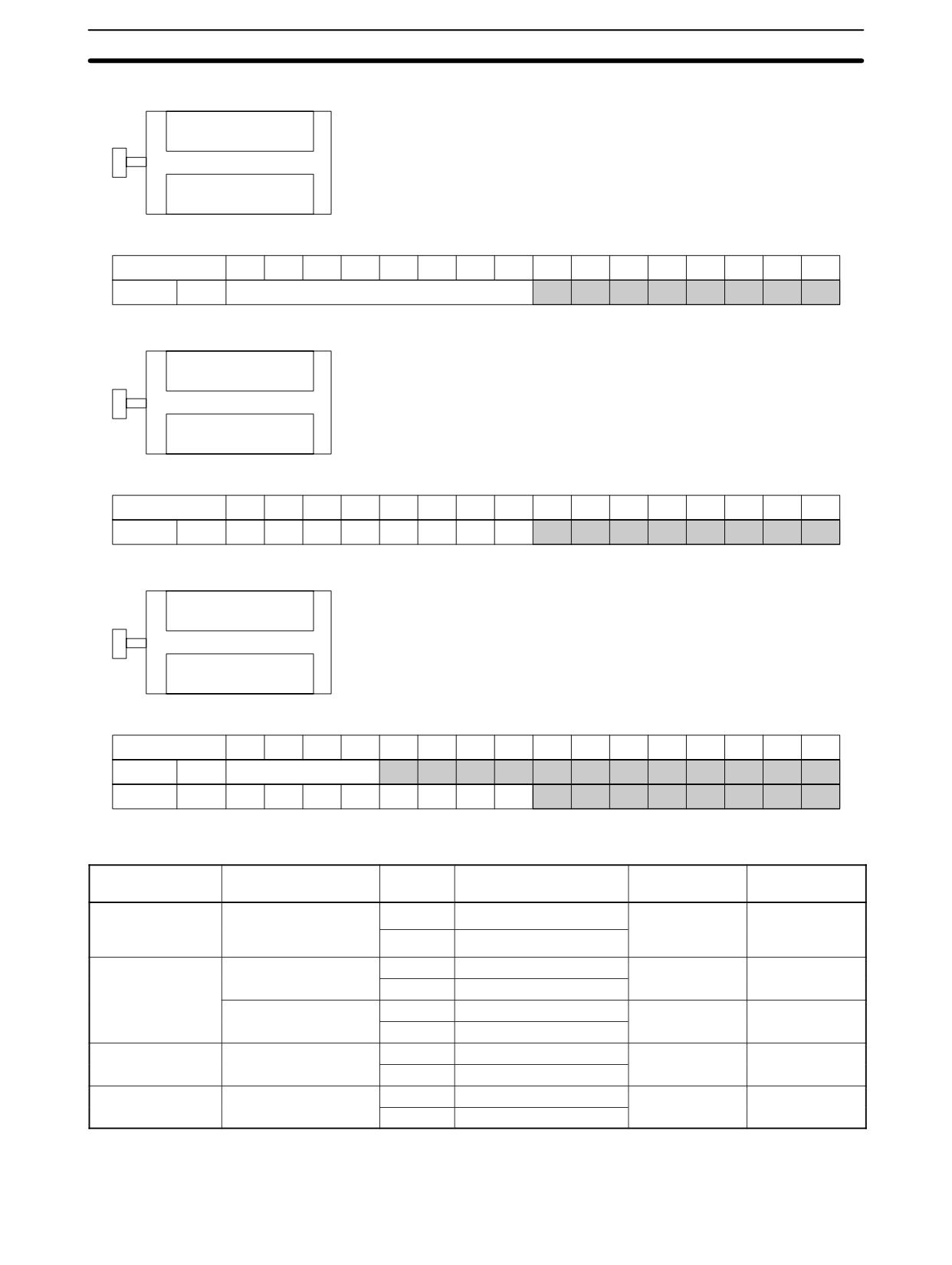
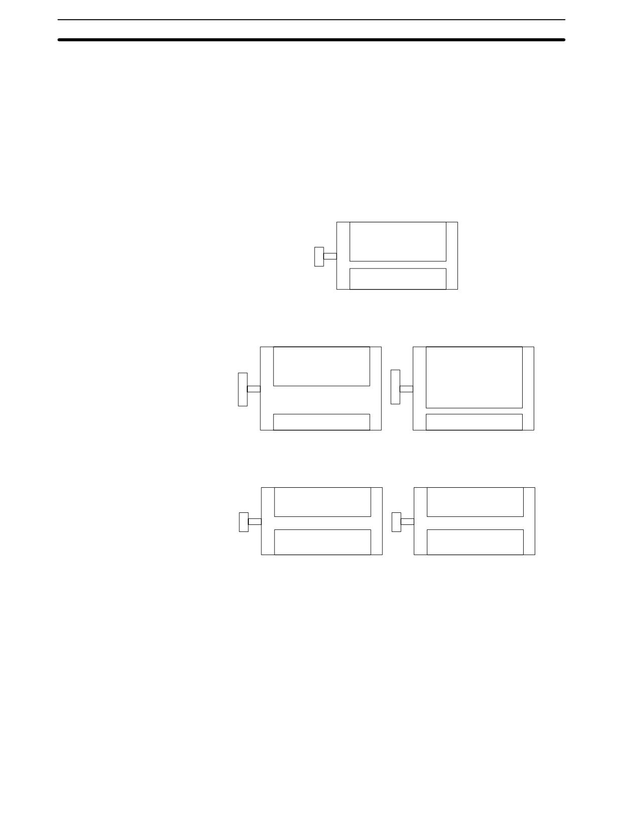
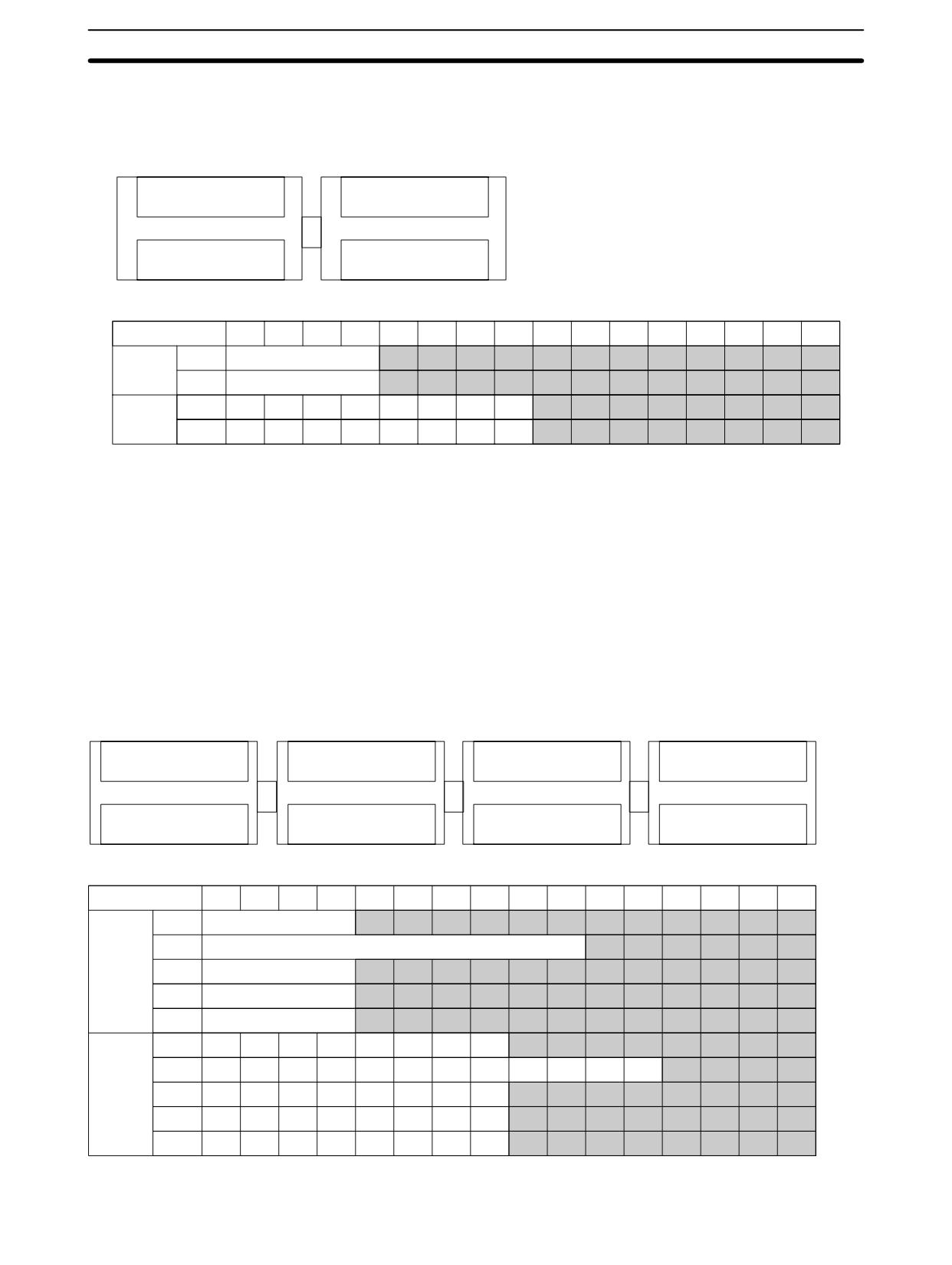
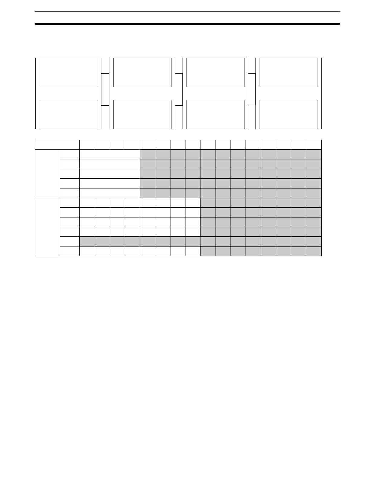
Host Link Commands
Section
4-5
Parameters
Name, Word address (Command)
In “Name,” specify the area (i.e., IR, SR, LR, HR, AR, or TC) that is to be forced
set or reset. Specify the name in four characters. In “Word address,” specify the
address of the word that is to be forced set or reset.
Name
Classification
Word address setting range
OP1
OP2
OP3
OP4
CPM2A/CPM2C
CPM1/CPM1A/
PCs
SRM1(-V2) PCs
C
I
O
(Space)
IR or SR
0000 to 0049
0000 to 0019
0200 to 0252
0200 to 0252
L
R
(Space)
(Space)
LR
0000 to 0015
0000 to 0015
H
R
(Space)
(Space)
HR
0000 to 0019
0000 to 0019
A
R
(Space)
(Space)
AR
0000 to 0023
0000 to 0015
T
I
M
(Space)
Completion Flag (timer)
0000 to 0255
0000 to 0127
T
I
M
H
Completion Flag (high-speed timer)
0000 to 0255
0000 to 0127
T
I
M
L
Completion Flag (long timer)
0000 to 0255
0000 to 0127
T
M
H
H
Completion Flag (very high-speed timer)
0000 to 0255
0000 to 0127
C
N
T
(Space)
Completion Flag (counter)
C
N
T
R
Completion Flag (reversible counter)
Forced set/Reset/Cancel data (Command)
If a timer or counter completion flag is specified, only bit 15 is effective and all
other bits will be ignored. Only force-setting and force-resetting are possible for
timers/counters.
If a word address is specified, the content of the word specifies the desired pro-
cess for each bit in the specified word, as shown in the following table.
Hexadecimal setting
Process
0000
No action (bit status not changed)
0002
Reset
0003
Set
0004
Forced-reset
0005
Forced-set
0008
Forced set/reset status cancel
The bits that are merely set or reset may change status the next time the pro-
gram is executed, but bits that are force-set or force-reset will maintain the
forced status until it is cleared.
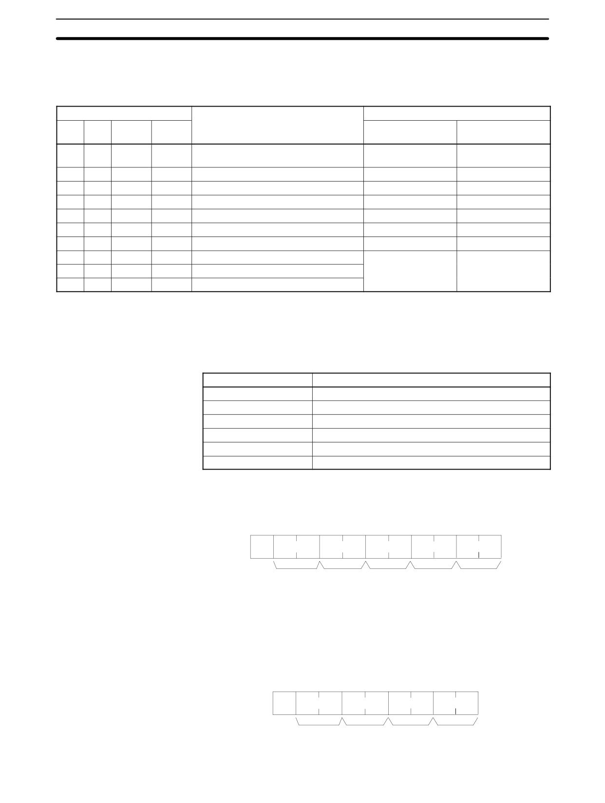
Response Format
An end code of 00 indicates normal completion.
@
x 101
x 10
0
F
K
x 161 x 160
:
↵
Node no.
Header
End code
FCS
Terminator
code
4-5-25 FORCED SET/RESET CANCEL - KC
Cancels all forced set and forced reset bits (including those set by FORCED
SET, FORCED RESET, and MULTIPLE FORCED SET/RESET). If multiple bits
are set, the forced status will be cancelled for all of them. It is not possible to can-
cel bits one by one using KC.
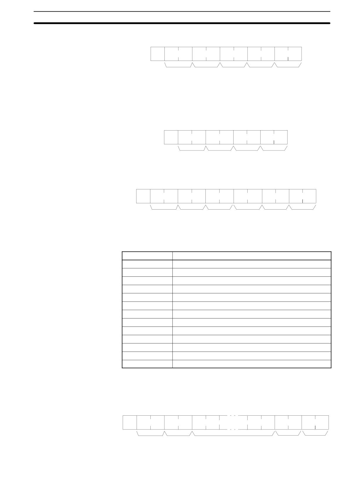
Command Format
@
x 101
x 10
0
K
C
:
↵
Node no.
Header
FCS
Terminator
code
295
Host Link Commands
Section
4-5
Response Format
An end code of 00 indicates normal completion.
@
x 101
x 10
0
K
C
x 161 x 160
:
↵
Node no.
Header
End code
FCS
Terminator
code
4-5-26 PC MODEL READ - MM
Reads the model type of the PC.
Command Format
0
@
x 101
x 10
M
M
:
↵
Node no.
Header
FCS
Terminator
code
Response Format
An end code of 00 indicates normal completion.
@
x 101
x 10
0
M
M
x 161 x 160
x 16
1 x 160
:
↵
Node no.
Header
End code
Model
FCS
Terminator
code
code
Parameters
Model Code
“Model code” indicates the PC model in two digits hexadecimal.
Model code
Model
01
C250
02
C500
03
C120
0E
C2000
10
C1000H
11
C2000H/CQM1/CPM2A/CPM2C/CPM1/CPM1A/SRM1(-V2)
12
C20H/C28H/C40H/C200H/C200HS
20
CV500
21
CV1000
22
CV2000
40
CVM1-CPU01-E
41
CVM1-CPU11-E
42
CVM1-CPU21-E
4-5-27 TEST - TS
Returns, unaltered, one block of data transmitted from the host computer.
Command Format
@
x 101
x 10
0
T
S
122 characters max.
:
↵
Node no.
Header
Characters
FCS
Terminator
code
296
Host Link Commands
Section
4-5
Response Format
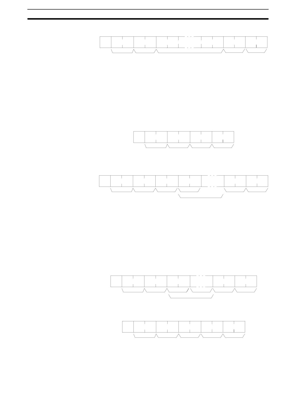
An end code of 00 indicates normal completion.
0
@
x 101
x 10
T
S
122 characters max.
:
↵
Node no.
Header
Characters
FCS
Terminator
code
Parameters
Characters (Command, Response)
For the command, this setting specifies any characters other than the carriage
return (CHR$(13)). For the response, the same characters as specified by the
command will be returned unaltered if the test is successful.
4-5-28 PROGRAM READ - RP
Reads the contents of the PC user’s program area in machine language (object
code). The contents are read as a block, from the beginning to the end.
Command Format
@
x 101
x 10
0
R
P
:
↵
Node no.
Header
FCS
Terminator
code
Response Format
An end code of 00 indicates normal completion.
0
@
x 101
x 10
R
P
x 161 x 160
x 16
1 x 160
:
↵
Node no.
Header
End code
1 byte
FCS
Terminator
code
Program (for entire UM area)
Parameters
Program (Response)
The program is read from the entire program area.
Note To stop this operation in progress, execute the ABORT (XZ) command.
4-5-29 PROGRAM WRITE - WP
Writes to the PC user’s program area the machine language (object code) pro-
gram transmitted from the host computer. The contents are written as a block,
from the beginning.
Command Format
0
@
x 101
x 10
W
P
x 161 x 160
:
↵
Node no.
Header
1 byte
FCS
Terminator
code
Program (Up to maximum memory size)
Response Format
An end code of 00 indicates normal completion.
@
x 101
x 10
0
W
P
x 161 x 160
:
↵
Node no.
Header
End code
FCS
Terminator
code
Parameters
Program (Command)
Program data up to the maximum memory size.
297
Host Link Commands
Section
4-5
4-5-30 COMPOUND COMMAND - QQ
Registers at the PC all of the bits, words, and timers/counters that are to be read,
and reads the status of all of them as a batch.
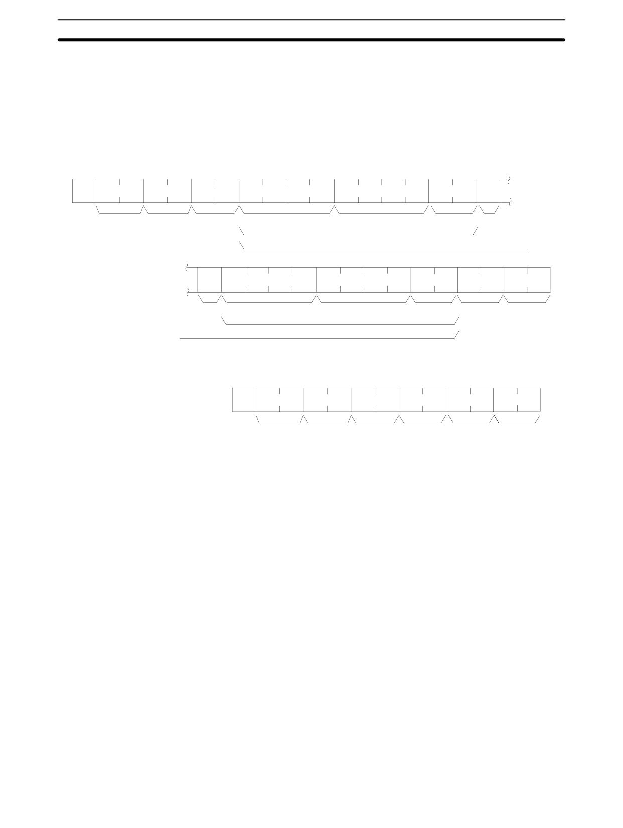
Registering Read Information
Register the information on all of the bits, words, and timers/counters that are to
be read.
Command Format
0
@
x 101
x 10
Q
Q
M
R
OP1 OP2 OP3 OP4
x 103 x 102 x 101 x 100
OP1 OP2
,
Node no.
Header
Sub-header
Read area
Read word address
Data
Data break
code
code
format
Single read information
Total read information (128 max.)
OP1 OP2 OP3 OP4
x 103 x 102 x 101 x 100
OP1 OP2
:
↵
,
Data break
Read area
Read word address
Data
FCS
Terminator
format
Single read information
Total read information (128 max.)
Response Format
An end code of 00 indicates normal completion.
@
x 101
x 10
0
Q
Q
M
R
x 161 x 160
:
↵
Node no.
Header
Sub-header End code
FCS
Terminator
code
code
Parameters
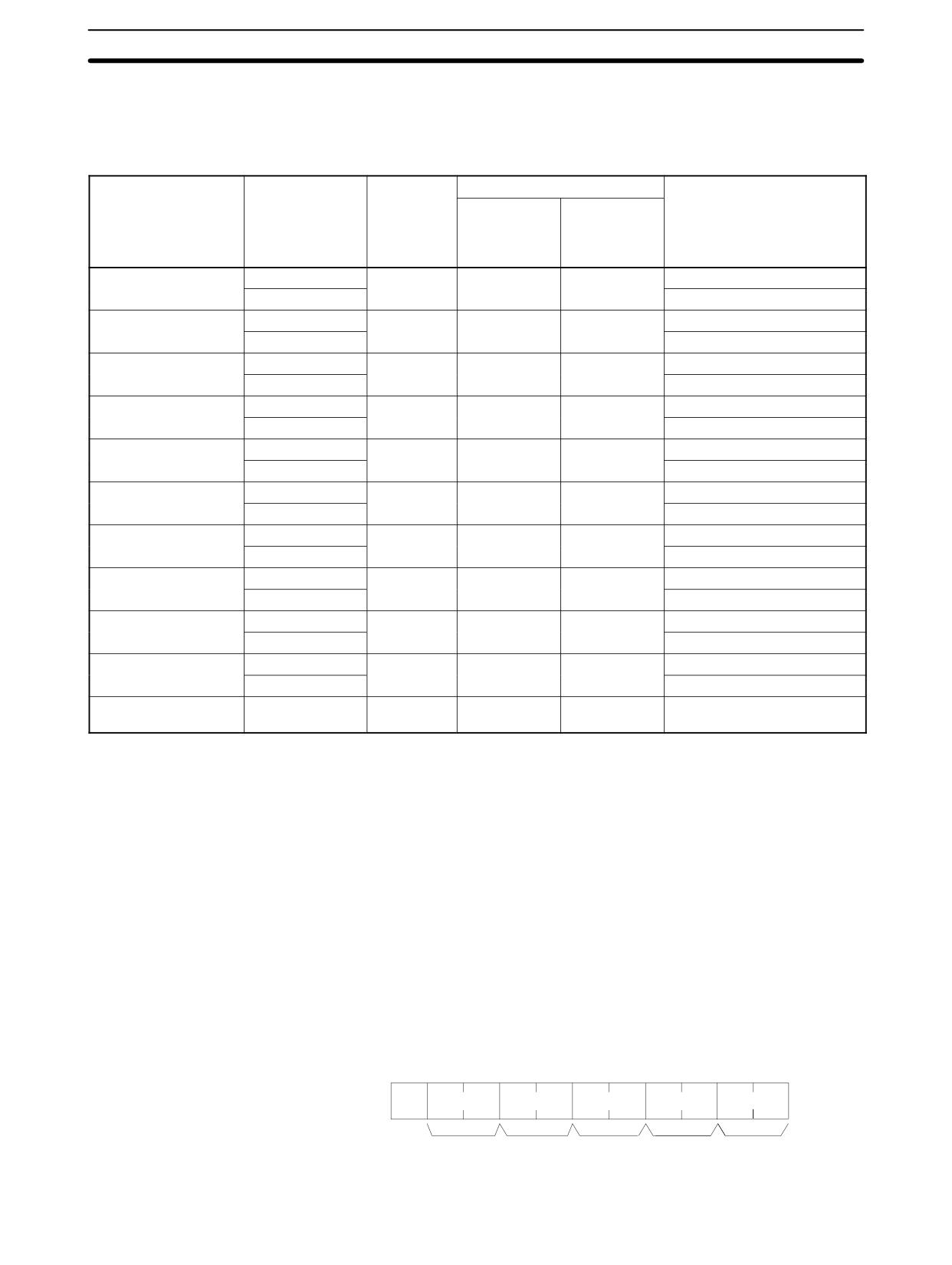
Read Area (Command)
Specify in four-character code the area that is to be read. The codes that can be
specified are listed in the following table.
298
Host Link Commands
Section
4-5
Read Word address, Data Format (Command)
Depending on the area and type of data that are to be read, the information to be
read is as shown in the following table. The “read data” is specified in four digits
BCD, and the data format is specified in two digits BCD.
Area
Read data
Read area
Read word
Data format
cl
assificat
ion
CPM2A/
CPM1/
CPM2C PCs
CPM1A/
SRM1(-V2)
PCs
IR or SR
Bit
C I O (S)
0000 to 0049
0000 to 0019
00 to 15 (decimal)
0200 to 0255
0200 to 0255
Word
“CH”
LR
Bit
L R (S) (S)
0000 to 0015
0000 to 0015
00 to 15 (decimal)
Word
“CH”
HR
Bit
H R (S) (S)
0000 to 0019
0000 to 0019
00 to 15 (decimal)
Word
“CH”
AR
Bit
A R (S) (S)
0000 to 0023
0000 to 0015
00 to 15 (decimal)
Bit
“CH”
Timer
Completion Flag
T I M (S)
0000 to 0255
0000 to 0127
2 characters other than “CH”
PV
“CH”
High-speed timer
Completion Flag
T I M H
0000 to 0255
0000 to 0127
2 characters other than “CH”
PV
“CH”
Long timer
Completion Flag
T I M L
0000 to 0255
Not used.
2 characters other than “CH”
PV
“CH”
Very high-speed timer
Completion Flag
T M H H
0000 to 0255
Not used.
2 characters other than “CH”
PV
“CH”
Counter
Completion Flag
C N T (S)
0000 to 0255
0000 to 0127
2 characters other than “CH”
PV
“CH”
Reversible counter
Completion Flag
C N T R
0000 to 0255
0000 to 0127
2 characters other than “CH”
PV
“CH”
DM
Word
D M (S) (S)
0000 to 2047
0000 to 1023*
Any 2 characters
6144 to 6655
6144 to 6655
Note *For SRM1(-V2) PCs, the DM range is from 0000 to 2047.
(S): Space
Data Break (Command)
The read information is specified one item at a time separated by a break code
(,). The maximum number of items that can be specified is 128. (When the PV of
a timer/counter is specified, however, the status of the Completion Flag is also
returned, and must therefore be counted as two items.)
Batch Reading
The bit, word, and timer/counter status is read as a batch according to the read
information that was registered with QQ.
Command Format
@
x 101
x 10
0
Q
Q
I
R
:
↵
Node no.
Header
Sub-header
FCS
Terminator
code
code
299

Host Link Commands
Section
4-5
Response Format
An end code of 00 indicates normal completion.
0
ON/
@
x 101
x 10
Q
Q
I
R
x 161 x 160
x 103 x 102 x 101 x 100
,
OFF
Node no.
Header
Sub-header End code
Timer/counter
Data break
code
code
If PV is specified the status
of the Completion Flag is
also returned.
ON/
,
,
,
x 163 x 162 x 161 x 160
:
↵
OFF
Word data
FCS
Terminator
Bit data
IR, SR, LR, HR,
ON/OFF
AR, DM
Parameters
Read Data (Response)
Read data is returned according to the data format and the order in which read
information was registered using QQ. If “Completion Flag” has been specified,
then bit data (ON or OFF) is returned. If “Word” has been specified, then word
data is returned. If “PV” has been specified for timers/counters, however, then
the PV is returned following the Completion Flag.
Data Break (Response)
The break code (, ) is returned between sections that are read.
4-5-31 ABORT - XZ
Aborts the Host Link operation that is currently being processed, and then en-
ables reception of the next command. The ABORT command does not receive a
response.
Command Format
@
x 101
x 10
0
X
Z
:
↵
Node no.
Header
FCS
Terminator
code
4-5-32 INITIALIZE - ::
Initializes the transmission control procedure of all the PCs connected to the
host computer. The INITIALIZE command does not use node numbers or FCS,
and does not receive a response.
Command Format
@
:
:
↵
4-5-33 TXD RESPONSE - EX
This command is supported by CPM2A/CPM2C PCs only.
This is the response format used when the PC’s TXD(48) instruction is executed
in Host Link communications mode. There is no command associated with EX.
TXD(48) converts the specified data into ASCII and transmits it to the host com-
puter with this format. The response can contain up to 122 characters of ASCII
data. (TXD(48) does not support multiple frames.)
300

Host Link Commands
Section
4-5
Response Format
An end code of 00 indicates normal completion.
@
x 101
x 10
0
T
S
Data specified in TXD(48)
:
↵
Node no.
Header
Characters
FCS
Terminator
code
(122 max.)
Parameters
Characters (Response)
This is the data specified in TXD(48) that has been converted to ASCII.
4-5-34 Undefined Command - IC
This response is returned if the header code of a command cannot be decoded.
Check the header code.
Response Format
0
@
x 101
x 10
I
C
:
↵
Node no.
Header
FCS
Terminator
code
301
SECTION 5
Memory Areas
This section describes the structure of the PC memory areas and explains how to use them.
5-1
Memory Area Functions
304
5-1-1
Memory Area Structure
304
5-1-2
Functions
307
5-1-3
CPM1/CPM1A/SRM1(-V2) Flash Memory
309
5-2
I/O Allocation for CPM1/CPM1A/CPM2A PCs
309
5-2-1
CPU Units
309
5-2-2
Expansion I/O Units
313
5-2-3
Expansion Units
314
5-2-4
Examples of Expansion Unit and Expansion I/O Unit Allocation
315
5-3
I/O Allocation for CPM2C PCs
319
5-3-1
CPU Units
319
5-3-2
Expansion I/O Units
321
5-3-3
Expansion Units
324
5-3-4
Examples of Expansion Unit and Expansion I/O Unit Allocation
325
303

Memory Area Functions
Section
5-1
5-1
Memory Area Functions
5-1-1
Memory Area Structure
CPM1/CPM1A
The following memory areas can be used with the CPM1/CPM1A.
Data area
Words
Bits
Function
IR area1
Input area
IR 000 to IR 009
IR 00000 to IR 00915
These bits are allocated to the external I/O
(10 words)
(160 bits)
terminals.
Output area
IR 010 to IR 019
IR 01000 to IR 01915
(10 words)
(160 bits)
Work area
IR 200 to IR 231
IR 20000 to IR 23115
Work bits can be freely used within the pro-
(32 words)
(512 bits)
gram.
SR area
SR 232 to SR 255
SR 23200 to SR 25515
These bits serve specific functions such as
(24 words)
(384 bits)
flags and control bits.
TR area
---
TR 0 to TR 7
These bits are used to temporarily store
(8 bits)
ON/OFF status at program branches.
HR area2
HR 00 to HR 19
HR 0000 to HR 1915
These bits store data and retain their ON/
(20 words)
(320 bits)
OFF status when power is turned off, or op-
eration starts or stops. They are used in the
same way as work bits.
AR area2
AR 00 to AR 15
AR 0000 to AR 1515
These bits serve specific functions such as
(16 words)
(256 bits)
flags and control bits.
LR area1
LR 00 to LR 15
LR 0000 to LR 1515
Used for a 1:1 PC Link with another PC.
(16 words)
(256 bits)
Timer/Counter area2
TC 000 to TC 127 (timer/counter numbers)3
Timers and counters use the TIM,
TIMH(15), CNT and CNTR(12) instructions.
The same numbers are used for both timers
and counters.
DM area
Read/write2
DM 0000 to DM 0999
---
DM area data can be accessed in word
DM 1022 to DM 1023
units only. Word values are retained when
(1,002 words)
the power is turned off, or operation started
or stopped.
Read/write areas can be read and written
freely within the program.
Error log
DM 1000 to DM 1021
---
Used to store the time of occurrence and
(22 words)
error code of errors that occur. These words
can be used as ordinary read/write DM
when the error log function is not being
used.
Read-only4
DM 6144 to DM 6599
---
Cannot be overwritten from program.
(456 words)
PC Setup4
DM 6600 to DM 6655
---
Used to store various parameters that con-
(56 words)
trol PC operation.
Note
1. IR and LR bits that are not used for their allocated functions can be used as
work bits.
2. The contents of the HR area, AR area, Counter area, and read/write DM
area are backed up by a capacitor. The backup time varies with the ambient
temperature, but at 25_C, the capacitor will back up memory for 20 days. If
the power supply is off longer than the backup time, memory contents will be
cleared and AR1314 will turn ON. (This flag turns ON when data can no
longer be retained by the built-in capacitor.) Refer to 2-1-2 Characteristics in
the CPM1 and CPM1A Operation Manual for a graph showing the backup
time vs. temperature.
3. When accessing a PV, TC numbers are used as word data; when accessing
Completion Flags, they are used as bit data.
4. Data in DM 6144 to DM 6655 cannot be overwritten from the program, but
they can be changed from a Programming Device.
304

Memory Area Functions
Section
5-1
CPM2A/CPM2C
The following memory areas can be used with the CPM2A/CPM2C.
Data area
Words
Bits
Function
IR area1
Input area
IR 000 to IR 009
IR 00000 to IR 00915
These bits are allocated to the external I/O
(10 words)
(160 bits)
terminals.
Output area
IR 010 to IR 019
IR 01000 to IR 01915
(10 words)
(160 bits)
Work area
IR 020 to IR 049,
IR 02000 to IR 04915,
Work bits can be freely used within the pro-
IR 200 to IR 227
IR 20000 to IR 22715
gram.
(58 words)
(928 bits)
SR area
SR 228 to SR 255
SR 22800 to SR 25515
These bits serve specific functions such as
(28 words)
(448 bits)
flags and control bits.
TR area
---
TR 0 to TR 7
These bits are used to temporarily store
(8 bits)
ON/OFF status at program branches.
HR area2
HR 00 to HR 19
HR 0000 to HR 1915
These bits store data and retain their ON/
(20 words)
(320 bits)
OFF status when power is turned OFF, or
operation starts or stops. They are used in
the same way as work bits.
AR area2
AR 00 to AR 23
AR 0000 to AR 2315
These bits serve specific functions such as
(24 words)
(384 bits)
flags and control bits.
LR area1
LR 00 to LR 15
LR 0000 to LR 1515
Used for a 1:1 PC Link with another PC.
(16 words)
(256 bits)
Timer/Counter area2
TC 000 to TC 255 (timer/counter numbers)3
Timers and counters use the TIM,
TIMH(15), CNT, CNTR(12), TMHH(--), and
TIML(--) instructions. The same numbers
are used for both timers and counters.
DM area
Read/write2
DM 0000 to DM 1999
---
DM area data can be accessed in word
DM 2022 to DM 2047
units only. Word values are retained when
(2,026 words)
the power is turned off, or operation started
or stopped.
Read/write areas can be read and written
freely within the program.
Error log
DM 2000 to DM 2021
---
Used to store the time of occurrence and
(22 words)
error code of errors that occur. These words
can be used as ordinary read/write DM
when the error log function isn’t being used.
Read-only4,5
DM 6144 to DM 6599
---
Cannot be overwritten from program.
(456 words)
PC Setup4,5
DM 6600 to DM 6655
---
Used to store various parameters that con-
(56 words)
trol PC operation.
Note
1. IR and LR bits that are not used for their allocated functions can be used as
work bits.
2. The contents of the HR area, AR area, Counter area, and read/write DM
area are backed up by the CPU Unit’s battery. If the battery is removed or
fails, the contents of these areas will be lost and returned to default values.
(In CPM2C CPU Units without a battery, these areas are backed up by a ca-
pacitor.)
3. When a TC numbers is used as a word operand, the timer or counter PV is
accessed; when used as a bit operand, its Completion Flag is accessed.
4. Data in DM 6144 to DM 6655 cannot be overwritten from the program, but
they can be changed from a Programming Device.
5. The program and data in DM 6144 to DM 6655 are stored in flash memory.
305

Memory Area Functions
Section
5-1
SRM1(-V2)
The following memory areas can be used with the SRM1(-V2).
Data area
Words
Bits
Function
IR area1
Input area
IR 000 to IR 007
IR 00000 to IR 00715
These bits are allocated to the external I/O
(8 words)
(128 bits)
terminals. The ON/OFF status of the I/O
bits will be the same as the ON/OFF status
of the I/O terminals
Output area
IR 010 to IR 017
IR 01000 to IR 01715
(When the CompoBus/S is used in 128-bit
(8 words)
(128 bits)
mode, IR 004 to IR 007 and IR 014 to
IR 017 can also be used as work bits.)
Work area
IR 008 to IR 009
IR 00800 to IR 00915
Work bits can be freely used within the pro-
IR 018 to IR 019
IR 01800 to IR 01915
gram. IR 232 to IR 239 however, are used
IR 200 to IR 239
IR 20000 to IR 23915
as the MACRO input area when MCRO(99)
(44 words)
(704 bits)
is being used.
SR area
SR 240 to SR 255
SR 24000 to SR 25507
These bits serve specific functions such as
(16 words)
(248 bits)
flags and control bits.
TR area
---
TR 0 to TR 7
These bits are used to temporarily store
(8 bits)
ON/OFF status at program branches.
HR area2
HR 00 to HR 19
HR 0000 to HR 1915
These bits store data and retain their ON/
(20 words)
(320 bits)
OFF status when power is turned off, or op-
eration starts or stops. They are used in the
same way as work bits.
AR area2
AR 00 to AR 15
AR 0000 to AR 1515
These bits serve specific functions such as
(16 words)
(256 bits)
flags and control bits. AR 04 to 07 are used
as slaves. Refer to AR Area.
LR area1
LR 00 to LR 15
LR 0000 to LR 1515
Used for a 1:1 PC Link with another PC.
(16 words)
(256 bits)
Timer/Counter area2
TC 000 to TC 127 (timer/counter numbers)3
Timers and counters use the TIM,
TIMH(15), CNT and CNTR(12) instructions.
The same numbers are used for both timers
and counters.
DM area
Read/write2
DM 0000 to DM 1999
---
DM area data can be accessed in word
(2,000 words)
units only. Word values are retained when
the power is turned off, or operation started
or stopped.
Read/write areas can be read and written
freely within the program.
Error log
DM 2000 to DM 2021
---
Used to store the time of occurrence and
(22 words)
error code of errors that occur. These words
can be used as ordinary read/write DM
when the error log function is not being
used.
Read-only4
DM 6144 to DM 6599
---
Cannot be overwritten from program.
(456 words)
PC Setup4
DM 6600 to DM 6655
---
Used to store various parameters that con-
(56 words)
trol PC operation.
Note
1. IR and LR bits that are not used for their allocated functions can be used as
work bits.
2. The contents of the HR area, AR area, Counter area, and read/write DM
area are backed up by a capacitor or a battery. Refer to 2-1-2 Characteristics
in the SRM1 Master Control Unit Operation Manual for a graph showing the
backup time vs. temperature.
3. When accessing a PV, TC numbers are used as word data; when accessing
Completion Flags, they are used as bit data.
4. Data in DM 6144 to DM 6655 cannot be overwritten from the program, but
they can be changed from a Programming Device.
306
Memory Area Functions
Section
5-1
5-1-2
Functions
IR Area
The functions of the IR area are explained below.
With CPM1, CPM1A, CPM2A, and CPM2C PCs, IR area bits from IR 00000 to
IR 01915 are allocated to terminals on the CPU Unit and Expansion I/O Units.
With the SRM1(-V2), IR area bits from IR 00000 to IR 00715 and IR 01000 to IR
01715 are allocated to CompoBus/S Slaves. They reflect the ON/OFF status of
input and output signals. Input bits begin at IR 00000, and output bits begin at
IR 01000.
IR words that are not allocated to inputs or outputs can be used as work words. In
addition, unused bits in IR words allocated to outputs can be used as work bits.
Work Bits
The work bits can be used freely within the program. They can only be used with-
in the program, however, and not for direct external I/O.
Note
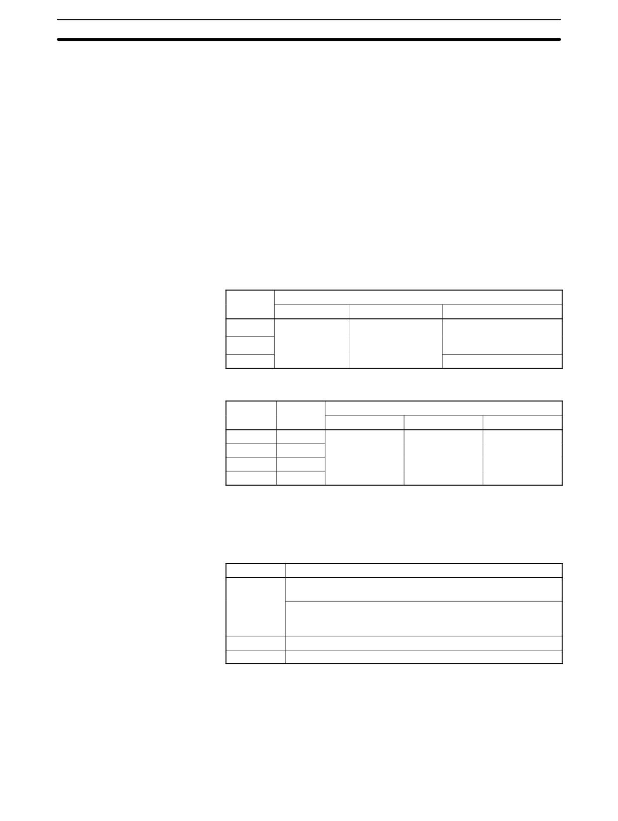
1. The input bits shown in the following tables can operate as normal inputs or
they can be assigned special functions in the PC Setup.
Special functions for input bits IR 00000 through IR 00002 are set in
DM 6642:
Bit
PC Setup setting (DM 6642 bits 08 to15)
address
00
01
02, 03, or 04
IR 00000
Used as normal
Used as high-speed
Used as inputs for
inputs
counter inputs
synchronized pulse
IR 00001
control.
IR 00002
Used as a normal input.
Special functions for input bits IR 00003 through IR 00006 are set in
DM 6628:
Bit
Bits in
PC Setup setting (in DM 6628)
address
DM 6628
0
1
2
IR 00003
00 to 03
Used as normal
Used as
Used as
inputs.
interrupt
inputs
quick-response
IR 00004
04 to 07
(including
inputs
IR 00005*
08 to 11
counter mode).
IR 00006*
12 to 15
Note *Input 00006 does not exist and input 00005 must be used as a nor-
mal input in CPM2C CPU Units with 10 I/O points.
2. Output bits IR 01000 and IR 01001 can operate as normal inputs or they can
be used for pulse outputs with PULS(65), SYNC(--), or PWM(--). (Use a
CPU Unit with transistor outputs for the pulse output functions.)
Instruction
Function
PULS(65)
With SPED(64):
Single-phase pulse output without acceleration or deceleration
With ACC(--):
Single-phase pulse output with trapezoidal acceleration and
deceleration
SYNC(--)
Synchronized pulse control output
PWM(--)
Variable duty-ratio pulse output
SR Area
These bits mainly serve as flags to PC operation or contain present and set val-
ues for various functions. For details on the various bit functions, refer to relevant
sections in this manual or to Appendix C Memory Areas.
Some SR area words can be used as work words when they are not used for
their assigned purpose.
TR Area
When a complex ladder diagram cannot be programmed in mnemonic code just
as it is, these bits are used to temporarily store ON/OFF execution conditions at
307
Memory Area Functions
Section
5-1
program branches. They are used only for mnemonic code. When programming
directly with ladder diagrams using the SYSMAC Support Software (SSS) or the
SYSMAC-CPT Support Software, TR bits are automatically processed for you.
The same TR bits cannot be used more than once within the same instruction
block, but can be used again in different instruction blocks. The ON/OFF status
of TR bits cannot be monitored from a Programming Device.
Examples showing the use of TR bits in programming are provided on page 346.
HR Area
These bits retain their ON/OFF status even after the PC power supply has been
turned off or when operation begins or stops. They are used in the same way as
work bits.
AR Area
These bits mainly serve as flags related to PC operation. These bits retain their
status even after the PC power supply has been turned off or when operation
begins or stops. For details on the various bit functions, refer to relevant sections
in this manual or to Appendix C Memory Areas.
LR Area
When the CPM1/CPM1A/CPM2A/CPM2C/SRM1(-V2) is linked 1:1 with anoth-
er CPM1/CPM1A/CPM2A/CPM2C/SRM1(-V2), a CQM1, an C200HS or
C200HX/HG/HE PC, these bits are used to share data. For details, refer to page
225.
LR bits can be used as work bits when not used for 1:1 PC Links.
Timer/Counter Area
This area is used to manage timers and counters created with TIM, TIMH(15),
TMHH(--)*, TIML(--)*, CNT, and CNTR(12). The same numbers are used for
both timers and counters and each number can be used only once in the user
program. Do not use the same TC number twice even for different instructions.
Use TC numbers 000 through 003 for TIMH(15) and TC numbers 004 to 007 for
TMHH(--)*. When these timer numbers are used, timing is performed as an in-
terrupt process and the cycle timer does not affect timer operation.
TC numbers are used to create timers and counters, as well as to access
Completion Flags and present values (PVs). If a TC number is designated for
word data, it will access the present value (PV); if it is used for bit data, it will ac-
cess the Completion Flag for the timer/counter.
Refer to instructions beginning on page 384 for details on timers and counters.
DM Area
DM area data is accessed in word units only. The contents of the DM area are
retained even after the PC power supply has been turned off or when operation
begins or stops.
CPM1/CPM1A
DM words DM 0000 through DM 0999, DM 1022, and DM 1023 can be used
freely in the program; other DM words are allocated specific functions, de-
scribed below.
DM 1000 through DM 1021 contain the error log information. Refer to Section 9
Troubleshooting for details on the error log.
CPM2A/CPM2C
DM words DM 0000 through DM 1999 and DM 2022 through DM 2047 can be
used freely in the program; other DM words are allocated specific functions, de-
scribed below.
DM 2000 through DM 2021 contain the error log information. Refer to Section 9
Troubleshooting for details on the error log.
SRM1(-V2)
DM words DM 0000 through DM 1999 can be used freely in the program; other
DM words are allocated specific functions, described below.
DM 2000 through DM 2021 contain the error log information. Refer to Section 9
Troubleshooting for details on the error log.
Note DM 6600 through DM 6655 contain the PC Setup. Refer to 1-1 PC Setup for de-
tails.
308

I/O Allocation for CPM1/CPM1A/CPM2A PCs
Section
5-2
5-1-3
CPM1/CPM1A/SRM1(-V2) Flash Memory
The following settings must be made to use the flash memory area for
CPM1/CPM1A/SRM1(-V2) PCs.
Writing Data
In order to write the contents of the UM area, the DM read-only area (DM 6144 to
DM 6599, and the PC Setup area (DM 6600 to DM 6655) to the flash memory,
either one of the following operations must be performed.
• Switch the PC to either the MONITOR or PROGRAM mode.
• Turn the power to the PC OFF and ON again.
Note SRM1-CO01/02 Capacitor Backup
If changes are made to the above memory areas, they are not written to the flash
memory, and the power is switched off for 20 days or more (at 25°C), the
changes (in RAM) will be lost. If this occurs, the unchanged contents will be read
from the flash memory when the PC is started again.
Changing Memory Areas
When operating the SRM1 for the first time after changes have been made to the
UM area, the DM read only area (DM 6144 to DM 6599, and the PC Setup area
(DM 6600 to DM 6655), beware of the effect resulting from the SRM1’s delay in
the operation on other devices.
The first operation for the SRM1 after the above memory areas have been
changed will be a maximum of 850 ms later than the normal first operation with-
out changes.
SRM1 Cycle Times
A cycle time overflow warning will not be issued when any of the following opera-
tions are performed in either MONITOR or OPERATION modes. Be careful of
the effect of using online editing on SRM1 I/O response time.
• Changes to the program using online editing.
• Changes to the read-only DM area (DM 6144 to DM 6599.)
• Changes to the PC Setup area (DM 6600 to DM 6655.)
When any of the above operations are performed, the SRM1 cycle time will be
increased by a maximum of 850 ms. During this tiny interrupts will be disabled
while the program or memory contents is written.
5-2
I/O Allocation for CPM1/CPM1A/CPM2A PCs
5-2-1
CPU Units
CPM1
No. of I/O
Model number
I/O
Allocated bits
Max. No. of
Max. No. of I/O
(on CPU Unit)
Expansion I/O
(see note 1)
Units
10
CPM1-10CDR-j
Input
6 inputs: 00000 to 00005
1 (see note 1)
30
Output
4 outputs: 01000 to 01003
20
CPM1-20CDR-j
Input
12 inputs: 00000 to 00011
1 (see note 1)
40
Output
8 outputs: 01000 to 01007
30
CPM1-30CDR-j
Input
18 inputs:
1 (see note 1)
50
00000 to 00011
00100 to 00105
Output
12 outputs:
01000 to 01007
01100 to 01103
30
CPM1-30CDR-j-V1
Input
18 inputs:
3 (see note 2)
90
00000 to 00011
00100 to 00105
Output
12 outputs:
01000 to 01007
01100 to 01103
309

I/O Allocation for CPM1/CPM1A/CPM2A PCs
Section
5-2
Note
1. The values for the maximum number of I/O in the above table include I/O on
Expansion I/O Units.
2. When using a CPM1 CPU Unit other than the CPM1-30CDR-j-V1, one of
the following 20-point Expansion I/O Units can be connected to the PC:
• CPM1-20EDR (relay outputs)
• CPM1A-20EDRT (sinking transistor outputs)
• CPM1A-20EDT1 (sourcing transistor outputs)
3. When using the CPM1-30CDR-j-V1, up to 3 CPM1/CPM1A Expansion I/O
Units or CPM1A-MAD01 Analog I/O Units can be connected to the PC.
CPM1A
No. of I/O
Model number
I/O
Allocated bits
Max. No. of
Max. No. of I/O
(on CPU Unit)
Expansion I/O
(see note 1)
Units
10
CPM1A-10CDR-j
Input
6 inputs: 00000 to 00005
None
10
CPM1A-10CDT-D
CPM1A-10CDT1-D
Output
4 outputs: 01000 to 01003
20
CPM1A-20CDR-j
Input
12 inputs: 0000 to 00011
None
20
CPM1A-20CDT-D
Output
8 outputs: 01000 to 01007
CPM1A-20CDT1-D
30
CPM1A-30CDR-j
Inputs
18 inputs:
3 (see note)
90
CPM1A-30CDT-D
00000 to 00011
CPM1A-30CDT1-D
00100 to 00105
Output
12 outputs:
01000 to 01007
01100 to 01103
40
CPM1A-40CDR-j
Inputs
24 inputs:
3 (see note)
100
CPM1A-40CDT-D
00000 to 00011
CPM1A-40CDT1-D
00100 to 00111
Output
16 outputs:
01000 to 01007
01100 to 01107
Note
1. The values for the maximum number of I/O in the above table include I/O on
Expansion I/O Units.
2. When using a CPM1A CPU Unit with 30 or 40 I/O points, up to 3 Expansion
Units or Expansion I/O Units can be connected to the PC.
310

I/O Allocation for CPM1/CPM1A/CPM2A PCs
Section
5-2
CPM2A
No. of I/O
Model number
I/O
Allocated bits
Max. No. of
Max. No. of I/O
(on CPU Unit)
Expansion I/O
(see note 1)
Units
20
CPM2A-20CDR-j
Input
12 inputs: 0000 to 00011
3
80
CPM2A-20CDT-D
Output
8 outputs: 01000 to 01007
CPM2A-20CDT1-D
30
CPM2A-30CDR-j
Input
18 inputs:
3
90
CPM2A-30CDT-D
00000 to 00011
CPM2A-30CDT1-D
00100 to 00105
Output
12 outputs:
01000 to 01007
01100 to 01103
40
CPM2A-40CDR-j
Input
24 inputs:
3
100
CPM2A-40CDT-D
00000 to 00011
CPM2A-40CDT1-D
00100 to 00111
Output
16 outputs:
01000 to 01007
01100 to 01107
60
CPM2A-60CDR-j
Input
36 inputs:
3
120
CPM2A-60CDT-D
00000 to 00011
CPM2A-60CDT1-D
00100 to 00111
00200 to 00211
Output
24 outputs:
01000 to 01007
01100 to 01107
01200 to 01207
Note
1. The values for the maximum number of I/O in the above table include the I/O
on Expansion I/O Units.
2. When using a CPM2A CPU Unit, up to 3 Expansion Units or Expansion I/O
Units can be connected to the PC.
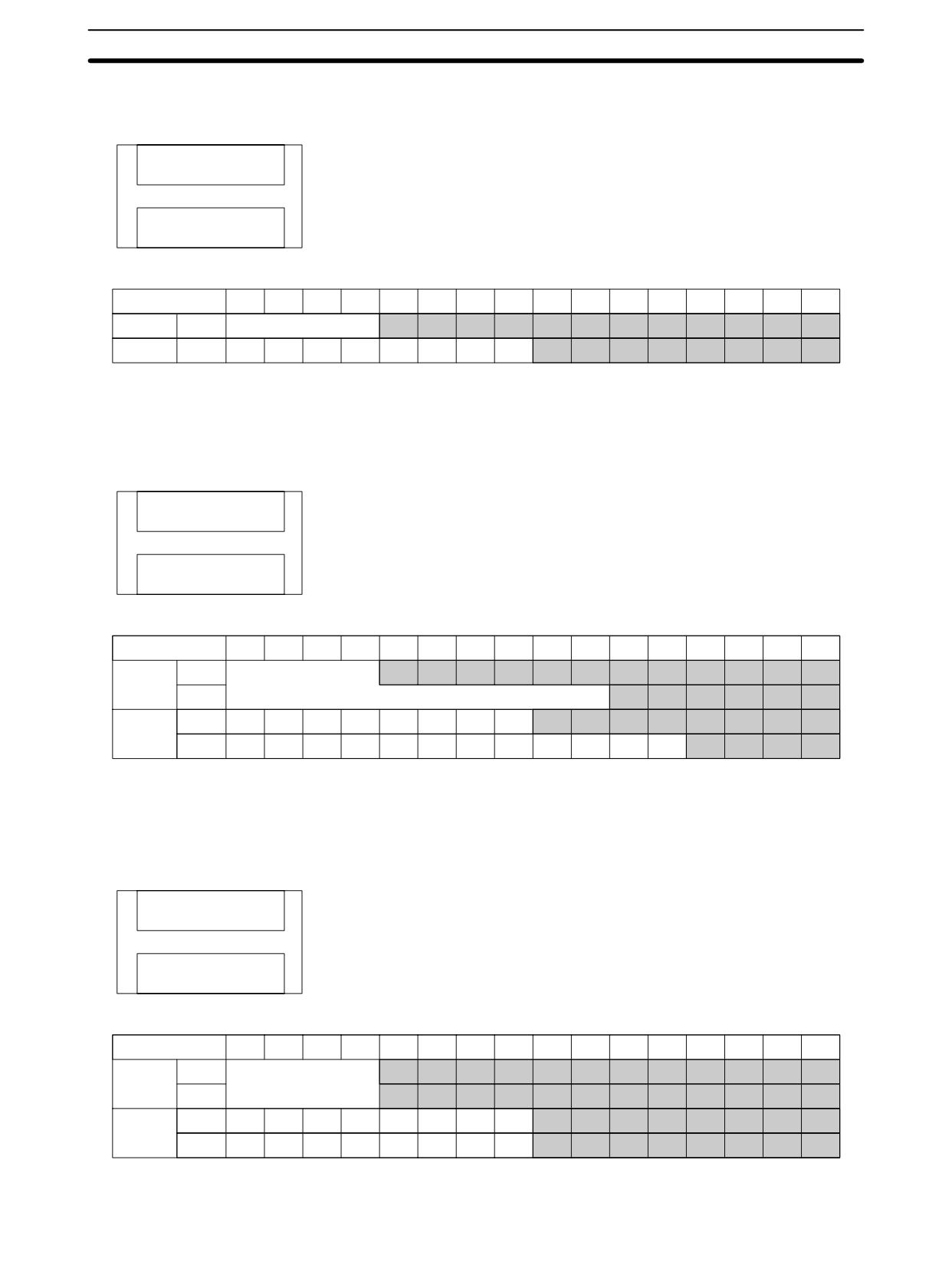
CPU Unit Allocation
• In the following diagrams, shaded areas indicate bits actually used for inputs or
outputs.
• Input bits are allocated starting from IR 00000.
• Output bits are allocated starting from IR 01000.
• Bits in the output words that are not used as output bits can be used as work
bits.
• Bits in the input words that are not used as input bits cannot be used as work
bits.
CPU Units with 10 I/O Points
6 inputs
CPM1-10CDR-j
IR 00000 to IR 00005
CPM1A-10CDj-j
4 outputs
IR 01000 to IR 01003
Bits
15
14
13
12
11
10
09
08
07
06
05
04
03
02
01
00
Inputs
IR 000
Do not use
Outputs
IR 010
311
I/O Allocation for CPM1/CPM1A/CPM2A PCs
Section
5-2
CPU Units with 20 I/O Points
12 inputs
CPM1-20CDR-j
IR 00000 to IR 00011
CPM1A-20CDj-j
CPM2A-20CDj-j
8 outputs
IR 01000 to IR 01007
Bits
15
14
13
12
11
10
09
08
07
06
05
04
03
02
01
00
Inputs
IR 000
Do not use
Outputs
IR 010
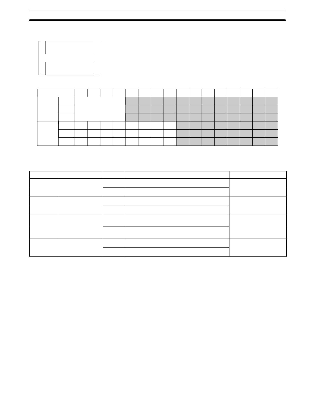
CPU Units with 30 I/O Points
18 inputs
IR 00000 to IR 00011
CPM1-30CDR-j/CPM1-30CDR-j-V1
IR 00100 to IR 00105
CPM1A-30CDj-j
CPM2A-30CDj-j
12 outputs
IR 01000 to IR 01007
IR 01100 to IR 01103
Bits
15
14
13
12
11
10
09
08
07
06
05
04
03
02
01
00
IR 000
Inputs
Do not use
IR 001
IR 010
Outputs
IR 011
CPU Units with 40 I/O Points
24 inputs
IR 00000 to IR 00011
CPM1A-40CDj-j
IR 00100 to IR 00111
CPM2A-40CDj-j
16 outputs
IR 01000 to IR 01007
IR 01100 to IR 01107
Bits
15
14
13
12
11
10
09
08
07
06
05
04
03
02
01
00
IR 000
Inputs
Do not use
IR 001
IR 010
Outputs
IR 011
312
I/O Allocation for CPM1/CPM1A/CPM2A PCs
Section
5-2
CPU Units with 60 I/O Points
36 inputs
IR 00000 to IR 00011
IR 00100 to IR 00111
CPM1A-60CDj-j
IR 00200 to IR 00211
24 outputs
IR 01000 to IR 01007
IR 01100 to IR 01107
IR 01200 to IR 01207
Bits
15
14
13
12
11
10
09
08
07
06
05
04
03
02
01
00
IR 000
Inputs
IR 001
Do not use
IR 002
IR 010
Outputs
IR 011
IR 012
5-2-2
Expansion I/O Units
No. of I/O
Model number
I/O
Allocated bits
Compatible CPU Units
8
CPM1A-8ED
Input
8 inputs: Word (m+1), bits 00 to 07
CPM1-30CDR-j-V1
CPM1A
Output
---
CPM2A
8
CPM1A-8ER
Input
---
CPM1-30CDR-j-V1
CPM1A-8ET
CPM1A
Output
8 outputs: Word (n+1), bits 00 to 07
CPM1A-8ET1
CPM2A
20
CPM1A-20EDR
Input
12 inputs: Word (m+1), bits 00 to 11
CPM1-30CDR-j-V1
CPM1A-20EDR1
CPM1A
CPM1A-20EDT
Output
8 outputs: Word (n+1), bits 00 to 07
CPM2A
CPM1A-20EDT1
20
CPM1A-20EDR
Input
12 inputs: Word (m+1), bits 00 to 11
CPM1-10CDR-j
CPM1-20CDR-j
Output
8 outputs: Word (n+1), bits 00 to 07
CPM1-30CDR-j(-V1)
Note m: “m” denotes the last input word allocated to the CPU Unit, or to the previous
Expansion Unit or Expansion I/O Unit if one is already connected.
n: “n” denotes the last output word allocated to the CPU Unit, or to the previous
Expansion Unit or Expansion I/O Unit if one is already connected.
Expansion I/O Unit Allocation
• In the following diagrams, shaded areas indicate bits actually used for inputs or
outputs.
• Input bits are allocated to Expansion I/O Units from word (m+1), where “m” is
the last input word allocated to the CPU Unit, or to the previous Expansion Unit
or Expansion I/O Unit if one is already connected.
• Output bits are allocated to Expansion I/O Units from word (n+1), where “n” is
the last output word allocated to the CPU Unit, or to the previous Expansion
Unit or Expansion I/O Unit if one is already connected.
• Bits in the output words that are not used as output bits can be used as work
bits.
• Bits in the input words that are not used as input bits cannot be used as work
bits.
313
I/O Allocation for CPM1/CPM1A/CPM2A PCs
Section
5-2
Expansion I/O Units with 8 Inputs
8 inputs
CPM1A-8ED
Word (m+1), bits 00 to 07
No outputs
Bits
15
14
13
12
11
10
09
08
07
06
05
04
03
02
01
00
Inputs
m+1
Do not use
Expansion I/O Units with 8 Outputs
No inputs
CPM1A-8ER
CPM1A-8ET
CPM1A-8ET1
8 outputs
Word (n+1), bits 00 to 07
Bits
15
14
13
12
11
10
09
08
07
06
05
04
03
02
01
00
Outputs
n+1
Expansion I/O Units with 20 I/O Points
12 inputs
CPM1-20EDR
Word (m+1), bits 00 to 11
CPM1A-20EDR
CPM1A-20EDR1
CPM1A-20EDT
8 outputs
CPM1A-20EDT1
Words (n+1), bits 00 to 07
Bits
15
14
13
12
11
10
09
08
07
06
05
04
03
02
01
00
Inputs
m+1
Do not use
Outputs
n+1
5-2-3
Expansion Units
Unit
Model number
I/O
Allocated words/bits
Max. No. of
Compatible
Units
CPU Units
Analog I/O Unit
CPM1A-MAD01
Input
2 words: m+1, m+2
3 (see note 2)
CPM1
CPM1A-MAD11
CPM1A
Output
1 word: n+1
CPM2A
Temperature
CPM1A-TS001
Input
2 words: m+1, m+2
3
CPM1A
Sensor Units
CPM1A-TS101
CPM2A
Output
---
CPM1A-TS002
Input
4 words: m+1 to m+4
1
CPM1A
CPM1A-TS102
CPM2A
Output
---
CompoBus/S I/O
CPM1A-SRT21
Input
8 bits: m+1
3
CPM1A
Lin k Un it
CPM2A
Output
8 bits: n+1
DeviceNet I/O
CPM1A-DRT21
Input
32 bits: m+1, m+2
3
CPM1A
Lin k Un it
CPM2A
Output
32 bits: n+1, n+2
Note
1. m: “m” denotes the last input word allocated to the CPU Unit, or to the pre-
vious Expansion Unit or Expansion I/O Unit if one is already connected.
314
I/O Allocation for CPM1/CPM1A/CPM2A PCs
Section
5-2
n: “n” denotes the last output word allocated to the CPU Unit, or to the pre-
vious Expansion Unit or Expansion I/O Unit if one is already connected.
2. Only CPM1 CPU Units with the “-V1” suffix can have 3 Analog I/O Units con-
nected. CPU Units without the “-V1” suffix can only have one Analog I/O Unit
connected.
3. Only one CPM1A-TS002/102 Temperature Sensor Unit can be connected
to the PC. If a CPM1A-TS002/102 Temperature Sensor Unit is connected to
the PC, one more Expansion Unit (other than another CPM1A-TS002/102
Temperature Sensor Unit) or Expansion I/O Unit can be connected.
Analog I/O Unit
CPM1A-MAD01/MAD11
2 analog inputs
Input 0: word (m+1)
Input 1: word (m+2)
1 analog output
Output 0: word (n+1)
Temperature Sensor Units
CPM1A-TS001/TS101
CPM1A-TS002/TS102
2 temperature inputs
4 temperature inputs
Input 0: word (m+1)
Input 0: word (m+1)
Input 1: word (m+2)
Input 1: word (m+2)
Input 2: word (m+3)
Input 3: word (m+4)
No outputs
No outputs
CompoBus/S I/O Link Unit and DeviceNet I/O Link Unit
CPM1A-SRT21
CPM1A-DRT21
8 bits
32 bits
Input: word (m+1)
Input: word (m+1, m+2)
8 bits
32 bits
Output: word (n+1)
Output: word (n+1, n+2)
Note Input bits 00 to 07 in word (m+1) are for outputs from the Master. Output bits 00 to
07 in word (n+1), are for inputs to the Master.
5-2-4
Examples of Expansion Unit and Expansion I/O Unit Allocation
• When using a CPM1 CPU Unit without “-V1” at the end of the model number,
only one Expansion I/O Unit can be connected.
• When using a CPM1 CPU Unit with “-V1” at the end of the model number, up to
3 CPM1A-series Expansion I/O Units can be connected.
• When using a CPM1A CPU Unit with 30 or 40 I/O points, or when using a
CPM2A CPU Unit, up to 3 Expansion Units or Expansion I/O Units, excluding
4-input Temperature Sensor Units, can be connected. Only one 4-input Tem-
perature Sensor Unit can be connected. If a 4-input Temperature Sensor Unit
is connected to the PC, only one more Expansion Unit (except for another
4-input Temperature Sensor Unit) or Expansion I/O Unit can be connected.
315
I/O Allocation for CPM1/CPM1A/CPM2A PCs
Section
5-2
Example: CPU Unit with 20 I/O Points + Expansion I/O Unit with 20 I/O Points
CPU Unit
Expansion I/O Unit
(20 I/O points)
(20 I/O points)
12 inputs
12 inputs
IR 00000 to IR 00011
IR 00100 to IR 00111
8 outputs
8 outputs
IR 01000 to IR 01007
IR 01100 to IR 01107
Bits
15
14
13
12
11
10
09
08
07
06
05
04
03
02
01
00
IR 000
Do not use
Inputs
IR 001
Do not use
IR 010
Outputs
IR 011
• IR 00000 to IR 00011 and IR 00100 to IR 00111 are allocated as input bits.
IR 00012 to 00015 cannot be used.
• IR 01000 to IR 01007 and IR 01100 to IR 01107 are allocated as output bits.
IR 01108 to IR 01115 can be used as work bits.
• IR 002 to IR 009 of the input words and IR 012 to IR 019 of the output words can
all be used as work words.
Example: CPU Unit with 30 I/O Points + 3 Expansion I/O Units with 20 I/O Points
CPU Unit
Expansion I/O Unit
Expansion I/O Unit
Expansion I/O Unit
(30 I/O points)
(20 I/O points)
(20 I/O points)
(20 I/O points)
18 inputs
IR 00000 to IR 00011
12 inputs
12 inputs
12 inputs
IR 00100 to IR 00105
IR 00200 to IR 00211
IR 00300 to IR 00311
IR 00400 to IR 00411
12 outputs
IR 01000 to IR 01007
8 outputs
8 outputs
8 outputs
IR 01100 to IR 01103
IR 01200 to IR 01207
IR 01300 to IR 01307
IR 01400 to IR 01407
Bits
15
14
13
12
11
10
09
08
07
06
05
04
03
02
01
00
IR 000
Do not use
IR 001
Do not use
Inputs
IR 002
Do not use
IR 003
Do not use
IR 004
Do not use
IR 010
IR 011
Outputs
IR 012
IR 013
IR 014
316
I/O Allocation for CPM1/CPM1A/CPM2A PCs
Section
5-2
Example: CPU Unit with 60 I/O Points + 3 Expansion I/O Units
CPU Unit
Expansion I/O Unit
Expansion I/O Unit
Expansion I/O Unit
(60 I/O points)
(20 I/O points)
(16 outputs)
(20 I/O points)
36 inputs
12 inputs
12 inputs
IR 00000 to IR 00011
No inputs
IR 00300 to IR 00311
IR 00400 to IR 00411
IR 00100 to IR 00111
IR 00200 to IR 00211
24 outputs
8 outputs
16 outputs
8 outputs
IR 01000 to IR 01007
IR 01300 to IR 01307
IR 01400 to IR 01415
IR 01500 to IR 01507
IR 01100 to IR 01107
IR 01200 to IR 01207
Bits
15
14
13
12
11
10
09
08
07
06
05
04
03
02
01
00
IR 000
Do not use
IR 001
Do not use
Inputs
IR 002
Do not use
IR 003
Do not use
IR 004
Do not use
IR 010
IR 011
Outputs
IR 012
IR 013
IR 014
IR 015
317
I/O Allocation for CPM1/CPM1A/CPM2A PCs
Section
5-2
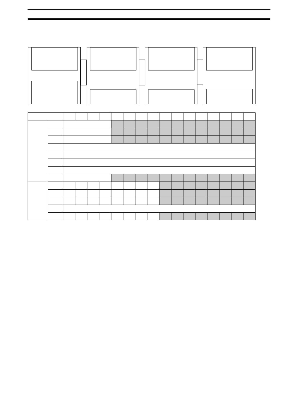
Example: Configuration Including Analog I/O Unit, Temperature Sensor Unit, and Expansion I/O Unit
CPU Unit
Analog I/O Unit
Temperature Sensor Unit
Expansion I/O Unit
(60 I/O points)
CPM1A-MAD01/11
CPM1A-TS001/101
(20 I/O points)
36 inputs
2 analog inputs
2 temperature inputs
16 inputs
IR 00000 to IR 00011
Input 0: IR 003
Input 0: IR 005
IR 00700 to IR 00711
IR 00100 to IR 00111
Input 1: IR 004
Input 1: IR 006
IR 00200 to IR 00211
24 outputs
IR 01000 to IR 01007
IR 01100 to IR 01107
1 analog output
No outputs
8 outputs
IR 01200 to IR 01207
Output 1: IR 013
IR 01400 to IR 01407
Bits
15
14
13
12
11
10
09
08
07
06
05
04
03
02
01
00
IR 000
Do not use
IR 001
Do not use
Inputs
IR 002
Do not use
IR 003
Used for input 0 of the Analog I/O Unit
IR 004
Used for input 1 of the Analog I/O Unit
IR 005
Used for input 0 of the Temperature Sensor Unit
IR 006
Used for input 1 of the Temperature Sensor Unit
IR 007
Do not use
IR 010
IR 011
Outputs
IR 012
IR 013
Used for the output of the Analog I/O Unit
IR 014
With the exception of CPM1A-TS002/102 Temperature Sensor Units, up to 3
Expansion Units (Analog I/O Units, Temperature Sensor Units, or CompoBus/S
Units) can be connected to a CPM1A or CPM2A PC. Only one
CPM1A-TS002/102 Temperature Sensor Unit can be connected. (See page
319 for an example of CPM1A-TS002/102 allocations.)
318
I/O Allocation for CPM2C PCs
Section
5-3
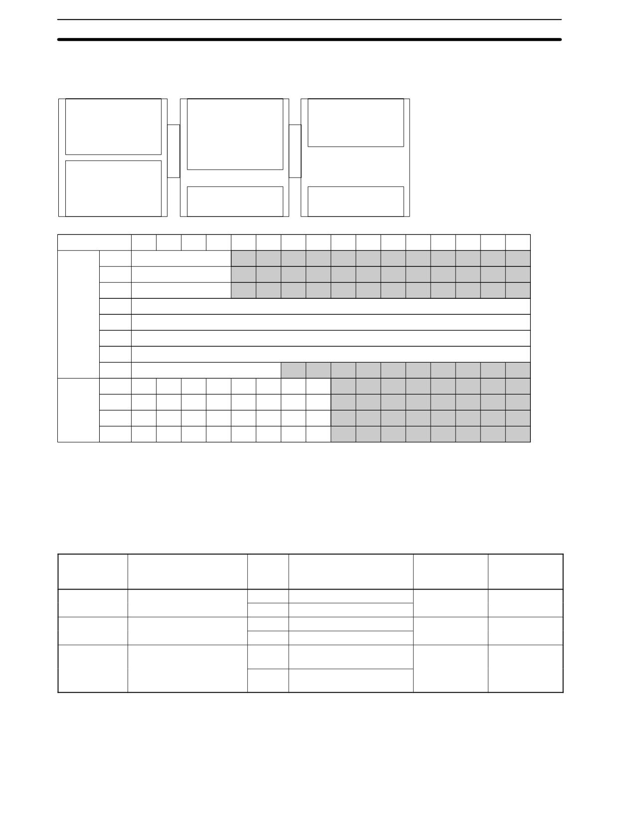
Example: Configuration Including Temperature Sensor Unit with 4 Inputs and CompoBus/S Link Unit
CPU Unit
Temperature Sensor Unit
CompoBus/S I/O Link Unit
(60 I/O points)
CPM1A-TS002/102
CPM1A-SRT21
36 inputs
2 temperature inputs
8 inputs
IR 00000 to IR 00011
Input 0: IR 003
IR 00700 to IR 00707
IR 00100 to IR 00111
Input 1: IR 004
IR 00200 to IR 00211
Input 2: IR 005
Input 3: IR 006
24 outputs
IR 01000 to IR 01007
IR 01100 to IR 01107
IR 01200 to IR 01207
8 outputs
No outputs
IR 01300 to IR 01307
Bits
15
14
13
12
11
10
09
08
07
06
05
04
03
02
01
00
IR 000
Do not use
IR 001
Do not use
Inputs
IR 002
Do not use
IR 003
Used for input 0 of the Temperature Sensor Unit
IR 004
Used for input 1 of the Temperature Sensor Unit
IR 005
Used for input 1 of the Temperature Sensor Unit
IR 006
Used for input 1 of the Temperature Sensor Unit
IR 007
Do not use
IR 010
IR 011
Outputs
IR 012
IR 013
Only one 4-input Temperature Sensor Unit (CPM1A-TS002/102) can be con-
nected to the PC. The CPM1A-TS002/102 can, however, be connected together
with an Expansion I/O Unit or a different Expansion Unit.
5-3
I/O Allocation for CPM2C PCs
5-3-1
CPU Units
No. of I/O
Model number
I/O
Allocated bits
Max. No. of
Max. No. of I/O
(on CPU Unit)
Expansion I/O
(see note 1)
Units
10
CPM2C-10CjDjjj-D
Inputs
6 inputs: 00000 to 00005
5
170
Outputs
4 outputs: 01000 to 01003
20
CPM2C-20CjDjjj-D
Inputs
12 inputs: 00000 to 00011
5
180
Outputs
8 outputs: 01000 to 01007
32
CPM2C-32CDTjj-D
Inputs
16 inputs: 00000 to 00007
5
192
and 00100 to 00107
Outputs
16 outputs: 01000 to 01007
and 01100 to 01107
Note
1. The values for the maximum number of I/O in the above table include the I/O
on Expansion I/O Units.
2. Although only up to 5 Expansion Units or Expansion I/O Units can be con-
nected to a CPM2C PC, no more than 10 input words and 10 output words
can be allocated.
319
I/O Allocation for CPM2C PCs
Section
5-3
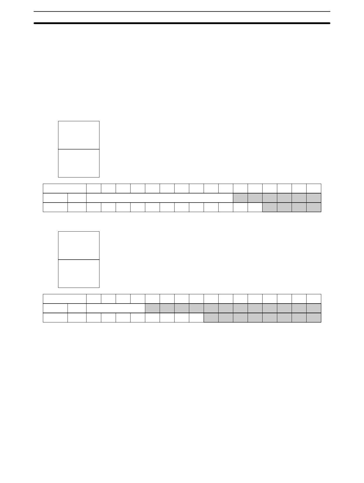
CPU Unit Allocation
• In the following diagrams, shaded areas indicate bits actually used for inputs or
outputs.
• Input bits are allocated starting from IR 00000.
• Output bits are allocated starting from IR 01000.
• Bits in the output words that are not used as output bits can be used as work
bits.
• Bits in the input words that are not used as input bits cannot be used as work
bits.
CPU Units with 10 I/O Points
6 inputs
CPM2C-10CjDjj-j
IR 00000
to
IR 00005
4 outputs
IR 01000
to
IR 01003
Bits
15
14
13
12
11
10
09
08
07
06
05
04
03
02
01
00
Inputs
IR 000
Do not use
Outputs
IR 010
CPU Units with 20 I/O Points
12 inputs
CPM2C-20CjDjj-j
IR 00000
to
IR 00011
8 outputs
IR 01000
to
IR 01007
Bits
15
14
13
12
11
10
09
08
07
06
05
04
03
02
01
00
Inputs
IR 000
Do not use
Outputs
IR 010
320
I/O Allocation for CPM2C PCs
Section
5-3
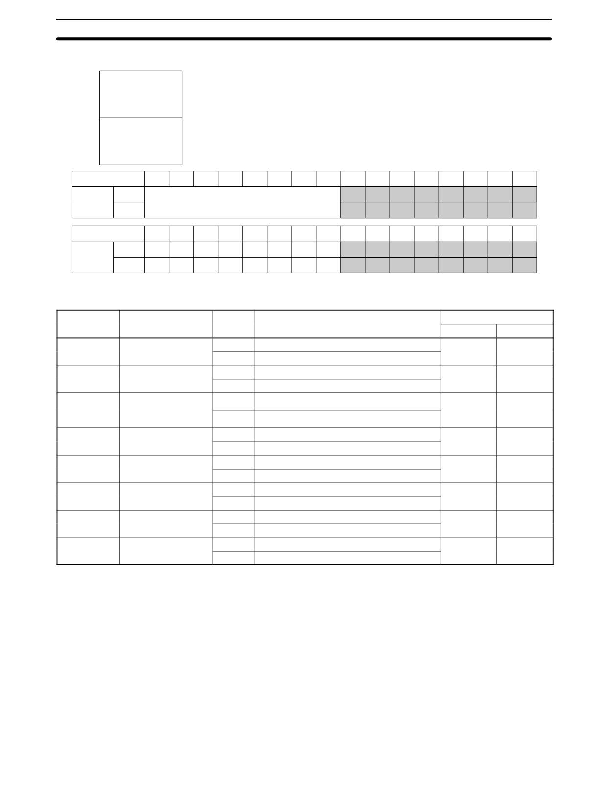
CPU Units with 32 I/O Points
16 inputs
CPM2C-32CDTjj-D
IR 00000 to IR 00007
and
IR 00100 to IR 00107
16 outputs
IR 01000 to IR 01007
and
IR 01100 to IR 01107
Bits
15
14
13
12
11
10
09
08
07
06
05
04
03
02
01
00
Inputs
IR 000
Do not use
IR 001
Bits
15
14
13
12
11
10
09
08
07
06
05
04
03
02
01
00
Outputs
IR 010
IR 011
5-3-2
Expansion I/O Units
No. of I/O
Model number
I/O
Allocated bits
Max. No. of Units
CPM2C
CPM2C-S
8
CPM2C-8EDj
Input
8 inputs: Word (m+1), bits 00 to 07
5
3
Output
---
16
CPM2C-16EDj
Input
16 inputs: Word (m+1), bits 00 to 15
5
3
Output
---
8
CPM2C-8ER
Input
---
5
3
CPM2C-8ETj
CPM2C-8ET1j
Output
8 outputs: Word (n+1), bits 00 to 07
16
CPM2C-16ETj
Input
---
5
3
CPM2C-16ET1j
Output
16 outputs: Word (n+1), bits 00 to 15
10
CPM2C-10EDR
Input
6 inputs: Word (m+1), bits 00 to 05
5
3
Output
4 outputs: Word (n+1), bits 00 to 03
20
CPM2C-20EDR
Input
12 inputs: Word (m+1), bits 00 to 11
5
3
Output
8 outputs: Word (n+1), bits 00 to 07
24
CPM2C-24EDTj
Input
16 inputs: Word (m+1), bits 00 to 15
5
3
CPM2C-24EDT1j
Output
8 outputs: Word (n+1), bits 00 to 07
32
CPM2C-32EDTj
Input
16 inputs: Word (m+1), bits 00 to 15
5
3
CPM2C-32EDT1j
Output
16 outputs: Word (n+1), bits 00 to 15
Note m: “m” denotes the last input word allocated to the CPU Unit, or to the previous
Expansion Unit or Expansion I/O Unit if one is already connected.
n: “n” denotes the last output word allocated to the CPU Unit, or to the previous
Expansion Unit or Expansion I/O Unit if one is already connected.
Expansion I/O Unit Allocation
• In the following diagrams, shaded areas indicate bits actually used for inputs or
outputs.
• Input bits are allocated to Expansion I/O Units starting from word (m+1), where
“m” is the last input word allocated to the CPU Unit, or to the previous Expan-
sion Unit or Expansion I/O Unit if one is already connected.
• Output bits are allocated to Expansion I/O Units starting from word (n+1),
where “n” is the last output word allocated to the CPU Unit, or to the previous
Expansion Unit or Expansion I/O Unit if one is already connected.
321
I/O Allocation for CPM2C PCs
Section
5-3
• Bits in the output words that are not used as output bits can be used as work
bits.
• Bits in the input words that are not used as input bits can be used as work bits.
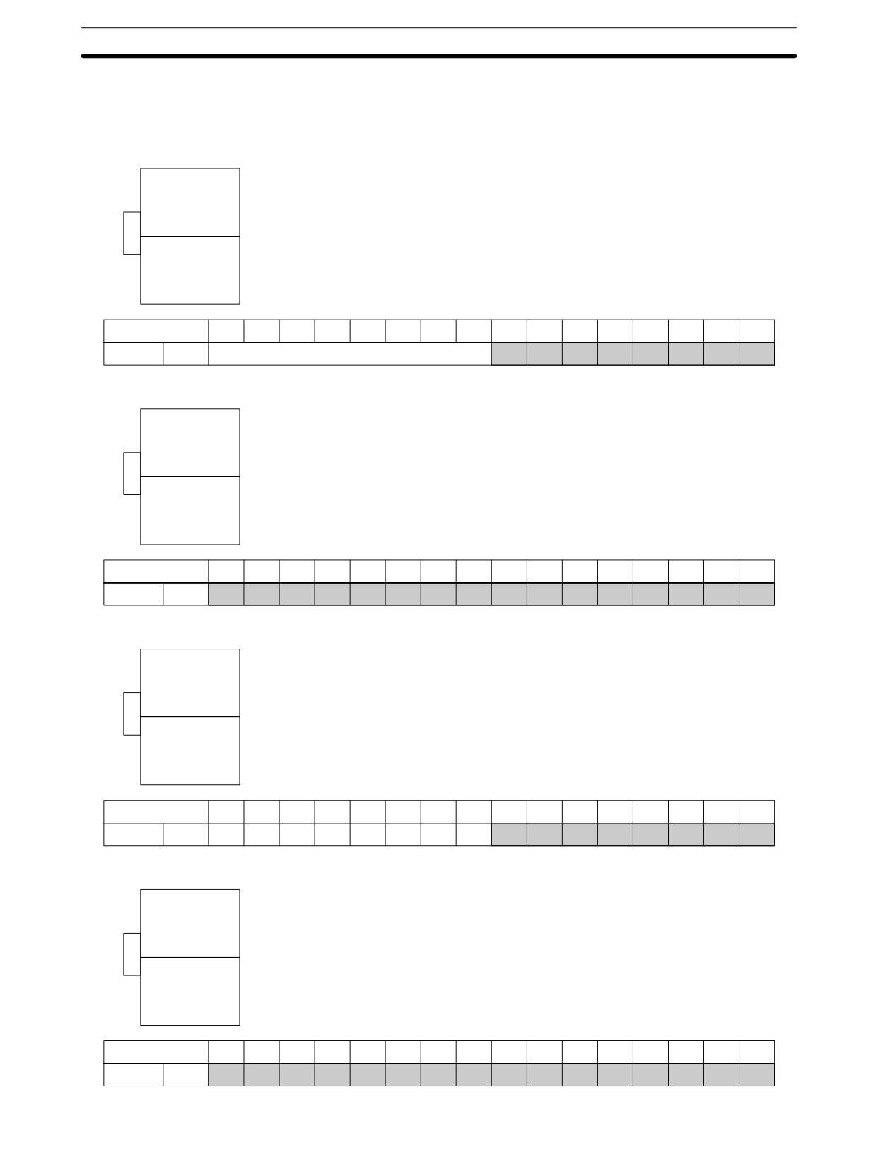
Expansion I/O Unit with 8 Inputs
8 inputs
CPM2C-8EDC
Word (m+1), bit 00
CPM2C-8EDM
to
Word (m+1), bit 07
No outputs
Bits
15
14
13
12
11
10
09
08
07
06
05
04
03
02
01
00
Inputs
m+1
Do not use
Expansion I/O Unit with 16 Inputs
16 inputs
CPM2C-16EDC
Word (m+1), bit 00
CPM2C-16EDM
to
Word (m+1), bit 15
No outputs
Bits
15
14
13
12
11
10
09
08
07
06
05
04
03
02
01
00
Inputs
m+1
Expansion I/O Units with 8 Outputs
CPM2C-8ER
No inputs
CPM2C-8ETC
CPM2C-8ET1C
CPM2C-8ETM
CPM2C-8ET1M
8 outputs
Word (n+1), bit 00
to
Word (n+1), bit 07
Bits
15
14
13
12
11
10
09
08
07
06
05
04
03
02
01
00
Outputs
n+1
Expansion I/O Units with 16 Outputs
CPM2C-16ETC
No inputs
CPM2C-16ET1C
CPM2C-16ETM
CPM2C-16ET1M
16 outputs
Word (n+1), bit 00
to
Word (n+1), bit 15
Bits
15
14
13
12
11
10
09
08
07
06
05
04
03
02
01
00
Outputs
n+1
322
I/O Allocation for CPM2C PCs
Section
5-3
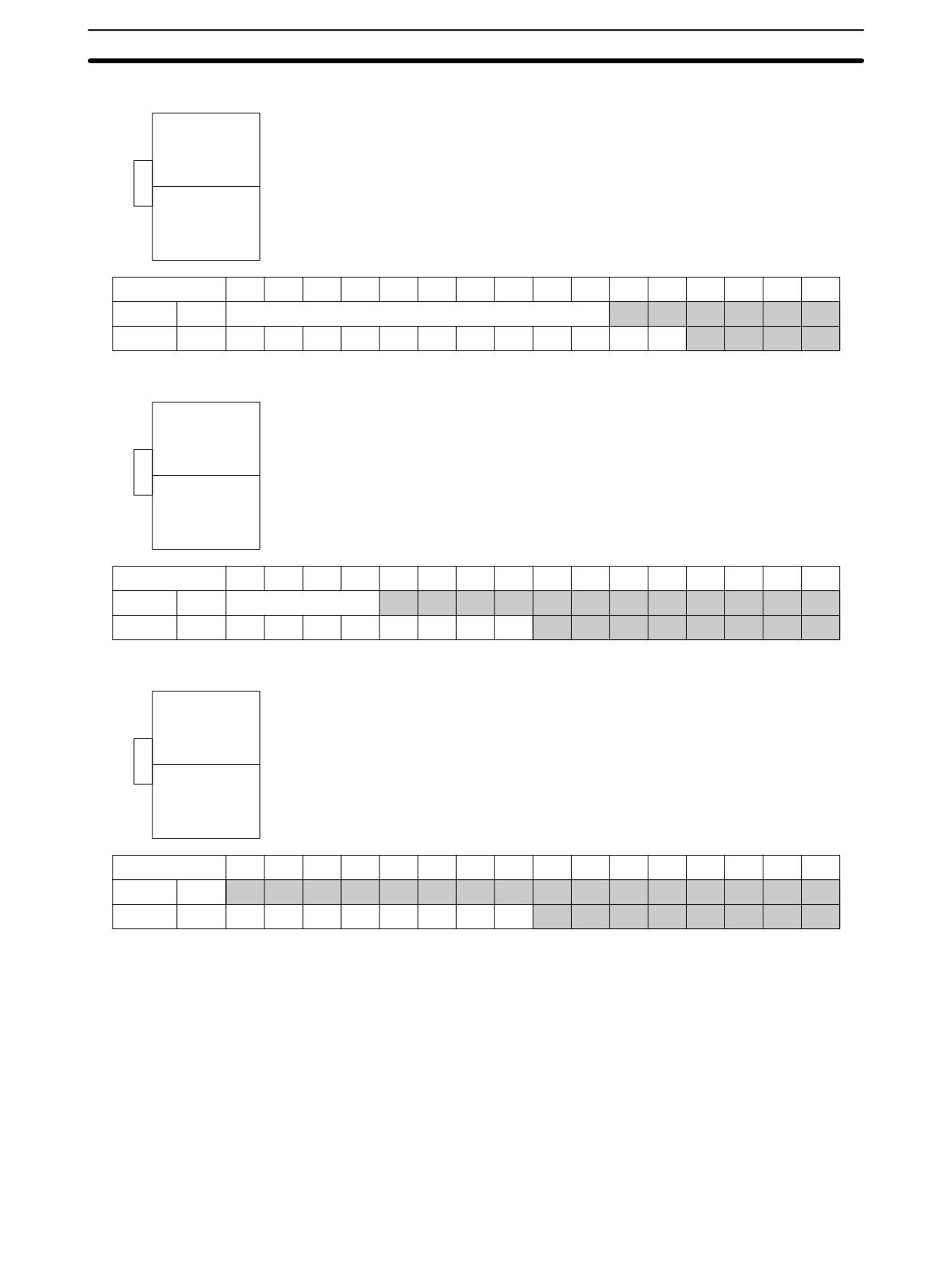
Expansion I/O Unit with 10 I/O Points
6 inputs
CPM2C-10EDR
Word (m+1), bit 00
to
Word (m+1), bit 05
4 outputs
Word (n+1), bit 00
to
Word (n+1), bit 03
Bits
15
14
13
12
11
10
09
08
07
06
05
04
03
02
01
00
Inputs
m+1
Do not use
Outputs
n+1
Expansion I/O Unit with 20 I/O Points
12 inputs
CPM2C-20EDR
Word (m+1), bit 00
to
Word (m+1), bit 11
8 outputs
Word (n+1), bit 00
to
Word (n+1), bit 07
Bits
15
14
13
12
11
10
09
08
07
06
05
04
03
02
01
00
Inputs
m+1
Do not use
Outputs
n+1
Expansion I/O Units with 24 I/O Points
16 inputs
CPM2C-24EDTC
Word (m+1), bit 00
CPM2C-24EDT1C
to
CPM2C-24EDTM
Word (m+1), bit 15
CPM2C-24EDT1M
8 outputs
Word (n+1), bit 00
to
Word (n+1), bit 07
Bits
15
14
13
12
11
10
09
08
07
06
05
04
03
02
01
00
Inputs
m+1
Outputs
n+1
323
I/O Allocation for CPM2C PCs
Section
5-3
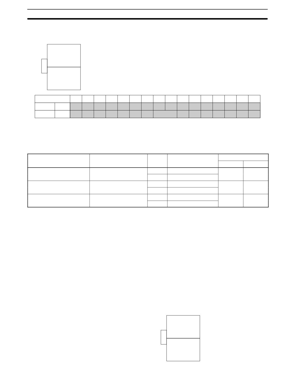
Expansion I/O Units with 32 I/O Points
16 inputs
CPM2C-32EDTC
Word (m+1), bit 00
CPM2C-32EDT1C
to
CPM2C-32EDTM
Word (m+1), bit 15
CPM2C-32EDT1M
16 outputs
Word (n+1), bit 00
to
Word (n+1), bit 15
Bits
15
14
13
12
11
10
09
08
07
06
05
04
03
02
01
00
Inputs
m+1
Outputs
n+1
5-3-3
Expansion Units
Unit
Model number
I/O
Allocated words
Max. No. of Units
CPM2C
CPM2C-S
Analog I/O Unit
CPM2C-MAD11
Input
2 inputs: m+1, m+2
4
3
Output
1 output: n+1
Temperature Sensor Unit
CPM2C-TS001
Input
2 inputs: m+1, m+2
4
3
CPM2C-TS 101
Output
---
CompoBus/S I/O Link Unit
CPM2C-SRT21
Input
1 input: m+1
5
3
Output
1 output: n+1
Note
1. m: “m” denotes the last input word allocated to the CPU Unit, or to the pre-
vious Expansion Unit or Expansion I/O Unit if one is already connected.
n: “n” denotes the last output word allocated to the CPU Unit, or to the pre-
vious Expansion Unit or Expansion I/O Unit if one is already connected.
2. Because the CPM2C-MAD11 Analog I/O Unit and the CPM2C-TS001/101
Temperature Sensor Units require 2 I/O words each, only 4 of these Units
can be connected to the PC. (The CPU Unit itself requires one input word
and one output word.) A different Unit, such as an Expansion I/O Unit or the
CPM2C-SRT21 CompoBus/S I/O Link Unit, can, however, be connected in
addition to 4 Analog I/O Units or Temperature Sensor Units.
Analog I/O Unit
CPM2C-MAD11
2 analog inputs
Input 0: word (m+1)
Input 1: word (m+2)
1 analog output
Output 0: word (n+1)
324
I/O Allocation for CPM2C PCs
Section
5-3
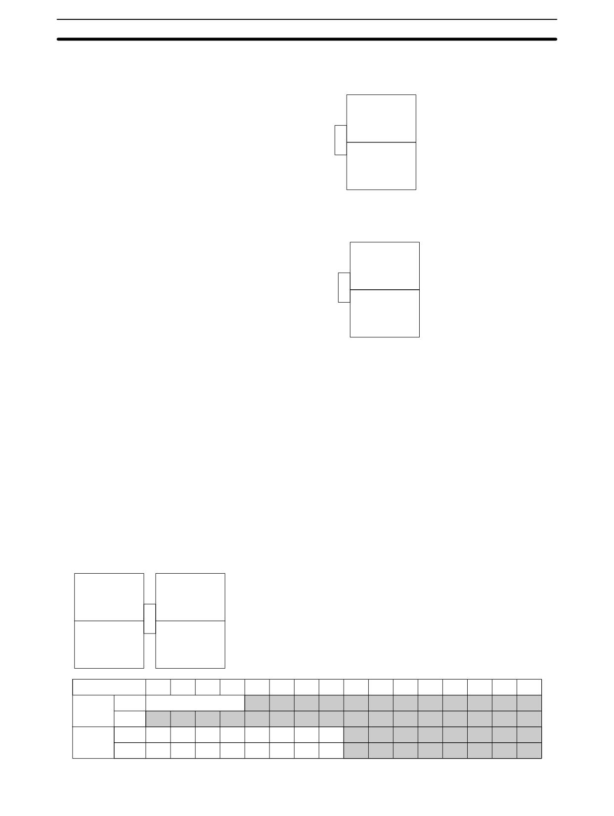
Temperature Sensor Units
CPM2C-TS001/TS101
2 temperature inputs
Input 0: word (m+1)
Input 1: word (m+2)
No outputs
CompoBus/S I/O Link Unit
CPM2C-SRT21
8 inputs
Input: word (m+1)
8 outputs
Output: word (n+1)
Note Input bits 00 to 07 in word (m+1) are for outputs from the Master. Output bits 00 to
07 in word (n+1), are for inputs to the Master.
5-3-4
Examples of Expansion Unit and Expansion I/O Unit Allocation
Up to 5 Expansion Units or Expansion I/O Units can be connected to a CPM2C
PC. Input bits and output bits are automatically allocated starting from the CPU
Unit and continuing through Expansion Units and Expansion I/O Units in the
order in which they are connected. The input area consists of the 10 words from
IR 000 to 009, and the output area consists of the 10 words from IR 010 to 019.
Although I/O bits are allocated automatically, it is necessary to ensure that both
the number of input words and the number of output words do not exceed 10. For
example, the Analog I/O Unit and Temperature Sensor Unit require 2 input
words and so it is not possible to connect 5 of these Units.
Example: CPU Unit with 20 I/O Points + Expansion I/O Unit with 24 I/O Points
CPU Unit
Expansion I/O Unit
(20 I/O points)
(24 I/O points)
12 inputs
16 inputs
IR 00000
IR 00100
to
to
IR 00011
IR 00115
8 outputs
8 outputs
IR 01000
IR 01100
to
to
IR 01007
IR 01107
Bits
15
14
13
12
11
10
09
08
07
06
05
04
03
02
01
00
IR 000
Do not use
Inputs
IR 001
IR 010
Outputs
IR 011
325
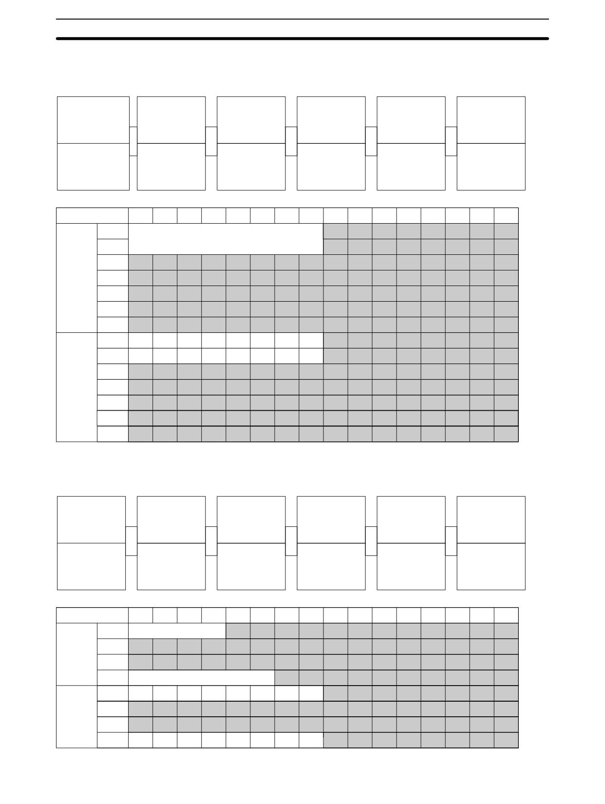
I/O Allocation for CPM2C PCs
Section
5-3
Example: CPU Unit with 32 I/O Points + 5 Expansion I/O Units with 32 I/O Points
CPU Unit
Expansion I/O Unit
Expansion I/O Unit
Expansion I/O Unit
Expansion I/O Unit
Expansion I/O Unit
(32 I/O points)
(32 I/O points)
(32 I/O points)
(32 I/O points)
(32 I/O points)
(32 I/O points)
16 inputs
16 inputs
16 inputs
16 inputs
16 inputs
16 inputs
IR 00000 to IR 00007
IR 00200
IR 00300
IR 00400
IR 00500
IR 00600
and
to
to
to
to
to
IR 00100 to IR 00107
IR 00215
IR 00315
IR 00415
IR 00515
IR 00615
16 outputs
16 outputs
16 outputs
16 outputs
16 outputs
16 outputs
IR 01000 to IR 01007
IR 01200
IR 01300
IR 01400
IR 01500
IR 01600
and
to
to
to
to
to
IR 01100 to IR 01107
IR 01215
IR 012315
IR 01415
IR 01515
IR 01615
Bits
15
14
13
12
11
10
09
08
07
06
05
04
03
02
01
00
IR 000
Do not use
IR 001
Inputs
IR 002
IR 003
IR 004
IR 005
IR 006
IR 010
Outputs
IR 011
IR 012
IR 013
IR 014
IR 015
IR 016
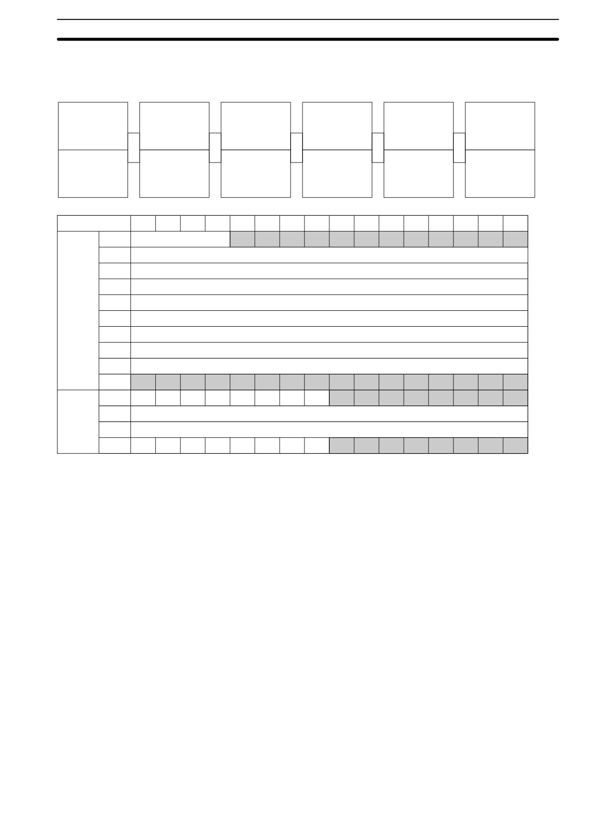
Example: Configuration Including Expansion I/O Units and a CompoBus/S I/O Link Unit
CPU Unit
Expansion I/O Unit
Expansion I/O Unit
Expansion I/O Unit
Expansion I/O Unit
CompoBus/S I/O
(20 I/O points)
(16 input points)
(16 input points)
(16 output points)
(16 output points)
Link Unit
12 inputs
16 inputs
16 inputs
8 inputs
IR 00000
IR 00100
IR 00200
No inputs
No inputs
IR 00300
to
to
to
to
IR 00011
IR 00115
IR 00215
IR 00307
8 outputs
16 outputs
16 outputs
8 outputs
IR 01000
No outputs
No outputs
IR 01100
IR 01200
IR 01300
to
to
to
to
IR 01007
IR 01115
IR 01215
IR 01307
Bits
15
14
13
12
11
10
09
08
07
06
05
04
03
02
01
00
IR 000
Do not use
IR 001
Inputs
IR 002
IR 003
Do not use
IR 010
IR 011
Outputs
IR 012
IR 013
326
I/O Allocation for CPM2C PCs
Section
5-3
Example: Configuration Including Analog I/O Units, Temperature Sensor Units, and Expansion I/O Unit
CPU Unit
Analog I/O Unit 1
Temperature Sensor
Analog I/O Unit 2
Temperature Sensor
Expansion I/O Unit
(20 I/O points)
CPM2C-MAD11
Unit 1
CPM2C-MAD11
Unit 2
(24 I/O points)
CPM2C-TS001
CPM2C-TS101
12 inputs
2 analog inputs
2 temperature inputs
2 analog inputs
2 temperature inputs
16 inputs
IR 00000
Input 0: IR 001
Input 0: IR 003
Input 0: IR 005
Input 0: IR 007
IR 00900
to
Input 1: IR 002
Input 1: IR 004
Input 1: IR 006
Input 1: IR 008
to
IR 00011
IR 00915
8 outputs
1 analog output
1 analog output
8 outputs
IR 01000
Output: IR 011
Output: word 012
IR 01300
to
No outputs
No outputs
to
IR 01007
IR 01307
Bits
15
14
13
12
11
10
09
08
07
06
05
04
03
02
01
00
IR 000
Do not use
IR 001
Used for input 0 of Analog I/O Unit 1
IR 002
Used for input 1 of Analog I/O Unit 1
IR 003
Used for input 0 of Temperature Sensor Unit 1
IR 004
Used for input 1 of Temperature Sensor Unit 1
Inputs
IR 005
Used for input 0 of Analog I/O Unit 2
IR 006
Used for input 1 of Analog I/O Unit 2
IR 007
Used for input 0 of Temperature Sensor Unit 2
IR 008
Used for input 1 of Temperature Sensor Unit 2
IR 009
IR 010
IR 011
Used for the output of Analog I/O Unit 1
Outputs
IR 012
Used for the output of Analog I/O Unit 2
IR 013
327
SECTION 6
Ladder-diagram Programming
This section explains the basic steps and concepts involved in writing a basic ladder diagram program. It introduces the
instructions that are used to build the basic structure of the ladder diagram and control its execution. The entire set of instruc-
tions used in programming is described in Section 7 Instruction Set.
6-1
Basic Procedure
330
6-2
Instruction Terminology
330
6-3
Basic Ladder Diagrams
331
6-3-1
Basic Terms
331
6-3-2
Mnemonic Code
332
6-3-3
Ladder Instructions
333
6-3-4
OUTPUT and OUTPUT NOT
336
6-3-5
The END Instruction
337
6-3-6
Logic Block Instructions
337
6-3-7
Coding Multiple Right-hand Instructions
345
6-3-8
Branching Instruction Lines
345
6-3-9
Jumps
349
6-4
Controlling Bit Status
350
6-4-1
SET and RESET
350
6-4-2
DIFFERENTIATE UP and DIFFERENTIATE DOWN
351
6-4-3
KEEP
351
6-4-4
Self-maintaining Bits (Seal)
352
6-5
Work Bits (Internal Relays)
352
6-6
Programming Precautions
354
6-7
Program Execution
356
329
Instruction Terminology
Section
6-2
6-1
Basic Procedure
There are several basic steps involved in writing a program. Sheets that can be
copied to aid in programming are provided in Appendix D I/O Assignment Sheet
and Appendix E Program Coding Sheet.
1, 2, 3...
1.
Obtain a list of all I/O devices and the I/O points that have been assigned to
them and prepare a table that shows the I/O bit allocated to each I/O device.
2.
If you are using LR bits to link two PCs, prepare sheet showing the used of
these bits.
3.
Determine what words are available for work bits and prepare a table in
which you can allocate these as you use them.
4.
Also prepare tables of TC numbers and jump numbers so that you can allo-
cate these as you use them. Remember, the function of a TC number can
be defined only once within the program; jump numbers 01 through 99 can
be used only once each. (TC number are described in 7-15 Timer and
Counter Instructions; jump numbers are described later in this section.)
5.
Draw the ladder diagram.
6.
Input the program into the CPU Unit. When using the Programming Con-
sole, this will involve converting the program to mnemonic form.
7.
Check the program for syntax errors and correct these.
8.
Execute the program to check for execution errors and correct these.
9.
After the entire Control System has been installed and is ready for use,
execute the program and fine tune it if required.
The basics of ladder-diagram programming and conversion to mnemonic code
are described in 6-3 Basic Ladder Diagrams. Preparing for and inputting the pro-
gram via the Programming Console are described in the CPM1 Operation
Manual, the CPM1A Operation Manual, the CPM2A Operation Manual, the
CPM2C Operation Manual, and the SRM1 Master Control Units Manual and via
the SSS in the SSS Operation Manual: C-series PCs.
The rest of Section 6 covers more advanced programming, programming pre-
cautions, and program execution. All special application instructions are cov-
ered in Section 7 Instruction Set. Debugging is described in the CPM1 Operation
Manual, the CPM1A Operation Manual, the CPM2A Operation Manual, the
CPM2C Operation Manual, the SRM1 Master Control Units Manual, and SSS
Operation Manual: C-series PCs. Section 9 Troubleshooting also provides in-
formation required for debugging.
6-2
Instruction Terminology
There are basically two types of instructions used in ladder-diagram program-
ming: instructions that correspond to the conditions on the ladder diagram and
are used in instruction form only when converting a program to mnemonic code
and instructions that are used on the right side of the ladder diagram and are
executed according to the conditions on the instruction lines leading to them.
Most instructions have at least one or more operands associated with them. Op-
erands indicate or provide the data on which an instruction is to be performed.
These are sometimes input as the actual numeric values, but are usually the ad-
dresses of data area words or bits that contain the data to be used. For instance,
a MOVE instruction that has IR 000 designated as the source operand will move
the contents of IR 000 to some other location. The other location is also desig-
nated as an operand. A bit whose address is designated as an operand is called
an operand bit; a word whose address is designated as an operand is called an
operand word. If the actual value is entered as a constant, it is preceded by # to
indicate that it is not an address.
330
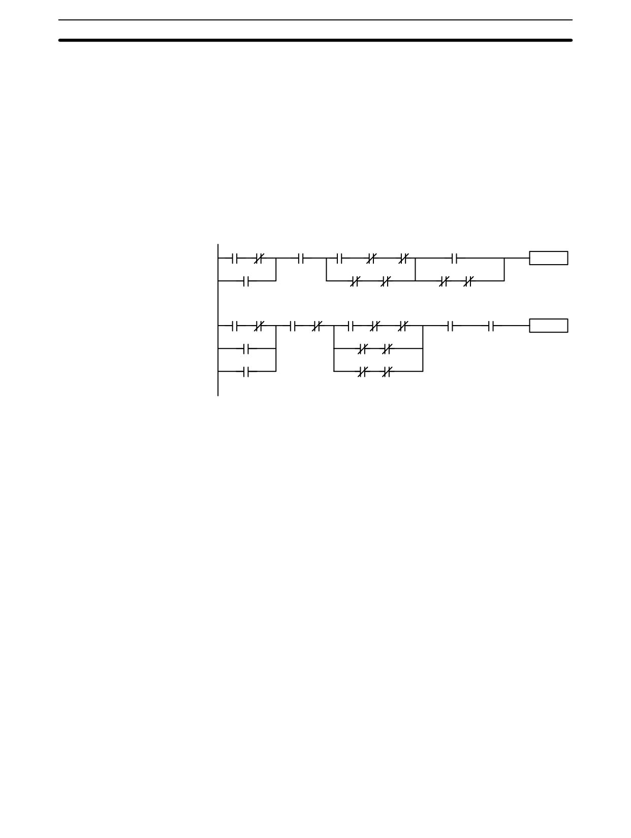
Basic Ladder Diagrams
Section
6-3
Other terms used in describing instructions are introduced in Section 7 Instruc-
tion Set.
6-3
Basic Ladder Diagrams
A ladder diagram consists of one line running down the left side with lines
branching off to the right. The line on the left is called the bus bar; the branching
lines, instruction lines or rungs. Along the instruction lines are placed conditions
that lead to other instructions on the right side. The logical combinations of these
conditions determine when and how the instructions at the right are executed. A
ladder diagram is shown below.
00000
20000
25208
HR 0109
LR 0003
20001
20002
Instruction
00001
00501
00502
00503
00504
00100
00002
00003 HR 0050
00007 TIM 001 LR 0515
00403
00405
Instruction
00010
21001
21002
00011
21005
21007
As shown in the diagram above, instruction lines can branch apart and they can
join back together. The vertical pairs of lines are called conditions. Conditions
without diagonal lines through them are called normally open conditions and
correspond to a LOAD, AND, or OR instruction. The conditions with diagonal
lines through them are called normally closed conditions and correspond to a
LOAD NOT, AND NOT, or OR NOT instruction. The number above each condi-
tion indicates the operand bit for the instruction. It is the status of the bit
associated with each condition that determines the execution condition for fol-
lowing instructions. The way the operation of each of the instructions corre-
sponds to a condition is described below. Before we consider these, however,
there are some basic terms that must be explained.
Note When displaying ladder diagrams with the SSS, a second bus bar will be shown
on the right side of the ladder diagram and will be connected to all instructions on
the right side. This does not change the ladder-diagram program in any function-
al sense. No conditions can be placed between the instructions on the right side
and the right bus bar, i.e., all instructions on the right must be connected directly
to the right bus bar. Refer to the SSS Operation Manual: C-series PCs for details.
6-3-1
Basic Terms
Normally Open and
Each condition in a ladder diagram is either ON or OFF depending on the status
Normally Closed
of the operand bit that has been assigned to it. A normally open condition is ON if
Conditions
the operand bit is ON; OFF if the operand bit is OFF. A normally closed condition
is ON if the operand bit is OFF; OFF if the operand bit is ON. Generally speaking,
you use a normally open condition when you want something to happen when a
331
Basic Ladder Diagrams
Section
6-3
bit is ON, and a normally closed condition when you want something to happen
when a bit is OFF.
00000
Instruction is executed
Instruction
when IR bit 00000 is ON.
Normally open
condition
00000
Instruction is executed
Instruction
when IR bit 00000 is OFF.
Normally closed
condition
In ladder diagram programming, the logical combination of ON and OFF condi-
Execution Conditions
tions before an instruction determines the compound condition under which the
instruction is executed. This condition, which is either ON or OFF, is called the
execution condition for the instruction. All instructions other than LOAD instruc-
tions have execution conditions.
The operands designated for any of the ladder instructions can be any bit in the
Operand Bits
IR, SR, HR, AR, LR, or TC areas. This means that the conditions in a ladder dia-
gram can be determined by I/O bits, flags, work bits, timers/counters, etc. LOAD
and OUTPUT instructions can also use TR area bits, but they do so only in spe-
cial applications. Refer to 6-3-8 Branching Instruction Lines for details.
The way that conditions correspond to what instructions is determined by the
Logic Blocks
relationship between the conditions within the instruction lines that connect
them. Any group of conditions that go together to create a logic result is called a
logic block. Although ladder diagrams can be written without actually analyzing
individual logic blocks, understanding logic blocks is necessary for efficient pro-
gramming and is essential when programs are to be input in mnemonic code.
An instruction block consists of all the instructions that are interconnected
Instruction Block
across the ladder diagram. One instruction block thus consists of all the instruc-
tions between where you can draw a horizontal line across the ladder diagram
without intersecting any vertical lines and the next place where you can draw the
same type of horizontal line.
6-3-2
Mnemonic Code
The ladder diagram cannot be directly input into the PC via a Programming Con-
sole; the SSS is required. To input from a Programming Console, it is necessary
to convert the ladder diagram to mnemonic code. The mnemonic code provides
exactly the same information as the ladder diagram, but in a form that can be
typed directly into the PC. Actually you can program directly in mnemonic code,
although it in not recommended for beginners or for complex programs. Also,
regardless of the Programming Device used, the program is stored in memory in
mnemonic form, making it important to understand mnemonic code.
Because of the importance of the Programming Console as a Programming De-
vice and because of the importance of mnemonic code in complete understand-
ing of a program, we will introduce and describe the mnemonic code along with
the ladder diagram. Remember, you will not need to use the mnemonic code if
you are inputting via the SSS (although you can use it with the SSS if you prefer).
The program is input into addresses in Program Memory. Addresses in Program
Program Memory Structure
Memory are slightly different to those in other memory areas because each ad-
dress does not necessarily hold the same amount of data. Rather, each address
holds one instruction and all of the definers and operands (described in more
332

Basic Ladder Diagrams
Section
6-3
detail later) required for that instruction. Because some instructions require no
operands, while others require up to three operands, Program Memory address-
es can be from one to four words long.
Program Memory addresses start at 00000 and run until the capacity of Program
Memory has been exhausted. The first word at each address defines the instruc-
tion. Any definers used by the instruction are also contained in the first word.
Also, if an instruction requires only a single bit operand (with no definer), the bit
operand is also programmed on the same line as the instruction. The rest of the
words required by an instruction contain the operands that specify what data is
to be used. When converting to mnemonic code, all but ladder diagram instruc-
tions are written in the same form, one word to a line, just as they appear in the
ladder diagram symbols. An example of mnemonic code is shown below. The
instructions used in it are described later in the manual.
Address
Instruction
Operands
00000
LD
HR
0001
00001
AND
00001
00002
OR
00002
00003
LD NOT
00100
00004
OR
00101
00005
AND LD
00006
MOV(21)
000
DM
0000
00007
CMP(20)
DM
0000
HR
00
00008
AND
25505
00009
OUT
20000
00010
MOV(21)
DM
0000
DM
0500
00011
LD
00502
00012
AND
00005
00013
OUT
20001
The address and instruction columns of the mnemonic code table are filled in for
the instruction word only. For all other lines, the left two columns are left blank. If
the instruction requires no definer or bit operand, the operand column is left
blank for first line. It is a good idea to cross through any blank data column
spaces (for all instruction words that do not require data) so that the data column
can be quickly scanned to see if any addresses have been left out.
When programming, addresses are automatically displayed and do not have to
be input unless for some reason a different location is desired for the instruction.
When converting to mnemonic code, it is best to start at Program Memory ad-
dress 00000 unless there is a specific reason for starting elsewhere.
6-3-3
Ladder Instructions
The ladder instructions are those instructions that correspond to the conditions
on the ladder diagram. Ladder instructions, either independently or in combina-
tion with the logic block instructions described next, form the execution condi-
tions upon which the execution of all other instructions are based.
333
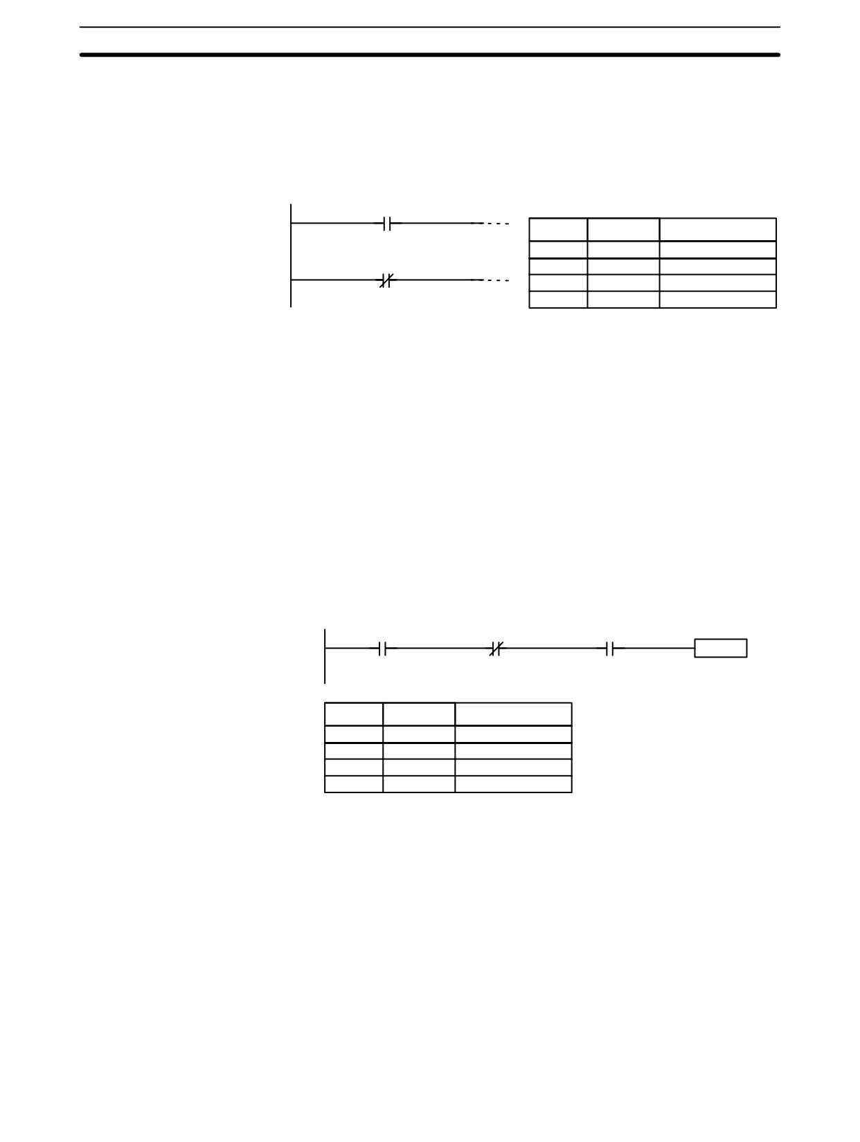
Basic Ladder Diagrams
Section
6-3
The first condition that starts any logic block within a ladder diagram corre-
LOAD and LOAD NOT
sponds to a LOAD or LOAD NOT instruction. Each of these instruction requires
one line of mnemonic code. “Instruction” is used as a dummy instruction in the
following examples and could be any of the right-hand instructions described lat-
er in this manual.
00000
Address
Instruction
Operands
A LOAD instruction.
00000
LD
00000
00000
00001
Instruction
00002
LD NOT
00000
A LOAD NOT instruction.
00003
Instruction
When this is the only condition on the instruction line, the execution condition for
the instruction at the right is ON when the condition is ON. For the LOAD instruc-
tion (i.e., a normally open condition), the execution condition would be ON when
IR 00000 was ON; for the LOAD NOT instruction (i.e., a normally closed condi-
tion), it would be ON when 00000 was OFF.
When two or more conditions lie in series on the same instruction line, the first
AND and AND NOT
one corresponds to a LOAD or LOAD NOT instruction; and the rest of the condi-
tions, to AND or AND NOT instructions. The following example shows three
conditions which correspond in order from the left to a LOAD, an AND NOT, and
an AND instruction. Again, each of these instructions requires one line of mne-
monic code.
00000
00100
LR 0000
Instruction
Address
Instruction
Operands
00000
LD
00000
00001
AND NOT
00100
00002
AND
LR
0000
00003
Instruction
The instruction would have an ON execution condition only when all three condi-
tions are ON, i.e., when IR 00000 was ON, IR 00100 was OFF, and LR 0000 was
ON.
AND instructions in series can be considered individually, with each taking the
logical AND of the execution condition (i.e., the total of all conditions up to that
point) and the status of the AND instruction’s operand bit. If both of these are ON,
an ON execution condition will be produced for the next instruction. If either is
OFF, the result will also be OFF. The execution condition for the first AND
instruction in a series is the first condition on the instruction line.
Each AND NOT instruction in a series would take the logical AND between its
execution condition and the inverse of its operand bit.
334
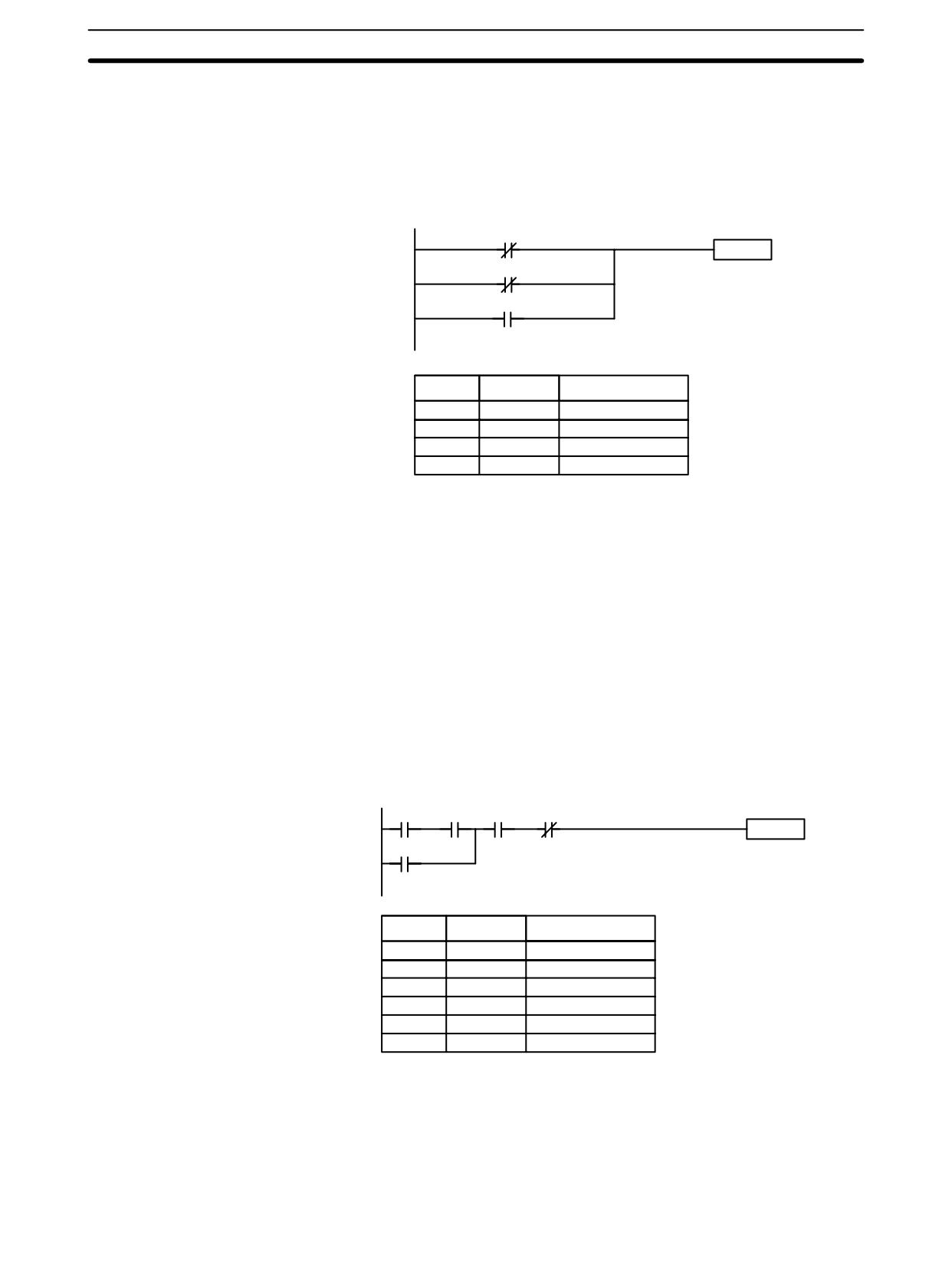
Basic Ladder Diagrams
Section
6-3
When two or more conditions lie on separate instruction lines running in parallel
OR and OR NOT
and then joining together, the first condition corresponds to a LOAD or LOAD
NOT instruction; the rest of the conditions correspond to OR or OR NOT instruc-
tions. The following example shows three conditions which correspond in order
from the top to a LOAD NOT, an OR NOT, and an OR instruction. Again, each of
these instructions requires one line of mnemonic code.
00000
Instruction
00100
LR 0000
Address
Instruction
Operands
00000
LD NOT
00000
00001
OR NOT
00100
00002
OR
LR
0000
00003
Instruction
The instruction would have an ON execution condition when any one of the three
conditions was ON, i.e., when IR 00000 was OFF, when IR 00100 was OFF, or
when LR 0000 was ON.
OR and OR NOT instructions can be considered individually, each taking the
logical OR between its execution condition and the status of the OR instruction’s
operand bit. If either one of these were ON, an ON execution condition would be
produced for the next instruction.
Combining AND and OR
When AND and OR instructions are combined in more complicated diagrams,
Instructions
they can sometimes be considered individually, with each instruction performing
a logic operation on the execution condition and the status of the operand bit.
The following is one example. Study this example until you are convinced that
the mnemonic code follows the same logic flow as the ladder diagram.
00000
00001
00002
00003
Instruction
00200
Address
Instruction
Operands
00000
LD
00000
00001
AND
00001
00002
OR
00200
00003
AND
00002
00004
AND NOT
00003
00005
Instruction
Here, an AND is taken between the status of IR 00000 and that of IR 00001 to
determine the execution condition for an OR with the status of IR 00200. The
result of this operation determines the execution condition for an AND with the
status of IR 00002, which in turn determines the execution condition for an AND
with the inverse (i.e., and AND NOT) of the status of IR 00003.
335
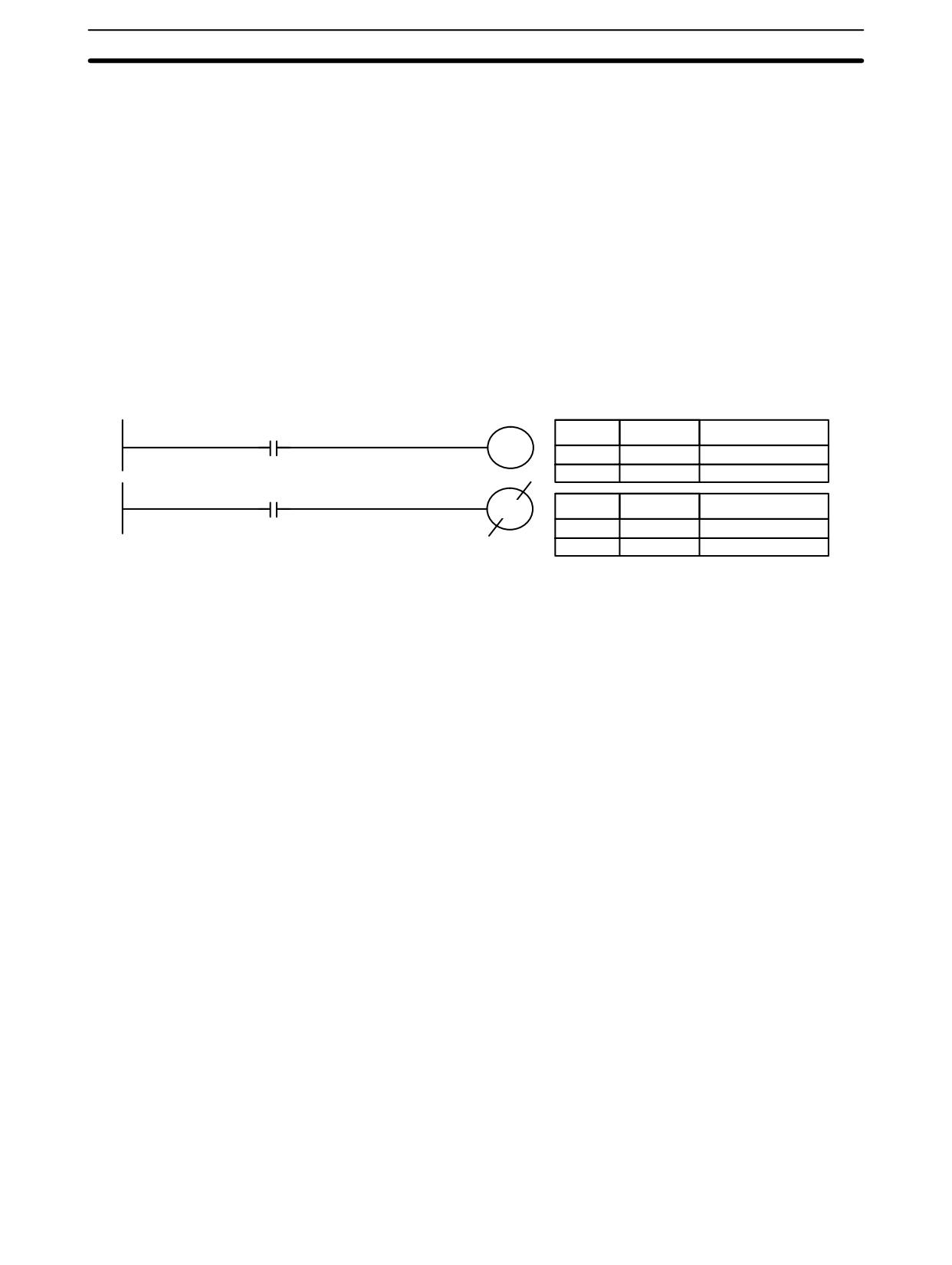
Basic Ladder Diagrams
Section
6-3
In more complicated diagrams, however, it is necessary to consider logic blocks
before an execution condition can be determined for the final instruction, and
that’s where AND LOAD and OR LOAD instructions are used. Before we consid-
er more complicated diagrams, however, we’ll look at the instructions required to
complete a simple “input-output” program.
6-3-4
OUTPUT and OUTPUT NOT
The simplest way to output the results of combining execution conditions is to
output it directly with the OUTPUT and OUTPUT NOT. These instructions are
used to control the status of the designated operand bit according to the execu-
tion condition. With the OUTPUT instruction, the operand bit will be turned ON
as long as the execution condition is ON and will be turned OFF as long as the
execution condition is OFF. With the OUTPUT NOT instruction, the operand bit
will be turned ON as long as the execution condition is OFF and turned OFF as
long as the execution condition is ON. These appear as shown below. In mne-
monic code, each of these instructions requires one line.
00000
Address
Instruction
Operands
01000
00000
LD
00000
00001
OUT
01000
00001
01001
Address
Instruction
Operands
00000
LD
00001
00001
OUT NOT
01001
In the above examples, IR 01000 will be ON as long as IR 00000 is ON and
IR 01001 will be OFF as long as IR 00001 is ON. Here, IR 00000 and IR 00001
would be input bits and IR 01000 and IR 01001 output bits assigned to the Units
controlled by the PC, i.e., the signals coming in through the input points assigned
IR 00000 and IR 00001 are controlling the output points assigned IR 01000 and
IR 01001, respectively.
The length of time that a bit is ON or OFF can be controlled by combining the
OUTPUT or OUTPUT NOT instruction with Timer instructions. Refer to Exam-
ples under 7-15-1 Timer - TIM for details.
336
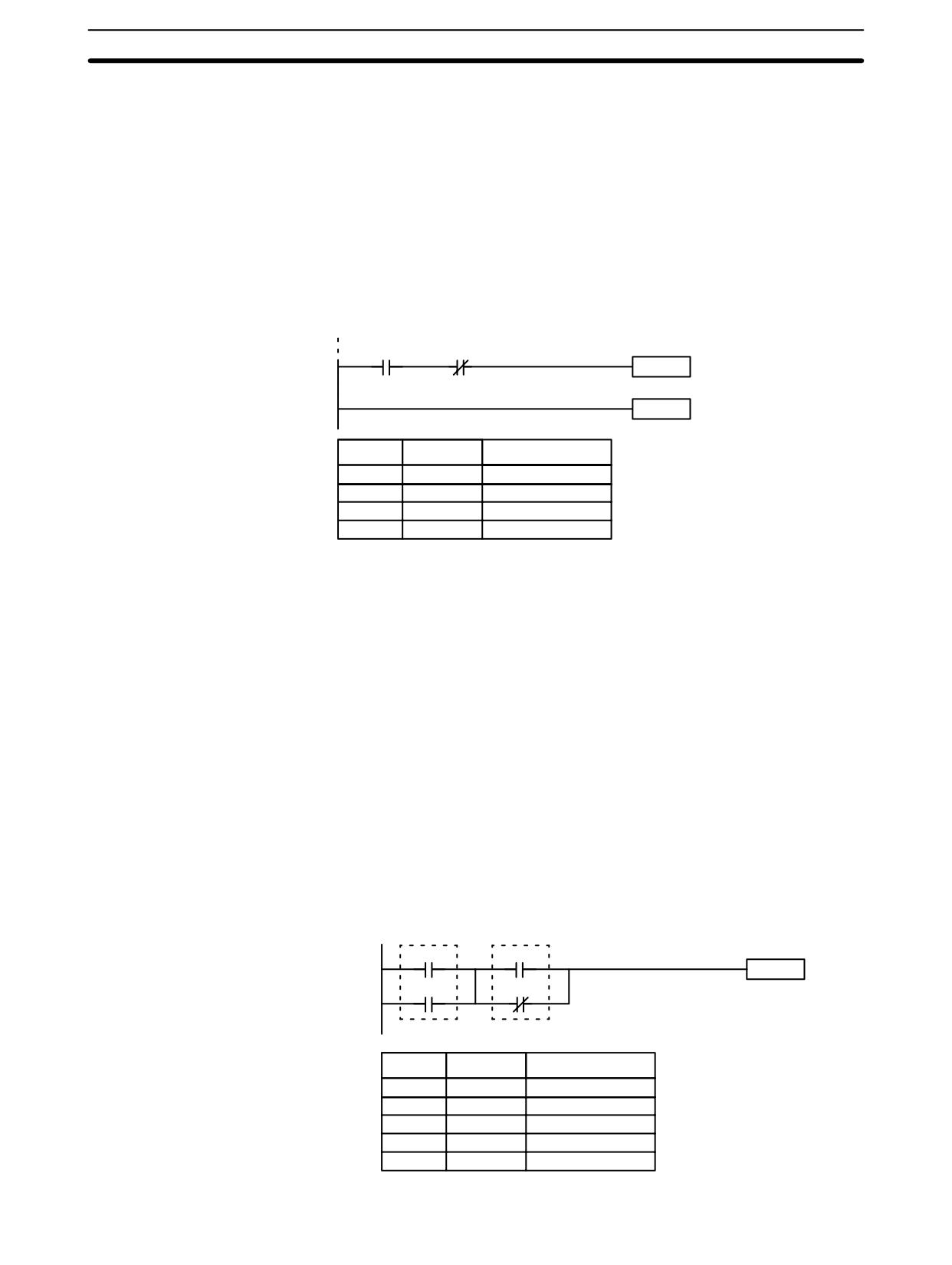
Basic Ladder Diagrams
Section
6-3
6-3-5
The END Instruction
The last instruction required to complete a simple program is the END instruc-
tion. When the CPU Unit scans the program, it executes all instructions up to the
first END instruction before returning to the beginning of the program and begin-
ning execution again. Although an END instruction can be placed at any point in
a program, which is sometimes done when debugging, no instructions past the
first END instruction will be executed until it is removed. The number following
the END instruction in the mnemonic code is its function code, which is used
when inputted most instruction into the PC. These are described later. The END
instruction requires no operands and no conditions can be placed on the same
instruction line with it.
00000
00001
Instruction
Program execution
END(01)
ends here.
Address
Instruction
Operands
00500
LD
00000
00501
AND NOT
00001
00502
Instruction
00503
END(01)
---
If there is no END instruction anywhere in the program, the program will not be
executed at all.
Now you have all of the instructions required to write simple input-output pro-
grams. Before we finish with ladder diagram basic and go onto inputting the pro-
gram into the PC, let’s look at logic block instruction (AND LOAD and OR LOAD),
which are sometimes necessary even with simple diagrams.
6-3-6
Logic Block Instructions
Logic block instructions do not correspond to specific conditions on the ladder
diagram; rather, they describe relationships between logic blocks. The AND
LOAD instruction logically ANDs the execution conditions produced by two logic
blocks. The OR LOAD instruction logically ORs the execution conditions pro-
duced by two logic blocks.
AND LOAD
Although simple in appearance, the diagram below requires an AND LOAD
instruction.
00000
00002
Instruction
00001
00003
Address
Instruction
Operands
00000
LD
00000
00001
OR
00001
00002
LD
00002
00003
OR NOT
00003
00004
AND LD
---
337
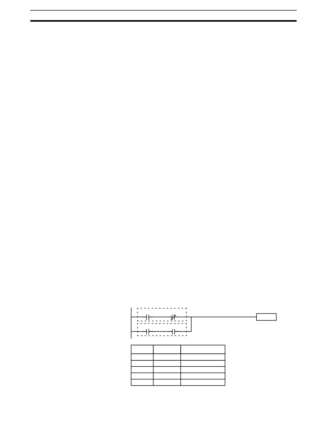
Basic Ladder Diagrams
Section
6-3
The two logic blocks are indicated by dotted lines. Studying this example shows
that an ON execution condition will be produced when: either of the conditions in
the left logic block is ON (i.e., when either IR 00000 or IR 00001 is ON), and
when either of the conditions in the right logic block is ON (i.e., when either IR
00002 is ON or IR 00003 is OFF).
The above ladder diagram cannot, however, be converted to mnemonic code
using AND and OR instructions alone. If an AND between IR 00002 and the re-
sults of an OR between IR 00000 and IR 00001 is attempted, the OR NOT be-
tween IR 00002 and IR 00003 is lost and the OR NOT ends up being an OR NOT
between just IR 00003 and the result of an AND between IR 00002 and the first
OR. What we need is a way to do the OR (NOT)’s independently and then com-
bine the results.
To do this, we can use the LOAD or LOAD NOT instruction in the middle of an
instruction line. When LOAD or LOAD NOT is executed in this way, the current
execution condition is saved in special buffers and the logic process is begun
over. To combine the results of the current execution condition with that of a pre-
vious “unused” execution condition, an AND LOAD or an OR LOAD instruction is
used. Here “LOAD” refers to loading the last unused execution condition. An un-
used execution condition is produced by using the LOAD or LOAD NOT instruc-
tion for any but the first condition on an instruction line.
Analyzing the above ladder diagram in terms of mnemonic instructions, the
condition for IR 00000 is a LOAD instruction and the condition below it is an OR
instruction between the status of IR 00000 and that of IR 00001. The condition at
IR 00002 is another LOAD instruction and the condition below is an OR NOT
instruction, i.e., an OR between the status of IR 00002 and the inverse of the
status of IR 00003. To arrive at the execution condition for the instruction at the
right, the logical AND of the execution conditions resulting from these two blocks
would have to be taken. AND LOAD does this. The mnemonic code for the lad-
der diagram is shown below. The AND LOAD instruction requires no operands of
its own, because it operates on previously determined execution conditions.
Here too, dashes are used to indicate that no operands needs designated or in-
put.
OR LOAD
The following diagram requires an OR LOAD instruction between the top logic
block and the bottom logic block. An ON execution condition would be produced
for the instruction at the right either when IR 00000 is ON and IR 00001 is OFF or
when IR 00002 and IR 00003 are both ON. The operation of and mnemonic code
for the OR LOAD instruction is exactly the same as those for a AND LOAD
instruction except that the current execution condition is ORed with the last un-
used execution condition.
00000
00001
Instruction
00002
00003
Address
Instruction
Operands
00000
LD
00000
00001
AND NOT
00001
00002
LD
00002
00003
AND
00003
00004
OR LD
---
Naturally, some diagrams will require both AND LOAD and OR LOAD instruc-
tions.
338
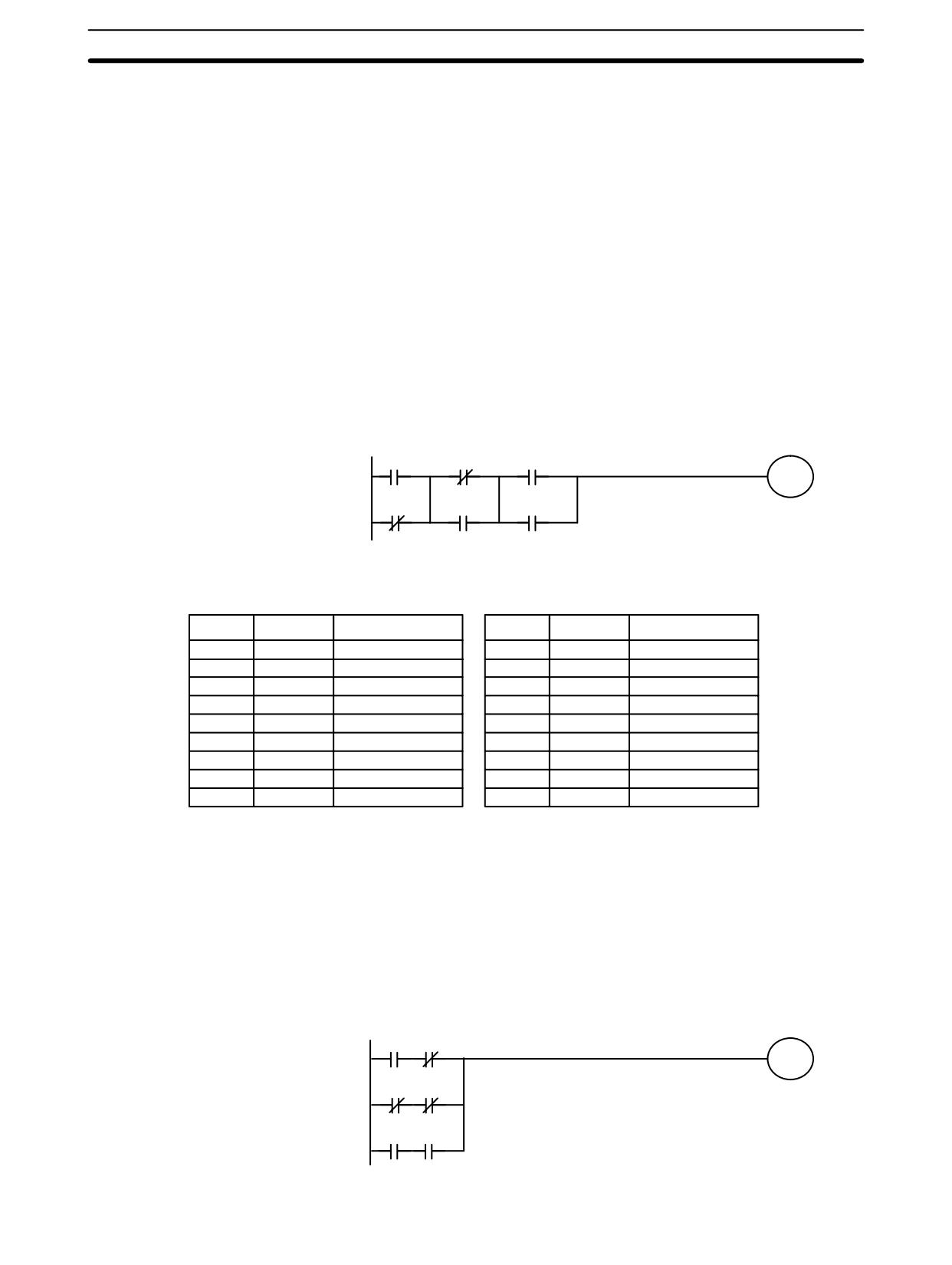
Basic Ladder Diagrams
Section
6-3
To code diagrams with logic block instructions in series, the diagram must be
Logic Block Instructions in
Series
divided into logic blocks. Each block is coded using a LOAD instruction to code
the first condition, and then AND LOAD or OR LOAD is used to logically combine
the blocks. With both AND LOAD and OR LOAD there are two ways to achieve
this. One is to code the logic block instruction after the first two blocks and then
after each additional block. The other is to code all of the blocks to be combined,
starting each block with LOAD or LOAD NOT, and then to code the logic block
instructions which combine them. In this case, the instructions for the last pair of
blocks should be combined first, and then each preceding block should be com-
bined, working progressively back to the first block. Although either of these
methods will produce exactly the same result, the second method, that of coding
all logic block instructions together, can be used only if eight or fewer blocks are
being combined, i.e., if seven or fewer logic block instructions are required.
The following diagram requires AND LOAD to be converted to mnemonic code
because three pairs of parallel conditions lie in series. The two means of coding
the programs are also shown.
00000
00002
00004
20000
00001
00003
00005
Address
Instruction
Operands
Address
Instruction
Operands
00000
LD
00000
00000
LD
00000
00001
OR NOT
00001
00001
OR NOT
00001
00002
LD NOT
00002
00002
LD NOT
00002
00003
OR
00003
00003
OR
00003
00004
AND LD
-
00004
LD
00004
00005
LD
00004
00005
OR
00005
00006
OR
00005
00006
AND LD
-
00007
AND LD
-
00007
AND LD
-
00008
OUT
20000
00008
OUT
20000
Again, with the method on the right, a maximum of eight blocks can be com-
bined. There is no limit to the number of blocks that can be combined with the
first method.
The following diagram requires OR LOAD instructions to be converted to mne-
monic code because three pairs of conditions in series lie in parallel to each oth-
er.
00000
00001
20001
00002
00003
00004
00005
339
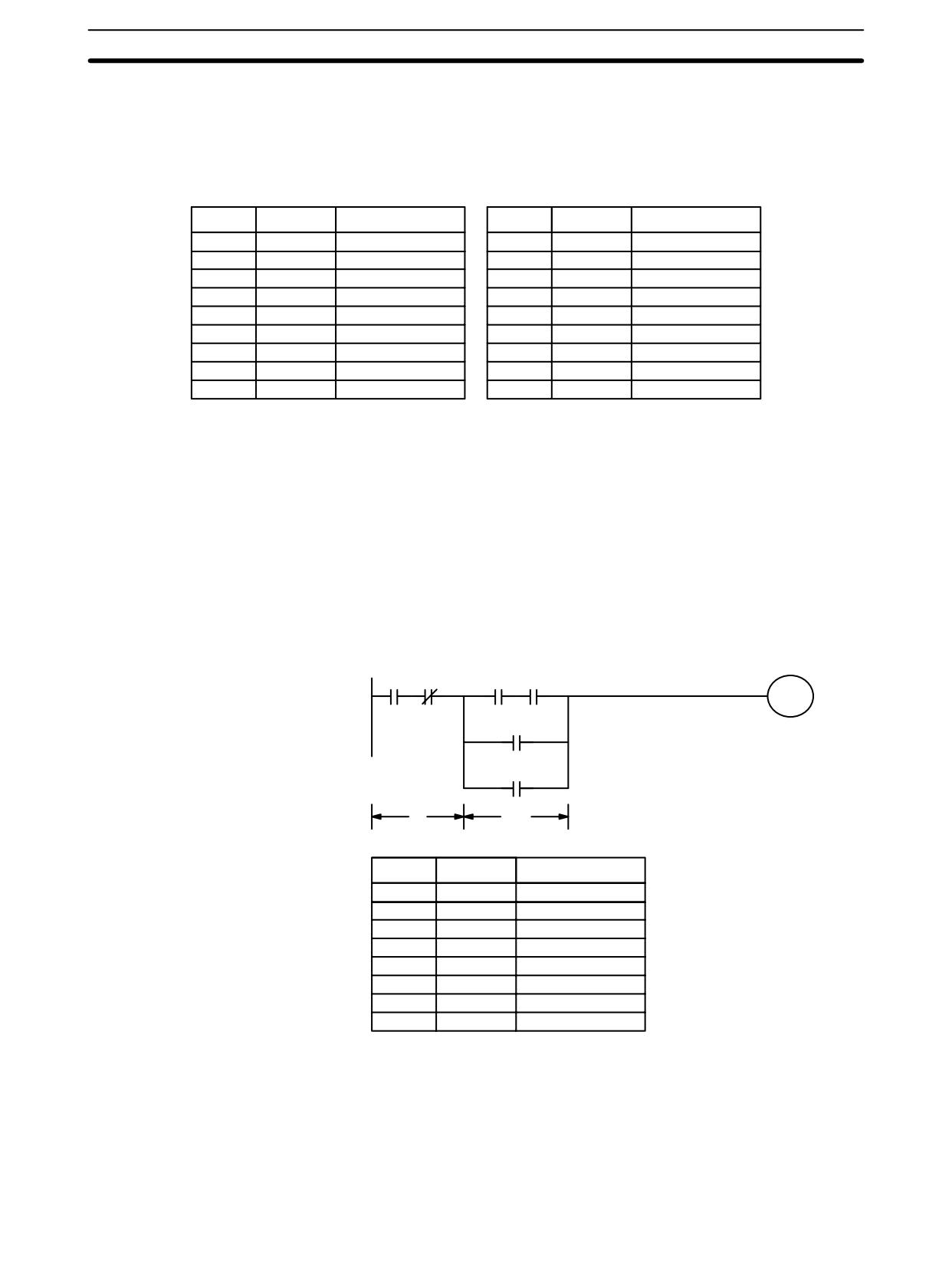
Basic Ladder Diagrams
Section
6-3
The first of each pair of conditions is converted to LOAD with the assigned bit
operand and then ANDed with the other condition. The first two blocks can be
coded first, followed by OR LOAD, the last block, and another OR LOAD, or the
three blocks can be coded first followed by two OR LOADs. The mnemonic code
for both methods is shown below.
Address
Instruction
Operands
Address
Instruction
Operands
00000
LD
00000
00000
LD
00000
00001
AND NOT
00001
00001
AND NOT
00001
00002
LD NOT
00002
00002
LD NOT
00002
00003
AND NOT
00003
00003
AND NOT
00003
00004
OR LD
-
00004
LD
00004
00005
LD
00004
00005
AND
00005
00006
AND
00005
00006
OR LD
-
00007
OR LD
-
00007
OR LD
-
00008
OUT
20001
00008
OUT
20001
Again, with the method on the right, a maximum of eight blocks can be com-
bined. There is no limit to the number of blocks that can be combined with the
first method.
Both of the coding methods described above can also be used when using AND
Combining AND LOAD and
OR LOAD
LOAD and OR LOAD, as long as the number of blocks being combined does not
exceed eight.
The following diagram contains only two logic blocks as shown. It is not neces-
sary to further separate block b components, because it can coded directly using
only AND and OR.
00000
00001
00002
00003
20001
00201
00004
Block
Block
a
b
Address
Instruction
Operands
00000
LD
00000
00001
AND NOT
00001
00002
LD
00002
00003
AND
00003
00004
OR
00201
00005
OR
00004
00006
AND LD
-
00007
OUT
20001
Although the following diagram is similar to the one above, block b in the diagram
below cannot be coded without separating it into two blocks combined with OR
LOAD. In this example, the three blocks have been coded first and then OR
LOAD has been used to combine the last two blocks followed by AND LOAD to
combine the execution condition produced by the OR LOAD with the execution
condition of block a.
340
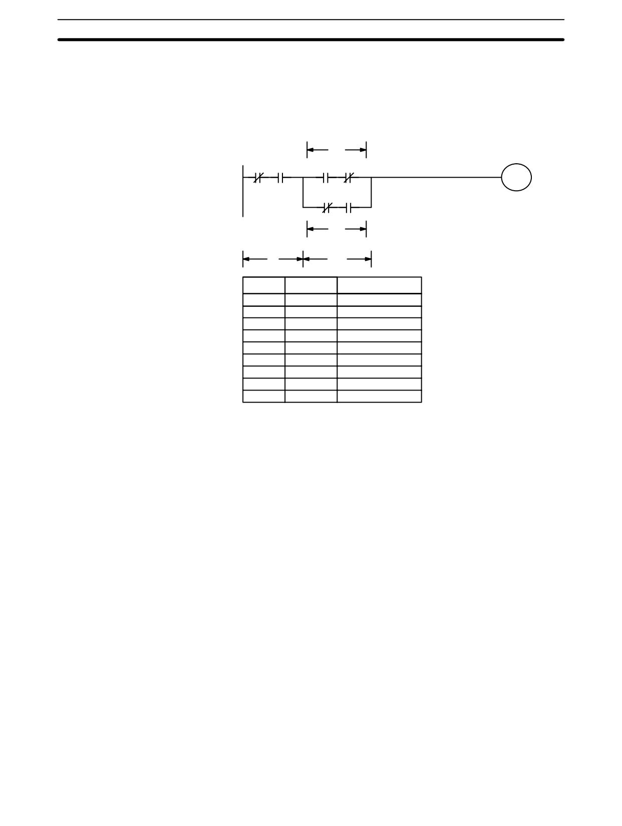
Basic Ladder Diagrams
Section
6-3
When coding the logic block instructions together at the end of the logic blocks
they are combining, they must, as shown below, be coded in reverse order, i.e.,
the logic block instruction for the last two blocks is coded first, followed by the
one to combine the execution condition resulting from the first logic block
instruction and the execution condition of the logic block third from the end, and
on back to the first logic block that is being combined.
Block
b1
00000
00001
00002
00003
20002
00004
00202
Block
b2
Block
Block
a
b
Address
Instruction
Operands
00000
LD NOT
00000
00001
AND
00001
00002
LD
00002
00003
AND NOT
00003
00004
LD NOT
00004
00005
AND
00202
00006
OR LD
-
00007
AND LD
-
00008
OUT
20002
When determining what logic block instructions will be required to code a dia-
Complicated Diagrams
gram, it is sometimes necessary to break the diagram into large blocks and then
continue breaking the large blocks down until logic blocks that can be coded
without logic block instructions have been formed. These blocks are then coded,
combining the small blocks first, and then combining the larger blocks. Either
AND LOAD or OR LOAD is used to combine the blocks, i.e., AND LOAD or OR
LOAD always combines the last two execution conditions that existed, regard-
less of whether the execution conditions resulted from a single condition, from
logic blocks, or from previous logic block instructions.
When working with complicated diagrams, blocks will ultimately be coded start-
ing at the top left and moving down before moving across. This will generally
mean that, when there might be a choice, OR LOAD will be coded before AND
LOAD.
341
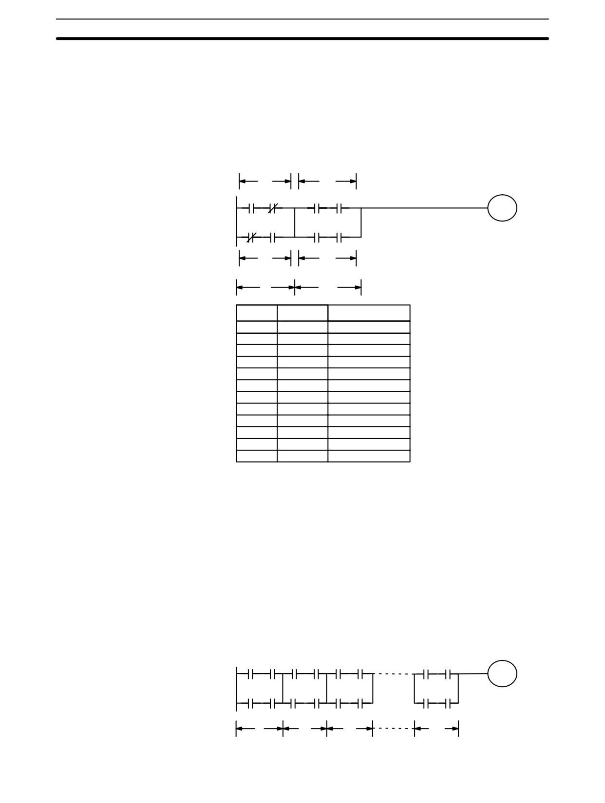
Basic Ladder Diagrams
Section
6-3
The following diagram must be broken down into two blocks and each of these
then broken into two blocks before it can be coded. As shown below, blocks a
and b require an AND LOAD. Before AND LOAD can be used, however, OR
LOAD must be used to combine the top and bottom blocks on both sides, i.e., to
combine a1 and a2; b1 and b2.
Block
Block
a1
b1
00000
00001
00004
00005
20003
00002
00003
00006
00007
Block
Block
a2
b2
Block
Block
a
b
Address
Instruction
Operands
00000
LD
00000
00001
AND NOT
00001
00002
LD NOT
00002
00003
AND
00003
00004
OR LD
-
Blocks a1 and a2
00005
LD
00004
00006
AND
00005
00007
LD
00006
00008
AND
00007
00009
OR LD
-
Blocks b1 and b2
00010
AND LD
-
Blocks a and b
00011
OUT
20003
The following type of diagram can be coded easily if each block is coded in order:
first top to bottom and then left to right. In the following diagram, blocks a and b
would be combined using AND LOAD as shown above, and then block c would
be coded and a second AND LOAD would be used to combined it with the execu-
tion condition from the first AND LOAD. Then block d would be coded, a third
AND LOAD would be used to combine the execution condition from block d with
the execution condition from the second AND LOAD, and so on through to block
n.
20000
Block
Block
Block
Block
a
b
c
n
342
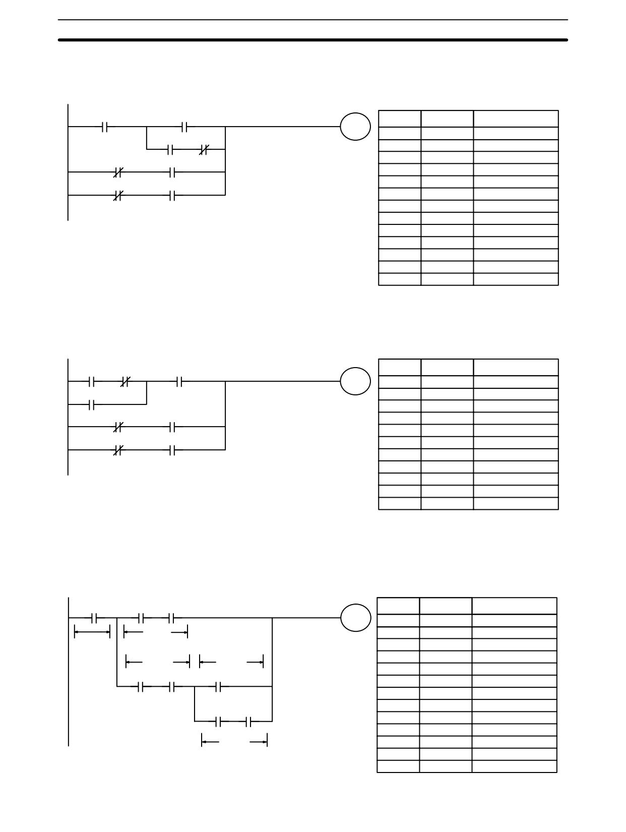
Basic Ladder Diagrams
Section
6-3
The following diagram requires an OR LOAD followed by an AND LOAD to code
the top of the three blocks, and then two more OR LOADs to complete the mne-
monic code.
00000
00001
Address
Instruction
Operands
LR 0000
00000
LD
00000
00002
00003
00001
LD
00001
00002
LD
00002
00004
00005
00003
AND NOT
00003
00004
OR LD
--
00006
00007
00005
AND LD
--
00006
LD NOT
00004
00007
AND
00005
00008
OR LD
--
00009
LD NOT
00006
00010
AND
00007
00011
OR LD
--
00012
OUT
LR
0000
Although the program will execute as written, this diagram could be drawn as
shown below to eliminate the need for the first OR LOAD and the AND LOAD,
simplifying the program and saving memory space.
Address
Instruction
Operands
00002
00003
00000
LR 0000
00000
LD
00002
00001
00001
AND NOT
00003
00002
OR
00001
00004
00005
00003
AND
00000
00004
LD NOT
00004
00006
00007
00005
AND
00005
00006
OR LD
--
00007
LD NOT
00006
00008
AND
00007
00009
OR LD
--
00010
OUT
LR
0000
The following diagram requires five blocks, which here are coded in order before
using OR LOAD and AND LOAD to combine them starting from the last two
blocks and working backward. The OR LOAD at program address 00008 com-
bines blocks d and e, the following AND LOAD combines the resulting execution
condition with that of block c, etc.
00000
00001
00002
Address
Instruction
Operands
LR 0000
00000
LD
00000
Block b
00001
LD
00001
Block a
00002
AND
00002
00003
LD
00003
Block c
Block d
00004
AND
00004
00003
00004
00005
00005
LD
00005
00006
LD
00006
00007
AND
00007
00006
00007
00008
OR LD
--
Blocks d and e
00009
AND LD
--
Block e
Block c with result of above
00010
OR LD
--
Block b with result of above
00011
AND LD
--
Block a with result of above
00012
OUT
LR
0000
343
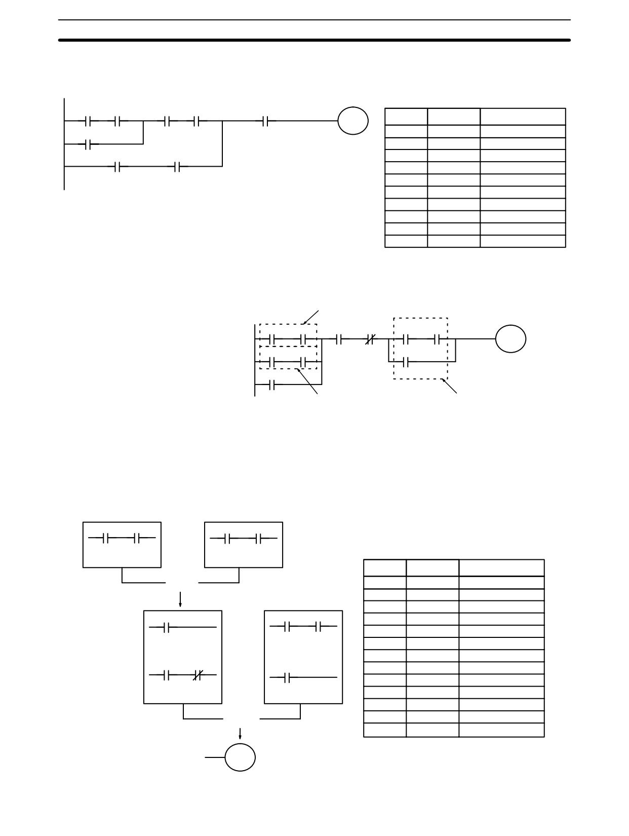
Basic Ladder Diagrams
Section
6-3
Again, this diagram can be redrawn as follows to simplify program structure and
coding and to save memory space.
00006
00007
00003
00004
00000
Address
Instruction
Operands
LR 0000
00000
LD
00006
00005
00001
AND
00007
00001
00002
00002
OR
00005
00003
AND
00003
00004
AND
00004
00005
LD
00001
00006
AND
00002
00007
OR LD
--
00008
AND
00000
00009
OUT
LR
0000
The next and final example may at first appear very complicated but can be
coded using only two logic block instructions. The diagram appears as follows:
Block a
00000
00001
00002
00003
00004
00005
20000
01000
01001
00006
20000
Block b
Block c
The first logic block instruction is used to combine the execution conditions re-
sulting from blocks a and b, and the second one is to combine the execution
condition of block c with the execution condition resulting from the normally
closed condition assigned IR 00003. The rest of the diagram can be coded with
OR, AND, and AND NOT instructions. The logical flow for this and the resulting
code are shown below.
Block a
Block b
00000
00001
01000
01001
LD
00000
LD
01000
AND
00001
AND
01001
Address
Instruction
Operands
OR LD
00000
LD
00000
00001
AND
00001
Block c
00002
LD
01000
20000
00004
00005
00003
AND
01001
00004
OR LD
--
OR
20000
LD
00004
AND
00005
00005
OR
20000
00006
AND
00002
00002
00003
00006
00007
AND NOT
00003
00008
LD
00004
AND
00002
OR
00006
00009
AND
00005
AND NOT 00003
00010
OR
00006
00011
AND LD
--
AND LD
00012
OUT
20000
20000
344
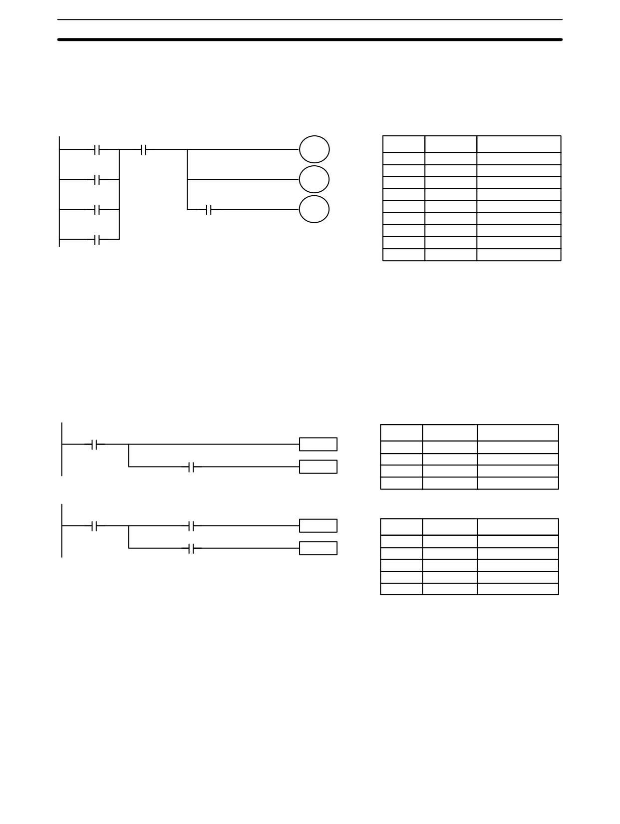
Basic Ladder Diagrams
Section
6-3
6-3-7
Coding Multiple Right-hand Instructions
If there is more than one right-hand instruction executed with the same execu-
tion condition, they are coded consecutively following the last condition on the
instruction line. In the following example, the last instruction line contains one
more condition that corresponds to an AND with IR 00004.
00000
00003
Address
Instruction
Operands
HR 0001
00000
LD
00000
00001
00001
OR
00001
20000
00002
OR
00002
00003
OR
HR
0000
00002
00004
20001
00004
AND
00003
00005
OUT
HR
0001
HR 0000
00006
OUT
20000
00007
AND
00004
00008
OUT
20001
6-3-8
Branching Instruction Lines
When an instruction line branches into two or more lines, it is sometimes neces-
sary to use either interlocks or TR bits to maintain the execution condition that
existed at a branching point. This is because instruction lines are executed
across to a right-hand instruction before returning to the branching point to
execute instructions one a branch line. If a condition exists on any of the instruc-
tion lines after the branching point, the execution condition could change during
this time making proper execution impossible. The following diagrams illustrate
this. In both diagrams, instruction 1 is executed before returning to the branching
point and moving on to the branch line leading to instruction 2.
Branching
00000
point
Address
Instruction
Operands
Instruction 1
00000
LD
00000
00002
00001
Instruction 1
Instruction 2
00002
AND
00002
00003
Instruction 2
Diagram A: Correct Operation
Branching
00000
point
00001
Instruction 1
Address
Instruction
Operands
00002
00000
LD
00000
Instruction 2
00001
AND
00001
Diagram B: Incorrect Operation
00002
Instruction 1
00003
AND
00002
00004
Instruction 2
If, as shown in diagram A, the execution condition that existed at the branching
point cannot be changed before returning to the branch line (instructions at the
far right do not change the execution condition), then the branch line will be
executed correctly and no special programming measure is required.
If, as shown in diagram B, a condition exists between the branching point and the
last instruction on the top instruction line, the execution condition at the branch-
ing point and the execution condition after completing the top instruction line will
sometimes be different, making it impossible to ensure correct execution of the
branch line.
There are two means of programming branching programs to preserve the
execution condition. One is to use TR bits; the other, to use interlocks
(IL(02)/IL(03)).
345
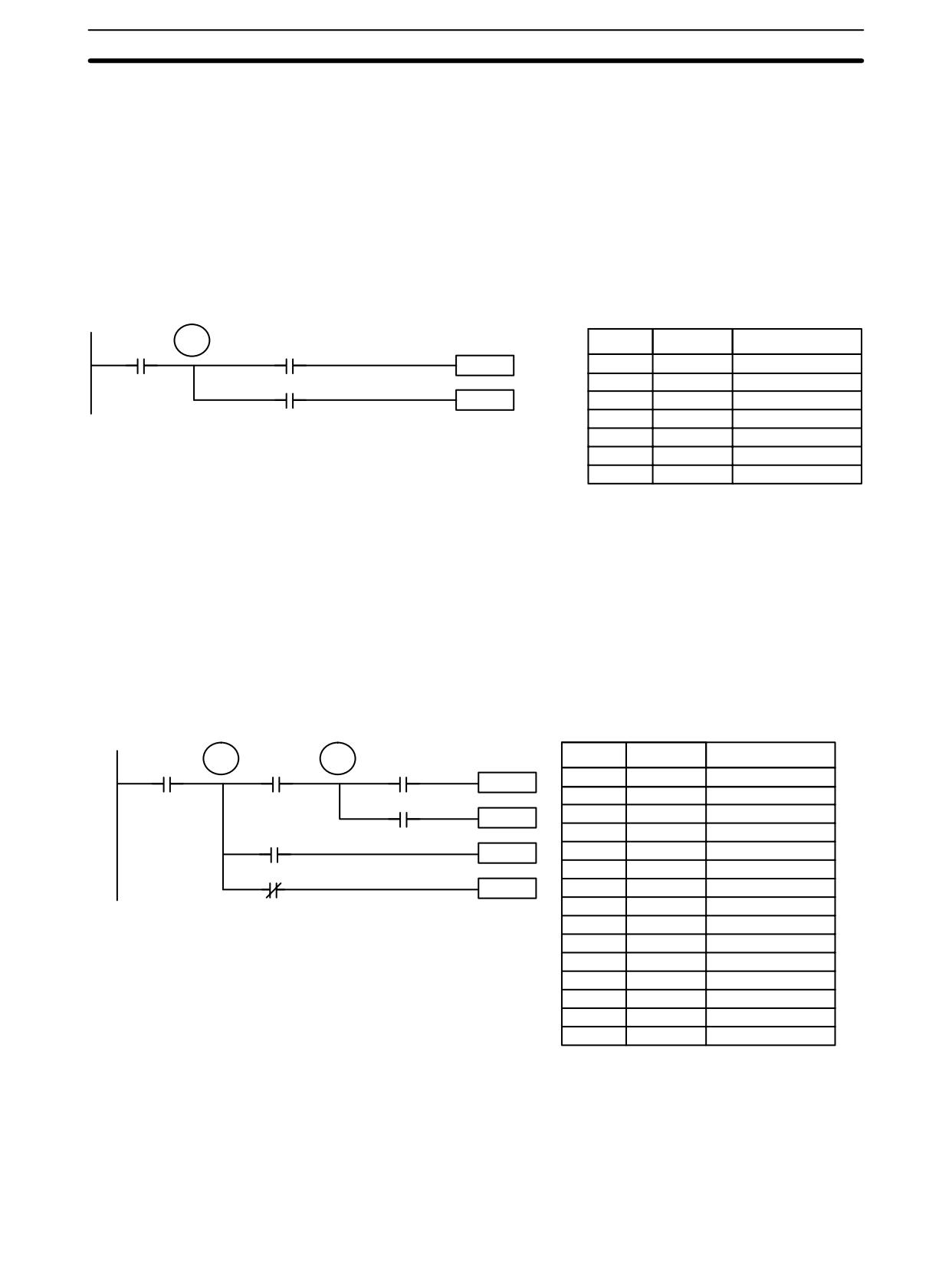
Basic Ladder Diagrams
Section
6-3
The TR area provides eight bits, TR 0 through TR 7, that can be used to tempo-
TR Bits
rarily preserve execution conditions. If a TR bit is placed at a branching point, the
current execution condition will be stored at the designated TR bit. When return-
ing to the branching point, the TR bit restores the execution status that was
saved when the branching point was first reached in program execution.
The previous diagram B can be written as shown below to ensure correct execu-
tion. In mnemonic code, the execution condition is stored at the branching point
using the TR bit as the operand of the OUTPUT instruction. This execution
condition is then restored after executing the right-hand instruction by using the
same TR bit as the operand of a LOAD instruction
TR 0
Address
Instruction
Operands
00000
00001
Instruction 1
00000
LD
00000
00002
00001
OUT
TR
0
Instruction 2
00002
AND
00001
00003
Instruction 1
Diagram B: Corrected Using a TR bit
00004
LD
TR
0
00005
AND
00002
00006
Instruction 2
In terms of actual instructions the above diagram would be as follows: The status
of IR 00000 is loaded (a LOAD instruction) to establish the initial execution
condition. This execution condition is then output using an OUTPUT instruction
to TR 0 to store the execution condition at the branching point. The execution
condition is then ANDed with the status of IR 00001 and instruction 1 is executed
accordingly. The execution condition that was stored at the branching point is
then re-loaded (a LOAD instruction with TR 0 as the operand), this is ANDed with
the status of IR 00002, and instruction 2 is executed accordingly.
The following example shows an application using two TR bits.
TR 0
TR 1
Address
Instruction
Operands
00000
00001
00002
00000
LD
00000
Instruction 1
00001
OUT
TR
0
00003
Instruction 2
00002
AND
00001
00003
OUT
TR
1
00004
Instruction 3
00004
AND
00002
00005
Instruction 1
00005
Instruction 4
00006
LD
TR
1
00007
AND
00003
00008
Instruction 2
00009
LD
TR
0
00010
AND
00004
00011
Instruction 3
00012
LD
TR
0
00013
AND NOT
00005
00014
Instruction 4
In this example, TR 0 and TR 1 are used to store the execution conditions at the
branching points. After executing instruction 1, the execution condition stored in
TR 1 is loaded for an AND with the status IR 00003. The execution condition
stored in TR 0 is loaded twice, the first time for an AND with the status of IR
00004 and the second time for an AND with the inverse of the status of IR 00005.
346
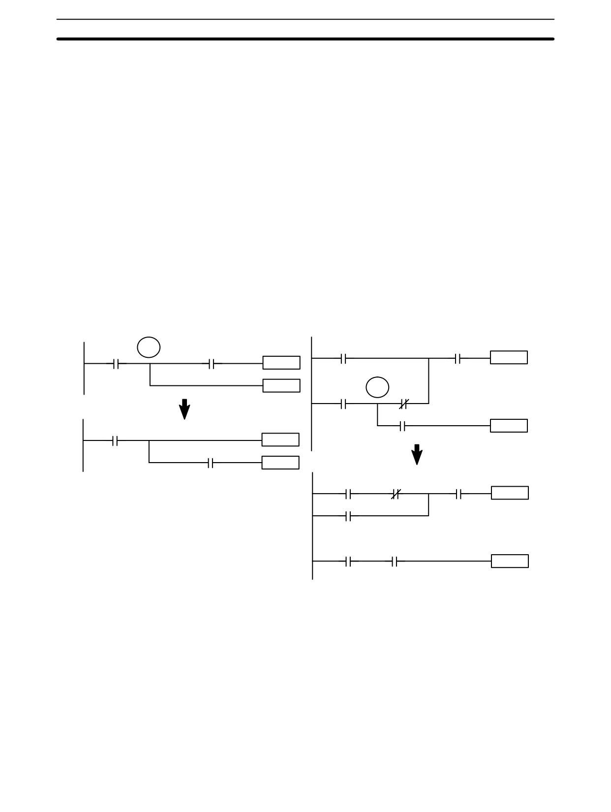
Basic Ladder Diagrams
Section
6-3
TR bits can be used as many times as required as long as the same TR bit is not
used more than once in the same instruction block. Here, a new instruction block
is begun each time execution returns to the bus bar. If, in a single instruction
block, it is necessary to have more than eight branching points that require the
execution condition be saved, interlocks (which are described next) must be
used.
When drawing a ladder diagram, be careful not to use TR bits unless necessary.
Often the number of instructions required for a program can be reduced and
ease of understanding a program increased by redrawing a diagram that would
otherwise required TR bits. In both of the following pairs of diagrams, the bottom
versions require fewer instructions and do not require TR bits. In the first exam-
ple, this is achieved by reorganizing the parts of the instruction block: the bottom
one, by separating the second OUTPUT instruction and using another LOAD
instruction to create the proper execution condition for it.
Note Although simplifying programs is always a concern, the order of execution of
instructions is sometimes important. For example, a MOVE instruction may be
required before the execution of a BINARY ADD instruction to place the proper
data in the required operand word. Be sure that you have considered execution
order before reorganizing a program to simplify it.
TR 0
00000
00003
00000
00001
Instruction 1
Instruction 1
Instruction 2
TR 0
00001
00002
00004
Instruction 2
00000
Instruction 2
00001
Instruction 1
00001
00002
00003
Instruction 1
00000
00001
00004
Instruction 2
Note TR bits are must be input by the user only when programming using mnemonic
code. They are not necessary when inputting ladder diagrams directly because
they are processed for you automatically. The above limitations on the number
of branching points requiring TR bits, and considerations on methods to reduce
the number of programming instructions, still hold.
The problem of storing execution conditions at branching points can also be
Interlocks
handled by using the INTERLOCK (IL(02)) and INTERLOCK CLEAR (ILC(03))
instructions to eliminate the branching point completely while allowing a specific
execution condition to control a group of instructions. The INTERLOCK and IN-
TERLOCK CLEAR instructions are always used together.
347
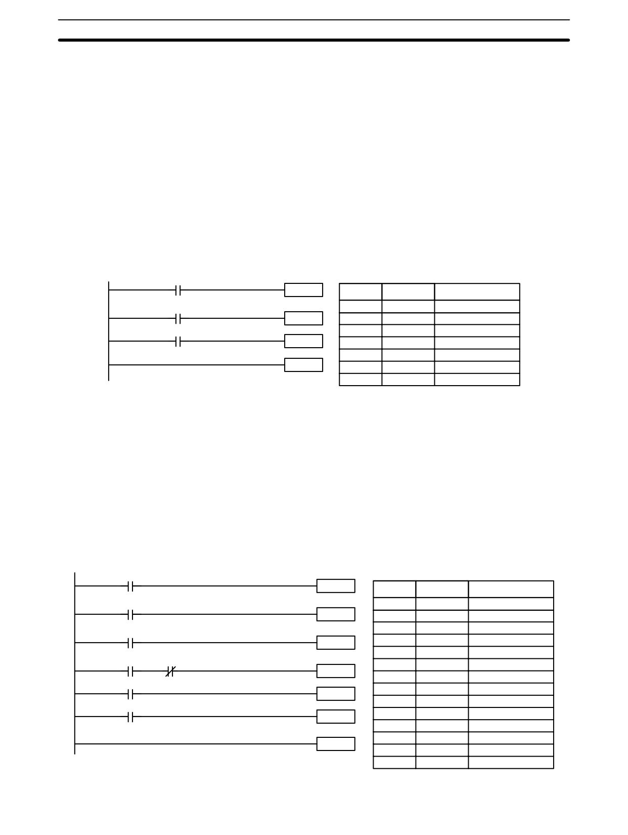
Basic Ladder Diagrams
Section
6-3
When an INTERLOCK instruction is placed before a section of a ladder pro-
gram, the execution condition for the INTERLOCK instruction will control the
execution of all instruction up to the next INTERLOCK CLEAR instruction. If the
execution condition for the INTERLOCK instruction is OFF, all right-hand
instructions through the next INTERLOCK CLEAR instruction will be executed
with OFF execution conditions to reset the entire section of the ladder diagram.
The effect that this has on particular instructions is described in 7-11 INTER-
LOCK and INTERLOCK CLEAR - IL(02) and ILC(03).
Diagram B can also be corrected with an interlock. Here, the conditions leading
up to the branching point are placed on an instruction line for the INTERLOCK
instruction, all of lines leading from the branching point are written as separate
instruction lines, and another instruction line is added for the INTERLOCK
CLEAR instruction. No conditions are allowed on the instruction line for INTER-
LOCK CLEAR. Note that neither INTERLOCK nor INTERLOCK CLEAR re-
quires an operand.
00000
IL(02)
Address
Instruction
Operands
00001
00000
LD
00000
Instruction 1
00001
IL(02)
---
00002
00002
LD
00001
Instruction 2
00003
Instruction 1
00004
LD
00002
ILC(03)
00005
Instruction 2
00006
ILC(03)
---
If IR 00000 is ON in the revised version of diagram B, above, the status of IR
00001 and that of IR 00002 would determine the execution conditions for
instructions 1 and 2, respectively. Because IR 00000 is ON, this would produce
the same results as ANDing the status of each of these bits. If IR 00000 is OFF,
the INTERLOCK instruction would produce an OFF execution condition for
instructions 1 and 2 and then execution would continue with the instruction line
following the INTERLOCK CLEAR instruction.
As shown in the following diagram, more than one INTERLOCK instruction can
be used within one instruction block; each is effective through the next INTER-
LOCK CLEAR instruction.
00000
IL(02)
Address
Instruction
Operands
00001
00000
LD
00000
Instruction 1
00001
IL(02)
---
00002
LD
00001
00002
00003
Instruction 1
IL(02)
00004
LD
00002
00003
00004
00005
IL(02)
---
Instruction 2
00006
LD
00003
00005
00007
AND NOT
00004
Instruction 3
00008
Instruction 2
00006
Instruction 4
00009
LD
00005
00010
Instruction 3
00011
LD
00006
ILC(03)
00012
Instruction 4
00013
ILC(03)
---
348

Basic Ladder Diagrams
Section
6-3
If IR 00000 in the above diagram is OFF (i.e., if the execution condition for the
first INTERLOCK instruction is OFF), instructions 1 through 4 would be
executed with OFF execution conditions and execution would move to the
instruction following the INTERLOCK CLEAR instruction. If IR 00000 is ON, the
status of IR 00001 would be loaded as the execution condition for instruction 1
and then the status of IR 00002 would be loaded to form the execution condition
for the second INTERLOCK instruction. If IR 00002 is OFF, instructions 2
through 4 will be executed with OFF execution conditions. If IR 00002 is ON, IR
00003, IR 00005, and IR 00006 will determine the first execution condition in
new instruction lines.
6-3-9
Jumps
A specific section of a program can be skipped according to a designated execu-
tion condition. Although this is similar to what happens when the execution
condition for an INTERLOCK instruction is OFF, with jumps, the operands for all
instructions maintain status. Jumps can therefore be used to control devices
that require a sustained output, e.g., pneumatics and hydraulics, whereas inter-
locks can be used to control devices that do not required a sustained output,
e.g., electronic instruments.
Jumps are created using the JUMP (JMP(04)) and JUMP END (JME(05))
instructions. If the execution condition for a JUMP instruction is ON, the program
is executed normally as if the jump did not exist. If the execution condition for the
JUMP instruction is OFF, program execution moves immediately to a JUMP
END instruction without changing the status of anything between the JUMP and
JUMP END instruction.
All JUMP and JUMP END instructions are assigned jump numbers ranging be-
tween 00 and 99. There are two types of jumps. The jump number used deter-
mines the type of jump.
A jump can be defined using jump numbers 01 through 99 only once, i.e., each of
these numbers can be used once in a JUMP instruction and once in a JUMP
END instruction. When a JUMP instruction assigned one of these numbers is
executed, execution moves immediately to the JUMP END instruction that has
the same number as if all of the instruction between them did not exist. Diagram
B from the TR bit and interlock example could be redrawn as shown below using
a jump. Although 01 has been used as the jump number, any number between
01 and 99 could be used as long as it has not already been used in a different part
of the program. JUMP and JUMP END require no other operand and JUMP END
never has conditions on the instruction line leading to it.
00000
JMP(04) 01
Address
Instruction
Operands
00001
00000
LD
00000
Instruction 1
00001
JMP(04)
01
00002
00002
LD
00001
Instruction 2
00003
Instruction 1
00004
LD
00002
JME(05) 01
00005
Instruction 2
00006
JME(05)
01
Diagram B: Corrected with a Jump
This version of diagram B would have a shorter execution time when IR 00000
was OFF than any of the other versions.
349
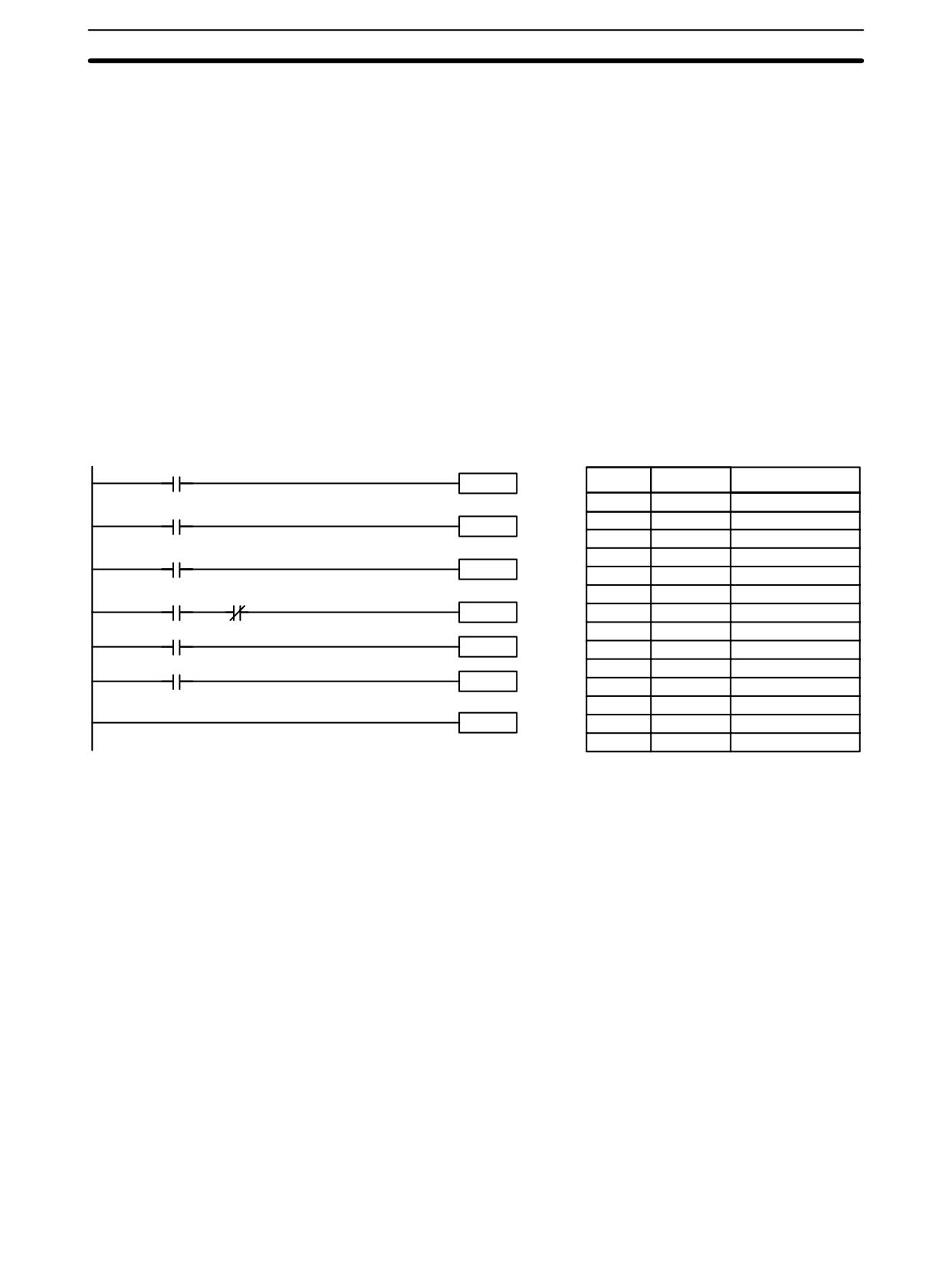
Controlling Bit Status
Section
6-4
The other type of jump is created with a jump number of 00. As many jumps as
desired can be created using jump number 00 and JUMP instructions using 00
can be used consecutively without a JUMP END using 00 between them. It is
even possible for all JUMP 00 instructions to move program execution to the
same JUMP END 00, i.e., only one JUMP END 00 instruction is required for all
JUMP 00 instruction in the program. When 00 is used as the jump number for a
JUMP instruction, program execution moves to the instruction following the next
JUMP END instruction with a jump number of 00. Although, as in all jumps, no
status is changed and no instructions are executed between the JUMP 00 and
JUMP END 00 instructions, the program must search for the next JUMP END 00
instruction, producing a slightly longer execution time.
Execution of programs containing multiple JUMP 00 instructions for one JUMP
END 00 instruction is similar to that of interlocked sections. The following dia-
gram is the same as that used for the interlock example above, except redrawn
with jumps. The execution of this diagram would differ from that of the diagram
described above (e.g., in the previous diagram interlocks would reset certain
parts of the interlocked section, however, jumps do not affect the status of any bit
between the JUMP and JUMP END instructions).
00000
JMP(04) 00
Address
Instruction
Operands
00000
LD
00000
00001
00001
JMP(04)
00
Instruction 1
00002
LD
00001
00002
00003
Instruction 1
JMP(04) 00
00004
LD
00002
00003
00004
00005
JMP(04)
00
Instruction 2
00006
LD
00003
00005
00007
AND NOT
00004
Instruction 3
00008
Instruction 2
00006
00009
LD
00005
Instruction 4
00010
Instruction 3
00011
LD
00006
JME(05) 00
00012
Instruction 4
00013
JME(05)
00
6-4
Controlling Bit Status
There are seven basic instructions that can be used generally to control individu-
al bit status. These are the OUTPUT, OUTPUT NOT, SET, RESET, DIFFER-
ENTIATE UP, DIFFERENTIATE DOWN, and KEEP instructions. All of these
instructions appear as the last instruction in an instruction line and take a bit ad-
dress for an operand. Although details are provided in 7-8 Bit Control Instruc-
tions, these instructions (except for OUTPUT and OUTPUT NOT, which have
already been introduced) are described here because of their importance in
most programs. Although these instructions are used to turn ON and OFF output
bits in the IR area (i.e., to send or stop output signals to external devices), they
are also used to control the status of other bits in the IR area or in other data
areas.
6-4-1
SET and RESET
The SET and RESET instructions are very similar to the OUTPUT and OUTPUT
NOT instructions except that they only change the status of their operand bits for
ON execution conditions. Neither instructions will affect the status of its operand
bit when the execution condition is OFF.
350
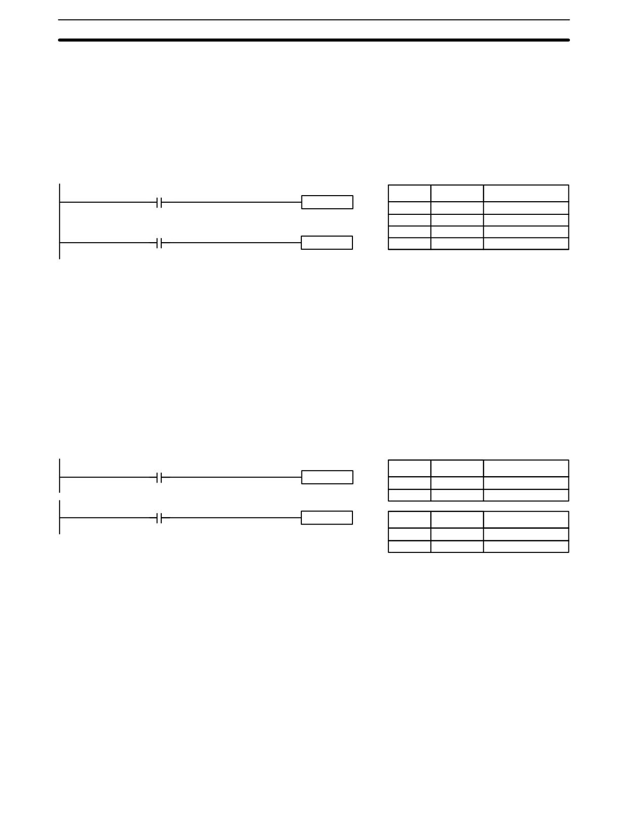
Controlling Bit Status
Section
6-4
SET will turn ON the operand bit when the execution condition goes ON, but un-
like the OUTPUT instruction, SET will not turn OFF the operand bit when the
execution condition goes OFF. RESET will turn OFF the operand bit when the
execution condition goes OFF, but unlike OUTPUT NOT, RESET will not turn ON
the operand bit when the execution condition goes OFF.
In the following example, IR 20000 will be turned ON when IR 00100 goes ON
and will remain ON until IR 00101 goes ON, regardless of the status of IR 00100.
When IR 00101 goes ON, RESET will turn IR 20000 OFF.
00100
Address
Instruction
Operands
SET
20000
00000
LD
00100
00001
SET
20000
00101
00002
LD
00101
RSET 20000
00003
RSET
20000
Note SET and RSET do not have function codes. To input them from the Program-
ming Console, press the FUN and SET Keys or FUN and RSET Keys followed
by the bit address.
6-4-2
DIFFERENTIATE UP and DIFFERENTIATE DOWN
DIFFERENTIATE UP and DIFFERENTIATE DOWN instructions are used to
turn the operand bit ON for one cycle at a time. The DIFFERENTIATE UP
instruction turns ON the operand bit for one cycle after the execution condition
for it goes from OFF to ON; the DIFFERENTIATE DOWN instruction turns ON
the operand bit for one cycle after the execution condition for it goes from ON to
OFF. Both of these instructions require only one line of mnemonic code.
00000
Address
Instruction
Operands
DIFU(13) 20001
00000
LD
00000
00001
DIFU(13)
20001
00001
DIFD(14) 20002
Address
Instruction
Operands
00000
LD
00001
00001
DIFD(14)
20002
Here, IR 20001 will be turned ON for one cycle after IR 00000 goes ON. The next
time DIFU(13) 20001 is executed, IR 20001 will be turned OFF, regardless of the
status of IR 00000. With the DIFFERENTIATE DOWN instruction, IR 20002 will
be turned ON for one cycle after IR 00001 goes OFF (IR 20002 will be kept OFF
until then), and will be turned OFF the next time DIFD(14) 20002 is executed.
6-4-3
KEEP
The KEEP instruction is used to maintain the status of the operand bit based on
two execution conditions. To do this, the KEEP instruction is connected to two
instruction lines. When the execution condition at the end of the first instruction
line is ON, the operand bit of the KEEP instruction is turned ON. When the
execution condition at the end of the second instruction line is ON, the operand
bit of the KEEP instruction is turned OFF. The operand bit for the KEEP instruc-
tion will maintain its ON or OFF status even if it is located in an interlocked sec-
tion of the diagram.
351
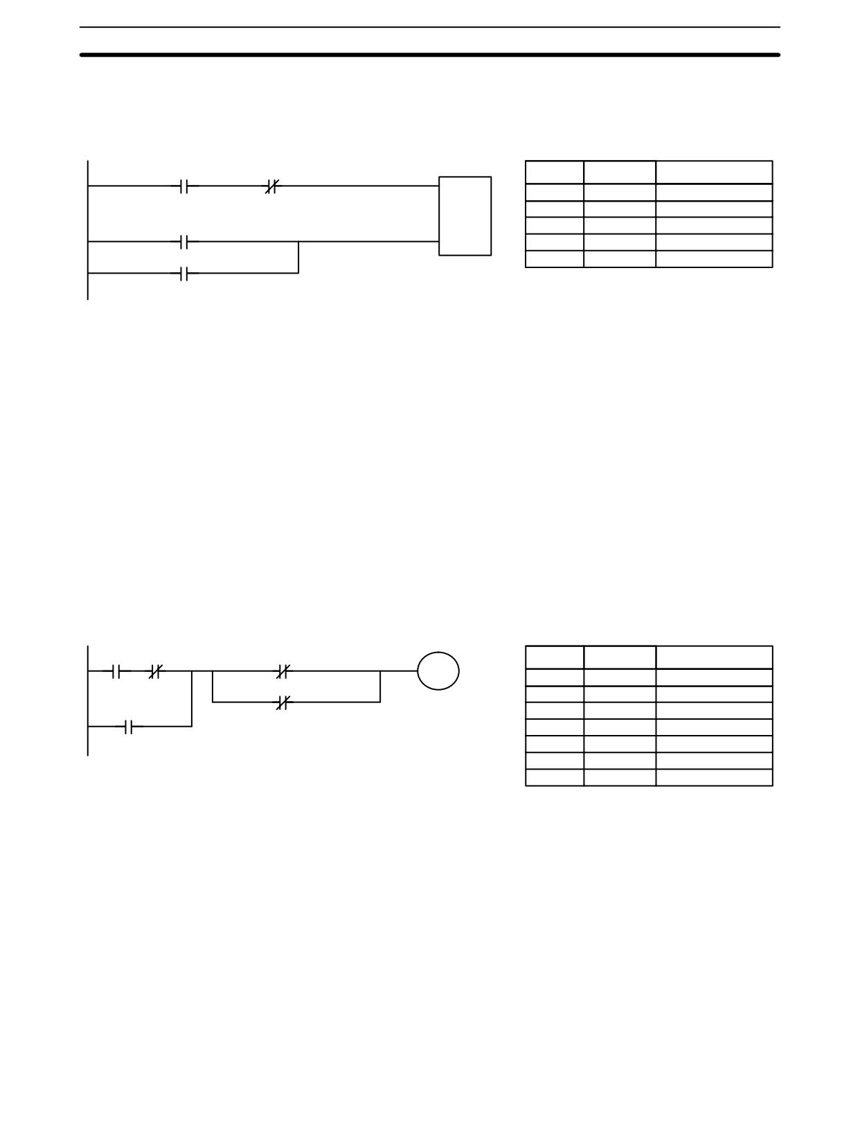
Work Bits (Internal Relays)
Section
6-5
In the following example, HR 0000 will be turned ON when IR 00002 is ON and IR
00003 is OFF. HR 0000 will then remain ON until either IR 00004 or IR 00005
turns ON. With KEEP, as with all instructions requiring more than one instruction
line, the instruction lines are coded first before the instruction that they control.
00002
00003
Address
Instruction
Operands
00000
LD
00002
S: set input
KEEP(11)
00001
AND NOT
00003
HR 0000
00002
LD
00004
00004
00003
OR
00005
R: reset input
00005
00004
KEEP(11)
HR
0000
6-4-4
Self-maintaining Bits (Seal)
Although the KEEP instruction can be used to create self-maintaining bits, it is
sometimes necessary to create self-maintaining bits in another way so that they
can be turned OFF when in an interlocked section of a program.
To create a self-maintaining bit, the operand bit of an OUTPUT instruction is
used as a condition for the same OUTPUT instruction in an OR setup so that the
operand bit of the OUTPUT instruction will remain ON or OFF until changes oc-
cur in other bits. At least one other condition is used just before the OUTPUT
instruction to function as a reset. Without this reset, there would be no way to
control the operand bit of the OUTPUT instruction.
The above diagram for the KEEP instruction can be rewritten as shown below.
The only difference in these diagrams would be their operation in an interlocked
program section when the execution condition for the INTERLOCK instruction
was ON. Here, just as in the same diagram using the KEEP instruction, two reset
bits are used, i.e., HR 0000 can be turned OFF by turning ON either IR 00004 or
IR 00005.
00002
00003
00004
Address
Instruction
Operands
HR 0000
00000
LD
00002
00005
00001
AND NOT
00003
HR 0000
00002
OR
HR
0000
00003
AND NOT
00004
00004
OR NOT
00005
00005
AND LD
---
00006
OUT
HR
0000
6-5
Work Bits (Internal Relays)
In programming, combining conditions to directly produce execution conditions
is often extremely difficult. These difficulties are easily overcome, however, by
using certain bits to trigger other instructions indirectly. Such programming is
achieved by using work bits. Sometimes entire words are required for these pur-
poses. These words are referred to as work words.
Work bits are not transferred to or from the PC. They are bits selected by the
programmer to facilitate programming as described above. I/O bits and other
dedicated bits cannot be used as works bits. All bits in the IR area that are not
allocated as I/O bits, and certain unused bits in the AR area, are available for use
as work bits. Be careful to keep an accurate record of how and where you use
work bits. This helps in program planning and writing, and also aids in debugging
operations.
352
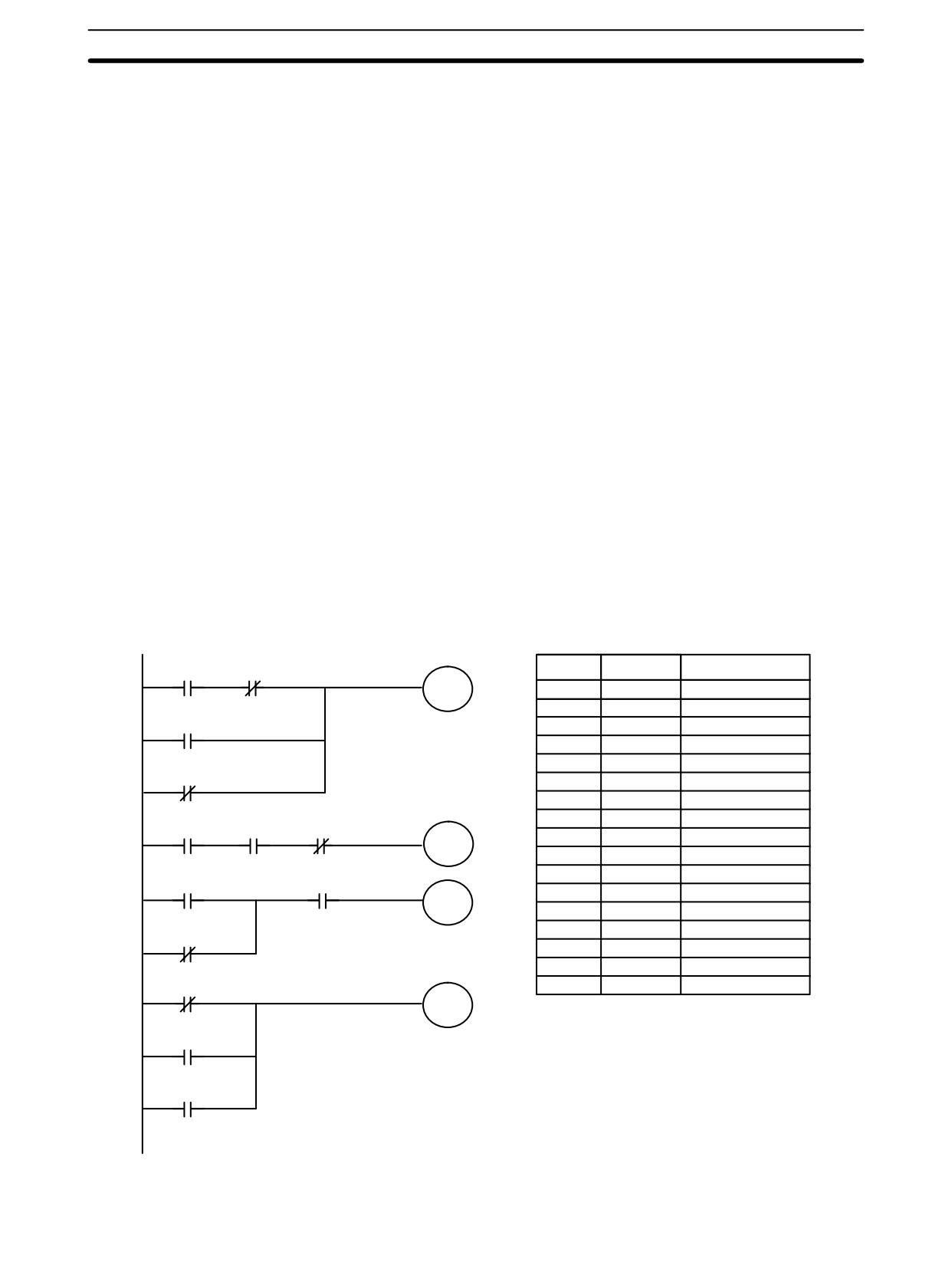
Work Bits (Internal Relays)
Section
6-5
Work Bit Applications
Examples given later in this subsection show two of the most common ways to
employ work bits. These should act as a guide to the almost limitless number of
ways in which the work bits can be used. Whenever difficulties arise in program-
ming a control action, consideration should be given to work bits and how they
might be used to simplify programming.
Work bits are often used with the OUTPUT, OUTPUT NOT, DIFFERENTIATE
UP, DIFFERENTIATE DOWN, and KEEP instructions. The work bit is used first
as the operand for one of these instructions so that later it can be used as a
condition that will determine how other instructions will be executed. Work bits
can also be used with other instructions, e.g., with the SHIFT REGISTER
instruction (SFT(10)). An example of the use of work words and bits with the
SHIFT REGISTER instruction is provided in 7-16-1 SHIFT REGISTER -
SFT(10).
Although they are not always specifically referred to as work bits, many of the
bits used in the examples in Section 7 Instruction Set use work bits. Understand-
ing the use of these bits is essential to effective programming.
Reducing Complex
Work bits can be used to simplify programming when a certain combination of
Conditions
conditions is repeatedly used in combination with other conditions. In the follow-
ing example, IR 00000, IR 00001, IR 00002, and IR 00003 are combined in a
logic block that stores the resulting execution condition as the status of
IR 21600. IR 21600 is then combined with various other conditions to determine
output conditions for IR 20000, IR 20001, and IR 20002, i.e., to turn the outputs
allocated to these bits ON or OFF.
Address
Instruction
Operands
00000
00001
21600
00000
LD
00000
00001
AND NOT
00001
00002
00002
OR
00002
00003
OR NOT
00003
00004
OUT
21600
00003
00005
LD
21600
00006
AND
00004
00007
AND NOT
00005
21600
00004
00005
00008
OUT
20000
20000
00009
LD
21600
00010
OR NOT
00004
21600
00005
00011
AND
00005
20001
00012
OUT
20001
00013
LD NOT
21600
00004
00014
OR
00006
00015
OR
00007
21600
00016
OUT
20002
20002
00006
00007
353
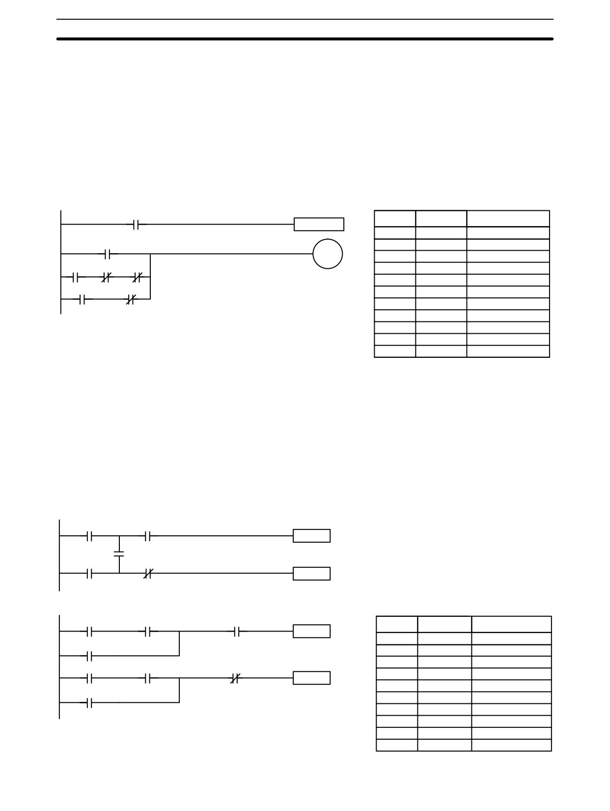
Programming Precautions
Section
6-6
Differentiated Conditions
Work bits can also be used if differential treatment is necessary for some, but not
all, of the conditions required for execution of an instruction. In this example,
IR 20000 must be left ON continuously as long as IR 001001 is ON and both
IR 00002 and IR 00003 are OFF, or as long as IR 00004 is ON and IR 00005 is
OFF. It must be turned ON for only one cycle each time IR 00000 turns ON (un-
less one of the preceding conditions is keeping it ON continuously).
This action is easily programmed by using IR 22500 as a work bit as the operand
of the DIFFERENTIATE UP instruction (DIFU(13)). When IR 00000 turns ON, IR
22500 will be turned ON for one cycle and then be turned OFF the next cycle by
DIFU(13). Assuming the other conditions controlling IR 20000 are not keeping it
ON, the work bit IR 22500 will turn IR 20000 ON for one cycle only.
00000
Address
Instruction
Operands
DIFU(13) 22500
00000
LD
00000
22500
00001
DIFU(13)
22500
20000
00002
LD
22500
00001
00002
00003
00003
LD
00001
00004
AND NOT
00002
00004
00005
00005
AND NOT
00003
00006
OR LD
---
00007
LD
00004
00008
AND NOT
00005
00009
OR LD
---
00010
OUT
20000
6-6
Programming Precautions
The number of conditions that can be used in series or parallel is unlimited as
long as the memory capacity of the PC is not exceeded. Therefore, use as many
conditions as required to draw a clear diagram. Although very complicated dia-
grams can be drawn with instruction lines, there must not be any conditions on
lines running vertically between two other instruction lines. Diagram A shown
below, for example, is not possible, and should be drawn as diagram B. Mne-
monic code is provided for diagram B only; coding diagram A would be impossi-
ble.
00000
00002
Instruction 1
00004
00001
00003
Instruction 2
Diagram A: Not Programmable
00001
00004
00002
Address
Instruction
Operands
Instruction 1
00000
LD
00001
00000
00001
AND
00004
00002
OR
00000
00000
00004
00003
00003
AND
00002
Instruction 2
00004
Instruction 1
00001
00005
LD
00000
00006
AND
00004
Diagram B: Correct Version
00007
OR
00001
00008
AND NOT
00003
00009
Instruction 2
354
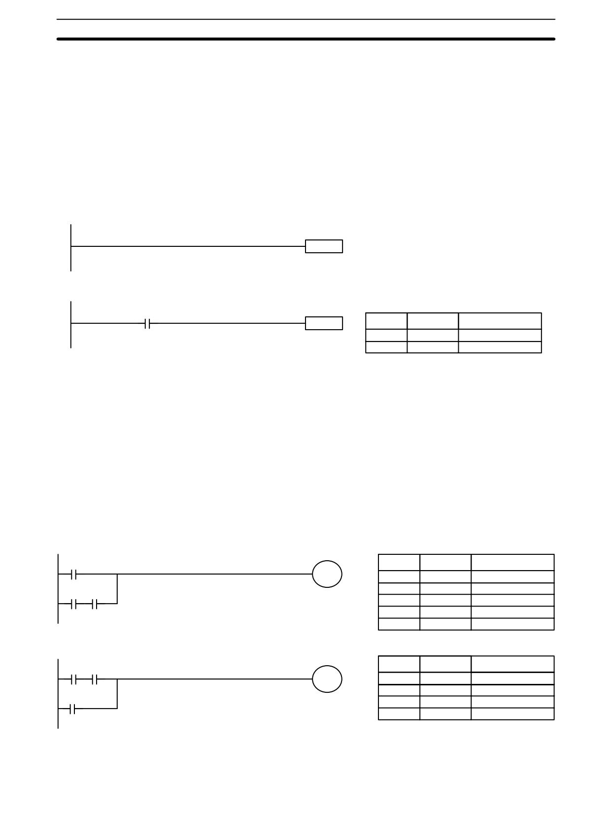
Programming Precautions
Section
6-6
The number of times any particular bit can be assigned to conditions is not lim-
ited, so use them as many times as required to simplify your program. Often,
complicated programs are the result of attempts to reduce the number of times a
bit is used.
Except for instructions for which conditions are not allowed (e.g., INTERLOCK
CLEAR and JUMP END, see below), every instruction line must also have at
least one condition on it to determine the execution condition for the instruction
at the right. Again, diagram A , below, must be drawn as diagram B. If an instruc-
tion must be continuously executed (e.g., if an output must always be kept ON
while the program is being executed), the Always ON Flag (SR 25313) in the SR
area can be used.
Instruction
Diagram A: Not Programmable for Most Instructions
25313
Instruction
Address
Instruction
Operands
00000
LD
25313
Diagram B: Correct Version
00001
Instruction
There are a few exceptions to this rule, including the INTERLOCK CLEAR,
JUMP END, and step instructions. Each of these instructions is used as the se-
cond of a pair of instructions and is controlled by the execution condition of the
first of the pair. Conditions should not be placed on the instruction lines leading to
these instructions. Refer to Section 7 Instruction Set for details.
When drawing ladder diagrams, it is important to keep in mind the number of
instructions that will be required to input it. In diagram A, below, an OR LOAD
instruction will be required to combine the top and bottom instruction lines. This
can be avoided by redrawing as shown in diagram B so that no AND LOAD or OR
LOAD instructions are required. Refer to 7-7-2 AND LOAD and OR LOAD for
more details.
00000
Address
Instruction
Operands
20007
00000
LD
00000
00001
LD
00001
00001
20007
00002
AND
20007
00003
OR LD
---
00004
OUT
20007
Diagram A
Address
Instruction
Operands
00001
20007
20007
00000
LD
00001
00001
AND
20007
00000
00002
OR
00000
00003
OUT
20007
Diagram B
355
Program Execution
Section
6-7
6-7
Program Execution
When program execution is started, the CPU Unit scans the program from top to
bottom, checking all conditions and executing all instructions accordingly as it
moves down the bus bar. It is important that instructions be placed in the proper
order so that, for example, the desired data is moved to a word before that word
is used as the operand for an instruction. Remember that an instruction line is
completed to the terminal instruction at the right before executing an instruction
lines branching from the first instruction line to other terminal instructions at the
right.
Program execution is only one of the tasks carried out by the CPU Unit as part of
the cycle time. Refer to Section 8 PC Operations and Processing Time for de-
tails.
356
SECTION 7
Instruction Set
The CPM1, CPM1A, CPM2A, CPM2C (including the CPM2C-S), and SRM1(-V2) PCs have large programming instruction
sets that allow for easy programming of complicated control processes. This section explains instructions individually and
provides the ladder diagram symbol, data areas, and flags used with each.
The many instructions provided by these PCs are organized in the following subsections by instruction group. These groups
include Ladder Diagram Instructions, instructions with fixed function codes, and set instructions.
Some instructions, such as Timer and Counter instructions, are used to control execution of other instructions, e.g., a TIM
Completion Flag might be used to turn ON a bit when the time period set for the timer has expired. Although these other
instructions are often used to control output bits through the Output instruction, they can be used to control execution of other
instructions as well. The Output instructions used in examples in this manual can therefore generally be replaced by other
instructions to modify the program for specific applications other than controlling output bits directly.
7-1
Notation
360
7-2
Instruction Format
360
7-3
Data Areas, Definer Values, and Flags
360
7-4
Differentiated Instructions
362
7-5
Coding Right-hand Instructions
363
7-6
Instruction Tables
366
7-6-1
CPM1/CPM1A Function Codes
366
7-6-2
CPM2A/CPM2C Function Codes
367
7-6-3
SRM1(-V2) Function Codes
368
7-6-4
Alphabetic List by Mnemonic
369
7-7
Ladder Diagram Instructions
372
7-7-1
LOAD, LOAD NOT, AND, AND NOT, OR, and OR NOT
372
7-7-2
AND LOAD and OR LOAD
373
7-8
Bit Control Instructions
373
7-8-1
OUTPUT and OUTPUT NOT - OUT and OUT NOT
373
7-8-2
SET and RESET - SET and RSET
374
7-8-3
KEEP - KEEP(11)
375
7-8-4
DIFFERENTIATE UP and DOWN - DIFU(13) and DIFD(14)
376
7-9
NO OPERATION - NOP(00)
377
7-10
END - END(01)
377
7-11
INTERLOCK and INTERLOCK CLEAR - IL(02) and ILC(03)
377
7-12
JUMP and JUMP END - JMP(04) and JME(05)
379
7-13
User Error Instructions:
FAILURE ALARM AND RESET - FAL(06) and
SEVERE FAILURE ALARM - FALS(07)
381
7-14
Step Instructions:
STEP DEFINE and STEP START-STEP(08)/SNXT(09)
381
7-15
Timer and Counter Instructions
384
7-15-1
TIMER - TIM
385
7-15-2
HIGH-SPEED TIMER - TIMH(15)
386
7-15-3
VERY HIGH-SPEED TIMER: TMHH(--)
387
7-15-4
LONG TIMER: TIML(--)
388
7-15-5
COUNTER - CNT
390
7-15-6
REVERSIBLE COUNTER - CNTR(12)
391
7-15-7
REGISTER COMPARISON TABLE - CTBL(63)
392
7-15-8
MODE CONTROL - INI(61)
395
7-15-9
HIGH-SPEED COUNTER PV READ - PRV(62)
397
357
7-16
Shift Instructions
400
7-16-1
SHIFT REGISTER - SFT(10)
400
7-16-2
WORD SHIFT - WSFT(16)
401
7-16-3
ARITHMETIC SHIFT LEFT - ASL(25)
401
7-16-4
ARITHMETIC SHIFT RIGHT - ASR(26)
402
7-16-5
ROTATE LEFT - ROL(27)
402
7-16-6
ROTATE RIGHT - ROR(28)
403
7-16-7
ONE DIGIT SHIFT LEFT - SLD(74)
404
7-16-8
ONE DIGIT SHIFT RIGHT - SRD(75)
404
7-16-9
REVERSIBLE SHIFT REGISTER - SFTR(84)
405
7-16-10 ASYNCHRONOUS SHIFT REGISTER - ASFT(17)
406
7-17
Data Movement Instructions
407
7-17-1
MOVE - MOV(21)
407
7-17-2
MOVE NOT - MVN(22)
408
7-17-3
BLOCK TRANSFER - XFER(70)
409
7-17-4
BLOCK SET - BSET(71)
410
7-17-5
DATA EXCHANGE - XCHG(73)
411
7-17-6
SINGLE WORD DISTRIBUTE - DIST(80)
411
7-17-7
DATA COLLECT - COLL(81)
413
7-17-8
MOVE BIT - MOVB(82)
415
7-17-9
MOVE DIGIT - MOVD(83)
416
7-18
Data Control Instructions
417
7-18-1
SCALING - SCL(66)
417
7-18-2
SIGNED BINARY TO BCD SCALING - SCL2(--)
418
7-18-3
BCD TO SIGNED BINARY SCALING - SCL3(--)
420
7-18-4
PID CONTROL - PID(--)
422
7-19
Comparison Instructions
428
7-19-1
COMPARE - CMP(20)
428
7-19-2
TABLE COMPARE - TCMP(85)
429
7-19-3
BLOCK COMPARE - BCMP(68)
430
7-19-4
DOUBLE COMPARE - CMPL(60)
432
7-19-5
AREA RANGE COMPARE - ZCP(--)
433
7-19-6
DOUBLE AREA RANGE COMPARE - ZCPL(--)
434
7-20
Conversion Instructions
435
7-20-1
BCD-TO-BINARY - BIN(23)
435
7-20-2
BINARY-TO-BCD - BCD(24)
436
7-20-3
DOUBLE BCD-TO-DOUBLE BINARY - BINL(58)
436
7-20-4
DOUBLE BINARY-TO-DOUBLE BCD - BCDL(59)
437
7-20-5
4-TO-16 DECODER - MLPX(76)
438
7-20-6
16-TO-4 ENCODER - DMPX(77)
440
7-20-7
7-SEGMENT DECODER - SDEC(78)
442
7-20-8
ASCII CONVERT - ASC(86)
445
7-20-9
ASCII-TO-HEXADECIMAL - HEX(--)
447
7-20-10 HOURS-TO-SECONDS - SEC(--)
449
7-20-11 SECONDS-TO-HOURS - HMS(--)
450
7-20-12 2’S COMPLEMENT - NEG(--)
451
7-21
BCD Calculation Instructions
453
7-21-1
SET CARRY - STC(40)
453
7-21-2
CLEAR CARRY - CLC(41)
453
7-21-3
BCD ADD - ADD(30)
453
7-21-4
BCD SUBTRACT - SUB(31)
454
7-21-5
BCD MULTIPLY - MUL(32)
456
7-21-6
BCD DIVIDE - DIV(33)
457
7-21-7
DOUBLE BCD ADD - ADDL(54)
458
7-21-8
DOUBLE BCD SUBTRACT - SUBL(55)
460
7-21-9
DOUBLE BCD MULTIPLY - MULL(56)
462
7-21-10 DOUBLE BCD DIVIDE - DIVL(57)
462
358
7-22
Binary Calculation Instructions
463
7-22-1
BINARY ADD - ADB(50)
463
7-22-2
BINARY SUBTRACT - SBB(51)
464
7-22-3
BINARY MULTIPLY - MLB(52)
466
7-22-4
BINARY DIVIDE - DVB(53)
466
7-23
Special Math Instructions
467
7-23-1
DATA SEARCH - SRCH(--)
467
7-23-2
FIND MAXIMUM - MAX(--)
468
7-23-3
FIND MINIMUM - MIN(--)
470
7-23-4
AVERAGE VALUE - AVG(--)
472
7-23-5
SUM - SUM(--)
474
7-24
Logic Instructions
475
7-24-1
COMPLEMENT - COM(29)
475
7-24-2
LOGICAL AND - ANDW(34)
476
7-24-3
LOGICAL OR - ORW(35)
477
7-24-4
EXCLUSIVE OR - XORW(36)
477
7-24-5
EXCLUSIVE NOR - XNRW(37)
478
7-25
Increment/Decrement Instructions
479
7-25-1
BCD INCREMENT - INC(38)
479
7-25-2
BCD DECREMENT - DEC(39)
479
7-26
Subroutine Instructions
480
7-26-1
SUBROUTINE ENTER - SBS(91)
480
7-26-2
SUBROUTINE DEFINE and RETURN - SBN(92)/RET(93)
482
7-26-3
MACRO - MCRO(99)
482
7-27
Pulse Output Instructions
483
7-27-1
SET PULSES - PULS(65)
483
7-27-2
SPEED OUTPUT- SPED(64)
485
7-27-3
ACCELERATION CONTROL - ACC(--)
487
7-27-4
PULSE WITH VARIABLE DUTY RATIO - PWM(--)
490
7-27-5
SYNCHRONIZED PULSE CONTROL - SYNC(--)
492
7-28
Special Instructions
493
7-28-1
MESSAGE DISPLAY - MSG(46)
493
7-28-2
I/O REFRESH - IORF(97)
494
7-28-3
BIT COUNTER - BCNT(67)
495
7-28-4
FRAME CHECKSUM - FCS(--)
496
7-29
Interrupt Control Instructions
497
7-29-1
INTERRUPT CONTROL - INT(89)
497
7-29-2
INTERVAL TIMER - STIM(69)
500
7-30
Communications Instructions
501
7-30-1
RECEIVE - RXD(47)
501
7-30-2
TRANSMIT - TXD(48)
503
7-30-3
CHANGE RS-232C SETUP - STUP(--)
505
359
Data Areas, Definer V
alues, and Flags
Section
7-3
7-1
Notation
In the remainder of this manual, all instructions will be referred to by their mne-
monics. For example, the OUTPUT instruction will be called OUT; the AND
LOAD instruction, AND LD. If you’re not sure of the instruction a mnemonic is
used for, refer to Appendix A Programming Instructions.
If an instruction is assigned a function code, it will be given in parentheses after
the mnemonic. These function codes, which are 2-digit decimal numbers, are
used to input most instructions into the CPU Unit. A table of instructions listed in
order of function codes is also provided in Appendix A Programming Instruc-
tions. Lists of instructions are also provided in 7-6 Instruction Tables.
An @ before a mnemonic indicates the differentiated version of that instruction.
Differentiated instructions are explained in Section 7-4.
7-2
Instruction Format
Most instructions have at least one or more operands associated with them. Op-
erands indicate or provide the data on which an instruction is to be performed.
These are sometimes input as the actual numeric values (i.e., as constants), but
are usually the addresses of data area words or bits that contain the data to be
used. A bit whose address is designated as an operand is called an operand bit;
a word whose address is designated as an operand is called an operand word. In
some instructions, the word address designated in an instruction indicates the
first of multiple words containing the desired data.
Each instruction requires one or more words in Program Memory. The first word
is the instruction word, which specifies the instruction and contains any definers
(described below) or operand bits required by the instruction. Other operands
required by the instruction are contained in following words, one operand per
word. Some instructions require up to four words.
A definer is an operand associated with an instruction and contained in the same
word as the instruction itself. These operands define the instruction rather than
telling what data it is to use. Examples of definers are TC numbers, which are
used in timer and counter instructions to create timers and counters, as well as
jump numbers (which define which Jump instruction is paired with which Jump
End instruction). Bit operands are also contained in the same word as the
instruction itself, although these are not considered definers.
7-3
Data Areas, Definer Values, and Flags
In this section, each instruction description includes its ladder diagram symbol,
the data areas that can be used by its operands, and the values that can be used
as definers. Details for the data areas are also specified by the operand names
and the type of data required for each operand (i.e., word or bit and, for words,
hexadecimal or BCD).
Not all addresses in the specified data areas are necessarily allowed for an oper-
and, e.g., if an operand requires two words, the last word in a data area cannot
be designated as the first word of the operand because all words for a single op-
erand must be within the same data area. Other specific limitations are given in a
Limitations subsection. Refer to Section 5 Memory Areas for addressing con-
ventions and the addresses of flags and control bits.
!
Caution The IR and SR areas are considered as separate data areas. If an operand has
access to one area, it doesn’t necessarily mean that the same operand will have
access to the other area. The border between the IR and SR areas can, howev-
er, be crossed for a single operand, i.e., the last bit in the IR area may be speci-
fied for an operand that requires more than one word as long as the SR area is
also allowed for that operand.
360
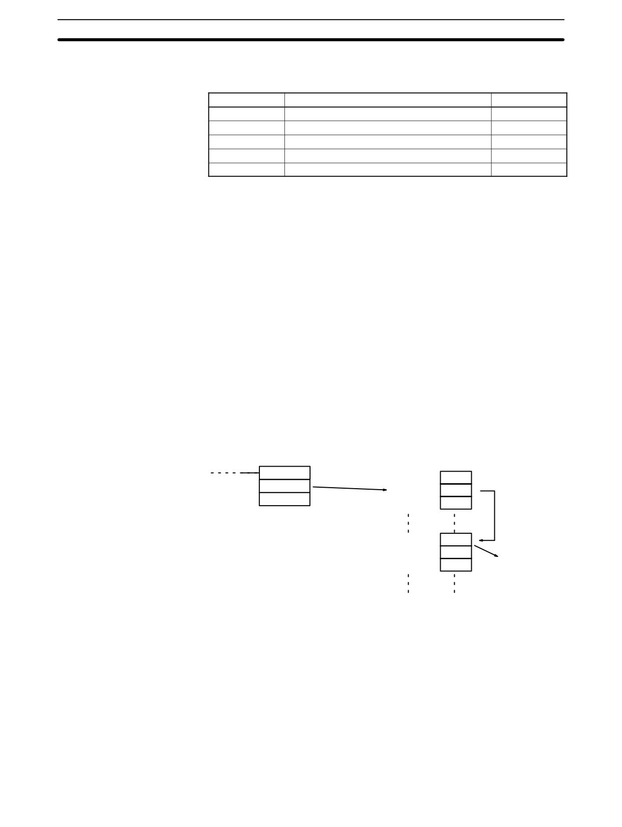
Data Areas, Definer V
alues, and Flags
Section
7-3
The Flags subsection lists flags that are affected by execution of an instruction.
These flags include the following SR area flags.
Abbreviation
Name
Bit
ER
Instruction Execution Error Flag
25503
CY
Carry Flag
25504
GR
Greater Than Flag
25505
EQ
Equals Flag
25506
LE
Less Than Flag
25507
ER is the flag most commonly used for monitoring an instruction’s execution.
When ER goes ON, it indicates that an error has occurred in attempting to
execute the current instruction. The Flags subsection of each instruction lists
possible reasons for ER being ON. ER will turn ON if operands are not entered
correctly. Instructions are not executed when ER is ON. A table of instructions
and the flags they affect is provided in Appendix B Error and Arithmetic Flag Op-
eration.
When the DM area is specified for an operand, an indirect address can be used.
Indirect Addressing
Indirect DM addressing is specified by placing an asterisk before the DM: *DM.
When an indirect DM address is specified, the designated DM word will contain
the address of the DM word that contains the data that will be used as the oper-
and of the instruction. If, for example, *DM 0001 was designated as the first op-
erand and LR 00 as the second operand of MOV(21), the contents of DM 0001
was 1111, and DM 1111 contained 5555, the value 5555 would be moved to
LR 00.
Word
Content
MOV(21)
DM 0000
4C59
*DM 0001
DM 0001
1111
LR 00
Indirect
Indicates
DM 0002
F35A
address
DM 1111.
DM 1111
5555
DM 1113
2506
5555 moved
DM 1114
D541
to LR 00.
When using indirect addressing, the address of the desired word must be in BCD
and it must specify a word within the DM area. In the above example, the content
of DM 0001 has to be in BCD and has to specify an address in the DM area of the
PC being used. (Refer to Section 5 Memory Areas for DM area details.)
Although data area addresses are most often given as operands, many oper-
Designating Constants
ands and all definers are input as constants. The available value range for a giv-
en definer or operand depends on the particular instruction that uses it.
Constants must also be entered in the form required by the instruction, i.e., in
BCD or in hexadecimal.
361
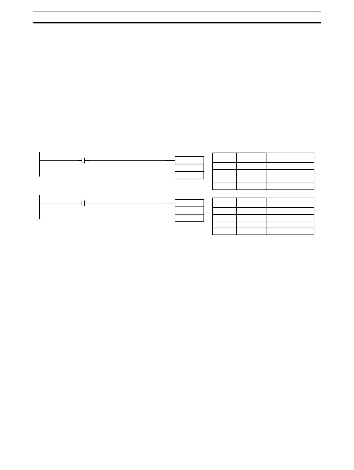
Differentiated Instructions
Section
7-4
7-4
Differentiated Instructions
Most instructions are provided in both differentiated and non-differentiated
forms. Differentiated instructions are distinguished by an @ in front of the
instruction mnemonic.
A non-differentiated instruction is executed each time it is scanned as long as its
execution condition is ON. A differentiated instruction is executed only once af-
ter its execution condition goes from OFF to ON. If the execution condition has
not changed or has changed from ON to OFF since the last time the instruction
was scanned, the instruction will not be executed. The following two examples
show how this works with MOV(21) and @MOV(21), which are used to move the
data in the address designated by the first operand to the address designated by
the second operand.
00000
Address
Instruction
Operands
MOV(21)
00000
LD
00000
HR 10
00001
MOV(21)
Diagram A
DM 0000
HR
10
DM
0000
00000
@MOV(21)
Address
Instruction
Operands
HR 10
00000
LD
00000
Diagram B
DM 0000
00001
@MOV(21)
HR
10
DM
0000
In diagram A, the non-differentiated MOV(21) will move the content of HR 10 to
DM 0000 whenever it is scanned with 00000. If the cycle time is 80 ms and 00000
remains ON for 2.0 seconds, this move operation will be performed 25 times and
only the last value moved to DM 0000 will be preserved there.
In diagram B, the differentiated @MOV(21) will move the content of HR 10 to DM
0000 only once after 00000 goes ON. Even if 00000 remains ON for 2.0 seconds
with the same 80 ms cycle time, the move operation will be executed only once
during the first cycle in which 00000 has changed from OFF to ON. Because the
content of HR 10 could very well change during the 2 seconds while 00000 is
ON, the final content of DM 0000 after the 2 seconds could be different depend-
ing on whether MOV(21) or @MOV(21) was used.
All operands, ladder diagram symbols, and other specifications for instructions
are the same regardless of whether the differentiated or non-differentiated form
of an instruction is used. When inputting, the same function codes are also used,
but NOT is input after the function code to designate the differentiated form of an
instruction. Most, but not all, instructions have differentiated forms.
Refer to 7-11 INTERLOCK and INTERLOCK CLEAR - IL(02) and IL(03) for the
effects of interlocks on differentiated instructions.
The CPM2A/CPM2C also provides differentiation instructions: DIFU(13) and
DIFD(14). DIFU(13) operates the same as a differentiated instruction, but is
used to turn ON a bit for one cycle. DIFD(14) also turns ON a bit for one cycle, but
does it when the execution condition has changed from ON to OFF. Refer to
7-8-4 DIFFERENTIATE UP and DOWN - DIFU(13) and DIFD(14) for details.
362
Coding Right-hand Instructions
Section
7-5
7-5
Coding Right-hand Instructions
Writing mnemonic code for ladder instructions is described in Section 6 Ladder-
diagram Programming. Converting the information in the ladder diagram symbol
for all other instructions follows the same pattern, as described below, and is not
specified for each instruction individually.
The first word of any instruction defines the instruction and provides any defin-
ers. If the instruction requires only a signal bit operand with no definer, the bit
operand is also placed on the same line as the mnemonic. All other operands are
placed on lines after the instruction line, one operand per line and in the same
order as they appear in the ladder symbol for the instruction.
The address and instruction columns of the mnemonic code table are filled in for
the instruction word only. For all other lines, the left two columns are left blank. If
the instruction requires no definer or bit operand, the data column is left blank for
first line. It is a good idea to cross through any blank data column spaces (for all
instruction words that do not require data) so that the data column can be quickly
scanned to see if any addresses have been left out.
If an IR or SR address is used in the data column, the left side of the column is left
blank. If any other data area is used, the data area abbreviation is placed on the
left side and the address is placed on the right side. If a constant to be input, the
number symbol (#) is placed on the left side of the data column and the number
to be input is placed on the right side. Any numbers input as definers in the
instruction word do not require the number symbol on the right side. TC bits,
once defined as a timer or counter, take a TIM (timer) or CNT (counter) prefix.
When coding an instruction that has a function code, be sure to write in the func-
tion code, which will be necessary when inputting the instruction via the Pro-
gramming Console. Also be sure to designate the differentiated instruction with
the @ symbol.
Note The mnemonics of expansion instructions are followed by “(--)” as the function
code to indicate that they must be assigned function codes by the user in the
instructions table before they can be used in programming. Refer to page 156 for
details.
363
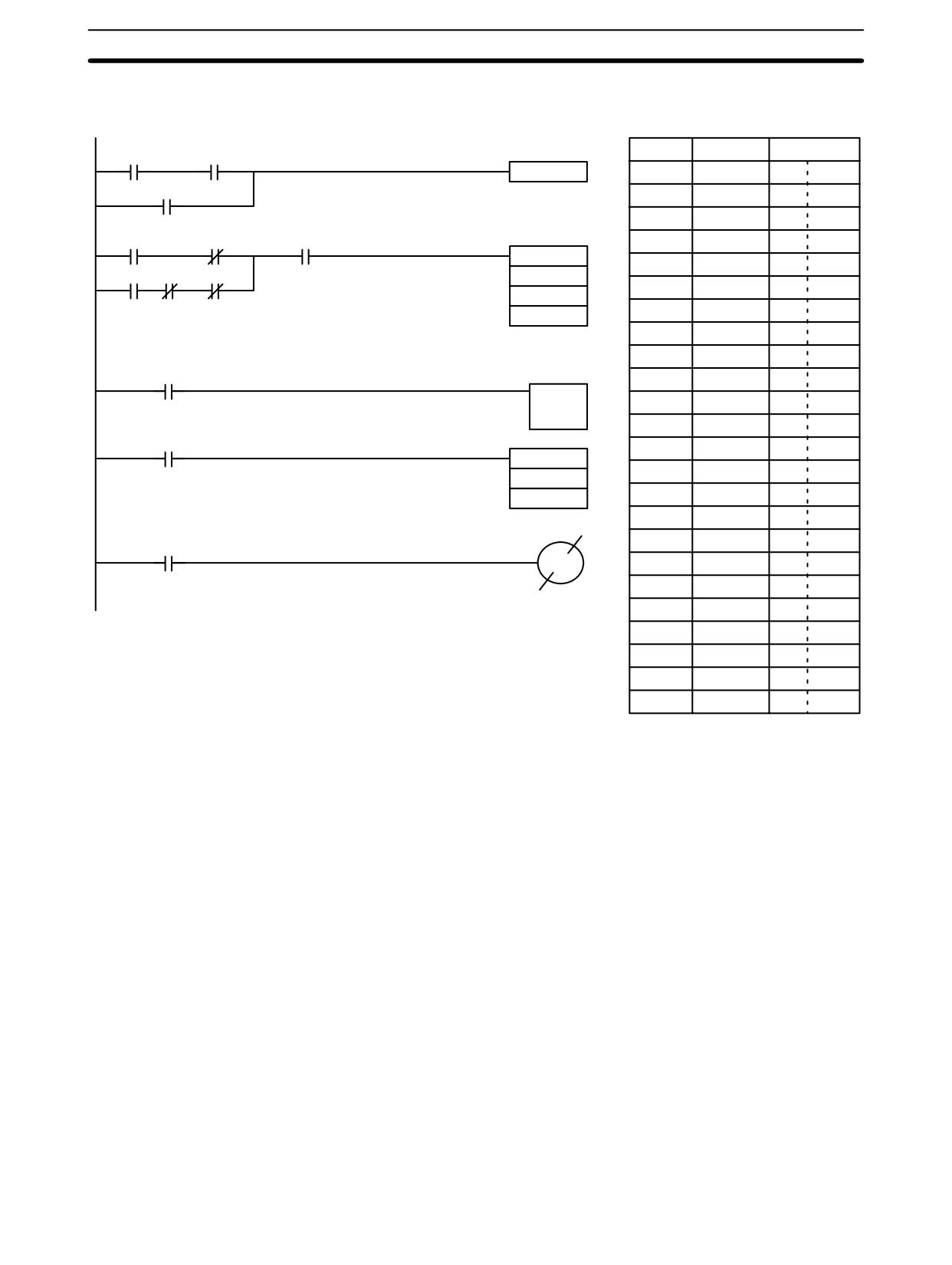
Coding Right-hand Instructions
Section
7-5
The following diagram and corresponding mnemonic code illustrates the points
described previously.
Address
Instruction
Data
00000
00001
DIFU(13) 21600
00000
LD
00000
00002
00001
AND
00001
00002
OR
00002
00100
00200
21600
00003
DIFU(13)
21600
BCNT(67)
00004
LD
00100
01001
01002
LR 0000
#0001
00005
AND NOT
00200
004
00006
LD
01001
HR 00
00007
AND NOT
01002
00008
AND NOT
LR
0000
00005
00009
OR LD
--
TIM 000
00010
AND
21600
#0150
00011
BCNT(67)
--
TIM 000
#
0001
MOV(21)
004
HR 00
HR
00
LR 00
00012
LD
00005
00013
TIM
000
HR 0015
01000
#
0150
00014
LD
TIM
000
00015
MOV(21)
--
HR
00
LR
00
00016
LD
HR
0015
00017
OUT NOT
01000
364
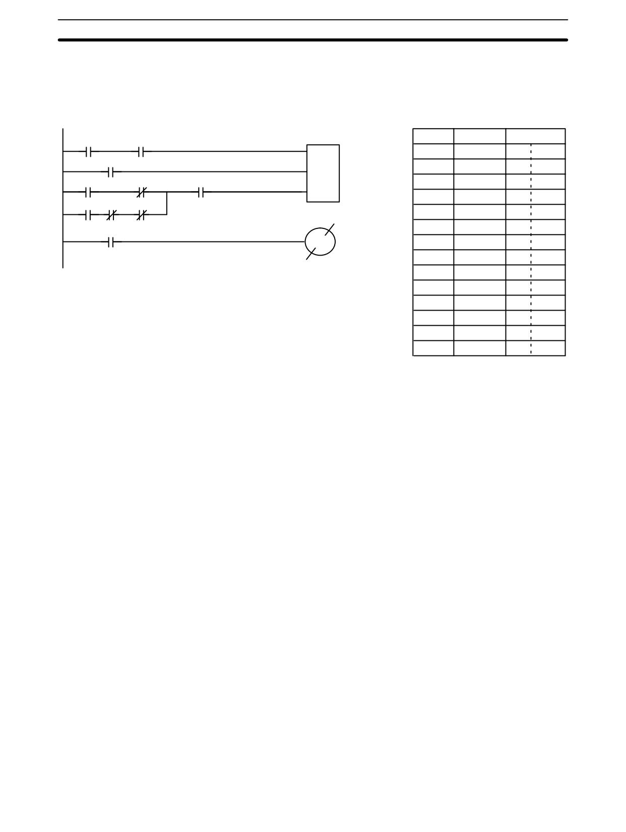
Coding Right-hand Instructions
Section
7-5
Multiple Instruction Lines
If a right-hand instruction requires multiple instruction lines (such as KEEP(11)),
all of the lines for the instruction are entered before the right-hand instruction.
Each of the lines for the instruction is coded, starting with LD or LD NOT, to form
‘logic blocks’ that are combined by the right-hand instruction. An example of this
for SFT(10) is shown below.
Address
Instruction
Data
00000
00001
I
00000
LD
00000
SFT(10)
00002
P
00001
AND
00001
HR 00
00100
00200
21600
00002
LD
00002
R
HR 00
00003
LD
00100
01001
01002
LR 0000
00004
AND NOT
00200
00005
LD
01001
HR 0015
01001
00006
AND NOT
01002
00007
AND NOT
LR
0000
00008
OR LD
--
00009
AND
21600
00010
SFT(10)
HR
00
HR
00
00011
LD
HR
0015
00012
OUT NOT
01001
365