Loongson 7A1000 Bridge User Manual. Loongson Technology Corporation Limited Version 2.00 - page 5
Bit Field
Name
Length
Read/Write
Description
7
dlab
1
R/W
Crossover latch access bits
1: Access to operate the divider latch.
0: Access to operate the normal register.
R/W
Interrupt control bit
6
bcb
1
1: The output of the serial port is set to 0 (interrupt
state) at this time.
0: Normal operation.
5
spb
1
R/W
Specify the parity bit
0: No parity bit is specified.
1: If the LCR[4] bit is 1, the transmit and check
parity bit is 0. If the LCR[4] bit is 0, the transmit and
check parity bit is 1. If the LCR[4] bit is 0, then the
transmit and check parity bit is 1.
R/W
Parity Bit Selection
4
eps
1
0: Odd number of 1’s per character (including data
and parity bits).
1: Even 1’s in each character.
3
pe
1
R/W
Parity bit enable
0: No parity bit.
1: Parity bit is generated at output, and parity bit is
judged at input.
2
sb
1
R/W
Define the number of bits to generate stop bits
0: 1 stop bit.
1: 1.5 stop bits at 5-bit character length, 2 stop
bits at other lengths.
1:0
bec
2
R/W
Set the number of bits per character
00b: 5 bits.
01b: 6 bits.
10b: 7 bits.
11b: 8 bits.
MODEM control register (MCR)
Offset:`0x04`
119
Reset value:`0x00`
Table 160. MODEM control register (MCR)
Bit Field
Name
Length
Read/Write
Description
W
Reserved
7:5
Reserved
3
4
Loop
1
W
Loopback mode control bits
0: Normal operation.
1: Loopback mode.
In loopback mode, the TXD output is always 1 and
the output shift register is connected directly to the
input shift register. Other connections are as
follows: DTR - DSR RTS - CTS Out1 - RI Out2 - DCD
W
Connects to the DCD input in loopback mode
3
OUT2
1
2
OUT1
1
W
Connects to the RI input in loopback mode
W
RTS signal control bit
1
RTSC
1
W
DTR signal control bit
0
DTRC
1
Line status register (LSR)
Offset:`0x05`
Reset value:`0x00`
Table 161. Line status register (LSR)
Bit Field
Name
Length
Read/Write
Description
R
Error indication bit
7
ERROR
1
0: No errors.
1: At least one of parity bit error, frame error or
interrupt interrupt. one.
R
Transfer to empty indicates bit
6
TE
1
0: Data is available.
1: Both the transmit FIFO and the transmit shift
register are empty. Clear when writing data to the
transfer FIFO is cleared when writing data to the
FIFO.
5
TFE
1
R
Transfer FIFO bit null indicates bit
0: Data is available.
1: The current transmit FIFO is empty and is cleared
when writing data to the transmit FIFO.
120
Bit Field
Name
Length
Read/Write
Description
4
BI
1
R
Interrupt interrupt indication bit
0: No interrupt.
1: Received Start bit + data + parity bit + stop bit are
0, i.e., there is an interrupt interrupt .
3
FE
1
R
Frame error indication bits 0: There are no errors. 1:
The received data has no stop bit.
R
Parity bit error indication bit
2
PE
1
0: There is no parity error.
1: There is a parity error in the current received data.
1
OE
1
R
Data overflow indication bit
0: No overflow.
1: There is data overflow.
R
Receive data valid indication bit
0
DR
1
0: No data in the FIFO.
1: There is data in the FIFO.
When reading this register, LSR[4:1] and LSR[7] are cleared to zero, LSR[6:5] is cleared when writing data to
the transmit FIFO, and LSR[0] is judged for the receive FIFO.
MODEM status register (MSR)
Offset: 0x06
Reset value: 0x00
Table 162. MODEM status register (MSR)
Bit Field
Name
Length
Read/Write
Description
7
CDCD
1
R
The inverse of the DCD input value, or to Out2 in
loopback mode
R
The inverse of the RI input value, or to OUT1 in
6
CRI
1
loopback mode
5
CDSR
1
R
The inverse of the DSR input value, or to DTR in
loopback mode
R
4
CCTS
1
The inverse of the CTS input value, or to RTS in
loopback mode
R
DDCD indication bit
3
DDCD
1
R
2
TERI
1
RI edge detection, RI state changes from low to
high
R
DDSR indication bit
1
DDSR
1
121
Bit Field
Name
Length
Read/Write
Description
0
DCTS
1
R
DCTS indication bit
Frequency divider latch
Offset: 0x00
Reset value: 0x00
Table 163. Frequency divider latch 1
Bit Field
Name
Length
Read/Write
Description
R/W
7:0
LSB
8
Store the lower 8 bits of the divider latch
Offset:0x01
Reset value:0x00
Table 164. Frequency divider latch 2
Bit Field
Name
Length
Read/Write
Description
R/W
7:0
MSB
8
Store the high 8 bits of the divider latch
The value of the crossover latch {MSB,LSB} is calculated as 50MHz/16/baud rate. For example, if you
want to configure a serial port baud rate of 115200, the value of the divider latch = 50,000,000/16/115,200
≈ 27.
122
Chapter 10. I2C Controller
A total of 6 I2C controllers are integrated into the bridge, and the I2C controllers operate at 50MHz. The
maximum transfer rate supported by the I2C bus is 400kbps.
10.1. Access Address and Pin Multiplexing
The base address of accessing the I2C controller is the base address of the MISC low-speed device block
plus an offset of 0x10000.
Note: The I2C module only supports access by 1 byte.
The physical address composition of the I2C module internal registers is as follows.
Table 165. The physical address composition of the I2C module internal registers
Address bits
Composition
Note
Reserved
[15:11]
0
I2C controller number
[10:8]
0x0-0x5 represent I2C0-I2C5 respectively
Reserved
[7:3]
0
[2:0]
REG
Internal registers address
For I2C modules, the corresponding pins should be set to the corresponding functions when used. The pin
settings related to I2C are described in Pin Multiplexing Configuration Register.
10.2. Description of I2C Controller Register
Frequency Division Latch Low-order Byte Register (PRERlo)
Offset: 0x00
Reset value: 0xff
Table 166. Frequency division latch low-order byte register
Bit Field
Name
Length
Read/Write
Description
7:0
PRERlo
8
R/W
Store the lower 8 bits of the division
latch
Frequency Division Latch High-order Byte Register (PRERhi)
Offset: 0x01
Reset value: 0xff
Table 167. Frequency division latch high-order byte register
Bit Field
Name
Length
Read/Write
Description
RW
7:0
PRERhi
8
Store the high 8 bits of the division
latch
Assuming that the value of the divider latch is Prescaler and the frequency of the I2C controller is 50MHz,
123
if the clock frequency of the
I2C
bus
is needed clock_s, then Prescaler should
be
equal
to:
50M/(5*clock_s) - 1.
Control Register (CTR)
Offset: 0x02
Reset value: 0x00
Table 168. Control register
Bit Field
Name
Length
Read/Write
Description
7
EN
1
R/W
Module enable bit
0: Module disable
1: Module enable
6
IEN
1
R/W
Interrupt enable bit
0: Interrupt disable
1: Interrupt enable
R/W
Reserved
5:0
Reserved
6
Transport Data Register (TXR)
Offset: 0x03
Reset value: 0x00
Table 169. Transport data register
Bit Field
Name
Length
Read/Write
Description
W
When transporting data, the data to be
7:1
DATA[7:1]/ADDR
7
sent (bit[7:1]) is stored.
When transporting the address, the
address of the I2C slave device is
stored
0
DATA[0]/RW
1
W
When transporting data, stores the
data to be sent (bit[0]).
When transporting the address, the
read and write status is stored.
0: Write
1: Read
Receive Data Register (RXR)
Offset: 0x03
124
Reset value: 0x00
Table 170. Receive data register
Bit Field
Name
Length
Read/Write
Description
7:0
RXR
8
R
Store received data
Command Control Register (CR)
Offset: 0x04
Reset value: 0x00
Table 171. Command control register
Bit Field
Name
Length
Read/Write
Description
W
7
STA
1
Generate the START signal
W
6
STO
1
Generate the STOP signal
W
Generate the read signal
5
RD
1
W
Generate the write signal
4
WR
1
3
ACK
1
W
Generate the response signal
0: The controller sends ack at the end
of this transmission
1: The controller does not send ack at
the end of this transmission
2:1
Reserved
2
W
Reserved
W
Generate interrupt response signal.
0
IACK
1
Software writes 1 to this bit to clear
the interrupt.
State Register (SR)
Offset: 0x04
Reset value: 0x00
Table 172. State register
Bit Field
Name
Length
Read/Write
Description
7
RxACK
1
R
Receive response bit
1 - no receive the response bit
0 - receive the response bit
6
Busy
1
R
I2c bus busy flag bit
1 - bus is busy
0 - bus is free
125
Bit Field
Name
Length
Read/Write
Description
5
AL
1
R
When the I2C core loses control of the
I2C bus, this bit is 1
4:2
Reserved
3
R
Reserved
R
Indicate the process of transport
1
TIP
1
1 - indicate that data is being
transported
0 - indicate that data transport is
complete
R
Interrupt flag bit. When one data
0
IF
1
transport is finished, or another device
initiates data transport, this bit is 1
126
Chapter 11. PWM Controller
A four-way pulse width output/counter controller (PWM) is implemented in the bridge. The four PWMs The
four PWMs work and control in exactly the same way. Each PWM pin can be used as either a pulse output
signal or a pulse width measurement input signal. The PMW controller clock is 50MHz, and the count and
reference registers are 32-bit length.
11.1. Access Address and Pin Multiplexing
The base address of accessing the PWM controller is the base address of the MISC low-speed device block
plus an offset of 0x20000.
Note: The PWM module only supports access by 4 bytes.
The physical address composition of the PWM controller internal registers is as follows.
Table 173. The physical address composition of the PWM controller internal registers
Address bits
Composition
Note
Reserved
[15:10]
0
[9:8]
PWM number
0x0-0x3 represent PWM0-PWM3 respectively
[7:4]
0
Reserved
[3:0]
REG
Internal registers address
For PMM modules, the corresponding pins should be set to the corresponding functions when used. The
pin settings related to PMM are described in Pin Multiplexing Configuration Register.
11.2. Description of Registers
There are three registers per controller, which are described as follows.
Table 174. List of PWM registers
Name
Address
Length
Read/Write
Description
R/W
Low pulse width register
low_buffer
Base + 0x4
32
full_buffer
Base + 0x8
32
R/W
Pulse period width register
R/W
Control register
CTRL
Base + 0xC
11
PWM Control Register Configuration
Bit Field
Name
Read/Write
Reset Value
Description
0
EN
R/W
0
PWM enable bit
1: PWM enable
0: PWM disable
R/W
Reserved
2:1
Reserved
0
127
Bit Field
Name
Read/Write
Reset Value
Description
3
OE
R/W
0
Pin pulse output enable control bit
(active low). When set to 1, the PWM
can be used as a periodic interrupt
generation module without changing
the value of the PWM pin (held at 0)
0: Pulse output enable
1: Pulse output disable
4
SINGLE
R/W
0
Single pulse control bit, valid for non-
measurement mode
1: Pulse is generated only once
0: Pulse is generated continuously
R/W
Interrupt enable bit. In the non-
5
INTE
0
measurement mode, an interrupt is
generated for every pulse period
measured. In the measurement mode,
an interrupt is generated when the
input pulse period is greater than
0xFFFF_FFF9.
1: Interrupt is generated
0: No interrupt is generated
R/W
6
INT
0
Interrupt status bit. Write 1 to this bit
to clear the interrupt
1: The interrupt is generated
0: No interrupt
7
RST
R/W
0
Counter reset
1: Reset
0: Normal work
8
CAPTE
R/W
0
Measurement pulse enable
1: Measurement pulse mode
0: Non-measurement pulse mode (or
pulse output mode in general)
128
Bit Field
Name
Read/Write
Reset Value
Description
9
INVERT
R/W
0
Output invert enable, valid for non-
measurement mode
1: Invert the signal after the pulse is
output (period starts at high level)
0: Keeps the pulse at the original
output (period starts at low level)
10
DZONE
R/W
0
Anti dead zones function enable, valid
for non-measurement mode
1: This PWM enables the anti dead
zones function
0: This PWM disables the anti dead
zones function
11.3. Description of Functions
11.3.1. Pulse Width Modulation Function
The low_buffer and full_buffer registers are used to configure the low level of the periodic signal
and the length of the total period of the PWM output in the clock period of the PWM module (20ns),
respectively. For example, to generate a low pulse width of 50 times the PWM module clock period and a
high pulse width of 90 times the PWM module clock period, you should configure the value 50 in the
low_buffer and (50+90)=140 in the full_buffer.
The pulse width register value should be written before the CTRL control register. Before writing a new
number to the pulse width register, you should clear the EN bit in the control register and then set the EN bit
to 1 after writing the new number.
If
0 is written to both buffer registers, the output is always low. If writing 0 to low_buffer and 1 to
full_buffer, the output is always high. If the value written to low_buffer is not less than the value of
full_buffer, the output is low.
11.3.2. Pulse Measurement Function
After setting the CTRL control register, the PWM continuously samples the input signal level. When a down-
jump of the input pulse signal is detected, the internal counter starts counting from 1, and when an up-jump
is detected, the counter value is shifted to the low_buffer register and continues to accumulate, and
when a down-jump is detected again, the counter value is shifted to the full_buffer register. For
example, if the input pulse is 50 times the low pulse width of the system clock and 90 times the high pulse
width, the final value read in the low_buffer is 50, and the value read in the full_buffer register is
(50+90)=140.
It should be noted that the pulse to be measured should be a periodic signal, and the pulse period should
not exceed the range that the 32-bit counter can measure. If there is a pulse with a pulse period longer than
0xFFFF_FFF9, the INT bit of the control register will be set to 1, indicating that the pulse to be measured
is out of the measurement range.
129
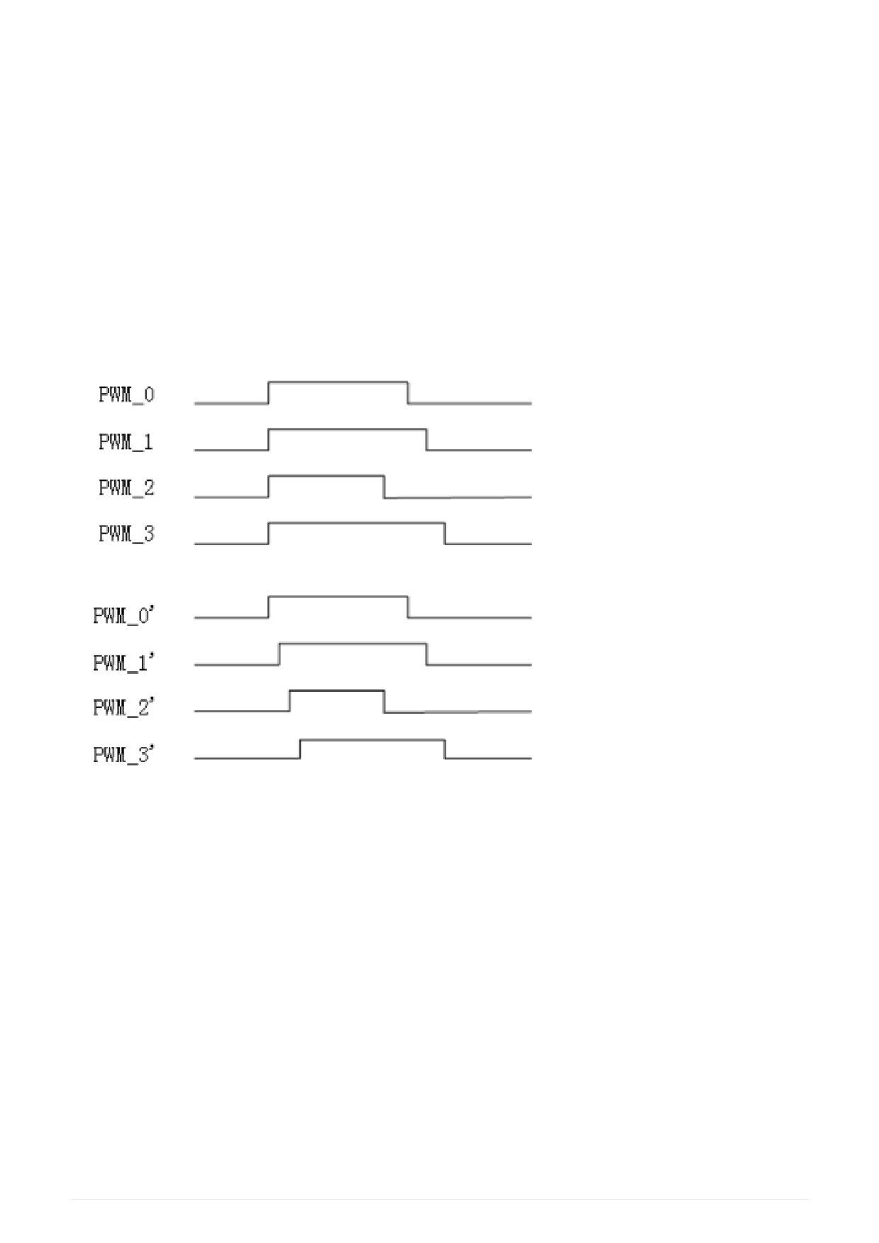
11.3.3. Anti Dead Zones Function
Multiple PWMs are equipped with an anti dead zones function between them, which prevents multiple pulse
outputs from jumping at the same time. To use the anti dead zones function, the multiple PWMs of the anti
dead zones function must be numbered from 0 and be consecutive, and their anti dead zones functions
must all be enabled. In other words, one of PWM0/1, PWM0/1/2 and PWM0/1/2/3 must be used when using
the anti dead zones function.
For PWM_0, PWM_1, PWM_2, and PWM_3, their priority is 0> 1 > 2 > 3. If they jump at the same time, PWM_1
will jump only after PWM_0 jumps (the lower priority signal is “erased” by one clock cycle), and so on. This
priority is fixed and cannot be changed.
A typical anti dead zones example is as follows (PWM_* is the output when the anti dead zones function is
disabled, and PWM_*' is the output when the anti dead zones function is enabled).
Figure 8. Anti dead zones function
130
Chapter 12. Power Management Module (ACPI
Support)
Bridge power management module provides system power management functions. It supports Advanced
Configuration and Power Interface, Version 4.0a (ACPI) to provide the corresponding power management
functions.
• System hibernation and wake-up, support for ACPI S3 (suspend to RAM), ACPI S4 (suspend to disk),
ACPI S5 (soft off), and support for power failure detection and automatic system recovery. It also
supports multiple wake-up methods (USB, GMAC, power switch, etc.)
• System clock control, module clock gating, multiple ways to adjust the frequency.
•
It integrates a watchdog with a maximum timing time of about 82s.
12.1. Access Address
The base address of accessing the power management module is the base address of the MISC low-speed
device block plus an offset of 0x50000.
Note: The PWM module only supports access by 4 bytes.
The physical address composition of the ACPI module internal registers is as follows.
Table 175. The physical address composition of the ACPI controller internal registers
Address bits
Composition
Note
[15:8]
0
Reserved
Internal registers address
[7:0]
REG
12.2. Power Level
Table 176. Description of ACPI status
Work all. The system works all in this mode
G0/S0
Not supported at the moment
G1/S1
Suspend to RAM (STR). Context saving to memory
G1/S3
Suspend to Disk (STD). Save to hard disk, except wake-up circuit all power
G1/S4
down
Soft off. Only the wake-up circuit is powered on
G2/S5
Mechanical off. All power supply failures
G3
12.3. Description of Registers
This section describes the power management related registers. The register voltage field indicates the
voltage field to which this bit of the register belongs.
PMCON_SOC: SOC General PM Configuration Register
Table 177. SOC general PM configuration register
Address Offset
Voltage Field
Attribute
131
0x00
SOC
R/W, RO
Bit Field
Description
25
PWRBTN_LVL - RO
This bit indicates the current PWRBTNn signal status.
24
PWRTYP - RO
This bit indicates the power supply mode.
1: AC (Adapter)
0: Battery
23:0
Reserved
PMCON_RESUME : RESUME General PM Configuration Register
Table 178. RESUME general PM configuration register
Address Offset
Voltage Field
Attribute
0x04
RESUME
R/W, RO, R/WC
Bit Field
Description
Reserved
31:14
13
VSB_GATEn_EN - R/W
Enables or disables the VSB_GATEn function.
0: off; 1: enable.
If RSMRSTn is active, this bit is 1. This bit is configured by the system after re-powering.
If the motherboard uses the VSB_GATEn pin as the power management control signal,
the system software must write 1 to this bit.
12:11
VSB_GATEn_DLY - R/W
Used to control the duration of the VSB_GATEn signal relative to S3n from S0 to S3 and
S3 to S0 (the time advanced when sleeping and the time delayed when waking up).
2’b00: 31.25ms advance at hibernation and 125ms delay at wake-up.
2’b01: 62.5ms advance at hibernation, 250ms delay at wake-up.
2’b10: 125ms advance on hibernation and 500ms delay on wake-up.
2’b11: 250ms ahead of hibernation and 1s behind wake-up.
This field is 2’b0 if RSMRSTn is valid, and is configured by the system after re-powering.
Reserved
10:8
132
7
USB_GMAC_OK - R/W
If RSMRSTn is valid, this bit is 0, indicating that USB and GMAC are not configured and
cannot wake up the system. The system will configure this bit after re-powering.
6
CTT_STS - R/WC
The system enters the G2/S5 state when a temperature trip occurs in the S0 state, and
this bit is used to detect the logged event status after re-powering the system.
5
CTT_EN - R/W
Enable the temperature trip protection mechanism.
4
LID_OPEN - RO
Display status detection bit.
1: Display is on.
0: Display is off.
3
Reserved
2
SRS (System Reset Status) - R/WC
0: SYS_RESETn has not been pressed
1: SYS_RESETn has been pressed. This bit should be checked after system reset and
clear it accordingly.
1
PWROK_FLR (PWROK Failure) - R/WC
When the system is in the S0 state, the PWROK signal becomes invalid and this bit is set
to 1. Software writes 1 to clear this bit.
0
DRAM_INIT - R/W
This bit does not affect the hardware function, PMON will set this bit to 1 before DRAM
initialization, and write 0 to this bit after finishing DRAM initialization, software can use
this bit to check if DRAM initialization has been interrupted.
PMCON_RTC : RTC General PM Configuration Register
Table 179. RTC general PM configuration register
Address Offset
Voltage Field
Attribute
0x08
RTC
R/W, R/WC
Bit Field
Description
Reserved
31:9
133
8
WOL_EN - R/W
Controls whether the SLPLANn signal is active when the system is in the low-power
state. When the system is in the operating state, SLPLANn is held high.
0: SLPLANn is not valid.
1: SLPLANn is pulled low if the system is powered by the power supply. If the system is
powered by the battery, WOL_BAT_EN determines whether SLPLANn is pulled low.
7
WOL_BAT_EN - R/W
When the system enters a low-power state and is battery powered and WOL_EN is high.
0: SLPLANn is invalid.
1: SLPLANn is pulled low.
6:5
S3_ASSERTION_WIDTH - R/W
The 2 bits represent the minimum time interval between when the S3n signal is valid
and when it is invalid again.
11: 1s
10: 125ms
01: 1ms
00: 60us
4:3
S4_ASSERTION_WIDTH - R/W
The 2 bits represent the minimum time interval between when the S4n signal is valid
and when it is invalid again.
11: 4s
10: 2s
01: 1s
00: 125us
2
S4_ASSERTION_EN - R/W
0: The interval between valid and re-invalidation of the S4n signal is several RTC
periods.
1: The interval between valid and re-invalidation of the S4n signal is determined by
S4_ASSERTION_WIDTH.
134
1
PWR_FLR (Power Failure) - R/WC
This bit is in the RTC domain and can only be reset by RTC_RSTn.
1 indicates that a power failure has occurred in the system (entering the G3 state), i.e.,
all power supplies except RTC have failed (RSMRSTn has been active). The software
clears this bit by writing 1.
0
AFTERG3_EN - R/W
This bit determines the action of the system after it enters the G3 state and the power is
restored.
0: The system will automatically revert to the S0 state after power is restored.
1: The system will revert to the S5 state, or if the system was in the S4 state when the
power failure occurred, the system will revert to the S4 state after power is restored.
This bit will be set to 1 by the power button override and thermal trip events.
PM1_STS : Power Management 1 Status Register
Table 180. Power Management 1 Status Register
Address Offset
Voltage Field
Attribute
0x0C
RESUME/RTC/SOC
R/WC
Bit Field
Description
Voltage Field
Reserved
31:16
15
WAK_STS (Wake Status) - R/WC
Resume
0: Software writes 1 to clear this bit.
1: Hardware writes 1 to this bit if the system is woken up from any of
the sleep states by a wakeup event.
14
PCIEXP_WAKE_STS - R/WC
Resume
1: PCIE wake-up event occurs
0: Software write 1 to clear the bit
13:12
Reserved
11
PRBTNOR_STS (Power Button Override Status) - R/WC
RTC
0: Software writes 1 to clear this bit.
1: When power button override occurs, this bit is set to 1, the system
enters G2/S5 unconditionally state, while setting AFTERG3_EN to 1.
135
10
RTC_STS (RTC Status) - R/WC
Resume
0: Software writes 1 to clear this bit.
1: This bit is 1 when the RTC generates an alarm. Also when RTC_EN
is valid, this bit generates a wake-up event.
Reserved
9
8
PWRBTN_STS (Power Button Status) - R/WC
Resume
0: Software writes 1 to clear this bit. Thermal trip will clear this bit.
1: This bit will be set to 1 when PWRBTNn is pressed and held for more
than 16ms (less than 4s). In the S0 state, an interrupt is generated
when both PWRBTN_EN and PWRBTN_STS are active. During any sleep
state from S3-S5, the system will resume if PWRBTN_STS is set.
7:1
Reserved
0
TMROF_STS (PM Timer Overflow Status) - R/WC 0: Software writes 1
SOC
to clear this bit.
1: When the highest bit of the 24-bit counter (20ns per clock cycle) is
inverted, this bit is set to 1. The timer function is recommended to be
done with HPET.
PM1_EN: Power Management 1 Enable Register
Table 181. Power management 1 enable register
Address Offset
Voltage Field
Attribute
R/W
0x10
RESUME/RTC/SOC
Bit Field
Description
Voltage Field
Reserved
31:15
14
PCIEXP_WAKE_DIS - R/W
resume
When this bit is set, no PCIE wake-up event is generated, but the value
of this bit does not affect the value of PCIEXP_WAKE_STS.
Reserved
13:11
10
RTC_EN (RTC Event Enable) - R/W
rtc
RTC wake-up and interrupt enable.
Reserved
9
8
PWRBTN_EN (Power Button Enable) - R/W
resume
PWRBTN interrupt event generation enable, this bit does not affect
PWRBTN wake-up event generation.
Reserved
7:1
136
0
TMROF_EN (PM Timer Overflow Enable) - R/W
SOC
If this bit is set, TMROF_STS will generate an interrupt.
PM1_CNT: Power Management 1 Control Register
Table 182. Power management 1 control register
Address Offset
Voltage Field
Attribute
0x14
RESUME/RTC/SOC
R/W
Bit Field
Description
Voltage Field
Reserved
31:14
13
SLP_EN (Sleep Enable) - R/W
resume
Writing 1 to this bit will cause the system to enter the SLP_TYP
declared hibernation state, and this bit will automatically revert to 0
upon entering the associated hibernation state.
12:10
SLP_TYP (Sleep Type) - R/W
rtc
This 3 bits indicate the hibernation state of the system.
000: S0 state.
001: Reserved.
010: Reserved.
011: Reserved.
100: Reserved.
101: Suspend-to-RAM. S3n signal is valid, enter S3 state.
110: Suspend-to-Disk. S3n, S4n signals are valid, enter S4 state.
111: Soft Off. S3n, S4n, S5n signals are valid, enter S5 state.
9:1
Reserved
0
INT_EN - R/W
SOC
Interrupt enable switch to enable the generation of interrupt signals
for the power management controller.
PM1_TMR: Power Management 1 Timer
Table 183. Power management 1 timer
Address Offset
Voltage Field
Attribute
0x18
SOC
RO
Bit Field
Description
Reserved
31:24
137
23:0
TMR_VAL (Timer Value) - RO
Counter counts with a period of 8ns. When the 23 bit is inverted, the TNROF_STS bit is
set. HPET is recommended.
GPE0_STS: General Purpose Event0 Status Register
Table 184. General purpose event0 status register
Address Offset
Voltage Field
Attribute
R/WC
0x28
RESUME
Bit Field
Description
31:16
Reserved
15:10
USB[5:0]_STS - R/WC
Only the bit 10 is meaningful, the 15:11 bits are meaningless for now.
0: Software writes 1 to clear this bit.
1: These bits are set when a USB wake event occurs, and when the USBx_EN bit is valid,
a wake event or interrupt is generated.
9
Reserved
8
RI_STS - R/WC
0: Software writes 1 to clear this bit.
1: This bit is set when the RIn signal is valid.
7
BATLOW_STS - R/WC
0: Software writes 1 to clear this bit.
1: This bit is set when the BATLOWn signal is active.
If BATLOW_EN is valid, an interrupt will be generated when BATLOW_STS is set. This bit
does not generate a wake-up event.
6
GMAC1_STS - R/WC
0: Software writes 1 to clear this bit.
1: These bits are set when a wake event occurs in GMAC1 and generate a wake event or
interrupt when the GMAC1_EN bit is valid.
5
GMAC0_STS - R/WC
0: Software writes 1 to clear this bit.
1: These bits are set when a wake event occurs in GMAC0 and generate a wake event or
interrupt when the GMAC0_EN bit is valid.
138
4
LID_STS - R/WC
0: Software writes 1 to clear this bit.
1: When the LID_EN bit is valid, a wake-up event is generated.
3
CTW_STS - R/WC
Thermal warning is generated.
2
CTA_STS - R/WC
Thermal alert is generated.
1
PWRSWITCH_STS - R/WC
The PWRTYP changes when the power supply status changes. This bit generates an
interrupt.
Reserved
0
GPE0_EN: General Purpose Event0 Enable Register
Table 185. General purpose event0 enable register
Address Offset
Voltage Field
Attribute
R/W
0x2C
RESUME/RTC
Bit Field
Description
Voltage Field
31:16
Reserved
15:10
USB[5 :0]_EN - R/W
0: Invalid.
1: Enable USBx_STS to wake-up event that will generate an interrupt
signal when returning to S0.
Reserved
9
8
RI_EN - R/W
RTC
0: Invalid.
1: Enable RIn_STS wake-up event that will generate an interrupt
signal when returning to S0.
7
BATLOW_EN - R/W
RTC
0: Invalid.
1: Enable BATLOWn interrupt event.
139
6
GMAC1_EN - R/W
RTC
0: Invalid.
1: Enable GMAC1_STS wake-up event, which will generate an interrupt
signal when returning to S0.
5
GMAC0_EN - R/W
0: Invalid.
1: Enable GMAC0_STS wake-up event, which will generate an interrupt
signal when returning to S0.
4
LID_EN - R/W
0: Invalid.
1: Enable LID_STS wake-up event, and an interrupt signal will be
generated when S0 state.
3
CTW_EN - R/W
Enable THERMAL WARNING interrupt.
2
CTA_EN - R/W
Enable THERMAL ALERT interrupt.
1
PWRSWITCH_EN - R/W
Enable PWRSWITCH_STS interrupt.
0
LID_POL - R/W
This bit sets the polarity of the LID.
RST_CNT: Reset Control Register
Table 186. Reset control register
Address Offset
Voltage Field
Attribute
R/W
0x30
SOC
Bit Field
Description
Reserved
31:2
1
WD_EN - R/W
Watch dog function enable.
0
OS_RST - R/W
Software writes this bit to reset the system.
WD_SET : Watch Dog Set Register
Table 187. Watch dog set register
140
Address Offset
Voltage Field
Attribute
0x34
SOC
WO
Bit Field
Description
Reserved
31:1
0
When WD_EN is 1, writing this bit will refill the internal watch dog counter with the value
of WD_Timer. Note that the watch dog counter operates at 50MHz.
WD_Timer: Watch Dog Timer Register
Table 188. Watch dog timer register
Address Offset
Voltage Field
Attribute
R/W
0x38
SOC
Bit Field
Description
31:0
The value of this register is the watch dog refill value, and the reset value is all 1s.
GEN_RTC_1: General RTC Register 1
Table 189. General RTC register 1
Address Offset
Voltage Field
Attribute
R/W
0x50
RTC
Bit Field
Description
31:0
RTC general purpose register.
GEN_RTC_2: General RTC Register 2
Table 190. General RTC register 2
Address Offset
Voltage Field
Attribute
0x54
RTC
R/W
Bit Field
Description
RTC general purpose register.
31:0
141
Chapter 13. RTC
The Real Time Clock (RTC) unit can be configured when the motherboard is powered up, and when the
motherboard is powered down, the unit still operates and can run normally on the on-board battery power
alone. The RTC unit operates with only a few microamps of current.
The RTC contains an oscillator, which in combination with an external 32.768KHZ crystal generates the
operating clock. This clock is used for time information maintenance and is used to maintain time
information and to generate various timing and counting interrupts.
The RTC module contains two counters, the TOY (Time of Year) counter and the RTC counter. The TOY
counter counts in years, months, hours, minutes and seconds with an accuracy of 0.1s. The RTC counter
counts at 32.768KHz and is 32-bit length.
13.1. Access Address
The base address of accessing the RTC module is the base address of the MISC low-speed device block
plus an offset of 0x50100.
Note: The RTC module only supports access by 4 bytes.
The physical address composition of the RTC module internal registers is as follows.
Table 191. The physical address composition of the RTC module internal registers
Address bits
Composition
Note
[15:9]
0
Reserved
[8]
1
Reserved
Internal registers address
[7:0]
REG
13.2. Description of Registers
Table 192. List of RTC registers
Name
Offset
Length
Read/Write
Description
address
R/W
sys_toytrim
0x20
32
Software must initialize it to 0
WO
TOY low 32 bits input
sys_toywrite0
0x24
32
WO
TOY high 32 bits input
sys_toywrite1
0x28
32
sys_toyread0
0x2C
32
RO
TOY low 32 bits output
RO
TOY high 32 bits output
sys_toyread1
0x30
32
R/W
TOY timer interrupt 0
sys_toymatch0
0x34
32
sys_toymatch1
0x38
32
R/W
TOY timer interrupt 1
R/W
TOY timer interrupt 2
sys_toymatch2
0x3C
32
R/W
TOY and RTC control registers
sys_rtcctrl
0x40
32
Software must initialize them
R/W
sys_rtctrim
0x60
32
Software must initialize it to 0
142
Name
Offset
Length
Read/Write
Description
address
WO
RTC timer counter input
sys_rtcwrite0
0x64
32
sys_rtcread0
0x68
32
RO
RTC timer counter output
R/W
RTC clock timer interrupt 0
sys_rtcmatch0
0x6C
32
R/W
RTC clock timer interrupt 1
sys_rtcmatch1
0x70
32
sys_rtcmatch2
0x74
32
R/W
RTC clock timer interrupt 2
13.2.1. SYS_TOYWRITE0
Address Offset: 24-27h
Attribute: WO
Default value: N/A
Size: 4
Table 193. SYS_TOYWRITE0
Bit Field
Name
Read/Write
Description
WO
31:26
TOY_MONTH
Month, range 1-12
WO
25:21
TOY_DAY
Day, range 1-31
20:16
TOY_HOUR
WO
Hour, range 0-23
15:10
TOY_MIN
WO
Minute, range 0-59
WO
9:4
TOY_SEC
Second, range 0-59
WO
3:0
TOY_MILLISEC
0.1 Second, range 0-9
13.2.2. SYS_TOYWRITE1
Address Offset: 28-2Bh
Attribute: WO
Default value: N/A
Size: 4
Table 194. SYS_TOYWRITE1
Bit Field
Name
Read/Write
Description
WO
31:0
TOY_YEAR
Year, range 0-16383
13.2.3. SYS_TOYREAD0
Address Offset: 2C-2Fh
Attribute: RO
143
Default value: 00000000h
Size: 4
Table 195. SYS_TOYREAD0
Bit Field
Name
Read/Write
Description
31:26
TOY_MONTH
RO
Month, range 1-12
RO
25:21
TOY_DAY
Day, range 1-31
RO
20:16
TOY_HOUR
Hour, range 0-23
RO
15:10
TOY_MIN
Minute, range 0-59
9:4
TOY_SEC
RO
Second, range 0-59
3:0
TOY_MILLISEC
RO
0.1 Second, range 0-9
13.2.4. SYS_TOYREAD1
Address Offset: 30-33h
Attribute: RO
Default value: 00000000h
Size: 4
Table 196. SYS_TOYREAD1
Bit Field
Name
Read/Write
Description
RO
31:0
TOY_YEAR
Year, range 0-16383
13.2.5. SYS_TOYMATCH0
Address Offset: 34-37h
Attribute: R/W
Default value: 00000000h
Size: 4
Table 197. SYS_TOYMATCH0
Bit Field
Name
Read/Write
Description
R/W
31:26
YEAR
Year, range 0-16383
R/W
25:22
MONTH
Month, range 1-12
R/W
21:17
DAY
Day, range 1-31
R/W
16:12
HOUR
Hour, range 0-23
11:6
MIN
R/W
Minute, range 0-59
144
Bit Field
Name
Read/Write
Description
5:0
SEC
R/W
Second, range 0-59
13.2.6. SYS_TOYMATCH1
Address Offset: 38-3Bh
Attribute: R/W
Default value: 00000000h
Size: 4
Table 198. SYS_TOYMATCH1
Bit Field
Name
Read/Write
Description
R/W
31:26
YEAR
Year, range 0-16383
R/W
25:22
MONTH
Month, range 1-12
21:17
DAY
R/W
Day, range 1-31
16:12
HOUR
R/W
Hour, range 0-23
R/W
11:6
MIN
Minute, range 0-59
R/W
5:0
SEC
Second, range 0-59
13.2.7. SYS_TOYMATCH2
Address Offset: 3C-3Fh
Attribute: R/W
Default value: 00000000h
Size: 4
Table 199. SYS_TOYMATCH2
Bit Field
Name
Read/Write
Description
31:26
YEAR
R/W
Year, range 0-16383
R/W
25:22
MONTH
Month, range 1-12
R/W
21:17
DAY
Day, range 1-31
R/W
16:12
HOUR
Hour, range 0-23
R/W
11:6
MIN
Minute, range 0-59
5:0
SEC
R/W
Second, range 0-59
13.2.8. SYS_RTCCTRL
Address Offset: 40-43h
145
Attribute: RO, R/W
Default value: 00000000h
Size: 4
Table 200. SYS_RTCCTRL
Bit Field
Name
Read/Write
Description
RO
Reserved
31:24
Reserved
RO
23
ERS
REN (bit 13) write status
RO
Reserved
22:21
Reserved
20
RTS
RO
Sys_rtctrim write status
RO
19
RM2
Sys_rtcmatch2 write status
RO
18
RM2
Sys_rtcmatch2 write status
RO
17
RM0
Sys_rtcmatch0 write status
RO
16
RS
Sys_rtcwrite write status
15:14
Reserved
RO
Reserved
R/W
RTC enable (active high).
13
REN
Needs to be initialized to 1
RO
Reserved
12
Reserved
11
TEN
R/W
TOY enable (active high).
Needs to be initialized to 1
10:9
Reserved
RO
Reserved
R/W
8
EO
0: 32.768k crystal oscillation disable
1: 32.768k crystal oscillation enable
RO
Reserved
7:6
Reserved
RO
5
Status
32K crystal oscillation work state.
0: 32.768k crystal oscillation not work
1: 32.768k crystal oscillation working
properly
4
Reserved
RO
Reserved
RO
3
TM2
Sys_toymatch2 write state
2
TM1
RO
Sys_toymatch1 write state
1
TM0
RO
Sys_toymatch0 write state
0
TS
RO
Sys_toywrite write state
146
13.2.9. SYS_RTCWRITE
Address Offset: 64-67h
Attribute: WO
Default value: N/A
Size: 4
Table 201. SYS_RTCWRITE
Bit Field
Name
Read/Write
Description
WO
RTC counter input register
31:0
RTCWRITE
13.2.10. SYS_RTCREAD
Address Offset: 68-6Bh
Attribute: RO
Default value: 00000000h
Size: 4
Table 202. SYS_RTCREAD
Bit Field
Name
Read/Write
Description
RO
RTC counter output register
31:0
RTCREAD
13.2.11. SYS_RTCMATCH0
Address Offset: 6C-6Fh
Attribute: R/W
Default value: 00000000h
Size: 4
Table 203. SYS_RTCMATCH0
Bit Field
Name
Read/Write
Description
31:0
RTCMATCH0
R/W
RTC timer comparison register 0
13.2.12. SYS_RTCMATCH1
Address Offset: 70-73h
Attribute: R/W
Default value: 00000000h
147
Size: 4
Table 204. SYS_RTCMATCH1
Bit Field
Name
Read/Write
Description
31:0
RTCMATCH1
R/W
RTC timer comparison register 1
13.2.13. SYS_RTCMATCH2
Address Offset: 74-77h
Attribute: R/W
Default value: 00000000h
Size: 4
Table 205. SYS_RTCMATCH2
Bit Field
Name
Read/Write
Description
R/W
RTC timer comparison register 2
31:0
RTCMATCH2
148
Chapter 14. GPIO
The bridge chip has 57 GPIO pins, GPIO00 is a dedicated GPIO pin, and the remaining 56 are multiplexed
with other functions. Each GPIO pin is controlled by a set of control registers, including: GPIO direction
control (GPIO_OEN), GPIO output (GPIO_O), GPIO input (GPIO_I), and GPIO input interrupt enable control
(GPIO_INT_EN).
Table 206. GPIO control register
Register
Size (bit)
Description
GPIO_OEN
1
GPIO output enable (active low).
GPIO_O
1
GPIO output.
GPIO input.
GPIO_I
1
GPIO_INT_EN
1
GPIO interrupt enable.
14.1. Access Address
The base address of accessing the GPIO module is the base address of the MISC low-speed device block
plus an offset of 0x60000.
Note: The GPIO module only supports access by 1 byte.
The bridge chip provides two ways to control the GPIO pins. One is to control each GPIO pin by bit and the
other is to control each GPIO pin by byte. The bridge chip does this by providing two address spaces to
map the GPIO control registers. One is a per-bit mapping and the other is a per-byte indexing of each bit of
the control register. Correspondingly, the GPIO internal address space is divided into two parts.
The latter way is recommended for the GPIO controller pins.
The physical address composition of the GPIO module internal registers is as follows.
Table 207. The physical address composition of the GPIO module internal registers
Address space
Description
Address of byte control register
0x800-0xC00
Address of bit control register
0x0-0x40
Table 208. Address of GPIO bit control configuration register
Address Offset
Register
Size (bit)
Description
0x00
GPIO_OEN
57
GPIO output enable (active low). Each bit controls
one GPIO pin.
GPIO output. Each bit controls one GPIO pin.
0x10
GPIO_O
57
GPIO input. Each bit controls one GPIO pin.
0x20
GPIO_I
57
0x30
GPIO_INT_EN
57
GPIO interrupt enable. Each bit controls one GPIO
pin.
Table 209. Address of GPIO byte control configuration register
149