Loongson 7A1000 Bridge User Manual. Loongson Technology Corporation Limited Version 2.00 - page 3
Table 34. Pcie h phy lo access configuration register 2
Bit Field
Name
Read/Write
Description
31:7
Reserved
R/W
Reserved
R/W
PHY Configuration Reset, High Active
6
phy_cfg_reset
RO
PHY Configuration Status Machine Status
5:3
phy_cfg_state
Indication
2
phy_cfg_done
R/W
The completion of one access to PHY
indicates the completion of reading and
writing to PHY. Write completion indicates
that the written data has been written to the
PHY internal register, and read completion
indicates that the read data has been
returned to the phy_cfg_data register
R/W
0 - Read or write to this group of registers
1
phy_cfg_disable
will trigger the PHY configuration access
operation
1 - Read or write to this set of registers does
not trigger PHY configuration access
operation, only a simple register read or
write
0
phy_cfg_R/W
R/W
Start a read operation or a write operation.
0: Read operation
1: Write operation
4.16. PCIE_H PHY HI Access Configuration Register
This group of registers is used to control the configuration access operation that generates the PCIE_H
PHY HI internal control register. This register controls the the high 4 data links (lane4-7) of PCIE_H.
Address Offset: 05D8-05DBh
Attribute: R/W
Default value: 0000_0000h
Size: 32 bits
Table 35. Pcie h phy hi access configuration register 1
Bit Field
Name
Read/Write
Description
R/W
PHY configures the read and write data. In
31:16
phy_cfg_data
the write operation, the data is written to this
register before the write operation is
executed; in the read operation, the read
data returned from PHY is stored to this
register.
15:0
phy_cfg_addr
R/W
PHY Configuration Address
Address Offset: 05DC-05DFh
57
Attribute: R/W,
Default value: 0000_0000h
Size: 32 bits
Table 36. Pcie h phy hi access configuration register 2
Bit Field
Name
Read/Write
Description
31:7
Reserved
R/W
Reserved
R/W
PHY Configuration Reset, High Active
6
phy_cfg_reset
5:3
phy_cfg_state
RO
PHY Configuration Status Machine Status
Indication
R/W
The completion of one access to PHY
2
phy_cfg_done
indicates the completion of reading and
writing to PHY. Write completion indicates
that the written data has been written to the
PHY internal register, and read completion
indicates that the read data has been
returned to the phy_cfg_data register
R/W
0 - Read or write to this group of registers
1
phy_cfg_disable
will trigger the PHY configuration access
operation
1 - Read or write to this set of registers does
not trigger PHY configuration access
operation, only a simple register read or
write
0
phy_cfg_R/W
R/W
Start a read operation or a write operation. 0:
Read operation 1: Write operation
4.17. PCIE_G0 PHY Configuration Register
This set of registers contains the control signals for PCIE_G0 PHY.
Address Offset: 05E8-05EBh
Attribute: R/W,RO
Default value: 0006_0000h
Size: 32 bits
Table 37. Pcie g0 phy configuration register
Bit Field
Name
Read/Write
Description
R/W
Enables software to configure the operating
27
cfg_x4_mode_en
mode of PCIE_G0
0: the operating mode is determined by the
hardware pins
1: The operating mode is determined by the
software configuration (bit26)
58
Bit Field
Name
Read/Write
Description
26
cfg_x4_mode
R/W
Software configuration of PCIE_G0 operating
modes
0: working in x8 mode
1: working in x4 mode
R/W
Set the high four bits of PHY to enter the
25
phy_powerdown_hi
low-power mode
24
phy_powerdown_lo
R/W
Set PHY low four bits to enter low-power
mode
4.18. PCIE_G0 PHY LO Access Configuration Register
This group of registers is used to control the configuration access operation that generates the PCIE_G0
PHY LO internal control register. This register controls the the lower 4 data links (lane0-3) of PCIE_G0.
Address Offset: 05F0-05F3h
Attribute: R/W
Default value: 0000_0000h
Size: 32 bits
Table 38. Pcie g0 phy lo access configuration register 1
Bit Field
Name
Read/Write
Description
R/W
31:16
phy_cfg_data
PHY configuration reads and writes data. In
the write operation, the data is written to this
register first, and then the write operation is
performed. In the read operation, the read
data returned from PHY is stored into this
register.
R/W
PHY Configuration Address
15:0
phy_cfg_addr
Address Offset: 05F4-05F7h
Attribute: R/W,
Default value: 0000_0000h
Size: 32 bits
Table 39. Pcie g0 phy lo access configuration register 2
Bit Field
Name
Read/Write
Description
R/W
Reserved
31:7
Reserved
6
phy_cfg_reset
R/W
PHY Configuration Reset, High Active
5:3
phy_cfg_state
RO
PHY Configuration Status Machine Status
Indication
59
Bit Field
Name
Read/Write
Description
2
phy_cfg_done
R/W
PHY One access completion indicates the
completion of this read/write to the PHY.
Write completion indicates that the write
indicates that the read data has been written
to the internal register of PHY, and the read
completion indicates that the read data has
been returned to the phy_cfg_data
register.
R/W
1
phy_cfg_disable
0 - Read or write to this group of registers
will trigger the PHY configuration access
operation
1 - Read or write to this set of registers does
not trigger PHY configuration access
operation, only a simple register read or
write
0
phy_cfg_R/W
R/W
Start a read operation or a write operation.
0: Read operation
1: Write operation
4.19. PCIE_G0 PHY HI Access Configuration Register
This group of registers is used to control the configuration access operation that generates the PCIE_G0
PHY HI internal control register. This register controls the the high 4 data links (lane4-7) of PCIE_G0.
Address Offset: 05F8-05FBh
Attribute: R/W
Default value: 0000_0000h
Size: 32 bits
Table 40. Pcie g0 phy hi access configuration register 1
Bit Field
Name
Read/Write
Description
R/W
PHY configuration reads and writes data. In
31:16
phy_cfg_data
the write operation, the data is written to this
register first, and then the write operation is
performed. In the read operation, the read
data returned from PHY is stored into this
register.
15:0
phy_cfg_addr
R/W
PHY configuration address
Address Offset: 05FC-05FFh
Attribute: R/W,
Default value: 0000_0000h
60
Size: 32 bits
Table 41. Pcie g0 phy hi access configuration register 2
Bit Field
Name
Read/Write
Description
31:7
Reserved
R/W
Reserved
6
phy_cfg_reset
R/W
PHY Configuration Reset, High Active
RO
PHY Configuration Status Machine Status
5:3
phy_cfg_state
Indication
2
phy_cfg_done
R/W
The completion of one access to PHY
indicates the completion of reading and
writing to PHY. Write completion indicates
that the written data has been written to the
PHY internal register, and read completion
indicates that the read data has been
returned to the to the phy_cfg_data register
1
phy_cfg_disable
R/W
0 - Read or write to this set of registers will
trigger the PHY configuration access
operation
1-Writes and writes to this set of registers do
not trigger a PHY configuration access
operation, only a simple register register
read/write
R/W
Start a read operation or a write operation.
0
phy_cfg_R/W
0: Read operation
1: Write operation
4.20. PCIE_G1 PHY Configuration Register
This set of registers contains the control signals for PCIE_G1 PHY.
Address Offset: 0608-060Bh
Attribute: R/W,RO
Default value: 0006_0000h
Size: 32 bits
Table 42. PCIE_G1 PHY configuration register
Bit Field
Name
Read/Write
Description
31:30
Reserved
R/W
Reserved
61
Bit Field
Name
Read/Write
Description
27
cfg_x4_mode_en
R/W
Enable software to configure the operating
mode of PCIE_G1
0: the operating mode is determined by the
hardware pins
1: The operating mode is determined by the
software configuration (bit26)
R/W
Software configuration of PCIE_G1 operating
26
cfg_x4_mode
modes
0: working in x8 mode
1: working in x4 mode
R/W
Set the high four bits of PHY to enter the
25
phy_powerdown_hi
low-power mode
R/W
Set PHY low four bits to enter low-power
24
phy_powerdown_lo
mode
4.21. PCIE_G1 PHY LO Access Configuration Register
This group of registers is used to control the configuration access operation that generates the PCIE_G1
PHY LO internal control register. This register controls the the lower 4 data links (lane0-3) of PCIE_G1.
Address Offset: 0610-0613h
Attribute: R/W
Default value: 0000_0000h
Size: 32 bits
Table 43. PCIE_G1 PHY LO access configuration register 1
Bit Field
Name
Read/Write
Description
31:16
phy_cfg_data
R/W
PHY configuration reads and writes data. In
the write operation, the data is written to this
register first, and then the write operation is
performed. In the read operation, the read
data returned from PHY is stored into this
register.
R/W
PHY Configuration Address
15:0
phy_cfg_addr
Address Offset: 0614-0617h
Attribute: R/W,
Default value: 0000_0000h
Size: 32 bits
Table 44. PCIE_G1 PHY LO access configuration register 2
62
Bit Field
Name
Read/Write
Description
31:7
Reserved
R/W
Reserved
R/W
PHY Configuration Reset, High Active
6
phy_cfg_reset
RO
PHY Configuration Status Machine Status
5:3
phy_cfg_state
Indication
R/W
PHY One Access Complete indicates that
2
phy_cfg_done
the read or write to the PHY is complete.
Write completion indicates that the write
Read completion indicates that the read data
has been returned to the phy_cfg_data
register.
1
phy_cfg_disable
R/W
0 - Read or write to this group of registers
will trigger the PHY configuration access
operation
1 - Reading or writing to this set of registers
does not trigger a PHY configuration access
operation, only a simple register read or
write
R/W
0
phy_cfg_R/W
4.22. PCIE_G1 PHY HI Access Configuration Register
This group of registers is used to control the configuration access operation that generates the PCIE_G1
PHY HI internal control register. This register controls the high 4 data links (lane4-7) of PCIE_G1.
Address Offset: 0618-061Bh
Attribute: R/W
Default value: 0000_0000h
Size: 32 bits
Table 45. PCIE_G1 PHY HI access configuration register 1
Bit Field
Name
Read/Write
Description
31:16
phy_cfg_data
R/W
PHY configures the read and write data. In
the write operation, the data is written to this
register before the write operation is
executed; in the read operation, the read
data returned from PHY is stored to this
register.
R/W
PHY Configuration Address
15:0
phy_cfg_addr
Address Offset: 061C-061Fh
Attribute: R/W,
Default value: 0000_0000h
Size: 32 bits
63
Table 46. PCIE_G1 PHY HI access configuration register 2
Bit Field
Name
Read/Write
Description
31:7
Reserved
R/W
Reserved
R/W
PHY Configuration Reset, High Active
6
phy_cfg_reset
RO
PHY Configuration Status Machine Status
5:3
phy_cfg_state
Indication
2
phy_cfg_done
R/W
The completion of one access to PHY
indicates the completion of reading and
writing to PHY. Write completion indicates
that the written data has been written to the
PHY internal register, and read completion
indicates that the read data has been
returned to the phy_cfg_data register
R/W
1
phy_cfg_disable
0 - Read or write to this group of registers
will trigger the PHY configuration access
operation
1 - Read or write to this set of registers does
not trigger PHY configuration access
operation, only a simple register read or
write
0
phy_cfg_R/W
R/W
Start a read operation or a write operation.
0: Read operation
1: Write operation
4.23. SATA0 PHY Configuration Register
This register is used to configure some control parameters of SATA0 PHY.
Address Offset: 0740-0743h
Attribute: R/W
Default value: FF9F_0403h
Size: 32 bits
Table 47. SATA0 PHY Configuration Register 1
Bit Field
Name
Read/Write
Description
R/W
Link Reset
3
Port_reset
2
PHY_reset
R/W
PHY Software Reset 0:Unreset 1: Hold reset
R/W
PHY Reference Clock Selection
1
ref_use_pad
0: Use internal reference clock
1: Use external reference clock
0
Reserved
R/W
Reserved
64
Address Offset: 0744-0747h
Attribute: R/W
Default value: 7FFF_FFFFh
Size: 32 bits
Table 48. SATA0 PHY Configuration Register 2
Bit Field
Name
Read/Write
Description
31
Phy_power_down
R/W
PHY Powerdown
4.24. SATA0 PHY Access Configuration Register
This group of registers is used to control the generation of configuration access operations to the SATA0
PHY internal control registers.
Address Offset: 0748-074Bh
Attribute: R/W
Default value: 0000_0000h
Size: 32 bits
Table 49. SATA0 PHY Access Configuration Register 1
Bit Field
Name
Read/Write
Description
R/W
31:16
phy_cfg_data
PHY configuration reads and writes data. In
the write operation, the data is written to this
register first, and then the write operation is
performed. In the read operation, the read
data returned from PHY is stored into this
register.
R/W
15:0
phy_cfg_addr
PHY configuration address
Address Offset: 074C-074Fh
Attribute: R/W,
Default value: 0000_0000h
Size: 32 bits
Table 50. SATA0 PHY Access Configuration Register 2
Bit Field
Name
Read/Write
Description
31:7
Reserved
R/W
Reserved
R/W
6
phy_cfg_reset
PHY Configuration Reset, High Active
RO
5:3
phy_cfg_state
PHY Configuration Status Machine Status
Indication
65
Bit Field
Name
Read/Write
Description
2
phy_cfg_done
R/W
The completion of one access to PHY
indicates the completion of reading and
writing to PHY. Write completion indicates
that the written data has been written to the
PHY internal register, and read completion
indicates that the read data has been
returned to the to the phy_cfg_data register
1
phy_cfg_disable
R/W
0 - Reading or writing to this set of registers
triggers a PHY configuration access
operation
1 - Reading or writing to this set of registers
does not trigger a PHY configuration access
operation, but rather acts as a read or write
operation to this register
0
phy_cfg_R/W
R/W
Start a read operation or a write operation.
0: Read operation
1: Write operation
4.25. SATA1 PHY Configuration Register
This register is used to configure some control parameters of SATA1 PHY.
Address Offset: 0750-0753h
Attribute: R/W
Default value: FF9F_0403h
Size: 32 bits
Table 51. SATA1 PHY Configuration Register 1
Bit Field
Name
Read/Write
Description
R/W
Link Reset
3
Port_reset
2
PHY_reset
R/W
PHY Software Reset
0: Release reset
1: Hold reset
R/W
PHY Reference Clock Selection
1
ref_use_pad
0: Use internal reference clock
1: Use external reference clock
0
Reserved
R/W
Reserved
Address Offset: 0754-0757h
66
Attribute: R/W
Default value: 7FFF_FFFFh
Size: 32 bits
Table 52. SATA1 PHY Configuration Register 2
Bit Field
Name
Read/Write
Description
31
Phy_power_down
R/W
PHY Powerdown
4.26. SATA1 PHY Access Configuration Register
This group of registers is used to control the generation of configuration access operations to the SATA1
PHY internal control registers.
Address Offset: 0758-075Bh
Attribute: R/W
Default value: 0000_0000h
Size: 32 bits
Table 53. SATA1 PHY Access Configuration Register 1
Bit Field
Name
Read/Write
Description
R/W
PHY configuration reads and writes data. In
31:16
phy_cfg_data
the write operation, the data is written to this
register first, and then the write operation is
performed. In the read operation, the read
data returned from PHY is stored into this
register.
R/W
PHY Configuration Address
15:0
phy_cfg_addr
Address Offset: 075C-075Fh
Attribute: R/W,
Default value: 0000_0000h
Size: 32 bits
Table 54. SATA1 PHY Access Configuration Register 2
Bit Field
Name
Read/Write
Description
R/W
Reserved
31:7
Reserved
6
phy_cfg_reset
R/W
PHY Configuration Reset, High Active
RO
PHY Configuration Status Machine Status
5:3
phy_cfg_state
Indication
67
Bit Field
Name
Read/Write
Description
2
phy_cfg_done
R/W
The completion of one access to PHY
indicates the completion of reading and
writing to PHY. Write completion indicates
that the written data has been written to the
PHY internal register, and read completion
indicates that the read data has been
returned to the to the phy_cfg_data register
1
phy_cfg_disable
R/W
0 - Reading or writing to this set of registers
triggers a PHY configuration access
operation
1 - Reading or writing to this set of registers
does not trigger a PHY configuration access
operation, but rather acts as a read or write
operation to this register
0
phy_cfg_R/W
R/W
Start a read operation or a write operation.
0: Read operation
1: Write operation
4.27. SATA2 PHY Configuration Register
This register is used to configure some control parameters of SATA2 PHY.
Address Offset: 0760-0763h
Attribute: R/W
Default value: FF9F_0403h
Size: 32 bits
Table 55. SATA2 PHY Configuration Register 1
Bit Field
Name
Read/Write
Description
3
Port_reset
R/W
Link Reset
R/W
PHY Software Reset 0: Release reset 1: Hold
2
PHY_reset
reset
1
ref_use_pad
R/W
PHY Reference Clock Selection
0: Use internal reference clock
1: Use external reference clock
R/W
Reserved
0
Reserved
Address Offset: 0764-0767h
Attribute: R/W
Default value: 7FFF_FFFFh
68
Size: 32 bits
Table 56. SATA2 PHY Configuration Register 2
Bit Field
Name
Read/Write
Description
31
Phy_power_down
R/W
PHY Powerdown
4.28. SATA2 PHY Access Configuration Register
This group of registers is used to control the generation of configuration access operations to the SATA2
PHY internal control registers.
Address Offset: 0768-076Bh
Attribute: R/W
Default value: 0000_0000h
Size: 32 bits
Table 57. SATA2 PHY Access Configuration Register 1
Bit Field
Name
Read/Write
Description
R/W
PHY configuration reads and writes data. In
31:16
phy_cfg_data
the write operation, the data is written to this
register first, and then the write operation is
performed. In the read operation, the read
data returned from PHY is stored into this
register.
15:0
phy_cfg_addr
R/W
PHY Configuration Address
Address Offset: 076C-076Fh
Attribute: R/W,
Default value: 0000_0000h
Size: 32 bits
Table 58. SATA2 PHY Access Configuration Register 2
Bit Field
Name
Read/Write
Description
R/W
Reserved
31:7
Reserved
R/W
PHY Configuration Reset, High Active
6
phy_cfg_reset
5:3
phy_cfg_state
RO
PHY Configuration Status Machine Status
Indication
R/W
PHY One access completion indicates the
2
phy_cfg_done
completion of this read/write to the PHY.
Write completion indicates that the write
indicates that the read data has been written
to the internal register of PHY, and the read
completion indicates that the read data has
been returned to the phy_cfg_data register.
69
Bit Field
Name
Read/Write
Description
1
phy_cfg_disable
R/W
0: Reading or writing to this set of registers
triggers the PHY configuration access
operation
1: Reading or writing to this set of registers
does not trigger a PHY configuration access
operation, but is performed as a read or
write to this register. read or write to this
register
0
phy_cfg_R/W
R/W
Start a read operation or a write operation.
0: Read operation
1: Write operation
4.29. Memory Capacity Configuration Register
This set of registers is used to configure the capacity of the video memory. This register represents the
mask of the memory BAR register, 0 means the corresponding bit of the memory BAR register is writable, 1
means not writable. The number of 1’s represents the memory capacity. The default memory capacity is
256MB.
Address Offset: 3838-383Bh
Attribute: R/W
Default value: 0FFF_FFFFh
Size: 32 bits
Table 59. Memory capacity configuration register 1
Bit Field
Name
Read/Write
Description
31:0
gmem_bar_mask
R/W
The lower 32 bits of the memory BAR
register mask.
0: The corresponding bit of the memory BAR
is writable
1: The corresponding bit of the memory BAR
is not writable
Address Offset: 383C-383Fh
Attribute: R/W,
Default value: 0000_0000h
Size: 32 bits
Table 60. Memory capacity configuration register 2
70
Bit Field
Name
Read/Write
Description
31:0
gmem_bar_mask
R/W
The high 32 bits of the memory BAR register
mask.
0: The corresponding bit of the memory BAR
is writable
1: The corresponding bit of the memory BAR
is not writable
4.30. Bridge Identity register
This register contains the identification ID and revision number of the bridge.
Address Offset: 3FF8-3FFBh
Attribute: RO
Default value: See the description in the table below
Size: 32 bits
Table 61. Bridge Identity register 3
Bit Field
Name
Read/Write
Description
31:24
fix_id
RO
Bridge fixed ID (0x7A).
RO
Bridge Variable ID.
23:0
variable_id
Address Offset: 3FFC-3FFFh
Attribute: RO
Default value: See the description in the table below
Size: 32 bits
Table 62. Bridge Identity register 4
Bit Field
Name
Read/Write
Description
31:24
revision_number
RO
Bridge piece revision number.
RO
Reserved
23:0
Reserved
71
Chapter 5. Interrupt Controller
The bridge chip has an integrated advanced programmable interrupt controller. The internal interrupt
controller supports up to 64 interrupt sources and two interrupt outputs.
The bridge supports interrupt transmission via both interrupt lines and HT messages.
In the interrupt line method, the bridge’s interrupt output pins are connected to the processor’s interrupt
input pins, and the processor is interrupted via the interrupt pins.
In the HT message method, no additional interrupt pin connection is required, and the bridge sends the
interrupt vector to the processor’s HT controller register by means of an HT packet, and the processor is
interrupted by the HT controller interrupt.
The bridge chip supports the use of only one of these two interrupt methods and is valid for all 64 interrupt
sources simultaneously.
The bridge supports outputting dual interrupts, meaning that interrupt information can be routed to both
processors. The correspondence between interrupt sources and interrupt outputs is configurable, and this
configuration is valid for both interrupt line and HT message packet interrupt modes.
In interrupt line interrupt mode, the interrupt lines of all interrupt-capable devices inside the bridge chip are
sent directly to the bridge chip’s interrupt controller, and external PCIE devices send interrupts to the bridge
chip’s internal PCIE controller via legacy interrupts. The bridge’s interrupt controller finally interrupts the
processor via the bridge’s interrupt pin signal.
In HT message interrupt mode, all devices inside the bridge except the PCIE send interrupt information to
the interrupt controller of the bridge via the interrupt line, and the interrupt controller converts the interrupt
information into HT message packets and sends them to the processor via the HT bus.
For PCIE devices, there are two interrupt modes, one is that the device still uses legacy interrupt and sends
the interrupt information to the interrupt controller of the bridge through the interrupt line of the PCIE
controller of the bridge, and the interrupt controller is responsible for converting the interrupt information
into HT message packets; the other is to enable the MSI interrupt function of the PCIE device, and the MSI
interrupt message of the device passes through the PCIE controller of the bridge. The other is to enable the
MSI interrupt function of the PCIE device, and the device’s MSI interrupt messages are converted into HT
packets by the conversion module inside the bridge’s PCIE controller.
Note that in the latter mode, the interrupt packets of the PCIE device do not support interrupt routing and
can only be sent to the HT lo controller of the bridge.
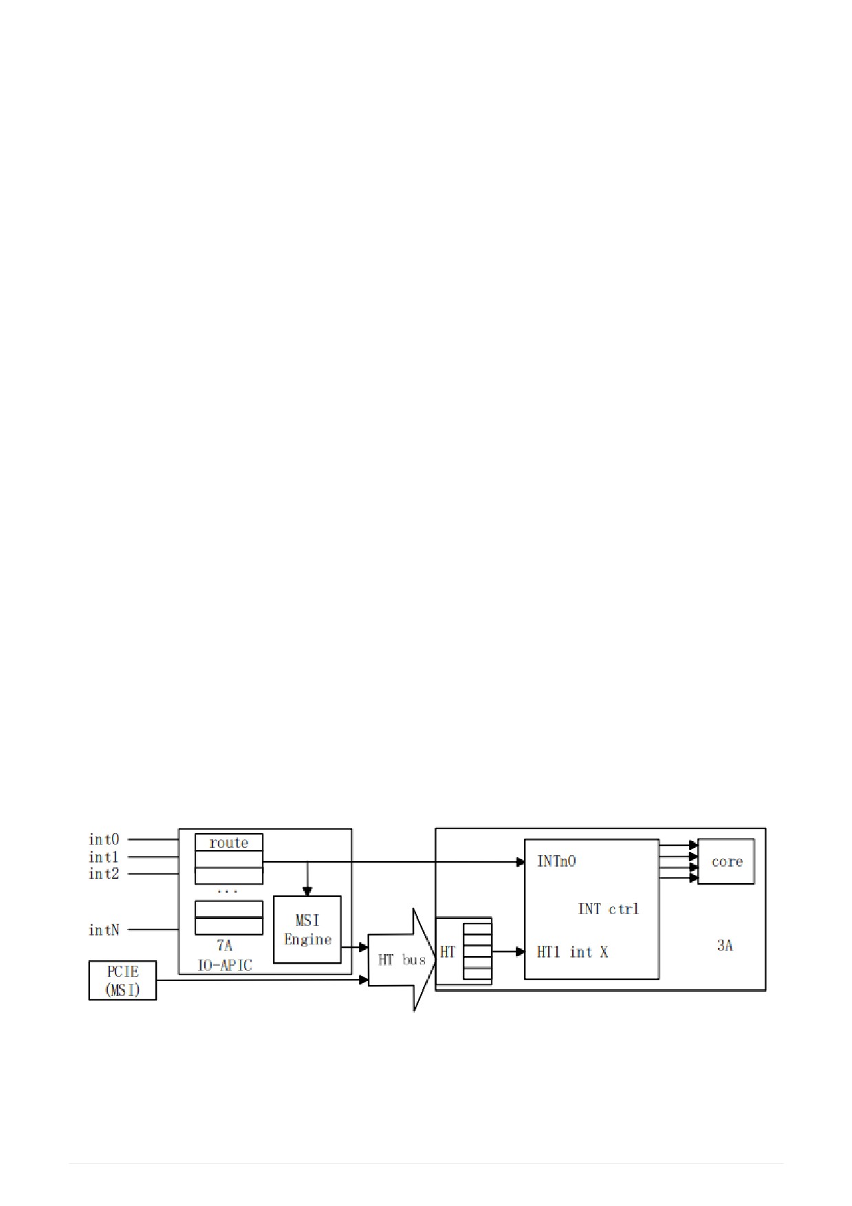
Figure 7. Schematic of the interrupt system of 3A + 7A
The figure above illustrates the hardware modules and processes involved in interrupts using the 3A+7A
computer system as an example.
The figure shows the process of the two interrupt methods, the upper part shows the interrupt through the
72
interrupt line INTn0, and the lower part shows the interrupt through the HT message packet.
The interrupt intX from the device (except for PCIE devices operating in MSI mode) is sent to the 7A
internal interrupt controller, where it is routed to the bridge pin or converted into an HT packet and sent to
the 3A’s HT controller, which receives the interrupt through the external interrupt pin or HT controller
interrupt, and is routed through the interrupt to The interrupt controller of 3A receives the interrupt through
external interrupt pin or HT controller interrupt and interrupts a processor core through interrupt route.
The address space of the bridge interrupt controller is 4KB, and the starting address (internal space of the
bridge) is configured by the BIOS.
5.1. Interrupt Source Assignment
The internal devices of the bridge chip are connected to the interrupt controller via interrupt lines. The
interrupt pin assignment of the interrupt controller is shown in the follow Table. AC97 controller and HDA
controller share one interrupt pin, GPIO0-3 share one interrupt pin, and other GPIOs share one interrupt
pin.
Table 63. Bridge chip interrupt controller interrupt source assignment
Interrupt Pins
Interrupt Source
Interrupt Pins
Interrupt Source
-
0
32
pcie_f0_0
1
-
33
pcie_f0_1
-
2
34
pcie_f0_2
-
3
35
pcie_f0_3
4
-
36
pcie_f1_0
-
5
37
pcie_f1_1
-
6
38
pcie_h_lo
7
-
39
pcie_h_hi
8
uart[3:0]
40
pcie_g0_lo
9
i2c[5:0]
41
pcie_g0_hi
10
-
42
pcie_g1_lo
11
-
43
pcie_g1_hi
12
gmac0_sbd
44
toy[0]
13
gmac0_pmt
45
toy[1]
14
gmac1_sbd
46
toy[2]
15
gmac1_pmt
47
acpi_int
16
sata[0]
48
usb_0_ehci
17
sata[1]
49
usb_0_ohci
18
sata[2]
50
usb_1_ehci
19
lpc
51
usb_1_ohci
20
-
52
rtc[0]
-
21
53
rtc[1]
73
Interrupt Pins
Interrupt Source
Interrupt Pins
Interrupt Source
22
-
54
rtc[2]
-
23
55
hpet_int
24
pwm[0]
56
ac97_dma[0]
25
pwm[1]
57
ac97_dma[1]
26
pwm[2]
58
ac97/hda
27
pwm[3]
59
gpio_hi
28
dc
60
gpio[0]
29
gpu
61
gpio[1]
30
gmem
62
gpio[2]
31
thsens
63
gpio[3]
5.2. Description of Interrupt-related Registers
The bridge chip’s interrupt controller has a set of control and status registers for each interrupt source.
Table 64. Interrupt control and status registers
Register Name
Length
Read/Writ
Description
Default
e
Value
INT_MASK
1
R/W
Interrupt Mask Register.
1
0: Enable the interrupt.
1: Mask this interrupt.
R/W
HTMSI_EN
1
HT packet interrupt enable register.
0
0: Turn off the HT message packet mode.
1: Enable the HT message packet mode.
R/W
Trigger mode setting register.
INTEDGE
1
0
0: Level-triggered interrupt.
1: Edge-triggered interrupt.
INTCLR
1
WO
Edge-triggered interrupt clear register.
N/A
Write 1 clears the interrupt, write 0 has no
effect.
74
Register Name
Length
Read/Writ
Description
Default
e
Value
R/W
Interrupt distribution mode control register
AUTO_CTRL0
1
0
(used in conjunction with AUTO_CTRL1).
{AUTO_CTRL1, AUTO_CTRL0}.
00b: fixed distribution mode.
01b: rotating distribution mode.
10b: idle distribution mode.
11b: Busy distribution mode.
AUTO_CTRL1
1
R/W
Interrupt distribution mode control register
0
(used in conjunction with AUTO_CTRL0).
{AUTO_CTRL1, AUTO_CTRL0}.
00b: fixed distribution mode.
01b: rotating distribution mode.
10b: idle distribution mode.
11b: Busy distribution mode.
ROUTE_ENTRY
8
R/W
Interrupt Routing Register.
01b
Used to configure which processor to route
this interrupt to. This register is organized in
the form of a bitmap.
Bit0: Routed to INTn0/HT controller lo; bit1:
Routed to INTn1/HT controller hi. bit7:2:
Reserved.
R/W
HT message packet interrupt vector register.
See below
HTMSI_VECTOR
8
INTISR_CHIP0
1
RO
Routing to the interrupt status (in service)
0
register of INTn0.
0: no interrupts.
1: with interrupts.
RO
Routing to INTn1’s interrupt status (in service)
INTISR_CHIP1
1
0
register.
0: no interrupts.
1: with interrupts.
75
Register Name
Length
Read/Writ
Description
Default
e
Value
RO
Interrupt request register.
INTIRR
1
0
0: no interrupt request.
1: Interrupt request is available.
INTISR
1
RO
Interrupt status (in service) register.
0
0: no interrupt is being received.
1: There are interrupts being received.
R/W
Interrupt level trigger polarity selection
INT_POLARITY
1
0
register. For the level trigger type.
0: High level trigger.
1: Low level trigger.
The address distribution of the registers related to the interrupt controller is shown in the following table
Interrupt register address distribution
Table 65. Interrupt register address distribution
Register Name
Address
Read/Write
Description
Offset
INT_ID
0x000
RO
Interrupt controller identification register
R/W
Interrupt Mask Register
INT_MASK
0x020
R/W
HT message packet interrupt enable register
HTMSI_EN
0x040
INTEDGE
0x060
R/W
Trigger mode setting register
WO
Edge-triggered interrupt clear register
INTCLR
0x080
R/W
Interrupt distribution mode control register 0
AUTO_CTRL0
0x0c0
AUTO_CTRL1
0x0e0
R/W
Interrupt distribution mode control register 1
R/W
Interrupt routing register [ 7- 0]
ROUTE_ENTRY_0
0x100
R/W
Interrupt routing register [15- 8]
ROUTE_ENTRY_8
0x108
ROUTE_ENTRY_16
0x110
R/W
Interrupt Routing Register [23-16]
R/W
Interrupt Routing Register [31-24]
ROUTE_ENTRY_24
0x118
R/W
Interrupt routing register [39-32]
ROUTE_ENTRY_32
0x120
ROUTE_ENTRY_40
0x128
R/W
Interrupt Routing Register [47-40]
R/W
Interrupt Routing Register [55-48]
ROUTE_ENTRY_48
0x130
R/W
Interrupt Routing Register [63-56]
ROUTE_ENTRY_56
0x138
HTMSI_VECTOR0
0x200
R/W
HT Interrupt Vector Register [ 7- 0]
R/W
HT Interrupt Vector Register [15- 8]
HTMSI_VECTOR8
0x208
76
Register Name
Address
Read/Write
Description
Offset
R/W
HT Interrupt Vector Register [23-16]
HTMSI_VECTOR16
0x210
HTMSI_VECTOR24
0x218
R/W
HT Interrupt Vector Register [31-24]
R/W
HT Interrupt Vector Register [39-32]
HTMSI_VECTOR32
0x220
R/W
HT Interrupt Vector Register [47-40]
HTMSI_VECTOR40
0x228
HTMSI_VECTOR48
0x230
R/W
HT Interrupt Vector Register [55-48]
R/W
HT Interrupt Vector Register [63-56]
HTMSI_VECTOR56
0x238
RO
Interrupt status (in service) register routed to
INTISR_0
0x300
INTn0
RO
Interrupt status (in service) register routed to
INTISR_1
0x320
INTn1
RO
Interrupt request register
INTIRR
0x380
INTISR
0x3a0
RO
Interrupt Status (In Service) Register
R/W
Interrupt trigger level selection register
INT_POLARITY
0x3e0
Interrupt controller identification register
Address Offset: 000-003h
Attribute: RO
Default value: 07000000h Size: 32 bits
Table 66. Interrupt controller identification register 1
Bit Field
Name
Read/Write
Description
RO
Interrupt Controller ID
31:24
id
23:0
Reserved
RO
Reserved
Address Offset: 004-007h
Attribute: RO
Default value: 003F0001h
Size: 32 bits
Table 67. Interrupt controller identification register 2
Bit Field
Name
Read/Write
Description
RO
Reserved
31:24
Reserved
23:16
int_num
RO
The number of interrupt sources supported. The
actual number of interrupts is equal to the value of
this field plus 1.
RO
Reserved
15:8
Reserved
77
Bit Field
Name
Read/Write
Description
7:0
version
RO
Interrupt controller version number
Interrupt mask register
Address Offset: 020-023h
Attribute: R/W
Default value: FFFFFFFFh
Size: 32 bits
Table 68. Interrupt mask register 1
Bit Field
Name
Read/Write
Description
31:0
int_mask
R/W
Low 32 bits of the interrupt mask register (bit[31:0])
Address Offset: 024-027h
Default value: FFFFFFFFh
Attribute: R/W
Size: 32 bits
Table 69. Interrupt mask register 2
Bit Field
Name
Read/Write
Description
31:0
int_mask
R/W
High 32 bits of the interrupt mask register
(bit[63:32])
HT interrupt message packet enable register
Address Offset: 040-043h
Default value: 00000000h
Attribute: R/W
Size: 32 bits
Table 70. HT interrupt message packet enable register 1
Bit Field
Name
Read/Write
Description
31:0
htmsi_en
R/W
Low 32 bits (bit[31:0]) of the HT Interrupt Message
Packet Enable Register
Address Offset: 044-047h
Default value: 00000000h
Attribute: R/W
Size: 32 bits
78
Table 71. HT interrupt message packet enable register 2
Bit Field
Name
Read/Write
Description
31:0
htmsi_en
R/W
High 32 bits (bit[63:32]) of the HT Interrupt Message
Packet Enable Register
Interrupt trigger control register
Address Offset: 060-063h
Attribute: R/W
Default value: 00000000h
Size: 32 bits
Table 72. Interrupt trigger control register 1
Bit Field
Name
Read/Write
Description
31:0
int_edge
R/W
Low 32 bits of the interrupt trigger control register
(bit[31:0])
Address Offset: 064-067h
Attribute: R/W
Default value: 00000000h
Size: 32 bits
Table 73. Interrupt trigger control register 2
Bit Field
Name
Read/Write
Description
R/W
High 32 bits of the interrupt trigger control register
31:0
int_edge
(bit[63:32])
Interrupt clear register
Address Offset: 080-083h
Attribute: WO
Default value: N/A
Size: 32 bits
Table 74. Interrupt clear register 1
Bit Field
Name
Read/Write
Description
31:0
int_clear
WO
Low 32 bits of the interrupt clear register (bit`[31:0]`)
Address Offset: 084-087h
Attribute: WO
Default value: 00000000h
79
Size: 32 bits
Table 75. Interrupt clear register 2
Bit Field
Name
Read/Write
Description
31:0
int_clear
WO
High 32 bits of the interrupt clear register
(bit`[63:32]`)
INT_AUTO_CTRL0 register
Address Offset: 0C0-0C3h
Attribute: R/W
Default value: 00000000h
Size: 32 bits
Table 76. INT_AUTO_CTRL0 register 1
Bit Field
Name
Read/Write
Description
31:0
int_auto_ctrl0
R/W
Low 32 bits (bit`[31:0]) of Interrupt Smart
Distribution Control Register `0
Address Offset: 0C4-0C7h
Default value: 00000000h
Attribute: R/W
Size: 32 bits
Table 77. INT_AUTO_CTRL0 register 2
Bit Field
Name
Read/Write
Description
31:0
int_auto_ctrl0
R/W
High 32 bits (bit`[63:32]) of Interrupt Smart
Distribution Control Register `0
INT_AUTO_CTRL1 register
Address Offset: 0E0-0E3h
Default value: 00000000h
Attribute: R/W
Size: 32 bits
Table 78. INT_AUTO_CTRL1 register 1
Bit Field
Name
Read/Write
Description
R/W
31:0
int_auto_ctrl1
Low 32 bits (bit[31:0]) of Interrupt Smart Distribution
Control Register 1
Address Offset: 0E4-0E7h
80
Default value: 00000000h
Attribute: R/W
Size: 32 bits
Table 79. INT_AUTO_CTRL1 register 2
Bit Field
Name
Read/Write
Description
31:0
int_auto_ctrl1
R/W
High 32 bits (bit`[63:32]) of Interrupt Smart
Distribution Control Register `1
Interrupt routing configuration register
Address Offset: 100-103h
Attribute: R/W
Default value: 01010101h
Size: 32 bits
Table 80. Interrupt routing configuration register 1
Bit Field
Name
Read/Write
Description
31:0
Reserved
R/W
Reserved
Address Offset: 104-107h
Default value: 01010101h
Attribute: R/W
Size: 32 bits
Table 81. Interrupt routing configuration register 2
Bit Field
Name
Read/Write
Description
R/W
Reserved
31:0
Reserved
Address Offset: 108-10Bh
Default value: 01010101h
Attribute: R/W
Size: 32 bits
Table 82. Interrupt routing configuration register 3
Bit Field
Name
Read/Write
Description
R/W
Reserved
31:16
Reserved
9:8
i2c_int_route
R/W
I2C Interrupt Routing Configuration Register
1:0
uart_int_route
R/W
UART Interrupt Routing Configuration Register
81
Address Offset: 10C-10Fh
Attribute: R/W
Default value: 01010101h
Size: 32 bits
Table 83. Interrupt routing configuration register 4
Bit Field
Name
Read/Write
Description
25:24
gmac1_pmt_int_route
R/W
GMAC1_PMT Interrupt Routing Configuration
Register
R/W
17:16
gmac1_sbd_int_route
GMAC1_SBD Interrupt Routing Configuration
Register
R/W
9:8
gmac0_pmt_int_route
GMAC0_PMT Interrupt Routing Configuration
Register
1:0
gmac0_sbd_int_route
R/W
GMAC0_SBD Interrupt Routing Configuration
Register
Address Offset: 110-113h
Attribute: R/W
Default value: 01010101h
Size: 32 bits
Table 84. Interrupt routing configuration register 5
Bit Field
Name
Read/Write
Description
R/W
25:24
lpc_int_route
LPC Interrupt Routing Configuration Register
R/W
17:16
SATA2_int_route
SATA2 Interrupt Routing Configuration Register
R/W
9:8
SATA1_int_route
SATA1 Interrupt Routing Configuration Register
1:0
SATA0_int_route
R/W
SATA0 Interrupt Routing Configuration Register
Address Offset: 114-117h
Attribute: R/W
Default value: 01010101h
Size: 32 bits
Table 85. Interrupt routing configuration register 6
Bit Field
Name
Read/Write
Description
31:0
Reserved
R/W
Reserved
Address Offset: 118-11Bh
Attribute: R/W
82
Default value: 01010101h
Size: 32 bits
Table 86. Interrupt routing configuration register 7
Bit Field
Name
Read/Write
Description
R/W
PWM3 Interrupt Routing Configuration Register
25:24
pwm3_int_route
17:16
pwm2_int_route
R/W
PWM2 Interrupt Routing Configuration Register
R/W
PWM1 Interrupt Routing Configuration Register
9:8
pwm1_int_route
R/W
PWM0 Interrupt Routing Configuration Register
1:0
pwm0_int_route
Address Offset: 11C-11Fh
Attribute: R/W
Default value: 01010101h
Size: 32 bits
Table 87. Interrupt routing configuration register 8
Bit Field
Name
Read/Write
Description
25:24
thsens_int_route
R/W
Thsensor Interrupt Routing Configuration Register
R/W
GPU Interrupt Routing Configuration Register
17:16
gpu_int_route
R/W
GMEM Interrupt Routing Configuration Register
9:8
gmem_int_route
1:0
dc_int_route
R/W
DC Interrupt Routing Configuration Register
Address Offset: 120-123h
Attribute: R/W
Default value: 01010101h
Size: 32 bits
Table 88. Interrupt routing configuration register 9
Bit Field
Name
Read/Write
Description
R/W
PCIE_F0 Controller 3 Interrupt Routing Configuration
25:24
pcie_f0_p3_int_rout
Register
e
17:16
pcie_f0_p2_int_rout
R/W
PCIE_F0 Controller 2 Interrupt Routing Configuration
Register
e
R/W
PCIE_F0 Controller 1 Interrupt Routing Configuration
9:8
pcie_f0_p1_int_rout
Register
e
1:0
pcie_f0_p0_int_rout
R/W
PCIE_F0 Controller 0 Interrupt Routing Configuration
Register
e
Address Offset: 124-127h
83
Attribute: R/W
Default value: 01010101h
Size: 32 bits
Table 89. Interrupt routing configuration register 10
Bit Field
Name
Read/Write
Description
25:24
pcie_h_p1_int_route
R/W
PCIE_H Controller 1 Interrupt Routing Configuration
Register
17:16
pcie_h_p0_int_route
R/W
PCIE_H Controller 0 Interrupt Routing Configuration
Register
R/W
9:8
pcie_f1_p1_int_rout
PCIE_F1 Controller 1 Interrupt Routing Configuration
e
Register
1:0
pcie_f1_p0_int_rout
R/W
PCIE_F1 Controller 0 Interrupt Routing Configuration
Register
e
Address Offset: 128-12Bh
Attribute: R/W
Default value: 01010101h
Size: 32 bits
Table 90. Interrupt routing configuration register 11
Bit Field
Name
Read/Write
Description
R/W
25:24
pcie_g1_p1_int_rout
PCIE_G1 Controller 1 Interrupt Routing
e
Configuration Register
R/W
17:16
pcie_g1_p0_int_rout
PCIE_G1 Controller 0 Interrupt Routing
e
Configuration Register
9:8
pcie_g0_p1_int_rout
R/W
PCIE_G0 Controller 1 Interrupt Routing
Configuration Register
e
R/W
1:0
pcie_g0_p0_int_rout
PCIE_G0 Controller 0 Interrupt Routing
e
Configuration Register
Address Offset: 12C-12Fh
Attribute: R/W
Default value: 01010101h
Size: 32 bits
Table 91. Interrupt routing configuration register 12
Bit Field
Name
Read/Write
Description
R/W
25:24
acpi_int_route
ACPI Interrupt Routing Configuration Register
84
Bit Field
Name
Read/Write
Description
17:16
toy2_int_route
R/W
TOY2 Interrupt Routing Configuration Register
9:8
toy1_int_route
R/W
TOY1 Interrupt Routing Configuration Register
R/W
1:0
toy0_int_route
TOY0 Interrupt Routing Configuration Register
Address Offset: 130-133h
Attribute: R/W
Default value: 01010101h
Size: 32 bits
Table 92. Interrupt routing configuration register 13
Bit Field
Name
Read/Write
Description
R/W
25:24
usb1_ohci_int_route
USB1 OHCI Controller Interrupt Routing
Configuration Register
R/W
17:16
usb1_ehci_p2_int_ro
USB1 EHCI Controller Interrupt Routing
ute
Configuration Register
9:8
usb0_ohci_int_route
R/W
USB0 OHCI Controller Interrupt Routing
Configuration Register
R/W
1:0
usb0_ehci_int_route
USB0 EHCI Controller Interrupt Routing
Configuration Register
Address Offset: 134-137h
Attribute: R/W
Default value: 01010101h
Size: 32 bits
Table 93. Interrupt routing configuration register 14
Bit Field
Name
Read/Write
Description
25:24
hpet_int_route
R/W
HPET Interrupt Routing Configuration Register
17:16
rtc2_int_route
R/W
RTC2 Interrupt Routing Configuration Register
9:8
rtc1_int_route
R/W
RTC1 Interrupt Routing Configuration Register
R/W
1:0
rtc0_int_route
RTC0 Interrupt Routing Configuration Register
Address Offset: 138-13Bh
Attribute: R/W
Default value: 01010101h
Size: 32 bits
Table 94. Interrupt routing configuration register 15
85
Bit Field
Name
Read/Write
Description
25:24
gpio_hi_int_route
R/W
GPIO high bit (bit[56:4]) interrupt routing
configuration register
R/W
17:16
ac97/hda_int_route
AC97/HDA controller interrupt routing configuration
register
R/W
9:8
ac97_dma1_int_route
AC97 DMA1 Interrupt Routing Configuration Register
R/W
1:0
ac97_dma0_int_route
AC97 DMA0 Interrupt Routing Configuration Register
Address Offset: 13C-13Fh
Attribute: R/W
Default value: 01010101h
Size: 32 bits
Table 95. Interrupt routing configuration register 16
Bit Field
Name
Read/Write
Description
25:24
gpio3_int_route
R/W
GPIO3 Interrupt Routing Configuration Register
17:16
gpio2_int_route
R/W
GPIO2 Interrupt Routing Configuration Register
R/W
9:8
gpio1_int_route
GPIO1 Interrupt Routing Configuration Register
R/W
1:0
gpio0_int_route
GPIO0 Interrupt Routing Configuration Register
HT message packet interrupt vector configuration register
Address Offset: 200-203h
Attribute: R/W
Default value: 03020100h
Size: 32 bits
Table 96. HT message packet interrupt vector configuration register 1
Bit Field
Name
Read/Write
Description
31:0
Reserved
R/W
Reserved
Address Offset: 204-207h
Attribute: R/W
Default value: 070605040h
Size: 32 bits
Table 97. HT message packet interrupt vector configuration register 2
Bit Field
Name
Read/Write
Description
31:0
Reserved
R/W
Reserved
86
Address Offset: 208-20Bh
Attribute: R/W
Default value: 0B0A0908h
Size: 32 bits
Table 98. HT message packet interrupt vector configuration register 3
Bit Field
Name
Read/Write
Description
31:16
Reserved
R/W
Reserved
R/W
I2C HT Interrupt Vector Configuration Register
15:8
i2c_int_route
R/W
UART HT interrupt vector configuration register
7:0
uart_int_route
Address Offset: 20C-20Fh
Attribute: R/W
Default value: 0E0F0D0Ch
Size: 32 bits
Table 99. HT message packet interrupt vector configuration register 4
Bit Field
Name
Read/Write
Description
31:24
gmac1_pmt_int_route
R/W
GMAC1_PMT HT Interrupt Vector Configuration
Register
R/W
GMAC1_SBD HT Interrupt Vector Configuration
23:16
gmac1_sbd_int_route
Register
15:8
gmac0_pmt_int_route
R/W
GMAC0_PMT HT Interrupt Vector Configuration
Register
R/W
GMAC0_SBD HT Interrupt Vector Configuration
7:0
gmac0_sbd_int_route
Register
Address Offset: 210-213h
Attribute: R/W
Default value: 13121110h
Size: 32 bits
Table 100. HT message packet interrupt vector configuration register 5
Bit Field
Name
Read/Write
Description
31:24
lpc_int_route
R/W
LPC HT Interrupt Vector Configuration Register
R/W
SATA2 HT Interrupt Vector Configuration Register
23:16
SATA2_int_route
R/W
SATA1 HT Interrupt Vector Configuration Register
15:8
SATA1_int_route
7:0
SATA0_int_route
R/W
SATA0 HT Interrupt Vector Configuration Register
Address Offset: 214-217h
87