Loongson 3A3000/3B3000 processor user manual. Part ii GS464E processor core V1.2 - page 7
龙芯 3A3000/3B3000 处理器用户手册 y 下册
uncertain when configured as 0.
PTW
11.. 6
Page table entry table index bit width. 0 is meaningless and the processor result is
R/W
0 x0
uncertain when configured as 0.
Page table item bit width. Used to control the access page table entry index to move 3 bits
to the left (machine default data path width is 64)
PTEW
5.. 0
R/W
0 x0
Bits) that need to be moved further left. For example, when the width of each page table entry
(single page) is 16 bytes, PTEW is hard set to 1, and accessing the page table entry index moves to
the left (3+1) bit to form the final access address.
101
龙芯 3A3000/3B3000 处理器用户手册 y 下册
7.12 Wired Register (CP0 Register 6, Select 0)
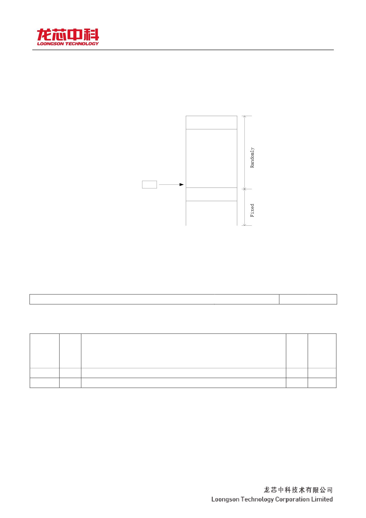
The Wired register is a read-write register that defines the boundary between fixed and random replacement
table items in VTLB. The diagram is shown in Figure 7-13.
Figure 7-13 Boundary of fixed table items and random replacement table items in VTLB
The 63th...
item
Wired register
24
The 21st...
item
Figure 7-14 illustrates the format of the Wired register; Table 7-15 describes the Wired register
fields.
Figure 7-14 Wired register format
31
6
5
0
0
Wired
Table 7-15 Description of Wired register field
Domain
posi
Functiona
Read
Reset
name
tion
l
/wri
value
descripti
te
on
0
31.. 6
Read only is always 0.
0
0
Wired
5.. 0
TLB fixes the boundary between a table entry and a random replacement table entry.
R/W
0 x0
102
龙芯 3A3000/3B3000 处理器用户手册 y 下册
7.13 PWCtl Register 6, Select 6
The PWCtl register is used in conjunction with the PWBase, PWField, and PWSize registers in GS464E to
provide configuration information for the execution of the LDDIR and LDPTE directives. The LDDIR and LDPTE
directives support traversal lookup of multilevel page table structure, which can contain up to four levels of catalog
tables and one level of page table entries. See Figure 7-9 on page 94 for the supported page table structure and
access procedure. The index value of each level page table to the next level page table or the final page table entry
is obtained by intercepting part of the contiguous bit from the virtual address to be looked up (BadVAddr). The
PWSize register is used to identify the number of contiguous bits intercepted by the page table index at each level
in the virtual address to be looked up (BadVAddr).
PWCtl controls whether the base directory table is used in page-table traversal lookup, and support for large
pages.
Figure 7-15 illustrates the format of the PWCtl register; The PWCtl register fields are described in Table 7-16.
Figure 7-15 PWCtl register format
31
30
29
7
6
5
0
0
PWDirExt
HugePg
PSn
Table 7-16 Description of the PWCtl register fields
Domain
positi
Function
Read
Reset
name
on
al
/wri
value
descript
te
ion
0
31
Read only is always 0.
0
0
PWDirExt
30
Base Directory table function enablement bit. 1: Enable; 0: Disabled.
R/W
0 x0
0
29.. 7
Read only is always 0.
0
0
HugePg
6
1 indicates that large pages are supported in the table of contents; A value of 0 indicates
R/W
0 x0
that large pages are not supported in the table of contents.
PSn
5.. 0
Used to indicate the location of the PTEVld bit of a table entry in a table of contents.
R/W
0 x0
103
龙芯 3A3000/3B3000 处理器用户手册 y 下册
7.14 Trade characters for a Register (CP0 Register 7, Select 0)
The Htrade A register holds a bit mask for controlling which hardware registers the RDHWR instruction can
read in user mode. Figure 7-16 illustrates the format of the HWRENCH a register; Tables 7-17 describe the
hWRENCH a register domains.
Figure 7-16 Trade A register format
31
30
29
28
27
26
25
24
23
22
21
20
19
18
17
16
15
14
13
12
11
10
9
8
7
6
5
4
3
2
1
0
F
S
R
Y
P
E
R
N
U
e
X
U
C
C
C
N
q
t
R
0
C
I
C
C
S
C
L
E
S
U
C
C
T
m
s
a
e
l
p
e
Table 7-17 Trade A describes the register fields
Domain
positi
Functiona
Read
Reset
name
on
l
/wri
value
descripti
te
on
FreqScale
31
RDHWR 31 enable bit. 1: Read is allowed; 0: Read disabled.
R/W
0 x0
ExtCC
30
RDHWR 30 (external Count register) enablement bit. 1: Read is allowed; 0: Read
R/W
0 x0
disabled.
ULR
29
RDHWR 29 (UserLocal register) enable bit. 1: Read is allowed; 0: Read disabled.
R/W
0 x0
0
28.. 4
Read only is always 0.
0
0
CCRes
3
RDHWR 3 (Count autoincrement) enable bit. 1: Read is allowed; 0: Read disabled.
R/W
0 x0
CC
2
RDHWR 2 (Count register) enable bit. 1: Read is allowed; 0: Read disabled.
R/W
0 x0
SYNCI -
1
RDHWR 1 (SYNCI_Step) enable bit. 1: Read is allowed; 0: Read disabled.
R/W
0 x0
Step
CPUNum
0
RDHWR 0 (EBase) enable bit. CPUNum 1: Read is allowed; 0: Read disabled.
R/W
0 x0
104
龙芯 3A3000/3B3000 处理器用户手册 y 下册
7.15 BadVAddr Register (CP0 Register 8, Select 0)
The BadVAddr register is a read-only register that records the last virtual address that caused the following
exception:
y Address Error (AdEL or AdES)
y TLB/XTLB Refill
y TLB Invalid (TLBL or TLBS)
y TLB Modified
Figure 7-17 illustrates the format of the BadVAddr register; The BadVAddr register fields are
described in Table 7-18.
Figure 7-17 BadVAddr register format
63
0
BadVAddr
Table 7-18 BadVAddr register field description
Domain
positi
Function
Read
Reset
name
on
al
/wri
value
descript
te
ion
BadVAddr
63.. 0
The wrong virtual address.
R
There is
no
105
龙芯 3A3000/3B3000 处理器用户手册 y 下册
7.16 Count Register 9, Select 0
The Count register is used in conjunction with the Compare register to implement a high-precision timer and
timed interrupts within a processor. The timer increases by 1 at 1/2 the frequency of the processor core pipeline
clock. During execution, the processor core pipeline clock frequency may be dynamically adjusted, so the self-
increasing frequency of Count changes accordingly.
The software can configure the Count register for certain functions or diagnostic purposes, such as timer reset,
synchronization, and so on. The format of the Count register is explained. The Count register fields are described.
Figure 7-18 Count register format
63
32
CountExt
31
0
The Count
Table 7-19 Count register fields are described
Domain
positio
Functional
Read
Reset
name
n
descriptio
/writ
value
n
e
CountExt
63.. 32
Internal counter high 32 bit extension.
R/W
There is no
The Count
31.. 0
Internal counter.
R/W
There is no
Programming tips:
The processor implements Count as a 64-bit counter. A timed interrupt caused by another Count/Compare
inside the processor is still triggered by comparing the low 32-bit value of Count with the value of the Compare
register. RDHWR (RD =$3) returns the result of the Count register's low 32-bit symbol being extended to 64 bits.
The MFC0 instruction can only read the result of the Count register's low 32-bit symbol extending to 64 bits, but
when the MTC0 instruction is used to write the Count register, the processor writes all the 64-bit values from the
source register to the Count register. So a recommendation: If the software wants to access the full 64-bit
information in the Count register, use the DMFC0, DMTC0 instructions.
106
龙芯 3A3000/3B3000 处理器用户手册 y 下册
7.17 GSEBase Register (CP0 Register 9, Select 6)
The GSEBase register (GSEBase register) is a read-write register (READ-write register) which is used to
prepare the base address of the loongson extension exception vector.
Figure 7-20 illustrates the format of the GSEBase register; Table 7-21 describes the GSEBase register fields.
Figure 7-19 GSEBase register format
63
32
The Exception
Base
31
12
11
10
0
The Exception
WG
0
Base
Table 7-20 Description of GSEBase register fields
Domain
positi
Functiona
Read
Reset
name
on
l
/wri
value
descripti
te
on
When status. BEV=0, the logic moves 12 bits to the left as the base
The
0 XFFFF.
address of the entry vector for the godson extension exception.
63.. 12
R/W
FFFF
Excepti
The [63:30] bit can only be written if the WG bit is equal to 1, and the EBase register if
8000.0.
on
the WG bit is equal to 0
The bit [63:30] remains the same.
Base
The [63:30] write control bit.
WG
11
1: ExceptionBase[63:30] can be written;
0:
R/W
0 x0
ExceptionBase[63:30] remained unchanged
when written.
0
10.. 0
Read only is always 0.
0
0
107
龙芯 3A3000/3B3000 处理器用户手册 y 下册
7.18 PGD Register (CP0 Register 9, Select 7)
The PGD register is a read-only register that holds the base address of the page table.
Figure 7-20 illustrates the format of the PGD register; The PGD register fields are described in Table 7-21.
Figure 7-20 PGD register format
63
0
The Page Table
Base
Table 7-21 Description of PGD register fields
Domain
positio
Functional
Read
Reset
name
n
descriptio
/writ
value
n
e
When bit 63 in BadVaddr register is 1, the value of Page Table Base is equal to the value
The
in KScratch6 register;
Page
63.. 0
R
0 x0
When bit 63 in BadVaddr register is 0, the value of Page Table Base is equal to that in
Tabl
PWBase register
e
Stored value.
Base
108
龙芯 3A3000/3B3000 处理器用户手册 y 下册
7.19 EntryHi Register (CP0 Register 10, Select 0)
The EntryHi register is used to store high-level information about TLB table entries during TLB read, write,
and query access.
Under normal instruction execution, the EntryHi domain holds the current address space id filled by the
software and participates in TLB look-up along with the virtual address of a finger or fetch operation. ASID When
a TLB exception occurs (the TLB Refill, XTLB Refill, TLB Invalid, or TLB Modifid exception), the appropriate
portion of the error address that triggered the exception is written to the EntryHi and EntryHi fields. RVPN2 When
the TLBP instruction is executed, the virtual address information and address space identification information for
the items to be looked up are stored in the EntryHi, EntryHi, and EntryHi domains for TLB lookup. RVPN2ASID
When the TLBR instruction is executed, reading from the specified TLB table entry is also written to the
corresponding field of the EntryHi register. Because the EXECUTION of the TLBR instruction overwrites the
EntryHi domain, the software must save the ASID domain value before executing the TLBR instruction and
recover in time after the TLBR execution. ASID This is particularly important for the TLB Invalid and TLB
Modified exception handler, and other associated memory management code.
When the TLBWI and TLBWR directives are executed, the virtual address information and address space
identification information for the entry to be written are stored in the EntryHi, EntryHi, and EntryHi fields for the
TLB write. RVPN2ASID If you set the EntryHi field to 1 when executing the TLBWI instruction, you can
invalidate the specified TLB table entry. EHINV Since the EntryHi domain is also overwritten by the CONTENTS
of the TLBR instruction readout, it is important to maintain the EHINV domain as well as the ASID domain when
executing the TLBR instruction, which is important for subsequent TLBWI instructions to execute correctly.
EHINV
Figure 7-21 illustrates the format of the EntryHi register; Table 7-22 describes the EntryHi register fields.
Figure 7-21 In the EntryHi register format
63
62
61
48
47
32
R
0
VPN2
31
13
12
11
10
9
8
7
0
EH
VPN2
0
0
ASID
INV
Table 7-22 Description of the EntryHi register field
Domain
positi
Functiona
Read
Reset
name
on
l
/wri
value
descripti
te
on
109
龙芯 3A3000/3B3000 处理器用户手册 y 下册
An area identifies a bit, corresponding to the [63:62] bit of
the virtual address.
0B00: User address region
R
63.. 62
(XUSeg, User Address region);
0B01: Supervisor
R/W
0 x0
Address Region (XSSEG, Supervisor Address Region);
0B10: Retention;
0B11: Kernel address region (Xkseg, Kernel Address region).
0
61.. 48
Read only is always 0.
0
0
VPN2
47.. 13
The virtual page number is divided by 2(mapped to a double page) and corresponds to the
R/W
0 x0
[47:13] bit of the virtual address.
0
12.. 11
Read only is always 0.
0
0
TLB invalid token bit.
EHINV 1
10
When the position is 1, executing the TLBWI instruction invalidates the corresponding
R/W
0 x0
TLB table entry.
When the TLBR instruction is executed, the bit is set to 1 if the TLB table entry read is
invalid.
0
9.. 8
Read only is always 0.
0
0
1 although Config4=0, GS464E still implements the EHINV domain according to the definition of MIPS specification in the case of Config4>1.
IEIE It is recommended to use the
EntryHi domain functionality for software such as the GS464E deeply customized kernel to facilitate TLB
management. EHINV
110
龙芯 3A3000/3B3000 处理器用户手册 y 下册
Domain
positi
Functiona
Read
Reset
name
on
l
/wri
value
descripti
te
on
Address space identification number. Used to share TLB between multiple processes; By
ASID
7.. 0
R/W
0 x0
using the ASID to differentiate, for the same
Virtual page number, which allows different processes to take different mappings.
105
龙芯 3A3000/3B3000 处理器用户手册 y 下册
7.20 Compare Register (CP0 Register 11, Select 0)
The Compare register is combined with the Count register to implement a high-precision timer and timed
interrupts inside a processor. The value stored in the Compare register remains unchanged after writing, compared
to the low 32-bit Count register, and when both are equal, the timer is interrupted, causing the Cause to be 1. IT
When vector interrupt mode is not in use, timer interrupt will connect to the break 7 (Cause, hard break 5). IP7
When using vector interrupt mode, the interrupt line to which the timer interrupts is determined by IntCtl. IPTI
When the software writes the Compare register, the hardware automatically clears the Cause of 0, thus
clearing the timer interrupt. IT
Figure 7-22 illustrates the format of the Compare register; Table 7-23 describes the Compare register fields.
Figure 7-22 Compare register format
31
0
The Compare
Table 7-23 Compare register field description
Domain
positi
Functiona
Read
Reset
name
on
l
/wri
value
descripti
te
on
The
31.. 0
Interval counts compare values.
R/W
0 x0
Compare
106
龙芯 3A3000/3B3000 处理器用户手册 y 下册
7.21 Status Register (CP0 Register 12, Select 0)
The Status register is a read-write register that contains processor mode of operation, interrupt enablement,
and processor Status diagnostics. Figure 7-23 illustrates the Status register format; Table 7-24 describes the Status
register fields.
Figure 7-23 Status register format
31
30
29
28
27
26
25
24
23
22
21
20
19
18
17
16
15
14
13
12
11
10
9
8
7
6
5
4
3
2
1
0
0
CU2CU1CU0 Th
FR
0
MX
PX
BEV 0
Th
NMI 0
MID
IM7..
KX SX
UX KSU
ERLEXL IE
e
e
IM0
RP
SR
Table 7-24 Description of the Status register fields
Domain
positi
Functiona
Read
Reset
name
on
l
/wri
value
descripti
te
on
0
31
Read only is always 0.
0
0
CU2
30
Coprocessor 2 has identity bits available. 1: Available; 0: Disabled.
R/W
0 x0
CU1
29
Coprocessor 1(floating point coprocessor) can be used to identify bits. 1: Available; 0:
R/W
0 x1
Disabled.
The coprocessor 0 is available with identity bits. 1: Available; 0: Disabled.
CU0
28
When the processor is in Kernel mode and Debug mode, coprocessor 0 can always be
R/W
0 x1
used without consideration
CU0 bit is equal to 1.
The RP
27
Processor dynamic frequency down enable bit. 1: Open; 0: Off.
R/W
0 x0
The floating point register mode controls the bits.
FP
26
0:16 floating-point registers, even numbered, each 64-bit, single-precision stored on the
R/W
0 x0
lower 32-bit;
1:32 floating point registers, serial Numbers, each 64-bit, single-precision stored in low
32-bit.
0
25
Read only is always 0.
0
0
MX
24
Enable bits to access DSP resources. 1: Accessible; 0: No access.
R/W
0 x0
Enable control bits for 64-bit operations in user mode are not used to enable the 64-bit address
space. (The rest of the mode
PX.
23
R/W
0 x1
64-bit operation without enabling)
1: Enabling; 0: Disabled.
BEV
22
Exception vector entry address control. 0: Normal; 1: Boot up.
R/W
0 x1
0
21
Read only is always 0.
0
0
Used to indicate that the entry leading to the Reset exception vector is
due to Soft Reset. 1: Soft reset; 0: Not a soft Reset (possibly NMI or
The SR
20
R/W
0 x0
Reset).
The jump.
107
龙芯 3A3000/3B3000 处理器用户手册 y 下册
Used to indicate that the reset exception vector entry is due to a non-masking interrupt
(NMIt).
NMI
19
R/W
0 x0
1: It is non-masking interrupt; 0: It is not a non-masking interrupt (Reset or Soft Reset).
The jump.
0
18
Read only is always 0.
0
0
108
龙芯 3A3000/3B3000 处理器用户手册 y 下册
Domain
positi
Functiona
Read
Reset
name
on
l
/wri
value
descripti
te
on
The loong-son custom field is used to indicate which address space the current default operation
is in. Whether the address space in which the reference falls is controlled by the MID domain is
determined by the diag.inst domain. If a visit memory operation does not carry MID
information, it will fall in the address space specified in the root.status.mid field; otherwise, it
MID
17.. 16
R/W
0 x0
will fall in the address space determined by the MID information carried by it.
GS464E USES a 2-bit code (MID) to identify the four isolated full address Spaces.
MID=0 is the address space visible to MIPS host, MID=1 is the address space visible to
virtual machines in guest mode, and other values of MID can be assigned to other virtual
machines by software.
The MID field can be written only when dig.vmm =1, and will be set to 0 no matter what
value is written when dig.vmm =0.
Interrupt mask bit. Each bit controls the enabling of an external interrupt, an internal
IM7.. IM0
15.. 8
R/W
0 x0
interrupt, or a software interrupt.
1: Enabling; 0: Masking.
1. Can access 64-bit Kernel segment, which USES XTLB Refill exception vector;
KX
7
R/W
0 x1
0:64-bit Kernel segment cannot be accessed. Kernel segment access USES the
EXCEPTION vector TLB Refill.
1. Can access the 64-bit Supervisor segment, which USES the XTLB Refill exception
SX
6
R/W
0 x1
vector;
0: The 64-bit Supervisor segment cannot be accessed. The Supervisor segment accesses
use the TLB Refill exception vector.
1: Can access 64-bit User segment, which USES XTLB Refill exception vector and allows instruction
operation of 64-bit data in User mode;
UX
5
R/W
0 x1
0:64-bit User segment cannot be accessed. User segment access USES the TLB Refill
exception vector and does not allow User modules
The following instruction operates on 64-bit data.
Processor mode identifies bits.
0B00: Kernel Mode 0B01:
KSU
4.. 3
Supervisor Mode 0B10: User
R/W
0 x0
Mode
0B11: Reserve.
Error level. This bit is set to 1 when Reset, Soft Reset, NMI, and Cache Error
exceptions occur. 0: Normal; 1: Error level.
When ERL position is 1:
ERL
2
y The processor is automatically in core mode
R/W
0 x1
y All hardware and software interrupts are shielded
y The ERET instruction reads the return address from the ErrorEPC register
y Kuseg segments will be treated as having directly mapped non-cached attributes
(Unmapped and uncached)
108
龙芯 3A3000/3B3000 处理器用户手册 y 下册
The exception class. This bit is set to 1 when an exception occurs that is not Reset, Soft
Reset, NMI, or Cache Error exceptions. 0: Normal; 1: Exception level.
When position 1 of EXL is:
y The processor is automatically in core mode
EXL
1
R/W
0 x0
y All hardware and software interrupts are shielded
y TLB/XTLB Refill exception processing adopts general exception vector entry
instead of TLB/XTLB Refill exception vector entry
y EPC, Cause do not update when new exceptions occur. BD
Global interrupt enablement bit.
IE
0
0: Screen all hardware and software interrupts;
R/W
0 x0
1: Enable all hardware and software interrupts.
109
龙芯 3A3000/3B3000 处理器用户手册 y 下册
7.22 IntCtl Register (CP0 Register 12, Select 1)
The IntCtl register is a read-write register that extends the interrupt mechanism of the processor.
Figure 7-24 illustrates the format of the IntCtl register; The IntCtl register fields are described in Table 7-25.
Figure 7-24 IntCtl register format
31
29
28
26
25
10
9
5
4
0
IPTI
IPPCI
0
VS
0
Table 7-25 IntCtl register fields are described
Domain
positi
Functiona
Read
Reset
name
on
l
/wri
value
descripti
te
on
Used in vector interrupt mode to indicate on which interrupt line the timer interrupt
IPTI
31.. 29
R
0 x7
merges.
The value is constant 7, indicating that it is merged in IP7, and the hardware is
disconnected on HW5.
Used in vector interrupt mode to indicate on which interrupt line the performance counter
IPPCI
28.. 26
R
0 x7
overflows the interrupt.
The value is constant 7, indicating that it is merged in IP7, and the hardware is
disconnected on HW5.
0
25.. 10
Read only is always 0.
0
0
Used to define the space between interrupt vector entry addresses in vector interrupt
mode.
VS
Vector space
coding
0 x00
0 x000
VS.
9.. 5
R/W
0 x0
0 x01
0 x020
0 x02
0 x040
0 x04
0 x080
0 x08
0 x100
The encoding values are retained except for those listed in the table above. If a reserved
0 x10
0 x200
value is configured for the VS domain, processor results will be indeterminate.
0
4.. 0
Read only is always 0.
0
0
109
龙芯 3A3000/3B3000 处理器用户手册 y 下册
7.23 SRSCtl Register (CP0 Register 12, Select 2)
The SRSCtl register is used to control the shadow register. Since GS464E implements only one set of general
purpose registers, the shadow of the general purpose register is the general purpose register itself.
Figure 7-25 illustrates the format of the SRSCtl register; The SRSCtl register fields are described in Table 7-
26.
Figure 7-25 SRSCtl register format
31
30
29
26
25
16
15
12
11
10
9
6
5
4
3
0
0
HSS
0
ESS
0
PSS
0
CSS
Table 7-26 SRSCtl register field description
Domain
positi
Functiona
Read
Reset
name
on
l
/wri
value
descripti
te
on
0
31.. 30
Read only is always 0.
0
0
HSS
29.. 26
A value of 0 indicates that only one set of general purpose registers is implemented.
R
0 x0
0
25.. 16
Read only is always 0.
0
0
The group number of the shadow register group used for exception handling. GS464E can
ESS
15.. 12
R/W
0 x0
only write 0 and other value handler rows
Is uncertain.
0
11.. 10
Read only is always 0.
0
0
PSS
9.. 6
The group number of the previous set of shadow registers. GS464E can only write 0,
R/W
0 x0
write other values processor behavior is uncertain.
0
5.. 4
Read only is always 0.
0
0
CSS
3.. 0
The value is always 0, indicating that the current shadow register group is the general
R
0 x0
purpose register group.
110
龙芯 3A3000/3B3000 处理器用户手册 y 下册
7.24 Cause Register (CP0 Register 13, Select 0)
The Cause register is used primarily to describe the Cause of the most recent exception. In addition, software
interrupt and interrupt vector are also controlled. In addition to
IP1.. Outside the DC, IV and WP domains, the other domains of the Cause register are read-only to the
software.
Figure 7-26 illustrates the format of the Cause register; Table 7-27 describes the Cause register fields.
Figure 7-26 Cause register format
31
30
29
28
27
26
25
24
23
22
21
20
19
18
17
16
15
14
13
12
11
10
9
8
7
6
5
4
3
2
1
0
BD
TI
CE
DC
PCI
0
IV
0
IP7 IP6 IP5 IP4 IP3 IP2 IP1 IP0
0
ExcCode
Table 7-27 Description of the Cause register field
Domain
positi
Functiona
Read
Reset
name
on
l
/wri
value
descripti
te
on
BD
31
Identifies whether the instruction with the most recent exception is in the branch delay
R
0 x0
slot.
1: In the delay slot; 0: Not in the delay slot
TI
30
Timer interruption indication. 1: Interruption of timer to be handled; 0: No timer
R
0 x0
interrupt.
CE
29.. 28
Records the coprocessor number that is unavailable when an exception occurs.
R
0 x0
DC
27
The Count register disables the Count control bit. 1: Stop the Count; 0: Enable Count
R/W
0 x0
Count.
Performance counter overflow interrupt indication.
PCI
26
R
0 x0
1: Performance counter overflow interrupt to be processed; 0: No performance counter
overflow interrupt.
0
25.. 24
Read only is always 0.
0
0
Interrupt exception vector entry control bit.
IV
23
R/W
0 x0
1: Special interrupt vector (0x200) is used; 0: Use the generic exception vector (0x180).
0
22.. 16
Read only is always 0.
0
0
Pending hardware interrupt identification. Each bit corresponds to a middle break, and
IP7.. IP2
15.. 10
R
0 x0
IP7~IP2 correspond to hardware interrupt 5~0 in turn.
1: The interrupt to be processed on the interrupt line; 0: There is no interrupt on the
interrupt line.
Pending software interrupt identification. Each bit corresponds to a software interrupt, and
IP1.. IP0
9.. 8
R/W
0 x0
IP1~IP0 corresponds to software interrupt 1~0 in turn.
The software interrupt identification bit can be set and cleared by the software.
0
7
Read only is always 0.
0
0
ExcCode
6.. 2
Exception coding. Please see the detailed description.
0
1.. 0
Read only is always 0.
0
0
Table 7-28 ExcCode codes and their corresponding exception types
111
龙芯 3A3000/3B3000 处理器用户手册 y 下册
ExcCode
mnemoni
desc
cs
ribe
0 x00
Int
interrupt
0 x01
The Mod
TLB modification exceptions
0 x02
TLBL
TLB exception (read data or fetch instruction)
0 x03
TLBS
TLB exception (write data)
0 x04
AdEL
Address error exception (read data or fetch instruction)
0 x05
AdES
Address error exception (write data)
112
龙芯 3A3000/3B3000 处理器用户手册 y 下册
ExcCode
mnemonics
desc
ribe
MIPS specifies a defined bus error exception (fetch instruction). Because GS464E does
0 x06
IBE
not implement the IBE exception, the reason for the exception is retained in the encoding.
If the system prints "Bus Error" in the software debugging, please focus on checking
whether there are other exceptions.
Bus error exception (read or write data). Because GS464E does not implement the DBE
0 x07
DBE
exception, the reason for the exception is encoded.
If the system prints "Bus Error" in the software debugging, please focus on checking
whether there are other exceptions.
0 x08
Sys
The system call exception.
Break point exception.
0 x09
Bp
If SDBBP instructions are executed in EJTAG Debug mode, the exception encoding
0x9(Bp) is written to Debug
Register in the DExcCode field.
0 x0a
RI
Preserve instruction exceptions.
0 x0b
The CpU
No exceptions can be made to the coprocessor.
0 x0c
Ov
Calculate the overflow exception.
0 x0d
The Tr
Trap exception.
0 x0e
MSAFPE
Unrealized.
0 x0f
FPE
The floating point exception.
Loongson custom exception. Includes floating point stack exception, virtual machine
0 x10
GSExc
memory management exception, virtual machine space TLB example
Outside. The software can look at the related fields of the GSCause register to see
exactly what exceptions occur.
0 x11
-
reserve
0 x12
-
reserve
0 x13
TLBRI
TLB reads prevent exceptions
0 x14
TLBXI
TLB performs blocking exceptions
0 x15
MSADis
Unrealized.
0 x16
MDMX
Unrealized.
0 x17
WATCH
Unrealized.
0 x18
MCheck
Unrealized.
0 x19
The Thread
Unrealized.
0 x1a
DSPDis
The DSP module disables exceptions
0 x1b
GE
Unrealized.
0 x1c
-
reserve
0 x1d
-
reserve
Cache error exception.
Because the Cache error exception USES a dedicated vector entry address, the Cause register's
0 x1e
-
ExcCode field is not updated when the Cache error exception occurs in normal mode. When in Debug
mode, the exception encoding 0x1e is written to the DExcCode field of the Debug register.
0 x1f
-
reserve
112
龙芯 3A3000/3B3000 处理器用户手册 y 下册
7.25 EPC Register (CP0 Register 14, Select 0)
The EPC register is a 64-bit read-write register that contains a PC that continues to execute instructions after
the exception processing has completed. In response to the synchronous (exact) exception, the processor writes to
the EPC register:
The PC directly triggers the exception instruction.
When the instruction that directly triggered the exception is in the branch delay slot, record the PC of the
previous branch or jump instruction of the instruction, at the same time caus.bd
Set to 1.
In response to an asynchronous (imprecise) exception, a PC in which the processor writes an instruction to the
EPC register that continues execution after the exception processing has completed. The EPC register is not
updated when the Status register EXL bit is 1.
The format of EPC register is explained. The EPC register fields are described.
Figure 7-27 EPC register format
63
0
The EPC
Table 7-29 Description of EPC register fields
Domain
positi
Functiona
Read
Reset
name
on
l
/wri
value
descripti
te
on
The EPC
63.. 0
Exception program counter.
R/W
There is
no
113
龙芯 3A3000/3B3000 处理器用户手册 y 下册
7.26 PRId Register (CP0 Register 15, Select 0)
The PRId register is a 32-bit read-only register that contains information identifying the MIPS processor
manufacturer, processor type, and implementation version.
Figure 7-28 illustrates the format of the PRId register; The PRId register fields are described in Table 7-30.
Figure 7-28 PRId register format
31
24
23
16
15
8
7
0
0
CompanyID
Processor ID
Revision
Table 7-30 Description of the PRId register fields
Domain
position
Function
Read
Reset
name
al
/wri
value
descript
te
ion
0
31.. 24
Read only is always 0.
0
0
Company ID number.
CompanyID
23.. 16
R
0 x14
When dig.idsel is 0, the value is 0x14; When dig.idsel is 1, the value is 0x00.
ProcessorID
15.. 8
Processor type number. 0 x63.
R
0 x63
Implementation version number.
Revision
7.. 0
R
0 x08
When dig.idsel is 0, the value is 0x08; When dig.idsel is 1, the value is 0x05.
114
龙芯 3A3000/3B3000 处理器用户手册 y 下册
7.27 EBase Register (CP0 Register 15, Select 1)
The EBase register is a read-write register that contains the exception vector base address and a read-only
CPU number. Figure 7-29 illustrates the format of the EBase register; The EBase register fields are described in
Table 7-31.
Figure 7-29 EBase register format
63
32
The Exception
Base
31
12
11
10
9
8
7
6
5
4
3
2
1
0
The Exception
WG 0
CPUNum
Base
Table 7-31 Description of EBase register fields
Domain
positio
Functional
Read
Reset
name
n
descriptio
/writ
value
n
e
When status. BEV=0, the logic moves 12 bits to the left as the base address of the
The
0 XFFFF.
exception entry vector.
63.. 12
R/W
FFFF
Excepti
The [63:30] bit can only be written if the WG bit is equal to 1, and the EBase register if
the WG bit is equal to 0
8000.0.
on
The bit [63:30] remains the same.
Base
The [63:30] write control bit.
WG
11
1: ExceptionBase[63:30] can be written in;
0:
R/W
0 x0
ExceptionBase[63:30] remained unchanged
when written.
0
10
Read only is always 0.
0
0
CPUNum
9.. 0
The index number that identifies the current processor on a multicore system.
R
Programming tips:
When vector interrupt mode is used (caus.iv =1), if intctL.vs is configured to 0x10, the exception vector offset
with interrupt Number 7 will exceed the 0xFFf range. At this point, the software needs to ensure that EBase
position 12 is 0 and give up the highest bit of the interrupt vector offset of No.7.
115
龙芯 3A3000/3B3000 处理器用户手册 y 下册
7.28 Config Register (CP0 Register 16, Select 0)
The Config register defines some processor configuration information. Config register except K0 field can be
read and written by software, other fields are initialized by hardware during reset and reserve the read-only state
unchanged. Although GS464E resets the K0 domain hardware to 0B010 (Uncached property), it is strongly
recommended that the software initialize this domain in the Reset exception handler.
Figure 7-30 illustrates the format of the Config register; Table 7-32 describes the fields of the Config register.
Figure 7-30. Config register format
31
30
19
18
17
16
15
14
13
12
10
9
6
4
3
2
0
P
0
VEC
QM
CAM
BE
The
AR
MT
0
VI
K0
AT
Table 7-32 Description of Config register field
Domain
positio
Functional
Read
Reset
name
n
descriptio
/writ
value
n
e
M
31
A value of 1 indicates that the Config1 register exists.
R
0 x1
0
30.. 19
Read only is always 0.
0
0
VEC
18
A value of 0 indicates that the custom 256-bit vector instruction is not supported.
R
0 x0
QM
17
A value of 1 indicates that 128-bit access memory instruction is supported for loongson
R
0 x1
customization. See Table 2-27 on page 35 for the instructions involved.
A value of 1 indicates that it contains hardware CAM components and supports longson
CAM
16
R
0 x1
custom CAM instructions. Please see the instructions involved
Page 44 Table 2-32.
BE
15
A value of 0 indicates small tail addressing.
R
0 x0
The AT
14.. 13
A value of 2 represents the implementation of the MIPS64 architecture and access to the
R
0 x2
64-bit full address space.
With a value of 1, it is compatible with the MIPS64 Release 5 specification, and the
AR
12.. 10
R
0 x1
details of the implementation can be read by the software
The configuration domain of a configuration register or other register is obtained.
With a value of 4, MMU adopts VTLB and FTLB double TLB. See double TLB MMU
MT
9.. 7
R
0 x4
for information
Section 4.3.
0
6.. 4
Read only is always 0.
0
0
Value is 0, and the instruction Cache adopts the form of virtual address Index and real
VI
3
R
0 x0
address Tag. Please refer to the organization form of the Cache
See section 5.1.
K0
2.. 0
Cache property of Kseg0 segment. See Table 7-6 on page 89 for the Cache attribute
R/W
0 x2
encoding supported by GS464E.
116
龙芯 3A3000/3B3000 处理器用户手册 y 下册
7.29 Config1 Register (CP0 Register 16, Select 1)
The Config1 register is used to provide some configuration information for the processor. All fields in the
Config1 register are read-only.
Figure 7-31 illustrates the Config1 register format. Table 7-33 Table 7-32 Config register field description
Describes each field of the Config1 register.
Figure 7-31 Config1 register format
31
30
25
24
22
21
19
18
16
15
13
12
10
9
7
6
5
4
3
2
1
0
M
MMUSize - 1
IS
IL
IA
DS
DL
DA
C2
MD
The
WR
The
EP
FP
PC
CA
Table 7-33 Config1 register field description
Domain
positio
Functional
Read
Reset
name
n
descriptio
/writ
value
n
e
M
31
A value of 1 indicates that the Config2 register exists.
R
0 x1
The value is 63, which is splice with the VTLBSizeExt field of Config4 register to form a
MMU
10-bit value:
30.. 25
R
0 x3f
The Size
Config4. VTLBSizeExt | | Config1. MMUSize - 1;
of 1
3..05..0 The value after splicing is 63, indicating that
VTLB is 64 items.
IS
24.. 22
A value of 2 indicates that the I-cache contains 256 rows per path.
R
0 x2
IL
21.. 19
A value of 5 indicates that the line length of i-cache is 64 bytes.
R
0 x 5
IA
18.. 16
A value of 3 indicates that the I-cache contains 4 channels.
R
0 x3
DS
15.. 13
A value of 2 indicates that the D-cache contains 256 rows per path.
R
0 x2
DL
12.. 10
A value of 5 indicates that d-cache has a row length of 64 bytes.
R
0 x 5
DA
9.. 7
A value of 3 indicates that the D-cache contains four channels.
R
0 x3
C2
6
A value of 1 indicates the inclusion of coprocessor 2 (COP2).
R
0 x1
MD
5
A value of 0 indicates that the MDMX ASE instruction set is not implemented.
R
0 x0
The PC
4
A value of 1 indicates that a performance counter is implemented.
R
0 x1
WR
3
A value of 0 indicates that the Watch register is not implemented.
R
0 x0
The CA
2
A value of 0 represents the unimplemented MIPS16e instruction set.
R
0 x0
EP
1
A value of 1 means that EJTAG is implemented.
R
0 x1
FP
0
A value of 1 indicates that the floating-point coprocessor is implemented.
R
0 x1
117
龙芯 3A3000/3B3000 处理器用户手册 y 下册
7.30 Config2 Register (CP0 Register 16, Select 2)
The Config2 register is used to provide some configuration information for the processor. All fields in the
Config2 register are read-only.
Figure 7-32 illustrates the Config2 register format. Table 7-34 Table 7-32 Config2 register fields are
described.
Figure 7-32 Config2 register format
31
30
29
28
27
26
25
24
23
22
21
20
19
18
17
16
15
14
13
12
11
10
9
8
7
6
5
4
3
2
1
0
M
0
TS
TL
TA
0
SS
SL
Th
e
SA
Table 7-34 Config2 register field description
Domain
positio
Functional
Read
Reset
name
n
descriptio
/writ
value
n
e
M
31
A value of 1 indicates that the Config3 register exists.
R
0 x1
0
30.. 28
Read only is always 0.
0
0
TS
27.. 24
A value of 2 indicates that v-Cache contains 256 rows per path.
R
0 x2
TL
23.. 20
A value of 5 indicates that v-Cache has a row length of 64 bytes.
R
0 x 5
TA
19.. 16
A value of 15 indicates that the V-cache contains 16 channels.
R
0 xf
0
15.. 12
Read only is always 0.
0
0
SS
11.. 8
A value of 4 indicates that S-Cache contains 1024 rows per path.
R
0 x4
SL
7.. 4
A value of 5 indicates that s-Cache has a row length of 64 bytes.
R
0 x 5
The SA
3.. 0
A value of 15 indicates that S-cache contains 16 channels.
R
0 xf
118
龙芯 3A3000/3B3000 处理器用户手册 y 下册
7.31 Config3 Register (CP0 Register 16, Select 3)
The Config3 register is used to provide some configuration information for the processor. All fields in the
Config3 register are read-only.
Figure 7-33 illustrates the Config3 register format. Table 7-35 Table 7-32 Config register field description
Describes each field of THE Config3 register.
Figure 7-33 Config3 register format
31
30
29
28
27
26
25
24
23
22
21
20
19
18
17
16
15
14
13
12
11
10
9
8
7
6
5
4
3
2
1
0
M
D
C
M
U
V
V
C
B
M
R
S
D
T
I
P
S
R
I
I
D
M
P
G
BP
BI
SC
PW
VZ
R
R
C
R
ISA
X
P
S
T
T
L
SP
MT SM TL
A
L
C
N
M
G
C
U
I
2
P
X
L
A
P
I
E
M
C
P
C
t
R
Table 7-35 Config3 register field description
Domain
positio
Functional
Read
Reset
name
n
descriptio
/writ
value
n
e
M
31
A value of 1 indicates the existence of the Config4 register.
R
0 x1
combined
30
A value of 1 indicates that TLB supports large pages over 256MB, and the corresponding
R
0 x1
PageMask register is 64-bit.
A value of 0 represents unimplemented Coherency Manager memory-Mapped Global
Configuration Register Space.
CMGCR
29
R
0 x0
GS464E supports multicore, using a custom multicore consistency management
mechanism instead of MIPS multicore consistency
Sex management framework, and MIPS does not regulate its multi-core conformance
management.
MSAP
28
A value of 0 represents an unimplemented MIPS Vector Module (SIMD Module).
R
0 x0
BP
27
A value of 0 indicates that the BadInstrP register has not been realized.
R
0 x0
BI
26
A value of 0 indicates that the BadInstr register is not implemented.
R
0 x0
A value of 0 means the function of Segment Control is not realized. Accordingly, the
SC
25
R
0 x0
SegCtl0 for segment control,
SegCtl1 and SegCtl2 registers are not implemented.
A value of 0 indicates that the Hardware Page Table Walk is not implemented.
However, the PWBase, PWField, and PWSize registers defined by the MIPS
PW
24
specification for the hardware TLB refill mechanism are still defined in GS464E to
R
0 x0
match the execution of the loon-core custom LWTR and LDTR instructions. In addition,
PWBase, PWField and PWSize registers are implemented into four groups,
corresponding to four different address Spaces with SpaceID=0, 1, 2 and 3 respectively.
VZ
23
The value is 1.
R
0 x1
R
22.. 21
This domain is meaningless because MIPS MCU ASE is not implemented.
R
0 x0
R
20.. 18
This field is meaningless because the micrMIPS64 instruction set is not implemented.
R
0 x0
MCU
17
A value of 0 indicates that MIPS MCU ASE is not implemented.
R
0 x0
R
16
This field is meaningless because both MIPS64 and microMIPS64 are not implemented.
R
0 x0
ISA
15.. 14
A value of 0 indicates that only the MIPS64 instruction set is implemented, and no
R
0 x0
119
龙芯 3A3000/3B3000 处理器用户手册 y 下册
microMIPS64 instruction set is implemented.
ULRI
13
A value of 1 indicates that the UserLocal register is implemented.
R
0 x1
RXI
12
A value of 1 indicates that RIE and XIE bits are implemented in the PageGrain register.
R
0 x1
DSP2P
11
A value of 1 indicates that MIPS DSP module version 2 is implemented.
R
0 x1
DSP
10
A value of 1 indicates that the MIPS DSP module is implemented.
R
0 x1
120
龙芯 3A3000/3B3000 处理器用户手册 y 下册
Domain
posi
Functiona
Read
Reset
name
tion
l
/wri
value
descripti
te
on
A value of 0 indicates that the ContextConfig and XcontextConfig registers are not
implemented.
CTXTC
9
R
0 x0
Since it is not recommended that operating systems running on GS464E adopt single-
level page table results, it is not recommended that the contents of the Context and
Xcontext registers be used as Pointers to page table entries during TLB exception
handling. Correspondingly, the ContextConfig and XcontextConfig registers are also not
implemented.
ITL
8
A value of 0 indicates that MIPS IFlowTrace debugging is not implemented.
R
0 x0
LPA
7
A value of 1 indicates that a large physical address range is supported. Accordingly, the
R
0 x1
PageGrain register is implemented.
VEIC
6
A value of 0 indicates that the external interrupt Controller (EIC) mode is not
R
0 x0
implemented in the interrupt mechanism.
he
5
A value of 1 indicates that the Vectored Interrupts (Vectored Interrupts) mode is
R
0 x1
implemented in the interrupt mechanism.
SP
4
A value of 0 indicates that small pages of 1KB size are not supported.
R
0 x0
CDMM
3
A value of 0 indicates that the Common Device Memory Map mechanism is not
R
0 x0
implemented.
MT
2
A value of 0 represents an unimplemented MIPS multithreaded Module (MT Module).
R
0 x0
SM
1
A value of 0 indicates that SmartMIPS ASE is not implemented. TM
R
0 x0
TL
0
A value of 0 indicates that Trace logic is not implemented.
R
0 x0
120