Loongson 3A3000/3B3000 processor user manual. Part ii GS464E processor core V1.2 - page 5
龙芯 3A3000/3B3000 处理器用户手册 y 下册
ecc_d3
block3
ecc_d2
block2
ecc_d1
block1
ecc_d0
block0
8 b
64 b,
8 b
64 b,
8 b
64 b,
8 b
64
b,
The first level Data cache USES the "Sec-ded" ECC check to check the Tag and Data parts in the cached row.
When a new cache row is updated into the Data cache, the Data section takes blocks (blocks) as the basic unit of
verification, and each block generates 8-bit verification results and records them. For Tag, after 0 except dirty Tag
bit (W) is extended to 64 bits, the same verification algorithm is used to generate 8-bit verification results and also
records them. It should be noted that the dirty Tag bits in the Tag part do not participate in the validation because
this part of the information is not stored in SRAM, unlike the physical media stored in other parts of the Tag.
When reading the Cache, the original data and the reference check value are read out at the same time, and the
original data is recalculated and compared with the reference check value. If a bit error is found, the hardware will
automatically correct the error, fill the corrected value back into the D-cache, and record relevant location
information, triggering an exception. If the error number exceeds one bit, the hardware cannot correct it and can
only record it
Related location information, triggering exceptions. When the exception is a bit wrong, the software can return
directly from the exception handler if there is no special diagnostic need. When more than one error occurs, a more
thorough recovery, such as a soft reset, is usually required. It should be noted that when the software fills the Data
Cache with Store Tag and Store Data class Cache instructions, it must simultaneously calculate the ECC check
value of the filled content and explicitly Store the ERRctL. ECC field. When the hardware executes such Cache
instructions, the reference validation value written in the data Cache comes from the errctl.ECC field rather than the
ECC check value
generation algorithm:
Function ECC_Gen();
Endfunction ECC_Gen
ECC check and detection algorithm:
The function ECC_Check ();
hardware circuit's automatic validation result. This mechanism is mainly used to complete some special diagnosis.
The pseudo-code of the algorithm for generating and detecting ECC check value of data cache is described as
follows:
5.1.4 Level 2 Sacrifice Cache (V-Cache)
The capacity of the second-level sacrificed cache is 256KB, which adopts the 16-way group associative
structure and LRU replacement algorithm. Sacrificing the cache is the access mode of virtual address index
physical address label. The data portion of each cached row is 64 bytes long, divided into eight 8-byte wide blocks.
The usual access is always to read or write all the Data parts in the Cache line, only when the Load Data and Store
Data class Cache instructions are executed with the adjacent parity block as the basic unit, where the [5:4] of the
physical address is used to indicate which pair of adjacent parity blocks are operated on.
When accessing the second-level sacrifice Cache, the [13:6] bit of the physical address is used as the index of
the cached row, and the physical address high position is compared with the contents read by tags in each row to
determine whether the Cache is hit or not. If it hits, it reads out the data content of the corresponding cache block
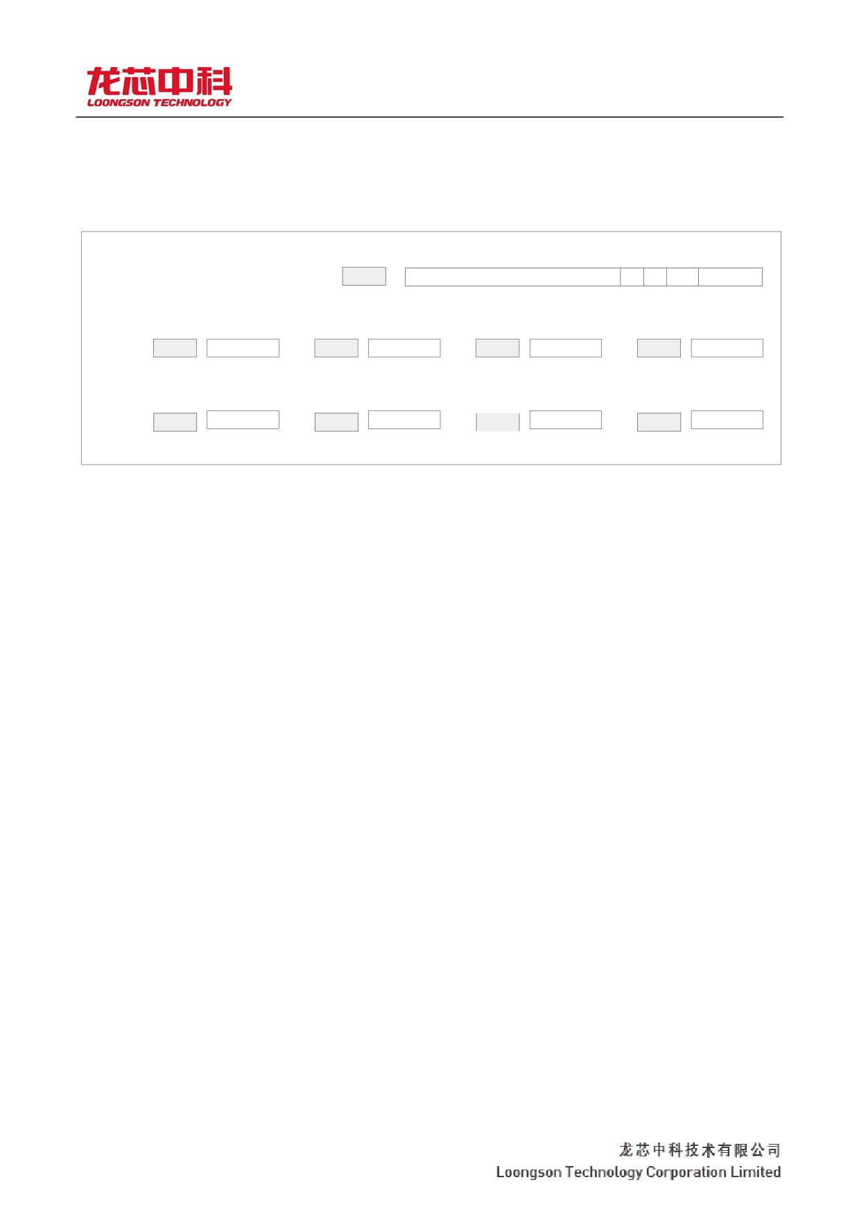
in the hit path. Figure 5-4 shows the structure of the cached row. In addition to the high (PTAG) position of the
physical address, the Tag includes cached line state information (CS), dirty Tag bit (W), instruction Tag (I), and
64
龙芯 3A3000/3B3000 处理器用户手册 y 下册
information about which way the cached line is located in the S-cache (SCWAY). Cs =0 means the cache row is
invalid; Cs =1 means that the cached rows are in a Shared state; Cs =2 indicates that the cached row is in an
exclusive state; Cs =3 is the reserved value. W =1 indicates that there is recently written data on the cache row.
I=1 means the cache line stores instruction, I=0 means the cache line stores data.
Figure 5-4 shows the level 2 sacrifice cache row structure
7043
8, 76, 54. 3
0
The
ecc_t
ptag
i.
W.
cs
scway
8
36
1 b. 1 b2b
4
6356, 511,
448
5548, 447,
384
4740, 383,
320
3932, 319,
256
ecc_d7
block7
ecc_d6
block6
ecc_d5
block5
ecc_d4
block4
8
64
8
64
8
64
8
64
The
3124, 255,
192
2316, 191,
128
158, 127,
64
7
0 63
0
ecc_d3
block3
ecc_d2
block2
ecc_d1
block1
ecc_d0
block0
8 b
64 b,
8 b
64 b,
8 b
64 b,
8 b
64
b,
At the second level, the "Sec-ded" ECC check is used to check the Tag and Data sections in the cached row.
When a new cache row is updated into the sacrifice cache, the Data section takes blocks as the basic unit of
verification, and each block generates 8-bit verification results and records them. After part 0 of Tag is extended to
64 bits, the same verification algorithm is used to generate 8-bit verification results, which are also recorded. When
reading the Cache, the original data and the reference check value are read out at the same time, and the original
data is recalculated and compared with the reference check value. If a bit error is found, the hardware will
automatically correct the error, fill the corrected value back into the V-cache, and record the relevant location
information, triggering an exception. If the error
65
龙芯 3A3000/3B3000 处理器用户手册 y 下册
If the digit exceeds one bit, the hardware cannot correct it. It should be noted that when the software fills the
Data Cache with Store Tag and Store Data class Cache instructions, it must simultaneously calculate the ECC
check value of the filled content and explicitly Store the ERRctL. ECC field. When the hardware executes such
Cache instructions, the reference checksum written in the Cache is sacrificed from the errctl.ECC field instead of
the hardware circuit's automatic checksum generation result. This mechanism is mainly used to complete some
special diagnosis. The algorithm for generating and detecting ECC check values at the expense of the cache is
consistent with the data cache, see section 5.1.3 on page 61.
5.1.5 Level 3 Shared Cache (S-Cache)
The three-level Shared cache supports cache consistency based on the directory protocol. Simongson 3A3000
chip s-Cache addresses all the chips uniformly, and each Shared Cache row has a fixed home node.
Split structure of Shared cache
The S-Cache of The Loongson 3A3000 chip is divided into four units (Banks) and receives access requests
from the processor core and I/O ports to maintain Cache consistency through the first-level cross-switch
interconnection network. Since longson 3A3000 chip adopts the address window mapping mechanism that can be
dynamically adjusted by software on the first-level cross-switch interconnection network, the physical address seen
by each S-cache body is the address remapped through the address window. Please make this clear when the
software operates S-Cache. Which of the four S-cache-bodies the different requests end up in is determined by the
two bits in the address that are dynamically adjusted by the software, as determined by the SCID_SEL of the chip
configuration register. The correspondence between the configuration information and the address bit of the s-
cache body is given. Accordingly, which bits of the physical address are used to cache the row index changes as
the SCID_SEL value changes.
Table
5-2 Three levels of Shared cache body selection bit and
index
address
SCID_SEL
Select a body
The index
value
address
b0000
PAddr [but]
PAddr [he]
b0001
PAddr [and]
{PAddr [and], PAddr [but]}
b0010
PAddr [10]
{PAddr [went], PAddr [or]}
b0011
PAddr [12]
{PAddr [thou doest, PAddr [but]}
b0100
PAddr [also]
{PAddr [before], PAddr [he]}
B0101 ~ b1111
PAddr [that is]
PAddr [and]
Locking mechanism for Shared cache
The capacity of the Shared cache unit is 2MB, and the 16-way group linkage structure is adopted. In addition
to using the LRU algorithm to select replacements, the Shared cache also supports cache locking mechanisms.
There are two ways to lock a Cache: one is to lock a Cache line using the Cache15 instruction; The other is to use
the Shared cache lock window mechanism in the chip configuration register to lock the physical address space.
Once the locked content is stored in the Shared Cache, it will not be replaced again, unless the following two
situations occur :(1) all Cache lines in 16-way s-cache that are locked with the locked Cache line and Index are in
the "locked" state, then all Cache line locks are deemed invalid, and the replacement item is still selected according
to LRU algorithm;
(2) Invalid "locked" Cache line using the software Cache instruction. The advantage of using
the Cache15 instruction is that it can directly use the virtual address to lock the Cache operation, and if the data is
not in s-cache, the Cache line to be locked will be retrieved to S-cache and then locked. The disadvantage is that
both the Cache lock and release operations need to be carried out in each Cache line, which has certain overhead.
66
龙芯 3A3000/3B3000 处理器用户手册 y 下册
Using lock window mechanism is to configure the advantages of a (write three window lock configuration register)
can lock in a large contiguous address space (not less than 15/16 of the S - Cache capacity in theory, namely 3.75
MB), the disadvantage is that configuration must have a physical address information, need special support, the
operating system kernel and configuration does not ensure that the data must be in the S - after the Cache. Software
personnel can select the appropriate S-Cache lock mechanism for program optimization according to the specific
characteristics of the application. See section 2.4.9 on page 33 for a detailed definition of the Cache15 directive.
For a detailed definition of the S-Cache lock window configuration register, see the description in section 2.5 of the
Loongson 3A300/3B3000 Processor User manual volume I.
The cache line structure of the Shared cache
The Shared cache USES the physical address index physical address label access mode. The data portion of
each cached row is 64 bytes long, divided into 8 bytes
Eight 8-byte wide blocks. The usual access is always to read or write all the Data parts in the Cache line, only
when the Load Data and Store Data class Cache instructions are executed with the two adjacent parity units as the
basic unit, at this time the physical address of the [5:4] is used to indicate which pair of adjacent parity blocks to
operate.
During access, the physical address high position is compared with the contents read by tags in each path to
determine whether the Cache is hit. If it hits, it reads out the data content of the corresponding cache block in the
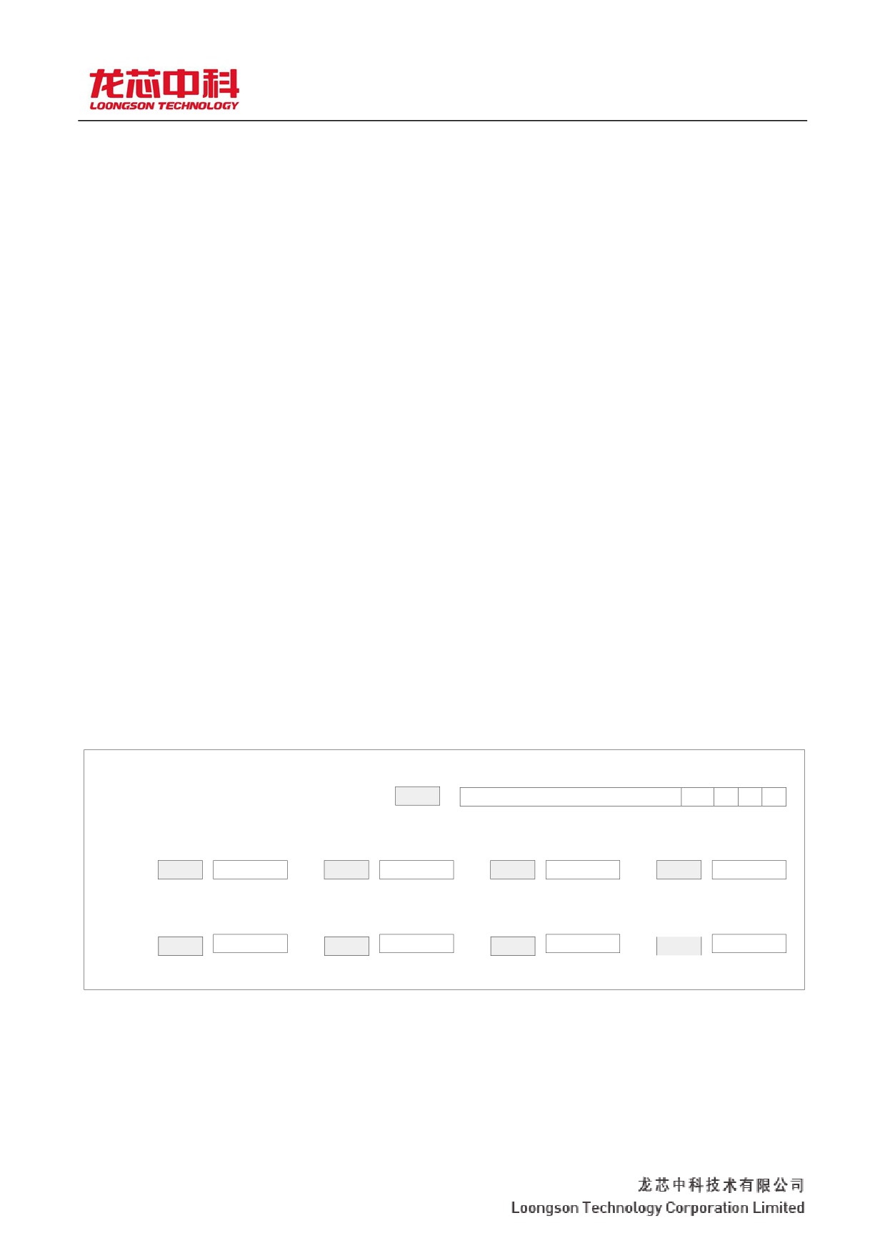
hit path. Figure 5-5 shows the structure of the Shared cache row. In addition to the high position (PTAG) of the
physical address, the Tag also includes cache line status information (SS), directory status information (DS), dirty
bit (W), page coloring bit (PGC). Ss =1 means the cache line is valid, ss=0 means the cache line is invalid. Ds =1
means the directory is dirty, ds=0 means the directory is clean. W =1 indicates that there is recently written data on
the cache row. Indicates that there is recently written data on the cache row. Page coloring bits are used by
hardware to handle cache aliases, see 69 for details
This is described in section 5.4.5.
Figure 5-5 shows the three-level Shared cache row structure
7036
5 43 210
The
ecc_t
ptag
ss
W.
ds
ss
8
32
2 b1b 1 b, 1 b
6356, 511,
448
5548, 447,
384
4740, 383,
320
3932, 319,
256
ecc_d7
block7
ecc_d6
block6
ecc_d5
block5
ecc_d4
block4
8
64
8
64
8
64
8
64
The
3124, 255,
192
2316, 191,
128
158, 127,
64
7
0 63
0
ecc_d3
block3
ecc_d2
block2
ecc_d1
block1
ecc_d0
block0
8 b
64 b,
8 b
64 b,
8 b
64 b,
8 b
64
b,
Shared cache validation
The third-level Shared cache USES the "Sec-ded" ECC check to check the Tag and Data sections in the
cached row. When a new cache row is updated into the Shared cache, the Data section takes blocks (blocks) as the
basic unit of verification, and each block generates 8-bit verification results and records them. After part 0 of Tag
is extended to 64 bits, the same verification algorithm is used to generate 8-bit verification results, which are also
recorded. When reading the Cache, the original data and the reference check value are read out at the same time,
67
龙芯 3A3000/3B3000 处理器用户手册 y 下册
and the original data is recalculated and compared with the reference check value. If a bit error is found, the
hardware will automatically correct the error, fill the corrected value back into S-cache, and record the relevant
location information, triggering an exception. If the error number exceeds one bit, the hardware will not be able to
correct it. It should be noted that when the software fills the Data Cache with Store Tag and Store Data class Cache
instructions, it must simultaneously calculate the ECC check value of the filled content and explicitly Store the
ERRctL. ECC field. When the hardware executes such Cache instructions, the reference checksum written in the
Cache is sacrificed from the errctl.ECC field instead of the hardware circuit's automatic checksum generation result.
This mechanism is mainly used to complete some special diagnosis. The algorithm for generating and detecting
ECC check values at the expense of the cache is consistent with the data cache, see section 5.1.3 on page 61.
5.2 The cache algorithm has the same properties as the cache
GS464E supports three caching algorithms and cache consistency properties: Uncached, Cacheable cache, and
Uncached Accelerated. The consistent algorithm corresponding to the non-cache algorithm is coded as 0b010, the
consistent algorithm corresponding to the consistent cache algorithm is coded as 0b011, and the consistent
algorithm corresponding to the non-cache acceleration algorithm is coded as 0b111.
5.2.1 Non-cache algorithm
When an address segment or page adopts a non-cache algorithm, the retrieval or memory operation of virtual
address on the address segment or page will be directly initiated by the processor to the location of the target
address, and the data read or written will not originate or terminate at any level of cache.
All access requests using a non-cached algorithm are executed in a blocking order. That is, before the current
read request data is returned to the processor, all subsequent requests are blocked and issued; All subsequent
requests are blocked until the write request data has been sent or the issued write request has not received a write
reply from the final receiver.
5.2.2 Consistent caching algorithm
When an address segment or page USES a non-cached algorithm, the content accessed by the pointer or fetch
operation that falls on the address segment or page can reside in any level of cache. GS464E is maintained by
hardware and does not require software to maintain Cache consistency by using invalid Cache instructions and
writing back the contents of the Cache.
5.2.3 Non-cache acceleration algorithm
The non-cache acceleration algorithm attribute is used to optimize a sequence of Uncached number operations
of the same type completed in a contiguous address space. The optimization method is to collect the memory
operation of this algorithm property by setting buffer. Data from these number operations can be stored in the
buffer as long as the buffer is not full. The buffer size is the same as a Cache line and is 64 bytes. A save operation
completes when the data is stored in a buffer. When the buffer data collection is full, it is written out consecutively
at once. Data written out in succession will be written directly to the destination address and will not stay in any
level of cache. During the data collection of sequential memory instruction, if a normal type of non-cached memory
instruction is inserted, the collection is aborted and the saved data in the buffer is output as byte writes. The
operation effect of the finger or number operation of the non-cache acceleration algorithm attribute is the same as
68
龙芯 3A3000/3B3000 处理器用户手册 y 下册
that of the normal non-cache algorithm attribute.
The non-cache acceleration attribute speeds up sequential Uncached access and is suitable for quick output
access to display device storage.
5.3 Cache consistency
GS464E implements the directory based Cache consistency protocol, which ensures the consistency of data
among I-cache, D-cache, V-cache, S-cache, memory and IO devices from HT by hardware, and does not require
software to use Cache instructions to maintain Cache consistency.
Each Cache line in GS464E has a fixed host S-cache body. The directory information for the Cache rows is
maintained in the host S-cache body. The directory USES a 64-bit bit vector to record the first level of caches
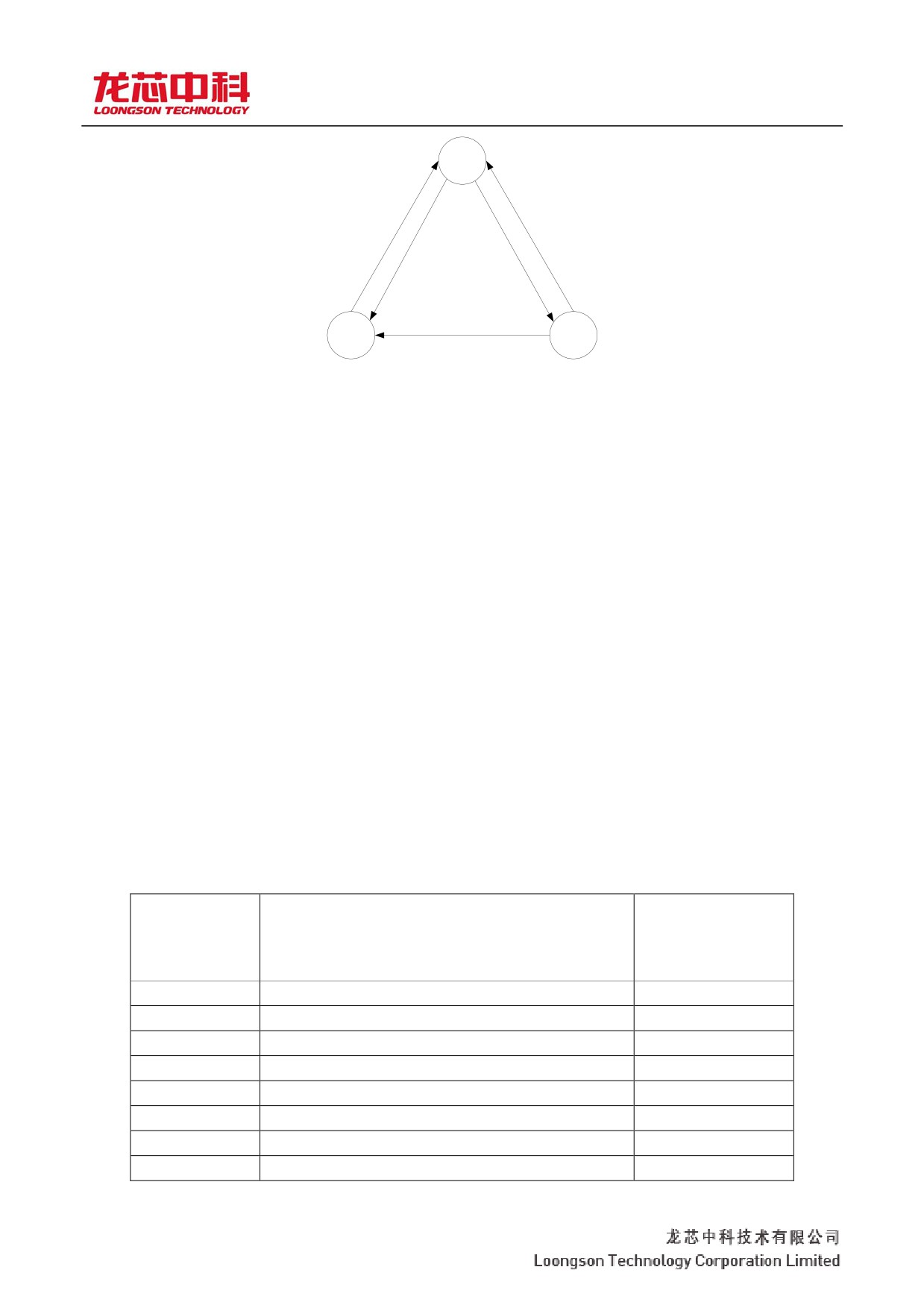
(including i-cache and D-cache) that have a backup of each Cache row. Each level Cache block has three possible
states: INV (invalid state), SHD (Shared state, readable), and EXC (exclusive state, readable, writable). The
transitions between the three states are shown in Figure 5-6.
When the read instruction or fetch operation fails in the first and second level caches, the processor core issues
a Reqread request to the third level S-Cache. After receiving the Repread reply returned by S-Cache, the processor
core's first level Cache obtains a copy of the Cache line in the state of SHD. When the Cache operation fails in
both the first and second level caches, the processor core issues a Reqwrite request to the third level S-Cache. After
receiving a Repwrite reply returned by S-cache, the processor core's first level Cache obtains a backup of the Cache
line in the state of EXC.
When a V-cache replacement occurs to the processor core, Reqreplace writes back to the S-Cache module, and
s-Cache replies via Repreplace to inform the processor that the core replacement request has been processed.
S-cache can be backed up with an invalid SHD Cache line in i-cache, D-cache, or V-cache by sending a
Reqinv request to the processor core. The processor core changes the corresponding Cache line to INV and replies
to s-cache with Repinv. S-cache can write back an EXC backup of the Cache line by sending a Reqwtbk request to
the processor core, which returns the corresponding Cache line backup to the SHD state and replies to s-cache via
Repwtbk. S-cache can write back to the processor core by sending a Reqinvwtbk request that invalidates an EXC
backup of the Cache line. The processor core returns the backup of the corresponding Cache line to an INV state
and replies to a second-level Cache module via Repinvwtbk.
Figure 5-6 Cache state transitions under conformance protocol
69
龙芯 3A3000/3B3000 处理器用户手册 y 下册
INV
ReqInv
ReqInvwtbk
ReqReplace
ReqReplace
ReqReadReqWrite
SHD
EXC
ReqInvwtbk
5.4 Cache management
5.4.1 CACHE directives
This processor implements CACHE instructions for I- CACHE, D- CACHE, V- CACHE, and S- CACHE.
The format of the CACHE instruction is CACHE OP, offset(Base). There are some differences between the
GS464E Cache directive and the MIPS64 specification, as detailed in section 2.4.9 on page 33. Again, the MIPS
specification does not apply to GS464E if the object being manipulated is level 2 or level 3 Cache based on
op[1:0]=2 or =3. To reserve the software as forward-compatible as possible, OP [1:0]=2 indicates that the
operation object is S-Cache(level 3), and OP [1:0]=3 indicates that the operation object is V-Cache(level 2). In this
code form, software code that USES S-cache brush to maintain Cache consistency on the 3A1000 chip can still
achieve the same Cache consistency on the 3A3000 chip. In other words, when the software is invalid in an S-
cache line, the hardware guarantees that the same physical address in the Cache of all processor cores will be
invalid at the same time. When the software is invalid and written back to an S-cache line, the hardware ensures
that the same physical address is invalidated simultaneously in the caches of all processor cores, and that the
contents written back to main memory must contain the most recently written data.
CACHE instruction in root mode
Kernel mentality software running in root mode can use all implemented CACHE instructions, the list is as
follows:
Table 5-3 CACHE instructions in root mode
Op [4-
Function
Objective
0]
al
the Cache
descript
ion
b00000
Invalid Cache line based on index
I - Cache
b01000
Writes the Cache line Tag against the index
I - Cache
b11100
Writes the Cache row Data against the index
I - Cache
b00001
Invalid index and writes back to Cache line
D - the Cache
b00101
Read the Cache line Tag against the index
D - the Cache
b01001
Writes the Cache line Tag against the index
D - the Cache
b10001
Invalid Cache line based on hit
D - the Cache
b10101
Invalid hit and writes back to Cache line
D - the Cache
70

龙芯 3A3000/3B3000 处理器用户手册 y 下册
b11001
Read the Cache row Data against the index
D - the Cache
b11101
Writes the Cache row Data against the index
D - the Cache
b00010
Invalid index and writes back to Cache line
V - Cache
b00011
Invalid index and writes back to Cache line
S - the Cache
b00111
Read the Cache line Tag against the index
S - the Cache
b01111
Retrieve and latch the Cache line based on the
S - the Cache
address
71
龙芯 3A3000/3B3000 处理器用户手册 y 下册
Op [4-
Function
Objective
0]
al
the Cache
descript
ion
b01011
Writes the Cache line Tag against the index
S - the Cache
b10011
Invalid hit and writes back to Cache line
S - the Cache
b11011
Read the Cache row Data against the index
S - the Cache
b11111
Writes the Cache row Data against the index
S - the Cache
The CACHE2 instruction is mainly used to clear the V-cache of a single core when it is only closed. The
hardware only guarantees the correctness of the result when using CACHE2 in the following way.
First, when using the CACHE2 instruction to clear the V-cache, make sure that all code executed during this
process is in the uncache space. Second, when using the CACHE2 instruction to clear the V-cache, do not perform
any other load or store operations in the Cache space.
Use of CACHE instructions in guest mode
The use of CACHE instructions in guest mode is controlled by the root mode, which is defined as follows:
z When guestCTL0.cg =0, the use of any CACHE instruction will trigger the guest mode privileged sensitive instruction
exception (GPSI).
z When guestCTL0.cg =1, CACHE instruction with OP [4:2]=1, 2, 6, 7 will trigger the guest mode privileged sensitive
instruction exception (GPSI).
z When guestCTL0.cg =1, but Dig.GCAc =0, CACHE0, CACHE1, CACHE3 will trigger the guest mode
privileged sensitive instruction exception (GPSI).
5.4.2 Cache initialization
Hardware-based cache initialization
During a hard restart, the hardware sets all the cached Tag parts to all zeros, making all cached Cache lines
invalid. Therefore, the software does not need to initialize all caches except for the following special use case.
A special case that makes hardware initialization Cache unsafe is when, after a hard restart of the processor,
the software USES the Index Store Tag instruction to make a Cache line valid, but does not use the Index Store
Data instruction to make all the blocks of the Data section of that Cache line certain.
If the above sequence of actions does exist in the software, be sure to initialize the cache in a software-like
manner before performing an action that poses a security risk.
Software-based cache initialization
67
龙芯 3A3000/3B3000 处理器用户手册 y 下册
The software based cache initialization process recommended by GS464E is as follows:
Step 1: Create a chunk of memory to fill with arbitrary data. This data is then used to populate the cached
data portion to form the correct checksum. It is recommended to use a memory area starting at address
0.
Step 2: Mask interrupts to prevent unexpected
situations during initialization. Step 3:
Initialize i-Cache.
Mtc0 zero, TagLo;
Mtc0 zero, TagHi;
Mtc0 zero, ErrCtl;
The parity of /* 64-bit full 0 is 0x0*/
68
龙芯 3A3000/3B3000 处理器用户手册 y 下册
Cache_Index_Store_Tag_I (addr +
way);
For (block = 0;
Block <
8;
Block + = 1) {
Cache_Index_Store_Data_I (addr + (block < < 3) + way);
}
}
}
Step 4: Initialize the D-cache.
Mtc0 zero, TagLo;
Mtc0 zero, TagHi;
Addiu r1, r1, 0 x22;
Mtc0 r1, ErrCtl;
The ECC check value
for /* 64-bit full 0 is 0x22*/ for (addr= 0xffFFFFFF80000000;
Addr < 0 xffffffff80010000;
Addr + = 64) {
*/ for (way=0;
Way < 4;
Way + = 1) {
Cache_Index_Store_Tag_D (addr +
way);
For (block = 0;
Block <
8;
Block + = 1) {
Cache_Index_Store_Data_D (addr + (block < < 3) + way);
}
}
}
Step 5: Initialize V-Cache.
Mtc0 zero, TagLo;
Mtc0 zero, TagHi;
Addiu r1, r1, 0 x22;
Mtc0 r1, ErrCtl;
The ECC check value
for /* 64-bit full 0 is 0x22*/ for (addr= 0xffFFFFFF80000000;
Addr < 0 xffffffff80010000;
Addr + = 64) {
*/ for (way=0;
Way < 16;
Way + = 1) {
Cache_Index_Store_Tag_V (addr + way);
For (block_pair = 0;
Block_pair < 4;
Block_pair
+ = 1) {Cache_Index_Store_Data_V (addr +
(block_pair < < 4) + way);
}
}
}
Step 6: Initialize S-Cache. 1
Scache_init_ok [get_my_CPUNum ()] = 0;
/* Use uncached
Write */ MTC0 Zero, TagLo;
Mtc0 zero, TagHi;
Addiu r1, r1, 0 x22;
Mtc0 r1, ErrCtl;
The ECC check value for /* 64-bit full 0 is
0x22*/
Processor no. 0 initializes s-Cache Bank no. 1, and so on */ Bank =
get_my_CPUNum();
69
龙芯 3A3000/3B3000 处理器用户手册 y 下册
For (addr = 0 xffffffff80000000;
Addr < 0 xffffffff80040000;
Addr + = 256) {
*/ for (way=0;
Way < 16;
Way + = 1) {
The chip configuration register SCID_SEL is equal to the default value of 0.
70
龙芯 3A3000/3B3000 处理器用户手册 y 下册
Cache_Index_Store_Tag_V (addr + (bank < < 6) + way);
For (block_pair = 0;
Block_pair < 4;
Block_pair + = 1)
{Cache_Index_Store_Data_V (addr + (bank < < 6) + (block_pair
< < 4) + way);
}
}
}
Scache_init_ok [get_my_CPUNum ()] = 1;
/* Use uncached write*/
Step 7: Poll the Scache_init_ok vector until all items are 1.
/* Polling should use uncached Read */
At this point, the cache is initialized.
5.4.3 Maintain consistency between level 1 instruction cache and level 1 data cache
For applications with "self-modifying code," there is a problem of data consistency between the first-level
instruction cache and the first-level data cache. GS464E is maintained by the hardware for data consistency
between the first-level instruction CACHE and the first-level data CACHE without the need for software to use the
CACHE instruction or SYNCI instruction to maintain data consistency by brushing back and clearing the D-cache
and i-cache.
It should be noted that GS464E implements a weakly consistent storage model. So after the software has
modified the code, it must jump to the modified code using the JR. Hb or JALr. hB instructions. In addition to the
jump, JR. Hb and jalr. HB act as barriers. This ensures that the PC at the target of the JR. Hb or JALr. HB jump
will see the modified front gate write operation.
5.4.4 Maintain cache consistency between processor and DMA device
In order to improve the performance of the processor, the driver software of DMA devices will put the data
requiring a large amount of interaction in the cache space, thus causing the cache consistency maintenance problem
between the processor and DMA devices. This issue is addressed in detail in many driver development books and
is not covered in this manual. In the Loongson 3A3000 chip, the hardware can maintain cache consistency between
the processor and DMA devices connected to the HT port. Therefore, when a DMA device in the system accesses
system main memory through HT port, the driver software of the device does not need to use Cache instruction to
maintain data consistency by swiping S-cache. Doing so can improve processor performance.
It should be noted that GS464E implements a weakly consistent storage model. Therefore, between the
processor and DMA equipment, the synchronization effect of the gate barrier still needs to be achieved through the
semaphore stored in the uncached area or the interrupt mechanism, so as to ensure that consumers can actually
observe the data the producer wants them to observe when they read the data.
5.4.5 Cache alias and page coloring
Because GS464E's first-level instruction cache and first-level data cache use the access mode of virtual index
physical labels, and each cache path is 16KB in size, there is a cache alias problem when the page size is 4KB or
70
龙芯 3A3000/3B3000 处理器用户手册 y 下册
8KB. The popular solution to cache aliases is a "page coloring" mechanism, which guarantees that at any given
time, a physical address has at most one "page color" of a virtual address. GS464E implements the "page coloring"
mechanism through hardware and is no longer implemented by software.
In the vast majority of cases, the software can ignore cache aliases because the hardware is guaranteed by
"page coloring" that cache aliases do not occur. The only exception is when the software USES the Index Store
Tag and Index Store Data class Cache directives to create valid Cache rows directly from each level of the Cache
and USES the Data from those Cache rows with subsequent programs. At this point, the software must ensure that
the contents of the page color field (PGC) in the S-cache line Tag match the virtual address of the Cache line data.
Specifically, the PGC field in the Tag of S-Cache must always be equal to the [13:12] bit of the virtual address of
the Cache line.
71
龙芯 3A3000/3B3000 处理器用户手册 y 下册
6 Processor exceptions and interrupts
6.1 Processor exception
6.1.1 Exception priority
When an instruction meets more than one exception trigger condition at the same time, GS464E will trigger
the exception with higher priority according to the example in Table 6-1.
Table 6-1 Exception priorities
exce
type
ptio
n
Cold reset
Asynchronous, reset classes
EJTAG performs the one-step exception
Synchronize and debug classes
EJTAG debug interrupt exception
Asynchronous, debug class
Non-masking interrupt
asynchronous
EJTAG instruction breakpoint exception
Synchronize and debug classes
The wrong address exception - pointing
synchronous
TLB/XTLB refill exception - take finger
synchronous
TLB invalid exception - pointing
synchronous
TLB performs blocking exceptions
synchronous
Cache error exception - pointing
synchronous
EJTAG SDBBP exception
synchronous
No exceptions can be made to the coprocessor
synchronous
Reservation instruction exception
synchronous
interrupt
asynchronous
Integer overflow exception, trap exception, system
synchronous
call exception, breakpoint
Exceptions, floating point exceptions, floating point
stack exceptions
Exception for EJTAG exact data breakpoint
Synchronize and debug classes
The wrong address exception - Data access
synchronous
TLB/XTLB refill exception - Data access
synchronous
Invalid exception for TLB - Data access
synchronous
TLB reads prevent exceptions
synchronous
TLB modification exceptions
synchronous
Cache error exception - Data access
synchronous
6.1.2 Exception entry vector position
Cold reset, soft reset, and non-masking interruptible exception entry vector addresses use the dedicated
72
龙芯 3A3000/3B3000 处理器用户手册 y 下册
address 0xffff.ffff.bfc0.0000, which is neither cache-accessible nor address-mapped.
Vector addresses of EJTAG debugging related exceptions are selected according to whether the ProbeTrap bit
in the EJTAG control register is 0 or 1
0 XFFFF. FFFF. BFC0.0480 and 0 XFFFF. FFFF. FF20.0200.
73
龙芯 3A3000/3B3000 处理器用户手册 y 下册
All other exception vector addresses are defined as "base address + offset". When status. BEV=0, the base
address of all exceptions adopts fixed configuration; When status. BEV=0, the software can configure the
exception vector base address through the EBase register and the GSEBase register. Table 6-2 lists the exception
vector base address definitions, and Table 6-3 lists the exception offset definitions.
Table 6-2 exception vector base addresses
exce
Status. BEV = 0
Status. BEV = 1
ptio
n
Cold reset, soft reset, non-masking
0 XFFFF. FFFF. BFC0.0000
interrupt
EJTAG debugging exception
0 XFFFF. FFFF. BFC0.0480
(ProbTrap=0)
EJTAG debugging exception
0 XFFFF. FFFF. FF20.0200
(ProbTrap=1)
Cache fault exception
EBase || 1 || EBase || 0x000 63..3028..12
0 XFFFF. FFFF. BFC0.0200
Other Exceptions
EBase | | 0 x000 63..12
0 XFFFF. FFFF. BFC0.0200
Table 6-3 exception vector offset
exce
The vector offset
ptio
n
Cold reset, soft reset, non-masking interrupt
No offset, use base address directly
All kinds of EJTAG debugging exceptions
No offset, use base address directly
(ProbTrap=0)
Various EJTAG debugging exceptions (ProbTrap=1)
No offset, use base address directly
TLB refill exception (status.exl =0)
0 x000
XTLB refill exception (status.exl =0)
0 x080
Cache fault exception
0 x100
Other Exceptions
0 x180
Interrupt (Cause. IV = 0)
0 x180
Interrupt (intCTL.vs =0 and cause.IV =1)
0 x200
Interruption (status.bev =1 and cause.iv =1)
0 x200
interrupt
0X200 + (interrupt vector no. × (intctl.vs || 0b00000))
(caus.iv =1 and status.bev =0 and intctL.vs! = 0)
6.1.3 The processor hardware responds to the exception's generic processing
When the processor starts processing an exception, the EXL bit of the status register is set to 1, meaning that
the system is running in kernel mode. After saving the appropriate field state, the exception handler
usually sets the KSU field of the state register to kernel mode, while returning the EXL position to 0. When the
field state is restored and re-executed, the handler restores the KSU field to its previous value and sets the EXL bit
to 1.
74
龙芯 3A3000/3B3000 处理器用户手册 y 下册
Returning from an exception also sets the EXL position to 0.
6.1.4 Cold reset exception
A cold reset exception occurs when the system is powered on or cold reset for the first time. This exception
cannot be blocked.
The cold reset exception USES a special exception entry vector address. The address belongs to a CPU that
does not require address mapping and does not access data through a Cache
Address space, so processing this exception does not have to initialize TLB or Cache. This also means that
even if the Cache and TLB are in an uncertain state,
75
龙芯 3A3000/3B3000 处理器用户手册 y 下册
The processor can also fetch and execute instructions.
When a cold reset exception occurs, the processor goes through a full reset initialization process in which the
contents of all registers in the CPU are uncertain, except for the following register fields:
z The Status register is set to the initial value, with SR bit 0, ERL bit and BEV bit 1.
z
Initial value of Config0~Config6 register.
z
The Random register is initialized to the maximum value, and the Wired register is initialized to 0.
z
Initial values of related fields for EntryHi, EntryLo0, EntryLo1, PageMask, PageGrain.
z
The ErroEPC register is initialized to the value of the PC.
z
The Event bit of the Performance Count register is initialized to 0.
z
All breakpoints and external interrupts are cleared.
6.1.5 Non-masking interrupt
Non-masking interrupts are triggered by a processor-independent NMI interrupt input signal. This exception
cannot be blocked.
It is not possible to mask interrupts with exception entry vectors consistent with cold reset. Therefore, in the
event of an unmasking interrupt exception, the status.NMI bit is set to 1 and the software can distinguish a cold
reset by the bit.
The non-masking interrupt exception does not discard the state of any machine, but rather retains the state of
the processor for diagnostic purposes. In particular, the Cause register contents remain unchanged, while the system
jumps to an unmasked exception entry vector to start executing the handler.
The non-masking interrupt exception only modifies the following registers:
z
Status.ERL is 1, status. SR is 0, status. NMI is 1, and status. BEV is 1.
z The ErroEPC register is initialized to the value of the PC.
6.1.6 Interrupt exception
An interrupt exception is triggered when an unmasked interrupt arrives. For a detailed
description of interrupts, refer to section 6.2 on page 80. Control register Cause's ExcCode
field:
0x00 (Int) (see table 7-28 on page 111)
Additional hardware status updates in
response to exceptions:
register
Status
update
description
Cause
The IP domain records the interrupts to be processed.
6.1.7 Wrong address exception
76
龙芯 3A3000/3B3000 处理器用户手册 y 下册
The address error exception is triggered when:
Double-word load/store, whose access address is
not aligned at the double-word boundary. The
access address of the word load/store is not
aligned at the word boundary.
Half-word load/store instruction, its access
address is not aligned with the half-word
boundary. Point PC not aligned at word
boundary.
Access the address segment of the core mode
in customer mode or regulatory mode. Access
the regulatory mode address segment in
customer mode.
77
龙芯 3A3000/3B3000 处理器用户手册 y 下册
When 64-bit addressing enablement is not enabled, the access to the PC or Load/Store instruction USES a 64-
bit address, and the address falls outside the 32-bit address space compatibility range.
Refers to the PC or load/store instruction access using a
64-bit address, and the address falls in the
unimplemented range. In core mode, the page table entry accessed is valid and the K bit is 0.
This exception can be handled in both root and guest modes. Control register Cause's ExcCode field:
0x04 (AdEL) : Finger or read
data AdES (0x05) : write data
(See Table 7-28, page 111)
Additional hardware status updates in response to exceptions:
register
Status
update
description
BadVAddr
Record the virtual address that triggered the exception.
6.1.8 TLB rewrites the exception
In 32-bit host address space, and root.status.exl =0, access memory USES mapped address, which triggers
TLB refill exception when no match is found in TLB. Note that this is different from the case where a match is
found in TLB but the matching page table entry has a valid bit of 0, which corresponds to an invalid exception for
TLB. To speed up the processing efficiency of frequent and critical exceptions such as TLB refill, the TLB refill
exception USES a separate exception entry offset, so the exception coded in the root.cause.Exccode field is not
distinguished from the XTLB refill exception and the TLB invalid exception.
This exception is handled only in root mode.
Control register Cause's ExcCode field:
0x02 (TLBL) : To pick up or read data
0x03 (TLBS) : Write data
(See Table 7-28, page 111)
Additional hardware status updates in response to exceptions:
registe
Status
r
update
description
BadVAddr
Record the virtual address that triggered the exception.
The
The BadVPN2 domain record triggers the [31..13] bit of an exception's virtual
Context
address.
XContext
?
VPN2 domain record triggers the virtual address of the exception [47..13] bit;
EntryHi
The R field record triggers the [63..62] bit of an exception's virtual address.
The ASID domain records the ASID of the process to which the exception is
triggered.
Diag
The MID field is set to 0.
6.1.9 XTLB rewrites the exception
78
龙芯 3A3000/3B3000 处理器用户手册 y 下册
Under the 64-bit host address space, and root.status.exl =0, access memory USES mapped address, which
triggers XTLB refill exception when no match is found in TLB. Note that this is different from the case where a
match is found in TLB but the matching page table entry has a valid bit of 0, which corresponds to an invalid
exception for TLB. To speed up the processing efficiency of the frequent and critical exception XTLB refill, the
XTLB refill exception USES a separate exception entry offset, so the exception encoded in the root.cause.Exccode
field is not distinguished from the TLB refill exception and the TLB invalid exception.
79
龙芯 3A3000/3B3000 处理器用户手册 y 下册
This exception is handled only in root mode.
Control register Cause's ExcCode field:
0x02 (TLBL) : To pick up or read data
0x03 (TLBS) : Write data
(See Table 7-28, page 111)
Additional hardware status updates in response to exceptions:
registe
Status
r
update
description
BadVAddr
Record the virtual address that triggered the exception.
The
The BadVPN2 domain record triggers the [31..13] bit of an exception's virtual
Context
address.
BadVPN2 domain record triggers the virtual address of the exception [47..13]
XContext
bit;
The R field record triggers the [63..62] bit of an exception's virtual address.
VPN2 domain record triggers the virtual address of the exception [47..13] bit;
EntryHi
The R field record triggers the [63..62] bit of an exception's virtual address.
The ASID domain records the ASID of the process to which the exception is
triggered.
Diag
The MID field is set to 0.
6.1.10 TLB is not an exception
The TLB invalid exception is triggered when:
The map address is used in the host address space. The match is found in TLB, but the valid bit of the match
page table entry is 0. This exception is triggered.
When PageGrain. IEC = 0
Pagegr.rie =1, load operation USES mapped address in the host address space, matching and valid items are
found in TLB, but the RI bit in the table entry is 1.
Pagegry.xie =1, refers to the use of mapping address in the host address space, and finds a matching and valid
item in TLB, but the XI bit in the table entry is 1.
The software needs to pay attention to the following situation: when root.status. EXL=1, when the mapping
address used for access cannot find a match in TLB, the exception entry offset adopted is the normal exception
entry offset (0x180), and the exception encoding filled in the root.cause.ExcCode field is still TLBL (0x2) or TLBS
(0x3). To distinguish this from a normal INVALID TLB exception, only the exception handler can use the TLBP
instruction to distinguish based on the lookup results.
This exception is handled only in root mode.
Control register Cause's ExcCode field:
0x02 (TLBL) : To pick up or read data
0x03 (TLBS) : Write data
80
龙芯 3A3000/3B3000 处理器用户手册 y 下册
(See Table 7-28, page 111)
Additional hardware status updates in response to exceptions:
register
Status
update
description
BadVAddr
Record the virtual address that triggered the exception.
The Context
The BadVPN2 domain record triggers the [31..13] bit of an exception's virtual
address.
81

龙芯 3A3000/3B3000 处理器用户手册 y 下册
register
Status
update
description
BadVPN2 domain record triggers the virtual address of the exception [47..13]
XContext
bit;
The R field record triggers the [63..62] bit of an exception's virtual address.
VPN2 domain record triggers the virtual address of the exception [47..13] bit;
EntryHi
The R field record triggers the [63..62] bit of an exception's virtual address.
The ASID domain records the ASID of the process to which the exception is
triggered.
Diag
The MID field is set to 0.
6.1.11 TLB modification exceptions
The store operation maps the address in the host address space, which finds a matching and valid entry in TLB,
but the d-bit of the page table entry is 0 (meaning the page cannot be written), triggering the TLB modification
exception.
This exception is handled only in root mode.
Control register Cause's ExcCode field:
0x01 (Mod) (see Table 7-28 on page 111)
Additional hardware status updates in
response to exceptions:
registe
Status
r
update
description
BadVAddr
Record the virtual address that triggered the exception.
The
The BadVPN2 domain record triggers the [31..13] bit of an exception's virtual
Context
address.
BadVPN2 domain record triggers the virtual address of the exception [47..13]
XContext
bit;
The R field record triggers the [63..62] bit of an exception's virtual address.
VPN2 domain record triggers the virtual address of the exception [47..13] bit;
EntryHi
The R field record triggers the [63..62] bit of an exception's virtual address.
The ASID domain records the ASID of the process to which the exception is
triggered.
Diag
The MID field is set to 0.
6.1.12 TLB performs blocking exceptions
When root.pagegrb.IEC =0, and root.pagegrb.xie =1, take the mapping address under the host address space,
find a matching and valid item in TLB, but the XI bit in the table entry is 1.
This exception is handled only in root mode.
Control register Cause's ExcCode field:
0x14 (TLBXI) (see Table 7-28 on page 111)
Additional hardware status updates in
76

龙芯 3A3000/3B3000 处理器用户手册 y 下册
response to exceptions:
register
Status
update
description
BadVAddr
Record the virtual address that triggered the exception.
The Context
The BadVPN2 domain record triggers the [31..13] bit of an exception's virtual
address.
BadVPN2 domain record triggers the virtual address of the exception [47..13]
XContext
bit;
The R field record triggers the [63..62] bit of an exception's virtual address.
VPN2 domain record triggers the virtual address of the exception [47..13] bit;
EntryHi
The R field record triggers the [63..62] bit of an exception's virtual address.
The ASID domain records the ASID of the process to which the exception is
triggered.
77
龙芯 3A3000/3B3000 处理器用户手册 y 下册
register
Status
update
description
Diag
The MID field is set to 0.
6.1.13 TLB reads prevent exceptions
When root.pagegrb.IEC =0, and root.pagegrb.RIE =1, load operates under the host address space using
the mapped address in TLB
, but the RI bit in the table entry is 1. This
exception is handled only in root mode.
Control register Cause's ExcCode field:
0x13 (TLBRI) (see Table 7-28 on page 111)
Additional hardware status updates in
response to exceptions:
registe
Status
r
update
description
BadVAddr
Record the virtual address that triggered the exception.
The
The BadVPN2 domain record triggers the [31..13] bit of an exception's virtual
Context
address.
BadVPN2 domain record triggers the virtual address of the exception [47..13]
XContext
bit;
The R field record triggers the [63..62] bit of an exception's virtual address.
VPN2 domain record triggers the virtual address of the exception [47..13] bit;
EntryHi
The R field record triggers the [63..62] bit of an exception's virtual address.
The ASID domain records the ASID of the process to which the exception is
triggered.
Diag
The MID field is set to 0.
6.1.14 Cache error exception
This exception is triggered when a check error is found in the Cache tag or data during the fetch or load/store
operation. This exception cannot be blocked. Because the error involved in this exception is in the Cache, a
special exception entry is used in the non-mapped non-cached address segment. This exception entry is described
in section 6.1.2 on page 71.
This exception is handled only in root mode.
Control register Cause's ExcCode
field: none
Hardware status update
process in response to
exceptions: CacheErr
ErrorState Status.ERL 1
If InstructionInBranchDelaySlot then
78
龙芯 3A3000/3B3000 处理器用户手册 y 下册
ErrorEPC PC of the branch/jump
The else
ErrorEPC PC of the instruction
endif
If the Status. BEV = 1 then
PC xFFFF.FFFF.BFC0.0200 + 0 0 x100
The else
1 || PC 0 xFFFF.FFFF || EBase || EBase || 0 x100 endif
31..3028..12
79
龙芯 3A3000/3B3000 处理器用户手册 y 下册
6.1.15 Exception for integer overflow
Integer overflow is an exception when an ADD, ADDI, SUB, DADD, DADDI, or DSUB instruction executes,
resulting in a complement overflow.
This exception can be handled in both root and guest modes. Control register Cause's ExcCode field:
0x0C (Ov) (see Table 7-28, page 111)
Additional hardware status updates in
response to exceptions:
There is no
6.1.16 Trap exceptions
When the TGE, TGUE, TLT, TLTU, TEQ, TNE, TGEI, TGEUI, TLTI, TLTUI, TEQI, TNEI instructions are
executed,
The trap exception is triggered when the conditional result is true.
This exception can be handled in both root and guest modes. Control register Cause's ExcCode field:
0x0d (Tr) (see Table 7-28 on page 111)
Additional hardware status updates in
response to exceptions:
There is no
6.1.17 System call exception
The system call exception is triggered when the SYSCALL directive is executed. This exception can be
handled in both root and guest modes.
Control register Cause's ExcCode field:
0x08 (Sys) (see Table 7-28 on page 111)
Additional hardware status updates in
response to exceptions:
There is no
6.1.18 Breakpoint exception
The breakpoint exception is triggered when a BREAK instruction is executed. This exception can be handled
in both root and guest modes.
Control register Cause's ExcCode field:
0x09 (Bp) (see Table 7-28 on page 111)
Additional hardware status updates in
response to exceptions:
There is no
78
龙芯 3A3000/3B3000 处理器用户手册 y 下册
6.1.19 Reservation instruction exception
An exception to the retain instruction is triggered when a GS464E instruction is not implemented. This
exception can be handled in both root and guest modes.
79