Loongson 3A3000/3B3000 processor user manual. Part ii GS464E processor core V1.2 - page 4
龙芯 3A3000/3B3000 处理器用户手册 y 下册
PSUBUSB
Eight 8-bit unsigned integers minus, unsigned saturation
LoongEXT32
PSUBB
Eight 8-digit subtractions
LoongEXT32
PSUBD
64 digits
LoongEXT32
PSHUFH
The Shuffle has four 16-digit digits
LoongEXT32
PACKSSWH
32 bit signed integer converted to 16 bits, sign saturation
LoongEXT32
PACKSSHB
16 bit signed integer converted to 8 bit, sign saturation
LoongEXT32
PACKUSHB
16 bit signed integer converted to 8 bit, unsigned saturation
LoongEXT32
PANDN
Fs is not followed by ft bitwise and
LoongEXT32
68
龙芯 3A3000/3B3000 处理器用户手册 y 下册
Instruction
Instruction
ISA
mnemonic
function
Compatible
description
Category
PUNPCKLHW
Unpack is low by 16 digits
LoongEXT32
PUNPCKHHW
Unpack is 16 digits high
LoongEXT32
PUNPCKLBH
Unpack is low by eight digits
LoongEXT32
PUNPCKHBH
Unpack is eight digits high
LoongEXT32
PINSRH_0
The ft low 16 bits are inserted into the FS low 0 16 bits
LoongEXT32
PINSRH_1
The ft low 16 bits are inserted into the FS low 16 bits
LoongEXT32
PINSRH_2
The ft low 16 bits are inserted into the FS low 2 16 bits
LoongEXT32
PINSRH_3
The ft low 16 bits are inserted into the FS low 3 16 bits
LoongEXT32
PAVGH
Four 16-bit unsigned integers are averaged
LoongEXT32
PAVGB
Eight 8-bit unsigned integers are averaged
LoongEXT32
PMAXSH
Four 16-bit signed integers take a larger value
LoongEXT32
PMINSH
Four 16-bit signed integers take smaller values
LoongEXT32
PMAXUB
Eight 8-bit unsigned integers take a larger value
LoongEXT32
PMINUB
Eight 8-bit unsigned integers take smaller values
LoongEXT32
PCMPEQW
Two 32 - digit Numbers equal to compare
LoongEXT32
PCMPGTW
Two 32-bit signed integers are greater than the comparison
LoongEXT32
PCMPEQH
Four 16-digit Numbers are equal for comparison
LoongEXT32
PCMPGTH
Four 16-bit signed integers are greater than the comparison
LoongEXT32
PCMPEQB
Eight 8-digit Numbers are equal for comparison
LoongEXT32
PCMPGTB
Eight 8-bit signed integers are greater than the comparison
LoongEXT32
PSLLW
Two 32-bit logical moves left
LoongEXT32
PSLLH
Four 16-digit logical left shifts
LoongEXT32
PMULLH
Multiply four 16-bit signed integers and you get 16 bits lower
LoongEXT32
PMULHH
Multiply four 16-bit signed integers and take the result 16 bits higher
LoongEXT32
PMULUW
Multiply low 32 - bit unsigned integers and save 64 - bit results
LoongEXT32
PMULHUH
Multiply four 16-bit unsigned integers and take 16 bits higher
LoongEXT32
PSRLW
Two 32-bit logical moves to the right
LoongEXT32
PSRLH
Four 16-digit logical shifts to the right
LoongEXT32
PSRAW
Two 32-bit arithmetic moves to the right
LoongEXT32
PSRAH
Four 16-digit arithmetic moves to the right
LoongEXT32
PUNPCKLWD
The lower 32 digits combine into 64 digits
LoongEXT32
PUNPCKHWD
The higher 32 digits combine into 64 digits
LoongEXT32
PASUBUB
Eight 8-bit unsigned integers subtract and take the absolute value
LoongEXT32
PEXTRH
Fs 16 bits copy to FD low 16 bits, FD high fill 0
LoongEXT32
PMADDHW
The four 16-bit signed Numbers are multiplied, and the low and high
LoongEXT32
Numbers are added together
BIADD
Multi-byte summation
LoongEXT32
PMOVMSKB
Byte symbol bit extraction
LoongEXT32
GSXOR
Fs and FT logical heterotopic or
LoongEXT32
GSNOR
Fs and FT logical bits or not
LoongEXT32
GSAND
Fs and FT logical bits and
LoongEXT32
69
龙芯 3A3000/3B3000 处理器用户手册 y 下册
GSADDU
Fs and FT fixed point unsigned word plus
LoongEXT32
70
龙芯 3A3000/3B3000 处理器用户手册 y 下册
Instruction
Instruction
ISA
mnemonic
function
Compatible
description
Category
GSOR
Fs with FT fixed point logical bit or
LoongEXT32
GSADD
Fs and FT fixed point word plus
LoongEXT32
GSDADD
Fs and FT fixed point double word addition
LoongEXT32
GSSEQU
Comparison of FS and FT fixed points
LoongEXT32
GSSEQ
Comparison of FS and FT fixed points
LoongEXT32
GSSUBU
Fs and FT fixed point unsigned word subtraction
LoongEXT32
GSSUB
Fs and FT fixed point word subtraction
LoongEXT32
GSDSUB
Fs and FT fixed point double word subtraction
LoongEXT32
GSSLTU
The number of unsigned fixed points of FS and FT is less than the
LoongEXT32
comparison
GSSLT
The number of FS and FT fixed points is less than the comparison
LoongEXT32
GSSLL
Fs and FT fixed point logic left-shift words
LoongEXT32
GSDSLL
Fs and FT fixed point logic left shift double word
LoongEXT32
GSSRL
Fs and FT fixed point logic right shift word
LoongEXT32
GSDSRL
Fs and FT fixed point logic right shift double word
LoongEXT32
GSSRA
Fs and FT fixed point arithmetic right shift word
LoongEXT32
GSDSRA
Fs and FT fixed point arithmetic shift double word to the right
LoongEXT32
GSSLEU
Fs and FT fixed point unsigned fixed point number less than or equal to
LoongEXT32
comparison
GSSLE
Fs and FT fixed point number less than or equal to comparison
LoongEXT32
Miscellan
Table 2-32 Loong core extension miscellaneous instructions
eous
instructio
n
Instruction
Instruction
ISA
mnemonic
function
Compatible
description
Category
CTZ
0 number of trailing words
LoongEXT32
The CTO
The number of trailing words
LoongEXT32
DCTZ
The number of 0 tags followed by two characters
LoongEXT64
DCTO
Double word trailing 1 number
LoongEXT64
CAMPV
Query the RAM table item values for the lookup table
LoongEXT32
CAMPI
Query the table entry index of the lookup table
LoongEXT32
CAMWI
Fill in the search form
LoongEXT32
RAMRI
Read the RAM contents of the lookup table
LoongEXT32
71
龙芯 3A3000/3B3000 处理器用户手册 y 下册
3 Processor running mode
GS464E is compatible with THE MIPS64 specification and contains two modes: Debug Mode and Root Mode.
Debug mode mainly corresponds to the running environment of EJTAG exception handler. The root mode
corresponds to the running environment of the operating system and the software on the real host. Among them,
the Root Mode can be further divided into root-kernel Mode, root-Supervisor Mode and root-user Mode. All
modes of operation are independent of each other, which means that the processor can only exist in one mode of
operation at any one time.
Among the above four modes, the root-regulatory mode is rarely used in practice, and the MIPS specification
has not fully defined its connotation. Therefore, this mode will only be briefly explained in the following
description of this manual. Programmers are not advised to build software using the root-regulatory pattern, and
refer directly to the MIPS specification if necessary.
3.1 Processor run mode definition
Table 3-1 shows the decision basis of each
processor mode.
Table 3-1 Processor mode decision basis
Root CP0
model
The
The Status,
Status. EXL
Status. KSU
Debug.
ERL
DM
1
Don 't care
Debug mode
0
1
Don 't care
The root-core
pattern
0
1
Don 't care
0
00
01
Root-
regulatory
model
10
Root-user
mode
Don 't care
11
meaningless
3.1.1 Debug mode
Debug mode has the highest priority. In debugging mode, the software can operate all the processor resources,
including changing virtual and real address mapping relationship, controlling system environment and process
switching, etc.
3.1.2 The root-core pattern
In root-core mode, software can operate all processor resources, including changing virtual and real address
mapping relationship, controlling system environment and process switching, etc. The processor is powered back
into root-core mode.
72
龙芯 3A3000/3B3000 处理器用户手册 y 下册
3.1.3 Root-user mode
In root-user mode, the software does not allow access to the processor's privileged sensitive resources, but can
execute non-privileged instructions, using general purpose registers and floating point registers, and all accesses fall
into a flat uniform virtual address space. Normal user programs run in root-user mode.
73
龙芯 3A3000/3B3000 处理器用户手册 y 下册
4 Memory management
4.1 The basic concept
4.1.1 Address space
The address space is the range of addresses that can be covered by a particular addressing mode. The MIPS64
architecture includes a 64-bit address space and a 32-bit address space that maps to a subset of the former.
4.1.2 Segment and segment size (SEGBITS)
Segment is a subset of address space. The address space within the same segment has a consistent mapping
mode and access properties. As defined by the MIPS64 specification, for example, its 32-bit address space is
divided into a series of segments of size 2 or 2 bytes, and its 64-bit address space can theoretically support
segments no larger than 2 bytes. 293162 There is no need to implement such a large segment in practice; the actual
segment size (SEGBITS) determines that the address space is divided into a series of 2-byte segments. SEGBITS
4.1.3 Physical Address size (PABITS)
The physical address size (PABITS) determines the actual size of the physical address space supported by the
processor to be 2 bytes. PABITS
4.1.4 Mapped Address and Unmapped Address
When an Address is Mapped, it is an Address that needs to be translated into a virtual Address using a TLB.
Unmapped Address refers to an Address that does not need to be transformed into a virtual or real Address through
TLB, and that the virtual Address is mapped linearly to the lowest part of the physical Address.
4.2 Host virtual address space
4.2.1 Host address space division and access control
Table 4-1 gives the division of host address space and defines the legitimacy determination and address
mapping method of each address segment. It should be noted that in the host address space, SEGBITS are always
48.
Table 4-1 Host address space division and access control
Legitimacy determination and address mapping
Section
Address range
method
names
User mode
Regulatory
The core model
model
Mapped address segment
TLB re-fill exception type:
0 XFFFF. FFFF. FFFF.
TLB (Status. The KX = 0)
47
龙芯 3A3000/3B3000 处理器用户手册 y 下册
FFFF
kseg3
~
Illegal address segment
Illegal address
XTLB (Status. The KX = 1).
segment
0 XFFFF. FFFF.
When debug.dm =1
E000.0000
Special handling of address
space is requested
See 4.2.5 section
48
龙芯 3A3000/3B3000 处理器用户手册 y 下册
Legitimacy determination and address mapping
Section
Address range
method
names
User mode
Regulatory
The core model
model
Type of
Type of
0 XFFFF. FFFF. DFFF.
Ksse
exception: TLB
exception: TLB
FFFF
Illegal address segment
g
(status.kx =0)
(status.kx =0)
~ 0 XFFFF) FFFF)
sseg
XTLB (Status. The KX =
XTLB (Status. The KX =
C000.0000
1).
1).
0 XFFFF. FFFF. BFFF.
Non-mapped address
FFFF
kseg1
Illegal address segment
Illegal address
segment
~ 0 XFFFF) FFFF)
segment
Please refer further to
A000.0000
section 4.2.2
0 XFFFF. FFFF. 9 FFF.
Non-mapped address
FFFF
kseg0
Illegal address segment
Illegal address
segment
A 8000.0000 ~ 0
segment
Please refer further to
XFFFF) FFFF)
section 4.2.2
0 XFFFF. FFFF. 7 FFF.
FFFF
Illegal address segment
Illegal address
Illegal address
~ 0 xc000. FFFF.
segment
segment
8000.0000
Status.KX=0 is the illegal
0 xc000. FFFF. 7 FFF.
address segment;
FFFF
xkseg
Illegal address segment
Illegal address
Otherwise valid, for mapped
~ 0 xc000.
segment
address segment
TLB re-fill exception type:
0000.0000.0000
XTLB.
Status.KX=0 is the illegal
0 XBFFF. FFFF. FFFF.
address segment;
FFFF
xkphys
Illegal address segment
Illegal address
Otherwise legitimate, its
~ 0 x8000.
segment
internal legitimacy is
0000.0000.0000
determined and the address
map adopted please
See section holdings
0 x7fff. FFFF. FFFF. FFFF
~ 0 x4001.
Illegal address segment
Illegal address
Illegal address
segment
segment
0000.0000.0000
Status.SX=0 is the illegal
Status.SX=0 is the illegal
0 x4000. FFFF. FFFF.
address segment;
address segment;
Xksse
FFFF
Illegal address segment
Otherwise valid, for
Otherwise valid, for mapped
g
mapped address segment
address segment
~ 0 x4000.
xsseg
TLB re-fill exception
TLB re-fill exception type:
0000.0000.0000
type:
XTLB.
XTLB.
0 x3fff. FFFF. FFFF. FFFF
~ 0 x0001.
Illegal address segment
Illegal address
Illegal address
segment
segment
0000.0000.0000
48
龙芯 3A3000/3B3000 处理器用户手册 y 下册
Status.UX=0 is the illegal
Status.UX=0 is the illegal
Status.UX=0 is the illegal
Xkuse
0 x0000. FFFF. FFFF.
address segment;
address segment;
address segment;
FFFF
g
Otherwise valid, for
Otherwise valid, for
Otherwise valid, for mapped
~ 0 x0000.
mapped address segment
mapped address segment
address segment
xsuseg
TLB re-fill exception
TLB re-fill exception
TLB re-fill exception type:
0000.8000.0000
xuseg
type:
type:
XTLB.
XTLB.
XTLB.
49
龙芯 3A3000/3B3000 处理器用户手册 y 下册
Legitimacy determination and address mapping
Section
Address range
method
names
User mode
Regulatory
The core model
model
Status.ERL=1 is non-
mapped
Please refer to the address
Map address
The exception
section for further
Kuse
0 x0000. 0000.7 FFF.
segment TLB re-fill
type is TLB (status.kx
information
FFFF
g
exception type: TLB
=0) XTLB (status.kx
4.2.4 Status.UX=0
~ 0 x0000.
suseg
(status.ux =0) XTLB
=1).
is the mapped address
0000.0000.0000
useg
segment, and TLB refills in
(status.ux =1).
the exception type:
TLB (Status. The UX = 0)
XTLB (Status. The UX = 1)
4.2.2 The address translation, cacheability and cache consistency of host address space Kseg0
segment and Kseg1 segment
The Kseg0 segment and Kseg1 segment of the host address space are directly mapped to the minimum 0.5G(2)
byte of the physical address space, namely the virtual address 29
Ffff.ffff.a000.000 ~ 0xffff.ffff.Bff.ffff radiates to physical address 0x0000.0000.0000.0000~
0x0000.0000.1 ffF.ffFF, virtual address 0xffff.ffff.8000.000 ~ 0xffff.ffff.9ffF.FFff also maps to physical
address
0 x0000. 0000.0000.0000 ~ 0 x0000. 0000.1 FFF. FFFF. The cache consistency property of the Kseg0
segment is determined by the Config.k0 domain, as defined in section 7.28 on page 116. Kseg1 section is always a
non-cached attribute (Uncached).
4.2.3 The address translation and cacheability of the host address space Xkphys segment are
consistent with the cache properties
The Xkphys segment of the host address space is non-mapped and contains 8 sub-address segments, each of
which has a size of 2 bytes. 48 The virtual address resolution of xkphys segment is shown in Figure 4-1. The
[58:48] of a virtual address must be all 0, otherwise it is an illegal address. The [47:0] of the virtual address is not
translated by TLB or any other process. Directly as a physical address. The [61:59] bit of the virtual address is
used to define the cache consistent property of the corresponding subaddress segment. See Table 7-6 on page 89 for
a definition of the encoding used.
Figure 4-1 Xkphys segment virtual address resolution
63
62
61
59
58
48
47
0
10
Cache
Anything less than 0 is an
Physical
consistent
illegal address
address
properties
4.2.4 Address translation of the kusEG segment of the host address space when status.erl =1
50
龙芯 3A3000/3B3000 处理器用户手册 y 下册
When status. ERL=1, kusEG segment is non-mapped address segment, and its cache consistent attribute is
non-cached, similar to kseg1 segment. This feature allows the software to use the GENERAL register R0 as the
base address register to store other general registers in memory when handling Cache error exceptions. At the same
time, due to errors in the Cache, access operations are no longer cached.
4.2.5 Special treatment of host address space kseg3 when debug.dm =1
When the processor is in Debug mode
(debug.dm
=1), the address range of virtual address
0xffff.ffff.ff20.0000 ~ 0xffff.ffff.ff3f.ffff will serve as the special memory address mapping region -- the Dseg
segment of the EJTAG. See error # for a detailed description of the DSEG section in EJTAG! No reference source
was found. Chapter.
4.2.6 Special handling of data access to virtual addresses when status.ux =0 in user mode
In user mode, special processing is required for virtual addresses of data access when running 32-bit programs
compatible on a 64-bit MIPS processor. This is because a calculation that yields a valid address on a 32-bit MIPS
processor may have unintended effects on a 64-bit MIPS processor. For example, the following sequence of
instructions:
La r1, 0 x80000000
51
龙芯 3A3000/3B3000 处理器用户手册 y 下册
Lw r2, 4 (r1)
When executed on a 32-bit MIPS processor, the virtual address of the LW instruction is 0x80000000 +
0xFFFFFFFC = 0x7FFFFFFF. The address is still in the KusEG section. But when this code is executed on a 64-
bit MIPS processor, the virtual address of the LW instruction is 0xFFFFFFFF80000000
+ 0xffffFFFFFFFFFFFFFC = 0xFFFFFFFF7FFFFFFC The obtained address is no longer in kusEG section,
which will result in an address error exception. In order to reserve 64-bit processors compatible with 32-bit
programs, special processing is done for the calculation of data access virtual addresses when status.ux =0. In this
way, the address operation still USES the addition of two 64 bits after symbol expansion, but the high 32 bits of the
result are discarded
The 31 bit symbol of the result is extended to 63.. of the result virtual address.
32. The virtual address result
after this special treatment is used for address legitimacy checking, TLB mapping, and so on. Normal
fingerpicking does not involve this problem, because the 31st bit of a valid PC in 32-bit user mode must be 0, and
the violation mentioned above does not occur.
4.3 TLB - based virtual and real address mapping
TLB is a temporary cache in the processor that holds the operating system page table information and is used
to speed up the process of virtual and real address translation for pointing and accessing operations in the mapped
address space.
4.3.1 TLB hierarchy
Two levels of TLB are implemented in GS464E. The first level TLB is a fully linked look-up TLB with small
capacity that is respectively contained in the retrieval and retrieval components, which is called ITLB and DTLB
respectively. The second level TLB has a larger capacity and contains a fully linked and an eight-way group linked
lookup table, called JTLB.
All content software for JTLB is visible, and the loading and replacement of table items is managed by the
software. All content software of ITLB and DTLB is not visible, and the loading replacement of table items is
maintained by hardware. While the processor is running, the contents of the DTLB and the page tables stored in
the JTLB are always contained, which is maintained automatically by the hardware. However, the contents stored
in ITLB and JTLB do not explicitly contain and mutually exclusive relationship, that is, the software cannot
determine the information stored in ITLB by maintaining the contents in JTLB. In general operation, the
information stored in ITLB and JTLB does not maintain the inclusion relationship, which has no impact on the
correctness of the software. However, if the operating system is trying to modify an existing page table information
and there is program code in the address space corresponding to the page table entry, the system software must
explicitly empty all the contents of ITLB by writing 1 to the diag.itLB bit to ensure that the contents of the page
table entry are no longer in ITLB before modification.
Both ITLB and DTLB adopt full - phase lookup table structure. The table item information in ITLB and
DTLB are all from JTLB, in which the table item information in DTLB is completely consistent with the format in
JTLB, while each item in ITLB only holds one page table rather than a pair of odd-even adjacent page tables.
Because ITLB and DTLB do not require software to replace the state, the exact format of their table entries is not
expanded here.
50
龙芯 3A3000/3B3000 处理器用户手册 y 下册
4.3.2 JTLB structure
From the perspective of software, JTLB contains a fully linked lookup table and a multi-group linked lookup
table. The former is called variable-page-size TLB(VTLB for short) because it supports different Page sizes for
different table items. The latter is called Fixed Page Size TLB(fixed-Page-size TLB) or FTLB when all table item
pages are the same Size at the same time. Both VTLB and FTLB are searched during the conversion process.
Accordingly, the software needs to ensure that VTLB and FTLB do not have multiple hits, otherwise the processor
behavior will be unknowable.
The organization and operation of VTLB are very similar to the MIPS traditional fully linked TLB, with 64
entries in GS464E. If the gsconfig. VTLBOnly position is 1, then all functions of FTLB are disabled, leaving only
VTLB. With this configuration, the TLB management part of the existing operating system on the 3A1000 chip
can be executed correctly on the 3A3000 chip without modification.
The FTLB is an 8-way group linkage structure, each path contains 128 items, a total of 1024 items, and each
item holds 2 page table information, so it can store up to 2048 page table information. During the search, the
hardware extracts the [(17+ Config4.ftlbPagesize) : (11+ config4.ftlbpagesize)] bit of the virtual address as the
index information, and compares the contents of the same index position item in each line to determine whether
there is a match.
51
龙芯 3A3000/3B3000 处理器用户手册 y 下册
4.3.3 JTLB table item
The format of VTLB and FTLB table entries is basically the same, except that each table entry with VTLB
contains PageMask information, while FTLB does not reserve PageMask information because it is the same page
size. Each JTLB table entry contains two parts: the comparison part and the physical transformation part.
The comparison portion of table items includes:
y Invalid bit for page table (EHINV). When the bit is 1, the page table entry does not participate in finding a match.
y Address space number (MID). Identifies which address space the page table entry address is in.
y Virtual processor number and its mask (VPID, VPMSK). VPID&VPMSK is the virtual processor number where the
page entry address resides.
y Virtual address area identification (R) and virtual page number (VPN2). In THE MIPS architecture, each page
table entry contains a pair of adjacent odd and even page table information, so the virtual page number stored in the TLB page table
entry is the content of the virtual page number /2 in the system, that is, the least bit of the virtual page number is not stored, and it is
only used for the physical transformation information to decide whether to choose the odd page number or even page number in the
search.
y Address space identity (ASID) and global identity bit (G). The address space identity is used to
distinguish the same virtual address in different processes. The operating system assigns a unique ASID
to each process. In addition to the consistent address information, THE TLB also needs to compare the
ASID information in the search. When the operating system needs to share the same virtual address among all
processes, the G bit in the TLB page table entry can be set. After G position 1, the TLB lookup will not be
checked for ASID consistency.
y Address page Mask. The address mask is used to control the size of the page table stored in the page
table entry. GS464E supports 4KB to 1GB page size increments of 4. With VTLB, each item has Mask
information, so different items can correspond to different page sizes. For FTLB, all items use the unified Mask
information, which is determined by Config4.FTLBPageSize domain.
Further descriptions of the above fields can be found in sections 7.19 of the EntryHi Register (CP0 Register 10,
Select 0), 7.4 of the EntryLo0 and EntryLo1 registers (CP0 Register 2 and 3, Select 0), and 7.7 of the PageMask
Register (CP0 Register 5, Select 0).
The physical transformation section of the table entry contains the physical transformation information of a
pair of odd and even adjacent page tables. The transformation information of each page includes:
y Physical page number (PFNX & PFN).
y The significant bit (V).
y Dirty bits (D). The control bit of whether a page is writable, not whether the page is written to the state bit of dirty
data.
y Read the forbidden bit (RI).
y Execute the forbidden bit (XI).
y The kernel executes the protection bit (K), which is only meaningful in 64-bit mode. In 32-bit mode, reserve
gsconfig.ke constant to 0 to ensure K
Bits don't work.
y Cache property (C).
For a further explanation of each of these fields, see the description in Section 7.4 of the EntryLo0 and
EntryLo1 registers (CP0 Register 2 and 3, Select 0).
52
龙芯 3A3000/3B3000 处理器用户手册 y 下册
4.3.4 TLB software management
GS464E still follows the traditional MIPS architecture's management mode of TLB, that is, it adopts the
software-led and software-combined management mode of TLB. The new Hardware Page Table Walking feature
added in release 5 and later was not implemented in GS464E. GS464E provides, on top of the MIPS specification,
a set of privileged access instructions for page-table traversal lookup designed to speed up this process, which is
briefly described in the second half of this section.
The exception
53
龙芯 3A3000/3B3000 处理器用户手册 y 下册
TLB to the actual situation by the hardware address translation process automatically, but when no match in
the TLB, although matching page table entry is invalid or illegal access, you need to trigger the exception, to the
operating system kernel, or other regulatory processes, further processing by software, to maintain the content of
the TLB, or to the legitimacy of the program execution for final decision. Exceptions related to TLB management
in GS464E are:
1.
TLB rewrites the exception
2.
XTLB rewrites the exception
3.
TLB is not an exception
4.
TLB modification exceptions
5.
Unenforceable exception
6.
Unreadable exception
Associated CP0 register
Table 4-2 lists the CP0 registers associated with TLB management. See the corresponding sections in
Chapter 7 for a detailed description of each register. Table 4-2 TLB management related CP0 reg
Reg.
Sel.
Register name
Function
The
definition
inde
x
0
0
The Index
VTLB accesses the specified index register with FTLB
Page 85, section 7.2
1
0
The Random
VTLB with FTLB access to random index registers
Page 86, section 7.3
2
0
EntryLo0
VTLB and FTLB table entry low order content associated with even
Page 87, section 7.4
number of virtual pages
3
0
EntryLo1
VTLB and FTLB table entry low order content related to odd
Page 87, section 7.4
number of virtual pages
4
0
The Context
A pointer to an in-memory page table entry
Page 90, section 7.5
5
0
PageMask
VTLB page table size control
Page 92, section 7.7
5
1
PageGrain
1KB small pages and other page table property control
Page 93, section 7.8
5
5
PWBase
Page table base address register
Page 94, section 7.9
5
6
PWField
Configure the page table address index location for each level
Page 95, section 7.10
5
7
PWSize
Configure the page table pointer size for each level
Page 96, section 7.11
6
0
Wired
Control the number of fixed items in VTLB
Page 97, section 7.12
6
6
PWCtl
Control multilevel page table configuration
Page 98, section 7.13
8
0
BadVAddr
Record the error address for the latest address-related exception
Page 100, section
7.15
9
7
PGD
Page table pointer register
Page 103, section
7.18
Relevant privilege instruction
Table 4-3 lists privilege instructions related to TLB management. For The detailed definition of each
Instruction, please refer to The MIPS® Architecture For Programmers Volume II-A: The MIPS64® Instruction Set
(Rev5.03) and The Godson Instruction Set Manual (Volume II-A) - Custom General Extension Instruction (Volume
I) (Rev1.00).
54
龙芯 3A3000/3B3000 处理器用户手册 y 下册
Table 4-3 TLB manages related privilege instructions
Instruction
Simple
mnemonic
description
of
instruction
55
龙芯 3A3000/3B3000 处理器用户手册 y 下册
Instruction
Simple
mnemonic
description of
instruction
TLBP
Search for matches in TLB
TLBR
Read the TLB table entry for the index
TLBWI
Write the TLB table entry for the index
TLBWR
Write random TLB table entries
TLBINVF
Invalidate all TLB table entries
LWDIR
32 bit mode next page table directory entry load instruction
LWPTE
32 bit mode next page table page table item load instruction
LDDIR
64-bit mode next page table directory entry load instruction
LDPTE
Next page table page table item load instruction in 64-bit mode
GS464E implements the EHINV field in the EntryHi register. When entryhi.ehinv is set to 1, the TLBWI
instruction executes Index
The TLB table entry specified is invalid.
VTLB and FTLB use the same hardware and software interface, that is, the same SET of CP0 registers and the
same TLB privileged instructions. The following points are highlighted here:
y VTLB retains some non-random substitutable items via the Wired register, while there are no non-random
substitutable items in FTLB.
y When the TLBWR instruction is used to randomly populate a TLB table entry. If the page size in
Pagemask register is different from the fixed page size of FTLB, the table entries are randomly filled into
VTLB. If the same, the table entries are randomly filled into FTLB.
y The randomly filled position in VTLB is determined by the value of the Random register; The location
of random entries in the FTLB is determined by a separate hardware pseudo-random number generator in
the processor.
y When TLBRI and TLBWI are used to read and write JTLB, the value in the Index register is 0~63
corresponding to the 0~63 item of VTLB, and the value is 64~1087 corresponding to the 0~127 item of
FTLB, 0~127 item of FTLB, and
, the 0th ~127 items of the 7th route. When using the TLBP
instruction for software lookup, the results stored in the Index register also follow the above
correspondence.
4.3.5 TLB initialization and clearing
It is recommended to initialize or empty TLB using the TLBINVF directive to invalidate all items in the TLB.
You can also use the EHINV field in the EntryHi register to loop through the TLBWI instruction, invalidating all
items in the TLB one by one.
There is a correspondence between the location of the FTLB table entry and its virtual address, so the
traditional TLB initialization method that writes a specific address in the TLB table entry may not ensure proper
initialization. When gsconfig. VTLBOnly=0, that is, when FTLB is enabled, the software must initialize or empty
the TLB using the two methods described above. Beyond traditional TLB initialises, interested readers can refer to
section 4.11.3 of The MIPS® Architecture For Programmers Volume III: The MIPS64® and microMIPS64™
Privileged Resource Architecture (Rev5.03).
53
龙芯 3A3000/3B3000 处理器用户手册 y 下册
4.3.6 TLB - based virtual address translation process
This paper only introduces the virtual and real address translation process based on software visible TLB.
Both VTLB and FTLB are searched by processor hardware. The process of checking VTLB first and then FTLB in
// VA -- virtual address to be found
// mid -- Virtual address to be found belongs to MID
/* VTLB
ZhaZhaoGuoCheng
*/ vtlb found 0
pseudo-code is described below for the convenience of description. The system software needs to ensure that the
same virtual address cannot have multiple hits in VTLB and FTLB.
54
For I = 0 to 63 step 1
If ((VTLB [I] EHINV = = 0)
&& (VTLB [I] MID = =
MID) &&
((VTLB [I] VPID & VTLB [I] VPMSK) = = (Diag. VPID & Diag.
VPMSK)) && (VTLB [I] G | | (VTLB [I]. ASID = = EntryHi. ASID))
&& (VTLB [I] R = = va [63-62]) &&
((VTLB [I] VPN2 [because] & ~ VTLB [I] VPMSK) = = (va / 47:40 & ~ Diag.
VPMSK)) && (VTLB [I] VPN2 = = va [39:31] wherefore doth) &&
((VTLB [I] VPN2 [17:0] & ~ VTLB [I] MASK) = = (va & ~ VTLB [I] MASK))) then 30..13
If (! 1 case
VTLB[i].MASK
vtlb_found) then
vtlb_found
0
0000 0000 0000 0000: vtlb_evenoddbit ¯
12 / / 4 KB
b00
page
0
0000 0000 0000 0011: vtlb_evenoddbit ¯
14 / / 16 KB
b00
page
0
0000 0000 0000 1111: vtlb_evenoddbit ¯
16 / / 64 KB
b00
page
0
0000 0000 0011 1111: vtlb_evenoddbit ¯
18 / / 256 KB
b00
page
0
0000 0000 1111 1111: vtlb_evenoddbit ¯
20 / / 1 MB
b00
page
0
0000 0011 1111 1111: vtlb_evenoddbit ¯
22 / / 4 MB
b00
page
0
0000 1111 1111 1111: vtlb_evenoddbit ¯
24 / / 16 MB
b00
page
0
0011 1111 1111 1111: vtlb_evenoddbit ¯
26 / / 64 MB
b00
page
0
1111 1111 1111 1111: vtlb_evenoddbit ¯
28 / / 256 MB
b00
page
0
1111 1111 1111 1111: vtlb_evenoddbit ¯
30 / / 1 gb
bl1
page
Otherwise: UNDIFINED
endcase
If va[vtlb_evenoddbit] == 0 then
vtlb_pfn VTLB[i].PFN0 vtlb_v
VTLB[i].V0
Vtlb_c VTLB[i].C0
vtlb_d VTLB[i].D0
vtlb_ri VTLB[i].RI0
vtlb_xi VTLB[i].XI0
vtlb_k VTLB[i].K0
The else
Vtlb_pfn VTLB[i].PFN1
vtlb_v VTLB[i].V1
vtlb_c VTLB[i].C1
vtlb_d VTLB[i].D1
vtlb_ri VTLB[i].RI1
vtlb_xi VTLB[i].XI1
vtlb_k VTLB[i].K1
Endif
else
UNDIFINED
endif
Endif
endfor
/* FTLB
ZhaZhaoGuoCheng
*/ ftlb_found 0
Case Config4 FTLBPageSize
0 d1
: independence idx
va[18:12];
Mask x00000
0
0 d2
: independence
idx va[20:14];
Mask x00003 0 0
d3
: independence idx
va[22:16];
Mask x0000f
0
0 d4
: independence
idx va[24:18];
Mask x0003f 0 0
d5
: independence idx
va[26:20];
Mask x000ff
0
0 d6
: independence
idx va[28:22];
Mask x003ff 0 0
d7
: independence idx
va[30:24];
Mask x00fff
0
0 d8
: independence
idx va[32:26];
Mask x03fff 0 0
d9
: independence idx
va[34:28];
Mask x0ffff
0
0 d10: independence
idx
va[36:30];
Mask
0 x3ffff
otherwise: UNDIFINED
endcase
For set = 0 to 7 step 1
FTLB[SET][IDX]
If ((FTLB [set] [r]. Independence
idx EHINV = = 0) && (FTLB [set]
[r]. Independence idx MID = =
MID) &&
((FTLB [set] [R]. Independence idx VPID & FTLB [set] [R]. Independence idx VPMSK) =
= (Diag. VPID & Diag. VPMSK)) && (FTLB [set] [R]. Independence idx G | | (FTLB [set]
[R]. Independence idx ASID = = EntryHi. ASID)) && (FTLB [set] [R]. Independence idx
R = = va [63-62]) &&
((FTLB [set] [r]. Independence idx VPN2 [because] & ~ FTLB [set] [r]. Independence
idx VPMSK) = = (va / 47:40 &
&& ~ Diag. VPMSK))
(FTLB [set] [r]. Independence idx VPN2 = = va [39:31] wherefore doth) &&
((FTLB [set] [r]. Independence idx VPN2 [17:0] & ~ mask) = =
(va & to mask))) then the if (! 30..13 Ftlb_found) then
Ftlb_found 1
If va[ftlb_evenoddbit] == 0 then
ftlb_pfn FTLB[set][idx].PFN0
ftlb_v FTLB[set][idx].V0
ftlb_c FTLB[set][idx].C0
ftlb_d FTLB[set][idx].D0
ftlb_ri FTLB[set][idx].RI0
ftlb_xi FTLB[set][idx].XI0
ftlb_k FTLB[set][idx].K0
The else
Ftlb_pfn FTLB[set][idx].PFN1
ftlb_v FTLB[set][idx].V1
ftlb_c FTLB[set][idx].C1
ftlb_d FTLB[set][idx].D1
Ftlb_ri
FTLB[set][idx].RI1 ftlb_xi
FTLB[set][idx].XI1 ftlb_k
FTLB[set][idx].K1
Endif
else
UNDIFINED
Endif
endif
endfor
/* Legitimacy check and physical address generation */
If (vTLB_found && FTlb_found) then
UNDIFINED
Elseif (vtlb_found) then
if (! Vtlb_v) then
Endif SignalException (TLBInvalid,
reftype)
If (vTLB_RI && (refType == load)) then
if (pagegrb.IEC) then
SignalException (TLBRI, reftype)
else
Endif SignalException (TLBInvalid,
reftype)
endif
If (vTLB_xi && (reftype == fetch)) then
if (pagegrb.IEC) then
SignalException (TLBXI, reftype)
else
Endif SignalException (TLBInvalid,
reftype)
endif
If (! Vtlb_d && (refType == store))
then SignalException(TLBModified)
endif
PAddr vtlb_pfn[35:vtlb_evenoddbit-12] || va[vtlb_evenoddbit-1:0]
elseif (ftlb_found) then
If (! Ftlb_v) then SignalException
(TLBInvalid reftype)
endif
If (FTlB_RI && (refType == load)) then
if (pagegrb.IEC) then
SignalException (TLBRI, reftype)
else
SignalException (TLBInvalid reftype)
Endif
endif
If (FTlb_XI && (refType == fetch)) then
if (pagegrb.IEC) then
SignalException (TLBXI,
reftype) else
Endif SignalException (TLBInvalid,
reftype)
endif
If (! Ftlb_d && (RefType == store))
then SignalException(TLBModified)
endif
PAddr ftlb_pfn[35:ftlb_evenoddbit-12] || va[ftlb_evenoddbit-1:0]
else
Endif SignalException (TLBMiss,
reftype)
龙芯 3A3000/3B3000 处理器用户手册 y 下册
5 Organization and management of caches
Under THE MIPS architecture, all levels of caches in the processor are visible to the core software. For
certain operations of the cache (such as cache initialization, consistency maintenance, etc.), the software is required
to participate in the management of the cache. This chapter introduces the cache organization and management of
GS464E. In this manual, general concepts describing processor cache are not expanded, such as Index, Tag,
Cacheline, group association, cache access, cache hit and miss, Virtual Index Physical Tag cache, cache
replacement, etc. If you are not clear about the concepts, please refer to the book on computing Architecture, MIPS
Architecture Perspective (2nd edition).
5.1 Processor storage hierarchy and cache hierarchy
5.1.1 Processor storage hierarchy
The loongson 3A3000 chip processor USES a storage level with three levels of cache, which is shown in
Figure 5-1.
FIG. 5-1 Storage level of longson 3A3000 chip processor
I - Cache
D - the
I - Cache
D - the
I - Cache
D - the
I - Cache
D - the
Cache
Cache
Cache
Cache
V - Cache
V - Cache
V - Cache
V - Cache
Maintain
Maintain
the
Cross
the
cache
i t
t
cache
S - the Cache
S - the Cache
S - the Cache
S - the Cache
Cross
i t
t
The Memory (DDR3, Flash,
etc.)
According to the distance between each level of Cache and the processing pipeline of the processor, the
sequence is Instruction-Cache (I -Cache) and Data-Cache (D -Cache) at the first level, Victim-Cache (V -Cache) at
the second level, and Shared-Cache (S -Cache) at the third level. Where I-cache, D-Cache, and V-cache are private
to each processor core, and S-Cache is Shared between multiple cores and I/O. The processor core accesses the S-
Cache through the interconnections between and within the chip.
I-cache only holds what the processor accesses the part that the processor accesses. D-cache only holds what
the processor accesses the part that the processor accesses.
Both V-cache and S-cache are hybrid caches that store both instructions and data.
59
龙芯 3A3000/3B3000 处理器用户手册 y 下册
The contents of i-cache and D-cache are exclusive, meaning that the contents of the same physical address are
not stored in V-cache when stored in i-cache or D-cache. The contents of the i-cache, D-cache, and V-cache are
inclusive of the contents of the S-cache. If the contents of the same physical address are contained in the I-cache,
D-cache, or V-cache, a backup of the same physical address must be found in the S-cache. The above relationship
between mutual exclusion and inclusion is described from the perspective that can be observed by the software, and
does not indicate the location relationship of data in the real storage medium at any time.
Data consistency between I-cache, D-Cache, V-cache, and S-cache is maintained by the hardware during
operation.
60
龙芯 3A3000/3B3000 处理器用户手册 y 下册
When a pointing widget is not found in either i-cache or d-cache, the V-cache is first looked up. If a V-cache
hit is made, the Cache line hit in v-cache is filled into i-cache or D-cache, and the Cache line replaced from i-cache
or D-cache (if it exists) is backfilled to the spot in V-Cache where the Cache line was fetched. If the V-cache does
not hit, the s-cache is further looked up. When the response from S-Cache is returned, it is filled directly into i-
cache or D-cache, and the cached row (if any) that was replaced from i-cache or D-cache is backfilled to the spot in
V-Cache where the cached row was taken. After S-Cache receives a request from the processor core, the
processing involved in maintaining Cache consistency is detailed in Section 5.3.
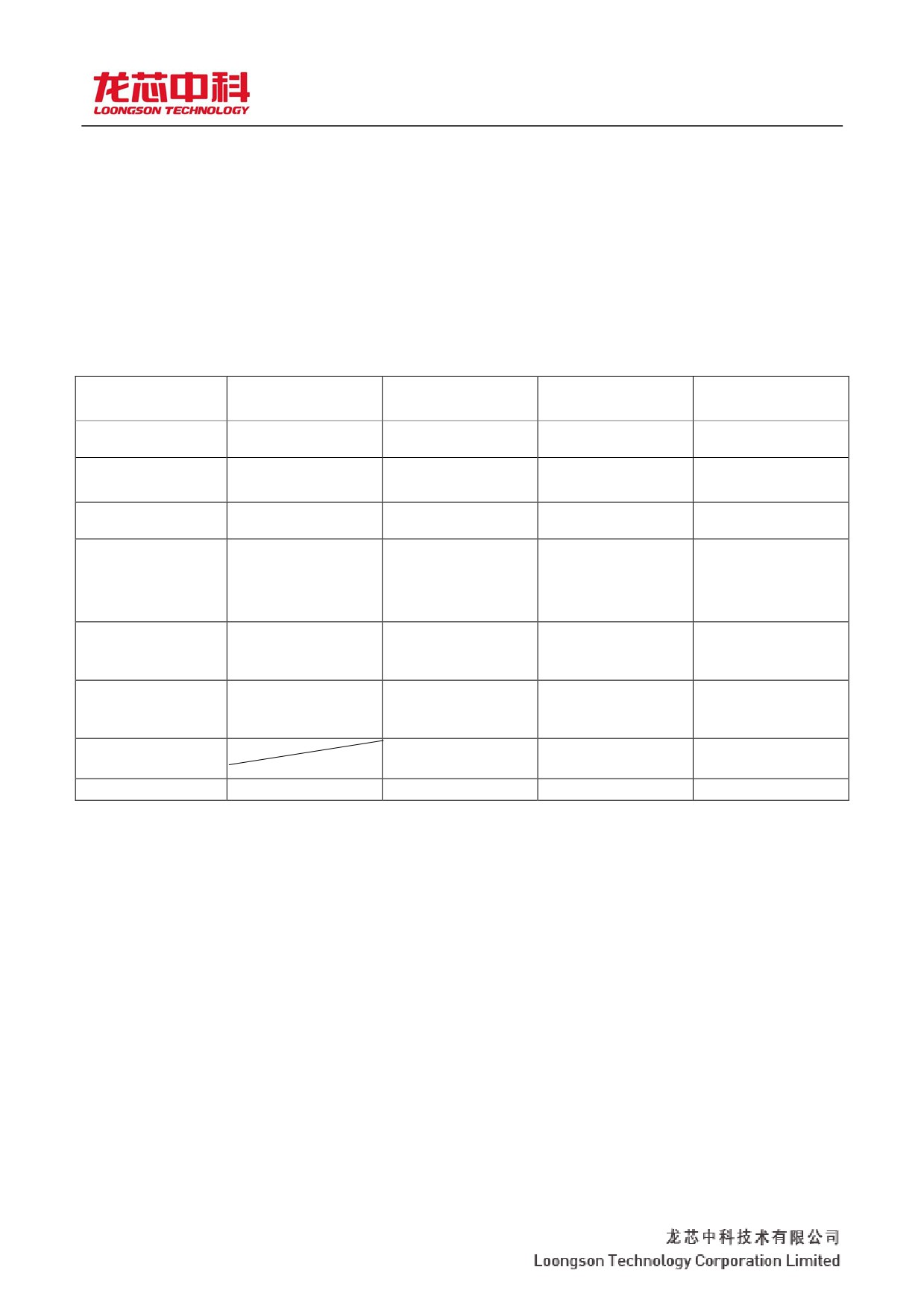
Table 5-1 lists some of the parameters for each cache.
Table 5-1 Cache parameters
Instruction
Data cache
Sacrifice the
Shared cache
cache
cache
capacity
64 KB
64 KB
256
2MB/ body (8MB in
KB
total)
Associative
4 road
4 road
16 road
16 road
degree
Line Size
512 - bit
512 - bit
512 -
512 - bit
bit
11 bits in a physical
The Index
Virtual
Virtual address
Virtual address
address
address ["]
["]
[13:6]
(Index)
See section 5.1.5 on
page 63
Label (Tag)
Physical
Physical address
Physical address
Physical address
address
[47:12]
[47:12]
[47:16]
[47:12]
Replacement
Random
LRU replacement
LRU replacement
LRU replacement
replacement
algorithm
algorithm
algorithm
strategy
algorithm
Write policy
Write back, write
Write back, write
Write back, write
assignment
assignment
assignment
Check way
parity
The SEC - DED ECC
The SEC - DED ECC
The SEC - DED ECC
5.1.2 Level 1 instruction Cache (I-cache)
The capacity of first-level instruction cache is 64KB, and 4-way group linkage structure is adopted. The
length of the data portion in each cached row is 64
A byte, divided into eight 8-byte wide blocks, is the smallest unit of data part access. The instruction cache
USES a virtual address index to the physical address label
The access mode of the visa. During access, the [13:6] bit of the virtual address is used as the index of the
cached row, the part below the 5th bit of the virtual address is used to Cache the inline index, and the part above the
14th bit of the virtual address is converted into a virtual and real address at the same time. The converted physical
address high bit is compared with the content read out by tags in each channel to determine whether the Cache is hit.
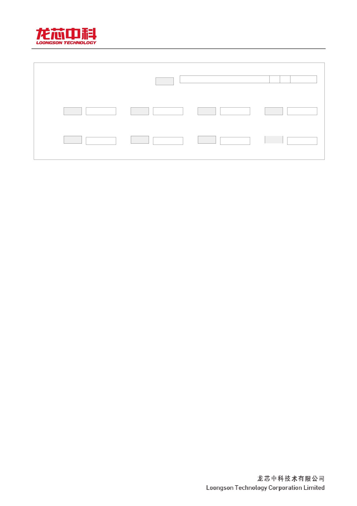
Figure 5-2 shows the structure of the instruction cache line. In addition to the high order (PTAG) of the physical
address, the Tag contains the significant bit (V) and information about which way the Cache row is located in the
S-cache (SCWAY). A significant bit of 1 means that the content on the cached row is meaningful, and no valid
content on the cached row of table 0.
61
龙芯 3A3000/3B3000 处理器用户手册 y 下册
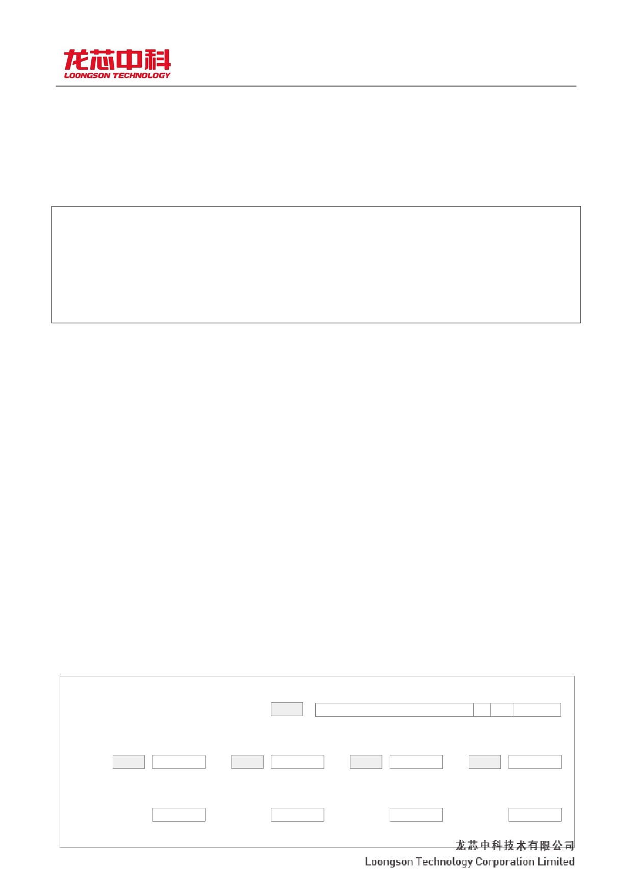
Figure 5-2 Shows the line structure of the level 1 instruction cache
7040
6 54 3
0
ptag
0
v
scway
The
ecc_t
8
36
1 b1b
4
6356, 511,
448
5548, 447,
384
4740, 383,
320
3932, 319,
256
ecc_d7
block7
ecc_d6
block6
ecc_d5
block5
ecc_d4
block4
8
64
8
64
8
64
8
64
The
3124, 255,
192
2316, 191,
128
158, 127,
64
7
0 63
0
ecc_d3
block3
ecc_d2
block2
ecc_d1
block1
ecc_d0
block0
8 b
64 b,
8 b
64 b,
8 b
64 b,
8 b
64
b,
The first-level instruction cache USES parity to check the Tag and Data parts in the cache line. When a new
cache line is updated into the instruction cache, the Data section takes blocks as the basic unit of validation. Each
block generates 8-bit validation results and records them. After the Tag section extends its 0 to 64 bits, the same
validation algorithm is used to generate 8-bit validation results and also records them. When the cache is read, the
raw data and the reference checksum are
62
龙芯 3A3000/3B3000 处理器用户手册 y 下册
At the same time, read out and recalculate the check value against the original data. If it is inconsistent with the
reference check value, it indicates a Cache error. The hardware will automatically invalidate the Cache line with the
error in i-cache and record relevant location information, triggering exceptions. If the software has no special
diagnostic needs, it can be returned directly from the exception handler, and when the processor resumes execution,
it will retrieve the required Cache line contents from V-Cache, S-cache, or memory. It should be noted that when
the software fills the instruction Cache with Store Tag and Store Data class Cache instructions, the parity value of
the contents must be calculated at the same time, and the errctL.ECC field must be explicitly stored. When the
Parity generation algorithm:
Function Parity_Gen(Datain, parityout) endfunction
Parity_Gen 63..07..0
Parity detection algorithm:
The function Parity_Check (newparity, refparity, error) 7..07..0
Endfunction Parity_Check
hardware executes such Cache instructions, the reference checksum written in the instruction Cache comes from the
errctl.ECC field rather than the hardware circuit's automatic checksum generation result. This mechanism is mainly
used to complete some special diagnosis. The pseudo-code of the algorithm for generating and detecting parity
values of instruction cache is described as follows:
5.1.3 Level 1 data Cache (D-Cache)
The capacity of the first-level data cache is
64KB, and the 4-way group linkage structure and LRU
replacement algorithm are adopted. The length of the data section in each cached row is
64 bytes, divided into eight 8-byte wide blocks, blocks are the smallest unit of data part access. The data
cache USES a virtual address index physically
The access mode of the address label. During access, the [13:6] bit of the virtual address is used as the index
of the cached row, the part below the 5th bit of the virtual address is used to Cache the inline index, and the part
above the 14th bit of the virtual address is converted into a virtual and real address at the same time. The converted
physical address high bit is compared with the content read out by tags in each channel to determine whether the
Cache is hit. Figure 5-3 shows the structure of the data cache rows. In addition to the high (PTAG) position of the
physical address, the Tag includes cached row state information (CS), dirty Tag bit (W), and the location of the
cached row in the S-cache (SCWAY). Cs =0 means the cache row is invalid; Cs =1 means that the cached rows
are in a Shared state; Cs =2 indicates that the cached row is in an exclusive state; Cs =3 is the reserved value. W
=1 indicates that there is recently written data on the cache row.
Figure 5-3 Shows the row structure of the level 1 data cache
7042
7 54 3 June
0
The
ecc_t
ptag
W.
cs
scway
8
36
1 b2b
4
6356, 511,
448
5548, 447,
384
4740, 383,
320
3932, 319,
256
ecc_d7
block7
ecc_d6
block6
ecc_d5
block5
ecc_d4
block4
8
64
8
64
8
64
8
64
The
3124, 255,
192
2316, 191,
128
158, 127,
64
7
0 63
0
63