Loongson 3A3000/3B3000 processor user manual. Part ii GS464E processor core V1.2 - page 6
龙芯 3A3000/3B3000 处理器用户手册 y 下册
Control register Cause's ExcCode field:
0x0a (RI) (see Table 7-28 on page 111)
Additional hardware status updates in
response to exceptions:
There is no
6.1.20 No exceptions can be made to the coprocessor
The triggering coprocessor is not an exception when:
z When not in debug mode or core mode and status.cu0 =0, execute COP0 class instruction
(opcode=0b010000), CACHE class instruction (opcode=0b101111), LWPTE, LWDIR, LDPTE, LDDIR.
z When status. CU1=0, execute COP1 instruction (opcode=0b010001), COP1X instruction
(opcode=0b010011), LWC1, SWC1, LDC1, SDC1, MOVF, MOVT, 64-bit multimedia instruction (Opcode
=0b010010, func= 0B000000 ~0b000011, RS = 11,000 ~11111; Opcode = 0 b010010, func b001000 = 0
~ 0 b001110,Rs = 11000 ~ 11101), gsLWLC1GsLWRC1, gsLDLC1, gsLDRC1, gsLWLEC1, gsLWGTC1,
gsLDLEC1, gsLWXC1, gsLWXC1, gsLDXC1, gsSWLC1, gsSWRC1, gsSDLC1, gsSDRC1, gsSWLEC1,
gsSWGTC1, gsSDLEC1, gsSDGTC1, gsSQC1, gsSWXC1, gsSWXC1.
z When status. CU2=0, COP2 instruction (opcode=0b010010), LWC2 instruction (opcode=0b110010),
SWC2 instruction (opcode=0b111010), LDC2 instruction (Opcode =0b110110), SDC2 instruction (Opcode
=0b111110) are executed.But does not includeSETMEM, gsLBLE, gsLBGT, gsLHGT, gsLHGT, gsLDLE,
gsLDGT, gsLQ, gsLBX, gsLHX, gsLWX, gsLDX, gsSBLE, gsSBGT, gsSHGT, gsSWGT, GSSSDLE,
gsSQ, gsSBX, gsSHX, gsSWX, gsSDX, LWPTE, LWDIR, LDPTE, LDDIR64 bit multimedia instruction
(Opcode =0b010010, func= 0B000000 ~ 0B000011, RS = 11,000 ~11111; Opcode = 0 b010010, func
b001000 = 0 ~ 0 b001110,Rs = 11,000 ~11101), gsLWLC1, gsLWRC1, gsLWRC1, GSLDLECc1,
gsLDLEC1, gsLDGTC1, gsLQC1, gsLWXC1, gsLDXC1, gsSWLC1, gsSWRC1, gsSDLC1, gsSDRC1,
gsSWLEC1, gsSWGTC1, gsSDLEC1, gsSWGTC1, gsSDLEC1, gsSDGTC1, gsSQC1, gsSWXC1,
gsSWXC1.
Note: in Guest mode, when guest.status. cu1/2 =1 but root.status. cu1/2 =0, the trigger coprocessor can't use the
exception to directly fall into Root mode.
Control register Cause's ExcCode field:
0x0b (CpU) (see Table 7-28 on page 111)
Additional hardware status updates in
response to exceptions:
register
Status
update
description
Cause
The CE domain records the unavailable coprocessor number.
6.1.21 Floating-point exception
The floating-point coprocessor fires the floating-point exception. See section 2.2.4 on page 16 for a detailed
introduction to the floating point exception. Some floating point exceptions can be shielded by configuring the
Enable field of the FCSR register, see section 2.2.3 on page 13 for details.
Control register Cause's ExcCode field:
0x0F (FPE) (see Table 7-28 on page
80
龙芯 3A3000/3B3000 处理器用户手册 y 下册
111) Additional hardware status updates
in response to exceptions:
81
龙芯 3A3000/3B3000 处理器用户手册 y 下册
register
Status
update
description
FCSR
The Cause and Flag fields record specific floating point exception type
information.
6.1.22 Floating point stack exception
The floating-point stack exception is triggered when the SETTAG instruction is executed if the contents of the
source operand do not meet the specified criteria. This exception can be handled in both root and guest modes.
Control register Cause's ExcCode field:
0X10 (GSExc) (see Table 7-28 on page
111) GSExcCode field for control register
GSCause:
0x00 (IS) (see Table 7-43 on page 131)
6.2 interrupt
The interrupts described in this section cover hardware interrupts, software interrupts, timer interrupts, and
performance counter overflow interrupts. Non-masking interrupts (NMI), although it contains the word interrupt in
its name, is neither controlled nor affected by the interrupt system described in this section, so it is treated as a
separate special exception -- the non-masking interrupt exception.
6.2.1 Requirements for interrupt response
The necessary conditions for a processor to respond to an interrupt are:
y Status.IE=1 indicates that global interrupt enabled is enabled.
y Debug.dm =0, indicating that you are not in Debug mode.
y Staus.ERL=0 and status. EXL=0 indicate that neither error nor exception is being processed.
y An interrupt is caused by an interrupt source that is not masked,
6.2.2 Interrupt mode
What is described in this section applies to both the root and the guest modes. When it comes to virtual
machine environments in guest mode, the "hardware" in the concept of "hardware interrupts" described in this
section does not necessarily mean physical hardware, but follows the naming conventions of the MIPS specification.
GS464E supports two interrupt modes: mode 1, compatible interrupt mode
In this mode, the processor supports 2 software interrupts (SW0~SW1), 6 hardware interrupts (HW0~HW5), 1
timer interrupt and 1
Total performance counter overflow interrupt. Where timer interrupts and performance counters interrupt
multiplexing HW5 hardware interrupts.
80
龙芯 3A3000/3B3000 处理器用户手册 y 下册
The interrupt source of software interrupt is the two digits cause. IP[1:0], which can only be triggered by the
software to write 1 of the bit cause. IP[1:0], and the software to write 0
Clean up.
The interrupt source of the timer interrupt is recorded in the cause.ti bit and is set to 1 by hardware when
Count[31:0] equals Compare[31:0]. The software can indirectly clear the interrupts of the cause.ti bit record by
writing the Compare register.
The interrupt source of the performance counter overflow interrupt is recorded in the cause. PCI bit. When the
performance counter value overflow (the 47th bit of the counter is 1), the hardware sets 1. The software can
indirectly clear the cause. PCI bit by writing 0 to the 47th bit of the relevant performance counter numerical register.
1
The actual effective number of performance counters in 1 GS464E is 48 bits.
81
龙芯 3A3000/3B3000 处理器用户手册 y 下册
The interrupt source of hardware interrupt comes from the processor, and the 6 interrupt input pins on the
processor interface are sampled by the hardware beat by beat. The software needs to reverse traverse the interrupt
routing path of the system to clear the interrupt state on the terminal device or routing path, so as to clear the
processor's hardware interrupt.
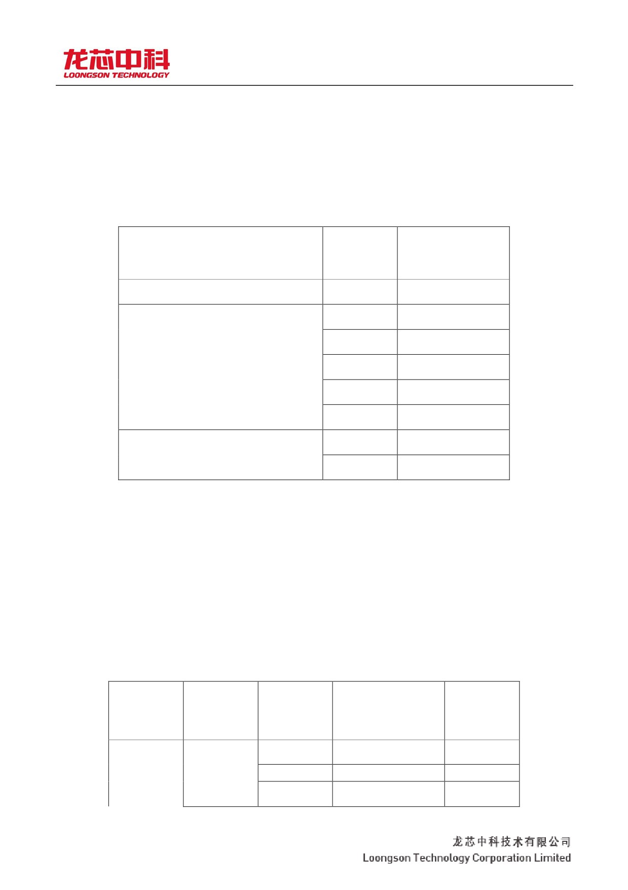
In addition to global interrupt enablement, each interrupt source contains an interrupt mask bit. The generation
relationships of each interrupt request are shown in Table 6-4.
Table 6-4 Generation of each interrupt request in compatible interrupt mode
Interrupt type
The
Interrupt request
interru
generation
pt
source
Hardware interrupt, timer interrupt, or
HW5
Cause. IP7 & Status.
performance counter overflow interrupt
IM7
Hardware interrupt
HW4
Cause. IP6 & Status.
IM6
HW3
Cause the IP5 & Status.
IM5
HW2
Cause. IP4 & Status.
IM4
HW1
Cause the IP3 & Status.
IM3
HW0
Cause. IP2 & Status.
IM2
Software interrupt
SW1
Cause. IP1 & Status.
IM1
SW0
Cause. IP0 & Status.
IM0
The same exception entry offset is used for all interrupts, whether the general exception entry offset (0x180) or
the special exception entry offset (0x200) is cause.IV determined. See Table 6-3 on page 72 for details.
The interrupt exception handler queries cause.ip and status.im to determine the specific interrupt source. In
the case of multiple effective interrupt sources, the priority of interrupt processing can be realized by adjusting the
order of the query.
Mode two, vector interrupt mode
This mode specifies a unique exception entry vector for each interrupt based on a compatible interrupt mode
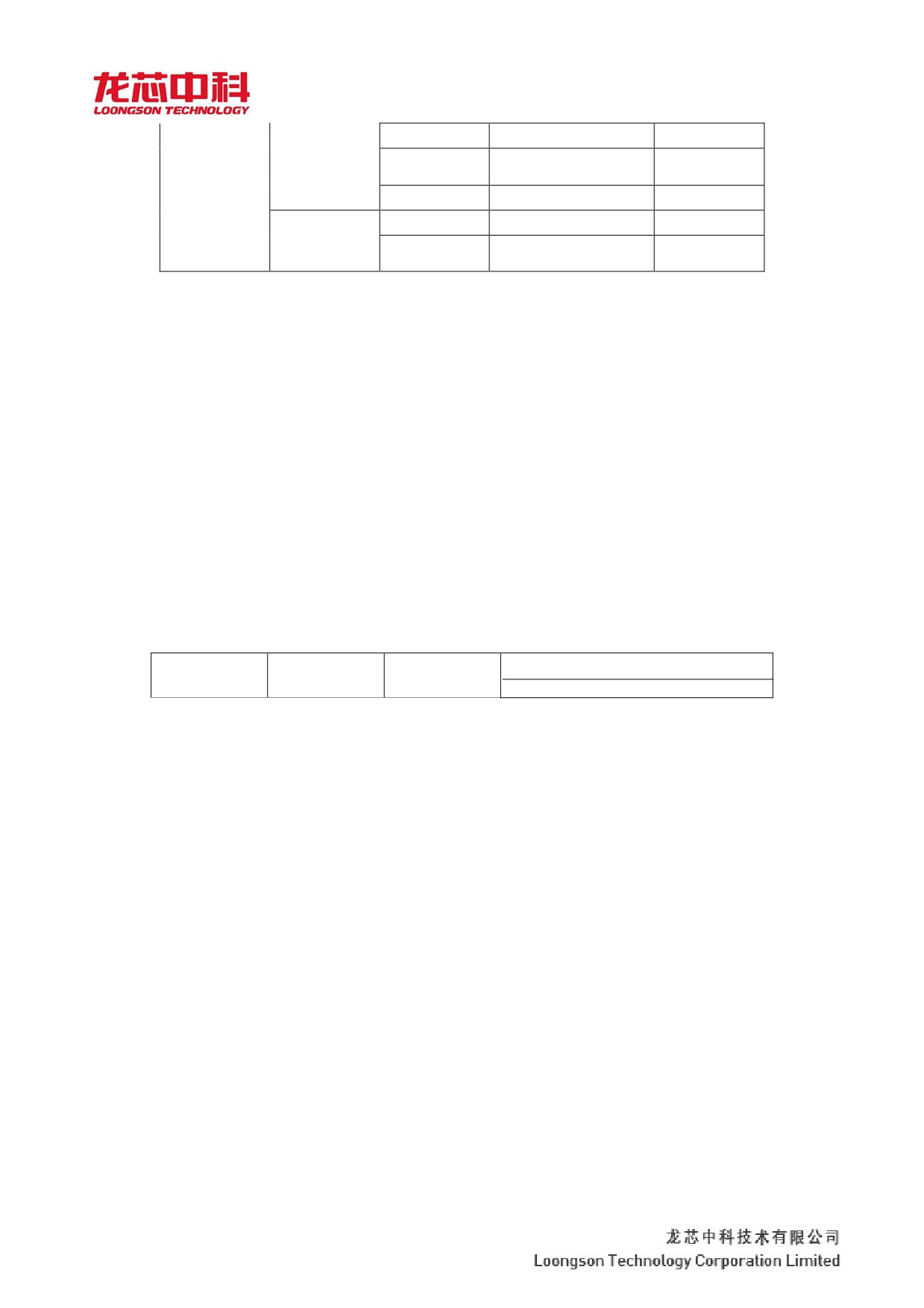
(see Table 6-3 on page 72 for calculation) and defines a fixed priority relationship for all interrupts, as shown in
Table 6-5.
Table 6-5 Priority relationship among interrupts in vector interrupt mode
priority
Interrupt
The
Interrupt request
Interrupt
type
interru
generation
vector
pt
number
source
Highest
Hardware
HW5
Cause. IP7 & Status. IM7
7
priority
interrupt
HW4
Cause. IP6 & Status. IM6
6
HW3
Cause the IP5 & Status.
5
IM5
82
龙芯 3A3000/3B3000 处理器用户手册 y 下册
HW2
Cause. IP4 & Status. IM4
4
HW1
Cause the IP3 & Status.
3
IM3
HW0
Cause. IP2 & Status. IM2
2
Software
SW1
Cause. IP1 & Status. IM1
1
interrupt
Lowest
SW0
Cause. IP0 & Status. IM0
0
priority
In vector interrupt mode, which hardware interrupt source the timer interrupts to reuse is defined by the
INTCTL.IPTI domain, see Table 7-25 on page 109. In vector interrupt mode, which hardware interrupt source the
performance counter overflows the interrupt multiplexes is defined by the INTCTL.ippCI field, see the table on
page 109
7 to 25.
GS464E does not implement shadow registers, so all interrupts in vector interrupt mode correspond to the same set of
logical general purpose registers (GPR).
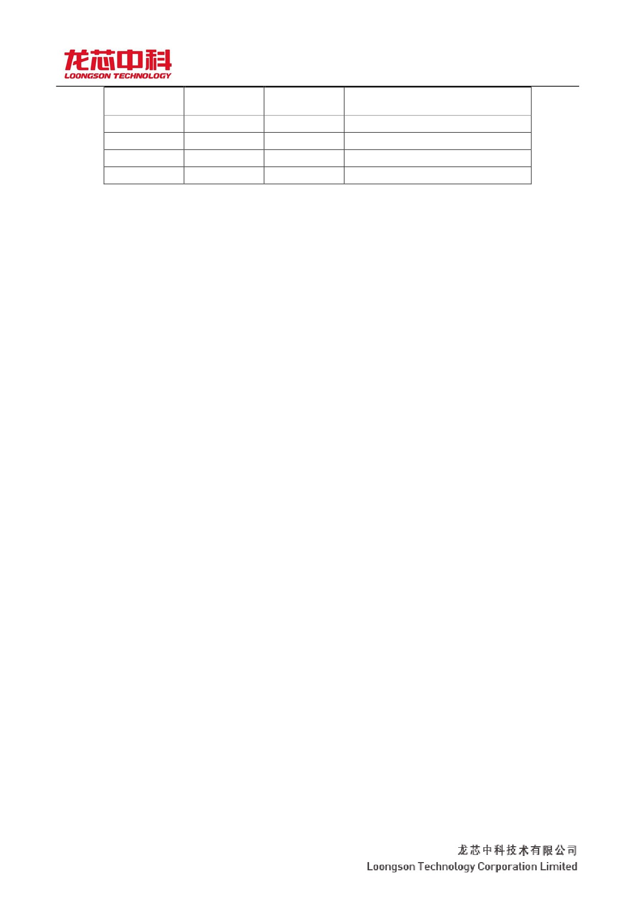
Which interrupt mode the processor currently adopts is determined by the status.bev, cause.IV, and INTctL.vs
domains. The corresponding relationship is shown in Table 6-6
Shown below.
Table 6-6 Interrupt mode determination
Status. BEV
Cause. IV
IntCtl. VS.
Interrup
t mode
83
龙芯 3A3000/3B3000 处理器用户手册 y 下册
Status. BEV
Cause. IV
IntCtl.
Interrupt
VS.
mode
1
The x1
x
Compatible interrupt mode
x
0
x
Compatible interrupt mode
x
x
= 0
Compatible interrupt mode
0
1
! = 0
Vector interrupt mode
6.2.3 Additional notes on interrupt handling
This manual only describes the structure and response mechanism of the interrupt system of GS464E. When
designing the loongson 3A3000 chip interrupt system, the software staff should refer to chapter 6 and 7 of
"Loongson 3A3000/3B3000 Processor Household Manual -- Volume I" at the same time.
The processor is only responsible for direct sampling and recording the external input high level hardware
interrupt request. It is not responsible for level conversion, nor is it responsible for extending the pulse interrupt
signal to the level signal. This work is done by the interrupt controller in the chip. See chapters 6 and 7 of the
Loongson 3A30000/3B3000 Processor User Manual, Vol. 1.
Depending on the signal behavior of the external hardware interrupt input, the interrupt request bits internally
connected directly to the external interrupt input (root.cause.ip [7:2] or gueve.cause.ip [7:2]) may change from 1 to
0 after the interrupt request is triggered and before the interrupt handler queries these request bits. Interrupt
handlers need to be able to handle this situation. It is recommended to return directly without doing any processing.
If special treatment is done for system diagnosis, please do not affect the normal behavior of the system.
For hardware interrupts directly affected by external hardware, the software usually needs to clear the interrupt
state of a terminal device. From the command sequence issued by the processor to clear interrupts, to the device
receiving the command to clear its interrupt state, to the level of the processor's interrupt input pin changing from 1
to 0
The process (interrupt input undo) may have an indefinite delay. If interrupt enablement is turned on
prematurely, the same interrupt may be re-sampled, a phenomenon known as "spurious interrupt". Software needs
to be able to handle this situation correctly. It is recommended that the software, after issuing a write command to
clear the device's interrupt state, explicitly read the interrupt state tag of the device concerned until the read status
tag has been cleared, and then fully enable the device's interrupt within the processor or on the interrupt routing
path. 2 The Longson 3A3000 chip has guaranteed that the delay of each interrupt source signal passing through the
interrupt routing path to the interrupt input pin of the processor is always less than the delay of the interrupt state
returning to the processor through the data access path. If "false interrupt" is still found during debugging, please
ask the software personnel to further inquire the data manual and user manual of the device chip and bridge
involved in the system.
84
龙芯 3A3000/3B3000 处理器用户手册 y 下册
1, x means it can be anything.
If the interrupt bit of the device is read-clear, the software needs to be careful when issuing query commands.
85
龙芯 3A3000/3B3000 处理器用户手册 y 下册
7 Coprocessor register 0
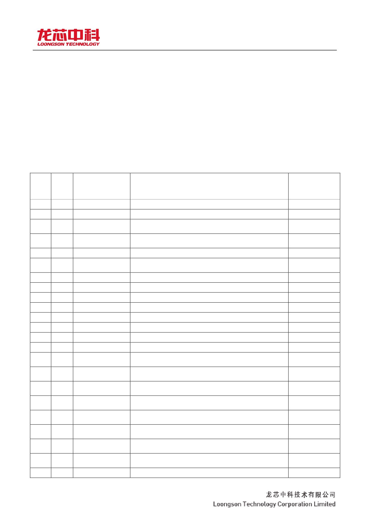
7.1 Root coprocessor 0 register overview
The coprocessor 0 register in the root mode context of the GS464E processor core is called the "root coprocessor 0 register"
The stores are listed
in Table 7-1.
Table 7-1 List of coprocessor 0 registers
Reg.
Sel.
Register name
Function
The
definiti
inde
on
x
0
0
The Index
VTLB accesses the specified index register with FTLB
Page 85, section 7.2
1
0
The Random
VTLB with FTLB access to random index registers
Page 86, section 7.3
2
0
EntryLo0
VTLB and FTLB table entry low order content associated with even
Page 87, section 7.4
number of virtual pages
3
0
EntryLo1
VTLB and FTLB table entry low order content related to odd
Page 87, section 7.4
number of virtual pages
4
0
The Context
A pointer to an in-memory page table entry
Page 90, section 7.5
4
2
UserLocal
Store user information that allows user-mode software to read
Page 91, section 7.6
through RDHWR commands
5
0
PageMask
VTLB page table size control
Page 92, section 7.7
5
1
PageGrain
1KB small pages and other page table property control
Page 93, section 7.8
5
5
PWBase
Page table base address register
Page 94, section 7.9
5
6
PWField
Configure the page table address index location for each level
Page 95, section 7.10
5
7
PWSize
Configure the page table pointer size for each level
Page 96, section 7.11
6
0
Wired
Control the number of fixed items in VTLB
Page 97, section 7.12
6
6
PWCtl
Control multilevel page table configuration
Page 98, section 7.13
7
0
HWRENa
RDHWR instruction access register enable control
Page 99, section 7.14
8
0
BadVAddr
Record the error address for the latest address-related exception
Page 100, section
7.15
9
0
The Count
Processor clock counter
Page 101, section
7.16
9
6
GSEBase
Loongson extension exception entry base address register
Page 102, section
7.17
9
7
PGD
Page table pointer register
Page 103, section
7.18
10
0
EntryHi
VTLB and FTLB table entries high content
Page 104, section
7.19
11
0
The Compare
Timer interrupt control
Page 106, section
7.20
12
0
The Status
Processor status and control registers
Page 107, section
7.21
12
1
IntCtl
Interrupts system state and control registers
Page 109, section
7.22
12
2
SRSCtl
Shadow register status and control register
Page 110, section
86
龙芯 3A3000/3B3000 处理器用户手册 y 下册
7.23
13
0
Cause
Store last exception reason
Page 111, section
7.24
14
0
The EPC
Store the PC on which the last exception instruction occurred
Page 113, section
7.25
15
0
PRId
The processor ID
Page 114, section
7.26
15
1
EBase
Exception entry base address register
Page 115, section
7.27
16
0
The Config
Configuration register
Page 116, section
7.28
16
1
Config1
Configure register 1
Page 117, section
7.29
16
2
Config2
Configure register 2
Page 118, section
7.30
87
龙芯 3A3000/3B3000 处理器用户手册 y 下册
Reg.
Sel.
Register name
Function
The
definition
inde
x
16
3
Config3
Configure Register 3
Page 119, section
7.31
16
4
Config4
Configure register 4
Page 121, section
7.32
16
5
Config5
Configure register 5
Page 123, section
7.33
16
6
GSConfig
Loong chip expansion configuration register
Page 124, section
7.34
17
0
LLAddr
Store the load-Link instruction access address
Page 127, section
7.35
20
0
XContext
Extended address mode next page table pointer
Page 128, section
7.36
22
0
Diag
The loong chip extended diagnostic control register
Page 129, section
7.37
22
1
GSCause
Store additional information about the last add-on exception
Page 131, section
7.38
23
0
The Debug
EJTAG Debug register
Page 133, section
7.40
24
0
DEPC
Holds the PC with the last EJTAG debug exception
Page 134, section
7.41
25
0 to 7
PerfCnt0 - PerfCnt7
Processor core internal performance counter access interface
Page 135, section
7.42
26
0
ErrCtl
Cache Parity/ECC Parity value register
Page 137, section
7.43
27
0
CacheErr
Cache Parity/ECC Parity status and control registers
Page 138, section
7.44
27
1
CacheErr1
Cache Parity/ECC Parity status with control register 1
Page 140, section
7.45
28
0
TagLo
The Cache Tag accesses the lower part of the interface
Page 141, section
7.46
28
1
DataLo
Cache Data access interface low part
Page 144, section
7.47
29
0
TagHi
Cache Tag access interface high part
Page 145, section
7.48
29
1
DataHi
Cache Data access interface high part
Page 146, section
7.49
30
0
ErrorEPC
The PC on which the last wrong instruction was stored
Page 147, section
7.50
31
0
DESAVE
EJTAG debug exception saves register
Page 148, section
7.51
31
2-7
KScratch1 - KScratch6
Core mentality accessible note registers 1~6
Page 149, section
7.52
88
龙芯 3A3000/3B3000 处理器用户手册 y 下册
7.2 Index Register (CP0 Register 0, Select 0)
The Index register is a 32-bit read-write register in which the Index information is used for TLBP, TLBR,
TLBWI instruction access
TLB.
Figure 7-1 illustrates the format of the Index register; Table 7-2 describes the Index register fields.
Figure 7-1 Index register format
31
30
11
10
0
P
0
The
Index
Table 7-2 Description of Index register field
Domain
positio
Functional
Read
Reset
name
n
descriptio
/writ
value
n
e
TLB queries failed flags. When the TLBP instruction fails to find a match in TLB, the
P
31
R
0 x0
position is 1;
Otherwise set to 0.
0
30.. 11
Read only is always 0.
0
0
TLB accesses the index. The field is configured by the software to instruct subsequent
TLBR or TLBWI instructions to read or write the specified item of the TLB.
When the TLBP instruction executes, if a match is found, the index value of the match is
stored in the field; When no match is found, the contents of the Index field of the Index
The Index
10.. 0
R/W
0 x0
register can be any value.
The Index value of 0.. 63 The number 0.. used to indicate VTLB. A total of 63.
The Index value of 64..
1087 is used to indicate FTLB. Where ((index-64) div 128) is
used to indicate which path to visit FTLB, and which path to visit is determined by the
value of ((index-64) mod 128). For example, when the Index value is 798, it indicates
access to item ((798-64) mod 128 = 94 of the path to ((798-64) div 128 = 5).
Programming tips:
The reasonable value range of the Index field is 0 ~ 1087. When the value of the Index field is written beyond this range,
the processor result will be uncertain.
85
龙芯 3A3000/3B3000 处理器用户手册 y 下册
7.3 Random Register (CP0 Register 1, Select 0)
The Random register is a read-only register that holds the index value of TLBWR instruction access to TLB.
The index value stored in the Random register changes every clock cycle. The upper bound (including) of the value
change is 63, and the lower bound (including) of the value change is the value set in the Wired register. The
Random register will automatically Reset to the upper bound when the Reset exception occurs and the Wired
register is written, i.e. 63.
When the value of the page size represented in the PageMask register is inconsistent with the page size
configured in the FTLB, the TLBWR instruction will operate only on THE VTLB, with the value in the current
Random register determining which entry is written to the VTLB.
The TLBWR instruction will operate only when the value of the page size represented in the PageMask
register is the same as the page size configured in FTLB
FTLB, which routing processor writes to FTLB is internally randomly determined, not using the contents of
the Random register. Figure 7-2 illustrates the format of the Random register; Table 7-3 describes each field of the
Random register.
Figure 7-2 Random register format
31
6
5
0
0
The
Random
Table 7-3 Description of Random register field
Domain
posit
Functional
Read
Reset
name
ion
descriptio
/writ
value
n
e
0
31.. 6
Read only is always 0.
0
0
The
5.. 0
The random index value written by VTLB.
R
0 x3f
Random
86
龙芯 3A3000/3B3000 处理器用户手册 y 下册
7.4 EntryLo0 and EntryLo1 registers (CP0 Register 2 and 3, Select 0)
The EntryLo0 and EntryLo1 registers serve as interfaces for TLBP, TLBR, TLBWI, and TLBWR instructions
to access the TLB, where EntryLo0 is used
The EntryLo1 register holds information for odd pages.
The EntryLo0 and EntryLo1 registers present a different format when accessed using DMFC0/DMTC0 and
MFC0/MTC0 instructions.
Figure 7-3 illustrates the format of the EntryLo0 and EntryLo1 registers when accessed by DMFC0/DMTC0
instructions; Table 7-4 describes the register fields in this case.
Figure 7-3 Register formats for EntryLo0 and EntryLo1 when accessed by DMFC0/DMTC0
instructions
63
62
61
60
42
41
32
RI
XI
K.
0
PFNX
31
30
29
6
5
4
3
2
1
0
PFNX
PFN
C
D
V
G
Table 7-4 Description of the register fields of EntryLo0 and EntryLo1 for DMFC0/DMTC0
instruction access
Domain
positio
Functional
Read
Reset
name
n
descriptio
/writ
value
n
e
Read prevents identifying bits. When the RI position of a TLB table entry is 1, the
processor fires an exception when an access instruction attempts to read on the page.
RI
63
Depending on the PageGrain register IEC field, the triggered exception could be a TLBL
R/W
0 x0
invalid exception or a TLBRI exception.
The XI fields of EntryLo0 and EntryLo1 can only be written if PageGrain=1. RIE
PageGrain = 0 RIE
, the RI fields of EntryLo0 and EntryLo1 will be read to 0 regardless of the value to be
written.
Execution block identification bits. When the XI position of a TLB table entry is 1, the
occurrence on the page is indicated and the processor fires the exception. Depending
XI
62
on the PageGrain register IEC field, the triggered exception could be a TLBL invalid
R/W
0 x0
exception or a TLBXI exception.
The XI fields of EntryLo0 and EntryLo1 can only be written if PageGrain=1. XIE
PageGrain = 0 XIE
, the XI fields of EntryLo0 and EntryLo1 will be read to 0 regardless of the value to be
written.
87
龙芯 3A3000/3B3000 处理器用户手册 y 下册
The kernel executes protection bits. If the processor is in kernel mentality, the processor will trigger
the TLB Invalid exception by pointing to the page K=0.
K.
61
R/W
0 x0
The K fields for EntryLo0 and EntryLo1 can only be written if gsconfig. KE=1.
GSConfig. KE = 0
, the K fields for EntryLo0 and EntryLo1 will be read to 0 regardless of the value to be
written.
0
60.. 42
Read only is always 0.
0
0
Physical page number extension. When the processor is configured to support the large physical
address space pattern (Config3=1 and PageGrain=1), the domain contents are splicedto the high
order of the PFN domain to form a complete physical page number, thus supporting the 48-bit
PFNX
41.. 30
R/W
0 x0
physical address space. LPAELPA The PFNX domain corresponds to the 47.. of the physical
address.
36.
If the processor is configured to not support the large physical address space pattern
(PageGrain=0), the PFNX field will ELPA1
Cannot write and reads return 0. Thus achieving compatibility with system software written based
on Release 1 of the MIPS specification.
1. The Config in the godson 3A1500 chip is always 1, so it is impossible to turn off the large physical address space mode support because of Config=0.
LPALPA
88
龙芯 3A3000/3B3000 处理器用户手册 y 下册
Domain
positi
Functiona
Read
Reset
name
on
l
/wri
value
descripti
te
on
Basic section of physical page number. When the processor is configured to support the large
physical address space pattern (Config3=1 and PageGrain=1), the field contents are splicedinto the
PFN
29.. 6
lower part of the PFNX field to form a complete physical page number, thus supporting the 48-bit
R/W
0 x0
physical address space. LPAELPA The PFN domain corresponds to 35.. of the physical
address.
12.
When the processor is configured to not support a large physical address space pattern
(PageGrain=0), the PFN field itself ELPA
The final physical page number is formed to support the 36-bit physical address space.
The Cache property of the physical page. See this section for a detailed definition of the
C
5.. 3
R/W
0 x0
Cache property and its encoding
That's shown in table 7 minus 6.
Dirty bits. When the dirty position in the page table is 1, the page can be written;
D
2
R/W
0 x0
Otherwise for a dirty location it is 0
The TLB Mod exception will be triggered if the page of.
Significant bit. When the valid position in the page table is 1, it means that the page is
V
1
R/W
0 x0
accessible; Otherwise access a valid location
A page of 0 would trigger the TLB Invalid exception.
The global level. When a page table entry is filled into a TLB, the EntryLo0 and
EntryLo1 register's two G-bit values are logically matched, resulting in the global
G
0
identity bit for the page table entry. When the global identity bit in the page table is 1, asids are
R/W
0 x0
not compared in the TLB address match lookup.
When page table entries are read from TLB, both G bits of the EntryLo0 and EntryLo1
registers reflect both reads
G bit information for page table entries.
Figure 7-4 illustrates the format of the EntryLo0 and EntryLo1 registers when accessed by the MFC0/MTC0
instructions; Table 7-5 describes the register fields in this case. Note that the KE bit of the page table cannot be
accessed at this time. The KE bit of the TLB table entry will be written to the default value 0.
Figure 7-4 Register formats for EntryLo0 and EntryLo1 when accessed by MFC0/MTC0 instructions
63
32
SignExt
31
30
29
6
5
4
3
2
1
0
RI
XI
PFN
C
D
V
G
Table 7-5 Description of the register fields for EntryLo0 and EntryLo1 at MFC0/MTC0
instruction access
Domain
positi
Functiona
Read
Reset
name
on
l
/wri
value
descripti
te
88
龙芯 3A3000/3B3000 处理器用户手册 y 下册
on
When MTC0 is used to write, the contents corresponding to this part in the register are
SignExt
63.. 32
R
0 x0
ignored and the PFNX field is written 0.
When MFC0 is read out, this part of the contents returned to the general purpose register
is extended by the RI bit symbol.
Read prevents identifying bits. When the RI position of a TLB table entry is 1, the
processor fires an exception when an access instruction attempts to read on the page.
RI
31
Depending on the PageGrain register IEC field, the triggered exception could be a TLBL
R/W
0 x0
invalid exception or a TLBRI exception.
The XI fields of EntryLo0 and EntryLo1 can only be written if PageGrain=1. RIE
PageGrain = 0 RIE
, the RI fields of EntryLo0 and EntryLo1 will be read to 0 regardless of the value to be
written.
89
龙芯 3A3000/3B3000 处理器用户手册 y 下册
Domain
positio
Functional
Read
Reset
name
n
descriptio
/writ
value
n
e
Execution block identification bits. When the XI position of a TLB table entry is 1, the
occurrence on the page is indicated and the processor fires the exception. Depending
XI
30
on the PageGrain register IEC field, the triggered exception could be a TLBL invalid
R/W
0 x0
exception or a TLBXI exception.
The XI fields of EntryLo0 and EntryLo1 can only be written if PageGrain=1. XIE
PageGrain = 0 XIE
, the XI fields of EntryLo0 and EntryLo1 will be read to 0 regardless of the value to be
written.
Basic section of physical page number. When the processor is configured to support the large
physical address space pattern (Config3=1 and PageGrain=1), the field contents are splicedinto the
PFN
29.. 6
lower part of the PFNX field to form a complete physical page number, thus supporting the 48-bit
R/W
0 x0
physical address space. LPAELPA The PFN domain corresponds to 35.. of the physical
address.
12.
When the processor is configured to not support a large physical address space pattern
(PageGrain=0), the PFN field itself ELPA
The final physical page number is formed to support the 36-bit physical address space.
The Cache property of the physical page. See this section for a detailed definition of the
C
5.. 3
R/W
0 x0
Cache property and its encoding
That's shown in table 7 minus 6.
Dirty bits. When the dirty position in the page table is 1, the page can be written;
D
2
R/W
0 x0
Otherwise for a dirty location it is 0
The TLB Mod exception will be triggered if the page of.
Significant bit. When the valid position in the page table is 1, it means that the page is
V
1
R/W
0 x0
accessible; Otherwise access a valid location
A page of 0 would trigger the TLB Invalid exception.
The global level. When a page table entry is filled into a TLB, the EntryLo0 and
EntryLo1 register's two G-bit values are logically matched, resulting in the global
G
0
identity bit for the page table entry. When the global identity bit in the page table is 1, asids are
R/W
0 x0
not compared in the TLB address match lookup.
When page table entries are read from TLB, both G bits of the EntryLo0 and EntryLo1
registers reflect both reads
G bit information for page table entries.
Programming tips:
Before any field contents of the PageGrain register are modified, the PFNX and PFN fields in the EntryLo0 and EntryLo1
registers must be written to 0, and all TLBS must be cleared. All the above operations must be done in the
Unmapped Address Space. If you do not follow the instructions here, the processor behavior
is uncertain.
Table 7-6 Cache attribute encoding table
Page table C
Cache
domain
attribute 1
encoding
0
Reserve, forced configuration will cause a crash
1
Reserve, forced configuration will cause a crash
90
龙芯 3A3000/3B3000 处理器用户手册 y 下册
2
Uncached
3
Cached
4
Reserve, forcing the configuration is equivalent to Cached
5
Reserve, forcing the configuration is equivalent to Cached
6
Reserved, forced configuration will access the EJTAG Dseg
space, there is a risk of crash
7
Uncached Accelerated
1 For definitions of the Uncached, Cacheable, and Uncached Accelerated properties, see section 5.2 on page 60.
91
龙芯 3A3000/3B3000 处理器用户手册 y 下册
7.5 Context Register (CP0 Register 4, Select 0)
The Context register is a read-write register that contains some page-table base address high level information
filled in by the operating system software and some bits of the error virtual address with the TLB exception.
According to the original design intent of the MIPS architecture, the information splited together in the Context
register can form a pointer to an item in the page table, which can be accessed when a TLB exception occurs. The
page table that can be accessed without any processing of the contents in the Context register is a single-level page
table structure. The page size is 4K bytes, and each page table item is 16 bytes. It contains an even page table item
and an odd page table item with consecutive virtual address, totaling 512K odd and even page table items. When
the page table does not adopt this structure, the software needs to properly shift and concatenate the contents of the
Context register. For an operating system with multilevel page tables, the Context register can only be used to
speed up address generation for the last level of page table access.
The Context register is primarily used in the TLB Refill exception handler. But when exceptions such as
XTLB Refill, TLB Invalid, and TLB Mod occur, the BadVPN2 domain in the Context register is also updated, so
the software can also use the Context register in the corresponding exception handler.
The BadVPN2 domain in the Context register copies some of the information in the BadVAddr register, but
this does not mean that this part is completely equivalent. When the Address Error exception occurs, the BadVaddr
register is updated by the hardware, but the BadVPN2 domain of the Context register is not updated by the
hardware.
Figure 7-5 illustrates the format of the Context register; Table 7-7 describes the fields of the Context register.
Figure 7-5 Context register format
63
32
PTEBase
31
23
22
21
20
19
18
17
16
15
14
13
12
11
10
9
8
7
6
5
4
3
2
1
0
PTEBase
BadVPN2
0
Table 7-7 Description of the Context register fields
Domain
positio
Functional
Read
Reset
name
n
descriptio
/writ
value
n
e
PTEBase
63.. 23
Page table base address high level. Configured by the operating system software according R/W
There is no
to the current page table.
BadVPN2
22.. 4
When a TLB exception occurs, store the error virtual address of 31.. 13.
R
There is no
0
3.. 0
Read only is always 0.
0
0
90
龙芯 3A3000/3B3000 处理器用户手册 y 下册
7.6 UserLocal Register (CP0 Register 4, Selelct 2)
The UserLocal register is a read-write register that is not used to control the processor's hardware and is not
changed by the hardware.
The contents of the UserLocal can be read in user mode via the RDHWR instruction, and whether it can be
read is controlled by the HWRENCH a register bit 29. Figure 7-6 illustrates the format of the UserLocal register;
Table 7-8 describes the UserLocal register fields.
Figure 7-6 UserLocal register format
63
0
UserInformation
Table 7-8 Description of UserLocal register fields
Domain
positi
Functiona
Read
Reset
name
on
l
/wri
value
descripti
te
on
UserInfor
63.. 0
The information stored is not affected by or affected by the processor
R/W
There is
- mation
hardware.
no
91
龙芯 3A3000/3B3000 处理器用户手册 y 下册
7.7 PageMask Register (CP0 Register 5, Select 0)
The PageMask register is a read-write register, used in the process of reading and writing TLB; It contains a
comparison mask for each TLB
Table entries set different page sizes.
Figure 7-7 illustrates the format of the PageMask register; The PageMask register fields are described in
Table 7-9.
Figure 7-7 PageMask register format
6332
0
31
30
13
12
11
10
0
0
Mask
MaskX
0
Table 7-9 PageMask register field description
Domain
positio
Functional
Read
Reset
name
n
descriptio
/writ
value
n
e
0
63.. 31
Read only is always 0.
0
0
When translating between real and virtual addresses, each bit in the Mask field [17:0] is
Mask
30.. 13
used to indicate whether the corresponding bit in the virtual address [30:13] bit is
R/W
0 x3
compared. 1: No comparison; 0: Compare.
See Table 7-10 below for the Mask codes supported by longson and their corresponding
page sizes.
MaskX
12.. 11
Constant 3, 1KB pages are not supported.
R
0 x3
0
10.. 0
Read only is always 0.
0
0
Table 7-10 shows the Mask domain codes supported by GS464E and their corresponding page sizes.
Table 7-10 Mask domain codes and page sizes
Mask encoding
Page size
0 x0
4 KB
0 x3
16 KB
0 xf
64 KB
0 x3f
256 KB
0 XFF
1 MB
0 x3ff
4 MB
0 XFFF
16
MB
0 x3fff
64
MB
0 XFFFF
256 MB
92
龙芯 3A3000/3B3000 处理器用户手册 y 下册
0 x3ffff
1 gb
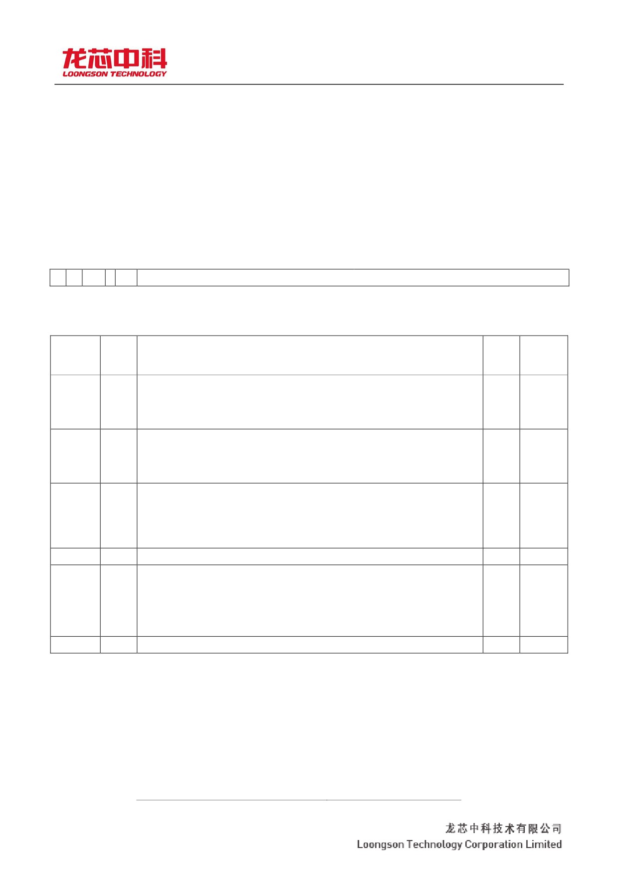
Programming tips:
Although GS464E allows the PageMask registers to be filled in: 0x1, 0x7, 0x1F, 0x7F, 0x1FF, 0x7FF,
0x1FFF, 0x7FFF,
0x1FFFF, the page size is 2KB (n=0.. 2n+1 8), but the processor does not guarantee the correctness of the program running under
this configuration.
93
龙芯 3A3000/3B3000 处理器用户手册 y 下册
7.8 PageGrain Register (CP0 Register 5, Select 1)
The PageGrain register is a read-write register. The GS464E implements only the parts of it that are related to
the TLB XI/RI protection bit and large physical address pattern control.
Figure 7-8 illustrates the format of the PageGrain register; The fields of the PageGrain register are described
in Table 7-11.
Figure 7-8 PageGrain register format
31
30
29
28
27
26
0
RIE
XIEELPA
IEC
0
Table 7-11 Description of PageGrain register field
Domain
positio
Functional
Read
Reset
name
n
descriptio
/writ
value
n
e
When I made a detour to the TLB wedge, I stopped in to make a functional detour.
RIE
31
0: Turn off the function. The RI bits of the EntryLo0 and EntryLo1 registers will disable
R/W
0 x0
writing and force them to be 0;
1: Enable this function. RI bits of the EntryLo0 and EntryLo1 registers work fine.
When I stopped in to the TLB short wedge function, I made a short detour.
XIE
30
0: Turn off the function. The XI bits of the EntryLo0 and EntryLo1 registers are disabled
R/W
0 x0
and forced to be 0;
1: Enable this function. The XI bits of the EntryLo0 and EntryLo1 registers work fine.
Large physical address function enablement bit.
ELPA
29
0: Turn off the function. The PFNX fields of the EntryLo0 and EntryLo1 registers disable
R/W
0 x0
writing and force 0;
1: Enable this function. The PFNX fields for the EntryLo0 and EntryLo1 registers work
fine.
0
28
Read only is always 0.
0
0
TLB reads block and performs block exception encoding and entry control bits.
0: TLB read block and execute block exception encoding and entrance multiplexing TLBL
IEC
27
R/W
0 x0
exception encoding and entrance;
1: TLB read block exception USES TLBRI exception encoding and entry, TLB performs
block exception USES TLBXI exception encoding and entry.
0
26.. 0
Read only is always 0.
0
0
Programming tips:
Before the software attempts to modify PageGrain any fields, all TLBS must be cleared and the fields of the
COP0 register listed below must be set to the specified value, otherwise the behavior of the processor will be
uncertain.
COP0 register field
Specif
y a
value
94
龙芯 3A3000/3B3000 处理器用户手册 y 下册
EntryLo0PFN, EntryLo1PFN
0
EntryLo0PFNX, EntryLo1PFNX
0
95
龙芯 3A3000/3B3000 处理器用户手册 y 下册
7.9 PWBase Register (CP0 Register 5, Select 5)
The PWBase register is a 64-bit read-write register that holds the virtual address of the page table base address.
This register is used in conjunction with the PWField, PWSize, and PWCtl registers and is used in GS464E to
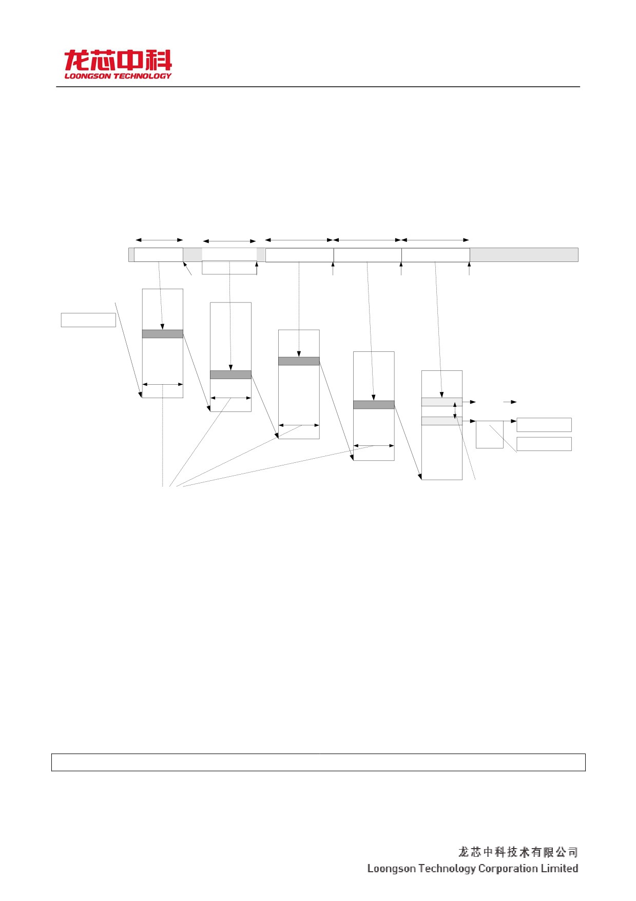
provide configuration information for the execution of the LDDIR and LDPTE directives. The LDDIR and LDPTE
directives support traversal lookup of multilevel page table structure, which can contain up to four levels of catalog
tables and one level of page table entries. The supported page table structure is shown in Figure 7-9.
Figure 7-9 Page table access procedures supported by PWBase,PWField,PWSize and PWCtl
PWSizePWSize BDW GDW
PWSizePWSizePWSize UDW MDW
PTW
Address
Bindex
Uindex
Mindex
PTindex
to look up
Gindex
BadVAddr
PWField BDI
PWField
PWFieldPWFieldPWField UDI MDI
PTI
GDI
PWBase
EntryLo0
Base address directory table
>>
EntryLo1
Global table of contents
32 b
32 b
/ 64
/ 64
32
b
Upper
b?
b?
or
PWField
64 b?
32
table of
b
PTEI
Intermedia
Or
contents
64 b?
te
directory
table
PWSize PTE
Page table table
PWSize PS
Figure 7-10 illustrates the format of the PWBase register; Table 7-12 describes the PWBase
register fields.
Figure 7-10. PWBase register format
63
0
PWBase
Table 7-12 Description of the PWBase register fields
96
Domain
positio
Functional
Read
Reset
name
n
descriptio
/writ
value
n
龙芯 3A3000/3B3000 处理器用户手e册
y 下册
PWBase
63.. 0
Page table base address.
R/W
0 x0
97
龙芯 3A3000/3B3000 处理器用户手册 y 下册
7.10 PWField Register (CP0 Register 5, Select 6)
The PWField register is used in conjunction with the PWBase, PWSize, and PWCtl registers in GS464E to
provide configuration information for the execution of the LDDIR and LDPTE directives. The LDDIR and LDPTE
directives support traversal lookup of multilevel page table structure, which can contain up to four levels of catalog
tables and one level of page table entries. See Figure 7-9 on page 94 for the supported page table structure and
access procedure. The index value of each level page table to the next level page table or the final page table entry
is obtained by intercepting part of the contiguous bit from the virtual address to be looked up (BadVAddr). The
PWField register is used to identify the starting point of the page table index truncated in the pending virtual
address (BadVAddr).
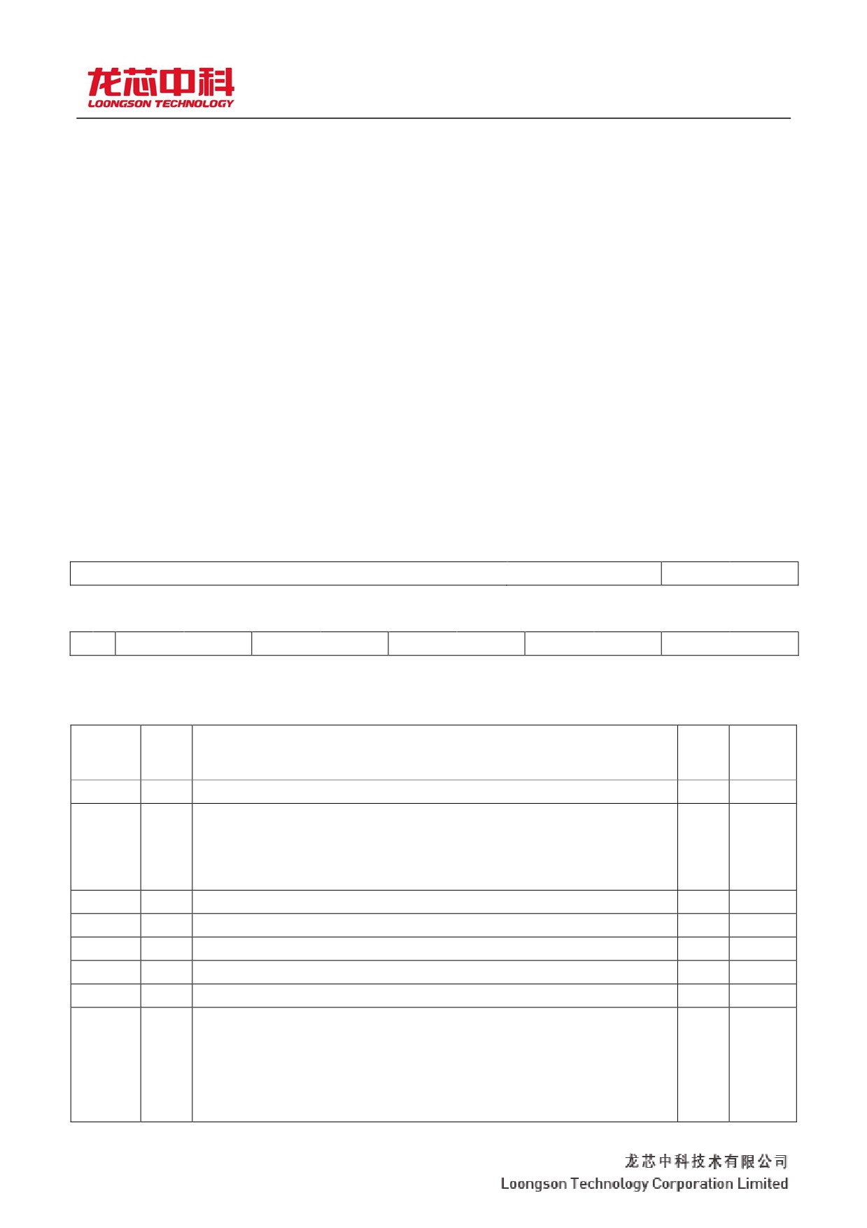
Figure 7-11 illustrates the format of the PWField register; Table 7-13 describes the PWField
register fields.
Figure 7-11. PWField register format
63
38
37
32
0
BDI
31
30
29
24
23
18
17
12
11
6
5
0
0
GDI
UDI
MDI
PTI
PTEI
Table 7-13 Description of PWField register fields
Domain
positio
Functional
Read
Reset
name
n
descriptio
/writ
value
n
e
0
63.. 38
Read only is always 0.
0
0
The Base Directory starts the index.
BDI
37.. 32
The use of the base directory table is controlled by the PWCtl. PWDirExt The base directory
R/W
0 x0
table can be used to distinguish between different page tables, such as the user page table and the kernel
page table, which can be maintained separately.
0
31.. 30
Read only is always 0.
0
0
GDI
29.. 24
Global Directory index starting position.
R/W
0 x0
UDI
23.. 18
The Upper Directory starts the index.
R/W
0 x0
MDI
17.. 12
MIddle Directory is the starting point of an index.
R/W
0 x0
PTI
11.. 6
Page Table index starting position.
R/W
0 x0
Page table item shift amount.
The content of the page table entry read out will be logically shifted to the right pTEI-2 bit
PTEI
5.. 0
to remove the information in the page table entry that is only used for software and does
R/W
0 x0
not need to be put into TLB. The loop is then rotated 2 bits to the right to move the RI and
XI two-bit information to either the highest two bits of EntryLo0 or EntryLo1. Therefore,
98
龙芯 3A3000/3B3000 处理器用户手册 y 下册
the PTEI field cannot be filled with 0 or 1, otherwise the processor result will be indeterminate.
99
龙芯 3A3000/3B3000 处理器用户手册 y 下册
7.11 PWSize Register 5, Select 6
The PWSize registers are used in conjunction with the PWBase, PWField, and PWCtl registers and are used in
GS464E to provide configuration information for the execution of the LDDIR and LDPTE directives. The LDDIR
and LDPTE directives support traversal lookup of multilevel page table structure, which can contain up to four
levels of catalog tables and one level of page table entries. See Figure 7-9 on page 94 for the supported page table
structure and access procedure. The index value of each level page table to the next level page table or the final
page table entry is obtained by intercepting part of the contiguous bit from the virtual address to be looked up
(BadVAddr). The PWSize register is used to identify the number of contiguous bits intercepted by the page table
index at each level in the virtual address to be looked up (BadVAddr).
The PWSize field is used to control whether the bit width of the pointer in the directory table is 32 or 64 bits.
PS The index value taken from the virtual address to be looked up (BadVAddr) by the various table of contents
according to PWField and PWSize needs to be multiplied by the width of the pointer in the table of contents
(moved 2 bits left or moved 3 bits left) to form a true access address. Only 64-bit Pointers can be used in the
XTLB Refill exception and 32-bit or 64-bit Pointers can be used in the TLB Refill exception.
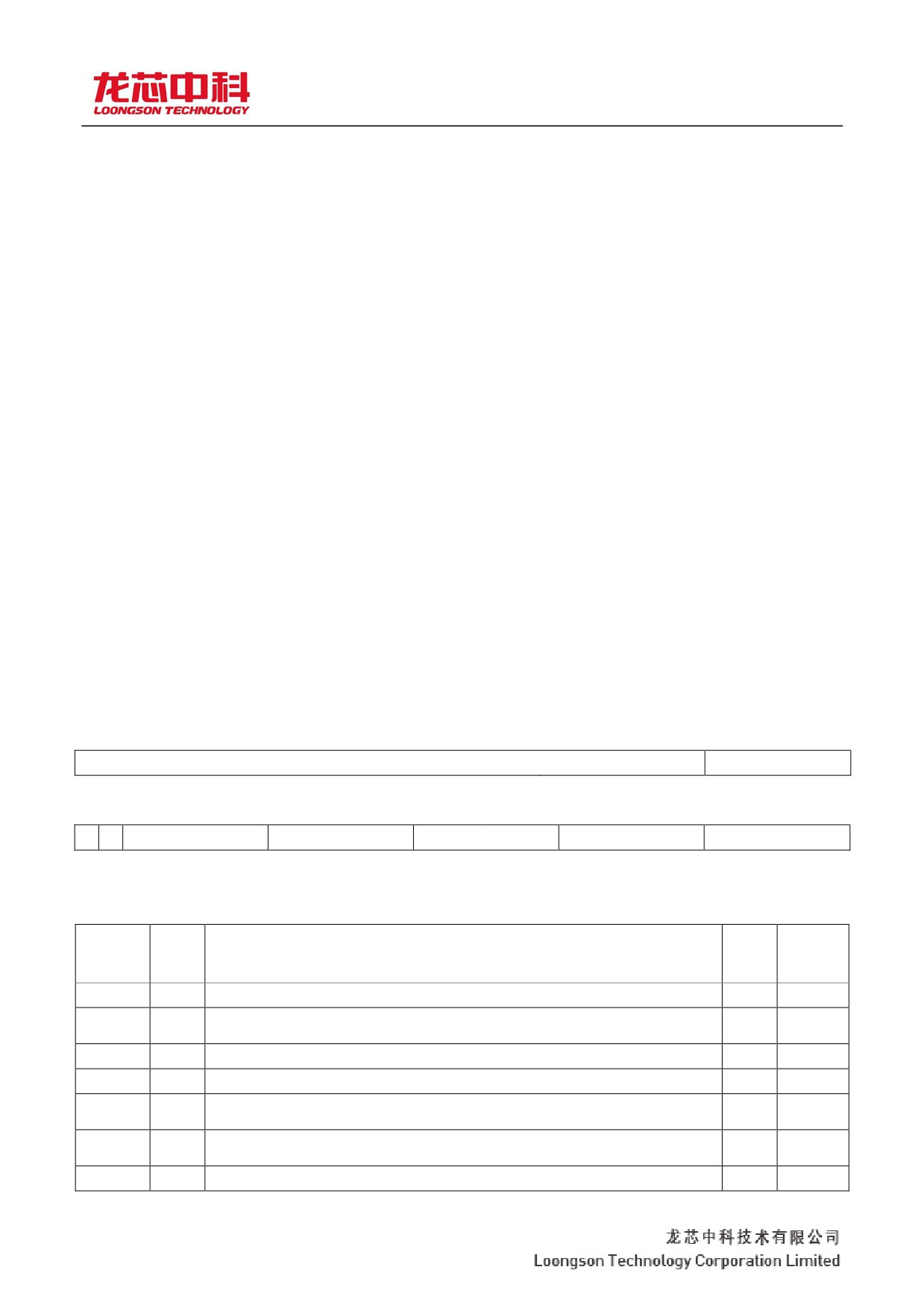
Figure 7-12 illustrates the format of the PWField register; Table 7-13 describes the PWField
register fields.
Figure 7-12. PWSize register format
63
38
37
32
0
BDW
31
30
29
24
23
18
17
12
11
6
5
0
0
PS
GDW
UDW
MDW
PTW
PTEW
Table 7-14 Description of the PWSize register fields
Domain
positio
Functional
Read
Reset
name
n
descriptio
/writ
value
n
e
0
63.. 38
Read only is always 0.
0
0
BDW
37.. 32
Base directory table index bit width. A value of 0 means that the base address directory
R/W
0 x0
table does not need to be looked up.
0
31
Read only is always 0.
0
0
PS
30
Level directory table pointer bit width. 0:32 pointer; 1:64 pointer.
R/W
0 x0
GDW
29.. 24
Global directory table index bit width. 0 is meaningless and the processor result is
R/W
0 x0
uncertain when configured as 0.
UDW
23.. 18
Upper directory table index bit width. 0 is meaningless and the processor result is
R/W
0 x0
uncertain when configured as 0.
MDW
17.. 12
Intermediate directory table index bit width. 0 is meaningless and the processor result is
R/W
0 x0
100