Loongson 1C300 Processor User Manual (Version 1.0, 2014) - page 5
1111: 15.28ȝs (Binary Rollover), 32.77ȝs (Digital
Rollover)
11.2.34 Register 460 (PPS Auxiliary Time Stamp - Nanoseconds Register)
Register 460 (PPS Auxiliary Time Stamp - Nanoseconds Register)Offset: 0x0730
31:0
0x0
Includes the low (nanosecond)32bit of Auxiliary Time
Stamp
11.2.35 Register 461 (PPS Auxiliary Time Stamp - Seconds Register)
Register 460 (PPS Auxiliary Time Stamp - Seconds Register)Offset: 0x0730
31:0
0x0
Include the low (nanosecond)32-bit of Auxiliary Time
Stamp
11.3 DMA Descriptor
DMA descriptor is the interactive interface of MAC drive and hardware, and records the memory address and
transfer status of data packet. Two data structures: Tx Descriptor and Rx Descriptor have been defined respectively.
Two descriptors can freely select the connection in ring mode or chain mode for MAC.
11.3.1 Basic Format of DMA Descriptor
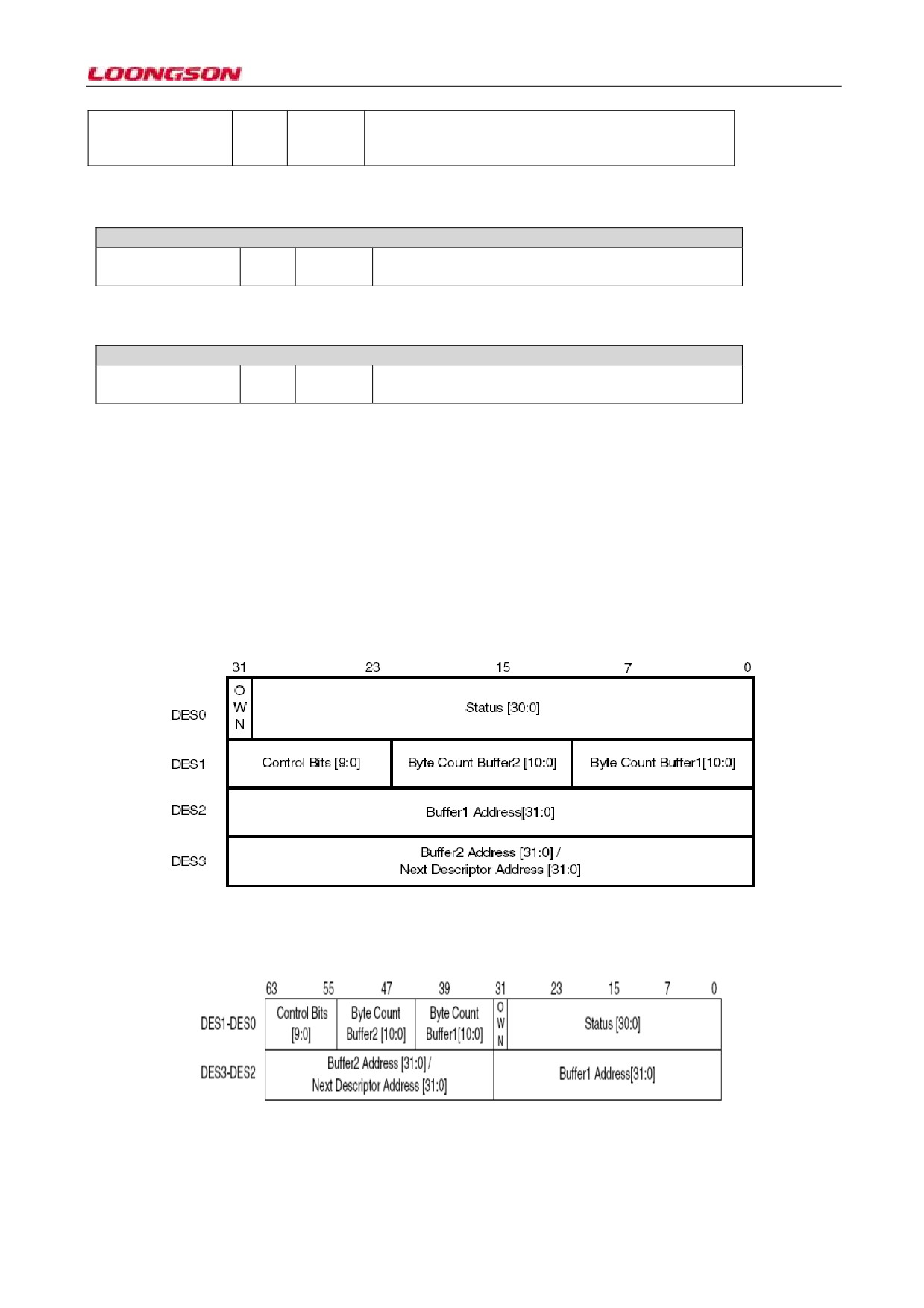
Each DMA descriptor includes two data buffers, two byte count buffer, and two pointer of data buffer address.
Note: the descriptor address must guarantee that the connected system bus bit width is aligned and the system byte
order is the same (little end by default)
Figure 11-1 Basic format of DMA descriptor (little end 32bit bus)
Figure 11-2 Basic format of DMA descriptor (little end 32bit bus)
-78-
11.3.2 DMA receive descriptor
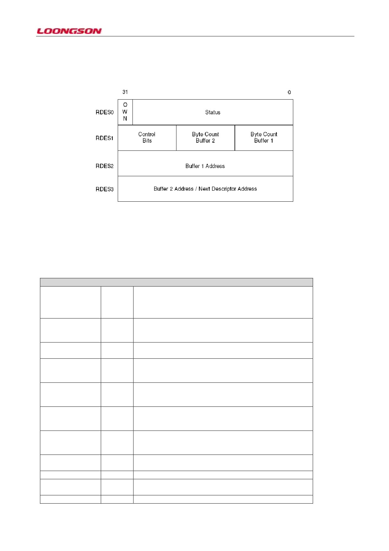
CMAC subsystem needs at least two receive descriptors in operating mode to normally receive one network data
packet. When processing one network data packet, its internal receive module always tries to obtain the next
receive descriptor. Each network data packet is called one frame.
Figure 11-3 Basic format of DMA receive descriptor (small end 32bit bus)
11.3.2.1 RDES0
RDES0 includes the current receive frame status, length and all circumstances of the descriptor (owned by host or
DMA). Details of RDES0 see table below.
RDES0 bit
OWN
31
When the bit is 1, it indicates the descriptor belongs to DMA
All modes
control, and when the bit is 0, it indicates the descriptor belongs
to DMA control. When DMA module finishes one transmission,
the bit will be cleared automatically.
AFM: Destination
30
When the bit is 1, it indicates that the current data frame target
Address Filter 1
address doesn’t comply with the internal frame target address
filter of GMAC.
FR: Frame length
29:16
It indicates receiving the length of the current frame. When ES
Frame length
bit is 0, it’s significant.
ES: Error Summary
15
It indicates whether the current frame is wrong, and its value is
RDES[0], RDES[1], RDES[3], RDES[4], RDES[6], RDES[7],
RDES[11] and RDES[14] bits or (OR) operation.
DE: Descriptor Error
14
When the bit is 1, it indicates that the buffer pointed by current
descriptor doesn’t comply with the frame or OWN is 0 (host
control)
SAF: Source Address
13
When the bit is 1, it indicates that the current data frame target
Filter Fail
address doesn’t comply with the internal frame source address
filter of GMAC.
LE: Length Error
12
When the bit is 1, it indicates that the length of the current
receive frame doesn’t comply with the default length. When the
Frame Type bit is 1, and CRC Error bit is 0, it’s significant.
OE: Over Flow Error
11
When the bit is 1, it indicates that when the frame is received,
GMAC internal RxFIFO overflow.
VLAN: VLAN Tag
10
When the bit is 1, it indicates the frame type is VLAN.
FS: First Desciptor
9
When the bit is 1, it indicates the buffer pointed by current
descriptor is the first saved buffer of the current receive frame.
LS: Last Descriptor
8
When the bit is 1, it indicates the buffer pointed by current
-79-
descriptor is the last saved buffer of the current receive frame.
IPC
Checksum 7
When the bit is 1, if IPC check function is enabled, it indicates
Error/Giant Frame
that the IPv4 head check value of the current frame doesn’t
comply with the value of frame internal check domain. If it’s
disabled, it indicates that the current frame is a giant frame
(more than 1518 bytes long)
LC: Late collision
6
When the bit is 1, it indicates that in half-duplex mode, when
the current frame receives, one late collision occurs.
FT: Frame Type
5
When the bit is 1, it indicates the current frame is an Ethernet
frame. When the bit is 0, it indicates the current frame is a
IEEE802.3 frame.
RIWT:
Receive
4
When the bit is 1, it indicates the current clock value exceeds
Watchdog Timeout
the value of Watchdog circuit clock in receive module, namely,
the receive frame timeout
RE: Receive Error
3
When the bit is 1, it indicates the internal module goes wrong
when receiving the current frame. Internal signal
Rxer is set to 1 and rxdv is set to 1
DE: Dribble bit Error
2
When the bit is 2, it indicates the length of the receive frame
isn’t an integer, namely, the total length is an odd bit. It’s
significant only in mii mode.
CE: CRC Error
1
When the bit is 1, it indicates the internal CRC goes wrong
when receiving the current frame. Only in last
descriptor(RDES0[8], this bit is significant.
RX
MAC:0
When the bit is 1, it indicates when receiving the current frame,
Checksum/payload
the internal RX MAC register block 1-15 has one address
Checksum Error
matching the current frame. When the bit is 0, it indicates the
RX MAC register block 0 matches the receive frame destination
address. When Full Checksum Offload Engine is enabled, if the
bit is
1, it indicates the frame TCP/UDP/ICMP check error.
When the bit is 1, it also indicates the current frame actual
receive length doesn’t comply with the internal record length.
11.3.2.2RDES1
RDES1 has recorded the buffer size pointed by descriptor, and the organization form of the descriptor (ring or
chain).
RDES1 bit
Disable
Intr
in
31
When the bit is 1, it indicates after the frame receive completes,
Completion
the RI bit (CSR5[6]) in STATUS register won’t be set. In this
way, the host can’t detect such interrupt.
Reserved
30:26
RER: Receive End of 25
When the bit is 1, it indicates the descriptor is the last in the
Ring
ring descriptor link table, and the address of the next descriptor
is the base address of the receive descriptor.
RCH:
Second24
When the bit is 1, it indicates that the second buffer address in
Address Chained The
descriptor points the address of the next descriptor. When the
second buffer also
bit is
0, it indicates the address points to the second buffer
points to the next
address. When the bit is
1, the value of RDES1[21-11] is
chain descriptor
insignificant, and RDES1[25] has a higher priority than
RDES1[24](represent ring instead of chain)
Reserved
23:22
RBS2:
Receive21:11
This domain indicates the size of data buffer2. Based on the
Buffer Size 2
width 32/64/128 of the system bus, the size of buffer2 should be
integral multiples of 4/8/16. Unknown results will be caused if
there is no satisfaction. When the domain in RDES1[24] is 0,
it’s significant.
-80-
RBS2:
Receive10:0
This domain indicates the size of data buffer1. Based on the
Buffer Size 1
width 32/64/128 of the system bus, the size of buffer1 should be
integral multiples of 4/8/16. Unknown results will be caused if
there is no satisfaction. This domain has always been valid. If
the threshold is 0, DMA will automatically access buffer 1 or
the next receive descriptor.
11.3.2.3RDES2
This domain has recorded the address of data receive buffer 1.
RDES2 bit
Buffer1
Address
31:0
The field has recorded the 32bit physical address of data receive
Pointer
buffer1. The physical address has no default alignment
requirements. When CMAC DMA aligns the bus data 32/64/128
bit, the low 2/3/4 bit of the address is ignored.
11.3.2.4 RDES3
This domain has recorded the address of data receive buffer 2.
RDES3 bit
31:0
The field has recorded the 32-bit physical address of data receive
Buffer2
Address
buffer2. The physical address has no default alignment
Pointer
requirements. When CMAC DMA aligns the bus data 32/64/128
bit. If the descriptor in connected by chain, the field records the
address of the next descriptor.
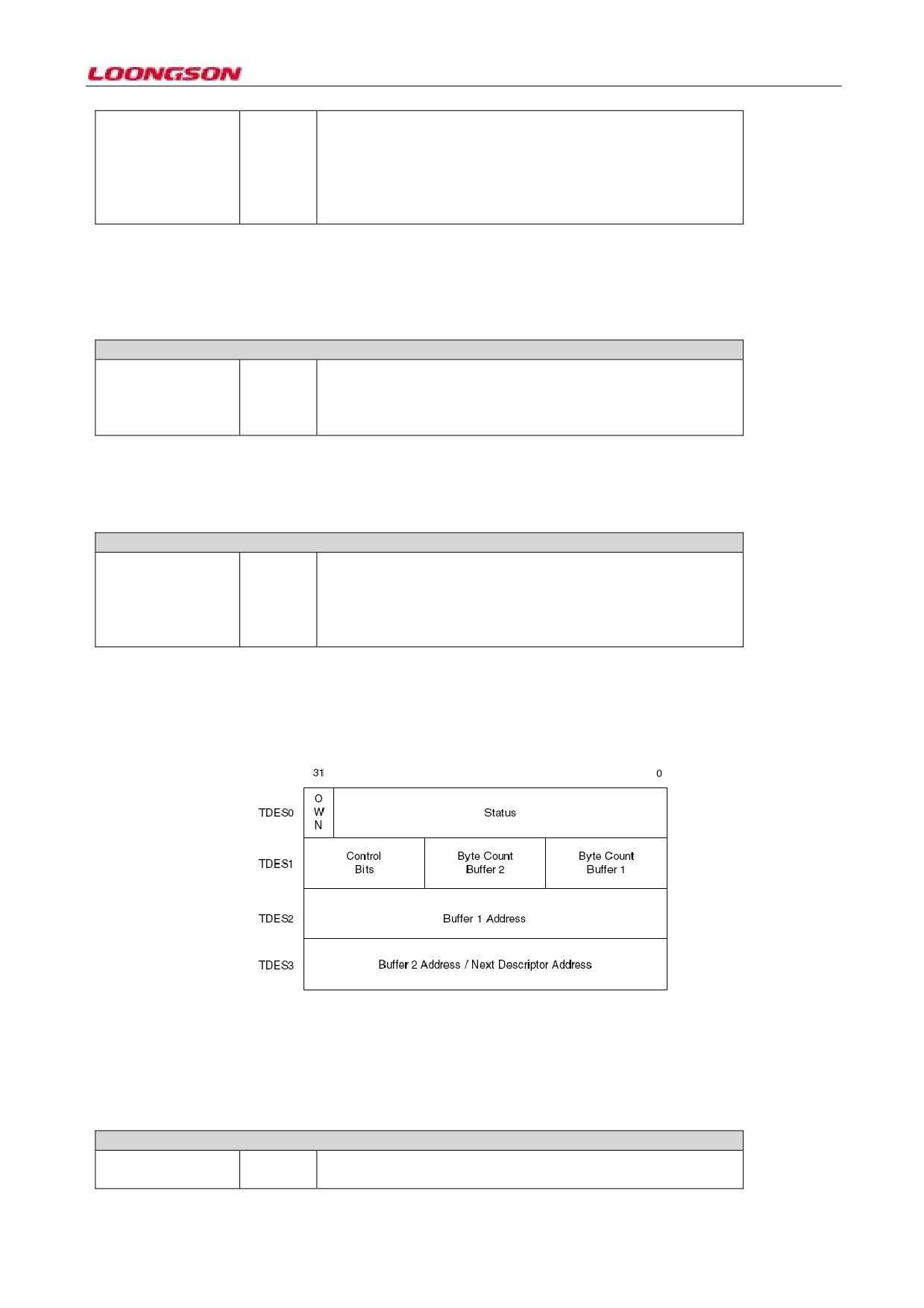
11.3.3 DMA transmit descriptor
The formats of transit descriptor and receive descriptor are basically same. Each descriptor address need to be
aligned based on bus width (32/64/126bits).
Figure 11-4 Basic format of DMA transmit descriptor (little tailing end 32-bit bus)
11.3.3.1TDES0
TDES0 includes the state of transmit frame and messages of transmit descriptor.
TDES0 bit
OWN
31
When the bit is 1, it indicates the descriptor belongs to DMA
control, and when the bit is 0, it indicates the descriptor belongs
-81-

to DMA control. When DMA module finishes one transmission,
the bit will be cleared automatically.
Reserved
30:18
TTSS: Tx Time
When IEEE1588 function is enabled, if the bit is 1, it indicates
Stamp Status
the time stamp message of this transmit frame has been saved in
17
TDES2 and TDES3. Or the bit shall be reserved
IHE: IP Header
16
When the bit is 1, it indicates the internal check module finds
the wrong IP head of this transmit frame, and won’t change the
domain.
ES: Error Summary
15
It indicates whether the current frame is wrong, and its value is
RDES[0], RDES[1], RDES[3], RDES[4], RDES[6], RDES[7],
RDES[11] and RDES[14] bits or (OR) operation.
JT: Jabber Timeout
14
When the bit is
1, it indicates GMAC transmit module
encounters Jabber timeout.
FF Frame Flushed
13
When the bit is 1, it indicates the software sends a refresh
command, and cause DMA/MTL to refresh all internal frames.
PCE: Payload
12
When the bit is 1, it indicates the internal loading check mode
insert the check number in the transmit frame
Checksum Error
It is an error. This bit is significant when the load check module
is enabled
LC: Loss of Carrier
11
When the bit is 1, it indicates the carried signal is lost during
frame transmission (gmii_crs signal several cycles aren’t set)
NC: No Carrier
10
When the bit is 1, it indicates that the carried signal of PHY has
been set during transmission.
LC: Late Collision
9
When the bit is 1, it indicates that in half-duplex mode, when
the current frame receives, one late collision occurs.
EC:
Excessive8
When the frame is 1, it indicates 16 collisions occur before the
Collision
current frame is sent.
VF: VLAN Frame
7
When the bit is 1, it indicates that the current transmit frame is a
VLAN frames
VLAN frame.
CC Collsion Count
6:3
This domain indicates the total collision number before the
successful transmission of the current frame
ED:
Excessive2
When this bit is 1, it indicates current frame transmission is
Deferral
completed.
UF: Underflow Error
1
When the bit is 1, it indicates that overflow error occurs in
current frame transmission, namely, data transmission.
buffer is too small or unavailable
DB: Defered Bit
0
When the bit is 1, it indicates that the transmission is delayed,
Frame Flushed
and it’s only significant in half-duplex mode.
11.3.3.2TDES1
TSESI includes the buffer size and other control and status bits of some descriptor ring/chain connection.
TDES1 bit
IC: Interruption on
31
When the bit is 1, it indicates that after the frame transmit
Complete
finishes, the TI bit in STATUS register will be set (CSR5[0])
LS: Last Segment
30
When the bit is 1, it indicates the current buffer includes the last
segment of one frame data (if the frame is divided into several
segments)
FS: First Segment
29
When the bit is 1, it indicates the current buffer includes the
first segment of one frame data (if the frame is divided into
several segments)
CIC:
Checksum 28:27
This domain controls whether the control internal module fills
Insertion Control
out check data in transmit frame.
Value: 2'b00: No insertion checksum
-82-
2'b01: Insertion IPV4 header checksum
2'b10: When the pseudo-header exists, TCP/UDP/ICMP full
check data are filled out.
2'b11: TCP/UDP/ICMP full check data are always filled out.
DC Disable CRC
26
When the bit is 1, CMAC hardware doesn’t add CRC check
data at the end of each transmit frame.
TER: Transmit End
25
When the bit is 1, it indicates the descriptor is the last in the
of Ring Descriptor
ring descriptor link table, and the address of the next descriptor
is the base address of the transmission descriptor.
TCH:
Second24
When the bit is 1, it indicates that the second buffer address in
Address Chained
descriptor points the address of the next descriptor. When the
The second buffer
bit is
0, it indicates the address points to the second buffer
address pointer
address. When the bit is
1, the value of RDES1[21-11] is
insignificant, and RDES1[25] has a higher priority than
RDES1[24](represent ring instead of chain)
DP: Disable Padding
When the bit is 1, it indicates the GMAC won’t fill out the
23
empty data in data packet with the length smaller than 64 bytes
TTSE: Transmit Time
22
When the bit is 1, the internal module will be started to compute
Stamp Enable
IEEE1588 hardware time stamp, and when TDES1[29] is 1, it’s
significant.
TBS2:
Transmit
21:11
This domain indicates the size of data buffer2. When
Buffer Size 2
TDES1[24] is 1, this domain is insignificant.
TBS1:
Transmit10:0
This domain indicates the size of data buffer1. This domain has
Buffer Size 1
always been valid. If the threshold is 0, DMA will automatically
access buffer 1 or the next receive descriptor.
11.3.3.3TDES2
This domain has recorded the address of data transmission buffer 1.
TDES2 bit
Buffer1
Address31:0
The field has recorded the 32bit physical address of data receive
Pointer
buffer1. The physical address has no default alignment
Transmit
buffer1
requirements. When CMAC DMA aligns the bus data 32/64/128
address
bit, the low 2/3/4 bit of the address is ignored.
11.3.3.4TDES3
This domain has recorded the address of data transmission buffer 2.
TDES3 bit
Buffer2
Address31:0
The field has recorded the 32-bit physical address of data receive
Pointer
buffer2. The physical address has no default alignment
Transmit
buffer2
requirements. When CMAC DMA aligns the bus data 32/64/128
address
bit, the low 2/3/4-bit of the address is ignored. If the descriptor is
connected by chain, this domain records the address of the next
descriptor.
11.4 Software Programming Guide
DMA initialization:
1 Software reset (reset) MAC
2. Wait for reset completion (search DMA reg0[0])
3. Program the following domain of DMA reg0
a. MIX-BURST and AAL(DMA reg0[26], [25])
b. Fixed-burst or undefined-burst(DMA reg0[16])
c. Burst-length and Burst-mode
-83-
d. Descriptor Length (Only in ring, is it effective)
e. Tx and Rx arbitration scheduling
4. Program AXI Bus Mode Reg
a. If the Fixed-burst is selected, it’s necessary to set the maximum burst length in the register.
5. It has created the transmit and receive descriptor chains respectively, and chosen ring mode or chain mode for
connection, and their OWN bits of receive descriptor is set to 1 (owned by DMA)
6. Before the software enables DMA descriptor, it must guarantee three are at least three descriptors in
transmit/send descriptor.
7. Write the starting address of the receive and transmit descriptor chain tables to DMA reg 3, 4
8. Configure the following bit in DMA reg6(DMA mode operation)
a. Received/transmitted Store and Forward
b. Received/transmitted threshold control
c. Hardware flow control enable
d. Error frame and unidentified correct frame skipping (forwarding enable)
e. OSF mode
9. Write 1 to DMA reg6(Status reg), and clear all interrupt requests
10. Write 1 to DMA reg7(interrupt enable reg), and enable all interrupts
11. Write 1 to DMA reg6[1], [13], enable transmit and receive DMA
MAC initialization:
1 Correctly configure the supporting PHY chips
2. Correctly configure MAC reg4(GMII Address Register), make it normally access PHY related register
3. Read MAC reg5(GMII Data Register) to obtain messages such as link, speed and mode (duplex) of the current
PHY
4 Configure MAC address
5. If the harsh filtering is enabled, it’s necessary to configure the hash filtering
6. Configure the following domain of MAC reg1(Mac Frame filter), conduct the frame filtering
a. Receive all
b. Promiscuous mode
c. Hash or perfect filter
d. Groupcast and multicast filter settings, etc.
7. Configure the following domain of MAC reg6(Flow control register)
a. Pause time and other pause control bit
b. Receive and transmit flow control bit
C. Busy flow control / follow-up pressure enable
8. Configure the interrupt mask register (Mac reg15)
9. Rightly configure MAC reg0 based on previously obtained line message (link, speed, mode)
10. Configure MAC reg0[2], [3] to enable transmit and enable modules in MAC
General processes of transmit and receive:
1. After detecting transmit or receive interrupt, search the corresponding descriptor to judge whether it belongs to
host, and read the data in descriptor
2. After finishing reading the data in descriptor, clear all descriptor bits and set their OWN bits, and make it
continue transmitting/receiving data
3. If the current transmit or receive descriptors don’t belong to DMA(OWN=0), the DMA module will enter into
the suspended state. When the data need transmitting/receiving, write 1 to DMA Tx/Rx POLL register, and enable
DMA module again Note: the receive descriptor should always belong to DMA(OWN=1) when idle.
4. Transmit and receive descriptors comply with the real-time information of corresponding buffer address, and
can be obtained by searching DMA reg18, 19, 20, 21.
11.5 IEEE 1588 Support
MAC controller supports IEEE 1588 clock synchronous protocol. IEEE 1588 defines that the protocol with
technologies such as LAN, distributed object to implement accurate clock synchronous proofreading, measuring
and control systems. IEEE1588 protocol is widely applicable to support heterogeneous systems with different
-84-
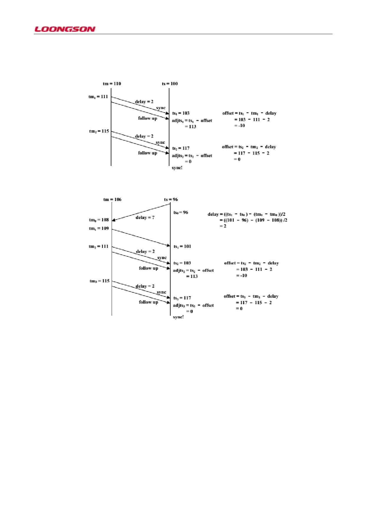
clock characteristics, and provide the full-system sub-second precision synchronization. The following two figures
provide two different clock system synchronization based on IEEE1588 protocol. Figure 1 is the process where
the host cycle sends the synchronous message to all slave devices in internet, and Figure 2 is the process that the
slave synchronizes the host synchronously.
Figure 11-5 Period clock synchronization process
Figure 11-6 Slave proactive synchronization process
During the synchronization of master and slave devices, the sent message frame is called ptp (precious time
protocol). See IEEE1588 protocol for the specific synchronization process. The entire clock synchronization
proofreading process is basically finished in internet UDP protocol layer, and MAC controller hardware only
needs to support the transmit and receive time functions of ptp packets, namely, the tm/s in above figure.
IEEE1588 software programming guide:
To enable IEEE1588 time stamp function, set Register 448 Time Stamp Control Register bit0 to 1. But in order to
use the function normally, the following relevant initialization work must be completed in MAC initialization
phase:
IEEE1588 initialization:
1. Set the bit9 of register 15 to 1, and switch off the system interrupt triggered by time stamp.
2. Set the bit0 of time stamp control register (reg 448) to 1, and enable time stamp function.
3. Set Register 449 Sub-Second Increment Register based on ptp clock frequency.
4. If you use Fine Correction approach, set register (Register 454 Time Stamp Addend register) and set the bit 5 of
-85-
time stamp control register (reg 448) to 1 (addend reg update)
5. The bit5 of rolling time stamp control register is set to 0.
6. Enable the Fine Update method by setting the bit1 of time stamp control register to 1 (if necessary).
7. Set the Time Stamp High Update and Time Stamp Low Update to corresponding values.
8. Set the bit2 of time stamp control register to 1 (time stamp initialization)
9. When writing the initial value to time stamp update register (registers 452 and 453 Time Stamp Update register),
the time stamp counter starts to work.
10. Enable transmit and receive modules of MAC to correctly operate time stamp function.
Note: when IEEE1588 function is disabled, follow and execute the above process to restart it.
System clock correction:
To synchronize or update the system clock in a process (coarse correction method), the following procedures are
adopted:
1. Write the offset (positive or negative) to time stamp update register (registers 452 and 453 Time Stamp Update
registers)
2. Set the bit3 of time stamp control register (reg 448) to 1.
3. When the bit of TSUPDT (reg448bit3) becomes 0, system clock adds or subtracts the offset in time stamp
update register in procedure 1.
-86-
12 USB Controller
12.1 Overview
Characteristics of USB host port 1C is as follows:
Ɣ It’s compatible with USB Rev 1.1 and USB Rev 2.0 protocols
Ɣ It’s compatible with OHCI Rev 1.0 and EHCI Rev 1.0 protocols
ƔSupport the USB device at LS (Low Speed) , FS (Full Speed) and HS (HighSpeed)
Ɣ Support one port, and suspend LS, FS or HS device.
USB host controller module includes a EHCI controller supporting HS device, and one OHCI controller supports
FS and LS devices. Therein, the EHCI controller is in master control status, and only when FS or LS devices are
suspended, can the control right be transferred to OHCI controller; only when FS or LS device is pulled up, will
control right return to EHCI controller.
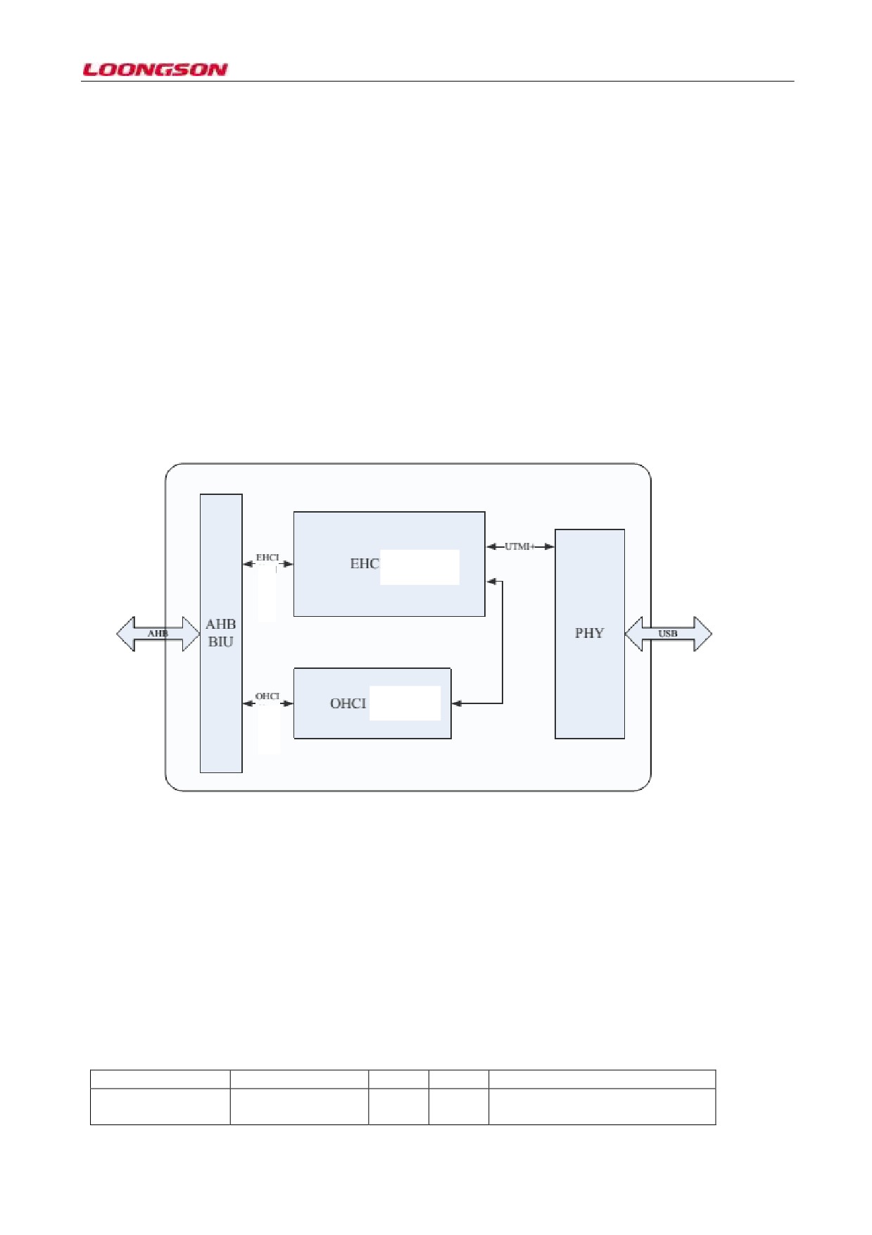
Meanwhile, the USB controller has integrated the AHB bus interface (compatible with AMBA Specification
Revision 2.0) for the communication with memory/application. The interconnection architecture chart of USB
controller and the outside is as shown in Figure 12-1:
Controller
Interface
Controller
Interface
Figure 12-1 USB host controller module
12.2 USB Host Controller Register
12.2.1 EHCI relevant registers
EHCI relevant registers include Capacity register, Operational register and EHCI implementation relevant register.
The USB host controller of 1C is compatible with EHCI Rev 1.0 protocol. For Capacity register and Operational
register, please refer to Enhanced Host Controller Interface Rev 1.0 Specification.
The base address of EHCI is equal to the base address of the below register plus offset.
12.2.2 Capability register
Name
Offset address
Width
Access
Note
HCCAPBASE
0x00
32
RO
The value is
32'h01000010 by
default.
-87-
HCSPARAMS
0x04
32
RO
The value is
32'h00001116 by
default.
HCCPARAMS
0x08
32
RO
The value is
32'h0000A010 by
default.
(Notes: USBBase is fixed as the starting address 0xbfe2_0000 of EHCI slave)
12.2.3 Operational Register
Name
Address
Width
Access
Note
USBCMD
0x10
32
R/W
USB host
controller
RO
command register
USBSTS
0x14
32
R/W
USB host controller status
RO
register
USBINTR
0x18
32
R/W
Interrupt set register of USB
host controller
FRINDEX
0x1C
32
R/W
USB host controller frame
index register
CTRLDSSEGMENT
0x02
32
R/W
Store the address of EHCI
control data structure
PERIODICLISTBASE
0x24
32
R/W
Store the initial address of
period data frame table
ASYNCLISTADDR
0x28
32
R/W
Store the initial address of
the next asynchronous queue
to execute
CONFIGFLAG
0x05
32
R/W
Configuration mode register
PORTSC 1
0x54
32
R/W
Port
1 status and control
register
PORTSC 2
0x58
32
R/W
Port
2 status and control
register
PORTSC 3
0x5c
32
R/W
Port
3 status and control
register
PORTSC 4
0x60
32
R/W
Port
4 status and control
register
PORTSC 5
0x64
32
R/W
Port
5 status and control
register
PORTSC 6
0x88
32
R/W
Port
6 status and control
register
(Notes: USBOPBase is fixed as the starting address of EHCI slave + `h10)
12.2.4 EHCI implementation relevant register
EHCI implementation relevant register is described as follows.
Name
Address
Width
Access
Note
INSNREG00
0x90
32
R/W
Frame length configuration register
INSNREG01
0x94
32
R/W
Data packet buffer OUT/IN
threshold register
INSNREG02
0x98
32
RO
Data packet buffer depth register
INSNREG03
0x9c
32
R/W
Reference to the detailed register
description
INSNREG04
0xa0
32
R/W
For Debug
INSNREG05
0xa4
32
R/W
UTMI configuration (default setting) ,
control and status registers
INSNREG06
0xa8
32
RO
AHB error status register
INSNREG07
0xa:
32
RO
AHB Master error address register
-88-
INSNREG08
0xb0
32
RO
HSIC enable register
INSNREG00 register (disable)
INSNREG01 register
Bit field
Access
Reset value
Note
31:16
R/W
16'h0020
OUT threshold (the unit is 4 bytes). Once the data fetched from
system memory reaches the OUT threshold, the USB
transmission starts, at least 16bytes.
15:0
R/W
16'h0020
IN threshold (the unit is 4 bytes). Once the data fetched from
Packet Buffer reaches the IN threshold, the USB transmission
starts, at least 16bytes.
INSNREG02 register
Bit field
Access
Reset value
Note
31:12
Reserved
20'h0
Reserved
11:0
RO
12'h0020
Data packet buffer depth (the unit is 4 bytes)
INSNREG03 register
Bit field
Access
Reset value
Note
31:13
Reserved
19'h0
Reserved
12:10
RO
3'h0
When the field defines the extra delay of phy_clks, the delay is
added to “Tx-Tx turnaround Delay”.
9
RO
1'h0
Set 1: to force the host controller to obtain the cycle data frame
table for each micro-frame in a frame
Set 0: the host controller obtains the cycle data frame table from
each micro-frame 0 in a frame
8:1
R/W
8'h0
The time can tolerate the offset, and the field is used to indicate
the byte number to add for tolerating and computing the available
time. To computer the available time is added for the future
transmission elasticity, and the user program default doesn’t need
to change this field.
0
RO
1'h0
Break Memory Transaction mode
Set to 1: enable this function
Set to 0: disable this function
INSNRE04 register (it’s only used for debugging, and the software doesn’t need to change this register)
Bit field
Access
Reset value
Note
31:6
Reserved
26'h0
Reserved
5
R/W
1'h0
Set 1: disable automatic function. Namely, when the software
clears Run/Stop bit, USB host controller wake up the
Suspend port
Set 0: enable automatic function. When the software rests
Run/Stop bit, Suspend signal will be set to 1.
4
R/W
1'h0
Set 1: disable NAK reload repair
Set 0: enable NAK reload repair
3
Reserved
1'h0
Reserved
2
R/W
1'h0
Set 1: shorten port enumeration time (simulation)
1
R/W
1'h0
Set to 1: 17, 15:4 and 2:0 bits in HCCPARAMS register can be
written
0
R/W
1'h0
Set to 1: HCSPARAMS writable register
-89-
INSNREG05 register
Bit field
Access
Reset value
Note
31:18
Reserved
14'h0
Reserved
17
RO
1'h0
Set 1: it indicates a write operation is conducted for the
register, and the hardware is executing.
Set to
0: it indicates the hardware has completed the
operations
16:13
R/W
5'h0
Port number
12
R/W
4'h1
VControlLoadM
Set to 1: NOP
Set to 0: Load
11:8
R/W
4'h0
VControl
7:0
RO
4'h0
VStatus
INSNREG06 register
Bit field
Access
Reset value
Note
31
R/W
1'h0
Once AHB make mistakes and is captured, set it 1, write 0 and
clear this field.
30:12
Reserved
19'h0
Reserved
11:9
RO
3'h0
In the event of AHB error, the value of HBURST in control field
8:4
RO
5'h0
The burst expected beats of AHB error
3:0
RO
4'h0
In the current burst, the completed beats before AHB error
INSNREG07 register
Bit field
Access
Reset value
Note
31:0
RO
32'h0
AHB control segment address in error
INSNREG08 register
Bit field
Access
Reset value
Note
31:0
RO
1'b0
HSIC enable
12.3 OHCI Relevant Register
OHCI relevant registers include Operational register and OHCI implementation relevant register. The USB host
controller of 1C is compatible with OHCI Rev 1.0 protocol. For Operational register details, please refer to Open
Host Controller Interface Rev 1.0 Specification.
The base address of OHCI is 0xbfe280000 and the address of the below register is equal to the base address plus offset.
12.3.1 Operational Register
Name
Address
Width
Access
Note
HcRevision
0x00
32
-
Control and status
HcControl
0x04
32
-
HcCommonStatus
0x08
32
-
HcInterruptStatus
0x0C
32
-
HcInterruptEnable
0x10
32
-
HcInterruptDisable
0x14
32
--
-90-
HcHCCA
0x18
32
-
Memory pointer
HcPeriodCuttentED
0x1C
32
-
HcControlHeadED
0x20
32
-
HcControlCurrentED
0x24
32
-
HcBulkHeadED
0x28
32
-
HcBulkCurrentED
0x2C
32
-
HcDoneHead
0x30
32
-
HcRmInterval
0x34
32
-
Frame counter
HcFmRemaining
0x38
32
-
HcFmNumber
0x3C
32
-
HcPeriodicStart
0x40
32
-
HcLSThreshold
0x44
32
-
HcRhDescriptorA
0x48
32
-
Concentrator
HcRhDescriptorB
0x0C
32
-
HcRhStatus
0x50
32
-
HcRhPortStatus1
0x54
32
-
HcRhPortStatus2
0x58
32
-
12.3.2 OHCI implementation relevant register
Except the standard OHCI operation register, it has also implemented two additional registers (register offset 0x98
and 0x9C) to report the error state of AHB.
Name
Address
Width
Access
Note
INSNREG06
0x98
32
RO
AHB error status register
INSNREG07
0x9c
32
RO
AHB Master error address register
INSNREG06 register
Bit field
Access
Reset value
Note
31
R/W
1'h0
Once AHB make mistakes and is captured, set it to 1, write 0 and
clear this field.
30:12
RO
19'h0
Reserved
11:9
RO
3'h0
In the event of AHB error, the value of HBURST in control field
8:4
RO
5'h0
The burst expected beats of AHB error
3:0
RO
4'h0
In the current burst, the completed beats before AHB error
INSNREG07 register
Bit field
Access
Reset value
Note
31:0
RO
32'h0
AHB control segment address in error
-91-
13 OTG Controller
13.1 Overview
1C OTG supporting characteristics are as follows:
Ɣ Support HNP and SRP protocols;
Ɣ Embedded DMA without occupying processor band width for the mobile data between OTG and external storage
Ɣ In device mode, HS device (480Mbps);
ƔIn host mode, it only support HS device (480Mbps);
Ɣ In device mode, it supports two directional endpoints, with only the defaulted endpoint0 support control
transmission;
Ɣ In device mode, it supports the transmission in 2 IN directions at most at the same time;
Ɣ In host mode, it supports 6 channels, and the software can set each channel direction.
Ɣ In host mode, it supports the periodic OUT transmission.
13.2 Register Description
The application reads and writes the control and status registers (CSRs) in OTG controller by AHB slave interface,
and these registers are 32bit wide, and the register address is 32bit aligned.
Note: in host mode and device mode, the accessible register block only includes Core Global register block, Power
and Clock Gating register block, Data FIFO Access register block and Host Port register block. When the OTG
controller is in host or device mode, the register in another mode can’t be accessed. In the event of illegal register
read and write, the mode mismatch interrupt will occur, and such interrupt will be reflected in Core Interrupt
Register.
When the OTG converts from one mode to another, the register in this mode must be reconfigured, because the
status of the register after conversion is the same with that in restart.
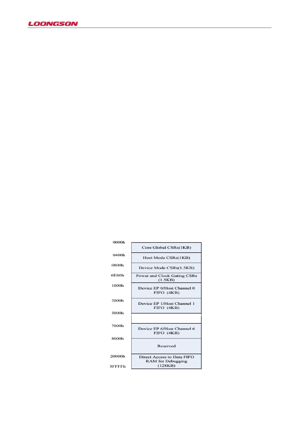
The address mapping of CSR is fixed. The registers in Host mode and Device mode are located in different
address spaces, and all registers all work in AHB clock field. The figure below displays the address mapping
relation of CSR.
Figure 13-1 OTG CSRs address mapping
The following chapter has listed OTG all registers and their offset address, and their base address is 0xbfe0_0000.
-92-
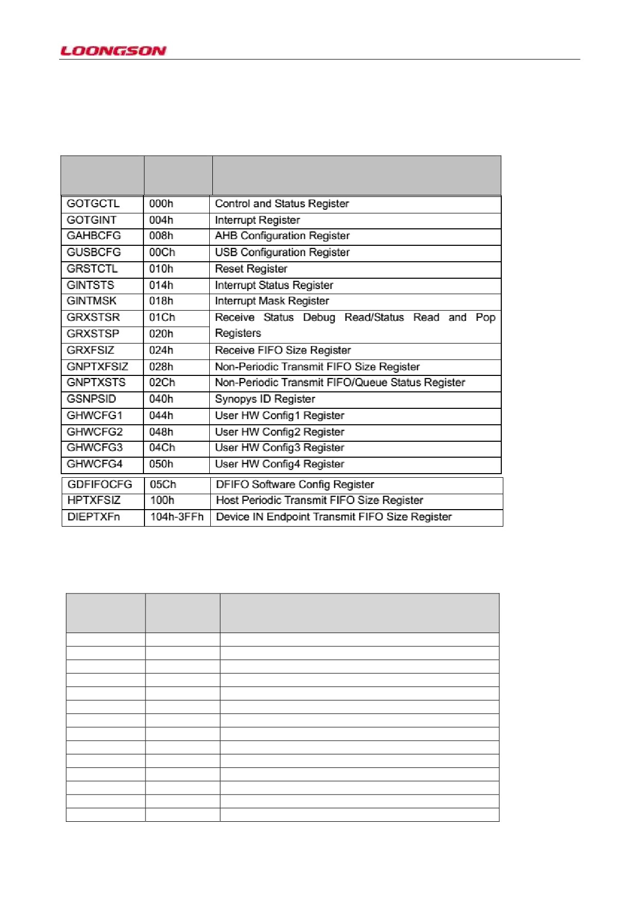
13.2.1 Global Control and Status Registers (Global CSR Map)
No matter whether OTG works in host mode or Device mode, this register block can be accessed, and their
corresponding offset addresses are shown in the table below:
Register
Offset
Register name
abbreviated
address
name
13.2.2 Host Mode Control and Status Register (Host Mode CSR)
Once OTG operates in Host mode, this register block will be reset.
Register
Offset address
Register name
abbreviated
name
HCFG
400h
Host Configuration
HFIR
404h
Host Frame Interval Register
HFNUM
408h
Host Frame Number/Frame Time Remaining Register
40ch
Reserved
HPTXSTS
410h
Host Periodic Transmit FIFO/Queue Status Register
HAINT
414h
Host All Channels Interrupt Register
HAINTMSK
418h
Host All Channels Interrupt Mask Register
HPRT
440h
Host Port Control and Status Register
444h-4FCh
Reserved
HCCHARn
500h
Moving the Host Core to Test Mode
HCSPLTn
504h
Host Channel-n Split Control Register (HCSPLTn
HCINTn
508h
Host Channel-n Interrupt Register (HCINTn)
HCINTMSKn
50Ch
Host Channel-n Interrupt Mask Register (HCINTMSKn
HCTSIZn
510h
Host Channel-n Transfer Size Register (HCTSIZn
-93-
HCDMAn
514h
Host Channel-n DMA Address Register
518h
Reserved
HCDMABn
51Ch
Host Channel-n DMA Buffer Address Register
HCCHARn
520h-53Ch
Host Channel-n Characteristics Register
540h-55h
…
6C0h—6DCh
6E0h-6FCh
6FDh-7FFh
13.2.3 Device Mode Control and Status Register (Device Mode CSR)
Once OTG operates in Device mode, this register block will be reset.
Register
abbreviatedOffset address
Register name
name
DCFG
800h
Device Configuration Register
DCTL
804h
Device Control Register
DSTS
808h
Device Status Register
41Ch
Reserved
DIEPMSK
808h
Device IN Endpoint Common Interrupt Mask
Register
DOEPMSK
808h
Device OUT Endpoint Common Interrupt Mask
Register
DAINT
808h
Device All Endpoints Interrupt Register
DAINTMSK
41Ch
Device All Endpoints Interrupt Mask Register
DVBUSDIS
808h
Device VBUS Discharge Time Register
DVBUSPULSE
41Ch
Device VBUS Pulsing Time Register
DTHRCTL
830h
Device Threshold Control Register
DIEPEPMSK
834h
Device IN Endpoint FIFO Empty Interrupt Mask
Register
DIEPCTL0
900h
Device Control IN Endpint0 Control Register
808h
Reserved
DIEPCTLn
920-AE0h
Device Endpoint-n Control Register
DIEPINTn
808h
Device Endoint-n Interrupt Register
41Ch
Reserved
DIEPTSIZ0/DOEPTSIZ0
808h
Device Endpoint0 Transfer Size Register
DIEPTSIZn/DOEPTSIZn
808h
Device Endpointn Transfer Size Register
DIEPDMAn
808h
Device Endpoint-n DMA Address Register
DTXFSTSn
808h
Device IN Endpoint Transmit FIFO Status Register
DIEPDMAB0
41Ch
Device Endpoint-n DMA Buffer Address Register
DOEPCTL0
B00h
Device Control OUT Endpint0 Control Register
B04h
Reserved
DOEPCTLn
B20-BE0h
Device Endpoint-n Control Register
DOEPINTn
B08h
Device Endoint-n Interrupt Register
B0Ch
Reserved
DOEPTSIZ0
B10h
Device Endpoint0 Transfer Size Register
DOEPTSIZn
B10h
Device Endpointn Transfer Size Register
DOEPDMAn
B14h-CF4h
Device Endpoint-n DMA Address Register
DOEPDMAB0
B1Ch-CFCh
Device Endpoint-n DMA Buffer Address Register
13.2.4 Data FIFO Access Register MAP (DFIFO Access Register MAP)
No matter whether OTG operates in Host mode or Device mode, this register block can be accessed. This register
block is used to read and write the FIFO of endpoint or channel in given direction. In host mode, the FIFO in
channel direction is IN, and only the FIFO in this channel can be read; similarly, in host mode, the FIFO in
-94-

channel direction is OUT, and only the FIFO in this channel can be written.
Register name
Offset address
Read-write characteristics
Device IN Endpoint
0/Host
1000h-1FFCh
WO/RO
OUT Channel 0: DFIFO Write
Access
Device OUT Enpoint 0/Host IN
Channel 0: DFIFO Read Access
Device IN Endpoint
0/Host
2000h-2FFCh
WO/RO
OUT Channel 0: DFIFO Write
Access
Device OUT Enpoint 0/Host IN
Channel 0: DFIFO Read Access
Device IN Endpoint
14/Host
OUT Channel 14: DFIFO Write
Access
F000h-FFFCh
WO/RO
Device OUT Enpoint
14/Host
IN Channel
14: DFIFO Read
Access
Device IN Endpoint
15/Host
10000h-10FFCh
WO/RO
OUT Channel 15: DFIFO Write
Access
Device OUT Enpoint
15/Host
IN Channel
15: DFIFO Read
Access
13.2.5 Power and Clock Gating CSR Map
No matter whether OTG operates in Host mode or Device mode, this register block can be accessed. This register
block is used as power control and gating clock
Register
Offset address
Description
abbreviated name
PCGCCTL
E00h
Power and Clock Gating Control Register
13.3 Register Description
13.3.1 Register access characteristics
During the below description of register, one column of access characteristics are used to mark the read and write
characteristics of these registers. The following contents will list the specific meaning of these access
characteristics.
Read Only (RO)
Read only
Write Only(WO)
Write only
Read and Write(R_W)
Readable and writable
Read, Write, and SelfReadable and writable; the controller can self clear, and clearing
Clear(R_W_SC)
conditions have been explained in each field below in detail.
Read, Write, Self Set andReadable and writable; the controller can self set and clear, and setting
Self Clear
and clearing conditions have been explained in each domain below in
(R_W_SS_SC)
detail.
Read, Self Set, and Write
Readable; OTG controller can self set the bit; when the software writes
Clear
1 to the bit and complete clearing, no effect will be generated by
R_SS_WC
writing 0 to this bit. Conditions for setting OTG bit has been explained
in each domain below in detail.
Read, Write Set, and SelfReadable; OTG controller can write 1 to this bit and completes bit
-95-

Clear
setting; when the software self clears, the software can’t clear. Namely,
(R_WS_SC)
no effect will be generated by writing 1 to this bit. Conditions for OTG
clearing have been explained in each domain below in detail.
Read, Self Set, and SelfReadable; OTG controller can self set and clear; when the software
Clear or Write Clearwrites 1 to the bit and completes clearing, no effect will be generated
(R_SS_SC_WC)
by writing 0 to this bit. OTG specific bit setting and clearing conditions
are explained in each domain below in detail.
13.3.2 Global register
No matter OTG operates in host mode or Device mode, this register block can be accessed. When the OTG
converts from one operating mode to another, it’s unnecessary to instantiate these registers again.
Control and status register (GOTGCTL)
Offset address: 000h
OTG control and status register (GOTGCTL) controls OTG function and reflect its status.
file
Note
Operating mode
Reset value
Access
characterist
ics
31:21
Reserved file
Host; Device
RO
20
OTG version
Host;
1'b0
Rw
Ɣ1'b0: Version
1.3; this version OTGDevice
supports the SRP of Data line pulsing and
VBus pulsing.
Ɣ1'b1: Version
2.0; this version OTG
only supports the SRP of Data line pulsing.
19
B-session valid(BSesVld) specifies theDevice only
1'b1
RO
transceiver status in device mode.
Ɣ1'b0: B-session illegal
Ɣ1'b1: B-session legitimate
In OTG mode, this bit is used to decide
whether the device has been connected.
18
ssesion valid(ASesVld) specifies the statusHost only
1'b0
RO
of transceiver in host mode.
Ɣ1'b0: A-session illegal
Ɣ1'b1: A-session legitimate
In device mode, this bit is reserved.
17
Long/ShortDebounceTime
(DbncTime)Host only
1'b0
RO
specifies one debounce time finding the
connection
Ɣ1'b0: long debounce time is used as
physical connection (100ms + 2.5us)
Ɣ1'b1: short debounce time, used as soft
connection (2.5us)
16
Connector ID status
Host ;
1'b1
RO
In a connection event, it indicates the IDDevice
status
Ɣ1'b0: OTG working in the mode of
Device A
Ɣ1'b1: OTG working in the mode of
Device B
15:12
Reserved domain
Host; Device
RO
11
Device HNP enable bit (DevHNPEn)
Device Only
1'b0
R_W
Ɣ1'b0: HNP disable
Ɣ1'b1: HNP enable
10
Host Set HNP enable bit
Host only
1'b0
R_W
-96-

Ɣ1'b0: Host Set HNP isn’t enabled
Ɣ1'b1: Host Set HNP enable
9
HNP request
Device Only
1'b0
R_W
The software sets the bit and sends a HNP
request to host. When the bit of
GOTGINT.HstNegSucStsChng is set, this
software is cleared by writing 0 to the bit.
When the bit of HstNegSucStsChng is 0,
OTG controller clears the bit.
Ɣ1'b0: No HNP request
Ɣ1'b1: HNP request
8
HostNegotiationSuccess (HstNegScs)
Device only
1'b0
RO
When the host is exchanged
(Host
Negotiation), OTG controller asserts the
bit.
Ɣ1'b0: host negotiation failure
Ɣ1'b1: host negotiation success
7
B-Peripheral
Session
Valid
valueDevice only
1'b0
R_W
(BvalidOvVal)
When the bit of GOTGCTL.BvalidOvEn is
set, the bit of BValidOvVal is used reset
Bvalid signal.
¡ñ1'b0: When GOTGCTL.BvalidOvEn = 1,
the value of Bvalid signal is 0;
Ɣ1'b1: When GOTGCTL.BvalidOvEn=
1, the value of Bvalid signal is 1;
6
B-Peripheral Session Valid reset enableDevice only
1'b0
R_W
(BvalidOvEn)
This bit is used to make the software
override
Bvalid
signal
by
GOTGCTL.BValidOvVal bit.
Ɣ1’b1: the Bvalid signal value received
from PHY is reset by BvalidOvVal.
Ɣ1’b0: Bvalid signal reset function is
disabled, and the Bvalid signal used by
OTG controller is namely the value
received from PHY.
5
A-Peripheral Session Valid reset valueHost only
1'b0
R_W
(AvalidOvVal)
When the bit of GOTGCTL.AvalidOvEn is
set, the bit of AValidOvVal is used reset
Avalid signal.
Ɣ1’b0: When GOTGCTL.AvalidOvEn = 1,
the value of Avalid signal is 0;
Ɣ1'b1: When GOTGCTL.AvalidOvEn= 1,
the value of Avalid signal is 1;
4
A-Peripheral Session Valid reset enableHost only
1'b0
R_W
(AvalidOvEn) is used to make the software
override Avalid signal Bvalid signal by
GOTGCTL.AValidOvVal bit.
Ɣ1’b1: the Avalid signal value received
from PHY is reset by AvalidOvVal.
Ɣ1’b0: Avalid signal reset function is
disabled, and the Avalid signal used by
OTG controller is namely the value
received from PHY.
3
VBUS Valid reset value (VbvalidOvVal)
Host only
1'b0
R_W
-97-