Loongson 1C300 Processor User Manual (Version 1.0, 2014) - page 3
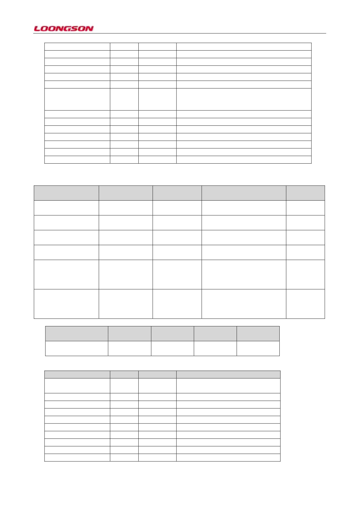
Reserved
28:24
0
RTC_int
23:21
0
RTC interrupt status bit
PWM_int
20:17
0
Corresponding 4-channel PWM interrupt status bit
Reversed
16
0
DMA_int
15:13
0
Corresponding 3-channel DMA interrupt status bit
Reversed
12:11
0
I2S_AC97_int
I2S or AC97 interrupt status bit. When ac97_en is
10
0
1, the bit is AC97 interrupt status bit, or it is I2S
interrupt status bit.
SPI1_int
9
0
SPI1 interrupt status bit
SPI0_int
8
0
SPI0 interrupt status bit
CAN1_int
7
0
CAN1 interrupt status bit
CAN0_int
6
0
CAN0 interrupt status bit
UART2_int
5
0
UART2 interrupt status bit
UART1_int
4
0
UART1 interrupt status bit
UART0_int
3:0
0
UART0 interrupt status bit
The second group of interrupt registers
Register name
Address
Read /
Function description
Reset value
Write (R / W)
INT1_SR
0xbfd0_1058
R
Interrupt status register 1
0x0
In common with INT0_SR
INT1_EN
0xbfd0_105c
R/W
Interrupt enable register 1
0x0
In common with INT0_EN
INT1_SET
0xbfd0_1060
R/W
Interrupt setting register 1
0x0
In common with INT0_SET
INT1_CLR
0xbfd0_1064
R/W
Interrupt clear register 1
0x0
In common with INT0_CLR
INT1_POL
0xbfd0_1068
R/W
Interrupt polarity selection
0x0
register 1
In common with interrupt
polarity selection register 0
INT1_EDGE
0xbfd0_106c
R/W
Interrupt edge selection register
0x0
1
Interrupt edge selection register
0
Register name
Address
Read / Write
Function
Reset value
(R / W)
description
INT1_SR
0xbfd0_1058
R
Interrupt status
register 1
INT1_SR
Bit
Default values
Description
Gpio[105:96]
31:22
0
GPIO[105:96] as interrupt input,
interrupt status bit
Reserved
21:20
0
I2C_int0
19
0
I2C0 interrupt status bit
I2C_int1
18
0
I2C1 interrupt status bit
I2C_int2
17
0
I2C2 interrupt status bit
Reserved
16
0
UART11_int
15
0
UART11 interrupt status bit
UART10_int
14
0
UART10 interrupt status bit
UART9_int
13
0
UART9 interrupt status bit
UART8_int
12:9
0
UART8 interrupt status bit
-38-
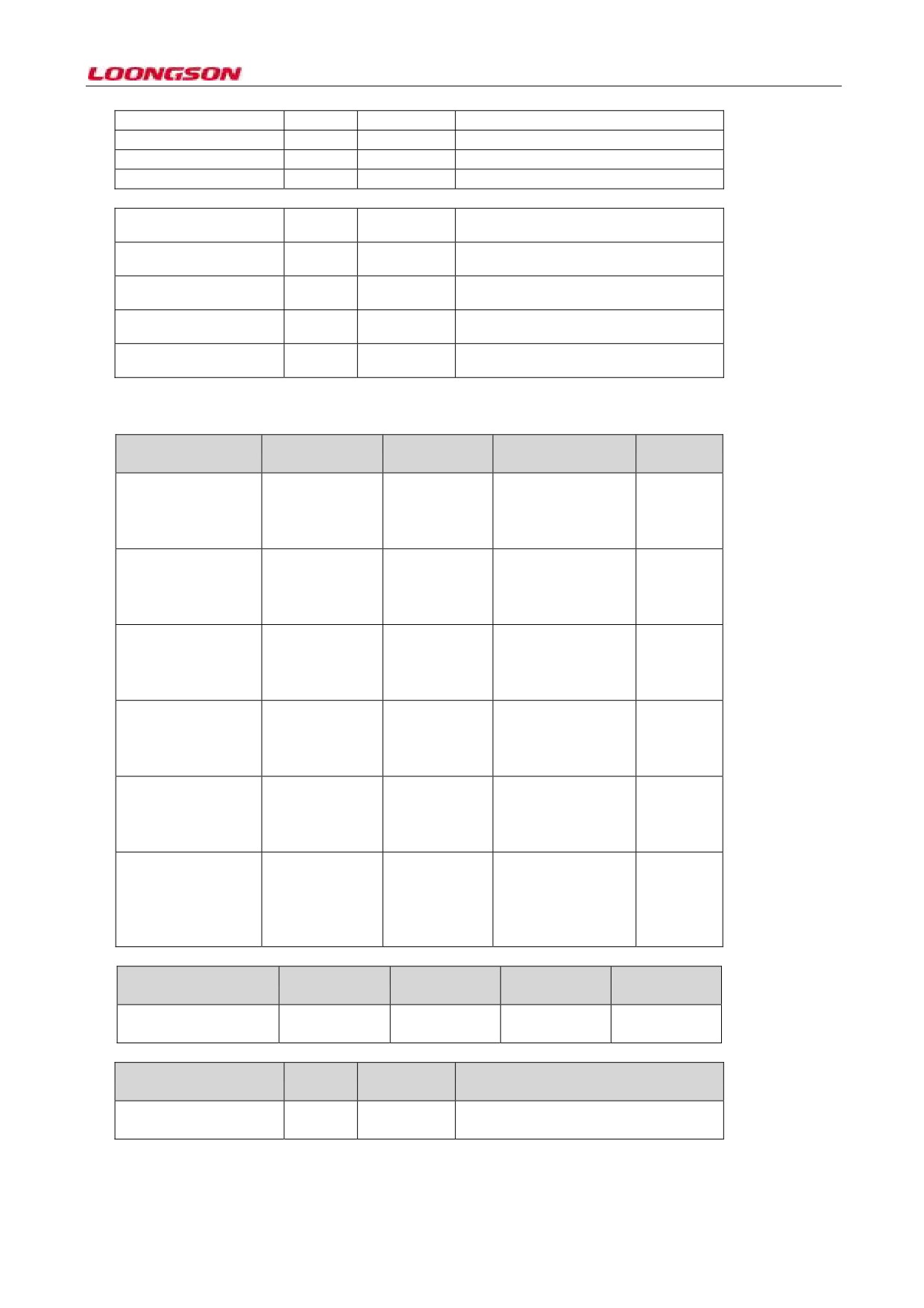
UART7_int
8
0
UART7 interrupt status bit
UART6_int
7
0
UART6 interrupt status bit
UART5_int
6
0
UART5 interrupt status bit
UART4_int
5
0
UART4 interrupt status bit
cam_int
4
0
CAMERA interrupt status bit
mac_int
3
0
MAC interrupt status bit
otg_int
2
0
OTG interrupt status bit
ohci_int
1
0
USB_OHCI interrupt status bit
ehci_int
0
0
USB_EHCI interrupt status bit
The third group of interrupt registers
Register name
Address
Read / Write
Function
Reset value
(R / W)
description
INT2_SR
0xbfd0_1070
R
Interrupt
status
0x0
register 2
In common with
INT0_SR
INT2_EN
0xbfd0_1074
R/W
Interrupt
enable
0x0
register 2
In common with
INT0_EN
INT2_SET
0xbfd0_1078
R/W
Interrupt
setting
0x0
register 2
In common with
INT0_SET
INT2_CLR
0xbfd0_107c
R/W
Interrupt
clear
0x0
register 2
In common with
INT0_CLR
INT2_POL
0xbfd0_1080
R/W
Interrupt
polarity
0x0
selection register 2
Interrupt
polarity
selection register 0
INT2_EDGE
0xbfd0_1084
R/W
Interrupt
edge
0x0
selection register 2
In common with
interrupt
edge
selection register 2
Register name
Address
Read / Write
Function
Reset value
(R / W)
description
INT2_SR
0xbfd0_1070
R
Interrupt status0x0
register 2
INT2_SR
Bit
Default
Description
values
GPIO[31:0]
31:0
0
GPIO[31:0] as interrupt input, interrupt
status bit
The fourth group of interrupt registers
-39-
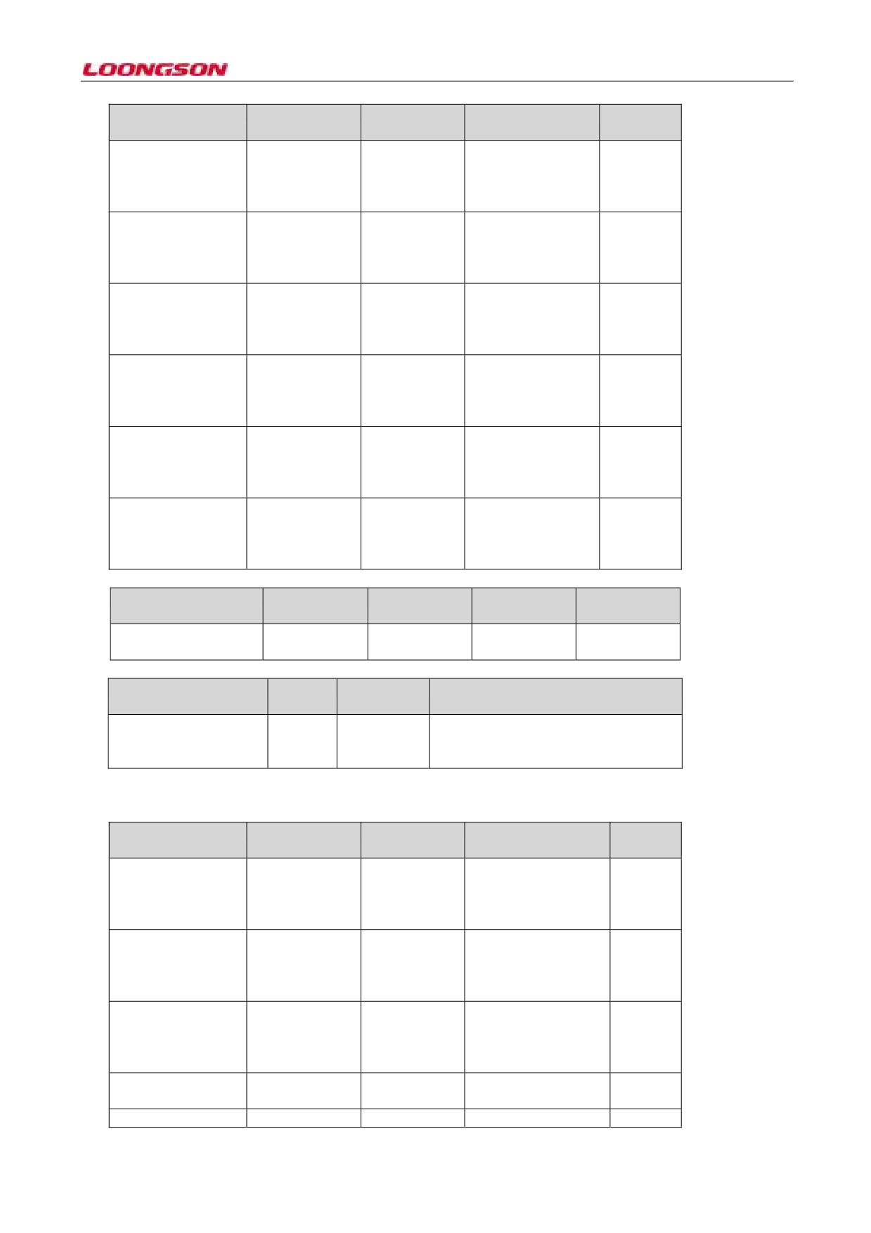
Register name
Address
Read / Write
Function
Reset value
(R / W)
description
INT3_SR
0xbfd0_1088
R
Interrupt
status
0x0
register 3
In common with
INT0_SR
INT3_EN
0xbfd0_108c
R/W
Interrupt
enable
0x0
register 3
In common with
INT0_EN
INT3_SET
0xbfd0_1090
R/W
Interrupt
setting
0x0
register 3
In common with
INT0_SET
INT3_CLR
0xbfd0_1094
R/W
Interrupt
clear
0x0
register 3
In common with
INT0_CLR
INT3_POL
0xbfd0_1098
R/W
Interrupt
polarity
0x0
selection register 3
In common with
INT0_POL
INT3_EDGE
0xbfd0_109c
R/W
Interrupt
edge
0x0
selection register 3
In common with
INT0_EDGE
Register name
Address
Read / Write
Function
Reset value
(R / W)
description
INT3_SR
0xbfd0_1088
R
Interrupt status0x0
register 3
INT3_SR
Bit
Default
Description
values
GPIO[64:32]
31:0
0
GPIO[63:32] is as interrupt input,
interrupt status
Bit
The fifth group of interrupt registers
Register name
Address
Read /
Function description
Reset
Write (R / W)
value
INT4_SR
0xbfd0_10a0
R
Interrupt
status
0x0
register 4
In common with
INT0_SR
INT4_EN
0xbfd0_10a4
R/W
Interrupt
enable
0x0
register 4
In common with
INT0_EN
INT4_SET
0xbfd0_10a8
R/W
Interrupt
setting
0x0
register 4
In common with
INT0_SET
INT4_CLR
0xbfd0_10ac
R/W
Interrupt
clear
0x0
register 4
In common with
-40-
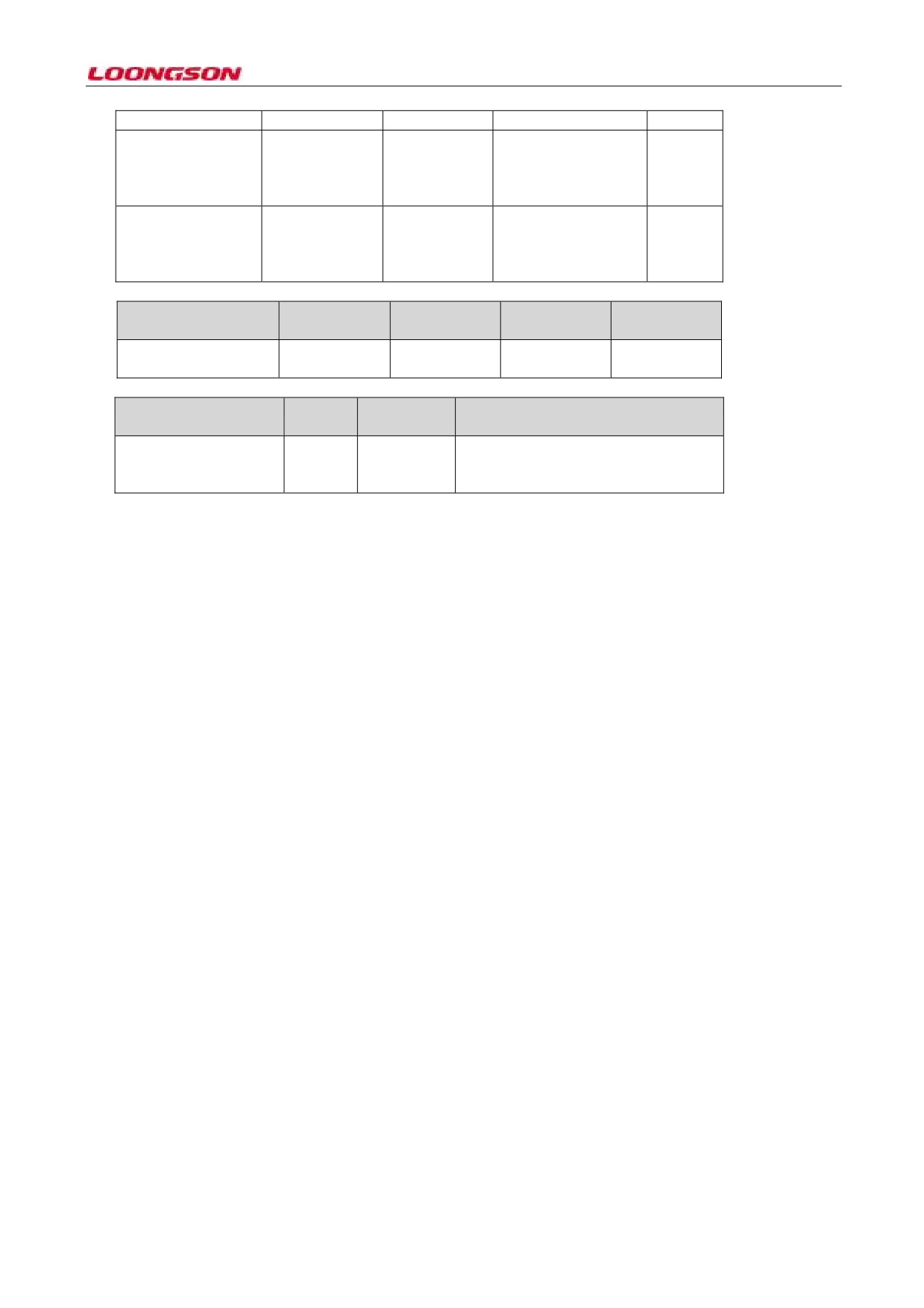
INT0_CLR
INT4_POL
0xbfd0_10b0
R/W
Interrupt
polarity
0x0
selection register 4
In common with
INT0_POL
INT4_EDGE
0xbfd0_10b4
R/W
Interrupt
edge
0x0
selection register 4
In common with
INT0_EDGE
Register name
Address
Read / Write
Function
Reset value
(R / W)
description
INT4_SR
0xbfd0_10a0
R
Interrupt status0x0
register 4
INT4_SR
Bit
Default
Description
values
GPIO[95:64]
31:0
0
GPIO[95:64] is as interrupt input,
interrupt status
Bit
-41-
6 SDRAM Controller
6.1 Overview
The SDRAM memory controller integrated by Loongson
1C processor implement general memory
read/write/sleep operations, support 8/16bit data width, and the maximum capacity is 1GB (1C2 supports 2GB).
6.2 Register Description
SDRAM has one 64bit configuration register SD_CONFIG[63:0], and the effective one is
[41:0]. The
configuration register of system allocation is SD_CONFIG [63:0] and the address is 0x0410~0x0414. It’s defined
as follows:
Register name
Address
Read /
Function description
Reset value
Write (R / W)
SD_CONFIG[31:0]
0xbfd0_0410
R/W
SDRAM parameter configuration0x00143803
register
SD_CONFIG[63:32]
0xbfd0_0414
R/W
SDRAM parameter configuration0x80000080
register
SD_CONFIG
Bit
Default values
Description
CONFIG_VALID
41
Valid configuration register
HANG_UP
40
Flag suspended bit
DEF_SEL
39
Adopt default configuration
TWR
38:37
Precharge time of grains after writing
TREF
36:25
Auto refresh period of grains
TRAS
24:21
Minimum line opening time of grains
TRFC
20:17
Auto refresh time of grains
TRP
16:14
Precharge time of grains
TCL
13:11
Data reading delay of grains
TRCD
10:8
Delayed line command to list command of grains
SD_BIT
7:6
Bit width of grains
SD_CSIZE
5:3
3'h0
Column numbers of grains
SD_RSIZE
2:0
3'h0
Line numbers of grains
6.3 Software Configuration Description
SD_CONFIG register is defined as follows:
1. SD_RSIZE, SD_CSIZE
The effective value of SD_RSIZE is 00, 01, 10 and 11 which correspond to 2K, 4K, 8K and 16K respectively.
The effective value of SD_CSIZE is 00, 01, 10, 11 and 111 which correspond to 512, 1K, 2K, 4K and 256
respectively.
Above two configurations need to correspond to particles, and the column number is larger than line number. Thus
the effective configuration is:
Column/line
00
01
10
11
00
2Kx512
4Kx512
8Kx512 (not common)
16Kx512 (not common)
01
2Kx1K
4Kx1K
8Kx1K
16Kx1K (not common)
-42-
10
No
4Kx2K
8Kx2K
16Kx2K
11
No
No
8Kx4K
16Kx4K
111
2Kx256
4Kx256
8Kx256 (not common)
16Kx256 (not common)
2. SD_BIT
The effective value of SD_BIT is 00, 01 and 10 which correspond to 8bit, 16bit and 32bit respectively.
3. TRCD, TCL, TRP, TRFC, TRAS, TREF, TWR
These particles are related to the physical characteristics of particles, and are physical time which needs
converting into cycle number based on frequency. Some parameters of typical frequency value are listed as
follows:
Parameters
/
150
133
100
75
33
Frequency (MHZ)
TRCD
3
3
2
2
1
TCL
3
3
3
2
2
TRP
3
3
2
2
1
TRFC
9
8
6
5
2
TRAS
7
6
5
4
2
TREF
'h926
'h818
'h620
'h494
'h204
TWR
2
2
2
1
1
4. DEF_SEL
When the bit is 1, it adopts the default configuration (133MHZ configuration). When the bit is 0, it adopts the
external input configuration. When the default configuration is adopted, the register configuration of external
input is ineffective.
5. HANG_UP
When the bit is 1, it notifies that the controller enters in the suspende state, and after completing the operation in
array, SDRAM enters into the sleep state, and exit from the sleep state after HANG_UP is 0. When it exits from
the sleep state, it needs to refresh all lines by at least 240~480us. SD_CONFIG register only has one bit under
normal work.
6. CONFIG_VALID
When the bit is 1, the register configuration is effective; when the bit is 1, it’s recommended to configure
parameters first, and then set 1 bit high.
Notes: In the configuration of two registers, the low bit 0x410 must be written first, and then high 0x414. Or,
when the SDRAM controller is writing 0x414, 0x410 initialization data will be seen as configuration parameter,
and 0x410 data written later will be ineffective. In this way, SDRAM configuration is wrong and can’t work
normally. It’s recommended to write the register three times, and the highest bit is set to 1 last time, and register
enable is configured. (Valid bit in 0x414)
-43-
7 SRAM Controller
7.1 Overview
SRAM memory controller integrated by Loongson 1C processor is multiplexed with SDRAM pin, which support
32MB at most, and 8/16bits data width. SRAM controller can be used in IO device in the same interface sequence
with SRAM.
7.2 Configuration Register
There is only one internal configuration register, and its configuration is shown as follows:
Register name
Address
Read / Write
Function
Reset value
(R / W)
description
MISC_CTRl[15:0]
0xbfe6_4024
R/W
SRAM
0x0004
parameter
configuration
register
SRAM_CTRL
Bit
Default values
Description
SRAM_EN
15
0x0
SRAM enable. When the bit is 1, SDRAM interface is
used as SRAM. When the bit is 0, it’s used as SDRAM
interface.
reserved
14:8
0x0
It must be 0 if reserved
SRAM_WIDTH16
7
0x0
ROM operation data with. When the bit is
1, it
indicates 16 bits. When the bit is 0, it indicates 8 bits.
ROM_INIT_CNT
6:2
0x21
The count initial of RAM operation is used to adjust
the phase of output signal, and ranges from 0 to 0x1f.
CLOCK_PERIOD
1:0
0x0
The count step value of SRAM operation is used to
adjust the time length of adjusting output signal and
operation speed.
00: Stepping at 1, the slowest
01: Stepping at 2
10: Stepping at 4
11: Stepping at 8, the fastest
-44-
8 Camera Interface
8.1 Overview
Camera Interface supports the input of ITU-R BT.601/656 YCbCr 8-bit standard and RGB565/888 8-bit standard.
The input video frequency is 640x480 and 320x240 and any other pixel modes. It supports the zomming out by
one time in 640x480 resolutions in RGB565\888 and ITU-R BT.601 modes. The rest pixel doesn’t support the
zooming out, and there is the output in the format of yuv4:2:2/rgb565/rgb888/rgb0888 by choice.
Functional characteristics of Camera interface controller includes:
Ɣ It supports the external interface of ITU-R BT.601/656 8-bit and RGB565/RGB888 8-bit modes.
ƔSupport configuration by any resolution input;
Ɣ Only 640x480 supports the zooming out by one time.
Ɣ Output format: YCbCr 4:2:2, RGB565, RGB888 and RGB0888 (32bits). When the output format is RGB565/ YCbCr
4:2:2, the input pixels must be integral times of 32; the output format is RGB888/RGB0888, and the input pixel is
integral times of 16.
Ɣ It supports the input of ITU-R BT.601/656 8-bit in any pixel into the output in the format of RGB (565/0888), and
doesn’t support the conversion of RGB input into YCbCr4:2:2 output;
Ɣ The output area has four sections, each of which can accommodate the address space of one frame image, and can
configure the base address of address space, offset address of u and v component storage in the format of YCbCr4:2:2
Ɣ It support the conversion of RGB565 into RGB565;
Ɣ It support the conversion of RGB888 into RGB888 and RGB0888;
Ɣ It support the conversion of BT601 into RGB565, RGB0888 and YUV;
Ɣ It supports the conversion of BT656 into RGB565, RGB0888 and YUV;
Ɣ It supports the zooming out by one time of 640*480 pixel (except the format of TU-R BT.656);
Ɣ It supports the matrix display of the output in the format of RGB.
Interface block diagram of the module:
-45-
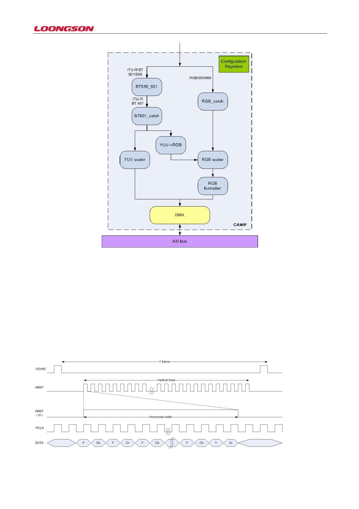
Figure 8-1 Camera interface (CAMIF) functional diagram
8.2 Interface Protocol
PCLK: 1bit input signal; Camera processor driven pixel clock.
VSYNC: 1bit input signal; Camera processor driven frame sync signal.
HREP: 1bit input signal; Camera processor driven frame sync signal.
DATA: 8bit input signal; pixel data initiated by Camera processor.
ITU-R BT.601 8-bit input sequence is shown in Figure 1. Therein, the data input sequence may be YCbY Cr or
YCrYCb or CrYCbY or CbYCrY.
RGB565/RGB888 8-bit input sequence and ITU-R BT.601 8-bit input sequence are consistent, and the data input
sequence is different. For RGB888, the data input sequence may be R G B or B G R. For RGB565, the data input
sequence may be R5G3 G3B5 or B5G3 G3R5. RGB565/RGB888 and ITU-R BT.601 input mode can set the line
effective and frame effective high and low levels based on low two bits of status register.
Figure 8-2 ITU-R BT.601 input sequence
-46-
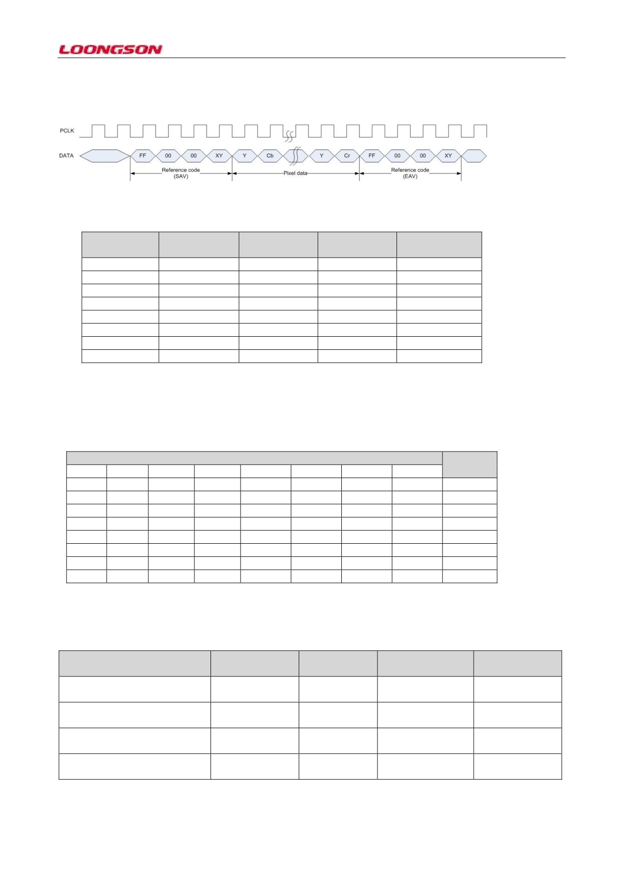
ITU-R BT.656 input sequence is shown in Figure 8-3. Therein, the data input sequence can be Y CbYCr or
YCrYCb or CrYCbY or CbYCrY. SAV is the line start code, and EAV is end code. The definition of reference
code is shown in Table 8-1, and the definition of XY value is shown in Table 8-2. Only when XY is 80, 9D
combination or C7, DA combination, it’s effective line data.
Figure 8-3 ITU-R BT.656 input sequence
Table 8-1 ITU-R BT.656 reference code
Data bit number
The first
The second
The third
The fourth
character (3FF)
character (000)
character (000)
character (XYZ)
7(MSB)
1
0
0
1
6
1
0
0
F
5
1
0
0
V
4
1
0
0
H
3
1
0
0
P3
2
1
0
0
P2
1
1
0
0
P1
0
1
0
0
P0
In Field 1, F is 0; in Field 2, it’s 1.
V other positions 0; vertical blanking interval is 1
H is 0 in SAV and 1 in EAV.
P0, P1, P2, P3: protection byte (see Table 8-2)
Table 8-2 The fourth byte XY value
MSBLSB
XY16 hex
1
F
V
H
P3
P2
P1
P0
1
0
0
0
0
0
0
0
80
1
0
0
1
1
1
0
1
9D
1
0
1
0
1
0
1
1
AB
1
0
1
1
0
1
1
0
B6
1
1
0
0
0
1
1
1
C7
1
1
0
1
1
0
1
0
DA
1
1
1
0
1
1
0
0
EC
1
1
1
1
0
0
0
1
F1
8.3 Register Description
The configuration of the configuration register of base address of frame buffer DMA_ADDRi_CONFIG (i=0,...,3)
is defined as follows:
Register name
Address
Read /
Function
Reset value
Write (R / W)
description
DMA_ADDR0_CONFIG
0x1c280000
R/W
Frame buffer base
32'h0
address 0
DMA_ADDR1_CONFIG
0x1c280008
R/W
Frame buffer base
32'h0
address 1
DMA_ADDR2_CONFIG
0x1c280010
R/W
Frame buffer base
32'h0
address 2
DMA_ADDR3_CONFIG
0x1c280018
R/W
Frame buffer base
32'h0
address 3
-47-
DMA_ADDRi_CONFIG
Bit
Default
Description
values
Frame buffer base address
31:0
32'h0
The software allocates the base address of four buffers, and
the hardware places 4 fame data from address 0 to address 3,
and then address 0 circularly. Each buffer size as a frame
image size. It’s used for DMA to read data and adopts the
physical address.
The configuration of video pixel configuration register CAMIF_CONFIG_PIX is defined as follows. Therein,
except
640x480 and
320x240, the rest video resolution needs to be defined by the configuration of
CAMIF_CONFIG_PIX register.
Register name
Address
Read / Write (R /
Function
Reset value
W)
description
CAMIF_CONFIG_PIX
0xbc280020
R/W
Video resolution32'h0
configuration
register
CAMIF_CONFIG_PIX
Bit
Default
Description
values
Floating pixel resolution line23:12
12'h0
For example, for the pixels of 1280x720, the pixel line
number y
number is configured to 720.
Floating pixel resolution column
11:0
12'h0
For example, for the pixels of 1280x720, the pixel
number x
column number is configured to 1280.
U and V base address configuration register (CAMIF_CONFIG_UOFFSET and CAMIF_CONFIG_VOFFSET) is
defined as follows. The video resolution except 640x480 and 320x240, the configuration buffer needs to specify
the storage base address of U and V components in frame buffer in the format of YUV4:2:2 through base address
configuration register. However, in RGB output display, the offset of CAMIF_CONFIG_UOFFSET configuration
array display address is namely the address interval between lines in an image. For example, the 640x480 image is
displayed in 1280x720 screen, and there are uoffset=(1280-640)x pixel bytes.
Register name
Address
Read / Write (R /
Function
Reset value
W)
description
CAMIF_CONFIG_UOFFSET
0xbc280028
R/W
U base address
32'h0
CAMIF_CONFIG_VOFFSET
0xbc280030
R/W
V base address
32'h0
CAMIF_CONFIG_UOFFSET
Bit
Default
Description
values
U base address configuration
31:0
32'h0
1/2 of frame buffer in the format of YUV4:2:2 is u
register
component
Base address. For example, in
1280x720 resolution,
voffset is decimal 1280x720, and the unit is byte.
CAMIF_CONFIG_VOFFSET
Bit
Default
Description
values
V base address configuration
31:0
32'h0
3/4 of frame buffer in the format of YUV4:2:2 is u
register
component
Base address. For example, in
1280x720 resolution,
voffset is decimal 1280x720 x3/2, and the unit is byte.
CAMIF_CONFIG configuration is the control register of starting and closing camera module, and is defined as
follows:
Register name
Address
Read /
Function
Reset value
-48-
Write (R / W)
description
CAMIF_CONFIG
0xbc280038
R/W
Status register
32'h0
CAMIF_CONFIG
Bit
Default values
Description
CONFIG_PARA_CLR
31:31
1'b0
1: Start CAMERA
0: Close CAMERA
CONFIG_BUF_FULL
23:20
4'b0
Four frame buffers from low to high
1: filled
0: never written or writing
CONFIG_PARA_H_WD
19:16
4'b0
Wait valid Hsync delay beats
CONFIG_PARA_OUTPU
14:13
2'b0
0: YUV422
T_D ATA_MODE
1: RGB565
2: RGB888
3: RGB0888
CONFIG_PARA_INPUT_
12:11
2'b0
0: RGB
DAT A_MODE
1: ITU-R BT.601
2: ITU-R BT.656
CONFIG_PARA_SCALE
10:9
2'b0
0: no scaling
_MO DE
1: zoom out by one time. When the pixel is configurable,
it’s configured to 0.
CONFIG_PARA_640X48
8:7
2'b0
0: 320x240
0
1: 640x480
2: Configurable pixels
CONFIG_PARA_SINGL
6:6
1'b0
1: Single field
EFIE LDEN
0: Non-single field (frame mode with 0)
CONFIG_PARA_YUV_O
5:4
2'b0
Permutation format of YUV422
RDE R
0: YCbYCr
1: YCrYCb
2: CrYCbY
3: CbYCrY
CONFIG_PARA_BGR_E
3:3
1'b0
1: RGB is arranged as BGR
N
0: RGB is arranged as RGB (the conversion of ITU-R
BT.601/656 into RGB is effective)
CONFIG_PARA_RGB_F
2:2
1'b0
0: Input format of RGB is 565
ORM AT
1: Input format of RGB is 888
CONFIG_PARA_HS
1:1
1'b0
1: HSYNC active low
0: HSYNC active high
CONFIG_PARA_VS
0:0
1'b0
1: VSYNC low active
0: VSYNC high active
Notes: when the input format is ITU-R BT.656, Config_para_hs, Config_para_vs is only configured to 0.
8.4 Configuration Operations
8.4.1 Memory Accessing Mode
Output data of Camera interface controller, and its frame memory hierarchy is as follows:
The frame memory of CAMIF output consists of four cyclic memory spaces. For YCbCr output, each memory
space consists of three memory spaces: brightness Y, chroma Cb and Cr. The start address of yuv3 component
storage correspond to base address, 1/2 address and 3/4 address in space; for RGB output, each memory space
stores each RGB pixel in sequence.
The storage mode of output data of Camera interface controller in memory is as follows: Storage mode of little
endian is adopted in frame storage. AXI bus width is 64-bit. When the output is in the format of YCbCr, each Y or
Cb or Cr has one byte, and is arranged in each corresponding area of frame address; when the output is RGB565,
each pixel has two bytes; when the output is RGB888 (32bits), each pixel has four bytes; when the output is
-49-
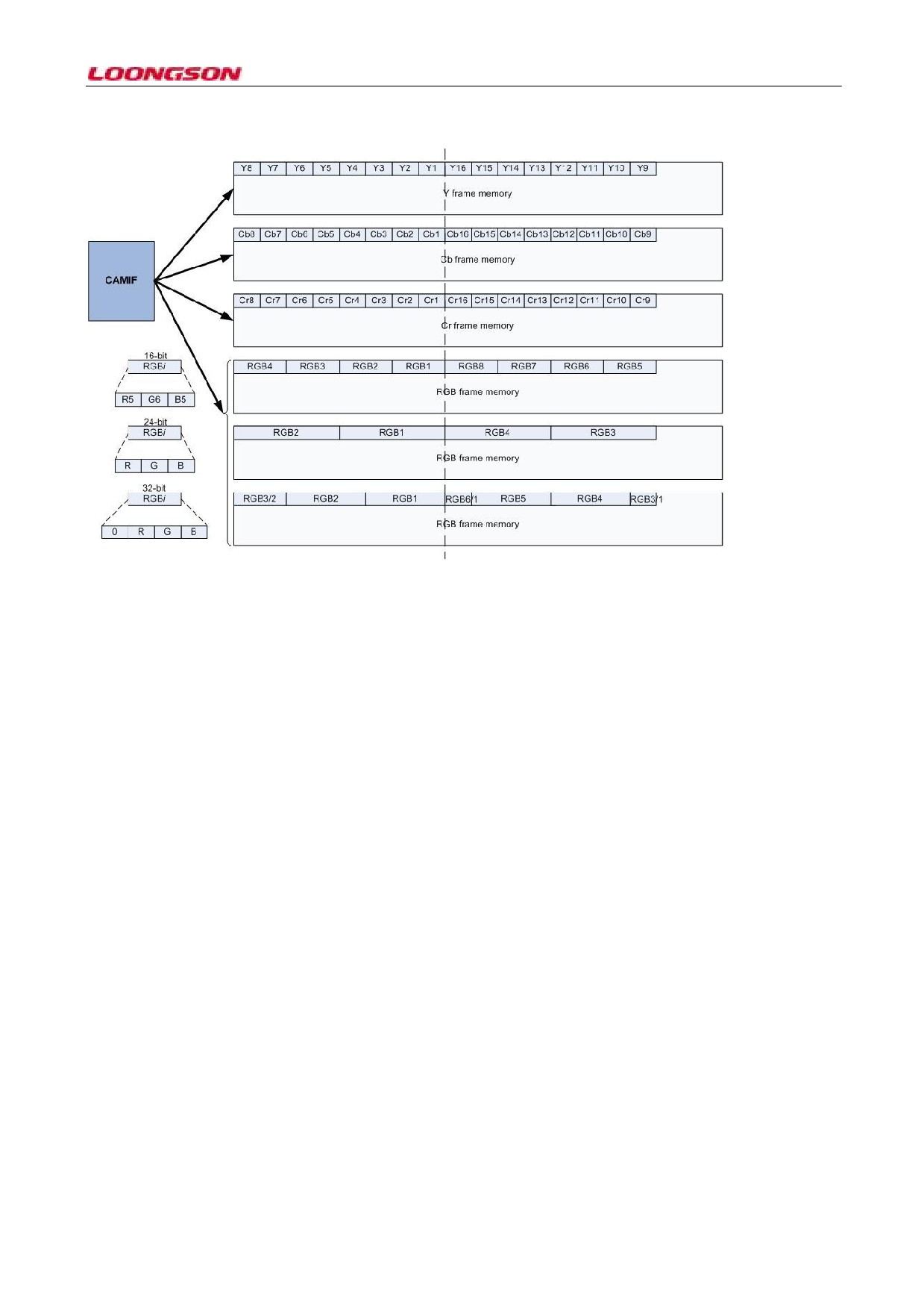
RGB888 (24bits), each pixel has three bytes. As is shown in Figure 8-4.
Figure 8-4 Storage mode
8.4.2 Configuration order
Before operation, CAMERA interface needs to configure some registers based on different conversion modes, and
after the system reset, the register is default value. Only after the register configuration, can the module work. The
working procedures of configuring CAMERA interface are as follows:
1. Read the status register message of Camera interface and obtain the 30th bit. When the bit is 1, it indicates the
inside DMA is under idle status, and the following work configurations can be conducted. It’s because DMA
needs to interact with memory, and when we control the CAMERA interface work and stop, DMA can’t stop in
real time.
2. In working configuration, the base addresses of four address spaces to be stored are configured first. If for any
pixel configuration and the output of YUV format, U and V addresses are required. Finally, the status register is
configured, and its 31st bit is configured to 1, and then it can start work.
3. During work, CAMERA interface will send an interrupt to CPU after filling out one frame address space or
covering the data in DMA module buffer. After the software receives the interrupt, the 23-20 and 28bit of status
register can be inquired. The above 5 bits are all 0 in booting Camera interface, and then become 1 from high to
low after filling out 23-20bits of one frame address space. When filling out one frame address space, the bit
corresponding to the space becomes 0, and the software can query the status register to judge the storage of frame
address space. When the data is covered, 28bit will be set to 1.
4. When the software wants to stop the operation of Camera interface, the 31st bit of the status register needs
writing to 1. Under such circumstance, the Camera interface will stop analyzing the input in Camera, and DMA
will stop sending any data to frame address space. After receiving all sent request responses, the 30th bit of the
status register is set to 1.
5. When the application software of Camera interface is interrupted by other interrupts, the configuration request
of closing Camera interface is added to interrupt hander. Restart it after waiting for recovery (firstly, the 31st bit of
the status register is written to 0, and then 30th value is read. When the bit is 1, 1 is written to the 29th bit. And then
the 30th bit is read, when the bit is 0, 1 is written to the 31st bit). Don’t close Camera interface, and judge the stored
information of frame address space and accept or reject the image based on the information of status register.
-50-
9 I2S Controller
9.1 Overview
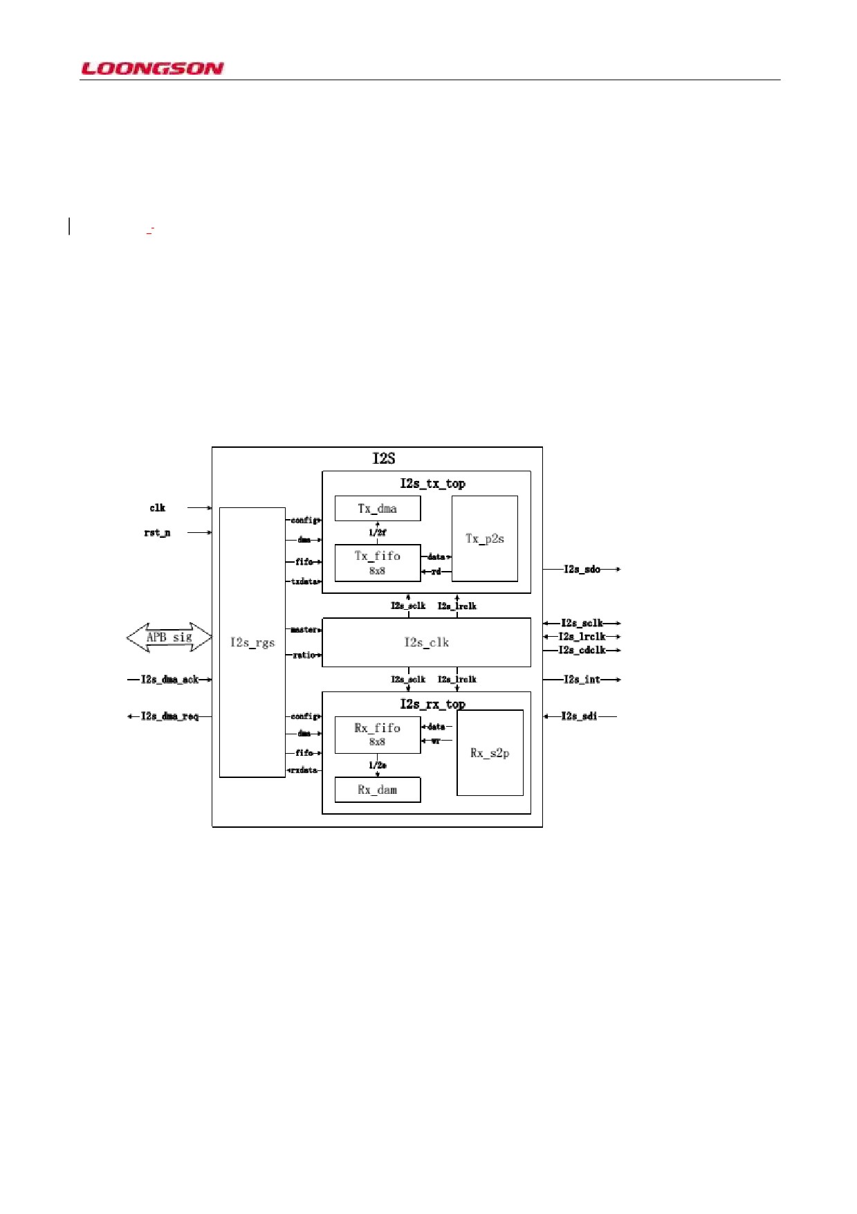
Via APB interface, the data width of I2S controller in 1C is 32 bits, and it supports DMA transmission and several
companies’' codec chip. I2S controller only supports the master mode, and I2S generates bit clock signal and left
and right sound channel selection clock signal.
I2S features include:
Ɣ It supports the audio data sampling bit width of 8, 16, 20, 24 and 32.
Ɣ It supports the left and right sound channel processing word width of 8, 16, 20, 24 and 32.
Ɣ It includes two buffer FIFOs, and the buffer capacity of FIFO is 8 bytes.
Ɣ The interrupt processing mode of I2S is configurable, and after I2S transmit and receiver interrupt functions are
enabled, if it needs to write when the buffer fifo of two channel is full, and or it needs to read when the buffer fifo
is empty, send the interrupt signal to CPU.
Ɣ I2S can provide the system clock for codec chip and the clock frequency is configurable. Interface block diagram of
the module:
Figure 9-1 I2S interface block diagram
9.2 Interface Protocol
The operating time sequence of I2S receiver and transmitter is shown in Figure 9-2. The transmit operation
sequential routine in the format of I2S of the receiver and transmitter is that the next frame data are transmitted in
the 2nd bit clock after the signal selection signal changes, and the data transmits MSB bit first and then LSB bit.
The bit width processed by receiver and transmitter may be inconsistent, and if the bit width of the data
transmitted by transmitter is shorter than that of the supported data, LSB fill zero and send them. Or, some LSB
data may be ignored; similarly, for receiver, when the bit width of the received data is smaller than that processed
by it, LSB will fill zero and send them. Or, some LSB data may be ignored. Thus, for the received data, MSB is
fixed, but LSB depends on the word length of the data to be received and transmitted, and the word length bit
width configured by system.
-51-
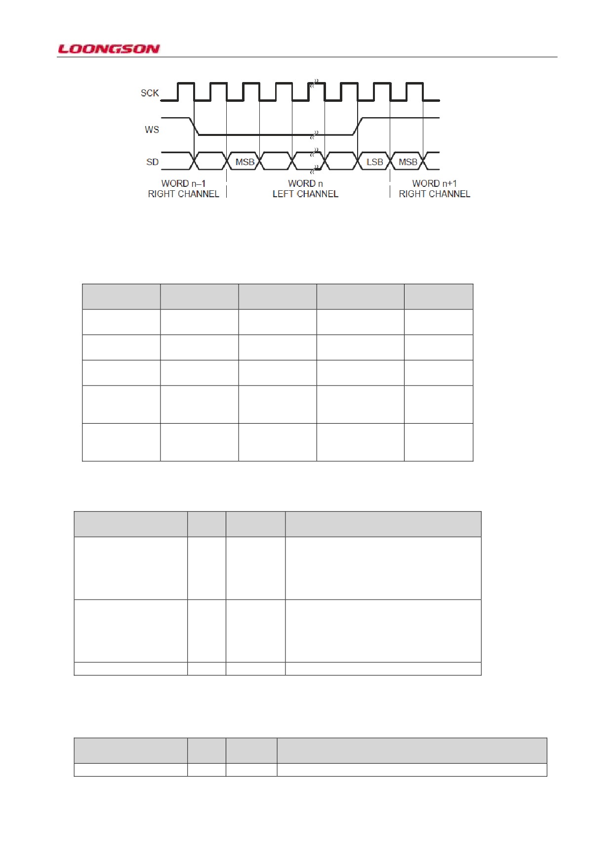
Figure 9-2 I2S transmission protocol
9.3 Dedicated Register
I2S includes five registers, and is as defined by the figure below.
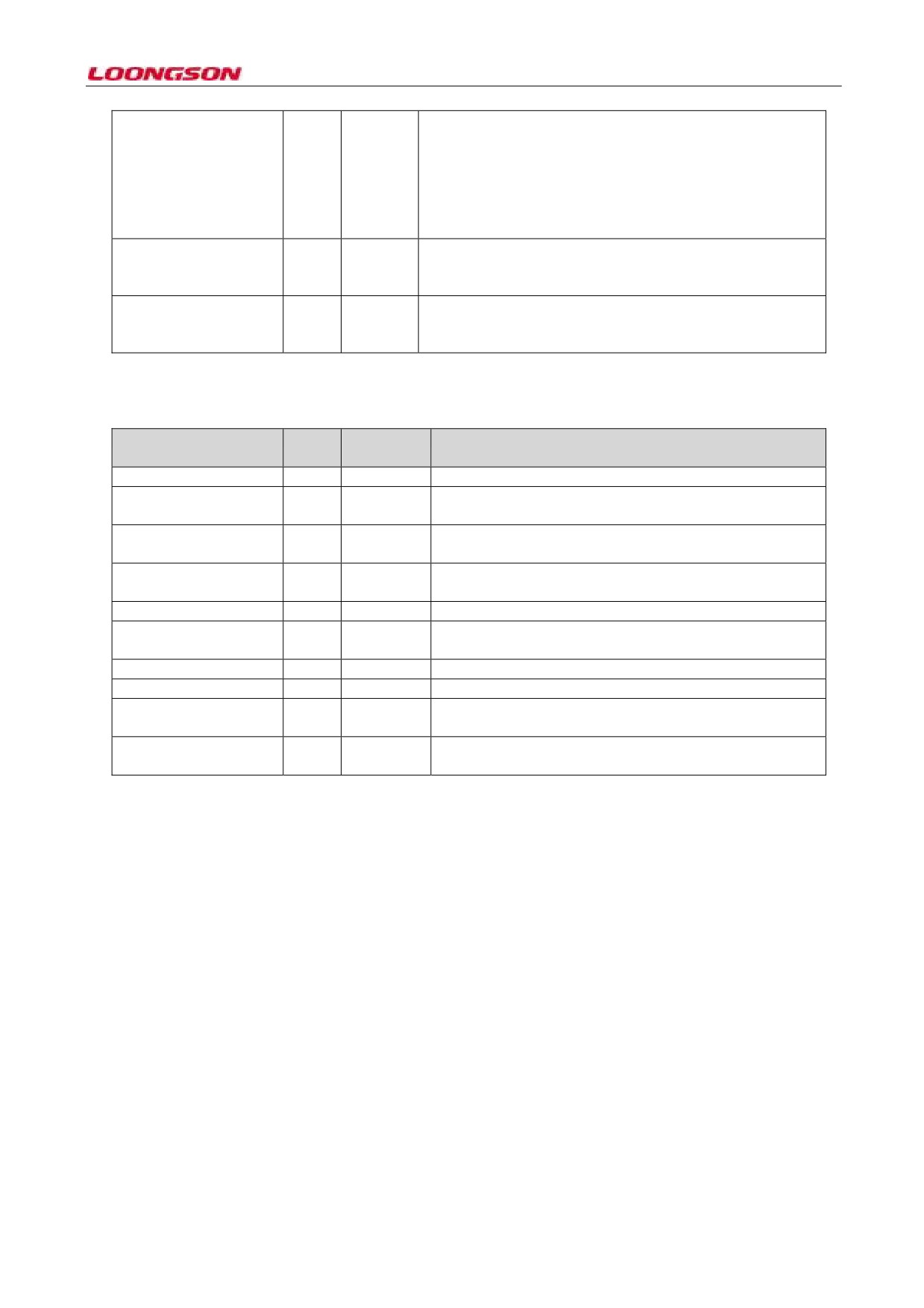
Register name
Address
Read / Write (R
Function
Reset value
/ W)
description
IISVersion
0xbfe6_0000
R/W
I2S
identify32'h0
register
IISConfig
0xbfe6_0004
R/W
I2S configuration32'h0
register
IISControl
0xbfe6_0008
R/W
I2S
control32'h0
register
IISRxData
0xbfe6_000c
R/W
I2S receive data
register
(used for
DMA receive data)
32'h0
IISTxData
0xbfe6_0010
R/W
I2S transmit data
register
(used for
DMA send data)
32'h0
The receive flag register allows the main control computer to read relevant operation information of the receiver.
It identifies the address bit width of IIS, data bit width and version number.
IISVersion
Bit
Default
Description
values
ADRW
9:8
2'h0
Address bus width:
00: Address width 8-bit
01: Address width 16-bit
10: Address width 32-bit
11: Address width 64-bit
DATW
5:4
2'h0
Data width
00: Address width 8-bit
01: Address width 16-bit
10: Address width 32-bit
11: Address width 64-bit
VER
3:0
4'h0
I2S version number
The receive configuration register configures the sound channel word length of I2S, the sampling depth of video
data, and frequency division factor of each clock.
IISConfig
Bit
Default
Description
values
LR_LEN
31:24
'h0
Word length handled by left and right sound tracks.
-52-
RES_DEPTH
23:16
'h0
Sampling depth settings:
IIS sampling data length, effective scope of 8-32. If the
transmitted or received data width is smaller than sampling
data length,
0 is filled to low bit; if the transmitted or
received data width is larger than sampling data length, the
low bit is ignored.
SCLK_RATIO
15:8
'h0
Bit clock (BCLK) frequency coefficient:
Bit clock frequency division factor, frequency division
number is the bus clock frequency divided by 2x(RATIO+1)
MCLK_RATIO
7:0
'h0
System clock (MCLK) frequency division factor, system
clock frequency division factor. The frequency division
number is the bus clock frequency divided by 2x(RATIO+1)
The control register is used to configure the operation enable signal of IIS, buffer the store status of FIFO and
relevant information state of information.
IISControl
Bit
Default
Description
values
MASTER
15
'h0
1: IIS working in master mode
MSB LSB
14
'h0
1: High-order on the left end
0: High-order on the right end
RX_EN
13
'h0
When the bit of controller receive enable is
1, it’s
effective and starts to receive data.
TX_EN
12
'h0
When the bit of controller transmit enable is
1, it’s
effective and starts to transmit data.
RX_DMA_EN
11
'h0
DMA receiver enable, valid at 1
Reserved
10: 8
'h0
TX_DMA_EN
7
'h0
DMA transmitter enable, valid at 1
Reserved
6:2
'h0
RX_INT_EN
1
'h0
When the bit of RX interrupt enable is 1, it’s enable
interrupt. And when the bit is 0, it’s forbidden.
TX_INT_EN
0
'h0
When the bit of TX interrupt enable is 1, it’s enable
interrupt. And when the bit is 0, it’s forbidden.
9.4 Configuration Operations
For the normal operation of I2S, it’s necessary to firstly configure CODEC chip, and then configuration register
and control register of I2S controller.
1C chip communicates through I2C interface and CODEC chip. For CODEC chip as the slave device in I2C bus,
detailed address, register and configuration method, please refer to the data manual of CODEC chip. After the
configuration of CODEC, it’s necessary to configure I2S controller. Some configuration messages are written to
label register (I2SVersion) for search. First configure I2SConfig register, and then I2SControl register.
I2Sconfig register suggests that the configuration of LR_LEN and RES_DEPTH is the same, to avoid lost data or
empty data during transmission. Based on the sampling frequency, sampling depth and frequency multiplying
factor of CODEC, BCK clock is calculated via the formula below:
BCK = 256xfs (or
512xfs) or
(768xfs);
(see CODEC manual recommended configuration in details)
BCK_RATIO= Freq_SDRAM / (256 x fs) /2-1;
The computational formula is as follows if in dual-channel:
SCK = RES_DEPTH x 2 xfs;
SCK_RATIO= Freq_SDRAM / (RES_DEPTH x 2 x fs) /2 - 1;
Wherein fs is the configured sampling frequency. In transmitting and reading data, DMA is configured first and
then controller to avoid lost data. See Section 14.3 for the configuration method of DMA multiplexing
-53-
10 Display Controller (DC)
10.1 Overview
Display controller fetches the frame buffer output from memory to external display interface.
The characteristics supported by display controller of Loongson 1C include:
ƔOne-way DVI display, it supports 1024x768@60Hz at most.
ƔFive data formats: RGB444, RGB555, RGB565, RGB888, RGB8888
Ɣ Output dithering and gamma correction
10.2 Register Definition and Description
10.2.1 Frame buffer configuration register
Register name
Address
R/W
Description
Reset value
frameBufferConfi g
0xbc30_124
R/W
Frame buffer configuration 32’h0
0
register
frameBufferConfi g
bit
Description
Initial value
Reset
20
Soft reset when the value is changed into 0 from 1
0
Gamma
12
Write 1 enable gamma correction
0
Output Enable
8
Write 1 enable display output
0
Format
2:0
Color depth format:
0
0: none
1: RGB444
2: RGB555
3: RGB565
4: RGB888
5: RGB8888
10.2.2 Frame buffer address register 0
Register name
Address
R/W
Description
Reset value
frameBufferAddr0
0xbc301260
R/W
Frame buffer address register 0
32’h0
frameBufferAddr0
bit
Description
Initial value
Address
31:0
Physical address of buffer 0 in memory
0
10.2.3 Frame buffer address register 1
Register name
Address
R/W
Description
Reset value
frameBufferAddr1
0xbfe51580
R/W
Frame buffer address register 1
32’h0
frameBufferAddr1
bit
Description
Initial value
Address
31:0
The physical address of buffer 1 in memory (it0
needs to be the same with frame buffer address
register 0)
10.2.4 Frame buffer span register
Register name
Address
R/W
Description
Reset value
frameBufferStride
0xbc301280
R/W
Frame buffer span register
32’h0
frameBufferStride
bit
Description
Initial value
Stride
31:0
Display the number of bytes in buffer line.
0
When the format of RGB888 (24bit) is used,
stride needs to round up to an integer based on
120 bytes.
When the format of RGB8888 (32bit) is used,
-54-
stride needs to round up to an integer based on
128 bytes.
10.2.5 Color dithering configuration register
Register name
Address
R/W
Description
Reset value
ditherConfig
0xbc301360
R/W
Color dithering configuration32’h0
register
ditherConfig
bit
Description
Initial value
Enable
31
Write 1 enable color dithering function
0
RedSize
19:16
Red domain width
0
GreenSize
11:8
Green domain width
0
BlueSize
3:0
Blue domain width
0
10.2.6 Color vibrance lookup table low-bit register
Register name
Address
R/W
Description
Reset value
ditherTableLow
0xbc301380
R/W
Color dithering lookup
table32’h0
low-bit register
ditherTableLow
bit
Description
Initial value
Y1_X3
31:28
Comparison value at coordinate (3,1)
0
Y1_X2
27:24
Comparison value at coordinate (2.1)
0
Y1_X1
23:20
Comparison value at coordinate (1.1)
0
Y1_X0
19:16
Comparison value at coordinate (0.1)
0
Y0_X3
15:12
Comparison value at coordinate (3.0)
0
Y0_X2
11:8
Comparison value at coordinate (2.0)
0
Y0_X1
7:4
Comparison value at coordinate (1.0)
0
Y0_X0
3:0
Comparison value at coordinate (0.0)
0
10.2.7 Color dithering lookup table high-bit register
Register name
Address
R/W
Description
Reset value
ditherTableHigh
0xbc3013a0
R/W
Color dithering lookup
table32’h0
high-bit register
ditherTableLow
bit
Description
Initial value
Y3_X3
31:28
Comparison value at coordinate (3.3)
0
Y3_X2
27:24
Comparison value at coordinate (2.3)
0
Y3_X1
23:20
Comparison value at coordinate (1.3)
0
Y3_X0
19:16
Comparison value at coordinate (0.3)
0
Y2_X3
15:12
Comparison value at coordinate (3.2)
0
Y2_X2
11:8
Comparison value at coordinate (2.2)
0
Y2_X1
7:4
Comparison value at coordinate (1.2)
0
Y2_X0
3:0
Comparison value at coordinate (0.2)
0
10.2.8 Color dithering description
The function of color dithering is used to enhance the pixel value based on certain rules. In the below example, the
implementation procedures of color dithering function will be explained.
Firstly, to determine which data to enhance (namely, 1 is added to the data bit), and it’s necessary to configure
register Display Dither Configuration. For example, the configuration RedSize is 6 (between 1 and 8, including 1
and 8), it indicates enhancing the 6th bit in MSB bit, namely, the RedColor[2] of RedColor[7:0] is enhanced. It’s
also true of GreenSize and BlueSize.
Secondly, it’s necessary to build the lookup table, namely, configuration register Display Dither Table. The lookup
table includes 16 items, namely, 16 thresholds, and four bit width for each item.
The lookup table is indexed through the lowest 2 bits x[1:0] of x-coordinate and the lowest 2 bits y[1:0] of
y-coordinate of screen pixel counter, and one threshold U[3:0] is obtained.
-55-
The lowest four bits of the pixel corresponding to screen (x, y) location is compared with the found threshold.
If RedColor[3:0] > U[3:0] and RedColor[7:2] isn’t 6 ’b111111, 1 is added to RedColor[2] bit, and the color is
enhanced.
10.2.9 LCD panel configuration register
Register name
Address
R/W
Description
Reset value
panelConfig
0xbc3013c0
R/W
LCD panel configuration register
32’h101
panelConfig
bit
Description
Initial value
ClockPol
9
Clock polarity, write 1 negation
0
ClockEn
8
Clock enable, write 1 enable
1
DEPol
1
Data enable polarity, write 1 negation
0
DE
0
Data enable, write 1 enable
1
10.2.10 Horizontal display width register
Register name
Address
R/W
Description
Reset value
HDisplay
0xbc3014a0
R/W
Horizontal display width register
32’h0
HDisplay
bit
Description
Initial value
Total
27:16
Total pixel number of one display line (including0
non-display area)
Display
11:0
The number of pixels in the display area of the0
display screen line
10.2.11 Line synchronization configuration register
Register name
Address
R/W
Description
Reset value
HSync
0xbc301400
R/W
Line
synchronization32’h40000000
configuration register
HSync
bit
Description
Initial value
Pol
31
Line synchronization polarity, write 1 negation
0
Pulse
30
Line synchronization enable, write 1 enable
1
End
27:16
The number of pixels at the end of the line0
synchronization
Start
11:0
The number of pixels at the start of the line0
synchronization
10.2.12 Vertical display height register
Register name
Address
R/W
Description
Reset value
VDisplay
0xbc301480
R/W
Vertical display height register
32’h0
VDisplay
bit
Description
Initial value
Total
26:16
total pixel number of one display column0
(including non-display area)
Display
10:0
The number of pixels in the display area of the0
display screen column
10.2.13 Field synchronization configuration register
Register name
Address
R/W
Description
Reset value
VSync
0xbc3014a0
R/W
Field
synchronization32’h40000000
configuration register
VSync
bit
Description
Initial value
Pol
31
Field synchronization polarity, write 1 negation
0
Pulse
30
Field synchronization enable, write 1 enable
1
-56-
End
26:16
The number of pixels at the end of the field0
synchronization
Start
10:0
The number of pixels at the start of the field0
synchronization
10.2.14 Output sequencing
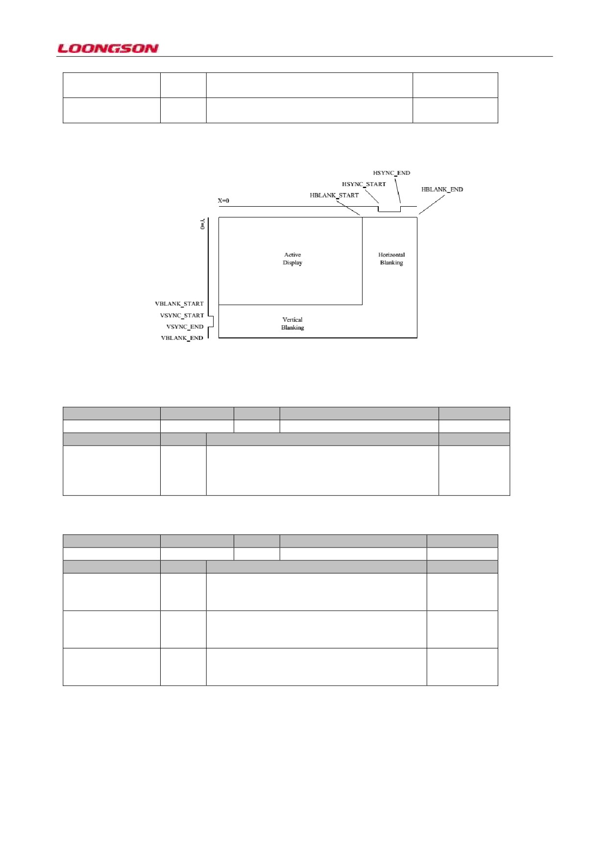
Figure 10-1 Display controller output sequencing
10.2.15 Gamma correction catalog register
Register name
Address
R/W
Description
Reset value
GammaIndex
0xbc3014a0
R/W
Gamma correction catalog register
32’h0
GammaIndex
bit
Description
Initial value
Index
7:0
It indicates Gamma adjustment from which option in0
color values of 0-255, and it’s generally set to 0. It’s
only configured one time, and later the hardware will
automatically increase the value.
10.2.16 Gamma correction value register
Register name
Address
R/W
Description
Reset value
GammaData
0xbc301500
R/W
Gamma correction value register
32’h0
GammaIndex
bit
Description
Initial value
Red
23:16
The red area of Gamma adjustment. The value0
indicated by Gamma Index is adjusted to the value
of the current domain
Green
15:8
The green area of Gamma adjustment. The value0
indicated by Gamma Index is adjusted to the value
of the current domain
Blue
7:0
The blue area of Gamma adjustment. The value0
indicated by Gamma Index is adjusted to the value
of the current domain
10.2.17 Gamma correction instructions
The Gamma adjustment module includes three lookup tables, one responsible for red, one for green, and one for
blue.
Lookup table can be rewritten by register. Lookup table can only be written.
One Gamma adjustment is as follows: (primary color, adjustment color) In the setup of Gamma color lookup table,
the register should be configured in the sequence of color value.
-57-