Loongson 1C300 Processor User Manual (Version 1.0, 2014) - page 2
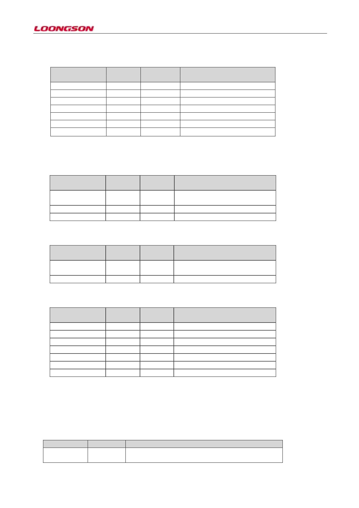
2.16 USB Port
Signal name
Type
Pull-up/
Description
pull-down
USB_DVDD
USB digital power
USB_DVSS
USB digital ground
USB_VDD33
USB analog power supply
USB_VSS33
USB analog ground
USB_REXT
USB reference resistor
USB_DP
DIFF I/O
-
USB differential signal line D +
USB_DM
DIFF I/O
-
USB differential signal line D -
[Notes] In QFP100 package, USB HOST can’t be used. In QFP176 package, it can be used.
2.17 RTC Interface
Signal name
Type
Pull-up/pull-
Description
down
RTC_CLK_I
I
-
RTC oscillator input, connect 32.768K
oscillator
RTC_CLK_O
O
-
RTC crystal oscillator output
VR_VDDA
RTC power supply
2.18 Clock Configuration Signal
Signal name
Type
Pull-up/pull-
Description
down
XTALI
I
-
System clock crystal oscillator input,
connect to 24M
XTAL0
O
-
System clock crystal oscillator output
2.19 Power Ground
Signal name
Type
Pull-up/pull-
Description
down
PLL_ VDD33
P
Core PLL analog power supply
PLL_ VSS33
G
Core PLL analog ground
PLL_VDD12
P
Core PLL digital power supply
PLL_VSS12
G
Core PLL digital ground
CORE_VDD
P
Core voltage power supply
CORE_VSS
G
Core voltage ground
IO_VDD
P
IO power supply
2.20 Initialization Signal
Loongson 1C has three starting modes: SPI FLASH, NAND FLASH and SDIO. Multiplex function pin obtains
the configuration message from the pull-up and pull-down values during system reset for the software to judge the
powered state.
Table 2-1 Configuration signal
Pin name
Signal name
Description
NAND_D [3:0]
start_freq
CPU PLL frequency configuration in hardware control mode
The frequency calculation formula shall be:
-18-

Freq = 6*(4*NAND_D[3:0] + 40)
NAND_D [5:4]
boot_sel
Boot selection is different in QFP100 and QFP176 packages
(in QFP100 packages, the control signal of NAND isn’t
bonded to the pin)
In QFP100 package, boot_sel is
00: Reserved
01: it indicates the boot from SPI flash
10: it indicates the boot from NAND flash
(multiplex
SDRAM pin)
11: it indicates the boot from NAND flash (multiplex MAC
pin)
In QFP176 packaging, boot_sel is
00: Reserved
01: it indicates the boot from SPI flash
10: it indicates the boot from NAND flash
11: it indicates the boot from SDIO
NAND_D [7:6]
nand_type
In NAND boot, configure the capacity of NAND flash
00: it indicates that the capacity is equal to 2Gb (2KB page)
01: it indicates that capacity is 1Gb (2KB page)
10: it indicates that the capacity is 512Mb (512 Bytes page)
11: it indicates the capacity is low and equal to 256MB (512
Bytes page)
NAND_CLE
rs_rd_cfg
In NAND boot, whether to adopt ECC, select NAND only in
boot_sel
Flash valid at startup
When the bit is 0, it indicates the non-ECC boot of NAND
When the bit is 1, it indicates the ECC boot of NAND
SPI0_CLK
usb_refclksel
Clock selective signal of USB_HOST and USB_OTG
When the bit is 1, it indicates the clock is provided by PLL.
When the bit is 0, it indicates the clock is provided by
external oscillator.
-19-
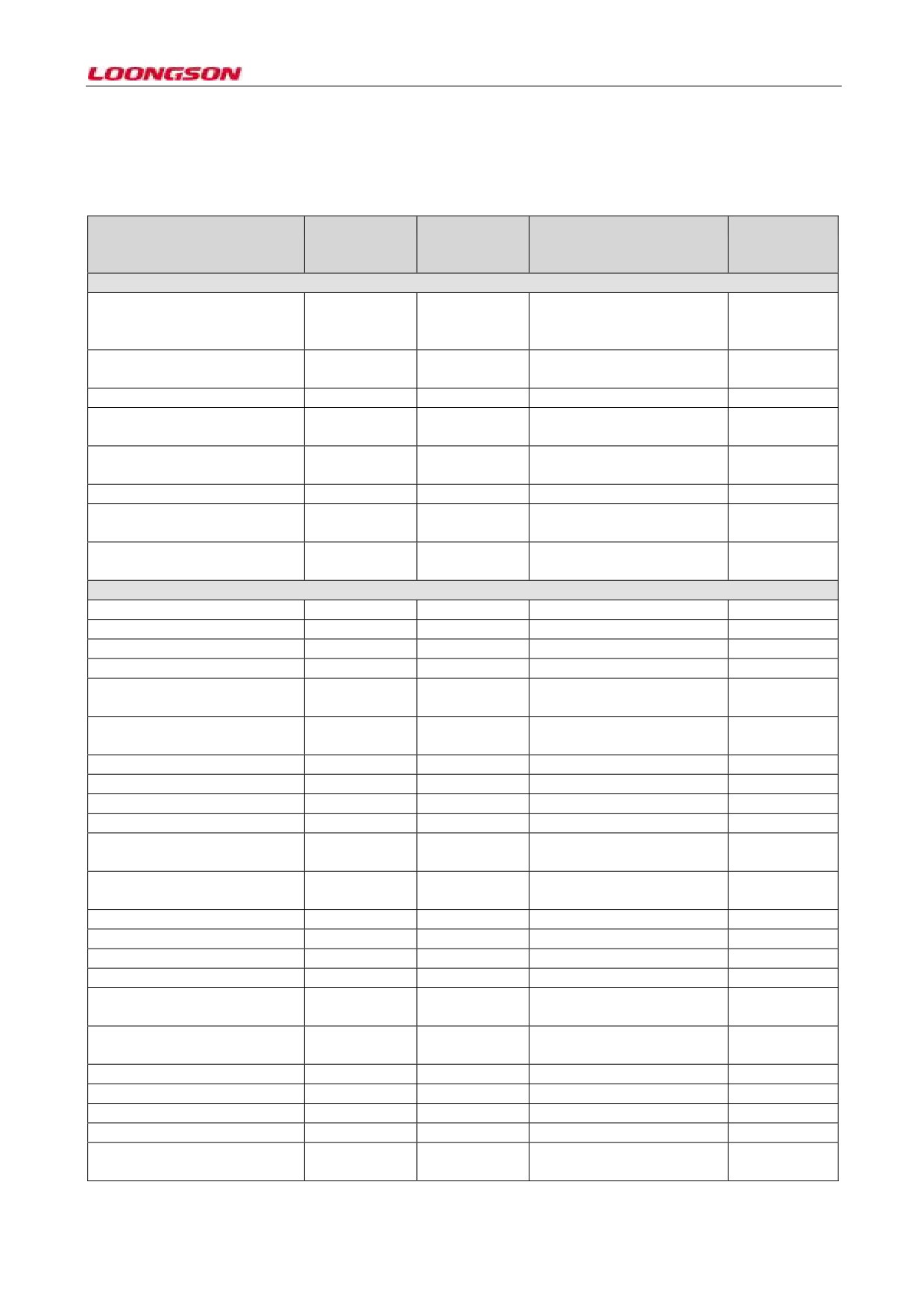
3 Register Definition
3.1 Base Register Definition
Register name
Address
RW
Function description
Reset value
(read/write)
(R/W)
Base register
START_FREQ
0xbfe7_8030
R/W
PLL frequency configurationCharged state
and SDRAM frequency
division factor
CLK_DIV_PARAM
0xbfe7_8034
R/W
CPU/CAMERA/DC
0x0
frequency division factor
CBUS_CONFSIGNALS
0xbfd0_0400
R/W
0x0
CBUS_SD_CTRL0
0xbfd0_0410
R/W
SDRAM
parameter
0x001438a3
configuration register
CBUS_SD_CTRL1
0xbfd0_0414
R/W
SDRAM
parameter
0x80000080
configuration register
SHUT_CTRL
0xbfd0_0420
R/W
Each module switch register
0x0
MISC_CTRL
0xbfd0_0424
R/W
Function
multiplexing0x4
register 0
0xbfe7_c010
CPU dynamic frequency
cpu_throt
R/W
reduction register
0x0
Interrupt register
INTISR0
0xbfd0_0140
R
Interrupt status register 0
0x0
INTEN0
0xbfd0_0144
R/W
Interrupt enable register 0
0x0
INTSET0
0xbfd0_0148
R/W
Interrupt setting register 0
0x0
INTCLR0
0xbfd0_014c
R/W
Interrupt clear register 0
0x0
INTPOL0
0xbfd0_0150
R/W
Interrupt triggering level flag
register 0
0x0
INTEDGE0
0xbfd0_0154
R/W
Interrupt triggering edge flag
register 0
0x0
INTISR1
0xbfd0_0158
R
Interrupt status register 1
0x0
INTEN1
0xbfd0_015c
R/W
Interrupt enable register 1
0x0
INTSET1
0xbfd0_0160
R/W
Interrupt setting register 1
0x0
INTCLR1
0xbfd0_0164
R/W
Interrupt clear register 1
0x0
INTPOL1
R/W
Interrupt triggering level flag
0xbfd0_0168
register 1
0x0
INTEDGE1
R/W
Interrupt triggering edge flag
0xbfd0_016c
register 1
0x0
INTISR2
0xbfd0_0170
R
Interrupt status register 2
0x0
INTEN2
0xbfd0_0174
R/W
Interrupt enable register 2
0x0
INTSET2
0xbfd0_0178
R/W
Interrupt setting register 2
0x0
INTCLR2
0xbfd0_017c
R/W
Interrupt clear register 2
0x0
INTPOL2
R/W
Interrupt triggering level flag
0xbfd0_0180
register 2
0x0
INTEDGE2
R/W
Interrupt triggering edge flag
0xbfd0_0184
register 2
0x0
INTISR3
0xbfd0_0188
R
Interrupt status register 3
0x0
INTEN3
0xbfd0_018c
R/W
Interrupt enable register 3
0x0
INTSET3
0xbfd0_0190
R/W
Interrupt setting register 3
0x0
INTCLR3
0xbfd0_0194
R/W
Interrupt clear register 3
0x0
INTPOL3
R/W
Interrupt triggering level flag
0xbfd0_0198
register 3
0x0
-20-
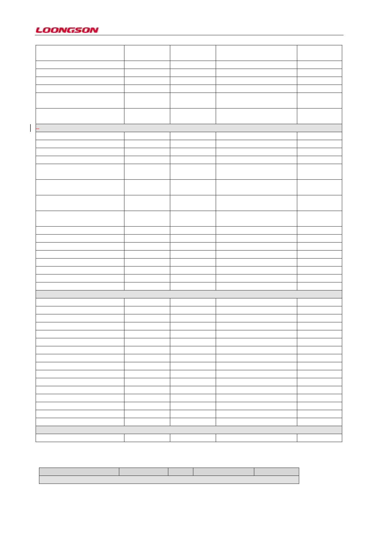
INTEDGE3
R/W
Interrupt triggering edge flag
0xbfd0_019c
register 3
0x0
INTISR4
0xbfd0_01ª0
R
Interrupt status register 4
0x0
INTEN4
0xbfd0_01ª4
R/W
Interrupt enable register 4
0x0
INTSET4
0xbfd0_01ª8
R/W
Interrupt setting register 4
0x0
INTCLR4
0xbfd0_01ac
R/W
Interrupt clear register 4
0x0
INTPOL4
R/W
Interrupt triggering level flag
0xbfd0_01b0
register 4
0x0
INTEDGE4
R/W
Interrupt triggering edge flag
0xbfd0_01b4
register 4
0x0
GPIO register
GPIO_CFG0
0xbfd0_01c0
R/W
GPIO configuration register 0
0xffe00040
GPIO_CFG1
0xbfd0_01c4
R/W
GPIO configuration register 1
0xfc00_3f3f
GPIO_CFG2
0xbfd0_01c8
R/W
GPIO configuration register 2
0x1ff0_3fff
GPIO_CFG3
0xbfd0_01cc
R/W
GPIO configuration register 3
0x0
GPIO_OE0
R/W
GPIO output enable register 0
0xbfd0_01d0
GPIO_OE1
R/W
GPIO output enable register 1
0xbfd0_01d4
0xfc00_3f3f
GPIO_OE2
R/W
GPIO output enable register 2
0xbfd0_01d8
0x1ff0_3fff
GPIO_OE3
R/W
GPIO output enable register 3
0xbfd0_01dc
0x0
GPIO_IN0
0xbfd0_01e0
R/W
GPIO input register 0
0x0
GPIO_IN1
0xbfd0_01e4
R/W
GPIO input register 1
0x0
GPIO_IN2
0xbfd0_01e8
R/W
GPIO input register 2
0x0
GPIO_IN3
0xbfd0_01ec
R/W
GPIO input register 3
0x0
GPIO_OUT0
0xbfd0_01f0
R/W
GPIO output register 0
0x0
GPIO_OUT1
0xbfd0_01f4
R/W
GPIO output register 1
0x0
GPIO_OUT2
0xbfd0_01f8
R/W
GPIO output register 2
0x0
GPIO_OUT3
0xbfd0_01fc
R/W
GPIO output register 3
0x0
Multiplexed relationship register
CBUS_FIRST0
0xbfd0_11c0
R/W
First multiplexed register 0
0x0
CBUS_FIRST1
0xbfd0_11c4
R/W
First multiplexed register 1
0x0
CBUS_FIRST2
0xbfd0_11c8
R/W
First multiplexed register 2
0x0
CBUS_FIRST3
0xbfd0_11cc
R/W
First multiplexed register 3
0x0
CBUS_SECOND0
0xbfd0_11d0
R/W
Second multiplexed register 0
0x0
CBUS_SECOND1
0xbfd0_11d4
R/W
Second multiplexed register 1
0x0
CBUS_SECOND2
0xbfd0_11d8
R/W
Second multiplexed register 2
0x0
CBUS_SECOND3
0xbfd0_11dc
R/W
Second multiplexed register 3
0x0
CBUS_THIRD0
0xbfd0_11e0
R/W
Third multiplexed register 0
0x0
CBUS_THIRD1
0xbfd0_11e4
R/W
Third multiplexed register 1
0x0
CBUS_THIRD2
0xbfd0_11e8
R/W
Third multiplexed register 2
0x0
CBUS_THIRD3
0xbfd0_11ec
R/W
Third multiplexed register 3
0x0
CBUS_FOURTH0
0xbfd0_11f0
R/W
Fourth multiplexed register 0
0x0
CBUS_FOURTH1
0xbfd0_11f4
R/W
Fourth multiplexed register 1
0x0
CBUS_FOURTH2
0xbfd0_11f8
R/W
Fourth multiplexed register 2
0x0
CBUS_FOURTH3
0xbfd0_11fc
R/W
Fourth multiplexed register 3
0x0
DMA configuration register
ORDER_ADDR_IN
0xbfd0_1160
R/W
DMA configuration register
3.2 Each Module Register Definition
Register name
Address
R/W
Function description
Reset value
SDRAM interface
-21-
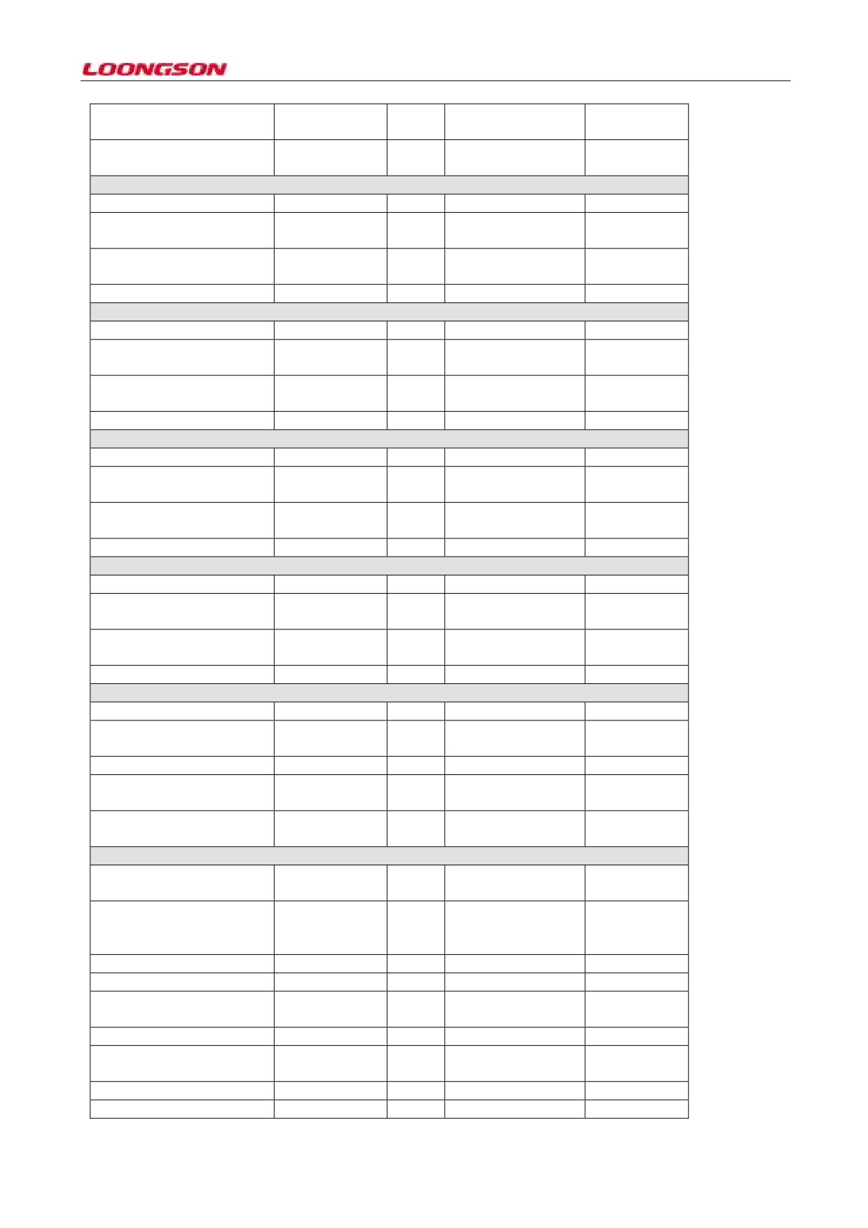
SD_CONFIG[31:0]
0xbfd0_0410
R/W
SDRAM parameter
0x30d0db5a
configuration register
SD_CONFIG[63:32]
0xbfd0_0414
R/W
SDRAM parameter
0x50
configuration register
PWM0
CNTR
0xbfe5_c000
R/W
Basic counter
0x0
HRC
0xbfe5_c004
R/W
High pulse timing0x0
reference register
LRC
0xbfe5_c008
R/W
Low pulse timing0x0
reference register
CTRL
0xbfe5_c00c
R/W
Control register
0x0
PWM1
CNTR
0xbfe5_c010
R/W
Basic counter
0x0
HRC
0xbfe5_c014
High pulse timing0x0
R/W
reference register
LRC
0xbfe5_c018
Low pulse timing
0x0
R/W
reference register
CTRL
0xbfe5_c01c
R/W
Control register
0x0
PWM2
CNTR
0xbfe5_c020
R/W
Basic counter
0x0
HRC
0xbfe5_c024
R/W
High pulse timing
reference register
0x0
LRC
0xbfe5_c028
R/W
Low pulse timing
reference register
0x0
CTRL
0xbfe5_c02c
R/W
Control register
0x0
PWM3
CNTR
0xbfe5_c030
R/W
Basic counter
0x0
HRC
R/W
High pulse timing
0xbfe5_c034
reference register
0x0
LRC
R/W
Low pulse timing
0xbfe5_c038
reference register
0x0
CTRL
0xbfe5_c03c
R/W
Control register
0x0
I2S interface
IISVersion
0xbfe6_0000
R/W
I2S identify register
0x0
IISConfig
0xbfe6_0001
R/W
I2S
configuration
0x0
register
IISState
0xbfe6_0002
R/W
I2S status register
0x0
IISRxData
0xbfe6_0003
R/W
I2S data reception
0x0
register
IISTxData
0xbfe6_0004
R/W
I2S data transmission0x0
register
AC97
CSR
0xbfe6_0000
R/W
Configuration status0x0
register
OCC0
R/W
Output
channel0x4141
0xbfe6_0004
configuration register
0
OCC1
0xbfe6_0008
Reserved
OCC2
0xbfe6_000c
Reserved
ICC
R/W
Input
channel
0x410000
0xbfe6_0010
configuration register
CODEC_ID
0xbfe6_0014
Codec ID register
CRAC
Codec register access0x0
0xbfe6_0018
command
OC0
0xbfe6_0020
Output sound track 0
OC1
0xbfe6_0024
Output sound track 1
-22-
OC2
0xbfe6_0028
Reserved
OC3
0xbfe6_002c
Reserved
OC4
0xbfe6_0030
Reserved
OC5
0xbfe6_0034
Reserved
OC6
0xbfe6_0038
Reserved
OC7
0xbfe6_003c
Reserved
OC10
0xbfe6_0040
Reserved
IC0
0xbfe6_0044
Reserved
IC1
0xbfe6_0048
Reserved
IC2
0xbfe6_004c
Input sound track 2
INTRAW
0xbfe6_0054
R/W
Interrupt
status
register
INTM
0xbfe6_0058
R/W
Interrupt mask
0x0
INT_CLR
R
Interrupt status / clear 0x0
0xbfe6_005c
register
INT_OC_CLR
R
OC Interrupt clear 0x0
0xbfe6_0060
register
INT_IC_CLR
R
IC Interrupt clear 0x0
0xbfe6_0064
register
INT_CW_CLR
R
CODEC
write0x0
0xbfe6_0610
interrupt clear register
INT_CR_CLR
R
CODEC read interrupt
0x0
0xbfe6_006c
clear register
RTC
sys_toywrite0
W
TOY low 32-bit value
0xbfe6_4024
read-in
sys_toywrite1
W
TOY high 32-bit value
0xbfe6_4028
read-in
sys_toyread0
R
TOY low 32-bit value
0xbfe6_402C
read-out
sys_toyread1
R
TOY high 32-bit value
0xbfe6_4030
read-out
SDIO interface
sdi_con
0xbfe6_c000
R/W
SDIO control register
0x0
sdi_pre
0xbfe6_c004
R/W
SDIO
prescale
0x1
register
sdi_cmd_arg
0xbfe6_c008
R/W
SDIO
command0x0
parameter register
sdi_cmd_con
0xbfe6_c00c
R/W
SDIO
command
0x0
control register
sdi_cmd_sta
0xbfe6_c010
R
SDIO command status
0x0
register
sdi_rsp0
0xbfe6_c014
R/W
SDIO
response
0x0
register 0
sdi_rsp1
0xbfe6_c018
R/W
SDIO
response
0x0
register 1
sdi_rsp2
0xbfe6_c01c
R/W
SDIO
response
0x0
register 2
sdi_rsp3
0xbfe6_c020
R/W
SDIO
response
0x0
register 3
sdi_dtimer
0xbfe6_c024
R/W
SDIO timing register
0x1388
sdi_bsize
0xbfe6_c028
R/W
SDIO block size
0x0
register
sdi_dat_con
0xbfe6_c02c
R/W
SDIO data control
0x0
register
sdi_dat_cnt
0xbfe6_c030
R/W
SDIO data counter
0x0
-23-
sdi_dat_sta
0xbfe6_c034
R
SDIO data status 0x0
register
sdi_fsta
0xbfe6_c038
R
SDIO FIFO status 0x0
register
sdi_int_mask
0xbfe6_c03c
R/W
SDIO interrupt mask0x0
register
sdi_wdat
0xbfe6_c040
R/W
SDIO (data register)
0x0
sdi_int_en
0xbfe6_c064
RW
SDIO interrupt enable0x0
register
ADC interface
adc_cnt
0xbfe7_4000
R/W
Frequency division0x400010
and sampling interval
register
adc_s_ctrl
0xbfe7_4004
R/W
Single
sampling
0x0
control register
adc_c_ctrl
0xbfe7_4008
R/W
Continuous sampling
0x0
control register
x_range
0xbfe7_4010
R/W
Touch screen X 0x3ff0000
direction threshold
y_range
0xbfe7_4014
R/W
Touch screen Y 0x3ff0000
direction threshold
awatchdog_range
0xbfe7_4018
R/W
Analog
watchdog
0x3f0000f
threshold
axis
0xbfe7_401c
R/W
Touch
screen
0x0
coordinates
adc_s_dout0
0xbfe7_4020
R/W
Result
of
single0x0
sampling by channel
0 and channel 1
adc_s_dout1
0xbfe7_4024
R/W
Result
of
single0x0
sampling by channel
2 and channel 3
adc_c_dout
0xbfe7_4028
R/W
Continuous sampling0x0
results
adc_debounce_cnt
0xbfe7_402c
R/W
Touch
screen0x640
debouncing time
adc_int
0xbfe7_4030
R/W
ADC interrupt flag
0x0
and control
NAND
NAND_CMD
0Xbfe7_8000
R/W
NAND command
0x0
register
ADDR_C
0Xbfe7_8004
R/W
NAND page offset
0x0
address register
ADDR_R
0Xbfe7_8008
R/W
NAND page address 0x0
register
NAND_TIMING
0Xbfe7_800C
R/W
NAND
timing0x412
sequence register
ID_L
0Xbfe7_8010
R
NAND low ID
0x0
register
STATUS & ID_H
0Xbfe7_8014
R
NAND high ID
0x0
register
NAND_PARAMETER
0Xbfe7_8018
R/W
NAND
grain
0x
parameter register
NAND_OP_NUM
0Xbfe7_801C
R/W
NAND reading and0x800
writing
number
register
CS_RDY_MAP
0Xbfe7_8020
R/W
NAND grain RDY
0x0
-24-
Signal
DMA access address
0Xbfe7_8040
R/W
NAND read-write
0x0
data register
CAMERA interface
DMA_ADDR0_CONFIG
0xbc28_0000
R/W
Frame buffer base
0x0
address 0
DMA_ADDR1_CONFIG
0xbc28_0008
R/W
Frame buffer base
0x0
address 1
DMA_ADDR2_CONFIG
0xbc28_0010
R/W
Frame buffer base
0x0
address 2
DMA_ADDR3_CONFIG
0xbc28_0018
R/W
Frame buffer base
0x0
address 3
Camif_config_pix
0xbc28_0020
R/W
Floating
resolution
0x0
ratio pixel
Camif_config_uoffset
0xbc28_0028
R/W
U base address
0x0
Camif_config_voffset
0xbc28_0030
R/W
V base address
0x0
Camif_config
0xbc28_0038
R/W
Status register
0x0
HCNTR interface
hcntr_ctrl
0xbfe7_c000
R/W
Timer control register
0x0
-25-
4 Clock Architecture
4.1 Clock Architecture
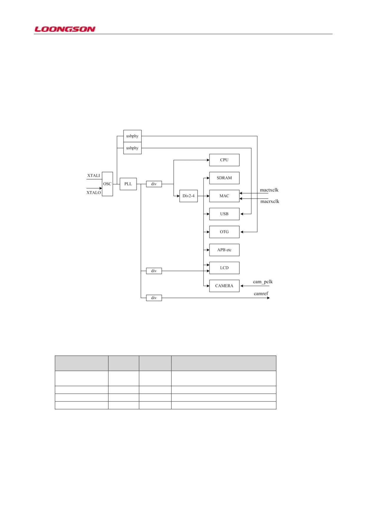
The clock architecture of Loongson 1C is shown in the figure below, and the clock from XTALI/O is sent to two
USBPHY and one PLL. After frequency division, PLL generates the work clock of main modules such as CPU,
SDRAM, MAC and USB; modules such as USB, MAC and OTG use their respective clock in interface (or
reference clock)
Figure 4-1 System clock architecture
4.2 Clock Signal Description
Table 4-1 has introduced all clock pins of Loongson 1C.
Table 4-1 Loongson 1C clock signal
Signal name
Frequency
Type
Description
(Hz)
XTALI XTALO
PLL and USBPHY reference clocks are
I/O
connected to 24MHz crystal.
MACTXCLK
I
MAC reference clock transmission
MACRXCLK
I
MAC reference clock reception
CAM_PCLK
I
Camera pixel clock
-26-
5 Chip Configuration and Control
5.1 Address space allocation
The address space of Loongson 1C is divided into three levels, including the address space of modules above the
first-level AXI crossbar module, that of all modules under AXI_MUX, and that of on-APB modules.
Table 5-1 Space assignment of AXI modules
Address space
Equipment
Note
0x0000_0000 - 0x0fff_ffff
SDRAM
256MB
0xbc28_0000 - 0xbc2f_ffff
CAMERA_IF
512K
0xbc30_0000 - 0xbc3f_ffff
DC
1MB
0xbf00_0000 - 0xbfff_ffff
AXI MUX
16MB
Table 5-2 Address assignment of all AXI modules
Address space
Equipment
Note
0xbd00,0000 - 0xbd7f,ffff
SPI0-memory
8MB
0xbe00,0000 - 0xbe3f,ffff
SPI1-memory
4MB
0xbfc0_0000 - 0xbfcf_ffff
Boot
1MB is mapped to SPI
or NAND by means of
system booting.
0xbfd0_0000 - 0xbfdf_ffff
CONFREG
1MB
0xbfe0_0000 - 0xbfe0_ffff
OTG
64KB
0xbfe1_0000 - 0xbfe1_ffff
MAC
64KB
0xbfe2_0000 - 0xbfe2_ffff
USB
64KB
0xbfe4_0000 - 0xbfe7_ffff
APB-devices
256KB
0xbfe8,0000 - 0xbfeb,ffff
SPI0-IO
256KB
0xbfec,0000 - 0xbfef,ffff
SPI1-IO
256KB
Table 5-3 Address assignment of all AXI modules
Address space
Modules
Note
0xbfe4_0000-0xbfe4_3fff
UART0
16KB
0xbfe4_4000-0xbfe4_7fff
UART1
16KB
0xbfe4_8000-0xbfe4_bfff
UART2
16KB
0xbfe4_c000-0xbfe4_c0ff
UART3
16KB
0xbfe4_c400-0xbfe4_c4ff
UART4
256B
0xbfe4_c500-0xbfe4_c5ff
UART5
256B
0xbfe4_c600-0xbfe4_c6ff
UART6
256B
0xbfe4_c700-0xbfe4_c7ff
UART7
256B
0xbfe4_c800-0xbfe4_c8ff
UART8
256B
0xbfe4_c900-0xbfe4_c9ff
UART9
256B
0xbfe4_ca00-0xbfe4_caff
UART10
256B
0xbfe4_cb00-0xbfe4_cbff
UART11
256B
0xbfe5_0000-0xbfe5_3fff
CAN0
16KB
0xbfe5_4000-0xbfe5_7fff
CAN1
16KB
0xbfe5_8000-0xbfe5_bfff
I2C-0
16KB
0xbfe5_c000-0xbfe5_ffff
PWM
16KB
0xbfe6_0000-0xbfe6_3fff
AC97/I2S
16KB
0xbfe6_4000-0xbfe6_7fff
RTC
16KB
0xbfe6_8000-0xbfe6_bfff
I2C-1
16KB
0xbfe6_c000-0xbfe6_ffff
SDIO
16KB
0xbfe7_0000-0xbfe7_3fff
I2C-2
16KB
0xbfe7_4000-0xbfe7_7fff
ADC
16KB
0xbfe7_8000-0xbfe7_bfff
NAND
16KB
-27-
0xbfe7_c000-0xbfe7_ffff
HCNTR
16KB
5.2 Chip Configuration Register (CONFREG)
There is a dedicated configuration register module (CONFREG) in Loongson 1C chip, which is used for some
basic configurations and multiplex relations in chip. The following is a list of registers and instructions.
5.2.1 PLL/SDRAM Frequency configuration register
Register name
Address
R/W
Function description
Reset value
START_FREQ
0xbfe78030
R/W
PLL
Configuration
frequency and
SDRAM
frequency
coefficient
START_FREQ
Bit
Default values
Description
PLL_VALID
31
0
PLL valid bit of clock multiplier factor
Reserved
30:24
0
FRAC_N
23:16
0
PLL fractional part of clock multiplier
factor
M_PLL
15:8
Configured by Integer part of PLL clock multiplier factor
NAND_D [3:0]
(theoretically, it may reach
255, but had
better not exceed 100)
Reserved
7:4
0
RST_TIME
3:2
Resetting time after PLL frequency
configuration completion
00: Indicate no reset
01: Indicate 0x100 CLK
10: Indicate 0x400 CLK
10: Indicate 0xff0 CLK
SDRAM_DIV
1:0
Frequency division factor from CPU to
SDRAM
00: Indicate 2 fractional frequency
01: Indicate 4 fractional frequency
10 or 11: Indicate 3 fractional frequency
Notes: the frequency division factor N of PLL is fixed as 4, and the calculation formula of PLL frequency is
shown as follows:
Freq_PLL = XIN *(M_PLL + FRAC_N)/4
5.2.2 CPU/CAMERA/DC frequency configuration register
Register name
Address
Read / Write
Function description
Reset value
(R / W)
CLK_DIV_PARAM
0xbfe7-8034
R/W
CPU/CAMERA/DC
frequency
division
factor
CLK_DIV_PARAM
Bit
Default
Description
values
PIX_DIV
31:24
0x24
DC frequency coefficient of pixel clock
PIX_DIV[7] is the significant bit value
of configuration parameter. When it’s 1,
PIX_DIV[6:0] is valid.
-28-

PIX_DIV[6:0] is the frequency division
factor. When it’s 0, there is no frequency
division, and it ranges from 1 to 27.
CAM_DIV
23:16
0x24
CAMERA clock frequency coefficient
CAM_DIV[7] is the significant bit of
configuration parameter. When it’s
1,
CAM_DIV[6:0] is valid.
CAM_DIV[6:0] is the frequency
division factor. When it’s 0, there is no
frequency division, and it ranges from 1
to 127.
CPU_DIV
15:8
0x2
CPU clock frequency coefficient
CPU_DIV[7] is the significant bit of
configuration parameter. When it’s
1,
CPU_DIV[6:0] is valid.
CPU_DIV[6:0] is the frequency
division factor. When it’s 0, there is no
frequency division, and it ranges from 1
to 127.
Reserved
7:6
0
PIX_DIV_VALID
5
0
DC pixel clock frequency coefficient
valid
PIX_SEL
4
0
DC pixel clock selection signal
When it’s 1, select fractional frequency
clock
When it’s 0, select the crystal oscillator,
and input clock (bypass mode)
CAM_DIV_VALID
3
0
CAMERA valid clock frequency
coefficient
CAM_SEL
2
0
CAMERA clock selection signal
When it’s 1, select fractional frequency
clock
When it’s 0, select the crystal oscillator,
and input clock (bypass mode)
CAM_DIV_VALID
1
0
CPU valid clock frequency coefficient
CAM_SEL
0
0
CPU clock selection signal
When it’s 1, select fractional frequency
clock
When it’s 0, select the crystal oscillator,
and input clock (bypass mode)
Freq_PIX = Freq_PLL/PIX_DIV;
Freq_CAM = Freq_PLL/CAM_DIV;
Freq_CPU = Freq_PLL/CPU_DIV;
Freq_SDRAM = Freq_CPU/SDRAM_DIV;
5.2.3 SDRAM parameter register
Register name
Address
Read / Write
Function
Reset value
(R / W)
description
SD_CONFIG[31:0]
0xbfd0_0410
R/W
SDRAM
0x001438a3
parameter
configuration
register
SD_CONFIG[63:32]
0xbfd0_0414
R/W
SDRAM
0x80000080
parameter
configuration
-29-
register
See Chapter 7 for instructions and configuration of SDRAM parameter register
5.2.4 SHUT_CTRL register
Register name
Address
Read / Write
Function
Reset value
(R / W)
description
shut_ctrl
0xbfd0_0420
R/W
Each module0x0
switch register
SHUT_CTRL
Bit
Default
Description
values
UART_split
31:30
0
Full-function serial port uart0 partition
scheme.
00: Used as full-function serial port
01: Used as 2 four-wire serial ports
OUTPUT_CLK
29:26
0
Clock output configuration.
Each bit indicates a clock output
When the 0bit is 1, it indicates the
PIX_CLK output of DC; when the 1st
bit is
1, it indicates the CAMERA
clock output from SPI0_CS pin; when
the
2nd bit is
1, it indicates the
CAMERA clock output from PWM0
pin; when the 3rd bit is 1, it indicates
the clock output of crystal clock.
ADC_shut
25
0
ADC module shutdown, valid at 1
SDIO_shut
24
0
SDIO module shutdown, valid at 1
DMA2_shut
23
0
DMA2 module shutdown, valid at 1
DMA1_shut
22
0
DMA1 module shutdown, valid at 1
DMA0_shut
21
0
DMAO module shutdown, valid at 1
SPI1_shut
20
0
SPI1 module shutdown, valid at 1
SPI0_shut
19
0
SPI0 module shutdown, valid at 1
I2C2_shut
18
0
I2C2 module shutdown, valid at 1
In
addition,
for
the
UART0
full-function multiplex configuration
bit, please refer to
5.2.6 UART
multiplex configuration register
I2C1_shut
17
0
I2C1 module shutdown, valid at 1
I2C0_shut
16
0
I2C0 module shutdown, valid at 1
AC97_shut
15
0
AC97 module shutdown, valid at 1
I2S_shut
14
0
I2C module shutdown, valid at 1
UART3_shut
13
0
UART3 module shutdown, valid at 1
UART2_shut
12
0
UART2 module shutdown, valid at 1
UART1_shut
11
0
UART1 module shutdown, valid at 1
UART0_shut
10
0
UART0 module shutdown, valid at 1
CAN1_shut
9
0
CAN1 module shutdown, valid at 1
CAN0_shut
8
0
CAN0 module shutdown, valid at 1
ECC_shut
7
0
NAND ECC function off, and when it’s
1, it’s effective.
MAC_shut
6
0
MAC module shutdown, valid at 1
USBHOST_shut
5
0
USBHOST module shutdown, valid at
1
USBOTG_shut
4
0
USBOTG module shutdown, valid at 1
-30-
SDRAM_shut
3
0
SDRAM module shutdown, valid at 1
SRAM_shut
2
0
SRAM module shutdown, valid at 1
CAM_shut
1
0
CAMERA module shutdown, valid at 1
LCD_shut
0
0
LCD module shutdown, valid at 1
5.2.5 MISC_CTRL register
Register name
Address
Read / Write
Function
Reset value
(R / W)
description
misc_ctrl
0xbfe6_4024
R/W
Multiplexing
function register
MISC_CTRL
Bit
Default
Description
values
USBHOST_RSTn
31
0
USBHOST module software reset
PHY_INTF_SEL_i
30:28
0
MAC module MII interface
configuration signal
000: MII mode
100: RMII mode
Reserved
27:26
0
AC97_EN
25
0
AC97 and I2S multiplex options. When
the bit is 1, AC97 is used. When the bit
is 0, I2S is used.
SDIO_DMA_EN
24:23
0
SDIO uses DMA. When the bit is 0,
DMA isn’t used. When the bit is 1,
DMA0 is used. When the bit is 2,
DMA1 is used. When the bit is 3,
DMA2 is used.
ADC_DMA_EN
22
0
ADC uses DMA, When the bit is 1, it’s
significant.
Reserved
21:18
0
SDIO_USE_SPI1
17
0
SDIO uses SPI1 pin. When the bit is 1,
it’s signifant.
SDIO_USE_SPI0
16
0
SDIO uses SPI0 pin. When the bit is 1,
it’s significant.
SRAM_CTRL
15:0
0
SRAM configuration parameters. See
SRAM.
5.2.6 Cpu_throt register
Register name
Address
Read / Write
Function
Reset value
(R / W)
description
cpu_throt
0xbfe7_c010
R/W
CPU dynamic0x0
downclock
control register
cpu_throt
Bit
Default
Description
values
Reserved
31:4
0
CPU frequency reduction coefficients.
cpu_throt
3:0
0xf
This configuration is only effective for
CPU frequency, and has no influence on
bus clock and SDRAM clock.
cpu_throt is described as follows:
-31-
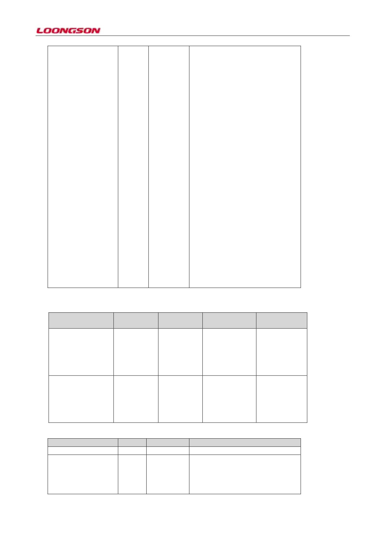
0xf: Keep CPU frequency unchanged.
0xe: Reduce to
15/16 of the
original
frequency
0xd: Reduce to 14/16 of the
original
frequency
0xc: Reduce to
13/16 of the
original
frequency
0xb: Reduce to 12/16 of the
original
frequency
0xa: Reduce to
11/16 of the
original
frequency
0x9: Reduce to 10/16 of the
original
frequency
0x8: Reduce to
9/16
of the
original
frequency
0x7: Reduce to
8/16
of the
original
frequency
0x6: Reduce to
7/16
of the
original
frequency
0x5: Reduce to
6/16
of the
original
frequency
0x4: Reduce to
5/16
of the
original
frequency
0x3: Reduce to
4/16
of the
original
frequency
0x3: Reduce to
3/16
of the
original
frequency
0x1: Reduce to
2/16
of the
original
frequency
0x0: Reduce to
1/16
of the
original
frequency
5.2.7 UART multiplex configuration register
Register name
Address
Read / Write
Function
Reset value
(R / W)
description
uart0_full_func
0xbfd0_0420
R/W
Whether
to
0x0
multiplex
uart4~uart6 into
the full function
or self function of
uart0
uart8_full_func
0xbfe4_c904
R/W
Whether
to
0x0
multiplex
uart9~uart11 into
the full function
or self function of
uart8
UART0_FULL_FUNC
Bit
Default values
Description
31:19
0
misc_ctrl[31:19]
uart0_full_func
18
0
When the bit is 0, uart4~uart6 is used as
the self signal of uart4~6, and I2C2
module is opened.
When the bit is 1, uart4~uart6 is used as
the self signal of uart0, and I2C2 module
-32-
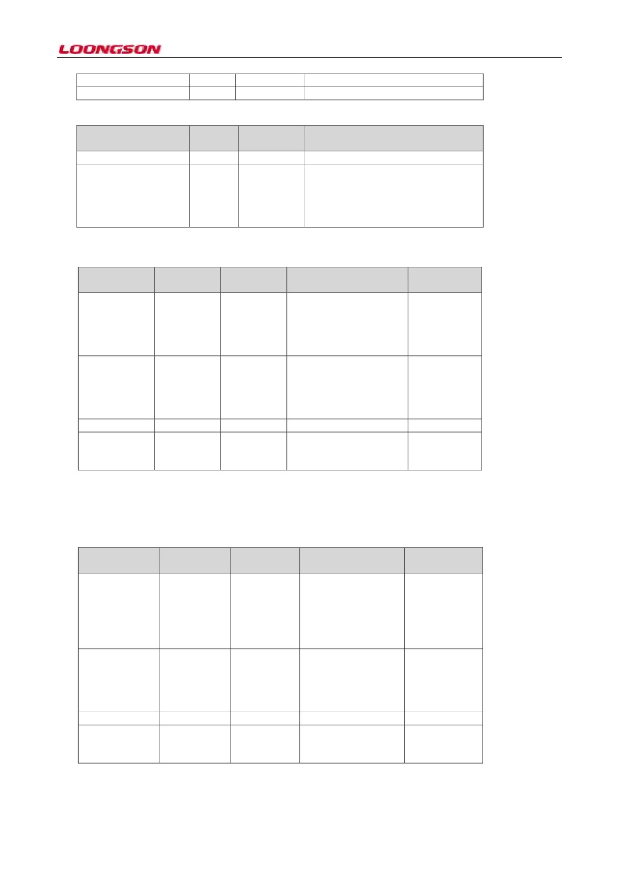
is opened.
17:0
0
misc_ctrl[17:0]
UART8_FULL_FUNC
Bit
Default
Description
values
7:1
0
In common with MSR [7:1]
uart8_full_func
0
0
When the bit is 0, uart9~uart11 is used
as the self signal of uart8~11
When the bit is 1, uart9~uart11 is used
as the self signal of uart8, and I2C2
module is closed.
5.2.8 GPIO0 Configuration Register (corresponding GPIO[31:0])
Register name
Address
Read / Write
Function description
Reset value
(R / W)
GPIO_CFG0
0xbfd0_10c0
R/W
GPIO0 configuration
0xfc00_3f3f
register
1 indicates the
configuration is GPIO,
and 0 indicates ineffective.
GPIO_EN0
0xbfd0_10d0
R/W
GPIO0 output enable
0xfc00_3f3f
register
1 indicates the input, and
0 indicates the
configuration is input.
GPIO_IN0
0xbfd0_10e0
R
GPIO0 input register
0x0
GPIO_OUT0
0xbfd0_10f0
R/W
GPIO0 output register
0x0
High output at 1
Low output at 0
If the GPIO[16] output is configured 1, it’s necessary to configure GPIO_CFG[16] as 1, then GPIO_EN[16] as 1,
and GPIO_OUT[16] as 1. Similarly, GPIO0~GPIO127 input or output can be configured.
5.2.9 GPIO1 configuration register (corresponding GPIO[63:32])
Register name
Address
Read
/ Write
Function description
Reset value
(R / W)
GPIO_CFG1
0xbfd0_10c4
R/W
GPIO1 configuration
0x0
register
1 indicates the
configuration is
GPIO, and 0 indicates
ineffective.
GPIO_EN1
0xbfd0_10d4
R/W
GPIO1 output enable
0x0
register
1 indicates the input,
and 0 indicates the
configuration is input.
GPIO_IN1
0xbfd0_10e4
R
GPIO1 input register
0x0
GPIO_OUT1
0xbfd0_10f4
R/W
GPIO1 output register
0x0
High output at 1
Low output at 0
-33-
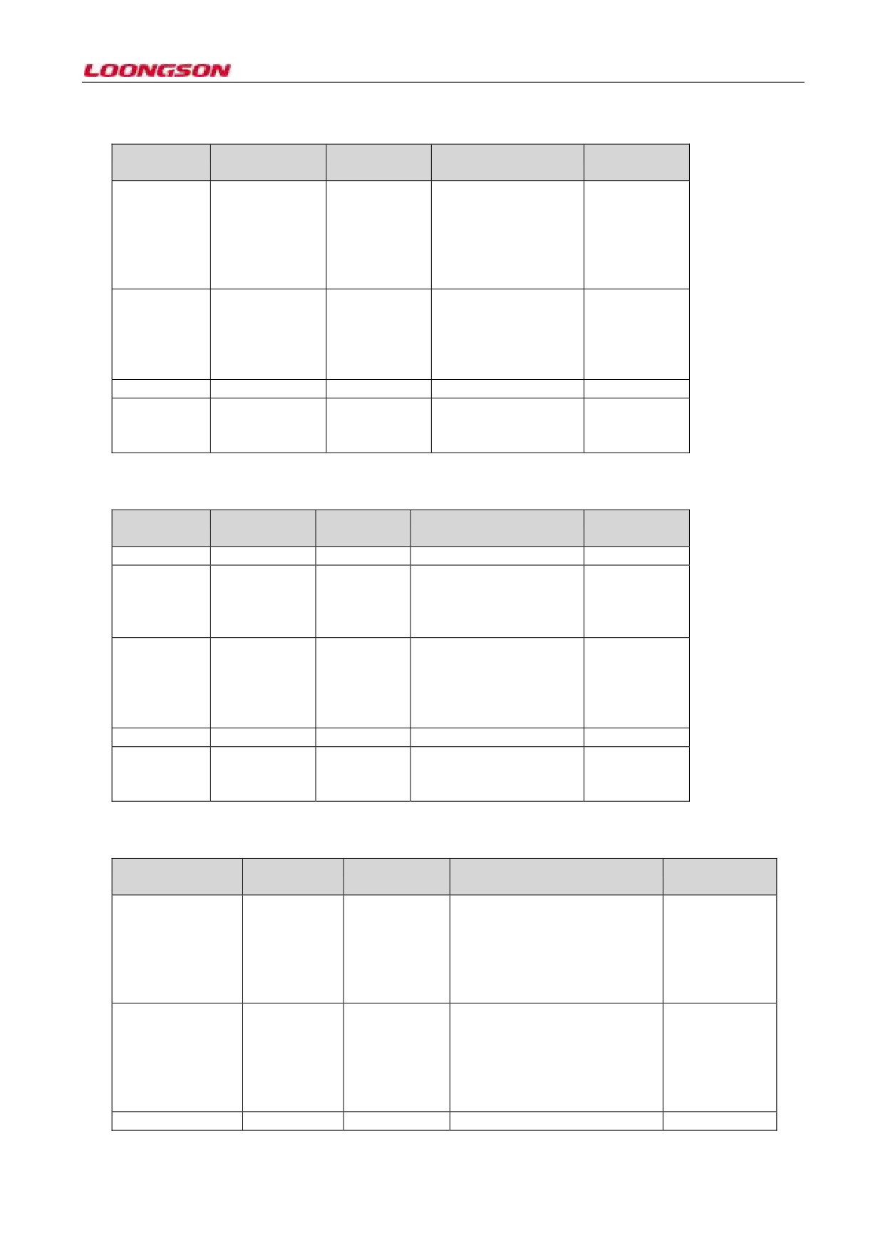
5.2.10 GPIO2 configuration register (corresponding GPIO[95:64])
Register name
Address
Read
/ WriteFunction description
Reset value
(R / W)
GPIO_CFG2
0xbfd0_10c8
R/W
GPIO2 configuration
0x0
register
1 indicates the
configuration is GPIO,
and 0 indicates
ineffective.
GPIO_EN2
0xbfd0_10d8
R/W
GPIO2 output enable
0x0
register
1 indicates the input,
and 0 indicates the
configuration is input.
GPIO_IN2
0xbfd0_10e8
R
GPIO2 input register
0x0
GPIO_OUT2
0xbfd0_10f8
R/W
GPIO2 output register
0x0
High output at 1 and
low output at 0
5.2.11 GPIO3 configuration register (corresponding GPIO[127:96])
Register name
Address
Read / Write
Function description
Reset value
(R / W)
GPIO_CFG3
0xbfd0_10cc
R/W
GPIO3 configuration
0x0
Register
1 indicates the
configuration is GPIO, and
0 indicates ineffective.
GPIO_EN3
0xbfd0_10dc
R/W
GPIO3 output enable
0x0
register
1 indicates the input, and 0
indicates the configuration
is input.
GPIO_IN3
0xbfd0_10ec
R
GPIO3 input register
0x0
GPIO_OUT3
0xbfd0_10fc
R/W
GPIO3 output register
0x0
High output at 1
Low output at 0
5.2.12 PAD[31:0] pin multiplex relation configuration register
Register name
Address
Read /
Function description
Reset value
Write (R / W)
CBUS_FIRST0
0xbfd0_11c0
R/W
PAD[31:0]
1st
multiplex
0x0
register. When the bit is
1, it
indicates the corresponding
PAD is configured as the
1st
multiplex, and when the bit is 1,
it indicates ineffective.
CBUS_SECOND0
0xbfd0_11d0
R/W
PAD[31:0]
2nd
multiplex
0x0
register. When the bit is
1, it
indicates the corresponding
PAD is configured as the 2nd
multiplex, and when the bit is 0,
it indicates ineffective.
CBUS_THIRD0
0xbfd0_11e0
R/W
PAD [31:0] No.
0x0
-34-

The 3rd multiplex register, when
the bit is
1, it indicates the
corresponding
PAD is
configured as the 3rd multiplex,
and when the bit is
0, it
indicates ineffective.
CBUS_FOURTHT0
0xbfd0_11f0
R/W
PAD[31:0]
4th
multiplex
0x0
register. When the bit is
1, it
indicates the corresponding
PAD is configured as the
4th
multiplex, and when the bit is 0,
it indicates ineffective.
CBUS_FIFTHT0
0xbfd0_1200
R/W
PAD[31:0]
5th
multiplex
0x0
register. When the bit is
1, it
indicates the corresponding
PAD is configured as the
5th
multiplex, and when the bit is 0,
it indicates ineffective.
1C chip pin has several multiplex relations, and has six functions and one GPIO multiplex relation at most. See
multiplex relation table in Chapter VII of data book. The multiplexed relationship of each pin is prioritized as
follows:
1st multiplex>2nd multiplex>3rd multiplex>4th multiplex>5th multiplex>GPIO multiplex>default function
For example, to use the 4th multiplex function of PAD[21], it’s necessary to configure CBUS_FIRST0[21]~
CBUS_THIRD0[21] as 0 and CBUS_FOURTH0[21] as 1. If to use default function, it’s necessary to configure
CBUS_FIRST0[21]~ CBUS_FOURTH0[21] and GPIO[21] as 0.
5.2.13 PAD[63:32] pin multiplex relation configuration register
Register name
Address
Read / Write
Function description
Reset value
(R / W)
CBUS_FIRST1
0xbfd0_11c4
R/W
PAD[63:32] the
1st multiplex
0x0
register, bit
When the bit is 1, it indicates
that
corresponding
PAD
configuration
is
the
1st
multiplex. When the bit is 0, it
indicates ineffective.
CBUS_SECOND1
0xbfd0_11d4
R/W
PAD[63:32]
2nd
multiplex
0x0
register. When the bit is 1, it
indicates the corresponding
PAD is configured as the 2nd
multiplex, and when the bit is
0, it indicates ineffective.
CBUS_THIRD1
0xbfd0_11e4
R/W
PAD[63:32]
3rd
multiplex
0x0
register. When the bit is 1, it
indicates the corresponding
PAD is configured as the 3rd
multiplex, and when the bit is0,
it indicates ineffective.
CBUS_FOURTHT1
0xbfd0_11f4
R/W
PAD[63:32]
4th
multiplex
0x0
register. When the bit is 1, it
indicates the corresponding
PAD is configured as the 4th
multiplex, and when the bit is
0, it indicates ineffective.
CBUS_FIFTHT1
0xbfd0_1204
R/W
PAD[63:32]
5th
multiplex
0x0
-35-
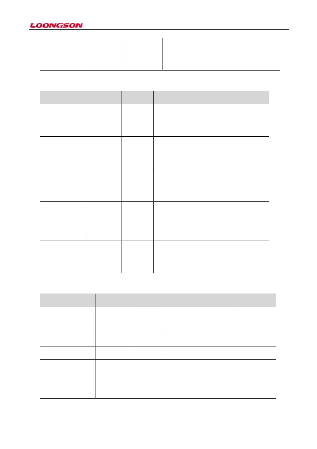
register. When the bit is 1, it
indicates the corresponding
PAD is configured as the 5th
multiplex, and when the bit is
0, it indicates ineffective.
5.2.14 PAD[95:64] pin multiplex relation configuration register
Register name
Address
Read / Write
Function description
Reset value
(R / W)
CBUS_FIRST2
0xbfd0_11c8
R/W
PAD[95:64] 1st multiplex register.
0x0
When the bit is 1, it indicates the
corresponding PAD is configured
as the 1st multiplex, and when the
bit is 1, it indicates ineffective.
CBUS_SECOND2
0xbfd0_11d8
R/W
PAD[95:64] 2nd multiplex register.
0x0
When the bit is 1, it indicates the
corresponding PAD is configured
as the 2nd multiplex, and when the
bit is 0, it indicates ineffective.
CBUS_THIRD2
0xbfd0_11e8
R/W
PAD[95:64] 3rd multiplex register.
0x0
When the bit is 1, it indicates the
corresponding PAD is configured
as the 3rd multiplex, and when the
bit is0, it indicates ineffective.
CBUS_FOURTHT2
0xbfd0_11f8
R/W
PAD[95:64] 4th multiplex register.
0x0
When the bit is 1, it indicates the
corresponding PAD is configured
as the 4th multiplex, and when the
bit is 0, it indicates ineffective.
CBUS_FIFTHT2
0xbfd0_1208
R/W
PAD [95:64] No.
0x0
The 5th multiplex register, when the
bit
is
1,
it
indicates the
corresponding PAD is configured
as the 5th multiplex, and when the
bit is 0, it indicates ineffective.
5.2.15 PAD[127:96] pin multiplex relation configuration register
Register name
Address
Read / Write
Function description
Reset value
(R / W)
CBUS_FIRST3
0xbfd0_11cc
R/W
PAD[127:96]
1st multiplex
0x0
register
CBUS_SECOND3
0xbfd0_11dc
R/W
PAD[127:96]
2nd multiplex
0x0
register
CBUS_THIRD3
0xbfd0_11ec
R/W
PAD[127:96]
3rd multiplex
0x0
register
CBUS_FOURTHT3
0xbfd0_11fc
R/W
PAD[127:96]
4th multiplex
0x0
register
CBUS_FIFTHT3
0xbfd0_120c
R/W
PAD[127:96]
5th multiplex
0x0
register. When the bit is 1, it
indicates the corresponding
PAD is configured as the 5th
multiplex, and when the bit is
0, it indicates ineffective.
-36-
5.3 Interrupt Configuration Register
There are five groups in total in interrupt register which correspond to five interrupt bits in CAUSE register of
CPU. Each group consists of status register, enable register, set register, clear register, level selection register and
edge selection register. Each bit of these five registers is in one-to-one correspondence. All PIO[104:0] can be
used as interrupt status register, and special interrupt register is distributed in INT0_SR and INT1_SR.
The first group of interrupt registers
Register name
Address
Read / Write
Function description
Reset
(R / W)
value
INT0_SR
0xbfd0_1040
R
When the bit of interrupt status
0x0
register 0 is 1, it indicates that the
corresponding
bit
generates
interrupt. When it’s 0, it indicates
no interrupt.
INT0_EN
0xbfd0_1044
R/W
When the bit of interrupt status
0x0
register 0 is 1, it indicates that the
corresponding bit of enable
generates interrupt. When it’s 0, it
indicates it’s forbidden.
INT0_SET
0xbfd0_1048
R/W
When the bit of interrupt status
0x0
register
0 is
1, it indicates the
interrupt setting. When it’s o, it’s
ineffective.
INT0_CLR
0xbfd0_104C
R/W
When the bit of interrupt clear
0x0
register is 1, it indicates clearing
interrupt. When it’s o, it’s
ineffective.
INT0_POL
0xbfd0_1050
R/W
Interrupt polarity selection register
0x0
0
When int0_edge is configured as
the level trigger, the bit 1 indicates
the high level triggered interrupt.
When it’s 0, it indicates the low
level trigger.
When int0_edge is configured as
edge trigger. When it’s
1, it
indicates the up edge trigger
interrupt. When it’s 0, it indicates
the down edge trigger.
INT0_EDGE
0xbfd0_1054
R/W
Interrupt edge selection register 0
0x0
When the bit is 1, it indicates the
edge trigger, and when it’s 0, it
indicates the level trigger.
Register name
Address
Read / Write
Function
Reset value
(R / W)
description
INT0_SR
0xbfd0_1040
R
Interrupt status0x0
register 0
INT0_SR
Bit
Default
Description
values
NAND_int
31
0
NAND interrupt status bit
SDIO_int
30
0
SDIO interrupt status bit
UART3_int
29
0
UART3 interrupt status bit
-37-