LoongArch Reference Manual. Volume 1: Basic Architecture (Version 1.02) - page 5
STLE.D:
vaddr = GR[rj]
AddressComplianceCheck(vaddr)
paddr = AddressTranslation(vaddr)
if GR[rj] <= GR[rk]:
MemoryStore(GR[rd][63:0], paddr, DOUBLEWORD)
else:
RaiseException(BCE)
# Bound Check Exception
2.2.7. Atomic Memory Access Instructions
2.2.7.1. AM{SWAP/ADD/AND/OR/XOR/MAX/MIN}[DB].{W/D}, AM{MAX/MIN}[_DB].{WU/DU}
Instruction formats:
amswap.w
rd,
rk,
rj
amswap_db.w
rd,
rk,
rj
amswap.d
rd,
rk,
rj
amswap_db.d
rd,
rk,
rj
amadd.w
rd,
rk,
rj
amadd_db.w
rd,
rk,
rj
amadd.d
rd,
rk,
rj
amadd_db.d
rd,
rk,
rj
amand.w
rd,
rk,
rj
amand_db.w
rd,
rk,
rj
amand.d
rd,
rk,
rj
amand_db.d
rd,
rk,
rj
amor.w
rd,
rk,
rj
amor_db.w
rd,
rk,
rj
amor.d
rd,
rk,
rj
amor_db.d
rd,
rk,
rj
amxor.w
rd,
rk,
rj
amxor_db.w
rd,
rk,
rj
amxor.d
rd,
rk,
rj
amxor_db.d
rd,
rk,
rj
ammax.w
rd,
rk,
rj
ammax_db.w
rd,
rk,
rj
ammax.d
rd,
rk,
rj
ammax_db.d
rd,
rk,
rj
ammin.w
rd,
rk,
rj
ammin_db.w
rd,
rk,
rj
ammin.d
rd,
rk,
rj
ammin_db.d
rd,
rk,
rj
ammax.wu
rd,
rk,
rj
52
ammax_db.wu
rd, rk, rj
ammax.du
rd, rk, rj
ammax_db.du
rd, rk, rj
ammin.wu
rd, rk, rj
ammin_db.wu
rd, rk, rj
ammin.du
rd, rk, rj
ammin_db.du
rd, rk, rj
The AM* atomic access instruction performs a sequence of “read-modify-write” operations on a memory
cell atomically. Specifically, it retrieves the old value at the specified address in memory and writes it to the
general register rd, performs some simple operations on the old value in memory and the value in the
general register rk, and then writes the result of the operations back to the specified address in memory.
The entire “read-modify-write” process is atomic, meaning that the processor executing the instruction
does not perform any other access-write operations nor does it trigger any exceptions during the time
between the return of the access read operation data and the global visibility of the access write operation,
and no other processor cores or cache-consistent. The module has global visibility of the execution of the
write operation on the Cache row where the instruction accesses the object.
The access address of an AM* atomic access instruction is the value of the general register rj. The access
address of an AM* atomic access instruction always requires natural alignment, and failure to meet this
condition will trigger a non-alignment exception.
Atomic access instructions ending in .W and .WU read and write memory and intermediate operations with
a data length of 32 bits, while atomic access instructions ending in .D and .DU read and write memory and
intermediate operations with a data length of 64 bits. Whether ending in .W or .WU, the data of a word
retrieved from memory by an atomic access instruction is symbolically extended and written to the general
register rd.
AMSWAP[.DB].{W/D} instruction writes the new value of memory from the general register rk.
AMADD[.DB].{W/D} instruction writes the new value of memory from the result ofold value of memory
plus the value in general register rk. AMAND[DB].{W/D} instruction writes the new value to memory as a
result of the bitwise AND operation of the old value in memory and the value in general register rk.
AMOR[DB].{W/D} instruction writes a new value to memory from AMXOR[.DB]. The new value written to
memory by the {W/D} instruction is the result of the bitwise OR operation of the old value in memory and
the value in general register rk. AMMAX[_DB].{W/D} instruction writes the new value to memory as the
result of the bitwise AND operation of the old value in memory and the value in general register rk. The
new value written to memory is the maximum value obtained by comparing the old value in memory with
the value in general register rk as a signed number. [_DB].{W/D} instruction The new value written to
memory is the minimum value obtained by comparing the old value of memory with the value in general
register rk as if it were a signed number. The new value written to memory by the AMMAX[DB].[WU/DU]
instruction is the maximum value obtained by comparing the old value in memory with the value in general
register rk as an unsigned number. AMMIN[_DB].{WU/DU} instruction writes the new value to memory by
comparing the old value in memory with the value in general register rk as an unsigned number. The new
value written to memory is the minimum value obtained by comparing the old value in memory with the
value in general register rk as an unsigned number.
AM*_DB.W[U]/D[U] instruction not only completes the above atomized operation sequence, but also
implements the data barrier function at the same time. That is, all access operations preceding the atomic
access instruction in the same processor core are completed before such atomic access instructions are
allowed to be executed, and all access operations following the atomic access instruction in the same
processor core are allowed to be executed only after such atomic access instructions are executed.
53
If the AM* atomic memory access instruction has the same register number as rd and rj, the execution
will trigger an Instruction Non-defined Exception.
If the AM* atomic memory access instruction has the same register number as rd and rk, the execution
result is uncertain. Please software to avoid this situation.
2.2.7.2. LL.{W/D}, SC.{W/D}
Instruction formats:
ll.w
rd, rj, si14
ll.d
rd, rj, si14
sc.w
rd, rj, si14
sc.d
rd, rj, si14
The two pairs of instructions, LL.W and SC.W, LL.D and SC.D, are used to implement an atomic “read,
modify, and write” sequence of memory access operations. The LL.{W/D} instruction retrieves a
word/double-word data from the specified address of the memory and writes it to the general register rd
after sign extension, and the paired SC. {W/D} instruction operates on the same length of data and has the
same access Memory address. The atomic maintenance mechanism for the sequence of memory access
operations is that when LL.{W/D} is executed, the access address is recorded and the previous flag is set
(LLbit is set to 1), and the LLbit is checked when the SC.{W/D} instruction is executed. Only when the
LLbit is 1, the write action will actually occur, otherwise it will not be written. When the software needs to
successfully complete an atomic “read-modify-write” memory access operation sequence, it needs to
construct a loop to repeatedly execute the LLSC instruction pair until the SC is successfully completed. In
order to construct this loop, the SC.[W/D] instruction will write the flag of its execution success (or simply
the LLbit value seen when the SC instruction is executed) into the general register rd and return.
During the execution of the paired LLSC, the following events will clear the LLbit to 0:
•
The ERTN instruction is executed and the KL0 bit in CSR.LLBCTL is not equal to 1 when executed;
• Other processor cores or Cache Coherent I/O masters perform a store operation on the Cache line
where the address corresponding to the LLbit is located.
If the memory access attribute of the LLSC instruction to the access address is not Cached, then the
execution result is uncertain.
2.2.8. Barrier Instructions
2.2.8.1. DBAR
Instruction formats:
dbar
hint
The DBAR instruction is used to complete the barrier function between load/store memory access
operations. The immediate hint it carries is used to indicate the synchronization object and synchronization
degree of the barrier.
54
A hint value of 0 is mandatory by default, and it indicates a fully functional synchronization barrier. Only
after all previous load/store access operations are completely executed, the DBAR
0 instruction can be
executed; and only after the execution of DBAR
0 is completed, all subsequent load/store access
operations can be executed.
If there is no special function implementation, all other hint values must be executed according to hint=0.
2.2.8.2. IBAR
Instruction formats:
ibar
hint
The IBAR instruction is used to complete the synchronization between the store operation and the
instruction fetch operation within a single processor core. The immediate hint it carries is used to indicate
the synchronization object and synchronization degree of the barrier.
A hint value of 0 is mandatory by default. It can ensure that the instruction fetch after the IBAR
0
instruction must be able to observe the execution effect of all store operations before the IBAR
0
instruction.
2.2.9. CRC Check Instructions
2.2.9.1. CRC[C].W.{B/H/W/D}.W
Instruction formats:
crc.w.b.w
rd, rj, rk
crc.w.h.w
rd, rj, rk
crc.w.w.w
rd, rj, rk
crc.w.d.w
rd, rj, rk
crcc.w.b.w
rd, rj, rk
crcc.w.h.w
rd, rj, rk
crcc.w.w.w
rd, rj, rk
crcc.w.d.w
rd, rj, rk
CRC[C]W.{B/H/W/D}.W is used to calculate the CRC-32 checksum, which stores the 32-bit cumulative
CRC checksum stored in the general register rk in the general register rj [7:0]/[15:0]/[31:0]
/[63:0] bit message, get a new 32-bit CRC checksum according to the CRC-32 checksum generation
algorithm, and write it after sign extension into the general register rd. The difference is that
CRC.W.{B/H/W/D}.W uses IEEE802.3 polynomial
(polynomial value is
0xEDB88320),
CRC.W.{B/H/W/D}.W uses Castagnoli polynomial
(polynomial value is
0x82F63B78). The CRC
instructions defined in this manual only support the “LSB first” (little endian) standard, which means that
the lowest bit of data (little endian) is transmitted first, and the lowest bit of the data is mapped to the
coefficient of the most significant term of the message polynomial.
CRC.W.B.W:
chksum = CRC32(GR[rk][31:0], GR[rj][7:0], 8, 0xEDB88320)
55
GR[rd] = SignExtend(chksum, GRLEN)
CRC.W.H.W:
chksum = CRC32(GR[rk][31:0], GR[rj][15:0], 16, 0xEDB88320)
GR[rd] = SignExtend(chksum, GRLEN)
CRC.W.W.W:
chksum = CRC32(GR[rk][31:0], GR[rj][31:0], 32, 0xEDB88320)
GR[rd] = SignExtend(chksum, GRLEN)
CRC.W.D.W:
chksum = CRC32(GR[rk][31:0], GR[rj][63:0], 64, 0xEDB88320)
GR[rd] = SignExtend(chksum, GRLEN)
CRCC.W.B.W:
chksum = CRC32(GR[rk][31:0], GR[rj][7:0], 8, 0x82F63B78)
GR[rd] = SignExtend(chksum, GRLEN)
CRCC.W.H.W:
chksum = CRC32(GR[rk][31:0], GR[rj][15:0], 16, 0x82F63B78)
GR[rd] = SignExtend(chksum, GRLEN)
CRCC.W.W.W:
chksum = CRC32(GR[rk][31:0], GR[rj][31:0], 32, 0x82F63B78)
GR[rd] = SignExtend(chksum, GRLEN)
CRCC.W.D.W:
chksum = CRC32(GR[rk][31:0], GR[rj][63:0], 64, 0x82F63B78)
GR[rd] = SignExtend(chksum, GRLEN)
2.2.10. Other Miscellaneous Instructions
2.2.10.1. syscall
Instruction formats:
syscall
code
Executing the SYSCALL instruction will immediately and unconditionally trigger the system call exception.
The information carried in the code field in the instruction code can be used as a parameter passed by the
exception handling routine.
2.2.10.2. break
Instruction formats:
56
break
code
Executing the BREAK instruction will immediately and unconditionally trigger the breakpoint exception.
The information carried in the code field in the instruction code can be used as a parameter passed by the
exception handling routine.
2.2.10.3. ASRT{LE/GT}.D
Instruction formats:
asrtle.d
rj, rk
asrtgt.d
rj, rk
The value in general register rj and general register rk are compared as signed numbers. If the
comparison conditions are not met, an exception for address bound checking is triggered. For the
ASRTLE.D instruction, if the value in the general register rj is greater than the value in the general register
rk, an exception is triggered; for the ASRTGT.D instruction, if the value in the general register rj is less
than or equal to the value in the general register rk, an exception is triggered.
2.2.10.4. RDTIME{L/H}.W, RDTIME.D
Instruction formats:
rdtimel.w
rd, rj
rdtimeh.w
rd, rj
rdtime.d
rd, rj
The LoongArch instruction system defines-a constant frequency timer, whose main body is-a 64-bit counter
called StableCounter. StableCounter is set to 0 after reset, and then increments by 1 every counting clock
cycle. When the count reaches all 1s, it automatically wraps around to 0 and continues to increment. At the
same time, each timer has a software-configurable globally unique-number, called Counter ID. The
characteristic of the constant frequency timer is that its timing frequency remains unchanged after reset,
no matter how the clock frequency of the processor core changes.
The RDTIME{L/W}.W and RDTIME.D instructions are used to read constant frequency timer information,
the StableCounter value is written into the general register rd, and the Counter ID number information is
written into the general register rj. The difference between the three instructions is the difference in the
Stable Counter information read. RDTIMEL.W reads the [31:0] bits of the Counter, RDTIMEH.W reads the
[63:32] bits of the Counter, and RDTIME.D reads The entire 64-bit Counter value. On a 64-bit processor,
the 32-bit value read by the RDTIME{L/H}.W instruction is sign extension and written to the general
register rd. The RDTIME(L/H).W instruction is defined so that the 64-bit Counter can also be accessed on
a 32-bit processor.
2.2.10.5. cpucfg
Instruction formats:
57
cpucfg
rd, rj
The CPUCFG instruction is used to dynamically identify which features of LoongArch are implemented in
the running processor during the execution of the software. The realization of the functional characteristics
of these instruction systems is recorded in the series of configuration information words. One
configuration information word can be read once the CPUCFG instruction is executed.
When using the CPUCFG instruction, the source operand register rj stores the number of the configuration
information word to be accessed, and the configuration information word information read after the
instruction is executed is written into the general register rd. In LA64, each configuration information word
is 32 bits, which is written into the result register after the sign extension.
The configuration information word contains-series of configuration bits (fields), and its record form is
CPUCFG.<configuration
word
number>.<configuration
information
mnemonic
name>[bit subscript], where the single bit configuration bit is marked as bitXX, which means The XX
bit of the configuration word; the bit under the multi-bit configuration field is marked as bitXX:YY, which
means the continuous (XX-YY+1) bit from the XX bit to the YY bit of the configuration word. For example,
the 0th bit in the configuration word No.1 is used to indicate whether to implement LA32. Record this
configuration information as CPUCFG.1.LA32[bit0], where 0x1 indicates that the font size of the
configuration information word is No.1, and LA32 indicates this configuration The mnemonic name of the
information field is called LA32, and bit 0 means that the field of LA32 is located at bit 0 of the
configuration word. The PALEN field of the number of physical address bits supported by the 11th to 4th
digits of the configuration word No.1 is recorded as CPUCFG.1.PALEN[itl1:4].
The configuration information accessible by the CPUCFG instruction in the Godson architecture is listed in
the table. CPUCFG access to undefined configuration words will read back all 0 values. The undefined field
in the defined configuration word can be read back to any value when CPUCFG is executed, and the
software should not make any interpretation of it.
Table 3. The configuration information accessible by the CPUCFG instruction
Word
Bit
Annotation
Implication
number
number
0x0
31:0
PRID
Processor Identity
58
Word
Bit
Annotation
Implication
number
number
0x1
1:0
ARCH
2’b00 indicates the implementation of simplified LA32;
2’b01 indicates the implementation of LA32;
2’b10 indicates the implementation of LA64;
2’b11 is reserved.
2
PGMMU
1 indicates that the MMU supports page mapping mode
3
IOCSR
1 indicates support for the IOCSR instruction
11:4
PALEN
The supported physical address bits PALEN value minus 1
19:12
VALEN
The supported virtual address bits VALEN value minus 1
20
UAL
1 indicates support for non-aligned memory access
21
RI
1 indicates support for page attribute of “Read Inhibit”
22
EP
1 indicates support for page attribute of “Execution Protection”
23
RPLV
1 indicates support for page attributes of RPLV
24
HP
1 indicates support for page attributes of huge page
25
IOCSR_BRD
1 indicates that the string of processor product information is
recorded at address 0 of the IOCSR access space
That is, information such as “Loongson3A5000 @ 2.5GHz”
26
MSG_INT
1 indicates that the external interrupt uses the message
interrupt mode, otherwise it is the level interrupt line mode
59
Word
Bit
Annotation
Implication
number
number
0x2
0
FP
1 indicates support for basic floating-point instructions
1
FP_SP
1 indicates support for single-precision floating-point numbers
2
FP_DP
1 indicates support for double-precision floating-point numbers
5:3
FP_ver
The version number of the floating-point arithmetic standard. 1
is the initial version number, indicating that it is compatible
with the IEEE 754-2008 standard
6
LSX
1 indicates support for 128-bit vector extension
7
LASX
1 indicates support for 256-bit vector expansion
8
COMPLEX
1 indicates support for complex vector operation instructions
9
CRYPTO
1 indicates support for encryption and decryption vector
instructions
10
LVZ
1 indicates support for virtualization expansion
The version number of the virtualization hardware acceleration
13:11
LVZ_ver
specification. 1 is the initial version number
14
LLFTP
1 indicates support for constant frequency counter and timer
17:15
LLFTP_ver
Constant frequency counter and timer version number. 1 is the
initial version
18
LBT_X86
1 indicates support for X86 binary translation extension
19
LBT_ARM
1 indicates support for ARM binary translation extension
20
LBT_MIPS
1 indicates support for MIPS binary translation extension
21
LSPW
1 indicates support for the software page table walking
instruction
22
LAM
1 indicates support AM* atomic memory access instruction
60
Word
Bit
Annotation
Implication
number
number
0x3
0
CCDMA
1 indicates support for hardware Cache coherent DMA
1
SFB
1 indicates support for Store Fill Buffer (SFB)
2
UCACC
1 indicates support for ucacc win
3
LLEXC
1 indicates support for LL instruction to fetch exclusive block
function_
4
SCDLY
1 indicates support random delay function after SC
5
LLDBAR
1 indicates support LL automatic with dbar function
6
ITLBT
1 indicates that the hardware maintains the consistency
between ITLB and TLB
7
ICACHET
1 indicates that the hardware maintains the data consistency
between ICache and DCache in one processor core
The maximum number of directory levels supported by the
10:8
SPW_LVL
page walk instruction
11
SPW_HP_HF
1 indicates that the page walk instruction fills the TLB in half
when it encounters a large page
12
RVA
1 indicates that the software configuration can be used to
shorten the virtual address range
16:13
RVAMAX-1
The maximum configurable virtual address is shortened by -1
Constant frequency timer and the crystal frequency
0x4
31:0
CC_FREQ
corresponding to the clock used by the timer
0x5
15:0
CC_MUL
Constant frequency timer and the corresponding multiplication
factor of the clock used by the timer
Constant frequency timer and the division coefficient
31:16
CC_DIV
corresponding to the clock used by the timer
0x6
0
PMP
1 indicates support for the performance counter
3:1
PMVER
In the performance monitor, the architecture defines the
version number of the event, and 1 is the initial version
7:4
PMNUM
Number of performance monitors minus 1
13:8
PMBITS
Number of bits of a performance monitor minus 1
14
UPM
1 indicates support for reading performance counter in user
mode
61
Word
Bit
Annotation
Implication
number
number
0x10
0
L1 IU_Present
1 indicates that there is a first-level instruction Cache or a first-
level unified Cache
1
L1 IU Unify
1 indicates that the Cache shown by L1 IU_Present is the
unified Cache
2
L1 D Prwsent
1 indicates there is a first-level data Cache
3
L2 IU Present
1 indicates there is a second-level instruction Cache or a
second-level unified Cache
4
L2 IU Unitfy
1 indicates that the Cache shown by L2 IU_Present is the
unified Cache
5
L2 IU Private
1 indicates that the Cache shown by L2 IU_Present is
private to each core
6
L2 IU Inclusive
1 indicates that the Cache shown by L2 IU_Present has an
inclusive relationship to the lower levels (L1)
7
L2 D Present
1 indicates there is a secondary data Cache
8
L2 D Private
1 indicates that the secondary data Cache is private to each
core
9
L2 D Inclusive
1 indicates that the secondary data Cache has a containment
relationship to the lower level (L1)
10
L3 IU Present
1 indicates there is a three-level instruction Cache or a three-
level system Cache
11
L3 IU Unify
1 indicates that the Cache shown by L3 IU_Present is
unified Cache
12
L3 IU Private
1 indicates that the Cache shown by L3 IU_Present is
private to each core
13
L3 IU Inclusive
1 indicates that the Cache shown by L3 IU_Present has an
inclusive relationship to the lower levels (L1 and L2)
14
L3 D Present
1 indicates there is a three-level data Cache
15
L3 F Inclusive
1 indicates that the three-level data Cache is private to each
core
16
L3 D Inclusive
1 indicates that the three-level data Cache has an inclusive
relationship to the lower levels (L1 and 12)
0x11
15:0
Way-1
Number of channels minus 1 (Cache corresponding to L1
IU_Present in configuration word 10)
23:16
Index-log2
log2(number of Cache rows per channel) (Cache
corresponding to L1 IU_Present in configuration word 10)
30:24
Linesize-log2
log2(Cache line bytes) (Cache corresponding to L1
IU_Present in configuration word 10)
62
Word
Bit
Annotation
Implication
number
number
0x12
15:0
Way-1
Number of channels minus 1 (Cache corresponding to L1 D
Present in configuration word 10)
23:16
Index-log2
log2(number of Cache rows per channel) (Cache
corresponding to L1 D Present in configuration word 10)
30:24
Linesize-log2
log2(Cache row bytes) (Cache corresponding to L1 D
Present in configuration word 10)
0x13
15:0
Way-1
Number of channels minus 1 (Cache corresponding to L2 IU
Present in configuration word 10)
23:16
Index-log2
log2(number of Cache rows per channel) (Cache
corresponding to L2 IU Present in configuration word 10)
30:24
Linesize-log2
log2(Cache row bytes) (Cache corresponding to L2 IU
Present in configuration word 10)
0x14
15:0
Way-1
Number of channels minus 1 (Cache corresponding to L3 IU
Present in configuration word 10)
23:16
Index-log2
log2(number of Cache rows per channel) (Cache
corresponding to L3 IU Present in configuration word 10)
30:24
Linesize-log2
log2(Cache row bytes) (Cache corresponding to L3 IU
Present in configuration word 10)
63
Chapter 3. Basic Floating-Point Instructions
This chapter will introduce the floating-point number instructions in the basic part of the non-privileged
subset of LoongArch. The function definition of the basic floating-point instructions in LoongArch follows
the IEEE 754-2008 standard.
Basic floating-point instructions cannot be implemented separately from basic integer instructions.
Generally speaking, it recommends that implementing both basic integer instructions and basic floating-
point instructions at the same time. However, for some embedded applications that are cost-sensitive and
have extremely low floating-point processing performance requirements, the architecture specification also
allows not to implement basic floating-point instructions, or only implement single-precision floating-point
numbers and word integers in basic floating-point instructions. Whether the implementation of basic
floating-point instructions includes instructions for operating double-precision floating-point numbers and
double-word integers has nothing to do with whether the architecture is LA32 or LA64.
3.1. Programming Model of Basic Floating-Point Instructions
The basic floating-point instruction programming model described in this section only involves the content
that application software developers need to pay attention to. When software personnel use basic floating-
point instructions to program, they are on the basis of the basic integer instruction programming model,
and then proceed to involve the content described in this section.
3.1.1. Floating-Point Data Types
Floating-point data types include single-precision floating-point numbers and double-precision floating-
point numbers, both of which follow the definition in the IEEE 754-2008 standard specification.
3.1.1.1. Single-precision Floating-point
Single-precision floating-point numbers have a length of 32 bits and are organized into the following
format:
Figure 3. Single-precision floating-point number format
According to the different values of the fields of S, Exponent and Fraction, the floating-point number
values represented are shown in the table:
Table 4. Single-precision floating-point number calculation method
Exponent
Fraction
S
bit[22]
V
0
0
0
0
+0
1
0
-0
Any value
0
!=0
0
Denormalized number, the value is +2-
126×(0.Fraction)
Any value
1
Denormalized number, the value is -2-
126×(0.Fraction)
64
Exponent
Fraction
S
bit[22]
V
Any value
Any value
[1,0xFE]
0
Normalized number, the value is +2Exponent-
127×(1.Fraction)
Any value
1
Normalized number, the value is -2Exponent-
127×(1.Fraction)
0xFF
0
0
0
+∞
1
0
-∞
Any value
Signaling Not a Number, SNaN
0xFF
!=0
0
Any value
Quiet Not a Number, QNaN
1
For the specific meaning of ±∞, SNaN and QNaN, please refer to the IEEE 754-2008 standard specification.
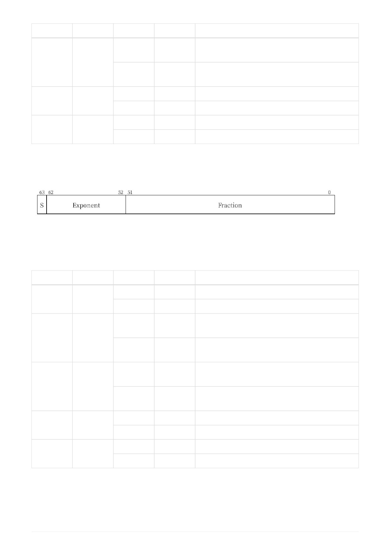
3.1.1.2. Double-precision Floating-point
Figure 4. Double-precision floating-point number format
According to the different values of the fields of S, Exponent and Fraction, the floating-point number
values represented are shown in the table:
Table 5. Double-precision floating-point number calculation method
Exponent
Fraction
S
bit[51]
V
0
0
0
0
+0
1
0
-0
Any value
0
!=0
0
Denormalized number, the value is +2-
1022×(0.Fraction)
Any value
1
Denormalized number, the value is -2-
1022×(0.Fraction)
Any value
Any value
[1,0x7FE]
0
Normalized number, the value is +2Exponent-
1023×(1.Fraction)
Any value
1
Normalized number, the value is -2Exponent-
1023×(1.Fraction)
0x7FF
0
0
0
+∞
1
0
-∞
Any value
Signaling Not a Number, SNaN
0x7FF
!=0
0
Any value
Quiet Not a Number, QNaN
1
For the specific meaning of ±∞, SNaN and QNaN, please refer to the IEEE 754-2008 standard specification.
65
3.1.1.3. Non-numerical Result of Instructions
The non-numerical results produced by floating-point number instructions either come from NaN
propagation or are directly generated. There are two situations where NaN propagation is required.
Case 1: When the instruction generates an Invalid Operation floating-point exception due to a source
operand containing SNaN, but the InvalidOperation floating-point exception enable is invalid, a QNaN result
will be generated at this time. The value of this QNaN is to select the SNaN with the highest priority in the
source operand and propagate it to the corresponding NaN.
The rule for determining the priority of the source operand is: if there are two source operands fj and fk,
then the priority of fj is higher than fk; if there are three source operands fa, fj and fk, then the priority
of fa is higher than fj, fj have higher priority than fk.
The value generation rules for propagation of SNaN to QNaN are as follows:
• If the result is the same length as the source operand, then the highest position of the SNaN mantissa
will be propagated to 1, and the remaining bits remain unchanged. If the result is narrower than the
source operand, then keep the high bits of the mantissa, discard the low bits that exceed the range, and
finally set the highest bit of the mantissa to 1.
•
If the result is wider than the source operand, then the lowest bit of the mantissa will be filled with 0,
and finally the highest position of the mantissa will be 1.
Case 2: When there is no SNaN in the source operand but QNaN exists, the QNaN with the highest priority is
selected as the result of this instruction. At this time, the way of judging the priority of the source operand
is the same as in the above situation.
Except for the above two cases, other cases that need to produce QNaN results will be directly set to the
default QNaN value. The default single-precision QNaN value is 0x7FC00000, and the default double-
precision QNaN value is 0x7FF8000000000000.
3.1.2. Fixed-Point Data Types
Some floating-point instructions (such as floating-point conversion instructions) also manipulate fixed-
point data, including Word (W, length 32b), and Longword (L, length 64b). Both word and longword data
types use two’s complement encoding.
3.1.3. Registers
Floating-point instruction programming involves registers such as Floating-point Register (FR), Condition
Flag Register (CFR) and Floatingpoint Control and Status Register (FCSR).
3.1.3.1. Floating-point Registers
There are 32 FRs, denoted as f0-f31, each of which can be read and written. Only when only floating-point
instructions that manipulate single-precision floating-point numbers and word integers are implemented,
the length of FR is 32 bits. Under normal circumstances, the length of FR is 64 bits, regardless of the LA32
or LA64. There is an “orthogonal” relationship between basic floating-point instructions and floating-point
registers, that is, from an architectural perspective, any floating-point register operand in these instructions
can use any one of the 32 FRs.
66