HUAWEI OptiX OSN 8800 T64/T32 Intelligent Optical Transport Platform. Product Description - part 15
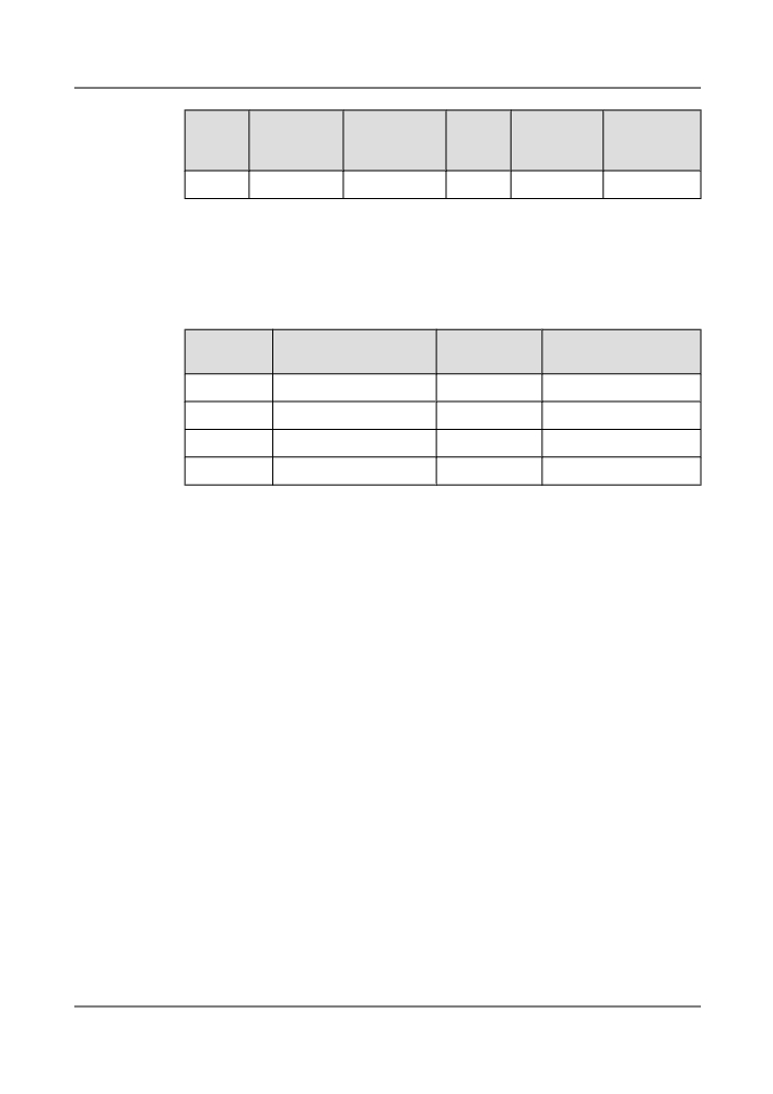
Wavele
Central
Central
Wavele
Central
Central
ngth
Frequency
Wavelength
ngth
Frequency
Wavelength
No.
(THz)
(nm)
No.
(THz)
(nm)
40
194.10
1544.53
80
192.10
1560.61
5.8.3 Nominal Central Wavelengths of the CWDM System
Table 5-17 Nominal central wavelengths of the CWDM system
Wavelengt
Wavelength (nm)
Wavelength
Wavelength (nm)
h No.
No.
11
1471
15
1551
12
1491
16
1571
13
1511
17
1591
14
1531
18
1611
5.8.4 Single-Fiber Bidirectional Transmission
OptiX OSN 8800 CWDM system support single-fiber bidirectional transmission. That is,
bidirectional signals (transmit and receive) of different wavelengths are transported in the same
fiber. As a result, any wavelength(s) among 16 wavelengths in the CWDM band can be added
or dropped. The SBM2 board is applied in the single-fiber bidirectional transmission.
The dispersion supported by the 8-channel CWDM system is 40 km.
5.8.5 Chromatic Dispersion Compensation
The system provides different dispersion compensation solutions to different applications.
For the system that transmits 2.5 Gbit/s, 10 Gbit/s, and 40 Gbit/s signals over G.652, G.653 and
G.655 fibers, the fixed dispersion compensation fibers, such as DCM module and DCU board,
can be used to realize whole spectrum compensation with full dispersion slope match.
For the 40 Gbit/s system, the tunable dispersion compensation module embedded in the receive
unit can control residual dispersion compensation automatically.
5.8.6 SBS Suppresses
The spectral width of signals borne on the laser bias in the OptiX OTN product series is increased
to suppress stimulated Brillouin scattering (SBS).
The 2.5 Gbit/s, 10 Gbit/s, and 40 Gbit/s signals have the same SBS threshold, which is 18 dBm.
The 40 Gbit/s signal is sensitive to nonlinear effects, the maximum launched optical power of
the laser that launches the 40 Gbit/s signal should be limited to 14 dBm. That is:
147

l In the case of the 2.5 Gbit/s and 10 Gbit/s signals, the per-channel maximum launched
optical power is 18 dBm.
l In the case of the 40 Gbit/s signal, the per-channel maximum launched optical power is 14
dBm.
5.8.7 Supervisory Channel
The supervisory information between NEs is transmitted over supervisory channels. Supervisory
channels are as follows:
l Optical supervisory channel (OSC)
l Electric supervisory channel (ESC)
In OSC Mode
In OSC mode, the OSC unit (HSC1/SC1/SC2/ST2) needs to work with the FIU/SFIU board.
The wavelength of the supervisory channel is 1491/1510/1511 nm. The OSC, which adopts the
E1 frame structure, can directly transmit two channels of voice signals at the rate of 64 kbit/s.
The external IP management information can be accessed through the 10 Mbit/s or 100 Mbit/s
Ethernet ports and can be carried by the OSC.
In a ring or mesh network, when a fiber cut occurs in a certain direction of transmission, the
supervision and management information is automatically switched to the supervisory channel
in another direction. Thus the management of the entire network is not affected.
For the details about the OSC, see 5.11.1.1 Optical Supervisory Channel Administration.
In ESC Mode
In ESC mode, the OTU board, tributary board, and line board multiplex the supervisory
information into the service channel for transmission, requiring no optical supervisory channel
units (HSC1/SC1/SC2/ST2). The OTU board, tributary board, and line board realize the ESC
transmission by using the DCC byte or the associated GCC byte compliant with ITU-T G.709.
The external IP supervisory information can be sent to the system through the 10 Mbit/s or 100
Mbit/s Ethernet port and then carried by the ESC.
The ESC reduces the investment of the OSC. It also avoids the insertion loss of the FIU/SFIU.
This lowers the cost and the power budget of optical channels.
The OptiX OSN 8800 realizes the ESC with GCC0 byte or GCC1 and GCC2 bytes. The
bandwidth occupied by GCC bytes varies according to the line rate (OTU rate level). Table
5-18 lists the specific bandwidths occupied by GCC bytes at different OTU rate levels.
Table 5-18 Bandwidth occupied by GCC bytes at different OTU rate levels
OTU Rate Level
GCC Byte
Bandwidth
OTU1
GCC0
192 kbit/s
OTU1
GCC1+GCC2
576 kbit/s
OTU2/OTU2e/
GCC0
192 kbit/s
OTU3
148

OTU Rate Level
GCC Byte
Bandwidth
OTU2/OTU2e/
GCC1+GCC2
1152 kbit/s
OTU3
5.8.8 DRZ Coding Scheme
The differential phase return to zero (DRZ) coding scheme is highly capable of suppressing the
nonlinearity in a 50 GHz channel-spaced 80-channel system.
In the DRZ coding scheme, input differential signals are used to generate positive and negative
return to zero (RZ) coded pulses. These pulses drive the phase regulator to adjust the phase
difference between every two adjacent RZ pulses to 180º before the signals enter the fiber line
for transmission. This effectively reduces the intersymbol interference of DRZ coding to a degree
that parallels the intersymbol interference tolerance of non return to zero (NRZ) coding.
Therefore, the pulse quality is ensured even in the case of large accumulated dispersion, and the
signals are effectively prevented from distortion caused by dispersion.
The chirping feature is introduced to the DRZ coding scheme. Therefore, the DRZ-coded signals
are highly tolerant of nonlinear effects such as SBS, FWM, SPM, and SRS in the fiber.
5.8.9 ODB Technology
The OTU adopting the optical duobinary (ODB) coding has a narrow optical spectrum, and it
can be used in the system with 50 GHz channel spacing.
The input signals are provided with pre-coding, and the three status code (-1, 0, 1) sequence is
output. The code sequence drive modulator is used to convert electrical signals to optical signals.
On the receive side, a common light intensity detector is used to receive the signals.
The 3 dB bandwidth of ODB is about 25% of the 3 dB bandwidth of NRZ. The spectral efficiency
of ODB is higher than that of NRZ. Therefore, it is suitable for WDM transmission with high
density.
5.8.10 DQPSK Technology
DQPSK is used to transport 40 Gbit/s signal.
DQPSK is a new modulation format. On the transmit side, the input electrical signals are
differentially encoded. Then, the modulator performs quadrature phase shift keying modulation
and outputs the optical signals in four phases: 0, π/2, π, and 3π/2. On the receive side, the modem
differentially decodes the optical signals; the signals are received in an equalized manner. The
receiver sensitivity of the DQPSK modulation format is 3 dB higher than that of the amplitude
modulation format.
DQPSK is a multilevel modulation format in which the bit rate is two times of the baud rate.
Hence, DQPSK is highly suitable for the 40G high-speed transmission system. In the DQPSK
modulation format, the spectrum width is narrow and the output spectrum is smooth. As a result,
the DQPSK modulation format can effectively suppress various nonlinear effects of the fiber.
The phase shift helps reduce the phase-related nonlinear effects (such as SPM, XPM, and FWM)
and enhance the tolerance to chromatic dispersion and polarization mode dispersion. Hence,
149
DQPSK is a critical modulation format used in the long-haul, high-speed, and large-capacity
optical transmission.
Enhanced DQPSK further elevates the nonlinearity tolerance of the system, and is currently the
best coding technology for 40G ultra long haul transmission.
5.8.11 Tunable Wavelengths
The OptiX OSN 8800 supports tunable wavelengths. It adopts 40 Gbit/s, 10 Gbit/s and 2.5 Gbit/
s OTUs that support tunable wavelengths.
l The 40 Gbit/s and 10 Gbit/s OTUs support tunable wavelengths in up to 80 channels with
50 GHz spacing in C band.
l The 2.5 Gbit/s OTUs support tunable wavelengths in up to 40 channels with 100 GHz
spacing in C band.
In addition, the tunable wavelength OTUs can also function as spare parts to substitute OTUs
of different wavelengths. This reduces the number of OTUs and lowers the cost. When the
wavelength-tunable OTUs work with dynamic optical add/drop multiplexing units, the dynamic
wavelength grooming is realized.
5.8.12 EDFA Technology
The OptiX OTN product series use advanced Erbium-Doped Fibre Amplifier (EDFA)
technology, with varying optical power output and gain to suit different applications related to
long haul transmission, reducing the need for regeneration.
EDFA adopts gain locking technology and transient control technology to make the gain of each
channel independent of the number of channels. Adding or dropping channels does not cause
burst bit error in the existing channels.
The optical amplifiers adopted by the system are capable of amplifying the signals that are spaced
at 100 GHz and 50 GHz in the C band and comply with ITU-T G.694.1.
5.8.13 Raman Amplification
The combination of Raman amplifier and Erbium-doped fiber amplifier (EDFA) realizes
wideband flat gain. The interference of system noise and non-linear effect on the system is
effectively decreased and the transmission distance is increased.
Raman amplifier works 20 to 30 km away from Raman pump laser. If there is optical power loss
higher than 7 dB within a 20-kilometer distance from Raman pump laser, the optical power gain
realized by Raman amplifier decreases and Raman amplifier cannot work normally. If there is
optical power loss higher than 7 dB beyond a 30-kilometer distance from Raman pump laser,
the optical power gain realized by Raman amplifier remains unaffected.
The LSH/APC (E2000/APC) connectors for the RAMAN amplifier are recommended.
5.8.14 Jitter Suppression Function
With a jitter suppression unit between the optical receive module and the optical transmit module,
the OptiX OSN 8800 has excellent jitter suppression function.
5.8.15 Automatic Laser Shutdown
150
The OTU board and tributary board provide the automatic laser shutdown (ALS) function.
With the ALS function, the OTU board and tributary board can automatically shut down or turn
on the laser based on the condition of the input optical signals to prevent personal injury.
The ALS function applies to the client side of the OTU board and tributary board. This function
can be enabled or disabled through the network management system. The configuration of
optical interface is shown in Figure 5-41 (a).
NOTE
The WDM-side optical interface of the LWXS also supports the ALS function.
The ALS function is realized through the following way:
l When no optical signals are input to the receive optical interface on the client side of the
opposite OTU board, the local OTU board automatically shuts down the laser for the output
optical interface on the corresponding client side, as shown in the Figure 5-41 (b).
l When no optical signals are input to the receive optical interface on the WDM side of the
OTU board, the OTU board automatically shuts down all the lasers for the output optical
interface on the client side with the ALS function enabled, as shown in Figure 5-41 (c).
NOTE
Figure 5-41 shows the ALS function realization of the OTU board with service convergence function. The
ALS function of the OTU board without service convergence function is realized in the same way.
NOTE
The ALS and LPT functions of a board cannot be enabled at the same time.
151
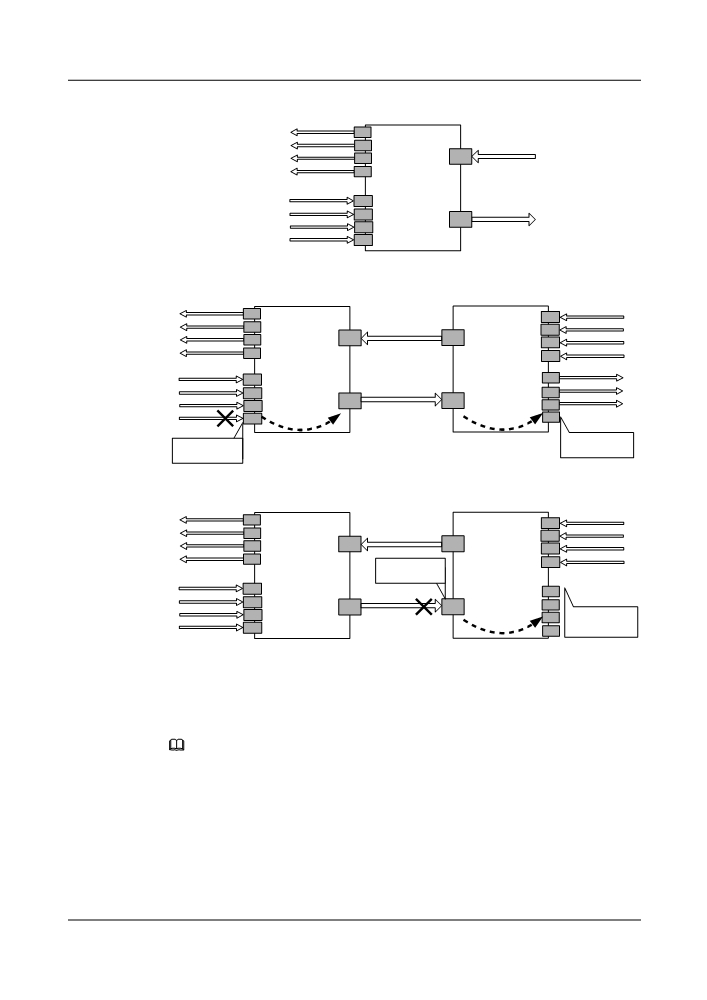
Figure 5-41 ALS function diagram
Tx
Tx
ALS
enabled
Tx
IN
Tx
OTU
Rx
ALSenabled
Rx
OUT
Rx
Rx
client side
WDM side
(a)Configuration of optical interfaces
Tx
Rx
Tx
Rx
ALS
enabled
Tx
IN
OUT
Rx
Tx
Rx
OTU
OTU
Rx
Tx
Rx
Tx
OUT
IN
ALSenabled
Rx
Tx
Rx
Tx
client side
WDM side
WDM side
client side
Automatic laser
No input optical
shutdown
signals
(b) No signals received on the
client side of the far end
Tx
Rx
Tx
ALS
enabled
Rx
Tx
IN
OUT
Rx
Tx
Rx
No input optical
OTU
signals
OTU
Rx
Tx
Rx
OUT
IN
ALS
enabled
Tx
Rx
Tx
Automatic laser
Rx
shutdown
Tx
client side
WDM side
WDM side
client side
(c) No signals received
on the WDM side
NOTE
The ALS function provided by the OptiX WDM products does not refer to the ALS mentioned in ITU-T
G.664, only that the acronyms of the two are the same.
The ALS function does not support the scenario of service broadcasting.
5.9 Clock Synchronization Solutions
This section describes the clock synchronization solutions used by the OptiX OSN 8800in
different scenarios.
152
5.9.1 Clock Network Models
This section describes a typical clock network model used by an OTN network.
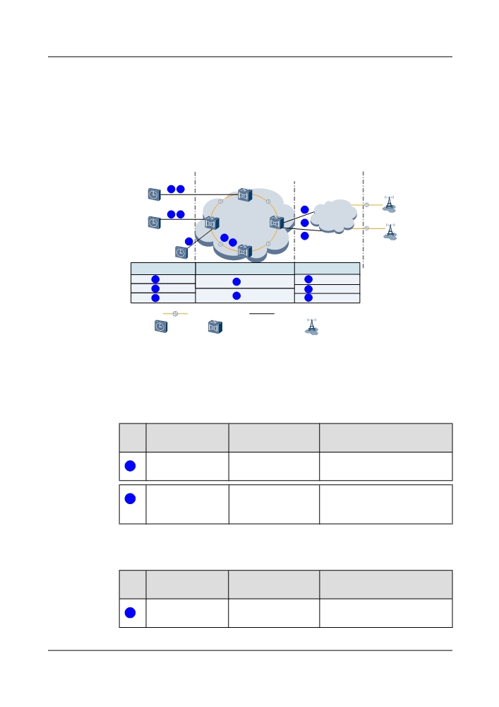
As shown in Figure 5-42, a complete clock synchronous network consists of frequency/phase
sources, a transport network, and base stations.
Figure 5-42 Typical clock network model
Frequency/Phase Sources
Transport Network
Base Stations
1
2
Slave
BITS
A
6
1 2
Node B
Master
Client Network
B
OTN Network
D
7
BITS
8
4
C
3
5
Node B
G
Input of clock signals
Transmission Method
Output of clock signals
1
2M
6
2M
4 OSC
2
1PPS+TOD
7
1PPS+TOD
5
ESC
3 GE
8
GE/10GE
Optical Cables
Cables
BITS
OptiX OTN product series
Node B
Input of clock signals
Table 5-19 Physical clock synchronization
Mar
Frequency source
Board
Description
k
2M external clock
TN52STG,
This method is recommended.
1
signals
TNK2STG, TN52STI
GE clock signals
TN52TOG,
The OptiX OSN 8800 supports
3
over service
TN11LEM24,
through the GE ports to implement
TN54THA, TN54TOA
frequency synchronization.
Table 5-20 IEEE 1588v2 synchronization
Mar
Phase source
Board
Description
k
1PPS+TOD time
TN52STG,
This method is recommended.
2
signals
TNK2STG, TN52STI
153
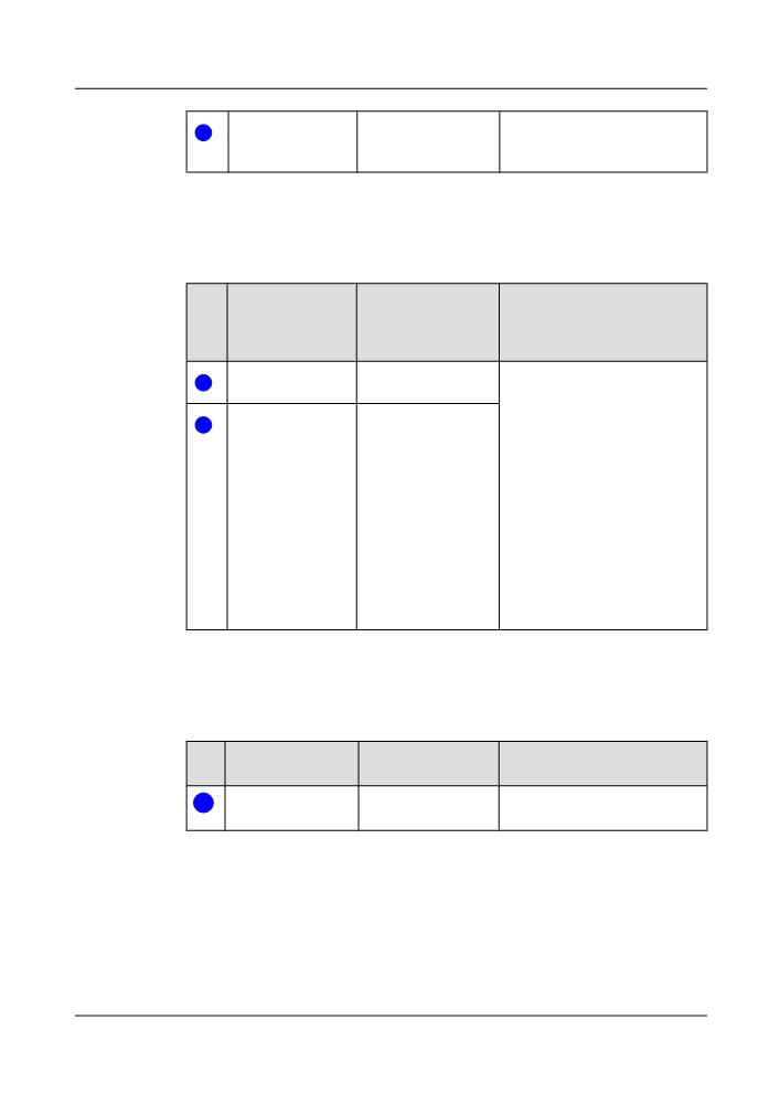
GE clock signals
TN52TOG,
The OptiX OSN 8800 supports
3
over service
TN54THA, TN54TOA
through the GE ports to implement
phase synchronization.
Transmission of clock signals over the OTN network
Table 5-21 Physical clock synchronization or IEEE 1588v2 synchronization
Mar
Clock
Board
k
Synchronization
Description
Implementation
Method
OSC channels
TN11ST2
4
ESC channels
TN52ND2, TN54NQ2,
5
TN54NPO2,
TN55NPO2,
TN54NS3,
The OptiX OSN 8800 supports
TN55NPO2E,
receive frequency signals using an
TN53NQ2, TN53ND2,
ESC or OSC channel.
TN53NS2, TN55TQX,
TN53TDX,
TN54THA,
TN54TOA,
TN52TOG,
TN11LEM24,
TN11LEX4
Output of clock signals
Table 5-22 Physical clock synchronization
Ma
Frequency source
Board
Description
rk
2M external clocks
TN52STG,
This method is recommended.
6
TNK2STG, TN52STI
154
Ma
Frequency source
Board
Description
rk
GE or 10GE clock
l GE: TN52TOG,
The OptiX OSN 8800 supports
8
signals over services
TN11LEM24,
through the GE or 10GE ports to
TN54THA,
implement frequency
TN54TOA
synchronization.
l 10GE:
TN11LEM24,
TN11LEX4,
TN55TQX,
TN53TDX
Table 5-23 IEEE 1588v2 synchronization
Ma
Phase source
Board
Description
rk
1PPS+TOD time
TN52STG,
This method is recommended.
7
signals
TNK2STG, TN52STI
GE or 10GE clock
l GE: TN52TOG,
The OptiX OSN 8800 supports
8
signals over services
TN54THA,
through the GE or 10GE ports to
TN54TOA
implement phase synchronization.
l 10GE: TN55TQX,
TN53TDX
NOTE
Figure 5-42 shows that various methods can be used to transmit clock signals over an OTN network. In
practical application, however, it is recommended that only one method be used to transmit clock signals
over the same OTN network.
5.9.2 Methods and Typical Applications of Frequency
Synchronization
This section describes the implementation methods and the typical applications of frequency
synchronization.
Methods of Obtaining Frequency Sources
Frequency sources can be obtained by:
l Acquiring 2M external clock signals
l Acquiring clock signals over GE/10GE services
For details about the methods of obtaining a frequency source, see Methods of Obtaining Clock
Sources.
155
NOTE
When an OptiX OSN 8800 is used to obtain 2M external clocks from a BITS or OptiX PTN and other
device, the cable connecting them must be shorter than 200 m.
Frequency Synchronization Implementation Methods
Two methods are available for implementing frequency synchronization.
l Frequency synchronization is implemented based on physical clocks, which are extracted
from line data streams.
Physical clock synchronization does not consume service bandwidth and is independent of
packet delay variation (PDV). However, physical clock synchronization can be
implemented only when equipment supports physical clocks. Therefore, every node on the
network must support physical clocks for this method to be used networkwide. For more
information, see Introduction.
l Frequency synchronization is implemented based on the received and transmitted
timestamps in Sync messages defined by the IEEE 1588v2 protocol.
IEEE 1588v2-compliant frequency synchronization involves two actions: frequency
gauging and frequency correction. This method provides a synchronization precision close
to that of frequency synchronization based on physical clocks. For more information, see
IEEE 1588v2-Compliant Frequency Synchronization.
NOTE
An OptiX OSN 8800 supports the following methods for frequency synchronization: IEEE 1588v2 and
physical layer clock synchronization. Synchronous Ethernet is one approach to physical layer clock
synchronization. At one time, the OptiX OTN product series can use either IEEE 1588v2 or synchronous
Ethernet for frequency synchronization. It is recommended that only one method be used to transmit clock
signals over the same OTN network.
Typical Application of Frequency Synchronization
Physical clock synchronization is used as an example to describe two application scenarios
corresponding to the two methods of obtaining frequency sources from a BITS. Figure 5-43
shows the application where frequency sources are obtained from clock signals carried over GE
services, and Figure 5-44 shows the application where frequency sources are obtained from 2M
external clocks.
Application 1: Clock transmission based on physical clocks carried over GE services
As shown in Figure 5-43, the other device (such as the OptiX PTN device) obtains clock signals
from the BITS device and transmits the clock signals to the connected OptiX OSN 8800 on the
OTN network. On the other side of the OTN network, another OptiX OSN 8800 transmits the
clock signals to the two other devices (such as OptiX PTN devices or OptiX OSN 1800) over
GE services. After receiving the clock signals, the two other devices (such as OptiX PTN devices
or OptiX OSN 1800) transmit them to the Node Bs. For details about the configurations, see
Example Description.
156
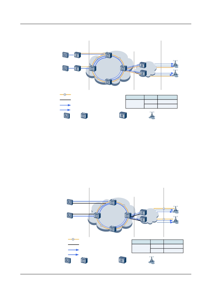
Figure 5-43 Clock transmission based on physical clocks carried over GE services (using ESC
channels over the OTN network)
Frequency/Phase Sources
Transport Network
Base Stations
GE
East
West
Slave
BITS
H
West
A
East
GE
GE
F
Master
B
D
BITS
OTN Network
E
West
G
East
C
West
East
Optical Cables
Sites
Direction
Board
Cables
East
12-52ND2-1
A,B,C,D
Physical synchronization route
West
12-52ND2-2
Physical synchronization protection route
BITS
OptiX OTN product series
Other devices
Node B
Application 2: Clock transmission based on physical clocks from 2M external clocks
As shown in Figure 5-44, on one side of the OTN network, two OptiX OSN 8800 obtain 2M
clock signals from the master and slave BITS devices and transmit them to other OptiX OSN
8800 on the network. On the other side of the network, after processing the clock signals by
using the OSC boards, the egress OptiX OSN 8800 transmits them to the connected other devices
(such as OptiX PTN devices or OptiX OSN 1800). Then, the other devices (such as OptiX PTN
devices or OptiX OSN 1800) transmit the clock signals to the Node Bs. For details about the
configurations, see Example Description.
Figure 5-44 Clock transmission based on physical clocks from 2M external clocks (using OSC
channels over the OTN network)
Frequency/Phase Sources
Transport Network
Base Stations
2M Clock
East
West
Slave
BITS
A
GE
2M Clock
West
East
OTN
E
Master
B
Network
D
BITS
F
East
West
C
West
East
Optical Cables
Sites
Direction
Board
Cables
East
1-11ST2-1
A,B,C,D
Physical synchronization route
West
1-11ST2-2
Physical synchronization protection route
BITS
OptiX OTN product series
Other devices
Node B
157