Intel 64 and IA-32 Architectures. Software Developer’s Manual (2026) - page 69
ENCLAVE CODE DEBUG AND PROFILING
EENTER
Inst1
BR2
Inst3
Inst4
Fault
Inst4
AEP
AEP
OS
IRET
AEP
ERESUME
Inst4
BR5
Inst6
EEXIT
Inst7
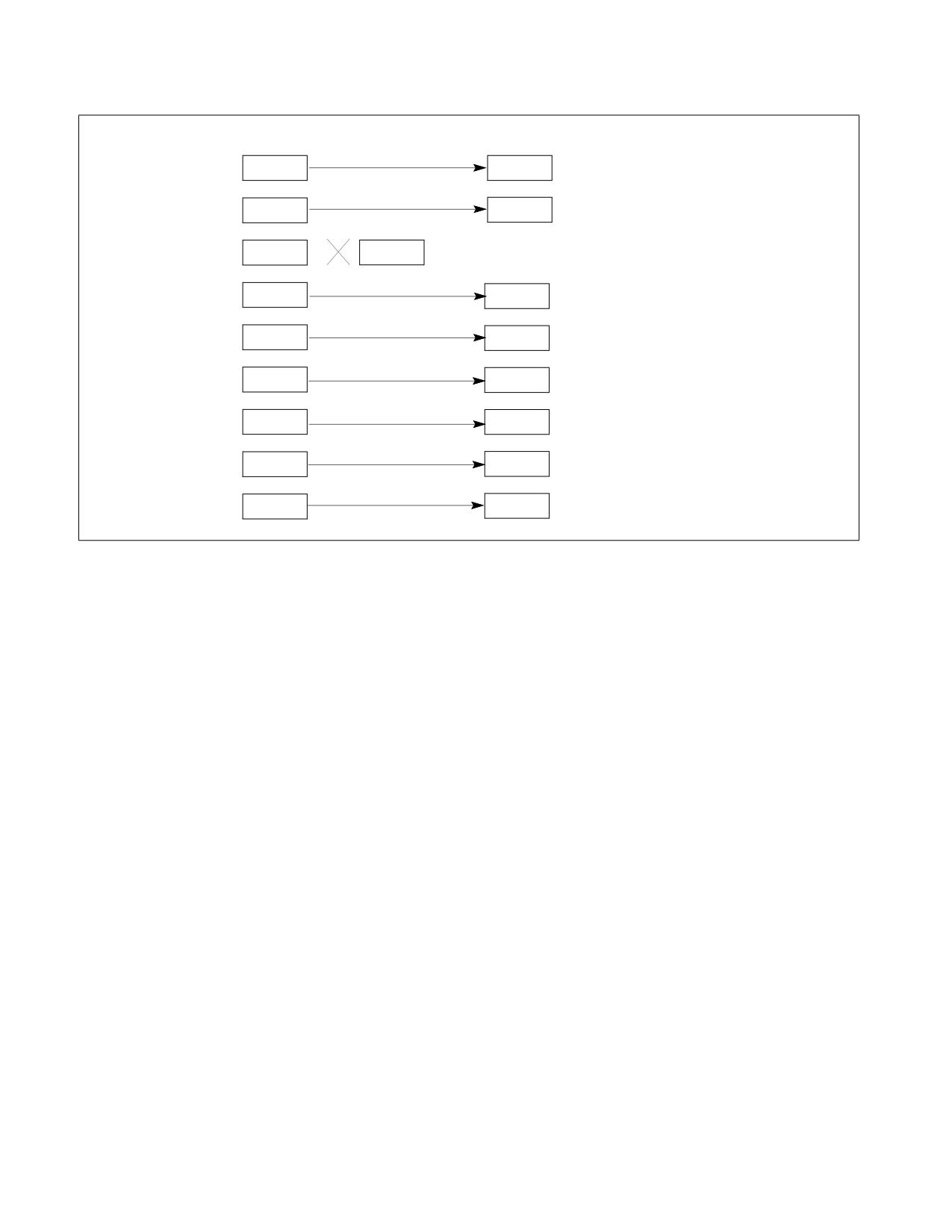
Figure 43-3. LBR Stack Interaction with Opt-in Entry
43.5.2.2 LBR Stack on Opt-out Entry
An opt-out entry into an enclave suppresses last branch recording facilities, and enclave exit after an opt-out entry
un-suppresses last branch recording facilities.
Opt-out entry into an enclave does not push any record on LBR stack.
If last branch recording facilities were enabled at the time of enclave entry, then EEXIT following such an enclave
entry pushes one record on LBR stack. The MSR_LASTBRANCH_n_FROM_IP of such record holds the linear address
of the instruction (EENTER or ERESUME) that was used to enter the enclave, while the MSR_LAST-
BRANCH_n_TO_IP of such record holds linear address of the destination of EEXIT.
Additionally, if last branch recording facilities were enabled at the time of enclave entry, then an AEX after such an
entry pushes one record on LBR stack, before pushing record for the event causing the AEX if the event pushes a
record on LBR stack. The MSR_LASTBRANCH_n_FROM_IP of the new record holds linear address of the instruction
(EENTER or ERESUME) that was used to enter the enclave, while MSR_LASTBRANCH_n_TO_IP of the new record
holds linear address of the AEP. If the event causing AEX pushes a record on LBR stack, then the MSR_LAST-
BRANCH_n_FROM_IP for that record holds linear address of the AEP.
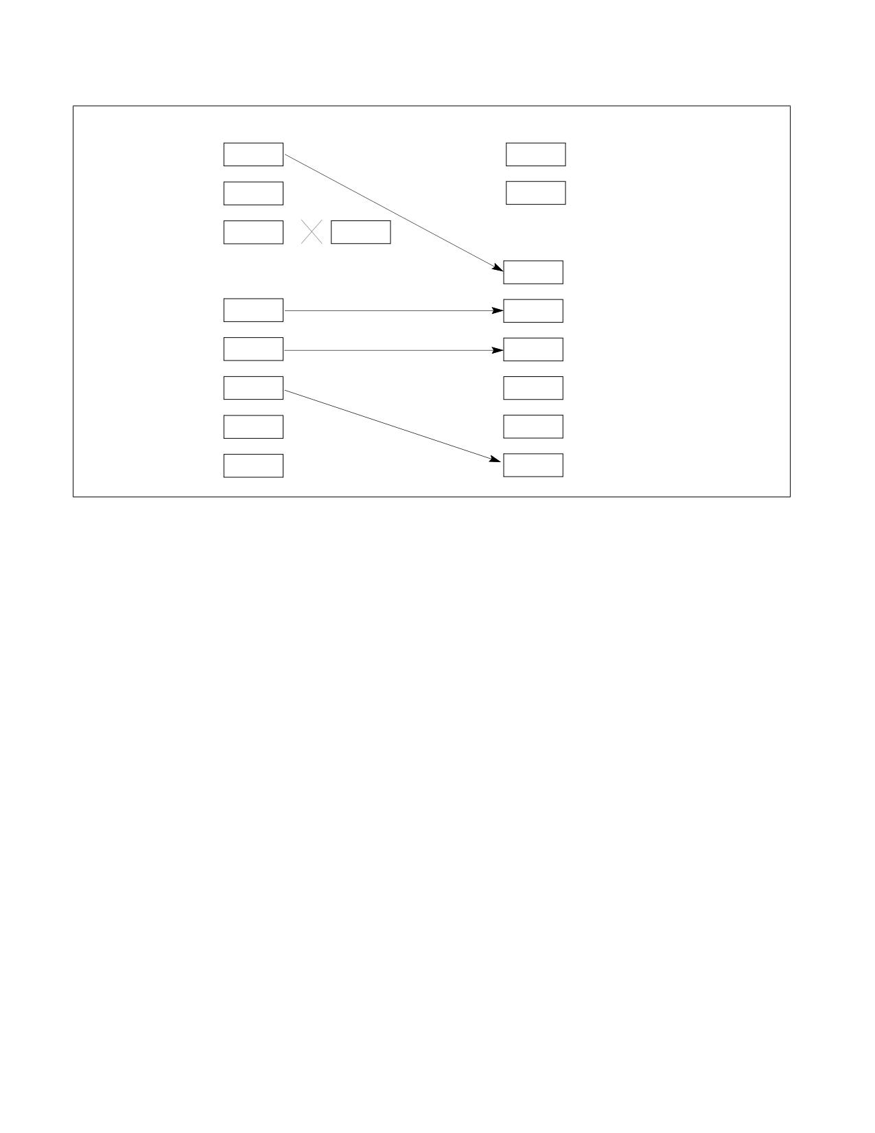
Figure 43-4 shows an example of LBR stack manipulation after an opt-out entry. Every arrow in this picture indi-
cates a branch record pushed on the LBR stack. The “From IP” of the branch record contains the linear address of
the instruction located at the start of the arrow, while the “To IP” of the branch record contains the linear address
of the instruction at the end of the arrow.
43-6
Vol. 3D
ENCLAVE CODE DEBUG AND PROFILING
EENTER
Inst1
BR2
Inst3
Inst4
Fault
AEP
AEP
OS
IRET
AEP
ERESUME
Inst4
BR5
Inst6
EEXIT
Inst7
Figure 43-4. LBR Stack Interaction with Opt-out Entry
43.5.2.3 Mispredict Bit, Record Type, and Filtering
All branch records resulting from Intel SGX instructions/AEXs are reported as predicted branches, and conse-
quently, bit 63 of MSR_LASTBRANCH_n_FROM_IP for such records is set. Branch records due to these Intel SGX
operations are always non-HLE/non-RTM records.
EENTER, ERESUME, EEXIT, and AEX are considered to be far branches. Consequently, bit 8 in MSR_LBR_SELECT
controls filtering of the new records introduced by Intel SGX.
43.6
INTERACTION WITH PERFORMANCE MONITORING
43.6.1 IA32_PERF_GLOBAL_STATUS Enhancement
On processors supporting Intel SGX, the IA32_PERF_GLOBAL_STATUS MSR provides a bit indicator, known as “Anti
Side-channel Interference” (ASCI) at bit position 60. If this bit is 0, the performance monitoring data in various
performance monitoring counters are accumulated normally as defined by relevant architectural/microarchitec-
tural conditions. If the ASCI bit is set, the contents in various performance monitoring counters can be affected by
the direct or indirect consequence of Intel SGX protection of enclave code executing in the processor.
43.6.2 Performance Monitoring with Opt-in Entry
An opt-in enclave entry allow performance monitoring logic to observe the contribution of enclave code executing
in the processor. Thus the contents of performance monitoring counters does not distinguish between contribution
originating from enclave code or otherwise. All counters, events, precise events, etc. continue to work as defined
in the IA32/Intel 64 Software Developer Manual. Consequently, bit 60 of IA32_PERF_GLOBAL_STATUS MSR is not
set.
Vol. 3D
43-7
ENCLAVE CODE DEBUG AND PROFILING
43.6.3 Performance Monitoring with Opt-out Entry
In general, performance monitoring activities are suppressed when entering an opt-out enclave. This applies to all
thread-specific, configured performance monitoring, except for the cycle-counting fixed counter, IA32_-
FIXED_CTR1 and IA32_FIXED_CTR2. Upon entering an opt-out enclave, IA32_FIXED_CTR0, IA32_PMCx will stop
accumulating counts. Additionally, if PEBS is configured to capture PEBS record for this thread, PEBS record gener-
ation will also be suppressed. Consequently, bit 60 of IA32_PERF_GLOBAL_STATUS MSR is set.
Performance monitoring on the sibling thread may also be affected. Any one of IA32_FIXED_CTRx or IA32_PMCx
on the sibling thread configured to monitor thread-specific eventing logic with AnyThread =1 is demoted to count
only MyThread while an opt-out enclave is executing on the other thread.
43.6.4 Enclave Exit and Performance Monitoring
When a logical processor exits an enclave, either via ENCLU[EEXIT] or via AEX, all performance monitoring activity
(including PEBS) on that logical processor that was suppressed is unsuppressed.
Any counters that were demoted from AnyThread to MyThread on the sibling thread are promoted back to
AnyThread.
43.6.5 PEBS Record Generation on Intel® SGX Instructions
All leaf functions of the ENCLS instruction report “Eventing RIP” of the ENCLS instruction if a PEBS record is gener-
ated at the end of the instruction execution. Additionally, the EGETKEY and EREPORT leaf functions of the ENCLU
instruction report “Eventing RIP” of the ENCLU instruction if a PEBS record is generated at the end of the instruction
execution.
If the EENTER and ERESUME leaf functions are performing an opt-in entry report “Eventing RIP” of the ENCLU
instruction if a PEBS record is generated at the end of the instruction execution. On the other hand, if these leaf
functions are performing an opt-out entry, then these leaf functions result in PEBS being suppressed, and no PEBS
record is generated at the end of these instructions.
A PEBS record is generated if there is a PEBS event pending at the end of EEXIT (due to a counter overflowing
during enclave execution or during EEXIT execution). This PEBS record contains the architectural state of the
logical processor at the end of EEXIT. If the enclave was entered via an opt-in entry, then this record reports the
“Eventing RIP” as the linear address of the ENCLU[EEXIT] instruction. If the enclave was entered via an opt-out
entry, then the record reports the “Eventing RIP” as the linear address of the ENCLU[EENTER/ERESUME] instruc-
tion that performed the last enclave entry.
A PEBS record is generated after the AEX if there is a PEBS event pending at the end of AEX (due to a counter over-
flowing during enclave execution or during AEX execution). This PEBS record contains the synthetic state of the
logical processor that is established at the end of AEX. For opt-in entry, this record has the EVENTING_RIP set to
the RIP saved in the SSA. For opt-out entry, the record has the EVENTING_RIP set to the linear address of
EENTER/ERESUME used for the last enclave entry.
If the enclave was entered via an opt-in entry, then this record reports the “Eventing RIP” as the linear address in
the SSA of the enclave (a.k.a., the “Eventing LIP” inside the enclave). If the enclave was entered via an opt-out
entry, then the record reports the “Eventing RIP” as the linear address of the ENCLU[EENTER/ERESUME] instruc-
tion that performed the last enclave entry.
A second PEBS event may be pended during the Enclave Exiting Event (EEE). If the PEBS event is taken at the end
of delivery of the EEE then the “Eventing RIP” in this second PEBS record is the linear address of the AEP.
43.6.6 Exception-Handling on PEBS/BTS Loads/Stores after AEX
As noted in Section 20.4.9.2, recording in the BTS buffer or in the PEBS buffer may not operate properly if accesses
to any of the DS save area sections cause page faults or VM exits. Such page faults or VM exits, if they occur, are
delivered immediately to the OS or VMM, and generation of a BTS or PEBS record is skipped and may leave the
buffers in a state where they have a partial BTS or PEBS records.
However, any events that are detected during PEBS/BTS record generation at the end of AEX and before delivering
the Enclave Exiting Event (EEE) cannot be reported immediately to the OS/VMM, as an event window is not open at
43-8
Vol. 3D
ENCLAVE CODE DEBUG AND PROFILING
the end of AEX. Consequently, fault-like events such as page faults, EPT faults, EPT mis-configuration, and
accesses to APIC-access page detected on stores to the PEBS/BTS buffer are not reported, and generation of the
PEBS and/or BTS record at the end of AEX is aborted (this may leave the buffers in a state where they have partial
PEBS or BTS records). Trap-like events detected on stores to the PEBS/BTS buffer (such as debug traps) are
pended until the next instruction boundary, where they are handled according to the architecturally defined
priority. The processor continues the handling of the Enclave Exiting Event (SMI, NMI, interrupt, exception delivery,
VM exit, etc.) after aborting the PEBS/BTS record generation.
43.6.6.1 Other Interactions with Performance Monitoring
For opt-in entry, EENTER, ERESUME, EEXIT, and AEX are all treated as predicted far branches, and any counters
that are counting such branches are incremented by 1 as a part of retirement of these instructions. Retirement of
these instructions is also counted in any counters configured to count instructions retired.
For opt-out entry, execution inside an enclave is treated as a single predicted branch, and all branch-counting
performance monitoring counters are incremented accordingly. Additionally, such execution is also counted as a
single instruction, and all performance monitoring counters counting instructions are incremented accordingly.
Enclave entry does not affect any performance monitoring counters shared between cores.
Vol. 3D
43-9
ENCLAVE CODE DEBUG AND PROFILING
43-10
Vol. 3D

APPENDIX A
VMX CAPABILITY REPORTING FACILITY
The ability of a processor to support VMX operation and related instructions is indicated by
CPUID.01H:ECX.VMX[5] = 1. A value 1 in this bit indicates support for VMX features.
Support for specific features detailed in Chapter 29 and other VMX chapters is determined by reading values from
a set of capability MSRs. These MSRs are indexed starting at MSR address 480H. VMX capability MSRs are read-
only; an attempt to write them (with WRMSR) produces a general-protection exception (#GP(0)). They do not exist
on processors that do not support VMX operation; an attempt to read them (with RDMSR) on such processors
produces a general-protection exception (#GP(0)).
A.1
BASIC VMX INFORMATION
The IA32_VMX_BASIC MSR (index 480H) consists of the following fields:
• Bits 30:0 contain the 31-bit VMCS revision identifier used by the processor. Processors that use the same VMCS
revision identifier use the same size for VMCS regions (see subsequent item on bits 44:32).1
• Bit 31 is always 0.
• Bits 44:32 report the number of bytes that software should allocate for the VMXON region and any VMCS
region. It is a value greater than 0 and at most 4096 (bit 44 is set if and only if bits 43:32 are clear).
• Bit 48 indicates the width of the physical addresses that may be used for the VMXON region, each VMCS, and
data structures referenced by pointers in a VMCS (I/O bitmaps, virtual-APIC page, MSR areas for VMX transi-
tions). If the bit is 0, these addresses are limited to the processor’s physical-address width.2 If the bit is 1,
these addresses are limited to 32 bits. This bit is always 0 for processors that support Intel 64 architecture.
• If bit 49 is read as 1, the logical processor supports the dual-monitor treatment of system-management
interrupts and system-management mode. See Section 34.15 for details of this treatment.
• Bits 53:50 report the memory type that should be used for the VMCS, for data structures referenced by
pointers in the VMCS (I/O bitmaps, virtual-APIC page, MSR areas for VMX transitions), and for the MSEG
header. If software needs to access these data structures (e.g., to modify the contents of the MSR bitmaps), it
can configure the paging structures to map them into the linear-address space. If it does so, it should establish
mappings that use the memory type reported bits 53:50 in this MSR.3
As of this writing, all processors that support VMX operation indicate the write-back type. The values used are
given in Table A-1.
Table A-1. Memory Types Recommended for VMCS and Related Data Structures
Value(s)
Field
0
Uncacheable (UC)
1-5
Not used
6
Write Back (WB)
7-15
Not used
1. Earlier versions of this manual specified that the VMCS revision identifier was a 32-bit field in bits 31:0 of this MSR. For all proces-
sors produced prior to this change, bit 31 of this MSR was read as 0.
2. On processors that support Intel 64 architecture, the pointer must not set bits beyond the processor's physical address width. This
width is denoted MAXPHYADDR and is derived from the value enumerated in CPUID.80000008H:EAX[7:0]. If
IA32_TME_ACTIVATE[0] = 1 (indicating that TME has been configured), MAXPHYADDR is reduced by the value of IA32_TME_ACTI-
VATE[39:36] when a logical processor is outside secure arbitration mode (SEAM; see Chapter 35); the value is not reduced in SEAM.
3. Alternatively, software may map any of these regions or structures with the UC memory type. (This may be necessary for the MSEG
header.) Doing so is discouraged unless necessary as it will cause the performance of software accesses to those structures to suf-
fer.
Vol. 3D A-1
VMX CAPABILITY REPORTING FACILITY
• If bit 54 is read as 1, the processor reports information in the VM-exit instruction-information field on VM exits
due to execution of the INS and OUTS instructions (see Section 30.2.5). This reporting is done only if this bit is
read as 1.
• Bit 55 is read as 1 if any VMX controls that default to 1 may be cleared to 0. See Appendix A.2 for details. It also
reports support for the VMX capability MSRs IA32_VMX_TRUE_PINBASED_CTLS, IA32_VMX_TRUE_PROC-
BASED_CTLS, IA32_VMX_TRUE_EXIT_CTLS, and IA32_VMX_TRUE_ENTRY_CTLS. See Appendix A.3.1,
Appendix A.3.2, Appendix A.4, and Appendix A.5 for details.
• If bit 56 is read as 1, software can use VM entry to deliver a hardware exception with or without an error code,
regardless of vector (see Section 29.2.1.3).
• If bit 58 is read as 1, the processor provides VMX nested-exception support. With this support, software may
indicate that an injected event is a nested exception (see Section 29.2.1.3 and Section 29.6.1.1), and the
VM exits will indicate whether an event is an exception encountered during FRED event delivery (see Section
30.2.2 and Section 30.2.4). Any processor that supports FRED transitions will provide VMX nested-exception
support.
• The values of bits 47:45, bit 57, and bits 63:59 are reserved and are read as 0.
A.2
RESERVED CONTROLS AND DEFAULT SETTINGS
As noted in Chapter 29, “VM Entries‚” certain VMX controls are reserved and must be set to a specific value (0 or 1)
determined by the processor. The specific value to which a reserved control must be set is its default setting.
Software can discover the default setting of a reserved control by consulting the appropriate VMX capability MSR
(see Appendix A.3 through Appendix A.5).
Future processors may define new functionality for one or more reserved controls. Such processors would allow
each newly defined control to be set either to 0 or to 1. Software that does not desire a control’s new functionality
should set the control to its default setting. For that reason, it is useful for software to know the default settings of
the reserved controls.
Default settings partition the various controls into the following classes:
• Always-flexible. These have never been reserved.
• Default0. These are (or have been) reserved with a default setting of 0.
• Default1. They are (or have been) reserved with a default setting of 1.
As noted in Appendix A.1, a logical processor uses bit 55 of the IA32_VMX_BASIC MSR to indicate whether any of
the default1 controls may be 0:
• If bit 55 of the IA32_VMX_BASIC MSR is read as 0, all the default1 controls are reserved and must be 1.
VM entry will fail if any of these controls are 0 (see Section 29.2.1).
• If bit 55 of the IA32_VMX_BASIC MSR is read as 1, not all the default1 controls are reserved, and some (but
not necessarily all) may be 0. The CPU supports four (4) new VMX capability MSRs: IA32_VMX_TRUE_PIN-
BASED_CTLS, IA32_VMX_TRUE_PROCBASED_CTLS, IA32_VMX_TRUE_EXIT_CTLS, and IA32_VMX_TRUE_EN-
TRY_CTLS. See Appendix A.3 through Appendix A.5 for details. (These MSRs are not supported if bit 55 of the
IA32_VMX_BASIC MSR is read as 0.)
A.3
VM-EXECUTION CONTROLS
There are separate capability MSRs for the pin-based VM-execution controls, the primary processor-based VM-
execution controls, the secondary processor-based VM-execution controls, and the tertiary processor-based VM-
execution controls. These are described in Appendix A.3.1, Appendix A.3.2, Appendix A.3.3, and Appendix A.3.4,
respectively.
A-2
Vol. 3D
VMX CAPABILITY REPORTING FACILITY
A.3.1
Pin-Based VM-Execution Controls
The IA32_VMX_PINBASED_CTLS MSR (index 481H) reports on the allowed settings of most of the pin-based
VM-execution controls (see Section 27.6.1):
• Bits 31:0 indicate the allowed 0-settings of these controls. VM entry allows control X (bit X of the pin-based
VM-execution controls) to be 0 if bit X in the MSR is cleared to 0; if bit X in the MSR is set to 1, VM entry fails if
control X is 0.
Exceptions are made for the pin-based VM-execution controls in the default1 class (see Appendix A.2). These
are bits 1, 2, and 4; the corresponding bits of the IA32_VMX_PINBASED_CTLS MSR are always read as 1. The
treatment of these controls by VM entry is determined by bit 55 in the IA32_VMX_BASIC MSR:
- If bit 55 in the IA32_VMX_BASIC MSR is read as 0, VM entry fails if any pin-based VM-execution control in
the default1 class is 0.
- If bit 55 in the IA32_VMX_BASIC MSR is read as 1, the IA32_VMX_TRUE_PINBASED_CTLS MSR (see
below) reports which of the pin-based VM-execution controls in the default1 class can be 0 on VM entry.
• Bits 63:32 indicate the allowed 1-settings of these controls. VM entry allows control X to be 1 if bit 32+X in
the MSR is set to 1; if bit 32+X in the MSR is cleared to 0, VM entry fails if control X is 1.
If bit 55 in the IA32_VMX_BASIC MSR is read as 1, the IA32_VMX_TRUE_PINBASED_CTLS MSR (index 48DH)
reports on the allowed settings of all of the pin-based VM-execution controls:
• Bits 31:0 indicate the allowed 0-settings of these controls. VM entry allows control X to be 0 if bit X in the MSR
is cleared to 0; if bit X in the MSR is set to 1, VM entry fails if control X is 0. There are no exceptions.
• Bits 63:32 indicate the allowed 1-settings of these controls. VM entry allows control X to be 1 if bit 32+X in the
MSR is set to 1; if bit 32+X in the MSR is cleared to 0, VM entry fails if control X is 1.
It is necessary for software to consult only one of the capability MSRs to determine the allowed settings of the pin-
based VM-execution controls:
• If bit 55 in the IA32_VMX_BASIC MSR is read as 0, all information about the allowed settings of the pin-based
VM-execution controls is contained in the IA32_VMX_PINBASED_CTLS MSR. (The IA32_VMX_TRUE_PIN-
BASED_CTLS MSR is not supported.)
• If bit 55 in the IA32_VMX_BASIC MSR is read as 1, all information about the allowed settings of the pin-based
VM-execution controls is contained in the IA32_VMX_TRUE_PINBASED_CTLS MSR. Assuming that software
knows that the default1 class of pin-based VM-execution controls contains bits 1, 2, and 4, there is no need for
software to consult the IA32_VMX_PINBASED_CTLS MSR.
A.3.2
Primary Processor-Based VM-Execution Controls
The IA32_VMX_PROCBASED_CTLS MSR (index 482H) reports on the allowed settings of most of the primary
processor-based VM-execution controls (see Section 27.6.2):
• Bits 31:0 indicate the allowed 0-settings of these controls. VM entry allows control X (bit X of the primary
processor-based VM-execution controls) to be 0 if bit X in the MSR is cleared to 0; if bit X in the MSR is set to
1, VM entry fails if control X is 0.
Exceptions are made for the primary processor-based VM-execution controls in the default1 class (see
Appendix A.2). These are bits 1, 4-6, 8, 13-16, and 26; the corresponding bits of the IA32_VMX_PROC-
BASED_CTLS MSR are always read as 1. The treatment of these controls by VM entry is determined by bit 55
in the IA32_VMX_BASIC MSR:
- If bit 55 in the IA32_VMX_BASIC MSR is read as 0, VM entry fails if any of the primary processor-based VM-
execution controls in the default1 class is 0.
- If bit 55 in the IA32_VMX_BASIC MSR is read as 1, the IA32_VMX_TRUE_PROCBASED_CTLS MSR (see
below) reports which of the primary processor-based VM-execution controls in the default1 class can be 0
on VM entry.
• Bits 63:32 indicate the allowed 1-settings of these controls. VM entry allows control X to be 1 if bit 32+X in the
MSR is set to 1; if bit 32+X in the MSR is cleared to 0, VM entry fails if control X is 1.
Vol. 3D A-3
VMX CAPABILITY REPORTING FACILITY
If bit 55 in the IA32_VMX_BASIC MSR is read as 1, the IA32_VMX_TRUE_PROCBASED_CTLS MSR (index 48EH)
reports on the allowed settings of all of the primary processor-based VM-execution controls:
• Bits 31:0 indicate the allowed 0-settings of these controls. VM entry allows control X to be 0 if bit X in the MSR
is cleared to 0; if bit X in the MSR is set to 1, VM entry fails if control X is 0. There are no exceptions.
• Bits 63:32 indicate the allowed 1-settings of these controls. VM entry allows control X to be 1 if bit 32+X in the
MSR is set to 1; if bit 32+X in the MSR is cleared to 0, VM entry fails if control X is 1.
It is necessary for software to consult only one of the capability MSRs to determine the allowed settings of the
primary processor-based VM-execution controls:
• If bit 55 in the IA32_VMX_BASIC MSR is read as 0, all information about the allowed settings of the primary
processor-based VM-execution controls is contained in the IA32_VMX_PROCBASED_CTLS MSR. (The
IA32_VMX_TRUE_PROCBASED_CTLS MSR is not supported.)
• If bit 55 in the IA32_VMX_BASIC MSR is read as 1, all information about the allowed settings of the primary
processor-based VM-execution controls is contained in the IA32_VMX_TRUE_PROCBASED_CTLS MSR.
Assuming that software knows that the default1 class of primary processor-based VM-execution controls
contains bits 1, 4-6, 8, 13-16, and 26, there is no need for software to consult the IA32_VMX_PROC-
BASED_CTLS MSR.
A.3.3
Secondary Processor-Based VM-Execution Controls
The IA32_VMX_PROCBASED_CTLS2 MSR (index 48BH) reports on the allowed settings of the secondary processor-
based VM-execution controls (see Section 27.6.2). The following items provide details, including enforcement by
VM entry:
• Bits 31:0 indicate the allowed 0-settings of these controls. These bits are always 0. This fact indicates that
VM entry allows each bit of the secondary processor-based VM-execution controls to be 0 (reserved bits must
be 0)
• Bits 63:32 indicate the allowed 1-settings of these controls; the 1-setting is not allowed for any reserved bit.
VM entry allows control X (bit X of the secondary processor-based VM-execution controls) to be 1 if bit 32+X in
the MSR is set to 1; if bit 32+X in the MSR is cleared to 0, VM entry fails if control X and the “activate secondary
controls” primary processor-based VM-execution control are both 1.
The IA32_VMX_PROCBASED_CTLS2 MSR exists only on processors that support the 1-setting of the “activate
secondary controls” VM-execution control (only if bit 63 of the IA32_VMX_PROCBASED_CTLS MSR is 1).
A.3.4
Tertiary Processor-Based VM-Execution Controls
The IA32_VMX_PROCBASED_CTLS3 MSR (index 492H) reports on the allowed 1-settings of the tertiary processor-
based VM-execution controls (see Section 27.6.2); the 1-setting is not allowed for any reserved bit.
VM entry allows control X (bit X of the tertiary processor-based VM-execution controls) to be 1 if bit X in the MSR
is set to 1; if bit X in the MSR is cleared to 0, VM entry fails if control X and the “activate tertiary controls” primary
processor-based VM-execution control are both 1.
The IA32_VMX_PROCBASED_CTLS3 MSR exists only on processors that support the 1-setting of the “activate
tertiary controls” VM-execution control (only if bit 49 of the IA32_VMX_PROCBASED_CTLS MSR is 1).
Notice that the organization of this MSR differs from that of IA32_VMX_PROCBASED_CTLS2 (Appendix A.3.3). This
is because there are 64 tertiary processor-based VM-execution controls, while there were only 32 secondary
processor-based VM-execution controls.
A.4
VM-EXIT CONTROLS
There are separate capability MSRs for the primary VM-exit controls and the secondary VM-exit controls. These are
described in Appendix A.4.1 and Appendix A.4.2, respectively.
A-4
Vol. 3D
VMX CAPABILITY REPORTING FACILITY
A.4.1
Primary VM-Exit Controls
The IA32_VMX_EXIT_CTLS MSR (index 483H) reports on the allowed settings of most of the primary VM-exit
controls (see Section 27.7.1):
• Bits 31:0 indicate the allowed 0-settings of these controls. VM entry allows control X (bit X of the primary
VM-exit controls) to be 0 if bit X in the MSR is cleared to 0; if bit X in the MSR is set to 1, VM entry fails if control
X is 0.
Exceptions are made for the primary VM-exit controls in the default1 class (see Appendix A.2). These are
bits 0-8, 10, 11, 13, 14, 16, and 17; the corresponding bits of the IA32_VMX_EXIT_CTLS MSR are always read
as 1. The treatment of these controls by VM entry is determined by bit 55 in the IA32_VMX_BASIC MSR:
- If bit 55 in the IA32_VMX_BASIC MSR is read as 0, VM entry fails if any primary VM-exit control in the
default1 class is 0.
- If bit 55 in the IA32_VMX_BASIC MSR is read as 1, the IA32_VMX_TRUE_EXIT_CTLS MSR (see below)
reports which of the primary VM-exit controls in the default1 class can be 0 on VM entry.
• Bits 63:32 indicate the allowed 1-settings of these controls. VM entry allows control 32+X to be 1 if bit X in the
MSR is set to 1; if bit 32+X in the MSR is cleared to 0, VM entry fails if control X is 1.
If bit 55 in the IA32_VMX_BASIC MSR is read as 1, the IA32_VMX_TRUE_EXIT_CTLS MSR (index 48FH) reports on
the allowed settings of all of the primary VM-exit controls:
• Bits 31:0 indicate the allowed 0-settings of these controls. VM entry allows control X to be 0 if bit X in the MSR
is cleared to 0; if bit X in the MSR is set to 1, VM entry fails if control X is 0. There are no exceptions.
• Bits 63:32 indicate the allowed 1-settings of these controls. VM entry allows control X to be 1 if bit 32+X in the
MSR is set to 1; if bit 32+X in the MSR is cleared to 0, VM entry fails if control X is 1.
It is necessary for software to consult only one of the capability MSRs to determine the allowed settings of the
primary VM-exit controls:
• If bit 55 in the IA32_VMX_BASIC MSR is read as 0, all information about the allowed settings of the primary
VM-exit controls is contained in the IA32_VMX_EXIT_CTLS MSR. (The IA32_VMX_TRUE_EXIT_CTLS MSR is not
supported.)
• If bit 55 in the IA32_VMX_BASIC MSR is read as 1, all information about the allowed settings of the primary
VM-exit controls is contained in the IA32_VMX_TRUE_EXIT_CTLS MSR. Assuming that software knows that the
default1 class of primary VM-exit controls contains bits 0-8, 10, 11, 13, 14, 16, and 17, there is no need for
software to consult the IA32_VMX_EXIT_CTLS MSR.
A.4.2
Secondary VM-Exit Controls
The IA32_VMX_EXIT_CTLS2 MSR (index 493H) reports on the allowed 1-settings of the secondary VM-exit controls
(see Section 27.7.1); the 1-setting is not allowed for any reserved bit.
VM entry allows control X (bit X of the secondary VM-exit controls) to be 1 if bit X in the MSR is set to 1; if bit X in
the MSR is cleared to 0, VM entry fails if control X and the “activate secondary controls” primary VM-exit control are
both 1.
The IA32_VMX_EXIT_CTLS2 MSR exists only on processors that support the 1-setting of the “activate secondary
controls” VM-exit control (only if bit 63 of the IA32_VMX_EXIT_CTLS MSR is 1).
Notice that the organization of this MSR differs from that of IA32_VMX_EXIT_CTLS (Appendix A.4.1). This is
because there are 64 secondary VM-exit controls, while there were only 32 primary VM-exit controls.
A.5
VM-ENTRY CONTROLS
The IA32_VMX_ENTRY_CTLS MSR (index 484H) reports on the allowed settings of most of the VM-entry controls
(see Section 27.8.1):
• Bits 31:0 indicate the allowed 0-settings of these controls. VM entry allows control X (bit X of the VM-entry
controls) to be 0 if bit X in the MSR is cleared to 0; if bit X in the MSR is set to 1, VM entry fails if control X is 0.
Vol. 3D A-5
VMX CAPABILITY REPORTING FACILITY
Exceptions are made for the VM-entry controls in the default1 class (see Appendix A.2). These are bits 0-8 and
12; the corresponding bits of the IA32_VMX_ENTRY_CTLS MSR are always read as 1. The treatment of these
controls by VM entry is determined by bit 55 in the IA32_VMX_BASIC MSR:
- If bit 55 in the IA32_VMX_BASIC MSR is read as 0, VM entry fails if any VM-entry control in the default1
class is 0.
- If bit 55 in the IA32_VMX_BASIC MSR is read as 1, the IA32_VMX_TRUE_ENTRY_CTLS MSR (see below)
reports which of the VM-entry controls in the default1 class can be 0 on VM entry.
• Bits 63:32 indicate the allowed 1-settings of these controls. VM entry fails if bit X is 1 in the VM-entry controls
and bit 32+X is 0 in this MSR.
If bit 55 in the IA32_VMX_BASIC MSR is read as 1, the IA32_VMX_TRUE_ENTRY_CTLS MSR (index 490H) reports
on the allowed settings of all of the VM-entry controls:
• Bits 31:0 indicate the allowed 0-settings of these controls. VM entry allows control X to be 0 if bit X in the MSR
is cleared to 0; if bit X in the MSR is set to 1, VM entry fails if control X is 0. There are no exceptions.
• Bits 63:32 indicate the allowed 1-settings of these controls. VM entry allows control 32+X to be 1 if bit X in the
MSR is set to 1; if bit 32+X in the MSR is cleared to 0, VM entry fails if control X is 1.
It is necessary for software to consult only one of the capability MSRs to determine the allowed settings of the
VM-entry controls:
• If bit 55 in the IA32_VMX_BASIC MSR is read as 0, all information about the allowed settings of the VM-entry
controls is contained in the IA32_VMX_ENTRY_CTLS MSR. (The IA32_VMX_TRUE_ENTRY_CTLS MSR is not
supported.)
• If bit 55 in the IA32_VMX_BASIC MSR is read as 1, all information about the allowed settings of the VM-entry
controls is contained in the IA32_VMX_TRUE_ENTRY_CTLS MSR. Assuming that software knows that the
default1 class of VM-entry controls contains bits 0-8 and 12, there is no need for software to consult the
IA32_VMX_ENTRY_CTLS MSR.
A.6
MISCELLANEOUS DATA
The IA32_VMX_MISC MSR (index 485H) consists of the following fields:
• Bits 4:0 report a value X that specifies the relationship between the rate of the VMX-preemption timer and that
of the timestamp counter (TSC). Specifically, the VMX-preemption timer (if it is active) counts down by 1 every
time bit X in the TSC changes due to a TSC increment.
• If bit 5 is read as 1, VM exits store the value of IA32_EFER.LMA into the “IA-32e mode guest” VM-entry control;
see Section 30.2 for more details. This bit is read as 1 on any logical processor that supports the 1-setting of
the “unrestricted guest” VM-execution control.
• Bits 8:6 report, as a bitmap, the activity states supported by the implementation:
- Bit 6 reports (if set) the support for activity state 1 (HLT).
- Bit 7 reports (if set) the support for activity state 2 (shutdown).
- Bit 8 reports (if set) the support for activity state 3 (wait-for-SIPI).
If an activity state is not supported, the implementation causes a VM entry to fail if it attempts to establish that
activity state. All implementations support VM entry to activity state 0 (active).
• If bit 14 is read as 1, Intel® Processor Trace (Intel PT) can be used in VMX operation. If the processor supports
Intel PT but does not allow it to be used in VMX operation, execution of VMXON clears IA32_RTIT_CTL.TraceEn
(see “VMXON-Enter VMX Operation” in Chapter 33); any attempt to write IA32_RTIT_CTL while in VMX
operation (including VMX root operation) causes a general-protection exception.
• If bit 15 is read as 1, the RDMSR instruction can be used in system-management mode (SMM) to read the
IA32_SMBASE MSR (MSR address 9EH). See Section 34.15.6.3.
• Bits 24:16 indicate the number of CR3-target values supported by the processor. This number is a value
between 0 and 256, inclusive (bit 24 is set if and only if bits 23:16 are clear).
A-6
Vol. 3D
VMX CAPABILITY REPORTING FACILITY
• Bits 27:25 is used to compute the recommended maximum number of MSRs that should appear in the VM-exit
MSR-store list, the VM-exit MSR-load list, or the VM-entry MSR-load list. Specifically, if the value bits 27:25 of
IA32_VMX_MISC is N, then 512 * (N + 1) is the recommended maximum number of MSRs to be included in
each list. If the limit is exceeded, undefined processor behavior may result (including a machine check during
the VMX transition).
• If bit 28 is read as 1, bit 2 of the IA32_SMM_MONITOR_CTL can be set to 1. VMXOFF unblocks SMIs unless
IA32_SMM_MONITOR_CTL[bit 2] is 1 (see Section 34.14.4).
• If bit 29 is read as 1, software can use VMWRITE to write to any supported field in the VMCS; otherwise,
VMWRITE cannot be used to modify VM-exit information fields.
• If bit 30 is read as 1, VM entry allows injection of a software interrupt, software exception, or privileged
software exception with an instruction length of 0.
• Bits 63:32 report the 32-bit MSEG revision identifier used by the processor.
• Bits 13:9 and bit 31 are reserved and are read as 0.
A.7
VMX-FIXED BITS IN CR0
The IA32_VMX_CR0_FIXED0 MSR (index 486H) and IA32_VMX_CR0_FIXED1 MSR (index 487H) indicate how bits
in CR0 may be set in VMX operation. They report on bits in CR0 that are allowed to be 0 and to be 1, respectively,
in VMX operation. If bit X is 1 in IA32_VMX_CR0_FIXED0, then that bit of CR0 is fixed to 1 in VMX operation. Simi-
larly, if bit X is 0 in IA32_VMX_CR0_FIXED1, then that bit of CR0 is fixed to 0 in VMX operation. It is always the case
that, if bit X is 1 in IA32_VMX_CR0_FIXED0, then that bit is also 1 in IA32_VMX_CR0_FIXED1; if bit X is 0 in
IA32_VMX_CR0_FIXED1, then that bit is also 0 in IA32_VMX_CR0_FIXED0. Thus, each bit in CR0 is either fixed to
0 (with value 0 in both MSRs), fixed to 1 (1 in both MSRs), or flexible (0 in IA32_VMX_CR0_FIXED0 and 1 in
IA32_VMX_CR0_FIXED1).
A.8
VMX-FIXED BITS IN CR4
The IA32_VMX_CR4_FIXED0 MSR (index 488H) and IA32_VMX_CR4_FIXED1 MSR (index 489H) indicate how bits
in CR4 may be set in VMX operation. They report on bits in CR4 that are allowed to be 0 and 1, respectively, in VMX
operation. If bit X is 1 in IA32_VMX_CR4_FIXED0, then that bit of CR4 is fixed to 1 in VMX operation. Similarly, if
bit X is 0 in IA32_VMX_CR4_FIXED1, then that bit of CR4 is fixed to 0 in VMX operation. It is always the case that,
if bit X is 1 in IA32_VMX_CR4_FIXED0, then that bit is also 1 in IA32_VMX_CR4_FIXED1; if bit X is 0 in IA32_VMX-
_CR4_FIXED1, then that bit is also 0 in IA32_VMX_CR4_FIXED0. Thus, each bit in CR4 is either fixed to 0 (with
value 0 in both MSRs), fixed to 1 (1 in both MSRs), or flexible (0 in IA32_VMX_CR4_FIXED0 and 1 in IA32_VMX-
_CR4_FIXED1).
A.9
VMCS ENUMERATION
The IA32_VMX_VMCS_ENUM MSR (index 48AH) provides information to assist software in enumerating fields in
the VMCS.
As noted in Section 27.11.2, each field in the VMCS is associated with a 32-bit encoding which is structured as
follows:
• Bits 31:15 are reserved (must be 0).
• Bits 14:13 indicate the field’s width.
• Bit 12 is reserved (must be 0).
• Bits 11:10 indicate the field’s type.
• Bits 9:1 is an index field that distinguishes different fields with the same width and type.
• Bit 0 indicates access type.
Vol. 3D A-7
VMX CAPABILITY REPORTING FACILITY
IA32_VMX_VMCS_ENUM indicates to software the highest index value used in the encoding of any field supported
by the processor:
• Bits 9:1 contain the highest index value used for any VMCS encoding.
• Bit 0 and bits 63:10 are reserved and are read as 0.
A.10
VPID AND EPT CAPABILITIES
The IA32_VMX_EPT_VPID_CAP MSR (index 48CH) reports information about the capabilities of the logical
processor with regard to virtual-processor identifiers (VPIDs, Section 31.1) and extended page tables (EPT, Section
31.3):
•
If bit 0 is read as 1, the processor supports execute-only translations by EPT. This support allows software to
configure EPT paging-structure entries in which bits 1:0 are clear (indicating that data accesses are not
allowed) and bit 2 is set (indicating that instruction fetches are allowed).1
•
Bit 6 indicates support for a page-walk length of 4.
•
Bit 7 indicates support for a page-walk length of 5.
•
If bit 8 is read as 1, the logical processor allows software to configure the EPT paging-structure memory type
to be uncacheable (UC); see Section 27.6.11.
•
If bit 14 is read as 1, the logical processor allows software to configure the EPT paging-structure memory type
to be write-back (WB).
•
If bit 16 is read as 1, the logical processor allows software to configure a EPT PDE to map a 2-Mbyte page (by
setting bit 7 in the EPT PDE).
•
If bit 17 is read as 1, the logical processor allows software to configure a EPT PDPTE to map a 1-Gbyte page (by
setting bit 7 in the EPT PDPTE).
•
Support for the INVEPT instruction (see Chapter 33 and Section 31.4.3.1):
- If bit 20 is read as 1, the INVEPT instruction is supported.
- If bit 25 is read as 1, the single-context INVEPT type is supported.
- If bit 26 is read as 1, the all-context INVEPT type is supported.
•
If bit 21 is read as 1, accessed and dirty flags for EPT are supported (see Section 31.3.5).
•
If bit 22 is read as 1, the processor reports advanced VM-exit information for EPT violations (see Section
30.2.1). This reporting is done only if this bit is read as 1.
•
If bit 23 is read as 1, supervisor shadow-stack control is supported (see Section 31.3.3.2).
•
Support for the INVVPID instruction (see Chapter 33 and Section 31.4.3.1):
- If bit 32 is read as 1, the INVVPID instruction is supported.
- If bit 40 is read as 1, the individual-address INVVPID type is supported.
- If bit 41 is read as 1, the single-context INVVPID type is supported.
- If bit 42 is read as 1, the all-context INVVPID type is supported.
- If bit 43 is read as 1, the single-context-retaining-globals INVVPID type is supported.
•
Bits 53:48 enumerate the maximum HLAT prefix size. It is expected that any processor that supports the 1-
setting of the “enable HLAT” VM-execution control will enumerate this value as 1. See Section 5.5.1.
•
Bits 5:1, bits 13:9, bit 15, bits 19:18, bit 24, bits 31:27, bits 39:33, bits 47:44, and bits 63:54 are reserved
and are read as 0.
The IA32_VMX_EPT_VPID_CAP MSR exists only on processors that support the 1-setting of the “activate secondary
controls” VM-execution control (only if bit 63 of the IA32_VMX_PROCBASED_CTLS MSR is 1) and that support
1. If the “mode-based execute control for EPT” VM-execution control is 1, setting bit 0 indicates also that software may also configure
EPT paging-structure entries in which bits 1:0 are both clear and in which bit 10 is set (indicating a translation that can be used to
fetch instructions from a supervisor-mode linear address or a user-mode linear address).
A-8
Vol. 3D
VMX CAPABILITY REPORTING FACILITY
either the 1-setting of the “enable EPT” VM-execution control (only if bit 33 of the IA32_VMX_PROCBASED_CTLS2
MSR is 1) or the 1-setting of the “enable VPID” VM-execution control (only if bit 37 of the IA32_VMX_PROC-
BASED_CTLS2 MSR is 1).
A.11
VM FUNCTIONS
The IA32_VMX_VMFUNC MSR (index 491H) reports on the allowed settings of the VM-function controls (see
Section 27.6.14). VM entry allows bit X of the VM-function controls to be 1 if bit X in the MSR is set to 1; if bit X in
the MSR is cleared to 0, VM entry fails if bit X of the VM-function controls, the “activate secondary controls” primary
processor-based VM-execution control, and the “enable VM functions” secondary processor-based VM-execution
control are all 1.
The IA32_VMX_VMFUNC MSR exists only on processors that support the 1-setting of the “activate secondary
controls” VM-execution control (only if bit 63 of the IA32_VMX_PROCBASED_CTLS MSR is 1) and the 1-setting of
the “enable VM functions” secondary processor-based VM-execution control (only if bit 45 of the IA32_VMX_PROC-
BASED_CTLS2 MSR is 1).
Vol. 3D A-9
VMX CAPABILITY REPORTING FACILITY
A-10
Vol. 3D

APPENDIX B
FIELD ENCODING IN VMCS
Every component of the VMCS is encoded by a 32-bit field that can be used by VMREAD and VMWRITE. Section
27.11.2 describes the structure of the encoding space (the meanings of the bits in each 32-bit encoding).
This appendix enumerates all fields in the VMCS and their encodings. Fields are grouped by width (16-bit, 32-bit,
etc.) and type (guest-state, host-state, etc.).
B.1
16-BIT FIELDS
A value of 0 in bits 14:13 of an encoding indicates a 16-bit field. Only guest-state areas and the host-state area
contain 16-bit fields. As noted in Section 27.11.2, each 16-bit field allows only full access, meaning that bit 0 of its
encoding is 0. Each such encoding is thus an even number.
B.1.1
16-Bit Control Fields
A value of 0 in bits 11:10 of an encoding indicates a control field. These fields are distinguished by their index value
in bits 9:1. Table B-1 enumerates the 16-bit control fields.
Table B-1. Encoding for 16-Bit Control Fields (0000_00xx_xxxx_xxx0B)
Field Name
Index
Encoding
Virtual-processor identifier (VPID)1
000000000B
00000000H
Posted-interrupt notification vector2
000000001B
00000002H
EPTP index3
000000010B
00000004H
HLAT prefix size4
000000011B
00000006H
Last PID-pointer index5
000000100B
00000008H
Virtual timer vector6
000000101B
0000000AH
NOTES:
1. This field exists only on processors that support the 1-setting of the “enable VPID” VM-execution control.
2. This field exists only on processors that support the 1-setting of the “process posted interrupts” VM-execution control.
3. This field exists only on processors that support the 1-setting of the “EPT-violation #VE” VM-execution control.
4. This field exists only on processors that support the 1-setting of the “enable HLAT” VM-execution control.
5. This field exists only on processors that support the 1-setting of the “IPI virtualization” VM-execution control.
6. This field exists only on processors that support the 1-setting of the “APIC-timer virtualization” VM-execution control.
B.1.2
16-Bit Guest-State Fields
A value of 2 in bits 11:10 of an encoding indicates a field in the guest-state area. These fields are distinguished by
their index value in bits 9:1. Table B-2 enumerates 16-bit guest-state fields.
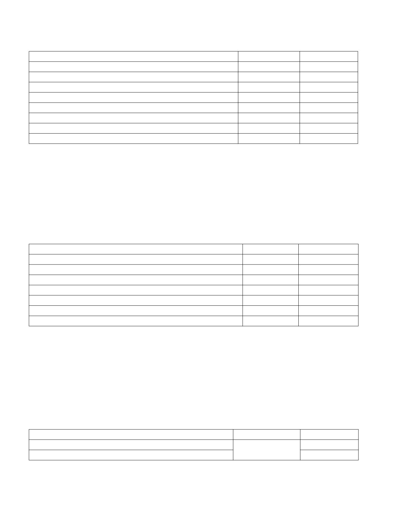
Table B-2. Encodings for 16-Bit Guest-State Fields (0000_10xx_xxxx_xxx0B)
Field Name
Index
Encoding
Guest ES selector
000000000B
00000800H
Guest CS selector
000000001B
00000802H
Guest SS selector
000000010B
00000804H
Vol. 3D B-1
FIELD ENCODING IN VMCS
Table B-2. Encodings for 16-Bit Guest-State Fields (0000_10xx_xxxx_xxx0B) (Contd.)
Field Name
Index
Encoding
Guest DS selector
000000011B
00000806H
Guest FS selector
000000100B
00000808H
Guest GS selector
000000101B
0000080AH
Guest LDTR selector
000000110B
0000080CH
Guest TR selector
000000111B
0000080EH
Guest interrupt status1
000001000B
00000810H
PML index2
000001001B
00000812H
Guest UINV3
000001010B
00000814H
NOTES:
1. This field exists only on processors that support the 1-setting of the “virtual-interrupt delivery” VM-execution control.
2. This field exists only on processors that support the 1-setting of the “enable PML” VM-execution control.
3. This field exists only on processors that support the 1-setting of either the “clear UINV” VM-exit control or the “load UINV” VM-entry
control.
B.1.3
16-Bit Host-State Fields
A value of 3 in bits 11:10 of an encoding indicates a field in the host-state area. These fields are distinguished by
their index value in bits 9:1. Table B-3 enumerates the 16-bit host-state fields.
Table B-3. Encodings for 16-Bit Host-State Fields (0000_11xx_xxxx_xxx0B)
Field Name
Index
Encoding
Host ES selector
000000000B
00000C00H
Host CS selector
000000001B
00000C02H
Host SS selector
000000010B
00000C04H
Host DS selector
000000011B
00000C06H
Host FS selector
000000100B
00000C08H
Host GS selector
000000101B
00000C0AH
Host TR selector
000000110B
00000C0CH
B.2
64-BIT FIELDS
A value of 1 in bits 14:13 of an encoding indicates a 64-bit field. There are 64-bit fields only for controls and for
guest state. As noted in Section 27.11.2, every 64-bit field has two encodings, which differ on bit 0, the access
type. Thus, each such field has an even encoding for full access and an odd encoding for high access.
B.2.1
64-Bit Control Fields
A value of 0 in bits 11:10 of an encoding indicates a control field. These fields are distinguished by their index value
in bits 9:1. Table B-4 enumerates the 64-bit control fields.
Table B-4. Encodings for 64-Bit Control Fields (0010_00xx_xxxx_xxxAb)
Field Name
Index
Encoding
Address of I/O bitmap A (full)
00002000H
000000000B
Address of I/O bitmap A (high)
00002001H
B-2
Vol. 3D

FIELD ENCODING IN VMCS
Table B-4. Encodings for 64-Bit Control Fields (0010_00xx_xxxx_xxxAb) (Contd.)
Field Name
Index
Encoding
Address of I/O bitmap B (full)
00002002H
000000001B
Address of I/O bitmap B (high)
00002003H
Address of MSR bitmaps (full)1
00002004H
000000010B
Address of MSR bitmaps (high)1
00002005H
VM-exit MSR-store address (full)
00002006H
000000011B
VM-exit MSR-store address (high)
00002007H
VM-exit MSR-load address (full)
00002008H
000000100B
VM-exit MSR-load address (high)
00002009H
VM-entry MSR-load address (full)
0000200AH
000000101B
VM-entry MSR-load address (high)
0000200BH
Executive-VMCS pointer (full)
0000200CH
000000110B
Executive-VMCS pointer (high)
0000200DH
PML address (full)2
0000200EH
000000111B
PML address (high)2
0000200FH
TSC offset (full)
00002010H
000001000B
TSC offset (high)
00002011H
Virtual-APIC address (full)3
00002012H
000001001B
Virtual-APIC address (high)3
00002013H
APIC-access address (full)4
00002014H
000001010B
APIC-access address (high)4
00002015H
Posted-interrupt descriptor address (full)5
00002016H
000001011B
Posted-interrupt descriptor address (high)5
00002017H
VM-function controls (full)6
00002018H
000001100B
VM-function controls (high)6
00002019H
EPT pointer (EPTP; full)7
0000201AH
000001101B
EPT pointer (EPTP; high)7
0000201BH
EOI-exit bitmap 0 (EOI_EXIT0; full)8
0000201CH
000001110B
EOI-exit bitmap 0 (EOI_EXIT0; high)8
0000201DH
EOI-exit bitmap 1 (EOI_EXIT1; full)8
0000201EH
000001111B
EOI-exit bitmap 1 (EOI_EXIT1; high)8
0000201FH
EOI-exit bitmap 2 (EOI_EXIT2; full)8
00002020H
000010000B
EOI-exit bitmap 2 (EOI_EXIT2; high)8
00002021H
EOI-exit bitmap 3 (EOI_EXIT3; full)8
00002022H
000010001B
EOI-exit bitmap 3 (EOI_EXIT3; high)8
00002023H
EPTP-list address (full)9
00002024H
000010010B
EPTP-list address (high)9
00002025H
VMREAD-bitmap address (full)10
00002026H
000010011B
VMREAD-bitmap address (high)10
00002027H
Vol. 3D B-3

FIELD ENCODING IN VMCS
Table B-4. Encodings for 64-Bit Control Fields (0010_00xx_xxxx_xxxAb) (Contd.)
Field Name
Index
Encoding
VMWRITE-bitmap address (full)10
00002028H
000010100B
VMWRITE-bitmap address (high)10
00002029H
Virtualization-exception information address (full)11
0000202AH
000010101B
Virtualization-exception information address (high)11
0000202BH
XSS-exiting bitmap (full)12
0000202CH
000010110B
XSS-exiting bitmap (high)12
0000202DH
ENCLS-exiting bitmap (full)13
0000202EH
000010111B
ENCLS-exiting bitmap (high)13
0000202FH
Sub-page-permission-table pointer (full)14
00002030H
000011000B
Sub-page-permission-table pointer (high)14
00002031H
TSC multiplier (full)15
00002032H
000011001B
TSC multiplier (high)15
00002033H
Tertiary processor-based VM-execution controls (full)16
00002034H
000011010B
Tertiary processor-based VM-execution controls (high)16
00002035H
Low PASID directory address (full)17
00002038H
000011100B
Low PASID directory address (high)17
00002039H
High PASID directory address (full)17
0000203AH
000011101B
High PASID directory address (high)17
0000203BH
SEAM shared EPT pointer (full)18
0000203CH
000011110B
SEAM shared EPT pointer (high)18
0000203DH
PCONFIG-exiting bitmap (full)19
0000203EH
000011111B
PCONFIG-exiting bitmap (high)19
0000203FH
Hypervisor-managed linear-address translation pointer (HLATP; full)20
00002040H
000100000B
HLATP (high)20
00002041H
PID-pointer table address (full)21
00002042H
000100001B
PID-pointer table address (high)21
00002043H
Secondary VM-exit controls (full)22
00002044H
000100010B
Secondary VM-exit controls (high)22
00002045H
IA32_SPEC_CTRL mask (full)23
0000204AH
000100101B
IA32_SPEC_CTRL mask (high)23
0000204BH
IA32_SPEC_CTRL shadow (full)23
0000204CH
000100110B
IA32_SPEC_CTRL shadow (high)23
0000204DH
Guest deadline shadow (full)24
0000204EH
000100111B
Guest deadline shadow (high)24
0000204FH
Injected-event data (full)25
00002052H
000101001B
Injected-event data (high)25
00002053H
NOTES:
1. This field exists only on processors that support the 1-setting of the “use MSR bitmaps” VM-execution control.
2. This field exists only on processors that support the 1-setting of the “enable PML” VM-execution control.
B-4
Vol. 3D

FIELD ENCODING IN VMCS
3. This field exists only on processors that support the 1-setting of the “use TPR shadow” VM-execution control.
4. This field exists only on processors that support the 1-setting of the “virtualize APIC accesses” VM-execution control.
5. This field exists only on processors that support the 1-setting of the “process posted interrupts” VM-execution control.
6. This field exists only on processors that support the 1-setting of the “enable VM functions” VM-execution control.
7. This field exists only on processors that support the 1-setting of the “enable EPT” VM-execution control.
8. This field exists only on processors that support the 1-setting of the “virtual-interrupt delivery” VM-execution control.
9. This field exists only on processors that support the 1-setting of the “EPTP switching” VM-function control.
10. This field exists only on processors that support the 1-setting of the “VMCS shadowing” VM-execution control.
11. This field exists only on processors that support the 1-setting of the “EPT-violation #VE” VM-execution control.
12. This field exists only on processors that support the 1-setting of the “enable XSAVES/XRSTORS” VM-execution control.
13. This field exists only on processors that support the 1-setting of the “enable ENCLS exiting” VM-execution control.
14. This field exists only on processors that support the 1-setting of the “sub-page write permissions for EPT” VM-execution control.
15. This field exists only on processors that support the 1-setting of the “use TSC scaling” VM-execution control.
16. This field exists only on processors that support the 1-setting of the “activate tertiary controls” VM-execution control.
17. This field exists only on processors that support the 1-setting of the “PASID translation” VM-execution control.
18. This field exists only on processors that support the 1-setting of the “SEAM guest-physical address width” VM-execution control.
19. This field exists only on processors that support the 1-setting of the “enable PCONFIG” VM-execution control.
20. This field exists only on processors that support the 1-setting of the “enable HLAT” VM-execution control.
21. This field exists only on processors that support the 1-setting of the “IPI virtualization” VM-execution control.
22. This field exists only on processors that support the 1-setting of the “activate secondary controls” VM-exit control.
23. This field exists only on processors that support the 1-setting of the “virtualize IA32_SPEC_CTRL” VM-execution control.
24. This field exists only on processors that support the 1-setting of the “APIC-timer virtualization” VM-execution control.
25. This field exists only on processors that support FRED transitions.
B.2.2
64-Bit Read-Only Data Fields
A value of 1 in bits 11:10 of an encoding indicates a read-only data field. These fields are distinguished by their
index value in bits 9:1. Table B-5 enumerates the 64-bit read-only data fields.
Table B-5. Encodings for 64-Bit Read-Only Data Fields (0010_01xx_xxxx_xxxAb)
Field Name
Index
Encoding
Guest-physical address (full)1
00002400H
000000000B
Guest-physical address (high)1
00002401H
MSR data (full)2
00002402H
000000001B
MSR data (high)2
00002403H
Original-event data (full)3
00002404H
000000010B
Original-event data (high)3
00002405H
NOTES:
1. This field exists only on processors that support the 1-setting of the “enable EPT” VM-execution control.
2. This field exists only on processors that support the 1-setting of the “enable MSR-list instructions” VM-execution control.
3. This field exists only on processors that support FRED transitions.
Vol. 3D B-5

FIELD ENCODING IN VMCS
B.2.3
64-Bit Guest-State Fields
A value of 2 in bits 11:10 of an encoding indicates a field in the guest-state area. These fields are distinguished by
their index value in bits 9:1. Table B-6 enumerates the 64-bit guest-state fields.
Table B-6. Encodings for 64-Bit Guest-State Fields (0010_10xx_xxxx_xxxAb)
Field Name
Index
Encoding
VMCS link pointer (full)
00002800H
000000000B
VMCS link pointer (high)
00002801H
Guest IA32_DEBUGCTL (full)
00002802H
000000001B
Guest IA32_DEBUGCTL (high)
00002803H
Guest IA32_PAT (full)1
00002804H
000000010B
Guest IA32_PAT (high)1
00002805H
Guest IA32_EFER (full)2
00002806H
000000011B
Guest IA32_EFER (high)2
00002807H
Guest IA32_PERF_GLOBAL_CTRL (full)3
00002808H
000000100B
Guest IA32_PERF_GLOBAL_CTRL (high)3
00002809H
Guest PDPTE0 (full)4
0000280AH
000000101B
Guest PDPTE0 (high)4
0000280BH
Guest PDPTE1 (full)4
0000280CH
000000110B
Guest PDPTE1 (high)4
0000280DH
Guest PDPTE2 (full)4
0000280EH
000000111B
Guest PDPTE2 (high)4
0000280FH
Guest PDPTE3 (full)4
00002810H
000001000B
Guest PDPTE3 (high)4
00002811H
Guest IA32_BNDCFGS (full)5
00002812H
000001001B
Guest IA32_BNDCFGS (high)5
00002813H
Guest IA32_RTIT_CTL (full)6
00002814H
000001010B
Guest IA32_RTIT_CTL (high)6
00002815H
Guest IA32_LBR_CTL (full)7
00002816H
000001011B
Guest IA32_LBR_CTL (high)7
00002817H
Guest IA32_PKRS (full)8
00002818H
000001100B
Guest IA32_PKRS (high)8
00002819H
Guest IA32_FRED_CONFIG (full)9
0000281AH
000001101B
Guest IA32_FRED_CONFIG (high)9
0000281BH
Guest IA32_FRED_RSP1 (full)9
0000281CH
000001110B
Guest IA32_FRED_RSP1 (high)9
0000281DH
Guest IA32_FRED_RSP2 (full)9
0000281EH
000001111B
Guest IA32_FRED_RSP2 (high)9
0000281FH
Guest IA32_FRED_RSP3 (full)9
00002820H
000010000B
Guest IA32_FRED_RSP3 (high)9
00002821H
B-6
Vol. 3D
FIELD ENCODING IN VMCS
Table B-6. Encodings for 64-Bit Guest-State Fields (0010_10xx_xxxx_xxxAb) (Contd.)
Field Name
Index
Encoding
Guest IA32_FRED_STKLVLS (full)9
00002822H
000010001B
Guest IA32_FRED_STKLVLS (high)9
00002823H
Guest IA32_FRED_SSP1 (full)9
00002824H
000010010B
Guest IA32_FRED_SSP1 (high)9
00002825H
Guest IA32_FRED_SSP2 (full)9
00002826H
000010011B
Guest IA32_FRED_SSP2 (high)9
00002827H
Guest IA32_FRED_SSP3 (full)9
00002828H
000010100B
Guest IA32_FRED_SSP3 (high)9
00002829H
Guest IA32_SPEC_CTRL (full)10
0000282EH
000010111B
Guest IA32_SPEC_CTRL (high)10
0000282FH
Guest deadline (full)11
00002830H
000011000B
Guest deadline (high)11
00002831H
NOTES:
1. This field exists only on processors that support either the 1-setting of the “load IA32_PAT” VM-entry control or that of the “save
IA32_PAT” VM-exit control.
2. This field exists only on processors that support either the 1-setting of the “load IA32_EFER” VM-entry control or that of the “save
IA32_EFER” VM-exit control.
3. This field exists only on processors that support the 1-setting of the “load IA32_PERF_GLOBAL_CTRL” VM-entry control.
4. This field exists only on processors that support the 1-setting of the “enable EPT” VM-execution control.
5. This field exists only on processors that support either the 1-setting of the “load IA32_BNDCFGS” VM-entry control or that of the
“clear IA32_BNDCFGS” VM-exit control.
6. This field exists only on processors that support either the 1-setting of the “load IA32_RTIT_CTL” VM-entry control or that of the
“clear IA32_RTIT_CTL” VM-exit control.
7. This field exists only on processors that support either the 1-setting of the “load IA32_LBR_CTL” VM-entry control or that of the
“clear IA32_LBR_CTL” VM-exit control.
8. This field exists only on processors that support the 1-setting of the “load PKRS” VM-entry control.
9. This field exists only on processors that support either the 1-setting of the “load FRED” VM-entry control or that of the “save FRED”
VM-exit control.
10. This field exists only on processors that support the 1-setting of the “load IA32_SPEC_CTRL” VM-entry control.
11. This field exists only on processors that support the 1-setting of the “APIC-timer virtualization” VM-execution control.
B.2.4
64-Bit Host-State Fields
A value of 3 in bits 11:10 of an encoding indicates a field in the host-state area. These fields are distinguished by
their index value in bits 9:1. Table B-7 enumerates the 64-bit control fields.
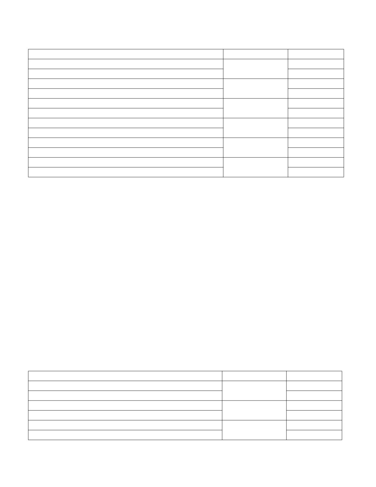
Table B-7. Encodings for 64-Bit Host-State Fields (0010_11xx_xxxx_xxxAb)
Field Name
Index
Encoding
Host IA32_PAT (full)1
00002C00H
000000000B
Host IA32_PAT (high)1
00002C01H
Host IA32_EFER (full)2
00002C02H
000000001B
Host IA32_EFER (high)2
00002C03H
Host IA32_PERF_GLOBAL_CTRL (full)3
00002C04H
000000010B
Host IA32_PERF_GLOBAL_CTRL (high)3
00002C05H
Vol. 3D B-7

FIELD ENCODING IN VMCS
Table B-7. Encodings for 64-Bit Host-State Fields (0010_11xx_xxxx_xxxAb) (Contd.)
Field Name
Index
Encoding
Host IA32_PKRS (full)4
00002C06H
000000011B
Host IA32_PKRS (high)4
00002C07H
Host IA32_FRED_CONFIG (full)5
00002C08H
000000100B
Host IA32_FRED_CONFIG (high)4
00002C09H
Host IA32_FRED_RSP1 (full)4
00002C0AH
000000101B
Host IA32_FRED_RSP1 (high)4
00002C0BH
Host IA32_FRED_RSP2 (full)4
00002C0CH
000000110B
Host IA32_FRED_RSP2 (high)4
00002C0DH
Host IA32_FRED_RSP3 (full)4
00002C0EH
000000111B
Host IA32_FRED_RSP3 (high)4
00002C0FH
Host IA32_FRED_STKLVLS (full)4
00002C10H
000001000B
Host IA32_FRED_STKLVLS (high)4
00002C11H
Host IA32_FRED_SSP1 (full)4
00002C12H
000001001B
Host IA32_FRED_SSP1 (high)4
00002C13H
Host IA32_FRED_SSP2 (full)4
00002C14H
000001010B
Host IA32_FRED_SSP2 (high)4
00002C15H
Host IA32_FRED_SSP3 (full)4
00002C16H
000001011B
Host IA32_FRED_SSP3 (high)4
00002C17H
IA32_SPEC_CTRL (full)6
00002C1AH
000001101B
IA32_SPEC_CTRL (high)6
00002C1BH
NOTES:
1. This field exists only on processors that support the 1-setting of the “load IA32_PAT” VM-exit control.
2. This field exists only on processors that support the 1-setting of the “load IA32_EFER” VM-exit control.
3. This field exists only on processors that support the 1-setting of the “load IA32_PERF_GLOBAL_CTRL” VM-exit control.
4. This field exists only on processors that support the 1-setting of the “load PKRS” VM-exit control.
5. This field exists only on processors that support the 1-setting of the “load FRED” VM-exit control.
6. This field exists only on processors that support the 1-setting of the “load IA32_SPEC_CTRL” VM-exit control.
B.3
32-BIT FIELDS
A value of 2 in bits 14:13 of an encoding indicates a 32-bit field. As noted in Section 27.11.2, each 32-bit field
allows only full access, meaning that bit 0 of its encoding is 0. Each such encoding is thus an even number.
B.3.1
32-Bit Control Fields
A value of 0 in bits 11:10 of an encoding indicates a control field. These fields are distinguished by their index value
in bits 9:1. Table B-8 enumerates the 32-bit control fields.
Table B-8. Encodings for 32-Bit Control Fields (0100_00xx_xxxx_xxx0B)
Field Name
Index
Encoding
Pin-based VM-execution controls
000000000B
00004000H
B-8
Vol. 3D

FIELD ENCODING IN VMCS
Table B-8. Encodings for 32-Bit Control Fields (0100_00xx_xxxx_xxx0B) (Contd.)
Field Name
Index
Encoding
Primary processor-based VM-execution controls
000000001B
00004002H
Exception bitmap
000000010B
00004004H
Page-fault error-code mask
000000011B
00004006H
Page-fault error-code match
000000100B
00004008H
CR3-target count
000000101B
0000400AH
Primary VM-exit controls
000000110B
0000400CH
VM-exit MSR-store count
000000111B
0000400EH
VM-exit MSR-load count
000001000B
00004010H
VM-entry controls
000001001B
00004012H
VM-entry MSR-load count
000001010B
00004014H
Injected-event identification1
000001011B
00004016H
Injected-event error code2
000001100B
00004018H
VM-entry instruction length
000001101B
0000401AH
TPR threshold3
000001110B
0000401CH
Secondary processor-based VM-execution controls4
000001111B
0000401EH
PLE_Gap5
000010000B
00004020H
PLE_Window5
000010001B
00004022H
Instruction-timeout control6
000010010B
00004024H
SEAM-guest KeyID7
000010011B
00004026H
NOTES:
1. Older versions of this document called this field VM-entry interruption information.
2. Older versions of this document called this field VM-entry error code.
3. This field exists only on processors that support the 1-setting of the “use TPR shadow” VM-execution control.
4. This field exists only on processors that support the 1-setting of the “activate secondary controls” VM-execution control.
5. This field exists only on processors that support the 1-setting of the “PAUSE-loop exiting” VM-execution control.
6. This field exists only on processors that support the 1-setting of the “instruction timeout” VM-execution control.
7. This field exists only on processors that support the 1-setting of the “SEAM guest-physical address width” VM-execution control.
B.3.2
32-Bit Read-Only Data Fields
A value of 1 in bits 11:10 of an encoding indicates a read-only data field. These fields are distinguished by their
index value in bits 9:1. Table B-9 enumerates the 32-bit read-only data fields.
Table B-9. Encodings for 32-Bit Read-Only Data Fields (0100_01xx_xxxx_xxx0B)
Field Name
Index
Encoding
VM-instruction error
000000000B
00004400H
Exit reason
000000001B
00004402H
Exiting-event identification1
000000010B
00004404H
Exiting-event error code2
000000011B
00004406H
Original-event identification3
000000100B
00004408H
Original-event error code4
000000101B
0000440AH
Vol. 3D B-9

FIELD ENCODING IN VMCS
Table B-9. Encodings for 32-Bit Read-Only Data Fields (0100_01xx_xxxx_xxx0B) (Contd.)
Field Name
Index
Encoding
VM-exit instruction length
000000110B
0000440CH
VM-exit instruction information
000000111B
0000440EH
NOTES:
1. Older versions of this document called this field VM-exit interruption information.
2. Older versions of this document called this field VM-exit interruption error code.
3. Older versions of this document called this field IDT-vectoring information.
4. Older versions of this document called this field IDT-vectoring error code.
B.3.3
32-Bit Guest-State Fields
A value of 2 in bits 11:10 of an encoding indicates a field in the guest-state area. These fields are distinguished by
their index value in bits 9:1. Table B-10 enumerates the 32-bit guest-state fields.
Table B-10. Encodings for 32-Bit Guest-State Fields (0100_10xx_xxxx_xxx0B)
Field Name
Index
Encoding
Guest ES limit
000000000B
00004800H
Guest CS limit
000000001B
00004802H
Guest SS limit
000000010B
00004804H
Guest DS limit
000000011B
00004806H
Guest FS limit
000000100B
00004808H
Guest GS limit
000000101B
0000480AH
Guest LDTR limit
000000110B
0000480CH
Guest TR limit
000000111B
0000480EH
Guest GDTR limit
000001000B
00004810H
Guest IDTR limit
000001001B
00004812H
Guest ES access rights
000001010B
00004814H
Guest CS access rights
000001011B
00004816H
Guest SS access rights
000001100B
00004818H
Guest DS access rights
000001101B
0000481AH
Guest FS access rights
000001110B
0000481CH
Guest GS access rights
000001111B
0000481EH
Guest LDTR access rights
000010000B
00004820H
Guest TR access rights
000010001B
00004822H
Guest interruptibility state
000010010B
00004824H
Guest activity state
000010011B
00004826H
Guest SMBASE
000010100B
00004828H
Guest IA32_SYSENTER_CS
000010101B
0000482AH
VMX-preemption timer value1
000010111B
0000482EH
NOTES:
1. This field exists only on processors that support the 1-setting of the “activate VMX-preemption timer” VM-execution control.
B-10
Vol. 3D

FIELD ENCODING IN VMCS
The limit fields for GDTR and IDTR are defined to be 32 bits in width even though these fields are only 16-bits wide
in the Intel 64 and IA-32 architectures. VM entry ensures that the high 16 bits of both these fields are cleared to 0.
B.3.4
32-Bit Host-State Field
A value of 3 in bits 11:10 of an encoding indicates a field in the host-state area. There is only one such 32-bit field
as given in Table B-11.
Table B-11. Encoding for 32-Bit Host-State Field (0100_11xx_xxxx_xxx0B)
Field Name
Index
Encoding
Host IA32_SYSENTER_CS
000000000B
00004C00H
B.4
NATURAL-WIDTH FIELDS
A value of 3 in bits 14:13 of an encoding indicates a natural-width field. As noted in Section 27.11.2, each of these
fields allows only full access, meaning that bit 0 of its encoding is 0. Each such encoding is thus an even number.
B.4.1
Natural-Width Control Fields
A value of 0 in bits 11:10 of an encoding indicates a control field. These fields are distinguished by their index value
in bits 9:1. Table B-12 enumerates the natural-width control fields.
Table B-12. Encodings for Natural-Width Control Fields (0110_00xx_xxxx_xxx0B)
Field Name
Index
Encoding
CR0 guest/host mask
000000000B
00006000H
CR4 guest/host mask
000000001B
00006002H
CR0 read shadow
000000010B
00006004H
CR4 read shadow
000000011B
00006006H
CR3-target value 0
000000100B
00006008H
CR3-target value 1
000000101B
0000600AH
CR3-target value 2
000000110B
0000600CH
CR3-target value 31
000000111B
0000600EH
NOTES:
1. If a future implementation supports more than 4 CR3-target values, they will be encoded consecutively following the 4 encodings
given here.
B.4.2
Natural-Width Read-Only Data Fields
A value of 1 in bits 11:10 of an encoding indicates a read-only data field. These fields are distinguished by their
index value in bits 9:1. Table B-13 enumerates the natural-width read-only data fields.
Table B-13. Encodings for Natural-Width Read-Only Data Fields (0110_01xx_xxxx_xxx0B)
Field Name
Index
Encoding
Exit qualification
000000000B
00006400H
I/O RCX
000000001B
00006402H
I/O RSI
000000010B
00006404H
Vol. 3D B-11

FIELD ENCODING IN VMCS
Table B-13. Encodings for Natural-Width Read-Only Data Fields (0110_01xx_xxxx_xxx0B) (Contd.)
Field Name
Index
Encoding
I/O RDI
000000011B
00006406H
I/O RIP
000000100B
00006408H
Guest-linear address
000000101B
0000640AH
B.4.3
Natural-Width Guest-State Fields
A value of 2 in bits 11:10 of an encoding indicates a field in the guest-state area. These fields are distinguished by
their index value in bits 9:1. Table B-14 enumerates the natural-width guest-state fields.
Table B-14. Encodings for Natural-Width Guest-State Fields (0110_10xx_xxxx_xxx0B)
Field Name
Index
Encoding
Guest CR0
000000000B
00006800H
Guest CR3
000000001B
00006802H
Guest CR4
000000010B
00006804H
Guest ES base
000000011B
00006806H
Guest CS base
000000100B
00006808H
Guest SS base
000000101B
0000680AH
Guest DS base
000000110B
0000680CH
Guest FS base
000000111B
0000680EH
Guest GS base
000001000B
00006810H
Guest LDTR base
000001001B
00006812H
Guest TR base
000001010B
00006814H
Guest GDTR base
000001011B
00006816H
Guest IDTR base
000001100B
00006818H
Guest DR7
000001101B
0000681AH
Guest RSP
000001110B
0000681CH
Guest RIP
000001111B
0000681EH
Guest RFLAGS
000010000B
00006820H
Guest pending debug exceptions
000010001B
00006822H
Guest IA32_SYSENTER_ESP
000010010B
00006824H
Guest IA32_SYSENTER_EIP
000010011B
00006826H
Guest IA32_S_CET1
000010100B
00006828H
Guest SSP1
000010101B
0000682AH
Guest IA32_INTERRUPT_SSP_TABLE_ADDR1
000010110B
0000682CH
NOTES:
1. This field is supported only on processors that support the 1-setting of the “load CET state” VM-entry control.
The base-address fields for ES, CS, SS, and DS in the guest-state area are defined to be natural-width (with 64 bits
on processors supporting Intel 64 architecture) even though these fields are only 32-bits wide in the Intel 64 archi-
tecture. VM entry ensures that the high 32 bits of these fields are cleared to 0.
B-12
Vol. 3D

FIELD ENCODING IN VMCS
B.4.4
Natural-Width Host-State Fields
A value of 3 in bits 11:10 of an encoding indicates a field in the host-state area. These fields are distinguished by
their index value in bits 9:1. Table B-15 enumerates the natural-width host-state fields.
Table B-15. Encodings for Natural-Width Host-State Fields (0110_11xx_xxxx_xxx0B)
Field Name
Index
Encoding
Host CR0
000000000B
00006C00H
Host CR3
000000001B
00006C02H
Host CR4
000000010B
00006C04H
Host FS base
000000011B
00006C06H
Host GS base
000000100B
00006C08H
Host TR base
000000101B
00006C0AH
Host GDTR base
000000110B
00006C0CH
Host IDTR base
000000111B
00006C0EH
Host IA32_SYSENTER_ESP
000001000B
00006C10H
Host IA32_SYSENTER_EIP
000001001B
00006C12H
Host RSP
000001010B
00006C14H
Host RIP
000001011B
00006C16H
Host IA32_S_CET1
000001100B
00006C18H
Host SSP1
000001101B
00006C1AH
Host IA32_INTERRUPT_SSP_TABLE_ADDR1
000001110B
00006C1CH
NOTES:
1. This field is supported only on processors that support the 1-setting of the “load CET state” VM-exit control.
Vol. 3D B-13
FIELD ENCODING IN VMCS
B-14
Vol. 3D

APPENDIX C
VMX BASIC EXIT REASONS
Every VM exit writes a 32-bit exit reason to the VMCS (see Section 27.9.1). Certain VM-entry failures also do this
(see Section 29.8). The low 16 bits of the exit-reason field form the basic exit reason which provides basic informa-
tion about the cause of the VM exit or VM-entry failure.
Table C-1 lists values for basic exit reasons and explains their meaning. Entries apply to VM exits, unless otherwise
noted.
Table C-1. Basic Exit Reasons
Basic Exit
Reason
Description
0
Exception or non-maskable interrupt (NMI). Either:
1: Guest software caused an exception and the bit in the exception bitmap associated with exception’s vector was
1. This case includes executions of BOUND that cause #BR, executions of INT1 (they cause #DB), executions of
INT3 (they cause #BP), executions of INTO that cause #OF, and executions of UD0, UD1, UD2, and UDB (they
cause #UD).
2: An NMI was delivered to the logical processor and the “NMI exiting” VM-execution control was 1.
1
External interrupt. An external interrupt arrived and the “external-interrupt exiting” VM-execution control was 1.
2
Triple fault. The logical processor encountered an exception while attempting to call the double-fault handler and
that exception did not itself cause a VM exit due to the exception bitmap.
3
INIT signal. An INIT signal arrived
4
Start-up IPI (SIPI). A SIPI arrived while the logical processor was in the “wait-for-SIPI” state.
5
I/O system-management interrupt (SMI). An SMI arrived immediately after retirement of an I/O instruction and
caused an SMM VM exit (see Section 34.15.2).
6
Other SMI. An SMI arrived and caused an SMM VM exit (see Section 34.15.2) but not immediately after retirement of
an I/O instruction.
7
Interrupt window. At the beginning of an instruction, RFLAGS.IF was 1; events were not blocked by STI or by MOV
SS; and the “interrupt-window exiting” VM-execution control was 1.
8
NMI window. At the beginning of an instruction, there was no virtual-NMI blocking; events were not blocked by MOV
SS; and the “NMI-window exiting” VM-execution control was 1.
9
Task switch. Guest software attempted a task switch.
10
CPUID. Guest software attempted to execute CPUID.
11
GETSEC. Guest software attempted to execute GETSEC.
12
HLT. Guest software attempted to execute HLT and the “HLT exiting” VM-execution control was 1.
13
INVD. Guest software attempted to execute INVD.
14
INVLPG. Guest software attempted to execute INVLPG and the “INVLPG exiting” VM-execution control was 1.
15
RDPMC. Guest software attempted to execute RDPMC and the “RDPMC exiting” VM-execution control was 1.
16
RDTSC. Guest software attempted to execute RDTSC and the “RDTSC exiting” VM-execution control was 1.
17
RSM. Guest software attempted to execute RSM in SMM.
18
VMCALL. VMCALL was executed either by guest software (causing an ordinary VM exit) or by the executive monitor
(causing an SMM VM exit; see Section 34.15.2).
19
VMCLEAR. Guest software attempted to execute VMCLEAR.
20
VMLAUNCH. Guest software attempted to execute VMLAUNCH.
21
VMPTRLD. Guest software attempted to execute VMPTRLD.
22
VMPTRST. Guest software attempted to execute VMPTRST.
Vol. 3D C-1

VMX BASIC EXIT REASONS
Table C-1. Basic Exit Reasons (Contd.)
Basic Exit
Reason
Description
23
VMREAD. Guest software attempted to execute VMREAD.
24
VMRESUME. Guest software attempted to execute VMRESUME.
25
VMWRITE. Guest software attempted to execute VMWRITE.
26
VMXOFF. Guest software attempted to execute VMXOFF.
27
VMXON. Guest software attempted to execute VMXON.
28
Control-register accesses. Guest software attempted to access CR0, CR3, CR4, or CR8 using CLTS, LMSW, or
MOV CR and the VM-execution control fields indicate that a VM exit should occur (see Section 28.1 for details). This
basic exit reason is not used for trap-like VM exits following executions of the MOV to CR8 instruction when the “use
TPR shadow” VM-execution control is 1. Such VM exits instead use basic exit reason 43.
29
MOV DR. Guest software attempted a MOV to or from a debug register and the “MOV-DR exiting” VM-execution
control was 1.
30
I/O instruction. Guest software attempted to execute an I/O instruction and either:
1: The “use I/O bitmaps” VM-execution control was 0 and the “unconditional I/O exiting” VM-execution control was 1.
2: The “use I/O bitmaps” VM-execution control was 1 and a bit in the I/O bitmap associated with one of the ports
accessed by the I/O instruction was 1.
31
RDMSR (implicit form). Guest software attempted to execute RDMSR and one of the following holds:
• The “use MSR bitmaps” VM-execution control was 0.
• The value of ECX is neither in the range 00000000H - 00001FFFH nor in the range C0000000H - C0001FFFH.
• The value of ECX is in the range 00000000H - 00001FFFH and the nth bit in read bitmap for low MSRs is 1,
where n is the value of ECX.
• The value of ECX is in the range C0000000H - C0001FFFH and the nth bit in read bitmap for high MSRs is 1,
where n is the value of ECX & 00001FFFH.
32
WRMSR (implicit form) or WRMSRNS. Guest software attempted to execute either WRMSR or WRMSRNS and
either:
1: The “use MSR bitmaps” VM-execution control was 0.
2: The value of ECX is neither in the range 00000000H - 00001FFFH nor in the range C0000000H - C0001FFFH.
3: The value of ECX is in the range 00000000H - 00001FFFH and the nth bit in write bitmap for low MSRs is 1, where
n is the value of ECX.
4: The value of ECX is in the range C0000000H - C0001FFFH and the nth bit in write bitmap for high MSRs is 1,
where n is the value of ECX & 00001FFFH.
33
VM-entry failure due to invalid guest state. A VM entry failed one of the checks identified in Section 29.3.1.
34
VM-entry failure due to MSR loading. A VM entry failed in an attempt to load MSRs. See Section 29.4.
36
MWAIT. Guest software attempted to execute MWAIT and the “MWAIT exiting” VM-execution control was 1.
37
Monitor trap flag. A VM exit occurred due to the 1-setting of the “monitor trap flag” VM-execution control (see
Section 28.5.2) or VM entry injected a pending MTF VM exit as part of VM entry (see Section 29.6.2).
39
MONITOR. Guest software attempted to execute MONITOR and the “MONITOR exiting” VM-execution control was 1.
40
PAUSE. Either guest software attempted to execute PAUSE and the “PAUSE exiting” VM-execution control was 1 or
the “PAUSE-loop exiting” VM-execution control was 1 and guest software executed a PAUSE loop with execution
time exceeding PLE_Window (see Section 28.1.3).
41
VM-entry failure due to machine-check event. A machine-check event occurred during VM entry (see Section
29.9).
43
TPR below threshold. The logical processor determined that the value of bits 7:4 of the byte at offset 080H on the
virtual-APIC page was below that of the TPR threshold VM-execution control field while the “use TPR shadow” VM-
execution control was 1 either as part of TPR virtualization (Section 32.1.2) or VM entry (Section 29.7.7).
44
APIC access. Guest software attempted to access memory at a physical address on the APIC-access page and the
“virtualize APIC accesses” VM-execution control was 1 (see Section 32.4).
45
Virtualized EOI. EOI virtualization was performed for a virtual interrupt whose vector indexed a bit set in the EOI-
exit bitmap.
C-2
Vol. 3D

VMX BASIC EXIT REASONS
Table C-1. Basic Exit Reasons (Contd.)
Basic Exit
Reason
Description
46
Access to GDTR or IDTR. Guest software attempted to execute LGDT, LIDT, SGDT, or SIDT and the “descriptor-table
exiting” VM-execution control was 1.
47
Access to LDTR or TR. Guest software attempted to execute LLDT, LTR, SLDT, or STR and the “descriptor-table
exiting” VM-execution control was 1.
48
EPT violation. An attempt to access memory with a guest-physical address was disallowed by the configuration of
the EPT paging structures.
49
EPT misconfiguration. An attempt to access memory with a guest-physical address encountered a misconfigured
EPT paging-structure entry.
50
INVEPT. Guest software attempted to execute INVEPT.
51
RDTSCP. Guest software attempted to execute RDTSCP and the “enable RDTSCP” and “RDTSC exiting” VM-execution
controls were both 1.
52
VMX-preemption timer expired. The preemption timer counted down to zero.
53
INVVPID. Guest software attempted to execute INVVPID.
54
WBINVD or WBNOINVD. Guest software attempted to execute WBINVD or WBNOINVD and the “WBINVD exiting”
VM-execution control was 1.
55
XSETBV. Guest software attempted to execute XSETBV.
56
APIC write. Guest software completed a write to the virtual-APIC page that must be virtualized by VMM software
(see Section 32.4.3.3).
57
RDRAND. Guest software attempted to execute RDRAND and the “RDRAND exiting” VM-execution control was 1.
58
INVPCID. Guest software attempted to execute INVPCID and the “enable INVPCID” and “INVLPG exiting”
VM-execution controls were both 1.
59
VMFUNC. Guest software invoked a VM function with the VMFUNC instruction and the VM function either was not
enabled or generated a function-specific condition causing a VM exit.
60
ENCLS. Guest software attempted to execute ENCLS, “enable ENCLS exiting” VM-execution control was 1, and either
(1) EAX < 63 and the corresponding bit in the ENCLS-exiting bitmap is 1; or (2) EAX ? 63 and bit 63 in the ENCLS-
exiting bitmap is 1.
61
RDSEED. Guest software attempted to execute RDSEED and the “RDSEED exiting” VM-execution control was 1.
62
Page-modification log full. The processor attempted to create a page-modification log entry and the value of the
PML index was not in the range 0-511.
63
XSAVES. Guest software attempted to execute XSAVES, the “enable XSAVES/XRSTORS” was 1, and a bit was set in
the logical-AND of the following three values: EDX:EAX, the IA32_XSS MSR, and the XSS-exiting bitmap.
64
XRSTORS. Guest software attempted to execute XRSTORS, the “enable XSAVES/XRSTORS” was 1, and a bit was set
in the logical-AND of the following three values: EDX:EAX, the IA32_XSS MSR, and the XSS-exiting bitmap.
65
PCONFIG. Guest software attempted to execute PCONFIG, “enable PCONFIG” VM-execution control was 1, and either
(1) EAX < 63 and the corresponding bit in the PCONFIG-exiting bitmap is 1; or (2) EAX ? 63 and bit 63 in the
PCONFIG-exiting bitmap is 1.
66
SPP-related event. The processor attempted to determine an access’s sub-page write permission and encountered
an SPP miss or an SPP misconfiguration. See Section 31.3.4.2.
67
UMWAIT. Guest software attempted to execute UMWAIT and the “enable user wait and pause” and “RDTSC exiting”
VM-execution controls were both 1.
68
TPAUSE. Guest software attempted to execute TPAUSE and the “enable user wait and pause” and “RDTSC exiting”
VM-execution controls were both 1.
69
LOADIWKEY. Guest software attempted to execute LOADIWKEY and the “LOADIWKEY exiting” VM-execution control
was 1.
72
ENQCMD PASID translation failure. A VM exit occurred during PASID translation because the present bit was clear
in a PASID-directory entry, the valid bit was clear in a PASID-table entry, or one of the entries set a reserved bit.
Vol. 3D C-3

VMX BASIC EXIT REASONS
Table C-1. Basic Exit Reasons (Contd.)
Basic Exit
Reason
Description
73
ENQCMDS PASID translation failure. A VM exit occurred during PASID translation because the present bit was clear
in a PASID-directory entry, the valid bit was clear in a PASID-table entry, or one of the entries set a reserved bit.
74
Bus lock. The processor asserted a bus lock while the “bus-lock detection” VM-execution control was 1. (Such
VM exits will also set bit 26 of the exit-reason field.)
75
Instruction timeout. The “instruction timeout” VM-execution control was 1 and certain operations prevented the
processor from reaching an instruction boundary within the amount of time specified by the instruction-timeout
control.
76
SEAMCALL. Guest software attempted to execute SEAMCALL.
77
TDCALL. Guest software attempted to execute TDCALL.
78
RDMSRLIST. Guest software attempted to execute RDMSRLIST and either the “use MSR bitmaps” VM-execution
control was 0 or any of the following holds for the address of an MSR being accessed:
• The address is neither in the range 00000000H - 00001FFFH nor in the range C0000000H - C0001FFFH.
• The address is in the range 00000000H - 00001FFFH and the nth bit in read bitmap for low MSRs is 1, where n is
the address.
• The address is in the range C0000000H - C0001FFFH and the nth bit in read bitmap for high MSRs is 1, where n
is the logical AND of the address and the value 00001FFFH.
79
WRMSRLIST. Guest software attempted to execute WRMSRLIST and either the “use MSR bitmaps” VM-execution
control was 0 or any of the following holds for the address of an MSR being accessed:
• The address is neither in the range 00000000H - 00001FFFH nor in the range C0000000H - C0001FFFH.
• The address is in the range 00000000H - 00001FFFH and the nth bit in write bitmap for low MSRs is 1, where n
is the address.
• The address is in the range C0000000H - C0001FFFH and the nth bit in write bitmap for high MSRs is 1, where n
is the logical AND of the address and the value 00001FFFH.
80
URDMSR. Guest software attempted to execute URDMSR and one of the following holds:
• The “use MSR bitmaps” VM-execution control is 0.
• The MSR address is in the range 0000H-1FFFH and bit n is 1 in the read bitmap for low MSRs (referenced by an
address in the VMCS), where n is the MSR address.
• The MSR address is in the range 2000H-3FFFH.
81
UWRMSR. Guest software attempted to execute UWRMSR and one of the following holds:
• The “use MSR bitmaps” VM-execution control is 0.
• The MSR address is in the range 0000H-1FFFH, and bit n is 1 in the write bitmap for low MSRs (referenced by an
address in the VMCS), where n is the MSR address.
• The MSR address is in the range 2000H-3FFFH.
84
RDMSR (immediate form). Guest software attempted to execute RDMSR and one of the following holds:
• The “use MSR bitmaps” VM-execution control was 0.
• The MSR address is neither in the range 00000000H - 00001FFFH nor in the range C0000000H - C0001FFFH.
• The MSR address is in the range 00000000H - 00001FFFH and the nth bit in read bitmap for low MSRs is 1,
where n is the MSR address.
• The MSR address is in the range C0000000H - C0001FFFH and the nth bit in read bitmap for high MSRs is 1,
where n is the logical AND of the MSR address and the value of 00001FFFH.
85
WRMSRNS (immediate form). Guest software attempted to execute either WRMSR or WRMSRNS and either:
1: The “use MSR bitmaps” VM-execution control was 0.
2: The MSR address is neither in the range 00000000H - 00001FFFH nor in the range C0000000H - C0001FFFH.
3: The MSR address is in the range 00000000H - 00001FFFH and the nth bit in write bitmap for low MSRs is 1,
where n is the MSR address.
4: The MSR address is in the range C0000000H - C0001FFFH and the nth bit in write bitmap for high MSRs is 1,
where n is the logical AND of the MSR address and the value of 00001FFFH.
C-4
Vol. 3D

Intel® 64 and IA-32 Architectures
Software Developer’s Manual
Volume 4:
Model-Specific Registers
NOTE: The Intel® 64 and IA-32 Architectures Software Developer's Manual consists of ten volumes:
Basic Architecture, Order Number 253665; Instruction Set Reference, A-L, Order Number 253666;
Instruction Set Reference, M-U, Order Number 253667; Instruction Set Reference, V, Order Number
326018; Instruction Set Reference, W-Z, Order Number 334569; System Programming Guide, Part 1,
Order Number 253668; System Programming Guide, Part
2, Order Number 253669; System
Programming Guide, Part 3, Order Number 326019; System Programming Guide, Part 4, Order Number
332831; Model-Specific Registers, Order Number 335592. Refer to all ten volumes when evaluating
your design needs.
Order Number: 335592-092US
June 2026
Notices & Disclaimers
Intel technologies may require enabled hardware, software or service activation.
No product or component can be absolutely secure.
Your costs and results may vary.
You may not use or facilitate the use of this document in connection with any infringement or other legal analysis concerning
Intel products described herein. You agree to grant Intel a non-exclusive, royalty-free license to any patent claim thereafter
drafted which includes subject matter disclosed herein.
All product plans and roadmaps are subject to change without notice.
The products described may contain design defects or errors known as errata which may cause the product to deviate from
published specifications. Current characterized errata are available on request.
Intel disclaims all express and implied warranties, including without limitation, the implied warranties of merchantability,
fitness for a particular purpose, and non-infringement, as well as any warranty arising from course of performance, course of
dealing, or usage in trade.
Code names are used by Intel to identify products, technologies, or services that are in development and not publicly
available. These are not “commercial” names and not intended to function as trademarks.
No license (express or implied, by estoppel or otherwise) to any intellectual property rights is granted by this document, with
the sole exception that a) you may publish an unmodified copy and b) code, identified as Sample Code in this document is
licensed subject to the Zero-Clause BSD open source license (0BSD), https://opensource.org/licenses/0BSD. You may create
software implementations based on this document and in compliance with the foregoing that are intended to execute on the
Intel product(s) referenced in this document. No rights are granted to create modifications or derivatives of this document.
© Intel Corporation. Intel, the Intel logo, and other Intel marks are trademarks of Intel Corporation or its subsidiaries. Other
names and brands may be claimed as the property of others.
CONTENTS
PAGE
CHAPTER 1
ABOUT THIS MANUAL
1.1
OVERVIEW OF THE MODEL-SPECIFIC REGISTERS
1-1
CHAPTER 2
MODEL-SPECIFIC REGISTERS (MSRS)
2.1
ARCHITECTURAL MSRS
2-3
2.2
MSRS IN THE INTEL® CORE™ 2 PROCESSOR FAMILY
2-94
2.3
MSRS IN THE 45 NM AND 32 NM INTEL ATOM® PROCESSOR FAMILY
2-110
2.4
MSRS IN INTEL PROCESSORS BASED ON SILVERMONT MICROARCHITECTURE
2-123
2.4.1
MSRs with Model-Specific Behavior in the Silvermont Microarchitecture
2-139
2.4.2
MSRs in Intel Atom® Processors Based on Airmont Microarchitecture
2-142
2.5
MSRS IN INTEL ATOM® PROCESSORS BASED ON GOLDMONT MICROARCHITECTURE
2-144
2.6
MSRS IN INTEL ATOM® PROCESSORS BASED ON GOLDMONT PLUS MICROARCHITECTURE
2-170
2.7
MSRS IN INTEL ATOM® PROCESSORS BASED ON TREMONT MICROARCHITECTURE
2-175
2.8
MSRS IN PROCESSORS BASED ON NEHALEM MICROARCHITECTURE
2-177
2.8.1
Additional MSRs in the Intel® Xeon® Processor 5500 and 3400 Series
2-199
2.8.2
Additional MSRs in the Intel® Xeon® Processor 7500 Series
2-201
2.9
MSRS IN THE INTEL® XEON® PROCESSOR 5600 SERIES BASED ON WESTMERE MICROARCHITECTURE
2-221
2.10
MSRS IN THE INTEL® XEON® PROCESSOR E7 FAMILY BASED ON WESTMERE MICROARCHITECTURE
2-222
2.11
MSRS IN THE INTEL® PROCESSOR FAMILY BASED ON SANDY BRIDGE MICROARCHITECTURE
2-225
2.11.1
MSRs in the 2nd Generation Intel® Core™ Processor Family Based on Sandy Bridge Microarchitecture
2-247
2.11.2
MSRs in the Intel® Xeon® Processor E5 Family Based on Sandy Bridge Microarchitecture
2-253
2.11.3
Additional Uncore PMU MSRs in the Intel® Xeon® Processor E5 Family
2-258
2.12
MSRS IN THE 3RD GENERATION INTEL® CORE™ PROCESSOR FAMILY BASED ON IVY BRIDGE MICROARCHITECTURE. . . 2-264
2.12.1
MSRs in the Intel® Xeon® Processor E5 v2 Product Family Based on Ivy Bridge-E Microarchitecture
2-267
2.12.2
Additional MSRs Supported by the Intel® Xeon® Processor E7 v2 Family
2-279
2.12.3
Additional Uncore PMU MSRs in the Intel® Xeon® Processor E5 v2 and E7 v2 Families
2-282
2.13
MSRS IN THE 4TH GENERATION INTEL® CORE™ PROCESSORS BASED ON HASWELL MICROARCHITECTURE
2-288
2.13.1
MSRs in the 4th Generation Intel® Core™ Processor Family Based on Haswell Microarchitecture
2-293
2.13.2
Additional Residency MSRs Supported in 4th Generation Intel® Core™ Processors
2-304
2.14
MSRS IN THE INTEL® XEON® PROCESSOR E5 V3 AND E7 V3 PRODUCT FAMILY
2-305
2.14.1
Additional Uncore PMU MSRs in the Intel® Xeon® Processor E5 v3 Family
2-318
2.15
MSRS IN THE INTEL® CORE™ M PROCESSORS AND THE 5TH GENERATION INTEL® CORE™ PROCESSORS
2-333
2.16
MSRS IN THE INTEL® XEON® PROCESSOR E5 V4 FAMILY
2-337
2.16.1
Additional MSRs Supported in the Intel® Xeon® Processor D Product Family
2-348
2.16.2
Additional MSRs Supported in Intel® Xeon® Processors E5 v4 and E7 v4 Families
2-351
2.17
MSRS IN THE 6TH-13TH GENERATION INTEL® CORE™ PROCESSORS, 1ST-5TH GENERATION
INTEL® XEON® SCALABLE PROCESSOR FAMILIES, INTEL® CORE™ ULTRA 7 PROCESSORS, 8TH GENERATION
INTEL® CORE™ I3 PROCESSORS, INTEL® XEON® E PROCESSORS, INTEL® XEON® 6 P-CORE PROCESSORS,
INTEL® XEON® 6 E-CORE PROCESSORS, AND INTEL® SERIES 2 CORE™ ULTRA PROCESSORS
2-359
2.17.1
MSRs Introduced in 7th Generation and 8th Generation Intel® Core™ Processors Based on
Kaby Lake Microarchitecture and Coffee Lake Microarchitecture
2-384
2.17.2
MSRs Specific to 8th Generation Intel® Core™ i3 Processors
2-386
2.17.3
MSRs Introduced in 10th Generation Intel® Core™ Processors
2-393
2.17.4
MSRs Introduced in the 11th Generation Intel® Core™ Processors based on Tiger Lake Microarchitecture
2-397
2.17.5
MSRs Introduced in the 12th and 13th Generation Intel® Core™ Processors Supporting Performance
Hybrid Architecture
2-400
2.17.6
MSRs Introduced in the Intel® Xeon® Scalable Processor Family
2-410
2.17.7
MSRs Specific to the 3rd Generation Intel® Xeon® Scalable Processor Family Based on Ice Lake Microarchitecture . .2-426
2.17.8
MSRs Specific to the 4th and 5th Generation Intel® Xeon® Scalable Processor Families
2-428
2.17.9
MSRs Introduced in the Intel® Core™ Ultra 7 Processor Supporting Performance Hybrid Architecture
2-440
2.17.10
MSRs Introduced in the Intel® Xeon® 6 P-Core Processors
2-464
2.17.11
MSRs Introduced in the Intel® Xeon® 6 E-Core Processors
2-483
2.17.12
MSRs Introduced in the Intel® Series 2 Core™ Ultra Processor Supporting Performance Hybrid Architecture
2-498
2.18
MSRS IN THE INTEL® XEON PHI™ PROCESSOR 3200/5200/7200 SERIES AND THE INTEL® XEON PHI™ PROCESSOR
7215/7285/7295 SERIES
2-508
2.19
MSRS IN THE PENTIUM® 4 AND INTEL® XEON® PROCESSORS
2-528
2.19.1
MSRs Unique to Intel® Xeon® Processor MP with L3 Cache
2-554
Vol. 4
iii
CONTENTS
PAGE
2.20
MSRS IN INTEL® CORE™ SOLO AND INTEL® CORE™ DUO PROCESSORS
2-555
2.21
MSRS IN THE PENTIUM M PROCESSOR
2-566
2.22
MSRS IN THE P6 FAMILY PROCESSORS
2-573
2.23
MSRS IN PENTIUM PROCESSORS
2-583
iv Vol. 4
CONTENTS
PAGE
FIGURES
Vol. 4 v
CONTENTS
PAGE
TABLES
Table 2-1.
CPUID Signature Values of DisplayFamily_DisplayModel
2-1
Table 2-2.
IA-32 Architectural MSRs
2-4
Table 2-3.
MSRs in Processors Based on Intel® Core™ Microarchitecture
2-94
Table 2-4.
MSRs in the 45 nm and 32 nm Intel Atom® Processor Family
2-110
Table 2-5.
MSRs Supported by Intel Atom® Processors with a CPUID Signature DisplayFamily_DisplayModel Value of
06_27H
2-123
Table 2-6.
MSRs Common to Intel Atom® Processors (Silvermont and Newer Microarchitectures)
2-124
Table 2-7.
MSRs Common to the Silvermont and Airmont Microarchitectures
2-134
Table 2-8.
Specific MSRs Supported by Intel Atom® Processors with a CPUID Signature DisplayFamily_DisplayModel
Value of 06_37H, 06_4AH, 06_5AH, or 06_5DH
2-139
Table 2-9.
Specific MSRs Supported by the Intel Atom® Processor E3000 Series with a CPUID Signature
DisplayFamily_DisplayModel Value of 06_37H
2-140
Table 2-10.
Specific MSRs Supported by Intel Atom® Processor C2000 Series with a CPUID Signature
DisplayFamily_DisplayModel Value of 06_4DH
2-141
Table 2-11.
MSRs in Intel Atom® Processors Based on Airmont Microarchitecture
2-142
Table 2-12.
MSRs in Intel Atom® Processors Based on Goldmont Microarchitecture
2-144
Table 2-13.
MSRs in Intel Atom® Processors Based on Goldmont Plus Microarchitecture
2-170
Table 2-14.
MSRs in Intel Atom® Processors Based on Tremont Microarchitecture
2-175
Table 2-15.
MSRs in Processors Based on Nehalem Microarchitecture
2-177
Table 2-16.
Additional MSRs in the Intel® Xeon® Processor 5500 and 3400 Series
2-199
Table 2-17.
Additional MSRs in the Intel® Xeon® Processor 7500 Series
2-201
Table 2-18.
Additional MSRs Supported by Intel® Processors Based on Westmere Microarchitecture
2-221
Table 2-19.
Additional MSRs Supported by the Intel® Xeon® Processor E7 Family
2-223
Table 2-20.
MSRs Supported by Intel® Processors Based on Sandy Bridge Microarchitecture
2-225
Table 2-21.
MSRs Supported by the 2nd Generation Intel® Core™ Processors (Sandy Bridge Microarchitecture)
2-248
Table 2-22.
Uncore PMU MSRs Supported by 2nd Generation Intel® Core™ Processors
2-249
Table 2-23.
Additional MSRs Supported by the Intel® Xeon® Processors E5 Family Based on
Sandy Bridge Microarchitecture
2-253
Table 2-24.
Uncore PMU MSRs in Intel® Xeon® Processor E5 Family
2-258
Table 2-25.
Additional MSRs Supported by 3rd Generation Intel® Core™ Processors Based on Ivy Bridge Microarchitecture . .2-264
Table 2-26.
MSRs Supported by the Intel® Xeon® Processor E5 v2 Product Family (Ivy Bridge-E Microarchitecture)
2-267
Table 2-27.
Additional MSRs Supported by the Intel® Xeon® Processor E7 v2 Family with a CPUID Signature
DisplayFamily_DisplayModel Value of 06_3EH
2-279
Table 2-28.
Uncore PMU MSRs in the Intel® Xeon® Processor E5 v2 and E7 v2 Families
2-283
Table 2-29.
Additional MSRs Supported by Processors Based on the Haswell and Haswell-E Microarchitectures
2-288
Table 2-30.
MSRs Supported by 4th Generation Intel® Core™ Processors (Haswell Microarchitecture)
2-293
Table 2-31.
Additional Residency MSRs Supported by 4th Generation Intel® Core™ Processors with a
CPUID Signature DisplayFamily_DisplayModel Value of 06_45H
2-304
Table 2-32.
Additional MSRs Supported by the Intel® Xeon® Processor E5 v3 Family
2-305
Table 2-33.
Uncore PMU MSRs in the Intel® Xeon® Processor E5 v3 Family
2-318
Table 2-34.
Additional MSRs Common to Processors Based on Broadwell Microarchitectures
2-333
Table 2-35.
Additional MSRs Supported by Intel® Core™ M Processors and 5th Generation Intel® Core™ Processors
2-336
Table 2-36.
Additional MSRs Common to the Intel® Xeon® Processor D and the Intel® Xeon® Processor E5 v4 Family
Based on Broadwell Microarchitecture
2-337
Table 2-37.
Additional MSRs Supported by Intel® Xeon® Processor D with a CPUID Signature DisplayFamily_DisplayModel
Value of 06_56H
2-348
Table 2-38.
Additional MSRs Supported by Intel® Xeon® Processors with a CPUID Signature DisplayFamily_DisplayModel
Value of 06_4FH
2-352
Table 2-39.
Additional MSRs Supported by the 6th-13th Generation Intel® Core™ Processors, 1st-5th Generation
Intel® Xeon® Scalable Processor Families, Intel® Core™ Ultra 7 Processors, 8th Generation
Intel® Core™ i3 Processors, Intel® Xeon® E Processors, Intel® Xeon® 6 E-Core Processors, Intel® Xeon® 6
P-Core Processors, and Intel® Series 2 Core™ Ultra Processors
2-360
Table 2-40.
Uncore PMU MSRs Supported by 6th Generation, 7th Generation, and 8th Generation Intel® Core™ Processors
and 8th generation Intel® Core™ i3 Processors
2-382
Table 2-41.
Additional MSRs Supported by the 7th Generation and 8th Generation Intel® Core™ Processors Based on
Kaby Lake Microarchitecture and Coffee Lake Microarchitecture
2-384
Table 2-42.
Additional MSRs Supported by the 8th Generation Intel® Core™ i3 Processors Based on Cannon Lake
Microarchitecture
2-386
Table 2-43.
Uncore PMU MSRs Supported by Intel® Core™ Processors Based on Cannon Lake Microarchitecture
2-390
Table 2-44.
MSRs Supported by the 10th Generation Intel® Core™ Processors (Ice Lake Microarchitecture)
2-393
Table 2-45.
Additional MSRs Supported by the 11th Generation Intel® Core™ Processors Based on Tiger Lake
Microarchitecture
2-397
vi Vol. 4
CONTENTS
PAGE
Table 2-46.
Additional MSRs Supported by the 12th and 13th Generation Intel® Core™ Processors Supporting
Performance Hybrid Architecture
2-400
Table 2-47.
MSRs Supported by 12th and 13th Generation Intel® Core™ Processor P-core
2-404
Table 2-48.
MSRs Supported by 12th and 13th Generation Intel® Core™ Processor E-core
2-406
Table 2-49.
Uncore PMU MSRs Supported by 12th and 13th Generation Intel® Core™ Processors
2-406
Table 2-50.
MSRs Supported by the Intel® Xeon® Scalable Processor Family with a CPUID Signature
DisplayFamily_DisplayModel Value of 06_55H
2-410
Table 2-51.
MSRs Supported by the 3rd Generation Intel® Xeon® Scalable Processor Family with a CPUID Signature
DisplayFamily_DisplayModel Value of 06_6AH or 06_6CH
2-427
Table 2-52.
Additional MSRs Supported by the 4th and 5th Generation Intel® Xeon® Scalable Processor Families
(CPUID Signature DisplayFamily_DisplayModel Values of 06_8FH and 06_CFH)
2-429
Table 2-53.
Additional MSRs Supported by the Intel® Core™ Ultra 7 Processors Supporting Performance Hybrid
Architecture
2-441
Table 2-54.
MSRs Supported by the Intel® Core™ Ultra 7 Processor P-core
2-462
Table 2-55.
MSRs Supported by the Intel® Core™ Ultra 7 Processor E-core
2-463
Table 2-56.
Additional MSRs Supported by the Intel® Xeon® 6 P-Core Processors
2-464
Table 2-57.
Additional MSRs Supported by the Intel® Xeon® 6 E-Core Processors
2-483
Table 2-58.
Additional MSRs Supported by the Intel® Series 2 Core™ Ultra Processors Supporting Performance Hybrid
Architecture
2-498
Table 2-59.
MSRs Supported by the Intel® Series 2 Core™ Ultra Processor P-core
2-502
Table 2-60.
MSRs Supported by the Intel® Series 2 Core™ Ultra Processor E-core
2-504
Table 2-61.
Selected MSRs Supported by Intel® Xeon Phi™ Processors with a CPUID Signature DisplayFamily_DisplayModel
Value of 06_57H or 06_85H
2-508
Table 2-62.
Additional MSRs Supported by the Intel® Xeon Phi™ Processor 7215, 7285, 7295 Series
with a CPUID Signature DisplayFamily_DisplayModel Value of 06_85H
2-526
Table 2-63.
MSRs in the Pentium® 4 and Intel® Xeon® Processors
2-528
Table 2-64.
MSRs Unique to 64-bit Intel® Xeon® Processor MP with Up to an 8 MB L3 Cache
2-554
Table 2-65.
MSRs Unique to Intel® Xeon® Processor 7100 Series
2-555
Table 2-66.
MSRs in Intel® Core™ Solo, Intel® Core™ Duo Processors, and Dual-Core Intel® Xeon® Processor LV
2-555
Table 2-67.
MSRs in Pentium M Processors
2-566
Table 2-68.
MSRs in the P6 Family Processors
2-573
Table 2-69.
MSRs in the Pentium Processor
2-584
Vol. 4 vii
CONTENTS
PAGE
viii Vol. 4
CHAPTER 1
ABOUT THIS MANUAL
The Intel® 64 and IA-32 Architectures Software Developer’s Manual, Volume 4: Model-Specific Registers (order
number 335592) is part of a set that describes the architecture and programming environment of Intel® 64 and IA-
32 architecture processors. Other volumes in this set are:
• Intel® 64 and IA-32 Architectures Software Developer’s Manual, Volume 1: Basic Architecture (order number
253665).
• Intel® 64 and IA-32 Architectures Software Developer’s Manual, Volumes 2A, 2B, 2C, & 2D: Instruction Set
Reference (order numbers 253666, 253667, 326018, and 334569).
• The Intel® 64 and IA-32 Architectures Software Developer’s Manual, Volumes 3A, 3B, 3C, & 3D: System
Programming Guide (order numbers 253668, 253669, 326019, and 332831).
The Intel® 64 and IA-32 Architectures Software Developer’s Manual, Volume 1, describes the basic architecture
and programming environment of Intel 64 and IA-32 processors. The Intel® 64 and IA-32 Architectures Software
Developer’s Manual, Volumes 2A, 2B, 2C, & 2D, describe the instruction set of the processor and the opcode struc-
ture. These volumes apply to application programmers and to programmers who write operating systems or exec-
utives. The Intel® 64 and IA-32 Architectures Software Developer’s Manual, Volumes 3A, 3B, 3C, & 3D, describe
the operating-system support environment of Intel 64 and IA-32 processors. These volumes target operating-
system and BIOS designers. In addition, the Intel® 64 and IA-32 Architectures Software Developer’s Manual,
Volume 3B, and the Intel® 64 and IA-32 Architectures Software Developer’s Manual, Volume 3C, address the
programming environment for classes of software that host operating systems. The Intel® 64 and IA-32 Architec-
tures Software Developer’s Manual, Volume 4, describes the model-specific registers of Intel 64 and IA-32 proces-
sors.
1.1
OVERVIEW OF THE MODEL-SPECIFIC REGISTERS
A description of this manual’s content follows:
Chapter 1 - About This Manual. Gives an overview of all volumes of the Intel® 64 and IA-32 Architectures Soft-
ware Developer’s Manual, with chapter-specific details for the current volume.
Chapter 2 - Model-Specific Registers (MSRs). Lists the MSRs available in Intel processors, and describes their
functions.
Vol. 4
1-1
ABOUT THIS MANUAL
1-2
Vol. 4

CHAPTER 2
MODEL-SPECIFIC REGISTERS (MSRS)
This chapter lists MSRs across Intel processor families. All MSRs listed can be read with the RDMSR and written with
the WRMSR instructions. The scope of an MSR defines the set of processors that access the same MSR with RDMSR
and WRMSR. Thread-scope MSRs are unique to every logical processor. Core-scope MSRs are shared by the threads
in the same core; similarly for module-scope, die-scope, and package-scope.
When a processor package contains a single die, die-scope and package-scope are synonymous. When a package
contains multiple die, they are distinct.
NOTE
For information on hierarchical level types supported, refer to the CPUID.1FH definition for the
actual level type numbers: “V2 Extended Topology Enumeration Leaf” in the Intel® 64 and IA-32
Architectures Software Developer’s Manual, Volume 2A. Also see Section 11.9.1, “Hierarchical
Mapping of Shared Resources,” in the Intel® 64 and IA-32 Architectures Software Developer’s
Manual, Volume 3A.
Register addresses are given in both hexadecimal and decimal. The register name is the mnemonic register name
and the bit description describes individual bits in registers.
Model specific registers and its bit-fields may be supported for a finite range of processor families/models. To
distinguish between different processor family and/or models, software must use CPUID.01H to query the combi-
nation of DisplayFamily and DisplayModel to determine model-specific availability of MSRs (see CPUID instruction
in Chapter 3, “Instruction Set Reference, A-L,” in the Intel® 64 and IA-32 Architectures Software Developer’s
Manual, Volume 2A). Table 2-1 lists the signature values of DisplayFamily and DisplayModel for various processor
families or processor number series.
Table 2-1. CPUID Signature Values of DisplayFamily_DisplayModel
DisplayFamily_DisplayModel
Processor Families/Processor Number Series
06_BDH
Intel® Series 2 Core™ Ultra processors supporting Lunar Lake performance hybrid architecture
06_ADH, 06_AEH
Intel® Xeon® 6 P-core processors based on Granite Rapids microarchitecture
06_AFH
Intel® Xeon® 6 E-core processors based on Sierra Forest microarchitecture
06_AAH
Intel® Core™ Ultra 7 processors supporting Meteor Lake performance hybrid architecture
06_CFH
5th generation Intel® Xeon® Scalable Processor Family based on Emerald Rapids microarchitecture
06_8FH
4th generation Intel® Xeon® Scalable Processor Family based on Sapphire Rapids microarchitecture
06_BAH, 06_B7H, 06_BFH
13th generation Intel® Core™ processors supporting Raptor Lake performance hybrid architecture
06_97H, 06_9AH
12th generation Intel® Core™ processors supporting Alder Lake performance hybrid architecture
06_8CH, 06_8DH
11th generation Intel® Core™ processors based on Tiger Lake microarchitecture
06_A7H
11th generation Intel® Core™ processors based on Rocket Lake microarchitecture
06_7EH
10th generation Intel® Core™ processors based on Ice Lake microarchitecture
06_A5H, 06_A6H
10th generation Intel® Core™ processors based on Comet Lake microarchitecture
06_66H
Intel® Core™ processors based on Cannon Lake microarchitecture
06_8EH, 06_9EH
7th generation Intel® Core™ processors based on Kaby Lake microarchitecture, 8th and 9th generation
Intel® Core™ processors based on Coffee Lake microarchitecture, Intel® Xeon® E processors based on
Coffee Lake microarchitecture
06_6AH, 06_6CH
3rd generation Intel® Xeon® Scalable Processor Family based on Ice Lake microarchitecture
Vol. 4
2-1

MODEL-SPECIFIC REGISTERS (MSRS)
Table 2-1. CPUID Signature Values of DisplayFamily_DisplayModel (Contd.)
DisplayFamily_DisplayModel
Processor Families/Processor Number Series
06_55H
Intel® Xeon® Scalable Processor Family based on Skylake microarchitecture, 2nd generation Intel®
Xeon® Scalable Processor Family based on Cascade Lake product, and 3rd generation Intel® Xeon®
Scalable Processor Family based on Cooper Lake product
06_4EH, 06_5EH
6th generation Intel Core processors and Intel Xeon processor E3-1500m v5 product family and E3-
1200 v5 product family based on Skylake microarchitecture
06_85H
Intel® Xeon Phi™ Processor 7215, 7285, 7295 Series based on Knights Mill microarchitecture
06_57H
Intel® Xeon Phi™ Processor 3200, 5200, 7200 Series based on Knights Landing microarchitecture
06_56H
Intel Xeon processor D-1500 product family based on Broadwell microarchitecture
06_4FH
Intel Xeon processor E5 v4 Family based on Broadwell microarchitecture, Intel Xeon processor E7 v4
Family, Intel Core i7-69xx Processor Extreme Edition
06_47H
5th generation Intel Core processors, Intel Xeon processor E3-1200 v4 product family based on
Broadwell microarchitecture
06_3DH
Intel Core M-5xxx Processor, 5th generation Intel Core processors based on Broadwell
microarchitecture
06_3FH
Intel Xeon processor E5-4600/2600/1600 v3 product families, Intel Xeon processor E7 v3 product
families based on Haswell-E microarchitecture, Intel Core i7-59xx Processor Extreme Edition
06_3CH, 06_45H, 06_46H
4th Generation Intel Core processor and Intel Xeon processor E3-1200 v3 product family based on
Haswell microarchitecture
06_3EH
Intel Xeon processor E7-8800/4800/2800 v2 product families based on Ivy Bridge-E
microarchitecture
06_3EH
Intel Xeon processor E5-2600/1600 v2 product families and Intel Xeon processor E5-2400 v2
product family based on Ivy Bridge-E microarchitecture, Intel Core i7-49xx Processor Extreme Edition
06_3AH
3rd Generation Intel Core Processor and Intel Xeon processor E3-1200 v2 product family based on Ivy
Bridge microarchitecture
06_2DH
Intel Xeon processor E5 Family based on Sandy Bridge microarchitecture, Intel Core i7-39xx
Processor Extreme Edition
06_2FH
Intel Xeon Processor E7 Family
06_2AH
Intel Xeon processor E3-1200 product family; 2nd Generation Intel Core i7, i5, i3 Processors 2xxx
Series
06_2EH
Intel Xeon processor 7500, 6500 series
06_25H, 06_2CH
Intel Xeon processors 3600, 5600 series, Intel Core i7, i5, and i3 Processors
06_1EH, 06_1FH
Intel Core i7 and i5 Processors
06_1AH
Intel Core i7 Processor, Intel Xeon processor 3400, 3500, 5500 series
06_1DH
Intel Xeon processor MP 7400 series
06_17H
Intel Xeon processor 3100, 3300, 5200, 5400 series, Intel Core 2 Quad processors 8000, 9000
series
06_0FH
Intel Xeon processor 3000, 3200, 5100, 5300, 7300 series, Intel Core 2 Quad processor 6000 series,
Intel Core 2 Extreme 6000 series, Intel Core 2 Duo 4000, 5000, 6000, 7000 series processors, Intel
Pentium dual-core processors
06_0EH
Intel Core Duo, Intel Core Solo processors
06_0DH
Intel Pentium M processor
06_86H, 06_96H, 06_9CH
Intel Atom® processors, Intel® Celeron® processors, Intel® Pentium® processors, and Intel® Pentium®
Silver processors based on Tremont Microarchitecture
06_7AH
Intel Atom processors based on Goldmont Plus microarchitecture
06_5FH
Intel Atom processors based on Goldmont microarchitecture (Denverton)
06_5CH
Intel Atom processors based on Goldmont microarchitecture
2-2 Vol. 4

MODEL-SPECIFIC REGISTERS (MSRS)
Table 2-1. CPUID Signature Values of DisplayFamily_DisplayModel (Contd.)
DisplayFamily_DisplayModel
Processor Families/Processor Number Series
06_4CH
Intel Atom processor X7-Z8000 and X5-Z8000 series based on Airmont microarchitecture
06_5DH
Intel Atom processor X3-C3000 based on Silvermont microarchitecture
06_5AH
Intel Atom processor Z3500 series
06_4AH
Intel Atom processor Z3400 series
06_37H
Intel Atom processor E3000 series, Z3600 series, Z3700 series
06_4DH
Intel Atom processor C2000 series
06_36H
Intel Atom processor S1000 Series
06_1CH, 06_26H, 06_27H,
Intel Atom processor family, Intel Atom processor D2000, N2000, E2000, Z2000, C1000 series
06_35H, 06_36H
0F_06H
Intel Xeon processor 7100, 5000 Series, Intel Xeon Processor MP, Intel Pentium 4, Pentium D
processors
0F_03H, 0F_04H
Intel Xeon processor, Intel Xeon processor MP, Intel Pentium 4, Pentium D processors
06_09H
Intel Pentium M processor
0F_02H
Intel Xeon Processor, Intel Xeon processor MP, Intel Pentium 4 processors
0F_0H, 0F_01H
Intel Xeon Processor, Intel Xeon processor MP, Intel Pentium 4 processors
06_7H, 06_08H, 06_0AH,
Intel Pentium III Xeon processor, Intel Pentium III processor
06_0BH
06_03H, 06_05H
Intel Pentium II Xeon processor, Intel Pentium II processor
06_01H
Intel Pentium Pro processor
05_01H, 05_02H, 05_04H
Intel Pentium processor, Intel Pentium processor with MMX Technology
06_BEH
Intel® Processor and Intel® Core™ i3 and Intel® Core™ 3 N-Series Processors and Intel Atom® x7000
Processor Series based on Gracemont microarchitecture
The Intel® Quark™ SoC X1000 processor can be identified by the signature of DisplayFamily_DisplayModel = 05_09H and
SteppingID = 0
2.1
ARCHITECTURAL MSRS
Many MSRs have carried over from one generation of IA-32 processors to the next and to Intel 64 processors. A
subset of MSRs and associated bit fields, which do not change on future processor generations, are now considered
architectural MSRs. For historical reasons (beginning with the Pentium 4 processor), these “architectural MSRs”
were given the prefix “IA32_”. Table 2-2 lists the architectural MSRs, their addresses, their current names, their
names in previous IA-32 processors, and bit fields that are considered architectural. MSR addresses outside Table
2-2 and certain bit fields in an MSR address that may overlap with architectural MSR addresses are model-specific.
Code that accesses a model-specific MSR and that is executed on a processor that does not support that MSR will
generate an exception.
Architectural MSR or individual bit fields in an architectural MSR may be introduced or transitioned at the granu-
larity of certain processor family/model or the presence of certain CPUID feature flags. The right-most column of
Table 2-2 provides information on the introduction of each architectural MSR or its individual fields. This informa-
tion is expressed either as signature values of “DF_DM” (see Table 2-1) or via CPUID flags.
Certain bit field position may be related to the maximum physical address width, the value of which is expressed
as “MAXPHYADDR” in Table 2-2. MAXPHYADDR is derived from the value enumerated in
CPUID.80000008H:EAX[7:0] (this width is at most 52). However, if IA32_TME_ACTIVATE[0] = 1 (indicating that
TME has been configured), MAXPHYADDR is reduced by the value of IA32_TME_ACTIVATE[39:36] when a logical
processor is outside secure arbitration mode (SEAM; see Chapter 35 of the Intel® 64 and IA-32 Architectures Soft-
ware Developer’s Manual, Volume 3); the value is not reduced in SEAM.1
MSR address range between 40000000H - 4000FFFFH is marked as a specially reserved range. All existing and
future processors will not implement any features using any MSR in this range.
Vol. 4
2-3

MODEL-SPECIFIC REGISTERS (MSRS)
Table 2-2. IA-32 Architectural MSRs
Register Address: Hex, Decimal
Architectural MSR Name (Former MSR Name)
Bit Fields
MSR/Bit Description
Comment
Register Address: 0H, 0
IA32_P5_MC_ADDR (P5_MC_ADDR)
See Section 2.23, “MSRs in Pentium Processors.”
Pentium Processor (05_01H)
Register Address: 1H, 1
IA32_P5_MC_TYPE (P5_MC_TYPE)
See Section 2.23, “MSRs in Pentium Processors.”
DF_DM = 05_01H
Register Address: 6H, 6
IA32_MONITOR_FILTER_SIZE
See Section 11.10.5, “Monitor/Mwait Address Range Determination.”
0F_03H
Register Address: 10H, 16
IA32_TIME_STAMP_COUNTER (TSC)
See Section 20.17, “Time-Stamp Counter.”
05_01H
Register Address: 17H, 23
IA32_PLATFORM_ID (MSR_PLATFORM_ID)
Platform ID (R/O)
06_01H
The operating system can use this MSR to determine “slot” information for the processor and the
proper microcode update to load.
49:0
Reserved.
52:50
Platform ID (R/O)
Contains information concerning the intended platform for the
processor.
52 51
50
0
0
0 Processor Flag 0
0
0
1 Processor Flag 1
0
1
0 Processor Flag 2
0
1
1 Processor Flag 3
1
0
0 Processor Flag 4
1
0
1 Processor Flag 5
1
1
0 Processor Flag 6
1
1
1 Processor Flag 7
63:53
Reserved.
Register Address: 1BH, 27
IA32_APIC_BASE (APIC_BASE)
This register holds the APIC base address, permitting the relocation of the APIC memory map. See
06_01H
Section 13.4.4, “Local APIC Status and Location,” and Section 13.4.5, “Relocating the Local APIC
Registers.”
7:0
Reserved.
8
BSP Flag (R/W)
9
Reserved.
10
Enable x2APIC mode.
06_1AH
11
APIC Global Enable (R/W)
1. IA32_TME_ACTIVATE[39:36] is the number of physical-address bits reserved to encode TDX-private key identifiers. This number is
never greater than IA32_TME_ACTIVATE[35:32], which is the number physical-address bits used for key identifiers generally.
2-4 Vol. 4

MODEL-SPECIFIC REGISTERS (MSRS)
Table 2-2. IA-32 Architectural MSRs (Contd.)
Register Address: Hex, Decimal
Architectural MSR Name (Former MSR Name)
Bit Fields
MSR/Bit Description
Comment
MAXAPICADDR -1:12
APIC Base (R/W)
MAXAPICADDR is normally
CPUID.80000008H:EAX[7:0] for
63: MAXAPICADDR
Reserved.
processors that support
CPUID.80000008H and 36
otherwise. If
IA32_TME_ACTIVATE[39:36] > 0,
MAXAPICADDR is reduced by
IA32_TME_ACTIVATE[35:32].
Register Address: 1CH, 28
IA32_USER_MSR_CTL
Enables the URDMSR and UWRMSR instructions (R/W)
CPUID.07H.01H:EDX[15] = 1
0
Setting this bit enables execution of URDMSR and UWRMSR.
11:1
Reserved.
63:12
Linear address of user-MSR bitmap. Must be canonical relative to the
maximum linear address width enumerated by CPUID.
Register Address: 2FH, 47
IA32_BARRIER
IA32_BARRIER (R/O)
CPUID.07H.01H:EAX[27] = 1
The IA32_BARRIER MSR ensures ordered execution by acting like LFENCE, controlling the
sequencing of subsequent MSR reads after prior MSR reads and instructions.
31:0
DATA
Reserved. Always 0.
63:32
Reserved.
Register Address: 3AH, 58
IA32_FEATURE_CONTROL
Control Features in Intel 64 Processor (R/W)
If any one enumeration condition
for defined bit field holds.
0
Lock bit (R/WO): (1 = locked).
If any one enumeration condition
When set, locks this MSR from being written; writes to this bit will result
for defined bit field position
greater than bit 0 holds.
in GP(0).
Note: Once the Lock bit is set, the contents of this register cannot be
modified. Therefore the lock bit must be set after configuring support for
Intel Virtualization Technology and prior to transferring control to an
option ROM or the OS. Hence, once the Lock bit is set, the entire
IA32_FEATURE_CONTROL contents are preserved across RESET when
PWRGOOD is not deasserted.
1
Enable VMX inside SMX operation (R/WL) This bit enables a system
If CPUID.01H:ECX[5] = 1 &&
executive to use VMX in conjunction with SMX to support Intel® Trusted
CPUID.01H:ECX[6] = 1
Execution Technology.
BIOS must set this bit only when CPUID.01H:ECX[6:5] returns 11b (SMX
and VMX respectively).
2
Enable VMX outside SMX operation (R/WL) This bit enables VMX for a
If CPUID.01H:ECX[5] = 1
system executive that does not require SMX.
BIOS must set this bit only when CPUID.01H:ECX.VMX[5] is set.
7:3
Reserved.
14:8
SENTER Local Function Enables (R/WL) When set, each bit in the field
If CPUID.01H:ECX[6] = 1
represents an enable control for a corresponding SENTER function. This
field is supported only if CPUID.01H:ECX[6] is set.
Vol. 4
2-5

MODEL-SPECIFIC REGISTERS (MSRS)
Table 2-2. IA-32 Architectural MSRs (Contd.)
Register Address: Hex, Decimal
Architectural MSR Name (Former MSR Name)
Bit Fields
MSR/Bit Description
Comment
15
SENTER Global Enable (R/WL)
If CPUID.01H:ECX[6] = 1
This bit must be set to enable SENTER leaf functions. This bit is
supported only if CPUID.01H:ECX[6] is set.
16
Reserved.
17
SGX Launch Control Enable (R/WL)
If CPUID.07H.00H:ECX[30] = 1
This bit must be set to enable runtime re-configuration of SGX Launch
Control via the IA32_SGXLEPUBKEYHASHn MSR.
18
SGX Global Enable (R/WL)
If CPUID.07H.00H:EBX[2] = 1
This bit must be set to enable SGX leaf functions.
19
Reserved.
20
LMCE On (R/WL)
If IA32_MCG_CAP[27] = 1
When set, system software can program the MSRs associated with LMCE
to configure delivery of some machine check exceptions to a single
logical processor.
63:21
Reserved.
Register Address: 3BH, 59
IA32_TSC_ADJUST
Per Logical Processor TSC Adjust (R/Write to clear)
If CPUID.07H.00H:EBX[1] = 1
63:0
THREAD_ADJUST
Local offset value of the IA32_TSC for a logical processor. Reset value is
zero. A write to IA32_TSC will modify the local offset in
IA32_TSC_ADJUST and the content of IA32_TSC, but does not affect the
internal invariant TSC hardware.
Register Address: 48H, 72
IA32_SPEC_CTRL
Speculation Control (R/W)
If any one of the enumeration
conditions for defined bit field
The MSR bits are defined as logical processor scope. On some core implementations, the bits may
positions holds.
impact sibling logical processors on the same core.
This MSR has a value of 0 after reset and is unaffected by INIT# or SIPI#.
0
Indirect Branch Restricted Speculation (IBRS). Restricts speculation of
If CPUID.07H.00H:EDX[26] = 1
indirect branch.
1
Single Thread Indirect Branch Predictors (STIBP). Prevents indirect
If CPUID.07H.00H:EDX[27] = 1
branch predictions on all logical processors on the core from being
controlled by any sibling logical processor in the same core.
2
Speculative Store Bypass Disable (SSBD) delays speculative execution of
If CPUID.07H.00H:EDX[31] = 1
a load until the addresses for all older stores are known.
3
IPRED_DIS_U
If CPUID.07H.02H:EDX[1] = 1
If 1, enables IPRED_DIS control for CPL3.
4
IPRED_DIS_S
If CPUID.07H.02H:EDX[1] = 1
If 1, enables IPRED_DIS control for CPL0/1/2.
5
RRSBA_DIS_U
If CPUID.07H.02H:EDX[2] = 1
If 1, disables RRSBA behavior for CPL3.
6
RRSBA_DIS_S
If CPUID.07H.02H:EDX[2] = 1
If 1, disables RRSBA behavior for CPL0/1/2.
2-6 Vol. 4

MODEL-SPECIFIC REGISTERS (MSRS)
Table 2-2. IA-32 Architectural MSRs (Contd.)
Register Address: Hex, Decimal
Architectural MSR Name (Former MSR Name)
Bit Fields
MSR/Bit Description
Comment
7
PSFD
If CPUID.07H.02H:EDX[0] = 1
If 1, disables Fast Store Forwarding Predictor. Note that setting bit 2
(SSBD) also disables this.
8
DDPD_U
If CPUID.07H.02H:EDX[3] = 1
If 1, disables the Data Dependent Prefetcher that examines data values
in memory while CPL = 3. Note that setting bit 2 (SSBD) also disables
this.
9
Reserved.
10
BHI_DIS_S
If CPUID.07H.02H:EDX[4] = 1
When ‘1, enables BHI_DIS_S behavior.
63:11
Reserved.
Register Address: 49H, 73
IA32_PRED_CMD
Prediction Command (WO)
If any one of the enumeration
Gives software a way to issue commands that affect the state of predictors.
conditions for defined bit field
positions holds.
0
Indirect Branch Prediction Barrier (IBPB)
If CPUID.07H.00H:EDX[26] = 1
63:1
Reserved.
Register Address: 4EH, 78
IA32_PPIN_CTL
Protected Processor Inventory Number Enable Control (R/W)
If CPUID.07H.01H:EBX[0] = 11
0
LockOut (R/WO)
If 0, indicates that further writes to IA32_PPIN_CTL is allowed.
If 1, indicates that further writes to IA32_PPIN_CTL is disallowed.
Writing 1 to this bit is only permitted if the Enable_PPIN bit is clear.
The Privileged System Software Inventory Agent should read
IA32_PPIN_CTL[bit 1] to determine if IA32_PPIN is accessible.
The Privileged System Software Inventory Agent is not expected to
write to this MSR.
1
Enable_PPIN (R/W)
If 1, indicates that IA32_PPIN is accessible using RDMSR.
If 0, indicates that IA32_PPIN is inaccessible using RDMSR. Any attempt
to read IA32_PPIN will cause #GP.
63:2
Reserved.
Register Address: 4FH, 79
IA32_PPIN
Protected Processor Inventory Number (R/O)
If CPUID.07H.01H:EBX[0] = 11
63:0
Protected Processor Inventory Number (R/O)
A unique value within a given CPUID family/model/stepping signature
that a privileged inventory initialization agent can access to identify each
physical processor, when access to IA32_PPIN is enabled. Access to
IA32_PPIN is permitted only if IA32_PPIN_CTL[bits 1:0] = ‘10b’.
Register Address: 79H, 121
IA32_BIOS_UPDT_TRIG (BIOS_UPDT_TRIG)
Vol. 4
2-7

MODEL-SPECIFIC REGISTERS (MSRS)
Table 2-2. IA-32 Architectural MSRs (Contd.)
Register Address: Hex, Decimal
Architectural MSR Name (Former MSR Name)
Bit Fields
MSR/Bit Description
Comment
BIOS Update Trigger (W)
06_01H
Executing a WRMSR instruction to this MSR causes a microcode update to be loaded into the
processor. See Section 12.11.6, “Microcode Update Loader.”
A processor may prevent writing to this MSR when loading guest states on VM entries or saving
guest states on VM exits.
Register Address: 7AH, 122
IA32_FEATURE_ACTIVATION
Feature Activation (R/W)
Implements Feature Activation command. WRMSR to this address activates all 'activatable'
features on this thread.
0
SE
Secure Enclaves feature activation.
1
KL
Keylocker feature activation.
63:2
Reserved.
Register Address: 7BH, 123
IA32_MCU_ENUMERATION
IA32_MCU_ENUMERATION (R/O)
Enumeration of architectural features.
0
UNIFORM_MCU_AVAIL
When set to 1, uniform microcode update is available, and
UNIFORM_MCU_SCOPE (bits [10:8]) indicates the scope of writes to
IA32_BIOS_UPDT_TRIG.
When set to 0, uniform microcode update is not available, and writes to
IA32_BIOS_UPDT_TRIG are core scoped.
1
UNIFORM_MCU_CONFIG_REQD
When set to 1, indicates that configuration is required to ensure that all
MCU components are updated on WRMSR 79H, and
UNIFORM_MCU_CONFIG_COMPLETE (bit 2) should be checked to
determine whether the necessary configuration has been completed.
When set to 0, indicates that no configuration is required, and
UNIFORM_MCU_CONFIG_COMPLETE should be ignored.
2
UNIFORM_MCU_CONFIG_COMPLETE
If UNIFORM_MCU_CONFIG_REQD (bit 1) is 0, then this bit should be
ignored.
If UNIFORM_MCU_CONFIG_REQD is 1, then this bit indicates whether all
necessary configurations have been completed to ensure that all MCU
components will be updated on WRMSR 79H.
3
ARCH_ROLLBACK_SVN_COMMIT
When set to 1, indicates support for the MCU deferred SVN architecture,
SVN reporting architecture, and MCU rollback architecture.
4
MCU_STAGING
When set to 1, indicates that the microcode update staging capability is
supported by the processor. When supported, the use of the MCU
staging capability is recommended to reduce the latency of the
IA32_BIOS_UPDT_TRIG operation.
7:5
Reserved for future use.
2-8 Vol. 4

MODEL-SPECIFIC REGISTERS (MSRS)
Table 2-2. IA-32 Architectural MSRs (Contd.)
Register Address: Hex, Decimal
Architectural MSR Name (Former MSR Name)
Bit Fields
MSR/Bit Description
Comment
15:8
UNIFORM_MCU_SCOPE
Indicates the current* uniform microcode update scope:
• 0x02: Core Scoped
• 0x03: Module Scoped**
• 0x04: Tile Scoped**
• 0x05: Die Scoped**
• 0x80: Package Scoped
• 0xC0: Platform Scoped
All others: Reserved for future use
* The value of this field reflects the state of platform configuration and
may change as the configuration changes during the boot process. Once
configuration is complete, it is not expected to change during runtime.
** If these domains are enumerated by CPUID.1FH, then this field may
also report them as appropriate.
63:16
Reserved for future use.
Register Address: 7CH, 124
IA32_MCU_STATUS
MCU Status (R/O)
Communicates results from the previous patch loads.
0
MCU_PARTIAL_UPDATE
When set to 1, indicates that the most recent write to
IA32_BIOS_UPDT_TRIG resulted in a partial update. This means that
microcode update components were only partially updated after some
portion of the MCU had already been committed and the Revision ID had
been updated.
1
AUTH_FAIL_ON_MCU_COMPONENT
When set to 1, indicates that an authentication failure occurred on some
portion of the MCU after another portion of the MCU had already been
committed and the Revision ID had already been updated on the most
recent write to IA32_BIOS_UPDT_TRIG.
2
Reserved for future use.
3
POST_BIOS_MCU
When set to 1, indicates that an update was successfully loaded via
IA32_BIOS_UPDT_TRIG after bit 0 of MSR_BIOS_DONE (address 151H)
was set to 1.
63:4
Reserved for future use.
Register Address: 82H, 130
IA32_FZM_RANGE_INDEX
IA32_FZM_RANGE_INDEX (R/W)
Index and Domain handle for a valid FZM region. Programmed by software and used by other FRM
MSRs FZM Range Index register to R/W Domain Index.
3:0
REGION_INDEX
Holds the Index of domain.
7:4
Reserved.
12:8
DOMAIN_HANDLE
Holds the Domain Handle.
63:13
Reserved.
Vol. 4
2-9

MODEL-SPECIFIC REGISTERS (MSRS)
Table 2-2. IA-32 Architectural MSRs (Contd.)
Register Address: Hex, Decimal
Architectural MSR Name (Former MSR Name)
Bit Fields
MSR/Bit Description
Comment
Register Address: 83H, 131
IA32_FZM_DOMAIN_CONFIG
IA32_FZM_DOMAIN_CONFIG (R/O)
Bit mask of valid regions within the domain identified by FZM_RANGE_INDEX.
63:0
REGION_BITMAP
Bitmap of valid regions for a given domain.
Register Address: 84H, 132
IA32_FZM_RANGE_STARTADDR
IA32_FZM_RANGE_STARTADDR (R/O)
Start address of the FZM range pointed to by FZM_RANGE_INDEX.
51:0
START_ADDR
Start address of the specified domain in FZM_RANGE_INDEX.
63:52
Reserved.
Register Address: 85H, 133
IA32_FZM_RANGE_ENDADDR
IA32_FZM_RANGE_ENDADDR (R/O)
End address of the specified domain in FZM_RANGE_INDEX.
51:0
END_ADDR
End address of the specified domain in FZM_RANGE_INDEX.
63:52
Reserved.
Register Address: 86H, 134
IA32_FZM_RANGE_WRITESTATUS
IA32_FZM_RANGE_WRITESTATUS (R/O)
Write status of the FZM range pointed to by FZM_RANGE_INDEX.
0
WRITE_STATUS
Write status of the specified domain in FZM_RANGE_INDEX.
1
READ_STATUS
Read status of the specified domain in FZM_RANGE_INDEX.
63:2
Reserved.
Register Address: 87H, 135
IA32_MKTME_KEYID_PARTITIONING
MKTME KEY ID Partitioning (R/O)
Enumerates the number of activated KeyIDs for Intel TME-MK and Intel TDX.
31:0
NUM_MKTME_KEYIDS
Number of activated Intel TME-MK KeyIDs. This field is supported on all
parts that enumerate support for Intel Total Memory Encryption - Multi-
Key (Intel TME-MK). If IA32_TME_ACTIVATE.LOCK is 1, this field reports
the number of shared KeyIDs supported by the processor (all KeyIDs
other than SEAM-private KeyIDs and KeyID 0); otherwise, it reports 0.
Intel TME-MK KeyIDs will always span the KeyID range [1 ...
NUM_MKTME_KEYIDS].
Note: KeyID 0 is reserved for TME and will not be included.
2-10 Vol. 4

MODEL-SPECIFIC REGISTERS (MSRS)
Table 2-2. IA-32 Architectural MSRs (Contd.)
Register Address: Hex, Decimal
Architectural MSR Name (Former MSR Name)
Bit Fields
MSR/Bit Description
Comment
63:32
NUM_TDX_PRIV_KEYIDS
Number of activated SEAM-private KeyIDs. This field is supported on all
parts that enumerate support for SEAM mode. If
IA32_TME_ACTIVATE.LOCK is 1, this field reports the number of SEAM-
private KeyIDs supported by the processor (all KeyIDs, except shared
KeyIDs and KeyID 0); otherwise, it reports 0. SEAM-private KeyIDs will
always span the range [NUM_MKTME_KEYIDS+1...
(NUM_MKTME_KEYIDS + NUM_TDX_PRIV_KEYIDS)].
Note: KeyID 0 is reserved for TME and will not be included.
Register Address: 8BH, 139
IA32_BIOS_SIGN_ID (BIOS_SIGN/BBL_CR_D3)
BIOS Update Signature (R/W)
06_01H
Returns the microcode update signature following the execution of CPUID.01H.
A processor may prevent writing to this MSR when loading guest states on VM entries or saving
guest states on VM exits.
31:0
Reserved.
63:32
PATCH_SIGN_ID
It is recommended that this field be preloaded with zero prior to
executing CPUID. If the field remains zero following the execution of
CPUID, this indicates that no microcode update is loaded. Any non-zero
value is the microcode update signature patch signature ID.
Register Address: 8CH, 140
IA32_SGXLEPUBKEYHASH0
IA32_SGXLEPUBKEYHASH[63:0] (R/W)
Read permitted If
Bits 63:0 of the SHA256 digest of the SIGSTRUCT.MODULUS for SGX Launch Enclave. On reset,
CPUID.12H.00H:EAX[0] = 1 &&
CPUID.07H.00H:ECX[30] = 1.
the default value is the digest of Intel’s signing key.
Write permitted if
CPUID.12H.00H:EAX[0] = 1 &&
IA32_FEATURE_CONTROL[17] = 1
&& IA32_FEATURE_CONTROL[0]
= 1.
Register Address: 8DH, 141
IA32_SGXLEPUBKEYHASH1
IA32_SGXLEPUBKEYHASH[127:64] (R/W)
Same comment in MSR listing for
IA32_SGXLEPUBKEYHASH0 (MSR
Bits 127:64 of the SHA256 digest of the SIGSTRUCT.MODULUS for SGX Launch Enclave. On reset,
the default value is the digest of Intel’s signing key.
address 8CH, 140) applies here.
Register Address: 8EH, 142
IA32_SGXLEPUBKEYHASH2
IA32_SGXLEPUBKEYHASH[191:128] (R/W)
Same comment in MSR listing for
IA32_SGXLEPUBKEYHASH0 (MSR
Bits 191:128 of the SHA256 digest of the SIGSTRUCT.MODULUS for SGX Launch Enclave. On
reset, the default value is the digest of Intel’s signing key.
address 8CH, 140) applies here.
Register Address: 8FH, 143
IA32_SGXLEPUBKEYHASH3
IA32_SGXLEPUBKEYHASH[255:192] (R/W)
Same comment in MSR listing for
IA32_SGXLEPUBKEYHASH0 (MSR
Bits 255:192 of the SHA256 digest of the SIGSTRUCT.MODULUS for SGX Launch Enclave. On
reset, the default value is the digest of Intel’s signing key.
address 8CH, 140) applies here.
Register Address: 90H, 144
IA32_SGXLEPUBKEYHASH4
IA32_SGXLEPUBKEYHASH[319:256] (R/W)
Same comment in MSR listing for
IA32_SGXLEPUBKEYHASH0 (MSR
Bits 319:256 of the SHA256 digest of the SIGSTRUCT.MODULUS for SGX Launch Enclave. On
reset, the default value is the digest of Intel’s signing key.
address 8CH, 140) applies here.
Vol. 4
2-11

MODEL-SPECIFIC REGISTERS (MSRS)
Table 2-2. IA-32 Architectural MSRs (Contd.)
Register Address: Hex, Decimal
Architectural MSR Name (Former MSR Name)
Bit Fields
MSR/Bit Description
Comment
Register Address: 91H, 145
IA32_SGXLEPUBKEYHASH5
IA32_SGXLEPUBKEYHASH[383:320] (R/W)
Same comment in MSR listing for
IA32_SGXLEPUBKEYHASH0 (MSR
Bits 383:320 of the SHA256 digest of the SIGSTRUCT.MODULUS for SGX Launch Enclave. On
reset, the default value is the digest of Intel’s signing key.
address 8CH, 140) applies here.
Register Address: 9BH, 155
IA32_SMM_MONITOR_CTL
SMM Monitor Configuration (R/W)
If CPUID.01H:ECX[5] = 1 ||
CPUID.01H:ECX[6] = 1
0
Valid (R/W)
1
Reserved.
2
Controls SMI unblocking by VMXOFF (see Section 34.14.4).
If IA32_VMX_MISC[28]
11:3
Reserved.
31:12
MSEG Base (R/W)
63:32
Reserved.
Register Address: 9EH, 158
IA32_SMBASE
Base address of the logical processor’s SMRAM image (R/O, SMM only).
If IA32_VMX_MISC[15]
Register Address: BCH, 188
IA32_MISC_PACKAGE_CTLS
Power Filtering Control (R/W)
If IA32_ARCH_CAPABILITIES
[10] = 1
This MSR has a value of 0 after reset and is unaffected by INIT# or SIPI#.
0
ENERGY_FILTERING_ENABLE (R/W)
If IA32_ARCH_CAPABILITIES
[11] = 1
If set, RAPL MSRs report filtered processor power consumption data.
This bit can be changed from 0 to 1, but cannot be changed from 1 to 0.
After setting, all attempts to clear it are ignored until the next processor
reset.
63:1
Reserved.
Register Address: BDH, 189
IA32_XAPIC_DISABLE_STATUS
xAPIC Disable Status (R/O)
If CPUID.07H.00H:EDX[29] = 1
and IA32_ARCH_CAPABILITIES
[21] = 1
0
LEGACY_XAPIC_DISABLED
When set, indicates that the local APIC is in x2APIC mode
(IA32_APIC_BASE.EXTD = 1) and that attempts to clear
IA32_APIC_BASE.EXTD will fail (e.g., WRMSR will #GP).
63:1
Reserved.
Register Address: C1H, 193
IA32_PMC0 (PERFCTR0)
General Performance Counter 0 (R/W)
If CPUID.0AH:EAX[15:8] > 0
Register Address: C2H, 194
IA32_PMC1 (PERFCTR1)
General Performance Counter 1 (R/W)
If CPUID.0AH:EAX[15:8] > 1
Register Address: C3H, 195
IA32_PMC2
General Performance Counter 2 (R/W)
If CPUID.0AH:EAX[15:8] > 2
Register Address: C4H, 196
IA32_PMC3
General Performance Counter 3 (R/W)
If CPUID.0AH:EAX[15:8] > 3
2-12 Vol. 4

MODEL-SPECIFIC REGISTERS (MSRS)
Table 2-2. IA-32 Architectural MSRs (Contd.)
Register Address: Hex, Decimal
Architectural MSR Name (Former MSR Name)
Bit Fields
MSR/Bit Description
Comment
Register Address: C5H, 197
IA32_PMC4
General Performance Counter 4 (R/W)
If CPUID.0AH:EAX[15:8] > 4
Register Address: C6H, 198
IA32_PMC5
General Performance Counter 5 (R/W)
If CPUID.0AH:EAX[15:8] > 5
Register Address: C7H, 199
IA32_PMC6
General Performance Counter 6 (R/W)
If CPUID.0AH:EAX[15:8] > 6
Register Address: C8H, 200
IA32_PMC7
General Performance Counter 7 (R/W)
If CPUID.0AH:EAX[15:8] > 7
Register Address: C9H, 201
IA32_PMC8
General Performance Counter 8 (R/W)
If CPUID.0AH:EAX[15:8] > 8
Register Address: CAH, 202
IA32_PMC9
General Performance Counter 9 (R/W)
If CPUID.0AH:EAX[15:8] > 9
Register Address: CFH, 207
IA32_CORE_CAPABILITIES
IA32 Core Capabilities Register
If CPUID.07H.00H:EDX[30] = 1
63:0
Reserved.
No architecturally defined bits.
Register Address: E1H, 225
IA32_UMWAIT_CONTROL
UMWAIT Control (R/W)
0
C0.2 is not allowed by the OS. Value of “1” means all C0.2 requests revert
to C0.1.
1
Reserved.
31:2
Determines the maximum time in TSC-quanta that the processor can
reside in either C0.1 or C0.2. A zero value indicates no maximum time.
The maximum time value is a 32-bit value where the upper 30 bits come
from this field and the lower two bits are zero.
Register Address: E7H, 231
IA32_MPERF
TSC Frequency Clock Counter (R/Write to clear)
If CPUID.06H:ECX[0] = 1
63:0
C0_MCNT: C0 TSC Frequency Clock Count
Increments at fixed interval (relative to TSC freq.) when the logical
processor is in C0.
Cleared upon overflow / wrap-around of IA32_APERF.
Register Address: E8H, 232
IA32_APERF
Actual Performance Clock Counter (R/Write to clear)
If CPUID.06H:ECX[0] = 1
63:0
C0_ACNT: C0 Actual Frequency Clock Count
Accumulates core clock counts at the coordinated clock frequency, when
the logical processor is in C0.
Cleared upon overflow / wrap-around of IA32_MPERF.
Register Address: FEH, 254
IA32_MTRRCAP (MTRRcap)
MTRR Capability (R/O)
06_01H
See Section 14.11.2.1, “IA32_MTRR_DEF_TYPE MSR.”
7:0
VCNT: The number of variable memory type ranges in the processor.
Vol. 4
2-13

MODEL-SPECIFIC REGISTERS (MSRS)
Table 2-2. IA-32 Architectural MSRs (Contd.)
Register Address: Hex, Decimal
Architectural MSR Name (Former MSR Name)
Bit Fields
MSR/Bit Description
Comment
8
Fixed range MTRRs are supported when set.
9
Reserved.
10
WC supported when set.
11
SMRR supported when set.
12
PRMRR supported when set.
14:13
Reserved.
15
SEAMRR supported when set.
63:16
Reserved.
Register Address: 10AH, 266
IA32_ARCH_CAPABILITIES
Enumeration of Architectural Features (R/O)
If CPUID.07H.00H:EDX[29] = 1
0
RDCL_NO: The processor is not susceptible to Rogue Data Cache Load
(RDCL).
1
IBRS_ALL: The processor supports enhanced IBRS.
2
RSBA: The processor supports RSB Alternate. Alternative branch
predictors may be used by RET instructions when the RSB is empty. SW
using retpoline may be affected by this behavior.
3
SKIP_L1DFL_VMENTRY: A value of 1 indicates the hypervisor need not
flush the L1D on VM entry.
4
SSB_NO: Processor is not susceptible to Speculative Store Bypass.
5
MDS_NO: Processor is not susceptible to Microarchitectural Data
Sampling (MDS).
6
IF_PSCHANGE_MC_NO: The processor is not susceptible to a machine
check error due to modifying the size of a code page without TLB
invalidation.
7
TSX_CTRL: If 1, indicates presence of IA32_TSX_CTRL MSR.
8
TAA_NO: If 1, processor is not affected by TAA.
9
MCU_CONTROL: If 1, the processor supports the IA32_MCU_CONTROL
MSR.
10
MISC_PACKAGE_CTLS: The processor supports
IA32_MISC_PACKAGE_CTLS MSR.
11
ENERGY_FILTERING_CTL: The processor supports setting and reading
the IA32_MISC_PACKAGE_CTLS[0] (ENERGY_FILTERING_ENABLE) bit.
12
DOITM: If 1, the processor supports Data Operand Independent Timing
Mode.
13
SBDR_SSDP_NO: The processor is not affected by either the Shared
Buffers Data Read (SBDR) vulnerability or the Sideband Stale Data
Propagator (SSDP).
14
FBSDP_NO: The processor is not affected by the Fill Buffer Stale Data
Propagator (FBSDP).
15
PSDP_NO: The processor is not affected by vulnerabilities involving the
Primary Stale Data Propagator (PSDP).
2-14 Vol. 4

MODEL-SPECIFIC REGISTERS (MSRS)
Table 2-2. IA-32 Architectural MSRs (Contd.)
Register Address: Hex, Decimal
Architectural MSR Name (Former MSR Name)
Bit Fields
MSR/Bit Description
Comment
16
MCU_ENUMERATION: If 1, the processor supports the
IA32_MCU_ENUMERATION and IA32_MCU_STATUS MSRs.
17
FB_CLEAR: If 1, the processor supports overwrite of fill buffer values as
part of MD_CLEAR operations with the VERW instruction. On these
processors, L1D_FLUSH does not overwrite fill buffer values.
18
FB_CLEAR_CTRL: If 1, the processor supports the IA32_MCU_OPT_CTRL
MSR and allows software to set bit 3 of that MSR (FB_CLEAR_DIS).
19
RRSBA: A value of 1 indicates the processor may have the RRSBA
alternate prediction behavior, if not disabled by RRSBA_DIS_U or
RRSBA_DIS_S.
20
BHI_NO: A value of 1 indicates BHI_NO branch prediction behavior,
regardless of the value of IA32_SPEC_CTRL[BHI_DIS_S] MSR bit.
21
XAPIC_DISABLE_STATUS: Enumerates that the
IA32_XAPIC_DISABLE_STATUS MSR exists, and that bit 0 specifies
whether the legacy xAPIC is disabled and APIC state is locked to x2APIC.
22
MCU_EXTENDED_SERVICE: If 1, the processor supports MCU Extended
servicing - IA32_MCU_EXT_SERVICE MSR.
23
OVERCLOCKING_STATUS: If set, the IA32_OVERCLOCKING_STATUS MSR
exists.
24
PBRSB_NO: If 1, the processor is not affected by issues related to Post-
Barrier Return Stack Buffer Predictions.
25
GDS_CTRL: If 1, the processor supports the GDS_MITG_DIS and
GDS_MITG_LOCK bits of the IA32_MCU_OPT_CTRL MSR.
26
GDS_NO: If 1, the processor is not affected by Gather Data Sampling.
27
RFDS_NO: If 1, the processor is not affected by Register File Data
Sampling.
28
RFDS_CLEAR: If 1, when VERW is executed the processor will clear stale
data from register files affected by Register File Data Sampling.
29
IGN_UMONITOR_SUPPORT
If 0, IA32_MCU_OPT_CTRL bit 6 (IGN_UMONITOR) is not supported.
If 1, it indicates support of IA32_MCU_OPT_CTRL bit 6 (IGN_UMONITOR).
30
MON_UMON_MITG_SUPPORT
If 0, IA32_MCU_OPT_CTRL bit 7 (MON_UMON_MITG) is not supported.
If 1, it indicates support of IA32_MCU_OPT_CTRL bit 7
(MON_UMON_MITG).
31
Reserved.
32
PBOPT_SUPPORT
If 0, IA32_PBOPT_CTRL bit 0 (Prediction Barrier Option [PBOPT]) is not
supported.
If 1, IA32_PBOPT_CTRL bit 0 (Prediction Barrier Option [PBOPT]) is
supported.
61:33
Reserved.
Vol. 4
2-15

MODEL-SPECIFIC REGISTERS (MSRS)
Table 2-2. IA-32 Architectural MSRs (Contd.)
Register Address: Hex, Decimal
Architectural MSR Name (Former MSR Name)
Bit Fields
MSR/Bit Description
Comment
62
ITS_NO
If 0, the hypervisor indicates that the system is not affected by Indirect
Target Selection.
If 1, the hypervisor indicates that the system may be affected by
Indirect Target Selection.
63
Reserved.
Register Address: 10BH, 267
IA32_FLUSH_CMD
Flush Command (WO)
If any one of the enumeration
conditions for defined bit field
Gives software a way to invalidate structures with finer granularity than other architectural
positions holds.
methods.
0
L1D_FLUSH
If CPUID.07H.00H:EDX[28] = 1
Writeback and invalidate the L1 data cache.
63:1
Reserved.
Register Address: 10FH, 271
IA32_TSX_FORCE_ABORT
TSX Force Abort
If CPUID.07H.00H:EDX[13] = 1
0
RTM_FORCE_ABORT
R/W, Default: 0
If 1, all RTM transactions abort with EAX code 0.
If CPUID.07H.00H:EDX[11] = 1, bit
0 is always 1 and writes to change
it are ignored.
If SDV_ENABLE_RTM is 1, bit 0 is
always 0 and writes to change it
are ignored.
1
TSX_CPUID_CLEAR
R/W, Default: 0
When set, CPUID.07H.00H:EBX[11] = 0 and CPUID.07H.00H:EBX[4] = 0.
Can be set only if
CPUID.07H.00H:EDX[11] = 1 or if
SDV_ENABLE_RTM is 1.
2
SDV_ENABLE_RTM
R/W, Default: 0
When set, CPUID.07H.00H:EDX[11] = 0 and the processor may not force
If 0, can be set only if
abort RTM. This unsupported mode should only be used for software
CPUID.07H.00H:EDX[11] = 1.
development and not for production usage.
63:3
Reserved.
Register Address: 122H, 290
IA32_TSX_CTRL
IA32_TSX_CTRL (R/W)
Thread scope. Not architecturally
serializing.
Available when
CPUID.07H.00H:EDX.ARCH_CAPAB
ILITIES[29] = 1 and
IA32_ARCH_CAPABILITIES.bit 7 =
1.
0
RTM_DISABLE
When set to 1, XBEGIN will always abort with EAX code 0.
2-16 Vol. 4

MODEL-SPECIFIC REGISTERS (MSRS)
Table 2-2. IA-32 Architectural MSRs (Contd.)
Register Address: Hex, Decimal
Architectural MSR Name (Former MSR Name)
Bit Fields
MSR/Bit Description
Comment
1
TSX_CPUID_CLEAR
When set to 1, CPUID.07H.00H:EBX.RTM[11] and
CPUID.07H.00H:EBX.HLE[4] report 0.
When set to 0 and the SKU supports TSX, these bits will return 1.
63:2
Reserved.
Register Address: 123H, 291
IA32_MCU_OPT_CTRL
Microcode Update Option Control (R/W)
If CPUID.07H.00H:EDX[9] = 1 or
CPUID.07H.00H:EDX[11] = 1
IA32_ARCH_CAPABILITIES [18] =
1 or IA32_ARCH_CAPABILITIES
[25] = 1 or
IA32_ARCH_CAPABILITIES
[29] = 1 or
IA32_ARCH_CAPABILITIES
[30] = 1
0
RNGDS_MITG_DIS (R/W)
If CPUID.07H.00H:EDX[9] = 1
If 0 (default), SRBDS mitigation is enabled for RDRAND and RDSEED.
If 1, SRBDS mitigation is disabled for RDRAND and RDSEED executed
outside of Intel SGX enclaves.
1
RTM_ALLOW
If CPUID.07H.00H:EDX[11] = 1
If 0, XBEGIN will always abort with EAX code 0.
Read/Write
If 1, XBEGIN behavior depends on the value of
Setting RTM_LOCKED prevents
IA32_TSX_CTRL[RTM_DISABLE].
writes to this bit.
2
RTM_LOCKED
If CPUID.07H.00H:EDX[11] = 1
When 1, RTM_ALLOW is locked at zero, writes to RTM_ALLOW will be
Read-Only status bit.
ignored.
3
FB_CLEAR_DIS
If IA32_ARCH_CAPABILITIES
[18] = 1
If 1, prevents the VERW instruction from performing an FB_CLEAR
action.
4
GDS_MITG_DIS
If IA32_ARCH_CAPABILITIES
[25] = 1
If 0, the Gather Data Sampling mitigation is enabled (patch load time
default).
If 1 on all threads for a given core, the Gather Data Sampling mitigation is
disabled.
5
GDS_MITG_LOCK
If IA32_ARCH_CAPABILITIES
[25] = 1
If 0, not locked, and GDS_MITG_DIS is under OS control.
If 1, locked and GDS_MITG_DIS is forced to 0 (writes are ignored).
6
IGN_UMONITOR
If IA32_ARCH_CAPABILITIES
[29] = 1
If 0, enable CPL0-3 software to use the UMONITOR/UMWAIT
instructions.
If 1 (default), disable UMONITOR functionality. CPL0-3 software will be
able to call the UMONITOR instruction without causing a fault, however
the address monitoring hardware will not be armed. When UMWAIT is
called, it will not enter an implementation-dependent optimized state.
Vol. 4
2-17
MODEL-SPECIFIC REGISTERS (MSRS)
Table 2-2. IA-32 Architectural MSRs (Contd.)
Register Address: Hex, Decimal
Architectural MSR Name (Former MSR Name)
Bit Fields
MSR/Bit Description
Comment
7
MON_UMON_MITG
If IA32_ARCH_CAPABILITIES
[30] = 1
If 0 (default), disabled.
If 1, enable: Flush the thread’s previously monitored address from the
CPU caches as part of the (U)MONITOR instruction. Additionally, for
every 4th (U)MONITOR instruction within a core, flush the peer
hyperthread's monitored address from the CPU caches as well. This will
increase the latency of the instruction. This may have a minor impact on
workloads using the (U)MONITOR instruction.
63:8
Reserved.
Register Address: 174H, 372
IA32_SYSENTER_CS
SYSENTER_CS_MSR (R/W)
06_01H
15:0
CS Selector.
31:16
Not used.
Can be read and written.
63:32
Not used.
Writes ignored; reads
return zero.
Register Address: 175H, 373
IA32_SYSENTER_ESP
SYSENTER_ESP_MSR (R/W)
06_01H
Register Address: 176H, 374
IA32_SYSENTER_EIP
SYSENTER_EIP_MSR (R/W)
06_01H
Register Address: 179H, 377
IA32_MCG_CAP (MCG_CAP)
Global Machine Check Capability (R/O)
06_01H
7:0
Count: Number of reporting banks.
8
MCG_CTL_P: IA32_MCG_CTL is present if this bit is set.
9
MCG_EXT_P: Extended machine check state registers are present if this
bit is set.
10
MCP_CMCI_P: Support for corrected MC error event is present.
06_01H
11
MCG_TES_P: Threshold-based error status register are present if this bit
is set.
12
MCG_SEAM_NR_P. Indicates that the processor supports SEAM non-root
operation indication in IA32_MCG_STATUS.
15:13
Reserved.
23:16
MCG_EXT_CNT: Number of extended machine check state registers
present.
24
MCG_SER_P: The processor supports software error recovery if this bit is
set.
25
Reserved.
26
MCG_ELOG_P: Indicates that the processor allows platform firmware to
06_3EH
be invoked when an error is detected so that it may provide additional
platform specific information in an ACPI format “Generic Error Data
Entry” that augments the data included in machine check bank registers.
27
MCG_LMCE_P: Indicates that the processor supports extended state in
06_3EH
IA32_MCG_STATUS and associated MSR necessary to configure Local
Machine Check Exception (LMCE).
2-18 Vol. 4

MODEL-SPECIFIC REGISTERS (MSRS)
Table 2-2. IA-32 Architectural MSRs (Contd.)
Register Address: Hex, Decimal
Architectural MSR Name (Former MSR Name)
Bit Fields
MSR/Bit Description
Comment
63:28
Reserved.
Register Address: 17AH, 378
IA32_MCG_STATUS (MCG_STATUS)
Global Machine Check Status (R/W)
06_01H
0
RIPV. Restart IP valid.
06_01H
1
EIPV. Error IP valid.
06_01H
2
MCIP. Machine check in progress.
06_01H
3
LMCE_S. Local machine check.
If IA32_MCG_CAP.LMCE_P[27] = 1
11:4
Reserved.
12
SEAM_NR. SEAM non-root operation.
If IA32_MCG_CAP.SEAM_NR_P[12]
=1
63:13
Reserved.
Register Address: 17BH, 379
IA32_MCG_CTL (MCG_CTL)
Global Machine Check Control (R/W)
If IA32_MCG_CAP.CTL_P[8] = 1
Register Address: 180H-185H, 384-389
N/A
Reserved
06_0EH2
Register Address: 186H, 390
IA32_PERFEVTSEL0 (PERFEVTSEL0)
Performance Event Select Register 0 (R/W)
If CPUID.0AH:EAX[15:8] > 0
7:0
Event Select: Selects a performance event logic unit.
15:8
UMask: Qualifies the microarchitectural condition to detect on the
selected event logic.
16
USR: Counts while in privilege level is not ring 0.
17
OS: Counts while in privilege level is ring 0.
18
Edge: Enables edge detection if set.
19
PC: Enables pin control.
20
INT: Enables interrupt on counter overflow.
21
AnyThread: When set to 1, it enables counting the associated event
conditions occurring across all logical processors sharing a processor
core. When set to 0, the counter only increments the associated event
conditions occurring in the logical processor which programmed the MSR.
22
EN: Enables the corresponding performance counter to commence
counting when this bit is set.
23
INV: Invert the CMASK.
31:24
CMASK: When CMASK is not zero, the corresponding performance
counter increments each cycle if the event count is greater than or equal
to the CMASK.
37:32
Reserved.
38
EN_PT_LOG: When set to 1, the corresponding performance counter can
be used as a trigger input in the trigger configuration MSR.
63:39
Reserved.
Register Address: 187H, 391
IA32_PERFEVTSEL1 (PERFEVTSEL1)
Vol. 4
2-19

MODEL-SPECIFIC REGISTERS (MSRS)
Table 2-2. IA-32 Architectural MSRs (Contd.)
Register Address: Hex, Decimal
Architectural MSR Name (Former MSR Name)
Bit Fields
MSR/Bit Description
Comment
Performance Event Select Register 1 (R/W)
If CPUID.0AH:EAX[15:8] > 1
Register Address: 188H, 392
IA32_PERFEVTSEL2
Performance Event Select Register 2 (R/W)
If CPUID.0AH:EAX[15:8] > 2
Register Address: 189H, 393
IA32_PERFEVTSEL3
Performance Event Select Register 3 (R/W)
If CPUID.0AH:EAX[15:8] > 3
Register Address: 18AH, 394
IA32_PERFEVTSEL4
Performance Event Select Register 4 (R/W)
If CPUID.0AH:EAX[15:8] > 4
Register Address: 18BH, 395
IA32_PERFEVTSEL5
Performance Event Select Register 5 (R/W)
If CPUID.0AH:EAX[15:8] > 5
Register Address: 18CH, 396
IA32_PERFEVTSEL6
Performance Event Select Register 6 (R/W)
If CPUID.0AH:EAX[15:8] > 6
Register Address: 18DH, 397
IA32_PERFEVTSEL7
Performance Event Select Register 7 (R/W)
If CPUID.0AH:EAX[15:8] > 7
Register Address: 18EH, 398
IA32_PERFEVTSEL8
Performance Event Select Register 8 (R/W)
If CPUID.0AH:EAX[15:8] > 8
Register Address: 18FH, 399
IA32_PERFEVTSEL9
Performance Event Select Register 9 (R/W)
If CPUID.0AH:EAX[15:8] > 9
Register Address: 18AH-194H, 394-404
N/A
Reserved.
06_0EH3
Register Address: 195H, 405
IA32_OVERCLOCKING_STATUS
Overclocking Status (R/O)
IA32_ARCH_CAPABILITIES[bit 23] enumerates support for this MSR.
0
Overclocking Utilized
Indicates if specific forms of overclocking have been enabled on this boot
or reset cycle: 0 indicates no, 1 indicates yes.
1
Undervolt Protection
Indicates if the “Dynamic OC Undervolt Protection” security feature is
active: 0 indicates disabled, 1indicates enabled.
2
Overclocking Secure Status
Indicates that overclocking capabilities have been unlocked by BIOS, with
or without overclocking: 0 indicates Not Secured, 1 indicates Secure.
63:3
Reserved.
Register Address: 196H-197H, 406-407
N/A
Reserved.
06_0EH3
Register Address: 198H, 408
IA32_PERF_STATUS
Current Performance Status (R/O)
0F_03H
See Section 17.1.1, “Software Interface For Initiating Performance State Transitions.”
15:0
Current Performance State Value.
63:16
Reserved.
2-20 Vol. 4

MODEL-SPECIFIC REGISTERS (MSRS)
Table 2-2. IA-32 Architectural MSRs (Contd.)
Register Address: Hex, Decimal
Architectural MSR Name (Former MSR Name)
Bit Fields
MSR/Bit Description
Comment
Register Address: 199H, 409
IA32_PERF_CTL
Performance Control MSR (R/W)
0F_03H
Software makes a request for a new Performance state (P-State) by writing this MSR. See
Section 17.1.1, “Software Interface For Initiating Performance State Transitions.”
15:0
Target performance State Value.
31:16
Reserved.
32
Intel® Dynamic Acceleration Technology Engage (R/W)
06_0FH (Mobile only)
When set to 1: Disengages Intel Dynamic Acceleration Technology.
63:33
Reserved.
Register Address: 19AH, 410
IA32_CLOCK_MODULATION
Clock Modulation Control (R/W)
If CPUID.01H:EDX[22] = 1
See Section 17.8.3, “Software Controlled Clock Modulation.”
0
Extended On-Demand Clock Modulation Duty Cycle.
If CPUID.06H:EAX[5] = 1
3:1
On-Demand Clock Modulation Duty Cycle: Specific encoded values for
If CPUID.01H:EDX[22] = 1
target duty cycle modulation.
4
On-Demand Clock Modulation Enable: Set 1 to enable modulation.
If CPUID.01H:EDX[22] = 1
63:5
Reserved.
Register Address: 19BH, 411
IA32_THERM_INTERRUPT
Thermal Interrupt Control (R/W)
If CPUID.01H:EDX[22] = 1
Enables and disables the generation of an interrupt on temperature transitions detected with the
processor’s thermal sensors and thermal monitor.
See Section 17.8.2, “Thermal Monitor.”
0
High-Temperature Interrupt Enable
If CPUID.01H:EDX[22] = 1
1
Low-Temperature Interrupt Enable
If CPUID.01H:EDX[22] = 1
2
PROCHOT# Interrupt Enable
If CPUID.01H:EDX[22] = 1
3
FORCEPR# Interrupt Enable
If CPUID.01H:EDX[22] = 1
4
Critical Temperature Interrupt Enable
If CPUID.01H:EDX[22] = 1
7:5
Reserved.
14:8
Threshold #1 Value
If CPUID.01H:EDX[22] = 1
15
Threshold #1 Interrupt Enable
If CPUID.01H:EDX[22] = 1
22:16
Threshold #2 Value
If CPUID.01H:EDX[22] = 1
23
Threshold #2 Interrupt Enable
If CPUID.01H:EDX[22] = 1
24
Power Limit Notification Enable
If CPUID.06H:EAX[4] = 1
63:25
Reserved.
Register Address: 19CH, 412
IA32_THERM_STATUS
Thermal Status Information (R/O)
If CPUID.01H:EDX[22] = 1
Contains status information about the processor’s thermal sensor and automatic thermal
monitoring facilities.
See Section 17.8.2, “Thermal Monitor.”
0
Thermal Status (R/O)
If CPUID.01H:EDX[22] = 1
Vol. 4
2-21

MODEL-SPECIFIC REGISTERS (MSRS)
Table 2-2. IA-32 Architectural MSRs (Contd.)
Register Address: Hex, Decimal
Architectural MSR Name (Former MSR Name)
Bit Fields
MSR/Bit Description
Comment
1
Thermal Status Log (R/W)
If CPUID.01H:EDX[22] = 1
2
PROCHOT # or FORCEPR# event (R/O)
If CPUID.01H:EDX[22] = 1
3
PROCHOT # or FORCEPR# log (R/WC0)
If CPUID.01H:EDX[22] = 1
4
Critical Temperature Status (R/O)
If CPUID.01H:EDX[22] = 1
5
Critical Temperature Status log (R/WC0)
If CPUID.01H:EDX[22] = 1
6
Thermal Threshold #1 Status (R/O)
If CPUID.01H:ECX[8] = 1
7
Thermal Threshold #1 log (R/WC0)
If CPUID.01H:ECX[8] = 1
8
Thermal Threshold #2 Status (R/O)
If CPUID.01H:ECX[8] = 1
9
Thermal Threshold #2 log (R/WC0)
If CPUID.01H:ECX[8] = 1
10
Power Limitation Status (R/O)
If CPUID.06H:EAX[4] = 1
11
Power Limitation log (R/WC0)
If CPUID.06H:EAX[4] = 1
12
Current Limit Status (R/O)
If CPUID.06H:EAX[7] = 1
13
Current Limit log (R/WC0)
If CPUID.06H:EAX[7] = 1
14
Cross Domain Limit Status (R/O)
If CPUID.06H:EAX[7] = 1
15
Cross Domain Limit log (R/WC0)
If CPUID.06H:EAX[7] = 1
22:16
Digital Readout (R/O)
If CPUID.06H:EAX[0] = 1
26:23
Reserved.
30:27
Resolution in Degrees Celsius (R/O)
If CPUID.06H:EAX[0] = 1
31
Reading Valid (R/O)
If CPUID.06H:EAX[0] = 1
63:32
Reserved.
Register Address: 1A0H, 416
IA32_MISC_ENABLE
Enable Misc. Processor Features (R/W)
Allows a variety of processor functions to be enabled and disabled.
0
Fast-Strings Enable
0F_0H
When set, the fast-strings feature (for REP MOVS and REP STORS) is
enabled (default). When clear, fast-strings are disabled.
2:1
Reserved.
3
Automatic Thermal Control Circuit Enable (R/W)
0F_0H
1 = Setting this bit enables the thermal control circuit (TCC) portion of
the Intel Thermal Monitor feature. This allows the processor to
automatically reduce power consumption in response to TCC
activation.
0 = Disabled.
Note: In some products clearing this bit might be ignored in critical
thermal conditions, and TM1, TM2, and adaptive thermal throttling will
still be activated.
The default value of this field varies with product. See respective tables
where default value is listed.
6:4
Reserved.
2-22 Vol. 4

MODEL-SPECIFIC REGISTERS (MSRS)
Table 2-2. IA-32 Architectural MSRs (Contd.)
Register Address: Hex, Decimal
Architectural MSR Name (Former MSR Name)
Bit Fields
MSR/Bit Description
Comment
7
Performance Monitoring Available (R)
0F_0H
1 = Performance monitoring enabled.
0 = Performance monitoring disabled.
10:8
Reserved.
11
Branch Trace Storage Unavailable (R/O)
0F_0H
1 = Processor doesn’t support branch trace storage (BTS).
0 = BTS is supported.
12
Processor Event Based Sampling (PEBS) Unavailable (R/O)
06_0FH
1 = PEBS is not supported.
0 = PEBS is supported.
15:13
Reserved.
16
Enhanced Intel SpeedStep Technology Enable (R/W)
If CPUID.01H:ECX[7] = 1
0= Enhanced Intel SpeedStep Technology disabled.
1 = Enhanced Intel SpeedStep Technology enabled.
17
Reserved.
18
ENABLE MONITOR/MWAIT (R/W)
0F_03H
When this bit is set to 0, the MONITOR feature flag (CPUID.01H:ECX[3])
and the MWAIT feature flag (CPUID.07H.01H:EDX[23]) are not set. This
indicates that MONITOR/MWAIT are not supported.
Software attempts to execute MONITOR/MWAIT will cause #UD when
this bit is 0.
When this bit is set to 1 (default), CPUID.01H:ECX[3] and/or
CPUID.07H.01H:EDX[23] may be set and will indicate whether MONITOR
and MWAIT are supported.
If the SSE3 feature flag ECX[0] is not set (CPUID.01H:ECX[0] = 0), the OS
must not attempt to alter this bit. BIOS must leave it in the default state.
Writing this bit when the SSE3 feature flag is set to 0 may generate a
#GP exception.
21:19
Reserved.
22
Limit CPUID Maxval (R/W)
CPUID.00H:EAX > 2 and
When this bit is set to 1, CPUID.00H returns a maximum value in
CPUID.07H.01H:EBX.
EAX[7:0] of 2.
CPUIDMAXVAL_LIM_RMV[3] = 0
23
xTPR Message Disable (R/W)
If CPUID.01H:ECX[14] = 1
When set to 1, xTPR messages are disabled. xTPR messages are optional
messages that allow the processor to inform the chipset of its priority.
63:24
Reserved.
Note: Some older processors defined one of these bits as a disable for
the execute-disable feature of paging. If a processor supports this bit,
this information is provided in the model-specific tables. See Table 2-3
for the definition of this bit.
Register Address: 1B0H, 432
IA32_ENERGY_PERF_BIAS
Performance Energy Bias Hint (R/W)
If CPUID.06H:ECX[3] = 1
Vol. 4
2-23

MODEL-SPECIFIC REGISTERS (MSRS)
Table 2-2. IA-32 Architectural MSRs (Contd.)
Register Address: Hex, Decimal
Architectural MSR Name (Former MSR Name)
Bit Fields
MSR/Bit Description
Comment
3:0
Power Policy Preference:
0 indicates preference to highest performance.
15 indicates preference to maximize energy saving.
63:4
Reserved.
Register Address: 1B1H, 433
IA32_PACKAGE_THERM_STATUS
Package Thermal Status Information (R/O)
If CPUID.06H:EAX[6] = 1
Contains status information about the package’s thermal sensor.
See Section 17.9, “Package Level Thermal Management.”
0
Pkg Thermal Status (R/O)
1
Pkg Thermal Status Log (R/W)
2
Pkg PROCHOT # event. (R/O)
3
Pkg PROCHOT # log. (R/WC0)
4
Pkg Critical Temperature Status. (R/O)
5
Pkg Critical Temperature Status Log. (R/WC0)
6
Pkg Thermal Threshold #1 Status. (R/O)
7
Pkg Thermal Threshold #1 Log. (R/WC0)
8
Pkg Thermal Threshold #2 Status. (R/O)
9
Pkg Thermal Threshold #1 Log. (R/WC0)
10
Pkg Power Limitation Status. (R/O)
11
Pkg Power Limitation Log. (R/WC0)
15:12
Reserved.
22:16
Pkg Digital Readout. (R/O)
25:23
Reserved.
26
Hardware Feedback Interface Structure Change Status.
If CPUID.06H:EAX[19] = 1
63:27
Reserved.
Register Address: 1B2H, 434
IA32_PACKAGE_THERM_INTERRUPT
Pkg Thermal Interrupt Control (R/W)
If CPUID.06H:EAX[6] = 1
Enables and disables the generation of an interrupt on temperature transitions detected with the
package’s thermal sensor.
See Section 17.9, “Package Level Thermal Management.”
0
Pkg High-Temperature Interrupt Enable.
1
Pkg Low-Temperature Interrupt Enable.
2
Pkg PROCHOT# Interrupt Enable.
3
Reserved.
4
Pkg Overheat Interrupt Enable.
7:5
Reserved.
14:8
Pkg Threshold #1 Value.
15
Pkg Threshold #1 Interrupt Enable.
22:16
Pkg Threshold #2 Value.
2-24 Vol. 4

MODEL-SPECIFIC REGISTERS (MSRS)
Table 2-2. IA-32 Architectural MSRs (Contd.)
Register Address: Hex, Decimal
Architectural MSR Name (Former MSR Name)
Bit Fields
MSR/Bit Description
Comment
23
Pkg Threshold #2 Interrupt Enable.
24
Pkg Power Limit Notification Enable.
25
Hardware Feedback Interrupt Enable.
If CPUID.06H:EAX[19] = 1
63:26
Reserved.
Register Address: 1C4H, 452
IA32_XFD
Extended Feature Disable Control (R/W)
If CPUID.0DH.01H:EAX[4] = 1
Controls which XSAVE-enabled features are temporarily disabled.
See Section 13.14 of the Intel® 64 and IA-32 Architectures Software Developer’s Manual,
Volume 1.
Register Address: 1C5H, 453
IA32_XFD_ERR
Extended Feature Disable Error Code (R/W)
If CPUID.0DH.01H:EAX[4] = 1
Reports which XSAVE-enabled features caused a fault due to being disabled.
See Section 13.14 of the Intel® 64 and IA-32 Architectures Software Developer’s Manual,
Volume 1.
Register Address: 1CCH, 460
IA32_FRED_RSP0
FRED Regular Stack Pointer 0
If CPUID.07H.01H:EAX.FRED[17] =
If FRED event delivery causes a transition from CPL 3, RSP is loaded from this MSR.
1
Register Address: 1CDH, 461
IA32_FRED_RSP1
FRED Regular Stack Pointer 1
If CPUID.07H.01H:EAX.FRED[17] =
1
If FRED event delivery causes a transition to stack level 1 (from CPL 0), RSP is loaded from this
MSR.
Register Address: 1CEH, 462
IA32_FRED_RSP2
FRED Regular Stack Pointer 2
If CPUID.07H.01H:EAX.FRED[17] =
1
If FRED event delivery causes a transition to stack level 2 (from CPL 0), RSP is loaded from this
MSR.
Register Address: 1CFH, 463
IA32_FRED_RSP3
FRED Regular Stack Pointer 3
If CPUID.07H.01H:EAX.FRED[17] =
1
If FRED event delivery causes a transition to stack level 3 (from CPL 0), RSP is loaded from this
MSR.
Register Address: 1D0H, 464
IA32_FRED_STKLVLS
FRED Stack Levels
If CPUID.07H.01H:EAX.FRED[17] =
1
This MSR is interpreted as an array of 32 2-bit values, one for each vector in the range 0-31. For
an exception with vector v (or for a non-maskable interrupt, which always has vector v = 2) that
occurs in ring 0, FRED event delivery ensures that the new stack level is at least the value of
IA32_FRED_STKLVLS[2v+1:2v].
Register Address: 1D1H, 465
IA32_FRED_SSP1
FRED Shadow-Stack Pointer 1
If CPUID.07H.01H:EAX.FRED[17] =
1 AND
If shadow stacks are enabled and FRED event delivery causes a transition to stack level 1, SSP is
CPUID.07H.00H:ECX.CET_SS[7] =
loaded from this MSR.
1
2:0
Reserved.
63:3
Address to the new stack level.
Vol. 4
2-25

MODEL-SPECIFIC REGISTERS (MSRS)
Table 2-2. IA-32 Architectural MSRs (Contd.)
Register Address: Hex, Decimal
Architectural MSR Name (Former MSR Name)
Bit Fields
MSR/Bit Description
Comment
Register Address: 1D2H, 466
IA32_FRED_SSP2
FRED Shadow-Stack Pointer 2
If CPUID.07H.01H:EAX.FRED[17] =
1 AND
If shadow stacks are enabled and FRED event delivery causes a transition to stack level 2, SSP is
loaded from this MSR.
CPUID.07H.00H:ECX.CET_SS[7] =
1
2:0
Reserved.
63:3
Address to the new stack level.
Register Address: 1D3H, 467
IA32_FRED_SSP3
FRED Shadow-Stack Pointer 3
If CPUID.07H.01H:EAX.FRED[17] =
1 AND
If shadow stacks are enabled and FRED event delivery causes a transition to stack level 3, SSP is
CPUID.07H.00H:ECX.CET_SS[7] =
loaded from this MSR.
1
2:0
Reserved.
63:3
Address to the new stack level.
Register Address: 1D4H, 468
IA32_FRED_CONFIG
FRED Configuration Register
If CPUID.07H.01H:EAX.FRED[17] =
1
1:0
CSL:
2
Reserved.
3
SSP: If FRED event delivery is not changing stacks, setting this bit to 1
decrements the shadow-stack pointer (SSP) by 8.
5:4
Reserved.
8:6
The amount, measured in 64-byte cache lines, that FRED event delivery
decrements the regular stack pointer when not changing stacks.
10:9
The stack level used for maskable interrupts that are delivered in ring 0.
11
Reserved.
63:12
The upper bits of the linear address of a page in memory containing
event handlers. FRED event delivery loads RIP to refer to an entry point
on this page.
Register Address: 1D9H, 473
IA32_DEBUGCTL (MSR_DEBUGCTLA, MSR_DEBUGCTLB)
Trace/Profile Resource Control (R/W)
06_0EH
0
LBR: Setting this bit to 1 enables the processor to record a running trace
06_01H
of the most recent branches taken by the processor in the LBR stack.
1
BTF: Setting this bit to 1 enables the processor to treat EFLAGS.TF as
06_01H
single-step on branches instead of single-step on instructions.
2
BLD: Enable OS bus-lock detection. See Section 20.3.1.6 of the Intel® 64
If (CPUID.07H.00H:ECX[24] = 1)
and IA-32 Architectures Software Developer’s Manual, Volume 3B.
5:3
Reserved.
6
TR: Setting this bit to 1 enables branch trace messages to be sent.
06_0EH
7
BTS: Setting this bit enables branch trace messages (BTMs) to be logged
06_0EH
in a BTS buffer.
2-26 Vol. 4

MODEL-SPECIFIC REGISTERS (MSRS)
Table 2-2. IA-32 Architectural MSRs (Contd.)
Register Address: Hex, Decimal
Architectural MSR Name (Former MSR Name)
Bit Fields
MSR/Bit Description
Comment
8
BTINT: When clear, BTMs are logged in a BTS buffer in circular fashion.
06_0EH
When this bit is set, an interrupt is generated by the BTS facility when
the BTS buffer is full.
9
1: BTS_OFF_OS: When set, BTS or BTM is skipped if CPL = 0.
06_0FH
10
BTS_OFF_USR: When set, BTS or BTM is skipped if CPL > 0.
06_0FH
11
FREEZE_LBRS_ON_PMI: When set, the LBR stack is frozen on a PMI
If CPUID.01H:ECX[15] = 1 &&
request.
CPUID.0AH:EAX[7:0] > 1
12
FREEZE_PERFMON_ON_PMI: When set, each ENABLE bit of the global
If CPUID.01H:ECX[15] = 1 &&
counter control MSR are frozen (address 38FH) on a PMI request.
CPUID.0AH:EAX[7:0] > 1
13
ENABLE_UNCORE_PMI: When set, enables the logical processor to
06_1AH
receive and generate PMI on behalf of the uncore.
14
FREEZE_WHILE_SMM: When set, freezes PerfMon and trace messages
If IA32_PERF_CAPABILITIES[12] =
while in SMM.
1
15
RTM_DEBUG: When set, enables DR7 debug bit on XBEGIN.
If (CPUID.07H.00H:EBX[11] = 1)
63:16
Reserved.
Register Address: 1DDH, 477
IA32_LER_FROM_IP
Last Event Record Source IP Register (R/W)
63:0
FROM_IP
Reset Value: 0
The source IP of the recorded branch or event, in canonical form.
Register Address: 1DEH, 478
IA32_LER_TO_IP
Last Event Record Destination IP Register (R/W)
63:0
TO_IP
Reset Value: 0
The destination IP of the recorded branch or event, in canonical form.
Register Address: 1E0H, 480
IA32_LER_INFO
Last Event Record Info Register (R/W)
55:0
Undefined, may be zero or non-zero. Writes of non- zero values do not
Reset Value: 0
fault, but reads may return a different value.
59:56
BR_TYPE
Reset Value: 0
The branch type recorded by this LBR. Encodings match those of
IA32_LBR_x_INFO.
60
Undefined, may be zero or non-zero. Writes of non- zero values do not
Reset Value: 0
fault, but reads may return a different value.
61
TSX_ABORT
Reset Value: 0
This LBR record is a TSX abort. On processors that do not support Intel®
TSX (CPUID.07H.00H:EBX.HLE[4] = 0 and
CPUID.07H.00H:EBX.RTM[11] = 0), this bit is undefined.
62
IN_TSX
Reset Value: 0
This LBR record records a branch that retired during a TSX transaction.
On processors that do not support Intel® TSX
(CPUID.07H.00H:EBX.HLE[4] = 0 and CPUID.07H.00H:EBX.RTM[11] = 0),
this bit is undefined.
Vol. 4
2-27