Intel 64 and IA-32 Architectures. Software Developer’s Manual (2026) - page 9

GUIDELINES FOR WRITING SIMD FLOATING-POINT EXCEPTION HANDLERS
of the instructions that raise unmasked floating-point exceptions. The response to NaN operands is also included in
more detail than in Section 4.8.3.4, “NaNs.” For floating-point exception priority, refer to “Priority Among Simulta-
neous Exceptions and Interrupts” in Chapter 7, “Interrupt and Exception Handling,” of the Intel® 64 and IA-32
Architectures Software Developer’s Manual, Volume 3A.
D.4.2.1
Numeric Exceptions
There are six classes of numeric (floating-point) exception conditions that can occur: Invalid operation (#I),
Divide-by-Zero (#Z), Denormal Operand (#D), Numeric Overflow (#O), Numeric Underflow (#U), and Inexact
Result (precision) (#P). #I, #Z, #D are pre-computation exceptions (floating-point faults), detected before the
arithmetic operation. #O, #U, #P are post-computation exceptions (floating-point traps).
Users can control how the Intel SSE, SSE2, and SSE3 floating-point exceptions are handled by setting the
mask/unmask bits in MXCSR. Masked exceptions are handled by the processor, or by software if they are combined
with unmasked exceptions occurring in the same instruction. Unmasked exceptions are usually handled by the low-
level exception handler, in conjunction with user-level software.
D.4.2.2
Results of Operations with NaN Operands or a NaN Result for Intel® SSE, SSE2, and SSE3
Numeric Instructions
The tables below (E-1 through E-10) specify the response of Intel SSE, SSE2, and SSE3 instructions to NaN inputs,
or to other inputs that lead to NaN results.
These results will be referenced by subsequent tables (e.g., E-10). Most operations do not raise an invalid excep-
tion for quiet NaN operands, but even so, they will have higher precedence over raising floating-point exceptions
other than invalid operation.
Note that the single precision QNaN Indefinite value is FFC00000H, the double precision QNaN Indefinite value is
FFF8000000000000H, and the Integer Indefinite value is 80000000H (not a floating-point number, but it can be
the result of a conversion instruction from floating-point to integer).
For an unmasked exception, no result will be provided by the hardware to the user handler. If a user registered
floating-point exception handler is invoked, it may provide a result for the excepting instruction, that will be used
if execution of the application code is continued after returning from the interruption.
In Tables D-1 through Table D-12, the specified operands cause an invalid exception, unless the unmasked result
is marked with “not an exception”. In this latter case, the unmasked and masked results are the same.
Table D-1. ADDPS, ADDSS, SUBPS, SUBSS, MULPS, MULSS, DIVPS, DIVSS, ADDPD, ADDSD, SUBPD, SUBSD, MULPD,
MULSD, DIVPD, DIVSD, ADDSUBPS, ADDSUBPD, HADDPS, HADDPD, HSUBPS, and HSUBPD
Source Operands
Masked Result
Unmasked Result
SNaN1 op1 SNaN2
SNaN1 | 00400000H or
None
SNaN1 | 0008000000000000H2
SNaN1 op QNaN2
SNaN1 | 00400000H or
None
SNaN1 | 0008000000000000H2
QNaN1 op SNaN2
QNaN1
None
QNaN1 op QNaN2
QNaN1
QNaN1 (not an exception)
SNaN op real value
SNaN | 00400000H or
None
SNaN1 | 0008000000000000H2
Real value op SNaN
SNaN | 00400000H or
None
SNaN1 | 0008000000000000H2
QNaN op real value
QNaN
QNaN (not an exception)
Real value op QNaN
QNaN
QNaN (not an exception)
Vol. 1
D-5
GUIDELINES FOR WRITING SIMD FLOATING-POINT EXCEPTION HANDLERS
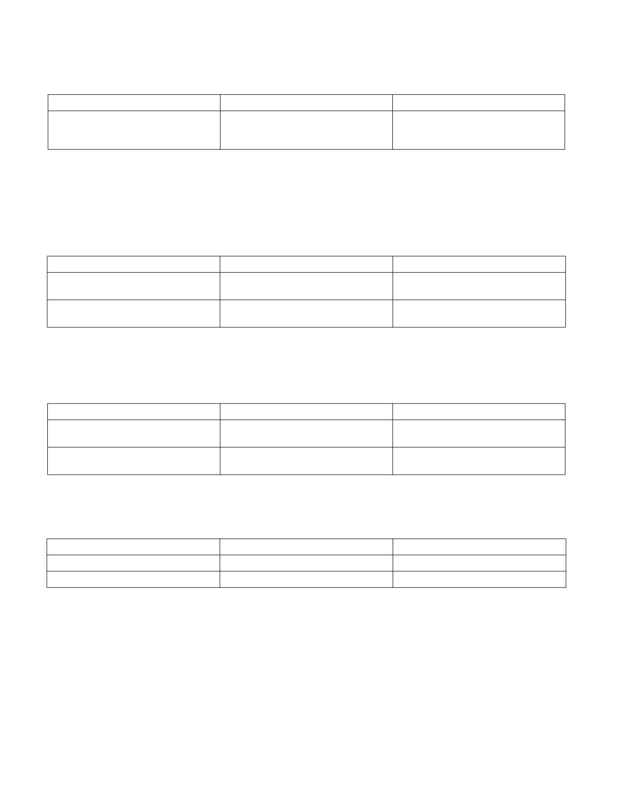
Table D-1. ADDPS, ADDSS, SUBPS, SUBSS, MULPS, MULSS, DIVPS, DIVSS, ADDPD, ADDSD, SUBPD, SUBSD, MULPD,
MULSD, DIVPD, DIVSD, ADDSUBPS, ADDSUBPD, HADDPS, HADDPD, HSUBPS, and HSUBPD (Contd.)
Source Operands
Masked Result
Unmasked Result
Neither source operand is SNaN,
Single precision or double precision QNaN
None
but #I is signaled (e.g., for Inf - Inf,
Indefinite
Inf ∗ 0, Inf / Inf, 0/0)
NOTES:
1. For Tables E-1 to E-12: op denotes the operation to be performed.
2. SNaN | 00400000H is a quiet NaN in single precision format (if SNaN is in single precision) and SNaN | 0008000000000000H is a
quiet NaN in double precision format (if SNaN is in double precision), obtained from the signaling NaN given as input.
3. Operations involving only quiet NaNs do not raise floating-point exceptions.
Table D-2. CMPPS.EQ, CMPSS.EQ, CMPPS.ORD, CMPSS.ORD,
CMPPD.EQ, CMPSD.EQ, CMPPD.ORD, and CMPSD.ORD
Source Operands
Masked Result
Unmasked Result
NaN op Opd2 (any Opd2)
00000000H or 0000000000000000H1
00000000H or 0000000000000000H1
(not an exception)
Opd1 op NaN (any Opd1)
00000000H or 0000000000000000H1
00000000H or 0000000000000000H1
(not an exception)
NOTE:
1. 32-bit results are for single, and 64-bit results for double precision operations.
Table D-3. CMPPS.NEQ, CMPSS.NEQ, CMPPS.UNORD, CMPSS.UNORD, CMPPD.NEQ, CMPSD.NEQ,
CMPPD.UNORD, and CMPSD.UNORD
Source Operands
Masked Result
Unmasked Result
NaN op Opd2 (any Opd2)
FFFFFFFFH or FFFFFFFFFFFFFFFFH1
FFFFFFFFH or FFFFFFFFFFFFFFFFH1 (not
an exception)
Opd1 op NaN (any Opd1)
FFFFFFFFH or FFFFFFFFFFFFFFFFH1
FFFFFFFFH or FFFFFFFFFFFFFFFFH1 (not
an exception)
NOTE:
1. 32-bit results are for single, and 64-bit results for double precision operations.
Table D-4. CMPPS.LT, CMPSS.LT, CMPPS.LE, CMPSS.LE, CMPPD.LT, CMPSD.LT, CMPPD.LE, and CMPSD.LE
Source Operands
Masked Result
Unmasked Result
NaN op Opd2 (any Opd2)
00000000H or 0000000000000000H1
None
Opd1 op NaN (any Opd1)
00000000H or 0000000000000000H1
None
NOTE:
1.32-bit results are for single, and 64-bit results for double precision operations.
D-6
Vol. 1

GUIDELINES FOR WRITING SIMD FLOATING-POINT EXCEPTION HANDLERS
Table D-5. CMPPS.NLT, CMPSS.NLT, CMPPS.NLE, CMPSS.NLE, CMPPD.NLT, CMPSD.NLT, CMPPD.NLE, and CMPSD.NLE
Source Operands
Masked Result
Unmasked Result
NaN op Opd2 (any Opd2)
FFFFFFFFH or FFFFFFFFFFFFFFFFH1
None
Opd1 op NaN (any Opd1)
FFFFFFFFH or FFFFFFFFFFFFFFFFH1
None
NOTE:
1. 32-bit results are for single, and 64-bit results for double precision operations.
Table D-6. COMISS and COMISD
Source Operands
Masked Result
Unmasked Result
SNaN op Opd2 (any Opd2)
OF, SF, AF = 000
None
ZF, PF, CF = 111
Opd1 op SNaN (any Opd1)
OF, SF, AF = 000
None
ZF, PF, CF = 111
QNaN op Opd2 (any Opd2)
OF, SF, AF = 000
None
ZF, PF, CF = 111
Opd1 op QNaN (any Opd1)
OF, SF, AF = 000
None
ZF, PF, CF = 111
Table D-7. UCOMISS and UCOMISD
Source Operands
Masked Result
Unmasked Result
SNaN op Opd2 (any Opd2)
OF, SF, AF = 000
None
ZF, PF, CF = 111
Opd1 op SNaN (any Opd1)
OF, SF, AF = 000
None
ZF, PF, CF = 111
QNaN op Opd2
OF, SF, AF = 000
OF, SF, AF = 000
(any Opd2 ≠ SNaN)
ZF, PF, CF = 111
ZF, PF, CF = 111 (not an exception)
Opd1 op QNaN
OF, SF, AF = 000
OF, SF, AF = 000
(any Opd1 ≠ SNaN)
ZF, PF, CF = 111
ZF, PF, CF = 111 (not an exception)
Table D-8. CVTPS2PI, CVTSS2SI, CVTTPS2PI, CVTTSS2SI, CVTPD2PI, CVTSD2SI, CVTTPD2PI, CVTTSD2SI,
CVTPS2DQ, CVTTPS2DQ, CVTPD2DQ, and CVTTPD2DQ
Source Operand
Masked Result
Unmasked Result
SNaN
80000000H or 80000000000000001
None
(Integer Indefinite)
QNaN
80000000H or 80000000000000001
None
(Integer Indefinite)
NOTE:
1.32-bit results are for single, and 64-bit results for double precision operations.
Vol. 1
D-7

GUIDELINES FOR WRITING SIMD FLOATING-POINT EXCEPTION HANDLERS
Table D-9. MAXPS, MAXSS, MINPS, MINSS, MAXPD, MAXSD, MINPD, and MINSD
Source Operands
Masked Result
Unmasked Result
Opd1 op NaN2 (any Opd1)
NaN2
None
NaN1 op Opd2 (any Opd2)
Opd2
None
NOTE:
1. SNaN and QNaN operands raise an Invalid Operation fault.
Table D-10. SQRTPS, SQRTSS, SQRTPD, and SQRTSD
Source Operand
Masked Result
Unmasked Result
QNaN
QNaN
QNaN (not an exception)
SNaN
SNaN | 00400000H or
None
SNaN | 0008000000000000H1
Source operand is not SNaN;
Single precision or
None
but #I is signaled (e.g., for
double precision QNaN Indefinite
sqrt (-1.0))
NOTE:
1. SNaN | 00400000H is a quiet NaN in single precision format (if SNaN is in single precision) and SNaN | 0008000000000000H is a
quiet NaN in double precision format (if SNaN is in double precision), obtained from the signaling NaN given as input.
Table D-11. CVTPS2PD and CVTSS2SD
Source Operands
Masked Result
Unmasked Result
QNaN
QNaN11
QNaN11 (not an exception)
SNaN
QNaN12
None
NOTES:
1. The double precision output QNaN1 is created from the single precision input QNaN as follows: the sign bit is preserved, the 8-bit
exponent FFH is replaced by the 11-bit exponent 7FFH, and the 24-bit significand is extended to a 53-bit significand by appending
29 bits equal to 0.
2. The double precision output QNaN1 is created from the single precision input SNaN as follows: the sign bit is preserved, the 8-bit
exponent FFH is replaced by the 11-bit exponent 7FFH, and the 24-bit significand is extended to a 53-bit significand by pending
29 bits equal to 0. The second most significant bit of the significand is changed from 0 to 1 to convert the signaling NaN into a
quiet NaN.
Table D-12. CVTPD2PS and CVTSD2SS
Source Operands
Masked Result
Unmasked Result
QNaN
QNaN11
QNaN11 (not an exception)
SNaN
QNaN12
None
NOTES:
1. The single precision output QNaN1 is created from the double precision input QNaN as follows: the sign bit is preserved, the 11-bit
exponent 7FFH is replaced by the 8-bit exponent FFH, and the 53-bit significand is truncated to a 24-bit significand by removing its
29 least significant bits.
2. The single precision output QNaN1 is created from the double precision input SNaN as follows: the sign bit is preserved, the 11-bit
exponent 7FFH is replaced by the 8-bit exponent FFH, and the 53-bit significand is truncated to a 24-bit significand by removing its
29 least significant bits. The second most significant bit of the significand is changed from 0 to 1 to convert the signaling NaN into
a quiet NaN.
D-8
Vol. 1

GUIDELINES FOR WRITING SIMD FLOATING-POINT EXCEPTION HANDLERS
D.4.2.3
Condition Codes, Exception Flags, and Response for Masked and Unmasked Numeric
Exceptions
In the following, the masked response is what the processor provides when a masked exception is raised by an
Intel SSE, SSE2, or SSE3 numeric instruction. The same response is provided by the floating-point emulator for
Intel SSE, SSE2, and SSE3 numeric instructions, when certain components of the quadruple input operands
generate exceptions that are masked (the emulator also generates the correct answer, as specified by IEEE Stan-
dard 754 wherever applicable, in the case when no floating-point exception occurs). The unmasked response is
what the emulator provides to the user handler for those components of the packed operands of Intel SSE, SSE2,
and SSE3 instructions that raise unmasked exceptions. Note that for pre-computation exceptions (floating-point
faults), no result is provided to the user handler. For post-computation exceptions (floating-point traps), a result is
provided to the user handler, as specified below.
In the following tables, the result is denoted by 'res', with the understanding that for the actual instruction, the
destination coincides with the first source operand (except for COMISS, UCOMISS, COMISD, and UCOMISD, whose
destination is the EFLAGS register).
Table D-13. #I - Invalid Operations
Unmasked Response
Instruction
Condition
Masked Response
and Exception Code
ADDPS
src1 or src21 = SNaN
Refer to Table D-1 for
ADDPD
NaN operands, #IA = 1
ADDSS
ADDSD
HADDPS
src1, src2 unchanged; #IA
HADDPD
= 1
ADDSUBPS (the
src1 = +Inf, src2 = -Inf or
res1 = QNaN Indefinite,
addition component)
src1 = -Inf, src2 = +Inf
#IA = 1
ADDSUBPD (the
addition component)
SUBPS
src1 or src2 = SNaN
Refer to Table D-1 for NaN
SUBPD
operands, #IA = 1
SUBSS
SUBSD
HSUBPS
HSUBPD
src1, src2 unchanged; #IA
= 1
ADDSUBPS (the
src1 = +Inf, src2 = +Inf or
res = QNaN Indefinite,
subtraction
src1 = -Inf, src2 = -Inf
#IA = 1
component)
ADDSUBPD (the
subtraction
component)
MULPS
src1 or src2 = SNaN
Refer to Table D-1 for
MULPD
NaN operands, #IA = 1
src1, src2 unchanged;
#IA = 1
MULSS
src1 = ±Inf, src2 = ±0 or
res = QNaN Indefinite,
MULSD
src1 = ±0, src2 = ±Inf
#IA = 1
DIVPS
src1 or src2 = SNaN
Refer to Table D-1 for
DIVPD
NaN operands, #IA = 1
src1, src2 unchanged;
#IA = 1
DIVSS
src1 = ±Inf, src2 = ±Inf or
res = QNaN Indefinite,
DIVSD
src1 = ±0, src2 = ±0
#IA = 1
SQRTPS
src = SNaN
Refer to Table D-10 for
src unchanged,
SQRTPD
NaN operands, #IA = 1
#IA = 1
SQRTSS
src < 0
res = QNaN Indefinite,
SQRTSD
(note that -0 < 0 is false)
#IA = 1
Vol. 1
D-9

GUIDELINES FOR WRITING SIMD FLOATING-POINT EXCEPTION HANDLERS
Table D-13. #I - Invalid Operations (Contd.)
Unmasked Response
Instruction
Condition
Masked Response
and Exception Code
MAXPS
src1 = NaN or src2 = NaN
res = src2, #IA = 1
src1, src2 unchanged; #IA
MAXSS
= 1
MAXPD
MAXSD
MINPS
src1 = NaN or src2 = NaN
res = src2, #IA = 1
src1, src2 unchanged; #IA
MINSS
= 1
MINPD
MINSD
CMPPS.LT
src1 = NaN or src2 = NaN
Refer to Table D-4 and Table D-5 for
src1, src2 unchanged; #IA
CMPPS.LE
NaN operands; #IA = 1
= 1
CMPPS.NLT
CMPPS.NLE
CMPSS.LT
CMPSS.LE
CMPSS.NLT
CMPSS.NLE
CMPPD.LT
CMPPD.LE
CMPPD.NLT
CMPPD.NLE
CMPSD.LT
CMPSD.LE
CMPSD.NLT
CMPSD.NLE
COMISS
src1 = NaN or src2 = NaN
Refer to Table D-6 for NaN
src1, src2, EFLAGS
COMISD
operands
unchanged; #IA = 1
UCOMISS
src1 = SNaN or src2 = SNaN
Refer to Table D-7 for NaN
src1, src2, EFLAGS
UCOMISD
operands
unchanged; #IA = 1
CVTPS2PI
src = NaN, ±Inf, or
res = Integer Indefinite,
src unchanged,
CVTSS2SI
|(src)rnd | > 7FFFFFFFH and (src)rnd ≠
#IA = 1
#IA = 1
CVTPD2PI
80000000H
CVTSD2SI
CVTPS2DQ
See Note2 for information
CVTPD2DQ
on rnd.
CVTTPS2PI
src = NaN, ±Inf, or
res = Integer Indefinite,
src unchanged,
CVTTSS2SI
|(src)rz | > 7FFFFFFFH and (src)rz ≠
#IA = 1
#IA = 1
CVTTPD2PI
80000000H
CVTTSD2SI
CVTTPS2DQ
See Note2 for information
CVTTPD2DQ
on rz.
D-10
Vol. 1

GUIDELINES FOR WRITING SIMD FLOATING-POINT EXCEPTION HANDLERS
Table D-13. #I - Invalid Operations (Contd.)
Unmasked Response
Instruction
Condition
Masked Response
and Exception Code
CVTPS2PD
src = SNAN
Refer to Table D-11 for
src unchanged,
CVTSS2SD
NaN operands
#IA = 1
CVTPD2PS
src = SNAN
Refer to Table D-12 for
src unchanged,
CVTSD2SS
NaN operands
#IA = 1
NOTES:
1. For Tables E-13 to E-18:
- src denotes the single source operand of a unary operation.
- src1, src2 denote the first and second source operand of a binary operation.
- res denotes the numerical result of an operation.
2. rnd signifies the user rounding mode from MXCSR, and rz signifies the rounding mode toward zero. (truncate), when rounding a
floating-point value to an integer. For more information, refer to Table 4-9.
3. For NAN encodings, see Table 4-3.
Table D-14. #Z - Divide-by-Zero
Unmasked Response
Instruction
Condition
Masked Response
and Exception Code
DIVPS
src1 = finite non-zero (normal, or
res = ±Inf,
src1, src2 unchanged;
DIVSS
denormal)
#ZE = 1
#ZE = 1
DIVPD
src2 = ±0
DIVPS
Vol. 1
D-11

GUIDELINES FOR WRITING SIMD FLOATING-POINT EXCEPTION HANDLERS
Table D-15. #D - Denormal Operand
Unmasked Response and
Instruction
Condition
Masked Response
Exception Code
ADDPS
src1 = denormal1 or
res = Result rounded to the
src1, src2 unchanged;
ADDPD
src2 = denormal (and
destination precision and using the
#DE = 1
ADDSUBPS
the DAZ bit in MXCSR
bounded exponent, but only if no
ADDSUBPD
is 0)
unmasked post-computation
Note that SQRT, CVTPS2PD,
HADDPS
exception occurs;
CVTSS2SD, CVTPD2PS, CVTSD2SS
HADDPD
#DE = 1.
have only 1 src.
SUBPS
SUBPD
HSUBPS
HSUBPD
MULPS
MULPD
DIVPS
DIVPD
SQRTPS
SQRTPD
MAXPS
MAXPD
MINPS
MINPD
ADDSS
ADDSD
SUBSS
SUBSD
MULSS
MULSD
DIVSS
DIVSD
SQRTSS
SQRTSD
MAXSS
MAXSD
MINSS
MINSD
CVTPS2PD
CVTSS2SD
CVTPD2PS
CVTSD2SS
CMPPS
src1 = denormal1 or
Comparison result, stored in the
src1, src2 unchanged;
CMPPD
src2 = denormal (and
destination register;
#DE = 1
CMPSS
the DAZ bit in MXCSR
#DE = 1
CMPSD
is 0)
COMISS
src1 = denormal1 or
Comparison result, stored in the
src1, src2 unchanged;
COMISD
src2 = denormal (and
EFLAGS register;
#DE = 1
UCOMISS
the DAZ bit in MXCSR
#DE = 1
UCOMISD
is 0)
NOTE:
1. For denormal encodings, see Section 4.8.3.2, “Normalized and Denormalized Finite Numbers.”
D-12
Vol. 1

GUIDELINES FOR WRITING SIMD FLOATING-POINT EXCEPTION HANDLERS
Table D-16. #O - Numeric Overflow
Unmasked Response and
Instruction
Condition
Masked Response
Exception Code
Rounding
Sign
Result & Status Flags
ADDPS
To
#OE = 1, #PE = 1
ADDSUBPS
nearest
+
res =
+
∞
HADDPS
-
res =
-∞
SUBPS
HSUBPS
Toward
-∞
#OE = 1, #PE = 1
res = (result calculated with
Rounded result >
MULPS
+
res = 1.11…1 * 2127
unbounded exponent and rounded
largest single
DIVPS
-
res =
-∞
to the destination precision) / 2192
precision finite
ADDSS
#OE = 1
normal value
Toward
+
∞
#OE = 1, #PE = 1
SUBSS
#PE = 1 if the result is inexact
+
res =
+
∞
MULSS
-
res = -1.11…1 * 2127
DIVSS
CVTPD2PS
Toward
#OE = 1, #PE = 1
CVTSD2SS
0
+
res = 1.11…1 * 2127
-
res = -1.11…1 * 2127
Rounding
Sign
Result & Status Flags
ADDPD
To
#OE = 1, #PE = 1
ADDSUBPD
nearest
+
res =
+
∞
HADDPD
-
res =
-∞
SUBPD
Toward
-∞
#OE = 1, #PE = 1
res = (result calculated with
HSUBPD
Rounded result >
+
res = 1.11…1 * 21023
unbounded exponent and rounded
MULPD
largest double
-
res =
-∞
to the destination precision) / 21536
DIVPD
precision finite
• #OE = 1
ADDSD
normal value
Toward
+
∞
#OE = 1, #PE = 1
• #PE = 1 if the result is inexact
SUBSD
+
res =
+
∞
MULSD
-
res = -1.11…1 * 21023
DIVSD
Toward
#OE = 1, #PE = 1
0
+
res = 1.11…1 * 21023
-
res = -1.11…1 * 21023
Vol. 1
D-13

GUIDELINES FOR WRITING SIMD FLOATING-POINT EXCEPTION HANDLERS
Table D-17. #U - Numeric Underflow
Unmasked Response and
Instruction
Condition
Masked Response
Exception Code
ADDPS
Result calculated with unbounded
res = ±0, denormal, or normal
res = (result calculated with
ADDSUBPS
exponent and rounded to the
unbounded exponent and rounded
HADDPS
destination precision < smallest
#UE = 1 and #PE = 1,
to the destination precision) * 2192
SUBPS
single precision finite normal value.
but only if the result is
• #UE = 1
HSUBPS
inexact
• #PE = 1 if the result is inexact
MULPS
DIVPS
ADDSS
SUBSS
MULSS
DIVSS
CVTPD2PS
CVTSD2SS
ADDPD
Result calculated with unbounded
res = ±0, denormal or normal
res = (result calculated with
ADDSUBPD
exponent and rounded to the
unbounded exponent and rounded
HADDPD
destination precision < smallest
#UE = 1 and #PE = 1,
to the destination precision) * 21536
SUBPD
double precision finite normal value.
but only if the result is
• #UE = 1
HSUBPD
inexact
• #PE = 1 if the result is inexact
MULPD
DIVPD
ADDSD
SUBSD
MULSD
DIVSD
D-14
Vol. 1

GUIDELINES FOR WRITING SIMD FLOATING-POINT EXCEPTION HANDLERS
Table D-18. #P - Inexact Result (Precision)
Instruction
Condition
Masked Response
Unmasked Response and Exception Code
ADDPS
The result is not exactly
res = Result rounded to the
Only if no underflow/overflow condition occurred, or
ADDPD
representable in the
destination precision and
if the corresponding exceptions are masked:
ADDSUBPS
destination format.
using the bounded
• Set #OE if masked overflow and set result as
ADDSUBPD
exponent, but only if no
described above for masked overflow.
HADDPS
unmasked underflow or
• Set #UE if masked underflow and set result as
described above for masked underflow.
HADDPD
overflow conditions occur
If neither underflow nor overflow, res equals the
SUBPS
(this exception can occur in
result rounded to the destination precision and using
SUBPD
the presence of a masked
the bounded exponent set #PE = 1.
HSUBPS
underflow or overflow); #PE
HSUBPD
= 1.
MULPS
MULPD
DIVPS
DIVPD
SQRTPS
SQRTPD
CVTDQ2PS
CVTPI2PS
CVTPS2PI
CVTPS2DQ
CVTPD2PI
CVTPD2DQ
CVTPD2PS
CVTTPS2PI
CVTTPD2PI
CVTTPD2DQ
CVTTPS2DQ
ADDSS
ADDSD
SUBSS
SUBSD
MULSS
MULSD
DIVSS
DIVSD
SQRTSS
SQRTSD
CVTSI2SS
CVTSS2SI
CVTSD2SI
CVTSD2SS
CVTTSS2SI
CVTTSD2SI
D.4.3
Example SIMD Floating-Point Emulation Implementation
The sample code listed below may be considered as being part of a user-level floating-point exception filter for the
intel SSE, SSE2, and SSE3 numeric instructions. It is assumed that the filter function is invoked by a low-level
exception handler (invoked for exception 19 when an unmasked floating-point exception occurs), and that it oper-
ates as explained in Section D.4.1, “Floating-Point Emulation.” The sample code does the emulation only for the
SSE instructions for addition, subtraction, multiplication, and division. For this, it uses C code and x87 FPU opera-
tions. Operations corresponding to other Intel SSE, SSE2, and SSE3 numeric instructions can be emulated simi-
larly. The example assumes that the emulation function receives a pointer to a data structure specifying a number
of input parameters: the operation that caused the exception, a set of sub-operands (unpacked, of type float), the
Vol. 1
D-15
GUIDELINES FOR WRITING SIMD FLOATING-POINT EXCEPTION HANDLERS
rounding mode (the precision is always single), exception masks (having the same relative bit positions as in the
MXCSR but starting from bit 0 in an unsigned integer), and flush-to-zero and denormals-are-zeros indicators.
The output parameters are a floating-point result (of type float), the cause of the exception (identified by constants
not explicitly defined below), and the exception status flags. The corresponding C definition is:
typedef struct {
unsigned int operation;
//SSE or SSE2 operation: ADDPS, ADDSS, ...
unsigned int operand1_uint32; //first operand value
unsigned int operand2_uint32; //second operand value (if any)
float result_fval; // result value (if any)
unsigned int rounding_mode; //rounding mode
unsigned int exc_masks; //exception masks, in the order P,U,O,Z,D,I
unsigned int exception_cause; //exception cause
unsigned int status_flag_inexact; //inexact status flag
unsigned int status_flag_underflow; //underflow status flag
unsigned int status_flag_overflow; //overflow status flag
unsigned int status_flag_divide_by_zero;
//divide by zero status flag
unsigned int status_flag_denormal_operand;
//denormal operand status flag
unsigned int status_flag_invalid_operation;
//invalid operation status flag
unsigned int ftz; // flush-to-zero flag
unsigned int daz; // denormals-are-zeros flag
} EXC_ENV;
The arithmetic operations exemplified are emulated as follows:
1. If the denormals-are-zeros mode is enabled (the DAZ bit in MXCSR is set to 1), replace all the denormal inputs
with zeroes of the same sign (the denormal flag is not affected by this change).
2. Perform the operation using x87 FPU instructions, with exceptions disabled, the original user rounding mode,
and single precision. This reveals invalid, denormal, or divide-by-zero exceptions (if there are any) and stores
the result in memory as a double precision value (whose exponent range is large enough to look like
“unbounded” to the result of the single precision computation).
3. If no unmasked exceptions were detected, determine if the magnitude of the result is less than the smallest
normal number that can be represented in single precision format, or greater than the largest normal number
that can be represented in single precision format (huge). If an unmasked overflow or underflow occurs,
calculate the scaled result that will be handed to the user exception handler, as specified by IEEE Standard 754.
4. If no exception was raised, calculate the result with a “bounded” exponent. If the result is tiny, it requires
denormalization (shifting the significand right while incrementing the exponent to bring it into the admissible
range of [-126,+127] for single precision floating-point numbers).
The result obtained in step 2 cannot be used because it might incur a double rounding error (it was rounded to
24 bits in step 2, and might have to be rounded again in the denormalization process). To overcome this is,
calculate the result as a double precision value, and store it to memory in single precision format.
Rounding first to 53 bits in the significand, and then to 24 never causes a double rounding error (exact
properties exist that state when double-rounding error occurs, but for the elementary arithmetic operations,
the rule of thumb is that if an infinitely precise result is rounded to 2p+1 bits and then again to p bits, the result
is the same as when rounding directly to p bits, which means that no double-rounding error occurs).
5. If the result is inexact and the inexact exceptions are unmasked, the calculated result will be delivered to the
user floating-point exception handler.
6. The flush-to-zero case is dealt with if the result is tiny.
D-16
Vol. 1
GUIDELINES FOR WRITING SIMD FLOATING-POINT EXCEPTION HANDLERS
7. The emulation function returns RAISE_EXCEPTION to the filter function if an exception has to be raised (the
exception_cause field indicates the cause). Otherwise, the emulation function returns DO_NOT_ RAISE_EX-
CEPTION. In the first case, the result is provided by the user exception handler called by the filter function. In
the second case, it is provided by the emulation function. The filter function has to collect all the partial results,
and to assemble the scalar or packed result that is used if execution is to continue.
Example D-2. SIMD Floating-Point Emulation
// masks for individual status word bits
#define PRECISION_MASK 20H
#define UNDERFLOW_MASK 10H
#define OVERFLOW_MASK 08H
#define ZERODIVIDE_MASK 04H
#define DENORMAL_MASK 02H
#define INVALID_MASK 01H
// 32-bit constants
static unsigned ZEROF_ARRAY[] = {00000000H};
#define ZEROF *(float *) ZEROF_ARRAY
// +0.0
static unsigned NZEROF_ARRAY[] = {80000000H};
#define NZEROF *(float *) NZEROF_ARRAY
// -0.0
static unsigned POSINFF_ARRAY[] = {7f800000H};
#define POSINFF *(float *)POSINFF_ARRAY
// +Inf
static unsigned NEGINFF_ARRAY[] = {ff800000H};
#define NEGINFF *(float *)NEGINFF_ARRAY
// -Inf
// 64-bit constants
static unsigned MIN_SINGLE_NORMAL_ARRAY [] = {00000000H, 38100000H};
#define MIN_SINGLE_NORMAL *(double *)MIN_SINGLE_NORMAL_ARRAY
// +1.0 * 2^-126
static unsigned MAX_SINGLE_NORMAL_ARRAY [] = {70000000H, 47efffffH};
#define MAX_SINGLE_NORMAL *(double *)MAX_SINGLE_NORMAL_ARRAY
// +1.1...1*2^127
static unsigned TWO_TO_192_ARRAY[] = {00000000H, 4bf00000H};
#define TWO_TO_192 *(double *)TWO_TO_192_ARRAY
// +1.0 * 2^192
static unsigned TWO_TO_M192_ARRAY[] = {00000000H, 33f00000H};
#define TWO_TO_M192 *(double *)TWO_TO_M192_ARRAY
// +1.0 * 2^-192
// auxiliary functions
static int isnanf (unsigned int ); // returns 1 if f is a NaN, and 0 otherwise
static float quietf (unsigned int ); // converts a signaling NaN to a quiet
// NaN, and leaves a quiet NaN unchanged
static unsigned int check_for_daz (unsigned int ); // converts denormals
// to zeros of the same sign;
// does not affect any status flags
// emulation of SSE and SSE2 instructions using
// C code and x87 FPU instructions
unsigned int
simd_fp_emulate (EXC_ENV *exc_env)
{
int uiopd1; // first operand of the add, subtract, multiply, or divide
int uiopd2; // second operand of the add, subtract, multiply, or divide
float res; // result of the add, subtract, multiply, or divide
double dbl_res24; // result with 24-bit significand, but "unbounded" exponent
Vol. 1
D-17
GUIDELINES FOR WRITING SIMD FLOATING-POINT EXCEPTION HANDLERS
// (needed to check tininess, to provide a scaled result to
// an underflow/overflow trap handler, and in flush-to-zero mode)
double dbl_res;
// result in double precision format (needed to avoid a
// double rounding error when denormalizing)
unsigned int result_tiny;
unsigned int result_huge;
unsigned short int sw; // 16 bits
unsigned short int cw; // 16 bits
// have to check first for faults (V, D, Z), and then for traps (O, U, I)
// initialize x87 FPU (floating-point exceptions are masked)
_asm {
fninit;
}
result_tiny = 0;
result_huge = 0;
switch (exc_env->operation) {
case ADDPS:
case ADDSS:
case SUBPS:
case SUBSS:
case MULPS:
case MULSS:
case DIVPS:
case DIVSS:
uiopd1 = exc_env->operand1_uint32; // copy as unsigned int
// do not copy as float to avoid conversion
// of SNaN to QNaN by compiled code
uiopd2 = exc_env->operand2_uint32;
// do not copy as float to avoid conversion of SNaN
// to QNaN by compiled code
uiopd1 = check_for_daz (uiopd1); // operand1 = +0.0 * operand1 if it is
// denormal and DAZ=1
uiopd2 = check_for_daz (uiopd2); // operand2 = +0.0 * operand2 if it is
// denormal and DAZ=1
// execute the operation and check whether the invalid, denormal, or
// divide by zero flags are set and the respective exceptions enabled
// set control word with rounding mode set to exc_env->rounding_mode,
// single precision, and all exceptions disabled
switch (exc_env->rounding_mode) {
case ROUND_TO_NEAREST:
cw = 003fH; // round to nearest, single precision, exceptions masked
break;
case ROUND_DOWN:
cw = 043fH; // round down, single precision, exceptions masked
break;
case ROUND_UP:
cw = 083fH; // round up, single precision, exceptions masked
break;
case ROUND_TO_ZERO:
cw = 0c3fH; // round to zero, single precision, exceptions masked
break;
default:
;
}
__asm {
fldcw WORD PTR cw;
D-18
Vol. 1
GUIDELINES FOR WRITING SIMD FLOATING-POINT EXCEPTION HANDLERS
}
// compute result and round to the destination precision, with
// "unbounded" exponent (first IEEE rounding)
switch (exc_env->operation) {
case ADDPS:
case ADDSS:
// perform the addition
__asm {
fnclex;
// load input operands
fld DWORD PTR uiopd1; // may set denormal or invalid status flags
fld DWORD PTR uiopd2; // may set denormal or invalid status flags
faddp st(1), st(0); // may set inexact or invalid status flags
// store result
fstp QWORD PTR dbl_res24; // exact
}
break;
case SUBPS:
case SUBSS:
// perform the subtraction
__asm {
fnclex;
// load input operands
fld DWORD PTR uiopd1; // may set denormal or invalid status flags
fld DWORD PTR uiopd2; // may set denormal or invalid status flags
fsubp st(1), st(0); // may set the inexact or invalid status flags
// store result
fstp QWORD PTR dbl_res24; // exact
}
break;
case MULPS:
case MULSS:
// perform the multiplication
__asm {
fnclex;
// load input operands
fld DWORD PTR uiopd1; // may set denormal or invalid status flags
fld DWORD PTR uiopd2; // may set denormal or invalid status flags
fmulp st(1), st(0); // may set inexact or invalid status flags
// store result
fstp QWORD PTR dbl_res24; // exact
}
break;
case DIVPS:
case DIVSS:
// perform the division
__asm {
fnclex;
// load input operands
fld DWORD PTR uiopd1; // may set denormal or invalid status flags
fld DWORD PTR uiopd2; // may set denormal or invalid status flags
fdivp st(1), st(0); // may set the inexact, divide by zero, or
// invalid status flags
// store result
fstp QWORD PTR dbl_res24; // exact
}
break;
Vol. 1
D-19
GUIDELINES FOR WRITING SIMD FLOATING-POINT EXCEPTION HANDLERS
default:
; // will never occur
}
// read status word
__asm {
fstsw WORD PTR sw;
}
if (sw & ZERODIVIDE_MASK)
sw = sw & ~DENORMAL_MASK; // clear D flag for (denormal / 0)
// if invalid flag is set, and invalid exceptions are enabled, take trap
if (!(exc_env->exc_masks & INVALID_MASK) && (sw & INVALID_MASK)) {
exc_env->status_flag_invalid_operation = 1;
exc_env->exception_cause = INVALID_OPERATION;
return (RAISE_EXCEPTION);
}
// checking for NaN operands has priority over denormal exceptions;
// also fix for the SSE and SSE2
// differences in treating two NaN inputs between the
// instructions and other IA-32 instructions
if (isnanf (uiopd1) || isnanf (uiopd2)) {
if (isnanf (uiopd1) && isnanf (uiopd2))
exc_env->result_fval = quietf (uiopd1);
else
exc_env->result_fval = (float)dbl_res24; // exact
if (sw & INVALID_MASK) exc_env->status_flag_invalid_operation = 1;
return (DO_NOT_RAISE_EXCEPTION);
}
// if denormal flag set, and denormal exceptions are enabled, take trap
if (!(exc_env->exc_masks & DENORMAL_MASK) && (sw & DENORMAL_MASK)) {
exc_env->status_flag_denormal_operand = 1;
exc_env->exception_cause = DENORMAL_OPERAND;
return (RAISE_EXCEPTION);
}
// if divide by zero flag set, and divide by zero exceptions are
// enabled, take trap (for divide only)
if (!(exc_env->exc_masks & ZERODIVIDE_MASK) && (sw & ZERODIVIDE_MASK)) {
exc_env->status_flag_divide_by_zero = 1;
exc_env->exception_cause = DIVIDE_BY_ZERO;
return (RAISE_EXCEPTION);
}
// done if the result is a NaN (QNaN Indefinite)
res = (float)dbl_res24;
if (isnanf (*(unsigned int *)&res)) {
exc_env->result_fval = res; // exact
exc_env->status_flag_invalid_operation = 1;
return (DO_NOT_RAISE_EXCEPTION);
}
// dbl_res24 is not a NaN at this point
if (sw & DENORMAL_MASK) exc_env->status_flag_denormal_operand = 1;
// Note: (dbl_res24 == 0.0 && sw & PRECISION_MASK) cannot occur
if (-MIN_SINGLE_NORMAL < dbl_res24 && dbl_res24 < 0.0 ||
0.0 < dbl_res24 && dbl_res24 < MIN_SINGLE_NORMAL) {
D-20
Vol. 1
GUIDELINES FOR WRITING SIMD FLOATING-POINT EXCEPTION HANDLERS
result_tiny = 1;
}
// check if the result is huge
if (NEGINFF < dbl_res24 && dbl_res24 < -MAX_SINGLE_NORMAL ||
MAX_SINGLE_NORMAL < dbl_res24 && dbl_res24 < POSINFF) {
result_huge = 1;
}
// at this point, there are no enabled I,D, or Z exceptions
// to take; the instr.
// might lead to an enabled underflow, enabled underflow and inexact,
// enabled overflow, enabled overflow and inexact, enabled inexact, or
// none of these; if there are no U or O enabled exceptions, re-execute
// the instruction using IA-32 double precision format, and the
// user's rounding mode; exceptions must have
// been disabled before calling
// this function; an inexact exception may be reported on the 53-bit
// fsubp, fmulp, or on both the 53-bit and 24-bit conversions, while an
// overflow or underflow (with traps disabled) may be reported on the
// conversion from dbl_res to res
// check whether there is an underflow, overflow,
// or inexact trap to be taken
// if the underflow traps are enabled and the result is
// tiny, take underflow trap
if (!(exc_env->exc_masks & UNDERFLOW_MASK) && result_tiny) {
dbl_res24 = TWO_TO_192 * dbl_res24; // exact
exc_env->status_flag_underflow = 1;
exc_env->exception_cause = UNDERFLOW;
exc_env->result_fval = (float)dbl_res24; // exact
if (sw & PRECISION_MASK) exc_env->status_flag_inexact = 1;
return (RAISE_EXCEPTION);
}
// if overflow traps are enabled and the result is huge, take
// overflow trap
if (!(exc_env->exc_masks & OVERFLOW_MASK) && result_huge) {
dbl_res24 = TWO_TO_M192 * dbl_res24; // exact
exc_env->status_flag_overflow = 1;
exc_env->exception_cause = OVERFLOW;
exc_env->result_fval = (float)dbl_res24; // exact
if (sw & PRECISION_MASK) exc_env->status_flag_inexact = 1;
return (RAISE_EXCEPTION);
}
// set control word with rounding mode set to exc_env->rounding_mode,
// double precision, and all exceptions disabled
cw = cw | 0200H; // set precision to double
__asm {
fldcw WORD PTR cw;
}
switch (exc_env->operation) {
case ADDPS:
case ADDSS:
// perform the addition
__asm {
// load input operands
fld DWORD PTR uiopd1; // may set the denormal status flag
fld DWORD PTR uiopd2; // may set the denormal status flag
faddp st(1), st(0); // rounded to 53 bits, may set the inexact
// status flag
Vol. 1
D-21
GUIDELINES FOR WRITING SIMD FLOATING-POINT EXCEPTION HANDLERS
// store result
fstp QWORD PTR dbl_res; // exact, will not set any flag
}
break;
case SUBPS:
case SUBSS:
// perform the subtraction
__asm {
// load input operands
fld DWORD PTR uiopd1; // may set the denormal status flag
fld DWORD PTR uiopd2; // may set the denormal status flag
fsubp st(1), st(0);
// rounded to 53 bits, may set the inexact
// status flag
// store result
fstp QWORD PTR dbl_res; // exact, will not set any flag
}
break;
case MULPS:
case MULSS:
// perform the multiplication
__asm {
// load input operands
fld DWORD PTR uiopd1; // may set the denormal status flag
fld DWORD PTR uiopd2; // may set the denormal status flag
fmulp st(1), st(0);
// rounded to 53 bits, exact
// store result
fstp QWORD PTR dbl_res; // exact, will not set any flag
}
break;
case DIVPS:
case DIVSS:
// perform the division
__asm {
// load input operands
fld DWORD PTR uiopd1; // may set the denormal status flag
fld DWORD PTR uiopd2; // may set the denormal status flag
fdivp st(1), st(0);
// rounded to 53 bits, may set the inexact
// status flag
// store result
fstp QWORD PTR dbl_res; // exact, will not set any flag
}
break;
default:
; // will never occur
}
// calculate result for the case an inexact trap has to be taken, or
// when no trap occurs (second IEEE rounding)
res = (float)dbl_res;
// may set P, U or O; may also involve denormalizing the result
// read status word
__asm {
fstsw WORD PTR sw;
}
// if inexact traps are enabled and result is inexact, take inexact trap
if (!(exc_env->exc_masks & PRECISION_MASK) &&
((sw & PRECISION_MASK) || (exc_env->ftz && result_tiny))) {
exc_env->status_flag_inexact = 1;
D-22
Vol. 1
GUIDELINES FOR WRITING SIMD FLOATING-POINT EXCEPTION HANDLERS
exc_env->exception_cause = INEXACT;
if (result_tiny) {
exc_env->status_flag_underflow = 1;
// if ftz = 1 and result is tiny, result = 0.0
// (no need to check for underflow traps disabled: result tiny and
// underflow traps enabled would have caused taking an underflow
// trap above)
if (exc_env->ftz) {
if (res > 0.0)
res = ZEROF;
else if (res < 0.0)
res = NZEROF;
// else leave res unchanged
}
}
if (result_huge) exc_env->status_flag_overflow = 1;
exc_env->result_fval = res;
return (RAISE_EXCEPTION);
}
// if it got here, then there is no trap to be taken; the following must
// hold: ((the MXCSR U exceptions are disabled or
//
// the MXCSR underflow exceptions are enabled and the underflow flag is
// clear and (the inexact flag is set or the inexact flag is clear and
// the 24-bit result with unbounded exponent is not tiny)))
// and (the MXCSR overflow traps are disabled or the overflow flag is
// clear) and (the MXCSR inexact traps are disabled or the inexact flag
// is clear)
//
// in this case, the result has to be delivered (the status flags are
// sticky, so they are all set correctly already)
// read status word to see if result is inexact
__asm {
fstsw WORD PTR sw;
}
if (sw & UNDERFLOW_MASK) exc_env->status_flag_underflow = 1;
if (sw & OVERFLOW_MASK) exc_env->status_flag_overflow = 1;
if (sw & PRECISION_MASK) exc_env->status_flag_inexact = 1;
// if ftz = 1, and result is tiny (underflow traps must be disabled),
// result = 0.0
if (exc_env->ftz && result_tiny) {
if (res > 0.0)
res = ZEROF;
else if (res < 0.0)
res = NZEROF;
// else leave res unchanged
exc_env->status_flag_inexact = 1;
exc_env->status_flag_underflow = 1;
}
exc_env->result_fval = res;
if (sw & ZERODIVIDE_MASK) exc_env->status_flag_divide_by_zero = 1;
if (sw & DENORMAL_MASK) exc_env->status_flag_denormal= 1;
if (sw & INVALID_MASK) exc_env->status_flag_invalid_operation = 1;
return (DO_NOT_RAISE_EXCEPTION);
break;
case CMPPS:
Vol. 1
D-23
GUIDELINES FOR WRITING SIMD FLOATING-POINT EXCEPTION HANDLERS
case CMPSS:
break;
case COMISS:
case UCOMISS:
break;
case CVTPI2PS:
case CVTSI2SS:
break;
case CVTPS2PI:
case CVTSS2SI:
case CVTTPS2PI:
case CVTTSS2SI:
break;
case MAXPS:
case MAXSS:
case MINPS:
case MINSS:
break;
case SQRTPS:
case SQRTSS:
break;
case UNSPEC:
break;
default:
}
}
D-24
Vol. 1
APPENDIX E
INTEL® MEMORY PROTECTION EXTENSIONS
NOTE
Intel® MPX has been deprecated and will not be available on any future processors.
E.1
INTEL® MEMORY PROTECTION EXTENSIONS (INTEL® MPX)
Intel® Memory Protection Extensions (Intel® MPX) is a new capability introduced into Intel Architecture. Intel
MPX can increase the robustness of software when it is used in conjunction with compiler changes to check mem-
ory references, for those references whose compile-time normal intentions are usurped at runtime due to buffer
overflow or underflow. Two of the most important goals of Intel MPX are to provide this capability at low perfor-
mance overhead for newly compiled code, and to provide compatibility mechanisms with legacy software com-
ponents. A direct benefit Intel MPX provides is hardening software against malicious attacks designed to cause
or exploit buffer overruns. This chapter describes the software visible interfaces of this extension.
E.2
INTRODUCTION
Intel MPX is designed to allow a system (i.e., the logical processor(s) and the OS software) to run both Intel MPX
enabled software and legacy software (written for processors without Intel MPX). When executing software
containing a mixture of Intel MPX-unaware code (legacy code) and Intel MPX-enabled code, the legacy code does
not benefit from Intel MPX, but it also does not experience any change in functionality or reduction in performance.
The performance of Intel MPX-enabled code running on processors that do not support Intel MPX may be similar to
the use of embedding NOPs in the instruction stream.
Intel MPX is designed such that an Intel MPX enabled application can link with, call into, or be called from legacy
software (libraries, etc.) while maintaining existing application binary interfaces (ABIs). And in most cases, the
benefit of Intel MPX requires minimal changes to the source code at the application programming interfaces (APIs)
to legacy library/applications. As described later, Intel MPX associates bounds with pointers in a novel manner,
and the Intel MPX hardware uses bounds to check that the pointer based accesses are suitably constrained. Intel
MPX enabled software is not required to uniformly or universally utilize the new hardware capabilities over all
memory references. Specifically, programmers can selectively use Intel MPX to protect a subset of pointers.
The code enabled for Intel MPX benefits from memory protection against vulnerability such as buffer overrun.
Therefore there is a heightened incentive for software vendors to adopt this technology. At the same time, the
security benefit of Intel MPX-protection can be implemented according to the business priorities of software
vendors. A software vendor can choose to adopt Intel MPX in some modules to realize partial benefit from Intel MPX
quickly, and introduce Intel MPX in other modules in phases (e.g., some programmer intervention might be
required at the interface to legacy calls). This adaptive property of Intel MPX is designed to give software vendors
control on their schedule and modularity of adoption. It also allows a software vendor to secure defense for higher
priority or more attack-prone software first; and allows the use of Intel MPX features in one phase of software engi-
neering (e.g., testing) and not in another (e.g., general release) as dictated by business realities.
The initial goal of Intel MPX is twofold: (1) provide means to defend a system against attacks that originate
external to some trust perimeter where the trust perimeter subsumes the system memory and integral data repos-
itories, and (2) provide means to pinpoint accidental logic defects in pointer usage, by undergirding memory refer-
ences with hardware based pointer validation.
As with any instruction set extensions, Intel MPX can be used by application developers beyond detecting buffer
overflow, the processor does not limit the use of Intel MPX for buffer overflow detection.
Vol. 1
E-1
INTEL® MEMORY PROTECTION EXTENSIONS
E.3
INTEL MPX PROGRAMMING ENVIRONMENT
Intel MPX introduces new bounds registers and new instructions that operate on bounds registers. Intel MPX
allows an OS to support user mode software (operating at CPL=3) and supervisor mode software (CPL < 3) to add
memory protection capability against buffer overrun. It provides controls to enable Intel MPX extensions for user
mode and supervisor mode independently. Intel MPX extensions are designed to allow software to associate
bounds with pointers, and allow software to check memory references against the bounds associated with the
pointer to prevent out of bound memory access (thus preventing buffer overflow).The bounds registers hold lower
bound and upper bound that can be checked when referencing memory. An out-of-bounds memory reference then
causes a #BR exception. Intel MPX also introduces configuration facilities that the OS must manage to support
enabling of user-mode (and/or supervisor-mode) software operations using bounds registers.
E.3.1
Detection and Enumeration of Intel MPX Interfaces
Detection of hardware support for processor extended state component is provided by the main CPUID.0DH.00H.
Specifically, the return value in EDX:EAX of CPUID.0DH.00H provides a 64-bit wide bit vector of hardware support
of processor state components.
If CPUID.07H.00H:EBX.MPX[14] = 1 (the processor supports Intel MPX), CPUID.0DH.00H:EAX[4:3] will
enumerate the XSAVE state components associated with Intel MPX. These two component states of Intel MPX are
the following:
• BNDREGS: CPUID.0DH.00H:EAX[3] indicates XCR0.BNDREGS[bit 3] is supported. This bit indicates bound
register component of Intel MPX state, comprised of four bounds registers, BND0-BND3 (see Appendix E.3.2).
• BNDCSR: CPUID.0DH.00H:EAX[4] indicates XCR0.BNDCSR[bit 4] is supported. This bit indicates bounds
configuration and status component of Intel MPX comprised of BNDCFGU and BNDSTATUS. OS must enable
both BNDCSR and BNDREGS bits in XCR0 to ensure full Intel MPX support to applications.
• The size of the processor state component, enabled by XCR0.BNDREGS, is enumerated by
CPUID.0DH.03H:EAX[31:0] and the byte offset of this component relative to the beginning of the
XSAVE/XRSTOR area is reported by CPUID.0DH.03H:EBX[31:0].
• The size of the processor state component, enabled by XCR0.BNDCSR, is enumerated by
CPUID.0DH.04H:EAX[31:0] and the byte offset of this component relative to the beginning of the
XSAVE/XRSTOR area is reported by CPUID.0DH.04H:EBX[31:0].
On processors that support Intel MPX, CPUID.0DH.00H:EAX[3] and CPUID.0DH.00H:EAX[4] will both be 1. On
processors that do not support Intel MPX, CPUID.0DH.00H:EAX[3] and CPUID.0DH.00H:EAX[4] will both be 0.
The layout of XCR0 for extended processor state components defined in Intel Architecture is shown in Figure 2-8 of
the Intel® 64 and IA-32 Architectures Software Developer’s Manual, Volume 3A.
Enabling Intel MPX requires an OS to manage bits [4:3] of XCR0; see Section 13.5.
The BNDLDX and BNDSTX instructions (Appendix E.4.3) each take an operand whose bits are used to traverse data
structures in memory. In 64-bit mode, these instructions operate only on the lower bits in the supplied 64-bit
addresses. The number of bits used is 48 plus a value called the MPX address-width adjust (MAWA). The MAWA
value depends on CPL:
• If CPL < 3, the supervisor MAWA (MAWAS) is used. This value is 0.
• If CPL = 3, the user MAWA (MAWAU) is used. The value of MAWAU is enumerated in
CPUID.07H.00H:ECX.MPX_MAWAU[21:17].
(Outside of 64-bit mode, BNDLDX, and BNDSTX use the entire 32 bits of the supplied linear-address operands.)
E.3.2
Bounds Registers
Intel MPX Architecture defines four new registers, BND0-BND3, which Intel MPX instructions operate on. Each
bounds register stores a pair of 64-bit values which are the lower bound (LB) and upper bound (UB) of a buffer, see
Figure E-1.
E-2
Vol. 1

INTEL® MEMORY PROTECTION EXTENSIONS
127
64 63
0
Upper Bound (UB)
Lower Bound (LB)
Figure E-1. Layout of the Bounds Registers BND0-BND3
The bounds are unsigned effective addresses, and are inclusive. The upper bounds are architecturally represented
in 1/’s complement form. Lower bound = 0, and upper bound = 0 (1’s complement of all 1s) will allow access to the
entire address space. The bounds are considered as INIT when both lower and upper bounds are 0 (cover the
entire address space). The two Intel MPX instructions which operate on the upper bound (BNDMK and BNDCU)
account for the 1’s complement representation of the upper bounds.
The instruction set does not impose any conventions on the use of bounds registers. Software has full flexibility
associating pointers to bounds registers including sharing them for multiple pointers.
RESET or INIT# will initialize (write zero to) BND0-BND3.
E.3.3
Configuration and Status Registers
Intel MPX defines two configuration registers and one status register. The two configuration registers are defined
for user mode (CPL = 3) and supervisor mode (CPL < 3). The user-mode configuration register BNDCFGU is acces-
sible only with the XSAVE feature set instructions.
The supervisor mode configuration register is an MSR, referred to as IA32_BNDCFGS (MSR 0D90H). Because both
configuration registers share a common layout (see Figure E-2), when describing the common behavior, these
configuration registers are often denoted as BNDCFGx, where x can be U or S, for user and supervisor mode
respectively.
63
12 11
2
1
0
Base of Bound Directory (Linear Address)
Reserved (must be zero)
En
Bprv: BNDPRESERVE
En: Enable
Figure E-2. Common Layout of the Bound Configuration Registers BNDCFGU and BNDCFGS
The Enable bit in BNDCFGU enables Intel MPX in user mode (CPL = 3), and the Enable bit in BNDCFGS enables Intel
MPX in supervisor mode (CPL < 3). The BNDPRESERVE bit controls the initialization behavior of CALL/RET/JMP/Jcc
instructions without the BND (F2H) prefix; see Appendix E.5.3.
WRMSR to BNDCFGS will #GP if any of the reserved bits of BNDCFGS is not zero or if the base address of the bound
directory is not canonical. XRSTOR of BNDCFGU ignores the reserved bits and does not fault if any is non-zero;
similarly, it ignores the upper bits of the base address of the bound directory and sign-extends the highest imple-
mented bit of the linear address to guarantee the canonicality of this address.
Intel MPX also defines a status register (BNDSTATUS) primarily used to communicate status information for #BR
exception. The layout of the status register is shown in Figure E-3.
Vol. 1
E-3

INTEL® MEMORY PROTECTION EXTENSIONS
2
1
0
63
ABD: Address Bound Directory Entry - Linear Address
EC: Error Code
Figure E-3. Layout of the Bound Status Register BNDSTATUS
The BNDSTATUS register provides two fields to communicate the status of Intel MPX operations:
• EC (bits 1:0): The error code field communicates status information of a bound range exception #BR or
operation involving bound directory.
• ABD: (bits 63:2):The address field of a bound directory entry can provide information when operation on the
bound directory caused a #BR.
The valid error codes are defined in Table E-1.
Table E-1. Error Code Definition of BNDSTATUS
EC
Description
Meaning
00b1
No Intel MPX exception
No exception caused by Intel MPX operations.
#BR caused by BNDCL, BNDCU or BNDCN instructions;
01b
Bounds violation
ABD is 0.
#BR caused by BNDLDX or BNDSTX instructions, ABD will be set to the linear address of the
10b
Invalid BD entry
invalid bound-directory entry
11b
Reserved
Reserved
NOTES:
1. When legacy BOUND instruction cause a #BR with Intel MPX enabled (see Appendix E.5.4), EC is written with
Zero.
RESET or INIT# will set BNDCFGx and BNDSTATUS registers to zero.
E.3.4
Read and Write of IA32_BNDCFGS
The RDMSR and WRMSR instructions can be used to read and write the IA32_BNDCFGS MSR. (The XSAVE state
does not include IA32_BNDCFGS, and instructions in the XSAVE feature set do not access that register). Attempts
to write to IA32_BNDCFGS check for canonicality of the addresses being loaded into IA32_BNDCFGS (regardless of
mode at the time of execution) and will #GP if the address is not canonical or if reserved bits would be set.
Software can use RDMSR and WRMSR to read and write IA32_BNDCFGS as long as the processor implements Intel
MPX, i.e., CPUID.07H.00H:EBX.MPX = 1. The states of CR4 and XCR0 have no impact on the ability to access
IA32_BNDCFGS.
E.4
INTEL MPX INSTRUCTION SUMMARY
When Intel MPX is not enabled or not present, all Intel MPX instructions behave as NOP. There are eight Intel MPX
instructions, Table E-2 provides a summary.
A C/C++ compiler can implement intrinsic support for Intel MPX instructions to facilitate pointer operation with
capability of checking for valid bounds on pointers. Typically, Intel MPX intrinsics are implemented by compiler via
inline code generation where bounds register allocations are handled by the compiler without requiring the
E-4
Vol. 1

INTEL® MEMORY PROTECTION EXTENSIONS
programmer to directly manipulate any bounds registers. Therefore no new data type for a bounds register is
needed in the syntax of Intel MPX intrinsics.
Table E-2. Intel® MPX Instruction Summary
Intel MPX
Description
Instruction
BNDMK b, m
Create LowerBound (LB) and UpperBound (UB) in the bounds register b
BNDCL b, r/m
Checks the address of a memory reference or address in r against the lower bound
BNDCU b, r/m
Checks the address of a memory reference or address in r against the upper bound in 1's complement form
Checks the address of a memory reference or address in r against the upper bound not in 1's complement
BNDCN b, r/m
form
BNDMOV b, b/m
Copy/load LB and UB bounds from memory or a bounds register
BNDMOV b/m, b
Store LB and UB bounds in a bounds register to memory or another register
BNDLDX b, mib
Load bounds using address translation using an sib-addressing expression mib
BNDSTX mib, b
Store bounds using address translation using an sib-addressing expression mib
E.4.1
Instruction Encoding
All Intel MPX instructions are NOP on processors that report CPUID.07H.00H:EBX.MPX[14] = 0, or if Intel MPX is
not enabled by the operating system (see Section 13.5). Applications can selectively opt-in to use Intel MPX
instructions.
All Intel MPX opcodes encoded to operate on BND0-BND3 are valid Intel MPX instructions. All Intel MPX opcodes
encoded to operate on bound registers beyond BND3 will #UD if Intel MPX is enabled.
BNDLDX/BNDSTX opcodes require 66H as a mandatory prefix with its operand size tied to the address size attri-
bute of the supported operating modes. Attempt to override operand size attribute with 66H or with REX.W in 64-
bit mode is ignored.
E.4.2
Usage and Examples
BNDMK is typically used after memory is allocated for a buffer, e.g., by functions such as malloc, calloc, or when
the memory is allocated on the stack. However, many other usages are possible such as when accessing an array
member of a structure.
Example E-1. BNDMK Example Usage in Application and Library Code
//assume the array A is allocated on the stack at ‘offset’
// similarly, for a library implementation of dynamic allocated
// from RBP.
// memory
int A[100];
int * k = malloc(100);
// the instruction to store starting address of array will be:
// assuming that malloc returns pointer k in RAX and holds
LEA RAX, [RBP+offset]
// (size - 1) in RCX, the malloc implementation will execute the
// following instruction before returning:
// the instruction to create the bounds for array A will be:
BNDMK BND0, [RAX+RCX]
BNDMK BND0, [RAX+399]
// BND0.LB stores RAX, and BND0.UB stores ~(RAX+RCX)
// Store RAX into BND0.LB, and ~(RAX+399) into BND0.UB.
BNDMOV is typically used to copy bounds from one bound register to another when a pointer is copied from one
general purpose register to another, or to spill/fill bounds into memory corresponding to a spill/fill of a pointer.
Vol. 1
E-5
INTEL® MEMORY PROTECTION EXTENSIONS
Example E-2. BNDMOV Example
Spilling or caller save of bound register would use BNDMOV [RBP+ offset], BNDx.
Assuming that the calling convention is that bound of first pointer is passed in BND0, and that bound happens to be in BND3 before
the call, the software will add instruction BNDMOV BND0, BND3 prior to the call.
BNDCL/BNDCU/BNDCN are typically used before writing to a buffer but can be used in other instances as well. If
there are no bounds violations as a result of bound check instruction, the processor will proceed to execute the next
instruction. However, if the bound check fails, it will signal #BR exception (fault).
Typically, the pointer used to write to memory will be compared against lower bound. However, for upper bound
check, the software must add the (operand size - 1) to the pointer before upper bound checking.
For example, the software intend to write 32-bit integer in 64-bit mode into a buffer at address specified in RAX,
and the bounds are in register BND0, the instruction sequence will be:
BNDCL BND0, [RAX]
BNDCU BND0, [RAX+3] ; operand size is 4
MOV Dword ptr [RAX], RBX ; RBX has the data to be written to the buffer.
Software may move one of the two bound checks out of a loop if it can determine that memory is accessed strictly
in ascending or descending order. For string instructions of the form REP MOVS, the software may choose to do
check lower bound against first access and upper bound against last access to memory. However, if software wants
to also check for wrap around conditions as part of address computation, it should check for both upper and lower
bound for first and last instructions (total of four bound checks).
BNDSTX is used to store the bounds associated with a buffer and the “pointer value” of the pointer to that buffer
onto a bound table entry via address translation using a two-level structure, see Appendix E.4.3.
For example, the software has a buffer with bounds stored in BND0, the pointer to the buffer is in ESI, the following
sequence will store the “pointer value” (the buffer) and the bounds into a configured bound table entry using
address translation from the linear address associated with the base of a SIB-addressing form consisting of a base
register and a index register:
MOV ECX, Dword ptr [ESI] ; store the pointer value in the index register ECX
MOV EAX, ESI ; store the pointer in the base register EAX
BNDSTX Dword ptr [EAX+ECX], BND0 ; perform address translation from the linear address of the base
EAX and store bounds and pointer value ECX onto a bound table entry.
Similarly to retrieve a buffer and its associated bounds from a bound table entry:
MOV EAX, dword ptr [EBX] ;
BNDLDX BND0, dword ptr [EBX+EAX]; perform address translation from the linear address of the base EBX,
and loads bounds and pointer value from a bound table entry
E.4.3
Loading and Storing Bounds in Memory
Intel MPX defines two instructions to load and store of the linear address of a pointer to a buffer, along with the
bounds of the buffer into a data structure of extended bounds. When storing these extended bounds, the processor
parses the address of the pointer (where it is stored) to locate an entry in a bound table in which to store the
extended bounds. Loading of an extended bounds performs the reverse sequence.
The memory representation of an extended bound is a 4-tuple consisting of lower bound, upper bound, pointer
value and a reserved field (for use by future versions of Intel MPX; software must not use this field). Accesses to
these extended bounds use 32-bit or 64-bit operands according to the current paging mode. Thus, a bound table
entry is 4*64 bits (32 bytes) in 64-bit mode and 4*32 bits (16 bytes) outside 64-bit mode The linear address of a
bound table is stored in a bound-directory entry (BDE). The linear address of the bound directory is derived from
either BNDCFGU (CPL = 3) or BNDCFGS (CPL < 3).
The bound directory and bound tables are stored in application memory and are allocated by the application (in
case of kernel use, the structures will be in kernel memory). The bound directory and each bound table are in
contiguous linear memory.
E-6
Vol. 1
INTEL® MEMORY PROTECTION EXTENSIONS
Software should take care to allocate sufficient memory for the bound directory and the bound tables. The amount
of memory required depends on the current operating mode and, in some cases, on CPL:
• In 64-bit mode:
- Each bound table comprises 217 32-byte entries thus, the size of a bound table in 64-bit mode is 4 MBytes.
- The size of the bound directory depends on the value of MAWA. Specifically, the bound directory comprises
228+MAWA 64-bit entries; thus, the size of a bound directory in 64-bit mode is 21+MAWA GBytes. The value
of MAWA depends on CPL:
• If CPL < 3, the supervisor MAWA (MAWAS) is used. This value is 0. Thus, when CPL < 3, a bound
directory comprises 228 64-bit entries and the size of a bound directory is 2 GBytes.
• If CPL = 3, the user MAWA (MAWAU) is used. The value of MAWAU is enumerated in
CPUID.07H.00H:ECX.MPX_MAWAU[21:17]. When CPL = 3, a bound directory comprises 228+MAWAU
64-bit entries and the size of a bound directory is 21+MAWAUGBytes.
NOTE
Software operating with CPL = 3 in 64-bit mode should use CPUID to determine the proper amount
of memory to allocate for the bound directory.
• Outside 64-bit mode:
- Each bound table comprises 210 16-byte entries; thus, the size of a bound table outside 64-bit mode is
16 KBytes.
- The bound directory comprises 220 32-bit entries; thus, the size of a bound directory outside 64-bit mode
is 4 MBytes. This size is independent of MAWA and CPL.
Bounds in memory are associated with the memory address where the pointer is stored, i.e., Ap. A linear address
LAp is computed by adding the appropriate segment base to Ap. (Note: for these instructions, the segment over-
ride applies only to the computation.) Appendix E.4.3.1 and Appendix E.4.3.2 describe how BNDLDX and BNDSTX
parse LAp to locate a bound-directory entry (BDE), which contains the address of a bound table, and then a bound-
table entry (BTE), which contains the extended bounds for the pointer.
E.4.3.1
BNDLDX and BNDSTX in 64-Bit Mode
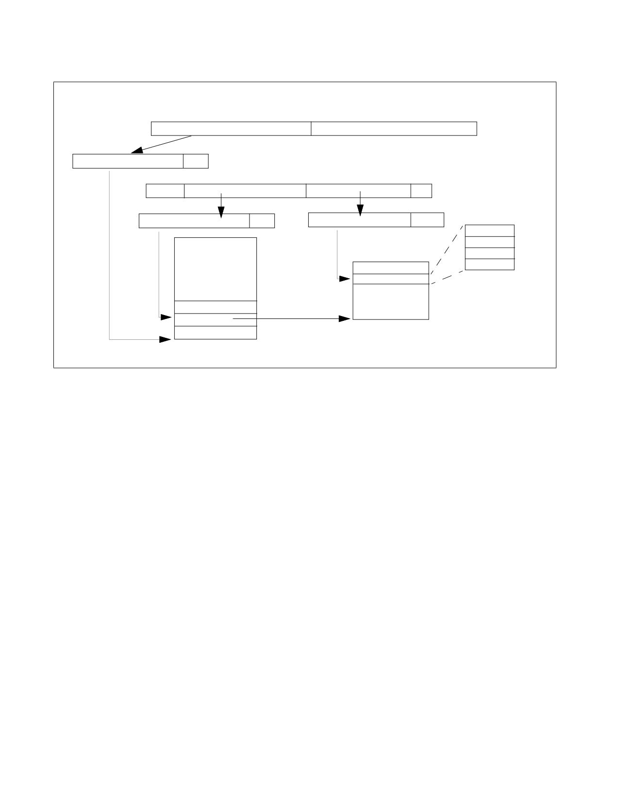
Figure E-4 shows the two-level structures for address translation of extended bounds in 64-bit mode.
Vol. 1
E-7
INTEL® MEMORY PROTECTION EXTENSIONS
BNDCFGU/BNDCFGS
63
12 11
0
Base of Bound Directory (Linear Address)
63
12
0
BNDCFGx[63:12]
0
Linear Address of “pointer” (LAp)
63
47+MAWA
20 19
3
0
30+MAWA
3
0
21
5
0
LAp[47+MAWA:20]
0
LAp[19:3]
0
Reserved
24
Pointer Value
16
64
22
Upper Bound
8
Lower Bound
31+MAWA
0
Bound Table Entries
Bound Directory Entries
61
0
Bound Table (4 MBytes)
0
Bound Directory (21+MAWA GBytes)
Figure E-4. Bound Paging Structure and Address Translation in 64-Bit Mode
As noted earlier, the linear address of the bound directory is derived from either BNDCFGU (CPL = 3) or BNDCFGS
(CPL < 3). In 64-bit mode, each bound-directory entry (BDE) is 8 bytes. The number of entries in the bound direc-
tory is determined by the MPX address-width adjust (MAWA; see Appendix E.3.1). Specifically, the number of
entries is 228+MAWA.
In 64-bit mode, the processor uses the two-level structures to access extended bounds as follows:
• A bound directory is located at the 4-KByte aligned linear address specified in bits 63:12 of BNDCFGx (see
Figure E-2). A bound directory comprises 228+MAWA 64-bit entries (BDEs); thus, the size of a bound directory
in 64-bit mode is 21+MAWA GBytes. A BDE is selected using the LAp (linear address of pointer to a buffer) to
construct a 64-bit offset as follows:
- bits 63:31+MAWA are 0;
- bits 30+MAWA:3 are LAp[47+MAWA:20]; and
- bits 2:0 are 0.
The address of the BDE is the sum of the bound-directory base address (from BNDCFGx) plus this 64-bit offset.
• Bit 0 of a BDE is a valid bit. If this bit is 0, use of the BDE by BNDLDX or BNDSTX causes #BR, sets
BNDSTATUS[1:0] to 10b (the error code), and loads BNDSTATUS[63:2] with bits 63:2 of the linear address of
the BDE. Otherwise, the processor uses bits 63:3 of the BDE as the 8-byte aligned address of a bound table
(BT); the processor ignores bits 2:1 of a BDE.
A bound table comprises 217 32-byte entries (BTEs); thus, the size of a bound table in 64-bit mode is 4 MBytes.
A BTE is selected using the LAp (linear address of pointer to a buffer) to construct an offset as follows:
- bits 21:5 are LAp[19:3]; and
- bits 4:0 are 0.
The address of the BTE is the sum of the bound-table base address (from the BDE) plus this offset.
• Each BTE comprises the following:
E-8
Vol. 1
INTEL® MEMORY PROTECTION EXTENSIONS
- a 64-bit lower bound (LB) field;
- a 64-bit upper bound (UB) field;
- a 64-bit pointer value; and
- a 64-bit reserved field. This field is reserved for future Intel MPX; software must not use it.
E.4.3.2
BNDLDX and BNDSTX Outside 64-Bit Mode
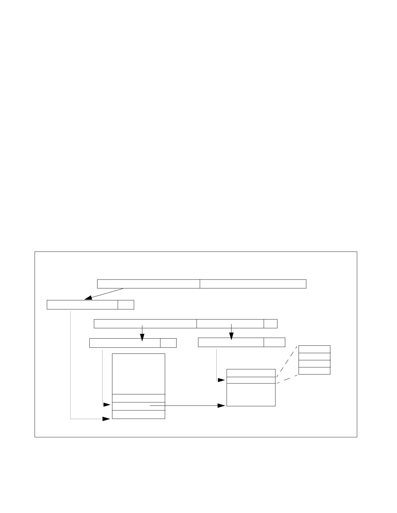
Figure E-5 shows the two-level structures for address translation of extended bounds outside 64-bit mode.
As noted earlier, the linear address of the bound directory is derived from either BNDCFGU (CPL = 3) or BNDCFGS
(CPL < 3). Outside 64-bit mode, each bound-directory entry (BDE) is 4 bytes. The number of entries in the bound
directory is 220.
Outside 64-bit mode, the processor uses the two-level structures to access extended bounds as follows:
• A bound directory is located at the 4-KByte aligned linear address specified in bits 31:12 of BNDCFGx (see
Figure E-2). A bound directory comprises 220 32-bit entries (BDEs); thus, the size of a bound directory outside
64-bit mode is 4 MBytes. A BDE is selected using the LAp (linear address of pointer to a buffer) to construct an
offset as follows:
- bits 21:2 are LAp[31:12]; and
- bits 1:0 are 0.
The address of the BDE is the sum of the bound-directory base address (from BNDCFGx) plus this offset.
• Bit 0 of a BDE is a valid bit. If this bit is 0, use of the BDE by BNDLDX or BNDSTX causes #BR, sets
BNDSTATUS[1:0] to 10b (the error code), and loads BNDSTATUS[31:2] with bits 31:2 of the linear address of
the BDE. Otherwise, the processor uses bits 31:2 of the BDE as the 4-byte aligned address of a bound table
(BT); the processor ignores bit 1 of a BDE.
BNDCFGU/BNDCFGS
31
12 11
0
Base of Bound Directory (Linear Address)
31
12
0
BNDCFGx[31:12]
0
Linear Address of “pointer” (LAp)
31
12 11
2
0
21
2
0
13
4
0
LAp[31:12]
0
LAp[11:2]
0
Reserved
12
Pointer Value
8
32
14
Upper Bound
4
Lower Bound
22
0
Bound Table Entries
Bound Directory Entries
30
0
Bound Table (16 KBytes)
0
Bound Directory (4 MBytes)
Figure E-5. Bound Paging Structure and Address Translation Outside 64-Bit Mode
Vol. 1
E-9

INTEL® MEMORY PROTECTION EXTENSIONS
A bound table comprises 210 16-byte entries (BTEs); thus, the size of a bound table outside 64-bit mode is
16 KBytes. A BTE is selected using the LAp (linear address of pointer to a buffer) to construct an offset as
follows:
- bits 13:4 are LAp[11:2]; and
- bits 3:0 are 0.
The address of the BTE is the sum of the bound-table base address (from the BDE) plus this offset. This address
is use as an offset into the DS segment to determine the linear address of the BTE.
• Each BTE comprises the following:
- a 32-bit lower bound (LB) field;
- a 32-bit upper bound (UB) field;
- a 32-bit pointer value; and
- a 32-bit reserved field. This field is reserved for future Intel MPX; software must not use it.
E.5
INTERACTIONS WITH INTEL MPX
E.5.1
Intel® MPX and Operating Modes
In 64-bit Mode, all Intel MPX instructions use 64-bit operands for bounds and 64 bit addressing, i.e., REX.W & 67H
have no effect on data or address size.
XSAVE, XSAVEOPT, and XRSTOR load/store 64-bit values in all modes, as these state-management instructions are
not Intel MPX instructions.
In compatibility and legacy modes (including 16-bit code segments, real and virtual 8086 modes) all Intel MPX
instructions use 32-bit operands for bounds and 32 bit addressing. The upper 32-bits of destination bound register
are cleared (consistent with behavior of integer registers)
In 32-bit and compatibility mode, the bounds are 32-bit, and are treated same as 32-bit integer registers. There-
fore, when 32-bit bound is updated in a bound register, the upper 32-bits are undefined. When switching from 64-
bit, the behavior of content of bounds register will be similar to that of general purpose registers.
Table E-3 describes the impact of 67H prefix on memory forms of Intel MPX instructions (register-only forms ignore
67H prefix) when Intel MPX is enabled:
Table E-3. Effective Address Size of Intel® MPX Instructions with 67H Prefix
Addressing Mode
67H Prefix
Effective Address Size used for Intel MPX instructions when Intel MPX is enabled
64-bit Mode
Y
64 bit addressing used
64-bit Mode
N
64 bit addressing used
32-bit Mode
Y
#UD
32-bit Mode
N
32 bit addressing used
16-bit Mode
Y
32 bit addressing used
16-bit Mode
N
#UD
E.5.2
Intel® MPX Support for Pointer Operations with Branching
Intel MPX provides flexibility in supporting pointer operation across control flow changes. Intel MPX allows
• compatibility with legacy code that may perform pointer operation across control flow changes and are unaware
of Intel MPX, along with
• Intel MPX-aware code that adds bounds checking protection to pointer operation across control flow changes.
E-10
Vol. 1

INTEL® MEMORY PROTECTION EXTENSIONS
The interface to provide such flexibility consists of:
• Using a prefix, referred to as BND prefix, to relevant branch instructions: CALL, RET, JMP, and Jcc.
• BNDCFGU and BNDCFGS provides the bit field, BNDPRESERVE (bit 1).
The value of BNDPRESERVE in conjunction with the presence/absence the BND prefix with those branching instruc-
tion will determine whether the values in BND0-BND3 will be initialized or unchanged.
E.5.3
CALL, RET, JMP, and All Jcc
An application compiled to use Intel MPX will use the REPNE (F2H) prefix (denoted by BND) for all forms of near
CALL, near RET, near JMP, short & near Jcc instructions (BND+CALL, BND+RET, BND+JMP, BND+Jcc). See Table
E-4 for specific opcodes. All far CALL, RET, and JMP instructions plus short JMP (JMP rel 8, opcode EB) instructions
will never cause bound registers to be initialized.
If BNDPRESERVE bit is one, above instructions will NOT INIT the bounds registers when BND prefix is not present
for above instructions (legacy behavior). However, If BNDPRESERVE is zero, above instructions will INIT ALL bound
registers (BND0-BND3) when BND prefix is not present for above instructions. If BND prefix is present for above
instructions, the BND registers will NOT INIT any bound registers (BND0-BND3).
The legacy code will continue to use non-prefixed forms of these instructions, so if BNDPRESERVE is zero, all the
bound registers will INIT by legacy code. This allows the legacy function to execute and return to callee with all
bound registers initialized (legacy code by definition cannot make or load bounds in bound registers because it
does not have Intel MPX instructions). This will eliminate compatibility concerns when legacy function might have
changed the pointer in registers but did not update the value of the bounds registers associated with these
pointers.
If BNDCFGx.BNDPRESERVE is clear then non-prefixed forms of these instructions will initialize all the bound regis-
ters. If this bit is set then non-prefixed and prefixed forms of these instructions will preserve the contents of bound
registers as shown in Table E-4.
Table E-4. Bounds Register INIT Behavior Due to BND Prefix with Branch Instructions
Instruction
Branch Instruction Opcodes
BNDPRESERVE = 0
BNDPRESERVE = 1
CALL
E8, FF/2
Init BND0-BND3
BND0-BND3 unchanged
BND + CALL
F2 E8, F2 FF/2
BND0-BND3 unchanged
BND0-BND3 unchanged
RET
C2, C3
Init BND0-BND3
BND0-BND3 unchanged
BND + RET
F2 C2, F2 C3
BND0-BND3 unchanged
BND0-BND3 unchanged
JMP
E9, FF/4
Init BND0-BND3
BND0-BND3 unchanged
BND + JMP
F2 E9, F2 FF/4
BND0-BND3 unchanged
BND0-BND3 unchanged
70 through 7F,
Jcc
Init BND0-BND3
BND0-BND3 unchanged
0F 80 through 0F 8F
F2 70 through F2 7F,
BND + Jcc
BND0-BND3 unchanged
BND0-BND3 unchanged
F2 0F 80 through F2 0F 8F
E.5.4
BOUND Instruction and Intel MPX
If Intel MPX in enabled (see Section 13.5) and a #BR was caused due to a BOUND instruction, then BOUND instruc-
tion will write zero to the BNDSTATUS register. In all other situations, BOUND instruction will not modify
BNDSTATUS. Specifically, the operation of the BOUND instruction can be described as:
IF ( ( BOUND instruction caused #BR) AND ( CR4.OXXSAVE = 1 AND XCR0.BNDREGS = 1 AND XCR0.BNDCSR = 1) AND
( (CPL= 3 AND BNDCFGU.ENABLE = 1) OR (CPL < 3 AND BNDCFGS.ENABLE = 1) ) ) THEN
BNDSTATUS := 0;
ELSE
BNDSTATUS is not modified;
FI;
Vol. 1
E-11
INTEL® MEMORY PROTECTION EXTENSIONS
E.5.5
Programming Considerations
Intel MPX instruction set does not dictate any calling convention, but allows the calling convention extensions to be
interoperable with legacy code by making use of the of the bound registers and the bound tables to convey argu-
ments and return values.
E.5.6
Intel MPX and System Management Mode
Upon delivery of an SMI to a processor supporting Intel MPX, the contents of IA32_BNDCFGS is saved to SMM state
save map (at offset 7ED0H) and the register is then cleared when entering into SMM. RSM restores IA32_BNDCFGS
from the SMM state save map. The instruction forces the reserved bits (11:2) to 0 and sign-extends the highest
implemented bit of the linear address to guarantee the canonicality of this address (regardless of what is in SMM
state save map).
The content of IA32_BNDCFGS is cleared after entering into SMM. Thus, Intel MPX is disabled inside an SMM
handler until SMM code enables it explicitly. This will prevent initialization of the bound registers by execution of
CALL, RET, JMP, or Jcc in SMM code.
E.5.7
Support of Intel MPX in VMCS
A new guest-state field for IA32_BNDCFGS is added to the VMCS. In addition, two new controls are added:
• a VM-exit control called “clear BNDCFGS”
• a VM-entry control called “load BNDCFGS.”
VM exits always save IA32_BNDCFGS into BNDCFGS field of VMCS; if “clear BNDCFGS” is 1, VM exits clear IA32_B-
NDCFGS. If “load BNDCFGS” is 1, VM entry loads IA32_BNDCFGS from VMCS. If loading IA32_BNDCFGS, VM entry
should check the value of that register in the guest-state area of the VMCS and cause the VM entry to fail (late) if
the value is one that would causes WRMSR to fault if executed in ring 0.
E.5.8
Support of Intel MPX in Intel TSX
For some processor implementations, the following Intel MPX instructions may always cause transactional aborts:
• An Intel TSX transaction abort will occur in case of legacy branch (that causes bounds registers INIT) when at
least one bounds register was in a NON-INIT state.
• An Intel TSX transaction abort will occur in case of a BNDLDX & BNDSTX instruction on non-flat segment.
Intel MPX Instructions (including BND prefix + branch instructions) not enumerated above as causing transactional
abort when used inside a transaction will typically not cause an Intel TSX transaction to abort.
E-12
Vol. 1

Intel® 64 and IA-32 Architectures
Software Developer’s Manual
Volume 2 (2A, 2B, 2C, & 2D):
Instruction Set Reference, A-Z
NOTE: The Intel 64 and IA-32 Architectures Software Developer's Manual consists of four volumes:
Basic Architecture, Order Number 253665; Instruction Set Reference, A-Z, Order Number 325383;
System Programming Guide, Order Number 325384; Model-Specific Registers, Order Number
335592. Refer to all four volumes when evaluating your design needs.
Order Number: 325383-092US
June 2026
Notices & Disclaimers
Intel technologies may require enabled hardware, software or service activation.
No product or component can be absolutely secure.
Your costs and results may vary.
You may not use or facilitate the use of this document in connection with any infringement or other legal analysis concerning
Intel products described herein. You agree to grant Intel a non-exclusive, royalty-free license to any patent claim thereafter
drafted which includes subject matter disclosed herein.
All product plans and roadmaps are subject to change without notice.
The products described may contain design defects or errors known as errata which may cause the product to deviate from
published specifications. Current characterized errata are available on request.
Intel disclaims all express and implied warranties, including without limitation, the implied warranties of merchantability,
fitness for a particular purpose, and non-infringement, as well as any warranty arising from course of performance, course of
dealing, or usage in trade.
Code names are used by Intel to identify products, technologies, or services that are in development and not publicly
available. These are not “commercial” names and not intended to function as trademarks.
No license (express or implied, by estoppel or otherwise) to any intellectual property rights is granted by this document, with
the sole exception that a) you may publish an unmodified copy and b) code, identified as Sample Code in this document is
licensed subject to the Zero-Clause BSD open source license (0BSD), https://opensource.org/licenses/0BSD. You may create
software implementations based on this document and in compliance with the foregoing that are intended to execute on the
Intel product(s) referenced in this document. No rights are granted to create modifications or derivatives of this document.
© Intel Corporation. Intel, the Intel logo, and other Intel marks are trademarks of Intel Corporation or its subsidiaries. Other
names and brands may be claimed as the property of others.
CONTENTS
PAGE
CHAPTER 1
ABOUT THIS MANUAL
1.1
OVERVIEW OF VOLUME 2A, 2B, 2C, AND 2D: INSTRUCTION SET REFERENCE
1-1
CHAPTER 2
INSTRUCTION FORMAT
2.1
INSTRUCTION FORMAT FOR PROTECTED MODE, REAL-ADDRESS MODE, AND VIRTUAL-8086 MODE
2-1
2.1.1
Instruction Prefixes
2-1
2.1.2
Opcodes
2-2
2.1.3
ModR/M and SIB Bytes
2-3
2.1.4
Displacement and Immediate Bytes
2-3
2.1.5
Addressing-Mode Encoding of ModR/M and SIB Bytes
2-3
2.2
IA-32E MODE
2-7
2.2.1
REX Prefixes
2-7
2.2.1.1
Encoding
2-8
2.2.1.2
More on REX Prefix Fields
2-8
2.2.1.3
Displacement
2-11
2.2.1.4
Direct Memory-Offset MOVs
2-11
2.2.1.5
Immediates
2-11
2.2.1.6
RIP-Relative Addressing
2-11
2.2.1.7
Default 64-Bit Operand Size
2-12
2.2.2
Additional Encodings for Control and Debug Registers
2-12
2.3
INTEL® ADVANCED VECTOR EXTENSIONS (INTEL® AVX)
2-12
2.3.1
Instruction Format
2-12
2.3.2
VEX and the LOCK prefix
2-13
2.3.3
VEX and the 66H, F2H, and F3H prefixes
2-13
2.3.4
VEX and the REX prefix
2-13
2.3.5
The VEX Prefix
2-13
2.3.5.1
VEX Byte 0, bits[7:0]
2-15
2.3.5.2
VEX Byte 1, bit [7] - ‘R’
2-15
2.3.5.3
3-byte VEX byte 1, bit[6] - ‘X’
2-16
2.3.5.4
3-byte VEX byte 1, bit[5] - ‘B’
2-16
2.3.5.5
3-byte VEX byte 2, bit[7] - ‘W’
2-16
2.3.5.6
2-byte VEX Byte 1, bits[6:3] and 3-byte VEX Byte 2, bits [6:3]- ‘vvvv’ the Source or Dest Register Specifier
2-16
2.3.6
Instruction Operand Encoding and VEX.vvvv, ModR/M
2-17
2.3.6.1
3-byte VEX byte 1, bits[4:0] - “m-mmmm”
2-18
2.3.6.2
2-byte VEX byte 1, bit[2], and 3-byte VEX byte 2, bit [2]- “L”
2-18
2.3.6.3
2-byte VEX byte 1, bits[1:0], and 3-byte VEX byte 2, bits [1:0]- “pp”
2-19
2.3.7
The Opcode Byte
2-19
2.3.8
The ModR/M, SIB, and Displacement Bytes
2-19
2.3.9
The Third Source Operand (Immediate Byte)
2-19
2.3.10
Intel® AVX Instructions and the Upper 128-bits of YMM registers
2-19
2.3.10.1
Vector Length Transition and Programming Considerations
2-19
2.3.11
Intel® AVX Instruction Length
2-20
2.3.12
Vector SIB (VSIB) Memory Addressing
2-20
2.3.12.1
64-bit Mode VSIB Memory Addressing
2-21
2.4
INTEL® ADVANCED MATRIX EXTENSIONS (INTEL® AMX)
2-21
2.5
INTEL® AVX AND INTEL® SSE INSTRUCTION EXCEPTION CLASSIFICATION
2-22
2.5.1
Exceptions Type 1 (Aligned Memory Reference)
2-26
2.5.2
Exceptions Type 2 (>=16 Byte Memory Reference, Unaligned)
2-26
2.5.3
Exceptions Type 3 (<16 Byte Memory Argument)
2-27
2.5.4
Exceptions Type 4 (>=16 Byte Mem Arg, No Alignment, No Floating-point Exceptions)
2-28
2.5.5
Exceptions Type 5 (<16 Byte Mem Arg and No FP Exceptions)
2-29
2.5.6
Exceptions Type 6 (VEX-Encoded Instructions without Legacy SSE Analogues)
2-30
2.5.7
Exceptions Type 7 (No FP Exceptions, No Memory Arg)
2-32
2.5.8
Exceptions Type 8 (AVX and No Memory Argument)
2-32
2.5.9
Exceptions Type 11 (VEX-only, Mem Arg, No AC, Floating-point Exceptions)
2-32
2.5.10
Exceptions Type 12 (VEX-only, VSIB Mem Arg, No AC, No Floating-point Exceptions)
2-33
2.6
VEX ENCODING SUPPORT FOR GPR INSTRUCTIONS
2-34
2.6.1
Exceptions Type 13 (VEX-Encoded GPR Instructions)
2-35
Vol. 2A iii
CONTENTS
PAGE
2.6.2
Exceptions Type 14 (CMPCCXADD)
2-35
2.7
INTEL® AVX-512 ENCODING
2-36
2.7.1
Instruction Format and EVEX
2-36
2.7.2
Register Specifier Encoding and EVEX
2-39
2.7.3
Opmask Register Encoding
2-40
2.7.4
Masking Support in EVEX
2-40
2.7.5
Compressed Displacement (disp8*N) Support in EVEX
2-41
2.7.6
EVEX Encoding of Broadcast/Rounding/SAE Support
2-42
2.7.7
Embedded Broadcast Support in EVEX
2-42
2.7.8
Static Rounding Support in EVEX
2-42
2.7.9
SAE Support in EVEX
2-42
2.7.10
Vector Length Orthogonality
2-42
2.7.11
#UD Equations for EVEX
2-43
2.7.11.1
State Dependent #UD
2-43
2.7.11.2
Opcode Independent #UD
2-43
2.7.11.3
Opcode Dependent #UD
2-44
2.7.12
Device Not Available
2-45
2.7.13
Scalar Instructions
2-45
2.8
EXCEPTION CLASSIFICATIONS OF EVEX-ENCODED INSTRUCTIONS
2-45
2.8.1
Exceptions Type E1 and E1NF of EVEX-Encoded Instructions
2-48
2.8.2
Exceptions Type E2 of EVEX-Encoded Instructions
2-50
2.8.3
Exceptions Type E3 and E3NF of EVEX-Encoded Instructions
2-51
2.8.4
Exceptions Type E4 and E4NF of EVEX-Encoded Instructions
2-53
2.8.5
Exceptions Type E5 and E5NF
2-55
2.8.6
Exceptions Type E6 and E6NF
2-58
2.8.7
Exceptions Type E7NM
2-59
2.8.8
Exceptions Type E9 and E9NF
2-60
2.8.9
Exceptions Type E10 and E10NF
2-62
2.8.10
Exceptions Type E11 (EVEX-only, Mem Arg, No AC, Floating-point Exceptions)
2-64
2.8.11
Exceptions Type E12 and E12NP (VSIB Mem Arg, No AC, No Floating-point Exceptions)
2-66
2.9
EXCEPTION CLASSIFICATIONS OF OPMASK INSTRUCTIONS, TYPE K20 AND TYPE K21
2-67
2.9.1
Exceptions Type K20
2-67
2.9.2
Exceptions Type K21
2-68
2.10
INTEL® AMX INSTRUCTION EXCEPTION CLASSES
2-69
CHAPTER 3
INSTRUCTION SET REFERENCE, A-L
3.1
INTERPRETING THE INSTRUCTION REFERENCE PAGES
3-1
3.1.1
Instruction Format
3-1
3.1.1.1
Opcode Column in the Instruction Summary Table (Instructions without VEX Prefix)
3-2
3.1.1.2
Opcode Column in the Instruction Summary Table (Instructions with VEX prefix)
3-3
3.1.1.3
Instruction Column in the Opcode Summary Table
3-5
3.1.1.4
Operand Encoding Column in the Instruction Summary Table
3-8
3.1.1.5
64/32-bit Mode Column in the Instruction Summary Table
3-8
3.1.1.6
CPUID Support Column in the Instruction Summary Table
3-9
3.1.1.7
Description Column in the Instruction Summary Table
3-9
3.1.1.8
Description Section
3-9
3.1.1.9
Operation Section
3-9
3.1.1.10
Intel® C/C++ Compiler Intrinsics Equivalents Section
3-12
3.1.1.11
Flags Affected Section
3-14
3.1.1.12
FPU Flags Affected Section
3-15
3.1.1.13
Protected Mode Exceptions Section
3-15
3.1.1.14
Real-Address Mode Exceptions Section
3-16
3.1.1.15
Virtual-8086 Mode Exceptions Section
3-16
3.1.1.16
Floating-Point Exceptions Section
3-16
3.1.1.17
SIMD Floating-Point Exceptions Section
3-16
3.1.1.18
Compatibility Mode Exceptions Section
3-17
3.1.1.19
64-Bit Mode Exceptions Section
3-17
3.2
INTEL® AMX CONSIDERATIONS
3-17
3.2.1
Implementation Parameters
3-17
3.2.2
Helper Functions
3-17
3.3
INSTRUCTIONS (A-L)
3-18
AAA-ASCII Adjust After Addition
3-1
AAD-ASCII Adjust AX Before Division
3-3
iv Vol. 2A
CONTENTS
PAGE
AAM-ASCII Adjust AX After Multiply
3-5
AAS-ASCII Adjust AL After Subtraction
3-7
ADC-Add With Carry
3-9
ADCX-Unsigned Integer Addition of Two Operands With Carry Flag
3-12
ADD-Add
3-14
ADDPD-Add Packed Double Precision Floating-Point Values
3-16
ADDPS-Add Packed Single Precision Floating-Point Values
3-19
ADDSD-Add Scalar Double Precision Floating-Point Values
3-22
ADDSS-Add Scalar Single Precision Floating-Point Values
3-24
ADDSUBPD-Packed Double Precision Floating-Point Add/Subtract
3-26
ADDSUBPS-Packed Single Precision Floating-Point Add/Subtract
3-28
ADOX - Unsigned Integer Addition of Two Operands With Overflow Flag
3-31
AESDEC-Perform One Round of an AES Decryption Flow
3-33
AESDEC128KL-Perform Ten Rounds of AES Decryption Flow With Key Locker Using 128-Bit Key
3-35
AESDEC256KL-Perform 14 Rounds of AES Decryption Flow With Key Locker Using 256-Bit Key
3-37
AESDECLAST-Perform Last Round of an AES Decryption Flow
3-39
AESDECWIDE128KL-Perform Ten Rounds of AES Decryption Flow With Key Locker on 8 Blocks Using 128-Bit Key 3-41
AESDECWIDE256KL-Perform 14 Rounds of AES Decryption Flow With Key Locker on 8 Blocks Using 256-Bit Key . 3-43
AESENC-Perform One Round of an AES Encryption Flow
3-45
AESENC128KL-Perform Ten Rounds of AES Encryption Flow With Key Locker Using 128-Bit Key
3-47
AESENC256KL-Perform 14 Rounds of AES Encryption Flow With Key Locker Using 256-Bit Key
3-49
AESENCLAST-Perform Last Round of an AES Encryption Flow
3-51
AESENCWIDE128KL-Perform Ten Rounds of AES Encryption Flow With Key Locker on 8 Blocks Using 128-Bit Key 3-53
AESENCWIDE256KL-Perform 14 Rounds of AES Encryption Flow With Key Locker on 8 Blocks Using 256-Bit Key . 3-55
AESIMC-Perform the AES InvMixColumn Transformation
3-57
AESKEYGENASSIST-AES Round Key Generation Assist
3-58
AND-Logical AND
3-60
ANDN-Logical AND NOT
3-62
ANDNPD-Bitwise Logical AND NOT of Packed Double Precision Floating-Point Values
3-63
ANDNPS-Bitwise Logical AND NOT of Packed Single Precision Floating-Point Values
3-66
ANDPD-Bitwise Logical AND of Packed Double Precision Floating-Point Values
3-69
ANDPS-Bitwise Logical AND of Packed Single Precision Floating-Point Values
3-72
ARPL-Adjust RPL Field of Segment Selector
3-75
BEXTR-Bit Field Extract
3-77
BLENDPD-Blend Packed Double Precision Floating-Point Values
3-78
BLENDPS-Blend Packed Single Precision Floating-Point Values
3-80
BLENDVPD-Variable Blend Packed Double Precision Floating-Point Values
3-82
BLENDVPS-Variable Blend Packed Single Precision Floating-Point Values
3-84
BLSI-Extract Lowest Set Isolated Bit
3-87
BLSMSK-Get Mask Up to Lowest Set Bit
3-88
BLSR-Reset Lowest Set Bit
3-89
BNDCL-Check Lower Bound
3-90
BNDCU/BNDCN-Check Upper Bound
3-92
BNDLDX-Load Extended Bounds Using Address Translation
3-94
BNDMK-Make Bounds
3-97
BNDMOV-Move Bounds
3-99
BNDSTX-Store Extended Bounds Using Address Translation
3-102
BOUND-Check Array Index Against Bounds
3-105
BSF-Bit Scan Forward
3-107
BSR-Bit Scan Reverse
3-109
BSWAP-Byte Swap
3-111
BT-Bit Test
3-112
BTC-Bit Test and Complement
3-114
BTR-Bit Test and Reset
3-116
BTS-Bit Test and Set
3-118
BZHI-Zero High Bits Starting with Specified Bit Position
3-120
CALL-Call Procedure
3-121
CBW/CWDE/CDQE-Convert Byte to Word/Convert Word to Doubleword/Convert Doubleword to Quadword
3-138
CLAC-Clear AC Flag in EFLAGS Register
3-139
Vol. 2A v
CONTENTS
PAGE
CLC-Clear Carry Flag
3-140
CLD-Clear Direction Flag
3-141
CLDEMOTE-Cache Line Demote
3-142
CLFLUSH-Flush Cache Line
3-144
CLFLUSHOPT-Flush Cache Line Optimized
3-146
CLI-Clear Interrupt Flag
3-148
CLRSSBSY-Clear Busy Flag in a Supervisor Shadow Stack Token
3-150
CLTS-Clear Task-Switched Flag in CR0
3-152
CLUI-Clear User Interrupt Flag
3-153
CLWB-Cache Line Write Back
3-154
CMC-Complement Carry Flag
3-156
CMOVcc-Conditional Move
3-157
CMP-Compare Two Operands
3-161
CMPccXADD-Compare and Add if Condition is Met
3-163
CMPPD-Compare Packed Double Precision Floating-Point Values
3-168
CMPPS-Compare Packed Single Precision Floating-Point Values
3-175
CMPS/CMPSB/CMPSW/CMPSD/CMPSQ-Compare String Operands
3-181
CMPSD-Compare Scalar Double Precision Floating-Point Value
3-185
CMPSS-Compare Scalar Single Precision Floating-Point Value
3-189
CMPXCHG-Compare and Exchange
3-194
CMPXCHG8B/CMPXCHG16B-Compare and Exchange Bytes
3-196
COMISD-Compare Scalar Ordered Double Precision Floating-Point Values and Set EFLAGS
3-199
COMISS-Compare Scalar Ordered Single Precision Floating-Point Values and Set EFLAGS
3-201
CPUID-CPU Identification
3-203
CRC32-Accumulate CRC32 Value
3-205
CVTDQ2PD-Convert Packed Doubleword Integers to Packed Double Precision Floating-Point Values
3-208
CVTDQ2PS-Convert Packed Doubleword Integers to Packed Single Precision Floating-Point Values
3-211
CVTPD2DQ-Convert Packed Double Precision Floating-Point Values to Packed Doubleword Integers
3-214
CVTPD2PI-Convert Packed Double Precision Floating-Point Values to Packed Dword Integers
3-218
CVTPD2PS-Convert Packed Double Precision Floating-Point Values to Packed Single Precision
Floating-Point Values
3-219
CVTPI2PD-Convert Packed Dword Integers to Packed Double Precision Floating-Point Values
3-223
CVTPI2PS-Convert Packed Dword Integers to Packed Single Precision Floating-Point Values
3-224
CVTPS2DQ-Convert Packed Single Precision Floating-Point Values to Packed Signed Doubleword Integer Values . 3-225
CVTPS2PD-Convert Packed Single Precision Floating-Point Values to Packed Double Precision
Floating-Point Values
3-228
CVTPS2PI-Convert Packed Single Precision Floating-Point Values to Packed Dword Integers
3-231
CVTSD2SI-Convert Scalar Double Precision Floating-Point Value to Signed Integer
3-232
CVTSD2SS-Convert Scalar Double Precision Floating-Point Value to Scalar Single Precision Floating-Point Value . . 3-234
CVTSI2SD-Convert Signed Integer to Scalar Double Precision Floating-Point Value
3-236
CVTSI2SS-Convert Signed Integer to Scalar Single Precision Floating-Point Value
3-238
CVTSS2SD-Convert Scalar Single Precision Floating-Point Value to Scalar Double Precision Floating-Point Value . . 3-240
CVTSS2SI-Convert Scalar Single Precision Floating-Point Value to Signed Integer
3-242
CVTTPD2DQ-Convert with Truncation Packed Double Precision Floating-Point Values to Packed Doubleword
Integers
3-244
CVTTPD2PI-Convert With Truncation Packed Double Precision Floating-Point Values to Packed Dword Integers . . 3-248
CVTTPS2DQ-Convert With Truncation Packed Single Precision Floating-Point Values to Packed Signed
Doubleword Integer Values
3-249
CVTTPS2PI-Convert With Truncation Packed Single Precision Floating-Point Values to Packed Dword Integers . . . 3-252
CVTTSD2SI-Convert With Truncation Scalar Double Precision Floating-Point Value to Signed Integer
3-253
CVTTSS2SI-Convert With Truncation Scalar Single Precision Floating-Point Value to Signed Integer
3-255
CWD/CDQ/CQO-Convert Word to Doubleword/Convert Doubleword to Quadword
3-257
DAA-Decimal Adjust AL After Addition
3-258
DAS-Decimal Adjust AL After Subtraction
3-260
DEC-Decrement by 1
3-262
DIV-Unsigned Divide
3-264
DIVPD-Divide Packed Double Precision Floating-Point Values
3-267
DIVPS-Divide Packed Single Precision Floating-Point Values
3-270
DIVSD-Divide Scalar Double Precision Floating-Point Value
3-273
vi Vol. 2A
CONTENTS
PAGE
DIVSS-Divide Scalar Single Precision Floating-Point Values
3-275
DPPD-Dot Product of Packed Double Precision Floating-Point Values
3-277
DPPS-Dot Product of Packed Single Precision Floating-Point Values
3-279
EMMS-Empty MMX Technology State
3-282
ENCODEKEY128-Encode 128-Bit Key With Key Locker
3-283
ENCODEKEY256-Encode 256-Bit Key With Key Locker
3-285
ENDBR32-Terminate an Indirect Branch in 32-bit and Compatibility Mode
3-287
ENDBR64-Terminate an Indirect Branch in 64-bit Mode
3-288
ENQCMD-Enqueue Command
3-289
ENQCMDS-Enqueue Command Supervisor
3-292
ENTER-Make Stack Frame for Procedure Parameters
3-295
ERETS-Event Return to Supervisor
3-298
ERETU-Event Return to User
3-301
EXTRACTPS-Extract Packed Floating-Point Values
3-305
F2XM1-Compute 2x-1
3-307
FABS-Absolute Value
3-309
FADD/FADDP/FIADD-Add
3-311
FBLD-Load Binary Coded Decimal
3-314
FBSTP-Store BCD Integer and Pop
3-316
FCHS-Change Sign
3-318
FCLEX/FNCLEX-Clear Exceptions
3-320
FCMOVcc-Floating-Point Conditional Move
3-322
FCOM/FCOMP/FCOMPP-Compare Floating-Point Values
3-324
FCOMI/FCOMIP/ FUCOMI/FUCOMIP-Compare Floating-Point Values and Set EFLAGS
3-327
FCOS-Cosine
3-330
FDECSTP-Decrement Stack-Top Pointer
3-332
FDIV/FDIVP/FIDIV-Divide
3-333
FDIVR/FDIVRP/FIDIVR-Reverse Divide
3-336
FFREE-Free Floating-Point Register
3-339
FICOM/FICOMP-Compare Integer
3-340
FILD-Load Integer
3-342
FINCSTP-Increment Stack-Top Pointer
3-344
FINIT/FNINIT-Initialize Floating-Point Unit
3-345
FIST/FISTP-Store Integer
3-347
FISTTP-Store Integer With Truncation
3-350
FLD-Load Floating-Point Value
3-352
FLD1/FLDL2T/FLDL2E/FLDPI/FLDLG2/FLDLN2/FLDZ-Load Constant
3-354
FLDCW-Load x87 FPU Control Word
3-356
FLDENV-Load x87 FPU Environment
3-358
FMUL/FMULP/FIMUL-Multiply
3-360
FNOP-No Operation
3-363
FPATAN-Partial Arctangent
3-364
FPREM-Partial Remainder
3-366
FPREM1-Partial Remainder
3-368
FPTAN-Partial Tangent
3-370
FRNDINT-Round to Integer
3-372
FRSTOR-Restore x87 FPU State
3-373
FSAVE/FNSAVE-Store x87 FPU State
3-375
FSCALE-Scale
3-378
FSIN-Sine
3-380
FSINCOS-Sine and Cosine
3-382
FSQRT-Square Root
3-384
FST/FSTP-Store Floating-Point Value
3-386
FSTCW/FNSTCW-Store x87 FPU Control Word
3-388
FSTENV/FNSTENV-Store x87 FPU Environment
3-390
FSTSW/FNSTSW-Store x87 FPU Status Word
3-392
FSUB/FSUBP/FISUB-Subtract
3-394
FSUBR/FSUBRP/FISUBR-Reverse Subtract
3-397
FTST-TEST
3-400
Vol. 2A vii
CONTENTS
PAGE
FUCOM/FUCOMP/FUCOMPP-Unordered Compare Floating-Point Values
3-402
FXAM-Examine Floating-Point
3-405
FXCH-Exchange Register Contents
3-407
FXRSTOR-Restore x87 FPU, MMX, XMM, and MXCSR State
3-409
FXSAVE-Save x87 FPU, MMX Technology, and SSE State
3-412
FXTRACT-Extract Exponent and Significand
3-420
FYL2X-Compute y * log2x
3-422
FYL2XP1-Compute y * log2(x +1)
3-424
GF2P8AFFINEINVQB-Galois Field Affine Transformation Inverse
3-426
GF2P8AFFINEQB-Galois Field Affine Transformation
3-429
GF2P8MULB-Galois Field Multiply Bytes
3-431
HADDPD-Packed Double Precision Floating-Point Horizontal Add
3-433
HADDPS-Packed Single Precision Floating-Point Horizontal Add
3-436
HLT-Halt
3-439
HRESET-History Reset
3-440
HSUBPD-Packed Double Precision Floating-Point Horizontal Subtract
3-442
HSUBPS-Packed Single Precision Floating-Point Horizontal Subtract
3-445
IDIV-Signed Divide
3-448
IMUL-Signed Multiply
3-451
IN-Input From Port
3-455
INC-Increment by 1
3-457
INCSSPD/INCSSPQ-Increment Shadow Stack Pointer
3-459
INSERTPS-Insert Scalar Single Precision Floating-Point Value
3-461
INS/INSB/INSW/INSD-Input from Port to String
3-464
INT n/INTO/INT3/INT1-Call to Interrupt Procedure
3-467
INVD-Invalidate Internal Caches
3-483
INVLPG-Invalidate TLB Entries
3-485
INVPCID-Invalidate Process-Context Identifier
3-487
IRET/IRETD/IRETQ-Interrupt Return
3-490
Jcc-Jump if Condition Is Met
3-499
JMP-Jump
3-504
KADDW/KADDB/KADDQ/KADDD-ADD Two Masks
3-513
KANDNW/KANDNB/KANDNQ/KANDND-Bitwise Logical AND NOT Masks
3-515
KANDW/KANDB/KANDQ/KANDD-Bitwise Logical AND Masks
3-516
KMOVW/KMOVB/KMOVQ/KMOVD-Move From and to Mask Registers
3-517
KNOTW/KNOTB/KNOTQ/KNOTD-NOT Mask Register
3-519
KORTESTW/KORTESTB/KORTESTQ/KORTESTD-OR Masks and Set Flags
3-520
KORW/KORB/KORQ/KORD-Bitwise Logical OR Masks
3-522
KSHIFTLW/KSHIFTLB/KSHIFTLQ/KSHIFTLD-Shift Left Mask Registers
3-523
KSHIFTRW/KSHIFTRB/KSHIFTRQ/KSHIFTRD-Shift Right Mask Registers
3-525
KTESTW/KTESTB/KTESTQ/KTESTD-Packed Bit Test Masks and Set Flags
3-527
KUNPCKBW/KUNPCKWD/KUNPCKDQ-Unpack for Mask Registers
3-529
KXNORW/KXNORB/KXNORQ/KXNORD-Bitwise Logical XNOR Masks
3-530
KXORW/KXORB/KXORQ/KXORD-Bitwise Logical XOR Masks
3-531
LAHF-Load Status Flags Into AH Register
3-532
LAR-Load Access Rights
3-533
LDDQU-Load Unaligned Integer 128 Bits
3-537
LDMXCSR-Load MXCSR Register
3-539
LDS/LES/LFS/LGS/LSS-Load Far Pointer
3-540
LDTILECFG-Load Tile Configuration
3-544
LEA-Load Effective Address
3-547
LEAVE-High Level Procedure Exit
3-550
LFENCE-Load Fence
3-552
LGDT/LIDT-Load Global/Interrupt Descriptor Table Register
3-553
LKGS-Load Kernel GS Base
3-556
LLDT-Load Local Descriptor Table Register
3-558
LMSW-Load Machine Status Word
3-560
LOADIWKEY-Load Internal Wrapping Key With Key Locker
3-562
LOCK-Assert LOCK# Signal Prefix
3-565
viii Vol. 2A
CONTENTS
PAGE
LODS/LODSB/LODSW/LODSD/LODSQ-Load String
3-567
LOOP/LOOPcc-Loop According to ECX Counter
3-570
LSL-Load Segment Limit
3-573
LTR-Load Task Register
3-576
LZCNT-Count the Number of Leading Zero Bits
3-578
CHAPTER 4
INSTRUCTION SET REFERENCE, M-U
4.1
IMM8 CONTROL BYTE OPERATION FOR PCMPESTRI / PCMPESTRM / PCMPISTRI / PCMPISTRM
4-1
4.1.1
General Description
4-1
4.1.2
Source Data Format
4-1
4.1.3
Aggregation Operation
4-2
4.1.4
Polarity
4-2
4.1.5
Output Selection
4-3
4.1.6
Valid/Invalid Override of Comparisons
4-3
4.1.7
Summary of Im8 Control byte
4-4
4.1.8
Diagram Comparison and Aggregation Process
4-5
4.2
COMMON TRANSFORMATION AND PRIMITIVE FUNCTIONS FOR SHA1XXX AND SHA256XXX
4-5
4.3
INSTRUCTIONS (M-U)
4-6
MASKMOVDQU-Store Selected Bytes of Double Quadword
4-1
MASKMOVQ-Store Selected Bytes of Quadword
4-3
MAXPD-Maximum of Packed Double Precision Floating-Point Values
4-5
MAXPS-Maximum of Packed Single Precision Floating-Point Values
4-8
MAXSD-Return Maximum Scalar Double Precision Floating-Point Value
4-11
MAXSS-Return Maximum Scalar Single Precision Floating-Point Value
4-13
MFENCE-Memory Fence
4-15
MINPD-Minimum of Packed Double Precision Floating-Point Values
4-16
MINPS-Minimum of Packed Single Precision Floating-Point Values
4-19
MINSD-Return Minimum Scalar Double Precision Floating-Point Value
4-22
MINSS-Return Minimum Scalar Single Precision Floating-Point Value
4-24
MONITOR-Set Up Monitor Address
4-26
MOV-Move
4-28
MOV-Move to/from Control Registers
4-32
MOV-Move to/from Debug Registers
4-35
MOVAPD-Move Aligned Packed Double Precision Floating-Point Values
4-37
MOVAPS-Move Aligned Packed Single Precision Floating-Point Values
4-41
MOVBE-Move Data After Swapping Bytes
4-45
MOVDDUP-Replicate Double Precision Floating-Point Values
4-47
MOVDIR64B-Move 64 Bytes as Direct Store
4-50
MOVDIRI-Move Doubleword as Direct Store
4-52
MOVD/MOVQ-Move Doubleword/Move Quadword
4-54
MOVDQ2Q-Move Quadword from XMM to MMX Technology Register
4-58
MOVDQA,VMOVDQA32/64-Move Aligned Packed Integer Values
4-59
MOVDQU,VMOVDQU8/16/32/64-Move Unaligned Packed Integer Values
4-64
MOVHLPS-Move Packed Single Precision Floating-Point Values High to Low
4-72
MOVHPD-Move High Packed Double Precision Floating-Point Value
4-74
MOVHPS-Move High Packed Single Precision Floating-Point Values
4-76
MOVLHPS-Move Packed Single Precision Floating-Point Values Low to High
4-78
MOVLPD-Move Low Packed Double Precision Floating-Point Value
4-80
MOVLPS-Move Low Packed Single Precision Floating-Point Values
4-82
MOVMSKPD-Extract Packed Double Precision Floating-Point Sign Mask
4-84
MOVMSKPS-Extract Packed Single Precision Floating-Point Sign Mask
4-86
MOVNTDQ-Store Packed Integers Using Non-Temporal Hint
4-88
MOVNTDQA-Load Double Quadword Non-Temporal Aligned Hint
4-90
MOVNTI-Store Doubleword Using Non-Temporal Hint
4-92
MOVNTPD-Store Packed Double Precision Floating-Point Values Using Non-Temporal Hint
4-94
MOVNTPS-Store Packed Single Precision Floating-Point Values Using Non-Temporal Hint
4-96
MOVNTQ-Store of Quadword Using Non-Temporal Hint
4-98
MOVQ-Move Quadword
4-99
MOVQ2DQ-Move Quadword from MMX Technology to XMM Register
4-102
Vol. 2A ix
CONTENTS
PAGE
MOVS/MOVSB/MOVSW/MOVSD/MOVSQ-Move Data From String to String
4-104
MOVSD-Move or Merge Scalar Double Precision Floating-Point Value
4-108
MOVSHDUP-Replicate Single Precision Floating-Point Values
4-111
MOVSLDUP-Replicate Single Precision Floating-Point Values
4-114
MOVSS-Move or Merge Scalar Single Precision Floating-Point Value
4-117
MOVSX/MOVSXD-Move With Sign-Extension
4-120
MOVUPD-Move Unaligned Packed Double Precision Floating-Point Values
4-122
MOVUPS-Move Unaligned Packed Single Precision Floating-Point Values
4-126
MOVZX-Move With Zero-Extend
4-130
MPSADBW-Compute Multiple Packed Sums of Absolute Difference
4-132
MUL-Unsigned Multiply
4-140
MULPD-Multiply Packed Double Precision Floating-Point Values
4-142
MULPS-Multiply Packed Single Precision Floating-Point Values
4-145
MULSD-Multiply Scalar Double Precision Floating-Point Value
4-148
MULSS-Multiply Scalar Single Precision Floating-Point Values
4-150
MULX-Unsigned Multiply Without Affecting Flags
4-152
MWAIT-Monitor Wait
4-154
NEG-Two's Complement Negation
4-158
NOP-No Operation
4-160
NOT-One's Complement Negation
4-161
OR-Logical Inclusive OR
4-163
ORPD-Bitwise Logical OR of Packed Double Precision Floating-Point Values
4-165
ORPS-Bitwise Logical OR of Packed Single Precision Floating-Point Values
4-168
OUT-Output to Port
4-171
OUTS/OUTSB/OUTSW/OUTSD-Output String to Port
4-173
PABSB/PABSW/PABSD/PABSQ-Packed Absolute Value
4-177
PACKSSWB/PACKSSDW-Pack With Signed Saturation
4-183
PACKUSDW-Pack With Unsigned Saturation
4-191
PACKUSWB-Pack With Unsigned Saturation
4-196
PADDB/PADDW/PADDD/PADDQ-Add Packed Integers
4-201
PADDSB/PADDSW-Add Packed Signed Integers with Signed Saturation
4-208
PADDUSB/PADDUSW-Add Packed Unsigned Integers With Unsigned Saturation
4-212
PALIGNR-Packed Align Right
4-216
PAND-Logical AND
4-220
PANDN-Logical AND NOT
4-223
PAUSE-Spin Loop Hint
4-226
PAVGB/PAVGW-Average Packed Integers
4-227
PBLENDVB-Variable Blend Packed Bytes
4-231
PBLENDW-Blend Packed Words
4-235
PBNDKB-Platform Bind Key to Binary Large Object
4-238
PCLMULQDQ-Carry-Less Multiplication Quadword
4-242
PCMPEQB/PCMPEQW/PCMPEQD- Compare Packed Data for Equal
4-245
PCMPEQQ-Compare Packed Qword Data for Equal
4-251
PCMPESTRI-Packed Compare Explicit Length Strings, Return Index
4-254
PCMPESTRM-Packed Compare Explicit Length Strings, Return Mask
4-256
PCMPGTB/PCMPGTW/PCMPGTD-Compare Packed Signed Integers for Greater Than
4-258
PCMPGTQ-Compare Packed Data for Greater Than
4-264
PCMPISTRI-Packed Compare Implicit Length Strings, Return Index
4-267
PCMPISTRM-Packed Compare Implicit Length Strings, Return Mask
4-269
PCONFIG-Platform Configuration
4-271
PDEP-Parallel Bits Deposit
4-282
PEXT-Parallel Bits Extract
4-284
PEXTRB/PEXTRD/PEXTRQ-Extract Byte/Dword/Qword
4-286
PEXTRW-Extract Word
4-289
PHADDSW-Packed Horizontal Add and Saturate
4-292
PHADDW/PHADDD-Packed Horizontal Add
4-294
PHMINPOSUW-Packed Horizontal Word Minimum
4-298
PHSUBSW-Packed Horizontal Subtract and Saturate
4-300
PHSUBW/PHSUBD-Packed Horizontal Subtract
4-302
x Vol. 2A
CONTENTS
PAGE
PINSRB/PINSRD/PINSRQ-Insert Byte/Dword/Qword
4-305
PINSRW-Insert Word
4-308
PMADDUBSW-Multiply and Add Packed Signed and Unsigned Bytes
4-310
PMADDWD-Multiply and Add Packed Integers
4-313
PMAXSB/PMAXSW/PMAXSD/PMAXSQ-Maximum of Packed Signed Integers
4-316
PMAXUB/PMAXUW-Maximum of Packed Unsigned Integers
4-323
PMAXUD/PMAXUQ-Maximum of Packed Unsigned Integers
4-328
PMINSB/PMINSW-Minimum of Packed Signed Integers
4-332
PMINSD/PMINSQ-Minimum of Packed Signed Integers
4-337
PMINUB/PMINUW-Minimum of Packed Unsigned Integers
4-341
PMINUD/PMINUQ-Minimum of Packed Unsigned Integers
4-346
PMOVMSKB-Move Byte Mask
4-350
PMOVSX-Packed Move With Sign Extend
4-352
PMOVZX-Packed Move With Zero Extend
4-362
PMULDQ-Multiply Packed Doubleword Integers
4-372
PMULHRSW-Packed Multiply High With Round and Scale
4-375
PMULHUW-Multiply Packed Unsigned Integers and Store High Result
4-379
PMULHW-Multiply Packed Signed Integers and Store High Result
4-383
PMULLD/PMULLQ-Multiply Packed Integers and Store Low Result
4-387
PMULLW-Multiply Packed Signed Integers and Store Low Result
4-391
PMULUDQ-Multiply Packed Unsigned Doubleword Integers
4-395
POP-Pop a Value From the Stack
4-398
POPA/POPAD-Pop All General-Purpose Registers
4-403
POPCNT-Return the Count of Number of Bits Set to 1
4-405
POPF/POPFD/POPFQ-Pop Stack Into EFLAGS Register
4-407
POR-Bitwise Logical OR
4-411
PREFETCHh-Prefetch Data Into Caches
4-414
PREFETCHW-Prefetch Data Into Caches in Anticipation of a Write
4-416
PSADBW-Compute Sum of Absolute Differences
4-418
PSHUFB-Packed Shuffle Bytes
4-422
PSHUFD-Shuffle Packed Doublewords
4-426
PSHUFHW-Shuffle Packed High Words
4-430
PSHUFLW-Shuffle Packed Low Words
4-433
PSHUFW-Shuffle Packed Words
4-436
PSIGNB/PSIGNW/PSIGND-Packed SIGN
4-437
PSLLDQ-Shift Double Quadword Left Logical
4-441
PSLLW/PSLLD/PSLLQ-Shift Packed Data Left Logical
4-443
PSRAW/PSRAD/PSRAQ-Shift Packed Data Right Arithmetic
4-455
PSRLDQ-Shift Double Quadword Right Logical
4-465
PSRLW/PSRLD/PSRLQ-Shift Packed Data Right Logical
4-467
PSUBB/PSUBW/PSUBD-Subtract Packed Integers
4-479
PSUBQ-Subtract Packed Quadword Integers
4-487
PSUBSB/PSUBSW-Subtract Packed Signed Integers With Signed Saturation
4-490
PSUBUSB/PSUBUSW-Subtract Packed Unsigned Integers With Unsigned Saturation
4-494
PTEST-Logical Compare
4-498
PTWRITE-Write Data to a Processor Trace Packet
4-500
PUNPCKHBW/PUNPCKHWD/PUNPCKHDQ/PUNPCKHQDQ- Unpack High Data
4-502
PUNPCKLBW/PUNPCKLWD/PUNPCKLDQ/PUNPCKLQDQ-Unpack Low Data
4-512
PUSH-Push Word, Doubleword, or Quadword Onto the Stack
4-522
PUSHA/PUSHAD-Push All General-Purpose Registers
4-526
PUSHF/PUSHFD/PUSHFQ-Push EFLAGS Register Onto the Stack
4-528
PXOR-Logical Exclusive OR
4-530
RCL/RCR/ROL/ROR-Rotate
4-533
RCPPS-Compute Reciprocals of Packed Single Precision Floating-Point Values
4-538
RCPSS-Compute Reciprocal of Scalar Single Precision Floating-Point Values
4-540
RDFSBASE/RDGSBASE-Read FS/GS Segment Base
4-542
RDMSR-Read From Model Specific Register
4-544
RDMSRLIST-Read List of Model Specific Registers
4-546
RDPID-Read Processor ID
4-548
Vol. 2A xi
CONTENTS
PAGE
RDPKRU-Read Protection Key Rights for User Pages
4-549
RDPMC-Read Performance-Monitoring Counters
4-551
RDRAND-Read Random Number
4-554
RDSEED-Read Random SEED
4-556
RDSSPD/RDSSPQ-Read Shadow Stack Pointer
4-558
RDTSC-Read Time-Stamp Counter
4-559
RDTSCP-Read Time-Stamp Counter and Processor ID
4-561
REP-Repeat String Operation (Prefix)
4-563
REPE/REPZ-Repeat String Operation While Zero (Prefix)
4-565
REPNE/REPNZ-Repeat String Operation While Not Zero (Prefix)
4-567
RET-Return From Procedure
4-569
RORX - Rotate Right Logical Without Affecting Flags
4-582
ROUNDPD-Round Packed Double Precision Floating-Point Values
4-583
ROUNDPS-Round Packed Single Precision Floating-Point Values
4-586
ROUNDSD-Round Scalar Double Precision Floating-Point Values
4-588
ROUNDSS-Round Scalar Single Precision Floating-Point Values
4-590
RSM-Resume From System Management Mode
4-592
RSQRTPS-Compute Reciprocals of Square Roots of Packed Single Precision Floating-Point Values
4-594
RSQRTSS-Compute Reciprocal of Square Root of Scalar Single Precision Floating-Point Value
4-596
RSTORSSP-Restore Saved Shadow Stack Pointer
4-598
SAHF-Store AH Into Flags
4-601
SAL/SAR/SHL/SHR-Shift
4-603
SARX/SHLX/SHRX-Shift Without Affecting Flags
4-608
SAVEPREVSSP-Save Previous Shadow Stack Pointer
4-610
SBB-Integer Subtraction With Borrow
4-612
SCAS/SCASB/SCASW/SCASD-Scan String
4-615
SENDUIPI-Send User Interprocessor Interrupt
4-619
SERIALIZE-Serialize Instruction Execution
4-621
SETcc-Set Byte on Condition
4-622
SETSSBSY-Mark Shadow Stack Busy
4-625
SFENCE-Store Fence
4-627
SGDT-Store Global Descriptor Table Register
4-628
SHA1MSG1-Perform an Intermediate Calculation for the Next Four SHA1 Message Dwords
4-630
SHA1MSG2-Perform a Final Calculation for the Next Four SHA1 Message Dwords
4-631
SHA1NEXTE-Calculate SHA1 State Variable E After Four Rounds
4-632
SHA1RNDS4-Perform Four Rounds of SHA1 Operation
4-633
SHA256MSG1-Perform an Intermediate Calculation for the Next Four SHA256 Message Dwords
4-635
SHA256MSG2-Perform a Final Calculation for the Next Four SHA256 Message Dwords
4-636
SHA256RNDS2-Perform Two Rounds of SHA256 Operation
4-637
SHLD-Double Precision Shift Left
4-639
SHRD-Double Precision Shift Right
4-642
SHUFPD-Packed Interleave Shuffle of Pairs of Double Precision Floating-Point Values
4-645
SHUFPS-Packed Interleave Shuffle of Quadruplets of Single Precision Floating-Point Values
4-650
SIDT-Store Interrupt Descriptor Table Register
4-654
SLDT-Store Local Descriptor Table Register
4-656
SMSW-Store Machine Status Word
4-658
SQRTPD-Square Root of Double Precision Floating-Point Values
4-660
SQRTPS-Square Root of Single Precision Floating-Point Values
4-663
SQRTSD-Compute Square Root of Scalar Double Precision Floating-Point Value
4-666
SQRTSS-Compute Square Root of Scalar Single Precision Value
4-668
STAC-Set AC Flag in EFLAGS Register
4-670
STC-Set Carry Flag
4-671
STD-Set Direction Flag
4-672
STI-Set Interrupt Flag
4-673
STMXCSR-Store MXCSR Register State
4-675
STOS/STOSB/STOSW/STOSD/STOSQ-Store String
4-676
STR-Store Task Register
4-679
STTILECFG-Store Tile Configuration
4-681
STUI-Set User Interrupt Flag
4-683
xii Vol. 2A
CONTENTS
PAGE
SUB-Subtract
4-684
SUBPD-Subtract Packed Double Precision Floating-Point Values
4-686
SUBPS-Subtract Packed Single Precision Floating-Point Values
4-689
SUBSD-Subtract Scalar Double Precision Floating-Point Value
4-692
SUBSS-Subtract Scalar Single Precision Floating-Point Value
4-694
SWAPGS-Swap GS Base Register
4-696
SYSCALL-Fast System Call
4-698
SYSENTER-Fast System Call
4-701
SYSEXIT-Fast Return from Fast System Call
4-705
SYSRET-Return From Fast System Call
4-708
TCMMIMFP16PS/TCMMRLFP16PS-Matrix Multiplication of Complex Tiles Accumulated into Packed Single
Precision Tile
4-711
TDPBF16PS-Dot Product of BF16 Tiles Accumulated into Packed Single Precision Tile
4-714
TDPBSSD/TDPBSUD/TDPBUSD/TDPBUUD-Dot Product of Signed/Unsigned Bytes with Dword Accumulation
4-716
TDPFP16PS-Dot Product of FP16 Tiles Accumulated into Packed Single Precision Tile
4-718
TEST-Logical Compare
4-720
TESTUI-Determine User Interrupt Flag
4-722
TILELOADD/TILELOADDT1-Load Tile
4-723
TILERELEASE-Release Tile
4-725
TILESTORED-Store Tile
4-726
TILEZERO-Zero Tile
4-727
TPAUSE-Timed PAUSE
4-728
TZCNT-Count the Number of Trailing Zero Bits
4-730
UCOMISD-Unordered Compare Scalar Double Precision Floating-Point Values and Set EFLAGS
4-732
UCOMISS-Unordered Compare Scalar Single Precision Floating-Point Values and Set EFLAGS
4-734
UD-Undefined Instruction
4-736
UIRET-User-Interrupt Return
4-737
UMONITOR-User Level Set Up Monitor Address
4-739
UMWAIT-User Level Monitor Wait
4-741
UNPCKHPD-Unpack and Interleave High Packed Double Precision Floating-Point Values
4-743
UNPCKHPS-Unpack and Interleave High Packed Single Precision Floating-Point Values
4-747
UNPCKLPD-Unpack and Interleave Low Packed Double Precision Floating-Point Values
4-751
UNPCKLPS-Unpack and Interleave Low Packed Single Precision Floating-Point Values
4-755
URDMSR-User Read from Model-Specific Register
4-759
UWRMSR-User Write to Model-Specific Register
4-761
CHAPTER 5
INSTRUCTION SET REFERENCE, V
5.1
TERNARY BIT VECTOR LOGIC TABLE
5-1
5.2
INSTRUCTIONS (V)
5-3
VADDPH-Add Packed FP16 Values
5-1
VADDSH-Add Scalar FP16 Values
5-3
VALIGND/VALIGNQ-Align Doubleword/Quadword Vectors
5-4
VBCSTNEBF162PS-Load BF16 Element and Convert to FP32 Element With Broadcast
5-7
VBCSTNESH2PS-Load FP16 Element and Convert to FP32 Element with Broadcast
5-8
VBLENDMPD/VBLENDMPS-Blend Float64/Float32 Vectors Using an OpMask Control
5-9
VBROADCAST-Load with Broadcast Floating-Point Data
5-12
VCMPPH-Compare Packed FP16 Values
5-20
VCMPSH-Compare Scalar FP16 Values
5-22
VCOMISH-Compare Scalar Ordered FP16 Values and Set EFLAGS
5-24
VCOMPRESSPD-Store Sparse Packed Double Precision Floating-Point Values Into Dense Memory
5-26
VCOMPRESSPS-Store Sparse Packed Single Precision Floating-Point Values Into Dense Memory
5-28
VCVTDQ2PH-Convert Packed Signed Doubleword Integers to Packed FP16 Values
5-30
VCVTNE2PS2BF16-Convert Two Packed Single Data to One Packed BF16 Data
5-32
VCVTNEEBF162PS-Convert Even Elements of Packed BF16 Values to FP32 Values
5-34
VCVTNEEPH2PS-Convert Even Elements of Packed FP16 Values to FP32 Values
5-35
VCVTNEOBF162PS-Convert Odd Elements of Packed BF16 Values to FP32 Values
5-36
VCVTNEOPH2PS-Convert Odd Elements of Packed FP16 Values to FP32 Values
5-37
VCVTNEPS2BF16-Convert Packed Single Data to Packed BF16 Data
5-38
Vol. 2A xiii
CONTENTS
PAGE
VCVTPD2PH-Convert Packed Double Precision FP Values to Packed FP16 Values
5-40
VCVTPD2QQ-Convert Packed Double Precision Floating-Point Values to Packed Quadword Integers
5-42
VCVTPD2UDQ-Convert Packed Double Precision Floating-Point Values to Packed Unsigned Doubleword Integers. . 5-44
VCVTPD2UQQ-Convert Packed Double Precision Floating-Point Values to Packed Unsigned Quadword Integers . . . 5-47
VCVTPH2DQ-Convert Packed FP16 Values to Signed Doubleword Integers
5-50
VCVTPH2PD-Convert Packed FP16 Values to FP64 Values
5-52
VCVTPH2PS/VCVTPH2PSX-Convert Packed FP16 Values to Single Precision Floating-Point Values
5-54
VCVTPH2QQ-Convert Packed FP16 Values to Signed Quadword Integer Values
5-58
VCVTPH2UDQ-Convert Packed FP16 Values to Unsigned Doubleword Integers
5-60
VCVTPH2UQQ-Convert Packed FP16 Values to Unsigned Quadword Integers
5-62
VCVTPH2UW-Convert Packed FP16 Values to Unsigned Word Integers
5-64
VCVTPH2W-Convert Packed FP16 Values to Signed Word Integers
5-66
VCVTPS2PH-Convert Single Precision FP Value to 16-bit FP Value
5-68
VCVTPS2PHX-Convert Packed Single Precision Floating-Point Values to Packed FP16 Values
5-72
VCVTPS2QQ-Convert Packed Single Precision Floating-Point Values to Packed Signed Quadword Integer Values . . 5-74
VCVTPS2UDQ-Convert Packed Single Precision Floating-Point Values to Packed Unsigned Doubleword
Integer Values
5-76
VCVTPS2UQQ-Convert Packed Single Precision Floating-Point Values to Packed Unsigned Quadword
Integer Values
5-79
VCVTQQ2PD-Convert Packed Quadword Integers to Packed Double Precision Floating-Point Values
5-81
VCVTQQ2PH-Convert Packed Signed Quadword Integers to Packed FP16 Values
5-83
VCVTQQ2PS-Convert Packed Quadword Integers to Packed Single Precision Floating-Point Values
5-85
VCVTSD2SH-Convert Low FP64 Value to an FP16 Value
5-87
VCVTSD2USI-Convert Scalar Double Precision Floating-Point Value to Unsigned Integer
5-88
VCVTSH2SD-Convert Low FP16 Value to an FP64 Value
5-90
VCVTSH2SI-Convert Low FP16 Value to Signed Integer
5-91
VCVTSH2SS-Convert Low FP16 Value to FP32 Value
5-93
VCVTSH2USI-Convert Low FP16 Value to Unsigned Integer
5-94
VCVTSI2SH-Convert a Signed Doubleword/Quadword Integer to an FP16 Value
5-96
VCVTSS2SH-Convert Low FP32 Value to an FP16 Value
5-98
VCVTSS2USI-Convert Scalar Single Precision Floating-Point Value to Unsigned Doubleword Integer
5-99
VCVTTPD2QQ-Convert With Truncation Packed Double Precision Floating-Point Values to Packed Quadword
Integers
5-101
VCVTTPD2UDQ-Convert With Truncation Packed Double Precision Floating-Point Values to Packed Unsigned
Doubleword Integers
5-103
VCVTTPD2UQQ-Convert With Truncation Packed Double Precision Floating-Point Values to Packed Unsigned
Quadword Integers
5-105
VCVTTPH2DQ-Convert with Truncation Packed FP16 Values to Signed Doubleword Integers
5-107
VCVTTPH2QQ-Convert with Truncation Packed FP16 Values to Signed Quadword Integers
5-109
VCVTTPH2UDQ-Convert with Truncation Packed FP16 Values to Unsigned Doubleword Integers
5-111
VCVTTPH2UQQ-Convert with Truncation Packed FP16 Values to Unsigned Quadword Integers
5-113
VCVTTPH2UW-Convert Packed FP16 Values to Unsigned Word Integers
5-115
VCVTTPH2W-Convert Packed FP16 Values to Signed Word Integers
5-117
VCVTTPS2QQ-Convert With Truncation Packed Single Precision Floating-Point Values to Packed Signed
Quadword Integer Values
5-119
VCVTTPS2UDQ-Convert With Truncation Packed Single Precision Floating-Point Values to Packed Unsigned
Doubleword Integer Values
5-121
VCVTTPS2UQQ-Convert With Truncation Packed Single Precision Floating-Point Values to Packed Unsigned
Quadword Integer Values
5-123
VCVTTSD2USI-Convert With Truncation Scalar Double Precision Floating-Point Value to Unsigned Integer
5-125
VCVTTSH2SI-Convert with Truncation Low FP16 Value to a Signed Integer
5-127
VCVTTSH2USI-Convert with Truncation Low FP16 Value to an Unsigned Integer
5-128
VCVTTSS2USI-Convert With Truncation Scalar Single Precision Floating-Point Value to Unsigned Integer
5-129
VCVTUDQ2PD-Convert Packed Unsigned Doubleword Integers to Packed Double Precision Floating-Point Values. 5-131
VCVTUDQ2PH-Convert Packed Unsigned Doubleword Integers to Packed FP16 Values
5-133
VCVTUDQ2PS-Convert Packed Unsigned Doubleword Integers to Packed Single Precision Floating-Point Values . . 5-135
VCVTUQQ2PD-Convert Packed Unsigned Quadword Integers to Packed Double Precision Floating-Point Values . . 5-138
VCVTUQQ2PH-Convert Packed Unsigned Quadword Integers to Packed FP16 Values
5-140
VCVTUQQ2PS-Convert Packed Unsigned Quadword Integers to Packed Single Precision Floating-Point Values . . . 5-142
xiv Vol. 2A
CONTENTS
PAGE
VCVTUSI2SD-Convert Unsigned Integer to Scalar Double Precision Floating-Point Value
5-144
VCVTUSI2SH-Convert Unsigned Doubleword Integer to an FP16 Value
5-146
VCVTUSI2SS-Convert Unsigned Integer to Scalar Single Precision Floating-Point Value
5-148
VCVTUW2PH-Convert Packed Unsigned Word Integers to FP16 Values
5-150
VCVTW2PH-Convert Packed Signed Word Integers to FP16 Values
5-152
VDBPSADBW-Double Block Packed Sum-Absolute-Differences (SAD) on Unsigned Bytes
5-154
VDIVPH-Divide Packed FP16 Values
5-157
VDIVSH-Divide Scalar FP16 Values
5-159
VDPBF16PS-Dot Product of BF16 Pairs Accumulated Into Packed Single Precision
5-160
VERR/VERW-Verify a Segment for Reading or Writing
5-162
VEXPANDPD-Load Sparse Packed Double Precision Floating-Point Values From Dense Memory
5-164
VEXPANDPS-Load Sparse Packed Single Precision Floating-Point Values From Dense Memory
5-166
VEXTRACTF128/VEXTRACTF32x4/VEXTRACTF64x2/VEXTRACTF32x8/VEXTRACTF64x4- Extract Packed
Floating-Point Values
5-168
VEXTRACTI128/VEXTRACTI32x4/VEXTRACTI64x2/VEXTRACTI32x8/VEXTRACTI64x4-Extract Packed Integer
Values
5-174
VFCMADDCPH/VFMADDCPH-Complex Multiply and Accumulate FP16 Values
5-180
VFCMADDCSH/VFMADDCSH-Complex Multiply and Accumulate Scalar FP16 Values
5-183
VFCMULCPH/VFMULCPH-Complex Multiply FP16 Values
5-185
VFCMULCSH/VFMULCSH-Complex Multiply Scalar FP16 Values
5-189
VFIXUPIMMPD-Fix Up Special Packed Float64 Values
5-191
VFIXUPIMMPS-Fix Up Special Packed Float32 Values
5-195
VFIXUPIMMSD-Fix Up Special Scalar Float64 Value
5-199
VFIXUPIMMSS-Fix Up Special Scalar Float32 Value
5-203
VFMADD132PD/VFMADD213PD/VFMADD231PD-Fused Multiply-Add of Packed Double Precision
Floating-Point Values
5-207
VF[,N]MADD[132,213,231]PH-Fused Multiply-Add of Packed FP16 Values
5-214
VFMADD132PS/VFMADD213PS/VFMADD231PS-Fused Multiply-Add of Packed Single Precision Floating-Point
Values
5-220
VFMADD132SD/VFMADD213SD/VFMADD231SD-Fused Multiply-Add of Scalar Double Precision Floating-Point
Values
5-226
VF[,N]MADD[132,213,231]SH-Fused Multiply-Add of Scalar FP16 Values
5-229
VFMADD132SS/VFMADD213SS/VFMADD231SS-Fused Multiply-Add of Scalar Single Precision Floating-Point
Values
5-232
VFMADDSUB132PD/VFMADDSUB213PD/VFMADDSUB231PD-Fused Multiply-Alternating Add/Subtract of
Packed Double Precision Floating-Point Values
5-235
VFMADDSUB132PH/VFMADDSUB213PH/VFMADDSUB231PH-Fused Multiply-Alternating Add/Subtract of
Packed FP16 Values
5-243
VFMADDSUB132PS/VFMADDSUB213PS/VFMADDSUB231PS-Fused Multiply-Alternating Add/Subtract of
Packed Single Precision Floating-Point Values
5-248
VFMSUB132PD/VFMSUB213PD/VFMSUB231PD-Fused Multiply-Subtract of Packed Double Precision
Floating-Point Values
5-256
VF[,N]MSUB[132,213,231]PH-Fused Multiply-Subtract of Packed FP16 Values
5-263
VFMSUB132PS/VFMSUB213PS/VFMSUB231PS-Fused Multiply-Subtract of Packed Single Precision
Floating-Point Values
5-269
VFMSUB132SD/VFMSUB213SD/VFMSUB231SD-Fused Multiply-Subtract of Scalar Double Precision
Floating-Point Values
5-276
VF[,N]MSUB[132,213,231]SH-Fused Multiply-Subtract of Scalar FP16 Values
5-279
VFMSUB132SS/VFMSUB213SS/VFMSUB231SS-Fused Multiply-Subtract of Scalar Single Precision
Floating-Point Values
5-282
VFMSUBADD132PD/VFMSUBADD213PD/VFMSUBADD231PD-Fused Multiply-Alternating Subtract/Add of
Packed Double Precision Floating-Point Values
5-285
VFMSUBADD132PH/VFMSUBADD213PH/VFMSUBADD231PH-Fused Multiply-Alternating Subtract/Add of
Packed FP16 Values
5-292
VFMSUBADD132PS/VFMSUBADD213PS/VFMSUBADD231PS-Fused Multiply-Alternating Subtract/Add of
Packed Single Precision Floating-Point Values
5-297
VFNMADD132PD/VFNMADD213PD/VFNMADD231PD-Fused Negative Multiply-Add of Packed Double
Precision Floating-Point Values
5-305
VFNMADD132PS/VFNMADD213PS/VFNMADD231PS-Fused Negative Multiply-Add of Packed Single
Vol. 2A xv
CONTENTS
PAGE
Precision Floating-Point Values
5-312
VFNMADD132SD/VFNMADD213SD/VFNMADD231SD-Fused Negative Multiply-Add of Scalar Double
Precision Floating-Point Values
5-319
VFNMADD132SS/VFNMADD213SS/VFNMADD231SS-Fused Negative Multiply-Add of Scalar Single
Precision Floating-Point Values
5-322
VFNMSUB132PD/VFNMSUB213PD/VFNMSUB231PD-Fused Negative Multiply-Subtract of Packed Double
Precision Floating-Point Values
5-325
VFNMSUB132PS/VFNMSUB213PS/VFNMSUB231PS-Fused Negative Multiply-Subtract of Packed Single
Precision Floating-Point Values
5-332
VFNMSUB132SD/VFNMSUB213SD/VFNMSUB231SD-Fused Negative Multiply-Subtract of Scalar Double
Precision Floating-Point Values
5-339
VFNMSUB132SS/VFNMSUB213SS/VFNMSUB231SS-Fused Negative Multiply-Subtract of Scalar Single
Precision Floating-Point Values
5-342
VFPCLASSPD-Tests Types of Packed Float64 Values
5-345
VFPCLASSPH-Test Types of Packed FP16 Values
5-348
VFPCLASSPS-Tests Types of Packed Float32 Values
5-351
VFPCLASSSD-Tests Type of a Scalar Float64 Value
5-353
VFPCLASSSH-Test Types of Scalar FP16 Values
5-355
VFPCLASSSS-Tests Type of a Scalar Float32 Value
5-356
VGATHERDPD/VGATHERQPD-Gather Packed Double Precision Floating-Point Values Using Signed
Dword/Qword Indices
5-358
VGATHERDPS/VGATHERDPD-Gather Packed Single, Packed Double with Signed Dword Indices
5-362
VGATHERDPS/VGATHERQPS-Gather Packed Single Precision Floating-Point Values Using Signed
Dword/Qword Indices
5-365
VGATHERQPS/VGATHERQPD-Gather Packed Single, Packed Double with Signed Qword Indices
5-369
VGETEXPPD-Convert Exponents of Packed Double Precision Floating-Point Values to Double Precision
Floating-Point Values
5-372
VGETEXPPH-Convert Exponents of Packed FP16 Values to FP16 Values
5-376
VGETEXPPS-Convert Exponents of Packed Single Precision Floating-Point Values to Single Precision
Floating-Point Values
5-379
VGETEXPSD-Convert Exponents of Scalar Double Precision Floating-Point Value to Double Precision
Floating-Point Value
5-383
VGETEXPSH-Convert Exponents of Scalar FP16 Values to FP16 Values
5-385
VGETEXPSS-Convert Exponents of Scalar Single Precision Floating-Point Value to Single Precision
Floating-Point Value
5-387
VGETMANTPD-Extract Float64 Vector of Normalized Mantissas From Float64 Vector
5-389
VGETMANTPH-Extract FP16 Vector of Normalized Mantissas from FP16 Vector
5-393
VGETMANTPS-Extract Float32 Vector of Normalized Mantissas From Float32 Vector
5-397
VGETMANTSD-Extract Float64 of Normalized Mantissa From Float64 Scalar
5-400
VGETMANTSH-Extract FP16 of Normalized Mantissa from FP16 Scalar
5-402
VGETMANTSS-Extract Float32 Vector of Normalized Mantissa From Float32 Scalar
5-404
VINSERTF128/VINSERTF32x4/VINSERTF64x2/VINSERTF32x8/VINSERTF64x4-Insert Packed
Floating-Point Values
5-406
VINSERTI128/VINSERTI32x4/VINSERTI64x2/VINSERTI32x8/VINSERTI64x4-Insert Packed Integer Values
5-411
VMASKMOV-Conditional SIMD Packed Loads and Stores
5-416
VMAXPH-Return Maximum of Packed FP16 Values
5-419
VMAXSH-Return Maximum of Scalar FP16 Values
5-421
VMINPH-Return Minimum of Packed FP16 Values
5-423
VMINSH-Return Minimum Scalar FP16 Value
5-425
VMOVSH-Move Scalar FP16 Value
5-427
VMOVW-Move Word
5-429
VMULPH-Multiply Packed FP16 Values
5-430
VMULSH-Multiply Scalar FP16 Values
5-432
VP2INTERSECTD/VP2INTERSECTQ-Compute Intersection Between DWORDS/QUADWORDS to a Pair of Mask
Registers
5-433
VPBLENDD-Blend Packed Dwords
5-435
VPBLENDMB/VPBLENDMW-Blend Byte/Word Vectors Using an Opmask Control
5-437
VPBLENDMD/VPBLENDMQ-Blend Int32/Int64 Vectors Using an OpMask Control
5-439
VPBROADCAST-Load Integer and Broadcast
5-442
xvi Vol. 2A
CONTENTS
PAGE
VPBROADCASTB/W/D/Q-Load With Broadcast Integer Data From General Purpose Register
5-451
VPBROADCASTM-Broadcast Mask to Vector Register
5-454
VPCMPB/VPCMPUB-Compare Packed Byte Values Into Mask
5-456
VPCMPD/VPCMPUD-Compare Packed Integer Values Into Mask
5-459
VPCMPQ/VPCMPUQ-Compare Packed Integer Values Into Mask
5-462
VPCMPW/VPCMPUW-Compare Packed Word Values Into Mask
5-465
VPCOMPRESSB/VCOMPRESSW-Store Sparse Packed Byte/Word Integer Values Into Dense Memory/Register
5-468
VPCOMPRESSD-Store Sparse Packed Doubleword Integer Values Into Dense Memory/Register
5-471
VPCOMPRESSQ-Store Sparse Packed Quadword Integer Values Into Dense Memory/Register
5-473
VPCONFLICTD/Q-Detect Conflicts Within a Vector of Packed Dword/Qword Values Into Dense Memory/ Register. 5-475
VPDPB[SU,UU,SS]D[,S]-Multiply and Add Unsigned and Signed Bytes With and Without Saturation
5-478
VPDPBUSD-Multiply and Add Unsigned and Signed Bytes
5-481
VPDPBUSDS-Multiply and Add Unsigned and Signed Bytes With Saturation
5-484
VPDPWSSD-Multiply and Add Signed Word Integers
5-487
VPDPWSSDS-Multiply and Add Signed Word Integers With Saturation
5-489
VPDPW[SU,US,UU]D[,S]-Multiply and Add Unsigned and Signed Words With and Without Saturation
5-491
VPERM2F128-Permute Floating-Point Values
5-494
VPERM2I128-Permute Integer Values
5-496
VPERMB-Permute Packed Bytes Elements
5-498
VPERMD/VPERMW-Permute Packed Doubleword/Word Elements
5-500
VPERMI2B-Full Permute of Bytes From Two Tables Overwriting the Index
5-503
VPERMI2W/D/Q/PS/PD-Full Permute From Two Tables Overwriting the Index
5-505
VPERMILPD-Permute In-Lane of Pairs of Double Precision Floating-Point Values
5-511
VPERMILPS-Permute In-Lane of Quadruples of Single Precision Floating-Point Values
5-517
VPERMPD-Permute Double Precision Floating-Point Elements
5-522
VPERMPS-Permute Single Precision Floating-Point Elements
5-526
VPERMQ-Qwords Element Permutation
5-529
VPERMT2B-Full Permute of Bytes From Two Tables Overwriting a Table
5-533
VPERMT2W/D/Q/PS/PD-Full Permute From Two Tables Overwriting One Table
5-535
VPEXPANDB/VPEXPANDW-Expand Byte/Word Values
5-541
VPEXPANDD-Load Sparse Packed Doubleword Integer Values From Dense Memory/Register
5-544
VPEXPANDQ-Load Sparse Packed Quadword Integer Values From Dense Memory/Register
5-546
VPGATHERDD/VPGATHERDQ-Gather Packed Dword, Packed Qword With Signed Dword Indices
5-548
VPGATHERDD/VPGATHERQD-Gather Packed Dword Values Using Signed Dword/Qword Indices
5-551
VPGATHERDQ/VPGATHERQQ-Gather Packed Qword Values Using Signed Dword/Qword Indices
5-555
VPGATHERQD/VPGATHERQQ-Gather Packed Dword, Packed Qword with Signed Qword Indices
5-559
VPLZCNTD/Q-Count the Number of Leading Zero Bits for Packed Dword, Packed Qword Values
5-562
VPMADD52HUQ-Packed Multiply of Unsigned 52-Bit Unsigned Integers and Add High 52-Bit Products to
64-Bit Accumulators
5-565
VPMADD52LUQ-Packed Multiply of Unsigned 52-Bit Integers and Add the Low 52-Bit Products to
Qword Accumulators
5-568
VPMASKMOV-Conditional SIMD Integer Packed Loads and Stores
5-571
VPMOVB2M/VPMOVW2M/VPMOVD2M/VPMOVQ2M-Convert a Vector Register to a Mask
5-574
VPMOVDB/VPMOVSDB/VPMOVUSDB-Down Convert DWord to Byte
5-577
VPMOVDW/VPMOVSDW/VPMOVUSDW-Down Convert DWord to Word
5-581
VPMOVM2B/VPMOVM2W/VPMOVM2D/VPMOVM2Q-Convert a Mask Register to a Vector Register
5-585
VPMOVQB/VPMOVSQB/VPMOVUSQB-Down Convert QWord to Byte
5-588
VPMOVQD/VPMOVSQD/VPMOVUSQD-Down Convert QWord to DWord
5-592
VPMOVQW/VPMOVSQW/VPMOVUSQW-Down Convert QWord to Word
5-596
VPMOVWB/VPMOVSWB/VPMOVUSWB-Down Convert Word to Byte
5-600
VPMULTISHIFTQB-Select Packed Unaligned Bytes From Quadword Sources
5-604
VPOPCNT-Return the Count of Number of Bits Set to 1 in BYTE/WORD/DWORD/QWORD
5-606
VPROLD/VPROLVD/VPROLQ/VPROLVQ-Bit Rotate Left
5-610
VPRORD/VPRORVD/VPRORQ/VPRORVQ-Bit Rotate Right
5-614
VPSCATTERDD/VPSCATTERDQ/VPSCATTERQD/VPSCATTERQQ-Scatter Packed Dword, Packed Qword with
Signed Dword, Signed Qword Indices
5-618
VPSHLD-Concatenate and Shift Packed Data Left Logical
5-622
VPSHLDV-Concatenate and Variable Shift Packed Data Left Logical
5-625
VPSHRD-Concatenate and Shift Packed Data Right Logical
5-628
Vol. 2A xvii
CONTENTS
PAGE
VPSHRDV-Concatenate and Variable Shift Packed Data Right Logical
5-631
VPSHUFBITQMB-Shuffle Bits From Quadword Elements Using Byte Indexes Into Mask
5-634
VPSLLVW/VPSLLVD/VPSLLVQ-Variable Bit Shift Left Logical
5-636
VPSRAVW/VPSRAVD/VPSRAVQ-Variable Bit Shift Right Arithmetic
5-641
VPSRLVW/VPSRLVD/VPSRLVQ-Variable Bit Shift Right Logical
5-646
VPTERNLOGD/VPTERNLOGQ-Bitwise Ternary Logic
5-651
VPTESTMB/VPTESTMW/VPTESTMD/VPTESTMQ-Logical AND and Set Mask
5-654
VPTESTNMB/W/D/Q-Logical NAND and Set
5-657
VRANGEPD-Range Restriction Calculation for Packed Pairs of Float64 Values
5-661
VRANGEPS-Range Restriction Calculation for Packed Pairs of Float32 Values
5-665
VRANGESD-Range Restriction Calculation From a Pair of Scalar Float64 Values
5-668
VRANGESS-Range Restriction Calculation From a Pair of Scalar Float32 Values
5-671
VRCP14PD-Compute Approximate Reciprocals of Packed Float64 Values
5-674
VRCP14PS-Compute Approximate Reciprocals of Packed Float32 Values
5-676
VRCP14SD-Compute Approximate Reciprocal of Scalar Float64 Value
5-678
VRCP14SS-Compute Approximate Reciprocal of Scalar Float32 Value
5-680
VRCPPH-Compute Reciprocals of Packed FP16 Values
5-682
VRCPSH-Compute Reciprocal of Scalar FP16 Value
5-684
VREDUCEPD-Perform Reduction Transformation on Packed Float64 Values
5-685
VREDUCEPH-Perform Reduction Transformation on Packed FP16 Values
5-688
VREDUCEPS-Perform Reduction Transformation on Packed Float32 Values
5-691
VREDUCESD-Perform a Reduction Transformation on a Scalar Float64 Value
5-693
VREDUCESH-Perform Reduction Transformation on Scalar FP16 Value
5-695
VREDUCESS-Perform a Reduction Transformation on a Scalar Float32 Value
5-697
VRNDSCALEPD-Round Packed Float64 Values to Include a Given Number of Fraction Bits
5-699
VRNDSCALEPH-Round Packed FP16 Values to Include a Given Number of Fraction Bits
5-702
VRNDSCALEPS-Round Packed Float32 Values to Include a Given Number of Fraction Bits
5-705
VRNDSCALESD-Round Scalar Float64 Value to Include a Given Number of Fraction Bits
5-708
VRNDSCALESH-Round Scalar FP16 Value to Include a Given Number of Fraction Bits
5-710
VRNDSCALESS-Round Scalar Float32 Value to Include a Given Number of Fraction Bits
5-712
VRSQRT14PD-Compute Approximate Reciprocals of Square Roots of Packed Float64 Values
5-714
VRSQRT14PS-Compute Approximate Reciprocals of Square Roots of Packed Float32 Values
5-716
VRSQRT14SD-Compute Approximate Reciprocal of Square Root of Scalar Float64 Value
5-718
VRSQRT14SS-Compute Approximate Reciprocal of Square Root of Scalar Float32 Value
5-720
VRSQRTPH-Compute Reciprocals of Square Roots of Packed FP16 Values
5-722
VRSQRTSH-Compute Approximate Reciprocal of Square Root of Scalar FP16 Value
5-724
VSCALEFPD-Scale Packed Float64 Values With Float64 Values
5-725
VSCALEFPH-Scale Packed FP16 Values with FP16 Values
5-728
VSCALEFPS-Scale Packed Float32 Values With Float32 Values
5-731
VSCALEFSD-Scale Scalar Float64 Values With Float64 Values
5-734
VSCALEFSH-Scale Scalar FP16 Values with FP16 Values
5-736
VSCALEFSS-Scale Scalar Float32 Value With Float32 Value
5-738
VSCATTERDPS/VSCATTERDPD/VSCATTERQPS/VSCATTERQPD-Scatter Packed Single Precision, Packed
Double Precision Floating-Point Values with Signed Dword and Qword Indices
5-740
VSHA512MSG1-Perform an Intermediate Calculation for the Next Four SHA512 Message Qwords
5-744
VSHA512MSG2-Perform a Final Calculation for the Next Four SHA512 Message Qwords
5-746
VSHA512RNDS2-Perform Two Rounds of SHA512 Operation
5-748
VSHUFF32x4/VSHUFF64x2/VSHUFI32x4/VSHUFI64x2-Shuffle Packed Values at 128-Bit Granularity
5-750
VSM3MSG1-Perform Initial Calculation for the Next Four SM3 Message Words
5-755
VSM3MSG2-Perform Final Calculation for the Next Four SM3 Message Words
5-757
VSM3RNDS2-Perform Two Rounds of SM3 Operation
5-759
VSM4KEY4-Perform Four Rounds of SM4 Key Expansion
5-761
VSM4RNDS4-Performs Four Rounds of SM4 Encryption
5-763
VSQRTPH-Compute Square Root of Packed FP16 Values
5-765
VSQRTSH-Compute Square Root of Scalar FP16 Value
5-767
VSUBPH-Subtract Packed FP16 Values
5-768
VSUBSH-Subtract Scalar FP16 Value
5-770
VTESTPD/VTESTPS-Packed Bit Test
5-771
VUCOMISH-Unordered Compare Scalar FP16 Values and Set EFLAGS
5-774
xviii Vol. 2A
CONTENTS
PAGE
VZEROALL-Zero XMM, YMM, and ZMM Registers
5-775
VZEROUPPER-Zero Upper Bits of YMM and ZMM Registers
5-776
CHAPTER 6
INSTRUCTION SET REFERENCE, W-Z
INSTRUCTIONS (W-Z)
6.1
6-1
WAIT/FWAIT-Wait
6-1
WBINVD-Write Back and Invalidate Cache
6-2
WBNOINVD-Write Back and Do Not Invalidate Cache
6-4
WRFSBASE/WRGSBASE-Write FS/GS Segment Base
6-6
WRMSR-Write to Model Specific Register
6-8
WRMSRLIST-Write List of Model Specific Registers
6-10
WRMSRNS-Non-Serializing Write to Model Specific Register
6-12
WRPKRU-Write Data to User Page Key Register
6-15
WRSSD/WRSSQ-Write to Shadow Stack
6-17
WRUSSD/WRUSSQ-Write to User Shadow Stack
6-19
XABORT-Transactional Abort
6-21
XACQUIRE/XRELEASE-Hardware Lock Elision Prefix Hints
6-23
XADD-Exchange and Add
6-27
XBEGIN-Transactional Begin
6-29
XCHG-Exchange Register/Memory With Register
6-32
XEND-Transactional End
6-34
XGETBV-Get Value of Extended Control Register
6-36
XLAT/XLATB-Table Look-up Translation
6-38
XOR-Logical Exclusive OR
6-40
XORPD-Bitwise Logical XOR of Packed Double Precision Floating-Point Values
6-42
XORPS-Bitwise Logical XOR of Packed Single Precision Floating-Point Values
6-45
XRESLDTRK-Resume Tracking Load Addresses
6-48
XRSTOR-Restore Processor Extended States
6-49
XRSTORS-Restore Processor Extended States Supervisor
6-54
XSAVE-Save Processor Extended States
6-58
XSAVEC-Save Processor Extended States With Compaction
6-61
XSAVEOPT-Save Processor Extended States Optimized
6-64
XSAVES-Save Processor Extended States Supervisor
6-67
XSETBV-Set Extended Control Register
6-70
XSUSLDTRK-Suspend Tracking Load Addresses
6-72
XTEST-Test if in Transactional Execution
6-73
CHAPTER 7
SAFER MODE EXTENSIONS REFERENCE
7.1
OVERVIEW
7-1
7.2
SMX FUNCTIONALITY
7-1
7.2.1
Detecting and Enabling SMX
7-1
7.2.2
SMX Instruction Summary
7-2
7.2.2.1
GETSEC[CAPABILITIES]
7-3
7.2.2.2
GETSEC[ENTERACCS]
7-3
7.2.2.3
GETSEC[EXITAC]
7-3
7.2.2.4
GETSEC[SENTER]
7-4
7.2.2.5
GETSEC[SEXIT]
7-4
7.2.2.6
GETSEC[PARAMETERS]
7-4
7.2.2.7
GETSEC[SMCTRL]
7-4
7.2.2.8
GETSEC[WAKEUP]
7-4
7.2.3
Measured Environment and SMX
7-5
7.3
GETSEC LEAF FUNCTIONS
7-5
GETSEC[CAPABILITIES]-Report the SMX Capabilities
7-7
GETSEC[ENTERACCS]-Execute Authenticated Chipset Code
7-10
GETSEC[EXITAC]-Exit Authenticated Code Execution Mode
7-18
GETSEC[SENTER]-Enter a Measured Environment
7-22
GETSEC[SEXIT]-Exit Measured Environment
7-31
GETSEC[PARAMETERS]-Report the SMX Parameters
7-34
Vol. 2A xix
CONTENTS
PAGE
GETSEC[SMCTRL]-SMX Mode Control
7-38
GETSEC[WAKEUP]-Wake Up Sleeping Processors in Measured Environment
7-41
CHAPTER 8
INSTRUCTION SET REFERENCE UNIQUE TO INTEL® XEON PHI™ PROCESSORS
PREFETCHWT1-Prefetch Vector Data Into Caches With Intent to Write and T1 Hint
8-2
V4FMADDPS/V4FNMADDPS-Packed Single Precision Floating-Point Fused Multiply-Add
(4-Iterations)
8-4
V4FMADDSS/V4FNMADDSS-Scalar Single Precision Floating-Point Fused Multiply-Add
(4-Iterations)
8-6
VEXP2PD-Approximation to the Exponential 2^x of Packed Double Precision Floating-Point Values With Less
Than 2^-23 Relative Error
8-8
VEXP2PS-Approximation to the Exponential 2^x of Packed Single Precision Floating-Point Values With Less
Than 2^-23 Relative Error
8-10
VGATHERPF0DPS/VGATHERPF0QPS/VGATHERPF0DPD/VGATHERPF0QPD-Sparse Prefetch Packed SP/DP
Data Values With Signed Dword, Signed Qword Indices Using T0 Hint
8-12
VGATHERPF1DPS/VGATHERPF1QPS/VGATHERPF1DPD/VGATHERPF1QPD-Sparse Prefetch Packed SP/DP
Data Values With Signed Dword, Signed Qword Indices Using T1 Hint
8-14
VP4DPWSSDS-Dot Product of Signed Words With Dword Accumulation and Saturation
(4-Iterations)
8-16
VP4DPWSSD-Dot Product of Signed Words With Dword Accumulation (4-Iterations)
8-18
VRCP28PD-Approximation to the Reciprocal of Packed Double Precision Floating-Point Values With Less
Than 2^-28 Relative Error
8-20
VRCP28SD-Approximation to the Reciprocal of Scalar Double Precision Floating-Point Value With Less Than
2^-28 Relative Error
8-22
VRCP28PS-Approximation to the Reciprocal of Packed Single Precision Floating-Point Values With Less Than
2^-28 Relative Error
8-24
VRCP28SS-Approximation to the Reciprocal of Scalar Single Precision Floating-Point Value With Less Than
2^-28 Relative Error
8-26
VRSQRT28PD-Approximation to the Reciprocal Square Root of Packed Double Precision Floating-Point
Values With Less Than 2^-28 Relative Error
8-28
VRSQRT28SD-Approximation to the Reciprocal Square Root of Scalar Double Precision Floating-Point
Value With Less Than 2^-28 Relative Error
8-30
VRSQRT28PS-Approximation to the Reciprocal Square Root of Packed Single Precision Floating-Point
Values With Less Than 2^-28 Relative Error
8-32
VRSQRT28SS-Approximation to the Reciprocal Square Root of Scalar Single Precision Floating-Point Value
With Less Than 2^-28 Relative Error
8-34
VSCATTERPF0DPS/VSCATTERPF0QPS/VSCATTERPF0DPD/VSCATTERPF0QPD-Sparse Prefetch Packed
SP/DP Data Values with Signed Dword, Signed Qword Indices Using T0 Hint With Intent to Write
8-36
VSCATTERPF1DPS/VSCATTERPF1QPS/VSCATTERPF1DPD/VSCATTERPF1QPD-Sparse Prefetch Packed
SP/DP Data Values With Signed Dword, Signed Qword Indices Using T1 Hint With Intent to Write
8-38
APPENDIX A
OPCODE MAP
A.1
USING OPCODE TABLES
A-1
A.2
KEY TO ABBREVIATIONS
A-1
A.2.1
Codes for Addressing Method
A-1
A.2.2
Codes for Operand Type
A-2
A.2.3
Register Codes
A-3
A.2.4
Opcode Look-up Examples for One, Two, and Three-Byte Opcodes
A-3
A.2.4.1
One-Byte Opcode Instructions
A-3
A.2.4.2
Two-Byte Opcode Instructions
A-4
A.2.4.3
Three-Byte Opcode Instructions
A-5
A.2.4.4
VEX Prefix Instructions
A-5
A.2.5
Superscripts Utilized in Opcode Tables
A-6
A.3
ONE, TWO, AND THREE-BYTE OPCODE MAPS
A-6
A.4
OPCODE EXTENSIONS FOR ONE-BYTE AND TWO-BYTE OPCODES
A-17
A.4.1
Opcode Look-up Examples Using Opcode Extensions
A-17
A.4.2
Opcode Extension Tables
A-17
A.5
ESCAPE OPCODE INSTRUCTIONS
A-21
xx Vol. 2A
CONTENTS
PAGE
A.5.1
Opcode Look-up Examples for Escape Instruction Opcodes
A-21
A.5.2
Escape Opcode Instruction Tables
A-21
A.5.2.1
Escape Opcodes with D8 as First Byte
A-21
A.5.2.2
Escape Opcodes with D9 as First Byte
A-22
A.5.2.3
Escape Opcodes with DA as First Byte
A-23
A.5.2.4
Escape Opcodes with DB as First Byte
A-24
A.5.2.5
Escape Opcodes with DC as First Byte
A-25
A.5.2.6
Escape Opcodes with DD as First Byte
A-26
A.5.2.7
Escape Opcodes with DE as First Byte
A-27
A.5.2.8
Escape Opcodes with DF As First Byte
A-28
APPENDIX B
INSTRUCTION FORMATS AND ENCODINGS
B.1
MACHINE INSTRUCTION FORMAT
B-1
B.1.1
Legacy Prefixes
B-1
B.1.2
REX Prefixes
B-2
B.1.3
Opcode Fields
B-2
B.1.4
Special Fields
B-2
B.1.4.1
Reg Field (reg) for Non-64-Bit Modes
B-3
B.1.4.2
Reg Field (reg) for 64-Bit Mode
B-4
B.1.4.3
Encoding of Operand Size (w) Bit
B-4
B.1.4.4
Sign-Extend (s) Bit
B-5
B.1.4.5
Segment Register (sreg) Field
B-5
B.1.4.6
Special-Purpose Register (eee) Field
B-5
B.1.4.7
Condition Test (tttn) Field
B-6
B.1.4.8
Direction (d) Bit
B-6
B.1.5
Other Notes
B-6
B.2
GENERAL-PURPOSE INSTRUCTION FORMATS AND ENCODINGS FOR NON-64-BIT MODES
B-7
B.2.1
General Purpose Instruction Formats and Encodings for 64-Bit Mode
B-18
B.3
PENTIUM® PROCESSOR FAMILY INSTRUCTION FORMATS AND ENCODINGS
B-37
B.4
64-BIT MODE INSTRUCTION ENCODINGS FOR SIMD INSTRUCTION EXTENSIONS
B-37
B.5
MMX INSTRUCTION FORMATS AND ENCODINGS
B-38
B.5.1
Granularity Field (gg)
B-38
B.5.2
MMX Technology and General-Purpose Register Fields (mmxreg and reg)
B-38
B.5.3
MMX Instruction Formats and Encodings Table
B-38
B.6
PROCESSOR EXTENDED STATE INSTRUCTION FORMATS AND ENCODINGS
B-41
B.7
P6 FAMILY INSTRUCTION FORMATS AND ENCODINGS
B-41
B.8
SSE INSTRUCTION FORMATS AND ENCODINGS
B-42
B.9
SSE2 INSTRUCTION FORMATS AND ENCODINGS
B-47
B.9.1
Granularity Field (gg)
B-47
B.10
SSE3 FORMATS AND ENCODINGS TABLE
B-57
B.11
SSSE3 FORMATS AND ENCODING TABLE
B-58
B.12
AESNI AND PCLMULQDQ INSTRUCTION FORMATS AND ENCODINGS
B-60
B.13
SPECIAL ENCODINGS FOR 64-BIT MODE
B-61
B.14
SSE4.1 FORMATS AND ENCODING TABLE
B-64
B.15
SSE4.2 FORMATS AND ENCODING TABLE
B-69
B.16
AVX FORMATS AND ENCODING TABLE
B-70
B.17
FLOATING-POINT INSTRUCTION FORMATS AND ENCODINGS
B-108
B.18
VMX INSTRUCTIONS
B-112
B.19
SMX INSTRUCTIONS
B-113
APPENDIX C
INTEL® C/C++ COMPILER INTRINSICS AND FUNCTIONAL EQUIVALENTS
C.1
SIMPLE INTRINSICS
C-2
C.2
COMPOSITE INTRINSICS
C-14
Vol. 2A xxi
CONTENTS
PAGE
FIGURES
Figure 2-1.
Intel 64 and IA-32 Architectures Instruction Format
2-1
Figure 2-2.
Table Interpretation of ModR/M Byte (C8H)
2-4
Figure 2-3.
Prefix Ordering in 64-bit Mode
2-8
Figure 2-4.
Memory Addressing Without an SIB Byte; REX.X Not Used
2-9
Figure 2-5.
Register-Register Addressing (No Memory Operand); REX.X Not Used
2-9
Figure 2-6.
Memory Addressing With a SIB Byte
2-10
Figure 2-7.
Register Operand Coded in Opcode Byte; REX.X & REX.R Not Used
2-10
Figure 2-8.
Instruction Encoding Format with VEX Prefix
2-13
Figure 2-9.
VEX bit fields
2-15
Figure 2-10.
Intel® AVX-512 Instruction Format and the EVEX Prefix
2-37
Figure 2-11.
Bit Field Layout of the EVEX Prefix
2-37
Figure 3-1.
Bit Offset for BIT[RAX, 21]
3-12
Figure 3-2.
Memory Bit Indexing
3-12
Figure 3-3.
ADDSUBPD-Packed Double Precision Floating-Point Add/Subtract
3-27
Figure 3-4.
ADDSUBPS-Packed Single Precision Floating-Point Add/Subtract
3-29
Figure 3-5.
Memory Layout of BNDMOV to/from Memory
3-99
Figure 3-6.
CVTDQ2PD (VEX.256 encoded version)
3-209
Figure 3-7.
VCVTPD2DQ (VEX.256 encoded version)
3-215
Figure 3-8.
VCVTPD2PS (VEX.256 encoded version)
3-220
Figure 3-9.
CVTPS2PD (VEX.256 encoded version)
3-229
Figure 3-10.
VCVTTPD2DQ (VEX.256 encoded version)
3-245
Figure 3-11.
64-Byte Data Written to Enqueue Registers
3-289
Figure 3-12.
HADDPD-Packed Double Precision Floating-Point Horizontal Add
3-433
Figure 3-13.
VHADDPD Operation
3-434
Figure 3-14.
HADDPS-Packed Single Precision Floating-Point Horizontal Add
3-437
Figure 3-15.
VHADDPS Operation
3-437
Figure 3-16.
HSUBPD-Packed Double Precision Floating-Point Horizontal Subtract
3-442
Figure 3-17.
VHSUBPD operation
3-443
Figure 3-18.
HSUBPS-Packed Single Precision Floating-Point Horizontal Subtract
3-446
Figure 3-19.
VHSUBPS Operation
3-446
Figure 3-20.
INVPCID Descriptor
3-487
Figure 4-1.
Operation of PCMPSTRx and PCMPESTRx
4-5
Figure 4-2.
VMOVDDUP Operation
4-48
Figure 4-3.
MOVSHDUP Operation
4-111
Figure 4-4.
MOVSLDUP Operation
4-114
Figure 4-5.
256-bit VMPSADBW Operation
4-133
Figure 4-6.
Operation of the PACKSSDW Instruction Using 64-Bit Operands
4-184
Figure 4-7.
256-bit VPALIGN Instruction Operation
4-217
Figure 4-8.
PDEP Example
4-282
Figure 4-9.
PEXT Example
4-284
Figure 4-10.
256-bit VPHADDD Instruction Operation
4-295
Figure 4-11.
PMADDWD Execution Model Using 64-bit Operands
4-314
Figure 4-12.
PMULHUW and PMULHW Instruction Operation Using 64-bit Operands
4-380
Figure 4-13.
PMULLU Instruction Operation Using 64-bit Operands
4-392
Figure 4-14.
PSADBW Instruction Operation Using 64-bit Operands
4-419
Figure 4-15.
PSHUFB with 64-Bit Operands
4-424
Figure 4-16.
256-bit VPSHUFD Instruction Operation
4-427
Figure 4-17.
PSLLW, PSLLD, and PSLLQ Instruction Operation Using 64-bit Operand
4-445
Figure 4-18.
PSRAW and PSRAD Instruction Operation Using a 64-bit Operand
4-457
Figure 4-19.
PSRLW, PSRLD, and PSRLQ Instruction Operation Using 64-bit Operand
4-470
Figure 4-20.
PUNPCKHBW Instruction Operation Using 64-bit Operands
4-504
Figure 4-21.
256-bit VPUNPCKHDQ Instruction Operation
4-504
Figure 4-22.
PUNPCKLBW Instruction Operation Using 64-bit Operands
4-514
Figure 4-23.
256-bit VPUNPCKLDQ Instruction Operation
4-514
Figure 4-24.
Bit Control Fields of Immediate Byte for ROUNDxx Instruction
4-584
Figure 4-25.
256-bit VSHUFPD Operation of Four Pairs of Double Precision Floating-Point Values
4-646
Figure 4-26.
256-bit VSHUFPS Operation of Selection from Input Quadruplet and Pair-wise Interleaved Result
4-651
Figure 4-27.
VUNPCKHPS Operation
4-748
Figure 4-28.
VUNPCKLPS Operation
4-756
Figure 5-1.
VBROADCASTSS Operation (VEX.256 encoded version)
5-14
Figure 5-2.
VBROADCASTSS Operation (VEX.128-bit version)
5-14
Figure 5-3.
VBROADCASTSD Operation (VEX.256-bit version)
5-14
xxii Vol. 2A
CONTENTS
PAGE
Figure 5-4.
VBROADCASTF128 Operation (VEX.256-bit version)
5-14
Figure 5-5.
VBROADCASTF64X4 Operation (512-bit version with writemask all 1s)
5-15
Figure 5-6.
VCVTPH2PS (128-bit Version)
5-55
Figure 5-7.
VCVTPS2PH (128-bit Version)
5-68
Figure 5-8.
64-bit Super Block of SAD Operation in VDBPSADBW
5-155
Figure 5-9.
VFIXUPIMMPD Immediate Control Description
5-193
Figure 5-10.
VFIXUPIMMPS Immediate Control Description
5-197
Figure 5-11.
VFIXUPIMMSD Immediate Control Description
5-201
Figure 5-12.
VFIXUPIMMSS Immediate Control Description
5-205
Figure 5-13.
Imm8 Byte Specifier of Special Case Floating-Point Values for VFPCLASSPD/SD/PS/SS
5-345
Figure 5-14.
VGETEXPPS Functionality On Normal Input values
5-380
Figure 5-15.
Imm8 Controls for VGETMANTPD/SD/PS/SS
5-389
Figure 5-16.
VPBROADCASTD Operation (VEX.256 encoded version)
5-444
Figure 5-17.
VPBROADCASTD Operation (128-bit version)
5-444
Figure 5-18.
VPBROADCASTQ Operation (256-bit version)
5-445
Figure 5-19.
VBROADCASTI128 Operation (256-bit version)
5-445
Figure 5-20.
VBROADCASTI256 Operation (512-bit version)
5-445
Figure 5-21.
VPERM2F128 Operation
5-494
Figure 5-22.
VPERM2I128 Operation
5-496
Figure 5-23.
VPERMILPD Operation
5-512
Figure 5-24.
VPERMILPD Shuffle Control
5-512
Figure 5-25.
VPERMILPS Operation
5-518
Figure 5-26.
VPERMILPS Shuffle Control
5-518
Figure 5-27.
Imm8 Controls for VRANGEPD/SD/PS/SS
5-661
Figure 5-28.
Imm8 Controls for VREDUCEPD/SD/PS/SS
5-686
Figure 5-29.
Imm8 Controls for VRNDSCALEPD/SD/PS/SS
5-700
Figure 8-1.
Register Source-Block Dot Product of Two Signed Word Operands With Doubleword Accumulation
8-18
Figure A-1.
ModR/M Byte nnn Field (Bits 5, 4, and 3)
A-17
Figure B-1.
General Machine Instruction Format
B-1
Figure B-2.
Hybrid Notation of VEX-Encoded Key Instruction Bytes
B-70
Vol. 2A xxiii
CONTENTS
PAGE
TABLES
Table 2-1.
16-Bit Addressing Forms with the ModR/M Byte
2-5
Table 2-2.
32-Bit Addressing Forms with the ModR/M Byte
2-6
Table 2-3.
32-Bit Addressing Forms with the SIB Byte
2-7
Table 2-4.
REX Prefix Fields [BITS: 0100WRXB]
2-9
Table 2-5.
Special Cases of REX Encodings
2-10
Table 2-6.
Direct Memory Offset Form of MOV
2-11
Table 2-7.
RIP-Relative Addressing
2-12
Table 2-8.
VEX.vvvv to Register Name Mapping
2-17
Table 2-9.
Instructions with a VEX.vvvv Destination
2-17
Table 2-10.
VEX.m-mmmm Interpretation
2-18
Table 2-11.
VEX.L Interpretation
2-19
Table 2-12.
VEX.pp Interpretation
2-19
Table 2-13.
32-Bit VSIB Addressing Forms of the SIB Byte
2-21
Table 2-14.
Exception Class Description
2-22
Table 2-15.
Instructions in Each Exception Class
2-23
Table 2-16.
#UD Exception and VEX.W=1 Encoding
2-24
Table 2-17.
#UD Exception and VEX.L Field Encoding
2-25
Table 2-18.
Type 1 Class Exception Conditions
2-26
Table 2-19.
Type 2 Class Exception Conditions
2-27
Table 2-20.
Type 3 Class Exception Conditions
2-28
Table 2-21.
Type 4 Class Exception Conditions
2-29
Table 2-22.
Type 5 Class Exception Conditions
2-30
Table 2-23.
Type 6 Class Exception Conditions
2-30
Table 2-24.
Type 7 Class Exception Conditions
2-32
Table 2-25.
Type 8 Class Exception Conditions
2-32
Table 2-26.
Type 11 Class Exception Conditions
2-33
Table 2-27.
Type 12 Class Exception Conditions
2-34
Table 2-28.
VEX-Encoded GPR Instructions
2-35
Table 2-29.
Type 13 Class Exception Conditions
2-35
Table 2-30.
Exceptions Type 14 Instructions
2-36
Table 2-31.
Type 14 Class Exception Conditions
2-36
Table 2-32.
EVEX Prefix Bit Field Functional Grouping
2-38
Table 2-33.
32-Register Support in 64-bit Mode Using EVEX with Embedded REX Bits
2-39
Table 2-34.
EVEX Encoding Register Specifiers in 32-bit Mode
2-39
Table 2-35.
Opmask Register Specifier Encoding
2-40
Table 2-36.
Compressed Displacement (DISP8*N) Affected by Embedded Broadcast
2-41
Table 2-37.
EVEX DISP8*N for Instructions Not Affected by Embedded Broadcast
2-41
Table 2-38.
EVEX Embedded Broadcast/Rounding/SAE and Vector Length on Vector Instructions
2-43
Table 2-39.
OS XSAVE Enabling Requirements of Instruction Categories
2-43
Table 2-40.
Opcode Independent, State Dependent EVEX Bit Fields
2-43
Table 2-41.
#UD Conditions of Operand-Encoding EVEX Prefix Bit Fields
2-44
Table 2-42.
#UD Conditions of Opmask Related Encoding Field
2-44
Table 2-43.
#UD Conditions Dependent on EVEX.b Context
2-45
Table 2-44.
EVEX-Encoded Instruction Exception Class Summary
2-46
Table 2-45.
EVEX Instructions in Each Exception Class
2-46
Table 2-46.
Type E1 Class Exception Conditions
2-49
Table 2-47.
Type E1NF Class Exception Conditions
2-50
Table 2-48.
Type E2 Class Exception Conditions
2-51
Table 2-49.
Type E3 Class Exception Conditions
2-52
Table 2-50.
Type E3NF Class Exception Conditions
2-53
Table 2-51.
Type E4 Class Exception Conditions
2-54
Table 2-52.
Type E4NF Class Exception Conditions
2-55
Table 2-53.
Type E5 Class Exception Conditions
2-56
Table 2-54.
Type E5NF Class Exception Conditions
2-57
Table 2-55.
Type E6 Class Exception Conditions
2-58
Table 2-56.
Type E6NF Class Exception Conditions
2-59
Table 2-57.
Type E7NM Class Exception Conditions
2-60
xxiv Vol. 2A
CONTENTS
PAGE
Table 2-58.
Type E9 Class Exception Conditions
2-60
Table 2-59.
Type E9NF Class Exception Conditions
2-62
Table 2-60.
Type E10 Class Exception Conditions
2-63
Table 2-61.
Type E10NF Class Exception Conditions
2-64
Table 2-62.
Type E11 Class Exception Conditions
2-65
Table 2-63.
Type E12 Class Exception Conditions
2-66
Table 2-64.
Type E12NP Class Exception Conditions
2-67
Table 2-65.
TYPE K20 Exception Definition (VEX-Encoded OpMask Instructions w/o Memory Arg)
2-68
Table 2-66.
TYPE K21 Exception Definition (VEX-Encoded OpMask Instructions Addressing Memory)
2-68
Table 2-67.
Intel® AMX Exception Classes
2-69
Table 3-1.
Register Codes Associated With +rb, +rw, +rd, +ro
3-2
Table 3-2.
Range of Bit Positions Specified by Bit Offset Operands
3-12
Table 3-3.
Standard and Non-Standard Data Types
3-14
Table 3-4.
Intel 64® and IA-32 General Exceptions
3-15
Table 3-5.
x87 FPU Floating-Point Exceptions
3-16
Table 3-6.
SIMD Floating-Point Exceptions
3-17
Table 3-7.
Decision Table for CLI Results
3-148
Table 3-8.
Comparison Predicate for CMPPD and CMPPS Instructions
3-169
Table 3-9.
Pseudo-Op and CMPPD Implementation
3-170
Table 3-10.
Pseudo-Op and VCMPPD Implementation
3-171
Table 3-11.
Pseudo-Op and CMPPS Implementation
3-176
Table 3-12.
Pseudo-Op and VCMPPS Implementation
3-177
Table 3-13.
Pseudo-Op and CMPSD Implementation
3-186
Table 3-14.
Pseudo-Op and VCMPSD Implementation
3-186
Table 3-15.
Pseudo-Op and CMPSS Implementation
3-190
Table 3-16.
Pseudo-Op and VCMPSS Implementation
3-190
Table 3-17.
DIV Action
3-264
Table 3-18.
Results Obtained from F2XM1
3-307
Table 3-19.
Results Obtained from FABS
3-309
Table 3-20.
FADD/FADDP/FIADD Results
3-312
Table 3-21.
FBSTP Results
3-316
Table 3-22.
FCHS Results
3-318
Table 3-23.
FCOM/FCOMP/FCOMPP Results
3-324
Table 3-24.
FCOMI/FCOMIP/ FUCOMI/FUCOMIP Results
3-327
Table 3-25.
FCOS Results
3-330
Table 3-26.
FDIV/FDIVP/FIDIV Results
3-334
Table 3-27.
FDIVR/FDIVRP/FIDIVR Results
3-337
Table 3-28.
FICOM/FICOMP Results
3-340
Table 3-29.
FIST/FISTP Results
3-347
Table 3-30.
FISTTP Results
3-350
Table 3-31.
FMUL/FMULP/FIMUL Results
3-361
Table 3-32.
FPATAN Results
3-364
Table 3-33.
FPREM Results
3-366
Table 3-34.
FPREM1 Results
3-368
Table 3-35.
FPTAN Results
3-370
Table 3-36.
FSCALE Results
3-378
Table 3-37.
FSIN Results
3-380
Table 3-38.
FSINCOS Results
3-382
Table 3-39.
FSQRT Results
3-384
Table 3-40.
FSUB/FSUBP/FISUB Results
3-395
Table 3-41.
FSUBR/FSUBRP/FISUBR Results
3-398
Table 3-42.
FTST Results
3-400
Table 3-43.
FUCOM/FUCOMP/FUCOMPP Results
3-402
Table 3-44.
FXAM Results
3-405
Table 3-45.
Non-64-Bit-Mode Layout of FXSAVE and FXRSTOR Memory Region
3-412
Table 3-46.
Field Definitions
3-413
Table 3-47.
Recreating FSAVE Format
3-415
Table 3-48.
Layout of the 64-Bit Mode FXSAVE64 Map (Requires REX.W = 1)
3-416
Table 3-49.
Layout of the 64-Bit Mode FXSAVE Map (REX.W = 0)
3-417
Vol. 2A xxv
CONTENTS
PAGE
Table 3-50.
FYL2X Results
3-422
Table 3-51.
FYL2XP1 Results
3-424
Table 3-52.
Inverse Byte Listings
3-427
Table 3-53.
IDIV Results
3-448
Table 3-54.
Decision Table
3-468
Table 3-55.
Segment and Gate Types
3-534
Table 3-56.
Memory Area Layout
3-544
Table 3-57.
Non-64-bit Mode LEA Operation with Address and Operand Size Attributes
3-547
Table 3-58.
64-bit Mode LEA Operation with Address and Operand Size Attributes
3-547
Table 3-59.
Segment and Gate Descriptor Types
3-574
Table 4-1.
Source Data Format
4-1
Table 4-2.
Aggregation Operation
4-2
Table 4-3.
Aggregation Operation
4-2
Table 4-4.
Polarity
4-3
Table 4-5.
Output Selection
4-3
Table 4-6.
Output Selection
4-3
Table 4-7.
Comparison Result for Each Element Pair BoolRes[i.j]
4-3
Table 4-8.
Summary of Imm8 Control Byte
4-4
Table 4-9.
MUL Results
4-140
Table 4-10.
MWAIT Extension Register (ECX)
4-155
Table 4-11.
MWAIT Hints Register (EAX)
4-155
Table 4-12.
Recommended Multi-Byte Sequence of NOP Instruction
4-160
Table 4-13.
Bind Structure Format
4-238
Table 4-14.
PCLMULQDQ Quadword Selection of Immediate Byte
4-243
Table 4-15.
Pseudo-Op and PCLMULQDQ Implementation
4-243
Table 4-16.
MKTME_KEY_PROGRAM_STRUCT Format
4-271
Table 4-17.
TSE_KEY_PROGRAM_STRUCT Format
4-273
Table 4-18.
TSE_KEY_PROGRAM_WRAPPED Control Input
4-274
Table 4-19.
Bind Structure Format
4-275
Table 4-20.
Effect of POPF/POPFD on the EFLAGS Register
4-408
Table 4-21.
Rounding Modes and Encoding of Rounding Control (RC) Field
4-584
Table 4-22.
Decision Table for STI Results
4-673
Table 4-23.
TPAUSE Input Register Bit Definitions
4-728
Table 4-24.
UMWAIT Input Register Bit Definitions
4-741
Table 5-1.
Lower 8 columns of the 16x16 Map of VPTERNLOG Boolean Logic Operations
5-2
Table 5-2.
Upper 8 columns of the 16x16 Map of VPTERNLOG Boolean Logic Operations
5-3
Table 5-3.
Immediate Byte Encoding for 16-bit Floating-Point Conversion Instructions
5-69
Table 5-4.
NaN Propagation Priorities
5-160
Table 5-5.
VF[,N]MADD[132,213,231]PH Notation for Operands
5-215
Table 5-6.
VF[,N]MADD[132,213,231]SH Notation for Operands
5-229
Table 5-7.
VFMADDSUB[132,213,231]PH Notation for Odd and Even Elements
5-244
Table 5-8.
VF[,N]MSUB[132,213,231]PH Notation for Operands
5-264
Table 5-9.
VF[,N]MSUB[132,213,231]SH Notation for Operands
5-279
Table 5-10.
VFMSUBADD[132,213,231]PH Notation for Odd and Even Elements
5-293
Table 5-11.
Classifier Operations for VFPCLASSPD/SD/PS/SS
5-345
Table 5-12.
Classifier Operations for VFPCLASSPH/VFPCLASSSH
5-348
Table 5-13.
VGETEXPPD/SD Special Cases
5-372
Table 5-14.
VGETEXPPH/VGETEXPSH Special Cases
5-376
Table 5-15.
VGETEXPPS/SS Special Cases
5-380
Table 5-16.
GetMant() Special Float Values Behavior
5-390
Table 5-17.
imm8 Controls for VGETMANTPH/VGETMANTSH
5-393
Table 5-18.
GetMant() Special Float Values Behavior
5-394
Table 5-19.
Pseudo-Op and VPCMP* Implementation
5-457
Table 5-20.
Examples of VPTERNLOGD/Q Imm8 Boolean Function and Input Index Values
5-652
Table 5-21.
Signaling of Comparison Operation of One or More NaN Input Values and Effect of Imm8[3:2]
5-662
Table 5-22.
Comparison Result for Opposite-Signed Zero Cases for MIN, MIN_ABS, and MAX, MAX_ABS
5-662
Table 5-23.
Comparison Result of Equal-Magnitude Input Cases for MIN_ABS and MAX_ABS, (|a| = |b|, a>0, b<0)
5-662
Table 5-24.
VRCP14PD/VRCP14SD Special Cases
5-674
Table 5-25.
VRCP14PS/VRCP14SS Special Cases
5-676
xxvi Vol. 2A
CONTENTS
PAGE
Table 5-26.
VRCPPH/VRCPSH Special Cases
5-682
Table 5-27.
VREDUCEPD/SD/PS/SS Special Cases
5-686
Table 5-28.
VREDUCEPH/VREDUCESH Special Cases
5-689
Table 5-29.
VRNDSCALEPD/SD/PS/SS Special Cases
5-700
Table 5-30.
Imm8 Controls for VRNDSCALEPH/VRNDSCALESH
5-703
Table 5-31.
VRNDSCALEPH/VRNDSCALESH Special Cases
5-703
Table 5-32.
VRSQRT14PD Special Cases
5-715
Table 5-33.
VRSQRT14PS Special Cases
5-717
Table 5-34.
VRSQRT14SD Special Cases
5-719
Table 5-35.
VRSQRT14SS Special Cases
5-721
Table 5-36.
VRSQRTPH/VRSQRTSH Special Cases
5-722
Table 5-37.
VSCALEFPD/SD/PS/SS Special Cases
5-726
Table 5-38.
Additional VSCALEFPD/SD Special Cases
5-726
Table 5-39.
VSCALEFPH/VSCALEFSH Special Cases
5-728
Table 5-40.
Additional VSCALEFPH/VSCALEFSH Special Cases
5-728
Table 5-41.
Additional VSCALEFPS/SS Special Cases
5-731
Table 7-1.
Layout of IA32_FEATURE_CONTROL
7-1
Table 7-2.
GETSEC Leaf Functions
7-3
Table 7-3.
GETSEC Capability Result Encoding (EBX = 0)
7-7
Table 7-4.
Register State Initialization After GETSEC[ENTERACCS]
7-12
Table 7-5.
IA32_MISC_ENABLE MSR Initialization by ENTERACCS and SENTER
7-13
Table 7-6.
Register State Initialization After GETSEC[SENTER] and GETSEC[WAKEUP]
7-25
Table 7-7.
SMX Reporting Parameters Format
7-34
Table 7-8.
TXT Feature Extensions Flags
7-34
Table 7-9.
External Memory Types Using Parameter 3
7-35
Table 7-10.
Default Parameter Values
7-36
Table 7-11.
Supported Actions for GETSEC[SMCTRL(0)]
7-38
Table 7-12.
RLP MVMM JOIN Data Structure
7-41
Table 8-1.
Special Values Behavior
8-9
Table 8-2.
Special Values Behavior
8-11
Table 8-3.
VRCP28PD Special Cases
8-21
Table 8-4.
VRCP28SD Special Cases
8-23
Table 8-5.
VRCP28PS Special Cases
8-25
Table 8-6.
VRCP28SS Special Cases
8-27
Table 8-7.
VRSQRT28PD Special Cases
8-29
Table 8-8.
VRSQRT28SD Special Cases
8-31
Table 8-9.
VRSQRT28PS Special Cases
8-33
Table 8-10.
VRSQRT28SS Special Cases
8-35
Table A-1.
Superscripts Utilized in Opcode Tables
A-6
Table A-2.
One-byte Opcode Map: (00H - F7H) *
A-7
Table A-3.
Two-byte Opcode Map: 00H - 77H (First Byte is 0FH) *
A-9
Table A-4.
Three-byte Opcode Map: 00H - F7H (First Two Bytes are 0F 38H) *
A-13
Table A-5.
Three-byte Opcode Map: 00H - F7H (First two bytes are 0F 3AH) *
A-15
Table A-6.
Opcode Extensions for One- and Two-byte Opcodes by Group Number *
A-18
Table A-7.
D8 Opcode Map When ModR/M Byte is Within 00H to BFH *
A-21
Table A-8.
D8 Opcode Map When ModR/M Byte is Outside 00H to BFH *
A-22
Table A-9.
D9 Opcode Map When ModR/M Byte is Within 00H to BFH *
A-22
Table A-10.
D9 Opcode Map When ModR/M Byte is Outside 00H to BFH *
A-23
Table A-11.
DA Opcode Map When ModR/M Byte is Within 00H to BFH *
A-23
Table A-12.
DA Opcode Map When ModR/M Byte is Outside 00H to BFH *
A-24
Table A-13.
DB Opcode Map When ModR/M Byte is Within 00H to BFH *
A-24
Table A-14.
DB Opcode Map When ModR/M Byte is Outside 00H to BFH *
A-25
Table A-15.
DC Opcode Map When ModR/M Byte is Within 00H to BFH *
A-25
Table A-16.
DC Opcode Map When ModR/M Byte is Outside 00H to BFH *
A-26
Table A-17.
DD Opcode Map When ModR/M Byte is Within 00H to BFH *
A-26
Table A-18.
DD Opcode Map When ModR/M Byte is Outside 00H to BFH *
A-27
Table A-19.
DE Opcode Map When ModR/M Byte is Within 00H to BFH *
A-27
Table A-20.
DE Opcode Map When ModR/M Byte is Outside 00H to BFH *
A-28
Table A-21.
DF Opcode Map When ModR/M Byte is Within 00H to BFH *
A-28
Vol. 2A xxvii
CONTENTS
PAGE
Table A-22.
DF Opcode Map When ModR/M Byte is Outside 00H to BFH *
A-29
Table B-1.
Special Fields Within Instruction Encodings
B-2
Table B-2.
Encoding of reg Field When w Field is Not Present in Instruction
B-3
Table B-3.
Encoding of reg Field When w Field is Present in Instruction
B-3
Table B-4.
Encoding of reg Field When w Field is Not Present in Instruction
B-4
Table B-5.
Encoding of reg Field When w Field is Present in Instruction
B-4
Table B-6.
Encoding of Operand Size (w) Bit
B-4
Table B-7.
Encoding of Sign-Extend (s) Bit
B-5
Table B-8.
Encoding of the Segment Register (sreg) Field
B-5
Table B-9.
Encoding of Special-Purpose Register (eee) Field
B-5
Table B-10.
Encoding of Conditional Test (tttn) Field
B-6
Table B-11.
Encoding of Operation Direction (d) Bit
B-6
Table B-13.
General Purpose Instruction Formats and Encodings for Non-64-Bit Modes
B-7
Table B-12.
Notes on Instruction Encoding
B-7
Table B-14.
Special Symbols
B-18
Table B-15.
General Purpose Instruction Formats and Encodings for 64-Bit Mode
B-18
Table B-16.
Pentium® Processor Family Instruction Formats and Encodings, Non-64-Bit Modes
B-37
Table B-17.
Pentium® Processor Family Instruction Formats and Encodings, 64-Bit Mode
B-37
Table B-18.
Encoding of Granularity of Data Field (gg)
B-38
Table B-19.
MMX Instruction Formats and Encodings
B-38
Table B-20.
Formats and Encodings of XSAVE/XRSTOR/XGETBV/XSETBV Instructions
B-41
Table B-21.
Formats and Encodings of P6 Family Instructions
B-41
Table B-22.
Formats and Encodings of SSE Floating-Point Instructions
B-42
Table B-23.
Formats and Encodings of SSE Integer Instructions
B-46
Table B-25.
Encoding of Granularity of Data Field (gg)
B-47
Table B-24.
Format and Encoding of SSE Cacheability & Memory Ordering Instructions
B-47
Table B-26.
Formats and Encodings of SSE2 Floating-Point Instructions
B-48
Table B-27.
Formats and Encodings of SSE2 Integer Instructions
B-52
Table B-28.
Format and Encoding of SSE2 Cacheability Instructions
B-56
Table B-29.
Formats and Encodings of SSE3 Floating-Point Instructions
B-57
Table B-30.
Formats and Encodings for SSE3 Event Management Instructions
B-57
Table B-31.
Formats and Encodings for SSE3 Integer and Move Instructions
B-57
Table B-32.
Formats and Encodings for SSSE3 Instructions
B-58
Table B-33.
Formats and Encodings of AESNI and PCLMULQDQ Instructions
B-61
Table B-34.
Special Case Instructions Promoted Using REX.W
B-61
Table B-35.
Encodings of SSE4.1 instructions
B-64
Table B-36.
Encodings of SSE4.2 instructions
B-69
Table B-37.
Encodings of AVX Instructions
B-71
Table B-38.
General Floating-Point Instruction Formats
B-108
Table B-39.
Floating-Point Instruction Formats and Encodings
B-108
Table B-40.
Encodings for VMX Instructions
B-112
Table B-41.
Encodings for SMX Instructions
B-113
Table C-1.
Simple Intrinsics
C-2
Table C-2.
Composite Intrinsics
C-14
xxviii Vol. 2A
CHAPTER 1
ABOUT THIS MANUAL
The Intel® 64 and IA-32 Architectures Software Developer’s Manual, Volumes 2A, 2B, 2C, & 2D: Instruction Set
Reference (order numbers 253666, 253667, 326018, and 334569), is part of a set that describes the architecture
and programming environment of all Intel 64 and IA-32 architecture processors. Other volumes in this set are:
• The Intel® 64 and IA-32 Architectures Software Developer’s Manual, Volume 1: Basic Architecture (Order
Number 253665).
• The Intel® 64 and IA-32 Architectures Software Developer’s Manual, Volumes 3A, 3B, 3C, & 3D: System
Programming Guide (order numbers 253668, 253669, 326019, and 332831).
• The Intel® 64 and IA-32 Architectures Software Developer’s Manual, Volume 4: Model-Specific Registers
(order number 335592).
The Intel® 64 and IA-32 Architectures Software Developer’s Manual, Volume 1, describes the basic architecture
and programming environment of Intel 64 and IA-32 processors. The Intel® 64 and IA-32 Architectures Software
Developer’s Manual, Volumes 2A, 2B, 2C, & 2D, describes the instruction set of the processor and the opcode
structure. These volumes apply to application programmers and to programmers who write operating systems or
executives. The Intel® 64 and IA-32 Architectures Software Developer’s Manual, Volumes 3A, 3B, 3C, & 3D,
describes the operating-system support environment of Intel 64 and IA-32 processors. These volumes target oper-
ating-system and BIOS designers. In addition, the Intel® 64 and IA-32 Architectures Software Developer’s Manual,
Volume 3B, addresses the programming environment for classes of software that host operating systems. The
Intel® 64 and IA-32 Architectures Software Developer’s Manual, Volume 4, describes the model-specific registers
of Intel 64 and IA-32 processors.
1.1
OVERVIEW OF VOLUME 2A, 2B, 2C, AND 2D: INSTRUCTION SET
REFERENCE
A description of Intel® 64 and IA-32 Architectures Software Developer’s Manual, Volumes 2A, 2B, 2C, & 2D,
content follows:
Chapter 1 - About This Manual. Gives an overview of all volumes of the Intel® 64 and IA-32 Architectures Soft-
ware Developer’s Manual, with chapter-specific details for the current volume.
Chapter 2 - Instruction Format. Describes the machine-level instruction format used for all IA-32 instructions
and gives the allowable encodings of prefixes, the operand-identifier byte (ModR/M byte), the addressing-mode
specifier byte (SIB byte), and the displacement and immediate bytes.
Chapter 3 - Instruction Set Reference, A-L. Describes Intel 64 and IA-32 instructions in detail, including an
algorithmic description of operations, the effect on flags, the effect of operand- and address-size attributes, and
the exceptions that may be generated. The instructions are arranged in alphabetical order. General-purpose, x87
FPU, Intel MMX™ technology, SSE/SSE2/SSE3/SSSE3/SSE4 extensions, and system instructions are included.
Chapter 4 - Instruction Set Reference, M-U. Continues the description of Intel 64 and IA-32 instructions
started in Chapter 3. It starts Intel® 64 and IA-32 Architectures Software Developer’s Manual, Volume 2B.
Chapter 5 - Instruction Set Reference, V. Continues the description of Intel 64 and IA-32 instructions started
in chapters 3 and 4. This chapter starts Intel® 64 and IA-32 Architectures Software Developer’s Manual, Volume
2C.
Chapter 6 - Instruction Set Reference, W-Z. Continues the description of Intel 64 and IA-32 instructions
started in chapters 3, 4, and 5. It provides the balance of the alphabetized list of instructions and starts Intel® 64
and IA-32 Architectures Software Developer’s Manual, Volume 2D.
Chapter 7 - Safer Mode Extensions Reference. Describes the safer mode extensions (SMX). SMX is intended
for a system executive to support launching a measured environment in a platform where the identity of the soft-
ware controlling the platform hardware can be measured for the purpose of making trust decisions.
Vol. 2A
1-1
ABOUT THIS MANUAL
Chapter 8- Instruction Set Reference Unique to Intel® Xeon Phi™ Processors. Describes the instruction
set that is unique to Intel® Xeon Phi™ processors based on the Knights Landing and Knights Mill microarchitec-
tures. The set is not supported in any other Intel processors.
Appendix A - Opcode Map. Gives an opcode map for the IA-32 instruction set.
Appendix B - Instruction Formats and Encodings. Gives the binary encoding of each form of each IA-32
instruction.
Appendix C - Intel® C/C++ Compiler Intrinsics and Functional Equivalents. Lists the Intel® C/C++ compiler
intrinsics and their assembly code equivalents for each of the IA-32 MMX and SSE/SSE2/SSE3 instructions.
Vol. 2A
1-2
CHAPTER 2
INSTRUCTION FORMAT
This chapter describes the instruction format for all Intel 64 and IA-32 processors. The instruction format for
protected mode, real-address mode and virtual-8086 mode is described in Section 2.1. Increments provided for IA-
32e mode and its sub-modes are described in Section 2.2.
2.1
INSTRUCTION FORMAT FOR PROTECTED MODE, REAL-ADDRESS MODE,
AND VIRTUAL-8086 MODE
The Intel 64 and IA-32 architectures instruction encodings are subsets of the format shown in Figure 2-1. Instruc-
tions consist of optional instruction prefixes (in any order), primary opcode bytes (up to three bytes), an
addressing-form specifier (if required) consisting of the ModR/M byte and sometimes the SIB (Scale-Index-Base)
byte, a displacement (if required), and an immediate data field (if required).
Instruction
Opcode
ModR/M
SIB
Displacement
Immediate
Prefixes
Prefixes of
1-, 2-, or 3-byte
1 byte
1 byte
Address
Immediate
1 byte each
opcode
(if required)
(if required)
displacement
data of
(optional)1, 2
of 1, 2, or 4
1, 2, or 4
bytes or none3
bytes or none3
7
6 5
3
2
0
7
6 5
3
2
0
Reg/
Mod
R/M
Scale
Index
Base
Opcode
1. The REX prefix is optional, but if used must be immediately before the opcode; see Section
2.2.1, “REX Prefixes” for additional information.
2. For VEX encoding information, see Section 2.3, “Intel® Advanced Vector Extensions (Intel®
AVX)”.
3. Some rare instructions can take an 8B immediate or 8B displacement.
Figure 2-1. Intel 64 and IA-32 Architectures Instruction Format
2.1.1
Instruction Prefixes
Instruction prefixes are divided into four groups, each with a set of allowable prefix codes. For each instruction, it
is only useful to include up to one prefix code from each of the four groups (Groups 1, 2, 3, 4). Groups 1 through 4
may be placed in any order relative to each other.
• Group 1
- Lock and repeat prefixes:
• LOCK prefix is encoded using F0H.
• REPNE/REPNZ prefix is encoded using F2H. Repeat-Not-Zero prefix applies only to string and
input/output instructions. (F2H is also used as a mandatory prefix for some instructions.)
• REP or REPE/REPZ is encoded using F3H. The repeat prefix applies only to string and input/output
instructions. (F3H is also used as a mandatory prefix for some instructions.)
Vol. 2A
2-1
INSTRUCTION FORMAT
- BND prefix is encoded using F2H if the following conditions are true:
• CPUID.07H.00H:EBX.MPX[14] is set.
• BNDCFGU.EN and/or IA32_BNDCFGS.EN is set.
• When the F2 prefix precedes a near CALL, a near RET, a near JMP, a short Jcc, or a near Jcc instruction
(see Appendix E, “Intel® Memory Protection Extensions,” of the Intel® 64 and IA-32 Architectures
Software Developer’s Manual, Volume 1).
• Group 2
- Segment override prefixes:
• 2EH-CS segment override (use with any branch instruction is reserved).
•
36H-SS segment override prefix (use with any branch instruction is reserved).
• 3EH-DS segment override prefix (use with any branch instruction is reserved).
•
26H-ES segment override prefix (use with any branch instruction is reserved).
•
64H-FS segment override prefix (use with any branch instruction is reserved).
•
65H-GS segment override prefix (use with any branch instruction is reserved).
— Branch hints1:
• 2EH-Branch not taken (used only with Jcc instructions).
• 3EH-Branch taken (used only with Jcc instructions).
• Group 3
• Operand-size override prefix is encoded using 66H (66H is also used as a mandatory prefix for some
instructions).
• Group 4
•
67H-Address-size override prefix.
The LOCK prefix (F0H) forces an operation that ensures exclusive use of shared memory in a multiprocessor envi-
ronment. See “LOCK-Assert LOCK# Signal Prefix” in Chapter 3, “Instruction Set Reference, A-L,” for a description
of this prefix.
Repeat prefixes (F2H, F3H) cause an instruction to be repeated for each element of a string. Use these prefixes
only with string and I/O instructions (MOVS, CMPS, SCAS, LODS, STOS, INS, and OUTS). Use of repeat prefixes
and/or undefined opcodes with other Intel 64 or IA-32 instructions is reserved; such use may cause unpredictable
behavior.
Some instructions may use F2H or F3H as a mandatory prefix to express distinct functionality.
Branch hint prefixes (2EH, 3EH) allow a program to give a hint to the processor about the most likely code path for
a branch when used on conditional branch instructions (Jcc).
The operand-size override prefix allows a program to switch between 16- and 32-bit operand sizes. Either size can
be the default; use of the prefix selects the non-default size.
Some SSE2/SSE3/SSSE3/SSE4 instructions and instructions using a three-byte sequence of primary opcode bytes
may use 66H as a mandatory prefix to express distinct functionality.
Other use of the 66H prefix is reserved; such use may cause unpredictable behavior.
The address-size override prefix (67H) allows programs to switch between 16- and 32-bit addressing. Either size
can be the default; the prefix selects the non-default size. Using this prefix and/or other undefined opcodes when
operands for the instruction do not reside in memory is reserved; such use may cause unpredictable behavior.
2.1.2
Opcodes
A primary opcode can be 1, 2, or 3 bytes in length. An additional 3-bit opcode field is sometimes encoded in the
ModR/M byte. Smaller fields can be defined within the primary opcode. Such fields define the direction of operation,
1. Microarchitectural behavior varies; refer to the Intel® 64 and IA-32 Architectures Optimization Reference Manual.
2-2
Vol. 2A
INSTRUCTION FORMAT
size of displacements, register encoding, condition codes, or sign extension. Encoding fields used by an opcode
vary depending on the class of operation.
Two-byte opcode formats for general-purpose and SIMD instructions consist of one of the following:
• An escape opcode byte 0FH as the primary opcode and a second opcode byte.
• A mandatory prefix (66H, F2H, or F3H), an escape opcode byte, and a second opcode byte (same as previous
bullet).
For example, CVTDQ2PD consists of the following sequence: F3 0F E6. The first byte is a mandatory prefix (it is not
considered as a repeat prefix).
Three-byte opcode formats for general-purpose and SIMD instructions consist of one of the following:
• An escape opcode byte 0FH as the primary opcode, plus two additional opcode bytes.
• A mandatory prefix (66H, F2H, or F3H), an escape opcode byte, plus two additional opcode bytes (same as
previous bullet).
For example, PHADDW for XMM registers consists of the following sequence: 66 0F 38 01. The first byte is the
mandatory prefix.
Valid opcode expressions are defined in Appendix A and Appendix B.
2.1.3
ModR/M and SIB Bytes
Many instructions that refer to an operand in memory have an addressing-form specifier byte (called the ModR/M
byte) following the primary opcode. The ModR/M byte contains three fields of information:
• The mod field combines with the r/m field to form 32 possible values: eight registers and 24 addressing modes.
• The reg/opcode field specifies either a register number or three more bits of opcode information. The purpose
of the reg/opcode field is specified in the primary opcode.
• The r/m field can specify a register as an operand or it can be combined with the mod field to encode an
addressing mode. Sometimes, certain combinations of the mod field and the r/m field are used to express
opcode information for some instructions.
Certain encodings of the ModR/M byte require a second addressing byte (the SIB byte). The base-plus-index and
scale-plus-index forms of 32-bit addressing require the SIB byte. The SIB byte includes the following fields:
• The scale field specifies the scale factor.
• The index field specifies the register number of the index register.
• The base field specifies the register number of the base register.
See Section 2.1.5 for the encodings of the ModR/M and SIB bytes.
2.1.4
Displacement and Immediate Bytes
Some addressing forms include a displacement immediately following the ModR/M byte (or the SIB byte if one is
present). If a displacement is required, it can be 1, 2, or 4 bytes.
If an instruction specifies an immediate operand, the operand always follows any displacement bytes. An imme-
diate operand can be 1, 2 or 4 bytes.
2.1.5
Addressing-Mode Encoding of ModR/M and SIB Bytes
The values and corresponding addressing forms of the ModR/M and SIB bytes are shown in Table 2-1 through Table
2-3: 16-bit addressing forms specified by the ModR/M byte are in Table 2-1 and 32-bit addressing forms are in
Table 2-2. Table 2-3 shows 32-bit addressing forms specified by the SIB byte. In cases where the reg/opcode field
in the ModR/M byte represents an extended opcode, valid encodings are shown in Appendix B.
In Table 2-1 and Table 2-2, the Effective Address column lists 32 effective addresses that can be assigned to the
first operand of an instruction by using the Mod and R/M fields of the ModR/M byte. The first 24 options provide
ways of specifying a memory location; the last eight (Mod = 11B) provide ways of specifying general-purpose,
MMX technology and XMM registers.
Vol. 2A
2-3
INSTRUCTION FORMAT
The Mod and R/M columns in Table 2-1 and Table 2-2 give the binary encodings of the Mod and R/M fields required
to obtain the effective address listed in the first column. For example: see the row indicated by Mod = 11B, R/M =
000B. The row identifies the general-purpose registers EAX, AX or AL; MMX technology register MM0; or XMM
register XMM0. The register used is determined by the opcode byte and the operand-size attribute.
Now look at the seventh row in either table (labeled “REG =”). This row specifies the use of the 3-bit Reg/Opcode
field when the field is used to give the location of a second operand. The second operand must be a general-
purpose, MMX technology, or XMM register. Rows one through five list the registers that may correspond to the
value in the table. Again, the register used is determined by the opcode byte along with the operand-size attribute.
If the instruction does not require a second operand, then the Reg/Opcode field may be used as an opcode exten-
sion. This use is represented by the sixth row in the tables (labeled “/digit (Opcode)”). Note that values in row six
are represented in decimal form.
The body of Table 2-1 and Table 2-2 (under the label “Value of ModR/M Byte (in Hexadecimal)”) contains a 32 by
8 array that presents all of 256 values of the ModR/M byte (in hexadecimal). Bits 3, 4, and 5 are specified by the
column of the table in which a byte resides. The row specifies bits 0, 1, and 2; and bits 6 and 7. The figure below
demonstrates interpretation of one table value.
Mod
11
RM
000
/digit (Opcode); REG =
001
C8H
11001000
Figure 2-2. Table Interpretation of ModR/M Byte (C8H)
2-4
Vol. 2A

INSTRUCTION FORMAT
Table 2-1. 16-Bit Addressing Forms with the ModR/M Byte
r8(/r)
AL
CL
DL
BL
AH
CH
DH
BH
r16(/r)
AX
CX
DX
BX
SP
BP1
SI
DI
r32(/r)
EAX
ECX
EDX
EBX
ESP
EBP
ESI
EDI
mm(/r)
MM0
MM1
MM2
MM3
MM4
MM5
MM6
MM7
xmm(/r)
XMM0
XMM1
XMM2
XMM3
XMM4
XMM5
XMM6
XMM7
(In decimal) /digit (Opcode)
0
1
2
3
4
5
6
7
(In binary) REG =
000
001
010
011
100
101
110
111
Effective Address
Mod
R/M
Value of ModR/M Byte (in Hexadecimal)
[BX+SI]
00
000
00
08
10
18
20
28
30
38
[BX+DI]
001
01
09
11
19
21
29
31
39
[BP+SI]
010
02
0A
12
1A
22
2A
32
3A
[BP+DI]
011
03
0B
13
1B
23
2B
33
3B
[SI]
100
04
0C
14
1C
24
2C
34
3C
[DI]
101
05
0D
15
1D
25
2D
35
3D
disp162
110
06
0E
16
1E
26
2E
36
3E
[BX]
111
07
0F
17
1F
27
2F
37
3F
[BX+SI]+disp83
01
000
40
48
50
58
60
68
70
78
[BX+DI]+disp8
001
41
49
51
59
61
69
71
79
[BP+SI]+disp8
010
42
4A
52
5A
62
6A
72
7A
[BP+DI]+disp8
011
43
4B
53
5B
63
6B
73
7B
[SI]+disp8
100
44
4C
54
5C
64
6C
74
7C
[DI]+disp8
101
45
4D
55
5D
65
6D
75
7D
[BP]+disp8
110
46
4E
56
5E
66
6E
76
7E
[BX]+disp8
111
47
4F
57
5F
67
6F
77
7F
[BX+SI]+disp16
10
000
80
88
90
98
A0
A8
B0
B8
[BX+DI]+disp16
001
81
89
91
99
A1
A9
B1
B9
[BP+SI]+disp16
010
82
8A
92
9A
A2
AA
B2
BA
[BP+DI]+disp16
011
83
8B
93
9B
A3
AB
B3
BB
[SI]+disp16
100
84
8C
94
9C
A4
AC
B4
BC
[DI]+disp16
101
85
8D
95
9D
A5
AD
B5
BD
[BP]+disp16
110
86
8E
96
9E
A6
AE
B6
BE
[BX]+disp16
111
87
8F
97
9F
A7
AF
B7
BF
EAX/AX/AL/MM0/XMM0
11
000
C0
C8
D0
D8
E0
E8
F0
F8
ECX/CX/CL/MM1/XMM1
001
C1
C9
D1
D9
E1
E9
F1
F9
EDX/DX/DL/MM2/XMM2
010
C2
CA
D2
DA
E2
EA
F2
FA
EBX/BX/BL/MM3/XMM3
011
C3
CB
D3
DB
E3
EB
F3
FB
ESP/SP/AHMM4/XMM4
100
C4
CC
D4
DC
E4
EC
F4
FC
EBP/BP/CH/MM5/XMM5
101
C5
CD
D5
DD
E5
ED
F5
FD
ESI/SI/DH/MM6/XMM6
110
C6
CE
D6
DE
E6
EE
F6
FE
EDI/DI/BH/MM7/XMM7
111
C7
CF
D7
DF
E7
EF
F7
FF
NOTES:
1. The default segment register is SS for the effective addresses containing a BP index, DS for other effective addresses.
2. The disp16 nomenclature denotes a 16-bit displacement that follows the ModR/M byte and that is added to the index.
3. The disp8 nomenclature denotes an 8-bit displacement that follows the ModR/M byte and that is sign-extended and added to the
index.
Vol. 2A
2-5

INSTRUCTION FORMAT
Table 2-2. 32-Bit Addressing Forms with the ModR/M Byte
r8(/r)
AL
CL
DL
BL
AH
CH
DH
BH
r16(/r)
AX
CX
DX
BX
SP
BP
SI
DI
r32(/r)
EAX
ECX
EDX
EBX
ESP
EBP
ESI
EDI
mm(/r)
MM0
MM1
MM2
MM3
MM4
MM5
MM6
MM7
xmm(/r)
XMM0
XMM1
XMM2
XMM3
XMM4
XMM5
XMM6
XMM7
(In decimal) /digit (Opcode)
0
1
2
3
4
5
6
7
(In binary) REG =
000
001
010
011
100
101
110
111
Effective Address
Mod
R/M
Value of ModR/M Byte (in Hexadecimal)
[EAX]
00
000
00
08
10
18
20
28
30
38
[ECX]
001
01
09
11
19
21
29
31
39
[EDX]
010
02
0A
12
1A
22
2A
32
3A
[EBX]
011
03
0B
13
1B
23
2B
33
3B
[--][--]1
100
04
0C
14
1C
24
2C
34
3C
disp322
101
05
0D
15
1D
25
2D
35
3D
[ESI]
110
06
0E
16
1E
26
2E
36
3E
[EDI]
111
07
0F
17
1F
27
2F
37
3F
[EAX]+disp83
01
000
40
48
50
58
60
68
70
78
[ECX]+disp8
001
41
49
51
59
61
69
71
79
[EDX]+disp8
010
42
4A
52
5A
62
6A
72
7A
[EBX]+disp8
011
43
4B
53
5B
63
6B
73
7B
[--][--]+disp8
100
44
4C
54
5C
64
6C
74
7C
[EBP]+disp8
101
45
4D
55
5D
65
6D
75
7D
[ESI]+disp8
110
46
4E
56
5E
66
6E
76
7E
[EDI]+disp8
111
47
4F
57
5F
67
6F
77
7F
[EAX]+disp32
10
000
80
88
90
98
A0
A8
B0
B8
[ECX]+disp32
001
81
89
91
99
A1
A9
B1
B9
[EDX]+disp32
010
82
8A
92
9A
A2
AA
B2
BA
[EBX]+disp32
011
83
8B
93
9B
A3
AB
B3
BB
[--][--]+disp32
100
84
8C
94
9C
A4
AC
B4
BC
[EBP]+disp32
101
85
8D
95
9D
A5
AD
B5
BD
[ESI]+disp32
110
86
8E
96
9E
A6
AE
B6
BE
[EDI]+disp32
111
87
8F
97
9F
A7
AF
B7
BF
EAX/AX/AL/MM0/XMM0
11
000
C0
C8
D0
D8
E0
E8
F0
F8
ECX/CX/CL/MM/XMM1
001
C1
C9
D1
D9
E1
E9
F1
F9
EDX/DX/DL/MM2/XMM2
010
C2
CA
D2
DA
E2
EA
F2
FA
EBX/BX/BL/MM3/XMM3
011
C3
CB
D3
DB
E3
EB
F3
FB
ESP/SP/AH/MM4/XMM4
100
C4
CC
D4
DC
E4
EC
F4
FC
EBP/BP/CH/MM5/XMM5
101
C5
CD
D5
DD
E5
ED
F5
FD
ESI/SI/DH/MM6/XMM6
110
C6
CE
D6
DE
E6
EE
F6
FE
EDI/DI/BH/MM7/XMM7
111
C7
CF
D7
DF
E7
EF
F7
FF
NOTES:
1. The [--][--] nomenclature means a SIB follows the ModR/M byte.
2. The disp32 nomenclature denotes a 32-bit displacement that follows the ModR/M byte (or the SIB byte if one is present) and that is
added to the index.
3. The disp8 nomenclature denotes an 8-bit displacement that follows the ModR/M byte (or the SIB byte if one is present) and that is
sign-extended and added to the index.
Table 2-3 is organized to give 256 possible values of the SIB byte (in hexadecimal). General purpose registers used
as a base are indicated across the top of the table, along with corresponding values for the SIB byte’s base field.
Table rows in the body of the table indicate the register used as the index (SIB byte bits 3, 4, and 5) and the scaling
factor (determined by SIB byte bits 6 and 7).
2-6
Vol. 2A

INSTRUCTION FORMAT
Table 2-3. 32-Bit Addressing Forms with the SIB Byte
r32
EAX
ECX
EDX
EBX
ESP
[*]
ESI
EDI
(In decimal) Base =
0
1
2
3
4
5
6
7
(In binary) Base =
000
001
010
011
100
101
110
111
Scaled Index
SS
Index
Value of SIB Byte (in Hexadecimal)
[EAX]
00
000
00
01
02
03
04
05
06
07
[ECX]
001
08
09
0A
0B
0C
0D
0E
0F
[EDX]
010
10
11
12
13
14
15
16
17
[EBX]
011
18
19
1A
1B
1C
1D
1E
1F
none
100
20
21
22
23
24
25
26
27
[EBP]
101
28
29
2A
2B
2C
2D
2E
2F
[ESI]
110
30
31
32
33
34
35
36
37
[EDI]
111
38
39
3A
3B
3C
3D
3E
3F
[EAX*2]
01
000
40
41
42
43
44
45
46
47
[ECX*2]
001
48
49
4A
4B
4C
4D
4E
4F
[EDX*2]
010
50
51
52
53
54
55
56
57
[EBX*2]
011
58
59
5A
5B
5C
5D
5E
5F
none
100
60
61
62
63
64
65
66
67
[EBP*2]
101
68
69
6A
6B
6C
6D
6E
6F
[ESI*2]
110
70
71
72
73
74
75
76
77
[EDI*2]
111
78
79
7A
7B
7C
7D
7E
7F
[EAX*4]
10
000
80
81
82
83
84
85
86
87
[ECX*4]
001
88
89
8A
8B
8C
8D
8E
8F
[EDX*4]
010
90
91
92
93
94
95
96
97
[EBX*4]
011
98
99
9A
9B
9C
9D
9E
9F
none
100
A0
A1
A2
A3
A4
A5
A6
A7
[EBP*4]
101
A8
A9
AA
AB
AC
AD
AE
AF
[ESI*4]
110
B0
B1
B2
B3
B4
B5
B6
B7
[EDI*4]
111
B8
B9
BA
BB
BC
BD
BE
BF
[EAX*8]
11
000
C0
C1
C2
C3
C4
C5
C6
C7
[ECX*8]
001
C8
C9
CA
CB
CC
CD
CE
CF
[EDX*8]
010
D0
D1
D2
D3
D4
D5
D6
D7
[EBX*8]
011
D8
D9
DA
DB
DC
DD
DE
DF
none
100
E0
E1
E2
E3
E4
E5
E6
E7
[EBP*8]
101
E8
E9
EA
EB
EC
ED
EE
EF
[ESI*8]
110
F0
F1
F2
F3
F4
F5
F6
F7
[EDI*8]
111
F8
F9
FA
FB
FC
FD
FE
FF
NOTES:
1. The [*] nomenclature means a disp32 with no base if the MOD is 00B. Otherwise, [*] means disp8 or disp32 + [EBP]. This provides the
following address modes:
MOD bits Effective Address
00
[scaled index] + disp32
01
[scaled index] + disp8 + [EBP]
10
[scaled index] + disp32 + [EBP]
2.2
IA-32E MODE
IA-32e mode has two sub-modes. These are:
• Compatibility Mode. Enables a 64-bit operating system to run most legacy protected mode software
unmodified.
•
64-Bit Mode. Enables a 64-bit operating system to run applications written to access 64-bit address space.
2.2.1
REX Prefixes
REX prefixes are instruction-prefix bytes used in 64-bit mode. They do the following:
• Specify GPRs and SSE registers.
Vol. 2A
2-7

INSTRUCTION FORMAT
• Specify 64-bit operand size.
• Specify extended control registers.
Not all instructions require a REX prefix in 64-bit mode. A REX prefix is necessary only if an instruction references
one of the extended registers or one of the byte registers SPL, BPL, SIL, DIL; or uses a 64-bit operand. A REX prefix
is ignored, as are its individual bits, when it is not needed for an instruction or when it does not immediately
precede the opcode byte or the escape opcode byte (0FH) of an instruction for which it is needed. This has the
implication that only one REX prefix, properly located, can affect an instruction.
When a REX prefix is used in conjunction with an instruction containing a mandatory prefix, the mandatory prefix
must come before the REX so the REX prefix can immediately precede the opcode or the escape byte. For example,
CVTDQ2PD with a REX prefix should have REX placed between F3 and 0F E6. Other placements are ignored. The
instruction-size limit of 15 bytes still applies to instructions with a REX prefix. See Figure 2-3.
Legacy
REX
Opcode
ModR/M
SIB
Displacement
Immediate
Prefixes
Prefix
(optional)
1-, 2-, or
1 byte
Address
Immediate data
1 byte
Grp 1,
Grp
3-byte
(if required)
displacement of
of 1, 2, or 4
(if required)
2, Grp 3,
Grp 4
opcode
1, 2, or 4 bytes
bytes or none
(optional)
Figure 2-3. Prefix Ordering in 64-bit Mode
2.2.1.1
Encoding
Intel 64 and IA-32 instruction formats specify up to three registers by using 3-bit fields in the encoding, depending
on the format:
• ModR/M: the reg and r/m fields of the ModR/M byte.
• ModR/M with SIB: the reg field of the ModR/M byte, the base and index fields of the SIB (scale, index, base)
byte.
• Instructions without ModR/M: the reg field of the opcode.
In 64-bit mode, these formats do not change. Bits needed to define fields in the 64-bit context are provided by the
addition of REX prefixes.
2.2.1.2
More on REX Prefix Fields
REX prefixes are a set of 16 opcodes that span one row of the opcode map and occupy entries 40H to 4FH. These
opcodes represent valid instructions (INC or DEC) in IA-32 operating modes and in compatibility mode. In 64-bit
mode, the same opcodes represent the instruction prefix REX and are not treated as individual instructions.
The single-byte-opcode forms of the INC/DEC instructions are not available in 64-bit mode. INC/DEC functionality
is still available using ModR/M forms of the same instructions (opcodes FF/0 and FF/1).
See Table 2-4 for a summary of the REX prefix format. Figure 2-4 though Figure 2-7 show examples of REX prefix
fields in use. Some combinations of REX prefix fields are invalid. In such cases, the prefix is ignored. Some addi-
tional information follows:
• Setting REX.W can be used to determine the operand size but does not solely determine operand width. Like
the 66H size prefix, 64-bit operand size override has no effect on byte-specific operations.
• For non-byte operations: if a 66H prefix is used with prefix (REX.W = 1), 66H is ignored.
• If a 66H override is used with REX and REX.W = 0, the operand size is 16 bits.
• REX.R modifies the ModR/M reg field when that field encodes a GPR, SSE, control or debug register. REX.R is
ignored when ModR/M specifies other registers or defines an extended opcode.
• REX.X bit modifies the SIB index field.
2-8
Vol. 2A