Intel 64 and IA-32 Architectures. Software Developer’s Manual (2026) - page 7
CONTROL-FLOW ENFORCEMENT TECHNOLOGY (CET)
2. Check if the busy bit in the token is 1; reserved bits must be 0.
3. Check if the address programmed in supervisor shadow stack token matches SSP; reserved bits must be 0.
4. If checks 2 and 3 are successful, then write back the token with an unlocking shadow-stack store, clearing the
busy bit; otherwise, write back the value read at step 1 using an unlocking shadow-stack store and continue
without modifying the contents of the shadow stack pointed to by SSP.
18.2.4 Shadow Stack Usage on Task Switch
A task switch (see Chapter 10, “Task Management,” in the Intel® 64 and IA-32 Architectures Software Developer’s
Manual, Volume 3A) may be invoked by:
• JMP or CALL instruction to a TSS descriptor in the GDT.
• JMP or CALL instruction to a task-gate descriptor in the GDT or the current LDT.
• An interrupt or exception vector points to a task-gate descriptor in the IDT.
With shadow stack enabled, the new task must be associated with a 32-bit TSS and must not be in virtual-8086
mode. The 32-bit SSP for the new task is located at offset 104 in the 32-bit TSS. Thus the TSS of the new task must
be at least 108 bytes. This SSP is required to be 8 byte aligned, and required to point to a “supervisor shadow
stack” token (though the task may be at CPL3).
On a task switch initiated by a CALL instruction, an interrupt, or exception, the SSP of the old task is pushed onto
the shadow stack of the new task along with the CS and LIP of the old task. This is true even for a nested task
switch initiated by a CALL instruction. Likewise, on a task switch initiated by IRET, the SSP of the new task is
restored from the shadow stack of old task. The CS and LIP on the shadow stack of the old task are matched
against the return address determined by the CS and EIP of the new task. If the match fails, a #CP(FAR-RET/IRET)
exception is reported.
18.2.5 Switching Shadow Stacks
The architecture provides a mechanism to switch shadow stacks using a pair of instructions; RSTORSSP and SAVE-
PREVSSP. The RSTORSSP instruction verifies a shadow-stack-restore token located at the top of the new shadow
stack and referenced by the memory operand of this instruction. After RSTORSSP determines the validity of the
restore point on the new shadow stack, it switches the SSP to point to the token. The shadow-stack-restore token
is a 64-bit value formatted as follows.
• Bit 63:2: Value of shadow stack pointer when this restore point was created.
• Bit 1: Reserved. Must be zero.
• Bit 0: Mode bit. If 0, the token is a compatibility/legacy mode shadow-stack-restore token. If 1, then this
shadow stack restore token can be used with a RSTORSSP instruction in 64-bit mode.
The shadow-stack-restore token is created by the SAVEPREVSSP instruction. The operating system may also
create a restore point on a shadow stack by creating a shadow-stack-restore token.
Once the shadow stack has been switched to a new shadow stack by the RSTORSSP instruction, software can
create a restore point on the old shadow stack by executing the SAVEPREVSSP instruction. In order to allow the
SAVEPREVSSP instruction to determine the address where to save the shadow-stack-restore token, the RSTORSSP
instruction replaces the shadow-stack-restore token with a previous-ssp token that holds the value of the SSP at
the time the RSTORSSP instruction was invoked. The previous-ssp token is formatted as follows.
• Bit 63:2: Shadow stack pointer when the RSTORSSP instruction was invoked, i.e., the SSP of the old shadow
stack.
• Bit 1: Set to 1.
• Bit 0: Mode bit. If 0, then this previous-ssp token can be used with a SAVEPREVSSP instruction in compati-
bility/legacy mode. If 1, then this previous-ssp token can be used with a SAVEPREVSSP instruction in 64-bit
mode.
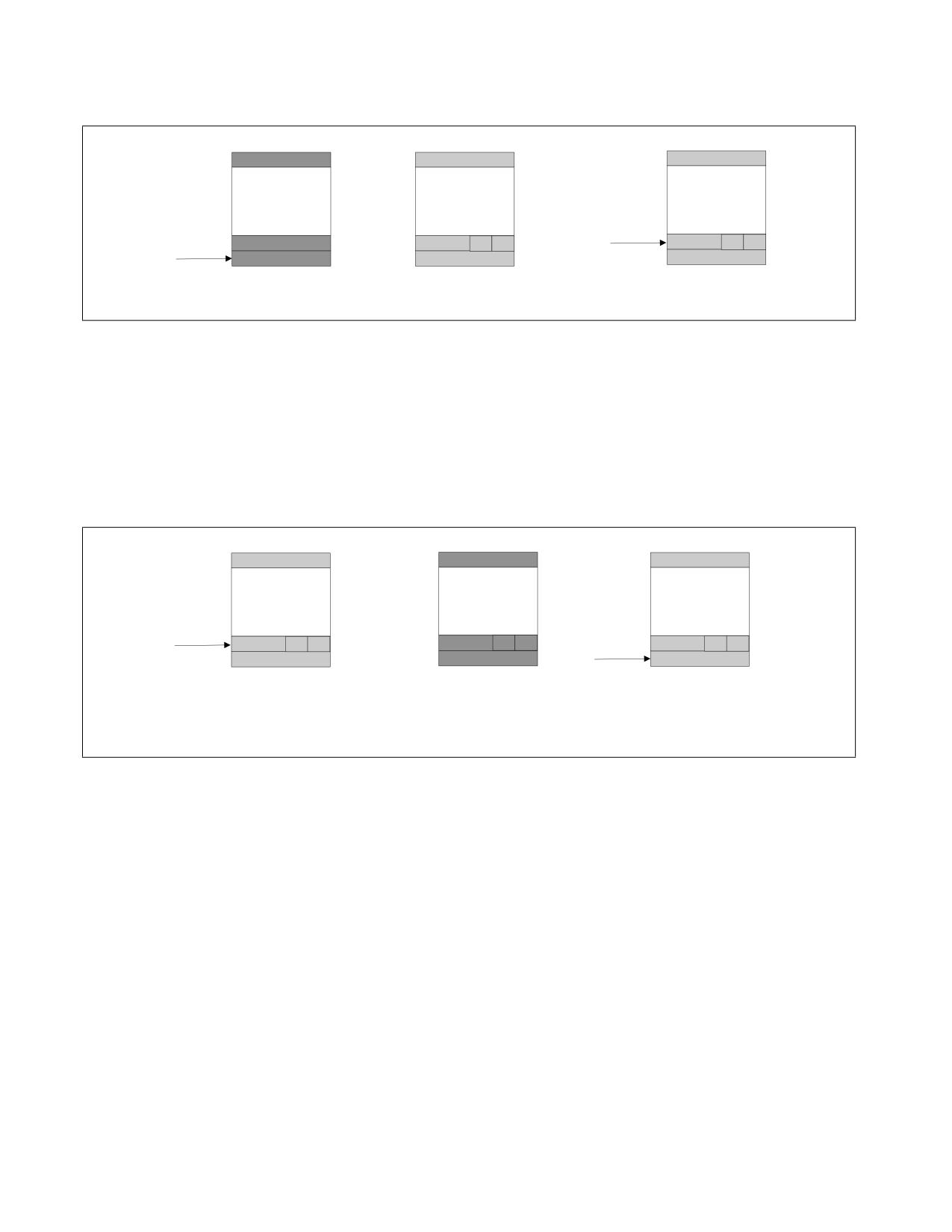
The following figure illustrates the RSTORSSP instruction operation during a shadow stack switching sequence.
Vol. 1
18-5
CONTROL-FLOW ENFORCEMENT TECHNOLOGY (CET)
New Shadow
Current
New Shadow
Stack to switch
Shadow Stack
Stack
to
FF8H
4000H
0
M
3FF8H
SSP
1000H
1
M
SSP
1000H
4000H
Current active shadow stack
Shadow stack to switch to
State following successful
RSTORSSP
Figure 18-2. RSTORSSP to Switch to New Shadow Stack
In this example, the initial SSP is 1000H and the shadow-stack-restore token is on a new shadow stack at address
3FF8H. The token at address 3FF8H holds the SSP when this restore point was created; in this example it is 4000H.
In order to switch to the new shadow stack, the RSTORSSP instruction is invoked with the memory operand
pointing set to 3FF8H. When the RSTORSSP instruction completes, the SSP is set to 3FF8H and the shadow-stack-
restore token at 3FF8H is replaced by a previous-ssp token that holds the address 1000H, i.e., the old SSP.
The following figure illustrates the SAVEPREVSSP instruction operation during a shadow stack switching sequence.
New Shadow
Previous
New Shadow
Stack
Shadow Stack
Stack
1000H
1
M
1000H
0
M
1000H
1
M
SSP
3FF8H
3FF8H
4000H
SSP
4000H
Current active shadow stack
“shadow stack restore” token
Current active shadow stack
with a “previous SSP” token
pushed on previous shadow
with a “previous SSP” token
stack following
popped off
SAVEPREVSSP
Figure 18-3. SAVEPREVSSP to Save a Restore Point
To allow switching back to this old shadow stack, a SAVEPREVSSP instruction is now invoked. The SAVEPREVSSP
instruction does not take any memory operand and expects to find a previous-ssp token at the top of the shadow
stack, i.e., at address 3FF8H. The SAVEPREVSSP instruction then saves a shadow-stack-restore token on the old
shadow stack at address FF8H, and the token itself holds the address 1000H which is the address recorded in the
previous-ssp token. The SAVEPREVSSP instruction also pops the previous-ssp token off the current shadow stack
and thus the SSP following SAVEPREVSSP is 4000H.
Subsequently to switch back to the old shadow stack, a RSTORSSP instruction may be invoked with memory
operand set to FF8H.
If, following a switch to a new shadow stack, it is not required to create a restore point on the old shadow stack,
then the previous-ssp token created by the RSTORSSP instruction can be popped off the shadow stack by using the
INCSSP instruction.
See the SAVEPREVSSP and RSTORSSP instruction operations for the detailed algorithm.
18-6
Vol. 1
CONTROL-FLOW ENFORCEMENT TECHNOLOGY (CET)
18.2.6 Constraining Execution at Targets of RET
Instructions at the target of a RET instruction will not execute, even speculatively, if the RET addresses (either from
normal stack or shadow stack) are speculative-only or do not match, unless the target of the RET is also predicted
(e.g., by a Return Stack Buffer prediction), when CET shadow stack is enabled. A RET address would be specula-
tive-only if it was modified by an older speculative-only store, or was an older value than the most recent value
stored to that address on the logical processor.
18.3
INDIRECT BRANCH TRACKING
When the indirect branch tracking feature is active, the indirect JMP/CALL instruction behavior changes as follows.
• JMP: If the next instruction retired after an indirect JMP is not an ENDBR32 instruction in legacy and compati-
bility mode, or ENDBR64 instruction in 64-bit mode, then a #CP fault is generated. Below JMP instructions are
tracked to enforce an ENDBRANCH. Note that Jcc, RIP relative, and far direct JMP are not included as these
have an offset encoded into the instruction and are not exploitable to create unintended control transfers.
- JMP r/m16, JMP r/m32, JMP r/m64
- JMP m16:16, JMP m16:32, JMP m16:64
• CALL: If the next instruction retired after an indirect CALL is not an ENDBR32 instruction in legacy and compat-
ibility mode, or ENDBR64 in 64-bit mode, then a #CP fault is generated. Below CALL instructions are tracked to
enforce an ENDBRANCH. Note that relative and zero displacement forms of CALL instructions are not included
as these have an offset encoded into the instruction and are not exploitable to create unintended control
transfers.
- CALL r/m16, CALL r/m32, CALL r/m64
- CALL m16:16, CALL m16:32, CALL m16:64
The ENDBR32 and ENDBR64 instructions will have the same effect as the NOP instruction on Intel 64 processors
that do not support CET. On processors supporting CET, these instructions do not change register or flag state. This
allows CET instrumented programs to execute on processors that do not support CET. Even when CET is supported
and enabled, these NOP-like instructions do not affect the execution state of the program, do not cause any addi-
tional register pressure, and are minimally intrusive from power and performance perspectives.
The processor implements two dual-state machines to track indirect CALL/JMP for terminations. One state machine
is maintained for user mode and one for supervisor mode. At reset the user and supervisor mode state machines
are in IDLE state.
On instructions other than indirect CALL/JMP, the state machine stays in the IDLE state.
On an indirect CALL or JMP instruction, the state machine transitions to the WAIT_FOR_ENDBRANCH state.
In the WAIT_FOR_ENDBRANCH state, the indirect branch tracking state machine verifies the next instruction is an
ENDBR32 instruction in legacy and compatibility mode, or ENDBR64 instruction in 64-bit mode, and either:
• Causes a #CP fault, or
• Allows the next instruction if legacy compatibility configuration allows (see Section 18.3.6).
The priority of the #CP(ENDBRANCH) exception relative to other events is as follows.
Vol. 1
18-7

CONTROL-FLOW ENFORCEMENT TECHNOLOGY (CET)
#CP Fault
Indirect CALL/JMP, RET
Target Instruction
Figure 18-4. Priority of Control Protection Exception on Missing ENDBRANCH
Higher priority faults/traps/events that occur at the end of an indirect CALL/JMP are delivered ahead of any
#CP(ENDBRANCH) fault. The CET state machine at the privilege level where the higher priority fault/trap/event
occurred retains its state when the control transfers to the fault/trap/event handler. The instruction pointer pushed
on the stack for a #CP(ENDBRANCH) fault is the address of the instruction at the target of the indirect CALL/JMP
that caused the fault.
18.3.1 No-track Prefix for Near Indirect CALL/JMP
CET allows software to designate certain indirect CALL and JMP instructions as “non-tracked indirect control
transfer instructions”. Software (e.g., compiler generated code for switch statements, jump tables, etc.) should use
the no-track prefix only if they have generated code to validate the possible targets of this CALL/JMP to be legal
targets. Software (e.g., compilers), when using the no-track prefix with CALL/JMP where an absolute offset is spec-
ified indirectly in a memory location, should ensure that such memory locations cannot be tampered. When
enabled by setting the NO_TRACK_EN control in the IA32_U_CET/IA32_S_CET MSR, near indirect CALL and JMP
instructions when prefixed with 3EH do not modify the CET indirect branch tracker. Far CALL and JMP instructions
are always tracked and ignore the 3EH prefix. When this control is 0, near indirect CALL and JMP instructions are
always tracked irrespective of the presence of the 3EH prefix.
In 64-bit mode, the 3EH prefix on an indirect CALL or JMP is recognized as a no-track prefix if there isn’t a 64H/65H
prefix on the instruction.
In legacy/compatibility mode, the 3EH prefix on an indirect CALL or JMP is recognized as a no-track prefix when it
is the last group 2 prefix on the instruction.
18-8
Vol. 1
CONTROL-FLOW ENFORCEMENT TECHNOLOGY (CET)
18.3.2 Terminology
The pseudocode for the instruction operations use a notation EndbranchEnabled(CPL) as a test of whether indirect
branch tracking is enabled at the CPL. This term returns a TRUE or FALSE indication as follows.
EndbranchEnabled(CPL):
IF CR4.CET = 1 AND CR0.PE = 1 AND EFLAGS.VM = 0
IF CPL = 3
THEN
(* Obtain the ENDBRANCH enable from MSR used to enable feature for CPL = 3 *)
ENDBR_ENABLED = IA32_U_CET.ENDBR_EN;
ELSE
(* Obtain the ENDBRANCH enable from MSR used to enable feature for CPL < 3 *)
ENDBR_ENABLED = IA32_S_CET.ENDBR_EN;
FI;
IF ENDBR_ENABLED = 1
THEN
return TRUE;
ELSE
return FALSE;
FI;
ELSE
(* Indirect branch tracking is not enabled in real mode and virtual-8086 mode or if the master CET feature
enable in CR4 is disabled *)
return FALSE;
ENDIF
Likewise the notation EndbranchEnabledAndNotSuppressed is defined as follows:
EndbranchEnabledAndNotSuppressed(CPL):
IF CR4.CET = 1 AND CR0.PE = 1 AND EFLAGS.VM = 0
IF CPL = 3
THEN
(* Obtain the ENDBRANCH enable from MSR used to enable feature for CPL = 3 *)
ENDBR_ENABLED = IA32_U_CET.ENDBR_EN;
SUPPRESSED = IA32_U_CET.SUPPRESS;
ELSE
(* Obtain the ENDBRANCH enable from MSR used to enable feature for CPL < 3 *)
ENDBR_ENABLED = IA32_S_CET.ENDBR_EN;
SUPPRESSED = IA32_S_CET.SUPPRESS;
FI;
IF ENDBR_ENABLED = 1 AND SUPPRESSED = 0
THEN
return TRUE;
ELSE
return FALSE;
FI;
ELSE
(* Indirect branch tracking is not enabled in real mode and virtual-8086 mode or if the master CET feature
enable in CR4 is disabled *)
return FALSE;
ENDIF
Vol. 1
18-9
CONTROL-FLOW ENFORCEMENT TECHNOLOGY (CET)
18.3.3 Indirect Branch Tracking
The hardware implements two CET indirect branch tracker state machines, one for user mode (CPL == 3) and one
for supervisor mode (CPL < 3). At any time, which of the CET indirect branch trackers is in the active state depends
on the CPL of the machine. When a user space program is executing, the CPL 3 CET indirect branch tracker is
active. When supervisor mode software is executing, the CPL < 3 tracker is active. This section describes the
various control transfer conditions and the tracker state on those transfers.
18.3.3.1 Control Transfers between CPL 3 and CPL < 3
Some events and instructions can cause control transfer to occur from CPL 3 to CPL < 3, and vice versa. As part of
the CPL change the hardware also switches the active CET indirect branch tracker. For example, when an interrupt
occurs during execution of a user mode (CPL == 3) program and it causes the CPL to switch to supervisor mode
(CPL < 3) then, as part of the CPL change, the user mode CET indirect branch tracker becomes inactive and the
supervisor mode CET indirect branch tracker becomes active. A subsequent IRET is used by the interrupt handler
to return to the interrupted user mode program. This IRET causes the processor to switch the CPL to user mode
(CPL ==3) and, as part of the CPL change, the supervisor mode CET indirect branch tracker becomes inactive and
the user mode CET indirect branch tracker becomes active.
The CPL where the event or instruction that caused the control transfer occurs is termed the source CPL, and the
CET indirect branch tracker state at that CPL is referred here as the source CET indirect branch tracker state. The
CPL reached at the end of the control transfer is termed the destination CPL, and the CET indirect branch tracker
state at that CPL is referred to as the destination CET indirect branch tracker state.
This section describes various cases of control transfers that occur between user mode (CPL 3) and supervisor
mode (CPL < 3).
In all these cases the source CET indirect branch tracker state becomes not active and retains its state (IDLE,
WAIT_FOR_ENDBRANCH), and the target CET indirect branch tracker state becomes active if there was no fault
during the transfer.
• Case 1: Far CALL/JMP, SYSCALL/SYSENTER
- If indirect branch tracking is enabled, the target indirect branch tracker state becomes active and is unsup-
pressed and goes to WAIT_FOR_ENDBRANCH. This enforces that the subroutine invoked by a far CALL/JMP
must begin with an ENDBRANCH.
• Case 2: Hardware interrupt/trap/exception/NMI/Software interrupt/Machine Checks
- If indirect branch tracking is enabled, the target indirect branch tracker state becomes active and is unsup-
pressed and goes to WAIT_FOR_ENDBRANCH.
• Case 3: IRET/Far RET
- If indirect branch tracking enabled, the target indirect branch tracker becomes active and keeps its state. If
the user mode was interrupted by a higher priority event, like an interrupt at the end of the indirect
CALL/JMP, then when an IRET or Far RET is used to return to the interrupted user mode program, the user
mode indirect branch tracker retains its state and a #CP fault will occur if the next instruction decoded is not
an ENDBR32/64 according to mode of machine.
18.3.3.2 Control Transfers within CPL 3 or CPL < 3
Some events and instructions can cause control transfer to occur within CPL 3 or CPL < 3. For such transfers since
the CPL class does not change, the same indirect branch tracker is used at the beginning and end of the control
transfer.
• Case 1: Far CALL/JMP, Near indirect CALL/JMPCALL/JMP
- Far CALL/JMP: If indirect branch tracking is enabled, active indirect branch tracker is unsuppressed and
goes to WAIT_FOR_ENDBRANCH.
- Near indirect CALL/JMPCALL/JMP: If indirect branch tracking is enabled and not suppressed, active indirect
branch tracker goes to WAIT_FOR_ENDBRANCH.
• Case 2: Hardware interrupt/trap/exception/NMI/Software interrupt/Machine Checks
18-10
Vol. 1

CONTROL-FLOW ENFORCEMENT TECHNOLOGY (CET)
- If indirect branch tracking is enabled, the active indirect branch tracker is unsuppressed and goes to
WAIT_FOR_ENDBRANCH.
• Case 3: IRET
- If indirect branch tracking is enabled, the active indirect branch tracker keeps its state.
18.3.4 Indirect Branch Tracking State Machine
The state machine is described by Table 18-1.
Table 18-1. Indirect Branch Tracking State Machine
Current State
Trigger
Next State
Instructions other than indirect CALL/JMP or
TRACKER=IDLE, SUPPRESS=0, END-
3EH prefixed near indirect CALL/JMP and
BR_EN=1
NO_TRACK_EN=1
TRACKER=IDLE, SUPPRESS=0, END-
Indirect CALL/JMP without 3EH prefix
BR_EN=1
Indirect CALL/JMP with 3EH prefix and
TRACKER=WAIT_FOR_ENDBRANCH, SUP-
NO_TRACK_EN=0
PRESS=0, ENDBR_EN=1
Far CALL/JMP
TRACKER= WAIT_FOR_ENDBRANCH, SUP-
INT3/INT1
PRESS=0, ENDBR_EN=1
TRACKER=IDLE, SUPPRESS=0, END-
ENDBRANCH instruction
BR_EN=1
TRACKER=IDLE, SUPPRESS=0, END-
Successful ENCLU[ERESUME]
BR_EN=1
If legacy compatibility treatment is not
TRACKER= WAIT_FOR_ENDBRANCH, SUP-
enabled or if not allowed by legacy code
PRESS=0, ENDBR_EN=1
page bitmap:
• No state change and deliver #CP
(ENDBRANCH)
Instructions other than ENDBRANCH, suc-
If legacy compatibility treatment is
cessful ENCLU[ERESUME] or INT3 or INT1
enabled and transfer allowed by legacy
code page bitmap:
• TRACKER=IDLE,
SUPRESS=!SUPPRESS_DIS,
ENDBR_EN=1
TRACKER=x, SUPPRESS=x, ENDBR_EN=0
All instructions
TRACKER=x, SUPPRESS=x, ENDBR_EN=0
TRACKER=WAIT_FOR_ENDBRANCH, SUP-
Far CALL/JMP, INTn/INT3/INTO
PRESS=0, ENDBR_EN=1
TRACKER=IDLE, SUPPRESS=1, END-
ENDBRANCH instruction
TRACKER=IDLE, SUPPRESS=0, END-
BR_EN=1
Successful ENCLU[ERESUME]
BR_EN=1
All other instructions including indirect
TRACKER=IDLE, SUPPRESS=1, END-
CALL/JMP
BR_EN=1
TRACKER=1, SUPPRESS=1, ENDBR_EN=1
(This state cannot be reached by hardware
NA
NA
and is disallowed as a valid state by
WRMSR/XRSTORS/VM entry/VM exit)
Vol. 1
18-11
CONTROL-FLOW ENFORCEMENT TECHNOLOGY (CET)
18.3.5 INT3 Treatment
INT3 are treated special in the WAIT_FOR_ENDBRANCH state. Occurrence of INT3 do not move the tracker to IDLE
but instead the #BP trap from the INT3 instructions respectively is delivered as a higher priority event than the #CP
exception due to missing ENDBRANCH.
Inside an enclave, INT3 delivers a fault-class exception and thus does not require the CPL to be less than DPL in the
IDT gate 3. Following opt-out entry, the instruction delivers #UD. Following opt-in entry, INT3 delivers #BP. The
special treatment of INT3 in WAIT_FOR_ENDBRANCH state does not apply in enclave mode following opt-out entry.
18.3.6 Legacy Compatibility Treatment
ENDBRANCH legacy compatibility treatment allows a CET enabled program to be used with legacy software that
was not compiled / instrumented with ENDBRANCH. A CET enabled program enters legacy compatibility treatment
when all of the below conditions are met.
1. Legacy compatibility configuration is enabled in this CPL class by setting the LEG_IW_EN bit in
IA32_U_CET/IA32_S_CET.
2. Control transfer is performed using an indirect CALL/JMP without no-track prefix to an instruction other than
ENDBRANCH.
3. The legacy code page bitmap is setup to indicate that the target of the control transfer is a legacy code page.
The legacy code page bitmap is a data structure in program memory that is used by the hardware to determine if
the code page to which a legacy transfer is being performed is allowed. The access rights for accessing the legacy
code page bitmap is determined by the current privilege level (CPL). The legacy code page bitmap is expected to
be setup as a read-only data structure.
When a matching ENDBRANCH instruction is not decoded at the target of an indirect CALL/JMP when required, the
processor performs the below actions.
CET indirect branch tracking state machine violation event handler:
If LEG_IW_EN == 1
LA = LIP;
IF ENCLAVE_MODE == 1
LA = LA - SECS.BASEADDR;
ENDIF
(* Load byte from bitmap. Address-size attribute for this load is 64 bits if IA32_EFER.LMA is 1 and is 32 bits when IA32_EFER.LMA
is 0 *)
IF (IA32_EFER.LMA & CS.L) == 0
BITMAP_BYTE = load 1 byte from address (BITMAP_BASE + LA[31:15])
ELSE IF (CR4.LA57 == 0)
BITMAP_BYTE = load 1 byte from address (BITMAP_BASE + LA[47:15])
ELSE
BITMAP_BYTE = load 1 byte from address (BITMAP_BASE + LA[56:15])
FI;
IF BITMAP_BYTE & (1 << LA[14:12]) == 0 then Deliver #CP(ENDBRANCH) fault
IF CPL = 3
IA32_U_CET.TRACKER = IDLE
IA32_U_CET.SUPPRESS = IA32_U_CET.SUPPRESS_DIS == 0 ? 1 : 0
ELSE
IA32_S_CET.TRACKER = IDLE
IA32_S_CET.SUPPRESS = IA32_S_CET.SUPPRESS_DIS == 0 ? 1 : 0
ENDIF
Restart the instruction (handle all arch. consistency around MOV SS state machines, STI etc.) without
opening up interrupt/trap window.
ELSE
Deliver #CP(ENDBRANCH) Fault
18-12
Vol. 1
CONTROL-FLOW ENFORCEMENT TECHNOLOGY (CET)
ENDIF
Faults/traps in pseudocode are delivered normally (e.g., #PF, EPT violation). On a fault, the active tracker holds the
last value (WAIT_FOR_ENDBRANCH) and the address saved on the stack is the current IP (instruction that wasn’t
the ENDBRANCH).
The CET indirect branch tracking state machine is suppressed in legacy compatibility mode if the SUPPRESS_DIS
control bit is 0.
Once the CET indirect branch tracking state machine has been suppressed, subsequent indirect CALL/JMP are not
tracked for termination instruction.
Once CET indirect branch tracking has been suppressed, subsequent execution of ENDBRANCH instructions will do
the following (see the ENDBR32 and ENDBR64 instructions in the Intel® 64 and IA-32 Architectures Software
Developer’s Manual, Volume 2A for details).
IF EndbranchEnabled(CPL) == 0
NOP
ELSE
SUPPRESS = 0
TRACKER = IDLE
ENDIF
18.3.6.1 Legacy Code Page Bitmap Format
The legacy code page bitmap is a flat bitmap whose linear address is pointed to by the EB_LEG_BITMAP_BASE.
Each bit in the bitmap represents a 4K page in linear memory. If the bit is 1 it indicates that the corresponding code
page is a legacy code page; else it is a CET-enabled code page.
The processor uses the linear address of the instruction to which legacy transfer was attempted to lookup the
bitmap. Bits of the linear address used as index in the bitmap are as follows.
• In legacy and compatibility mode: Bits 31:12.
• In 64-bit mode (EFER.LMA=1 and CS.L=1): Bits 47:12.
18.3.7 Other Considerations
18.3.7.1 Intel® Transactional Synchronization Extensions (Intel® TSX) Interactions
The XBEGIN instruction encodes the relative offset to the abort handler and hence the fallback to the abort handler
can be considered as a “direct” branch and the abort handler does not need to have an ENDBRANCH.
CET continues to enforce indirect CALL/JMP tracking within a transaction. Legacy compatibility treatment inside a
transaction functions normally. If a transaction abort occurs then the processor sets the state of the indirect branch
tracker to IDLE and not-suppressed.
18.3.7.2 #CP(ENDBRANCH) Priority w.r.t #NM and #UD
#NM, #UD and #CP(ENDBRANCH) are opcode based faults. However, #CP(ENDBRANCH) is in a higher priority
class than #NM and #UD as CET architecturally requires an ENDBRANCH at target of indirect CALL/JMP.
18.3.7.3 #CP(ENDBRANCH) Priority w.r.t #BP and #DB
Debug Exceptions priority is as follows.
• Traps delivered before any #CP(ENDBRANCH) fault: Data breakpoint trap, IO breakpoint trap single step trap,
task switch trap.
• Code Breakpoint fault detected before instruction decode and delivered before #CP(ENDBRANCH).
• General-detect (GD) exception condition fault: Lower priority than #CP(ENDBRANCH).
Vol. 1
18-13
CONTROL-FLOW ENFORCEMENT TECHNOLOGY (CET)
• On IRET back from #DB/#BP, the source indirect branch tracker becomes active if enabled and not suppressed.
INT3 does not cause #CP(ENDBRANCH) to support debugger usage of replacing bytes of ENDBRANCH with INT3 to
set breakpoints. INT3 at target of a CALL-JMP(indirect) cause #BP(INT3) instead of #CP(ENDBRANCH),
#CP(ENDBRANCH) fault is delayed. #BP caused by INT3 treated like other events that are higher priority than CET
fault. On IRET back from #BP the source indirect tracker becomes active if enabled and not suppressed.
18.3.8 Constraining Speculation after Missing ENDBRANCH
When the CET tracker is in the WAIT_FOR_ENDBRANCH state, instruction execution will be limited or blocked, even
speculatively, if the next instruction is not an ENDBRANCH.
This means that when indirect branch tracking is enabled and not suppressed, the instructions at the target of a
near indirect JMP/CALL without the no-track prefix will only speculatively execute if there is an ENDBRANCH at the
target. This can constrain both attacker controlled prediction as well as attacker controlled jump redirection attacks
on near indirect JMPs/CALLs by reducing the gadgets available to an attacker using these techniques. Early imple-
mentations of CET may limit the speculative execution to a small number of instructions (less than 8, with no more
than 5 loads) past a missing ENDBRANCH, while later implementations will completely block the speculative execu-
tion of instructions after a missing ENDBRANCH.
This mechanism also limits or blocks speculation of the next sequential instructions after an indirect JMP or CALL,
presuming the JMP/CALL puts the CET tracker into the WAIT_FOR_ENDBRANCH state and the next sequential
instruction is not an ENDBRANCH.
18.4
INTEL® TRUSTED EXECUTION TECHNOLOGY (INTEL® TXT) INTERACTIONS
GETSEC[ENTERACCS] and GETSEC[SENTER] clear CR4.CET, and it is not restored when these instructions
complete.
GETSEC[EXITAC] will cause #GP(0) fault if CR4.CET is set.
18-14
Vol. 1
CHAPTER 19
PROGRAMMING WITH INTEL® ADVANCED MATRIX EXTENSIONS
19.1
INTRODUCTION
Intel® Advanced Matrix Extensions (Intel® AMX) is a new 64-bit programming paradigm consisting of two compo-
nents: a set of 2-dimensional registers (tiles) representing sub-arrays from a larger 2-dimensional memory image,
and an accelerator able to operate on tiles, the first implementation is called TMUL (tile matrix multiply unit).
An Intel AMX implementation enumerates to the programmer how the tiles can be programmed by providing a
palette of options. Two palettes are supported; palette 0 represents the initialized state, and palette 1 consists of
8 KB of storage spread across 8 tile registers named TMM0..TMM7. Each tile has a maximum size of 16 rows x 64
bytes, (1 KB), however the programmer can configure each tile to smaller dimensions appropriate to their algo-
rithm. The tile dimensions supplied by the programmer (rows and bytes_per_row, i.e., colsb) are metadata that
drives the execution of tile and accelerator instructions. In this way, a single instruction can launch autonomous
multi-cycle execution in the tile and accelerator hardware. The palette value (palette_id) and metadata are held
internally in a tile related control register (TILECFG). The TILECFG contents will be commensurate with that
reported in the palette_table (see “CPUID-CPU Identification” in the Intel® 64 and IA-32 Architectures Software
Developer’s Manual, Volume 2A for a description of the available parameters).
Intel AMX is an extensible architecture. New accelerators can be added, or the TMUL accelerator may be enhanced
to provide higher performance. In these cases, the state (TILEDATA) provided by tiles may need to be made larger,
either in one of the metadata dimensions (more rows or colsb) and/or by supporting more tile registers (names).
The extensibility is carried out by adding new palette entries describing the additional state. Since execution is
driven through metadata, an existing Intel AMX binary could take advantage of larger storage sizes and higher
performance TMUL units by selecting the most powerful palette indicated by CPUID and adjusting loop and pointer
updates accordingly.
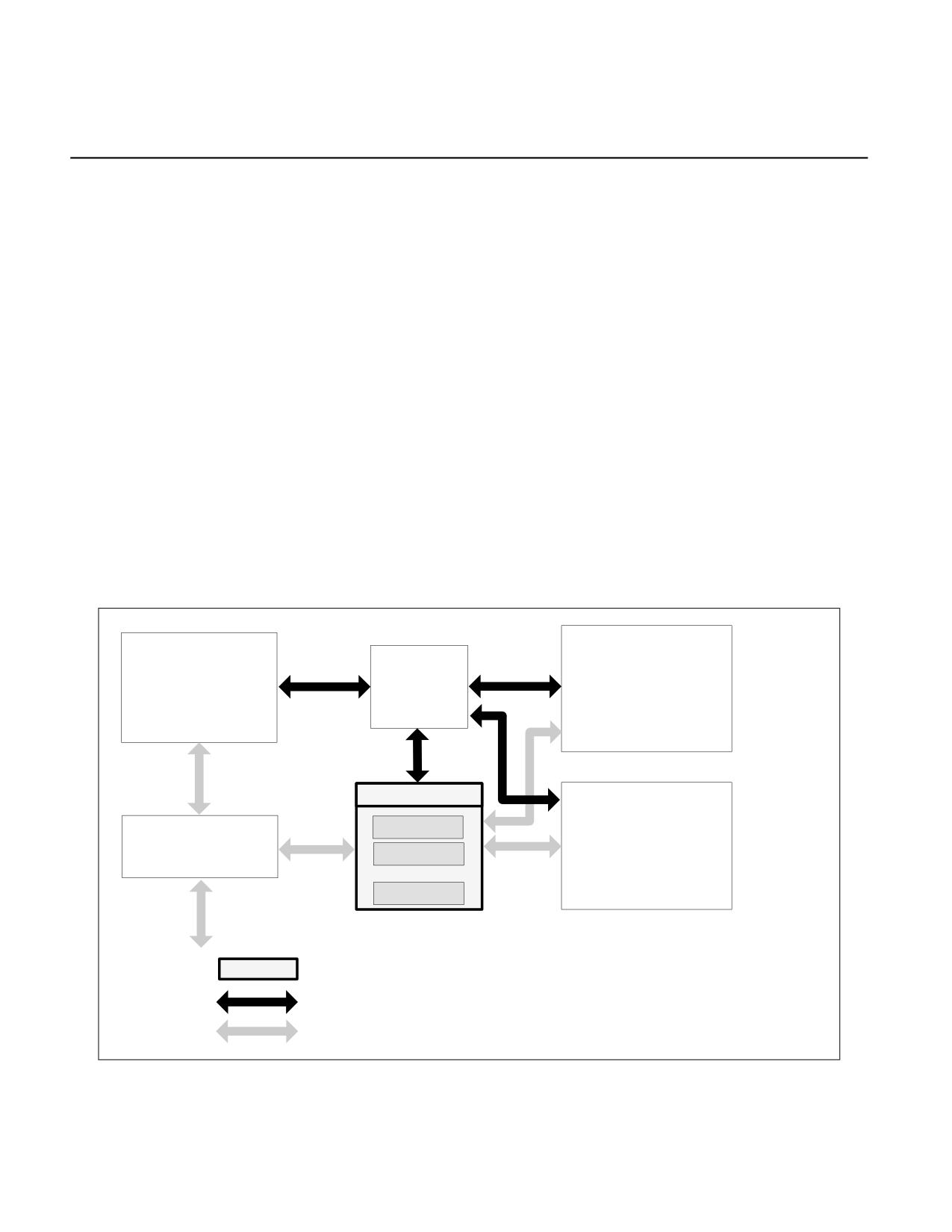
Tiles and
Accelerator 1 (TMUL)
IA Host
Accelerator
Commands
tmm0 += tmm1*tmm2
TILECFG
tmm0
Coherent Memory
Accelerator 2
Interface
tmm1
tmm[n-1]
New state to be managed by the OS.
Commands and status delivered synchronously via tile/accelerator instructions.
Dataflow; accelerators communicate to host through memory.
Figure 19-1. Intel® AMX Architecture
Vol. 1
19-1
PROGRAMMING WITH INTEL® ADVANCED MATRIX EXTENSIONS
Figure 19-1 shows a conceptual diagram of the Intel AMX architecture. An Intel architecture host drives the algo-
rithm, the memory blocking, loop indices and pointer arithmetic. Tile loads and stores and accelerator commands
are sent to multi-cycle execution units. Status, if required, is reported back. Intel AMX instructions are synchronous
in the Intel architecture instruction stream and the memory loaded and stored by the tile instructions is coherent
with respect to the host’s memory accesses. There are no restrictions on interleaving of Intel architecture and Intel
AMX code or restrictions on the resources the host can use in parallel with Intel AMX (e.g., Intel AVX-512). There is
also no architectural requirement on the Intel architecture compute capability of the Intel architecture host other
than it supports 64-bit mode.
Intel AMX instructions use new registers and inherit basic behavior from Intel architecture in the same manner that
Intel SSE and Intel AVX did. Tile instructions include loads and stores using the traditional Intel architecture
register set as pointers. The TMUL instruction set (defined to be CPUID bits AMX_BF16 and AMX_INT8) only
supports reg-reg operations.
TILECFG is programmed using the LDTILECFG instruction. The selected palette defines the available storage and
general configuration while the rest of the memory data specifies the number of rows and column bytes for each
tile. Consistency checks are performed to ensure the TILECFG matches the restrictions of the palette. A General
Protection fault (#GP) is reported if the LDTILECFG fails consistency checks. A successful load of
TILECFG with a palette_id other than 0 is represented in this document with TILES_CONFIGURED = 1. When the
TILECFG is initialized (palette_id = 0), it is represented in the document as TILES_CONFIGURED = 0. Nearly all
Intel AMX instructions will generate a #UD exception if TILES_CONFIGURED is not equal to 1; the exceptions are
those that do TILECFG maintenance: LDTILECFG, STTILECFG, and TILERELEASE.
If a tile is configured to contain M rows by N column bytes, LDTILECFG will ensure that the metadata values are
appropriate to the palette (e.g., that M ≤ 16 and N ≤ 64 for palette 1). The four M and N values can all be different
as long as they adhere to the restrictions of the palette. Further dynamic checks are done in the tile and the TMUL
instruction set to deal with cases where a legally configured tile may be inappropriate for the instruction operation.
Tile registers can be set to ‘invalid’ by configuring the rows and colsb to ‘0’.
Tile loads and stores are strided accesses from the application memory to packed rows of data. Algorithms are
expressed assuming row major data layout. Column major users should translate the terms according to their
orientation.
TILELOAD* and TILESTORE* instructions are restartable and can handle (up to) 2*rows page faults per instruction.
Restartability is provided by a start_row parameter in the TILECFG register.
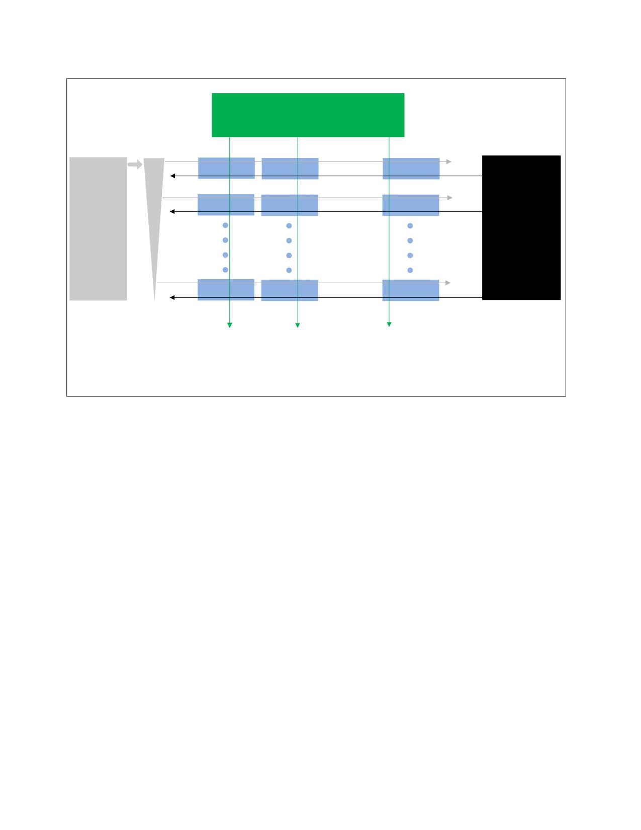
The TMUL unit is conceptually a grid of fused multiply-add units able to read and write tiles. The dimensions of the
TMUL unit (tmul_maxk and tmul_maxn) are enumerated similar to the maximum dimensions of the tiles (see
“CPUID-CPU Identification” in the Intel® 64 and IA-32 Architectures Software Developer’s Manual, Volume 2A for
details).
The matrix multiplications in the TMUL instruction set compute C[M][N] += A[M][K] * B[K][N]. The M, N, and K
values will cause the TMUL instruction set to generate a #UD exception if the dimensions do not match for matrix
multiply or do not match the palette.
In Figure 19-2, the number of rows in tile B matches the K dimension in the matrix multiplication pseudocode. K
dimensions smaller than that enumerated in the TMUL grid are also possible and any additional computation the
TMUL unit can support will not affect the result.
The number of elements specified by colsb of the B matrix is also less than or equal to tmul_maxn. Any remaining
values beyond that specified by the metadata will be set to zero.
19-2
Vol. 1
PROGRAMMING WITH INTEL® ADVANCED MATRIX EXTENSIONS
C[M][N]
C[m][0]
C[m][1]
C[m][n-1]
A[m][0]
FMA.
0.0
FMA.0
.1
FMA.0.N-1
B[0][:N]
A[m-1][1]
FMA.
1.0
FMA.1.1
FMA.1.N-1
B[1][:N]
A[M][K]
B[K][N]
A[m-K+1][K-1]
FMA.K
-1.0
FMA.K-1.1
FMA.K-1.N-1
B[K-1][:N]
C[m-K+1][0]
C[m-K+1][1]
C[m-K+1][n-1]
for m < M:
// time steps
for k < K:
// grid height
for n < N:
// SIMD dimension
C[m][n] += VNNI_MUL(A[m][k], B[k][n])
Figure 19-2. The TMUL Unit
The XSAVE feature set supports context management of the new state defined for Intel AMX. This support is
described in Section 19.2.
19.1.1 Tile Architecture Details
The supported parameters for the tile architecture are reported via CPUID; this includes information about how the
number of tile registers (max_names) can be configured (the palette). Configuring the tile architecture is intended
to be done once when entering a region of tile code using the LDTILECFG instruction specifying the selected palette
and describing in detail the configuration for each tile. Incorrect assignments will result in a General Protection fault
(#GP). Successful LDTILECFG initializes (zeroes) TILEDATA.
Exiting a tile region is done with the TILERELEASE instruction. It takes no parameters and invalidates all tiles (indi-
cating that the data no longer needs any saving or restoring). Essentially, it is an optimization of LDTILECFG with
an implicit palette of 0.
For applications that execute consecutive Intel AMX regions with differing configurations, TILERELEASE is not
required between them since the second LDTILECFG will clear all the data while loading the new configuration.
There is no instruction set support for automatic nesting of tile regions, though with sufficient effort software can
accomplish this by saving and restoring TILEDATA and TILECFG either through the XSAVE architecture or the Intel
AMX instructions.
The tile architecture boots in its INIT state, with TILECFG and TILEDATA set to zero. A successfully executing LDTI-
LECFG instruction to a non-zero palette sets the TILES_CONFIGURED=1, indicating the TILECFG is not in the INIT
state. The TILERELEASE instruction sets TILES_CONFIGURED = 0 and initializes (zeroes) TILEDATA.
To facilitate handling of tile configuration data, there is a STTILECFG instruction. If the tile configuration is in the
INIT state (TILES_CONFIGURED == 0), then STTILECFG will write 64 bytes of zeros. Otherwise STTILECFG will
store the TILECFG to memory in the format used by LDTILECFG.
Vol. 1
19-3
PROGRAMMING WITH INTEL® ADVANCED MATRIX EXTENSIONS
19.1.2 TMUL Architecture Details
The supported parameters for the TMUL architecture are reported via CPUID; see “CPUID-CPU Identification” in
the Intel® 64 and IA-32 Architectures Software Developer’s Manual, Volume 2A, for details. These parameters
include a maximum height (tmul_maxk) and a maximum SIMD dimension (tmul_maxn). The metadata that
accompanies the srcdest, src1, and src2 tiles to the TMUL unit will be dynamically checked to see that they match
the TMUL unit support for the data type and match the requirements of a meaningful matrix multiplication.
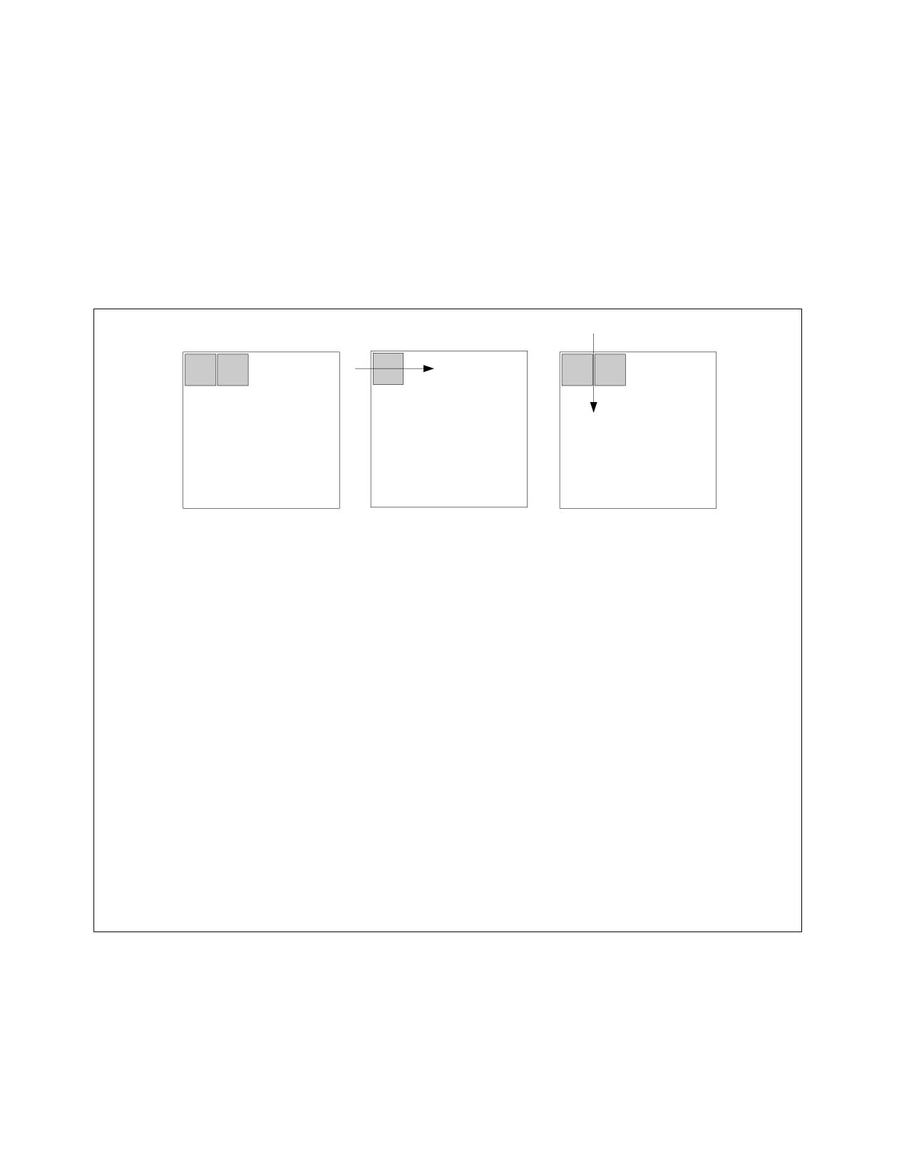
Figure 19-3 shows an example of the inner loop of an algorithm of using the TMUL architecture to compute a matrix
multiplication. In this example, we use two result tiles, tmm0 and tmm1, from matrix C to accumulate the interme-
diate results. One tile from the A matrix (tmm2) is re-used twice as we multiply it by two tiles from the B matrix.
The algorithm then advances pointers to load a new A tile and two new B tiles from the directions indicated by the
arrows. An outer loop, not shown, adjusts the pointers for the C tiles.
C
A
B
LDTILECFG [rax]
// assume some outer loops driving the cache tiling (not shown)
{
TILELOADD tmm0, [rsi+rdi]
// srcdst, RSI points to C, RDI is strided value
TILELOADD tmm1, [rsi+rdi+N]
// second tile of C, unrolling in SIMD dimension N
MOV r14, 0
LOOP:
TILELOADD tmm2, [r8+r9]
// src2 is strided load of A, reused for 2 TMUL instr.
TILELOADD tmm3, [r10+r11]
// src1 is strided load of B
TDPBUSD tmm0, tmm2, tmm3 // update left tile of C
TILELOADD tmm3, [r10+r11+N]
// src1 loaded with B from next rightmost tile
TDPBUSD tmm1, tmm2, tmm3 // update right tile of C
ADD r8, K
// update pointers by constants known outside of loop
ADD r10, K*r11
ADD r14, K
CMP r14, LIMIT
JNE LOOP
TILESTORED [rsi+rdi], tmm0 // update the C matrix in memory
TILESTORED [rsi+rdi+M], tmm1
} // end of outer loop
TILERELEASE
// return tiles to INIT state
Figure 19-3. Matrix Multiply C+= A*B
19.1.3 Handling of Tile Row and Column Limits
Intel AMX operations will zero any rows and any columns beyond the dimensions specified by TILECFG. Tile opera-
tions will zero the data beyond the configured number of column bytes as each row is written. For example, with
64-byte rows and a tile configured with 10 rows and 48 columns, an operation writing dword elements would write
19-4
Vol. 1
PROGRAMMING WITH INTEL® ADVANCED MATRIX EXTENSIONS
each of the first 10 rows with 48 bytes of output/result data and zero the remaining 16 bytes in each row. Tile oper-
ations also fully zero any rows after the first 10 configured rows. When using a 1 KByte tile with 64-byte rows,
there would be 16 rows, so in this example, the last 6 rows would also be zeroed.
Intel AMX instructions will always obey the metadata on reads and the zeroing rules on writes, and so a subsequent
XSAVE would see zeros in the appropriate locations. Tiles that are not written by Intel AMX instructions between
XRSTOR and XSAVE will write back with the same image they were loaded with regardless of the value of TILECFG.
19.1.4 Exceptions and Interrupts
Tile instructions are restartable so that operations that access strided memory can restart after page faults. To
support restarting instructions after these events, the instructions store information in the TILECFG.start_row
register. TILECFG.start_row indicates the row that should be used for restart; i.e., it indicates next row after the
rows that have already been successfully loaded (on a TILELOAD) or written to memory (on a TILESTORE) and
prevents repeating work that was successfully done.
The TMUL instruction set is not sensitive to the TILECFG.start_row value; this is due to there not being TMUL
instructions with memory operands or any restartable faults.
19.2
RECOMMENDATIONS FOR SYSTEM SOFTWARE
Intel AMX is an XSAVE-enabled feature, meaning that it requires use of the XSAVE feature set for their enabling.
Specifically, Intel AMX instructions and state are available only if system software has set CR4.OSXSAVE and also
set XCR0[18:17] to 11B. In addition, use of Intel AMX instructions is disabled if system software has used extended
feature disable (XFD) and set either IA32_XFD[17] or IA32_XFD[18] to 1. See Chapter 13, “Managing State Using
the XSAVE Feature Set,” for more details.
NOTE
The first processors implementing Intel AMX will support setting IA32_XFD[18] but not
IA32_XFD[17].
Once Intel AMX has been enabled, system software can disable it by clearing XCR0[18:17], by clearing
CR4.OSXSAVE, or by setting either IA32_XFD[17] or IA32_XFD[18]. Before doing so, system software should first
initialize AMX state (e.g., by executing TILERELEASE); maintaining AMX state in a non-initialized state may have
negative power and performance implications and will prevent the execution of In-Field Scan tests. In addition,
software should not rely on the state of the tile data after setting IA32_XFD[17] or IA32_XFD[18]; software should
always reload or reinitialize the tile data after clearing IA32_XFD[17] and IA32_XFD[18].
System software should not use XFD to implement a “lazy restore” approach to management of the TILEDATA state
component. This approach will not operate correctly for a variety of reasons. One is that the LDTILECFG and
TILERELEASE instructions initialize TILEDATA and do not cause an #NM exception. Another is that an execution of
XSAVE, XSAVEC, XSAVEOPT, or XSAVES by a user thread will save TILEDATA as initialized instead of the data
expected by the user thread.
19.3
IMPLEMENTATION PARAMETERS
The parameters are reported via CPUID leaf 1DH. Index 0 reports all zeros for all fields.
Vol. 1
19-5
PROGRAMMING WITH INTEL® ADVANCED MATRIX EXTENSIONS
define palette_table[id]:
uint16_t total_tile_bytes
uint16_t bytes_per_tile
uint16_t bytes_per_row
uint16_t max_names
uint16_t max_rows
The tile parameters are set by LDTILECFG or XRSTOR* of TILECFG:
define tile[tid]:
byte rows
word colsb // bytes_per_row
bool valid
19.4
HELPER FUNCTIONS
The helper functions used in Intel AMX instructions are defined below.
define write_row_and_zero(treg, r, data, nbytes):
for j in 0 ... nbytes-1:
treg.row[r].byte[j] := data.byte[j]
// zero the rest of the row
for j in nbytes ... palette_table[tilecfg.palette_id].bytes_per_row-1:
treg.row[r].byte[j] := 0
define zero_upper_rows(treg, r):
for i in r ... palette_table[tilecfg.palette_id].max_rows-1:
for j in 0 ... palette_table[tilecfg.palette_id].bytes_per_row-1:
treg.row[i].byte[j] := 0
define zero_tilecfg_start():
tilecfg.start_row := 0
define zero_all_tile_data():
if XCR0[TILEDATA]:
b := CPUID.0DH.TILEDATA:EAX // size of feature
for j in 0 ... b:
TILEDATA.byte[j] := 0
19-6
Vol. 1
PROGRAMMING WITH INTEL® ADVANCED MATRIX EXTENSIONS
define xcr0_supports_palette(palette_id):
if palette_id == 0:
return 1
elif palette_id == 1:
if XCR0[TILECFG] and XCR0[TILEDATA]:
return 1
return 0
Vol. 1
19-7
PROGRAMMING WITH INTEL® ADVANCED MATRIX EXTENSIONS
19-8
Vol. 1
CHAPTER 20
INPUT/OUTPUT
In addition to transferring data to and from external memory, IA-32 processors can also transfer data to and from
input/output ports (I/O ports). I/O ports are created in system hardware by circuity that decodes the control, data,
and address pins on the processor. These I/O ports are then configured to communicate with peripheral devices. An
I/O port can be an input port, an output port, or a bidirectional port. Some I/O ports are used for transmitting data,
such as to and from the transmit and receive registers, respectively, of a serial interface device. Other I/O ports are
used to control peripheral devices, such as the control registers of a disk controller.
This chapter describes the processor’s I/O architecture. The topics discussed include:
• I/O port addressing.
• I/O instructions.
• I/O protection mechanism.
20.1
I/O PORT ADDRESSING
The processor permits applications to access I/O ports in either of two ways:
• Through a separate I/O address space.
• Through memory-mapped I/O.
Accessing I/O ports through the I/O address space is handled through a set of I/O instructions and a special I/O
protection mechanism. Accessing I/O ports through memory-mapped I/O is handled with the processor’s general-
purpose move and string instructions, with protection provided through segmentation or paging. I/O ports can be
mapped so that they appear in the I/O address space or the physical-memory address space (memory mapped
I/O) or both.
One benefit of using the I/O address space is that writes to I/O ports are guaranteed to be completed before the
next instruction in the instruction stream is executed. Thus, I/O writes to control system hardware cause the hard-
ware to be set to its new state before any other instructions are executed. See Section 20.6, “Ordering I/O,” for
more information on serializing of I/O operations.
20.2
I/O PORT HARDWARE
From a hardware point of view, I/O addressing is handled through the processor’s address lines. For the P6 family,
Pentium 4, and Intel Xeon processors, the request command lines signal whether the address lines are being driven
with a memory address or an I/O address; for Pentium processors and earlier IA-32 processors, the M/IO# pin indi-
cates a memory address (1) or an I/O address (0). When the separate I/O address space is selected, it is the
responsibility of the hardware to decode the memory-I/O bus transaction to select I/O ports rather than memory.
Data is transmitted between the processor and an I/O device through the data lines.
20.3
I/O ADDRESS SPACE
The processor’s I/O address space is separate and distinct from the physical-memory address space. The I/O
address space consists of 216 (64K) individually addressable 8-bit I/O ports, numbered 0 through FFFFH. I/O port
addresses 0F8H through 0FFH are reserved. Do not assign I/O ports to these addresses. The result of an attempt
to address beyond the I/O address space limit of FFFFH is implementation-specific; see the Developer’s Manuals for
specific processors for more details.
Any two consecutive 8-bit ports can be treated as a 16-bit port, and any four consecutive ports can be a 32-bit port.
In this manner, the processor can transfer 8, 16, or 32 bits to or from a device in the I/O address space. Like words
in memory, 16-bit ports should be aligned to even addresses (0, 2, 4, ...) so that all 16 bits can be transferred in a
Vol. 1
20-1

INPUT/OUTPUT
single bus cycle. Likewise, 32-bit ports should be aligned to addresses that are multiples of four (0, 4, 8, ...). The
processor supports data transfers to unaligned ports, but there is a performance penalty because one or more
extra bus cycle must be used.
The exact order of bus cycles used to access unaligned ports is undefined and is not guaranteed to remain the same
in future IA-32 processors. If hardware or software requires that I/O ports be written to in a particular order, that
order must be specified explicitly. For example, to load a word-length I/O port at address 2H and then another word
port at 4H, two word-length writes must be used, rather than a single doubleword write at 2H.
Note that the processor does not mask parity errors for bus cycles to the I/O address space. Accessing I/O ports
through the I/O address space is thus a possible source of parity errors.
20.3.1 Memory-Mapped I/O
I/O devices that respond like memory components can be accessed through the processor’s physical-memory
address space (see Figure 20-1). When using memory-mapped I/O, any of the processor’s instructions that refer-
ence memory can be used to access an I/O port located at a physical-memory address. For example, the MOV
instruction can transfer data between any register and a memory-mapped I/O port. The AND, OR, and TEST
instructions may be used to manipulate bits in the control and status registers of a memory-mapped peripheral
device.
Certain instructions may take an exception or VM exit after completing a memory access (either a read or a write)
to a memory-mapped I/O address. This exception or VM exit could be due to the instruction performing multiple
memory accesses (e.g., MOVS, PUSH mem, POP mem, PUSHAD, etc.) or could be due to the ordering of exceptions
or VM exits within the instruction (e.g., a DIV mem that takes a #DE or a CALL that causes a task switch VM exit).
If software later re-executes that instruction (e.g., after an IRET or VMRESUME), the MMIO (memory-mapped I/O)
access may occur again. If the memory-mapped I/O access has a side-effect, that side-effect may be executed
each time the memory-mapped I/O access occurs. If that is problematic, software must ensure that exceptions or
VM exits do not occur after accessing the MMIO.
When using memory-mapped I/O, caching of the address space mapped for I/O operations must be prevented.
With the Pentium 4, Intel Xeon, and P6 family processors, caching of I/O accesses can be prevented by using
memory type range registers (MTRRs) to map the address space used for the memory-mapped I/O as uncacheable
(UC). See Chapter 14, “Memory Cache Control,” in the Intel® 64 and IA-32 Architectures Software Developer’s
Manual, Volume 3A, for a complete discussion of the MTRRs.
The Pentium and Intel486 processors do not support MTRRs. Instead, they provide the KEN# pin, which when held
inactive (high) prevents caching of all addresses sent out on the system bus. To use this pin, external address
decoding logic is required to block caching in specific address spaces.
Physical Memory
FFFF
EPROM
I/O Port
I/O Port
I/O Port
RAM
0
Figure 20-1. Memory-Mapped I/O
20-2
Vol. 1
INPUT/OUTPUT
All the IA-32 processors that have on-chip caches also provide the PCD (page-level cache disable) flag in page table
and page directory entries. This flag allows caching to be disabled on a page-by-page basis. See “Page-Directory
and Page-Table Entries” in Chapter 4 of the Intel® 64 and IA-32 Architectures Software Developer’s Manual,
Volume 3A.
20.4
I/O INSTRUCTIONS
The processor’s I/O instructions provide access to I/O ports through the I/O address space. (These instructions
cannot be used to access memory-mapped I/O ports.) There are two groups of I/O instructions:
• Those that transfer a single item (byte, word, or doubleword) between an I/O port and a general-purpose
register.
• Those that transfer strings of items (strings of bytes, words, or doublewords) between an I/O port and
memory.
The register I/O instructions IN (input from I/O port) and OUT (output to I/O port) move data between I/O ports
and the EAX register (32-bit I/O), the AX register (16-bit I/O), or the AL (8-bit I/O) register. The address of the I/O
port can be given with an immediate value or a value in the DX register.
The string I/O instructions INS (input string from I/O port) and OUTS (output string to I/O port) move data
between an I/O port and a memory location. The address of the I/O port being accessed is given in the DX register;
the source or destination memory address is given in the DS:ESI or ES:EDI register, respectively.
When used with the repeat prefix REP, the INS and OUTS instructions perform string (or block) input or output
operations. The repeat prefix REP modifies the INS and OUTS instructions to transfer blocks of data between an I/O
port and memory. Here, the ESI or EDI register is incremented or decremented (according to the setting of the DF
flag in the EFLAGS register) after each byte, word, or doubleword is transferred between the selected I/O port and
memory.
See the references for IN, INS, OUT, and OUTS in Chapter 3 and Chapter 4 of the Intel® 64 and IA-32 Architectures
Software Developer’s Manual, Volumes 2A, 2B, 2C, & 2D, for more information on these instructions.
20.5
PROTECTED-MODE I/O
When the processor is running in protected mode, the following protection mechanisms regulate access to I/O
ports:
• When accessing I/O ports through the I/O address space, two protection devices control access:
- The I/O privilege level (IOPL) field in the EFLAGS register.
- The I/O permission bit map of a task state segment (TSS).
• When accessing memory-mapped I/O ports, the normal segmentation and paging protection and the MTRRs
(in processors that support them) also affect access to I/O ports. See Chapter 6, “Protection,” and Chapter 14,
“Memory Cache Control,” in the Intel® 64 and IA-32 Architectures Software Developer’s Manual, Volume 3A, for
a complete discussion of memory protection.
The following sections describe the protection mechanisms available when accessing I/O ports in the I/O address
space with the I/O instructions.
20.5.1 I/O Privilege Level
In systems where I/O protection is used, the IOPL field in the EFLAGS register controls access to the I/O address
space by restricting use of selected instructions. This protection mechanism permits the operating system or exec-
utive to set the privilege level needed to perform I/O. In a typical protection ring model, access to the I/O address
space is restricted to privilege levels 0 and 1. Here, the kernel and the device drivers are allowed to perform I/O,
while less privileged device drivers and application programs are denied access to the I/O address space. Applica-
tion programs must then make calls to the operating system to perform I/O.
Vol. 1
20-3
INPUT/OUTPUT
The following instructions can be executed only if the current privilege level (CPL) of the program or task currently
executing is less than or equal to the IOPL: IN, INS, OUT, OUTS, CLI (clear interrupt-enable flag), and STI (set
interrupt-enable flag). These instructions are called I/O sensitive instructions, because they are sensitive to the
IOPL field. Any attempt by a less privileged program or task to use an I/O sensitive instruction results in a general-
protection exception (#GP) being signaled. Because each task has its own copy of the EFLAGS register, each task
can have a different IOPL.
The I/O permission bit map in the TSS can be used to modify the effect of the IOPL on I/O sensitive instructions,
allowing access to some I/O ports by less privileged programs or tasks (see Section 20.5.2, “I/O Permission Bit
Map”).
A program or task can change its IOPL only with the POPF and IRET instructions; however, such changes are privi-
leged. No procedure may change the current IOPL unless it is running at privilege level 0. An attempt by a less priv-
ileged procedure to change the IOPL does not result in an exception; the IOPL simply remains unchanged.
The POPF instruction also may be used to change the state of the IF flag (as can the CLI and STI instructions);
however, the POPF instruction in this case is also I/O sensitive. A procedure may use the POPF instruction to change
the setting of the IF flag only if the CPL is less than or equal to the current IOPL. An attempt by a less privileged
procedure to change the IF flag does not result in an exception; the IF flag simply remains unchanged.
20.5.2 I/O Permission Bit Map
The I/O permission bit map is a device for permitting limited access to I/O ports by less privileged programs or
tasks and for tasks operating in virtual-8086 mode. The I/O permission bit map is located in the TSS (see
Figure 20-2) for the currently running task or program. The address of the first byte of the I/O permission bit map
is given in the I/O map base address field of the TSS. The size of the I/O permission bit map and its location in the
TSS are variable.
Task State Segment (TSS)
31
24 23
0
Last byte of
1
1
1
1
1
1
1
1
bitmap must be
followed by a
byte with all
I/O Permission Bit Map
bits set.
I/O map base
I/O Map Base
64H
must not
exceed DFFFH.
0
Figure 20-2. I/O Permission Bit Map
Because each task has its own TSS, each task has its own I/O permission bit map. Access to individual I/O ports
can thus be granted to individual tasks.
If in protected mode and the CPL is less than or equal to the current IOPL, the processor allows all I/O operations
to proceed. If the CPL is greater than the IOPL or if the processor is operating in virtual-8086 mode, the processor
checks the I/O permission bit map to determine if access to a particular I/O port is allowed. Each bit in the map
corresponds to an I/O port byte address. For example, the control bit for I/O port address 29H in the I/O address
space is found at bit position 1 of the sixth byte in the bit map. Before granting I/O access, the processor tests all
the bits corresponding to the I/O port being addressed. For a doubleword access, for example, the processors tests
the four bits corresponding to the four adjacent 8-bit port addresses. If any tested bit is set, a general-protection
exception (#GP) is signaled. If all tested bits are clear, the I/O operation is allowed to proceed.
20-4
Vol. 1
INPUT/OUTPUT
Because I/O port addresses are not necessarily aligned to word and doubleword boundaries, the processor reads
two bytes from the I/O permission bit map for every access to an I/O port. To prevent exceptions from being
generated when the ports with the highest addresses are accessed, an extra byte needs to be included in the TSS
immediately after the table. This byte must have all of its bits set, and it must be within the segment limit.
It is not necessary for the I/O permission bit map to represent all the I/O addresses. I/O addresses not spanned by
the map are treated as if they had set bits in the map. For example, if the TSS segment limit is 10 bytes past the
bit-map base address, the map has 11 bytes and the first 80 I/O ports are mapped. Higher addresses in the I/O
address space generate exceptions.
If the I/O bit map base address is greater than or equal to the TSS segment limit, there is no I/O permission map,
and all I/O instructions generate exceptions when the CPL is greater than the current IOPL.
20.6
ORDERING I/O
When controlling I/O devices it is often important that memory and I/O operations be carried out in precisely the
order programmed. For example, a program may write a command to an I/O port, then read the status of the I/O
device from another I/O port. It is important that the status returned be the status of the device after it receives
the command, not before.
When using memory-mapped I/O, caution should be taken to avoid situations in which the programmed order is
not preserved by the processor. To optimize performance, the processor allows cacheable memory reads to be
reordered ahead of buffered writes in most situations. Internally, processor reads (cache hits) can be reordered
around buffered writes. When using memory-mapped I/O, therefore, it is possible that an I/O read might be
performed before the memory write of a previous instruction. The recommended method of enforcing program
ordering of memory-mapped I/O accesses with the Pentium 4, Intel Xeon, and P6 family processors is to use the
MTRRs to make the memory mapped I/O address space uncacheable; for the Pentium and Intel486 processors,
either the KEN# pin or the PCD flags can be used for this purpose (see Section 20.3.1, “Memory-Mapped I/O”).
When the target of a read or write is in an uncacheable region of memory, memory reordering does not occur
externally at the processor’s pins (that is, reads and writes appear in-order). Designating a memory mapped I/O
region of the address space as uncacheable ensures that reads and writes of I/O devices are carried out in program
order. See Chapter 14, “Memory Cache Control,” in the Intel® 64 and IA-32 Architectures Software Developer’s
Manual, Volume 3A, for more information on using MTRRs.
Another method of enforcing program order is to insert one of the serializing instructions, such as the CPUID
instruction, between operations. See Chapter 11, “Multiple-Processor Management,” in the Intel® 64 and IA-32
Architectures Software Developer’s Manual, Volume 3A, for more information on serialization of instructions.
It should be noted that the chipset being used to support the processor (bus controller, memory controller, and/or
I/O controller) may post writes to uncacheable memory which can lead to out-of-order execution of memory
accesses. In situations where out-of-order processing of memory accesses by the chipset can potentially cause
faulty memory-mapped I/O processing, code must be written to force synchronization and ordering of I/O opera-
tions. Serializing instructions can often be used for this purpose.
When the I/O address space is used instead of memory-mapped I/O, the situation is different in two respects:
• The processor never buffers I/O writes. Therefore, strict ordering of I/O operations is enforced by the
processor. (As with memory-mapped I/O, it is possible for a chipset to post writes in certain I/O ranges.)
• The processor synchronizes I/O instruction execution with external bus activity (see Table 20-1).
Vol. 1
20-5

INPUT/OUTPUT
Table 20-1. I/O Instruction Serialization
Processor Delays Execution of …
Until Completion of …
Instruction Being
Executed
Current Instruction?
Next Instruction?
Pending Stores?
Current Store?
IN
Yes
Yes
INS
Yes
Yes
REP INS
Yes
Yes
OUT
Yes
Yes
Yes
OUTS
Yes
Yes
Yes
REP OUTS
Yes
Yes
Yes
20-6
Vol. 1
CHAPTER 21
PROCESSOR IDENTIFICATION AND FEATURE DETERMINATION
When writing software intended to run on Intel processors, it is necessary to identify the type of processor present
in a system and the processor features that are available to an application.
The CPUID instruction, known as CPU Identification, was introduced with the Intel® Pentium processor to query the
processor’s information name space for its identity and supported features. Logically, the CPUID name space
comprises a series of nodes indexed by leaf (using the input value of EAX) and in some cases further indexed by
sub-leaf (using the input value of ECX). The value of a queried node is returned in EAX, EBX, ECX, and EDX. Note
that not all leaves have sub-leaf indexing and the input ECX value will be ignored in those cases. The full description
of CPUID can be found in Chapter 3 of the Intel® 64 and IA-32 Architectures Software Developer’s Manual, Volume
2A.
All references to “MAX_LEAF” throughout this chapter are used as an abbreviation of “CPUID.00H:EAX.MAX_LEAF”.
21.1
IMPORTANT CONSIDERATIONS WHEN USING THE CPUID INSTRUCTION
This section outlines additional factors to consider when using the CPUID instruction.
21.1.1 Guidelines for Using the CPUID Instruction
Use the CPUID instruction for processor identification in the Pentium M processor family, Pentium 4 processor
family, Intel Xeon processor family, P6 family, Pentium processor, and later Intel486 processors. This instruction
returns the family, model, and (for some processors) a brand string for the processor that executes the instruction.
It also indicates the features that are present in the processor and gives information about the processor’s caches
and TLB.
The ID flag (bit 21) in the EFLAGS register indicates support for the CPUID instruction. If a software procedure can
set and clear this flag, the processor executing the procedure supports the CPUID instruction. The CPUID instruc-
tion will cause the invalid opcode exception (#UD) if executed on a processor that does not support it.
To obtain processor identification information, a source operand value is placed in the EAX register to select the
type of information to be returned. When the CPUID instruction is executed, selected information is returned in the
EAX, EBX, ECX, and EDX registers.
The following guidelines are among the most important and should always be followed when using the CPUID
instruction to determine available features:
• Always begin by testing for the “GenuineIntel,” message in the EBX, EDX, and ECX registers when the CPUID
instruction is executed with EAX equal to 0. If the processor is not genuine Intel, the feature identification flags
may have different meanings than are described in Intel documentation.
• Test feature identification flags individually and do not make assumptions about undefined bits.
21.1.2 Identification of Earlier Processors
The CPUID instruction is not available in earlier Intel processors up through the earlier Intel 486 processors. For
these processors, several other architectural features can be exploited to identify the processor.
The settings of bits 12 and 13 (IOPL), 14 (NT), and 15 (reserved) in the EFLAGS register are different for Intel’s 32-
bit processors than for the Intel 8086 and Intel 286 processors. By examining the settings of these bits (with the
PUSHF/PUSHFD and POPF/POPFD instructions), an application program can determine whether the processor is an
8086, Intel 286, or one of the Intel 32-bit processors:
•
8086 processor - Bits 12 through 15 of the EFLAGS register are always set.
• Intel 286 processor - Bits 12 through 15 are always clear in real-address mode.
Vol. 1
21-1
PROCESSOR IDENTIFICATION AND FEATURE DETERMINATION
•
32-bit processors - In real-address mode, bit 15 is always clear and bits 12 through 14 have the last value
loaded into them. In protected mode, bit 15 is always clear, bit 14 has the last value loaded into it, and the IOPL
bits depend on the current privilege level (CPL). The IOPL field can be changed only if the CPL is 0.
Other EFLAGS register bits that can be used to differentiate between the 32-bit processors:
• Bit 18 (AC) - Implemented only on the Pentium 4, Intel Xeon, P6 family, Pentium, and Intel486 processors.
The inability to set or clear this bit distinguishes an Intel386 processor from the later IA-32 processors.
• Bit 21 (ID) - Determines if the processor is able to execute the CPUID instruction. The ability to set and clear
this bit indicates that it is a Pentium 4, Intel Xeon, P6 family, Pentium, or later-version Intel486 processor.
To determine whether an x87 FPU or Numeric Processor Extension (NPX) is present in a system, applications can
write to the x87 FPU status and control registers using the FNINIT instruction and then verify that the correct
values are read back using the FNSTENV instruction.
After determining that an x87 FPU or NPX is present, its type can then be determined. In most cases, the processor
type will determine the type of FPU or NPX; however, an Intel386 processor is compatible with either an Intel 287
or Intel 387 math coprocessor.
The method the coprocessor uses to represent ∞ (after the execution of the FINIT, FNINIT, or RESET instruction)
indicates which coprocessor is present. The Intel 287 math coprocessor uses the same bit representation for +∞
and -∞; whereas, the Intel 387 math coprocessor uses different representations for +∞ and -∞.
21.1.3 CPUID Basic and Extended Range
The CPUID basic range starts at CPUID.00H and ends at the maximum leaf enumerated in
CPUID.00H:EAX.MAX_LEAF[31:0].
The legacy set of CPUID leaves are defined as leaves 00H, 01H, and 02H, which represent the architecture up to
and including Pentium II. Processors provided legacy compatibility by limiting the exposed number of leaves to just
these legacy leaves by setting IA32_MISC_ENABLE[22] (Limit CPUID Maxval). This is no longer supported on
processors that report CPUID.07H.01H:EBX.CPUIDMAXVAL_LIM_RMV[3] as 1; for such processors, IA32_MIS-
C_ENABLE[22] cannot be set to 1 to limit the value returned by CPUID.00H:EAX.MAX_LEAF.
The extended CPUID range starts at leaf 80000000H and ends at the maximum leaf enumerated in
CPUID.80000000H:EAX.MAX_EXTENDED_LEAF[31:0].
Older processors before the Pentium 4 do not support the extended CPUID range and treat bit 31 of CPUID’s input
EAX value as zero.
If a value entered for CPUID.EAX is higher than the maximum input value for basic or extended function for that
processor then the data for the highest basic information leaf is returned. Software should not rely on the values
returned by the processor outside of the above ranges.
The range CPUID.40000000H to CPUID.4FFFFFFFH do not return feature information for the processor. These are
allocated for emulation by software.
21.1.4 CPUID Domains
The fields of each CPUID node are classified into one of several CPUID domains. The fields may be classified sepa-
rately within a specific node or in aggregate for all the nodes in a leaf or sub-leaf. On a properly configured plat-
form, all logical processors within a CPUID domain return a consistent output value for fields belonging to that
domain. As an example, the initial X2APIC ID value returned in CPUID.1FH.00H:EDX[31:0] is classified as being in
the Logical Processor Domain because the value is unique for each logical processor in the platform. Whereas, the
CLFLUSH Line Size returned in CPUID.00H:EBX[15:8] is classified as Platform Domain because it must be consis-
tent for all logical processor within the entire platform.
• Platform Domain-A properly configured platform would provide consistent values for these CPUID fields for
each logical processor in the platform.
• Package Domain-A properly configured platform provides consistent values for these CPUID fields for each
logical processor within the same processor package. These values however can be different when comparing
the values of logical processors on different packages.
21-2
Vol. 1

PROCESSOR IDENTIFICATION AND FEATURE DETERMINATION
• Logical Processor Domain-A properly configured platform can provide different values for these CPUID
fields for each logical processor in the platform. The values contained within these may have their own scope
as per a specific shared resource (i.e., cache, hybrid, etc.); in that case, each logical processor may need to be
queried to obtain the full platform view of given features.
21.1.5 CPUID Runtime Mutable Fields
A CPUID field is said to be mutable if it can change during runtime. Such fields are affected by supervisor-mode
operations that can affect processor mode, status bits, or privileged registers. Mutable fields that are expected to
change dynamically as part of normal operation are shown in the table Table 21-1. Mutable fields that should
remain consistent are shown in the table Table 21-2. Note all of the listed controls may not be available on all Intel
processors.
Table 21-1. Runtime Mutable CPUID Fields Expected to Change During Normal Operation
Leaf
Sub-Leaf
Register
Field Name
Description and Mutability Control
01H
Ignored
ECX[27]
OSXSAVE
If 1, the OS has set CR4.OSXSAVE[bit 18] to enable
XSETBV/XGETBV instructions to access XCR0 and to
support processor extended state management using
XSAVE/XRSTOR.
07H
00H
ECX[4]
OSPKE
If 1, OS has set CR4.PKE to enable protection keys
(and the RDPKRU/WRPKRU instructions).
0DH
00H
EBX[31:0]
XSAVE_BYTES_
The size of the XSAVE/XRSTOR area required for the
ENABLED_FEATURE
state bits enabled in XCR0.
0DH
01H
EBX[31:0]
XSAVE_BYTES_
The size of the XSAVES/XRSTORS area required for
ENABLED_FEATURE
the state bits enabled in XCR0 and IA32_XSS.
19H
00H
EBX[0]
AESKLE
If 1, if the AES Key Locker instructions have been
activated by system firmware and the OS has set
CR4.KL[bit 19] = 1.
80000001H
Ignored
EDX[20]
SYSCALL_SYSRET_64
Intel processors support SYSCALL and SYSRET only in
64-bit mode. This feature flag is always enumerated
as 0 outside 64-bit mode.
Table 21-2. Runtime Mutable CPUID Fields That Should Remain Consistent
Leaf
Sub-Leaf
Register
Field Name
Description and Mutability Control
00H
Ignored
EAX[31:0]
MAX_LEAF
Support for legacy software by limiting CPUID number
of leaves reporting to a maximum of 2. This is set by
using IA32_MISC_ENABLE[22] Limit CPUID Maxval.
01H
Ignored
ECX[3]
MONITOR
This feature flag reflects the setting in
IA32_MISC_ENABLE[18] Enable Monitor FSM.
01H
Ignored
ECX[7]
EIST
This feature flag reflects the setting in
IA32_MISC_ENABLE[16] Enhanced Intel SpeedStep
Technology Enable.
01H
Ignored
EDX[9]
APIC
This feature flag reflects IA32_APIC_BASE[11], APIC
Global Enable.
05H
Ignored
ECX[0]
MONITOR_MWAIT_
This field not available when
EXTENSIONS
CPUID.01H:ECX.MONITOR[3] = 0.
Vol. 1
21-3

PROCESSOR IDENTIFICATION AND FEATURE DETERMINATION
Table 21-2. Runtime Mutable CPUID Fields That Should Remain Consistent (Contd.)
Leaf
Sub-Leaf
Register
Field Name
Description and Mutability Control
05H
Ignored
ECX[1]
INTERRUPT_AS_BREAK_
This field not available when
EVENT
CPUID.01H:ECX.MONITOR[3] = 0.
05H
Ignored
EDX[15:0]
LARGEST_MONITOR_
This field not available when
LINE_SIZE
CPUID.01H:ECX.MONITOR[3] = 0.
05H
Ignored
EAX[15:0]
SMALLEST_MONITOR_
This field not available when
LINE_SIZE
CPUID.01H:ECX.MONITOR[3] = 0.
21.1.6 CPUID Reserved Fields
Software must ignore and not rely upon the values returned by reserved fields of a CPUID leaf or sub-leaf because
they may have meaning on future processors. Once a previously-reserved field becomes defined, this specification
will be updated to reflect that.
21.1.7 CPUID Instruction for Serialization
Although the CPUID instruction provides serialization, it is not the preferred method on newer processors that
support the SERIALIZE instruction, which is enumerated via CPUID.07H.00H:EDX[14]=1. If backward compati-
bility is required with older processors, use leaf 00H [CPUID.00H] for serialization because it has the lowest latency
when executed. See “Serializing Instructions” in Chapter 11 of the Intel® 64 and IA-32 Architectures Software
Developer’s Manual, Volume 3A for more details.
21.1.8 IA32_BIOS_SIGN_ID Returns Microcode Update Signature
For processors that support the microcode update facility, the IA32_BIOS_SIGN_ID MSR is loaded with the update
signature whenever CPUID executes. The signature is returned in the upper DWORD. For details, see Chapter 11 in
the Intel® 64 and IA-32 Architectures Software Developer’s Manual, Volume 3A.
21.2
METHODS FOR RETURNING BRANDING INFORMATION USING CPUID
Use the following techniques to access branding information:
1. Processor brand string method.
2. Processor brand index; this method uses a software supplied brand string table.
These two methods are discussed in the following sections. For methods that are available in early processors, see
Section 21.1.2, “Identification of Earlier Processors,” of the Intel® 64 and IA-32 Architectures Software Developer’s
Manual, Volume 1.
21.2.1 The Processor Brand String Method
Figure 21-1 describes the algorithm used for detection of the brand string. Processor brand identification software
should execute this algorithm on all Intel 64 and IA-32 processors.
This method (introduced with Pentium 4 processors) returns an ASCII brand identification string and the Processor
Base frequency of the processor to the EAX, EBX, ECX, and EDX registers.
21-4
Vol. 1
PROCESSOR IDENTIFICATION AND FEATURE DETERMINATION
Input: EAX=
0x80000000
CPUID
False
Processor Brand
IF (EAX & 0x80000000)
String Not
Supported
CPUID
True ≥
Function
Extended
Supported
EAX Return Value =
Max. Extended CPUID
Function Index
True
IF (EAX Return Value
Processor Brand
String Supported
≥ 0x80000004)
OM15194
Figure 21-1. Determination of Support for the Processor Brand String
21.2.2 The Processor Brand Index Method
The brand index method (introduced with Pentium® III Xeon® processors) provides an entry point into a brand
identification table that is maintained in memory by software. In this table, each brand index is associated with an
ASCII brand identification string that identifies the official Intel family and model number of a processor.
When CPUID executes with EAX set to 1, the processor returns a brand index to the low byte in EBX. Software can
then use this index to locate the brand identification string for the processor in the brand identification table. The
first entry (brand index 0) in this table is reserved, allowing for backward compatibility with processors that do not
support the brand identification feature. Starting with processor signature family ID = 0FH, model = 03H, brand
index method is no longer supported. Use brand string method instead.
Table 21-3 shows brand indices that have identification strings associated with them.
Table 21-3. Mapping of Brand Indices; and Intel 64 and IA-32 Processor Brand Strings
Brand Index
Brand String
00H
This processor does not support the brand identification feature
01H
Intel® Celeron® processor1
02H
Intel® Pentium® III processor1
03H
Intel® Pentium® III Xeon® processor; If processor signature = 000006B1h, then Intel® Celeron® processor
04H
Intel® Pentium® III processor
06H
Mobile Intel® Pentium® III processor-M
07H
Mobile Intel® Celeron® processor1
Vol. 1
21-5

PROCESSOR IDENTIFICATION AND FEATURE DETERMINATION
Table 21-3. Mapping of Brand Indices; and Intel 64 and IA-32 Processor Brand Strings
08H
Intel® Pentium® 4 processor
09H
Intel® Pentium® 4 processor
0AH
Intel® Celeron® processor1
0BH
Intel® Xeon® processor; If processor signature = 00000F13h, then Intel® Xeon® processor MP
0CH
Intel® Xeon® processor MP
0EH
Mobile Intel® Pentium® 4 processor-M; If processor signature = 00000F13h, then Intel® Xeon® processor
0FH
Mobile Intel® Celeron® processor1
11H
Mobile Genuine Intel® processor
12H
Intel® Celeron® M processor
13H
Mobile Intel® Celeron® processor1
14H
Intel® Celeron® processor
15H
Mobile Genuine Intel® processor
16H
Intel® Pentium® M processor
17H
Mobile Intel® Celeron® processor1
18H - 0FFH
RESERVED
NOTES:
1. Indicates versions of these processors that were introduced after the Pentium III.
21.3
CPUID LEAVES
The remainder of this chapter provides CPUID enumeration information for Intel® 64 and IA-32 architectures.
21-6
Vol. 1

PROCESSOR IDENTIFICATION AND FEATURE DETERMINATION
CPUID.00H -- Maximum Input for Basic CPUID and Vendor ID
CPUID.00H returns the highest value the CPUID recognizes for returning basic processor information. The value is
returned in the EAX register and is processor specific.
• This leaf is always valid.
• This leaf does not contain sub-leaves and provides the same information regardless of the value of ECX.
Table 21-4. Leaf 00H Maximum Input for Basic CPUID and Vendor ID
Register
Field Name
Description
Domain
EAX[31:0]
MAX_LEAF
Maximum input value for basic CPUID
Platform
Information.
EBX[31:0]
VENDOR_ID_1
"Genu"
Platform
ECX[31:0]
VENDOR_ID_2
"ntel"
Platform
EDX[31:0]
VENDOR_ID_3
"inel"
Platform
A vendor identification string is also returned in EBX, EDX, and ECX. For Intel processors, the string is “Genu-
ineIntel” and is expressed:
EBX := 756e6547h (* “Genu”, with G in the low eight bits of BL *)
EDX := 49656e69h (* “ineI”, with i in the low eight bits of DL *)
ECX := 6c65746eh (* “ntel”, with n in the low eight bits of CL *)
Vol. 1
21-7

PROCESSOR IDENTIFICATION AND FEATURE DETERMINATION
CPUID.01H -- Version and Features
CPUID.01H returns type, family, model, stepping, and feature information.
• This leaf is valid if MAX_LEAF ≥ 01H.
• This leaf does not contain sub-leaves and provides the same information regardless of the value of ECX.
Table 21-5. Leaf 01H Output Registers
CPUID Output
Description
Registers
EAX[31:0]
Version information: Type, Family, Model, and Stepping ID (see “CPUID.01H:EAX-Version Information: Type,
Family, Model and Stepping ID”).
EBX[31:0]
Feature information (see “CPUID.01H:EBX-Feature Information”).
ECX[31:0]
Feature information (see “CPUID.01H:ECX-Feature Information”).
EDX[31:0]
Feature information (see “CPUID.01H:EDX-Feature Information”).
CPUID.01H:EAX Version Information: Type, Family, Model and Stepping ID
The EAX register of CPUID.01H returns the information shown below.
Table 21-6. Leaf 01H Version and Features Returned in EAX
Register
Field Name
Description
Domain
EAX[3:0]
STEPPING_ID
Identifies a revision of the specific processor
Package
family and model.
The stepping information is specified as a per-
package basis for legacy processors. More
recent processors do not allow mixing
steppings.
EAX[7:4]
MODEL_ID
Identifies a set of processors within a family.
Platform
Certain models of Pentium® 4 processors
allowed mixed Model IDs and would have this
identified as a Package Domain.
EAX[11:8]
FAMILY_ID
Identifies a set of processors that have a
Platform
general architectural similarity.
EAX[13:12]
PROCESSOR_TYPE
Identifies specific type of processor.
Platform
EAX[15:14]
Reserved
Reserved.
EAX[19:16]
EXTENDED_MODEL_ID
When the Family ID is 06H or 0FH, this field is
Platform
prepended to the Model ID to provide an 8-bit
model identification.
EAX[27:20]
EXTENDED_FAMILY_ID
When the Family ID is 0FH, this field is added to
Platform
the Family ID to provide an 8-bit family
identification.
EAX[31:28]
Reserved
Reserved.
CPUID.01H returns version information in EAX. For example: model, family, and processor type for the Intel Xeon
processor 5100 series is as follows:
• Model - 1111B
• Family - 0101B
• Processor Type - 00B
See table below for available processor type values. Stepping IDs are provided as needed.
21-8
Vol. 1

PROCESSOR IDENTIFICATION AND FEATURE DETERMINATION
Table 21-7. Processor Type Field
Type
Encoding
Original OEM Processor
00B
Intel OverDrive® Processor
01B
Dual processor (not applicable to Intel486 processors)
10B
Intel reserved
11B
NOTE
See Section 21.1.2, “Identification of Earlier Processors,” for information on identifying earlier IA-32 processors.
The Extended Family ID needs to be examined only when the Family ID is 0FH. Integrate the fields into a display
using the following rule:
IF Family_ID ≠ 0FH THEN
DisplayFamily = Family_ID;
ELSE
DisplayFamily = Extended_Family_ID + Family_ID;
FI;
The Extended Model ID needs to be examined only when the Family ID is 06H or 0FH. Integrate the field into a
display using the following rule:
IF (Family_ID = 06H or Family_ID = 0FH) THEN
DisplayModel = (Extended_Model_ID « 4) + Model_ID;
ELSE
DisplayModel = Model_ID;
FI;
CPUID.01H:EBX Feature information.
The EBX register of CPUID.01H returns the information shown below.
Table 21-8. Leaf 01H Version and Features Returned in EBX
Register
Field Name
Description
Domain
EBX[7:0]
BRAND_INDEX
This number provides an entry into a brand
Platform
string table that contains brand strings for IA-
32 processors. More information about this field
is provided in Section 21.2.2, “The Processor
Brand Index Method.”
EBX[15:8]
CLFLUSH_LINE_SIZE
Value * 8 = cache line size in bytes.
Platform
This number indicates the size of the cache line
flushed by the CLFLUSH and CLFLUSHOPT
instructions in 8-byte increments.
This field was introduced in the Pentium 4
processor.
EBX[23:16]
APIC_ID_SPACE
Maximum number of addressable IDs for logical
Platform
processors in this physical package.
The nearest power-of-2 integer that is not
smaller than EBX[23:16] is the number of
unique initial APIC IDs reserved for addressing
different logical processors in a physical
package. This field is only valid if
CPUID.01H.EDX.HTT[28]= 1. See further details
below on the usage of this field.
Vol. 1
21-9

PROCESSOR IDENTIFICATION AND FEATURE DETERMINATION
EBX[31:24]
INITIAL_APIC_ID
This number is the 8-bit ID that is assigned to
Logical
the local APIC on the processor during power
Processor
up. This field was introduced in the Penium 4
processor.
The 8-bit initial APIC ID in EBX[31:24] is
replaced by the 32-bit x2APIC ID, available in
Leaf 0BH and Leaf 1FH.
The Maximum Addressable IDs for logical processors in this package should not be used on platforms that support
CPUID leaf 0BH or CPUID leaf 1FH as it can be saturated and incorrect. Modern platforms can have many more
processors than can be enumerated or have topology domains with discontinuous APIC ID reservations. To
correctly enumerate APIC ID information on modern platforms, use CPUID.0BH or CPUID.1FH.
CPUID.01H:ECX Feature Information
The ECX register of CPUID.01H returns the information shown below. For all feature flags, a 1 indicates that the
feature is supported. Software should identify Intel as the vendor to properly interpret feature flags. Software
must confirm that a processor feature is present using feature flags returned by CPUID prior to using the feature.
Software should not depend on future offerings retaining all features.
Table 21-9. Leaf 01H Version and Features Returned in ECX
Register
Field Name
Description
Domain
ECX[0]
SSE3
If 1, supports Streaming SIMD Extensions 3.
Platform
ECX[1]
PCLMULQDQ
If 1, supports the PCLMULQDQ instruction.
Platform
ECX[2]
DTES64
64-bit DS Area. If 1, supports DS area using 64-
Platform
bit layout.
ECX[3]
MONITOR
If 1, supports the MONITOR/MWAIT and
Platform
CPUID.05H.
ECX[4]
DS_CPL
If 1, supports the extensions to the Debug
Platform
Store feature to allow for branch message
storage qualified by CPL.
ECX[5]
VMX
If 1, supports the Virtual Machine Extensions.
Platform
ECX[6]
SMX
If 1, supports Safer Mode Extensions. See
Platform
Chapter 7, “Safer Mode Extensions Reference.”
ECX[7]
EIST
If 1, supports Enhanced Intel SpeedStep®
Platform
technology.
ECX[8]
TM2
If 1, supports Thermal Monitor 2.
Platform
ECX[9]
SSSE3
If 1, supports Supplemental Streaming SIMD
Platform
Extensions 3.
ECX[10]
L1_CONTEXT_ID
If 1, the L1 data cache mode can be set to
Platform
either adaptive mode or shared mode. See
definition of the IA32_MISC_ENABLE MSR Bit
24 (L1 Data Cache Context Mode) for details.
ECX[11]
DEBUG_INTERFACE
If 1, supports IA32_DEBUG_INTERFACE MSR for
Platform
silicon debug.
ECX[12]
FMA
If 1, supports FMA extensions using YMM state.
Platform
21-10
Vol. 1

PROCESSOR IDENTIFICATION AND FEATURE DETERMINATION
ECX[13]
CMPXCHG16B
If 1, supports this instruction. See the
Platform
“CMPXCHG8B/CMPXCHG16B-Compare and
Exchange Bytes” section in this chapter for a
description.
ECX[14]
XTPR_UPDATE_CONTROL
If 1, supports changing IA32_MISC_ENABLE[bit
Platform
23].
ECX[15]
PERF_CAPABILITIES
If 1, supports the performance and debug
Platform
feature indication MSR
IA32_PERF_CAPABILITIES.
ECX[16]
Reserved
Reserved.
ECX[17]
PCID
If 1, supports Process-context identifiers and
Platform
software setting CR4.PCIDE to 1.Process-
context identifiers.
ECX[18]
DCA
If 1, supports the ability to prefetch data from a
Platform
memory mapped device. See CPUID.09H.
ECX[19]
SSE4_1
If 1, supports SSE4.1.
Platform
ECX[20]
SSE4_2
If 1, supports SSE4.2.
Platform
ECX[21]
X2APIC
If 1, supports x2APIC feature.
Platform
ECX[22]
MOVBE
If 1, supports MOVBE instruction.
Platform
ECX[23]
POPCNT
If 1, supports the POPCNT instruction.
Platform
ECX[24]
TSC_DEADLINE
If 1, the processor’s local APIC timer supports
Platform
one-shot operation using a TSC deadline value.
ECX[25]
AESNI
If 1, supports the AESNI instruction extensions.
Platform
ECX[26]
XSAVE
If 1, supports the XSAVE/XRSTOR processor
Platform
extended states feature, the XSETBV/XGETBV
instructions, and XCR0.
ECX[27]
OSXSAVE
If 1, the OS has set CR4.OSXSAVE[bit 18] to
Logical
enable XSETBV/XGETBV instructions to access
Processor
XCR0 and to support processor extended state
management using XSAVE/XRSTOR.
ECX[28]
AVX
If 1, supports the AVX instruction extensions.
Platform
ECX[29]
F16C
If 1, supports 16-bit floating-point conversion
Platform
instructions.
ECX[30]
RDRAND
If 1, supports RDRAND instruction.
Platform
ECX[31]
Not Used
Intel processors always return 0. Allocated for
Platform
use by software emulation.
CPUID.01H:EDX Feature Information
The EDX register of CPUID.01H returns the information shown below. For all feature flags, a 1 indicates that the
feature is supported. Software should identify Intel as the vendor to properly interpret feature flags. Software
must confirm that a processor feature is present using feature flags returned by CPUID prior to using the feature.
Software should not depend on future offerings retaining all features.
Table 21-10. Leaf 01H Version and Features Returned in EDX
Register
Field Name
Description
Domain
EDX[0]
FPU
Floating Point Unit On-Chip. The processor
Platform
contains an x87 FPU.
Vol. 1
21-11

PROCESSOR IDENTIFICATION AND FEATURE DETERMINATION
EDX[1]
VME
If 1, supports Virtual 8086 mode
Platform
enhancements, including CR4.VME for
controlling the feature; CR4.PVI for protected
mode virtual interrupts; software interrupt
indirection; expansion of the TSS with the
software indirection bitmap; and EFLAGS.VIF
and EFLAGS.VIP flags.
EDX[2]
DE
If 1, supports I/O breakpoints debugging
Platform
extensions, including CR4.DE for controlling the
feature, and optional trapping of accesses to
DR4 and DR5.
EDX[3]
PSE
P If 1, supports page size extensions for large
Platform
pages of size 4 MByte, including: CR4.PSE for
controlling the feature; the defined dirty bit in
PDE (Page Directory Entries); optional reserved
bit trapping in CR3; PDEs; and PTEs.
EDX[4]
TSC
If 1, supports the Time Stamp Counter, RDTSC
Platform
instruction, including CR4.TSD for controlling
privilege.
EDX[5]
MSR
If 1, supports the Model Specific Registers
Platform
RDMSR and WRMSR Instructions. Some of the
MSRs are implementation dependent.
EDX[6]
PAE
If 1, supports the Physical Address Extension
Platform
which is for physical addresses greater than 32
bits, including: extended page table entry
formats; an extra level in the page translation
tables; and 2-MByte pages rather than 4 Mbyte
pages.
EDX[7]
MCE
If 1, supports exception 18 for Machine Checks,
Platform
including CR4.MCE for controlling the feature.
This feature does not define the modelspecific
implementations of machine-check error
logging, reporting, and processor shutdowns.
Machine Check exception handlers may have to
depend on processor version to do model
specific processing of the exception, or test for
the presence of the Machine Check feature.
EDX[8]
CMPXCHG8B
If 1, supports the CMPXCHG8B (64 bits)
Platform
Instruction, implicitly locked and atomic.
EDX[9]
APIC
If 1, the processor contains an Advanced
Platform
Programmable Interrupt Controller (APIC),
responding to memory mapped commands in
the physical address range FEE00000H to
FEE00FFFH (by default - some processors
permit the APIC to be relocated).
EDX[10]
Reserved
Reserved.
EDX[11]
SEP
If 1 supports the SYSENTER and SYSEXIT
Platform
Instructions and associated MSRs.
21-12
Vol. 1

PROCESSOR IDENTIFICATION AND FEATURE DETERMINATION
EDX[12]
MTRR
If 1, supports the Memory Type Range
Platform
Registers. (The MTRRcap MSR contains feature
bits that describe what memory types are
supported, how many variable MTRRs are
supported, and whether fixed MTRRs are
supported.)
EDX[13]
PGE
If 1, supports the global bit in paging-structure
Platform
entries that map a page, indicating TLB entries
that are common to different processes and
need not be flushed. The CR4.PGE bit controls
this feature.
EDX[14]
MCA
If 1, supports the Machine Check Architecture
Platform
feature. The MCG_CAP MSR contains feature
bits describing how many banks of error
reporting MSRs are supported.
EDX[15]
CMOV
If 1, supports the Conditional Move Instructions.
Platform
If CPUID.01H:EDX.FPU[0] (x87 FPU present) is 1
also, supports the FCOMI and FCMOV
instructions.
EDX[16]
PAT
If 1, supports the Page Attribute Table feature.
Platform
(This feature augments the Memory Type
Range Registers (MTRRs), allowing an operating
system to specify attributes of memory
accessed through a linear address on a 4KB
granularity.)
EDX[17]
PSE_36
If 1, supports the 36-Bit Page Size Extension
Platform
which enables 4-MByte pages addressing
physical memory beyond 4 GBytes with 32-bit
paging. This feature indicates that upper bits of
the physical address of a 4-MByte page are
encoded in bits 20:13 of the page directory
entry. Such physical addresses are limited by
MAXPHYADDR and may be up to 40 bits in size.
EDX[18]
PSN
If 1, supports the 96-bit Processor Serial
Platform
Number identification number feature, and the
feature is enabled. Available only in Pentium III,
see CPUID.03H.
EDX[19]
CLFLUSH
If 1, supports the CLFLUSH instruction.
Platform
EDX[20]
Reserved
Reserved.
EDX[21]
DS
If 1, supports the Debug Store feature which
Platform
provides the ability to write debug information
into a memory resident buffer. This feature is
used by the branch trace store (BTS) and
processor event-based sampling (PEBS)
facilities (see Chapter 19, “Debug, Branch
Profile, TSC, and Intel® Resource Director
Technology (Intel® RDT) Features,” in the Intel®
64 and IA-32 Architectures Software
Developer’s Manual, Volume 3B).
Vol. 1
21-13

PROCESSOR IDENTIFICATION AND FEATURE DETERMINATION
EDX[22]
ACPI
If 1, supports the Thermal Monitor and
Platform
Software Controlled Clock Facilities. These are
internal MSRs that allow processor temperature
to be monitored and processor performance to
be modulated in predefined duty cycles under
software control.
EDX[23]
MMX
If 1, supports the Intel MMX Technology.
Platform
EDX[24]
FXSR
If 1, supports the FXSAVE and FXRSTOR
Platform
Instructions, which are fast save and restore of
the floating-point context, and the availability
of CR4.OSFXSR for an operating system to
indicate support of same.
EDX[25]
SSE
If 1, supports SSE.
Platform
EDX[26]
SSE2
If 1, supports SSE2.
Platform
EDX[27]
SELF_SNOOP
If 1, supports Self Snoop which is the
Platform
management of conflicting memory types by
performing a snoop of its own cache structure
for transactions issued to the bus.
EDX[28]
HTT
If 1, the value in CPUID.1.EBX[23:16] (the
Platform
Maximum number of addressable IDs for logical
processors in this package) is valid for the
package. If 0, there is only a single logical
processor in the package and software should
assume only a single APIC ID is reserved.
EDX[29]
TM
If 1, supports the Thermal Monitor feature in
Platform
which the processor implements the thermal
monitor automatic thermal control circuitry
(TCC).Thermal Monitor.
EDX[30]
Reserved
Reserved.
EDX[31]
PBE
If 1, supports the Pending Break Enable feature,
Platform
which is the use of the FERR#/PBE# pin when
the processor is in the stop-clock state
(STPCLK# is asserted) to signal the processor
that an interrupt is pending and that the
processor should return to normal operation to
handle the interrupt.
21-14
Vol. 1

PROCESSOR IDENTIFICATION AND FEATURE DETERMINATION
CPUID.02H -- TLB/Cache/Prefetch Information
CPUID.02H returns TLB, cache, and prefetch information.This leaf has been superseded by CPUID.04H for cache
enumeration and CPUID.18H for TLB enumeration. These processors will also report new descriptor values of types
0FEh or 0FFh to refer enumerations to CPUID.04H and CPUID.18H.
• This leaf is valid if MAX_LEAF ≥ 02H.
• This leaf does not contain sub-leaves and provides the same information regardless of the value of ECX.
Table 21-11. Leaf 02H TLB/Cache/Prefetch Information
Register
Field Name
Description
Domain
EAX[7:0]
Reserved
Reserved with a value of 1
EAX[15:8]
DESCRIPTOR_1
See Table "Encoding of CPUID Leaf 2
Logical
Descriptors" below this table.
Processor
EAX[23:16]
DESCRIPTOR_2
See Table "Encoding of CPUID Leaf 2
Logical
Descriptors" below this table.
Processor
EAX[31:24]
DESCRIPTOR_3
See Table "Encoding of CPUID Leaf 2
Logical
Descriptors" below this table.
Processor
EBX[7:0]
DESCRIPTOR_4
See Table "Encoding of CPUID Leaf 2
Logical
Descriptors" below this table.
Processor
EBX[15:8]
DESCRIPTOR_5
See Table "Encoding of CPUID Leaf 2
Logical
Descriptors" below this table.
Processor
EBX[23:16]
DESCRIPTOR_6
See Table "Encoding of CPUID Leaf 2
Logical
Descriptors" below this table.
Processor
EBX[31:24]
DESCRIPTOR_7
See Table "Encoding of CPUID Leaf 2
Logical
Descriptors" below this table.
Processor
ECX[7:0]
DESCRIPTOR_8
See Table "Encoding of CPUID Leaf 2
Logical
Descriptors" below this table.
Processor
ECX[15:8]
DESCRIPTOR_9
See Table "Encoding of CPUID Leaf 2
Logical
Descriptors" below this table.
Processor
ECX[23:16]
DESCRIPTOR_10
See Table "Encoding of CPUID Leaf 2
Logical
Descriptors" below this table.
Processor
ECX[31:24]
DESCRIPTOR_11
See Table "Encoding of CPUID Leaf 2
Logical
Descriptors" below this table.
Processor
EDX[7:0]
DESCRIPTOR_12
See Table "Encoding of CPUID Leaf 2
Logical
Descriptors" below this table.
Processor
EDX[15:8]
DESCRIPTOR_13
See Table "Encoding of CPUID Leaf 2
Logical
Descriptors" below this table.
Processor
EDX[23:16]
DESCRIPTOR_14
See Table "Encoding of CPUID Leaf 2
Logical
Descriptors" below this table.
Processor
EDX[31:24]
DESCRIPTOR_15
See Table "Encoding of CPUID Leaf 2
Logical
Descriptors" below this table.
Processor
CPUID.02H returns information about the processor’s internal TLBs, cache, and prefetch hardware in the EAX, EBX,
ECX, and EDX registers. The information is reported in encoded form and fall into the following categories:
• The least-significant byte in register EAX (register AL) will always return 01H. Software should ignore this value
and not interpret it as an informational descriptor.
• The most significant bit (bit 31) of each register indicates whether the register contains valid information (set to
0) or is reserved (set to 1).
• If a register contains valid information, the information is contained in 1-byte descriptors. There are four types of
encoding values for the byte descriptor, the encoding of these descriptors and encoding type are listed in the table
Vol. 1
21-15

PROCESSOR IDENTIFICATION AND FEATURE DETERMINATION
below.
Note that the order of descriptors in the EAX, EBX, ECX, and EDX registers is not defined; that is, specific bytes are
not designated to contain descriptors for specific cache, prefetch, or TLB types. The descriptors may appear in any
order. Note also a processor may report a general descriptor type FFH and FEH and not report any byte descriptor
of “cache type” or “*TLB type” via CPUID.02H.
Table 21-12. Encoding of CPUID Leaf 2 Descriptors
Descriptor
Type
Cache or TLB Description
Value
00H
General
Null descriptor, this byte contains no information.
01H
TLB
Instruction TLB: 4 KByte pages, 4-way set associative, 32 entries.
02H
TLB
Instruction TLB: 4 MByte pages, fully associative, 2 entries.
03H
TLB
Data TLB: 4 KByte pages, 4-way set associative, 64 entries.
04H
TLB
Data TLB: 4 MByte pages, 4-way set associative, 8 entries.
05H
TLB
Data TLB1: 4 MByte pages, 4-way set associative, 32 entries.
06H
Cache
1st-level instruction cache: 8 KBytes, 4-way set associative, 32 byte line size.
08H
Cache
1st-level instruction cache: 16 KBytes, 4-way set associative, 32 byte line size.
09H
Cache
1st-level instruction cache: 32KBytes, 4-way set associative, 64 byte line size.
0AH
Cache
1st-level data cache: 8 KBytes, 2-way set associative, 32 byte line size.
0BH
TLB
Instruction TLB: 4 MByte pages, 4-way set associative, 4 entries.
0CH
Cache
1st-level data cache: 16 KBytes, 4-way set associative, 32 byte line size.
0DH
Cache
1st-level data cache: 16 KBytes, 4-way set associative, 64 byte line size.
0EH
Cache
1st-level data cache: 24 KBytes, 6-way set associative, 64 byte line size.
1DH
Cache
2nd-level cache: 128 KBytes, 2-way set associative, 64 byte line size.
21H
Cache
2nd-level cache: 256 KBytes, 8-way set associative, 64 byte line size.
22H
Cache
3rd-level cache: 512 KBytes, 4-way set associative, 64 byte line size, 2 lines per sector.
23H
Cache
3rd-level cache: 1 MBytes, 8-way set associative, 64 byte line size, 2 lines per sector.
24H
Cache
2nd-level cache: 1 MBytes, 16-way set associative, 64 byte line size.
25H
Cache
3rd-level cache: 2 MBytes, 8-way set associative, 64 byte line size, 2 lines per sector.
29H
Cache
3rd-level cache: 4 MBytes, 8-way set associative, 64 byte line size, 2 lines per sector.
2CH
Cache
1st-level data cache: 32 KBytes, 8-way set associative, 64 byte line size.
30H
Cache
1st-level instruction cache: 32 KBytes, 8-way set associative, 64 byte line size.
40H
Cache
No 2nd-level cache or, if processor contains a valid 2nd-level cache, no 3rd-level cache.
41H
Cache
2nd-level cache: 128 KBytes, 4-way set associative, 32 byte line size.
42H
Cache
2nd-level cache: 256 KBytes, 4-way set associative, 32 byte line size.
43H
Cache
2nd-level cache: 512 KBytes, 4-way set associative, 32 byte line size.
44H
Cache
2nd-level cache: 1 MByte, 4-way set associative, 32 byte line size.
45H
Cache
2nd-level cache: 2 MByte, 4-way set associative, 32 byte line size.
46H
Cache
3rd-level cache: 4 MByte, 4-way set associative, 64 byte line size.
47H
Cache
3rd-level cache: 8 MByte, 8-way set associative, 64 byte line size.
48H
Cache
2nd-level cache: 3MByte, 12-way set associative, 64 byte line size.
49H
Cache
3rd-level cache: 4MB, 16-way set associative, 64-byte line size (Intel Xeon processor MP, Family
0FH, Model 06H) 2nd-level cache: 4 MByte, 16-way set associative, 64 byte line size.
21-16
Vol. 1

PROCESSOR IDENTIFICATION AND FEATURE DETERMINATION
4AH
Cache
3rd-level cache: 6MByte, 12-way set associative, 64 byte line size.
4BH
Cache
3rd-level cache: 8MByte, 16-way set associative, 64 byte line size.
4CH
Cache
3rd-level cache: 12MByte, 12-way set associative, 64 byte line size.
4DH
Cache
3rd-level cache: 16MByte, 16-way set associative, 64 byte line size.
4EH
Cache
2nd-level cache: 6MByte, 24-way set associative, 64 byte line size.
4FH
TLB
Instruction TLB: 4 KByte pages, 32 entries.
50H
TLB
Instruction TLB: 4 KByte and 2-MByte or 4-MByte pages, 64 entries.
51H
TLB
Instruction TLB: 4 KByte and 2-MByte or 4-MByte pages, 128 entries.
52H
TLB
Instruction TLB: 4 KByte and 2-MByte or 4-MByte pages, 256 entries.
55H
TLB
Instruction TLB: 2-MByte or 4-MByte pages, fully associative, 7 entries.
56H
TLB
Data TLB0: 4 MByte pages, 4-way set associative, 16 entries.
57H
TLB
Data TLB0: 4 KByte pages, 4-way associative, 16 entries.
59H
TLB
Data TLB0: 4 KByte pages, fully associative, 16 entries.
5AH
TLB
Data TLB0: 2 MByte or 4 MByte pages, 4-way set associative, 32 entries.
5BH
TLB
Data TLB: 4 KByte and 4 MByte pages, 64 entries.
5CH
TLB
Data TLB: 4 KByte and 4 MByte pages,128 entries.
5DH
TLB
Data TLB: 4 KByte and 4 MByte pages,256 entries.
60H
Cache
1st-level data cache: 16 KByte, 8-way set associative, 64 byte line size.
61H
TLB
Instruction TLB: 4 KByte pages, fully associative, 48 entries.
63H
TLB
Data TLB: 2 MByte or 4 MByte pages, 4-way set associative, 32 entries and a separate array with
1 GByte pages, 4-way set associative, 4 entries.
64H
TLB
Data TLB: 4 KByte pages, 4-way set associative, 512 entries.
66H
Cache
1st-level data cache: 8 KByte, 4-way set associative, 64 byte line size.
67H
Cache
1st-level data cache: 16 KByte, 4-way set associative, 64 byte line size.
68H
Cache
1st-level data cache: 32 KByte, 4-way set associative, 64 byte line size.
6AH
Cache
uTLB: 4 KByte pages, 8-way set associative, 64 entries.
6BH
Cache
DTLB: 4 KByte pages, 8-way set associative, 256 entries.
6CH
Cache
DTLB: 2M/4M pages, 8-way set associative, 128 entries.
6DH
Cache
DTLB: 1 GByte pages, fully associative, 16 entries.
70H
Cache
Trace cache: 12 K-?op, 8-way set associative.
71H
Cache
Trace cache: 16 K-?op, 8-way set associative.
72H
Cache
Trace cache: 32 K-?op, 8-way set associative.
76H
TLB
Instruction TLB: 2M/4M pages, fully associative, 8 entries.
78H
Cache
2nd-level cache: 1 MByte, 4-way set associative, 64byte line size.
79H
Cache
2nd-level cache: 128 KByte, 8-way set associative, 64 byte line size, 2 lines per sector.
7AH
Cache
2nd-level cache: 256 KByte, 8-way set associative, 64 byte line size, 2 lines per sector.
7BH
Cache
2nd-level cache: 512 KByte, 8-way set associative, 64 byte line size, 2 lines per sector.
7CH
Cache
2nd-level cache: 1 MByte, 8-way set associative, 64 byte line size, 2 lines per sector.
7DH
Cache
2nd-level cache: 2 MByte, 8-way set associative, 64byte line size.
7FH
Cache
2nd-level cache: 512 KByte, 2-way set associative, 64-byte line size.
Vol. 1
21-17

PROCESSOR IDENTIFICATION AND FEATURE DETERMINATION
80H
Cache
2nd-level cache: 512 KByte, 8-way set associative, 64-byte line size.
82H
Cache
2nd-level cache: 256 KByte, 8-way set associative, 32 byte line size.
83H
Cache
2nd-level cache: 512 KByte, 8-way set associative, 32 byte line size.
84H
Cache
2nd-level cache: 1 MByte, 8-way set associative, 32 byte line size.
85H
Cache
2nd-level cache: 2 MByte, 8-way set associative, 32 byte line size.
86H
Cache
2nd-level cache: 512 KByte, 4-way set associative, 64 byte line size.
87H
Cache
2nd-level cache: 1 MByte, 8-way set associative, 64 byte line size.
A0H
DTLB
DTLB: 4k pages, fully associative, 32 entries.
B0H
TLB
Instruction TLB: 4 KByte pages, 4-way set associative, 128 entries.
B1H
TLB
Instruction TLB: 2M pages, 4-way, 8 entries or 4M pages, 4-way, 4 entries.
B2H
TLB
Instruction TLB: 4KByte pages, 4-way set associative, 64 entries.
B3H
TLB
Data TLB: 4 KByte pages, 4-way set associative, 128 entries.
B4H
TLB
Data TLB1: 4 KByte pages, 4-way associative, 256 entries.
B5H
TLB
Instruction TLB: 4KByte pages, 8-way set associative, 64 entries.
B6H
TLB
Instruction TLB: 4KByte pages, 8-way set associative, 128 entries.
BAH
TLB
Data TLB1: 4 KByte pages, 4-way associative, 64 entries.
C0H
TLB
Data TLB: 4 KByte and 4 MByte pages, 4-way associative, 8 entries.
C1H
STLB
Shared 2nd-Level TLB: 4 KByte/2MByte pages, 8-way associative, 1024 entries.
C2H
DTLB
DTLB: 2 MByte/4 MByte pages, 4-way associative, 16 entries.
C3H
STLB
Shared 2nd-Level TLB: 4 KByte /2 MByte pages, 6-way associative, 1536 entries. Also 1GBbyte
pages, 4-way, 16 entries.
C4H
DTLB
DTLB: 2 MByte/4 MByte pages, 4-way associative, 32 entries.
CAH
STLB
Shared 2nd-Level TLB: 4 KByte pages, 4-way associative, 512 entries.
D0H
Cache
3rd-level cache: 512 KByte, 4-way set associative, 64 byte line size.
D1H
Cache
3rd-level cache: 1 MByte, 4-way set associative, 64 byte line size.
D2H
Cache
3rd-level cache: 2 MByte, 4-way set associative, 64 byte line size.
D6H
Cache
3rd-level cache: 1 MByte, 8-way set associative, 64 byte line size.
D7H
Cache
3rd-level cache: 2 MByte, 8-way set associative, 64 byte line size.
D8H
Cache
3rd-level cache: 4 MByte, 8-way set associative, 64 byte line size.
DCH
Cache
3rd-level cache: 1.5 MByte, 12-way set associative, 64 byte line size.
DDH
Cache
3rd-level cache: 3 MByte, 12-way set associative, 64 byte line size.
DEH
Cache
3rd-level cache: 6 MByte, 12-way set associative, 64 byte line size.
E2H
Cache
3rd-level cache: 2 MByte, 16-way set associative, 64 byte line size.
E3H
Cache
3rd-level cache: 4 MByte, 16-way set associative, 64 byte line size.
E4H
Cache
3rd-level cache: 8 MByte, 16-way set associative, 64 byte line size.
EAH
Cache
3rd-level cache: 12MByte, 24-way set associative, 64 byte line size.
EBH
Cache
3rd-level cache: 18MByte, 24-way set associative, 64 byte line size.
ECH
Cache
3rd-level cache: 24MByte, 24-way set associative, 64 byte line size.
F0H
Prefetch
64-Byte prefetching.
F1H
Prefetch
128-Byte prefetching.
21-18
Vol. 1

PROCESSOR IDENTIFICATION AND FEATURE DETERMINATION
FEH
General
CPUID leaf 2 does not report TLB descriptor information; use CPUID leaf 18H to query TLB and
other address translation parameters.
FFH
General
CPUID leaf 2 does not report cache descriptor information, use CPUID leaf 4 to query cache
parameters.
Example 21-1. Example of Cache and TLB Interpretation
The first member of the family of Pentium 4 processors returns the following information about caches and TLBs
when the CPUID executes with an input value of 2:
EAX 66 5B 50 01H
EBX 0H
ECX 0H
EDX 00 7A 70 00H
Which means:
• The least-significant byte (byte 0) of register EAX is set to 01H. This value should be ignored.
• The most-significant bit of all four registers (EAX, EBX, ECX, and EDX) is set to 0, indicating that each register
contains valid 1-byte descriptors.
• Bytes 1, 2, and 3 of register EAX indicate that the processor has:
- 50H - a 64-entry instruction TLB, for mapping 4-KByte and 2-MByte or 4-MByte pages.
- 5BH - a 64-entry data TLB, for mapping 4-KByte and 4-MByte pages.
- 66H - an 8-KByte 1st level data cache, 4-way set associative, with a 64-Byte cache line size.
• The descriptors in registers EBX and ECX are valid, but contain NULL descriptors.
• Bytes 0, 1, 2, and 3 of register EDX indicate that the processor has:
- 00H - NULL descriptor.
- 70H - Trace cache: 12 K-μop, 8-way set associative.
- 7AH - a 256-KByte 2nd level cache, 8-way set associative, with a sectored, 64-byte cache line size.
- 00H - NULL descriptor.
Vol. 1
21-19

PROCESSOR IDENTIFICATION AND FEATURE DETERMINATION
CPUID.03H -- Processor Serial Number
CPUID.03H returns the processor serial number, if available. Processor serial number (PSN) is not supported in the
Pentium 4 processor or later.
• This leaf is valid if MAX_LEAF ≥ 03H.
• This leaf does not contain sub-leaves and provides the same information regardless of the value of ECX.
Table 21-13. Leaf 03H Processor Serial Number
Register
Field Name
Description
Domain
EAX[31:0]
Reserved
Reserved.
EBX[31:0]
Reserved
Reserved.
ECX[31:0]
PSN_31_0
Bits 00-31 of 96-bit processor serial number.
Package
(Available in Pentium III processor only;
otherwise, the value in this register is
reserved.)
EDX[31:0]
PSN_63_32
Bits 32-63 of 96-bit processor serial number.
Package
(Available in Pentium III processor only;
otherwise, the value in this register is
reserved.)
21-20
Vol. 1

PROCESSOR IDENTIFICATION AND FEATURE DETERMINATION
CPUID.04H -- Deterministic Cache Parameters
CPUID.04H returns the deterministic cache parameters for each cache level.
• This leaf is valid if CPUID.04H.00H:EAX[4:0] <> 0 and MAX_LEAF ≥ 04H.
• The sub-leaves are enumerated until sub-leaf n returns 0 in EAX[4:0].
• If ECX contains an invalid sub-leaf index, EAX/EBX/ECX/EDX return 0. Sub-leaf index n+1 is invalid if sub-leaf n
returns EAX[4:0] as 0.
Table 21-14. Leaf 04H Deterministic Cache Parameters
Register
Field Name
Description
Domain
EAX[4:0]
CACHE_TYPE
0 = Null, no more caches.
Logical
1 = Data Cache.
Processor
2 = Instruction Cache.
3 = Unified Cache. 4-31 = Reserved.
EAX[7:5]
CACHE_LEVEL
Cache level (starts at 1).
Logical
Processor
EAX[8]
SELF_INITIALIZING_CACHE
Self initializing cache level (does not need
Logical
software initialization).
Processor
EAX[9]
FULLY_ASSOC
Fully associative cache.
Logical
Processor
EAX[13:10]
Reserved
Reserved.
EAX[25:14]
MAX_LP_ADDRESSABLE_IDS
Maximum number of addressable IDs for logical
Logical
processors sharing this cache.
Processor
Add one to the return value to get the result.
The nearest power-of-2 integer that is not
smaller than (1 + EAX[25:14]) is the number of
unique initial APIC IDs reserved for addressing
different logical processors sharing this cache.
EAX[31:26]
MAX_CORES_ADDRESSABLE_IDS_PKG
Maximum number of addressable IDs for
Platform
processor cores in the physical package.
Add one to the return value to get the result.
The nearest power-of-2 integer that is not
smaller than (1 + EAX[31:26]) is the number of
unique Core_IDs reserved for addressing
different processor cores in a physical package.
Core ID is a subset of bits of the initial APIC ID.
The returned value is constant for valid initial
values in ECX. Valid ECX values start from 0.
The maximum number of addressable IDs for
processor cores in the physical package field
may contain a saturated value and will not
correctly identify the addressable ID
reservations for cores in this package on
processors where CPUID.0BH and/or CPUID.1FH
exist. Processors which enumerate topology
information in either CPUID.0BH or CPUID.1FH
need to use those leaves to obtain the correct
topology details.
EBX[11:0]
LINE_SIZE
System Coherency Line Size.
Platform
Add one to the return value to get the result.
EBX[21:12]
PHYS_LINE_PARTITIONS
Physical line partitions.
Logical
Add one to the return value to get the result.
Processor
EBX[31:22]
NUM_WAYS
Ways of associativity.
Logical
Add one to the return value to get the result.
Processor
Vol. 1
21-21

PROCESSOR IDENTIFICATION AND FEATURE DETERMINATION
ECX[31:0]
NUM_SETS
Number of sets.
Logical
Add one to the return value to get the result.
Processor
EDX[0]
NOT_LWR_CACHE_FLUSH
0 = WBINVD/INVD from threads sharing this
Logical
cache acts upon lower level caches for threads
Processor
sharing this cache.
1 = WBINVD/INVD is not guaranteed to act upon
lower level caches of non-originating threads
sharing this cache.
EDX[1]
INCLUSIVE_CACHE
0 = Cache is not inclusive of lower cache levels.
Logical
1 = Cache is inclusive of lower cache levels.
Processor
EDX[2]
COMPLEX_CACHE_INDEXING
0 = Direct mapped cache.
Logical
1 = A complex function is used to index the
Processor
cache, potentially using all address bits.
EDX[31:3]
Reserved
Reserved.
When CPUID executes with EAX set to 04H and ECX contains an index value, the processor returns encoded data
that describe a set of deterministic cache parameters (for the cache level associated with the input in ECX). Valid
index values start from 0. Software can enumerate the deterministic cache parameters for each level of the cache
hierarchy starting with an index value of 0, until the parameters report the value associated with the cache type
field is 0.
This Cache Size in Bytes
= (Ways + 1) * (Partitions + 1) * (Line_Size + 1) * (Sets + 1)
= (EBX[31:22] + 1) * (EBX[21:12] + 1) * (EBX[11:0] + 1) * (ECX + 1)
The CPUID.04H also reports data that can be used to derive the topology of processor cores in a physical package
on legacy processors. This information is constant for all valid index values. Software can query the raw data
reported by executing CPUID with EAX=04H and ECX=0 and use it as part of the topology enumeration algorithm
on processors that do not enumerate either CPUID.0BH or CPUID.1FH as described in Chapter 10, “Multiple-
Processor Management,” in the Intel® 64 and IA-32 Architectures Software Developer’s Manual, Volume 3A.
21-22
Vol. 1

PROCESSOR IDENTIFICATION AND FEATURE DETERMINATION
CPUID.05H -- MONITOR and MWAIT Features
CPUID.05H returns the MONITOR and MWAIT feature information.
• This leaf is valid if MAX_LEAF ≥ 05H.
• This leaf does not contain sub-leaves and provides the same information regardless of the value of ECX.
Table 21-15. Leaf 05H MONITOR and MWAIT Features
Register
Field Name
Description
Domain
EAX[15:0]
SMALLEST_MONITOR_LINE_SIZE
Smallest monitor-line size in bytes (default is
Platform
processor's monitor granularity).
EAX[31:16]
Reserved
Reserved.
EBX[15:0]
LARGEST_MONITOR_LINE_SIZE
Largest monitor-line size in bytes (default is
Platform
processor's monitor granularity).
EBX[31:16]
Reserved
Reserved.
ECX[0]
MONITOR_MWAIT_EXTENSIONS
If 1, supports enumeration of MONITOR/MWAIT
Platform
extensions (beyond EAX and EBX registers).
ECX[1]
INTERRUPT_AS_BREAK_EVENT
If 1, supports treating interrupts as break-event
Platform
for MWAIT, even when interrupts are disabled.
ECX[2]
Reserved
Reserved.
ECX[3]
MONITORLESS_MWAIT
If 1, supports monitorless MWAIT.
Platform
ECX[31:4]
Reserved
Reserved.
EDX[3:0]
C0_SUB_STATES
Number of C0* sub C-states supported using
Platform
MWAIT.
EDX[7:4]
C1_SUB_STATES
Number of C1* sub C-states supported using
Platform
MWAIT.
EDX[11:8]
C2_SUB_STATES
Number of C2* sub C-states supported using
Platform
MWAIT.
EDX[15:12]
C3_SUB_STATES
Number of C3* sub C-states supported using
Platform
MWAIT.
EDX[19:16]
C4_SUB_STATES
Number of C4* sub C-states supported using
Platform
MWAIT.
EDX[23:20]
C5_SUB_STATES
Number of C5* sub C-states supported using
Platform
MWAIT.
EDX[27:24]
C6_SUB_STATES
Number of C6* sub C-states supported using
Platform
MWAIT.
EDX[31:28]
C7_SUB_STATES
Number of C7* sub C-states supported using
Platform
MWAIT.
NOTE
The definition of C0 through C7 states for MWAIT extensions are processor-specific C-states, not ACPI C-state.
CPUID.05H returns information about features available to MONITOR/MWAIT instructions. The MONITOR instruc-
tion is used for address-range monitoring in conjunction with MWAIT instruction. The MWAIT instruction optionally
provides additional extensions for advanced power management.
Vol. 1
21-23

PROCESSOR IDENTIFICATION AND FEATURE DETERMINATION
CPUID.06H -- Thermal and Power Management Features
CPUID.06H returns information about thermal and power management features.
• This leaf is valid if MAX_LEAF ≥ 06H.
• This leaf does not contain sub-leaves and provides the same information regardless of the value of ECX.
Table 21-16. Leaf 06H Thermal and Power Management Features
Register
Field Name
Description
Domain
EAX[0]
DIGITAL_TEMP_SENSOR
If 1, supports Digital Temperature Sensor.
Platform
EAX[1]
TURBO_BOOST
If 1, supports Intel Turbo Boost Technology.
Platform
(see description of IA32_MISC_ENABLE[38]).
EAX[2]
ALWAYS_RUNNING_APIC_TIMER
If 1, supports APIC-Timer-always-running
Platform
feature.
EAX[3]
Reserved
Reserved.
EAX[4]
POWER_LIMIT_NOTIFY
If 1, supports power limit notification controls.
Platform
EAX[5]
EXT_CLOCK_MOD
If 1, supports clock modulation duty cycle
Platform
extension.
EAX[6]
PKG_THERM_MGMT
If 1, supports package thermal management.
Platform
EAX[7]
HWP
If 1, supports HWP base registers
Platform
(IA32_PM_ENABLE[bit 0],
IA32_HWP_CAPABILITIES,
IA32_HWP_REQUEST, IA32_HWP_STATUS).
EAX[8]
HWP_INTERRUPT
If 1, supports IA32_HWP_INTERRUPT MSR.
Platform
EAX[9]
HWP_ACTIVITY_WINDOW
If 1, supports IA32_HWP_REQUEST[bits 41:32].
Platform
EAX[10]
HWP_EPP
If 1, supports IA32_HWP_REQUEST[bits 31:24].
Platform
EAX[11]
HWP_REQUEST_PKG
If 1, supports IA32_HWP_REQUEST_PKG MSR.
Platform
EAX[12]
Reserved
Reserved.
EAX[13]
HDC
If 1, supports HDC base registers
Platform
IA32_PKG_HDC_CTL, IA32_PM_CTL1, and
IA32_THREAD_STALL MSRs.
EAX[14]
TURBO_BOOST_MAX
If 1, supports Intel® Turbo Boost Max
Platform
Technology 3.0.
EAX[15]
HWP_CAP
If 1, supports Highest Performance change
Platform
capability.
EAX[16]
HWP_PECI_OVERRIDE
If 1, supports HWP PECI override.
Platform
EAX[17]
FLEXIBLE_HWP
If 1, supports Flexible HWP.
Platform
EAX[18]
HWP_REQUEST_FAST_ACCESS
If 1, supports Fast access mode for the
Platform
IA32_HWP_REQUEST MSR.
EAX[19]
HW_FEEDBACK
If 1, supports IA32_HW_FEEDBACK_PTR MSR,
Platform
IA32_HW_FEEDBACK_CONFIG MSR,
IA32_PACKAGE_THERM_STATUS MSR bit 26,
and IA32_PACKAGE_THERM_INTERRUPT MSR
bit 25.
EAX[20]
HWP_REQUEST_IGNORE_IDLE
If 1, supports Ignoring Idle Logical Processor
Platform
HWP request.
EAX[21]
Reserved
Reserved.
EAX[22]
HWP_CTL
If 1, supports IA32_HWP_CTL MSR.
Platform
21-24
Vol. 1

PROCESSOR IDENTIFICATION AND FEATURE DETERMINATION
EAX[23]
THREAD_DIRECTOR
If 1, supports Intel® Thread Director.
Platform
IA32_HW_FEEDBACK_CHAR and
IA32_HW_FEEDBACK_THREAD_CONFIG MSRs
are supported if set.
EAX[31:24]
Reserved
Reserved.
EBX[3:0]
DTS_NUM_INT_THRESHOLDS
Number of Interrupt Thresholds in Digital
Platform
Thermal Sensor.
EBX[31:4]
Reserved
Reserved.
ECX[0]
HW_FEEDBACK_CAP
If 1, supports IA32_MPERF and IA32_APERF
Platform
which provide a measure of delivered processor
performance (since last reset of the counters),
as a percentage of the expected processor
performance when running at the TSC
frequency.
ECX[2:1]
Reserved
Reserved.
ECX[3]
ENERGY_PERF_BIAS
If 1, supports performance-energy bias
Platform
preference and a new architectural MSR called
IA32_ENERGY_PERF_BIAS (1B0H).
ECX[7:4]
Reserved
Reserved.
ECX[15:8]
HW_FEEDBACK_NUM_CLASSES
Number of Intel® Thread Director classes
Platform
supported by the processor. Information for
that many classes is written into the Intel
Thread Director Table by the hardware.
ECX[31:16]
Reserved
Reserved.
EDX[7:0]
HW_FEEDBACK_CAPS
Bitmap of supported hardware feedback
Package
interface capabilities.
0 = If 1, supports performance capability
reporting.
1 = If 1, supports energy efficiency capability
reporting.
2-7 = Reserved.
Bits 0 and 1 will always be set together.
EDX[11:8]
HW_FEEDBACK_TABLE_SIZE
Enumerates the size of the hardware feedback
Package
interface structure in number of 4 KB pages.
Add one to the return value to get the result.
EDX[15:12]
Reserved
Reserved.
EDX[31:16]
HW_FEEDBACK_TABLE_INDEX
Index (starting at 0) of this logical processor's
Logical
row in the hardware feedback interface
Processor
structure. Note that on some parts the index
may be same for multiple logical processors. On
some parts the indices may not be contiguous,
i.e., there may be unused rows in the hardware
feedback interface structure.
Details around these features are described in Chapter 16, “Power and Thermal Management,” in the Intel® 64 and
IA-32 Architectures Software Developer’s Manual, Volume 3B.
Vol. 1
21-25

PROCESSOR IDENTIFICATION AND FEATURE DETERMINATION
CPUID.07H -- Structured Extended Feature Flags
CPUID.07H returns structured extended feature flags enumeration information. The sub-sections of Section
provide leaf 07H information.
• This leaf is valid if MAX_LEAF ≥ 07H.
• The maximum sub-leaf value for ECX is specified in CPUID.07H.00H.EAX[31:0] MAX_SUBLEAF.
• If ECX contains an invalid Sub-leaf index, EAX/EBX/ECX/EDX return 0. Sub-leaf index n is invalid if n exceeds the
value that sub-leaf 0 returns in EAX.
CPUID.07H.00H -- Structured Extended Feature Flags Main Sub-Leaf
CPUID.07H.00H returns the maximum input value of the highest leaf 07H sub-leaf; and EBX, ECX, and EDX contain
information of extended feature flags.
Table 21-17. Leaf 07H Sub-Leaf (ECX=0) Output Registers
CPUID Output
Field Name
Description
CPUID Domain
Registers
EAX[31:0]
MAX_SUBLEAF
Reports the maximum input value for supported leaf
Platform
07H subleaves.
EBX[31:0]
Extended Feature Flags Information in EBX (see
"CPUID.07H.00H:EBX-Extended Feature Flags
Information”)
ECX[31:0]
Extended Feature Flags Information in ECX (see
"CPUID.07H.00H:ECX-Extended Feature Flags
Information”)
EDX[31:0]
Extended Feature Flags Information in EDX (see
"CPUID.07H.00H:EDX-Extended Feature Flags
Information”)
Table 21-18. Leaf 07H.00H Structured Extended Feature Flags Returned in EAX
Register
Field Name
Description
Domain
EAX[31:0]
MAX_SUBLEAF
Reports the maximum input value for
Platform
supported leaf 07H sub-leaves.
CPUID.07H.00H:EBX Extended Feature Flags Information
The EBX register of CPUID.07H.00H returns the information shown below.
Table 21-19. Leaf 07H.00H Structured Extended Feature Flags Returned in EBX
Register
Field Name
Description
Domain
EBX[0]
FSGSBASE
If 1, supports RDFSBASE/RDGSBASE/WRFS-
Platform
BASE/WRGSBASE.
EBX[1]
TSC_ADJUST
If 1, the IA32_TSC_ADJUST MSR is supported.
Platform
EBX[2]
SGX
If 1, supports Intel® Software Guard Extensions
Platform
(Intel® SGX Extensions).
EBX[3]
BMI1
If 1, supports the BMI1 instructions.
Platform
EBX[4]
HLE
If 1, supports the Hardware Lock Elision
Platform
instruction set.
EBX[5]
AVX2
If 1, supports Intel® Advanced Vector
Platform
Extensions 2 (Intel® AVX2).
21-26
Vol. 1

PROCESSOR IDENTIFICATION AND FEATURE DETERMINATION
EBX[6]
FDP_EXCPTN_ONLY
If 1, the x87 FPU Data Pointer is updated only
Platform
on x87 exceptions.
EBX[7]
SMEP
If 1, supports Supervisor-Mode Execution
Platform
Prevention.
EBX[8]
BMI2
If 1, supports the BMI2 instructions.
Platform
EBX[9]
ENH_REP_MOVSB_STOSB
If 1, supports Enhanced REP MOVSB/STOSB.
Platform
EBX[10]
INVPCID
If 1, supports INVPCID instruction for system
Platform
software that manages process-context
identifiers.
EBX[11]
RTM
If 1, supports the Restricted Transactional
Platform
Memory instruction set.
EBX[12]
RDT_M
If 1, supports Intel® Resource Director
Platform
Technology (Intel® RDT) Monitoring capability.
EBX[13]
FCS_FDS_DEPRECATION
If 1, deprecates FPU CS and FPU DS values.
Platform
EBX[14]
MPX
If 1, supports Intel® Memory Protection
Platform
Extensions.
EBX[15]
RDT_A
If 1, supports Intel® Resource Director
Platform
Technology (Intel® RDT) Allocation capability.
EBX[16]
AVX512F
If 1, supports the AVX512F instructions.
Platform
EBX[17]
AVX512DQ
If 1, supports the AVX512DQ instructions.
Platform
EBX[18]
RDSEED
If 1, supports the RDSEED instruction.
Platform
EBX[19]
ADX
If 1, supports the ADX instructions.
Platform
EBX[20]
SMAP
If 1, supports Supervisor-Mode Access
Platform
Prevention and the CLAC/STAC instructions.
EBX[21]
AVX512_IFMA
If 1, supports the AVX512_IFMA instructions.
Platform
EBX[22]
Reserved
Reserved.
EBX[23]
CLFLUSHOPT
If 1, supports the CLFLUSHOPT instruction.
Platform
EBX[24]
CLWB
If 1, supports the CLWB instruction.
Platform
EBX[25]
INTEL_PROC_TRACE
If 1, supports Intel® Processor Trace.
Platform
EBX[26]
AVX512PF
If 1, supports the AVX512PF instructions.
Platform
(Intel® Xeon Phi™ only.)
EBX[27]
AVX512ER
If 1, supports the AVX512ER instructions.
Platform
(Intel® Xeon Phi™ only.)
EBX[28]
AVX512CD
If 1, supports the AVX512CD instructions.
Platform
EBX[29]
SHA
If 1, supports Intel® Secure Hash Algorithm
Platform
Extensions (Intel® SHA Extensions).
EBX[30]
AVX512BW
If 1, supports the AVX512BW instructions.
Platform
EBX[31]
AVX512VL
If 1, supports the AVX512VL instructions.
Platform
CPUID.07H.00H:ECX Extended Feature Flags Information
The ECX register of CPUID.07H.00H returns the information shown below.
Table 21-20. Leaf 07H.00H Structured Extended Feature Flags Returned in ECX
Register
Field Name
Description
Domain
Vol. 1
21-27

PROCESSOR IDENTIFICATION AND FEATURE DETERMINATION
ECX[0]
PREFETCHWT1
If 1, supports the PREFETCHWT1 instruction.
Platform
(Intel® Xeon Phi™ only.)
ECX[1]
AVX512_VBMI
If 1, supports the AVX512_VBMI instructions.
Platform
ECX[2]
UMIP
If 1, supports user-mode instruction prevention.
Platform
ECX[3]
PKU
If 1, supports protection keys for user-mode
Platform
pages.
ECX[4]
OSPKE
If 1, the OS has set CR4.PKE to enable
Logical
protection keys and the RDPKRU/WRPKRU
Processor
instructions.
ECX[5]
WAITPKG
If 1, supports the TPAUSE, UMONITOR, and
Platform
UMWAIT instructions.
ECX[6]
AVX512_VBMI2
If 1, supports the AVX512_VBMI2 instructions.
Platform
ECX[7]
CET_SS
If 1, supports CET shadow stack features.
Platform
Processors that set this bit define bits 1:0 of
the IA32_U_CET and IA32_S_CET MSRs.
Enumerates support for the following MSRs:
IA32_INTERRUPT_SPP_TABLE_ADDR,
IA32_PL3_SSP, IA32_PL2_SSP, IA32_PL1_SSP,
and IA32_PL0_SSP.
ECX[8]
GFNI
If 1, supports the GFNI instruction set.
Platform
ECX[9]
VAES
If 1 and Intel AVX supported, supports the VEX-
Platform
encoded AES instruction set.
ECX[10]
VPCLMULQDQ
If 1 and Intel AVX supported, supports the
Platform
VPCLMULQDQ instruction.
ECX[11]
AVX512_VNNI
If 1, supports the AVX512_VNNI instructions.
Platform
ECX[12]
AVX512_BITALG
If 1, supports the AVX512_BITALG instructions.
Platform
ECX[13]
TME_EN
If 1, the following MSRs are supported:
Platform
IA32_TME_CAPABILITY, IA32_TME_ACTIVATE,
IA32_TME_EXCLUDE_MASK, and
IA32_TME_EXCLUDE_BASE.
ECX[14]
AVX512_VPOPCNTDQ
If 1, supports the AVX512_VPOPCNTDQ
Platform
instructions.
ECX[15]
Reserved
Reserved.
ECX[16]
LA57
If 1, supports 57-bit linear addresses and five-
Platform
level paging.
ECX[21:17]
MPX_MAWAU
The value of MAWAU used by the BNDLDX and
Platform
BNDSTX instructions in 64-bit mode.
ECX[22]
RDPID
If 1, RDPID and the IA32_TSC_AUX MSR are
Platform
available.
ECX[23]
KEY_LOCKER
If 1, supports Key Locker.
Platform
ECX[24]
BUS_LOCK_DETECT
If 1, indicates support for OS bus-lock detection.
Platform
ECX[25]
CLDEMOTE
If 1, supports cache line demote.
Platform
ECX[26]
Reserved
Reserved.
ECX[27]
MOVDIRI
If 1, supports the MOVDIRI instruction.
Platform
ECX[28]
MOVDIR64B
If 1, supports the MOVDIR64B instruction.
Platform
ECX[29]
ENQCMD
If 1, supports Enqueue Stores.
Platform
21-28
Vol. 1

PROCESSOR IDENTIFICATION AND FEATURE DETERMINATION
ECX[30]
SGX_LC
If 1, supports SGX Launch Configuration.
Platform
ECX[31]
PKS
If 1, supports protection keys for supervisor-
Platform
mode pages.
CPUID.07H.00H:EDX Extended Feature Flags Information
The EDX register of CPUID.07H.00H returns the information shown below.
Table 21-21. Leaf 07H.00H Structured Extended Feature Flags Returned in EDX
Register
Field Name
Description
Domain
EDX[0]
Reserved
Reserved.
EDX[1]
SGX_KEYS
If 1, supports Attestation Services for Intel®
Platform
SGX.
EDX[2]
AVX512_4VNNIW
If 1, supports the AVX512_4VNNIW
Platform
instructions. (Intel® Xeon Phi™ only.)
EDX[3]
AVX512_4FMAPS
If 1, supports the AVX512_4FMAPS
Platform
instructions. (Intel® Xeon Phi™ only.)
EDX[4]
FAST_SHORT_REP_MOVSB
If 1, supports Fast Short REP MOVSB.
Platform
EDX[5]
UINTR
If 1, supports user interrupts.
Platform
EDX[7:6]
Reserved
Reserved.
EDX[8]
AVX512_VP2INTERSECT
If 1, supports the AVX512_VP2INTERSECT
Platform
instruction.
EDX[9]
MCU_OPT_CTRL
If 1, supports both the IA32_MCU_OPT_CTRL
Platform
MSR and its bit 0 (RNGDS_MITG_DIS).
EDX[10]
MD_CLEAR
If 1, supports MD_CLEAR.
Platform
EDX[11]
RTM_ALWAYS_ABORT
If 1, any execution of XBEGIN immediately
Platform
aborts and transitions to the specified fallback
address.
EDX[12]
Reserved
Reserved.
EDX[13]
RTM_FORCE_ABORT
If 1, supports RTM_FORCE_ABORT and the
Platform
IA32_TSX_FORCE_ABORT MSR. These allow
software to set IA32_TSX_FORCE_ABORT[0]
(RTM_FORCE_ABORT).
EDX[14]
SERIALIZE
If 1, supports SERIALIZE instruction.
Platform
EDX[15]
HYBRID
If 1, the processor is identified as a hybrid part.
Platform
If CPUID.00H.MAXLEAF ≥ 1AH and
CPUID.1AH:EAX <> 0, then the Native Model ID
Enumeration Leaf 1AH exists.
EDX[16]
TSXLDTRK
If 1, supports Intel TSX suspend/resume of load
Platform
address tracking.
EDX[17]
Reserved
Reserved.
EDX[18]
PCONFIG
If 1, supports the PCONFIG instruction.
Platform
EDX[19]
ARCH_LBRS
If 1, supports architectural LBRs.
Platform
EDX[20]
CET_IBT
If 1, supports CET indirect branch tracking
Platform
features. Processors that set this bit define bits
5:2 and bits 63:10 of the IA32_U_CET and
IA32_S_CET MSRs.
Vol. 1
21-29

PROCESSOR IDENTIFICATION AND FEATURE DETERMINATION
EDX[21]
Reserved
Reserved.
EDX[22]
AMX_BF16
If 1, supports tile computational operations on
Platform
bfloat16 numbers.
EDX[23]
AVX512_FP16
If 1, supports the FP16 data type with AVX512
Platform
instructions.
EDX[24]
AMX_TILE
If 1, supports tile architecture.
Platform
EDX[25]
AMX_INT8
If 1, supports tile computational operations on
Platform
8-bit integers.
EDX[26]
IBRS_IBPB
If 1, supports indirect branch restricted
Platform
speculation (IBRS) and the indirect branch
predictor barrier (IBPB). Processors that set this
bit support the IA32_SPEC_CTRL MSR and the
IA32_PRED_CMD MSR.
They allow software to set IA32_SPEC_CTRL[0]
(IBRS) and IA32_PRED_CMD[0] (IBPB).
EDX[27]
SPEC_CTRL_ST_PREDICTORS
If 1, supports single thread indirect branch
Platform
predictors (STIBP). Processors that set this bit
support the IA32_SPEC_CTRL MSR. They allow
software to set IA32_SPEC_CTRL[1] (STIBP).
EDX[28]
L1D_FLUSH_INTERFACE
If 1, supports L1D_FLUSH. Processors that set
Platform
this bit support the IA32_FLUSH_CMD MSR.
They allow software to set
IA32_FLUSH_CMD[0] (L1D_- FLUSH).
EDX[29]
ARCH_CAPABILITIES
If 1, supports the IA32_ARCH_CAPABILITIES
Platform
MSR.
EDX[30]
CORE_CAPABILITIES
If 1, supports the IA32_CORE_CAPABILITIES
Platform
MSR.
IA32_CORE_CAPABILITIES is an architectural
MSR that enumerates model-specific features.
A bit being set in this MSR indicates that a
model specific feature is supported; software
must still consult CPUID family/model/stepping
to determine the behavior of the enumerated
feature as features enumerated in
IA32_CORE_CAPABILITIES may have different
behavior on different processor models. Some
of these features may have behavior that is
consistent across processor models (and for
which consultation of CPUID
family/model/stepping is not necessary); such
features are identified explicitly where they are
documented in this manual.
EDX[31]
SPEC_CTRL_SSBD
If 1, supports Speculative Store Bypass Disable
Platform
(SSBD). Processors that set this bit support the
IA32_SPEC_CTRL MSR. They allow software to
set IA32_SPEC_CTRL[2] (SSBD).
CPUID.07H.01H -- Structured Extended Feature Sub-Leaf 1
CPUID.07H.01H:EAX Extended Feature Information
The EAX register of CPUID.07H.01H returns the information shown below.
21-30
Vol. 1

PROCESSOR IDENTIFICATION AND FEATURE DETERMINATION
Table 21-22. Leaf 07H.01H Structured Extended Feature Flags Returned in EAX
Register
Field Name
Description
Domain
EAX[0]
SHA512
If 1, supports the SHA512 instructions.
Platform
EAX[1]
SM3
If 1, supports the SM3 instructions.
Platform
EAX[2]
SM4
If 1, supports the SM4 instructions.
Platform
EAX[3]
Reserved
Reserved.
EAX[4]
AVX_VNNI
If 1, supports the VEX-encoded versions of the
Platform
Vector Neural Network Instructions.
EAX[5]
AVX512_BF16
If 1, supports the Vector Neural Network
Platform
Instructions supporting BFLOAT16 inputs and
conversion instructions from IEEE single
precision.
EAX[6]
LASS
If 1, supports Linear Address Space Separation.
Platform
EAX[7]
CMPCCXADD
If 1, supports the CMPccXADD instruction.
Platform
EAX[8]
ARCH_PERFMON_EXT
If 1, supports ArchPerfmonExt. When set,
Platform
indicates that the Architectural Performance
Monitoring Extended Leaf (EAX=23H) is valid.
EAX[9]
Reserved
Reserved.
EAX[10]
FAST_REP_MOVSB
If 1, supports fast zero-length REP MOVSB.
Platform
EAX[11]
FAST_REP_STOSB
If 1, supports fast short REP STOSB.
Platform
EAX[12]
FAST_REP_CMPSB_SCASB
If 1, supports fast short REP CMPSB, REP
Platform
SCASB.
EAX[16:13]
Reserved
Reserved.
EAX[17]
FRED
If 1, supports Flexible Return and Event
Platform
Delivery and the architectural state (MSRs)
defined by FRED. Any Intel processor that
enumerates support for FRED transitions will
also enumerate support for LKGS.
EAX[18]
LKGS
If 1, supports the LKGS (load into
Platform
IA32_KERNEL_GS_BASE) instruction.
EAX[19]
WRMSRNS
If 1, supports the WRMSRNS instruction.
Platform
EAX[20]
NMI_SRC
If 1, supports NMI-source reporting.
Platform
EAX[21]
AMX_FP16
If 1, supports tile computational operations on
Platform
FP16 numbers.
EAX[22]
HRESET
If 1, supports history reset via the HRESET
Platform
instruction and the IA32_HRESET_ENABLE
MSR. When set, indicates that the Processor
History Reset Leaf (EAX = 20H) is valid.
EAX[23]
AVX_IFMA
If 1, supports the AVX-IFMA instructions.
Platform
EAX[25:24]
Reserved
Reserved.
EAX[26]
LAM
If 1, supports Linear Address Masking.
Platform
EAX[27]
MSRLIST
If 1, supports the RDMSRLIST and WRMSRLIST
Platform
instructions and the IA32_BARRIER MSR.
EAX[29:28]
Reserved
Reserved.
EAX[30]
INVD_DISABLE_POST_BIOS_DONE
If 1, supports INVD execution prevention after
Platform
BIOS Done.
Vol. 1
21-31

PROCESSOR IDENTIFICATION AND FEATURE DETERMINATION
EAX[31]
Reserved
Reserved.
CPUID.07H.01H:EBX Extended Feature Information
The EBX register of CPUID.07H.01H returns the information shown below.
Table 21-23. Leaf 07H.01H Structured Extended Feature Flags Returned in EBX
Register
Field Name
Description
Domain
EBX[0]
PPIN
If 1, supports the IA32_PPIN and
Platform
IA32_PPIN_CTL MSRs.
EBX[1]
PBNDKB
If 1, supports the PBNDKB instruction and
Platform
enumerates the existence of the
IA32_TSE_CAPABILITY MSR.
EBX[2]
Reserved
Reserved.
EBX[3]
CPUIDMAXVAL_LIM_RMV
If 1, IA32_MISC_ENABLE[bit 22] cannot be set
Platform
to 1 to limit the value returned by
CPUID.00H:EAX[7:0].
EBX[31:4]
Reserved
Reserved.
CPUID.07H.01H:ECX Extended Feature Information
The ECX register of CPUID.07H.01H returns the information shown below.
Table 21-24. Leaf 07H.01H Structured Extended Feature Flags Returned in ECX
Register
Field Name
Description
Domain
ECX[0]
RDT_M_ASYM
If 1, at least one logical processor on this
platform supports Asymmetrical Intel® RDT
Monitoring capability.
ECX[1]
RDT_A_ASYM
If 1, at least one logical processor on this
platform supports Asymmetrical Intel® RDT
Allocation capability.
ECX[4:2]
Reserved
Reserved.
ECX[5]
MSR_IMM
If 1, supports the immediate forms of the
Platform
RDMSR and WRMSRNS instructions.
ECX[31:6]
Reserved
Reserved.
CPUID.07H.01H:EDX Extended Feature Information
The EDX register of CPUID.07H.01H returns the information shown below.
Table 21-25. Leaf 07H.01H Structured Extended Feature Flags Returned in EDX
Register
Field Name
Description
Domain
EDX[3:0]
Reserved
Reserved.
EDX[4]
AVX_VNNI_INT8
If 1, supports the AVX-VNNI-INT8 instructions.
Platform
EDX[5]
AVX_NE_CONVERT
If 1, supports the AVX-NE-CONVERT
Platform
instructions.
EDX[7:6]
Reserved
Reserved.
21-32
Vol. 1

PROCESSOR IDENTIFICATION AND FEATURE DETERMINATION
EDX[8]
AMX_COMPLEX
If 1, supports the AMX_COMPLEX instructions.
EDX[9]
Reserved
Reserved.
EDX[10]
AVX_VNNI_INT16
If 1, supports the AVX-VNNI-INT16 instructions.
Platform
EDX[13:11]
Reserved
Reserved.
EDX[14]
PREFETCHI
If 1, supports the PREFETCHIT0/1 instructions.
Platform
EDX[15]
USER_MSR
If 1, supports the URDMSR and UWRMSR
Platform
instructions.
EDX[16]
Reserved
Reserved.
EDX[17]
UIRET_UIF
If 1, UIRET sets UIF to the value of bit 1 of the
Platform
RFLAGS image loaded from the stack.
EDX[18]
CET_SSS
If 1, indicates that an operating system can
Platform
enable supervisor shadow stacks as long as it
ensures that a supervisor shadow stack cannot
become prematurely busy due to page faults
(see Section 17.2.3 of the Intel® 64 and IA-32
Architectures Software Developer’s Manual,
Volume 1). When emulating the CPUID
instruction, a virtual-machine monitor (VMM)
should return this bit as 1 only if it ensures that
VM exits cannot cause a guest supervisor
shadow stack to appear to be prematurely busy.
Such a VMM could set the “prematurely busy
shadow stack” VM-exit control and use the
additional information that it provides.
EDX[19]
AVX10
If 1, supports the Intel® AVX10 instructions and
Platform
indicates the presence of CPUID.24H, which
enumerates the version number.
EDX[21:20]
Reserved
Reserved.
EDX[22]
SEC-TEE-ATTESTATION
N/A
Platform
EDX[23]
MWAIT
If 1, MWAIT is supported (even if
Platform
CPUID.01H:ECX.MONITOR[3] is enumerated as
0).
EDX[24]
SLSM
Static LSM is supported on this platform. If set,
Platform
IA32_INTEGRITY_STATUS (0x2DC) is available
for software use.
EDX[31:25]
Reserved
Reserved.
CPUID.07H.02H -- Structured Extended Feature Sub-Leaf 2
CPUID.07H.02H returns the structured extended feature information contained in the sub-sections of this section.
Table 21-26. Leaf 07H Sub-Leaf (ECX=2) Output Registers
CPUID Output
Description
Registers
EAX[31:0]
Reserved
EBX[31:0]
Reserved
ECX[31:0]
Reserved
EDX[31:0]
Extended Feature Information (see “CPUID.07H.02H:EDX-Extended Feature Information”)
Vol. 1
21-33

PROCESSOR IDENTIFICATION AND FEATURE DETERMINATION
CPUID.07H.02H:EDX Extended Feature Information
The EDX register of CPUID.07H.02H returns the information shown below.
Table 21-27. CPUID.07H.02H Extended Feature Information Provided in EDX¹
Register
Field Name
Description
Domain
EDX[0]
PSFD
If 1, supports bit 7 of the IA32_SPEC_CTRL
Platform
MSR. Bit 7 of this MSR disables Fast Store
Forwarding Predictor without disabling
Speculative Store Bypass.
EDX[1]
IPRED_CTRL
If 1, supports bits 3 and 4 of the
Platform
IA32_SPEC_CTRL MSR. Bit 3 of this MSR
enables IPRED_DIS control for CPL3. Bit 4 of
this MSR enables IPRED_DIS control for
CPL0/1/2.
EDX[2]
RRSBA_CTRL
If 1, supports bits 5 and 6 of the
Platform
IA32_SPEC_CTRL MSR. Bit 5 of this MSR
disables RRSBA behavior for CPL3. Bit 6 of this
MSR disables RRSBA behavior for CPL0/1/2.
EDX[3]
DDPD_U
If 1, supports bit 8 of the IA32_SPEC_CTRL
Platform
MSR. Bit 8 of this MSR disables Data Dependent
Prefetcher.
EDX[4]
BHI_CTRL
If 1, supports bit 10 of the IA32_SPEC_CTRL
Platform
MSR. Bit 10 of this MSR enables BHI_DIS_S
behavior.
EDX[5]
MCDT_NO
If 1, the processor does not exhibit MXCSR
Platform
Configuration Dependent Timing (MCDT)
behavior and does not need to be mitigated to
avoid data- dependent behavior for certain
instructions.
EDX[6]
UC_LOCK_DISABLE
If 1, supports the UC-lock disable feature and it
Platform
causes #AC.
EDX[7]
MONITOR_MITG_NO
If 1, the MONITOR/UMONITOR instructions are
Platform
not affected by performance or power issues
due to MONITOR/UMONITOR instructions
exceeding the capacity of an internal monitor
tracking table. If 0, then the product may be
affected by this issue.
EDX[31:8]
Reserved
Reserved.
NOTE
1. Leaf 07H output depends on the initial value in ECX. If ECX contains an invalid sub-leaf index, EDX returns 0.
21-34
Vol. 1

PROCESSOR IDENTIFICATION AND FEATURE DETERMINATION
CPUID.08H -- Reserved
This leaf is reserved.
Table 21-28. Leaf 08H Reserved
Register
Field Name
Description
Domain
EAX[31:0]
Reserved
Reserved.
EBX[31:0]
Reserved
Reserved.
ECX[31:0]
Reserved
Reserved.
EDX[31:0]
Reserved
Reserved.
Vol. 1
21-35

PROCESSOR IDENTIFICATION AND FEATURE DETERMINATION
CPUID.09H -- Direct Cache Access Information
CPUID.09H returns information about Direct Cache Access capabilities.
• This leaf is valid if CPUID.01H:ECX.DCA[18] = 1 and MAX_LEAF ≥ 09H.
• This leaf does not contain sub-leaves and provides the same information regardless of the value of ECX.
Table 21-29. Leaf 09H Direct Cache Access Information
Register
Field Name
Description
Domain
EAX[31:0]
PLATFORM_DCA_CAP
Value of bits [31:0] of
Platform
IA32_PLATFORM_DCA_CAP MSR (address
1F8H).
EBX[31:0]
Reserved
Reserved.
ECX[31:0]
Reserved
Reserved.
EDX[31:0]
Reserved
Reserved.
The IA32_PLATFORM_DCA_CAP MSR is valid when CPUID.01H:ECX.DCA[18] = 1.
21-36
Vol. 1

PROCESSOR IDENTIFICATION AND FEATURE DETERMINATION
CPUID.0AH -- Architectural Performance Monitoring
CPUID.0AH returns information about support for architectural performance monitoring capabilities.
• This leaf is valid if CPUID.0AH:EAX[7:0] (Version ID) > 0 and MAX_LEAF ≥ 0AH.
• This leaf does not contain sub-leaves and provides the same information regardless of the value of ECX.
Table 21-30. Leaf 0AH Architectural Performance Monitoring
Register
Field Name
Description
Domain
EAX[7:0]
VERSION
Version ID of architectural performance
Platform
monitoring.
EAX[15:8]
NUM_GP_CTRS
Number of general-purpose performance
Platform
monitoring counter(s) per logical processor.
EAX[23:16]
GP_CTR_WIDTH
Bit width of general-purpose, performance
Platform
monitoring counter.
EAX[31:24]
EVENT_ENUM_LENGTH
Length of EBX bit vector to enumerate
Platform
architectural performance monitoring events.
Architectural event x is supported if EBX[x]=0
&& EAX[31:24]>x.
EBX[0]
CORE_CYC_NA
Core cycle event not available if 1 or if
Platform
EAX[31:24]<1.
EBX[1]
INTR_RET_NA
Instruction retired event not available if 1 or if
Platform
EAX[31:24]<2.
EBX[2]
REF_CYC_NA
Reference cycles event not available if 1 or if
Platform
EAX[31:24]<3.
EBX[3]
LLC_CYC_NA
Last-level cache reference event not available if
Platform
1 or if EAX[31:24]<4.
EBX[4]
LLC_MISSES_NA
Last-level cache misses event not available if 1
Platform
or if EAX[31:24]<5.
EBX[5]
BR_INSTR_RET_NA
Branch instruction retired event not available if
Platform
1 or if EAX[31:24]<6.
EBX[6]
BR_MISPRED_RET_NA
Branch mispredict retired event not available if
Platform
1 or if EAX[31:24]<7.
EBX[7]
SLOTS_NA
Top-down slots event not available if 1 or if
Platform
EAX[31:24]<8.
EBX[8]
BACKEND_NA
Topdown backend bound not available if 1 or if
Platform
EAX[31:24] < 9.
EBX[9]
BADSPEC_NA
Topdown bad speculation not available if 1 or if
Platform
EAX[31:24] < 10.
EBX[10]
FRONTEND_NA
Topdown frontend bound not available if 1 or if
Platform
EAX[31:24] < 11.
EBX[11]
RETIRING_NA
Topdown retiring not available if 1 or if
Platform
EAX[31:24] < 12.
EBX[12]
LBR_INSERTS_NA
LBR inserts not available if 1 or if EAX[31:24] <
Platform
13.
EBX[31:13]
Reserved
Reserved.
Vol. 1
21-37

PROCESSOR IDENTIFICATION AND FEATURE DETERMINATION
ECX[31:0]
FIXED_CTR_MASK
Supported fixed counters bit mask. Fixed-
Platform
function performance counter 'i' is supported if
bit 'i' is 1 (first counter index starts at zero). It is
recommended to use the following logic to
determine if a Fixed Counter is supported:
FxCtr[i]_is_supported := ECX[i] || (EDX[4:0] > i);
EDX[4:0]
NUM_FIXED_CTR
Number of contiguous fixed-function
Platform
performance counters starting from 0 (if
Version ID > 1).
EDX[12:5]
FIXED_CTR_WIDTH
Bit width of fixed-function performance
Platform
counters (if Version ID > 1).
EDX[14:13]
Reserved
Reserved.
EDX[15]
ANYTHREAD_DEPRECATION
Starting with Architectural Performance
Platform
Monitoring Version 5, this field indicates that a
processor supports AnyThread mode
deprecation. If this field is set, software can
choose to ignore guidelines in “AnyThread
Counting and Software Evolution” of Chapter
21, “Performance Monitoring,” in the Intel® 64
and IA-32 Architectures Software Developer’s
Manual, Volume 3B
EDX[19:16]
SLOTS_PER_CYC
If this field is non-zero, it represents the
Platform
number of Top-down Microarchitecture Analysis
(TMA) slots per cycle. This number can be
multiplied by the number of cycles (from
CPU_CLK_UNHALTED.THREAD /
CPU_CLK_UNHALTED.CORE or
IA32_FIXED_CTR1) to determine the total
number of slots. If this field is zero,
IA32_FIXED_CTR3 should be used to determine
the total number of slots.
EDX[31:20]
Reserved
Reserved.
For each version of architectural performance monitoring capability, software must enumerate this leaf to discover
the programming facilities and the architectural performance events available in the processor. The details are
described in Chapter 21, “Performance Monitoring,” in the Intel® 64 and IA-32 Architectures Software Developer’s
Manual, Volume 3C.
21-38
Vol. 1

PROCESSOR IDENTIFICATION AND FEATURE DETERMINATION
CPUID.0BH -- Extended Topology
CPUID.0BH returns information about Extended Topology. CPUID.1FH is a preferred superset to leaf 0BH.
Intel recommends first checking for the existence of leaf 1FH before using leaf 0BH.
• This leaf is valid if CPUID.0BH.00H:EBX[15:0] <> 0 and MAX_LEAF ≥ 0BH.
• When the leaf is invalid, CPUID.0BH.00H:ECX.DOMAIN_TYPE[15:8] will report the Domain Type ID as Invalid
(0).
• The sub-leaves are enumerated until sub-leaf n returns 0 in EBX[15:0].
• If ECX contains an invalid sub-leaf index, EAX/EBX return 0. Sub-leaf index n+1 is invalid if sub-leaf n returns
EBX[15:0] as 0.
CPUID.0BH -- ECX >= 0
Table 21-31. Leaf 0BH Extended Topology
Register
Field Name
Description
Domain
EAX[4:0]
SHIFT_COUNT
The number of bits that the x2APIC ID must be
Platform
shifted to the right to address instances of the
next higher-scoped domain. When logical
processor is not supported by the processor,
the value of this field at the Logical Processor
domain sub-leaf may be returned as either 0
(no allocated bits in the x2APIC ID) or 1 (one
allocated bit in the x2APIC ID); software should
plan accordingly.
EAX[31:5]
Reserved
Reserved.
EBX[15:0]
NEXT_LEVEL_NUM_LP
The number of logical processors across all
Logical
instances of this domain within the next higher-
Processor
scoped domain. (For example, in a processor
socket/package comprising “M” cores of “N”
logical processors each, the “core” domain sub-
leaf value of this field would be M*N.) This
number reflects configuration as shipped by
Intel. This field may also contain asymmetric
values across different logical processors, as an
example of a mix of cores that support more
than one logical processor with cores that
support only one logical processor.
Note, software must not use this field to
enumerate processor topology.
Software must not use the value of EBX[15:0]
to enumerate processor topology of the
system. The value is only intended for display
and diagnostic purposes. The actual number of
logical processors available to
BIOS/OS/Applications may be different from the
value of EBX[15:0], depending on software and
platform hardware configurations.
EBX[31:16]
Reserved
Reserved.
ECX[7:0]
LEVEL_NUM
The input ECX sub-leaf index.
Platform
Vol. 1
21-39

PROCESSOR IDENTIFICATION AND FEATURE DETERMINATION
ECX[15:8]
DOMAIN_TYPE
This field provides an identification value which
Platform
indicates the domain shown in the table.
Although domains are ordered, their assigned
identification values are not and software
should not depend on it. Note that enumeration
values of 0 and 3-255 are reserved.
ECX[31:16]
Reserved
Reserved.
EDX[31:0]
X2APIC_ID
The X2APIC ID of this logical processor.
Logical
Processor
The sub-leaves of CPUID.0BH describe an ordered hierarchy of logical processors starting from the smallest-scoped
domain of a Logical Processor (sub-leaf index 0) to the Core domain (sub-leaf index 1) to the largest-scoped
domain (the last valid sub-leaf index) that is implicitly subordinate to the unenumerated highest-scoped domain of
the processor package (socket).
The details of each valid domain is enumerated by a corresponding sub-leaf. Details for a domain include its type
and how all instances of that domain determine the number of logical processors and x2 APIC ID partitioning at the
next higher-scoped domain. The ordering of domains within the hierarchy is fixed architecturally as shown below.
For a given processor, not all domains may be relevant or enumerated; however, the logical processor and core
domains are always enumerated.
For two valid sub-leaves N and N+1, sub-leaf N+1 represents the next immediate higher-scoped domain with
respect to the domain of sub-leaf N for the given processor.
If sub-leaf index “N” returns an invalid domain type in ECX[15:08] (00H), then all sub-leaves with an index greater
than “N” also return an invalid domain type. A sub-leaf returning an invalid domain always returns 0 in EAX and
EBX.
Table 21-32. Hierarchy of Valid Domain Enumerations in CPUID.0BH:ECX[15:8]
Hierarchy
Domain
Domain Type ID Value
Invalid
Invalid
0
Lowest
Logical Processor
1
Core
2
Highest
Package/Socket
(Implied)
Reserved
Reserved
3-255
21-40
Vol. 1

PROCESSOR IDENTIFICATION AND FEATURE DETERMINATION
CPUID.0CH -- Reserved
Table 21-33. Leaf 0CH Reserved
Register
Field Name
Description
Domain
EAX[31:0]
Reserved
Reserved.
EBX[31:0]
Reserved
Reserved.
ECX[31:0]
Reserved
Reserved.
EDX[31:0]
Reserved
Reserved.
Vol. 1
21-41

PROCESSOR IDENTIFICATION AND FEATURE DETERMINATION
CPUID.0DH -- Processor Extended State
CPUID.0DH returns a bit-vector representation of all processor state extensions that are supported in the processor
and storage size requirements of the XSAVE/XRSTOR area.
• This leaf is valid if CPUID.01H:ECX.XSAVE[26] = 1 and MAX_LEAF ≥ 0DH.
• Sub-leafs 0 and 1 are always valid; consult them to determine which other sub-leafs are present as described in
“CPUID.0DH.n, n>01H-State Sub-Leaves”.
CPUID.0DH.00H -- Processor Extended State Main Sub-Leaf
CPUID.0DH.00H returns the processor extended state information.
Table 21-34. Leaf 0DH.00H Processor Extended State
Register
Field Name
Description
Domain
EAX[0]
X87
x87 state.
Platform
EAX[1]
SSE
SSE state.
Platform
EAX[2]
AVX
AVX state.
Platform
EAX[3]
MPX_BNDREGS
MPX state.
Platform
EAX[4]
MPX_BNDCSR
MPX state.
Platform
EAX[5]
AVX512_OPMASK
AVX-512 Opmask state.
Platform
EAX[6]
AVX512_ZMM_HI256
AVX-512 ZMM upper 256 data state.
Platform
EAX[7]
AVX512_HI16_ZMM
AVX-512 upper 16 ZMM registers state.
Platform
EAX[8]
N/A
Always returns 0 (Allocated for IA32_XSS).
Platform
EAX[9]
PKRU
PKRU state.
Platform
EAX[16:10]
N/A
Always returns 0 (Allocated for IA32_XSS).
Platform
EAX[17]
AMX_TILECFG
TILECFG state.
Platform
EAX[18]
AMX_TILEDATA
TILEDATA state.
Platform
EAX[31:19]
Reserved
Reserved.
EBX[31:0]
XSAVE_BYTES_ENABLED_FEATURES
Maximum size (bytes, from the beginning of the
Logical
XSAVE/XRSTOR save area) required by enabled
Processor
features in XCR0. May be different than ECX if
some features at the end of the XSAVE save
area are not enabled.
ECX[31:0]
XSAVE_BYTES_SUPPORTED_FEATURES
Maximum size (bytes, from the beginning of the
Platform
XSAVE/XRSTOR save area) of the
XSAVE/XRSTOR save area required by all
supported features in the processors, i.e. all the
valid bit fields in XCR0.
EDX[31:0]
VALID_XCR0_UPPER_32
Reports the supported bits of the upper 32 bits
Platform
of XCR0. XCR0[n+32] can be set to 1 only if
EDX[n] is 1.
The EAX register of CPUID.0DH.00H reports the supported bits of the lower 32 bits of XCR0. XCR0[n] can be set to
1 only if EAX[n] is 1. The details are described in Chapter 13.2, “Enumeration of CPUID Support for XSAVE Instruc-
tions and XSAVE-Supported Features,” in the Intel® 64 and IA-32 Architectures Software Developer’s Manual,
Volume 1.
21-42
Vol. 1

PROCESSOR IDENTIFICATION AND FEATURE DETERMINATION
CPUID.0DH.01H -- Feature and Supervisor State Sub-Leaf
CPUID.0DH.01H returns feature and supervisor state information.
Table 21-35. Leaf 0DH.01H Processor Extended State
Register
Field Name
Description
Domain
EAX[0]
XSAVEOPT
If 1, supports XSAVEOPT.
Platform
EAX[1]
XSAVEC
If 1, supports XSAVEC and the compacted form
Platform
of XRSTOR.
EAX[2]
XGETBV1
If 1, supports XGETBV with ECX = 1.
Platform
EAX[3]
XSAVES
If 1, supports XSAVES/XRSTORS and IA32_XSS.
Platform
EAX[4]
XFD
If 1, supports extended feature disable (XFD).
Platform
EAX[31:5]
Reserved
Reserved.
EBX[31:0]
XSAVES_BYTES_ENABLED_FEATURES
The size in bytes of the XSAVE area containing
Logical
all states enabled by XCR0 | IA32_XSS.
Processor
If EAX[3] is enumerated as 0 and EAX[1] is
enumerated as 1, EBX enumerates the size of
the XSAVE area containing all states enabled by
XCR0. If EAX[1] and EAX[3] are both
enumerated as 0, EBX enumerates zero.
ECX[7:0]
N/A
Always returns 0 (Allocated for XCR0).
Platform
ECX[8]
PT
PT state.
Platform
ECX[9]
Reserved
Always returns 0 (Allocated for XCR0).
ECX[10]
PASID
PASID state.
Platform
ECX[11]
CET_U
CET user state.
Platform
ECX[12]
CET_S
CET supervisor state.
Platform
ECX[13]
HDC
HDC state.
Platform
ECX[14]
UINTR
UINTR state.
Platform
ECX[15]
LBR
LBR state (only for the architectural LBR
Platform
feature).
ECX[16]
HWP
HWP state.
Platform
ECX[18:17]
N/A
Always returns 0 (Allocated for XCR0).
Platform
ECX[31:19]
Reserved
Reserved.
EDX[31:0]
Reserved
Reserved
NOTE
ECX reports the supported bits of the lower 32 bits of the IA32_XSS MSR. IA32_XSS[n] can be set to 1 only if
ECX[n] is 1. EDX reports the supported bits of the upper 32 bits of the IA32_XSS MSR. IA32_XSS[n+32] can be set
to 1 only if EDX[n] is 1. The details are described in Chapter 13.2, “Enumeration of CPUID Support for XSAVE
Instructions and XSAVE-Supported Features,” in the Intel® 64 and IA-32 Architectures Software Developer’s
Manual, Volume 1.
CPUID.0DH.SUB-LEAVES -- Sub-leaves
CPUID.0DH.n,where n>1, returns information about the size and offset of each processor extended state save area
within the XSAVE/XRSTOR area. Software can use the forward-extendable technique depicted below to query in
bulk the valid sub-leaves and obtain size and offset information for each processor extended state save area that
is supported:
Vol. 1
21-43

PROCESSOR IDENTIFICATION AND FEATURE DETERMINATION
//* For each supported feature indicated by sub-leaf 0 and 1, read the size and offset sub-leaf *//
For j= 2 to 62
If (CPUID.0DH.00H:<EDX:EAX>[j] == 1 or // Use 64-bit value of EDX:EAX
CPUID.0DH.01H:<EDX:ECX>[j] == 1) // Use 64-bit value of EDX:ECX
Read(CPUID.0DH.j) // Examine the size and offset.
END IF
END FOR
Table 21-36. Leaf 0DH.SUB-LEAVES Processor Extended State
Register
Field Name
Description
Domain
EAX[31:0]
COMP_SIZE
The size in bytes (from the offset specified in
Platform
EBX) of the save area for an extended state
feature associated with a valid sub-leaf index n.
EBX[31:0]
COMP_OFFSET
The offset in bytes of this extended state
Platform
component’s save area from the beginning of
the XSAVE/XRSTOR area. This field reports 0 if
the sub-leaf index, n, does not map to a valid bit
in the XCR0 register.
If ECX contains an invalid sub-leaf index,
EAX/EBX/ECX/EDX return 0. Sub-leaf n (0 ≤ n ≤
31) is invalid if sub-leaf 0 returns 0 in EAX[n]
and sub-leaf 1 returns 0 in ECX[n]. Sub-leaf n
(32 ≤ n ≤ 63) is invalid if sub-leaf 0 returns 0 in
EDX[n-32] and sub-leaf 1 returns 0 in EDX[n-
32]
ECX[0]
COMP_SUP
This bit is set if the bit n (corresponding to the
Platform
sub-leaf index) is supported in the IA32_XSS
MSR; it is clear if bit n is instead supported in
XCR0.
ECX[1]
COMP_64B_ALIGNED
This bit is set if, when the compacted format of
Platform
an XSAVE area is used, this extended state
component located on the next 64-byte
boundary following the preceding state
component (otherwise, it is located immediately
following the preceding state component)
ECX[2]
COMP_XFD
This bit is set to indicate support for XFD
Platform
faulting.
ECX[31:3]
Reserved
Reserved.
EDX[31:0]
Reserved
Reserved.
21-44
Vol. 1

PROCESSOR IDENTIFICATION AND FEATURE DETERMINATION
CPUID.0EH -- Reserved
This leaf is reserved.
Table 21-37. Leaf 0EH Reserved
Register
Field Name
Description
Domain
EAX[31:0]
Reserved
Reserved.
EBX[31:0]
Reserved
Reserved.
ECX[31:0]
Reserved
Reserved.
EDX[31:0]
Reserved
Reserved.
Vol. 1
21-45

PROCESSOR IDENTIFICATION AND FEATURE DETERMINATION
CPUID.0FH -- Intel® Resource Director Technology (Intel® RDT) Monitoring
CPUID.0FH returns information for the Intel Resource Director Technology Monitoring capabilities.
As described below, software uses the bit vector returned in EDX by sub-leaf 00H to determine the available
resource types (ResID) that can be monitored. This information is necessary for software to program the
IA32_PQR_ASSOC and IA32_QM_EVTSEL MSRs such that Quality-of-Service data can be read afterwards from the
IA32_QM_CTR MSR.
• This leaf is valid if CPUID.07H.00H:EBX.RDT_M[12] = 1 and MAX_LEAF ≥ 0FH.
• If the leaf is valid, sub-leaf 00H is always valid. Sub-leaf n (n ≥ 1) is only valid when (CPUID.0FH.00H:EDX[n] ==
1).
CPUID.0FH.00H -- Intel® RDT Monitoring Main Sub-Leaf
CPUID.0FH.00H returns information about Intel RDT Monitoring.
Table 21-38. Leaf 0FH.00H Intel® Resource Director Technology (Intel® RDT) Monitoring
Register
Field Name
Description
Domain
EAX[31:0]
Reserved
Reserved.
EBX[31:0]
MAX_RMID
Maximum range (zero-based) of RMID within
Platform
this physical processor of all types.
ECX[31:0]
Reserved
Reserved.
EDX[0]
Reserved
Reserved.
EDX[1]
L3_MON
If 1, supports L3 Cache Intel RDT Monitoring.
Platform
Sub-leaf index 0 reports valid resource type
starting at bit position 1 of EDX.
EDX[31:2]
Reserved
Reserved.
CPUID.0FH.00H returns information about the bit-vector representation of QoS monitoring resource types that are
supported in the processor and maximum range of RMID values the processor can use to monitor of any supported
resource types. Each bit, starting from bit 1, corresponds to a specific resource type if the bit is set. The bit position
corresponds to the sub-leaf index (or ResID) that software must use to query QoS monitoring capability available
for that type.
CPUID.0FH.01H -- L3 Cache Intel® Resource Director Technology Monitoring
CPUID.0FH.01H returns information about L3 Cache Intel RDT monitoring.
Table 21-39. Leaf 0FH.01H Intel® Resource Director Technology (Intel® RDT) Monitoring
Register
Field Name
Description
Domain
EAX[7:0]
CTR_WIDTH
The counter width is encoded as an offset from
Platform
24b. A value of zero in this field indicates that
24-bit counters are supported. A value of 8 in
this field indicates that 32-bit counters are
supported.
EAX[8]
RDT_M_OVF
If 1, supports an overflow bit in the
Platform
IA32_QM_CTR MSR (bit 61).
EAX[9]
IO_RDT_CMT
If 1, indicates the presence of non-CPU agent
Platform
supporting Intel RDT CMT.
EAX[10]
IO_RDT_MBM
If 1, indicates the presence of non-CPU agent
Platform
supporting Intel RDT MBM support.
21-46
Vol. 1