Intel 64 and IA-32 Architectures. Software Developer’s Manual (2026) - page 6
MANAGING STATE USING THE XSAVE FEATURE SET
Despite this fact, any execution of these instructions outside 64-bit mode may access any byte in any state compo-
nent on which that execution operates - even those at addresses corresponding to registers that are accessible
only in 64-bit mode. As a result, such an execution may incur a fault due to an attempt to access such an address.
For example, an execution of XSAVE outside 64-bit mode may incur a page fault if paging does not map as
read/write the section of the XSAVE area containing state component 7 (Hi16_ZMM state) - despite the fact that
state component 7 can be accessed only in 64-bit mode.
13.14 EXTENDED FEATURE DISABLE (XFD)
Extended feature disable (XFD) is an extension to the XSAVE feature set that allows an operating system to
enable a feature while preventing specific user threads from using the feature. This section describes XFD.
As noted in Section 13.2, a processor that supports XFD enumerates CPUID.0DH.01H:EAX[4] as 1. Such a
processor supports two new MSRs: IA32_XFD (MSR address 1C4H) and IA32_XFD_ERR (MSR address 1C5H). Each
of these MSRs contains a state-component bitmap. Bit i of either MSR can be set to 1 only if CPUID.0DH.i:ECX[2]
is enumerated as 1 (see Section 13.2). An execution of WRMSR that attempts to set an unsupported bit in either
MSR causes a general-protection fault (#GP). The reset values of both of these MSRs are zero.
XFD is enabled for state component i if XCR0[i] = IA32_XFD[i] = 1. (IA32_XFD[i] does not affect processor oper-
ations if XCR0[i] = 0.) In compacted format, the IA32_XFD MSR does not impact the computation of XCOMP_BV by
the XSAVEC or XSAVES instructions and thus does not impact the format of the extended region of the XSAVE area.
When XFD is enabled for a state component, any instruction that would access that state component does not
execute and instead generates a device-not-available exception (#NM).
Exceptions are made for certain instructions (including those that initialize the state component). The following
items provide details:
• LDTILECFG and TILERELEASE initialize the TILEDATA state component. An execution of either of these instruc-
tions does not generate #NM when XCR0[18] = IA32_XFD[18] = 1; instead, it initializes TILEDATA normally.
(Note that STTILECFG does not use the TILEDATA state component. Thus, an execution of this instruction does
not generate #NM when XCR0[18] = IA32_XFD[18] = 1.)
• If XRSTOR or XRSTORS is loading state component i and bit i of the XSTATE_BV field of the XSAVE header is 0,
the instruction does not generate #NM when XCR0[i] = IA32_XFD[i] = 1; instead, it initializes the state
component normally. (If bit i of the XSTATE_BV field of the XSAVE header is 1, the instruction does generate
#NM.)
• If XSAVE, XSAVEC, XSAVEOPT, or XSAVES is saving the state component i, the instruction does not generate
#NM when XCR0[i] = IA32_XFD[i] = 1; instead, it operates as if XINUSE[i] = 0 (and the state component was
in its initial state): it saves bit i of XSTATE_BV field of the XSAVE header as 0; in addition, XSAVE saves the
initial configuration of the state component (the other instructions do not save state component i).
• Enclave entry instructions (ENCLU[EENTER] and ENCLU[ERESUME]) generate #NM if XCR0[i] = IA32_XFD[i] =
1 and bit i is set in the XFRM field in the attributes of the enclave being entered.
When XFD causes an instruction to generate #NM, the processor loads the IA32_XFD_ERR MSR to identify the
disabled state component(s). Specifically, the MSR is loaded with the logical AND of the IA32_XFD MSR and the
bitmap corresponding to the state component(s) required by the faulting instruction.
Device-not-available exceptions that are not due to XFD - those resulting from setting CR0.TS to 1 - do not
modify the IA32_XFD_ERR MSR.
Vol. 1
13-27
MANAGING STATE USING THE XSAVE FEATURE SET
13-28
Vol. 1
CHAPTER 14
PROGRAMMING WITH INTEL® AVX, FMA, AND INTEL® AVX2
Intel® Advanced Vector Extensions (Intel® AVX) introduces 256-bit vector processing capability. The Intel AVX
instruction set extends 128-bit SIMD instruction sets by employing a new instruction encoding scheme via a vector
extension prefix (VEX). Intel AVX also offers several enhanced features beyond those available in prior generations
of 128-bit SIMD extensions.
FMA (Fused Multiply Add) extensions enhances Intel AVX further in floating-point numeric computations. FMA
provides high-throughput, arithmetic operations cover fused multiply-add, fused multiply-subtract, fused multiply
add/subtract interleave, signed-reversed multiply on fused multiply-add and multiply-subtract.
Intel® Advanced Vector Extensions 2 (Intel® AVX2) provides 256-bit integer SIMD extensions that accelerate
computation across integer and floating-point domains using 256-bit vector registers.
This chapter summarizes the key features of Intel AVX, FMA, and Intel AVX2.
14.1
INTEL® AVX OVERVIEW
Intel AVX introduces the following architectural enhancements:
• Support for 256-bit wide vectors with the YMM vector register set.
•
256-bit floating-point instruction set enhancement with up to 2X performance gain relative to 128-bit
Streaming SIMD extensions.
• Enhancement of legacy 128-bit SIMD instruction extensions to support three-operand syntax and to simplify
compiler vectorization of high-level language expressions.
• VEX prefix-encoded instruction syntax support for generalized three-operand syntax to improve instruction
programming flexibility and efficient encoding of new instruction extensions.
• Most VEX-encoded 128-bit and 256-bit AVX instructions (with both load and computational operation
semantics) are not restricted to 16-byte or 32-byte memory alignment.
• Support flexible deployment of 256-bit AVX code, 128-bit AVX code, legacy 128-bit code and scalar code.
With the exception of SIMD instructions operating on MMX registers, almost all legacy 128-bit SIMD instructions
have AVX equivalents that support three operand syntax. 256-bit AVX instructions employ three-operand syntax
and some with 4-operand syntax.
14.1.1
256-Bit Wide SIMD Register Support
Intel AVX introduces support for 256-bit wide SIMD registers (YMM0-YMM7 in operating modes that are 32-bit or
less, YMM0-YMM15 in 64-bit mode). The lower 128-bits of the YMM registers are aliased to the respective 128-bit
XMM registers.
Legacy SSE instructions (i.e., SIMD instructions operating on XMM state but not using the VEX prefix, also referred
to non-VEX encoded SIMD instructions) will not access the upper bits beyond bit 128 of the YMM registers. AVX
instructions with a VEX prefix and vector length of 128-bits zeroes the upper bits (above bit 128) of the YMM
register.
Vol. 1
14-1

PROGRAMMING WITH INTEL® AVX, FMA, AND INTEL® AVX2
Bit#
255
128 127
0
YMM0
XMM0
YMM1
XMM1
YMM15
XMM15
Figure 14-1. 256-Bit Wide SIMD Register
14.1.2 Instruction Syntax Enhancements
Intel AVX employs an instruction encoding scheme using a new prefix (known as “VEX” prefix). Instruction
encoding using the VEX prefix can directly encode a register operand within the VEX prefix. This support two new
instruction syntax in Intel 64 architecture:
• A non-destructive operand (in a three-operand instruction syntax): The non-destructive source reduces the
number of registers, register-register copies and explicit load operations required in typical SSE loops, reduces
code size, and improves micro-fusion opportunities.
• A third source operand (in a four-operand instruction syntax) via the upper 4 bits in an 8-bit immediate field.
Support for the third source operand is defined for selected instructions (e.g., VBLENDVPD, VBLENDVPS,
PBLENDVB).
Two-operand instruction syntax previously expressed in legacy SSE instruction as
ADDPS xmm1, xmm2/m128
128-bit AVX equivalent can be expressed in three-operand syntax as
VADDPS xmm1, xmm2, xmm3/m128
In four-operand syntax, the extra register operand is encoded in the immediate byte.
Note SIMD instructions supporting three-operand syntax but processing only 128-bits of data are considered part
of the 256-bit SIMD instruction set extensions of AVX, because bits 255:128 of the destination register are zeroed
by the processor.
14.1.3 VEX Prefix Instruction Encoding Support
Intel AVX introduces a new prefix, referred to as VEX, in the Intel 64 and IA-32 instruction encoding format.
Instruction encoding using the VEX prefix provides the following capabilities:
• Direct encoding of a register operand within VEX. This provides instruction syntax support for non-destructive
source operand.
• Efficient encoding of instruction syntax operating on 128-bit and 256-bit register sets.
14-2
Vol. 1

PROGRAMMING WITH INTEL® AVX, FMA, AND INTEL® AVX2
• Compaction of REX prefix functionality: The equivalent functionality of the REX prefix is encoded within VEX.
• Compaction of SIMD prefix functionality and escape byte encoding: The functionality of SIMD prefix (66H, F2H,
F3H) on opcode is equivalent to an opcode extension field to introduce new processing primitives. This
functionality is replaced by a more compact representation of opcode extension within the VEX prefix. Similarly,
the functionality of the escape opcode byte (0FH) and two-byte escape (0F38H, 0F3AH) are also compacted
within the VEX prefix encoding.
• Most VEX-encoded SIMD numeric and data processing instruction semantics with memory operand have
relaxed memory alignment requirements than instructions encoded using SIMD prefixes (see Section 14.9).
VEX prefix encoding applies to SIMD instructions operating on YMM registers, XMM registers, and in some cases
with a general-purpose register as one of the operand. VEX prefix is not supported for instructions operating on
MMX or x87 registers. Details of VEX prefix and instruction encoding are discussed in Chapter 2, “Instruction
Format,” of Intel® 64 and IA-32 Architectures Software Developer’s Manual, Volume 2A.
14.2
FUNCTIONAL OVERVIEW
Intel AVX provides comprehensive functional improvements over previous generations of SIMD instruction exten-
sions. The functional improvements include:
•
256-bit floating-point arithmetic primitives: Intel AVX enhances existing 128-bit floating-point arithmetic
instructions with 256-bit capabilities for floating-point processing. Table 14-1 lists SIMD instructions promoted
to Intel AVX.
• Enhancements for flexible SIMD data movements: Intel AVX provides a number of new data movement
primitives to enable efficient SIMD programming in relation to loading non-unit-strided data into SIMD
registers, intra-register SIMD data manipulation, conditional expression and branch handling, etc. Enhance-
ments for SIMD data movement primitives cover 256-bit and 128-bit vector floating-point data, and across
128-bit integer SIMD data processing using VEX-encoded instructions.
Table 14-1. Promoted SSSE3 and Intel® SSE, SSE2, SSE3, and SSE4 Instructions
VEX.256
VEX.128
Group
Instruction
If No, Reason?
Encoding
Encoding
yes
yes
YY 0F 1X
MOVUPS
no
yes
MOVSS
scalar
yes
yes
MOVUPD
no
yes
MOVSD
scalar
no
yes
MOVLPS
Note 1
no
yes
MOVLPD
Note 1
no
yes
MOVLHPS
Redundant with VPERMILPS
yes
yes
MOVDDUP
yes
yes
MOVSLDUP
yes
yes
UNPCKLPS
yes
yes
UNPCKLPD
yes
yes
UNPCKHPS
yes
yes
UNPCKHPD
no
yes
MOVHPS
Note 1
no
yes
MOVHPD
Note 1
no
yes
MOVHLPS
Redundant with VPERMILPS
yes
yes
MOVAPS
yes
yes
MOVSHDUP
yes
yes
MOVAPD
Vol. 1
14-3

PROGRAMMING WITH INTEL® AVX, FMA, AND INTEL® AVX2
VEX.256
VEX.128
Group
Instruction
If No, Reason?
Encoding
Encoding
no
no
CVTPI2PS
MMX
no
yes
CVTSI2SS
scalar
no
no
CVTPI2PD
MMX
no
yes
CVTSI2SD
scalar
no
yes
MOVNTPS
no
yes
MOVNTPD
no
no
CVTTPS2PI
MMX
no
yes
CVTTSS2SI
scalar
no
no
CVTTPD2PI
MMX
no
yes
CVTTSD2SI
scalar
no
no
CVTPS2PI
MMX
no
yes
CVTSS2SI
scalar
no
no
CVTPD2PI
MMX
no
yes
CVTSD2SI
scalar
no
yes
UCOMISS
scalar
no
yes
UCOMISD
scalar
no
yes
COMISS
scalar
no
yes
COMISD
scalar
yes
yes
YY 0F 5X
MOVMSKPS
yes
yes
MOVMSKPD
yes
yes
SQRTPS
no
yes
SQRTSS
scalar
yes
yes
SQRTPD
no
yes
SQRTSD
scalar
yes
yes
RSQRTPS
no
yes
RSQRTSS
scalar
yes
yes
RCPPS
no
yes
RCPSS
scalar
yes
yes
ANDPS
yes
yes
ANDPD
yes
yes
ANDNPS
yes
yes
ANDNPD
yes
yes
ORPS
yes
yes
ORPD
yes
yes
XORPS
yes
yes
XORPD
yes
yes
ADDPS
no
yes
ADDSS
scalar
yes
yes
ADDPD
no
yes
ADDSD
scalar
yes
yes
MULPS
no
yes
MULSS
scalar
yes
yes
MULPD
no
yes
MULSD
scalar
14-4
Vol. 1

PROGRAMMING WITH INTEL® AVX, FMA, AND INTEL® AVX2
VEX.256
VEX.128
Group
Instruction
If No, Reason?
Encoding
Encoding
yes
yes
CVTPS2PD
no
yes
CVTSS2SD
scalar
yes
yes
CVTPD2PS
no
yes
CVTSD2SS
scalar
yes
yes
CVTDQ2PS
yes
yes
CVTPS2DQ
yes
yes
CVTTPS2DQ
yes
yes
SUBPS
no
yes
SUBSS
scalar
yes
yes
SUBPD
no
yes
SUBSD
scalar
yes
yes
MINPS
no
yes
MINSS
scalar
yes
yes
MINPD
no
yes
MINSD
scalar
yes
yes
DIVPS
no
yes
DIVSS
scalar
yes
yes
DIVPD
no
yes
DIVSD
scalar
yes
yes
MAXPS
no
yes
MAXSS
scalar
yes
yes
MAXPD
no
yes
MAXSD
scalar
no
yes
YY 0F 6X
PUNPCKLBW
VI
no
yes
PUNPCKLWD
VI
no
yes
PUNPCKLDQ
VI
no
yes
PACKSSWB
VI
no
yes
PCMPGTB
VI
no
yes
PCMPGTW
VI
no
yes
PCMPGTD
VI
no
yes
PACKUSWB
VI
no
yes
PUNPCKHBW
VI
no
yes
PUNPCKHWD
VI
no
yes
PUNPCKHDQ
VI
no
yes
PACKSSDW
VI
no
yes
PUNPCKLQDQ
VI
no
yes
PUNPCKHQDQ
VI
no
yes
MOVD
scalar
no
yes
MOVQ
scalar
yes
yes
MOVDQA
yes
yes
MOVDQU
no
yes
YY 0F 7X
PSHUFD
VI
no
yes
PSHUFHW
VI
no
yes
PSHUFLW
VI
Vol. 1
14-5

PROGRAMMING WITH INTEL® AVX, FMA, AND INTEL® AVX2
VEX.256
VEX.128
Group
Instruction
If No, Reason?
Encoding
Encoding
no
yes
PCMPEQB
VI
no
yes
PCMPEQW
VI
no
yes
PCMPEQD
VI
yes
yes
HADDPD
yes
yes
HADDPS
yes
yes
HSUBPD
yes
yes
HSUBPS
no
yes
MOVD
VI
no
yes
MOVQ
VI
yes
yes
MOVDQA
yes
yes
MOVDQU
no
yes
YY 0F AX
LDMXCSR
no
yes
STMXCSR
yes
yes
YY 0F CX
CMPPS
no
yes
CMPSS
scalar
yes
yes
CMPPD
no
yes
CMPSD
scalar
no
yes
PINSRW
VI
no
yes
PEXTRW
VI
yes
yes
SHUFPS
yes
yes
SHUFPD
yes
yes
YY 0F DX
ADDSUBPD
yes
yes
ADDSUBPS
no
yes
PSRLW
VI
no
yes
PSRLD
VI
no
yes
PSRLQ
VI
no
yes
PADDQ
VI
no
yes
PMULLW
VI
no
no
MOVQ2DQ
MMX
no
no
MOVDQ2Q
MMX
no
yes
PMOVMSKB
VI
no
yes
PSUBUSB
VI
no
yes
PSUBUSW
VI
no
yes
PMINUB
VI
no
yes
PAND
VI
no
yes
PADDUSB
VI
no
yes
PADDUSW
VI
no
yes
PMAXUB
VI
no
yes
PANDN
VI
no
yes
YY 0F EX
PAVGB
VI
no
yes
PSRAW
VI
no
yes
PSRAD
VI
no
yes
PAVGW
VI
no
yes
PMULHUW
VI
14-6
Vol. 1

PROGRAMMING WITH INTEL® AVX, FMA, AND INTEL® AVX2
VEX.256
VEX.128
Group
Instruction
If No, Reason?
Encoding
Encoding
no
yes
PMULHW
VI
yes
yes
CVTPD2DQ
yes
yes
CVTTPD2DQ
yes
yes
CVTDQ2PD
no
yes
MOVNTDQ
VI
no
yes
PSUBSB
VI
no
yes
PSUBSW
VI
no
yes
PMINSW
VI
no
yes
POR
VI
no
yes
PADDSB
VI
no
yes
PADDSW
VI
no
yes
PMAXSW
VI
no
yes
PXOR
VI
yes
yes
YY 0F FX
LDDQU
VI
no
yes
PSLLW
VI
no
yes
PSLLD
VI
no
yes
PSLLQ
VI
no
yes
PMULUDQ
VI
no
yes
PMADDWD
VI
no
yes
PSADBW
VI
no
yes
MASKMOVDQU
no
yes
PSUBB
VI
no
yes
PSUBW
VI
no
yes
PSUBD
VI
no
yes
PSUBQ
VI
no
yes
PADDB
VI
no
yes
PADDW
VI
no
yes
PADDD
VI
no
yes
SSSE3
PHADDW
VI
no
yes
PHADDSW
VI
no
yes
PHADDD
VI
no
yes
PHSUBW
VI
no
yes
PHSUBSW
VI
no
yes
PHSUBD
VI
no
yes
PMADDUBSW
VI
no
yes
PALIGNR
VI
no
yes
PSHUFB
VI
no
yes
PMULHRSW
VI
no
yes
PSIGNB
VI
no
yes
PSIGNW
VI
no
yes
PSIGND
VI
no
yes
PABSB
VI
no
yes
PABSW
VI
no
yes
PABSD
VI
Vol. 1
14-7

PROGRAMMING WITH INTEL® AVX, FMA, AND INTEL® AVX2
VEX.256
VEX.128
Group
Instruction
If No, Reason?
Encoding
Encoding
yes
yes
SSE4.1
BLENDPS
yes
yes
BLENDPD
yes
yes
BLENDVPS
Note 2
yes
yes
BLENDVPD
Note 2
no
yes
DPPD
yes
yes
DPPS
no
yes
EXTRACTPS
Note 3
no
yes
INSERTPS
Note 3
no
yes
MOVNTDQA
no
yes
MPSADBW
VI
no
yes
PACKUSDW
VI
no
yes
PBLENDVB
VI
no
yes
PBLENDW
VI
no
yes
PCMPEQQ
VI
no
yes
PEXTRD
VI
no
yes
PEXTRQ
VI
no
yes
PEXTRB
VI
no
yes
PEXTRW
VI
no
yes
PHMINPOSUW
VI
no
yes
PINSRB
VI
no
yes
PINSRD
VI
no
yes
PINSRQ
VI
no
yes
PMAXSB
VI
no
yes
PMAXSD
VI
no
yes
PMAXUD
VI
no
yes
PMAXUW
VI
no
yes
PMINSB
VI
no
yes
PMINSD
VI
no
yes
PMINUD
VI
no
yes
PMINUW
VI
no
yes
PMOVSXxx
VI
no
yes
PMOVZXxx
VI
no
yes
PMULDQ
VI
no
yes
PMULLD
VI
yes
yes
PTEST
yes
yes
ROUNDPD
yes
yes
ROUNDPS
no
yes
ROUNDSD
scalar
no
yes
ROUNDSS
scalar
no
yes
SSE4.2
PCMPGTQ
VI
no
no
SSE4.2
CRC32c
integer
no
yes
PCMPESTRI
VI
no
yes
PCMPESTRM
VI
14-8
Vol. 1

PROGRAMMING WITH INTEL® AVX, FMA, AND INTEL® AVX2
VEX.256
VEX.128
Group
Instruction
If No, Reason?
Encoding
Encoding
no
yes
PCMPISTRI
VI
no
yes
PCMPISTRM
VI
no
no
SSE4.2
POPCNT
integer
14.2.1
256-Bit Floating-Point Arithmetic Processing Enhancements
Intel AVX provides 35 256-bit floating-point arithmetic instructions, see Table 14-2. The arithmetic operations
cover add, subtract, multiply, divide, square-root, compare, max, min, round, etc., on single precision and double
precision floating-point data.
The enhancement in AVX on floating-point compare operation provides 32 conditional predicates to improve
programming flexibility in evaluating conditional expressions.
Table 14-2. Promoted 256-Bit and 128-Bit Arithmetic Intel® AVX Instructions
VEX.256 Encoding
VEX.128 Encoding
Legacy Instruction Mnemonic
yes
yes
SQRTPS, SQRTPD, RSQRTPS, RCPPS
yes
yes
ADDPS, ADDPD, SUBPS, SUBPD
yes
yes
MULPS, MULPD, DIVPS, DIVPD
yes
yes
CVTPS2PD, CVTPD2PS
yes
yes
CVTDQ2PS, CVTPS2DQ
yes
yes
CVTTPS2DQ, CVTTPD2DQ
yes
yes
CVTPD2DQ, CVTDQ2PD
yes
yes
MINPS, MINPD, MAXPS, MAXPD
yes
yes
HADDPD, HADDPS, HSUBPD, HSUBPS
yes
yes
CMPPS, CMPPD
yes
yes
ADDSUBPD, ADDSUBPS, DPPS
yes
yes
ROUNDPD, ROUNDPS
14.2.2
256-Bit Non-Arithmetic Instruction Enhancements
Intel AVX provides primitives for handling data movement within 256-bit floating-point vectors and promotes many
128-bit floating data processing instructions to handle 256-bit floating-point vectors.
Intel AVX includes 39 256-bit data movement and processing instructions that are promoted from previous gener-
ations of SIMD instruction extensions, ranging from logical, blend, convert, test, unpacking, shuffling, load, and
stores (see Table 14-3).
Table 14-3. Promoted 256-Bit and 128-Bit Data Movement Intel® AVX Instructions
VEX.256 Encoding
VEX.128 Encoding
Legacy Instruction Mnemonic
yes
yes
MOVAPS, MOVAPD, MOVDQA
yes
yes
MOVUPS, MOVUPD, MOVDQU
yes
yes
MOVMSKPS, MOVMSKPD
yes
yes
LDDQU, MOVNTPS, MOVNTPD, MOVNTDQ, MOVNTDQA
yes
yes
MOVSHDUP, MOVSLDUP, MOVDDUP
Vol. 1
14-9

PROGRAMMING WITH INTEL® AVX, FMA, AND INTEL® AVX2
Table 14-3. Promoted 256-Bit and 128-Bit Data Movement Intel® AVX Instructions (Contd.)
VEX.256 Encoding
VEX.128 Encoding
Legacy Instruction Mnemonic
yes
yes
UNPCKHPD, UNPCKHPS, UNPCKLPD
yes
yes
BLENDPS, BLENDPD
yes
yes
SHUFPD, SHUFPS, UNPCKLPS
yes
yes
BLENDVPS, BLENDVPD
yes
yes
PTEST, MOVMSKPD, MOVMSKPS
yes
yes
XORPS, XORPD, ORPS, ORPD
yes
yes
ANDNPD, ANDNPS, ANDPD, ANDPS
Intel AVX introduces 18 data processing instructions that operate on 256-bit vectors, Table 14-4. These new prim-
itives cover the following operations:
• Non-unit-strided fetching of SIMD data. Intel AVX provides several flexible SIMD floating-point data fetching
primitives:
- Broadcast of single or multiple data elements into a 256-bit destination.
- Masked move primitives to load or store SIMD data elements conditionally.
• Intra-register manipulation of SIMD data elements. Intel AVX provides several flexible SIMD floating-point data
manipulation primitives:
- Insert/extract multiple SIMD floating-point data elements to/from 256-bit SIMD registers.
- Permute primitives to facilitate efficient manipulation of floating-point data elements in 256-bit SIMD
registers.
• Branch handling. Intel AVX provides several primitives to enable handling of branches in SIMD programming:
- Variable blend instructions supports four-operand syntax with non-destructive source syntax. This is more
flexible than the equivalent Intel SSE4 instruction syntax which uses the XMM0 register as the implied mask
for blend selection.
- Packed TEST instructions for floating-point data.
Table 14-4. 256-Bit Intel® AVX Instruction Enhancements
Instruction
Description
VBROADCASTF128 ymm1, m128
Broadcast 128-bit floating-point values in mem to low and high 128-bits in ymm1.
VBROADCASTSD ymm1, m64
Broadcast double precision floating-point element in mem to four locations in ymm1.
VBROADCASTSS ymm1, m32
Broadcast single precision floating-point element in mem to eight locations in ymm1.
VEXTRACTF128 xmm1/m128, ymm2,
Extracts 128-bits of packed floating-point values from ymm2 and store results in
imm8
xmm1/mem.
VINSERTF128 ymm1, ymm2,
Insert 128-bits of packed floating-point values from xmm3/mem and the remaining val-
xmm3/m128, imm8
ues from ymm2 into ymm1.
VMASKMOVPS ymm1, ymm2, m256
Load packed single precision values from mem using mask in ymm2 and store in ymm1.
VMASKMOVPD ymm1, ymm2, m256
Load packed double precision values from mem using mask in ymm2 and store in ymm1.
VMASKMOVPS m256, ymm1, ymm2
Store packed single precision values from ymm2 mask in ymm1.
VMASKMOVPD m256, ymm1, ymm2
Store packed double precision values from ymm2 using mask in ymm1.
VPERMILPD ymm1, ymm2, ymm3/m256
Permute double precision floating-point values in ymm2 using controls from xmm3/mem
and store result in ymm1.
14-10
Vol. 1

PROGRAMMING WITH INTEL® AVX, FMA, AND INTEL® AVX2
Table 14-4. 256-Bit Intel® AVX Instruction Enhancements (Contd.)
Instruction
Description
VPERMILPD ymm1, ymm2/m256 imm8
Permute double precision floating-point values in ymm2/mem using controls from imm8
and store result in ymm1.
VPERMILPS ymm1, ymm2, ymm/m256
Permute single precision floating-point values in ymm2 using controls from ymm3/mem
and store result in ymm1.
VPERMILPS ymm1, ymm2/m256, imm8
Permute single precision floating-point values in ymm2/mem using controls from imm8
and store result in ymm1.
VPERM2F128 ymm1, ymm2,
Permute 128-bit floating-point fields in ymm2 and ymm3/mem using controls from imm8
ymm3/m256, imm8
and store result in ymm1.
VTESTPS ymm1, ymm2/m256
Set ZF if ymm2/mem AND ymm1 result is all 0s in packed single precision sign bits. Set CF
if ymm2/mem AND NOT ymm1 result is all 0s in packed single precision sign bits.
VTESTPD ymm1, ymm2/m256
Set ZF if ymm2/mem AND ymm1 result is all 0s in packed double precision sign bits. Set
CF if ymm2/mem AND NOT ymm1 result is all 0s in packed double precision sign bits.
VZEROALL
Zero all YMM registers.
VZEROUPPER
Zero upper 128 bits of all YMM registers.
14.2.3 Arithmetic Primitives for 128-Bit Vector and Scalar processing
Intel AVX provides a full complement of 128-bit numeric processing instructions that employ VEX-prefix encoding.
These VEX-encoded instructions generally provide the same functionality over instructions operating on XMM
register that are encoded using SIMD prefixes. The 128-bit numeric processing instructions in AVX cover floating-
point and integer data processing; across 128-bit vector and scalar processing. Table 14-5 lists the state of promo-
tion of legacy SIMD arithmetic ISA to VEX-128 encoding. Legacy SIMD floating-point arithmetic ISA promoted to
VEX-256 encoding also support VEX-128 encoding (see Table 14-2).
The enhancement in Intel AVX on 128-bit floating-point compare operation provides 32 conditional predicates to
improve programming flexibility in evaluating conditional expressions. This contrasts with floating-point SIMD
compare instructions in Intel SSE and SSE2 supporting only eight conditional predicates.
Table 14-5. Promotion of Legacy SIMD ISA to 128-Bit Arithmetic Intel® AVX Instructions
VEX.256
VEX.128
Instruction
Reason Not Promoted
Encoding
Encoding
no
no
CVTPI2PS, CVTPI2PD, CVTPD2PI
MMX
no
no
CVTTPS2PI, CVTTPD2PI, CVTPS2PI
MMX
no
yes
CVTSI2SS, CVTSI2SD, CVTSD2SI
Scalar
no
yes
CVTTSS2SI, CVTTSD2SI, CVTSS2SI
Scalar
no
yes
COMISD, RSQRTSS, RCPSS
Scalar
no
yes
UCOMISS, UCOMISD, COMISS,
Scalar
no
yes
ADDSS, ADDSD, SUBSS, SUBSD
Scalar
no
yes
MULSS, MULSD, DIVSS, DIVSD
Scalar
no
yes
SQRTSS, SQRTSD
Scalar
no
yes
CVTSS2SD, CVTSD2SS
Scalar
no
yes
MINSS, MINSD, MAXSS, MAXSD
Scalar
no
yes
PAND, PANDN, POR, PXOR
VI
no
yes
PCMPGTB, PCMPGTW, PCMPGTD
VI
Vol. 1
14-11

PROGRAMMING WITH INTEL® AVX, FMA, AND INTEL® AVX2
Table 14-5. Promotion of Legacy SIMD ISA to 128-Bit Arithmetic Intel® AVX Instructions (Contd.)
VEX.256
VEX.128
Instruction
Reason Not Promoted
Encoding
Encoding
no
yes
PMADDWD, PMADDUBSW
VI
no
yes
PAVGB, PAVGW, PMULUDQ
VI
no
yes
PCMPEQB, PCMPEQW, PCMPEQD
VI
no
yes
PMULLW, PMULHUW, PMULHW
VI
no
yes
PSUBSW, PADDSW, PSADBW
VI
no
yes
PADDUSB, PADDUSW, PADDSB
VI
no
yes
PSUBUSB, PSUBUSW, PSUBSB
VI
no
yes
PMINUB, PMINSW
VI
no
yes
PMAXUB, PMAXSW
VI
no
yes
PADDB, PADDW, PADDD, PADDQ
VI
no
yes
PSUBB, PSUBW, PSUBD, PSUBQ
VI
no
yes
PSLLW, PSLLD, PSLLQ, PSRAW
VI
no
yes
PSRLW, PSRLD, PSRLQ, PSRAD
VI
CPUID.01H:ECX.SSSE3[9]
no
yes
PHSUBW, PHSUBD, PHSUBSW
VI
no
yes
PHADDW, PHADDD, PHADDSW
VI
no
yes
PMULHRSW
VI
no
yes
PSIGNB, PSIGNW, PSIGND
VI
no
yes
PABSB, PABSW, PABSD
VI
CPUID.01H:ECX.SSE4_1[19]
no
yes
DPPD
no
yes
PHMINPOSUW, MPSADBW
VI
no
yes
PMAXSB, PMAXSD, PMAXUD
VI
no
yes
PMINSB, PMINSD, PMINUD
VI
no
yes
PMAXUW, PMINUW
VI
no
yes
PMOVSXxx, PMOVZXxx
VI
no
yes
PMULDQ, PMULLD
VI
no
yes
ROUNDSD, ROUNDSS
Scalar
CPUID.01H:ECX.POPCNT[23]
no
yes
POPCNT
Integer
CPUID.01H:ECX.SSE4_2[20]
no
yes
PCMPGTQ
VI
no
no
CRC32
Integer
no
yes
PCMPESTRI, PCMPESTRM
VI
no
yes
PCMPISTRI, PCMPISTRM
VI
CPUID.01H:ECX.PCLMULQDQ[1]
no
yes
PCLMULQDQ
VI
CPUID.01H:ECX.AESNI[25]
14-12
Vol. 1

PROGRAMMING WITH INTEL® AVX, FMA, AND INTEL® AVX2
Table 14-5. Promotion of Legacy SIMD ISA to 128-Bit Arithmetic Intel® AVX Instructions (Contd.)
VEX.256
VEX.128
Instruction
Reason Not Promoted
Encoding
Encoding
no
yes
AESDEC, AESDECLAST
VI
no
yes
AESENC, AESENCLAST
VI
no
yes
AESIMX, AESKEYGENASSIST
VI
Description of Column “Reason not promoted”:
• MMX: Instructions referencing MMX registers do not support VEX.
• Scalar: Scalar instructions are not promoted to 256-bit.
• Integer: Integer instructions are not promoted.
• VI: “Vector Integer” instructions are not promoted to 256-bit.
14.2.4 Non-Arithmetic Primitives for 128-Bit Vector and Scalar Processing
Intel AVX provides a full complement of data processing instructions that employ VEX-prefix encoding. These VEX-
encoded instructions generally provide the same functionality over instructions operating on XMM register that are
encoded using SIMD prefixes.
A subset of new functionalities listed in Table 14-4 is also extended via VEX.128 encoding. These enhancements in
AVX on 128-bit data processing primitives include 11 new instructions (see Table 14-6) with the following capabil-
ities:
• Non-unit-strided fetching of SIMD data. AVX provides several flexible SIMD floating-point data fetching
primitives:
- broadcast of single data element into a 128-bit destination,
- masked move primitives to load or store SIMD data elements conditionally,
• Intra-register manipulation of SIMD data elements. AVX provides several flexible SIMD floating-point data
manipulation primitives:
- permute primitives to facilitate efficient manipulation of floating-point data elements in 128-bit SIMD
registers
• Branch handling. AVX provides several primitives to enable handling of branches in SIMD programming:
- new variable blend instructions supports four-operand syntax with non-destructive source syntax.
Branching conditions dependent on floating-point data or integer data can benefit from Intel AVX. This is
more flexible than non-VEX encoded instruction syntax that uses the XMM0 register as implied mask for
blend selection. While variable blend with implied XMM0 syntax is supported in SSE4 using SIMD prefix
encoding, VEX-encoded 128-bit variable blend instructions only support the more flexible four-operand
syntax.
- Packed TEST instructions for floating-point data.
Table 14-6. 128-Bit Intel® AVX Instruction Enhancement
Instruction
Description
VBROADCASTSS xmm1, m32
Broadcast single precision floating-point element in mem to four locations in xmm1.
VMASKMOVPS xmm1, xmm2, m128
Load packed single precision values from mem using mask in xmm2 and store in xmm1.
VMASKMOVPD xmm1, xmm2, m128
Load packed double precision values from mem using mask in xmm2 and store in xmm1.
VMASKMOVPS m128, xmm1, xmm2
Store packed single precision values from xmm2 using mask in xmm1.
VMASKMOVPD m128, xmm1, xmm2
Store packed double precision values from xmm2 using mask in xmm1.
Vol. 1
14-13

PROGRAMMING WITH INTEL® AVX, FMA, AND INTEL® AVX2
Table 14-6. 128-Bit Intel® AVX Instruction Enhancement (Contd.)
Instruction
Description
VPERMILPD xmm1, xmm2, xmm3/m128
Permute double precision floating-point values in xmm2 using controls from xmm3/mem
and store result in xmm1.
VPERMILPD xmm1, xmm2/m128, imm8
Permute double precision floating-point values in xmm2/mem using controls from imm8
and store result in xmm1.
VPERMILPS xmm1, xmm2, xmm3/m128
Permute single precision floating-point values in xmm2 using controls from xmm3/mem
and store result in xmm1.
VPERMILPS xmm1, xmm2/m128, imm8
Permute single precision floating-point values in xmm2/mem using controls from imm8
and store result in xmm1.
VTESTPS xmm1, xmm2/m128
Set ZF if xmm2/mem AND xmm1 result is all 0s in packed single precision sign bits. Set CF
if xmm2/mem AND NOT xmm1 result is all 0s in packed single precision sign bits.
VTESTPD xmm1, xmm2/m128
Set ZF if xmm2/mem AND xmm1 result is all 0s in packed single precision sign bits. Set CF
if xmm2/mem AND NOT xmm1 result is all 0s in packed double precision sign bits.
The 128-bit data processing instructions in AVX cover floating-point and integer data movement primitives. Legacy
SIMD non-arithmetic ISA promoted to VEX-256 encoding also support VEX-128 encoding (see Table 14-3). Table
14-7 lists the state of promotion of the remaining legacy SIMD non-arithmetic ISA to VEX-128 encoding.
Table 14-7. Promotion of Legacy SIMD ISA to 128-Bit Non-Arithmetic Intel® AVX instruction
VEX.256
VEX.128
Instruction
Reason Not Promoted
Encoding
Encoding
no
no
MOVQ2DQ, MOVDQ2Q
MMX
no
yes
LDMXCSR, STMXCSR
no
yes
MOVSS, MOVSD, CMPSS, CMPSD
Scalar
no
yes
MOVHPS, MOVHPD
Note 1
no
yes
MOVLPS, MOVLPD
Note 1
no
yes
MOVLHPS, MOVHLPS
Redundant with VPERMILPS
no
yes
MOVQ, MOVD
Scalar
no
yes
PACKUSWB, PACKSSDW, PACKSSWB
VI
no
yes
PUNPCKHBW, PUNPCKHWD
VI
no
yes
PUNPCKLBW, PUNPCKLWD
VI
no
yes
PUNPCKHDQ, PUNPCKLDQ
VI
no
yes
PUNPCKLQDQ, PUNPCKHQDQ
VI
no
yes
PSHUFHW, PSHUFLW, PSHUFD
VI
no
yes
PMOVMSKB, MASKMOVDQU
VI
no
yes
PAND, PANDN, POR, PXOR
VI
no
yes
PINSRW, PEXTRW,
VI
CPUID.01H:ECX.SSSE3[9]
no
yes
PALIGNR, PSHUFB
VI
CPUID.01H:ECX.SSE4_1[19]
no
yes
EXTRACTPS, INSERTPS
Note 3
no
yes
PACKUSDW, PCMPEQQ
VI
14-14
Vol. 1
PROGRAMMING WITH INTEL® AVX, FMA, AND INTEL® AVX2
Table 14-7. Promotion of Legacy SIMD ISA to 128-Bit Non-Arithmetic Intel® AVX instruction (Contd.)
VEX.256
VEX.128
Instruction
Reason Not Promoted
Encoding
Encoding
no
yes
PBLENDVB, PBLENDW
VI
no
yes
PEXTRW, PEXTRB, PEXTRD, PEXTRQ
VI
no
yes
PINSRB, PINSRD, PINSRQ
VI
Description of column “Reason not promoted”:
• MMX: Instructions referencing MMX registers do not support VEX.
• Scalar: Scalar instructions are not promoted to 256-bit.
• VI: “Vector Integer” instructions are not promoted to 256-bit.
• Note 1: MOVLPD/PS and MOVHPD/PS are not promoted to 256-bit. The equivalent functionality are provided
by VINSERTF128 and VEXTRACTF128 instructions as the existing instructions have no natural 256b extension
• Note 3: It is expected that using 128-bit INSERTPS followed by a VINSERTF128 would be better than
promoting INSERTPS to 256-bit (for example).
14.3
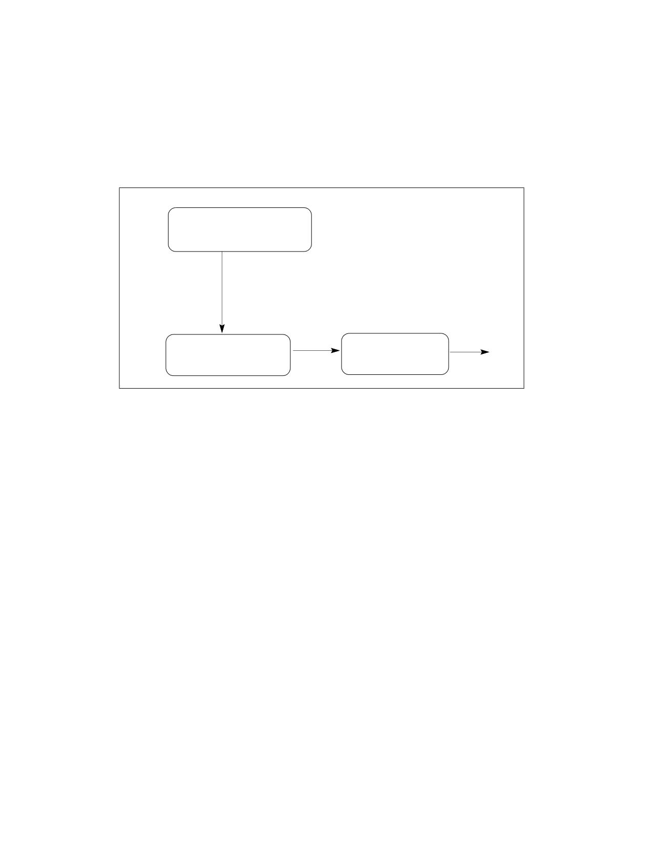
DETECTION OF INTEL® AVX INSTRUCTIONS
Intel AVX instructions operate on the 256-bit YMM register state. Application detection of new instruction exten-
sions operating on the YMM state follows the general procedural flow in Figure 14-2.
Prior to using Intel AVX, the application must identify that the operating system supports the XGETBV instruction,
the YMM register state, in addition to processor’s support for YMM state management using XSAVE/XRSTOR and
AVX instructions. The following simplified sequence accomplishes both and is strongly recommended.
1) Detect CPUID.01H:ECX.OSXSAVE[27] = 1 (XGETBV enabled for application use1).
2) Issue XGETBV and verify that XCR0[2:1] = ‘11b’ (XMM state and YMM state are enabled by OS).
3) detect CPUID.01H:ECX.AVX[28] = 1 (AVX instructions supported).
(Step 3 can be done in any order relative to 1 and 2.)
Check feature flag
CPUID.1H:ECX.OSXSAVE = 1?
OS provides processor
Yes
extended state management
Implied HW support for
XSAVE, XRSTOR, XGETBV, XCR0
Check enabled state in
Check feature flag
State
for Instruction set
ok to use
XCR0 via XGETBV
enabled
Instructions
Figure 14-2. General Procedural Flow of Application Detection of Intel® AVX
1. If CPUID.01H:ECX.OSXSAVE reports 1, it also indirectly implies the processor supports XSAVE, XRSTOR, XGETBV, processor
extended state bit vector XCR0. Thus an application may streamline the checking of CPUID feature flags for XSAVE and OSXSAVE.
XSETBV is a privileged instruction.
Vol. 1
14-15

PROGRAMMING WITH INTEL® AVX, FMA, AND INTEL® AVX2
The following pseudocode illustrates this recommended application Intel AVX detection process:
Example 14-1. Detection of Intel® AVX Instruction
INT supports_AVX()
{
mov
eax, 1
cpuid
and
ecx, 018000000H
cmp
ecx, 018000000H; check both OSXSAVE and AVX feature flags
jne
not_supported
; processor supports AVX instructions and XGETBV is enabled by OS
mov
ecx, 0; specify 0 for XCR0 register
XGETBV
; result in EDX:EAX
and
eax, 06H
cmp
eax, 06H; check OS has enabled both XMM and YMM state support
jne
not_supported
mov
eax, 1
jmp
done
NOT_SUPPORTED:
mov
eax, 0
done:
}
NOTE
It is unwise for an application to rely exclusively on CPUID.01H:ECX.AVX[28] or at all on
CPUID.01H:ECX.XSAVE[26]: These indicate hardware support but not operating system support. If
YMM state management is not enabled by an operating systems, Intel AVX instructions will #UD
regardless of CPUID.01H:ECX.AVX[28]. “CPUID.01H:ECX.XSAVE[26] = 1” does not guarantee the
OS actually uses the XSAVE process for state management.
These steps above also apply to enhanced 128-bit SIMD floating-pointing instructions in Intel AVX (using VEX
prefix-encoding) that operate on the YMM states.
14-16
Vol. 1

PROGRAMMING WITH INTEL® AVX, FMA, AND INTEL® AVX2
14.3.1 Detection of VEX-Encoded AES and VPCLMULQDQ
The VAESDEC/VAESDECLAST/VAESENC/VAESENCLAST/VAESIMC/VAESKEYGENASSIST instructions operate on
YMM states. The detection sequence must combine checking for CPUID.01H:ECX.AES[25] = 1 and the sequence
for detection application support for Intel AVX.
Example 14-2. Detection of VEX-Encoded Intel® AES-NI Instructions
INT supports_VAESNI()
{
mov
eax, 1
cpuid
and
ecx, 01A000000H
cmp
ecx, 01A000000H; check OSXSAVE AVX and AESNI feature flags
jne
not_supported
; processor supports AVX and VEX-encoded AESNI and XGETBV is enabled by OS
mov
ecx, 0; specify 0 for XCR0 register
XGETBV
; result in EDX:EAX
and
eax, 06H
cmp
eax, 06H; check OS has enabled both XMM and YMM state support
jne
not_supported
mov
eax, 1
jmp
done
NOT_SUPPORTED:
mov
eax, 0
done:
Similarly, the detection sequence for VPCLMULQDQ must combine checking for CPUID.01H:ECX.PCLMULQDQ[1] =
1 and the sequence for detection application support for Intel AVX.
This is shown in the pseudocode provided in Example 14-3.
Example 14-3. Detection of VEX-Encoded Intel® AES-NI Instructions
INT supports_VPCLMULQDQ)
{
mov
eax, 1
cpuid
and
ecx, 018000002H
cmp
ecx, 018000002H; check OSXSAVE AVX and PCLMULQDQ feature flags
jne
not_supported
; processor supports AVX and VEX-encoded PCLMULQDQ and XGETBV is enabled by OS
mov
ecx, 0; specify 0 for XCR0 register
XGETBV
; result in EDX:EAX
and
eax, 06H
cmp
eax, 06H; check OS has enabled both XMM and YMM state support
jne
not_supported
mov
eax, 1
jmp
done
NOT_SUPPORTED:
mov
eax, 0
done:
Vol. 1
14-17

PROGRAMMING WITH INTEL® AVX, FMA, AND INTEL® AVX2
14.4
HALF PRECISION FLOATING-POINT CONVERSION
VCVTPH2PS and VCVTPS2PH are two instructions supporting half precision floating-point data type conversion to
and from single precision floating-point data types.
Half precision floating-point values are not used by the processor directly for arithmetic operations. But the conver-
sion operation are subject to SIMD floating-point exceptions.
Additionally, the conversion operations of VCVTPS2PH allow programmer to specify rounding control using control
fields in an immediate byte. The effects of the immediate byte are listed in Table 14-8.
Rounding control can use Imm[2] to select an override RC field specified in Imm[1:0] or use MXCSR setting.
Table 14-8. Immediate Byte Encoding for 16-Bit Floating-Point Conversion Instructions
Bits
Field Name/value
Description
Comment
Imm[1:0]
RC=00B
Round to nearest even
If Imm[2] = 0
RC=01B
Round down
RC=10B
Round up
RC=11B
Truncate
Imm[2]
MS1=0
Use imm[1:0] for rounding
Ignore MXCSR.RC
MS1=1
Use MXCSR.RC for rounding
Imm[7:3]
Ignored
Ignored by processor
Specific SIMD floating-point exceptions that can occur in conversion operations are shown in Table 14-9 and
Table 14-10.
Table 14-9. Non-Numerical Behavior for VCVTPH2PS and VCVTPS2PH
Source Operands
Masked Result
Unmasked Result
QNaN
QNaN11
QNaN11 (not an exception)
SNaN
QNaN12
None
NOTES:
1. The half precision output QNaN1 is created from the single precision input QNaN as follows: the sign bit is preserved, the 8-bit expo-
nent FFH is replaced by the 5-bit exponent 1FH, and the 24-bit significand is truncated to an 11-bit significand by removing its 14
least significant bits.
2. The half precision output QNaN1 is created from the single precision input SNaN as follows: the sign bit is preserved, the 8-bit expo-
nent FFH is replaced by the 5-bit exponent 1FH, and the 24-bit significand is truncated to an 11-bit significand by removing its 14
least significant bits. The second most significant bit of the significand is changed from 0 to 1 to convert the signaling NaN into a quiet
NaN.
Table 14-10. Invalid Operation for VCVTPH2PS and VCVTPS2PH
Instruction
Condition
Masked Result
Unmasked Result
VCVTPH2PS
SRC = NaN
See Table 14-9
#I=1
VCVTPS2PH
SRC = NaN
See Table 14-9
#I=1
The VCVTPS2PH instruction can cause denormal exceptions if the value of the source operand is denormal relative
to the numerical range represented by the source format (see Table 14-11).
14-18
Vol. 1

PROGRAMMING WITH INTEL® AVX, FMA, AND INTEL® AVX2
Table 14-11. Denormal Condition Summary
Instruction
Condition
Masked Result
Unmasked Result
VCVTPH2PS
SRC is denormal relative to
res = Result rounded to the destination precision and
Same as masked result.
input format
using the bounded exponent, but only if no unmasked
post-computation exception occurs.
#DE unchanged
VCVTPS2PH
SRC is denormal relative to
res = Result rounded to the destination precision and
#DE=1
input format
using the bounded exponent, but only if no unmasked
post-computation exception occurs.
#DE=1
The VCVTPS2PH instruction can cause an underflow exception if the result of the conversion is less than the un-
derflow threshold for half precision floating-point data type, i.e., | x | < 1.0 ∗ 2-14.
Table 14-12. Underflow Condition for VCVTPS2PH
Instruction
Condition
Masked Result1
Unmasked Result
VCVTPS2PH
Result < smallest destination
Result = +0 or -0, denormal, normal.
#UE=1,
precision final normal value2
#UE =1.
#PE = 1 if the result is
#PE = 1 if the result is inexact.
inexact.
NOTES:
1. Masked and unmasked results are shown in Table 14-11.
2. MXCSR.FTZ is ignored, the processor behaves as if MXCSR.FTZ = 0.
The VCVTPS2PH instruction can cause an overflow exception if the result of the conversion is greater than the
maximum representable value for half precision floating-point data type, i.e., | x | ≥ 1.0 ∗ 216.
Table 14-13. Overflow Condition for VCVTPS2PH
Instruction
Condition
Masked Result
Unmasked Result
VCVTPS2PH
Result ≥ largest destination
Result = +Inf or -Inf.
#OE=1.
precision finial normal value1
#OE=1.
The VCVTPS2PH instruction can cause an inexact exception if the result of the conversion is not exactly repre-
sentable in the destination format.
Table 14-14. Inexact Condition for VCVTPS2PH
Instruction
Condition
Masked Result1
Unmasked Result
VCVTPS2PH
The result is not
res = Result rounded to the destination
Only if no underflow/overflow condition occurred,
representable in
precision and using the bounded
or if the corresponding exceptions are masked:
the destination
exponent, but only if no unmasked
• Set #OE if masked overflow and set result as
format
underflow or overflow conditions occur
described above for masked overflow.
(this exception can occur in the presence
• Set #UE if masked underflow and set result as
of a masked underflow or overflow).
described above for masked underflow.
#PE=1.
If neither underflow nor overflow, result equals
the result rounded to the destination precision and
using the bounded exponent set #PE = 1.
NOTES:
1. If a source is denormal relative to input format with DM masked and at least one of PM or UM unmasked, then an exception will be
raised with DE, UE, and PE set.
Vol. 1
14-19
PROGRAMMING WITH INTEL® AVX, FMA, AND INTEL® AVX2
14.4.1 Detection of F16C Instructions
Applications using float 16 instruction must follow a detection sequence similar to Intel AVX to ensure:
• The OS has enabled YMM state management support.
• The processor supports Intel AVX as indicated by the CPUID feature flag, i.e., CPUID.01H:ECX.AVX[28] = 1.
• The processor supports 16-bit floating-point conversion instructions via a CPUID feature flag
(CPUID.01H:ECX.F16C[29] = 1).
Application detection of Float-16 conversion instructions follow the general procedural flow in Figure 14-3.
Check feature flag
CPUID.01H:ECX.OSXSAVE = 1?
OS provides processor
extended state management
Yes
Implied HW support for
XSAVE, XRSTOR, XGETBV, XCR0
Check enabled YMM state in
Check feature flags
XCR0 via XGETBV
State
for AVX and F16C
ok to use
enabled
Instructions
Figure 14-3. General Procedural Flow of Application Detection of Float-16
----------------------------------------------------------------------------------------
INT supports_f16c()
{
; result in eax
mov eax, 1
cpuid
and ecx, 038000000H
cmp ecx, 038000000H; check OSXSAVE, AVX, F16C feature flags
jne not_supported
; processor supports AVX,F16C instructions and XGETBV is enabled by OS
mov ecx, 0; specify 0 for XCR0 register
XGETBV; result in EDX:EAX
and eax, 06H
cmp eax, 06H; check OS has enabled both XMM and YMM state support
jne not_supported
mov eax, 1
jmp done
NOT_SUPPORTED:
mov eax, 0
done:
}
-------------------------------------------------------------------------------
14-20
Vol. 1

PROGRAMMING WITH INTEL® AVX, FMA, AND INTEL® AVX2
14.5
FUSED-MULTIPLY-ADD (FMA) EXTENSIONS
FMA extensions enhances Intel AVX with high-throughput, arithmetic capabilities covering fused multiply-add,
fused multiply-subtract, fused multiply add/subtract interleave, signed-reversed multiply on fused multiply-add
and multiply-subtract. FMA extensions provide 36 256-bit floating-point instructions to perform computation on
256-bit vectors and additional 128-bit and scalar FMA instructions.
FMA extensions also provide 60 128-bit floating-point instructions to process 128-bit vector and scalar data. The
arithmetic operations cover fused multiply-add, fused multiply-subtract, signed-reversed multiply on fused
multiply-add and multiply-subtract.
Table 14-15. FMA Instructions
Instruction
Description
VFMADD132PD/VFMADD213PD/VFMADD231PD
Fused Multiply-Add of Packed Double Precision Floating-Point
xmm0, xmm1, xmm2/m128; ymm0, ymm1, ymm2/m256
Values
VFMADD132PS/VFMADD213PS/VFMADD231PS
Fused Multiply-Add of Packed Single Precision Floating-Point
xmm0, xmm1, xmm2/m128; ymm0, ymm1, ymm2/m256
Values
VFMADD132SD/VFMADD213SD/VFMADD231SD
Fused Multiply-Add of Scalar Double Precision Floating-Point
xmm0, xmm1, xmm2/m64
Values
VFMADD132SS/VFMADD213SS/VFMADD231SS
Fused Multiply-Add of Scalar Single Precision Floating-Point
xmm0, xmm1, xmm2/m32
Values
VFMADDSUB132PD/VFMADDSUB213PD/VFMADDSUB231PD
Fused Multiply-Alternating Add/Subtract of Packed Double Pre-
xmm0, xmm1, xmm2/m128; ymm0, ymm1, ymm2/m256
cision Floating-Point Values
VFMADDSUB132PS/VFMADDSUB213PS/VFMADDSUB231PS
Fused Multiply-Alternating Add/Subtract of Packed Single Pre-
xmm0, xmm1, xmm2/m128; ymm0, ymm1, ymm2/m256
cision Floating-Point Values
VFMSUBADD132PD/VFMSUBADD213PD/VFMSUBADD231PD
Fused Multiply-Alternating Subtract/Add of Packed Double Pre-
xmm0, xmm1, xmm2/m128; ymm0, ymm1, ymm2/m256
cision Floating-Point Values
VFMSUBADD132PS/VFMSUBADD213PS/VFMSUBADD231PS
Fused Multiply-Alternating Subtract/Add of Packed Single Pre-
xmm0, xmm1, xmm2/m128; ymm0, ymm1, ymm2/m256
cision Floating-Point Values
VFMSUB132PD/VFMSUB213PD/VFMSUB231PD
Fused Multiply-Subtract of Packed Double Precision Floating-
xmm0, xmm1, xmm2/m128; ymm0, ymm1, ymm2/m256
Point Values
VFMSUB132PS/VFMSUB213PS/VFMSUB231PS
Fused Multiply-Subtract of Packed Single Precision Floating-
xmm0, xmm1, xmm2/m128; ymm0, ymm1, ymm2/m256
Point Values
VFMSUB132SD/VFMSUB213SD/VFMSUB231SD
Fused Multiply-Subtract of Scalar Double Precision Floating-
xmm0, xmm1, xmm2/m64
Point Values
VFMSUB132SS/VFMSUB213SS/VFMSUB231SS
Fused Multiply-Subtract of Scalar Single Precision Floating-
xmm0, xmm1, xmm2/m32
Point Values
VFNMADD132PD/VFNMADD213PD/VFNMADD231PD
Fused Negative Multiply-Add of Packed Double Precision Float-
xmm0, xmm1, xmm2/m128; ymm0, ymm1, ymm2/m256
ing-Point Values
VFNMADD132PS/VFNMADD213PS/VFNMADD231PS
Fused Negative Multiply-Add of Packed Single Precision Float-
xmm0, xmm1, xmm2/m128; ymm0, ymm1, ymm2/m256
ing-Point Values
VFNMADD132SD/VFNMADD213SD/VFNMADD231SD
Fused Negative Multiply-Add of Scalar Double Precision Float-
xmm0, xmm1, xmm2/m64
ing-Point Values
VFNMADD132SS/VFNMADD213SS/VFNMADD231SS
Fused Negative Multiply-Add of Scalar Single Precision Float-
xmm0, xmm1, xmm2/m32
ing-Point Values
VFNMSUB132PD/VFNMSUB213PD/VFNMSUB231PD
Fused Negative Multiply-Subtract of Packed Double Precision
xmm0, xmm1, xmm2/m128; ymm0, ymm1, ymm2/m256
Floating-Point Values
VFNMSUB132PS/VFNMSUB213PS/VFNMSUB231PS
Fused Negative Multiply-Subtract of Packed Single Precision
xmm0, xmm1, xmm2/m128; ymm0, ymm1, ymm2/m256
Floating-Point Values
Vol. 1
14-21

PROGRAMMING WITH INTEL® AVX, FMA, AND INTEL® AVX2
Table 14-15. FMA Instructions (Contd.)
Instruction
Description
VFNMSUB132SD/VFNMSUB213SD/VFNMSUB231SD
Fused Negative Multiply-Subtract of Scalar Double Precision
xmm0, xmm1, xmm2/m64
Floating-Point Values
VFNMSUB132SS/VFNMSUB213SS/VFNMSUB231SS
Fused Negative Multiply-Subtract of Scalar Single Precision
xmm0, xmm1, xmm2/m32
Floating-Point Values
14.5.1 FMA Instruction Operand Order and Arithmetic Behavior
FMA instruction mnemonics are defined explicitly with an ordered three digits, e.g., VFMADD132PD. The value of
each digit refers to the ordering of the three source operand as defined by instruction encoding specification:
•
‘1’: The first source operand (also the destination operand) in the syntactical order listed in this specification.
•
‘2’: The second source operand in the syntactical order. This is a YMM/XMM register, encoded using VEX prefix.
•
‘3’: The third source operand in the syntactical order. The first and third operand are encoded following ModR/M
encoding rules.
The ordering of each digit within the mnemonic refers to the floating-point data listed on the right-hand side of the
arithmetic equation of each FMA operation (see Table 14-17):
• The first position in the three digits of a FMA mnemonic refers to the operand position of the first FP data
expressed in the arithmetic equation of FMA operation, the multiplicand.
• The second position in the three digits of a FMA mnemonic refers to the operand position of the second FP data
expressed in the arithmetic equation of FMA operation, the multiplier.
• The third position in the three digits of a FMA mnemonic refers to the operand position of the FP data being
added/subtracted to the multiplication result.
Note the non-numerical result of an FMA operation does not resemble the mathematically-defined commutative
property between the multiplicand and the multiplier values (see Table 14-17). Consequently, software tools (such
as an assembler) may support a complementary set of FMA mnemonics for each FMA instruction for ease of
programming to take advantage of the mathematical property of commutative multiplications. For example, an
assembler may optionally support the complementary mnemonic “VFMADD312PD” in addition to the true
mnemonic “VFMADD132PD“. The assembler will generate the same instruction opcode sequence corresponding to
VFMADD132PD. The processor executes VFMADD132PD and report any NAN conditions based on the definition of
VFMADD132PD. Similarly, if the complementary mnemonic VFMADD123PD is supported by an assembler at source
level, it must generate the opcode sequence corresponding to VFMADD213PD; the complementary mnemonic
VFMADD321PD must produce the opcode sequence defined by VFMADD231PD. In the absence of FMA operations
reporting a NAN result, the numerical results of using either mnemonic with an assembler supporting both
mnemonics will match the behavior defined in Table 14-17. Support for the complementary FMA mnemonics by
software tools is optional.
14.5.2 Fused-Multiply-ADD (FMA) Numeric Behavior
FMA instructions can perform fused-multiply-add operations (including fused-multiply-subtract, and other vari-
eties) on packed and scalar data elements in the instruction operands. Separate FMA instructions are provided to
handle different types of arithmetic operations on the three source operands.
FMA instruction syntax is defined using three source operands and the first source operand is updated based on the
result of the arithmetic operations of the data elements of 128-bit or 256-bit operands, i.e., The first source
operand is also the destination operand.
The arithmetic FMA operation performed in an FMA instruction takes one of several forms, r=(x*y)+z, r=(x*y)-z,
r=-(x*y)+z, or r=-(x*y)-z. Packed FMA instructions can perform eight single precision FMA operations or four
double precision FMA operations with 256-bit vectors.
Scalar FMA instructions only perform one arithmetic operation on the low order data element. The content of the
rest of the data elements in the lower 128-bits of the destination operand is preserved. the upper 128bits of the
destination operand are filled with zero.
14-22
Vol. 1

PROGRAMMING WITH INTEL® AVX, FMA, AND INTEL® AVX2
An arithmetic FMA operation of the form, r=(x*y)+z, takes two IEEE-754-2008 single (double) precision values
and multiplies them to form an infinite precision intermediate value. This intermediate value is added to a third
single (double) precision value (also at infinite precision) and rounded to produce a single (double) precision result.
Table 14-17 describes the numerical behavior of the FMA operation, r=(x*y)+z, r=(x*y)-z, r=-(x*y)+z, r=-(x*y)-
z for various input values. The input values can be 0, finite non-zero (F in Table 14-17), infinity of either sign (INF
in Table 14-17), positive infinity (+INF in Table 14-17), negative infinity (-INF in Table 14-17), or NaN (including
QNaN or SNaN). If any one of the input values is a NAN, the result of FMA operation, r, may be a quietized NAN. The
result can be either Q(x), Q(y), or Q(z), see Table 14-17. If x is a NaN, then:
• Q(x) = x if x is QNaN, or
• Q(x) = the quietized NaN obtained from x if x is SNaN.
The notation for the output value in Table 14-17 are:
•
“+INF”: positive infinity, “-INF”: negative infinity. When the result depends on a conditional expression, both
values are listed in the result column and the condition is described in the comment column.
• QNaNIndefinite represents the QNaN which has the sign bit equal to 1, the most significand field equal to 1, and
the remaining significand field bits equal to 0.
• The summation or subtraction of 0s or identical values in FMA operation can lead to the following situations
shown in Table 14-16.
• If the FMA computation represents an invalid operation (e.g., when adding two INF with opposite signs)), the
invalid exception is signaled, and the MXCSR.IE flag is set.
Table 14-16. Rounding Behavior of Zero Result in FMA Operation
x*y
z
(x*y) + z
(x*y) - z
- (x*y) + z
- (x*y) - z
+0 in all rounding modes
- 0 when rounding down,
- 0 when rounding down,
- 0 in all rounding modes
(+0)
(+0)
and +0 otherwise
and +0 otherwise
- 0 when rounding down,
+0 in all rounding modes
- 0 in all rounding modes
- 0 when rounding down,
(+0)
(-0)
and +0 otherwise
and +0 otherwise
- 0 when rounding down,
- 0 in all rounding modes
+ 0 in all rounding modes
- 0 when rounding down,
(-0)
(+0)
and +0 otherwise
and +0 otherwise
- 0 in all rounding modes
- 0 when rounding down,
- 0 when rounding down,
+ 0 in all rounding modes
(-0)
(-0)
and +0 otherwise
and +0 otherwise
- 0 when rounding down,
2*F
-2*F
- 0 when rounding down,
F
-F
and +0 otherwise
and +0 otherwise
2*F
- 0 when rounding down,
- 0 when rounding down,
-2*F
F
F
and +0 otherwise
and +0 otherwise
Table 14-17. FMA Numeric Behavior
x
y
r=(x*y)
r=(x*y)
r =
r=
z
Comment
(multiplicand)
(multiplier)
+z
-z
-(x*y)+z
-(x*y)-z
NaN
0, F, INF,
0, F,
Q(x)
Q(x)
Q(x)
Q(x)
Signal invalid exception if x or y or z is SNaN
NaN
INF,
NaN
0, F, INF
NaN
0, F,
Q(y)
Q(y)
Q(y)
Q(y)
Signal invalid exception if y or z is SNaN
INF,
NaN
0, F, INF
0, F, INF
NaN
Q(z)
Q(z)
Q(z)
Q(z)
Signal invalid exception if z is SNaN
INF
F, INF
+IN
+INF
QNaNIn-
QNaNIn-
-INF
if x*y and z have the same sign
F
definite
definite
QNaNIn-
-INF
+INF
QNaNIn-
if x*y and z have opposite signs
definite
definite
Vol. 1
14-23

PROGRAMMING WITH INTEL® AVX, FMA, AND INTEL® AVX2
x
y
r=(x*y)
r=(x*y)
r =
r=
z
Comment
(multiplicand)
(multiplier)
+z
-z
-(x*y)+z
-(x*y)-z
INF
F, INF
-INF
-INF
QNaNIn-
QNaNIn-
+INF
if x*y and z have the same sign
definite
definite
QNaNIn-
+INF
-INF
QNaNIn-
if x*y and z have opposite signs
definite
definite
INF
F, INF
0, F
+INF
+INF
-INF
-INF
if x and y have the same sign
-INF
-INF
+INF
+INF
if x and y have opposite signs
INF
0
0, F,
QNaNIn-
QNaNIn-
QNaNIn-
QNaNIn-
Signal invalid exception
INF
definite
definite
definite
definite
0
INF
0, F,
QNaNIn-
QNaNIn-
QNaNIn-
QNaNIn-
Signal invalid exception
INF
definite
definite
definite
definite
F
INF
+IN
+INF
QNaNIn-
QNaNIn-
-INF
if x*y and z have the same sign
F
definite
definite
QNaNIn-
-INF
+INF
QNaNIn-
if x*y and z have opposite signs
definite
definite
F
INF
-INF
-INF
QNaNIn-
QNaNIn-
+INF
if x*y and z have the same sign
definite
definite
QNaNIn-
+INF
-INF
QNaNIn-
if x*y and z have opposite signs
definite
definite
F
INF
0,F
+INF
+INF
-INF
-INF
if x * y > 0
-INF
-INF
+INF
+INF
if x * y < 0
0,F
0,F
INF
+INF
-INF
+INF
-INF
if z > 0
-INF
+INF
-INF
+INF
if z < 0
0
0
0
0
0
0
0
The sign of the result depends on the sign of
the operands and on the rounding mode. The
0
F
0
0
0
0
0
product x*y is +0 or -0, depending on the signs
F
0
0
0
0
0
0
of x and y. The summation/subtraction of the
zero representing (x*y) and the zero represent-
ing z can lead to one of the four cases shown in
Table 14-16.
0
0
F
z
-z
z
-z
0
F
F
z
-z
z
-z
F
0
F
z
-z
z
-z
F
F
0
x*y
x*y
-x*y
-x*y
Rounded to the destination precision, with
bounded exponent
F
F
F
(x*y)+z
(x*y)-z
-(x*y)+z
-(x*y)-z
Rounded to the destination precision, with
bounded exponent; however, if the exact values
of x*y and z are equal in magnitude with signs
resulting in the FMA operation producing 0, the
rounding behavior described in Table 14-16.
If unmasked floating-point exceptions are signaled (invalid operation, denormal operand, overflow, underflow, or
inexact result) the result register is left unchanged and a floating-point exception handler is invoked.
14.5.3 Detection of FMA
Hardware support for FMA is indicated by CPUID.01H:ECX.FMA[12]=1.
Application Software must identify that hardware supports AVX, after that it must also detect support for FMA by
CPUID.01H:ECX.FMA[12]. The recommended pseudocode sequence for detection of FMA is:
----------------------------------------------------------------------------------------
14-24
Vol. 1
PROGRAMMING WITH INTEL® AVX, FMA, AND INTEL® AVX2
INT supports_fma()
{
; result in eax
mov eax, 1
cpuid
and ecx, 018001000H
cmp ecx, 018001000H; check OSXSAVE, AVX, FMA feature flags
jne not_supported
; processor supports AVX,FMA instructions and XGETBV is enabled by OS
mov ecx, 0; specify 0 for XCR0 register
XGETBV; result in EDX:EAX
and eax, 06H
cmp eax, 06H; check OS has enabled both XMM and YMM state support
jne not_supported
mov eax, 1
jmp done
NOT_SUPPORTED:
mov eax, 0
done:
}
-------------------------------------------------------------------------------
Note that FMA comprises 256-bit and 128-bit SIMD instructions operating on YMM states.
14.6
OVERVIEW OF INTEL® ADVANCED VECTOR EXTENSIONS 2 (INTEL® AVX2)
Intel® AVX2 extends Intel AVX by promoting most of the 128-bit SIMD integer instructions with 256-bit numeric
processing capabilities. Intel AVX2 instructions follow the same programming model as AVX instructions.
In addition, Intel AVX2 provide enhanced functionalities for broadcast/permute operations on data elements,
vector shift instructions with variable-shift count per data element, and instructions to fetch non-contiguous data
elements from memory.
14.6.1 Intel® AVX2 and 256-Bit Vector Integer Processing
Intel AVX2 promotes the vast majority of 128-bit integer SIMD instruction sets to operate with 256-bit wide YMM
registers. Intel AVX2 instructions are encoded using the VEX prefix and require the same operating system support
as Intel AVX. Generally, most of the promoted 256-bit vector integer instructions follow the 128-bit lane operation,
similar to the promoted 256-bit floating-point SIMD instructions in Intel AVX.
Newer functionalities in Intel AVX2 generally fall into the following categories:
• Fetching non-contiguous data elements from memory using vector-index memory addressing. These “gather”
instructions introduce a new memory-addressing form, consisting of a base register and multiple indices
specified by a vector register (either XMM or YMM). Data elements sizes of 32 and 64-bits are supported, and
data types for floating-point and integer elements are also supported.
• Cross-lane functionalities are provided with several new instructions for broadcast and permute operations.
Some of the 256-bit vector integer instructions promoted from legacy SSE instruction sets also exhibit cross-
lane behavior, e.g., VPMOVZ/VPMOVS family.
• Intel AVX2 complements the Intel AVX instructions that are typed for floating-point operation with a full
complement of equivalent set for operating with 32/64-bit integer data elements.
• Vector shift instructions with per-element shift count. Data elements sizes of 32 and 64 bits are supported.
Vol. 1
14-25

PROGRAMMING WITH INTEL® AVX, FMA, AND INTEL® AVX2
14.7
PROMOTED VECTOR INTEGER INSTRUCTIONS IN INTEL® AVX2
In Intel AVX2, most SSSE3 and Intel SSE, SSE2, SSE3, and SSE4 vector integer instructions have been promoted
to support VEX.256 encodings. Table 14-18 summarizes the promotion status for existing instructions. The column
“VEX.128” indicates whether the instruction using VEX.128 prefix encoding is supported.
The column “VEX.256” indicates whether 256-bit vector form of the instruction using the VEX.256 prefix encoding
is supported, and under which feature flag.
Table 14-18. Promoted Vector Integer SIMD Instructions in Intel® AVX2
VEX.256 Encoding
VEX.128 Encoding
Group
Instruction
AVX2
AVX
YY 0F 6X
PUNPCKLBW
AVX2
AVX
PUNPCKLWD
AVX2
AVX
PUNPCKLDQ
AVX2
AVX
PACKSSWB
AVX2
AVX
PCMPGTB
AVX2
AVX
PCMPGTW
AVX2
AVX
PCMPGTD
AVX2
AVX
PACKUSWB
AVX2
AVX
PUNPCKHBW
AVX2
AVX
PUNPCKHWD
AVX2
AVX
PUNPCKHDQ
AVX2
AVX
PACKSSDW
AVX2
AVX
PUNPCKLQDQ
AVX2
AVX
PUNPCKHQDQ
no
AVX
MOVD
no
AVX
MOVQ
AVX
AVX
MOVDQA
AVX
AVX
MOVDQU
AVX2
AVX
YY 0F 7X
PSHUFD
AVX2
AVX
PSHUFHW
AVX2
AVX
PSHUFLW
AVX2
AVX
PCMPEQB
AVX2
AVX
PCMPEQW
AVX2
AVX
PCMPEQD
AVX
AVX
MOVDQA
AVX
AVX
MOVDQU
no
AVX
PINSRW
no
AVX
PEXTRW
AVX2
AVX
PSRLW
AVX2
AVX
PSRLD
AVX2
AVX
PSRLQ
AVX2
AVX
PADDQ
AVX2
AVX
PMULLW
14-26
Vol. 1

PROGRAMMING WITH INTEL® AVX, FMA, AND INTEL® AVX2
Table 14-18. Promoted Vector Integer SIMD Instructions in Intel® AVX2 (Contd.)
VEX.256 Encoding
VEX.128 Encoding
Group
Instruction
AVX2
AVX
PMOVMSKB
AVX2
AVX
PSUBUSB
AVX2
AVX
PSUBUSW
AVX2
AVX
PMINUB
AVX2
AVX
PAND
AVX2
AVX
PADDUSB
AVX2
AVX
PADDUSW
AVX2
AVX
PMAXUB
AVX2
AVX
PANDN
AVX2
AVX
YY 0F EX
PAVGB
AVX2
AVX
PSRAW
AVX2
AVX
PSRAD
AVX2
AVX
PAVGW
AVX2
AVX
PMULHUW
AVX2
AVX
PMULHW
AVX
AVX
MOVNTDQ
AVX2
AVX
PSUBSB
AVX2
AVX
PSUBSW
AVX2
AVX
PMINSW
AVX2
AVX
POR
AVX2
AVX
PADDSB
AVX2
AVX
PADDSW
AVX2
AVX
PMAXSW
AVX2
AVX
PXOR
AVX
AVX
YY 0F FX
LDDQU
AVX2
AVX
PSLLW
AVX2
AVX
PSLLD
AVX2
AVX
PSLLQ
AVX2
AVX
PMULUDQ
AVX2
AVX
PMADDWD
AVX2
AVX
PSADBW
AVX2
AVX
PSUBB
AVX2
AVX
PSUBW
AVX2
AVX
PSUBD
AVX2
AVX
PSUBQ
AVX2
AVX
PADDB
AVX2
AVX
PADDW
AVX2
AVX
PADDD
Vol. 1
14-27

PROGRAMMING WITH INTEL® AVX, FMA, AND INTEL® AVX2
Table 14-18. Promoted Vector Integer SIMD Instructions in Intel® AVX2 (Contd.)
VEX.256 Encoding
VEX.128 Encoding
Group
Instruction
AVX2
AVX
SSSE3
PHADDW
AVX2
AVX
PHADDSW
AVX2
AVX
PHADDD
AVX2
AVX
PHSUBW
AVX2
AVX
PHSUBSW
AVX2
AVX
PHSUBD
AVX2
AVX
PMADDUBSW
AVX2
AVX
PALIGNR
AVX2
AVX
PSHUFB
AVX2
AVX
PMULHRSW
AVX2
AVX
PSIGNB
AVX2
AVX
PSIGNW
AVX2
AVX
PSIGND
AVX2
AVX
PABSB
AVX2
AVX
PABSW
AVX2
AVX
PABSD
AVX2
AVX
MOVNTDQA
AVX2
AVX
MPSADBW
AVX2
AVX
PACKUSDW
AVX2
AVX
PBLENDVB
AVX2
AVX
PBLENDW
AVX2
AVX
PCMPEQQ
no
AVX
PEXTRD
no
AVX
PEXTRQ
no
AVX
PEXTRB
no
AVX
PEXTRW
no
AVX
PHMINPOSUW
no
AVX
PINSRB
no
AVX
PINSRD
no
AVX
PINSRQ
AVX2
AVX
PMAXSB
AVX2
AVX
PMAXSD
AVX2
AVX
PMAXUD
AVX2
AVX
PMAXUW
AVX2
AVX
PMINSB
AVX2
AVX
PMINSD
AVX2
AVX
PMINUD
AVX2
AVX
PMINUW
14-28
Vol. 1

PROGRAMMING WITH INTEL® AVX, FMA, AND INTEL® AVX2
Table 14-18. Promoted Vector Integer SIMD Instructions in Intel® AVX2 (Contd.)
VEX.256 Encoding
VEX.128 Encoding
Group
Instruction
AVX2
AVX
PMOVSXxx
AVX2
AVX
PMOVZXxx
AVX2
AVX
PMULDQ
AVX2
AVX
PMULLD
AVX
AVX
PTEST
AVX2
AVX
SSE4.2
PCMPGTQ
no
AVX
PCMPESTRI
no
AVX
PCMPESTRM
no
AVX
PCMPISTRI
no
AVX
PCMPISTRM
no
AVX
AESNI
AESDEC
no
AVX
AESDECLAST
no
AVX
AESENC
no
AVX
AESECNLAST
no
AVX
AESIMC
no
AVX
AESKEYGENASSIST
no
AVX
CLMUL
PCLMULQDQ
Table 14-19 compares complementary SIMD functionalities introduced in Intel AVX and AVX2. instructions.
Table 14-19. VEX-Only SIMD Instructions in Intel® AVX and AVX2
lntel® AVX2
Intel® AVX
Comment
VBROADCASTI128
VBROADCASTF128
256-bit only
VBROADCASTSD ymm1, xmm
VBROADCASTSD ymm1, m64
256-bit only
VBROADCASTSS (from xmm)
VBROADCASTSS (from m32)
VEXTRACTI128
VEXTRACTF128
256-bit only
VINSERTI128
VINSERTF128
256-bit only
VPMASKMOVD
VMASKMOVPS
VPMASKMOVQ!
VMASKMOVPD
VPERMILPD
in-lane
VPERMILPS
in-lane
VPERM2I128
VPERM2F128
256-bit only
VPERMD
cross-lane
VPERMPS
cross-lane
VPERMQ
cross-lane
VPERMPD
cross-lane
VTESTPD
VTESTPS
Vol. 1
14-29

PROGRAMMING WITH INTEL® AVX, FMA, AND INTEL® AVX2
Table 14-19. VEX-Only SIMD Instructions in Intel® AVX and AVX2 (Contd.)
lntel® AVX2
Intel® AVX
Comment
VPBLENDD
VPSLLVD/Q
VPSRAVD
VPSRLVD/Q
VGATHERDPD/QPD
VGATHERDPS/QPS
VPGATHERDD/QD
VPGATHERDQ/QQ
Table 14-20. New Primitive in Intel® AVX2 Instructions
Instruction
Description
VPERMD ymm1, ymm2, ymm3/m256
Permute doublewords in ymm3/m256 using indexes in ymm2 and store the result in ymm1.
VPERMPD ymm1, ymm2/m256, imm8
Permute double precision FP elements in ymm2/m256 using indexes in imm8 and store the
result in ymm1.
VPERMPS ymm1, ymm2, ymm3/m256
Permute single precision FP elements in ymm3/m256 using indexes in ymm2 and store the
result in ymm1.
VPERMQ ymm1, ymm2/m256, imm8
Permute quadwords in ymm2/m256 using indexes in imm8 and store the result in ymm1.
VPSLLVD xmm1, xmm2, xmm3/m128
Shift doublewords in xmm2 left by amount specified in the corresponding element of
xmm3/m128 while shifting in 0s.
VPSLLVQ xmm1, xmm2, xmm3/m128
Shift quadwords in xmm2 left by amount specified in the corresponding element of
xmm3/m128 while shifting in 0s.
VPSLLVD ymm1, ymm2, ymm3/m256
Shift doublewords in ymm2 left by amount specified in the corresponding element of
ymm3/m256 while shifting in 0s.
VPSLLVQ ymm1, ymm2, ymm3/m256
Shift quadwords in ymm2 left by amount specified in the corresponding element of
ymm3/m256 while shifting in 0s.
VPSRAVD xmm1, xmm2, xmm3/m128
Shift doublewords in xmm2 right by amount specified in the corresponding element of
xmm3/m128 while shifting in the sign bits.
VPSRLVD xmm1, xmm2, xmm3/m128
Shift doublewords in xmm2 right by amount specified in the corresponding element of
xmm3/m128 while shifting in 0s.
VPSRLVQ xmm1, xmm2, xmm3/m128
Shift quadwords in xmm2 right by amount specified in the corresponding element of
xmm3/m128 while shifting in 0s.
VPSRLVD ymm1, ymm2, ymm3/m256
Shift doublewords in ymm2 right by amount specified in the corresponding element of
ymm3/m256 while shifting in 0s.
VPSRLVQ ymm1, ymm2, ymm3/m256
Shift quadwords in ymm2 right by amount specified in the corresponding element of
ymm3/m256 while shifting in 0s.
VGATHERDD xmm1, vm32x, xmm2
Using dword indices specified in vm32x, gather dword values from memory conditioned on
mask specified by xmm2. Conditionally gathered elements are merged into xmm1.
VGATHERQD xmm1, vm64x, xmm2
Using qword indices specified in vm64x, gather dword values from memory conditioned on
mask specified by xmm2. Conditionally gathered elements are merged into xmm1.
VGATHERDD ymm1, vm32y, ymm2
Using dword indices specified in vm32y, gather dword values from memory conditioned on
mask specified by ymm2. Conditionally gathered elements are merged into ymm1.
VGATHERQD ymm1, vm64y, ymm2
Using qword indices specified in vm64y, gather dword values from memory conditioned on
mask specified by ymm2. Conditionally gathered elements are merged into ymm1.
14-30
Vol. 1

PROGRAMMING WITH INTEL® AVX, FMA, AND INTEL® AVX2
Instruction
Description
VGATHERDPD xmm1, vm32x, xmm2
Using dword indices specified in vm32x, gather double precision FP values from memory
conditioned on mask specified by xmm2. Conditionally gathered elements are merged into
xmm1.
VGATHERQPD xmm1, vm64x, xmm2
Using qword indices specified in vm64x, gather double precision FP values from memory
conditioned on mask specified by xmm2. Conditionally gathered elements are merged into
xmm1.
VGATHERDPD ymm1, vm32x, ymm2
Using dword indices specified in vm32x, gather double precision FP values from memory
conditioned on mask specified by ymm2. Conditionally gathered elements are merged into
ymm1.
VGATHERQPD ymm1, vm64y ymm2
Using qword indices specified in vm64y, gather double precision FP values from memory
conditioned on mask specified by ymm2. Conditionally gathered elements are merged into
ymm1.
VGATHERDPS xmm1, vm32x, xmm2
Using dword indices specified in vm32x, gather single precision FP values from memory con-
ditioned on mask specified by xmm2. Conditionally gathered elements are merged into
xmm1.
VGATHERQPS xmm1, vm64x, xmm2
Using qword indices specified in vm64x, gather single precision FP values from memory con-
ditioned on mask specified by xmm2. Conditionally gathered elements are merged into
xmm1.
VGATHERDPS ymm1, vm32y, ymm2
Using dword indices specified in vm32y, gather single precision FP values from memory con-
ditioned on mask specified by ymm2. Conditionally gathered elements are merged into
ymm1.
VGATHERQPS xmm1, vm64y, xmm2
Using qword indices specified in vm64y, gather single precision FP values from memory con-
ditioned on mask specified by xmm2. Conditionally gathered elements are merged into
xmm1.
VGATHERDQ xmm1, vm32x, xmm2
Using dword indices specified in vm32x, gather qword values from memory conditioned on
mask specified by xmm2. Conditionally gathered elements are merged into xmm1.
VGATHERQQ xmm1, vm64x, xmm2
Using qword indices specified in vm64x, gather qword values from memory conditioned on
mask specified by xmm2. Conditionally gathered elements are merged into xmm1.
VGATHERDQ ymm1, vm32x, ymm2
Using dword indices specified in vm32x, gather qword values from memory conditioned on
mask specified by ymm2. Conditionally gathered elements are merged into ymm1.
VGATHERQQ ymm1, vm64y, ymm2
Using qword indices specified in vm64y, gather qword values from memory conditioned on
mask specified by ymm2. Conditionally gathered elements are merged into ymm1.
14.7.1 Detection of Intel® AVX2
Hardware support for Intel AVX2 is indicated by CPUID.07H.00H:EBX.AVX2[5] =1.
Application Software must identify that hardware supports Intel AVX, after that it must also detect support for Intel
AVX2 by checking CPUID.07H.00H:EBX.AVX2[5]. The recommended pseudocode sequence for detection of Intel
AVX2 is:
----------------------------------------------------------------------------------------
INT supports_avx2()
{
; result in eax
mov eax, 1
cpuid
and ecx, 018000000H
cmp ecx, 018000000H; check both OSXSAVE and AVX feature flags
jne not_supported
; processor supports AVX instructions and XGETBV is enabled by OS
mov eax, 7
Vol. 1
14-31
PROGRAMMING WITH INTEL® AVX, FMA, AND INTEL® AVX2
mov ecx, 0
cpuid
and ebx, 20H
cmp ebx, 20H; check AVX2 feature flags
jne not_supported
mov ecx, 0; specify 0 for XCR0 register
XGETBV; result in EDX:EAX
and eax, 06H
cmp eax, 06H; check OS has enabled both XMM and YMM state support
jne not_supported
mov eax, 1
jmp done
NOT_SUPPORTED:
mov eax, 0
done:
}
-------------------------------------------------------------------------------
14.8
ACCESSING YMM REGISTERS
The lower 128 bits of a YMM register is aliased to the corresponding XMM register. Legacy SSE instructions (i.e.,
SIMD instructions operating on XMM state but not using the VEX prefix, also referred to non-VEX encoded SIMD
instructions) will not access the upper bits (255:128) of the YMM registers. AVX and FMA instructions with a VEX
prefix and vector length of 128-bits zeroes the upper 128 bits of the YMM register.
Upper bits of YMM registers (255:128) can be read and written by many instructions with a VEX.256 prefix.
XSAVE and XRSTOR may be used to save and restore the upper bits of the YMM registers.
14.9
MEMORY ALIGNMENT
Memory alignment requirements on VEX-encoded instruction differs from non-VEX-encoded instructions. Memory
alignment applies to non-VEX-encoded SIMD instructions in three categories:
• Explicitly-aligned SIMD load and store instructions accessing 16 bytes of memory (e.g., MOVAPD, MOVAPS,
MOVDQA, etc.). These instructions always require memory address to be aligned on 16-byte boundary.
• Explicitly-unaligned SIMD load and store instructions accessing 16 bytes or less of data from memory (e.g.,
MOVUPD, MOVUPS, MOVDQU, MOVQ, MOVD, etc.). These instructions do not require memory address to be
aligned on 16-byte boundary.
• The vast majority of arithmetic and data processing instructions in legacy SSE instructions (non-VEX-encoded
SIMD instructions) support memory access semantics. When these instructions access 16 bytes of data from
memory, the memory address must be aligned on 16-byte boundary.
Most arithmetic and data processing instructions encoded using the VEX prefix and performing memory accesses
have more flexible memory alignment requirements than instructions that are encoded without the VEX prefix.
Specifically,
• With the exception of explicitly aligned 16 or 32 byte SIMD load/store instructions, most VEX-encoded,
arithmetic and data processing instructions operate in a flexible environment regarding memory address
alignment, i.e., VEX-encoded instruction with 32-byte or 16-byte load semantics will support unaligned load
operation by default. Memory arguments for most instructions with VEX prefix operate normally without
14-32
Vol. 1

PROGRAMMING WITH INTEL® AVX, FMA, AND INTEL® AVX2
causing #GP(0) on any byte-granularity alignment (unlike Legacy SSE instructions). The instructions that
require explicit memory alignment requirements are listed in Table 14-22.
Software may see performance penalties when unaligned accesses cross cacheline boundaries, so reasonable
attempts to align commonly used data sets should continue to be pursued.
Atomic memory operation in Intel 64 and IA-32 architecture is guaranteed only for a subset of memory operand
sizes and alignment scenarios. The list of guaranteed atomic operations are described in Section 11.1.1 of the
Intel® 64 and IA-32 Architectures Software Developer’s Manual, Volume 3A. Intel AVX and FMA instructions do not
introduce any new guaranteed atomic memory operations.
Intel AVX instructions can generate an #AC(0) fault on misaligned 4 or 8-byte memory references in Ring-3 when
CR0.AM= 1. 16 and 32-byte memory references will not generate #AC(0) fault. See Table 14-21 for details.
Certain Intel AVX instructions always require 16- or 32-byte alignment (see the complete list of such instructions
in Table 14-22). These instructions will #GP(0) if not aligned to 16-byte boundaries (for 16-byte granularity loads
and stores) or 32-byte boundaries (for 32-byte loads and stores).
Table 14-21. Alignment Faulting Conditions when Memory Access is Not Aligned
EFLAGS.AC==1 && Ring-3 && CR0.AM == 1
0
1
16- or 32-byte “explicitly unaligned” loads and stores (see Table
no fault
no fault
14-23)
VEX op YMM, m256
no fault
no fault
VEX op XMM, m128
no fault
no fault
“explicitly aligned” loads and stores (see Table 14-22)
#GP(0)
#GP(0)
2, 4, or 8-byte loads and stores
no fault
#AC(0)
16 byte “explicitly unaligned” loads and stores (see Table 14-23)
no fault
no fault
op XMM, m128
#GP(0)
#GP(0)
“explicitly aligned” loads and stores (see Table 14-22)
#GP(0)
#GP(0)
2, 4, or 8-byte loads and stores
no fault
#AC(0)
Table 14-22. Instructions Requiring Explicitly Aligned Memory
Require 16-byte alignment
Require 32-byte alignment
(V)MOVDQA xmm, m128
VMOVDQA ymm, m256
(V)MOVDQA m128, xmm
VMOVDQA m256, ymm
(V)MOVAPS xmm, m128
VMOVAPS ymm, m256
(V)MOVAPS m128, xmm
VMOVAPS m256, ymm
(V)MOVAPD xmm, m128
VMOVAPD ymm, m256
(V)MOVAPD m128, xmm
VMOVAPD m256, ymm
(V)MOVNTPS m128, xmm
VMOVNTPS m256, ymm
(V)MOVNTPD m128, xmm
VMOVNTPD m256, ymm
(V)MOVNTDQ m128, xmm
VMOVNTDQ m256, ymm
(V)MOVNTDQA xmm, m128
VMOVNTDQA ymm, m256
Vol. 1
14-33

PROGRAMMING WITH INTEL® AVX, FMA, AND INTEL® AVX2
Table 14-23. Instructions Not Requiring Explicit Memory Alignment
(V)MOVDQU xmm, m128
(V)MOVDQU m128, m128
(V)MOVUPS xmm, m128
(V)MOVUPS m128, xmm
(V)MOVUPD xmm, m128
(V)MOVUPD m128, xmm
VMOVDQU ymm, m256
VMOVDQU m256, ymm
VMOVUPS ymm, m256
VMOVUPS m256, ymm
VMOVUPD ymm, m256
VMOVUPD m256, ymm
14.10 SIMD FLOATING-POINT EXCEPTIONS
Intel AVX instructions can generate SIMD floating-point exceptions (#XM) and respond to exception masks in the
same way as Legacy SSE instructions. When CR4.OSXMMEXCPT=0 any unmasked FP exceptions generate an
Undefined Opcode exception (#UD).
Intel AVX FP exceptions are created in a similar fashion (differing only in number of elements) to Legacy SSE and
SSE2 instructions capable of generating SIMD floating-point exceptions.
AVX introduces no new arithmetic operations (AVX floating-point are analogues of existing Legacy SSE instruc-
tions).
F16C, FMA instructions can generate SIMD floating-point exceptions (#XM). The requirements that apply to Intel
AVX also apply to F16C and FMA.
The subset of Intel AVX2 instructions that operate on floating-point data do not generate #XM.
The detailed exception conditions for Intel AVX instructions and legacy SIMD instructions (excluding instructions
that operates on MMX registers) are described in a number of exception class types, depending on the operand
syntax and memory operation characteristics. The complete list of SIMD instruction exception class types are
defined in Chapter 2, “Instruction Format,” of the Intel® 64 and IA-32 Architectures Software Developer’s Manual,
Volume 2A.
14.11 EMULATION
Setting the CR0.EMbit to 1 provides a technique to emulate Legacy SSE floating-point instruction sets in software.
This technique is not supported with AVX instructions.
If an operating system wishes to emulate AVX instructions, set XCR0[2:1] to zero. This will cause AVX instructions
to #UD. Emulation of F16C, AVX2, and FMA by operating system can be done similarly as with emulating AVX
instructions.
14.12 WRITING INTEL® AVX FLOATING-POINT EXCEPTION HANDLERS
Intel AVX and FMA floating-point exceptions are handled in an entirely analogous way to Legacy SSE floating-point
exceptions. To handle unmasked SIMD floating-point exceptions, the operating system or executive must provide
an exception handler. The section titled “SSE and SSE2 SIMD Floating-Point Exceptions” in Chapter 11, “Program-
14-34
Vol. 1
PROGRAMMING WITH INTEL® AVX, FMA, AND INTEL® AVX2
ming with Streaming SIMD Extensions 2 (SSE2),” describes the SIMD floating-point exception classes and gives
suggestions for writing an exception handler to handle them.
To indicate that the operating system provides a handler for SIMD floating-point exceptions (#XM), the
CR4.OSXMMEXCPT flag (bit 10) must be set.
The guidelines for writing Intel AVX floating-point exception handlers also apply to F16C and FMA.
14.13 GENERAL PURPOSE INSTRUCTION SET ENHANCEMENTS
Enhancements in the general-purpose instruction set consist of several categories:
• A rich collection of instructions to manipulate integer data at bit-granularity. Most of the bit-manipulation
instructions employ VEX-prefix encoding to support three-operand syntax with non-destructive source
operands. Two of the bit-manipulating instructions (LZCNT, TZCNT) are not encoded using VEX. The VEX-
encoded bit-manipulation instructions include: ANDN, BEXTR, BLSI, BLSMSK, BLSR, BZHI, PEXT, PDEP, SARX,
SHLX, SHRX, and RORX.
• Enhanced integer multiply instruction (MULX) in conjunctions with some of the bit-manipulation instructions
allow software to accelerate calculation of large integer numerics (wider than 128-bits).
• INVPCID instruction targets system software that manages processor context IDs.
Vol. 1
14-35
PROGRAMMING WITH INTEL® AVX, FMA, AND INTEL® AVX2
14-36
Vol. 1
CHAPTER 15
PROGRAMMING WITH INTEL® AVX-512
15.1
OVERVIEW
The Intel AVX-512 family comprises a collection of instruction set extensions, including AVX-512 Foundation,
AVX-512 Exponential and Reciprocal instructions, AVX-512 Conflict, AVX-512 Prefetch, and additional 512-bit
SIMD instruction extensions, including AVX512-FP16. Intel AVX-512 instructions are natural extensions to Intel
AVX and Intel AVX2. Intel AVX-512 introduces the following architectural enhancements:
• Support for 512-bit wide vectors and SIMD register set. 512-bit register state is managed by the operating
system using XSAVE/XRSTOR instructions introduced in 45 nm Intel 64 processors (see the Intel® 64 and
IA-32 Architectures Software Developer’s Manual, Volume 2B, and the Intel® 64 and IA-32 Architectures
Software Developer’s Manual, Volume 3A).
• Support for 16 new, 512-bit SIMD registers (for a total of 32 SIMD registers, ZMM0 through ZMM31) in 64-bit
mode. The extra 16 registers state is managed by the operating system using XSAVE/XRSTOR/XSAVEOPT.
• Support for 8 new opmask registers (k0 through k7) used for conditional execution and efficient merging of
destination operands. The opmask register state is managed by the operating system using the
XSAVE/XRSTOR/XSAVEOPT instructions.
• A new encoding prefix (referred to as EVEX) to support additional vector length encoding up to 512 bits. The
EVEX prefix builds upon the foundations of the VEX prefix to provide compact, efficient encoding for function-
ality available to VEX encoding plus the following enhanced vector capabilities:
- Opmasks.
- Embedded broadcast.
- Instruction prefix-embedded rounding control.
- Compressed address displacements.
15.1.1
512-Bit Wide SIMD Register Support
Intel AVX-512 instructions support 512-bit wide SIMD registers (ZMM0-ZMM31). The lower 256-bits of the ZMM
registers are aliased to the respective 256-bit YMM registers and the lower 128-bit are aliased to the respective
128-bit XMM registers.
15.1.2
32 SIMD Register Support
Intel AVX-512 instructions also support 32 SIMD registers in 64-bit mode (XMM0-XMM31, YMM0-YMM31 and
ZMM0-ZMM31). The number of available vector registers in 32-bit mode is still 8.
15.1.3 Eight Opmask Register Support
Intel AVX-512 instructions support 8 opmask registers (k0-k7). The width of each opmask register is architectur-
ally defined as size MAX_KL (64 bits). Seven of the eight opmask registers (k1-k7) can be used in conjunction with
EVEX-encoded AVX-512 Foundation instructions to provide conditional execution and efficient merging of data
elements in the destination operand. The encoding of opmask register k0 is typically used when all data elements
(unconditional processing) are desired. Additionally, the opmask registers are also used as vector flags/element-
level vector sources to introduce novel SIMD functionality as seen in new instructions such as VCOMPRESSPS.
Vol. 1
15-1

PROGRAMMING WITH INTEL® AVX-512
Bit#
511
256 255
128 127
0
ZMM0
YMM0
XMM0
ZMM1
YMM1
XMM1
ZMM31
YMM31
XMM31
Figure 15-1. 512-Bit Wide Vectors and SIMD Register Set
15.1.4 Instruction Syntax Enhancement
The architecture of EVEX encoding enhances the vector instruction encoding scheme in the following way:
•
512-bit vector-length, up to 32 ZMM registers, and enhanced vector programming environment are supported
using the enhanced VEX (EVEX).
The EVEX prefix provides more encodable bit fields than the VEX prefix. In addition to encoding 32 ZMM registers
in 64-bit mode, instruction encoding using the EVEX prefix can directly encode 7 (out of 8) opmask register oper-
ands to provide conditional processing in vector instruction programming. The enhanced vector programming envi-
ronment can be explicitly expressed in the instruction syntax to include the following elements:
• An opmask operand: the opmask registers are expressed using the notation “k1” through “k7”. An EVEX-
encoded instruction supporting conditional vector operation using the opmask register k1 is expressed by
attaching the notation {k1} next to the destination operand. The use of this feature is optional for most instruc-
tions. There are two types of masking (merging and zeroing) differentiated using the EVEX.z bit ({z} in
instruction signature).
• Embedded broadcast may be supported for some instructions on the source operand that can be encoded as a
memory vector. Data elements of a memory vector may be conditionally fetched or written to.
• For instruction syntax that operates only on floating-point data in SIMD registers with rounding semantics, the
EVEX encoding can provide explicit rounding control within the EVEX bit fields at either scalar or 512-bit vector
length.
In AVX-512 instructions, vector addition of all elements of the source operands can be expressed in the same
syntax as AVX instruction:
VADDPS zmm1, zmm2, zmm3
Additionally, the EVEX encoding scheme of AVX-512 Foundation can express conditional vector addition as:
VADDPS zmm1 {k1}{z}, zmm2, zmm3
where:
• Conditional processing and updates to destination are expressed with an opmask register.
• Zeroing behavior of the opmask selected destination element is expressed by the {z} modifier (with merging
as the default if no modifier is specified).
15-2
Vol. 1
PROGRAMMING WITH INTEL® AVX-512
Note that some SIMD instructions supporting three-operand syntax but processing only less than or equal to 128-
bits of data are considered part of the 512-bit SIMD instruction set extensions, because bits MAXVL-1:128 of the
destination register are zeroed by the processor. The same rule applies to instructions operating on 256-bits of data
where bits MAXVL-1:256 of the destination register are zeroed.
15.1.5 EVEX Instruction Encoding Support
Intel AVX-512 instructions employ a new encoding prefix, referred to as EVEX, in the Intel 64 and IA-32 instruction
encoding format. Instruction encoding using the EVEX prefix provides the following capabilities:
• Direct encoding of a SIMD register operand within EVEX (similar to VEX). This provides instruction syntax
support for three source operands.
• Compaction of REX prefix functionality and extended SIMD register encoding: the equivalent REX-prefix
compaction functionality offered by the VEX prefix is provided within EVEX. Furthermore, EVEX extends the
operand encoding capability to allow direct addressing of up to 32 ZMM registers in 64-bit mode.
• Compaction of SIMD prefix functionality and escape byte encoding: the functionality of a SIMD prefix (66H,
F2H, F3H) on opcode is equivalent to an opcode extension field to introduce new processing primitives. This
functionality is provided in the VEX prefix encoding scheme and employed within the EVEX prefix. Similarly, the
functionality of the escape opcode byte (0FH) and two-byte escape (0F38H, 0F3AH) are also compacted within
the EVEX prefix encoding.
• Most EVEX-encoded SIMD numeric and data processing instruction semantics with memory operands have
more relaxed memory alignment requirements than instructions encoded using SIMD prefixes (see Section
15.7, “Memory Alignment”).
• Direct encoding of an opmask operand within the EVEX prefix. This provides instruction syntax support for
conditional vector-element operation and merging of destination operand using an opmask register (k1-k7).
• Direct encoding of a broadcast attribute for instructions with a memory operand source. This provides
instruction syntax support for elements broadcasting the second operand before being used in the actual
operation.
• Compressed memory address displacements for a more compact instruction encoding byte sequence.
EVEX encoding applies to SIMD instructions operating on XMM, YMM, and ZMM registers. EVEX is not supported for
instructions operating on MMX or x87 registers. Details of EVEX instruction encoding are discussed in Section 2.7,
“Intel® AVX-512 Encoding,” of the Intel® 64 and IA-32 Architectures Software Developer’s Manual, Volume 2A.
15.2
DETECTION OF AVX-512 FOUNDATION INSTRUCTIONS
The majority of AVX-512 Foundation instructions are encoded using the EVEX encoding scheme. EVEX-encoded
instructions can operate on the 512-bit ZMM register state plus 8 opmask registers. The opmask instructions in
AVX-512 Foundation instructions operate only on opmask registers or with a general purpose register. System
software requirements to support the ZMM state and opmask instructions are described in Section 15.5, “Accessing
XMM, YMM, AND ZMM Registers.”
Processor support of AVX-512 Foundation instructions is indicated by CPUID.07H.00H:EBX.AVX512F[16] = 1.
Detection of AVX-512 Foundation instructions operating on ZMM states and opmask registers needs to follow the
general procedural flow in Figure 15-2.
Vol. 1
15-3
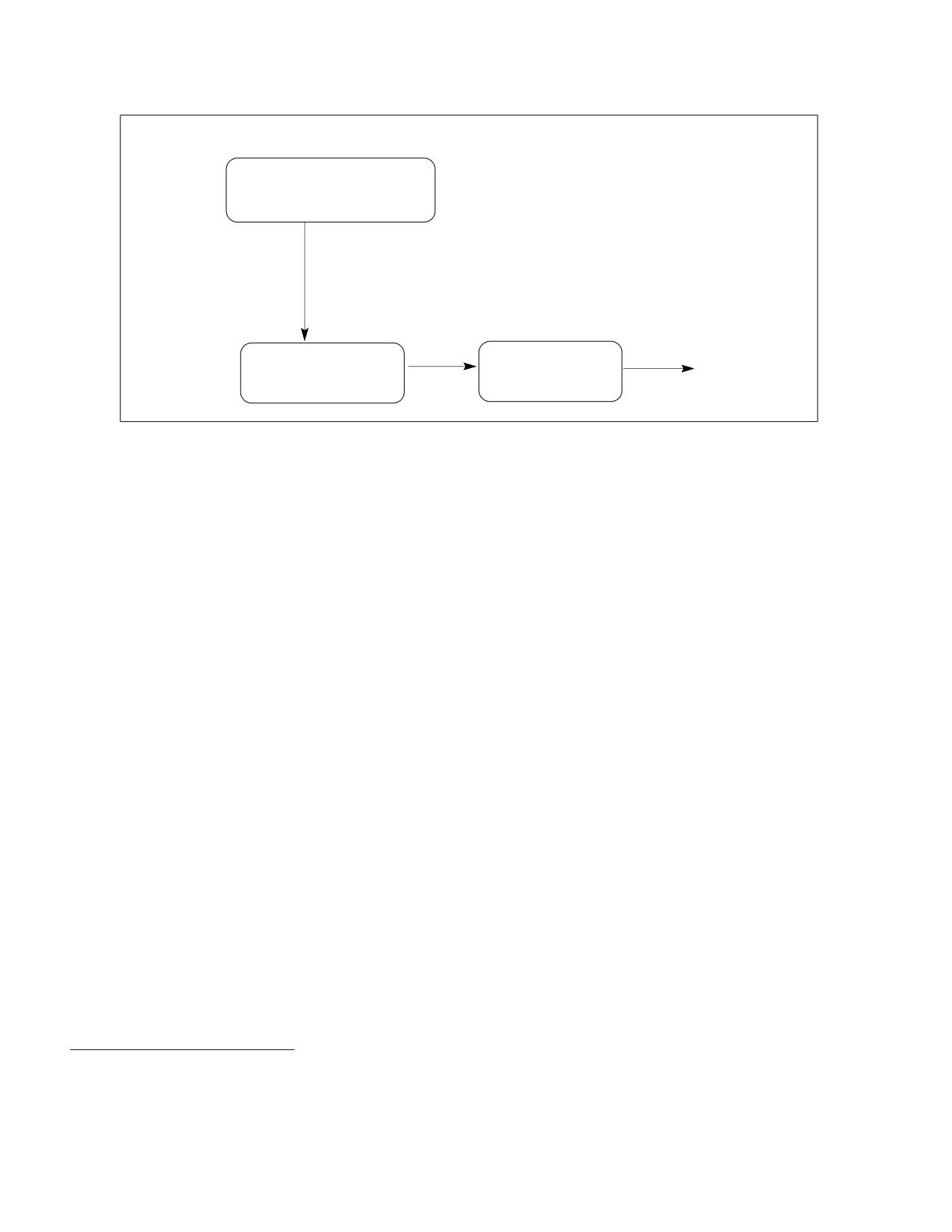
PROGRAMMING WITH INTEL® AVX-512
Check feature flag
CPUID.01H:ECX.OSXSAVE = 1?
OS provides processor
extended state management
Yes
Implied HW support for
XSAVE, XRSTOR, XGETBV, XCR0
Opmask,
YMM,ZMM
Check enabled state in
Check AVX512F flag
States
ok to use
XCR0 via XGETBV
enabled
Instructions
Figure 15-2. Procedural Flow for Application Detection of AVX-512 Foundation Instructions
Prior to using AVX-512 Foundation instructions, the application must identify that the operating system supports
the XGETBV instruction and the ZMM register state, in addition to confirming the processor’s support for ZMM state
management using XSAVE/XRSTOR and AVX-512 Foundation instructions. The following simplified sequence
accomplishes both and is strongly recommended.
1. Detect CPUID.01H:ECX.OSXSAVE[27] =1 (XGETBV enabled for application use1).
2. Execute XGETBV and verify that XCR0[7:5] = ‘111b’ (OPMASK state, upper 256-bit of ZMM0-ZMM15 and
ZMM16-ZMM31 state are enabled by OS) and that XCR0[2:1] = ‘11b’ (XMM state and YMM state are enabled by
OS).
3. Detect CPUID.07H.00H:EBX.AVX512F[16] = 1.
15.2.1 Additional 512-Bit Instruction Extensions of the Intel® AVX-512 Family
Processor support of the Intel AVX-512 Exponential and Reciprocal instructions are indicated by querying the
feature flag:
• If CPUID.07H.00H:EBX.AVX512_ER[27] = 1, the collection of VEXP2PD/VEXP2PS/VRCP28xx/VRSQRT28xx
instructions are supported.
Processor support of the Intel AVX-512 Prefetch instructions are indicated by querying the feature flag:
• If CPUID.07H.00H:EBX.AVX512_PF[26] = 1, a collection of VGATHERPF0xxx/VGATHERPF1xxx/VSCATTER-
PF0xxx/VSCATTERPF1xxx instructions are supported.
Detection of 512-bit instructions operating on ZMM states and opmask registers, outside of AVX-512 Foundation,
needs to follow the general procedural flow in Figure 15-3.
1. If CPUID.01H:ECX.OSXSAVE reports 1, it also indirectly implies the processor supports XSAVE, XRSTOR,
XGETBV, processor extended state bit vector XCR0 register. Thus an application may streamline the checking
of CPUID feature flags for XSAVE and OSXSAVE. XSETBV is a privileged instruction.
15-4
Vol. 1
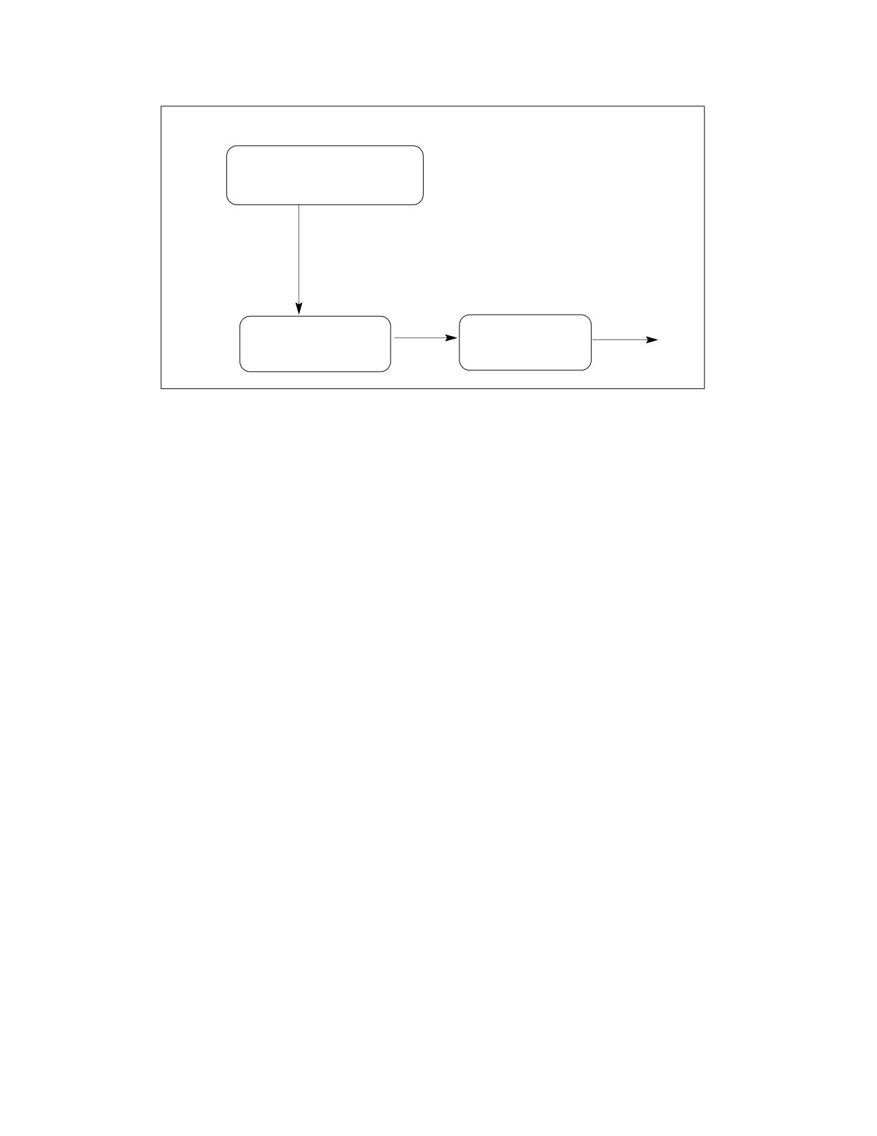
PROGRAMMING WITH INTEL® AVX-512
Check feature flag
CPUID.01H:ECX.OSXSAVE = 1?
OS provides processor
extended state management
Yes
Implied HW support for
XSAVE, XRSTOR, XGETBV, XCR0
Opmask,
YMM,ZMM
Check enabled state in
Check AVX512F and
States
additional 512-bit flags
ok to use
XCR0 via XGETBV
enabled
Instructions
Figure 15-3. Procedural Flow for Application Detection of 512-Bit Instructions
PREFETCHT1W does not require OS support for XMM/YMM/ZMM/k-reg, SIMD FP exception support.
Procedural Flow of Application Detection of other 512-bit extensions:
Prior to using the Intel AVX-512 Exponential and Reciprocal instructions, the application must identify that the
operating system supports the XGETBV instruction and the ZMM register state, in addition to confirming the
processor’s support for ZMM state management using XSAVE/XRSTOR and AVX-512 Foundation instructions. The
following simplified sequence accomplishes both and is strongly recommended.
1. Detect CPUID.01H:ECX.OSXSAVE[27] = 1 (XGETBV enabled for application use).
2. Execute XGETBV and verify that XCR0[7:5] = ‘111b’ (OPMASK state, upper 256-bit of ZMM0-ZMM15 and
ZMM16-ZMM31 state are enabled by OS) and that XCR0[2:1] = ‘11b’ (XMM state and YMM state are enabled
by OS).
3. Verify both CPUID.07H.00H:EBX.AVX512F[16] = 1, and CPUID.07H.00H:EBX.AVX512_ER[27] = 1.
Prior to using the Intel AVX-512 Prefetch instructions, the application must identify that the operating system
supports the XGETBV instruction and the ZMM register state, in addition to confirming the processor’s support for
ZMM state management using XSAVE/XRSTOR and AVX-512 Foundation instructions. The following simplified
sequence accomplishes both and is strongly recommended.
1. Detect CPUID.01H:ECX.OSXSAVE[27] = 1 (XGETBV enabled for application use).
2. Execute XGETBV and verify that XCR0[7:5] = ‘111b’ (OPMASK state, upper 256-bit of ZMM0-ZMM15 and
ZMM16-ZMM31 state are enabled by OS) and that XCR0[2:1] = ‘11b’ (XMM state and YMM state are enabled
by OS).
3. Verify both CPUID.07H.00H:EBX.AVX512F[16] = 1, and CPUID.07H.00H:EBX.AVX512_PF[26] = 1.
15.2.2 Detection of AVX512-FP16 Instructions
The AVX512-FP16 ISA extensions require that the AVX512BW feature be implemented since the instructions for
manipulating 32b masks are associated with AVX512BW.
Vol. 1
15-5
PROGRAMMING WITH INTEL® AVX-512
15.3
DETECTION OF 512-BIT INSTRUCTION GROUPS OF THE INTEL® AVX-512
FAMILY
In addition to the Intel AVX-512 Foundation instructions, the Intel AVX-512 family provides several groups of
instruction extensions that can operate in vector lengths of 512/256/128 bits. Each group is enumerated by a
CPUID.07H feature flag and can be encoded via the EVEX.L’L field to support operation at vector lengths smaller
than 512 bits. These instruction groups are listed in Table 15-1.
Table 15-1. 512-Bit Instruction Groups in the Intel® AVX-512 Family
CPUID.07H Feature Flag Bit
Feature Flag Abbreviation of 512-Bit Instruction Group
SW Detection Flow
CPUID.07H.00H:EBX[16]
AVX512F (AVX-512 Foundation)
Figure 15-2
CPUID.07H.00H:EBX[28]
AVX512CD
Figure 15-4
CPUID.07H.00H:EBX[17]
AVX512DQ
Figure 15-4
CPUID.07H.00H:EBX[30]
AVX512BW
Figure 15-4
Software must follow the detection procedure for the 512-bit AVX-512 Foundation instructions as described in
Section 15.2.
Detection of other 512-bit sibling instruction groups listed in Table 15-1 (excluding AVX512F) follows the procedure
described in Figure 15-4.
Check feature flag
CPUID.01H:ECX.OXSAVE = 1?
OS provides processor
extended state management
Yes
Implied HW support for
XSAVE, XRSTOR, XGETBV, XCR0
Opmask,
YMM,ZMM
Check enabled state in
Check AVX512F and
States
a sibling 512-bit flag
ok to use
XCR0 via XGETBV
enabled
Instructions
Figure 15-4. Procedural Flow for Application Detection of 512-Bit Instruction Groups
To detect 512-bit instructions enumerated by AVX512CD, the following sequence is strongly recommended.
1. Detect CPUID.01H:ECX.OSXSAVE[27] = 1 (XGETBV enabled for application use).
2. Execute XGETBV and verify that XCR0[7:5] = ‘111b’ (OPMASK state, upper 256-bit of ZMM0-ZMM15 and
ZMM16-ZMM31 state are enabled by OS) and that XCR0[2:1] = ‘11b’ (XMM state and YMM state are enabled by
OS).
3. Verify both CPUID.07H.00H:EBX.AVX512F[16] = 1, CPUID.07H.00H:EBX.AVX512CD[28] = 1.
Similarly, the detection procedure for enumerating 512-bit instructions reported by AVX512DW follows the same
flow.
15-6
Vol. 1
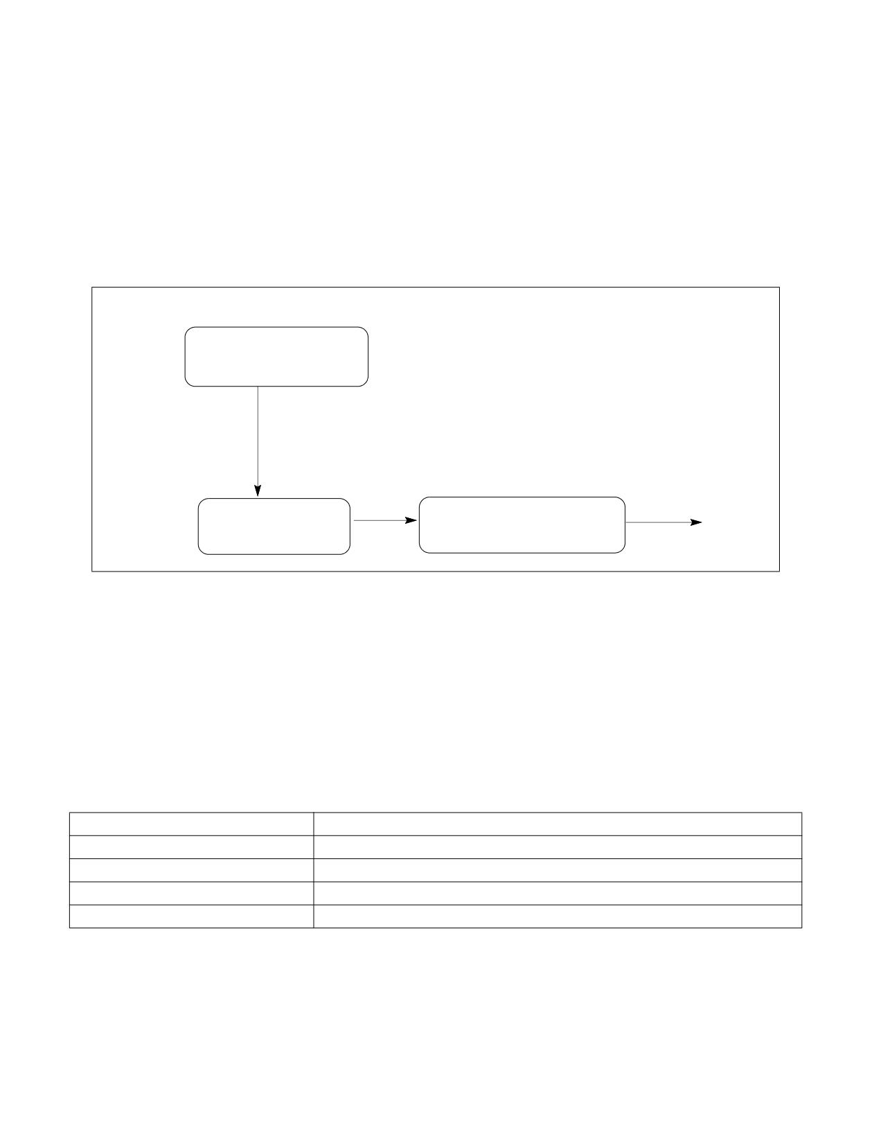
PROGRAMMING WITH INTEL® AVX-512
15.4
DETECTION OF INTEL® AVX-512 INSTRUCTION GROUPS OPERATING AT
256 AND 128-BIT VECTOR LENGTHS
For each of the 512-bit instruction groups in the Intel AVX-512 family listed in Table 15-1, the EVEX encoding
scheme may support a vast majority of these instructions operating at 256-bit or 128-bit (if applicable) vector
lengths. Encoding support for vector lengths smaller than 512-bits is indicated by CPUID.07H.00H:EBX[31],
abbreviated as AVX512VL.
The AVX512VL flag alone is never sufficient to determine a given Intel AVX-512 instruction may be encoded at
vector lengths smaller than 512 bits. Software must use the procedure described in Figure 15-5 and Table 15-2.
Check feature flag
CPUID.01H:ECX.OXSAVE = 1?
OS provides processor
extended state management
Yes
Implied HW support for
XSAVE, XRSTOR, XGETBV, XCR0
Opmask,
YMM,ZMM
Check enabled state in
Check applicable collection of
States
CPUID flags listed in Table 2-2
ok to use
XCR0 via XGETBV
enabled
Instructions
Figure 15-5. Procedural Flow for Detection of Intel® AVX-512 Instructions Operating at Vector Lengths < 512
To illustrate the procedure described in Figure 15-5 and Table 15-2 for software to use EVEX.256 encoded VPCON-
FLICT, the following sequence is provided. It is strongly recommended this sequence is followed.
1) Detect CPUID.01H:ECX.OSXSAVE[27] = 1 (XGETBV enabled for application use).
2) Execute XGETBV and verify that XCR0[7:5] = ‘111b’ (OPMASK state, upper 256-bit of ZMM0-ZMM15 and
ZMM16-ZMM31 state are enabled by OS) and that XCR0[2:1] = ‘11b’ (XMM state and YMM state are enabled by
OS).
3) Verify CPUID.07H.00H:EBX.AVX512F[16] = 1, CPUID.07H.00H:EBX.AVX512CD[28] = 1, and
CPUID.07H.00H:EBX.AVX512VL[31] = 1.
Table 15-2. Feature Flag Collection Required of 256/128 Bit Vector Lengths for Each Instruction Group
Usage of 256/128 Vector Lengths
Feature Flag Collection to Verify
AVX512F
AVX512F & AVX512VL
AVX512CD
AVX512F & AVX512CD & AVX512VL
AVX512DQ
AVX512F & AVX512DQ & AVX512VL
AVX512BW
AVX512F & AVX512BW & AVX512VL
In some specific cases, AVX512VL may only support EVEX.256 encoding but not EVEX.128. These cases are listed
in Table 15-3.
Vol. 1
15-7

PROGRAMMING WITH INTEL® AVX-512
Table 15-3. Instruction Mnemonics That Do Not Support EVEX.128 Encoding
Instruction Group
Instruction Mnemonics Supporting EVEX.256 Only Using AVX512VL
VBROADCASTSD, VBROADCASTF32X4, VEXTRACTI32X4, VINSERTF32X4, VINSERTI32X4, VPERMD, VPER-
AVX512F
MPD, VPERMPS, VPERMQ, VSHUFF32X4, VSHUFF64X2, VSHUFI32X4, VSHUFI64X2
AVX512CD
VBROADCASTF32X2, VBROADCASTF64X2, VBROADCASTI32X4, VBROADCASTI64X2, VEXTRACTI64X2,
AVX512DQ
VINSERTF64X2, VINSERTI64X2,
AVX512BW
15.5
ACCESSING XMM, YMM, AND ZMM REGISTERS
The lower 128 bits of a YMM register is aliased to the corresponding XMM register. Legacy SSE instructions (i.e.,
SIMD instructions operating on XMM state but not using the VEX prefix, also referred to non-VEX encoded SIMD
instructions) will not access the upper bits (MAXVL-1:128) of the YMM registers. AVX and FMA instructions with a
VEX prefix and vector length of 128-bits zeroes the upper 128 bits of the YMM register.
Upper bits of YMM registers (255:128) can be read and written to by many instructions with a VEX.256 prefix.
XSAVE and XRSTOR may be used to save and restore the upper bits of the YMM registers.
The lower 256 bits of a ZMM register are aliased to the corresponding YMM register. Legacy SSE instructions (i.e.,
SIMD instructions operating on XMM state but not using the VEX prefix, also referred to non-VEX encoded SIMD
instructions) will not access the upper bits (MAXVL-1:128) of the ZMM registers, where MAXVL is maximum vector
length (currently 512 bits). AVX and FMA instructions with a VEX prefix and vector length of 128-bits zero the upper
384 bits of the ZMM register, while the VEX prefix and vector length of 256-bits zeroes the upper 256 bits of the
ZMM register.
Upper bits of ZMM registers (511:256) can be read and written to by instructions with an EVEX.512 prefix.
15.6
ENHANCED VECTOR PROGRAMMING ENVIRONMENT USING EVEX
ENCODING
EVEX-encoded AVX-512 instructions support an enhanced vector programming environment. The enhanced vector
programming environment uses the combination of EVEX bit-field encodings and a set of eight opmask registers to
provide the following capabilities:
• Conditional vector processing of an EVEX-encoded instruction. Opmask registers k1 through k7 can be used to
conditionally govern the per-data-element computational operation and the per-element updates to the
destination operand of an AVX-512 Foundation instruction. Each bit of the opmask register governs one vector
element operation (a vector element can be 8 bits, 16 bits, 32 bits or 64 bits).
• In addition to providing predication control on vector instructions via EVEX bit-field encoding, the opmask
registers can also be used similarly on general-purpose registers as source/destination operands using modR/M
encoding for non-mask-related instructions. In this case, an opmask register k0 through k7 can be selected.
• In 64-bit mode, 32 vector registers can be encoded using the EVEX prefix.
• Broadcast may be supported for some instructions on the operand that can be encoded as a memory vector.
The data elements of a memory vector may be conditionally fetched or written to, and the vector size is
dependent on the data transformation function.
• Flexible rounding control for the register-to-register flavor of EVEX encoded 512-bit and scalar instructions.
Four rounding modes are supported by direct encoding within the EVEX prefix, overriding MXCSR settings.
• Broadcast of one element to the rest of the destination vector register.
• Compressed 8-bit displacement encoding scheme to increase the instruction encoding density for instructions
that normally require disp32 syntax.
15-8
Vol. 1
PROGRAMMING WITH INTEL® AVX-512
15.6.1 OPMASK Register to Predicate Vector Data Processing
AVX-512 instructions using EVEX encode a predicate operand to conditionally control per-element computational
operation and updating of the result to the destination operand. The predicate operand is known as the opmask
register. The opmask is a set of eight architectural registers of size MAX_KL (64-bit). Note that from this set of eight
architectural registers, only k1 through k7 can be addressed as a predicate operand. k0 can be used as a regular
source or destination but cannot be encoded as a predicate operand. Note also that a predicate operand can be
used to enable memory fault-suppression for some instructions with a memory operand (source or destination).
As a predicate operand, the opmask registers contain one bit to govern the operation/update to each data element
of a vector register. In general, opmask registers can support instructions with all element sizes: byte (int8), word
(int16), single precision floating-point (float32), integer doubleword (int32), double precision floating-point
(float64), integer quadword (int64). Therefore, a ZMM vector register can hold 8, 16, 32, or 64 elements in prin-
ciple. The length of an opmask register, MAX_KL, is sufficient to handle up to 64 elements with one bit per element,
i.e., 64 bits. Masking is supported in most of the AVX-512 instructions. For a given vector length, each instruction
accesses only the number of least significant mask bits that are needed based on its data type. For example, AVX-
512 Foundation instructions operating on 64-bit data elements with a 512-bit vector length, only use the 8 least
significant bits of the opmask register.
An opmask register affects an AVX-512 instruction at per-element granularity. Any numeric or non-numeric oper-
ation of each data element and per-element updates of intermediate results to the destination operand are predi-
cated on the corresponding bit of the opmask register.
An opmask serving as a predicate operand in AVX-512 obeys the following properties:
• The instruction’s operation is not performed for an element if the corresponding opmask bit is not set. This
implies that no exception or violation can be caused by an operation on a masked-off element. Consequently,
no MXCSR exception flag is updated as a result of a masked-off operation.
• A destination element is not updated with the result of the operation if the corresponding writemask bit is not
set. Instead, the destination element value must be preserved (merging-masking) or it must be zeroed out
(zeroing-masking).
• For some instructions with a memory operand, memory faults are suppressed for elements with a mask bit of
0.
Note that this feature provides a versatile construct to implement control-flow predication as the mask in effect
provides a merging behavior for AVX-512 vector register destinations. As an alternative the masking can be used
for zeroing instead of merging, so that the masked out elements are updated with 0 instead of preserving the old
value. The zeroing behavior is provided to remove the implicit dependency on the old value when it is not needed.
Most instructions with masking enabled accept both forms of masking. Instructions that must have EVEX.aaa bits
different than 0 (gather and scatter) and instructions that write to memory only accept merging-masking.
It’s important to note that the per-element destination update rule also applies when the destination operand is a
memory location. Vectors are written on a per element basis, based on the opmask register used as a predicate
operand.
The value of an opmask register can be:
• Generated as a result of a vector instruction (e.g., CMP, FPCLASS, etc.).
• Loaded from memory.
• Loaded from a GPR register.
• Modified by mask-to-mask operations.
Opmask registers can be used for purposes outside of predication. For example, they can be used to manipulate
sparse sets of elements from a vector, or used to set the EFLAGS based on the 0/0xFFFFFFFFFFFFFFFF/other status
of the OR of two opmask registers.
15.6.1.1 Opmask Register K0
The only exception to the opmask rules described above is that opmask k0 cannot be used as a predicate operand.
Opmask k0 cannot be encoded as a predicate operand for a vector operation; the encoding value that would select
opmask k0 will instead select an implicit opmask value of 0xFFFFFFFFFFFFFFFF, thereby effectively disabling
Vol. 1
15-9
PROGRAMMING WITH INTEL® AVX-512
masking. Opmask register k0 can still be used for any instruction that takes opmask register(s) as operand(s)
(either source or destination).
Note that certain instructions implicitly use the opmask as an extra destination operand. In such cases, trying to
use the “no mask” feature will translate into a #UD fault being raised.
15.6.1.2 Example of Opmask Usages
The example below illustrates the predicated vector add operation and predicated updates of added results into the
destination operand. The initial state of vector registers zmm0, zmm1, and zmm2 and k3 are:
MSB
LSB
zmm0 =
[ 0x00000003 0x00000002 0x00000001 0x00000000 ] (bytes 15 through 0)
[ 0x00000007 0x00000006 0x00000005 0x00000004 ] (bytes 31 through 16)
[ 0x0000000B 0x0000000A 0x00000009 0x00000008 ] (bytes 47 through 32)
[ 0x0000000F 0x0000000E 0x0000000D 0x0000000C ] (bytes 63 through 48)
zmm1 =
[ 0x0000000F 0x0000000F 0x0000000F 0x0000000F ] (bytes 15 through 0)
[ 0x0000000F 0x0000000F 0x0000000F 0x0000000F ] (bytes 31 through 16)
[ 0x0000000F 0x0000000F 0x0000000F 0x0000000F ] (bytes 47 through 32)
[ 0x0000000F 0x0000000F 0x0000000F 0x0000000F ] (bytes 63 through 48)
zmm2 =
[ 0xAAAAAAAA 0xAAAAAAAA 0xAAAAAAAA 0xAAAAAAAA ] (bytes 15 through 0)
[ 0xBBBBBBBB 0xBBBBBBBB 0xBBBBBBBB 0xBBBBBBBB ] (bytes 31 through 16)
[ 0xCCCCCCCC 0xCCCCCCCC 0xCCCCCCCC 0xCCCCCCCC ] (bytes 47 through 32)
[ 0xDDDDDDDD 0xDDDDDDDD 0xDDDDDDDD 0xDDDDDDDD ] (bytes 63 through 48)
k3 = 0x8F03 (1000 1111 0000 0011)
An opmask register serving as a predicate operand is expressed as a curly-braces-enclosed decorator following the
first operand in the Intel assembly syntax. Given this state, we will execute the following instruction:
vpaddd zmm2 {k3}, zmm0, zmm1
The vpaddd instruction performs 32-bit integer additions on each data element conditionally based on the corre-
sponding bit value in the predicate operand k3. Since per-element operations are not operated if the corresponding
bit of the predicate mask is not set, the intermediate result is:
[ ********** ********** 0x00000010 0x0000000F ] (bytes 15 through 0)
[ ********** ********** ********** ********** ] (bytes 31 through 16)
[ 0x0000001A 0x00000019 0x00000018 0x00000017 ] (bytes 47 through 32)
[ 0x0000001E ********** ********** ********** ] (bytes 63 through 48)
where ”**********” indicates that no operation is performed.
This intermediate result is then written into the destination vector register, zmm2, using the opmask register k3 as
the writemask, producing the following final result:
15-10
Vol. 1
PROGRAMMING WITH INTEL® AVX-512
zmm2 =
[ 0xAAAAAAAA 0xAAAAAAAA 0x00000010 0x0000000F ] (bytes 15 through 0)
[ 0xBBBBBBBB 0xBBBBBBBB 0xBBBBBBBB 0xBBBBBBBB ] (bytes 31 through 16)
[ 0x0000001A 0x00000019 0x00000018 0x00000017 ] (bytes 47 through 32)
[ 0x0000001E 0xDDDDDDDD 0xDDDDDDDD 0xDDDDDDDD ] (bytes 63 through 48)
Note that for a 64-bit instruction (for example, vaddpd), only the 8 LSB of mask k3 (0x03) would be used to iden-
tify the predicate operation on each one of the 8 elements of the source/destination vectors.
15.6.2 OpMask Instructions
AVX-512 Foundation instructions provide a collection of opmask instructions that allow programmers to set, copy,
or operate on the contents of a given opmask register. There are three types of opmask instructions:
• Mask read/write instructions: These instructions move data between a general-purpose integer register or
memory and an opmask mask register, or between two opmask registers. For example:
- kmovw k1, ebx; move lower 16 bits of ebx to k1.
• Flag instructions: This category consists of instructions that modify EFLAGS based on the content of opmask
registers.
- kortestw k1, k2; OR registers k1 and k2 and updated EFLAGS accordingly.
• Mask logical instructions: These instructions perform standard bitwise logical operations between opmask
registers.
- kandw k1, k2, k3; AND lowest 16 bits of registers k2 and k3, leaving the result in k1.
15.6.3 Broadcast
EVEX encoding provides a bit-field to encode data broadcast for some load-op instructions, i.e., instructions that
load data from memory and perform some computational or data movement operation. A source element from
memory can be broadcasted (repeated) across all the elements of the effective source operand (up to 16 times for
a 32-bit data element, up to 8 times for a 64-bit data element). This is useful when reusing the same scalar
operand for all the operations in a vector instruction. Note that some processors may perform multiple loads of the
source element and thus software should not rely on atomicity of the data being broadcast (e.g., when the source
element is simultaneously modified by another logical processor).
Broadcast is only enabled on instructions with an element size of 32 bits or 64 bits. Byte and word instructions do
not support embedded broadcast.
The functionality of data broadcast is expressed as a curly-braces-enclosed decorator following the last
register/memory operand in the Intel assembly syntax.
For instance:
vmulps zmm1, zmm2, [rax] {1to16}
The {1to16} primitive loads one float32 (single precision) element from memory, replicates it 16 times to form a
vector of 16 32-bit floating-point elements, multiplies the 16 float32 elements with the corresponding elements in
the first source operand vector, and puts each of the 16 results into the destination operand.
AVX-512 instructions with store semantics and pure load instructions do not support broadcast primitives.
vmovaps [rax] {k3}, zmm19
Vol. 1
15-11

PROGRAMMING WITH INTEL® AVX-512
In contrast, the k3 opmask register is used as the predicate operand in the above example. Only the store opera-
tion on data elements corresponding to the non-zero bits in k3 will be performed.
15.6.4 Static Rounding Mode and Suppress All Exceptions
In previous SIMD instruction extensions (up to AVX and AVX2), rounding control is generally specified in MXCSR,
with a handful of instructions providing per-instruction rounding override via encoding fields within the imm8
operand. AVX-512 offers a more flexible encoding attribute to override MXCSR-based rounding control for floating-
pointing instructions with rounding semantics. This rounding attribute embedded in the EVEX prefix is called Static
(per instruction) Rounding Mode or Rounding Mode override. This attribute allows programmers to statically apply
a specific arithmetic rounding mode irrespective of the value of RM bits in MXCSR. It is available only to register-to-
register flavors of EVEX-encoded floating-point instructions with rounding semantic. The differences between these
three rounding control interfaces are summarized in Table 15-4.
Table 15-4. Characteristics of Three Rounding Control Interfaces
Static Rounding
Imm8 Embedded Rounding
Rounding Interface
MXCSR Rounding Control
Override
Override
Semantic Requirement
FP rounding
FP rounding
FP rounding
Prefix Requirement
EVEX.B = 1
NA
NA
Rounding Control
EVEX.L’L
IMM8[1:0] or MXCSR.RC
MXCSR.RC
(depending on IMM8[2])
Suppress All Exceptions (SAE)
Implied
no
no
SIMD FP Exception #XM
All suppressed
Can raise #I, #P (unless SPE is set)
MXCSR masking controls
MXCSR flag update
No
yes (except PE if SPE is set)
Yes
Precedence
Above MXCSR.RC
Above EVEX.L’L
Default
Scope
512-bit, reg-reg,
ROUNDPx, ROUNDSx,
All SIMD operands, vector lengths
Scalar reg-reg
VCVTPS2PH, VRNDSCALExx
The static rounding-mode override in Intel AVX-512 also implies the “suppress-all-exceptions” (SAE) attribute. The
SAE effect is as if all the MXCSR mask bits are set, and none of the MXCSR flags will be updated. Using static
rounding-mode via EVEX without SAE is not supported.
Static Rounding Mode and SAE control can be enabled in the encoding of the instruction by setting the EVEX.b bit
to 1 in a register-register vector instruction. In such a case, vector length is assumed to be MAXVL (512-bit in case
of AVX-512 packed vector instructions) or 128-bit for scalar instructions. Table 15-5 summarizes the possible static
rounding-mode assignments in AVX-512 instructions.
Note that some instructions already allow specifying the rounding mode statically via immediate bits. In such
cases, the immediate bits take precedence over the embedded rounding mode (in the same vein that they take
precedence over whatever MXCSR.RM says).
Table 15-5. Static Rounding Mode
Function
Description
{rn-sae}
Round to nearest (even) + SAE
{rd-sae}
Round down (toward -inf) + SAE
{ru-sae}
Round up (toward +inf) + SAE
{rz-sae}
Round toward zero (Truncate) + SAE
An example of use would be as follows:
vaddps zmm7 {k6}, zmm2, zmm4, {rd-sae}
15-12
Vol. 1
PROGRAMMING WITH INTEL® AVX-512
This would perform the single precision floating-point addition of vectors zmm2 and zmm4 with round-towards-
minus-infinity, leaving the result in vector zmm7 using k6 as conditional writemask.
Note that MXCSR.RM bits are ignored and unaffected by the outcome of this instruction.
Examples of instruction instances where the static rounding-mode is not allowed are shown below:
; rounding-mode already specified in the instruction immediate
vrndscaleps zmm7 {k6}, zmm2, 0x00
; instructions with memory operands
vmulps zmm7 {k6}, zmm2,[rax], {rd-sae}
; instructions with vector length different than MAXVL (512-bit)
vaddps ymm7 {k6}, ymm2, ymm4,{rd-sae}
15.6.5 Compressed Disp8*N Encoding
EVEX encoding supports a new displacement representation that allows for a more compact encoding of memory
addressing commonly used in unrolled code, where an 8-bit displacement can address a range exceeding the
dynamic range of an 8-bit value. This compressed displacement encoding is referred to as disp8*N, where N is a
constant implied by the memory operation characteristic of each instruction.
The compressed displacement is based on the assumption that the effective displacement (of a memory operand
occurring in a loop) is a multiple of the granularity of the memory access of each iteration. Since the base register
in memory addressing already provides byte-granular resolution, the lower bits of the traditional disp8 operand
become redundant, and can be implied from the memory operation characteristic.
The memory operation characteristics depend on the following:
• The destination operand is updated as a full vector, a single element, or multi-element tuples.
• The memory source operand (or vector source operand if the destination operand is memory) is fetched (or
treated) as a full vector, a single element, or multi-element tuples.
For example:
vaddps zmm7, zmm2, disp8[membase + index*8]
The destination zmm7 is updated as a full 512-bit vector, and 64-bytes of data are fetched from memory as a full
vector; the next unrolled iteration may fetch from memory in 64-byte granularity per iteration. There are 6 bits of
lowest address that can be compressed, hence N = 2^6 = 64. The contribution of “disp8” to effective address
calculation is 64*disp8.
vbroadcastf32x4 zmm7, disp8[membase + index*8]
In VBROADCASTF32x4, memory is fetched as a 4tuple of 4 32-bit entities. Hence the common lowest address bits
that can be compressed are 4, corresponding to the 4tuple width of 2^4 = 16 bytes (4x32 bits). Therefore, N =
2^4.
For EVEX encoded instructions that update only one element in the destination, or the source element is fetched
individually, the number of lowest address bits that can be compressed is generally the width in bytes of the data
element, hence N = 2^(width).
15.7
MEMORY ALIGNMENT
Memory alignment requirements on EVEX-encoded SIMD instructions are similar to VEX-encoded SIMD instruc-
tions. Memory alignment applies to EVEX-encoded SIMD instructions in three categories:
• Explicitly-aligned SIMD load and store instructions accessing 64 bytes of memory with EVEX prefix encoded
vector length of 512 bits (e.g., VMOVAPD, VMOVAPS, VMOVDQA, etc.). These instructions always require the
memory address to be aligned on a 64-byte boundary.
Vol. 1
15-13

PROGRAMMING WITH INTEL® AVX-512
• Explicitly-unaligned SIMD load and store instructions accessing 64 bytes or less of data from memory (e.g.,
VMOVUPD, VMOVUPS, VMOVDQU, VMOVQ, VMOVD, etc.). These instructions do not require the memory
address to be aligned on a natural vector-length byte boundary.
• Most arithmetic and data processing instructions encoded using EVEX support memory access semantics.
When these instructions access from memory, there are no alignment restrictions.
Software may see performance penalties when unaligned accesses cross cacheline boundaries or vector-length
naturally-aligned boundaries, so reasonable attempts to align commonly used data sets should continue to be
pursued.
Atomic memory operation in Intel 64 and IA-32 architecture is guaranteed only for a subset of memory operand
sizes and alignment scenarios. The guaranteed atomic operations are described in Section 11.1.1, “Guaranteed
Atomic Operations,” of the Intel® 64 and IA-32 Architectures Software Developer’s Manual, Volume 3A. Intel AVX
and FMA instructions do not introduce any new guaranteed atomic memory operations.
Intel AVX-512 instructions may generate an #AC(0) fault on misaligned 4 or 8-byte memory references in Ring-3
when CR0.AM=1. 16, 32, and 64-byte memory references will not generate an #AC(0) fault. See Table 15-7 for
details.
Certain AVX-512 Foundation instructions always require 64-byte alignment (see the complete list of VEX and EVEX
encoded instructions in Table 15-6). These instructions will #GP(0) if not aligned to 64-byte boundaries.
Table 15-6. SIMD Instructions Requiring Explicitly Aligned Memory
Require 16-byte alignment
Require 32-byte alignment
Require 64-byte alignment*
(V)MOVDQA xmm, m128
VMOVDQA ymm, m256
VMOVDQA zmm, m512
(V)MOVDQA m128, xmm
VMOVDQA m256, ymm
VMOVDQA m512, zmm
(V)MOVAPS xmm, m128
VMOVAPS ymm, m256
VMOVAPS zmm, m512
(V)MOVAPS m128, xmm
VMOVAPS m256, ymm
VMOVAPS m512, zmm
(V)MOVAPD xmm, m128
VMOVAPD ymm, m256
VMOVAPD zmm, m512
(V)MOVAPD m128, xmm
VMOVAPD m256, ymm
VMOVAPD m512, zmm
(V)MOVNTDQA xmm, m128
VMOVNTPS m256, ymm
VMOVNTPS m512, zmm
(V)MOVNTPS m128, xmm
VMOVNTPD m256, ymm
VMOVNTPD m512, zmm
(V)MOVNTPD m128, xmm
VMOVNTDQ m256, ymm
VMOVNTDQ m512, zmm
(V)MOVNTDQ m128, xmm
VMOVNTDQA ymm, m256
VMOVNTDQA zmm, m512
Table 15-7. Instructions Not Requiring Explicit Memory Alignment
(V)MOVDQU xmm, m128
VMOVDQU ymm, m256
VMOVDQU zmm, m512
(V)MOVDQU m128, m128
VMOVDQU m256, ymm
VMOVDQU m512, zmm
(V)MOVUPS xmm, m128
VMOVUPS ymm, m256
VMOVUPS zmm, m512
(V)MOVUPS m128, xmm
VMOVUPS m256, ymm
VMOVUPS m512, zmm
(V)MOVUPD xmm, m128
VMOVUPD ymm, m256
VMOVUPD zmm, m512
(V)MOVUPD m128, xmm
VMOVUPD m256, ymm
VMOVUPD m512, zmm
15.8
SIMD FLOATING-POINT EXCEPTIONS
AVX-512 instructions can generate SIMD floating-point exceptions (#XM) if embedded “suppress all exceptions”
(SAE) in EVEX is not set. When SAE is not set, these instructions will respond to exception masks of MXCSR in the
same way as VEX-encoded AVX instructions. When CR4.OSXMMEXCPT=0, any unmasked FP exceptions generate
an Undefined Opcode exception (#UD).
15-14
Vol. 1
PROGRAMMING WITH INTEL® AVX-512
15.9
INSTRUCTION EXCEPTION SPECIFICATION
Exception behavior of VEX-encoded Intel AVX and Intel AVX2 instructions are described in the Intel® 64 and IA-32
Architectures Software Developer’s Manual, Volume 2A. Exception behavior of Intel AVX-512 Foundation instruc-
tions and additional 512-bit extensions are described in Section 2.8, “Exception Classifications of EVEX-Encoded
instructions,” and Section 2.9, “Exception Classifications of Opmask instructions, Type K20 and Type K21.”
15.10 EMULATION
Setting the CR0.EM bit to 1 provides a technique to emulate legacy Intel SSE floating-point instruction sets in soft-
ware. This technique is not supported with Intel AVX instructions, nor FMA instructions.
If an operating system wishes to emulate Intel AVX instructions, set XCR0[2:1] to zero. This will cause Intel AVX
instructions to #UD. Emulation of FMA by the operating system can be done similarly as with emulating Intel AVX
instructions.
15.11 WRITING FLOATING-POINT EXCEPTION HANDLERS
Intel AVX-512, Intel AVX, and FMA floating-point exceptions are handled in an entirely analogous way to legacy
SSE floating-point exceptions. To handle unmasked SIMD floating-point exceptions, the operating system or exec-
utive must provide an exception handler. Section 11.5.1, “SIMD Floating-Point Exceptions,” describes the SIMD
floating-point exception classes and gives suggestions for writing an exception handler to handle them.
To indicate that the operating system provides a handler for SIMD floating-point exceptions (#XM), the
CR4.OSXMMEXCPT flag (bit 10) must be set.
Vol. 1
15-15
PROGRAMMING WITH INTEL® AVX-512
15-16
Vol. 1

CHAPTER 16
PROGRAMMING WITH INTEL® AVX10
16.1
INTRODUCTION
Intel® Advanced Vector Extensions 10 (Intel® AVX10) represents an enhancement to Intel® Advanced Vector
Extensions 512 (Intel® AVX-512). Intel AVX10 establishes a common, converged vector instruction set across all
Intel architectures, incorporating the modern vectorization aspects of Intel AVX-512.
Intel AVX10 is based on Intel AVX-512 and includes all Intel AVX-512 instructions. It supports all instruction vector
lengths (128, 256, and 512), as well as scalar and opmask instructions.
16.2
FEATURE VERSIONING AND ENUMERATION
Most Intel AVX10 instructions and features will be organized in collections called versions. In some situations, a
processor may introduce AVX10 instructions that are not part of that processor’s AVX10 version. Such instructions
will be enumerated discretely (see below).
AVX10 versions support enumeration that is monotonically increasing and inclusive. This can simplify application
development by ensuring that all Intel processors support the same features and instructions at a given Intel
AVX10 version number, as well as reduce the number of CPUID feature flags required to be checked by an applica-
tion to determine feature support. In this enumeration paradigm, the application developer only need to check a
CPUID feature flag indicating that the Intel AVX10 ISA is supported and a version number to ensure that the
supported version is greater than or equal to the desired version.
The AVX10 feature flag indicates processor support for Intel AVX10 and the presence of a “Converged Vector ISA”
leaf containing a field for the version number. AVX10 features or instructions that are not part of an AVX10 version
when they are introduced will be enumerated with a discrete feature flag in that CPUID leaf. See Table 16-1 for
details.
Table 16-1. CPUID Enumeration of Intel® AVX10
CPUID Bit
Description
Type
CPUID.07H.01H:EDX[19]
If 1, Intel® AVX10 is supported.
Bit (0/1)
CPUID.24H.00H:EAX[31:0]
Reports the maximum supported sub-leaf.
Integer
CPUID.24H.00H:EBX[7:0]
Reports the Intel AVX10 version.
Integer (≥ 1)
CPUID.24H.00H:EBX[15:8]
Reserved.
N/A
CPUID.24H.00H:EBX[18:16]
Reserved.
Always 111B1
CPUID.24H.00H:EBX[31:19]
Reserved.
N/A
CPUID.24H.00H:ECX[31:0]
Reserved.
N/A
CPUID.24H.00H:EDX[31:0]
Reserved.
N/A
CPUID.24H.01H:EAX[31:0]
Reserved for discrete feature bits.
N/A
CPUID.24H.01H:EBX[31:0]
Reserved for discrete feature bits.
N/A
CPUID.24H.01H:ECX[31:0]
Reserved for discrete feature bits.
N/A
CPUID.24H.01H:EDX[31:0]
Reserved for discrete feature bits.
N/A
NOTES:
1. Earlier versions of this specification documented these bits as enumerating support for different vector lengths. Processors enumer-
ating Intel® AVX10 support all vector widths.
Several important principles of Intel AVX10 enumeration are the following:
Vol. 1
16-1

PROGRAMMING WITH INTEL® AVX10
• Versions will be inclusive such that version N+1 is a superset of version N. Once an instruction is introduced in
Intel AVX10.x, it is expected to be carried forward in all subsequent Intel AVX10 versions, allowing a developer
to check only for a version greater than or equal to the desired version.
• Any processor that enumerates support for Intel AVX10 will also enumerate support for Intel AVX, Intel AVX2,
and Intel AVX-512 (see Table 16-2).
The first version of Intel AVX10 (Version 1, or Intel® AVX10.1) supports the Intel AVX-512 instruction families
shown in Table 16-2.
Table 16-2. Intel® AVX-512 CPUID Feature Flags Included in Intel® AVX10
Feature Introduction
Intel® AVX-512 CPUID Feature Flags Included in Intel® AVX10
Intel® Xeon® Scalable Processor Family based on Skylake
AVX512F, AVX512CD, AVX512BW, AVX512DQ
microarchitecture
Intel® Core™ processors based on Cannon Lake microarchitecture
AVX512-VBMI, AVX512-IFMA
2nd generation Intel® Xeon® Scalable Processor Family based on
AVX512-VNNI
Cascade Lake product
3rd generation Intel® Xeon® Scalable Processor Family based on
AVX512-BF16
Cooper Lake product
3rd generation Intel® Xeon® Scalable Processor Family based on Ice
AVX512-VPOPCNTDQ, AVX512-VBMI2, VAES, GFNI,
Lake microarchitecture
VPCLMULQDQ, AVX512-BITALG
4th generation Intel® Xeon® Scalable Processor Family based on
AVX512-FP16
Sapphire Rapids microarchitecture
NOTE
VAES, VPCLMULQDQ, and GFNI EVEX instructions will be supported on Intel AVX10.1 machines but
will continue to be enumerated by their existing discrete CPUID feature flags. This requires the
developer to check for both the feature and Intel AVX10, e.g., {AVX10.1 AND VAES}.
New vector ISA features will only be added to the Intel AVX10 ISA moving forward.
16-2
Vol. 1
CHAPTER 17
PROGRAMMING WITH INTEL® TRANSACTIONAL SYNCHRONIZATION
EXTENSIONS
17.1
OVERVIEW
This chapter describes the software programming interface to the Intel® Transactional Synchronization Extensions
of the Intel 64 architecture.
Multi-threaded applications take advantage of increasing number of cores to achieve high performance. However,
writing multi-threaded applications requires programmers to reason about data sharing among multiple threads.
Access to shared data typically requires synchronization mechanisms. These mechanisms ensure multiple threads
update shared data by serializing operations on the shared data, often through the use of a critical section
protected by a lock. Since serialization limits concurrency, programmers try to limit synchronization overheads.
They do this either through minimizing the use of synchronization or through the use of fine-grain locks; where
multiple locks each protect different shared data. Unfortunately, this process is difficult and error prone; a missed
or incorrect synchronization can cause an application to fail. Conservatively adding synchronization and using
coarser granularity locks, where a few locks each protect many items of shared data, helps avoid correctness prob-
lems but limits performance due to excessive serialization. While programmers must use static information to
determine when to serialize, the determination as to whether actually to serialize is best done dynamically.
Intel® Transactional Synchronization Extensions aim to improve the performance of lock-protected critical sections
while maintaining the lock-based programming model.
17.2
INTEL® TRANSACTIONAL SYNCHRONIZATION EXTENSIONS
Intel® Transactional Synchronization Extensions (Intel® TSX) allow the processor to determine dynamically
whether threads need to serialize through lock-protected critical sections, and to perform serialization only when
required. This lets the hardware expose and exploit concurrency hidden in an application due to dynamically unnec-
essary synchronization through a technique known as lock elision.
With lock elision, the hardware executes the programmer-specified critical sections (also referred to as transac-
tional regions) transactionally. In such an execution, the lock variable is only read within the transactional region;
it is not written to (and therefore not acquired) with the expectation that the lock variable remains unchanged after
the transactional region, thus exposing concurrency.
If the transactional execution completes successfully, then the hardware ensures that all memory operations
performed within the transactional region will appear to have occurred instantaneously when viewed from other
logical processors, a process referred to as an atomic commit. Any updates performed within the transactional
region are made visible to other processors only on an atomic commit.
Since a successful transactional execution ensures an atomic commit, the processor can execute the programmer-
specified code section optimistically without synchronization. If synchronization was unnecessary for that specific
execution, execution can commit without any cross-thread serialization.
If the transactional execution is unsuccessful, the processor cannot commit the updates atomically. When this
happens, the processor will roll back the execution, a process referred to as a transactional abort. On a transac-
tional abort, the processor will discard all updates performed in the region, restore architectural state to appear as
if the optimistic execution never occurred, and resume execution non-transactionally. Depending on the policy in
place, lock elision may be retried or the lock may be explicitly acquired to ensure forward progress.
Intel TSX provides two software interfaces for programmers.
• Hardware Lock Elision (HLE) is a legacy compatible instruction set extension comprising the XACQUIRE and
XRELEASE prefixes.
• Restricted Transactional Memory (RTM) is an instruction set interface comprising the XBEGIN and XEND
instructions.
Vol. 1
17-1
PROGRAMMING WITH INTEL® TRANSACTIONAL SYNCHRONIZATION EXTENSIONS
Programmers who would like to run Intel TSX-enabled software on legacy hardware would use the HLE interface to
implement lock elision. On the other hand, programmers who do not have legacy hardware requirements and who
deal with more complex locking primitives would use the RTM software interface of Intel TSX to implement lock
elision. In the latter case when using new instructions, the programmer must always provide a non-transactional
path (which would have code to eventually acquire the lock being elided) to execute following a transactional abort
and must not rely on the transactional execution alone.
Intel TSX provides the XTEST instruction to test whether a logical processor is executing transactionally, and the
XABORT instruction to abort a transactional region.
A processor can perform a transactional abort for numerous reasons. A primary cause is due to conflicting accesses
between the transactionally executing logical processor and another logical processor. Such conflicting accesses
may prevent a successful transactional execution. Memory addresses read from within a transactional region
constitute the read-set of the transactional region and addresses written to within the transactional region consti-
tute the write-set of the transactional region. Intel TSX maintains the read- and write-sets at the granularity of a
cache line.
A conflicting data access occurs if another logical processor either reads a location that is part of the transactional
region’s write-set or writes a location that is a part of either the read- or write-set of the transactional region. We
refer to this as a data conflict. Since Intel TSX detects data conflicts at the granularity of a cache line, unrelated
data locations placed in the same cache line will be detected as conflicts. Transactional aborts may also occur due
to limited transactional resources. For example, the amount of data accessed in the region may exceed an imple-
mentation-specific capacity. Additionally, some instructions and system events may cause transactional aborts.
Additionally, Intel TSX provides the XSUSLDTRK and XRESLDTRK instructions to suspend and resume load address
tracking.
17.2.1 HLE Software Interface
HLE provides two instruction prefix hints: XACQUIRE and XRELEASE.
The programmer uses the XACQUIRE prefix in front of the instruction that is used to acquire the lock that is
protecting the critical section. The processor treats the indication as a hint to elide the write associated with the
lock acquire operation. Even though the lock acquire has an associated write operation to the lock, the processor
does not add the address of the lock to the transactional region’s write-set nor does it issue any write requests to
the lock. Instead, the address of the lock is added to the read-set. The logical processor enters transactional execu-
tion. If the lock was available before the XACQUIRE prefixed instruction, all other processors will continue to see it
as available afterwards. Since the transactionally executing logical processor neither added the address of the lock
to its write-set nor performed externally visible write operations to it, other logical processors can read the lock
without causing a data conflict. This allows other logical processors to also enter and concurrently execute the crit-
ical section protected by the lock. The processor automatically detects any data conflicts that occur during the
transactional execution and will perform a transactional abort if necessary.
Even though the eliding processor did not perform any external write operations to the lock, the hardware ensures
program order of operations on the lock. If the eliding processor itself reads the value of the lock in the critical
section, it will appear as if the processor had acquired the lock, i.e., the read will return the non-elided value. This
behavior makes an HLE execution functionally equivalent to an execution without the HLE prefixes.
The programmer uses the XRELEASE prefix in front of the instruction that is used to release the lock protecting the
critical section. This involves a write to the lock. If the instruction is restoring the value of the lock to the value it
had prior to the XACQUIRE prefixed lock acquire operation on the same lock, then the processor elides the external
write request associated with the release of the lock and does not add the address of the lock to the write-set. The
processor then attempts to commit the transactional execution.
With HLE, if multiple threads execute critical sections protected by the same lock but they do not perform any
conflicting operations on each other’s data, then the threads can execute concurrently and without serialization.
Even though the software uses lock acquisition operations on a common lock, the hardware recognizes this, elides
the lock, and executes the critical sections on the two threads without requiring any communication through the
lock - if such communication was dynamically unnecessary.
If the processor is unable to execute the region transactionally, it will execute the region non-transactionally and
without elision. HLE enabled software has the same forward progress guarantees as the underlying non-HLE lock-
based execution. For successful HLE execution, the lock and the critical section code must follow certain guidelines
17-2
Vol. 1
PROGRAMMING WITH INTEL® TRANSACTIONAL SYNCHRONIZATION EXTENSIONS
(discussed in Section 17.3.3 and Section 17.3.9). These guidelines only affect performance; not following these
guidelines will not cause a functional failure.
Hardware without HLE support will ignore the XACQUIRE and XRELEASE prefix hints and will not perform any
elision since these prefixes correspond to the REPNE/REPE IA-32 prefixes which are ignored on the instructions
where XACQUIRE and XRELEASE are valid. Importantly, HLE is compatible with the existing lock-based program-
ming model. Improper use of hints will not cause functional bugs though it may expose latent bugs already in the
code.
17.2.2 RTM Software Interface
RTM provides three instructions: XBEGIN, XEND, and XABORT.
Software uses the XBEGIN instruction to specify the start of the transactional region and the XEND instruction to
specify the end of the transactional region. The XBEGIN instruction takes an operand that provides a relative offset
to the fallback instruction address if the transactional region could not be successfully executed transactionally.
Software using these instructions to implement lock elision must test the lock within the transactional region, and
only if free should try to commit. Further, the software may also define a policy to retry if the lock is not free.
A processor may abort transactional execution for many reasons. The hardware automatically detects transactional
abort conditions and restarts execution from the fallback instruction address with the architectural state corre-
sponding to that at the start of the XBEGIN instruction and the EAX register updated to describe the abort status.
The XABORT instruction allows programmers to abort the execution of a transactional region explicitly. The
XABORT instruction takes an 8 bit immediate argument that is loaded into the EAX register and will thus be avail-
able to software following a transactional abort.
Hardware provides no guarantees as to whether a transactional execution will ever successfully commit. Program-
mers must always provide an alternative code sequence in the fallback path to guarantee forward progress. When
using the instructions for lock elision, this may be as simple as acquiring a lock and executing the specified code
region non-transactionally. Further, a transactional region that always aborts on a given implementation may
complete transactionally on a future implementation. Therefore, programmers must ensure the code paths for the
transactional region and the alternative code sequence are functionally tested.
If the RTM software interface is used for anything other than lock elision, the programmer must similarly ensure
that the fallback path is inter-operable with the transactionally executing path.
17.3
INTEL® TSX APPLICATION PROGRAMMING MODEL
17.3.1 Detection of Transactional Synchronization Support
17.3.1.1 Detection of HLE Support
A processor supports HLE execution if CPUID.07H.00H:EBX.HLE[4] = 1. However, an application can use the HLE
prefixes (XACQUIRE and XRELEASE) without checking whether the processor supports HLE. Processors without
HLE support ignore these prefixes and will execute the code without entering transactional execution.
17.3.1.2 Detection of RTM Support
A processor supports RTM execution if CPUID.07H.00H:EBX.RTM[11] = 1. An application must check if the
processor supports RTM before it uses the RTM instructions (XBEGIN, XEND, and XABORT). These instructions will
generate a #UD exception when used on a processor that does not support RTM.
Vol. 1
17-3
PROGRAMMING WITH INTEL® TRANSACTIONAL SYNCHRONIZATION EXTENSIONS
17.3.1.3 Detection of XTEST Instruction
A processor supports the XTEST instruction if it supports either HLE or RTM. An application must check either of
these feature flags before using the XTEST instruction. This instruction will generate a #UD exception when used
on a processor that does not support either HLE or RTM.
17.3.1.4 Detection of Intel® TSX Suspend Load Address Tracking
A processor supports Intel TSX suspend/resume of load address tracking if CPUID.07H.00H:EDX.TSXLDTRK[16] =
1. An application must check if the processor supports Intel TSX suspend/resume of load address tracking before it
uses the Intel TSX suspend/resume load address tracking instructions (XSUSLDTRK and XRESLDTRK). These
instructions will generate a #UD exception when used on a processor that does not support Intel TSX
suspend/resume load address tracking.
17.3.2 Querying Transactional Execution Status
The XTEST instruction can be used to determine the transactional status of a transactional region specified by HLE
or RTM. Note, while the HLE prefixes are ignored on processors that do not support HLE, the XTEST instruction will
generate a #UD exception when used on processors that do not support either HLE or RTM.
17.3.3 Requirements for HLE Locks
For HLE execution to successfully commit transactionally, the lock must satisfy certain properties and access to the
lock must follow certain guidelines.
• An XRELEASE prefixed instruction must restore the value of the elided lock to the value it had before the lock
acquisition. This allows hardware to safely elide locks by not adding them to the write-set. The data size and
data address of the lock release (XRELEASE prefixed) instruction must match that of the lock acquire
(XACQUIRE prefixed) and the lock must not cross a cache line boundary.
• Software should not write to the elided lock inside a transactional HLE region with any instruction other than an
XRELEASE prefixed instruction, otherwise it may cause a transactional abort. In addition, recursive locks
(where a thread acquires the same lock multiple times without first releasing the lock) may also cause a trans-
actional abort. Note that software can observe the result of the elided lock acquire inside the critical section.
Such a read operation will return the value of the write to the lock.
The processor automatically detects violations to these guidelines, and safely transitions to a non-transactional
execution without elision. Since Intel TSX detects conflicts at the granularity of a cache line, writes to data collo-
cated on the same cache line as the elided lock may be detected as data conflicts by other logical processors eliding
the same lock.
17.3.4 Transactional Nesting
Both HLE- and RTM-based transactional executions support nested transactional regions. However, a transactional
abort restores state to the operation that started transactional execution: either the outermost XACQUIRE prefixed
HLE eligible instruction or the outermost XBEGIN instruction. The processor treats all nested transactional regions
as one monolithic transactional region.
17.3.4.1 HLE Nesting and Elision
Programmers can nest HLE regions up to an implementation specific depth of MAX_HLE_NEST_COUNT. Each logical
processor tracks the nesting count internally but this count is not available to software. An XACQUIRE prefixed HLE-
eligible instruction increments the nesting count, and an XRELEASE prefixed HLE-eligible instruction decrements it.
The logical processor enters transactional execution when the nesting count goes from zero to one. The logical
processor attempts to commit only when the nesting count becomes zero. A transactional abort may occur if the
nesting count exceeds MAX_HLE_NEST_COUNT.
In addition to supporting nested HLE regions, the processor can also elide multiple nested locks. The processor
tracks a lock for elision beginning with the XACQUIRE prefixed HLE eligible instruction for that lock and ending with
17-4
Vol. 1

PROGRAMMING WITH INTEL® TRANSACTIONAL SYNCHRONIZATION EXTENSIONS
the XRELEASE prefixed HLE eligible instruction for that same lock. The processor can, at any one time, track up to
a MAX_HLE_ELIDED_LOCKS number of locks. For example, if the implementation supports a MAX_HLE_ELID-
ED_LOCKS value of two and if the programmer nests three HLE identified critical sections (by performing
XACQUIRE prefixed HLE eligible instructions on three distinct locks without performing an intervening XRELEASE
prefixed HLE eligible instruction on any one of the locks), then the first two locks will be elided, but the third won't
be elided (but will be added to the transaction’s write-set). However, the execution will still continue transaction-
ally. Once an XRELEASE for one of the two elided locks is encountered, a subsequent lock acquired through the
XACQUIRE prefixed HLE eligible instruction will be elided.
The processor attempts to commit the HLE execution when all elided XACQUIRE and XRELEASE pairs have been
matched, the nesting count goes to zero, and the locks have satisfied the requirements described earlier. If execu-
tion cannot commit atomically, then execution transitions to a non-transactional execution without elision as if the
first instruction did not have an XACQUIRE prefix.
17.3.4.2 RTM Nesting
Programmers can nest RTM-based transactional regions up to an implementation specific MAX_RT-
M_NEST_COUNT. The logical processor tracks the nesting count internally but this count is not available to soft-
ware. An XBEGIN instruction increments the nesting count, and an XEND instruction decrements it. The logical
processor attempts to commit only if the nesting count becomes zero. A transactional abort occurs if the nesting
count exceeds MAX_RTM_NEST_COUNT.
17.3.4.3 Nesting HLE and RTM
HLE and RTM provide two alternative software interfaces to a common transactional execution capability. The
behavior when HLE and RTM are nested together-HLE inside RTM or RTM inside HLE-is implementation specific.
However, in all cases, the implementation will maintain HLE and RTM semantics. An implementation may choose to
ignore HLE hints when used inside RTM regions, and may cause a transactional abort when RTM instructions are
used inside HLE regions. In the latter case, the transition from transactional to non-transactional execution occurs
seamlessly since the processor will re-execute the HLE region without actually doing elision, and then execute the
RTM instructions.
17.3.5 RTM Abort Status Definition
RTM uses the EAX register to communicate abort status to software. Following an RTM abort the EAX register has
the following definition.
Table 17-1. RTM Abort Status Definition
EAX Register Bit
Meaning
Position
0
Set if abort caused by XABORT instruction.
1
If set, the transactional execution may succeed on a retry. This bit is always clear if bit 0 is set.
2
Set if another logical processor conflicted with a memory address that was part of the transactional execution
that aborted.
3
Set if an internal buffer to track transactional state overflowed.
4
Set if a debug exception (#DB) or breakpoint exception (#BP) was hit.
5
Set if an abort occurred during execution of a nested transactional execution.
23:6
Reserved.
31:24
XABORT argument (only valid if bit 0 set, otherwise reserved).
The EAX abort status for RTM only provides causes for aborts. It does not by itself encode whether an abort or
commit occurred for the RTM region. The value of EAX can be 0 following an RTM abort. For example, a CPUID
Vol. 1
17-5
PROGRAMMING WITH INTEL® TRANSACTIONAL SYNCHRONIZATION EXTENSIONS
instruction when used inside an RTM region causes a transactional abort and may not satisfy the requirements for
setting any of the EAX bits. This may result in an EAX value of 0.
17.3.6 RTM Memory Ordering
A successful RTM commit causes all memory operations in the RTM region to appear to execute atomically. A
successfully committed RTM region consisting of an XBEGIN followed by an XEND, even with no memory operations
in the RTM region, has the same ordering semantics as a LOCK prefixed instruction.
The XBEGIN instruction does not have fencing semantics. However, if an RTM execution aborts, all memory updates
from within the RTM region are discarded and never made visible to any other logical processor.
17.3.7 RTM-Enabled Debugger Support
Any debug exception (#DB) or breakpoint exception (#BP) inside an RTM region causes a transactional abort and,
by default, redirects control flow to the fallback instruction address with architectural state recovered and bit 4 in
EAX set. However, to allow software debuggers to intercept execution on debug or breakpoint exceptions, the RTM
architecture provides additional capability called advanced debugging of RTM transactional regions.
Advanced debugging of RTM transactional regions is enabled if bit 11 of DR7 and bit 15 of the IA32_DEBUGCTL MSR
are both 1. In this case, any RTM transactional abort due to a #DB or #BP causes execution to roll back to just
before the XBEGIN instruction (EAX is restored to the value it had before XBEGIN) and then delivers a #DB. (A #DB
is delivered even if the transactional abort was caused by a #BP.) DR6[16] is cleared to indicate that the exception
resulted from a debug or breakpoint exception inside an RTM region. See also Section 20.3.3, “Debug Exceptions,
Breakpoint Exceptions, and Restricted Transactional Memory (RTM),” of the Intel® 64 and IA-32 Architectures Soft-
ware Developer’s Manual, Volume 3B.
17.3.8 Intel® TSX Suspend/Resume Load Address Tracking Support
Programmers can use Intel TSX suspend/resume of load address tracking to choose which memory accesses do not
need to be tracked in the Intel TSX read set. A programmer who uses the suspend/resume load address tracking
feature must ensure that there are no atomicity requirements related to the addresses they choose to exclude from
the read set as hardware will not detect read-write conflicts for those addresses.
To prevent load addresses from being entered into the read set, the programmer should use the XSUSLDTRK and
XRESLDTRK instructions. The XSUSLDTRK instruction suspends loads tracking and thus specifies the start of a
suspend region; addresses of subsequent loads will not be added to the transaction read set. The XRESLDTRK
instruction resumes load tracking and thus specifies the end of a suspend region; addresses of subsequent loads
will be added to the transaction read set.
The execution of a suspend region is similar to transaction execution with the following exceptions:
• The addresses of loads in a suspend region are not tracked for read-write conflicts if the addresses are accessed
inside the suspend region only (they are not added to the transaction read set). The addresses are still tracked
if they are accessed outside of the suspend region inside the transaction.
• Transaction start/end inside a suspend region is not supported; any execution of XBEGIN or XEND inside a
suspend region will cause the transaction to abort.
• There is no support for nesting of suspend regions; execution of XSUSLDTRK in a suspend region will cause a
transaction to abort.
17.3.9 Programming Considerations
Typical programmer-identified regions are expected to execute transactionally and to commit successfully.
However, Intel TSX does not provide any such guarantee. A transactional execution may abort for many reasons.
To take full advantage of the transactional capabilities, programmers should follow certain guidelines to increase
the probability of their transactional execution committing successfully.
This section discusses various events that may cause transactional aborts. The architecture ensures that updates
performed within a transactional region that subsequently aborts execution will never become visible. Only a
17-6
Vol. 1
PROGRAMMING WITH INTEL® TRANSACTIONAL SYNCHRONIZATION EXTENSIONS
committed transactional execution updates architectural state. Transactional aborts never cause functional failures
and only affect performance.
17.3.9.1 Instruction Based Considerations
Programmers can use any instruction safely inside a transactional region. Further, programmers can use the Intel
TSX instructions and prefixes at any privilege level. However, some instructions will always abort the transactional
execution and cause execution to seamlessly and safely transition to a non-transactional path.
Intel TSX allows for most common instructions to be used inside transactional regions without causing aborts. The
following operations inside a transactional region do not typically cause an abort.
• Operations on the instruction pointer register, general purpose registers (GPRs) and the status flags (CF, OF, SF,
PF, AF, and ZF).
• Operations on XMM and YMM registers and the MXCSR register
However, programmers must be careful when intermixing SSE and AVX operations inside a transactional region.
Intermixing SSE instructions accessing XMM registers and AVX instructions accessing YMM registers may cause
transactional regions to abort.
CLD and STD instructions when used inside transactional regions may cause aborts if they change the value of the
DF flag. However, if DF is 1, the STD instruction will not cause an abort. Similarly, if DF is 0, the CLD instruction will
not cause an abort.
Instructions not enumerated here as causing abort when used inside a transactional region will typically not cause
the execution to abort (examples include but are not limited to MFENCE, LFENCE, SFENCE, RDTSC, RDTSCP, etc.).
The following instructions will abort transactional execution on any implementation:
• XABORT
• CPUID
• PAUSE
• ENCLS
• ENCLU
In addition, in some implementations, the following instructions may always cause transactional aborts. These
instructions are not expected to be commonly used inside typical transactional regions. However, programmers
must not rely on these instructions to force a transactional abort, since whether they cause transactional aborts is
implementation dependent.
• Operations on X87 and MMX architecture state. This includes all MMX and X87 instructions, including the
FXRSTOR and FXSAVE instructions.
• Update to non-status portion of EFLAGS or to UIF: CLI, CLUI, STI, STUI, POPFD, POPFQ, CLAC, and STAC.
• Instructions that update segment registers, debug registers and/or control registers: MOV to
DS/ES/FS/GS/SS, POP DS/ES/FS/GS/SS, LDS, LES, LFS, LGS, LSS, SWAPGS, WRFSBASE, WRGSBASE, LGDT,
SGDT, LIDT, SIDT, LLDT, SLDT, LTR, STR, Far CALL, Far JMP, Far RET, IRET, MOV to DRx, MOV to
CR0/CR2/CR3/CR4/CR8, CLTS, and LMSW.
• Ring transitions: SYSENTER, SYSCALL, SYSEXIT, and SYSRET.
• TLB and Cacheability control: CLFLUSH, CLFLUSHOPT, CLWB, INVD, WBINVD, INVLPG, INVPCID, and memory
instructions with a non-temporal hint (V/MOVNTDQA, V/MOVNTDQ, V/MOVNTI, V/MOVNTPD, V/MOVNTPS,
V/MOVNTQ, V/MASKMOVQ, and V/MASKMOVDQU).
• Extended state management: XRSTOR, XRSTORS, XSAVE, XSAVEC, XSAVEOPT, XSAVES, and XSETBV.
• Interrupts: INT n, INTO, INT3, and INT1.
• I/O: IN, INS, REP INS, OUT, OUTS, REP OUTS and their variants.
• VMX: VMPTRLD, VMPTRST, VMCLEAR, VMREAD, VMWRITE, VMCALL, VMLAUNCH, VMRESUME, VMXOFF,
VMXON, INVEPT, INVVPID, and VMFUNC.
• SMX: GETSEC.
• UD0, UD1, UD2, UDB, RSM, RDMSR, WRMSR, WRPKRU, HLT, MONITOR, MWAIT, and VZEROUPPER.
Vol. 1
17-7
PROGRAMMING WITH INTEL® TRANSACTIONAL SYNCHRONIZATION EXTENSIONS
17.3.9.2 Runtime Considerations
In addition to the instruction-based considerations, runtime events may cause transactional execution to abort.
These may be due to data access patterns or micro-architectural implementation causes. Keep in mind that the
following list is not a comprehensive discussion of all abort causes.
Any fault or trap in a transactional region that must be exposed to software will be suppressed. Transactional
execution will abort and execution will transition to a non-transactional execution, as if the fault or trap had never
occurred. If any exception is not masked, that will result in a transactional abort and it will be as if the exception
had never occurred.
When executed in VMX non-root operation, certain instructions may result in a VM exit. When such instructions are
executed inside a transactional region, then instead of causing a VM exit, they will cause a transactional abort and
the execution will appear as if instruction that would have caused a VM exit never executed.
Synchronous exception events (#DE, #OF, #NP, #SS, #GP, #BR, #UD, #AC, #XM, #PF, #NM, #TS, #MF, #DB,
#BP/INT3) that occur during transactional execution may cause an execution not to commit transactionally, and
require a non-transactional execution. These events are suppressed as if they had never occurred. With HLE, since
the non-transactional code path is identical to the transactional code path, these events will typically re-appear
when the instruction that caused the exception is re-executed non-transactionally, causing the associated synchro-
nous events to be delivered appropriately in the non-transactional execution. The same behavior also applies to
synchronous events (EPT violations, EPT misconfigurations, and accesses to the APIC-access page) that occur in
VMX non-root operation.
Asynchronous events (NMI, SMI, INTR, IPI, PMI, etc.) occurring during transactional execution may cause the
transactional execution to abort and transition to a non-transactional execution. The asynchronous events will be
pended and handled after the transactional abort is processed. The same behavior also applies to asynchronous
events (VMX-preemption timer expiry, virtual-interrupt delivery, and interrupt-window exiting) that occur in VMX
non-root operation.
Transactional execution only supports write-back cacheable memory type operations. A transactional region may
always abort if it includes operations on any other memory type. This includes instruction fetches to UC memory
type.
Memory accesses within a transactional region may require the processor to set the Accessed and Dirty flags of the
referenced page table entry. The behavior of how the processor handles this is implementation specific. Some
implementations may allow the updates to these flags to become externally visible even if the transactional region
subsequently aborts. Some Intel TSX implementations may choose to abort the transactional execution if these
flags need to be updated. Further, a processor's page-table walk may generate accesses to its own transactionally
written but uncommitted state. Some Intel TSX implementations may choose to abort the execution of a transac-
tional region in such situations. Regardless, the architecture ensures that, if the transactional region aborts, then
the transactionally written state will not be made architecturally visible through the behavior of structures such as
TLBs.
Executing self-modifying code transactionally may also cause transactional aborts. Programmers must continue to
follow the Intel recommended guidelines for writing self-modifying and cross-modifying code even when employing
Intel TSX.
While an Intel TSX implementation will typically provide sufficient resources for executing common transactional
regions, implementation constraints and excessive sizes for transactional regions may cause a transactional execu-
tion to abort and transition to a non-transactional execution. The architecture provides no guarantee of the amount
of resources available to do transactional execution and does not guarantee that a transactional execution will ever
succeed.
Conflicting requests to a cache line accessed within a transactional region may prevent the transactional region
from executing successfully. For example, if logical processor P0 reads line A in a transactional region and another
logical processor P1 writes A (either inside or outside a transactional region) then logical processor P0 may abort if
logical processor P1’s write interferes with processor P0's ability to execute transactionally. Similarly, if P0 writes
line A in a transactional region and P1 reads or writes A (either inside or outside a transactional region), then P0
may abort if P1's access to A interferes with P0's ability to execute transactionally. In addition, other coherence
traffic may at times appear as conflicting requests and may cause aborts. While these false conflicts may happen,
they are expected to be uncommon. The conflict resolution policy to determine whether P0 or P1 aborts in the
above scenarios is implementation specific.
17-8
Vol. 1
CHAPTER 18
CONTROL-FLOW ENFORCEMENT TECHNOLOGY (CET)
18.1
INTRODUCTION
Return-oriented programming (ROP), and similarly CALL/JMP-oriented programming (COP/JOP), have been the
prevalent attack methodologies for stealth exploit writers targeting vulnerabilities in programs. These attack meth-
odologies have the common elements:
• A code module with execution privilege and contain small snippets of code sequence with the characteristic: at
least one instruction in the sequence being a control transfer instruction that depends on data either in the
return stack or in a register for the target address.
• Diverting the control flow instruction (e.g., RET, CALL, JMP) from its original target address to a new target (via
modification in the data stack or in the register).
Control-Flow Enforcement Technology (CET) provides the following capabilities to defend against ROP/COP/JOP
style control-flow subversion attacks:
• Shadow stack: Return address protection to defend against ROP.
• Indirect branch tracking: Free branch protection to defend against COP/JOP.
Both capabilities introduce new instruction set extensions, and are described in the Intel® 64 and IA-32 Architec-
tures Software Developer’s Manual, Volumes 2A, 2B, 2C, & 2D.
Control-Flow Enforcement Technology introduces a new exception (#CP) with interrupt vector 21.
18.1.1 Shadow Stack
A shadow stack is a second stack for the program that is used exclusively for control transfer operations. This stack
is separate from the data stack and can be enabled for operation individually in user mode or supervisor mode.
When shadow stacks are enabled, the CALL instruction pushes the return address on both the data and shadow
stack. The RET instruction pops the return address from both stacks and compares them. If the return addresses
from the two stacks do not match, the processor signals a control protection exception (#CP). Note that the
shadow stack only holds the return addresses and not parameters passed to the call instruction.
The shadow stack is protected from tamper through the page table protections such that regular store instructions
cannot modify the contents of the shadow stack. To provide this protection the page table protections are extended
to support an additional attribute for pages to mark them as “Shadow Stack” pages. When shadow stacks are
enabled, control transfer instructions/flows like near call, far call, call to interrupt/exception handlers, etc. store
return addresses to the shadow stack and the access will fault if the underlying page is not marked as a “Shadow
Stack” page. However stores from instructions like MOV, XSAVE, etc. will not be allowed. Likewise control transfer
instructions like near RET, far RET, IRET, etc. when they attempt to read from the shadow stack the access will fault
if the underlying page is not marked as a “Shadow Stack” page. This paging protection detects and prevents condi-
tions that cause an overflow or underflow of the shadow stack when the shadow stack is delimited by non-shadow
stack guard pages, or any malicious attempts to redirect the processor to consume data from addresses that are
not shadow stack addresses.
18.1.2 Indirect Branch Tracking
The ENDBRANCH instruction is a new instruction that is used to mark valid jump target addresses of indirect calls
and jumps in the program. This instruction opcode is selected to be one that is a NOP on legacy machines such that
programs compiled with ENDBRANCH new instruction continue to function on old machines without the CET
enforcement. On processors that support CET the ENDBRANCH is still a NOP and is primarily used as a marker
instruction by the processor pipeline to detect control flow violations. The CPU implements a state machine that
tracks indirect JMP and CALL instructions. When one of these instructions is executed, the state machine moves
from IDLE to WAIT_FOR_ENDBRANCH state. In WAIT_FOR_ENDBRANCH state the next instruction in the program
Vol. 1
18-1
CONTROL-FLOW ENFORCEMENT TECHNOLOGY (CET)
stream must be an ENDBRANCH. If the next instruction is not an ENDBRANCH, the processor causes a control
protection exception (#CP); otherwise, the state machine moves back to IDLE state.
18.1.3 Speculative Behavior when CET is Enabled
Speculative execution of near indirect JMP/CALL/RET indirect branches may be able to create an active side channel
vulnerability that reveals the contents of data.
There are two basic methods that an attacker may be able to use to control indirect branch speculation in order to
speculatively execute code that causes a side channel:
1. Attacker controlled prediction.
2. Attacker controlled jump redirection.
With attacker controlled prediction, the attacker trains indirect branch predictors such that the desired victim indi-
rect branch goes to the attacker desired location. Examples include Branch Target Injection (also called “Variant 2”
and “Spectre”) and RSB wrap on underflow (also called “ret2spec”).
With attacker controlled jump redirection, the attacker controls a speculative-only value used as input to the indi-
rect branch so that the branch mispredicts to the attacker desired location. Examples of this include Bound Check
Bypass Store (where a speculative store containing an attacker controlled value may overwrite the indirect branch
target before the load of the target) and Speculative Store Bypass (where a load of the indirect branch target may
bypass the most recent store of the target value and thus speculatively read an older attacker controlled value at
the same memory location).
In addition to the existing mitigation features like IBRS, STIBP, and IBPB, processors supporting CET will have a
variety of additional features to constrain control flow speculation in order to mitigate such attacks. For details on
these features, see Section 18.2.6, “Constraining Execution at Targets of RET,” and Section 18.3.8, “Constraining
Speculation after Missing ENDBRANCH.”
18.2
SHADOW STACKS
A shadow stack is a second expand down stack used exclusively for control transfer operations. This stack is sepa-
rate from the data stack. The shadow stack is not used to store data and hence is not explicitly writeable by soft-
ware. Writes to the shadow stack are restricted to control transfer instructions and shadow stack management
instructions. The shadow stack feature can be enabled separately in user mode (CPL == 3) or supervisor mode
(CPL < 3).
Shadow stacks operate only in protected mode. Shadow stacks cannot be enabled in virtual 8086 mode.
It is recommended to not configure the shadow stack in the linear address range 0 to 64 KB or adjacent to the
canonical address boundary.
18.2.1 Shadow Stack Pointer and its Operand and Address Size Attributes
When CET is enabled the processor supports a new architectural register, shadow stack pointer (SSP), when the
processor supports the shadow stack feature. The SSP cannot be directly encoded as a source, destination or
memory operand in instructions. The SSP points to the current top of the shadow stack.
The width of the shadow stack is 32-bit in 32-bit/compatibility mode and is 64-bit in 64-bit mode. The address-size
attribute of the shadow stack is likewise 32-bit in 32-bit/compatibility mode and 64-bit in 64-bit mode.
18.2.2 Terminology
When shadow stacks are enabled, certain control transfer instructions/flows and shadow stack management
instructions do loads and stores from and to the shadow stack. Such loads and stores from control transfer instruc-
tions and shadow stack management instructions are termed as shadow-stack loads and shadow-stack stores
to distinguish them from a loads and stores performed by other instructions like MOV, XSAVES, etc.
18-2
Vol. 1
CONTROL-FLOW ENFORCEMENT TECHNOLOGY (CET)
The pseudocode for the instruction operations use the notation ShadowStackEnabled(CPL) as a test of whether
shadow stacks are enabled at the CPL. This term returns a TRUE or FALSE indication as follows.
ShadowStackEnabled(CPL):
IF CR4.CET = 1 AND CR0.PE = 1 AND EFLAGS.VM = 0
IF CPL = 3
THEN
(* Obtain the shadow stack enable from IA32_U_CET MSR (MSR address 6A0H) used to enable
feature for CPL = 3 *)
SHADOW_STACK_ENABLED = IA32_U_CET.SH_STK_EN;
ELSE
(* Obtain the shadow stack enable from IA32_S_CET MSR (MSR address 6A2H) used to enable
feature for CPL < 3 *)
SHADOW_STACK_ENABLED = IA32_S_CET.SH_STK_EN;
FI;
IF SHADOW_STACK_ENABLED = 1
THEN
return TRUE;
ELSE
return FALSE;
FI;
ELSE
(* Shadow stacks not enabled in real mode and virtual-8086 mode or if the master CET feature
enable in CR4 is disabled *)
return FALSE;
ENDIF
Additionally, the following terms are used.
• ShadowStackPush4B: Decrements the shadow stack pointer (SSP) by 4 bytes and copies the 4 byte source
operand to the top of the shadow stack.
• ShadowStackPush8B : Decrements the shadow stack pointer (SSP) by 8 bytes and copies the 8 byte source
operand to the top of the shadow stack.
• ShadowStackPop4B: Copies 4 bytes at the current top of stack (indicated by the SSP register) to the location
specified with the destination operand. It then increments the SSP register by 4 bytes to point to the new top
of stack.
• ShadowStackPop8B: Copies 8 bytes at the current top of stack (indicated by the SSP register) to the location
specified with the destination operand. It then increments the SSP register by 8 bytes to point to the new top
of stack.
• shadow_stack_lock_cmpxchg8B(address, new_value, expected_value): this function executes atomically and
compares the expected_value to the 8 byte read from memory specified by the address operand using a locked
shadow-stack load. If the two values are equal, the new_value is written to the address using an unlocking
shadow-stack store. If the two values are not equal, then the value read by the shadow-stack load is written
back, also using an unlocking shadow-stack store. The function returns the value read from the memory
specified by the address operand.
18.2.3 Supervisor Shadow Stack Token
This section describes shadow-stack support that is provided for call gates, IDT event delivery, and IRET. This
behavior does not apply when FRED transitions are enabled.
On an inter-privilege far CALL or when calling an interrupt/exception handler at a higher privilege level, a stack
switch occurs; if shadow stacks are enabled at the new privilege level, then a shadow stack switch occurs. Shadow
stacks that can be switched to by hardware as part of a privilege change are required to have a supervisor shadow
stack token set up by the supervisor to provide the address of the new SSP register. The supervisor shadow stack
tokens also serve the purpose of enforcing that a shadow stack can be made active on only one logical processor
Vol. 1
18-3
CONTROL-FLOW ENFORCEMENT TECHNOLOGY (CET)
when switched to by the processor. The supervisor shadow stack token must be set up only on shadow stacks
intended to be used on these transfers. The address of the supervisor shadow stack token is programmed into the
IA32_PLx_SSP MSR (where 0 ≤ x ≤ 2). The WRMSR and XRSTORS instructions require the address specified in the
IA32_PLx_SSP MSR (where 0 ≤ x ≤ 2) to be 4 byte aligned; otherwise, the instruction causes a general protection
exception (#GP(0)).
The supervisor shadow stack token is a 64-bit value formulated as follows.
• Bit 63:3: Bits 63:3 of the linear address of the supervisor shadow stack token.
• Bit 2: Reserved. Must be zero.
• Bit 1: Reserved. Must be zero.
• Bit 0: Busy bit. If 0, indicates this shadow stack is not active on any logical processor. If 1, indicates this shadow
stack is currently active on one of the logical processors.
The following figure illustrates a supervisor shadow stack with a supervisor shadow stack token located at its base.
<Next push saves here>
0xFF8 | busy
IA32_PLx_SSP = 0xFF8
Figure 18-1. Supervisor Shadow Stack with a Supervisor Shadow Stack Token
If the far CALL or event delivery will push a 24-byte stack frame after the token is acquired, the 8-byte supervisor
shadow stack token and the stack frame must be fully contained within a 32-byte region that is aligned to 32-bytes
on the shadow stack. If they are not, a general-protection exception (#GP(0)) occurs.
The processor does the following checks prior to switching to a supervisor shadow stack programmed into the
IA32_PLx_SSP MSR. These steps are performed atomically.
1. Load the supervisor shadow stack token from the address specified in the IA32_PLx_SSP MSR using a locked
shadow-stack store.
2. Check if the busy bit in the token is 0; reserved bits must be 0.
3. Check if the address programmed in the MSR matches the address in the supervisor shadow stack token;
reserved bits must be 0.
4. If checks 2 and 3 are successful, then set the busy bit in the token using an unlocking shadow-stack store and
switching the SSP to the value specified in the IA32_PLx_SSP MSR.
5. If checks 2 or 3 fail, write back the value read at step 1 using an unlocking shadow-stack store (the busy bit is
not set) and raise a #GP(0) exception.
If the far CALL or event delivery pushes a stack frame after the token is acquired and any of the pushes causes a
fault or VM exit, the processor will revert to the old shadow stack and the busy bit in the new shadow stack's token
remains set. The new shadow stack is said to be prematurely busy. Software should enable supervisor shadow
stacks only if it is certain that this situation cannot occur. If CPUID.07H.01H:EDX[18] is enumerated as 1, it is suffi-
cient for an operating system to ensure that none of the pushes can cause a page fault.
On a far RET to a lesser privilege level or on an IRET that switches shadow stack, the instruction clears the busy bit
in the shadow stack token as follows. These steps are also performed atomically.
1. Load the supervisor shadow stack token from the SSP using a locked shadow-stack load.
18-4
Vol. 1