Intel 64 and IA-32 Architectures. Software Developer’s Manual (2026) - page 4

PROGRAMMING WITH THE X87 FPU
register addressing modes, using the expression ST(0), or simply ST, to represent the current stack top and ST(i)
to specify the ith register from TOP in the stack (0 ≤ i ≤ 7). For example, if TOP contains 011B (register 3 is the top
of the stack), the following instruction would add the contents of two registers in the stack (registers 3 and 5):
FADD ST, ST(2);
Figure 8-3 shows an example of how the stack structure of the x87 FPU registers and instructions are typically used
to perform a series of computations. Here, a two-dimensional dot product is computed, as follows:
1.
The first instruction (FLD value1) decrements the stack register pointer (TOP) and loads the value 5.6 from
memory into ST(0). The result of this operation is shown in snap-shot (a).
2.
The second instruction multiplies the value in ST(0) by the value 2.4 from memory and stores the result in
ST(0), shown in snap-shot (b).
3.
The third instruction decrements TOP and loads the value 3.8 in ST(0).
4.
The fourth instruction multiplies the value in ST(0) by the value 10.3 from memory and stores the result in
ST(0), shown in snap-shot (c).
5.
The fifth instruction adds the value and the value in ST(1) and stores the result in ST(0), shown in snap-shot
(d).
Computation
Dot Product = (5.6 x 2.4) + (3.8 x 10.3)
Code:
FLD value1 ;(a) value1 = 5.6
FMUL value2 ;(b) value2 = 2.4
FLD value3 ; value3 = 3.8
FMUL value4 ;(c)value4 = 10.3
FADD ST(1)
;(d)
(a)
(b)
(c)
(d)
R7
R7
R7
R7
R6
R6
R6
R6
R5
R5
R5
R5
R4
5.6
ST(0)
R4
13.44
ST(0)
R4
13.44
ST(1)
R4
13.44
ST(1)
R3
R3
R3
39.14
ST(0)
R3
52.58
ST(0)
R2
R2
R2
R2
R1
R1
R1
R1
R0
R0
R0
R0
Figure 8-3. Example x87 FPU Dot Product Computation
The style of programming demonstrated in this example is supported by the floating-point instruction set. In cases
where the stack structure causes computation bottlenecks, the FXCH (exchange x87 FPU register contents)
instruction can be used to streamline a computation.
8.1.2.1
Parameter Passing With the x87 FPU Register Stack
Like the general-purpose registers, the contents of the x87 FPU data registers are unaffected by procedure calls, or
in other words, the values are maintained across procedure boundaries. A calling procedure can thus use the x87
FPU data registers (as well as the procedure stack) for passing parameter between procedures. The called proce-
dure can reference parameters passed through the register stack using the current stack register pointer (TOP)
and the ST(0) and ST(i) nomenclature. It is also common practice for a called procedure to leave a return value or
result in register ST(0) when returning execution to the calling procedure or program.
Vol. 1
8-3

PROGRAMMING WITH THE X87 FPU
When mixing MMX and x87 FPU instructions in the procedures or code sequences, the programmer is responsible
for maintaining the integrity of parameters being passed in the x87 FPU data registers. If an MMX instruction is
executed before the parameters in the x87 FPU data registers have been passed to another procedure, the param-
eters may be lost (see Section 9.5, “Compatibility with x87 FPU Architecture”).
8.1.3
x87 FPU Status Register
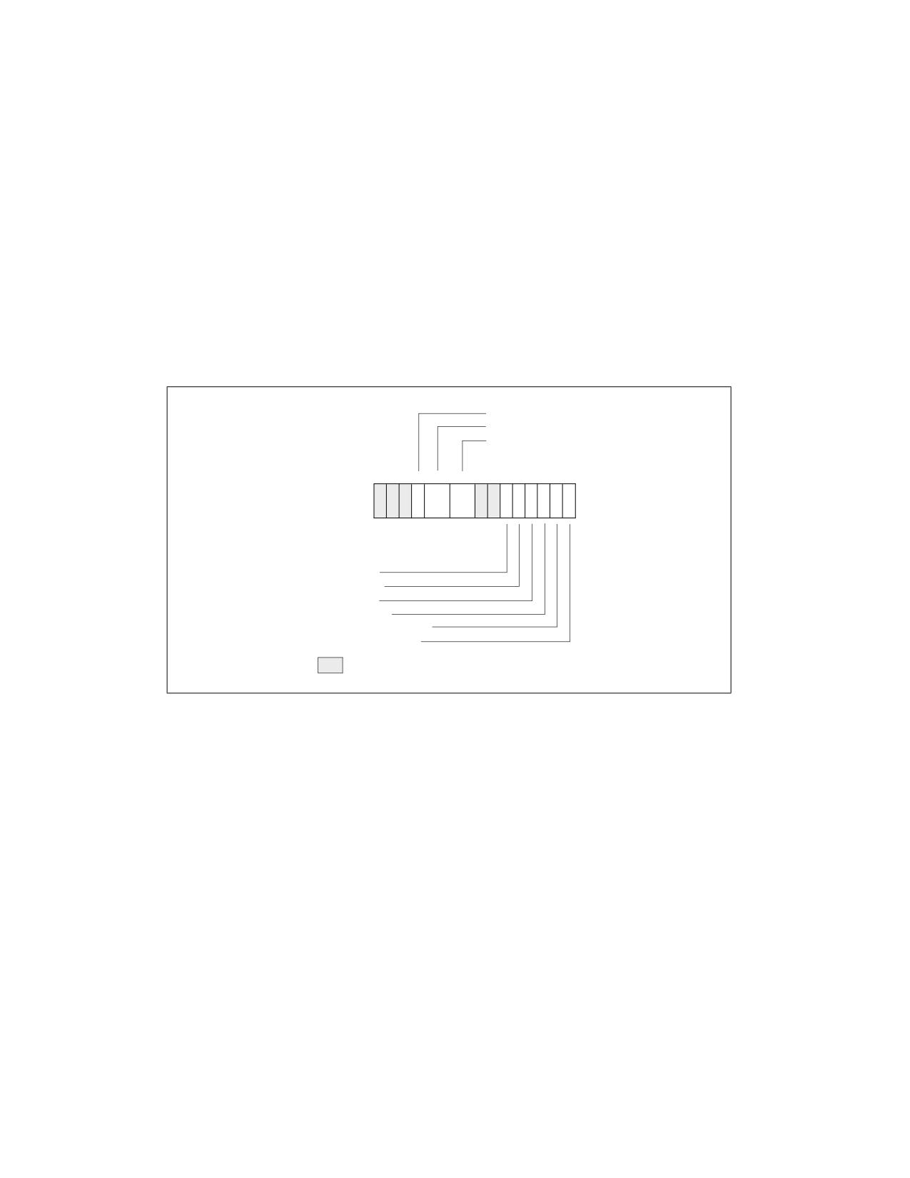
The 16-bit x87 FPU status register (see Figure 8-4) indicates the current state of the x87 FPU. The flags in the x87
FPU status register include the FPU busy flag, top-of-stack (TOP) pointer, condition code flags, exception summary
status flag, stack fault flag, and exception flags. The x87 FPU sets the flags in this register to show the results of
operations.
FPU Busy
Top of Stack Pointer
15 14 13
11 10 9
8
7
6
5
4
3
2
1
0
C
C
C
C
E
S
P
U
O
Z
D
I
B
TOP
3
2
1
0
S
F
E
E
E
E
E
E
Condition
Code
Exception Summary Status
Stack Fault
Exception Flags
Precision
Underflow
Overflow
Zero Divide
Denormalized Operand
Invalid Operation
Figure 8-4. x87 FPU Status Word
The contents of the x87 FPU status register (referred to as the x87 FPU status word) can be stored in memory using
the FSTSW/FNSTSW, FSTENV/FNSTENV, FSAVE/FNSAVE, and FXSAVE instructions. It can also be stored in the AX
register of the integer unit, using the FSTSW/FNSTSW instructions.
8.1.3.1
Top of Stack (TOP) Pointer
A pointer to the x87 FPU data register that is currently at the top of the x87 FPU register stack is contained in bits
11 through 13 of the x87 FPU status word. This pointer, which is commonly referred to as TOP (for top-of-stack),
is a binary value from 0 to 7. See Section 8.1.2, “x87 FPU Data Registers,” for more information about the TOP
pointer.
8.1.3.2
Condition Code Flags
The four condition code flags (C0 through C3) indicate the results of floating-point comparison and arithmetic oper-
ations. Table 8-1 summarizes the manner in which the floating-point instructions set the condition code flags.
These condition code bits are used principally for conditional branching and for storage of information used in
exception handling (see Section 8.1.4, “Branching and Conditional Moves on Condition Codes”).
As shown in Table 8-1, the C1 condition code flag is used for a variety of functions. When both the IE and SF flags
in the x87 FPU status word are set, indicating a stack overflow or underflow exception (#IS), the C1 flag distin-
guishes between overflow (C1 = 1) and underflow (C1 = 0). When the PE flag in the status word is set, indicating
an inexact (rounded) result, the C1 flag is set to 1 if the last rounding by the instruction was upward. The FXAM
instruction sets C1 to the sign of the value being examined.
8-4
Vol. 1

PROGRAMMING WITH THE X87 FPU
The C2 condition code flag is used by the FPREM and FPREM1 instructions to indicate an incomplete reduction (or
partial remainder). When a successful reduction has been completed, the C0, C3, and C1 condition code flags are
set to the three least-significant bits of the quotient (Q2, Q1, and Q0, respectively). See “FPREM1-Partial
Remainder” in Chapter 3, “Instruction Set Reference, A-L,” of the Intel® 64 and IA-32 Architectures Software
Developer’s Manual, Volume 2A, for more information on how these instructions use the condition code flags.
The FPTAN, FSIN, FCOS, and FSINCOS instructions set the C2 flag to 1 to indicate that the source operand is
beyond the allowable range of ±263 and clear the C2 flag if the source operand is within the allowable range.
Where the state of the condition code flags are listed as undefined in Table 8-1, do not rely on any specific value in
these flags.
8.1.3.3
x87 FPU Floating-Point Exception Flags
The six x87 FPU floating-point exception flags (bits 0 through 5) of the x87 FPU status word indicate that one or
more floating-point exceptions have been detected since the bits were last cleared. The individual exception flags
(IE, DE, ZE, OE, UE, and PE) are described in detail in Section 8.4, “x87 FPU Floating-Point Exception Handling.”
Each of the exception flags can be masked by an exception mask bit in the x87 FPU control word (see Section 8.1.5,
“x87 FPU Control Word”). The exception summary status flag (ES, bit 7) is set when any of the unmasked exception
flags are set. When the ES flag is set, the x87 FPU exception handler is invoked, using one of the techniques
described in Section 8.7, “Handling x87 FPU Exceptions in Software.” (Note that if an exception flag is masked, the
x87 FPU will still set the appropriate flag if the associated exception occurs, but it will not set the ES flag.)
The exception flags are “sticky” bits (once set, they remain set until explicitly cleared). They can be cleared by
executing the FCLEX/FNCLEX (clear exceptions) instructions, by reinitializing the x87 FPU with the FINIT/FNINIT or
FSAVE/FNSAVE instructions, or by overwriting the flags with an FRSTOR or FLDENV instruction.
The B-bit (bit 15) is included for 8087 compatibility only. It reflects the contents of the ES flag.
Table 8-1. Condition Code Interpretation
Instruction
C0
C3
C2
C1
FCOM, FCOMP, FCOMPP, FICOM, FICOMP, FTST,
Result of Comparison
Operands
0 or #IS
FUCOM, FUCOMP, FUCOMPP
are not
Comparable
FCOMI, FCOMIP, FUCOMI, FUCOMIP
Undefined. (These instructions set the
#IS
status flags in the EFLAGS register.)
FXAM
Operand class
Sign
FPREM, FPREM1
Q2
Q1
0 = reduction
Q0 or #IS
complete
1 = reduction
incomplete
F2XM1, FADD, FADDP, FBSTP, FCMOVcc,
Undefined
Roundup or #IS
FIADD, FDIV, FDIVP, FDIVR, FDIVRP, FIDIV,
FIDIVR, FIMUL, FIST, FISTP, FISUB, FISUBR,
FMUL, FMULP, FPATAN, FRNDINT, FSCALE, FST,
FSTP, FSUB, FSUBP, FSUBR, FSUBRP, FSQRT,
FYL2X, FYL2XP1
FCOS, FSIN, FSINCOS, FPTAN
Undefined
0 = source
Roundup or #IS
operand within
(Undefined if C2 =
range
1)
1 = source
operand out of
range
FABS, FBLD, FCHS, FDECSTP, FILD, FINCSTP,
Undefined
0 or #IS
FLD, Load Constants, FSTP (ext. prec.), FXCH,
FXTRACT
Vol. 1
8-5
PROGRAMMING WITH THE X87 FPU
Table 8-1. Condition Code Interpretation (Contd.)
FLDENV, FRSTOR
Each bit loaded from memory
FFREE, FLDCW, FCLEX/FNCLEX, FNOP,
FSTCW/FNSTCW, FSTENV/FNSTENV,
Undefined
FSTSW/FNSTSW,
FINIT/FNINIT, FSAVE/FNSAVE
0
0
0
0
8.1.3.4
Stack Fault Flag
The stack fault flag (bit 6 of the x87 FPU status word) indicates that stack overflow or stack underflow has occurred
with data in the x87 FPU data register stack. The x87 FPU explicitly sets the SF flag when it detects a stack overflow
or underflow condition, but it does not explicitly clear the flag when it detects an invalid-arithmetic-operand condi-
tion.
When this flag is set, the condition code flag C1 indicates the nature of the fault: overflow (C1 = 1) and under-
flow (C1 = 0). The SF flag is a “sticky” flag, meaning that after it is set, the processor does not clear it until it is
explicitly instructed to do so (for example, by an FINIT/FNINIT, FCLEX/FNCLEX, or FSAVE/FNSAVE instruction).
See Section 8.1.7, “x87 FPU Tag Word,” for more information on x87 FPU stack faults.
8.1.4
Branching and Conditional Moves on Condition Codes
The x87 FPU (beginning with the P6 family processors) supports two mechanisms for branching and performing
conditional moves according to comparisons of two floating-point values. These mechanism are referred to here as
the “old mechanism” and the “new mechanism.”
The old mechanism is available in the x87 FPU prior to the P6 family processors and in P6 family processors. This
mechanism uses the floating-point compare instructions (FCOM, FCOMP, FCOMPP, FTST, FUCOMPP, FICOM, and
FICOMP) to compare two floating-point values and set the condition code flags (C0 through C3) according to the
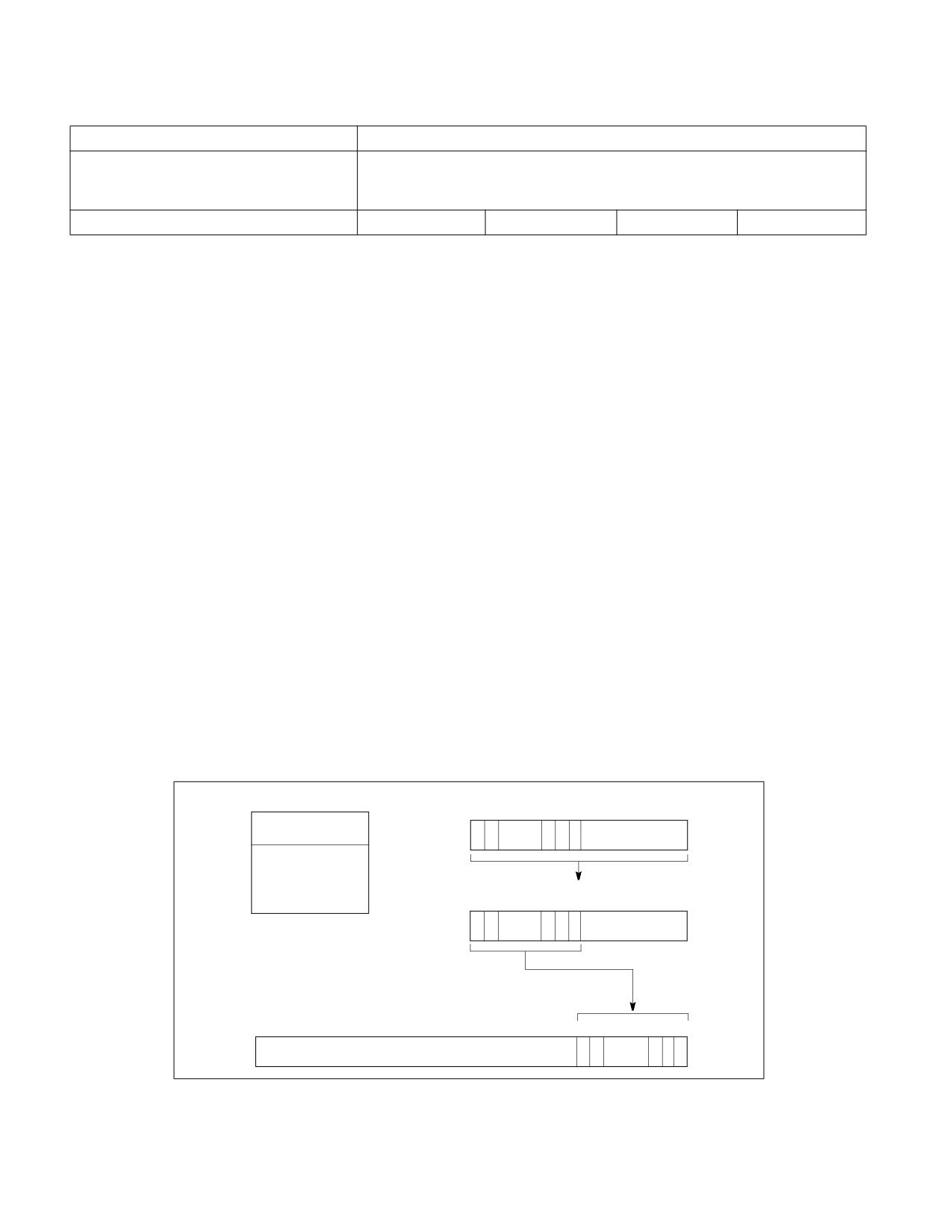
results. The contents of the condition code flags are then copied into the status flags of the EFLAGS register using
a two step process (see Figure 8-5):
1. The FSTSW AX instruction moves the x87 FPU status word into the AX register.
2. The SAHF instruction copies the upper 8 bits of the AX register, which includes the condition code flags, into the
lower 8 bits of the EFLAGS register.
When the condition code flags have been loaded into the EFLAGS register, conditional jumps or conditional moves
can be performed based on the new settings of the status flags in the EFLAGS register.
15
x87 FPU Status Word
0
Condition
Status
C
C
C
C
Code
Flag
3
2
1
0
C0
CF
C1
(none)
C2
PF
FSTSW AX Instruction
C3
ZF
15
AX Register
0
C
C
C
C
3
2
1
0
SAHF Instruction
31
EFLAGS Register
7
0
Z
P
C
1
F
F
F
Figure 8-5. Moving the Condition Codes to the EFLAGS Register
8-6
Vol. 1
PROGRAMMING WITH THE X87 FPU
The new mechanism is available beginning with the P6 family processors. Using this mechanism, the new floating-
point compare and set EFLAGS instructions (FCOMI, FCOMIP, FUCOMI, and FUCOMIP) compare two floating-point
values and set the ZF, PF, and CF flags in the EFLAGS register directly. A single instruction thus replaces the three
instructions required by the old mechanism.
Note also that the FCMOVcc instructions (also new in the P6 family processors) allow conditional moves of floating-
point values (values in the x87 FPU data registers) based on the setting of the status flags (ZF, PF, and CF) in the
EFLAGS register. These instructions eliminate the need for an IF statement to perform conditional moves of
floating-point values.
8.1.5
x87 FPU Control Word
The 16-bit x87 FPU control word (see Figure 8-6) controls the precision of the x87 FPU and rounding method used.
It also contains the x87 FPU floating-point exception mask bits. The control word is cached in the x87 FPU control
register. The contents of this register can be loaded with the FLDCW instruction and stored in memory with the
FSTCW/FNSTCW instructions.
Infinity Control
Rounding Control
Precision Control
15 14 13 12 11 10 9
8
7
6
5
4
3
2
1
0
P
U
O
Z
D
I
X
RC
PC
M
M
M
M
M
M
Exception Masks
Precision
Underflow
Overflow
Zero Divide
Denormal Operand
Invalid Operation
Reserved
Figure 8-6. x87 FPU Control Word
When the x87 FPU is initialized with either an FINIT/FNINIT or FSAVE/FNSAVE instruction, the x87 FPU control
word is set to 037FH, which masks all floating-point exceptions, sets rounding to nearest, and sets the x87 FPU
precision to 64 bits.
8.1.5.1
x87 FPU Floating-Point Exception Mask Bits
The exception-flag mask bits (bits 0 through 5 of the x87 FPU control word) mask the 6 floating-point exception
flags in the x87 FPU status word. When one of these mask bits is set, its corresponding x87 FPU floating-point
exception is blocked from being generated.
8.1.5.2
Precision Control Field
The precision-control (PC) field (bits 8 and 9 of the x87 FPU control word) determines the precision (64, 53, or 24
bits) of floating-point calculations made by the x87 FPU (see Table 8-2). The default precision is double extended
precision, which uses the full 64-bit significand available with the double extended precision floating-point format
of the x87 FPU data registers. This setting is best suited for most applications, because it allows applications to take
full advantage of the maximum precision available with the x87 FPU data registers.
Vol. 1
8-7

PROGRAMMING WITH THE X87 FPU
Table 8-2. Precision Control Field (PC)
Precision
PC Field
Single Precision (24 bits)
00B
Reserved
01B
Double Precision (53 bits)
10B
Double Extended Precision (64 bits)
11B
The double precision and single precision settings reduce the size of the significand to 53 bits and 24 bits, respec-
tively. These settings are provided to support IEEE Standard 754 and to provide compatibility with the specifica-
tions of certain existing programming languages. Using these settings nullifies the advantages of the double
extended precision floating-point format's 64-bit significand length. When reduced precision is specified, the
rounding of the significand value clears the unused bits on the right to zeros.
The precision-control bits only affect the results of the following floating-point instructions: FADD, FADDP, FIADD,
FSUB, FSUBP, FISUB, FSUBR, FSUBRP, FISUBR, FMUL, FMULP, FIMUL, FDIV, FDIVP, FIDIV, FDIVR, FDIVRP, FIDIVR,
and FSQRT.
8.1.5.3
Rounding Control Field
The rounding-control (RC) field of the x87 FPU control register (bits 10 and 11) controls how the results of x87 FPU
floating-point instructions are rounded. See Section 4.8.4, “Rounding,” for a discussion of rounding of floating-
point values; See Section 4.8.4.1, “Rounding Control (RC) Fields,” for the encodings of the RC field.
8.1.6
Infinity Control Flag
The infinity control flag (bit 12 of the x87 FPU control word) is provided for compatibility with the Intel 287 Math
Coprocessor; it is not meaningful for later version x87 FPU coprocessors or IA-32 processors. See Section 4.8.3.3,
“Signed Infinities,” for information on how the x87 FPUs handle infinity values.
8.1.7
x87 FPU Tag Word
The 16-bit tag word (see Figure 8-7) indicates the contents of each the 8 registers in the x87 FPU data-register
stack (one 2-bit tag per register). The tag codes indicate whether a register contains a valid number, zero, or a
special floating-point number (NaN, infinity, denormal, or unsupported format), or whether it is empty. The x87
FPU tag word is cached in the x87 FPU in the x87 FPU tag word register. When the x87 FPU is initialized with either
an FINIT/FNINIT or FSAVE/FNSAVE instruction, the x87 FPU tag word is set to FFFFH, which marks all the x87 FPU
data registers as empty.
15
0
TAG(7)
T
AG(6)
TAG(5)
TAG(4)
TAG(3)
TAG(2)
TAG(1)
TAG(0)
TAG Values
00 - Valid
01 - Zero
10 - Special: invalid (NaN, unsupported), infinity, or denormal
11 - Empty
Figure 8-7. x87 FPU Tag Word
Each tag in the x87 FPU tag word corresponds to a physical register (numbers 0 through 7). The current top-of-
stack (TOP) pointer stored in the x87 FPU status word can be used to associate tags with registers relative to ST(0).
8-8
Vol. 1
PROGRAMMING WITH THE X87 FPU
The x87 FPU uses the tag values to detect stack overflow and underflow conditions (see Section 8.5.1.1, “Stack
Overflow or Underflow Exception (#IS)”).
Application programs and exception handlers can use this tag information to check the contents of an x87 FPU data
register without performing complex decoding of the actual data in the register. To read the tag register, it must be
stored in memory using either the FSTENV/FNSTENV or FSAVE/FNSAVE instructions. The location of the tag word
in memory after being saved with one of these instructions is shown in Figures 8-9 through 8-12.
Software cannot directly load or modify the tags in the tag register. The FLDENV and FRSTOR instructions load an
image of the tag register into the x87 FPU; however, the x87 FPU uses those tag values only to determine if the
data registers are empty (11B) or non-empty (00B, 01B, or 10B).
If the tag register image indicates that a data register is empty, the tag in the tag register for that data register is
marked empty (11B); if the tag register image indicates that the data register is non-empty, the x87 FPU reads the
actual value in the data register and sets the tag for the register accordingly. This action prevents a program from
setting the values in the tag register to incorrectly represent the actual contents of non-empty data registers.
8.1.8
x87 FPU Instruction and Data (Operand) Pointers
The x87 FPU stores pointers to the instruction and data (operand) for the last non-control instruction executed.
These are the x87 FPU instruction pointer and x87 FPU data (operand) pointers; software can save these pointers
to provide state information for exception handlers. The pointers are illustrated in Figure 8-1 (the figure illustrates
the pointers as used outside 64-bit mode; see below).
Note that the value in the x87 FPU data pointer is always a pointer to a memory operand. If the last non-control
instruction that was executed did not have a memory operand, the value in the data pointer is undefined
(reserved). If CPUID.07H.00H:EBX[6] = 1, the data pointer is updated only for x87 non-control instructions that
incur unmasked x87 exceptions.
The contents of the x87 FPU instruction and data pointers remain unchanged when any of the following instructions
are executed: FCLEX/FNCLEX, FLDCW, FSTCW/FNSTCW, FSTSW/FNSTSW, FSTENV/FNSTENV, FLDENV, and
WAIT/FWAIT.
For all the x87 FPUs and Numeric Processor Extensions (NPXs) except the 8087, the x87 FPU instruction pointer
points to any prefixes that preceded the instruction. For the 8087, the x87 FPU instruction pointer points only to
the actual opcode.
The x87 FPU instruction and data pointers each consists of an offset and a segment selector:
• The x87 FPU Instruction Pointer Offset (FIP) comprises 64 bits on processors that support IA-32e mode; on
other processors, it offset comprises 32 bits.
• The x87 FPU Instruction Pointer Selector (FCS) comprises 16 bits.
• The x87 FPU Data Pointer Offset (FDP) comprises 64 bits on processors that support IA-32e mode; on other
processors, it offset comprises 32 bits.
• The x87 FPU Data Pointer Selector (FDS) comprises 16 bits.
The pointers are accessed by the FINIT/FNINIT, FLDENV, FRSTOR, FSAVE/FNSAVE, FSTENV/FNSTENV, FXRSTOR,
FXSAVE, XRSTOR, XSAVE, and XSAVEOPT instructions as follows:
• FINIT/FNINIT. Each instruction clears FIP, FCS, FDP, and FDS.
• FLDENV, FRSTOR. These instructions use the memory formats given in Figures 8-9 through 8-12:
- For each of FIP and FDP, each instruction loads the lower 32 bits from memory and clears the upper 32 bits.
- If CR0.PE = 1, each instruction loads FCS and FDS from memory; otherwise, it clears them.
• FSAVE/FNSAVE, FSTENV/FNSTENV. These instructions use the memory formats given in Figures 8-9 through
8-12.
- Each instruction saves the lower 32 bits of each FIP and FDP into memory. the upper 32 bits are not saved.
- If CR0.PE = 1, each instruction saves FCS and FDS into memory. If CPUID.07H.00H:EBX[13] = 1, the
processor deprecates FCS and FDS; it saves each as 0000H.
- After saving these data into memory, FSAVE/FNSAVE clears FIP, FCS, FDP, and FDS.
Vol. 1
8-9

PROGRAMMING WITH THE X87 FPU
• FXRSTOR, XRSTOR. These instructions load data from a memory image whose format depend on operating
mode and the REX prefix. The memory formats are given in Tables 3-45, 3-48, and 3-49 in Chapter 3,
“Instruction Set Reference, A-L,” of the Intel® 64 and IA-32 Architectures Software Developer’s Manual,
Volume 2A.
- Outside of 64-bit mode or if REX.W = 0, the instructions operate as follows:
• For each of FIP and FDP, each instruction loads the lower 32 bits from memory and clears the upper 32
bits.
• Each instruction loads FCS and FDS from memory.
- In 64-bit mode with REX.W = 1, the instructions operate as follows:
• Each instruction loads FIP and FDP from memory.
• Each instruction clears FCS and FDS.
• FXSAVE, XSAVE, and XSAVEOPT. These instructions store data into a memory image whose format depend on
operating mode and the REX prefix. The memory formats are given in Tables 3-45, 3-48, and 3-49 in Chapter
3, “Instruction Set Reference, A-L,” of the Intel® 64 and IA-32 Architectures Software Developer’s Manual,
Volume 2A.
- Outside of 64-bit mode or if REX.W = 0, the instructions operate as follows:
• Each instruction saves the lower 32 bits of each of FIP and FDP into memory. The upper 32 bits are not
saved.
• Each instruction saves FCS and FDS into memory. If CPUID.07H.00H:EBX[13] = 1, the processor
deprecates FCS and FDS; it saves each as 0000H.
- In 64-bit mode with REX.W = 1, each instruction saves FIP and FDP into memory. FCS and FDS are not
saved.
8.1.9
Last Instruction Opcode
The x87 FPU stores in the 11-bit x87 FPU opcode register (FOP) the opcode of the last x87 non-control instruction
executed that incurred an unmasked x87 exception. (This information provides state information for exception
handlers.) Only the first and second opcode bytes (after all prefixes) are stored in the x87 FPU opcode register.
Figure 8-8 shows the encoding of these two bytes. Since the upper 5 bits of the first opcode byte are the same for
all floating-point opcodes (11011B), only the lower 3 bits of this byte are stored in the opcode register.
8.1.9.1
Fopcode Compatibility Sub-mode
Some Pentium 4 and Intel Xeon processors provide program control over the value stored into FOP. Here, bit 2 of
the IA32_MISC_ENABLE MSR enables (set) or disables (clear) the fopcode compatibility mode.
If fopcode compatibility mode is enabled, FOP is defined as it had been in previous IA-32 implementations, as the
opcode of the last x87 non-control instruction executed (even if that instruction did not incur an unmasked x87
exception).
1st Instruction Byte
2nd Instruction Byte
7
2
0
7
0
10
8
7
0
x87 FPU Opcode Register
Figure 8-8. Contents of x87 FPU Opcode Registers
8-10
Vol. 1

PROGRAMMING WITH THE X87 FPU
The fopcode compatibility mode should be enabled only when x87 FPU floating-point exception handlers are
designed to use the fopcode to analyze program performance or restart a program after an exception has been
handled.
More recent Intel 64 processors do not support fopcode compatibility mode and do not allow software to set bit 2
of the IA32_MISC_ENABLE MSR.
8.1.10 Saving the x87 FPU State with FSTENV/FNSTENV and FSAVE/FNSAVE
The FSTENV/FNSTENV and FSAVE/FNSAVE instructions store x87 FPU state information in memory for use by
exception handlers and other system and application software. The FSTENV/FNSTENV instruction saves the
contents of the status, control, tag, x87 FPU instruction pointer, x87 FPU data pointer, and opcode registers. The
FSAVE/FNSAVE instruction stores that information plus the contents of the x87 FPU data registers. Note that the
FSAVE/FNSAVE instruction also initializes the x87 FPU to default values (just as the FINIT/FNINIT instruction does)
after it has saved the original state of the x87 FPU.
The manner in which this information is stored in memory depends on the operating mode of the processor
(protected mode or real-address mode) and on the operand-size attribute in effect (32-bit or 16-bit). See Figures
8-9 through 8-12. In virtual-8086 mode or SMM, the real-address mode formats shown in Figure 8-12 is used. See
Chapter 34, “System Management Mode,” of the Intel® 64 and IA-32 Architectures Software Developer’s Manual,
Volume 3C, for information on using the x87 FPU while in SMM.
The FLDENV and FRSTOR instructions allow x87 FPU state information to be loaded from memory into the x87 FPU.
Here, the FLDENV instruction loads only the status, control, tag, x87 FPU instruction pointer, x87 FPU data pointer,
and opcode registers, and the FRSTOR instruction loads all the x87 FPU registers, including the x87 FPU stack
registers.
32-Bit Protected Mode Format
31
16
15
0
Control Word
0
Status Word
4
Tag Word
8
FPU Instruction Pointer Offset (FIP)
12
0 0 0 0 0
Bits 10:0 of opcode
FPU Instruction Pointer Selector
16
FPU Data Pointer Offset (FDP)
20
FPU Data Pointer Selector (FDS)
24
For instructions that also store x87 FPU data registers, the eight
80-bit registers (R0-R7) follow the above structure in sequence.
Figure 8-9. Protected Mode x87 FPU State Image in Memory, 32-Bit Format
Vol. 1
8-11

PROGRAMMING WITH THE X87 FPU
32-Bit Real-Address Mode Format
31
16
15
0
Control Word
0
Status Word
4
Tag Word
8
FIP[15:0]
12
0 0 0 0
FIP[31:16]
FOP[10:0]
16
FDP[15:0]
20
0 0 0 0
FDP[31:16]
0 0 0 0 0 0 0 0 0 0 0 0
24
For instructions that also store x87 FPU data registers, the eight
80-bit registers (R0-R7) follow the above structure in sequence.
Figure 8-10. Real Mode x87 FPU State Image in Memory, 32-Bit Format
16-Bit Protected Mode Format
15
0
Control Word
0
Status Word
2
Tag Word
4
FIP
6
FCS
8
FDP
10
FDS
12
Figure 8-11. Protected Mode x87 FPU State Image in Memory, 16-Bit Format
16-Bit Real-Address Mode and
Virtual-8086 Mode Format
15
0
Control Word
0
Status Word
2
Tag Word
4
FIP[15:0]
6
FIP[19:16]
0
Bits 10:0 of opcode
8
FDP[15:0]
10
FDP[19:16]
0
0 0 0 0 0 0 0 0 0 0 0
12
Figure 8-12. Real Mode x87 FPU State Image in Memory, 16-Bit Format
8.1.11 Saving the x87 FPU State with FXSAVE
The FXSAVE and FXRSTOR instructions save and restore, respectively, the x87 FPU state along with the state of the
XMM registers and the MXCSR register. Using the FXSAVE instruction to save the x87 FPU state has two benefits:
(1) FXSAVE executes faster than FSAVE, and (2) FXSAVE saves the entire x87 FPU, MMX, and XMM state in one
operation. See Section 10.5, “FXSAVE and FXRSTOR Instructions,” for additional information about these instruc-
tions.
8-12
Vol. 1
PROGRAMMING WITH THE X87 FPU
8.2
X87 FPU DATA TYPES
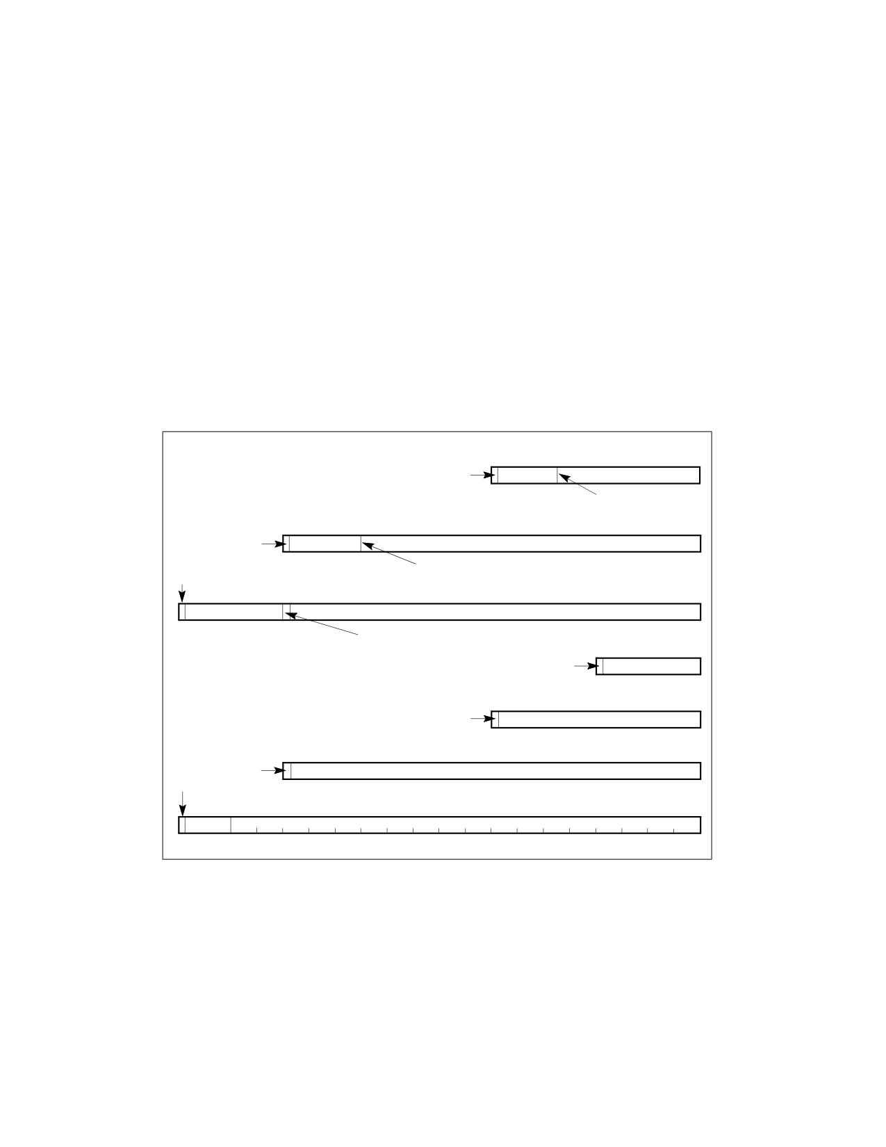
The x87 FPU recognizes and operates on the following seven data types (see Figures 8-13): single precision
floating-point, double precision floating-point, double extended precision floating-point, signed word integer,
signed doubleword integer, signed quadword integer, and packed BCD decimal integers.
For detailed information about these data types, see Section 4.2.2, “Floating-Point Data Types,” Section 4.2.1.2,
“Signed Integers,” and Section 4.7, “BCD and Packed BCD Integers.”
With the exception of the 80-bit double extended precision floating-point format, all of these data types exist in
memory only. When they are loaded into x87 FPU data registers, they are converted into double extended precision
floating-point format and operated on in that format.
Denormal values are also supported in each of the floating-point types, as required by IEEE Standard 754. When a
denormal number in single precision or double precision floating-point format is used as a source operand and the
denormal exception is masked, the x87 FPU automatically normalizes the number when it is converted to double
extended precision format.
When stored in memory, the least significant byte of an x87 FPU data-type value is stored at the initial address
specified for the value. Successive bytes from the value are then stored in successively higher addresses in
memory. The floating-point instructions load and store memory operands using only the initial address of the
operand.
Single Precision Floating-Point
Sign
Exp.
Fraction
3130
23 22
Implied Integer
0
Double Precision Floating-Point
Sign
Exponent
Fraction
6362
52 51
0
Implied Integer
Sign
Double Extended Precision Floating-Point
Exponent
Fraction
7978
646362
0
Integer
Word Integer
Sign
15
14
0
Doubleword Integer
Sign
3130
0
Quadword Integer
Sign
Sign
6362
0
Packed BCD Integers
X
D17 D16 D15 D14 D13 D12 D11 D10
D9
D8
D7
D6
D5
D4
D3
D2
D1
D0
79
78
7271
4 Bits = 1 BCD Digit
0
Figure 8-13. x87 FPU Data Type Formats
As a general rule, values should be stored in memory in double precision format. This format provides sufficient
range and precision to return correct results with a minimum of programmer attention. The single precision format
is useful for debugging algorithms, because rounding problems will manifest themselves more quickly in this
format. The double extended precision format is normally reserved for holding intermediate results in the x87 FPU
registers and constants. Its extra length is designed to shield final results from the effects of rounding and over-
flow/underflow in intermediate calculations. However, when an application requires the maximum range and preci-
sion of the x87 FPU (for data storage, computations, and results), values can be stored in memory in double
extended precision format.
Vol. 1
8-13

PROGRAMMING WITH THE X87 FPU
8.2.1
Indefinites
For each x87 FPU data type, one unique encoding is reserved for representing the special value indefinite. The x87
FPU produces indefinite values as responses to some masked floating-point invalid-operation exceptions. See
Tables 4-1, 4-3, and 4-5 for the encoding of the integer indefinite, QNaN floating-point indefinite, and packed BCD
integer indefinite, respectively.
The binary integer encoding 100..00B represents either of two things, depending on the circumstances of its use:
• The largest negative number supported by the format (-215, -231, or -263).
• The integer indefinite value.
If this encoding is used as a source operand (as in an integer load or integer arithmetic instruction), the x87 FPU
interprets it as the largest negative number representable in the format being used. If the x87 FPU detects an
invalid operation when storing an integer value in memory with an FIST/FISTP instruction and the invalid-operation
exception is masked, the x87 FPU stores the integer indefinite encoding in the destination operand as a masked
response to the exception. In situations where the origin of a value with this encoding may be ambiguous, the
invalid-operation exception flag can be examined to see if the value was produced as a response to an exception.
8.2.2
Unsupported Double Extended Precision Floating-Point Encodings and Pseudo-
Denormals
The double extended precision floating-point format permits many encodings that do not fall into any of the cate-
gories shown in Table 4-3. Table 8-3 shows these unsupported encodings. Some of these encodings were supported
by the Intel 287 math coprocessor; however, most of them are not supported by the Intel 387 math coprocessor
and later IA-32 processors. These encodings are no longer supported due to changes made in the final version of
IEEE Standard 754 that eliminated these encodings.
Specifically, the categories of encodings formerly known as pseudo-NaNs, pseudo-infinities, and un-normal
numbers are not supported and should not be used as operand values. The Intel 387 math coprocessor and later
IA-32 processors generate an invalid-operation exception when these encodings are encountered as operands.
Beginning with the Intel 387 math coprocessor, the encodings formerly known as pseudo-denormal numbers are
not generated by IA-32 processors. When encountered as operands, however, they are handled correctly, consid-
ering the biased exponent as 1 (and the unbiased exponent as -16382); that is, they are treated as denormals and
a denormal exception is generated. Pseudo-denormal numbers should not be used as operand values. They are
supported by current IA-32 processors (as described here) to support legacy code.
Table 8-3. Unsupported Double Extended Precision Floating-Point Encodings and Pseudo-Denormals
Significand
Class
Sign
Biased Exponent
Integer
Fraction
Positive
0
11..11
0
11..11
Pseudo-NaNs
Quiet
0
11..11
10..00
0
11..11
0
01..11
Signaling
0
11..11
00..01
Positive Floating-Point
Pseudo-infinity
0
11..11
0
00..00
0
11..10
0
11..11
Unnormals
0
00..01
00..00
Pseudo-denormals
0
00..00
1
11..11
0
00..00
00..00
8-14
Vol. 1

PROGRAMMING WITH THE X87 FPU
Table 8-3. Unsupported Double Extended Precision Floating-Point Encodings and Pseudo-Denormals (Contd.)
Negative Floating-Point
Pseudo-denormals
1
00..00
1
11..11
1
00..00
00..00
1
11..10
0
11..01
Unnormals
1
00..01
00..00
Pseudo-infinity
1
11..11
0
00..00
Negative Pseudo-NaNs
1
11..11
0
01..11
Signaling
1
11..11
00..01
1
11..11
0
11..11
Quiet
1
11..11
10..00
← 15 bits →
← 63 bits →
8.3
X87 FPU INSTRUCTION SET
The floating-point instructions that the x87 FPU supports can be grouped into six functional categories:
• Data transfer instructions.
• Basic arithmetic instructions.
• Comparison instructions.
• Transcendental instructions.
• Load constant instructions.
• x87 FPU control instructions.
See Section 5.2, “x87 FPU Instructions,” for a list of the floating-point instructions by category.
The following section briefly describes the instructions in each category. Detailed descriptions of the floating-point
instructions are given in the Intel® 64 and IA-32 Architectures Software Developer’s Manual, Volumes 2A, 2B, 2C,
& 2D.
8.3.1
Escape (ESC) Instructions
All of the instructions in the x87 FPU instruction set fall into a class of instructions known as escape (ESC) instruc-
tions. All of these instructions have a common opcode format, where the first byte of the opcode is one of the
numbers from D8H through DFH.
8.3.2
x87 FPU Instruction Operands
Most floating-point instructions require one or two operands, located on the x87 FPU data-register stack or in
memory. (None of the floating-point instructions accept immediate operands.)
When an operand is located in a data register, it is referenced relative to the ST(0) register (the register at the top
of the register stack), rather than by a physical register number. Often the ST(0) register is an implied operand.
Operands in memory can be referenced using the same operand addressing methods described in Section 3.7,
“Operand Addressing.”
8.3.3
Data Transfer Instructions
The data transfer instructions (see Table 8-4) perform the following operations:
Vol. 1
8-15

PROGRAMMING WITH THE X87 FPU
• Load a floating-point, integer, or packed BCD operand from memory into the ST(0) register.
• Store the value in an ST(0) register to memory in floating-point, integer, or packed BCD format.
• Move values between registers in the x87 FPU register stack.
The FLD (load floating-point) instruction pushes a floating-point operand from memory onto the top of the x87 FPU
data-register stack. If the operand is in single precision or double precision floating-point format, it is automatically
converted to double extended precision floating-point format. This instruction can also be used to push the value in
a selected x87 FPU data register onto the top of the register stack.
The FILD (load integer) instruction converts an integer operand in memory into double extended precision floating-
point format and pushes the value onto the top of the register stack. The FBLD (load packed decimal) instruction
performs the same load operation for a packed BCD operand in memory.
Table 8-4. Data Transfer Instructions
Floating-Point
Integer
Packed Decimal
FLD
Load Floating-Point
FILD
Load Integer
FBLD
Load Packed
Decimal
FST
Store Floating-Point
FIST
Store Integer
FSTP
Store Floating-Point and
FISTP
Store Integer
FBSTP
Store Packed
Pop
and Pop
Decimal and Pop
FXCH
Exchange Register
Contents
FCMOVcc
Conditional Move
The FST (store floating-point) and FIST (store integer) instructions store the value in register ST(0) in memory in
the destination format (floating-point or integer, respectively). Again, the format conversion is carried out auto-
matically.
The FSTP (store floating-point and pop), FISTP (store integer and pop), and FBSTP (store packed decimal and pop)
instructions store the value in the ST(0) registers into memory in the destination format (floating-point, integer, or
packed BCD), then performs a pop operation on the register stack. A pop operation causes the ST(0) register to be
marked empty and the stack pointer (TOP) in the x87 FPU control work to be incremented by 1. The FSTP instruc-
tion can also be used to copy the value in the ST(0) register to another x87 FPU register [ST(i)].
The FXCH (exchange register contents) instruction exchanges the value in a selected register in the stack [ST(i)]
with the value in ST(0).
The FCMOVcc (conditional move) instructions move the value in a selected register in the stack [ST(i)] to register
ST(0) if a condition specified with a condition code (cc) is satisfied (see Table 8-5). The condition being tested for
is represented by the status flags in the EFLAGS register. The condition code mnemonics are appended to the
letters “FCMOV” to form the mnemonic for a FCMOVcc instruction.
Table 8-5. Floating-Point Conditional Move Instructions
Instruction Mnemonic
Status Flag States
Condition Description
FCMOVB
CF=1
Below
FCMOVNB
CF=0
Not below
FCMOVE
ZF=1
Equal
FCMOVNE
ZF=0
Not equal
8-16
Vol. 1

PROGRAMMING WITH THE X87 FPU
Table 8-5. Floating-Point Conditional Move Instructions (Contd.)
Instruction Mnemonic
Status Flag States
Condition Description
FCMOVBE
CF=1 or ZF=1
Below or equal
FCMOVNBE
CF=0 or ZF=0
Not below nor equal
FCMOVU
PF=1
Unordered
FCMOVNU
PF=0
Not unordered
Like the CMOVcc instructions, the FCMOVcc instructions are useful for optimizing small IF constructions. They also
help eliminate branching overhead for IF operations and the possibility of branch mispredictions by the processor.
Software can check if the FCMOVcc instructions are supported by checking the processor’s feature information with
the CPUID instruction.
8.3.4
Load Constant Instructions
The following instructions push commonly used constants onto the top [ST(0)] of the x87 FPU register stack:
FLDZ
Load +0.0.
FLD1
Load +1.0.
FLDPI
Load π.
FLDL2T
Load log2 10.
FLDL2E
Load log2e.
FLDLG2
Load log102.
FLDLN2
Load loge2.
The constant values have full double extended precision floating-point precision (64 bits) and are accurate to
approximately 19 decimal digits. They are stored internally in a format more precise than double extended preci-
sion floating-point. When loading the constant, the x87 FPU rounds the more precise internal constant according
to the RC (rounding control) field of the x87 FPU control word. The inexact-result exception (#P) is not generated
as a result of this rounding, nor is the C1 flag set in the x87 FPU status word if the value is rounded up. See
Section 8.3.8, “Approximation of Pi,” for information on the π constant.
8.3.5
Basic Arithmetic Instructions
The following floating-point instructions perform basic arithmetic operations on floating-point numbers. Where
applicable, these instructions match IEEE Standard 754:
FADD/FADDP
Add floating-point.
FIADD
Add integer to floating-point.
FSUB/FSUBP
Subtract floating-point.
FISUB
Subtract integer from floating-point.
FSUBR/FSUBRP
Reverse subtract floating-point.
FISUBR
Reverse subtract floating-point from integer.
FMUL/FMULP
Multiply floating-point.
FIMUL
Multiply integer by floating-point.
FDIV/FDIVP
Divide floating-point.
FIDIV
Divide floating-point by integer.
FDIVR/FDIVRP
Reverse divide.
FIDIVR
Reverse divide integer by floating-point.
FABS
Absolute value.
FCHS
Change sign.
Vol. 1
8-17
PROGRAMMING WITH THE X87 FPU
FSQRT
Square root.
FPREM
Partial remainder.
FPREM1
IEEE partial remainder.
FRNDINT
Round to integral value.
FXTRACT
Extract exponent and significand.
The add, subtract, multiply, and divide instructions operate on the following types of operands:
• Two x87 FPU data registers.
• An x87 FPU data register and a floating-point or integer value in memory.
See Section 8.1.2, “x87 FPU Data Registers,” for a description of how operands are referenced on the data register
stack.
Operands in memory can be in single precision floating-point, double precision floating-point, word-integer, or
doubleword-integer format. They are converted to double extended precision floating-point format automatically.
Reverse versions of the subtract (FSUBR) and divide (FDIVR) instructions enable efficient coding. For example, the
following options are available with the FSUB and FSUBR instructions for operating on values in a specified x87 FPU
data register ST(i) and the ST(0) register:
FSUB:
ST(0) := ST(0) - ST(i)
ST(i) := ST(i) - ST(0)
FSUBR:
ST(0) := ST(i) - ST(0)
ST(i) := ST(0) - ST(i)
These instructions eliminate the need to exchange values between the ST(0) register and another x87 FPU register
to perform a subtraction or division.
The pop versions of the add, subtract, multiply, and divide instructions offer the option of popping the x87 FPU
register stack following the arithmetic operation. These instructions operate on values in the ST(i) and ST(0) regis-
ters, store the result in the ST(i) register, and pop the ST(0) register.
The FPREM instruction computes the remainder from the division of two operands in the manner used by the Intel
8087 and Intel 287 math coprocessors; the FPREM1 instruction computes the remainder in the manner specified in
IEEE Standard 754.
The FSQRT instruction computes the square root of the source operand.
The FRNDINT instruction returns a floating-point value that is the integral value closest to the source value in the
direction of the rounding mode specified in the RC field of the x87 FPU control word.
The FABS, FCHS, and FXTRACT instructions perform convenient arithmetic operations. The FABS instruction
produces the absolute value of the source operand. The FCHS instruction changes the sign of the source operand.
The FXTRACT instruction separates the source operand into its exponent and fraction and stores each value in a
register in floating-point format.
8.3.6
Comparison and Classification Instructions
The following instructions compare or classify floating-point values:
FCOM/FCOMP/FCOMPP
Compare floating-point and set x87 FPU condition code flags.
FUCOM/FUCOMP/FUCOMPP Unordered compare floating-point and set x87 FPU condition code flags.
FICOM/FICOMP
Compare integer and set x87 FPU condition code flags.
FCOMI/FCOMIP
Compare floating-point and set EFLAGS status flags.
FUCOMI/FUCOMIP
Unordered compare floating-point and set EFLAGS status flags.
FTST
Test (compare floating-point with 0.0).
8-18
Vol. 1

PROGRAMMING WITH THE X87 FPU
FXAM
Examine.
Comparison of floating-point values differ from comparison of integers because floating-point values have four
(rather than three) mutually exclusive relationships: less than, equal, greater than, and unordered.
The unordered relationship is true when at least one of the two values being compared is a NaN or in an unsup-
ported format. This additional relationship is required because, by definition, NaNs are not numbers, so they
cannot have less than, equal, or greater than relationships with other floating-point values.
The FCOM, FCOMP, and FCOMPP instructions compare the value in register ST(0) with a floating-point source
operand and set the condition code flags (C0, C2, and C3) in the x87 FPU status word according to the results (see
Table 8-6).
If an unordered condition is detected (one or both of the values are NaNs or in an undefined format), a floating-
point invalid-operation exception is generated.
The pop versions of the instruction pop the x87 FPU register stack once or twice after the comparison operation is
complete.
The FUCOM, FUCOMP, and FUCOMPP instructions operate the same as the FCOM, FCOMP, and FCOMPP instructions.
The only difference is that with the FUCOM, FUCOMP, and FUCOMPP instructions, if an unordered condition is
detected because one or both of the operands are QNaNs, the floating-point invalid-operation exception is not
generated.
Table 8-6. Setting of x87 FPU Condition Code Flags for Floating-Point Number Comparisons
Condition
C3
C2
C0
ST(0) > Source Operand
0
0
0
ST(0) < Source Operand
0
0
1
ST(0) = Source Operand
1
0
0
Unordered
1
1
1
The FICOM and FICOMP instructions also operate the same as the FCOM and FCOMP instructions, except that the
source operand is an integer value in memory. The integer value is automatically converted into an double
extended precision floating-point value prior to making the comparison. The FICOMP instruction pops the x87 FPU
register stack following the comparison operation.
The FTST instruction performs the same operation as the FCOM instruction, except that the value in register ST(0)
is always compared with the value 0.0.
The FCOMI and FCOMIP instructions were introduced into the IA-32 architecture in the P6 family processors. They
perform the same comparison as the FCOM and FCOMP instructions, except that they set the status flags (ZF, PF,
and CF) in the EFLAGS register to indicate the results of the comparison (see Table 8-7) instead of the x87 FPU
condition code flags. The FCOMI and FCOMIP instructions allow condition branch instructions (Jcc) to be executed
directly from the results of their comparison.
Table 8-7. Setting of EFLAGS Status Flags for Floating-Point Number Comparisons
Comparison Results
ZF
PF
CF
ST0 > ST(i)
0
0
0
ST0 < ST(i)
0
0
1
ST0 = ST(i)
1
0
0
Unordered
1
1
1
Software can check if the FCOMI and FCOMIP instructions are supported by checking the processor’s feature infor-
mation with the CPUID instruction.
The FUCOMI and FUCOMIP instructions operate the same as the FCOMI and FCOMIP instructions, except that they
do not generate a floating-point invalid-operation exception if the unordered condition is the result of one or both
of the operands being a QNaN. The FCOMIP and FUCOMIP instructions pop the x87 FPU register stack following the
comparison operation.
Vol. 1
8-19

PROGRAMMING WITH THE X87 FPU
The FXAM instruction determines the classification of the floating-point value in the ST(0) register (that is, whether
the value is zero, a denormal number, a normal finite number, ∞, a NaN, or an unsupported format) or that the
register is empty. It sets the x87 FPU condition code flags to indicate the classification (see “FXAM-Examine” in
Chapter 3, “Instruction Set Reference, A-L,” of the Intel® 64 and IA-32 Architectures Software Developer’s Manual,
Volume 2A). It also sets the C1 flag to indicate the sign of the value.
8.3.6.1
Branching on the x87 FPU Condition Codes
The processor does not offer any control-flow instructions that branch on the setting of the condition code flags
(C0, C2, and C3) in the x87 FPU status word. To branch on the state of these flags, the x87 FPU status word must
first be moved to the AX register in the integer unit. The FSTSW AX (store status word) instruction can be used for
this purpose. When these flags are in the AX register, the TEST instruction can be used to control conditional
branching as follows:
1. Check for an unordered result. Use the TEST instruction to compare the contents of the AX register with the
constant 0400H (see Table 8-8). This operation will clear the ZF flag in the EFLAGS register if the condition code
flags indicate an unordered result; otherwise, the ZF flag will be set. The JNZ instruction can then be used to
transfer control (if necessary) to a procedure for handling unordered operands.
Table 8-8. TEST Instruction Constants for Conditional Branching
Order
Constant
Branch
ST(0) > Source Operand
4500H
JZ
ST(0) < Source Operand
0100H
JNZ
ST(0) = Source Operand
4000H
JNZ
Unordered
0400H
JNZ
2. Check ordered comparison result. Use the constants given in Table 8-8 in the TEST instruction to test for a less
than, equal to, or greater than result, then use the corresponding conditional branch instruction to transfer
program control to the appropriate procedure or section of code.
If a program or procedure has been thoroughly tested and it incorporates periodic checks for QNaN results, then it
is not necessary to check for the unordered result every time a comparison is made.
See Section 8.1.4, “Branching and Conditional Moves on Condition Codes,” for another technique for branching on
x87 FPU condition codes.
Some non-comparison x87 FPU instructions update the condition code flags in the x87 FPU status word. To ensure
that the status word is not altered inadvertently, store it immediately following a comparison operation.
8.3.7
Trigonometric Instructions
The following instructions perform four common trigonometric functions:
FSIN
Sine.
FCOS
Cosine.
FSINCOS
Sine and cosine.
FPTAN
Tangent.
FPATAN
Arctangent.
These instructions operate on the top one or two registers of the x87 FPU register stack and they return their
results to the stack. The source operands for the FSIN, FCOS, FSINCOS, and FPTAN instructions must be given in
radians; the source operand for the FPATAN instruction is given in rectangular coordinate units.
The FSINCOS instruction returns both the sine and the cosine of a source operand value. It operates faster than
executing the FSIN and FCOS instructions in succession.
8-20
Vol. 1
PROGRAMMING WITH THE X87 FPU
The FPATAN instruction computes the arctangent of ST(1) divided by ST(0), returning a result in radians. It is
useful for converting rectangular coordinates to polar coordinates.
See Section 8.3.8, “Approximation of Pi,” and Section 8.3.10, “Transcendental Instruction Accuracy,” for informa-
tion regarding the accuracy of these instructions.
8.3.8
Approximation of Pi
When the argument (source operand) of a trigonometric function is within the domain of the function, the argu-
ment is automatically reduced by the appropriate multiple of 2π through the same reduction mechanism used by
the FPREM and FPREM1 instructions. The internal value of π (3.1415926…) that the x87 FPU uses for argument
reduction and other computations, denoted as Pi in the expression below. The numerical value of Pi can be written
as:
Pi = 0.f ∗ 22
where the fraction f is expressed in binary form as:
f = C90FDAA2 2168C234 C
(The spaces in the fraction above indicate 32-bit boundaries.)
The internal approximation Pi of the value π has a 66 significant bits. Since the exact value of π represented in
binary has the next 3 bits equal to 0, it means that Pi is the value of π rounded to nearest-even to 68 bits, and also
the value of π rounded toward zero (truncated) to 69 bits.
However, accuracy problems may arise because this relatively short finite approximation Pi of the number π is used
for calculating the reduced argument of the trigonometric function approximations in the implementations of FSIN,
FCOS, FSINCOS, and FPTAN. Alternately, this means that FSIN (x), FCOS (x), and FPTAN (x) are really approxi-
mating the mathematical functions sin (x * π /Pi), cos (x * π / Pi), and tan (x * π / Pi), and not exactly sin (x), cos
(x), and tan (x). (Note that FSINCOS is the equivalent of FSIN and FCOS combined together). The period of sin (x
* π /Pi) for example is 2* Pi, and not 2π.
See also Section 8.3.10, “Transcendental Instruction Accuracy,” for more information on the accuracy of these
functions.
8.3.9
Logarithmic, Exponential, and Scale
The following instructions provide two different logarithmic functions, an exponential function and a scale function:
FYL2X
Logarithm.
FYL2XP1
Logarithm epsilon.
F2XM1
Exponential.
FSCALE
Scale.
The FYL2X and FYL2XP1 instructions perform two different base 2 logarithmic operations. The FYL2X instruction
computes (y ∗ log2x). This operation permits the calculation of the log of any base using the following equation:
logb x = (1/log2 b) ∗ log2 x
The FYL2XP1 instruction computes (y ∗ log2(x + 1)). This operation provides optimum accuracy for values of x that
are close to 0.
The F2XM1 instruction computes (2x - 1). This instruction only operates on source values in the range -1.0 to +1.0.
The FSCALE instruction multiplies the source operand by a power of 2.
8.3.10 Transcendental Instruction Accuracy
New transcendental instruction algorithms were incorporated into the IA-32 architecture beginning with the
Pentium processors. These new algorithms (used in transcendental instructions FSIN, FCOS, FSINCOS, FPTAN,
FPATAN, F2XM1, FYL2X, and FYL2XP1) allow a higher level of accuracy than was possible in earlier IA-32 proces-
Vol. 1
8-21
PROGRAMMING WITH THE X87 FPU
sors and x87 math coprocessors. The accuracy of these instructions is measured in terms of units in the last
place (ulp). For a given argument x, let f(x) and F(x) be the correct and computed (approximate) function values,
respectively. The error in ulps is defined to be:
f(x) - F(x)
error
=
2k-63
where k is an integer such that:
-k
1
≤
2
f(x) < 2.
With the Pentium processor and later IA-32 processors, the worst case error on transcendental functions is less
than 1 ulp when rounding to the nearest (even) and less than 1.5 ulps when rounding in other modes. The func-
tions are guaranteed to be monotonic, with respect to the input operands, throughout the domain supported by the
instruction.
However, for FSIN, FCOS, FSINCOS, and FPTAN which approximate periodic trigonometric functions, the previous
statement about maximum ulp errors is true only when these instructions are applied to reduced argument (see
Section 8.3.8, “Approximation of Pi”). This is due to the fact that only 66 significant bits are retained in the finite
approximation Pi of the number π (3.1415926…), used internally for calculating the reduced argument in FSIN,
FCOS, FSINCOS, and FPTAN. This approximation of π is not always sufficiently accurate for good argument reduc-
tion.
For single precision, the argument of FSIN, FCOS, FSINCOS, and FPTAN must exceed 200,000 radians in order for
the error of the result to exceed 1 ulp when rounding to the nearest (even), or 1.5 ulps when rounding in other
(directed) rounding modes.
For double and double-extended precision, the ulp errors will grow above these thresholds for arguments much
smaller in magnitude. The ulp errors increase significantly when the argument approaches the value of π (or Pi) for
FSIN, and when it approaches π/2(or Pi/2) for FCOS, FSINCOS, and FPTAN.
For all three IEEE precisions supported (32-bit single precision, 64-bit double precision, and 80-bit double-
extended precision), applying FSIN, FCOS, FSINCOS, or FPTAN to arguments larger than a certain value can lead
to reduced arguments (calculated internally) that are inaccurate or even very inaccurate in some cases. This leads
to equally inaccurate approximations of the corresponding mathematical functions. In particular, arguments that
are close to certain values will lose significance when reduced, leading to increased relative (and ulp) errors in the
results of FSIN, FCOS, FSINCOS, and FPTAN. These values are:
• Any non-zero multiple of π for FSIN.
• Any multiple of π, plus π/2 for FCOS.
• Any non-zero multiple of π/2 for FSINCOS and FPTAN.
If the arguments passed to FSIN, FCOS, FSINCOS, and FPTAN are not close to these values then even the finite
approximation Pi of π used internally for argument reduction will allow for results that have good accuracy.
Therefore, in order to avoid such errors it is recommended to perform accurate argument reduction in software,
and to apply FSIN, FCOS, FSINCOS, and FPTAN to reduced arguments only. Regardless of the target precision
(single, double, or double-extended), it is safe to reduce the argument to a value smaller in absolute value than
about 3π/4 for FSIN, and smaller than about 3π/8 for FCOS, FSINCOS, and FPTAN.
The thresholds shown above are not exact. For example, accuracy measurements show that the double-extended
precision result of FSIN will not have errors larger than 0.72 ulp for |x| < 2.82 (so |x| < 3π/4 will ensure good accu-
racy, as 3π/4 < 2.82). On the same interval, double precision results from FSIN will have errors at most slightly
larger than 0.5 ulp, and single precision results will be correctly rounded in the vast majority of cases.
Likewise, the double-extended precision result of FCOS will not have errors larger than 0.82 ulp for |x| < 1.31 (so
|x| < 3π/8 will ensure good accuracy, as 3π/8 < 1.31). On the same interval, double precision results from FCOS
will have errors at most slightly larger than 0.5 ulp, and single precision results will be correctly rounded in the vast
majority of cases.
FSINCOS behaves similarly to FSIN and FCOS, combined as a pair.
8-22
Vol. 1
PROGRAMMING WITH THE X87 FPU
Finally, the double-extended precision result of FPTAN will not have errors larger than 0.78 ulp for |x| < 1.25 (so
|x| < 3π/8 will ensure good accuracy, as 3π/8 < 1.25). On the same interval, double precision results from FPTAN
will have errors at most slightly larger than 0.5 ulp, and single precision results will be correctly rounded in the vast
majority of cases.
A recommended alternative in order to avoid the accuracy issues that might be caused by FSIN, FCOS, FSINCOS,
and FPTAN, is to use good quality mathematical library implementations of the sin, cos, sincos, and tan functions,
for example those from the Intel® Math Library available in the Intel® Compiler.
The instructions FYL2X and FYL2XP1 are two operand instructions and are guaranteed to be within 1 ulp only when
y equals 1. When y is not equal to 1, the maximum ulp error is always within 1.35 ulps in round to nearest mode.
(For the two operand functions, monotonicity was proved by holding one of the operands constant.)
8.3.11 x87 FPU Control Instructions
The following instructions control the state and modes of operation of the x87 FPU. They also allow the status of the
x87 FPU to be examined:
FINIT/FNINIT
Initialize x87 FPU.
FLDCW
Load x87 FPU control word.
FSTCW/FNSTCW
Store x87 FPU control word.
FSTSW/FNSTSW
Store x87 FPU status word.
FCLEX/FNCLEX
Clear x87 FPU exception flags.
FLDENV
Load x87 FPU environment.
FSTENV/FNSTENV
Store x87 FPU environment.
FRSTOR
Restore x87 FPU state.
FSAVE/FNSAVE
Save x87 FPU state.
FINCSTP
Increment x87 FPU register stack pointer.
FDECSTP
Decrement x87 FPU register stack pointer.
FFREE
Free x87 FPU register.
FNOP
No operation.
WAIT/FWAIT
Check for and handle pending unmasked x87 FPU exceptions.
The FINIT/FNINIT instructions initialize the x87 FPU and its internal registers to default values.
The FLDCW instructions loads the x87 FPU control word register with a value from memory. The FSTCW/FNSTCW
and FSTSW/FNSTSW instructions store the x87 FPU control and status words, respectively, in memory (or for an
FSTSW/FNSTSW instruction in a general-purpose register).
The FSTENV/FNSTENV and FSAVE/FNSAVE instructions save the x87 FPU environment and state, respectively, in
memory. The x87 FPU environment includes all the x87 FPU’s control and status registers; the x87 FPU state
includes the x87 FPU environment and the data registers in the x87 FPU register stack. (The FSAVE/FNSAVE
instruction also initializes the x87 FPU to default values, like the FINIT/FNINIT instruction, after it saves the original
state of the x87 FPU.)
The FLDENV and FRSTOR instructions load the x87 FPU environment and state, respectively, from memory into the
x87 FPU. These instructions are commonly used when switching tasks or contexts.
The WAIT/FWAIT instructions are synchronization instructions. (They are actually mnemonics for the same
opcode.) These instructions check the x87 FPU status word for pending unmasked x87 FPU exceptions. If any
pending unmasked x87 FPU exceptions are found, they are handled before the processor resumes execution of the
instructions (integer, floating-point, or system instruction) in the instruction stream. The WAIT/FWAIT instructions
are provided to allow synchronization of instruction execution between the x87 FPU and the processor’s integer
unit. See Section 8.6, “x87 FPU Exception Synchronization,” for more information on the use of the WAIT/FWAIT
instructions.
Vol. 1
8-23
PROGRAMMING WITH THE X87 FPU
8.3.12 Waiting vs. Non-waiting Instructions
All of the x87 FPU instructions except a few special control instructions perform a wait operation (similar to the
WAIT/FWAIT instructions), to check for and handle pending unmasked x87 FPU floating-point exceptions, before
they perform their primary operation (such as adding two floating-point numbers). These instructions are called
waiting instructions. Some of the x87 FPU control instructions, such as FSTSW/FNSTSW, have both a waiting and
a non-waiting version. The waiting version (with the “F” prefix) executes a wait operation before it performs its
primary operation; whereas, the non-waiting version (with the “FN” prefix) ignores pending unmasked exceptions.
Non-waiting instructions allow software to save the current x87 FPU state without first handling pending exceptions
or to reset or reinitialize the x87 FPU without regard for pending exceptions.
NOTES
When operating a Pentium or Intel486 processor in MS-DOS compatibility mode, it is possible
(under unusual circumstances) for a non-waiting instruction to be interrupted prior to being
executed to handle a pending x87 FPU exception.
When operating a P6 family, Pentium 4, or Intel Xeon processor in MS-DOS compatibility mode,
non-waiting instructions cannot be interrupted in this way.
8.3.13 Unsupported x87 FPU Instructions
The Intel 8087 instructions FENI and FDISI and the Intel 287 math coprocessor instruction FSETPM perform no
function in the Intel 387 math coprocessor and later IA-32 processors. If these opcodes are detected in the instruc-
tion stream, the x87 FPU performs no specific operation and no internal x87 FPU states are affected.
8.4
X87 FPU FLOATING-POINT EXCEPTION HANDLING
The x87 FPU detects the six classes of exception conditions described in Section 4.9, “Overview of Floating-Point
Exceptions”:
• Invalid operation (#I), with two subclasses:
- Stack overflow or underflow (#IS).
- Invalid arithmetic operation (#IA).
• Denormalized operand (#D).
• Divide-by-zero (#Z).
• Numeric overflow (#O).
• Numeric underflow (#U).
• Inexact result (precision) (#P).
Each of the six exception classes has a corresponding flag bit in the x87 FPU status word and a mask bit in the x87
FPU control word (see Section 8.1.3, “x87 FPU Status Register,” and Section 8.1.5, “x87 FPU Control Word,” respec-
tively). In addition, the exception summary (ES) flag in the status word indicates when one or more unmasked
exceptions has been detected. The stack fault (SF) flag (also in the status word) distinguishes between the two
types of invalid-operation exceptions.
The mask bits can be set with FLDCW, FRSTOR, or FXRSTOR; they can be read with either FSTCW/FNSTCW,
FSAVE/FNSAVE, or FXSAVE. The flag bits can be read with the FSTSW/FNSTSW, FSAVE/FNSAVE, or FXSAVE
instruction.
NOTE
Section 4.9.1, “Floating-Point Exception Conditions,” provides a general overview of how the IA-32
processor detects and handles the various classes of floating-point exceptions. This information
pertains to the x87 FPU as well as the Intel SSE, SSE2, and SSE3 instructions.
8-24
Vol. 1

PROGRAMMING WITH THE X87 FPU
The following sections give specific information about how the x87 FPU handles floating-point exceptions that are
unique to the x87 FPU.
8.4.1
Arithmetic vs. Non-arithmetic Instructions
When dealing with floating-point exceptions, it is useful to distinguish between arithmetic instructions and non-
arithmetic instructions. Non-arithmetic instructions have no operands or do not make substantial changes to
their operands. Arithmetic instructions do make significant changes to their operands; in particular, they make
changes that could result in floating-point exceptions being signaled. Table 8-9 lists the non-arithmetic and arith-
metic instructions. It should be noted that some non-arithmetic instructions can signal a floating-point stack (fault)
exception, but this exception is not the result of an operation on an operand.
Table 8-9. Arithmetic and Non-arithmetic Instructions
Non-arithmetic Instructions
Arithmetic Instructions
FABS
F2XM1
FCHS
FADD/FADDP
FCLEX
FBLD
FDECSTP
FBSTP
FFREE
FCOM/FCOMP/FCOMPP
FINCSTP
FCOS
FINIT/FNINIT
FDIV/FDIVP/FDIVR/FDIVRP
FLD (register-to-register)
FIADD
FLD (extended format from memory)
FICOM/FICOMP
FLD constant
FIDIV/FIDIVR
FLDCW
FILD
FLDENV
FIMUL
FNOP
FIST/FISTP1
FRSTOR
FISUB/FISUBR
FSAVE/FNSAVE
FLD (single and double)
FST/FSTP (register-to-register)
FMUL/FMULP
FSTP (extended format to memory)
FPATAN
FSTCW/FNSTCW
FPREM/FPREM1
FSTENV/FNSTENV
FPTAN
FSTSW/FNSTSW
FRNDINT
WAIT/FWAIT
FSCALE
FXAM
FSIN
FXCH
FSINCOS
FSQRT
FST/FSTP (single and double)
FSUB/FSUBP/FSUBR/FSUBRP
FTST
FUCOM/FUCOMP/FUCOMPP
FXTRACT
FYL2X/FYL2XP1
Vol. 1
8-25

PROGRAMMING WITH THE X87 FPU
Table 8-9. Arithmetic and Non-arithmetic Instructions (Contd.)
Non-arithmetic Instructions
Arithmetic Instructions
NOTE:
1. The FISTTP instruction in SSE3 is an arithmetic x87 FPU instruction.
8.5
X87 FPU FLOATING-POINT EXCEPTION CONDITIONS
The following sections describe the various conditions that cause a floating-point exception to be generated by the
x87 FPU and the masked response of the x87 FPU when these conditions are detected. The Intel® 64 and IA-32
Architectures Software Developer’s Manual, Volumes 2A, 2B, 2C, & 2D, lists the floating-point exceptions that can
be signaled for each floating-point instruction.
See Section 4.9.2, “Floating-Point Exception Priority,” for a description of the rules for exception precedence when
more than one floating-point exception condition is detected for an instruction.
8.5.1
Invalid Operation Exception
The floating-point invalid-operation exception occurs in response to two sub-classes of operations:
• Stack overflow or underflow (#IS).
• Invalid arithmetic operand (#IA).
The flag for this exception (IE) is bit 0 of the x87 FPU status word, and the mask bit (IM) is bit 0 of the x87 FPU
control word. The stack fault flag (SF) of the x87 FPU status word indicates the type of operation that caused the
exception. When the SF flag is set to 1, a stack operation has resulted in stack overflow or underflow; when the flag
is cleared to 0, an arithmetic instruction has encountered an invalid operand. Note that the x87 FPU explicitly sets
the SF flag when it detects a stack overflow or underflow condition, but it does not explicitly clear the flag when it
detects an invalid-arithmetic-operand condition. As a result, the state of the SF flag can be 1 following an invalid-
arithmetic-operation exception, if it was not cleared from the last time a stack overflow or underflow condition
occurred. See Section 8.1.3.4, “Stack Fault Flag,” for more information about the SF flag.
8.5.1.1
Stack Overflow or Underflow Exception (#IS)
The x87 FPU tag word keeps track of the contents of the registers in the x87 FPU register stack (see Section 8.1.7,
“x87 FPU Tag Word”). It then uses this information to detect two different types of stack faults:
• Stack overflow - An instruction attempts to load a non-empty x87 FPU register from memory. A non-empty
register is defined as a register containing a zero (tag value of 01), a valid value (tag value of 00), or a special
value (tag value of 10).
• Stack underflow - An instruction references an empty x87 FPU register as a source operand, including
attempting to write the contents of an empty register to memory. An empty register has a tag value of 11.
NOTES
The term stack overflow originates from the situation where the program has loaded (pushed) eight
values from memory onto the x87 FPU register stack and the next value pushed on the stack causes
a stack wraparound to a register that already contains a value.
The term stack underflow originates from the opposite situation. Here, a program has stored
(popped) eight values from the x87 FPU register stack to memory and the next value popped from
the stack causes stack wraparound to an empty register.
When the x87 FPU detects stack overflow or underflow, it sets the IE flag (bit 0) and the SF flag (bit 6) in the x87
FPU status word to 1. It then sets condition-code flag C1 (bit 9) in the x87 FPU status word to 1 if stack overflow
occurred or to 0 if stack underflow occurred.
8-26
Vol. 1

PROGRAMMING WITH THE X87 FPU
If the invalid-operation exception is masked, the x87 FPU returns the floating-point, integer, or packed decimal
integer indefinite value to the destination operand, depending on the instruction being executed. This value over-
writes the destination register or memory location specified by the instruction.
If the invalid-operation exception is not masked, a software exception handler is invoked (see Section 8.7,
“Handling x87 FPU Exceptions in Software”) and the top-of-stack pointer (TOP) and source operands remain
unchanged.
8.5.1.2
Invalid Arithmetic Operand Exception (#IA)
The x87 FPU is able to detect a variety of invalid arithmetic operations that can be coded in a program. These oper-
ations are listed in Table 8-10. (This list includes the invalid operations defined in IEEE Standard 754.)
When the x87 FPU detects an invalid arithmetic operand, it sets the IE flag (bit 0) in the x87 FPU status word to 1.
If the invalid-operation exception is masked, the x87 FPU then returns an indefinite value or QNaN to the destina-
tion operand and/or sets the floating-point condition codes as shown in Table 8-10. If the invalid-operation excep-
tion is not masked, a software exception handler is invoked (see Section 8.7, “Handling x87 FPU Exceptions in
Software”) and the top-of-stack pointer (TOP) and source operands remain unchanged.
Table 8-10. Invalid Arithmetic Operations and the Masked Responses to Them
Condition
Masked Response
Any arithmetic operation on an operand that is in an unsupported
Return the QNaN floating-point indefinite value to the
format.
destination operand.
Any arithmetic operation on a SNaN.
Return a QNaN to the destination operand (see Table 4-8).
Ordered compare and test operations: one or both operands are
Set the condition code flags (C0, C2, and C3) in the x87 FPU
NaNs.
status word or the CF, PF, and ZF flags in the EFLAGS register to
111B (not comparable).
Addition: operands are opposite-signed infinities.
Return the QNaN floating-point indefinite value to the
Subtraction: operands are like-signed infinities.
destination operand.
Multiplication: ∞ by 0; 0 by ∞ .
Return the QNaN floating-point indefinite value to the
destination operand.
Division: ∞ by ∞ ; 0 by 0.
Return the QNaN floating-point indefinite value to the
destination operand.
Remainder instructions FPREM, FPREM1: modulus (divisor) is 0 or
Return the QNaN floating-point indefinite; clear condition code
dividend is ∞ .
flag C2 to 0.
Trigonometric instructions FCOS, FPTAN, FSIN, FSINCOS: source
Return the QNaN floating-point indefinite; clear condition code
operand is ∞ .
flag C2 to 0.
FSQRT: negative operand (except FSQRT (-0) = -0); FYL2X: negative
Return the QNaN floating-point indefinite value to the
operand (except FYL2X (-0) = -∞); FYL2XP1: operand more
destination operand.
negative than -1.
FBSTP: Converted value cannot be represented in 18 decimal digits,
Store packed BCD integer indefinite value in the destination
or source value is an SNaN, QNaN, ± ∞ , or in an unsupported
operand.
format.
FIST/FISTP: Converted value exceeds representable integer range
Store integer indefinite value in the destination operand.
of the destination operand, or source value is an SNaN, QNaN, ±∞,
or in an unsupported format.
FXCH: one or both registers are tagged empty.
Load empty registers with the QNaN floating-point indefinite
value, then perform the exchange.
Normally, when one or both of the source operands is a QNaN (and neither is an SNaN or in an unsupported
format), an invalid-operand exception is not generated. An exception to this rule is most of the compare instruc-
tions (such as the FCOM and FCOMI instructions) and the floating-point to integer conversion instructions
Vol. 1
8-27

PROGRAMMING WITH THE X87 FPU
(FIST/FISTP and FBSTP). With these instructions, a QNaN source operand will generate an invalid-operand excep-
tion.
8.5.2
Denormal Operand Exception (#D)
The x87 FPU signals the denormal-operand exception under the following conditions:
• If an arithmetic instruction attempts to operate on a denormal operand (see Section 4.8.3.2, “Normalized and
Denormalized Finite Numbers”).
• If an attempt is made to load a denormal single precision or double precision floating-point value into an x87
FPU register. (If the denormal value being loaded is a double extended precision floating-point value, the
denormal-operand exception is not reported.)
The flag (DE) for this exception is bit 1 of the x87 FPU status word, and the mask bit (DM) is bit 1 of the x87 FPU
control word.
When a denormal-operand exception occurs and the exception is masked, the x87 FPU sets the DE flag, then
proceeds with the instruction. The denormal operand in single- or double precision floating-point format is auto-
matically normalized when converted to the double extended precision floating-point format. Subsequent opera-
tions will benefit from the additional precision of the internal double extended precision floating-point format.
When a denormal-operand exception occurs and the exception is not masked, the DE flag is set and a software
exception handler is invoked (see Section 8.7, “Handling x87 FPU Exceptions in Software”). The top-of-stack
pointer (TOP) and source operands remain unchanged.
For additional information about the denormal-operation exception, see Section 4.9.1.2, “Denormal Operand
Exception (#D).”
8.5.3
Divide-By-Zero Exception (#Z)
The x87 FPU reports a floating-point divide-by-zero exception whenever an instruction attempts to divide a finite
non-zero operand by 0. The flag (ZE) for this exception is bit 2 of the x87 FPU status word, and the mask bit (ZM)
is bit 2 of the x87 FPU control word. The FDIV, FDIVP, FDIVR, FDIVRP, FIDIV, and FIDIVR instructions and the other
instructions that perform division internally (FYL2X and FXTRACT) can report the divide-by-zero exception.
When a divide-by-zero exception occurs and the exception is masked, the x87 FPU sets the ZE flag and returns the
values shown in Table 8-11. If the divide-by-zero exception is not masked, the ZE flag is set, a software exception
handler is invoked (see Section 8.7, “Handling x87 FPU Exceptions in Software”), and the top-of-stack pointer
(TOP) and source operands remain unchanged.
Table 8-11. Divide-By-Zero Conditions and the Masked Responses to Them
Condition
Masked Response
Divide or reverse divide operation with a
Returns an ∞ signed with the exclusive OR of the sign of the two operands to the
0 divisor.
destination operand.
FYL2X instruction.
Returns an ∞ signed with the opposite sign of the non-zero operand to the destination
operand.
FXTRACT instruction.
ST(1) is set to -∞; ST(0) is set to 0 with the same sign as the source operand.
8.5.4
Numeric Overflow Exception (#O)
The x87 FPU reports a floating-point numeric overflow exception (#O) whenever the rounded result of an arith-
metic instruction exceeds the largest allowable finite value that will fit into the floating-point format of the destina-
tion operand. (See Section 4.9.1.4, “Numeric Overflow Exception (#O),” for additional information about the
numeric overflow exception.)
When using the x87 FPU, numeric overflow can occur on arithmetic operations where the result is stored in an x87
FPU data register. It can also occur on store floating-point operations (using the FST and FSTP instructions), where
a within-range value in a data register is stored in memory in a single precision or double precision floating-point
8-28
Vol. 1
PROGRAMMING WITH THE X87 FPU
format. The numeric overflow exception cannot occur when storing values in an integer or BCD integer format.
Instead, the invalid-arithmetic-operand exception is signaled.
The flag (OE) for the numeric-overflow exception is bit 3 of the x87 FPU status word, and the mask bit (OM) is bit
3 of the x87 FPU control word.
When a numeric-overflow exception occurs and the exception is masked, the x87 FPU sets the OE flag and returns
one of the values shown in Table 4-11. The value returned depends on the current rounding mode of the x87 FPU
(see Section 8.1.5.3, “Rounding Control Field”).
The action that the x87 FPU takes when numeric overflow occurs and the numeric-overflow exception is not
masked, depends on whether the instruction is supposed to store the result in memory or on the register stack.
• Destination is a memory location - The OE flag is set and a software exception handler is invoked (see
Section 8.7, “Handling x87 FPU Exceptions in Software”). The top-of-stack pointer (TOP) and source and
destination operands remain unchanged. Because the data in the stack is in double extended precision format,
the exception handler has the option either of re-executing the store instruction after proper adjustment of the
operand or of rounding the significand on the stack to the destination's precision as the standard requires. The
exception handler should ultimately store a value into the destination location in memory if the program is to
continue.
• Destination is the register stack - The significand of the result is rounded according to current settings of
the precision and rounding control bits in the x87 FPU control word and the exponent of the result is adjusted
by dividing it by 224576. (For instructions not affected by the precision field, the significand is rounded to
double-extended precision.) The resulting value is stored in the destination operand. Condition code bit C1 in
the x87 FPU status word (called in this situation the “round-up bit”) is set if the significand was rounded upward
and cleared if the result was rounded toward 0. After the result is stored, the OE flag is set and a software
exception handler is invoked. The scaling bias value 24,576 is equal to 3 ∗ 213. Biasing the exponent by 24,576
normally translates the number as nearly as possible to the middle of the double extended precision floating-
point exponent range so that, if desired, it can be used in subsequent scaled operations with less risk of causing
further exceptions.
When using the FSCALE instruction, massive overflow can occur, where the result is too large to be repre-
sented, even with a bias-adjusted exponent. Here, if overflow occurs again, after the result has been biased, a
properly signed ∞ is stored in the destination operand.
8.5.5
Numeric Underflow Exception (#U)
The x87 FPU detects a potential floating-point numeric underflow condition whenever the result of an arithmetic
instruction is non-zero and tiny; that is, the magnitude of the rounded result with unbounded exponent is non-zero
and less than the smallest possible normalized, finite value that will fit into the floating-point format of the desti-
nation operand. See Section 4.9.1.5, “Numeric Underflow Exception (#U),” for additional information about the
numeric underflow exception.
Like numeric overflow, numeric underflow can occur on arithmetic operations where the result is stored in an x87
FPU data register. It can also occur on store floating-point operations (with the FST and FSTP instructions), where
a within-range value in a data register is stored in memory in the smaller single precision or double precision
floating-point formats. A numeric underflow exception cannot occur when storing values in an integer or BCD
integer format, because a value with magnitude less than 1 is always rounded to an integral value of 0 or 1,
depending on the rounding mode in effect.
The flag (UE) for the numeric-underflow exception is bit 4 of the x87 FPU status word, and the mask bit (UM) is bit
4 of the x87 FPU control word.
When a numeric-underflow condition occurs and the exception is masked, the x87 FPU performs the operation
described in Section 4.9.1.5, “Numeric Underflow Exception (#U).”
Vol. 1
8-29
PROGRAMMING WITH THE X87 FPU
When the exception is not masked, the action of the x87 FPU depends on whether the instruction is supposed to
store the result in a memory location or on the x87 FPU register stack.
• Destination is a memory location - (Can occur only with a store instruction.) The UE flag is set and a
software exception handler is invoked; see Section 8.2, “x87 FPU Data Types.” The top-of-stack pointer (TOP)
and source and destination operands remain unchanged, and no result is stored in memory.
Because the data in the stack is in double extended precision format, the exception handler has the option
either of re-executing the store instruction after proper adjustment of the operand or of rounding the
significand on the stack to the destination's precision as the standard requires. The exception handler should
ultimately store a value into the destination location in memory if the program is to continue.
• Destination is the register stack - The significand of the result is rounded according to current settings of
the precision and rounding control bits in the x87 FPU control word and the exponent of the result is adjusted
by multiplying it by 224576. (For instructions not affected by the precision field, the significand is rounded to
double extended precision.) The resulting value is stored in the destination operand. Condition code bit C1 in
the x87 FPU status register (acting here as a “round-up bit”) is set if the significand was rounded upward and
cleared if the result was rounded toward 0. After the result is stored, the UE flag is set and a software exception
handler is invoked. The scaling bias value 24,576 is the same as is used for the overflow exception and has the
same effect, which is to translate the result as nearly as possible to the middle of the double extended precision
floating-point exponent range.
When using the FSCALE instruction, massive underflow can occur, where the magnitude of the result is too
small to be represented, even with a bias-adjusted exponent. Here, if underflow occurs again after the result
has been biased, a properly signed 0 is stored in the destination operand.
8.5.6
Inexact-Result (Precision) Exception (#P)
The inexact-result exception (also called the precision exception) occurs if the result of an operation is not exactly
representable in the destination format. (See Section 4.9.1.6, “Inexact-Result (Precision) Exception (#P),” for
additional information about the numeric overflow exception.) Note that the transcendental instructions (FSIN,
FCOS, FSINCOS, FPTAN, FPATAN, F2XM1, FYL2X, and FYL2XP1) by nature produce inexact results.
The inexact-result exception flag (PE) is bit 5 of the x87 FPU status word, and the mask bit (PM) is bit 5 of the x87
FPU control word.
If the inexact-result exception is masked when an inexact-result condition occurs and a numeric overflow or under-
flow condition has not occurred, the x87 FPU handles the exception as described in Section 4.9.1.6, “Inexact-Result
(Precision) Exception (#P),” with one additional action. The C1 (round-up) bit in the x87 FPU status word is set to
indicate whether the inexact result was rounded up (C1 is set) or “not rounded up” (C1 is cleared). In the “not
rounded up” case, the least-significant bits of the inexact result are truncated so that the result fits in the destina-
tion format.
If the inexact-result exception is not masked when an inexact result occurs and numeric overflow or underflow has
not occurred, the x87 FPU handles the exception as described in the previous paragraph and, in addition, invokes
a software exception handler.
If an inexact result occurs in conjunction with numeric overflow or underflow, the x87 FPU carries out one of the
following operations:
• If an inexact result occurs in conjunction with masked overflow or underflow, the OE or UE flag and the PE flag
are set and the result is stored as described for the overflow or underflow exceptions (see Section 8.5.4,
“Numeric Overflow Exception (#O),” or Section 8.5.5, “Numeric Underflow Exception (#U)”). If the inexact
result exception is unmasked, the x87 FPU also invokes a software exception handler.
• If an inexact result occurs in conjunction with unmasked overflow or underflow and the destination operand is
a register, the OE or UE flag and the PE flag are set, the result is stored as described for the overflow or
underflow exceptions (see Section 8.5.4, “Numeric Overflow Exception (#O),” or Section 8.5.5, “Numeric
Underflow Exception (#U)”) and a software exception handler is invoked.
If an unmasked numeric overflow or underflow exception occurs and the destination operand is a memory location
(which can happen only for a floating-point store), the inexact-result condition is not reported and the C1 flag is
cleared.
8-30
Vol. 1
PROGRAMMING WITH THE X87 FPU
8.6
X87 FPU EXCEPTION SYNCHRONIZATION
Because the integer unit and x87 FPU are separate execution units, it is possible for the processor to execute
floating-point, integer, and system instructions concurrently. No special programming techniques are required to
gain the advantages of concurrent execution. (Floating-point instructions are placed in the instruction stream along
with the integer and system instructions.) However, concurrent execution can cause problems for floating-point
exception handlers.
This problem is related to the way the x87 FPU signals the existence of unmasked floating-point exceptions.
(Special exception synchronization is not required for masked floating-point exceptions, because the x87 FPU
always returns a masked result to the destination operand.)
When a floating-point exception is unmasked and the exception condition occurs, the x87 FPU stops further execu-
tion of the floating-point instruction and signals the exception event. On the next occurrence of a floating-point
instruction or a WAIT/FWAIT instruction in the instruction stream, the processor checks the ES flag in the x87 FPU
status word for pending floating-point exceptions. If floating-point exceptions are pending, the x87 FPU makes an
implicit call (traps) to the floating-point software exception handler. The exception handler can then execute
recovery procedures for selected or all floating-point exceptions.
Synchronization problems occur in the time between the moment when the exception is signaled and when it is
actually handled. Because of concurrent execution, integer or system instructions can be executed during this
time. It is thus possible for the source or destination operands for a floating-point instruction that faulted to be
overwritten in memory, making it impossible for the exception handler to analyze or recover from the exception.
To solve this problem, an exception synchronizing instruction (either a floating-point instruction or a WAIT/FWAIT
instruction) can be placed immediately after any floating-point instruction that might present a situation where
state information pertaining to a floating-point exception might be lost or corrupted. Floating-point instructions
that store data in memory are prime candidates for synchronization. For example, the following three lines of code
have the potential for exception synchronization problems:
FILD COUNT
;Floating-point instruction
INC COUNT
;Integer instruction
FSQRT
;Subsequent floating-point instruction
In this example, the INC instruction modifies the source operand of the floating-point instruction, FILD. If an
exception is signaled during the execution of the FILD instruction, the INC instruction would be allowed to over-
write the value stored in the COUNT memory location before the floating-point exception handler is called. With the
COUNT variable modified, the floating-point exception handler would not be able to recover from the error.
Rearranging the instructions, as follows, so that the FSQRT instruction follows the FILD instruction, synchronizes
floating-point exception handling and eliminates the possibility of the COUNT variable being overwritten before the
floating-point exception handler is invoked.
FILD COUNT
;Floating-point instruction
FSQRT
;Subsequent floating-point instruction synchronizes
;any exceptions generated by the FILD instruction.
INC COUNT
;Integer instruction
The FSQRT instruction does not require any synchronization, because the results of this instruction are stored in
the x87 FPU data registers and will remain there, undisturbed, until the next floating-point or WAIT/FWAIT instruc-
tion is executed. To absolutely ensure that any exceptions emanating from the FSQRT instruction are handled (for
example, prior to a procedure call), a WAIT instruction can be placed directly after the FSQRT instruction.
Note that some floating-point instructions (non-waiting instructions) do not check for pending unmasked excep-
tions (see Section 8.3.11, “x87 FPU Control Instructions”). They include the FNINIT, FNSTENV, FNSAVE, FNSTSW,
FNSTCW, and FNCLEX instructions. When an FNINIT, FNSTENV, FNSAVE, or FNCLEX instruction is executed, all
pending exceptions are essentially lost (either the x87 FPU status register is cleared or all exceptions are masked).
The FNSTSW and FNSTCW instructions do not check for pending interrupts, but they do not modify the x87 FPU
status and control registers. A subsequent “waiting” floating-point instruction can then handle any pending excep-
tions.
Vol. 1
8-31
PROGRAMMING WITH THE X87 FPU
8.7
HANDLING X87 FPU EXCEPTIONS IN SOFTWARE
The x87 FPU in Pentium and later IA-32 processors provides two different modes of operation for invoking a soft-
ware exception handler for floating-point exceptions: native mode and MS-DOS compatibility mode. The mode of
operation is selected by CR0.NE[bit 5]. See Chapter 2, “System Architecture Overview,” in the Intel® 64 and IA-32
Architectures Software Developer’s Manual, Volume 3A, for more information about the NE flag.
8.7.1
Native Mode
The native mode for handling floating-point exceptions is selected by setting CR0.NE[bit 5] to 1. In this mode, if the
x87 FPU detects an exception condition while executing a floating-point instruction and the exception is unmasked
(the mask bit for the exception is cleared), the x87 FPU sets the flag for the exception and the ES flag in the x87
FPU status word. It then invokes the software exception handler through the floating-point-error exception (#MF,
exception vector 16), immediately before execution of any of the following instructions in the processor’s instruc-
tion stream:
• The next floating-point instruction, unless it is one of the non-waiting instructions (FNINIT, FNCLEX, FNSTSW,
FNSTCW, FNSTENV, and FNSAVE).
• The next WAIT/FWAIT instruction.
• The next MMX instruction.
If the next floating-point instruction in the instruction stream is a non-waiting instruction, the x87 FPU executes the
instruction without invoking the software exception handler.
8.7.2
MS-DOS* Compatibility Sub-mode
If CR0.NE[bit 5] is 0, the MS-DOS compatibility mode for handling floating-point exceptions is selected. In this
mode, the software exception handler for floating-point exceptions is invoked externally using the processor’s
FERR#, INTR, and IGNNE# pins. This method of reporting floating-point errors and invoking an exception handler
is provided to support the floating-point exception handling mechanism used in PC systems that are running the
MS-DOS or Windows* 95 operating system.
Using FERR# and IGNNE# to handle floating-point exception is deprecated by modern operating systems, this
approach also limits newer processors to operate with one logical processor active.
The MS-DOS compatibility mode is typically used as follows to invoke the floating-point exception handler:
1. If the x87 FPU detects an unmasked floating-point exception, it sets the flag for the exception and the ES flag
in the x87 FPU status word.
2. If the IGNNE# pin is deasserted, the x87 FPU then asserts the FERR# pin either immediately, or else delayed
(deferred) until just before the execution of the next waiting floating-point instruction or MMX instruction.
Whether the FERR# pin is asserted immediately or delayed depends on the type of processor, the instruction,
and the type of exception.
3. If a preceding floating-point instruction has set the exception flag for an unmasked x87 FPU exception, the
processor freezes just before executing the next WAIT instruction, waiting floating-point instruction, or MMX
instruction. Whether the FERR# pin was asserted at the preceding floating-point instruction or is just now being
asserted, the freezing of the processor assures that the x87 FPU exception handler will be invoked before the
new floating-point (or MMX) instruction gets executed.
4. The FERR# pin is connected through external hardware to IRQ13 of a cascaded, programmable interrupt
controller (PIC). When the FERR# pin is asserted, the PIC is programmed to generate an interrupt 75H.
5. The PIC asserts the INTR pin on the processor to signal the interrupt 75H.
6. The BIOS for the PC system handles the interrupt 75H by branching to the interrupt 02H (NMI) interrupt
handler.
7. The interrupt 02H handler determines if the interrupt is the result of an NMI interrupt or a floating-point
exception.
8-32
Vol. 1
PROGRAMMING WITH THE X87 FPU
8. If a floating-point exception is detected, the interrupt 02H handler branches to the floating-point exception
handler.
If the IGNNE# pin is asserted, the processor ignores floating-point error conditions. This pin is provided to inhibit
floating-point exceptions from being generated while the floating-point exception handler is servicing a previously
signaled floating-point exception.
Appendix D, “Guidelines for Writing SIMD Floating-Point Exception Handlers,” describes the MS-DOS compatibility
mode in much greater detail. This mode is somewhat more complicated in the Intel486 and Pentium processor
implementations, as described in Appendix D.
8.7.3
Handling x87 FPU Exceptions in Software
Section 4.9.3, “Typical Actions of a Floating-Point Exception Handler,” shows actions that may be carried out by a
floating-point exception handler. The state of the x87 FPU can be saved with the FSTENV/FNSTENV or
FSAVE/FNSAVE instructions; see Section 8.1.10, “Saving the x87 FPU State with FSTENV/FNSTENV and
FSAVE/FNSAVE.”
If the faulting floating-point instruction is followed by one or more non-floating-point instructions, it may not be
useful to re-execute the faulting instruction. See Section 8.6, “x87 FPU Exception Synchronization,” for more infor-
mation on synchronizing floating-point exceptions.
In cases where the handler needs to restart program execution with the faulting instruction, the IRET instruction
cannot be used directly. The reason for this is that because the exception is not generated until the next floating-
point or WAIT/FWAIT instruction following the faulting floating-point instruction, the return instruction pointer on
the stack may not point to the faulting instruction. To restart program execution at the faulting instruction, the
exception handler must obtain a pointer to the instruction from the saved x87 FPU state information, load it into
the return instruction pointer location on the stack, and then execute the IRET instruction.
Vol. 1
8-33
PROGRAMMING WITH THE X87 FPU
8-34
Vol. 1
CHAPTER 9
PROGRAMMING WITH INTEL® MMX™ TECHNOLOGY
The Intel MMX technology was introduced into the IA-32 architecture in the Pentium II processor family and
Pentium processor with MMX technology. The extensions introduced in MMX technology support a single-instruc-
tion, multiple-data (SIMD) execution model that is designed to accelerate the performance of advanced media and
communications applications.
This chapter describes MMX technology.
9.1
OVERVIEW OF MMX TECHNOLOGY
MMX technology defines a simple and flexible SIMD execution model to handle 64-bit packed integer data. This
model adds the following features to the IA-32 architecture, while maintaining backwards compatibility with all IA-
32 applications and operating-system code:
• Eight new 64-bit data registers, called MMX registers.
• Three new packed data types:
- 64-bit packed byte integers (signed and unsigned).
- 64-bit packed word integers (signed and unsigned).
- 64-bit packed doubleword integers (signed and unsigned).
• Instructions that support the new data types and to handle MMX state management.
• Extensions to the CPUID instruction.
MMX technology is accessible from all the IA32-architecture execution modes (protected mode, real address mode,
and virtual 8086 mode). It does not add any new modes to the architecture.
The following sections of this chapter describe MMX technology’s programming environment, including MMX
register set, data types, and instruction set. Additional instructions that operate on MMX registers have been added
to the IA-32 architecture by the SSE/SSE2 extensions.
For more information, see:
• Section 10.4.4, “Intel® SSE 64-Bit SIMD Integer Instructions,” describes MMX instructions added to the IA-32
architecture with the SSE extensions.
• Section 11.4.2, “Intel® SSE2 64-Bit and 128-Bit SIMD Integer Instructions,” describes MMX instructions added
to the IA-32 architecture with SSE2 extensions.
• The Intel® 64 and IA-32 Architectures Software Developer’s Manual, Volumes 2A, 2B, 2C, & 2D, gives detailed
descriptions of MMX instructions.
• Chapter 15, “Intel® MMX™ Technology System Programming,” in the Intel® 64 and IA-32 Architectures
Software Developer’s Manual, Volume 3B, describes the manner in which MMX technology is integrated into the
IA-32 system programming model.
9.2
THE MMX TECHNOLOGY PROGRAMMING ENVIRONMENT
Figure 9-1 shows the execution environment for MMX technology. All MMX instructions operate on MMX registers,
the general-purpose registers, and/or memory as follows:
• MMX registers - These eight registers (see Figure 9-1) are used to perform operations on 64-bit packed
integer data. They are named MM0 through MM7.
Vol. 1
9-1

PROGRAMMING WITH INTEL® MMX™ TECHNOLOGY
Address Space
232 -1
MMX Registers
Eight 64-Bit
General-Purpose
Registers
Eight 32-Bit
0
Figure 9-1. MMX Technology Execution Environment
• General-purpose registers - The eight general-purpose registers (see Figure 3-5) are used with existing IA-
32 addressing modes to address operands in memory. (MMX registers cannot be used to address memory).
General-purpose registers are also used to hold operands for some MMX technology operations. They are EAX,
EBX, ECX, EDX, EBP, ESI, EDI, and ESP.
9.2.1
MMX Technology in 64-Bit Mode and Compatibility Mode
In compatibility mode and 64-bit mode, MMX instructions function like they do in protected mode. Memory oper-
ands are specified using the ModR/M, SIB encoding described in Section 3.7.5.
9.2.2
MMX Registers
The MMX register set consists of eight 64-bit registers (see Figure 9-2), that are used to perform calculations on
the MMX packed integer data types. Values in MMX registers have the same format as a 64-bit quantity in memory.
The MMX registers have two data access modes: 64-bit access mode and 32-bit access mode. The 64-bit access
mode is used for:
•
64-bit memory accesses.
•
64-bit transfers between MMX registers.
• All pack, logical, and arithmetic instructions.
• Some unpack instructions.
The 32-bit access mode is used for:
•
32-bit memory accesses.
•
32-bit transfer between general-purpose registers and MMX registers.
• Some unpack instructions.
9-2
Vol. 1

PROGRAMMING WITH INTEL® MMX™ TECHNOLOGY
63
0
MM7
MM6
MM5
MM4
MM3
MM2
MM1
MM0
Figure 9-2. MMX Register Set
Although MMX registers are defined in the IA-32 architecture as separate registers, they are aliased to the registers
in the FPU data register stack (R0 through R7).
See also Section 9.5, “Compatibility with x87 FPU Architecture.”
9.2.3
MMX Data Types
MMX technology introduced the following 64-bit data types to the IA-32 architecture (see Figure 9-3):
•
64-bit packed byte integers - eight packed bytes.
•
64-bit packed word integers - four packed words.
•
64-bit packed doubleword integers - two packed doublewords.
MMX instructions move 64-bit packed data types (packed bytes, packed words, or packed doublewords) and the
quadword data type between MMX registers and memory or between MMX registers in 64-bit blocks. However,
when performing arithmetic or logical operations on the packed data types, MMX instructions operate in parallel on
the individual bytes, words, or doublewords contained in MMX registers; see Section 9.2.5, “Single Instruction,
Multiple Data (SIMD) Execution Model.”
Packed Byte Integers
63
0
Packed Word Integers
63
0
Packed Doubleword Integers
63
0
Figure 9-3. Data Types Introduced with the MMX Technology
9.2.4
Memory Data Formats
When stored in memory: bytes, words, and doublewords in the packed data types are stored in consecutive
addresses. The least significant byte, word, or doubleword is stored at the lowest address and the most significant
byte, word, or doubleword is stored at the high address. The ordering of bytes, words, or doublewords in memory
is always little endian. That is, the bytes with the low addresses are less significant than the bytes with high
addresses.
Vol. 1
9-3
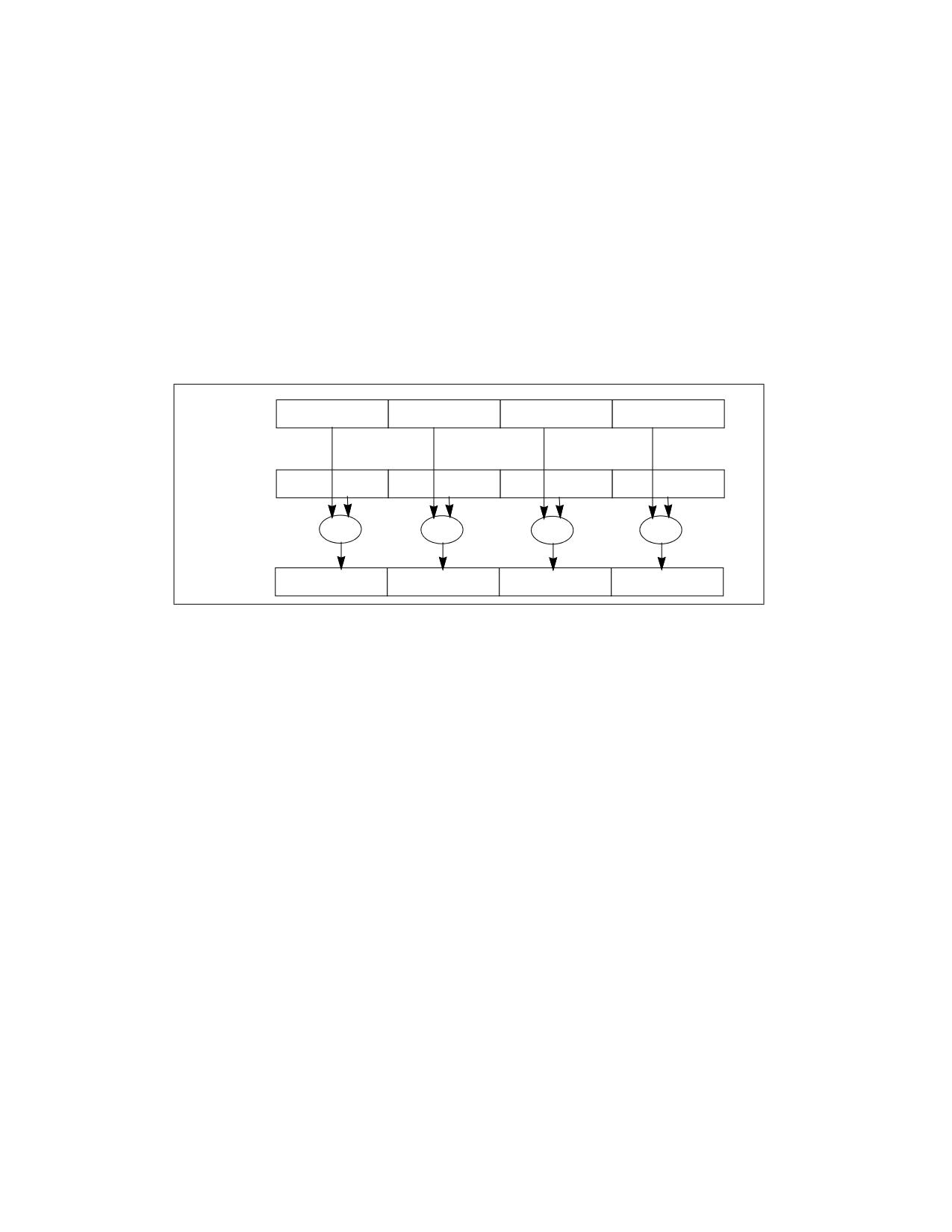
PROGRAMMING WITH INTEL® MMX™ TECHNOLOGY
9.2.5
Single Instruction, Multiple Data (SIMD) Execution Model
MMX technology uses the single instruction, multiple data (SIMD) technique for performing arithmetic and logical
operations on bytes, words, or doublewords packed into MMX registers (see Figure 9-4). For example, the PADDSW
instruction adds 4 signed word integers from one source operand to 4 signed word integers in a second source
operand and stores 4 word integer results in a destination operand. This SIMD technique speeds up software
performance by allowing the same operation to be carried out on multiple data elements in parallel. MMX tech-
nology supports parallel operations on byte, word, and doubleword data elements when contained in MMX regis-
ters.
The SIMD execution model supported in the MMX technology directly addresses the needs of modern media,
communications, and graphics applications, which often use sophisticated algorithms that perform the same oper-
ations on a large number of small data types (bytes, words, and doublewords). For example, most audio data is
represented in 16-bit (word) quantities. The MMX instructions can operate on 4 words simultaneously with one
instruction. Video and graphics information is commonly represented as palletized 8-bit (byte) quantities. In
Figure 9-4, one MMX instruction operates on 8 bytes simultaneously.
Source 1
X3
X2
X1
X0
Source 2
Y3
Y2
Y1
Y0
OP
OP
OP
OP
Destination
X3 OP Y3
X2 OP Y2
X1 OP Y1
X0 OP Y0
Figure 9-4. SIMD Execution Model
9.3
SATURATION AND WRAPAROUND MODES
When performing integer arithmetic, an operation may result in an out-of-range condition, where the true result
cannot be represented in the destination format. For example, when performing arithmetic on signed word inte-
gers, positive overflow can occur when the true signed result is larger than 16 bits.
The MMX technology provides three ways of handling out-of-range conditions:
• Wraparound arithmetic - With wraparound arithmetic, a true out-of-range result is truncated (that is, the
carry or overflow bit is ignored and only the least significant bits of the result are returned to the destination).
Wraparound arithmetic is suitable for applications that control the range of operands to prevent out-of-range
results. If the range of operands is not controlled, however, wraparound arithmetic can lead to large errors. For
example, adding two large signed numbers can cause positive overflow and produce a negative result.
• Signed saturation arithmetic - With signed saturation arithmetic, out-of-range results are limited to the
representable range of signed integers for the integer size being operated on (see Table 9-1). For example, if
positive overflow occurs when operating on signed word integers, the result is “saturated” to 7FFFH, which is
the largest positive integer that can be represented in 16 bits; if negative overflow occurs, the result is
saturated to 8000H.
• Unsigned saturation arithmetic - With unsigned saturation arithmetic, out-of-range results are limited to
the representable range of unsigned integers for the integer size. So, positive overflow when operating on
unsigned byte integers results in FFH being returned and negative overflow results in 00H being returned.
9-4
Vol. 1

PROGRAMMING WITH INTEL® MMX™ TECHNOLOGY
Table 9-1. Data Range Limits for Saturation
Data Type
Lower Limit
Upper Limit
Hexadecimal
Decimal
Hexadecimal
Decimal
Signed Byte
80H
-128
7FH
127
Signed Word
8000H
-32,768
7FFFH
32,767
Unsigned Byte
00H
0
FFH
255
Unsigned Word
0000H
0
FFFFH
65,535
Saturation arithmetic provides an answer for many overflow situations. For example, in color calculations, satura-
tion causes a color to remain pure black or pure white without allowing inversion. It also prevents wraparound arti-
facts from entering into computations when range checking of source operands it not used.
MMX instructions do not indicate overflow or underflow occurrence by generating exceptions or setting flags in the
EFLAGS register.
9.4
MMX INSTRUCTIONS
The MMX instruction set consists of 47 instructions, grouped into the following categories:
• Data transfer
• Arithmetic
• Comparison
• Conversion
• Unpacking
• Logical
• Shift
• Empty MMX state instruction (EMMS)
Table 9-2 gives a summary of the instructions in the MMX instruction set. The following sections give a brief over-
view of the instructions within each group.
NOTES
The MMX instructions described in this chapter are those instructions that are available in an IA-32
processor when CPUID.01H:EDX.MMX[23] = 1.
Section 10.4.4, “Intel® SSE 64-Bit SIMD Integer Instructions,” and Section 11.4.2, “Intel® SSE2
64-Bit and 128-Bit SIMD Integer Instructions,” list additional instructions included with the Intel
SSE/SSE2 extensions that operate on MMX registers but are not considered part of the MMX
instruction set.
Vol. 1
9-5

PROGRAMMING WITH INTEL® MMX™ TECHNOLOGY
Table 9-2. MMX Instruction Set Summary
Category
Wraparound
Signed Saturation
Unsigned Saturation
Arithmetic
Addition
PADDB, PADDW, PADDD
PADDSB, PADDSW
PADDUSB, PADDUSW
PSUBB, PSUBW, PSUBD
PSUBSB, PSUBSW
PSUBUSB, PSUBUSW
Subtraction
PMULL, PMULH
PMADD
Multiplication
Multiply and Add
Comparison
Compare for Equal
PCMPEQB, PCMPEQW,
PCMPEQD
PCMPGTPB, PCMPGTPW,
Compare for Greater
PCMPGTPD
Than
Conversion
Pack
PACKSSWB,
PACKUSWB
PACKSSDW
Unpack
Unpack High
PUNPCKHBW,
PUNPCKHWD,
PUNPCKHDQ
Unpack Low
PUNPCKLBW,
PUNPCKLWD,
PUNPCKLDQ
Packed
Full Quadword
Logical
And
PAND
And Not
PANDN
Or
POR
Exclusive OR
PXOR
Shift
Shift Left Logical
PSLLW, PSLLD
PSLLQ
Shift Right Logical
PSRLW, PSRLD
PSRLQ
Shift Right Arithmetic
PSRAW, PSRAD
Doubleword Transfers
Quadword Transfers
Data Transfer
Register to Register
MOVD
MOVQ
Load from Memory
MOVD
MOVQ
Store to Memory
MOVD
MOVQ
Empty MMX State
EMMS
9.4.1
Data Transfer Instructions
The MOVD (Move 32 Bits) instruction transfers 32 bits of packed data from memory to an MMX register and vice
versa; or from a general-purpose register to an MMX register and vice versa.
The MOVQ (Move 64 Bits) instruction transfers 64 bits of packed data from memory to an MMX register and vice
versa; or transfers data between MMX registers.
9.4.2
Arithmetic Instructions
The arithmetic instructions perform addition, subtraction, multiplication, and multiply/add operations on packed
data types.
The PADDB/PADDW/PADDD (add packed integers) instructions and the PSUBB/PSUBW/ PSUBD (subtract packed
integers) instructions add or subtract the corresponding signed or unsigned data elements of the source and desti-
9-6
Vol. 1
PROGRAMMING WITH INTEL® MMX™ TECHNOLOGY
nation operands in wraparound mode. These instructions operate on packed byte, word, and doubleword data
types.
The PADDSB/PADDSW (add packed signed integers with signed saturation) instructions and the PSUBSB/PSUBSW
(subtract packed signed integers with signed saturation) instructions add or subtract the corresponding signed
data elements of the source and destination operands and saturate the result to the limits of the signed data-type
range. These instructions operate on packed byte and word data types.
The PADDUSB/PADDUSW (add packed unsigned integers with unsigned saturation) instructions and the
PSUBUSB/PSUBUSW (subtract packed unsigned integers with unsigned saturation) instructions add or subtract the
corresponding unsigned data elements of the source and destination operands and saturate the result to the limits
of the unsigned data-type range. These instructions operate on packed byte and word data types.
The PMULHW (multiply packed signed integers and store high result) and PMULLW (multiply packed signed integers
and store low result) instructions perform a signed multiply of the corresponding words of the source and destina-
tion operands and write the high-order or low-order 16 bits of each of the results, respectively, to the destination
operand.
The PMADDWD (multiply and add packed integers) instruction computes the products of the corresponding signed
words of the source and destination operands. The four intermediate 32-bit doubleword products are summed in
pairs (high-order pair and low-order pair) to produce two 32-bit doubleword results.
9.4.3
Comparison Instructions
The PCMPEQB/PCMPEQW/PCMPEQD (compare packed data for equal) instructions and the
PCMPGTB/PCMPGTW/PCMPGTD (compare packed signed integers for greater than) instructions compare the corre-
sponding signed data elements (bytes, words, or doublewords) in the source and destination operands for equal to
or greater than, respectively.
These instructions generate a mask of ones or zeros which are written to the destination operand. Logical opera-
tions can use the mask to select packed elements. This can be used to implement a packed conditional move oper-
ation without a branch or a set of branch instructions. No flags in the EFLAGS register are affected.
9.4.4
Conversion Instructions
The PACKSSWB (pack words into bytes with signed saturation) and PACKSSDW (pack doublewords into words with
signed saturation) instructions convert signed words into signed bytes and signed doublewords into signed words,
respectively, using signed saturation.
PACKUSWB (pack words into bytes with unsigned saturation) converts signed words into unsigned bytes, using
unsigned saturation.
9.4.5
Unpack Instructions
The PUNPCKHBW/PUNPCKHWD/PUNPCKHDQ (unpack high-order data elements) instructions and the PUNP-
CKLBW/PUNPCKLWD/PUNPCKLDQ (unpack low-order data elements) instructions unpack bytes, words, or double-
words from the high- or low-order data elements of the source and destination operands and interleave them in the
destination operand. By placing all 0s in the source operand, these instructions can be used to convert byte inte-
gers to word integers, word integers to doubleword integers, or doubleword integers to quadword integers.
9.4.6
Logical Instructions
PAND (bitwise logical AND), PANDN (bitwise logical AND NOT), POR (bitwise logical OR), and PXOR (bitwise logical
exclusive OR) perform bitwise logical operations on the quadword source and destination operands.
Vol. 1
9-7
PROGRAMMING WITH INTEL® MMX™ TECHNOLOGY
9.4.7
Shift Instructions
The logical shift left, logical shift right and arithmetic shift right instructions shift each element by a specified
number of bit positions.
The PSLLW/PSLLD/PSLLQ (shift packed data left logical) instructions and the PSRLW/PSRLD/PSRLQ (shift packed
data right logical) instructions perform a logical left or right shift of the data elements and fill the empty high or low
order bit positions with zeros. These instructions operate on packed words, doublewords, and quadwords.
The PSRAW/PSRAD (shift packed data right arithmetic) instructions perform an arithmetic right shift, copying the
sign bit for each data element into empty bit positions on the upper end of each data element. This instruction
operates on packed words and doublewords.
9.4.8
EMMS Instruction
The EMMS instruction empties the MMX state by setting the tags in x87 FPU tag word to 11B, indicating empty
registers. This instruction must be executed at the end of an MMX routine before calling other routines that can
execute floating-point instructions. See Section 9.6.3, “Using the EMMS Instruction,” for more information on the
use of this instruction.
9.5
COMPATIBILITY WITH X87 FPU ARCHITECTURE
The MMX state is aliased to the x87 FPU state. No new states or modes have been added to IA-32 architecture to
support the MMX technology. The same floating-point instructions that save and restore the x87 FPU state also
handle the MMX state (for example, during context switching).
MMX technology uses the same interface techniques between the x87 FPU and the operating system (primarily for
task switching purposes). For more details, see Chapter 15, “Intel® MMX™ Technology System Programming,” in
the Intel® 64 and IA-32 Architectures Software Developer’s Manual, Volume 3A.
9.5.1
MMX Instructions and the x87 FPU Tag Word
After each MMX instruction, the entire x87 FPU tag word is set to valid (00B). The EMMS instruction (empty MMX
state) sets the entire x87 FPU tag word to empty (11B).
Chapter 15, “Intel® MMX™ Technology System Programming,” in the Intel® 64 and IA-32 Architectures Software
Developer’s Manual, Volume 3A, provides additional information about the effects of x87 FPU and MMX instructions
on the x87 FPU tag word. For a description of the tag word, see Section 8.1.7, “x87 FPU Tag Word.”
9.6
WRITING APPLICATIONS WITH MMX CODE
The following sections give guidelines for writing application code that uses MMX technology.
9.6.1
Checking for MMX Technology Support
Before an application attempts to use the MMX technology, it should check that it is present on the processor. Check
by following these steps:
1. Check that the processor supports the CPUID instruction by attempting to execute the CPUID instruction. If the
processor does not support the CPUID instruction, this will generate an invalid-opcode exception (#UD).
2. Check that the processor supports the MMX technology (if CPUID.01H:EDX.MMX[23] = 1).
3. Check that emulation of the x87 FPU is disabled (if CR0.EM[bit 2] = 0).
If the processor attempts to execute an unsupported MMX instruction or attempts to execute an MMX instruction
with CR0.EM[bit 2] set, this generates an invalid-opcode exception (#UD).
9-8
Vol. 1
PROGRAMMING WITH INTEL® MMX™ TECHNOLOGY
Example 9-1 illustrates how to use the CPUID instruction to detect the MMX technology. This example does not
represent the entire CPUID sequence, but shows the portion used for detection of MMX technology.
Example 9-1. Partial Routine for Detecting MMX Technology with the CPUID Instruction
; identify existence of CPUID instruction
; identify Intel processor
mov
EAX, 1
; request for feature flags
CPUID
; 0FH, 0A2H CPUID instruction
test
EDX, 00800000H
; Is IA MMX technology bit (Bit 23 of EDX) set?
jnz
; MMX_Technology_Found
9.6.2
Transitions Between x87 FPU and MMX Code
Applications can contain both x87 FPU floating-point and MMX instructions. However, because the MMX registers
are aliased to the x87 FPU register stack, care must be taken when making transitions between x87 FPU instruc-
tions and MMX instructions to prevent incoherent or unexpected results.
When an MMX instruction (other than the EMMS instruction) is executed, the processor changes the x87 FPU state
as follows:
• The TOS (top of stack) value of the x87 FPU status word is set to 0.
• The entire x87 FPU tag word is set to the valid state (00B in all tag fields).
• When an MMX instruction writes to an MMX register, it writes ones (11B) to the exponent part of the corre-
sponding floating-point register (bits 64 through 79).
The net result of these actions is that any x87 FPU state prior to the execution of the MMX instruction is essentially
lost.
When an x87 FPU instruction is executed, the processor assumes that the current state of the x87 FPU register
stack and control registers is valid and executes the instruction without any preparatory modifications to the x87
FPU state.
If the application contains both x87 FPU floating-point and MMX instructions, the following guidelines are recom-
mended:
• When transitioning between x87 FPU and MMX code, save the state of any x87 FPU data or control registers
that need to be preserved for future use. The FSAVE and FXSAVE instructions save the entire x87 FPU state.
• When transitioning between MMX and x87 FPU code, do the following:
- Save any data in the MMX registers that needs to be preserved for future use. FSAVE and FXSAVE also save
the state of MMX registers.
- Execute the EMMS instruction to clear the MMX state from the x87 data and control registers.
The following sections describe the use of the EMMS instruction and give additional guidelines for mixing x87 FPU
and MMX code.
9.6.3
Using the EMMS Instruction
As described in Section 9.6.2, “Transitions Between x87 FPU and MMX Code,” when an MMX instruction executes,
the x87 FPU tag word is marked valid (00B). In this state, the execution of subsequent x87 FPU instructions may
produce unexpected x87 FPU floating-point exceptions and/or incorrect results because the x87 FPU register stack
appears to contain valid data. The EMMS instruction is provided to prevent this problem by marking the x87 FPU
tag word as empty.
The EMMS instruction should be used in each of the following cases:
• When an application using the x87 FPU instructions calls an MMX technology library/DLL (use the EMMS
instruction at the end of the MMX code).
Vol. 1
9-9
PROGRAMMING WITH INTEL® MMX™ TECHNOLOGY
• When an application using MMX instructions calls a x87 FPU floating-point library/DLL (use the EMMS
instruction before calling the x87 FPU code).
• When a switch is made between MMX code in a task or thread and other tasks or threads in cooperative
operating systems, unless it is certain that more MMX instructions will be executed before any x87 FPU code.
EMMS is not required when mixing MMX technology instructions with Intel SSE/SSE2/SSE3 instructions; see
Section 11.6.7, “Interaction of Intel® SSE and SSE2 Instructions with x87 FPU and MMX Instructions.”
9.6.4
Mixing MMX and x87 FPU Instructions
An application can contain both x87 FPU floating-point and MMX instructions. However, frequent transitions
between MMX and x87 FPU instructions are not recommended, because they can degrade performance in some
processor implementations. When mixing MMX code with x87 FPU code, follow these guidelines:
• Keep the code in separate modules, procedures, or routines.
• Do not rely on register contents across transitions between x87 FPU and MMX code modules.
• When transitioning between MMX code and x87 FPU code, save the MMX register state (if it will be needed in
the future) and execute an EMMS instruction to empty the MMX state.
• When transitioning between x87 FPU code and MMX code, save the x87 FPU state if it will be needed in the
future.
9.6.5
Interfacing with MMX Code
MMX technology enables direct access to all the MMX registers. This means that all existing interface conventions
that apply to the use of the processor’s general-purpose registers (EAX, EBX, etc.) also apply to the use of MMX
registers.
An efficient interface to MMX routines might pass parameters and return values through the MMX registers or
through a combination of memory locations (via the stack) and MMX registers. Do not use the EMMS instruction or
mix MMX and x87 FPU code when using the MMX registers to pass parameters.
If a high-level language that does not support the MMX data types directly is used, the MMX data types can be
defined as a 64-bit structure containing packed data types.
When implementing MMX instructions in high-level languages, other approaches can be taken, such as:
• Passing parameters to an MMX routine by passing a pointer to a structure via the stack.
• Returning a value from a function by returning a pointer to a structure.
9.6.6
Using MMX Code in a Multitasking Operating System Environment
An application needs to identify the nature of the multitasking operating system on which it runs. Each task retains
its own state which must be saved when a task switch occurs. The processor state (context) consists of the
general-purpose registers and the floating-point and MMX registers.
Operating systems can be classified into two types:
• Cooperative multitasking operating system.
• Preemptive multitasking operating system.
Cooperative multitasking operating systems do not save the FPU or MMX state when performing a context switch.
Therefore, the application needs to save the relevant state before relinquishing direct or indirect control to the
operating system.
Preemptive multitasking operating systems are responsible for saving and restoring the FPU and MMX state when
performing a context switch. Therefore, the application does not have to save or restore the FPU and MMX state.
9-10
Vol. 1

PROGRAMMING WITH INTEL® MMX™ TECHNOLOGY
9.6.7
Exception Handling in MMX Code
MMX instructions generate the same type of memory-access exceptions as other IA-32 instructions (page fault,
segment not present, and limit violations). Existing exception handlers do not have to be modified to handle these
types of exceptions for MMX code.
Unless there is a pending floating-point exception, MMX instructions do not generate numeric exceptions. There-
fore, there is no need to modify existing exception handlers or add new ones to handle numeric exceptions.
If a floating-point exception is pending, the subsequent MMX instruction generates a numeric error exception
(interrupt 16 and/or assertion of the FERR# pin). The MMX instruction resumes execution upon return from the
exception handler.
9.6.8
Register Mapping
MMX registers and their tags are mapped to physical locations of the floating-point registers and their tags.
Register aliasing and mapping is described in more detail in Chapter 15, “Intel® MMX™ Technology System
Programming,” in the Intel® 64 and IA-32 Architectures Software Developer’s Manual, Volume 3A.
9.6.9
Effect of Instruction Prefixes on MMX Instructions
Table 9-3 describes the effect of instruction prefixes on MMX instructions. Unpredictable behavior can range from
being treated as a reserved operation on one generation of IA-32 processors to generating an invalid opcode
exception on another generation of processors.
Table 9-3. Effect of Prefixes on MMX Instructions
Prefix Type
Effect on MMX Instructions
Address Size Prefix (67H)
Affects instructions with a memory operand.
Reserved for instructions without a memory operand and may result in
unpredictable behavior.
Operand Size (66H)
Reserved and may result in unpredictable behavior.
Segment Override (2EH, 36H, 3EH, 26H, 64H,
Affects instructions with a memory operand.
65H)
Reserved for instructions without a memory operand and may result in
unpredictable behavior.
Repeat Prefix (F3H)
Reserved and may result in unpredictable behavior.
Repeat NE Prefix(F2H)
Reserved and may result in unpredictable behavior.
Lock Prefix (F0H)
Reserved; generates invalid opcode exception (#UD).
See “Instruction Prefixes” in Chapter 2, “Instruction Format,” of the Intel® 64 and IA-32 Architectures Software
Developer’s Manual, Volume 2A, for a description of the instruction prefixes.
Vol. 1
9-11
PROGRAMMING WITH INTEL® MMX™ TECHNOLOGY
9-12
Vol. 1
CHAPTER 10
PROGRAMMING WITH INTEL®
STREAMING SIMD EXTENSIONS (INTEL® SSE)
The Intel® Streaming SIMD Extensions (Intel® SSE) were introduced into the IA-32 architecture in the Pentium III
processor family. These extensions enhance the performance of IA-32 processors for advanced 2-D and 3-D
graphics, motion video, image processing, speech recognition, audio synthesis, telephony, and video conferencing.
This chapter describes SSE. Chapter 11, “Programming with Intel® Streaming SIMD Extensions 2 (Intel® SSE2),”
provides information to assist in writing application programs that use Intel SSE2. Chapter 12, “Programming with
Intel® SSE3, SSSE3, Intel® SSE4, and Intel® AES-NI,” provides this information for Intel SSE3.
10.1
OVERVIEW OF INTEL® SSE
Intel MMX technology introduced single-instruction multiple-data (SIMD) capability into the IA-32 architecture,
with the 64-bit MMX registers, 64-bit packed integer data types, and instructions that allowed SIMD operations to
be performed on packed integers. Intel SSE expanded the SIMD execution model by adding facilities for handling
packed and scalar single precision floating-point values contained in 128-bit registers.
If CPUID.01H:EDX.SSE[25] = 1, Intel SSE is available.
Intel SSE adds the following features to the IA-32 architecture, while maintaining backward compatibility with all
existing IA-32 processors, applications, and operating systems:
• Eight 128-bit data registers (called XMM registers) in non-64-bit modes; 16 XMM registers are available in 64-
bit mode.
• The 32-bit MXCSR register, which provides control and status bits for operations performed on XMM registers.
• The 128-bit packed single precision floating-point data type (four IEEE single precision floating-point values
packed into a double quadword).
• Instructions that perform SIMD operations on single precision floating-point values and that extend SIMD
operations that can be performed on integers:
- 128-bit Packed and scalar single precision floating-point instructions that operate on data located in MMX
registers.
- 64-bit SIMD integer instructions that support additional operations on packed integer operands located in
MMX registers.
• Instructions that save and restore the state of the MXCSR register.
• Instructions that support explicit prefetching of data, control of the cacheability of data, and control the
ordering of store operations.
• Extensions to the CPUID instruction.
These features extend the IA-32 architecture’s SIMD programming model in four important ways:
• The ability to perform SIMD operations on four packed single precision floating-point values enhances the
performance of IA-32 processors for advanced media and communications applications that use computation-
intensive algorithms to perform repetitive operations on large arrays of simple, native data elements.
• The ability to perform SIMD single precision floating-point operations in XMM registers and SIMD integer
operations in MMX registers provides greater flexibility and throughput for executing applications that operate
on large arrays of floating-point and integer data.
• Cache control instructions provide the ability to stream data in and out of XMM registers without polluting the
caches and the ability to prefetch data to selected cache levels before it is actually used. Applications that
require regular access to large amounts of data benefit from these prefetching and streaming store capabilities.
• The SFENCE (store fence) instruction provides greater control over the ordering of store operations when using
weakly-ordered memory types.
Vol. 1
10-1

PROGRAMMING WITH INTEL® STREAMING SIMD EXTENSIONS (INTEL® SSE)
Intel SSE is fully compatible with all software written for IA-32 processors. All existing software continues to run
correctly, without modification, on processors that incorporate Intel SSE. Enhancements to CPUID permit detection
of Intel SSE. Intel SSE is accessible from all IA-32 execution modes: protected mode, real address mode, and
virtual-8086 mode.
The following sections of this chapter describe the programming environment for Intel SSE, including: XMM regis-
ters, the packed single precision floating-point data type, and Intel SSE instructions. For additional information,
see:
• Section 11.6, “Writing Applications with Intel® SSE and SSE2.”
• Section 11.5, “Intel® SSE, SSE2, and SSE3 Exceptions,” describes the exceptions that can be generated with
Intel SSE/SSE2/SSE3 instructions.
• The Intel® 64 and IA-32 Architectures Software Developer’s Manual, Volumes 2A, 2B, 2C, & 2D, provides a
detailed description of these instructions.
• Chapter 16, “System Programming for Instruction Set Extensions and Processor Extended States,” in the Intel®
64 and IA-32 Architectures Software Developer’s Manual, Volume 3A, gives guidelines for integrating these
extensions into an operating-system environment.
10.2
INTEL® SSE PROGRAMMING ENVIRONMENT
Figure 10-1 shows the execution environment for Intel SSE. All Intel SSE instructions operate on the XMM regis-
ters, MMX registers, and/or memory as follows:
• XMM registers - These eight registers (see Figure 10-2 and Section 10.2.2, “XMM Registers”) are used to
operate on packed or scalar single precision floating-point data. Scalar operations are operations performed on
individual (unpacked) single precision floating-point values stored in the low doubleword of an XMM register.
XMM registers are referenced by the names XMM0 through XMM7.
Address Space
232 -1
XMM Registers
Eight 128-Bit
MXCSR Register
32 Bits
MMX Registers
Eight 64-Bit
General-Purpose
Registers
Eight 32-Bit
0
EFLAGS Register
32 Bits
Figure 10-1. Intel® SSE Execution Environment
• MXCSR register - This 32-bit register (see Figure 10-3 and Section 10.2.3, “MXCSR Control and Status
Register”) provides status and control bits used in SIMD floating-point operations.
• MMX registers - These eight registers (see Figure 9-2) are used to perform operations on 64-bit packed
integer data. They are also used to hold operands for some operations performed between the MMX and XMM
registers. MMX registers are referenced by the names MM0 through MM7.
• General-purpose registers - The eight general-purpose registers (see Figure 3-5) are used along with the
existing IA-32 addressing modes to address operands in memory. (MMX and XMM registers cannot be used to
10-2
Vol. 1

PROGRAMMING WITH INTEL® STREAMING SIMD EXTENSIONS (INTEL® SSE)
address memory). The general-purpose registers are also used to hold operands for some SSE instructions and
are referenced as EAX, EBX, ECX, EDX, EBP, ESI, EDI, and ESP.
• EFLAGS register - This 32-bit register (see Figure 3-8) is used to record result of some compare operations.
10.2.1 Intel® SSE in 64-Bit Mode and Compatibility Mode
In compatibility mode, Intel SSE functions like it does in protected mode. In 64-bit mode, eight additional XMM
registers are accessible. Registers XMM8-XMM15 are accessed by using REX prefixes. Memory operands are spec-
ified using the ModR/M, SIB encoding described in Section 3.7.5.
Some Intel SSE instructions may be used to operate on general-purpose registers. Use the REX.W prefix to access
64-bit general-purpose registers. Note that if a REX prefix is used when it has no meaning, the prefix is ignored.
10.2.2 XMM Registers
Eight 128-bit XMM data registers were introduced into the IA-32 architecture with Intel SSE (see Figure 10-2).
These registers can be accessed directly using the names XMM0 to XMM7; and they can be accessed independently
from the x87 FPU and MMX registers and the general-purpose registers (that is, they are not aliased to any other
of the processor’s registers).
127
0
XMM7
XMM6
XMM5
XMM4
XMM3
XMM2
XMM1
XMM0
Figure 10-2. XMM Registers
Intel SSE instructions use the XMM registers only to operate on packed single precision floating-point operands.
SSE2 extensions expand the functions of the XMM registers to operand on packed or scalar double precision
floating-point operands and packed integer operands; see Section 11.2, “Intel® SSE2 Programming Environment,”
and Section 12.1, “Programming Environment and Data types.”
XMM registers can only be used to perform calculations on data; they cannot be used to address memory.
Addressing memory is accomplished by using the general-purpose registers.
Data can be loaded into XMM registers or written from the registers to memory in 32-bit, 64-bit, and 128-bit incre-
ments. When storing the entire contents of an XMM register in memory (128-bit store), the data is stored in 16
consecutive bytes, with the low-order byte of the register being stored in the first byte in memory.
10.2.3 MXCSR Control and Status Register
The 32-bit MXCSR register (see Figure 10-3) contains control and status information for Intel SSE, SSE2, and SSE3
SIMD floating-point operations. This register contains:
• Flag and mask bits for SIMD floating-point exceptions.
• Rounding control field for SIMD floating-point operations.
Vol. 1
10-3

PROGRAMMING WITH INTEL® STREAMING SIMD EXTENSIONS (INTEL® SSE)
• Flush-to-zero flag that provides a means of controlling underflow conditions on SIMD floating-point operations.
• Denormals-are-zeros flag that controls how SIMD floating-point instructions handle denormal source operands.
The contents of this register can be loaded from memory with the LDMXCSR and FXRSTOR instructions and stored
in memory with STMXCSR and FXSAVE.
Bits 16 through 31 of the MXCSR register are reserved and are cleared on a power-up or reset of the processor;
attempting to write a non-zero value to these bits, using either the FXRSTOR or LDMXCSR instructions, will result
in a general-protection exception (#GP) being generated.
31
16
15 14 13 12 11 10 9
8
7
6
5
4
3
2
1
0
F
D
P
U
O
Z
D
I
P
U
O
Z
D
I
Reserved
T R
A
C
M
M
M
M
M
M
E
E
E
E
E
E
Z
Z
Flush to Zero
Rounding Control
Precision Mask
Underflow Mask
Overflow Mask
Divide-by-Zero Mask
Denormal Operation Mask
Invalid Operation Mask
Denormals Are Zeros*
Precision Flag
Underflow Flag
Overflow Flag
Divide-by-Zero Flag
Denormal Flag
Invalid Operation Flag
* The denormals-are-zeros flag was introduced in the Pentium 4 and Intel Xeon processor.
Figure 10-3. MXCSR Control/Status Register
10.2.3.1 SIMD Floating-Point Mask and Flag Bits
Bits 0 through 5 of the MXCSR register indicate whether a SIMD floating-point exception has been detected. They
are “sticky” flags. That is, after a flag is set, it remains set until explicitly cleared. To clear these flags, use the
LDMXCSR or the FXRSTOR instruction to write zeroes to them.
Bits 7 through 12 provide individual mask bits for the SIMD floating-point exceptions. An exception type is masked
if the corresponding mask bit is set, and it is unmasked if the bit is clear. These mask bits are set upon a power-up
or reset. This causes all SIMD floating-point exceptions to be initially masked.
If LDMXCSR or FXRSTOR clears a mask bit and sets the corresponding exception flag bit, a SIMD floating-point
exception will not be generated as a result of this change. The unmasked exception will be generated only upon the
execution of the next SSE/SSE2/SSE3 instruction that detects the unmasked exception condition.
For more information about the use of the SIMD floating-point exception mask and flag bits, see Section 11.5,
“Intel® SSE, SSE2, and SSE3 Exceptions,” and Section 12.8, “Intel® SSE3, SSSE3, And Intel® SSE4 Exceptions.”
10.2.3.2 SIMD Floating-Point Rounding Control Field
Bits 13 and 14 of the MXCSR register (the rounding control [RC] field) control how the results of SIMD floating-point
instructions are rounded. See Section 4.8.4, “Rounding,” for a description of the function and encoding of the
rounding control bits.
10.2.3.3 Flush-To-Zero
Bit 15 (FTZ) of the MXCSR register enables the flush-to-zero mode, which controls the masked response to a SIMD
floating-point underflow condition. When the underflow exception is masked and the flush-to-zero mode is
enabled, the processor performs the following operations when it detects a floating-point underflow condition.
10-4
Vol. 1
PROGRAMMING WITH INTEL® STREAMING SIMD EXTENSIONS (INTEL® SSE)
• Returns a zero result with the sign of the true result.
• Sets the precision and underflow exception flags.
If the underflow exception is not masked, the flush-to-zero bit is ignored.
The flush-to-zero mode is not compatible with IEEE Standard 754. The IEEE-mandated masked response to under-
flow is to deliver the denormalized result (see Section 4.8.3.2, “Normalized and Denormalized Finite Numbers”).
The flush-to-zero mode is provided primarily for performance reasons. At the cost of a slight precision loss, faster
execution can be achieved for applications where underflows are common and rounding the underflow result to
zero can be tolerated.
The flush-to-zero bit is cleared upon a power-up or reset of the processor, disabling the flush-to-zero mode.
10.2.3.4 Denormals-Are-Zeros
Bit 6 (DAZ) of the MXCSR register enables the denormals-are-zeros mode, which controls the processor’s response
to a SIMD floating-point denormal operand condition. When the denormals-are-zeros flag is set, the processor
converts all denormal source operands to a zero with the sign of the original operand before performing any
computations on them. The processor does not set the denormal-operand exception flag (DE), regardless of the
setting of the denormal-operand exception mask bit (DM); and it does not generate a denormal-operand exception
if the exception is unmasked.
The denormals-are-zeros mode is not compatible with IEEE Standard 754 (see Section 4.8.3.2, “Normalized and
Denormalized Finite Numbers”). The denormals-are-zeros mode is provided to improve processor performance for
applications such as streaming media processing, where rounding a denormal operand to zero does not appre-
ciably affect the quality of the processed data.
The denormals-are-zeros flag is cleared upon a power-up or reset of the processor, disabling the denormals-are-
zeros mode.
The denormals-are-zeros mode was introduced in the Pentium 4 and Intel Xeon processor with the SSE2 exten-
sions; however, it is fully compatible with the SSE SIMD floating-point instructions (that is, the denormals-are-
zeros flag affects the operation of the SSE SIMD floating-point instructions). In earlier IA-32 processors and in
some models of the Pentium 4 processor, this flag (bit 6) is reserved. See Section 11.6.3, “Checking for the DAZ
Flag in the MXCSR Register,” for instructions for detecting the availability of this feature.
Attempting to set bit 6 of the MXCSR register on processors that do not support the DAZ flag will cause a general-
protection exception (#GP). See Section 11.6.6, “Guidelines for Writing to the MXCSR Register,” for instructions for
preventing such general-protection exceptions by using the MXCSR_MASK value returned by the FXSAVE instruc-
tion.
10.2.4 Compatibility of Intel® SSE with Intel® SSE2 and SSE3, MMX, and the x87 FPU
The state (XMM registers and MXCSR register) introduced into the IA-32 execution environment with Intel SSE is
shared with Intel SSE2 and SSE3. Intel SSE, SSE2, and SSE3 instructions are fully compatible; they can be
executed together in the same instruction stream with no need to save state when switching between instruction
sets.
XMM registers are independent of the x87 FPU and MMX registers, so Intel SSE, SSE2, and SSE3 operations
performed on the XMM registers can be performed in parallel with operations on the x87 FPU and MMX registers;
see Section 11.6.7, “Interaction of Intel® SSE and SSE2 Instructions with x87 FPU and MMX Instructions.”
The FXSAVE and FXRSTOR instructions save and restore the SSE/SSE2/SSE3 states along with the x87 FPU and
MMX state.
10.3
INTEL® SSE DATA TYPES
Intel SSE introduced one data type, the 128-bit packed single precision floating-point data type, to the IA-32 archi-
tecture (see Figure 10-4). This data type consists of four IEEE 32-bit single precision floating-point values packed
Vol. 1
10-5

PROGRAMMING WITH INTEL® STREAMING SIMD EXTENSIONS (INTEL® SSE)
into a double quadword. See Figure 4-3 for the layout of a single precision floating-point value; refer to Section
4.2.2, “Floating-Point Data Types,” for a detailed description of the single precision floating-point format.
Contains 4 Single Precision
Floating-Point Values
127
96 95
64 63
32 31
0
Figure 10-4. 128-Bit Packed Single Precision Floating-Point Data Type
This 128-bit packed single precision floating-point data type is operated on in the XMM registers or in memory.
Conversion instructions are provided to convert two packed single precision floating-point values into two packed
doubleword integers or a scalar single precision floating-point value into a doubleword integer (see Figure 11-8).
Intel SSE provides conversion instructions between XMM registers and MMX registers, and between XMM registers
and general-purpose bit registers. See Figure 11-8.
The address of a 128-bit packed memory operand must be aligned on a 16-byte boundary, except in the following
cases:
• The MOVUPS instruction supports unaligned accesses.
• Scalar instructions that use a 4-byte memory operand that is not subject to alignment requirements.
Figure 4-2 shows the byte order of 128-bit (double quadword) data types in memory.
10.4
INTEL® SSE INSTRUCTION SET
Intel SSE instructions are divided into four functional groups:
• Packed and scalar single precision floating-point instructions.
•
64-bit SIMD integer instructions.
• State management instructions.
• Cacheability control, prefetch, and memory ordering instructions.
The following sections give an overview of each of the instructions in these groups.
10.4.1 Intel® SSE Packed and Scalar Floating-Point Instructions
The packed and scalar single precision floating-point instructions are divided into the following subgroups:
• Data movement instructions.
• Arithmetic instructions.
• Logical instructions.
• Comparison instructions.
• Shuffle instructions.
• Conversion instructions.
The packed single precision floating-point instructions perform SIMD operations on packed single precision
floating-point operands (see Figure 10-5). Each source operand contains four single precision floating-point values,
and the destination operand contains the results of the operation (OP) performed in parallel on the corresponding
values (X0 and Y0, X1 and Y1, X2 and Y2, and X3 and Y3) in each operand.
10-6
Vol. 1
PROGRAMMING WITH INTEL® STREAMING SIMD EXTENSIONS (INTEL® SSE)
X3
X2
X1
X0
Y3
Y2
Y1
Y0
OP
OP
OP
OP
X3 OP Y3
X2 OP Y2
X1 OP Y1
X0 OP Y0
Figure 10-5. Packed Single Precision Floating-Point Operation
The scalar single precision floating-point instructions operate on the low (least significant) doublewords of the two
source operands (X0 and Y0); see Figure 10-6. The three most significant doublewords (X1, X2, and X3) of the first
source operand are passed through to the destination. The scalar operations are similar to the floating-point oper-
ations performed in the x87 FPU data registers with the precision control field in the x87 FPU control word set for
single precision (24-bit significand), except that x87 stack operations use a 15-bit exponent range for the result,
while SSE operations use an 8-bit exponent range.
X3
X2
X1
X0
Y3
Y2
Y1
Y0
OP
X3
X2
X1
X0 OP Y0
Figure 10-6. Scalar Single Precision Floating-Point Operation
10.4.1.1 Intel® SSE Data Movement Instructions
Intel SSE data movement instructions move single precision floating-point data between XMM registers and
between an XMM register and memory.
The MOVAPS (move aligned packed single precision floating-point values) instruction transfers a double quadword
operand containing four packed single precision floating-point values from memory to an XMM register and vice
versa, or between XMM registers. The memory address must be aligned to a 16-byte boundary; otherwise, a
general-protection exception (#GP) is generated.
The MOVUPS (move unaligned packed single precision, floating-point) instruction performs the same operations as
the MOVAPS instruction, except that 16-byte alignment of a memory address is not required.
The MOVSS (move scalar single precision floating-point) instruction transfers a 32-bit single precision floating-
point operand from memory to the low doubleword of an XMM register and vice versa, or between XMM registers.
The MOVLPS (move low packed single precision floating-point) instruction moves two packed single precision
floating-point values from memory to the low quadword of an XMM register and vice versa. The high quadword of
the register is left unchanged.
Vol. 1
10-7
PROGRAMMING WITH INTEL® STREAMING SIMD EXTENSIONS (INTEL® SSE)
The MOVHPS (move high packed single precision floating-point) instruction moves two packed single precision
floating-point values from memory to the high quadword of an XMM register and vice versa. The low quadword of
the register is left unchanged.
The MOVLHPS (move packed single precision floating-point low to high) instruction moves two packed single preci-
sion floating-point values from the low quadword of the source XMM register into the high quadword of the desti-
nation XMM register. The low quadword of the destination register is left unchanged.
The MOVHLPS (move packed single precision floating-point high to low) instruction moves two packed single preci-
sion floating-point values from the high quadword of the source XMM register into the low quadword of the desti-
nation XMM register. The high quadword of the destination register is left unchanged.
The MOVMSKPS (move packed single precision floating-point mask) instruction transfers the most significant bit of
each of the four packed single precision floating-point numbers in an XMM register to a general-purpose register.
This 4-bit value can then be used as a condition to perform branching.
10.4.1.2 Intel® SSE Arithmetic Instructions
Intel SSE arithmetic instructions perform addition, subtraction, multiply, divide, reciprocal, square root, reciprocal
of square root, and maximum/minimum operations on packed and scalar single precision floating-point values.
The ADDPS (add packed single precision floating-point values) and SUBPS (subtract packed single precision
floating-point values) instructions add and subtract, respectively, two packed single precision floating-point oper-
ands.
The ADDSS (add scalar single precision floating-point values) and SUBSS (subtract scalar single precision floating-
point values) instructions add and subtract, respectively, the low single precision floating-point values of two oper-
ands and store the result in the low doubleword of the destination operand.
The MULPS (multiply packed single precision floating-point values) instruction multiplies two packed single preci-
sion floating-point operands.
The MULSS (multiply scalar single precision floating-point values) instruction multiplies the low single precision
floating-point values of two operands and stores the result in the low doubleword of the destination operand.
The DIVPS (divide packed, single precision floating-point values) instruction divides two packed single precision
floating-point operands.
The DIVSS (divide scalar single precision floating-point values) instruction divides the low single precision floating-
point values of two operands and stores the result in the low doubleword of the destination operand.
The RCPPS (compute reciprocals of packed single precision floating-point values) instruction computes the approx-
imate reciprocals of values in a packed single precision floating-point operand.
The RCPSS (compute reciprocal of scalar single precision floating-point values) instruction computes the approxi-
mate reciprocal of the low single precision floating-point value in the source operand and stores the result in the
low doubleword of the destination operand.
The SQRTPS (compute square roots of packed single precision floating-point values) instruction computes the
square roots of the values in a packed single precision floating-point operand.
The SQRTSS (compute square root of scalar single precision floating-point values) instruction computes the square
root of the low single precision floating-point value in the source operand and stores the result in the low double-
word of the destination operand.
The RSQRTPS (compute reciprocals of square roots of packed single precision floating-point values) instruction
computes the approximate reciprocals of the square roots of the values in a packed single precision floating-point
operand.
The RSQRTSS (reciprocal of square root of scalar single precision floating-point value) instruction computes the
approximate reciprocal of the square root of the low single precision floating-point value in the source operand and
stores the result in the low doubleword of the destination operand.
The MAXPS (return maximum of packed single precision floating-point values) instruction compares the corre-
sponding values from two packed single precision floating-point operands and returns the numerically greater
value from each comparison to the destination operand.
10-8
Vol. 1
PROGRAMMING WITH INTEL® STREAMING SIMD EXTENSIONS (INTEL® SSE)
The MAXSS (return maximum of scalar single precision floating-point values) instruction compares the low values
from two packed single precision floating-point operands and returns the numerically greater value from the
comparison to the low doubleword of the destination operand.
The MINPS (return minimum of packed single precision floating-point values) instruction compares the corre-
sponding values from two packed single precision floating-point operands and returns the numerically lesser value
from each comparison to the destination operand.
The MINSS (return minimum of scalar single precision floating-point values) instruction compares the low values
from two packed single precision floating-point operands and returns the numerically lesser value from the
comparison to the low doubleword of the destination operand.
10.4.2 Intel® SSE Logical Instructions
Intel SSE logical instructions perform AND, AND NOT, OR, and XOR operations on packed single precision floating-
point values.
The ANDPS (bitwise logical AND of packed single precision floating-point values) instruction returns the logical AND
of two packed single precision floating-point operands.
The ANDNPS (bitwise logical AND NOT of packed single precision, floating-point values) instruction returns the
logical AND NOT of two packed single precision floating-point operands.
The ORPS (bitwise logical OR of packed single precision, floating-point values) instruction returns the logical OR of
two packed single precision floating-point operands.
The XORPS (bitwise logical XOR of packed single precision, floating-point values) instruction returns the logical
XOR of two packed single precision floating-point operands.
10.4.2.1 Intel® SSE Comparison Instructions
The compare instructions compare packed and scalar single precision floating-point values and return the results
of the comparison either to the destination operand or to the EFLAGS register.
The CMPPS (compare packed single precision floating-point values) instruction compares the corresponding values
from two packed single precision floating-point operands, using an immediate operand as a predicate, and returns
a 32-bit mask result of all 1s or all 0s for each comparison to the destination operand. The value of the immediate
operand allows the selection of any of 8 compare conditions: equal, less than, less than equal, unordered, not
equal, not less than, not less than or equal, or ordered.
The CMPSS (compare scalar single precision, floating-point values) instruction compares the low values from two
packed single precision floating-point operands, using an immediate operand as a predicate, and returns a 32-bit
mask result of all 1s or all 0s for the comparison to the low doubleword of the destination operand. The immediate
operand selects the compare conditions as with the CMPPS instruction.
The COMISS (compare scalar single precision floating-point values and set EFLAGS) and UCOMISS (unordered
compare scalar single precision floating-point values and set EFLAGS) instructions compare the low values of two
packed single precision floating-point operands and set the ZF, PF, and CF flags in the EFLAGS register to show the
result (greater than, less than, equal, or unordered). These two instructions differ as follows: the COMISS instruc-
tion signals a floating-point invalid-operation (#I) exception when a source operand is either a QNaN or an SNaN;
the UCOMISS instruction only signals an invalid-operation exception when a source operand is an SNaN.
10.4.2.2 Intel® SSE Shuffle and Unpack Instructions
Intel SSE shuffle and unpack instructions shuffle or interleave the contents of two packed single precision floating-
point values and store the results in the destination operand.
The SHUFPS (shuffle packed single precision floating-point values) instruction places any two of the four packed
single precision floating-point values from the destination operand into the two low-order doublewords of the desti-
nation operand, and places any two of the four packed single precision floating-point values from the source
operand in the two high-order doublewords of the destination operand (see Figure 10-7). By using the same
register for the source and destination operands, the SHUFPS instruction can shuffle four single precision floating-
point values into any order.
Vol. 1
10-9
PROGRAMMING WITH INTEL® STREAMING SIMD EXTENSIONS (INTEL® SSE)
DEST
X3
X2
X1
X0
SRC
Y3
Y2
Y1
Y0
DEST
Y3 ... Y0
Y3 ... Y0
X3 ... X0
X3 ... X0
Figure 10-7. SHUFPS Instruction, Packed Shuffle Operation
The UNPCKHPS (unpack and interleave high packed single precision floating-point values) instruction performs an
interleaved unpack of the high-order single precision floating-point values from the source and destination oper-
ands and stores the result in the destination operand (see Figure 10-8).
DEST
X3
X2
X1
X0
SRC
Y3
Y2
Y1
Y0
DEST
Y3
X3
Y2
X2
Figure 10-8. UNPCKHPS Instruction, High Unpack and Interleave Operation
The UNPCKLPS (unpack and interleave low packed single precision floating-point values) instruction performs an
interleaved unpack of the low-order single precision floating-point values from the source and destination operands
and stores the result in the destination operand (see Figure 10-9).
DEST
X3
X2
X1
X0
SRC
Y3
Y2
Y1
Y0
DEST
Y1
X1
Y0
X0
Figure 10-9. UNPCKLPS Instruction, Low Unpack and Interleave Operation
10-10
Vol. 1
PROGRAMMING WITH INTEL® STREAMING SIMD EXTENSIONS (INTEL® SSE)
10.4.3 Intel® SSE Conversion Instructions
Intel SSE conversion instructions (see Figure 11-8) support packed and scalar conversions between single preci-
sion floating-point and doubleword integer formats.
The CVTPI2PS (convert packed doubleword integers to packed single precision floating-point values) instruction
converts two packed signed doubleword integers into two packed single precision floating-point values. When the
conversion is inexact, the result is rounded according to the rounding mode selected in the MXCSR register.
The CVTSI2SS (convert signed integer to scalar single precision floating-point value) instruction converts a signed
doubleword or quadword integer into a single precision floating-point value. When the conversion is inexact, the
result is rounded according to the rounding mode selected in the MXCSR register.
The CVTPS2PI (convert packed single precision floating-point values to packed doubleword integers) instruction
converts two packed single precision floating-point values into two packed signed doubleword integers. When the
conversion is inexact, the result is rounded according to the rounding mode selected in the MXCSR register. The
CVTTPS2PI (convert with truncation packed single precision floating-point values to packed doubleword integers)
instruction is similar to the CVTPS2PI instruction, except that truncation is used to round a source value to an
integer value; see Section 4.8.4.2, “Truncation with Intel® SSE, SSE2, and AVX Conversion Instructions.”
The CVTSS2SI (convert scalar single precision floating-point value to signed integer) instruction converts a single
precision floating-point value into a signed integer. When the conversion is inexact, the result is rounded according
to the rounding mode selected in the MXCSR register. The CVTTSS2SI (convert with truncation scalar single preci-
sion floating-point value to signed integer) instruction is similar to the CVTSS2SI instruction, except that truncation
is used to round the source value to an integer value; see Section 4.8.4.2, “Truncation with Intel® SSE, SSE2, and
AVX Conversion Instructions.”
10.4.4 Intel® SSE 64-Bit SIMD Integer Instructions
Intel SSE adds the following 64-bit packed integer instructions to the IA-32 architecture. These instructions
operate on data in MMX registers and 64-bit memory locations.
NOTE
When Intel SSE2 is present in an IA-32 processor, these instructions are extended to operate on
128-bit operands in XMM registers and 128-bit memory locations.
The PAVGB (compute average of packed unsigned byte integers) and PAVGW (compute average of packed
unsigned word integers) instructions compute a SIMD average of two packed unsigned byte or word integer oper-
ands, respectively. For each corresponding pair of data elements in the packed source operands, the elements are
added together, a 1 is added to the temporary sum, and that result is shifted right one bit position.
The PEXTRW (extract word) instruction copies a selected word from an MMX register into a general-purpose
register.
The PINSRW (insert word) instruction copies a word from a general-purpose register or from memory into a
selected word location in an MMX register.
The PMAXUB (maximum of packed unsigned byte integers) instruction compares the corresponding unsigned byte
integers in two packed operands and returns the greater of each comparison to the destination operand.
The PMINUB (minimum of packed unsigned byte integers) instruction compares the corresponding unsigned byte
integers in two packed operands and returns the lesser of each comparison to the destination operand.
The PMAXSW (maximum of packed signed word integers) instruction compares the corresponding signed word
integers in two packed operands and returns the greater of each comparison to the destination operand.
The PMINSW (minimum of packed signed word integers) instruction compares the corresponding signed word inte-
gers in two packed operands and returns the lesser of each comparison to the destination operand.
The PMOVMSKB (move byte mask) instruction creates an 8-bit mask from the packed byte integers in an MMX
register and stores the result in the low byte of a general-purpose register. The mask contains the most significant
bit of each byte in the MMX register. (When operating on 128-bit operands, a 16-bit mask is created.)
Vol. 1
10-11
PROGRAMMING WITH INTEL® STREAMING SIMD EXTENSIONS (INTEL® SSE)
The PMULHUW (multiply packed unsigned word integers and store high result) instruction performs a SIMD
unsigned multiply of the words in the two source operands and returns the high word of each result to an MMX
register.
The PSADBW (compute sum of absolute differences) instruction computes the SIMD absolute differences of the
corresponding unsigned byte integers in two source operands, sums the differences, and stores the sum in the low
word of the destination operand.
The PSHUFW (shuffle packed word integers) instruction shuffles the words in the source operand according to the
order specified by an 8-bit immediate operand and returns the result to the destination operand.
10.4.5 MXCSR State Management Instructions
The MXCSR state management instructions (LDMXCSR and STMXCSR) load and save the state of the MXCSR
register, respectively. The LDMXCSR instruction loads the MXCSR register from memory, while the STMXCSR
instruction stores the contents of the register to memory.
10.4.6 Cacheability Control, Prefetch, and Memory Ordering Instructions
Intel SSE introduced several new instructions to give programs more control over the caching of data. They also
introduces the PREFETCHh instructions, which provide the ability to prefetch data to a specified cache level, and the
SFENCE instruction, which enforces program ordering on stores. These instructions are described in the following
sections.
10.4.6.1 Cacheability Control Instructions
The following three instructions enable data from the MMX and XMM registers to be stored to memory using a non-
temporal hint. The non-temporal hint directs the processor to store the data to memory without writing the data
into the cache hierarchy. See Section 10.4.6.2, “Caching of Temporal vs. Non-Temporal Data,” for information
about non-temporal stores and hints.
The MOVNTQ (store quadword using non-temporal hint) instruction stores packed integer data from an MMX
register to memory, using a non-temporal hint.
The MOVNTPS (store packed single precision floating-point values using non-temporal hint) instruction stores
packed floating-point data from an XMM register to memory, using a non-temporal hint.
The MASKMOVQ (store selected bytes of quadword) instruction stores selected byte integers from an MMX register
to memory, using a byte mask to selectively write the individual bytes. This instruction also uses a non-temporal
hint.
10.4.6.2 Caching of Temporal vs. Non-Temporal Data
Data referenced by a program can be temporal (data will be used again) or non-temporal (data will be referenced
once and not reused in the immediate future). For example, program code is generally temporal, whereas, multi-
media data, such as the display list in a 3-D graphics application, is often non-temporal. To make efficient use of
the processor’s caches, it is generally desirable to cache temporal data and not cache non-temporal data. Over-
loading the processor’s caches with non-temporal data is sometimes referred to as “polluting the caches.” The Intel
SSE and SSE2 cacheability control instructions enable a program to write non-temporal data to memory in a
manner that minimizes pollution of caches.
These Intel SSE and SSE2 non-temporal store instructions minimize cache pollutions by treating the memory being
accessed as the write combining (WC) type. If a program specifies a non-temporal store with one of these instruc-
tions and the memory type of the destination region is write back (WB), write through (WT), or write combining
(WC), the processor will do the following:
• If the memory location being written to is present in the cache hierarchy, the data in the caches is evicted.1
1. Some older CPU implementations (e.g., Pentium M) allowed addresses being written with a non-temporal store instruction to be
updated in-place if the memory type was not WC and line was already in the cache.
10-12
Vol. 1

PROGRAMMING WITH INTEL® STREAMING SIMD EXTENSIONS (INTEL® SSE)
• The non-temporal data is written to memory with WC semantics.
See also: Chapter 14, “Memory Cache Control,” in the Intel® 64 and IA-32 Architectures Software Developer’s
Manual, Volume 3A.
Using the WC semantics, the store transaction will be weakly ordered, meaning that the data may not be written to
memory in program order, and the store will not write allocate (that is, the processor will not fetch the corre-
sponding cache line into the cache hierarchy, prior to performing the store). Also, different processor implementa-
tions may choose to collapse and combine these stores.
The memory type of the region being written to can override the non-temporal hint, if the memory address speci-
fied for the non-temporal store is in uncacheable memory. Uncacheable as referred to here means that the region
being written to has been mapped with either an uncacheable (UC) or write protected (WP) memory type.
In general, WC semantics require software to ensure coherence, with respect to other processors and other system
agents (such as graphics cards). Appropriate use of synchronization and fencing must be performed for producer-
consumer usage models. Fencing ensures that all system agents have global visibility of the stored data; for
instance, failure to fence may result in a written cache line staying within a processor and not being visible to other
agents.
The memory type visible on the bus in the presence of memory type aliasing is implementation specific. As one
possible example, the memory type written to the bus may reflect the memory type for the first store to this line,
as seen in program order; other alternatives are possible. This behavior should be considered reserved, and
dependence on the behavior of any particular implementation risks future incompatibility.
NOTE
Some older CPU implementations (e.g., Pentium M) may implement non-temporal stores by
updating in place data that already reside in the cache hierarchy. For such processors, the
destination region should also be mapped as WC. If mapped as WB or WT, there is the potential for
speculative processor reads to bring the data into the caches; in this case, non-temporal stores
would then update in place, and data would not be flushed from the processor by a subsequent
fencing operation.
10.4.6.3 PREFETCHh Instructions
The PREFETCHh instructions permit programs to load data into the processor at a suggested cache level, so that
the data is closer to the processor’s load and store unit when it is needed. These instructions fetch 32 aligned bytes
(or more, depending on the implementation) containing the addressed byte to a location in the cache hierarchy
specified by the temporal locality hint (see Table 10-1). In this table, the first-level cache is closest to the processor
and second-level cache is farther away from the processor than the first-level cache. The hints specify a prefetch
of either temporal or non-temporal data (see Section 10.4.6.2, “Caching of Temporal vs. Non-Temporal Data”).
Subsequent accesses to temporal data are treated like normal accesses, while those to non-temporal data will
continue to minimize cache pollution. If the data is already present at a level of the cache hierarchy that is closer
to the processor, the PREFETCHh instruction will not result in any data movement. The PREFETCHh instructions do
not affect functional behavior of the program.
See Section 11.6.13, “Cacheability Hint Instructions,” for additional information about the PREFETCHh instructions.
Table 10-1. PREFETCHh Instructions Caching Hints
PREFETCHh Instruction
Mnemonic
Actions
PREFETCHT0
Temporal data-fetch data into all levels of cache hierarchy:
• Pentium III processor-1st-level cache or 2nd-level cache
• Pentium 4 and Intel Xeon processor-2nd-level cache
PREFETCHT1
Temporal data-fetch data into level 2 cache and higher
• Pentium III processor-2nd-level cache
• Pentium 4 and Intel Xeon processor-2nd-level cache
Vol. 1
10-13

PROGRAMMING WITH INTEL® STREAMING SIMD EXTENSIONS (INTEL® SSE)
Table 10-1. PREFETCHh Instructions Caching Hints (Contd.)
PREFETCHh Instruction
Mnemonic
Actions
PREFETCHT2
Temporal data-fetch data into level 2 cache and higher
• Pentium III processor-2nd-level cache
• Pentium 4 and Intel Xeon processor-2nd-level cache
PREFETCHNTA
Non-temporal data-fetch data into location close to the processor, minimizing cache pollution
• Pentium III processor-1st-level cache
• Pentium 4 and Intel Xeon processor-2nd-level cache
10.4.6.4 SFENCE Instruction
The SFENCE (Store Fence) instruction controls write ordering by creating a fence for memory store operations. This
instruction guarantees that the result of every store instruction that precedes the store fence in program order is
globally visible before any store instruction that follows the fence. The SFENCE instruction provides an efficient way
of ensuring ordering between procedures that produce weakly-ordered data and procedures that consume that
data.
10.5
FXSAVE AND FXRSTOR INSTRUCTIONS
The FXSAVE and FXRSTOR instructions were introduced into the IA-32 architecture in the Pentium II processor
family (prior to the introduction of the SSE extensions). The original versions of these instructions performed a fast
save and restore, respectively, of the x87 execution environment (x87 state). (By saving the state of the x87 FPU
data registers, the FXSAVE and FXRSTOR instructions implicitly save and restore the state of the MMX registers.)
The SSE extensions expanded the scope of these instructions to save and restore the states of the XMM registers
and the MXCSR register (SSE state), along with x87 state.
The FXSAVE and FXRSTOR instructions can be used in place of the FSAVE/FNSAVE and FRSTOR instructions;
however, the operation of the FXSAVE and FXRSTOR instructions are not identical to the operation of
FSAVE/FNSAVE and FRSTOR.
NOTE
The FXSAVE and FXRSTOR instructions are not considered part of the SSE instruction group. They
have a separate CPUID feature bit to indicate whether they are present (if
CPUID.01H:EDX.FXSR[24] = 1). The CPUID feature bit for SSE extensions does not indicate the
presence of FXSAVE and FXRSTOR.
The FXSAVE and FXRSTOR instructions organize x87 state and SSE state in a region of memory called the FXSAVE
area. Section 10.5.1 provides details of the FXSAVE area and its format. Section 10.5.2 describes operation of
FXSAVE, and Section 10.5.3 describes the operation of FXRSTOR.
10.5.1 FXSAVE Area
The FXSAVE and FXRSTOR instructions organize x87 state and SSE state in a region of memory called the FXSAVE
area. Each of the instructions takes a memory operand that specifies the 16-byte aligned base address of the
FXSAVE area on which it operates.
10-14
Vol. 1

PROGRAMMING WITH INTEL® STREAMING SIMD EXTENSIONS (INTEL® SSE)
Every FXSAVE area comprises the 512 bytes starting at the area’s base address. Table 10-2 illustrates the format
of the first 416 bytes of the legacy region of an FXSAVE area.
Table 10-2. Format of an FXSAVE Area
15
14
13
12
11
10
9
8
7
6
5
4
3
2
1
0
CS or FPU
Reserved
FPU IP bits 31:0
FOP
Rsvd.
FTW
FSW
FCW
0
IP bits 63:32
DS or
MXCSR_MASK
MXCSR
Reserved
FPU DP
FPU DP bits 31:0
16
bits 63:32
Reserved
ST0/MM0
32
Reserved
ST1/MM1
48
Reserved
ST2/MM2
64
Reserved
ST3/MM3
80
Reserved
ST4/MM4
96
Reserved
ST5/MM5
112
Reserved
ST6/MM6
128
Reserved
ST7/MM7
144
XMM0
160
XMM1
176
XMM2
192
XMM3
208
XMM4
224
XMM5
240
XMM6
256
XMM7
272
XMM8
288
XMM9
304
XMM10
320
XMM11
336
XMM12
352
XMM13
368
XMM14
384
XMM15
400
The x87 state component comprises bytes 23:0 and bytes 159:32. The SSE state component comprises
bytes 31:24 and bytes 415:160. FXSAVE and FXRSTOR do not use bytes 511:416; bytes 463:416 are reserved.
Section 10.5.2 and Section 10.5.3 provide details of how FXSAVE and FXRSTOR use an FXSAVE area.
10.5.1.1 x87 State
Table 10-2 illustrates how FXSAVE and FXRSTOR organize x87 state and SSE state; the x87 state is listed below,
along with details of its interactions with FXSAVE and FXRSTOR:
• Bytes 1:0, 3:2, and 7:6 are used for x87 FPU Control Word (FCW), x87 FPU Status Word (FSW), and x87 FPU
Opcode (FOP), respectively.
Vol. 1
10-15
PROGRAMMING WITH INTEL® STREAMING SIMD EXTENSIONS (INTEL® SSE)
• Byte 4 is used for an abridged version of the x87 FPU Tag Word (FTW). The following items describe its usage:
- For each j, 0 ≤ j ≤ 7, FXSAVE saves a 0 into bit j of byte 4 if x87 FPU data register STj has a empty tag;
otherwise, FXSAVE saves a 1 into bit j of byte 4.
- For each j, 0 ≤ j ≤ 7, FXRSTOR establishes the tag value for x87 FPU data register STj as follows. If bit j of
byte 4 is 0, the tag for STj in the tag register for that data register is marked empty (11B); otherwise, the
x87 FPU sets the tag for STj based on the value being loaded into that register (see below).
• Bytes 15:8 are used as follows:
- If the instruction has no REX prefix, or if REX.W = 0:
• Bytes 11:8 are used for bits 31:0 of the x87 FPU Instruction Pointer Offset (FIP).
• If CPUID.07H.00H:EBX[13] = 0, bytes 13:12 are used for x87 FPU Instruction Pointer Selector (FPU
CS). Otherwise, the processor deprecates the FPU CS value: FXSAVE saves it as 0000H.
• Bytes 15:14 are not used.
- If the instruction has a REX prefix with REX.W = 1, bytes 15:8 are used for the full 64 bits of FIP.
• Bytes 23:16 are used as follows:
- If the instruction has no REX prefix, or if REX.W = 0:
• Bytes 19:16 are used for bits 31:0 of the x87 FPU Data Pointer Offset (FDP).
• If CPUID.07H.00H:EBX[13] = 0, bytes 21:20 are used for x87 FPU Data Pointer Selector (FPU DS).
Otherwise, the processor deprecates the FPU DS value: FXSAVE saves it as 0000H.
• Bytes 23:22 are not used.
- If the instruction has a REX prefix with REX.W = 1, bytes 23:16 are used for the full 64 bits of FDP.
• Bytes 31:24 are used for SSE state (see Section 10.5.1.2).
• Bytes 159:32 are used for the registers ST0-ST7 (MM0-MM7). Each of the 8 registers is allocated a 128-bit
region, with the low 80 bits used for the register and the upper 48 bits unused.
10.5.1.2 SSE State
Table 10-2 illustrates how FXSAVE and FXRSTOR organize x87 state and SSE state; the SSE state is listed below,
along with details of its interactions with FXSAVE and FXRSTOR:
• Bytes 23:0 are used for x87 state (see Section 10.5.1.1).
• Bytes 27:24 are used for the MXCSR register. FXRSTOR generates a general-protection fault (#GP) in response
to an attempt to set any of the reserved bits in the MXCSR register.
• Bytes 31:28 are used for the MXCSR_MASK value. FXRSTOR ignores this field.
• Bytes 159:32 are used for x87 state.
• Bytes 287:160 are used for the registers XMM0-XMM7.
• Bytes 415:288 are used for the registers XMM8-XMM15. These fields are used only in 64-bit mode. Executions
of FXSAVE outside 64-bit mode do not write to these bytes; executions of FXRSTOR outside 64-bit mode do not
read these bytes and do not update XMM8-XMM15.
If CR4.OSFXSR = 0, FXSAVE and FXRSTOR may or may not operate on SSE state; this behavior is implementation
dependent. Moreover, SSE instructions cannot be used unless CR4.OSFXSR = 1.
10.5.2 Operation of FXSAVE
The FXSAVE instruction takes a single memory operand, which is an FXSAVE area. The instruction stores x87 state
and SSE state to the FXSAVE area. See Section 10.5.1.1 and Section 10.5.1.2 for details regarding mode-specific
operation and operation determined by instruction prefixes.
10-16
Vol. 1
PROGRAMMING WITH INTEL® STREAMING SIMD EXTENSIONS (INTEL® SSE)
10.5.3 Operation of FXRSTOR
The FXRSTOR instruction takes a single memory operand, which is an FXSAVE area. If the value at bytes 27:24 of
the FXSAVE area is not a legal value for the MXCSR register (e.g., the value sets reserved bits), execution of
FXRSTOR results in a general-protection fault (#GP). Otherwise, the instruction loads x87 state and SSE state from
the FXSAVE area. See Section 10.5.1.1 and Section 10.5.1.2 for details regarding mode-specific operation and
operation determined by instruction prefixes.
10.6
HANDLING INTEL® SSE INSTRUCTION EXCEPTIONS
See Section 11.5, “Intel® SSE, SSE2, and SSE3 Exceptions,” for a detailed discussion of the general and SIMD
floating-point exceptions that can be generated with the Intel SSE instructions and for guidelines for handling these
exceptions when they occur.
10.7
WRITING APPLICATIONS WITH INTEL® SSE
See Section 11.6, “Writing Applications with Intel® SSE and SSE2,” for additional information about writing appli-
cations and operating-system code using Intel SSE.
Vol. 1
10-17
PROGRAMMING WITH INTEL® STREAMING SIMD EXTENSIONS (INTEL® SSE)
10-18
Vol. 1
CHAPTER 11
PROGRAMMING WITH INTEL®
STREAMING SIMD EXTENSIONS 2 (INTEL® SSE2)
The streaming SIMD extensions 2 (SSE2) were introduced into the IA-32 architecture in the Pentium 4 and Intel
Xeon processors. These extensions enhance the performance of IA-32 processors for advanced 3-D graphics, video
decoding/encoding, speech recognition, E-commerce, Internet, scientific, and engineering applications.
This chapter describes the SSE2 extensions and provides information to assist in writing application programs that
use these and the SSE extensions.
11.1
OVERVIEW OF INTEL® SSE2
Intel SSE2 uses the single instruction multiple data (SIMD) execution model that is used with MMX technology and
Intel SSE. They extend this model with support for packed double precision floating-point values and for 128-bit
packed integers.
If CPUID.01H:EDX.SSE2[26] = 1, Intel SSE2 is present.
Intel SSE2 adds the following features to the IA-32 architecture, while maintaining backward compatibility with all
existing IA-32 processors, applications, and operating systems.
• Six data types:
- 128-bit packed double precision floating-point (two IEEE Standard 754 double precision floating-point
values packed into a double quadword).
- 128-bit packed byte integers.
- 128-bit packed word integers.
- 128-bit packed doubleword integers.
- 128-bit packed quadword integers.
• Instructions to support the additional data types and extend existing SIMD integer operations:
- Packed and scalar double precision floating-point instructions.
- Additional 64-bit and 128-bit SIMD integer instructions.
- 128-bit versions of SIMD integer instructions introduced with the MMX technology and Intel SSE.
- Additional cacheability-control and instruction-ordering instructions.
• Modifications to existing IA-32 instructions to support Intel SSE2 features:
- Extensions and modifications to the CPUID instruction.
- Modifications to the RDPMC instruction.
These new features extend the IA-32 architecture’s SIMD programming model in three important ways:
• They provide the ability to perform SIMD operations on pairs of packed double precision floating-point values.
This permits higher precision computations to be carried out in XMM registers, which enhances processor
performance in scientific and engineering applications and in applications that use advanced 3-D geometry
techniques (such as ray tracing). Additional flexibility is provided with instructions that operate on single
(scalar) double precision floating-point values located in the low quadword of an XMM register.
• They provide the ability to operate on 128-bit packed integers (bytes, words, doublewords, and quadwords) in
XMM registers. This provides greater flexibility and greater throughput when performing SIMD operations on
packed integers. The capability is particularly useful for applications such as RSA authentication and RC5
encryption. Using the full set of SIMD registers, data types, and instructions provided with the MMX technology
and Intel SSE/SSE2, programmers can develop algorithms that finely mix packed single- and double precision
floating-point data and 64- and 128-bit packed integer data.
• Intel SSE2 enhances the support introduced with Intel SSE for controlling the cacheability of SIMD data. Intel
SSE2 cache control instructions provide the ability to stream data in and out of the XMM registers without
polluting the caches and the ability to prefetch data before it is actually used.
Vol. 1
11-1

PROGRAMMING WITH INTEL® STREAMING SIMD EXTENSIONS 2 (INTEL® SSE2)
Intel SSE2 is fully compatible with all software written for IA-32 processors. All existing software continues to run
correctly, without modification, on processors that incorporate Intel SSE2, as well as in the presence of applications
that incorporate these extensions. Enhancements to the CPUID instruction permit detection of Intel SSE2. Also,
because Intel SSE2 uses the same registers as Intel SSE, no new operating-system support is required for saving
and restoring program state during a context switch beyond that provided for Intel SSE.
Intel SSE2 is accessible from all IA-32 execution modes: protected mode, real address mode, and virtual 8086
mode.
The following sections in this chapter describe the programming environment for Intel SSE2, including: the 128-bit
XMM floating-point register set, data types, and Intel SSE2 instructions. The chapter also describes exceptions that
can be generated with the Intel SSE and SSE2 instructions and gives guidelines for writing applications with Intel
SSE and SSE2.
For additional information about Intel SSE2, see:
• The Intel® 64 and IA-32 Architectures Software Developer’s Manual, Volumes 2A, 2B, 2C, & 2D, provides a
detailed description of individual Intel SSE2 instructions.
• Chapter 16, “System Programming for Instruction Set Extensions and Processor Extended States,” in the Intel®
64 and IA-32 Architectures Software Developer’s Manual, Volume 3A, gives guidelines for integrating Intel SSE
and SSE2 into an operating-system environment.
11.2
INTEL® SSE2 PROGRAMMING ENVIRONMENT
Figure 11-1 shows the programming environment for Intel SSE2. No new registers or other instruction execution
state are defined with Intel SSE2. Intel SSE2 instructions use XMM registers, MMX registers, and/or IA-32 general-
purpose registers, as follows:
• XMM registers - These eight registers (see Figure 10-2) are used to operate on packed or scalar double
precision floating-point data. Scalar operations are operations performed on individual (unpacked) double
precision floating-point values stored in the low quadword of an XMM register. XMM registers are also used to
perform operations on 128-bit packed integer data. They are referenced by the names XMM0 through XMM7.
Address Space
232 -1
XMM Registers
Eight 128-Bit
MXCSR Register
32 Bits
MMX Registers
Eight 64-Bit
General-Purpose
Registers
Eight 32-Bit
0
EFLAGS Register
32 Bits
Figure 11-1. Intel® Streaming SIMD Extensions 2 Execution Environment
• MXCSR register - This 32-bit register (see Figure 10-3) provides status and control bits used in floating-point
operations. The denormals-are-zeros and flush-to-zero flags in this register provide a higher performance
alternative for the handling of denormal source operands and denormal (underflow) results. For more
11-2
Vol. 1
PROGRAMMING WITH INTEL® STREAMING SIMD EXTENSIONS 2 (INTEL® SSE2)
information on the functions of these flags see Section 10.2.3.4, “Denormals-Are-Zeros,” and Section 10.2.3.3,
“Flush-To-Zero.”
• MMX registers - These eight registers (see Figure 9-2) are used to perform operations on 64-bit packed
integer data. They are also used to hold operands for some operations performed between MMX and XMM
registers. MMX registers are referenced by the names MM0 through MM7.
• General-purpose registers - The eight general-purpose registers (see Figure 3-5) are used along with the
existing IA-32 addressing modes to address operands in memory. MMX and XMM registers cannot be used to
address memory. The general-purpose registers are also used to hold operands for some SSE2 instructions.
These registers are referenced by the names EAX, EBX, ECX, EDX, EBP, ESI, EDI, and ESP.
• EFLAGS register - This 32-bit register (see Figure 3-8) is used to record the results of some compare
operations.
11.2.1 Intel® SSE2 in 64-Bit Mode and Compatibility Mode
In compatibility mode, Intel SSE2 functions like it does in protected mode. In 64-bit mode, eight additional XMM
registers are accessible. Registers XMM8-XMM15 are accessed by using REX prefixes.
Memory operands are specified using the ModR/M, SIB encoding described in Section 3.7.5.
Some Intel SSE2 instructions may be used to operate on general-purpose registers. Use the REX.W prefix to access
64-bit general-purpose registers. Note that if a REX prefix is used when it has no meaning, the prefix is ignored.
11.2.2 Compatibility of Intel® SSE2 with Intel® SSE, MMX Technology, and x87 FPU
Programming Environment
Intel SSE2 does not introduce any new state to the IA-32 execution environment beyond that of Intel SSE. Intel
SSE2 represents an enhancement of Intel SSE; they are fully compatible and share the same state information.
Intel SSE and SSE2 instructions can be executed together in the same instruction stream without the need to save
state when switching between instruction sets.
XMM registers are independent of the x87 FPU and MMX registers; so Intel SSE and SSE2 operations performed on
XMM registers can be performed in parallel with x87 FPU or MMX technology operations; see Section 11.6.7, “Inter-
action of Intel® SSE and SSE2 Instructions with x87 FPU and MMX Instructions.”
The FXSAVE and FXRSTOR instructions save and restore the SSE and SSE2 states along with the x87 FPU and MMX
states.
11.2.3 Denormals-Are-Zeros Flag
The denormals-are-zeros flag (bit 6 in the MXCSR register) was introduced into the IA-32 architecture with Intel
SSE2. See Section 10.2.3.4, “Denormals-Are-Zeros,” for a description of this flag.
11.3
INTEL® SSE2 DATA TYPES
Intel SSE2 introduced one 128-bit packed floating-point data type and four 128-bit SIMD integer data types to the
IA-32 architecture (see Figure 11-2).
• Packed double precision floating-point - This 128-bit data type consists of two IEEE 64-bit double
precision floating-point values packed into a double quadword. See Figure 4-3 for the layout of a 64-bit double
precision floating-point value; refer to Section 4.2.2, “Floating-Point Data Types,” for a detailed description of
double precision floating-point values.
•
128-bit packed integers - The four 128-bit packed integer data types can contain 16 byte integers, 8 word
integers, 4 doubleword integers, or 2 quadword integers. Refer to Section 4.6.2, “128-Bit Packed SIMD Data
Types,” for a detailed description of the 128-bit packed integers.
Vol. 1
11-3

PROGRAMMING WITH INTEL® STREAMING SIMD EXTENSIONS 2 (INTEL® SSE2)
128-Bit Packed Double-
Precision Floating-Point
127
64 63
0
128-Bit Packed Byte Integers
127
0
128-Bit Packed Word Integers
127
0
128-Bit Packed Doubleword
Integers
127
0
128-Bit Packed Quadword
Integers
127
0
Figure 11-2. Data Types Introduced with Intel® SSE2
All of these data types are operated on in XMM registers or memory. Instructions are provided to convert between
these 128-bit data types and the 64-bit and 32-bit data types.
The address of a 128-bit packed memory operand must be aligned on a 16-byte boundary, except in the following
cases:
• A MOVUPD instruction that supports unaligned accesses.
• Scalar instructions that use an 8-byte memory operand that is not subject to alignment requirements.
Figure 4-2 shows the byte order of 128-bit (double quadword) and 64-bit (quadword) data types in memory.
11.4
INTEL® SSE2 INSTRUCTIONS
The Intel SSE2 instructions are divided into four functional groups:
• Packed and scalar double precision floating-point instructions.
•
64-bit and 128-bit SIMD integer instructions.
•
128-bit extensions of SIMD integer instructions introduced with the MMX technology and Intel SSE.
• Cacheability-control and instruction-ordering instructions.
The following sections provide more information about each group.
11.4.1 Packed and Scalar Double Precision Floating-Point Instructions
The packed and scalar double precision floating-point instructions are divided into the following sub-groups:
• Data movement instructions.
• Arithmetic instructions.
• Comparison instructions.
• Conversion instructions.
• Logical instructions.
• Shuffle instructions.
The packed double precision floating-point instructions perform SIMD operations similarly to the packed single
precision floating-point instructions (see Figure 11-3). Each source operand contains two double precision floating-
11-4
Vol. 1
PROGRAMMING WITH INTEL® STREAMING SIMD EXTENSIONS 2 (INTEL® SSE2)
point values, and the destination operand contains the results of the operation (OP) performed in parallel on the
corresponding values (X0 and Y0, and X1 and Y1) in each operand.
X1
X0
Y1
Y0
OP
OP
X1 OP Y1
X0 OP Y0
Figure 11-3. Packed Double Precision Floating-Point Operations
The scalar double precision floating-point instructions operate on the low (least significant) quadwords of two
source operands (X0 and Y0), as shown in Figure 11-4. The high quadword (X1) of the first source operand is
passed through to the destination. The scalar operations are similar to the floating-point operations performed in
x87 FPU data registers with the precision control field in the x87 FPU control word set for double precision (53-bit
significand), except that x87 stack operations use a 15-bit exponent range for the result while Intel SSE2 opera-
tions use an 11-bit exponent range.
See Section 11.6.8, “Compatibility of SIMD and x87 FPU Floating-Point Data Types,” for more information about
obtaining compatible results when performing both scalar double precision floating-point operations in XMM regis-
ters and in x87 FPU data registers.
X1
X0
Y1
Y0
OP
X1
X0 OP Y0
Figure 11-4. Scalar Double Precision Floating-Point Operations
11.4.1.1 Data Movement Instructions
Data movement instructions move double precision floating-point data between XMM registers and between XMM
registers and memory.
The MOVAPD (move aligned packed double precision floating-point) instruction transfers a 128-bit packed double
precision floating-point operand from memory to an XMM register or vice versa, or between XMM registers. The
memory address must be aligned to a 16-byte boundary; if not, a general-protection exception (GP#) is gener-
ated.
Vol. 1
11-5
PROGRAMMING WITH INTEL® STREAMING SIMD EXTENSIONS 2 (INTEL® SSE2)
The MOVUPD (move unaligned packed double precision floating-point) instruction transfers a 128-bit packed
double precision floating-point operand from memory to an XMM register or vice versa, or between XMM registers.
Alignment of the memory address is not required.
The MOVSD (move scalar double precision floating-point) instruction transfers a 64-bit double precision floating-
point operand from memory to the low quadword of an XMM register or vice versa, or between XMM registers.
Alignment of the memory address is not required, unless alignment checking is enabled.
The MOVHPD (move high packed double precision floating-point) instruction transfers a 64-bit double precision
floating-point operand from memory to the high quadword of an XMM register or vice versa. The low quadword of
the register is left unchanged. Alignment of the memory address is not required, unless alignment checking is
enabled.
The MOVLPD (move low packed double precision floating-point) instruction transfers a 64-bit double precision
floating-point operand from memory to the low quadword of an XMM register or vice versa. The high quadword of
the register is left unchanged. Alignment of the memory address is not required, unless alignment checking is
enabled.
The MOVMSKPD (move packed double precision floating-point mask) instruction extracts the sign bit of each of the
two packed double precision floating-point numbers in an XMM register and saves them in a general-purpose
register. This 2-bit value can then be used as a condition to perform branching.
11.4.1.2 Intel® SSE2 Arithmetic Instructions
Intel SSE2 arithmetic instructions perform addition, subtraction, multiply, divide, square root, and
maximum/minimum operations on packed and scalar double precision floating-point values.
The ADDPD (add packed double precision floating-point values) and SUBPD (subtract packed double precision
floating-point values) instructions add and subtract, respectively, two packed double precision floating-point oper-
ands.
The ADDSD (add scalar double precision floating-point values) and SUBSD (subtract scalar double precision
floating-point values) instructions add and subtract, respectively, the low double precision floating-point values of
two operands and stores the result in the low quadword of the destination operand.
The MULPD (multiply packed double precision floating-point values) instruction multiplies two packed double preci-
sion floating-point operands.
The MULSD (multiply scalar double precision floating-point values) instruction multiplies the low double precision
floating-point values of two operands and stores the result in the low quadword of the destination operand.
The DIVPD (divide packed double precision floating-point values) instruction divides two packed double precision
floating-point operands.
The DIVSD (divide scalar double precision floating-point values) instruction divides the low double precision
floating-point values of two operands and stores the result in the low quadword of the destination operand.
The SQRTPD (compute square roots of packed double precision floating-point values) instruction computes the
square roots of the values in a packed double precision floating-point operand.
The SQRTSD (compute square root of scalar double precision floating-point values) instruction computes the
square root of the low double precision floating-point value in the source operand and stores the result in the low
quadword of the destination operand.
The MAXPD (return maximum of packed double precision floating-point values) instruction compares the corre-
sponding values in two packed double precision floating-point operands and returns the numerically greater value
from each comparison to the destination operand.
The MAXSD (return maximum of scalar double precision floating-point values) instruction compares the low double
precision floating-point values from two packed double precision floating-point operands and returns the numeri-
cally higher value from the comparison to the low quadword of the destination operand.
The MINPD (return minimum of packed double precision floating-point values) instruction compares the corre-
sponding values from two packed double precision floating-point operands and returns the numerically lesser value
from each comparison to the destination operand.
11-6
Vol. 1