Intel 64 and IA-32 Architectures. Software Developer’s Manual (2026) - page 2
BASIC EXECUTION ENVIRONMENT
Virtually any operating system or executive designed to work with an IA-32 or Intel 64 processor will use the
processor’s memory management facilities to access memory. These facilities provide features such as segmenta-
tion and paging, which allow memory to be managed efficiently and reliably. Memory management is described in
detail in Chapter 3, “Protected-Mode Memory Management,” in the Intel® 64 and IA-32 Architectures Software
Developer’s Manual, Volume 3A. The following paragraphs describe the basic methods of addressing memory when
memory management is used.
3.3.1
IA-32 Memory Models
When employing the processor’s memory management facilities, programs do not directly address physical
memory. Instead, they access memory using one of three memory models: flat, segmented, or real address mode:
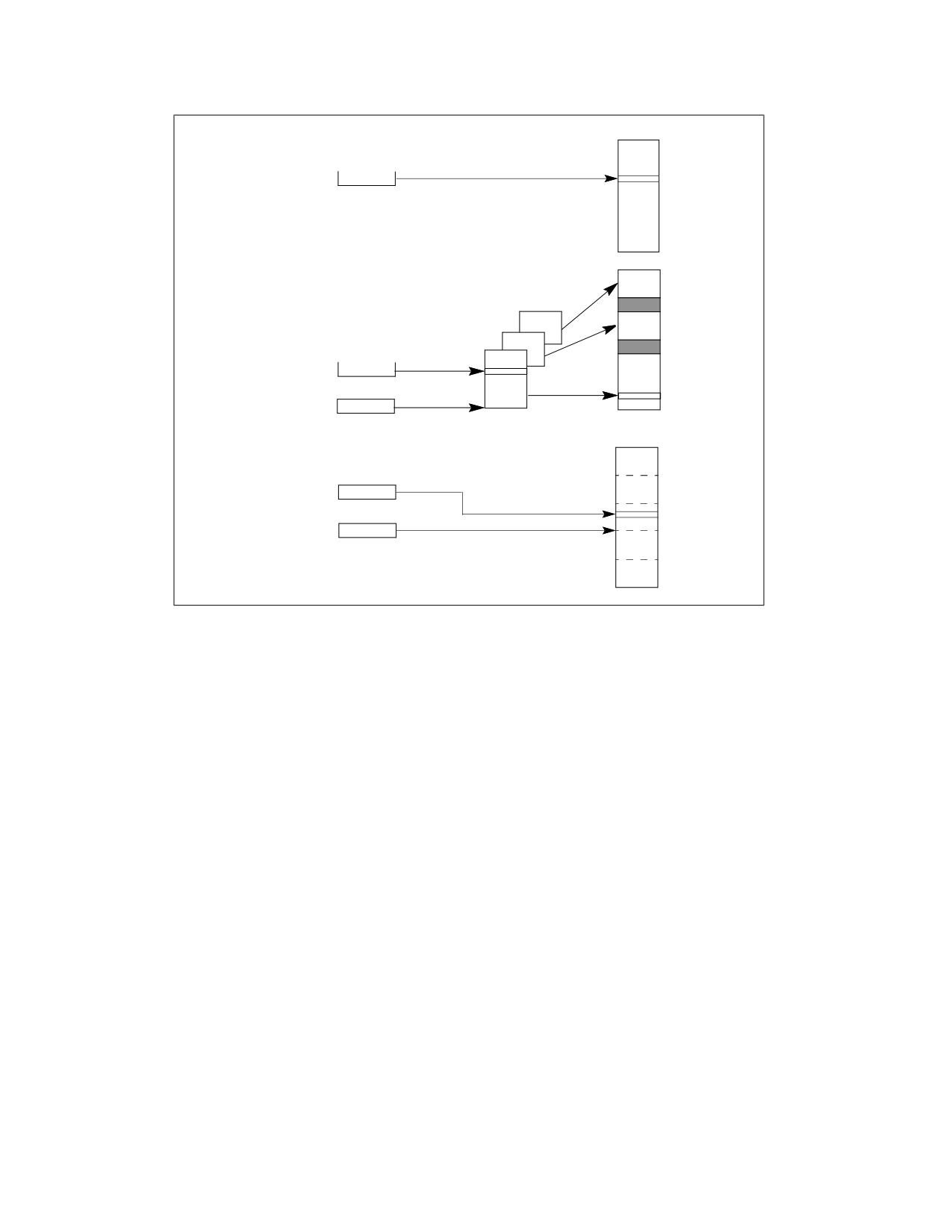
• Flat memory model - Memory appears to a program as a single, continuous address space (Figure 3-3). This
space is called a linear address space. Code, data, and stacks are all contained in this address space. Linear
address space is byte addressable, with addresses running contiguously from 0 to 232 - 1 (if not in 64-bit
mode). An address for any byte in linear address space is called a linear address.
• Segmented memory model - Memory appears to a program as a group of independent address spaces
called segments. Code, data, and stacks are typically contained in separate segments. To address a byte in a
segment, a program issues a logical address. This consists of a segment selector and an offset (logical
addresses are often referred to as far pointers). The segment selector identifies the segment to be accessed
and the offset identifies a byte in the address space of the segment. Programs running on an IA-32 processor
can address up to 16,383 segments of different sizes and types, and each segment can be as large as 232
bytes.
Internally, all the segments that are defined for a system are mapped into the processor’s linear address space.
To access a memory location, the processor thus translates each logical address into a linear address. This
translation is transparent to the application program.
The primary reason for using segmented memory is to increase the reliability of programs and systems. For
example, placing a program’s stack in a separate segment prevents the stack from growing into the code or
data space and overwriting instructions or data, respectively.
• Real-address mode memory model - This is the memory model for the Intel 8086 processor. It is
supported to provide compatibility with existing programs written to run on the Intel 8086 processor. The real-
address mode uses a specific implementation of segmented memory in which the linear address space for the
program and the operating system/executive consists of an array of segments of up to 64 KBytes in size each.
The maximum size of the linear address space in real-address mode is 220 bytes.
See also: Chapter 23, “8086 Emulation,” in the Intel® 64 and IA-32 Architectures Software Developer’s
Manual, Volume 3B.
Vol. 1
3-7
BASIC EXECUTION ENVIRONMENT
Flat Model
Linear Address
Linear
Address
Space*
Segmented Model
Segments
Linear
Offset (effective address)
Address
Space*
Logical
Segment Selector
Address
Real-Address Mode Model
Linear Address
Offset
Space Divided
Into Equal
Sized Segments
Logical
Segment Selector
Address
* The linear address space
can be paged when using the
flat or segmented model.
Figure 3-3. Three Memory Management Models
3.3.2
Paging and Virtual Memory
With the flat or the segmented memory model, linear address space is mapped into the processor’s physical
address space either directly or through paging. When using direct mapping (paging disabled), each linear address
has a one-to-one correspondence with a physical address. Linear addresses are sent out on the processor’s address
lines without translation.
When using the IA-32 architecture’s paging mechanism (paging enabled), linear address space is divided into
pages which are mapped to virtual memory. The pages of virtual memory are then mapped as needed into physical
memory. When an operating system or executive uses paging, the paging mechanism is transparent to an applica-
tion program. All that the application sees is linear address space.
In addition, IA-32 architecture’s paging mechanism includes extensions that support:
• Physical Address Extensions (PAE) to address physical address space greater than 4 GBytes.
• Page Size Extensions (PSE) to map linear address to physical address in 4-MBytes pages.
See also: Chapter 3, “Protected-Mode Memory Management,” in the Intel® 64 and IA-32 Architectures Software
Developer’s Manual, Volume 3A.
3.3.3
Memory Organization in 64-Bit Mode
Intel 64 architecture supports physical address space greater than 64 GBytes; the actual physical address size of
IA-32 processors is implementation specific. In 64-bit mode, there is architectural support for 64-bit linear address
space. However, processors supporting Intel 64 architecture may implement less than 64-bits (see Section
3.3.7.1). The linear address space is mapped into the processor physical address space through the PAE paging
mechanism.
3-8
Vol. 1
BASIC EXECUTION ENVIRONMENT
3.3.4
Modes of Operation vs. Memory Model
When writing code for an IA-32 or Intel 64 processor, a programmer needs to know the operating mode the
processor is going to be in when executing the code and the memory model being used. The relationship between
operating modes and memory models is as follows:
• Protected mode - When in protected mode, the processor can use any of the memory models described in
this section. (The real-addressing mode memory model is ordinarily used only when the processor is in the
virtual-8086 mode.) The memory model used depends on the design of the operating system or executive.
When multitasking is implemented, individual tasks can use different memory models.
• Real-address mode - When in real-address mode, the processor only supports the real-address mode
memory model.
• System management mode - When in SMM, the processor switches to a separate address space, called the
system management RAM (SMRAM). The memory model used to address bytes in this address space is similar
to the real-address mode model. See Chapter 34, “System Management Mode,” in the Intel® 64 and IA-32
Architectures Software Developer’s Manual, Volume 3C, for more information on the memory model used in
SMM.
• Compatibility mode - Software that needs to run in compatibility mode should observe the same memory
model as those targeted to run in 32-bit protected mode. The effect of segmentation is the same as it is in 32-
bit protected mode semantics.
•
64-bit mode - Segmentation is generally (but not completely) disabled, creating a flat 64-bit linear-address
space. Specifically, the processor treats the segment base of CS, DS, ES, and SS as zero in 64-bit mode (this
makes a linear address equal an effective address). Segmented and real address modes are not available in 64-
bit mode.
3.3.5
32-Bit and 16-Bit Address and Operand Sizes
IA-32 processors in protected mode can be configured for 32-bit or 16-bit address and operand sizes. With 32-bit
address and operand sizes, the maximum linear address or segment offset is FFFFFFFFH (232-1); operand sizes are
typically 8 bits or 32 bits. With 16-bit address and operand sizes, the maximum linear address or segment offset is
FFFFH (216-1); operand sizes are typically 8 bits or 16 bits.
When using 32-bit addressing, a logical address (or far pointer) consists of a 16-bit segment selector and a 32-bit
offset; when using 16-bit addressing, an address consists of a 16-bit segment selector and a 16-bit offset.
Instruction prefixes allow temporary overrides of the default address and/or operand sizes from within a program.
When operating in protected mode, the segment descriptor for the currently executing code segment defines the
default address and operand size. A segment descriptor is a system data structure not normally visible to applica-
tion code. Assembler directives allow the default addressing and operand size to be chosen for a program. The
assembler and other tools then set up the segment descriptor for the code segment appropriately.
When operating in real-address mode, the default addressing and operand size is 16 bits. An address-size override
can be used in real-address mode to enable 32-bit addressing. However, the maximum allowable 32-bit linear
address is still 000FFFFFH (220-1).
3.3.6
Extended Physical Addressing in Protected Mode
Beginning with P6 family processors, the IA-32 architecture supports addressing of up to 64 GBytes (236 bytes) of
physical memory. A program or task could not address locations in this address space directly. Instead, it
addresses individual linear address spaces of up to 4 GBytes that mapped to 64-GByte physical address space
through a virtual memory management mechanism. Using this mechanism, an operating system can enable a
program to switch 4-GByte linear address spaces within 64-GByte physical address space.
The use of extended physical addressing requires the processor to operate in protected mode and the operating
system to provide a virtual memory management system. See “36-Bit Physical Addressing Using the PAE Paging
Mechanism” in Chapter 3, “Protected-Mode Memory Management,” in the Intel® 64 and IA-32 Architectures Soft-
ware Developer’s Manual, Volume 3A.
Vol. 1
3-9

BASIC EXECUTION ENVIRONMENT
3.3.7
Address Calculations in 64-Bit Mode
In most cases, 64-bit mode uses flat address space for code, data, and stacks. In 64-bit mode (if there is no
address-size override), the size of effective address calculations is 64 bits. An effective-address calculation uses a
64-bit base and index registers and sign-extend displacements to 64 bits.
In the flat address space of 64-bit mode, linear addresses are equal to effective addresses because the base
address is zero. In the event that FS or GS segments are used with a non-zero base, this rule does not hold. In 64-
bit mode, the effective address components are added and the effective address is truncated (See for example the
instruction LEA) before adding the full 64-bit segment base. The base is never truncated, regardless of addressing
mode in 64-bit mode.
The instruction pointer is extended to 64 bits to support 64-bit code offsets. The 64-bit instruction pointer is called
the RIP. Table 3-1 shows the relationship between RIP, EIP, and IP.
Table 3-1. Instruction Pointer Sizes
Bits 63:32
Bits 31:16
Bits 15:0
16-bit instruction pointer
Not Modified
IP
32-bit instruction pointer
Zero Extension
EIP
64-bit instruction pointer
RIP
Generally, displacements and immediates in 64-bit mode are not extended to 64 bits. They are still limited to 32
bits and sign-extended during effective-address calculations. In 64-bit mode, however, support is provided for 64-
bit displacement and immediate forms of the MOV instruction.
All 16-bit and 32-bit address calculations are zero-extended in IA-32e mode to form 64-bit addresses. Address
calculations are first truncated to the effective address size of the current mode (64-bit mode or compatibility
mode), as overridden by any address-size prefix. The result is then zero-extended to the full 64-bit address width.
Because of this, 16-bit and 32-bit applications running in compatibility mode can access only the low 4 GBytes of
the 64-bit mode effective addresses. Likewise, a 32-bit address generated in 64-bit mode can access only the low
4 GBytes of the 64-bit mode effective addresses.
3.3.7.1
Canonical Addressing
In 64-bit mode, an address is considered to be in canonical form if address bits 63 through to the most-significant
implemented bit by the microarchitecture are set to either all ones or all zeros.
Intel 64 architecture defines a 64-bit linear address. Implementations can support less. The first implementation of
IA-32 processors with Intel 64 architecture supports a 48-bit linear address. This means a canonical address must
have bits 63 through 48 set to zeros or ones (depending on whether bit 47 is a zero or one).
Although implementations may not use all 64 bits of the linear address, they should check bits 63 through the
most-significant implemented bit to see if the address is in canonical form. If a linear-memory reference is not in
canonical form, the implementation should generate an exception. In most cases, a general-protection exception
(#GP) is generated. However, in the case of explicit or implied stack references, a stack fault (#SS) is generated.
Instructions that have implied stack references, by default, use the SS segment register. These include PUSH/POP-
related instructions and instructions using RSP/RBP as base registers. In these cases, the canonical fault is #SS.
If an instruction uses base registers RSP/RBP and uses a segment override prefix to specify a non-SS segment, a
canonical fault generates a #GP (instead of an #SS). In 64-bit mode, only FS and GS segment-overrides are appli-
cable in this situation. Other segment override prefixes (CS, DS, ES, and SS) are ignored. Note that this also means
that an SS segment-override applied to a “non-stack” register reference is ignored. Such a sequence still produces
a #GP for a canonical fault (and not an #SS).
3.4
BASIC PROGRAM EXECUTION REGISTERS
IA-32 architecture provides 16 basic program execution registers for use in general system and application
programing (see Figure 3-4). These registers can be grouped as follows:
3-10
Vol. 1

BASIC EXECUTION ENVIRONMENT
• General-purpose registers. These eight registers are available for storing operands and pointers.
• Segment registers. These registers hold up to six segment selectors.
• EFLAGS (program status and control) register. The EFLAGS register report on the status of the program
being executed and allows limited (application-program level) control of the processor.
• EIP (instruction pointer) register. The EIP register contains a 32-bit pointer to the next instruction to be
executed.
3.4.1
General-Purpose Registers
The 32-bit general-purpose registers EAX, EBX, ECX, EDX, ESI, EDI, EBP, and ESP are provided for holding the
following items:
• Operands for logical and arithmetic operations.
• Operands for address calculations.
• Memory pointers.
Although all of these registers are available for general storage of operands, results, and pointers, caution should
be used when referencing the ESP register. The ESP register holds the stack pointer and as a general rule should
not be used for another purpose.
Many instructions assign specific registers to hold operands. For example, string instructions use the contents of
the ECX, ESI, and EDI registers as operands. When using a segmented memory model, some instructions assume
that pointers in certain registers are relative to specific segments. For instance, some instructions assume that a
pointer in the EBX register points to a memory location in the DS segment.
General-Purpose Registers
31
0
EAX
EBX
ECX
EDX
ESI
EDI
EBP
ESP
Segment Registers
15
0
CS
DS
SS
ES
FS
GS
Program Status and Control Register
31
0
EFLAGS
Instruction Pointer
31
0
EIP
Figure 3-4. General System and Application Programming Registers
Vol. 1
3-11

BASIC EXECUTION ENVIRONMENT
The special uses of general-purpose registers by instructions are described in Chapter 5, “Instruction Set
Summary,” in this volume. See also: Chapter 3, Chapter 4, Chapter 5, and Chapter 6 of the Intel® 64 and IA-32
Architectures Software Developer’s Manual, Volumes 2A, 2B, 2C, & 2D. The following is a summary of special uses:
• EAX - Accumulator for operands and results data.
• EBX - Pointer to data in the DS segment.
• ECX - Counter for string and loop operations.
• EDX - I/O pointer.
• ESI - Pointer to data in the segment pointed to by the DS register; source pointer for string operations.
• EDI - Pointer to data (or destination) in the segment pointed to by the ES register; destination pointer for
string operations.
• ESP - Stack pointer (in the SS segment).
• EBP - Pointer to data on the stack (in the SS segment).
As shown in Figure 3-5, the lower 16 bits of the general-purpose registers map directly to the register set found in
the 8086 and Intel 286 processors and can be referenced with the names AX, BX, CX, DX, BP, SI, DI, and SP. Each
of the lower two bytes of the EAX, EBX, ECX, and EDX registers can be referenced by the names AH, BH, CH, and
DH (high bytes) and AL, BL, CL, and DL (low bytes).
General-Purpose Registers
31
1615
8
7
0
16-bit
32-bit
AH
AL
AX
EAX
BH
BL
BX
EBX
CH
CL
CX
ECX
DH
DL
DX
EDX
BP
EBP
SI
ESI
DI
EDI
SP
ESP
Figure 3-5. Alternate General-Purpose Register Names
3.4.1.1
General-Purpose Registers in 64-Bit Mode
In 64-bit mode, there are 16 general purpose registers and the default operand size is 32 bits. However, general-
purpose registers are able to work with either 32-bit or 64-bit operands. If a 32-bit operand size is specified: EAX,
EBX, ECX, EDX, EDI, ESI, EBP, ESP, R8D - R15D are available. If a 64-bit operand size is specified: RAX, RBX, RCX,
RDX, RDI, RSI, RBP, RSP, R8-R15 are available. R8D-R15D/R8-R15 represent eight new general-purpose registers.
All of these registers can be accessed at the byte, word, dword, and qword level. REX prefixes are used to generate
64-bit operand sizes or to reference registers R8-R15.
Registers only available in 64-bit mode (R8-R15 and XMM8-XMM15) are preserved across transitions from 64-bit
mode into compatibility mode then back into 64-bit mode. However, values of R8-R15 and XMM8-XMM15 are unde-
fined after transitions from 64-bit mode through compatibility mode to legacy or real mode and then back through
compatibility mode to 64-bit mode.
3-12
Vol. 1

BASIC EXECUTION ENVIRONMENT
Table 3-2. Addressable General Purpose Registers
Register Type
Without REX
With REX
Byte Registers
AL, BL, CL, DL, AH, BH, CH, DH
AL, BL, CL, DL, DIL, SIL, BPL, SPL, R8B - R15B
Word Registers
AX, BX, CX, DX, DI, SI, BP, SP
AX, BX, CX, DX, DI, SI, BP, SP, R8W - R15W
Doubleword Registers
EAX, EBX, ECX, EDX, EDI, ESI, EBP, ESP
EAX, EBX, ECX, EDX, EDI, ESI, EBP, ESP, R8D - R15D
Quadword Registers
N.A.
RAX, RBX, RCX, RDX, RDI, RSI, RBP, RSP, R8 - R15
In 64-bit mode, there are limitations on accessing byte registers. An instruction cannot reference legacy high-
bytes (for example: AH, BH, CH, DH) and one of the new byte registers at the same time (for example: the low
byte of the RAX register). However, instructions may reference legacy low-bytes (for example: AL, BL, CL, or DL)
and new byte registers at the same time (for example: the low byte of the R8 register, or RBP). The architecture
enforces this limitation by changing high-byte references (AH, BH, CH, DH) to low byte references (BPL, SPL, DIL,
SIL: the low 8 bits for RBP, RSP, RDI, and RSI) for instructions using a REX prefix.
When in 64-bit mode, operand size determines the number of valid bits in the destination general-purpose
register:
•
64-bit operands generate a 64-bit result in the destination general-purpose register.
•
32-bit operands generate a 32-bit result, zero-extended to a 64-bit result in the destination general-purpose
register.
•
8-bit and 16-bit operands generate an 8-bit or 16-bit result. The upper 56 bits or 48 bits (respectively) of the
destination general-purpose register are not modified by the operation. If the result of an 8-bit or 16-bit
operation is intended for 64-bit address calculation, explicitly sign-extend the register to the full 64-bits.
Because the upper 32 bits of 64-bit general-purpose registers are undefined in 32-bit modes, the upper 32 bits of
any general-purpose register are not preserved when switching from 64-bit mode to a 32-bit mode (to protected
mode or compatibility mode). Software must not depend on these bits to maintain a value after a 64-bit to 32-bit
mode switch.
3.4.2
Segment Registers
The segment registers (CS, DS, SS, ES, FS, and GS) hold 16-bit segment selectors. A segment selector is a special
pointer that identifies a segment in memory. To access a particular segment in memory, the segment selector for
that segment must be present in the appropriate segment register.
When writing application code, programmers generally create segment selectors with assembler directives and
symbols. The assembler and other tools then create the actual segment selector values associated with these
directives and symbols. If writing system code, programmers may need to create segment selectors directly. See
Chapter 3, “Protected-Mode Memory Management,” in the Intel® 64 and IA-32 Architectures Software Developer’s
Manual, Volume 3A.
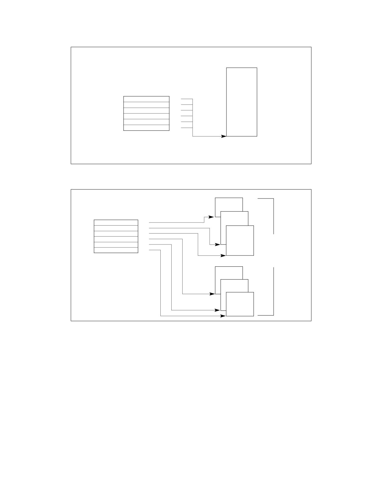
How segment registers are used depends on the type of memory management model that the operating system or
executive is using. When using the flat (unsegmented) memory model, segment registers are loaded with segment
selectors that point to overlapping segments, each of which begins at address 0 of the linear address space (see
Figure 3-6). These overlapping segments then comprise the linear address space for the program. Typically, two
overlapping segments are defined: one for code and another for data and stacks. The CS segment register points
to the code segment and all the other segment registers point to the data and stack segment.
When using the segmented memory model, each segment register is ordinarily loaded with a different segment
selector so that each segment register points to a different segment within the linear address space (see
Figure 3-7). At any time, a program can thus access up to six segments in the linear address space. To access a
segment not pointed to by one of the segment registers, a program must first load the segment selector for the
segment to be accessed into a segment register.
Vol. 1
3-13
BASIC EXECUTION ENVIRONMENT
Linear Address
Space for Program
Segment Registers
Overlapping
Segments
of up to
CS
4 GBytes
DS
Beginning at
SS
Address 0
ES
FS
GS
The segment selector in
each segment register
points to an overlapping
segment in the linear
address space.
Figure 3-6. Use of Segment Registers for Flat Memory Model
Code
Segment
Segment Registers
Data
Segment
CS
DS
Stack
SS
Segment
ES
All segments
FS
are mapped
GS
to the same
linear-address
space
Data
Segment
Data
Segment
Data
Segment
Figure 3-7. Use of Segment Registers in Segmented Memory Model
Each of the segment registers is associated with one of three types of storage: code, data, or stack. For example,
the CS register contains the segment selector for the code segment, where the instructions being executed are
stored. The processor fetches instructions from the code segment, using a logical address that consists of the
segment selector in the CS register and the contents of the EIP register. The EIP register contains the offset within
the code segment of the next instruction to be executed. The CS register cannot be loaded explicitly by an applica-
tion program. Instead, it is loaded implicitly by instructions or internal processor operations that change program
control (such as procedure calls, interrupt handling, or task switching).
The DS, ES, FS, and GS registers point to four data segments. The availability of four data segments permits effi-
cient and secure access to different types of data structures. For example, four separate data segments might be
created: one for the data structures of the current module, another for the data exported from a higher-level
module, a third for a dynamically created data structure, and a fourth for data shared with another program. To
access additional data segments, the application program must load segment selectors for these segments into the
DS, ES, FS, and GS registers, as needed.
The SS register contains the segment selector for the stack segment, where the procedure stack is stored for the
program, task, or handler currently being executed. All stack operations use the SS register to find the stack
3-14
Vol. 1
BASIC EXECUTION ENVIRONMENT
segment. Unlike the CS register, the SS register can be loaded explicitly, which permits application programs to set
up multiple stacks and switch among them.
See Section 3.3, “Memory Organization,” for an overview of how the segment registers are used in real-address
mode.
The four segment registers CS, DS, SS, and ES are the same as the segment registers found in the Intel 8086 and
Intel 286 processors and the FS and GS registers were introduced into the IA-32 Architecture with the Intel386™
family of processors.
3.4.2.1
Segment Registers in 64-Bit Mode
In 64-bit mode: CS, DS, ES, SS are treated as if each segment base is 0, regardless of the value of the associated
segment descriptor base. This creates a flat address space for code, data, and stack. FS and GS are exceptions.
Both segment registers may be used as additional base registers in linear address calculations (in the addressing
of local data and certain operating system data structures).
Even though segmentation is generally disabled, segment register loads may cause the processor to perform
segment access assists. During these activities, enabled processors will still perform most of the legacy checks on
loaded values (even if the checks are not applicable in 64-bit mode). Such checks are needed because a segment
register loaded in 64-bit mode may be used by an application running in compatibility mode.
Limit checks for CS, DS, ES, SS, FS, and GS are disabled in 64-bit mode.
3.4.3
EFLAGS Register
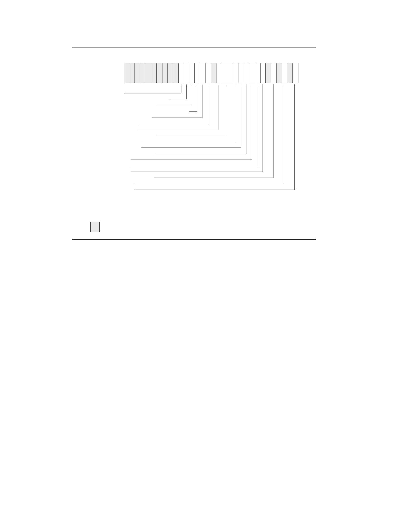
The 32-bit EFLAGS register contains a group of status flags, a control flag, and a group of system flags. Figure 3-8
defines the flags within this register. Following initialization of the processor (either by asserting the RESET pin or
the INIT pin), the state of the EFLAGS register is 00000002H. Bits 1, 3, 5, 15, and 22 through 31 of this register
are reserved. Software should not use or depend on the states of any of these bits.
Some of the flags in the EFLAGS register can be modified directly, using special-purpose instructions (described in
the following sections). There are no instructions that allow the whole register to be examined or modified directly.
The following instructions can be used to move groups of flags to and from the procedure stack or the EAX register:
LAHF, SAHF, PUSHF, PUSHFD, POPF, and POPFD. After the contents of the EFLAGS register have been transferred to
the procedure stack or EAX register, the flags can be examined and modified using the processor’s bit manipulation
instructions (BT, BTS, BTR, and BTC).
When suspending a task (using the processor’s multitasking facilities), the processor automatically saves the state
of the EFLAGS register in the task state segment (TSS) for the task being suspended. When binding itself to a new
task, the processor loads the EFLAGS register with data from the new task’s TSS.
When a call is made to an interrupt or exception handler procedure, the processor automatically saves the state of
the EFLAGS registers on the procedure stack. When an interrupt or exception is handled with a task switch, the
state of the EFLAGS register is saved in the TSS for the task being suspended.
Vol. 1
3-15
BASIC EXECUTION ENVIRONMENT
31 30 29 28 27 26 25 24 23 22 21 20 19 18 17 16
15 14 13 12 11 10 9
8
7
6
5
4
3
2
1
0
I
V
V
I
A
V
R
N
O
O
D
I
T
S
Z
A
P
C
0
0
0
0
0
0
0
0
0
0
I
I
0
0
0
1
D
C
M
F
T
P
F
F
F
F
F
F
F
F
F
P
F
L
X ID Flag (ID)
X Virtual Interrupt Pending (VIP)
X Virtual Interrupt Flag (VIF)
X Alignment Check / Access Control (AC)
X Virtual-8086 Mode (VM)
X Resume Flag (RF)
X Nested Task (NT)
X I/O Privilege Level (IOPL)
S Overflow Flag (OF)
C Direction Flag (DF)
X Interrupt Enable Flag (IF)
X Trap Flag (TF)
S Sign Flag (SF)
S Zero Flag (ZF)
S Auxiliary Carry Flag (AF)
S Parity Flag (PF)
S Carry Flag (CF)
S Indicates a Status Flag
C Indicates a Control Flag
X Indicates a System Flag
Reserved bit positions. DO NOT USE.
Always set to values previously read.
Figure 3-8. EFLAGS Register
As the IA-32 Architecture has evolved, flags have been added to the EFLAGS register, but the function and place-
ment of existing flags have remained the same from one family of the IA-32 processors to the next. As a result,
code that accesses or modifies these flags for one family of IA-32 processors works as expected when run on later
families of processors.
3.4.3.1
Status Flags
The status flags (bits 0, 2, 4, 6, 7, and 11) of the EFLAGS register indicate the results of arithmetic instructions,
such as the ADD, SUB, MUL, and DIV instructions. The status flag functions are:
CF (bit 0)
Carry flag - Set if an arithmetic operation generates a carry or a borrow out of the most-
significant bit of the result; cleared otherwise. This flag indicates an overflow condition for
unsigned-integer arithmetic. It is also used in multiple-precision arithmetic.
PF (bit 2)
Parity flag - Set if the least-significant byte of the result contains an even number of 1 bits;
cleared otherwise.
AF (bit 4)
Auxiliary Carry flag - Set if an arithmetic operation generates a carry or a borrow out of bit
3 of the result; cleared otherwise. This flag is used in binary-coded decimal (BCD) arithmetic.
ZF (bit 6)
Zero flag - Set if the result is zero; cleared otherwise.
SF (bit 7)
Sign flag - Set equal to the most-significant bit of the result, which is the sign bit of a signed
integer. (0 indicates a positive value and 1 indicates a negative value.)
OF (bit 11)
Overflow flag - Set if the integer result is too large a positive number or too small a negative
number (excluding the sign-bit) to fit in the destination operand; cleared otherwise. This flag
indicates an overflow condition for signed-integer (two’s complement) arithmetic.
Of these status flags, only the CF flag can be modified directly, using the STC, CLC, and CMC instructions. Also the
bit instructions (BT, BTS, BTR, and BTC) copy a specified bit into the CF flag.
3-16
Vol. 1
BASIC EXECUTION ENVIRONMENT
The status flags allow a single arithmetic operation to produce results for three different data types: unsigned inte-
gers, signed integers, and BCD integers. If the result of an arithmetic operation is treated as an unsigned integer,
the CF flag indicates an out-of-range condition (carry or a borrow); if treated as a signed integer (two’s comple-
ment number), the OF flag indicates a carry or borrow; and if treated as a BCD digit, the AF flag indicates a carry
or borrow. The SF flag indicates the sign of a signed integer. The ZF flag indicates either a signed- or an unsigned-
integer zero.
When performing multiple-precision arithmetic on integers, the CF flag is used in conjunction with the add with
carry (ADC) and subtract with borrow (SBB) instructions to propagate a carry or borrow from one computation to
the next.
The condition instructions Jcc (jump on condition code cc), SETcc (byte set on condition code cc), LOOPcc, and
CMOVcc (conditional move) use one or more of the status flags as condition codes and test them for branch, set-
byte, or end-loop conditions.
3.4.3.2
DF Flag
The direction flag (DF, located in bit 10 of the EFLAGS register) controls string instructions (MOVS, CMPS, SCAS,
LODS, and STOS). Setting the DF flag causes the string instructions to auto-decrement (to process strings from
high addresses to low addresses). Clearing the DF flag causes the string instructions to auto-increment
(process strings from low addresses to high addresses).
The STD and CLD instructions set and clear the DF flag, respectively.
3.4.3.3
System Flags and IOPL Field
The system flags and IOPL field in the EFLAGS register control operating-system or executive operations. They
should not be modified by application programs. The functions of the system flags are as follows:
TF (bit 8)
Trap flag - Set to enable single-step mode for debugging; clear to disable single-step mode.
IF (bit 9)
Interrupt enable flag - Controls the response of the processor to maskable interrupt
requests. Set to respond to maskable interrupts; cleared to inhibit maskable interrupts.
IOPL (bits 12 and 13)
I/O privilege level field - Indicates the I/O privilege level of the currently running program
or task. The current privilege level (CPL) of the currently running program or task must be less
than or equal to the I/O privilege level to access the I/O address space. The POPF and IRET
instructions can modify this field only when operating at a CPL of 0.
NT (bit 14)
Nested task flag - Controls the chaining of interrupted and called tasks. Set when the
current task is linked to the previously executed task; cleared when the current task is not
linked to another task.
RF (bit 16)
Resume flag - Controls the processor’s response to debug exceptions.
VM (bit 17)
Virtual-8086 mode flag - Set to enable virtual-8086 mode; clear to return to protected
mode without virtual-8086 mode semantics.
AC (bit 18)
Alignment check (or access control) flag - If the AM bit is set in the CR0 register, align-
ment checking of user-mode data accesses is enabled if and only if this flag is 1.
If the SMAP bit is set in the CR4 register, explicit supervisor-mode data accesses to user-mode
pages are allowed if and only if this bit is 1. See Section 5.6, “Access Rights,” in the Intel® 64
and IA-32 Architectures Software Developer’s Manual, Volume 3A.
VIF (bit 19)
Virtual interrupt flag - Virtual image of the IF flag. Used in conjunction with the VIP flag.
(To use this flag and the VIP flag the virtual mode extensions are enabled by setting the VME
flag in control register CR4.)
VIP (bit 20)
Virtual interrupt pending flag - Set to indicate that an interrupt is pending; clear when no
interrupt is pending. (Software sets and clears this flag; the processor only reads it.) Used in
conjunction with the VIF flag.
ID (bit 21)
Identification flag - The ability of a program to set or clear this flag indicates support for
the CPUID instruction.
Vol. 1
3-17
BASIC EXECUTION ENVIRONMENT
For a detailed description of these flags: see Chapter 3, “Protected-Mode Memory Management,” in the Intel® 64
and IA-32 Architectures Software Developer’s Manual, Volume 3A.
3.4.3.4
RFLAGS Register in 64-Bit Mode
In 64-bit mode, EFLAGS is extended to 64 bits and called RFLAGS. The upper 32 bits of RFLAGS register is
reserved. The lower 32 bits of RFLAGS is the same as EFLAGS.
3.5
INSTRUCTION POINTER
The instruction pointer (EIP) register contains the offset in the current code segment for the next instruction to be
executed. It is advanced from one instruction boundary to the next in straight-line code or it is moved ahead or
backwards by a number of instructions when executing JMP, Jcc, CALL, RET, and IRET instructions.
The EIP register cannot be accessed directly by software; it is controlled implicitly by control-transfer instructions
(such as JMP, Jcc, CALL, and RET), interrupts, and exceptions. The only way to read the EIP register is to execute a
CALL instruction and then read the value of the return instruction pointer from the procedure stack. The EIP
register can be loaded indirectly by modifying the value of a return instruction pointer on the procedure stack and
executing a return instruction (RET or IRET). See Section 6.2.4.2, “Return Instruction Pointer.”
All IA-32 processors prefetch instructions. Because of instruction prefetching, an instruction address read from the
bus during an instruction load does not match the value in the EIP register. Even though different processor gener-
ations use different prefetching mechanisms, the function of the EIP register to direct program flow remains fully
compatible with all software written to run on IA-32 processors.
3.5.1
Instruction Pointer in 64-Bit Mode
In 64-bit mode, the RIP register becomes the instruction pointer. This register holds the 64-bit offset of the next
instruction to be executed. 64-bit mode also supports a technique called RIP-relative addressing. Using this tech-
nique, the effective address is determined by adding a displacement to the RIP of the next instruction.
3.6
OPERAND-SIZE AND ADDRESS-SIZE ATTRIBUTES
When the processor is executing in protected mode, every code segment has a default operand-size attribute and
address-size attribute. These attributes are selected with the D (default size) flag in the segment descriptor for the
code segment (see Chapter 3, “Protected-Mode Memory Management,” in the Intel® 64 and IA-32 Architectures
Software Developer’s Manual, Volume 3A). When the D flag is set, the 32-bit operand-size and address-size attri-
butes are selected; when the flag is clear, the 16-bit size attributes are selected. When the processor is executing
in real-address mode, virtual-8086 mode, or SMM, the default operand-size and address-size attributes are always
16 bits.
The operand-size attribute selects the size of operands. When the 16-bit operand-size attribute is in force, oper-
ands can generally be either 8 bits or 16 bits, and when the 32-bit operand-size attribute is in force, operands can
generally be 8 bits or 32 bits.
The address-size attribute selects the sizes of addresses used to address memory: 16 bits or 32 bits. When the 16-
bit address-size attribute is in force, segment offsets and displacements are 16 bits. This restriction limits the size
of a segment to 64 KBytes. When the 32-bit address-size attribute is in force, segment offsets and displacements
are 32 bits, allowing up to 4 GBytes to be addressed.
The default operand-size attribute and/or address-size attribute can be overridden for a particular instruction by
adding an operand-size and/or address-size prefix to an instruction. See Chapter 2, “Instruction Format,” in the
Intel® 64 and IA-32 Architectures Software Developer’s Manual, Volume 2A. The effect of this prefix applies only to
the targeted instruction.
Table 3-4 shows effective operand size and address size (when executing in protected mode or compatibility mode)
depending on the settings of the D flag and the operand-size and address-size prefixes.
3-18
Vol. 1

BASIC EXECUTION ENVIRONMENT
Table 3-3. Effective Operand- and Address-Size Attributes
D Flag in Code Segment Descriptor
0
0
0
0
1
1
1
1
Operand-Size Prefix 66H
N
N
Y
Y
N
N
Y
Y
Address-Size Prefix 67H
N
Y
N
Y
N
Y
N
Y
Effective Operand Size
16
16
32
32
32
32
16
16
Effective Address Size
16
32
16
32
32
16
32
16
NOTES:
Y: Yes - this instruction prefix is present.
N: No - this instruction prefix is not present.
3.6.1
Operand Size and Address Size in 64-Bit Mode
In 64-bit mode, the default address size is 64 bits and the default operand size is 32 bits. Defaults can be over-
ridden using prefixes. Address-size and operand-size prefixes allow mixing of 32/64-bit data and 32/64-bit
addresses on an instruction-by-instruction basis. Table 3-4 shows valid combinations of the 66H instruction prefix
and the REX.W prefix that may be used to specify operand-size overrides in 64-bit mode. Note that 16-bit
addresses are not supported in 64-bit mode.
REX prefixes consist of 4-bit fields that form 16 different values. The W-bit field in the REX prefixes is referred to as
REX.W. If the REX.W field is properly set, the prefix specifies an operand size override to 64 bits. Note that software
can still use the operand-size 66H prefix to toggle to a 16-bit operand size. However, setting REX.W takes prece-
dence over the operand-size prefix (66H) when both are used.
In the case of SSE/SSE2/SSE3/SSSE3 SIMD instructions: the 66H, F2H, and F3H prefixes are mandatory for
opcode extensions. In such a case, there is no interaction between a valid REX.W prefix and a 66H opcode exten-
sion prefix.
See Chapter 2, “Instruction Format,” in the Intel® 64 and IA-32 Architectures Software Developer’s Manual,
Volume 2A.
Table 3-4. Effective Operand- and Address-Size Attributes in 64-Bit Mode
L Flag in Code Segment Descriptor
1
1
1
1
1
1
1
1
REX.W Prefix
0
0
0
0
1
1
1
1
Operand-Size Prefix 66H
N
N
Y
Y
N
N
Y
Y
Address-Size Prefix 67H
N
Y
N
Y
N
Y
N
Y
Effective Operand Size
32
32
16
16
64
64
64
64
Effective Address Size
64
32
64
32
64
32
64
32
NOTES:
Y: Yes - this instruction prefix is present.
N: No - this instruction prefix is not present.
3.7
OPERAND ADDRESSING
IA-32 machine-instructions act on zero or more operands. Some operands are specified explicitly and others are
implicit. The data for a source operand can be located in:
• The instruction itself (an immediate operand).
• A register.
• A memory location.
• An I/O port.
Vol. 1
3-19
BASIC EXECUTION ENVIRONMENT
When an instruction returns data to a destination operand, it can be returned to:
• A register.
• A memory location.
• An I/O port.
3.7.1
Immediate Operands
Some instructions use data encoded in the instruction itself as a source operand. These operands are called imme-
diate operands (or simply immediates). For example, the following ADD instruction adds an immediate value of 14
to the contents of the EAX register:
ADD EAX, 14
All arithmetic instructions (except the DIV and IDIV instructions) allow the source operand to be an immediate
value. The maximum value allowed for an immediate operand varies among instructions, but can never be greater
than the maximum value of an unsigned doubleword integer (232).
3.7.2
Register Operands
Source and destination operands can be any of the following registers, depending on the instruction being
executed:
•
32-bit general-purpose registers (EAX, EBX, ECX, EDX, ESI, EDI, ESP, or EBP).
•
16-bit general-purpose registers (AX, BX, CX, DX, SI, DI, SP, or BP).
•
8-bit general-purpose registers (AH, BH, CH, DH, AL, BL, CL, or DL).
• Segment registers (CS, DS, SS, ES, FS, and GS).
• EFLAGS register.
• X87 FPU registers (ST0 through ST7, status word, control word, tag word, data operand pointer, and instruction
pointer).
• MMX registers (MM0 through MM7).
• XMM registers (XMM0 through XMM7) and the MXCSR register.
• Control registers (CR0, CR2, CR3, and CR4) and system table pointer registers (GDTR, LDTR, IDTR, and task
register).
• Debug registers (DR0, DR1, DR2, DR3, DR6, and DR7).
• MSR registers.
Some instructions (such as the DIV and MUL instructions) use quadword operands contained in a pair of 32-bit
registers. Register pairs are represented with a colon separating them. For example, in the register pair EDX:EAX,
EDX contains the high order bits and EAX contains the low order bits of a quadword operand.
Several instructions (such as the PUSHFD and POPFD instructions) are provided to load and store the contents of
the EFLAGS register or to set or clear individual flags in this register. Other instructions (such as the Jcc instruc-
tions) use the state of the status flags in the EFLAGS register as condition codes for branching or other decision
making operations.
The processor contains a selection of system registers that are used to control memory management, interrupt and
exception handling, task management, processor management, and debugging activities. Some of these system
registers are accessible by an application program, the operating system, or the executive through a set of system
instructions. When accessing a system register with a system instruction, the register is generally an implied
operand of the instruction.
3.7.2.1
Register Operands in 64-Bit Mode
Register operands in 64-bit mode can be any of the following:
3-20
Vol. 1

BASIC EXECUTION ENVIRONMENT
•
64-bit general-purpose registers (RAX, RBX, RCX, RDX, RSI, RDI, RSP, RBP, or R8-R15).
•
32-bit general-purpose registers (EAX, EBX, ECX, EDX, ESI, EDI, ESP, EBP, or R8D-R15D).
•
16-bit general-purpose registers (AX, BX, CX, DX, SI, DI, SP, BP, or R8W-R15W).
•
8-bit general-purpose registers: AL, BL, CL, DL, SIL, DIL, SPL, BPL, and R8B-R15B are available using REX
prefixes; AL, BL, CL, DL, AH, BH, CH, DH are available without using REX prefixes.
• Segment registers (CS, DS, SS, ES, FS, and GS).
• RFLAGS register.
• X87 FPU registers (ST0 through ST7, status word, control word, tag word, data operand pointer, and instruction
pointer).
• MMX registers (MM0 through MM7).
• XMM registers (XMM0 through XMM15) and the MXCSR register.
• Control registers (CR0, CR2, CR3, CR4, and CR8) and system table pointer registers (GDTR, LDTR, IDTR, and
task register).
• Debug registers (DR0, DR1, DR2, DR3, DR6, and DR7).
• MSR registers.
• RDX:RAX register pair representing a 128-bit operand.
3.7.3
Memory Operands
Source and destination operands in memory are referenced by means of a segment selector and an offset (see
Figure 3-9). Segment selectors specify the segment containing the operand. Offsets specify the linear or effective
address of the operand. Offsets can be 32 bits (represented by the notation m16:32) or 16 bits (represented by the
notation m16:16).
15
0
31
0
Segment
Offset (or Linear Address)
Selector
Figure 3-9. Memory Operand Address
3.7.3.1
Memory Operands in 64-Bit Mode
In 64-bit mode, a memory operand can be referenced by a segment selector and an offset. The offset can be 16
bits, 32 bits or 64 bits (see Figure 3-10).
15
0
63
0
Segment
Offset (or Linear Address)
Selector
Figure 3-10. Memory Operand Address in 64-Bit Mode
3.7.4
Specifying a Segment Selector
The segment selector can be specified either implicitly or explicitly. The most common method of specifying a
segment selector is to load it in a segment register and then allow the processor to select the register implicitly,
depending on the type of operation being performed. The processor automatically chooses a segment according to
the rules given in Table 3-5.
When storing data in memory or loading data from memory, the DS segment default can be overridden to allow
other segments to be accessed. Within an assembler, the segment override is generally handled with a colon “:”
operator. For example, the following MOV instruction moves a value from register EAX into the segment pointed to
by the ES register. The offset into the segment is contained in the EBX register:
Vol. 1
3-21

BASIC EXECUTION ENVIRONMENT
MOV ES:[EBX], EAX
Table 3-5. Default Segment Selection Rules
Reference Type
Register Used
Segment Used
Default Selection Rule
Instructions
CS
Code Segment
All instruction fetches.
Stack
SS
Stack Segment
All stack pushes and pops.
Any memory reference which uses the ESP or EBP register as a base
register.
Local Data
DS
Data Segment
All data references, except when relative to stack or string destination.
Destination Strings
ES
Data Segment
Destination of string instructions.
pointed to with the
ES register
At the machine level, a segment override is specified with a segment-override prefix, which is a byte placed at the
beginning of an instruction. The following default segment selections cannot be overridden:
• Instruction fetches must be made from the code segment.
• Destination strings in string instructions must be stored in the data segment pointed to by the ES register.
• Push and pop operations must always reference the SS segment.
Some instructions require a segment selector to be specified explicitly. In these cases, the 16-bit segment selector
can be located in a memory location or in a 16-bit register. For example, the following MOV instruction moves a
segment selector located in register BX into segment register DS:
MOV DS, BX
Segment selectors can also be specified explicitly as part of a 48-bit far pointer in memory. Here, the first double-
word in memory contains the offset and the next word contains the segment selector.
3.7.4.1
Segmentation in 64-Bit Mode
In IA-32e mode, the effects of segmentation depend on whether the processor is running in compatibility mode or
64-bit mode. In compatibility mode, segmentation functions just as it does in legacy IA-32 mode, using the 16-bit
or 32-bit protected mode semantics described above.
In 64-bit mode, segmentation is generally (but not completely) disabled, creating a flat 64-bit linear-address
space. The processor treats the segment base of CS, DS, ES, SS as zero, creating a linear address that is equal to
the effective address. The exceptions are the FS and GS segments, whose segment registers (which hold the
segment base) can be used as additional base registers in some linear address calculations.
3.7.5
Specifying an Offset
The offset part of a memory address can be specified directly as a static value (called a displacement) or through
an address computation made up of one or more of the following components:
• Displacement - An 8-, 16-, or 32-bit value.
• Base - The value in a general-purpose register.
• Index - The value in a general-purpose register.
• Scale factor - A value of 2, 4, or 8 that is multiplied by the index value.
The offset which results from adding these components is called an effective address. Each of these components
can have either a positive or negative (2s complement) value, with the exception of the scaling factor. Figure 3-11
shows all the possible ways that these components can be combined to create an effective address in the selected
segment.
3-22
Vol. 1

BASIC EXECUTION ENVIRONMENT
Base
Index
Scale
Displacement
EAX
EAX
EBX
1
None
EBX
ECX
ECX
2
8-bit
EDX
+
EDX
+
ESP
EBP
*
4
16-bit
EBP
ESI
ESI
8
32-bit
EDI
EDI
Offset = Base + (Index * Scale) + Displacement
Figure 3-11. Offset (or Effective Address) Computation
The uses of general-purpose registers as base or index components are restricted in the following manner:
• The ESP register cannot be used as an index register.
• When the ESP or EBP register is used as the base, the SS segment is the default segment. In all other cases,
the DS segment is the default segment.
The base, index, and displacement components can be used in any combination, and any of these components can
be NULL. A scale factor may be used only when an index also is used. Each possible combination is useful for data
structures commonly used by programmers in high-level languages and assembly language.
The following addressing modes suggest uses for common combinations of address components.
• Displacement ⎯ A displacement alone represents a direct (uncomputed) offset to the operand. Because the
displacement is encoded in the instruction, this form of an address is sometimes called an absolute or static
address. It is commonly used to access a statically allocated scalar operand.
• Base ⎯ A base alone represents an indirect offset to the operand. Since the value in the base register can
change, it can be used for dynamic storage of variables and data structures.
• Base + Displacement ⎯ A base register and a displacement can be used together for two distinct purposes:
- As an index into an array when the element size is not 2, 4, or 8 bytes-The displacement component
encodes the static offset to the beginning of the array. The base register holds the results of a calculation
to determine the offset to a specific element within the array.
- To access a field of a record: the base register holds the address of the beginning of the record, while the
displacement is a static offset to the field.
An important special case of this combination is access to parameters in a procedure activation record. A
procedure activation record is the stack frame created when a procedure is entered. Here, the EBP register is
the best choice for the base register, because it automatically selects the stack segment. This is a compact
encoding for this common function.
• (Index ∗ Scale) + Displacement ⎯ This address mode offers an efficient way to index into a static array
when the element size is 2, 4, or 8 bytes. The displacement locates the beginning of the array, the index
register holds the subscript of the desired array element, and the processor automatically converts the
subscript into an index by applying the scaling factor.
• Base + Index + Displacement ⎯ Using two registers together supports either a two-dimensional array (the
displacement holds the address of the beginning of the array) or one of several instances of an array of records
(the displacement is an offset to a field within the record).
• Base + (Index ∗ Scale) + Displacement ⎯ Using all the addressing components together allows efficient
indexing of a two-dimensional array when the elements of the array are 2, 4, or 8 bytes in size.
3.7.5.1
Specifying an Offset in 64-Bit Mode
The offset part of a memory address in 64-bit mode can be specified directly as a static value or through an address
computation made up of one or more of the following components:
• Displacement - An 8-bit, 16-bit, or 32-bit value.
Vol. 1
3-23
BASIC EXECUTION ENVIRONMENT
• Base - The value in a 64-bit general-purpose register.
• Index - The value in a 64-bit general-purpose register.
• Scale factor - A value of 2, 4, or 8 that is multiplied by the index value.
The base and index value can be specified in one of sixteen available general-purpose registers in most cases. See
Chapter 2, “Instruction Format,” in the Intel® 64 and IA-32 Architectures Software Developer’s Manual, Volume 2A.
The following unique combination of address components is also available.
• RIP + Displacement ⎯ In 64-bit mode, RIP-relative addressing uses a signed 32-bit displacement to
calculate the effective address of the next instruction by sign-extend the 32-bit value and add to the 64-bit
value in RIP.
3.7.6
Assembler and Compiler Addressing Modes
At the machine-code level, the selected combination of displacement, base register, index register, and scale factor
is encoded in an instruction. All assemblers permit a programmer to use any of the allowable combinations of these
addressing components to address operands. High-level language compilers will select an appropriate combination
of these components based on the language construct a programmer defines.
3.7.7
I/O Port Addressing
The processor supports an I/O address space that contains up to 65,536 8-bit I/O ports. Ports that are 16-bit and
32-bit may also be defined in the I/O address space. An I/O port can be addressed with either an immediate
operand or a value in the DX register. See Chapter 20, “Input/Output,” for more information about I/O port
addressing.
3-24
Vol. 1

CHAPTER 4
DATA TYPES
This chapter introduces data types defined for the Intel 64 and IA-32 architectures. A section at the end of this
chapter describes the real-number and floating-point concepts used in x87 FPU and Intel SSE, SSE2, SSE3, SSSE3,
SSE4, and AVX extensions.
4.1
FUNDAMENTAL DATA TYPES
The fundamental data types are bytes, words, doublewords, quadwords, and double quadwords (see Figure 4-1).
A byte is eight bits, a word is 2 bytes (16 bits), a doubleword is 4 bytes (32 bits), a quadword is 8 bytes (64 bits),
and a double quadword is 16 bytes (128 bits). A subset of the IA-32 architecture instructions operates on these
fundamental data types without any additional operand typing.
7
0
Byte
N
15
8
7
0
High
Low
Word
Byte Byte
N+1
N
31
16 15
0
High Word
Low Word
Doubleword
N+2
N
63
32 31
0
High Doubleword
Low Doubleword
Quadword
N+4
N
127
64 63
0
Double
High Quadword
Low Quadword
Quadword
N+8
N
Figure 4-1. Fundamental Data Types
The quadword data type was introduced into the IA-32 architecture in the Intel486 processor; the double quadword
data type was introduced in the Pentium III processor with the Intel SSE extensions.
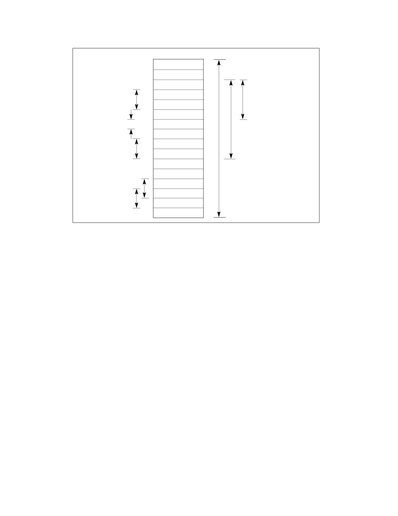
Figure 4-2 shows the byte order of each of the fundamental data types when referenced as operands in memory.
The low byte (bits 0 through 7) of each data type occupies the lowest address in memory and that address is also
the address of the operand.
Vol. 1
4-1
DATA TYPES
4EH
FH
12H
EH
7AH
DH
FEH
CH
Word at Address BH
Doubleword at Address AH
Contains FE06H
06H
BH
Contains 7AFE0636H
36H
AH
Byte at Address 9H
1FH
9H
Contains 1FH
Quadword at Address 6H
A4H
8H
Contains
7AFE06361FA4230BH
23H
7H
Word at Address 6H
Contains 230BH
0BH
6H
45H
5H
67H
4H
Word at Address 2H
74H
3H
Contains 74CBH
Double quadword at Address 0H
CBH
2H
Word at Address 1H
Contains
Contains CB31H
31H
1H
4E127AFE06361FA4230B456774CB311
12H
0H
Figure 4-2. Bytes, Words, Doublewords, Quadwords, and Double Quadwords in Memory
4.1.1
Alignment of Words, Doublewords, Quadwords, and Double Quadwords
Words, doublewords, and quadwords do not need to be aligned in memory on natural boundaries. The natural
boundaries for words, doublewords, and quadwords are even-numbered addresses, addresses evenly divisible by
four, and addresses evenly divisible by eight, respectively. However, to improve the performance of programs, data
structures (especially stacks) should be aligned on natural boundaries whenever possible. The reason for this is
that the processor requires two memory accesses to make an unaligned memory access; aligned accesses require
only one memory access. A word or doubleword operand that crosses a 4-byte boundary or a quadword operand
that crosses an 8-byte boundary is considered unaligned and requires two separate memory bus cycles for access.
Some instructions that operate on double quadwords require memory operands to be aligned on a natural
boundary. These instructions generate a general-protection exception (#GP) if an unaligned operand is specified. A
natural boundary for a double quadword is any address evenly divisible by 16. Other instructions that operate on
double quadwords permit unaligned access (without generating a general-protection exception). However, addi-
tional memory bus cycles are required to access unaligned data from memory.
4.2
NUMERIC DATA TYPES
Although bytes, words, and doublewords are fundamental data types, some instructions support additional inter-
pretations of these data types to allow operations to be performed on numeric data types (signed and unsigned
integers, and floating-point numbers). Single precision (32-bit) floating-point and double precision (64-bit)
floating-point data types are supported across all generations of Intel SSE extensions and Intel AVX extensions.
The half precision (16-bit) floating-point data type was supported only with F16C extensions (VCVTPH2PS and
VCVTPS2PH) beginning with the third generation of Intel® Core™ processors based on Ivy Bridge microarchitec-
ture. Starting with the 4th generation Intel® Xeon® Scalable Processor Family, an Intel® AVX-512 instruction set
architecture (ISA) for FP16 was added, supporting a wide range of general-purpose numeric operations for 16-bit
half precision floating-point values (binary16 in IEEE Standard 754-2019 for Floating-Point Arithmetic, aka half
precision or FP16), which complements the existing 32-bit and 64-bit floating-point instructions already available
in the Intel Xeon processor-based products. This ISA also provides complex-valued native hardware support for
half precision floating-point. See Figure 4-3.
4-2
Vol. 1

DATA TYPES
Byte Unsigned
Integer
7
0
Word Unsigned
Integer
15
0
Doubleword
Unsigned Integer
31
0
Quadword
Unsigned Integer
63
0
Sign
Byte Signed
Integer
Sign
7 6
0
Word Signed
Integer
1514
0
Sign
Doubleword Signed
Integer
Sign
31
30
0
Quadword Signed
Integer
63
62
0
Sign
Half Precision
Floating Point
Sign
15 14
9
0
Single Precision
Floating Point
Sign
31 30
23 22
0
Double Precision
Floating Point
63 62
52 51
0
Sign
Integer Bit
Double Extended
Precision Floating Point
79 78
64 63 62
0
SDM10024
Figure 4-3. Numeric Data Types
4.2.1
Integers
The Intel 64 and IA-32 architectures define two types of integers: unsigned and signed. Unsigned integers are ordi-
nary binary values ranging from 0 to the maximum positive number that can be encoded in the selected operand
size. Signed integers are two’s complement binary values that can be used to represent both positive and negative
integer values.
Some integer instructions (such as the ADD, SUB, PADDB, and PSUBB instructions) operate on either unsigned or
signed integer operands. Other integer instructions (such as IMUL, MUL, IDIV, DIV, FIADD, and FISUB) operate on
only one integer type.
The following sections describe the encodings and ranges of the two types of integers.
4.2.1.1
Unsigned Integers
Unsigned integers are unsigned binary numbers contained in a byte, word, doubleword, and quadword. Their
values range from 0 to 255 for an unsigned byte integer, from 0 to 65,535 for an unsigned word integer, from 0
Vol. 1
4-3

DATA TYPES
to 232 - 1 for an unsigned doubleword integer, and from 0 to 264 - 1 for an unsigned quadword integer. Unsigned
integers are sometimes referred to as ordinals.
4.2.1.2
Signed Integers
Signed integers are signed binary numbers held in a byte, word, doubleword, or quadword. All operations on signed
integers assume a two's complement representation. The sign bit is located in bit 7 in a byte integer, bit 15 in a
word integer, bit 31 in a doubleword integer, and bit 63 in a quadword integer (see the signed integer encodings in
Table 4-1).
Table 4-1. Signed Integer Encodings
Class
Two’s Complement Encoding
Sign
Positive
Largest
0
11..11
Smallest
0
00..01
Zero
0
00..00
Negative
Smallest
1
11..11
Largest
1
00..00
Integer indefinite
1
00..00
Signed Byte Integer:
← 7 bits →
Signed Word Integer:
← 15 bits →
Signed Doubleword Integer:
← 31 bits →
Signed Quadword Integer:
← 63 bits →
The sign bit is set for negative integers and cleared for positive integers and zero. Integer values range from -128
to +127 for a byte integer, from -32,768 to +32,767 for a word integer, from -231 to +231 - 1 for a doubleword
integer, and from -263 to +263 - 1 for a quadword integer.
When storing integer values in memory, word integers are stored in 2 consecutive bytes; doubleword integers are
stored in 4 consecutive bytes; and quadword integers are stored in 8 consecutive bytes.
The integer indefinite is a special value that is sometimes returned by the x87 FPU when operating on integer
values. For more information, see Section 8.2.1, “Indefinites.”
4.2.2
Floating-Point Data Types
The IA-32 architecture defines and operates on four floating-point data types: half precision floating-point, single
precision floating-point, double precision floating-point, and double-extended precision floating-point (see
Figure 4-3). The data formats for these data types correspond directly to formats specified in the IEEE Standard
754 for Floating-Point Arithmetic.
The half precision (16-bit) floating-point data type was supported only with F16C extensions (VCVTPH2PS and
VCVTPS2PH) beginning with the third generation of Intel Core processors based on Ivy Bridge microarchitecture.
Starting with the 4th generation Intel Xeon Scalable Processor Family, an Intel AVX-512 instruction set architecture
(ISA) for FP16 was added, supporting a wide range of general-purpose numeric operations for 16-bit half precision
floating-point values (binary16 in the IEEE Standard 754-2019 for Floating-Point Arithmetic, aka half precision or
FP16), which complements the existing 32-bit and 64-bit floating-point instructions already available in the Intel
Xeon processor-based products.
4-4
Vol. 1

DATA TYPES
Table 4-2 gives the length, precision, and approximate normalized range that can be represented by each of these
data types. Denormal values are also supported in each of these types.
Table 4-2. Length, Precision, and Range of Floating-Point Data Types
Data Type
Length
Precision
Approximate Normalized Range
(Bits)
(Bits)
Binary
Decimal
Half Precision
16
11
2-14 to 216
6.10 × 10⁻⁵ to 6.55 × 10⁴
Single Precision
32
24
2-126 to 2128
1.18 × 10-38 to 3.40 × 1038
Double Precision
64
53
2-1022 to 21024
2.23 × 10-308 to 1.80 × 10308
Double-Extended
80
64
2-16382 to 216384
3.36 × 10-4932 to 1.19 × 104932
Precision
NOTE
Section 4.8, “Real Numbers and Floating-Point Formats,” gives an overview of the IEEE Standard
754 floating-point formats and defines the terms integer bit, QNaN, SNaN, and denormal value.
Table 4-3 shows the floating-point encodings for zeros, denormalized finite numbers, normalized finite numbers,
infinites, and NaNs for each of the three floating-point data types. It also gives the format for the QNaN floating-
point indefinite value. (See Section 4.8.3.7, “QNaN Floating-Point Indefinite,” for a discussion of the use of the
QNaN floating-point indefinite value.)
For the half precision, single precision, and double precision formats, only the fraction part of the significand is
encoded. The integer is assumed to be 1 for all numbers except 0 and denormalized finite numbers. For the double
extended precision format, the integer is contained in bit 63, and the most-significant fraction bit is bit 62. Here,
the integer is explicitly set to 1 for normalized numbers, infinities, and NaNs, and to 0 for zero and denormalized
numbers.
Table 4-3. Floating-Point Number and NaN Encodings
Significand
Class
Sign
Biased Exponent
Integer1
Fraction
Positive
+∞
0
11..11
1
00..00
+Normals
0
11..10
1
11..11
0
00..01
1
00..00
+Denormals
0
00..00
0
11.11
0
00..00
0
00..01
+Zero
0
00..00
0
00..00
Negative
-Zero
1
00..00
0
00..00
−Denormals
1
00..00
0
00..01
1
00..00
0
11..11
−Normals
1
00..01
1
00..00
1
11..10
1
11..11
-∞
1
11..11
1
00..00
Vol. 1
4-5
DATA TYPES
Table 4-3. Floating-Point Number and NaN Encodings (Contd.)
Significand
Class
Sign
Biased Exponent
Integer1
Fraction
NaNs
SNaN
X
11..11
1
0X..XX2
QNaN
X
11..11
1
1X..XX
QNaN Floating-
1
11..11
1
10..00
Point Indefinite
Half Precision
← 5 Bits →
← 10 Bits →
← 8 Bits →
← 23 Bits →
Single Precision:
← 11 Bits →
← 52 Bits →
Double Precision:
← 15 Bits →
← 63 Bits →
Double Extended Precision:
NOTES:
1. Integer bit is implied and not stored for half precision, single precision, and double precision formats.
2. The fraction for SNaN encodings must be non-zero with the most-significant bit 0.
The exponent of each floating-point data type is encoded in biased format; see Section 4.8.2.2, “Biased Exponent.”
The biasing constant is 15 for the half precision format, 127 for the single precision format, 1023 for the double
precision format, and 16,383 for the double extended precision format.
When storing floating-point values in memory, half precision values are stored in 2 consecutive bytes in memory;
single precision values are stored in 4 consecutive bytes in memory; double precision values are stored in 8 consec-
utive bytes; and double extended precision values are stored in 10 consecutive bytes.
The single precision and double precision floating-point data types are operated on by x87 FPU, and Intel
SSE/SSE2/SSE3/SSE4.1/AVX instructions. The double extended precision floating-point format is only operated on
by the x87 FPU. See Section 11.6.8, “Compatibility of SIMD and x87 FPU Floating-Point Data Types,” for a discus-
sion of the compatibility of single precision and double precision floating-point data types between the x87 FPU and
Intel SSE/SSE2/SSE3 extensions.
4.2.3
Brain Float16
Brain Float16 (BF16 or bfloat16) is a shortened 16-bit version of the IEEE Standard 754 floating-point 32-bit
format. It aims to speed up training and inference for AI workloads. Figure 4-4 illustrates BF16 versus FP16 and
FP32.
FP32
s
8 bit exp
23 bit mantissa
FP16
s
5 bit exp
10 bit mantissa
BF16
s
8 bit exp
7 bit mantissa
BFP10001
Figure 4-4. Comparison of BF16 to FP16 and FP32
4.2.3.1
Numeric Definition
BF16 has one sign bit, eight exponent bits, and seven mantissa bits.
4-6
Vol. 1

DATA TYPES
Table 4-4. BF16 Format Numeric Definitions
Number
BF16 (E8M7)
Exponent Bias
127
Maximum Normal
S 11111110 11111111 = ± 2127 * 1.99 ~= ±3.39 * 1038
Minimum Normal
S 00000001 00000000 = ± 2-126 ~= ±1.18 * 10-38
Maximum Denormal
S 00000000 1111111 = ±2-126 * 0.99 ~= ±1.17 * 10-38
Minimum Denormal
S 00000000 0000001 = ±2-133 ~= ±9.18 * 10-41
NaNs
S 11111111 {non-zero}
Infinity
S 11111111 0000000
Zeros
S 00000000 0000000
Although denormal values are shown in the table, they are not used in computations (see Section 4.2.3.2).
4.2.3.2
Rounding, Denormal Handling, and FP Exceptions
Intel architecture supports BF16 in AMX dot product instructions, AVX dot product instructions, and AVX convert
instructions.
• Rounding: All operations are executed using Round to nearest (even) mode (e.g., for convert instructions).
• Denormal Handling: For BF16, input denormal values are replaced with zeros and FP32 underflow results are
flushed to zero. All instructions that accept BF16 inputs have FP32 results.
• Floating-point exceptions:
- Instructions operating on BF16 values neither consult nor update the MXCSR.
- Instructions operating on BF16 values do not raise exceptions.
4.3
POINTER DATA TYPES
Pointers are addresses of locations in memory.
In non-64-bit modes, the architecture defines two types of pointers: a near pointer and a far pointer. A near
pointer is a 32-bit (or 16-bit) offset (also called an effective address) within a segment. Near pointers are used
for all memory references in a flat memory model or for references in a segmented model where the identity of the
segment being accessed is implied.
A far pointer is a logical address, consisting of a 16-bit segment selector and a 32-bit (or 16-bit) offset. Far pointers
are used for memory references in a segmented memory model where the identity of a segment being accessed
must be specified explicitly. Near and far pointers with 32-bit offsets are shown in Figure 4-5.
Near Pointer
Offset
31
0
Far Pointer or Logical Address
Segment Selector
Offset
47
32 31
0
Figure 4-5. Pointer Data Types
Vol. 1
4-7
DATA TYPES
4.3.1
Pointer Data Types in 64-Bit Mode
In 64-bit mode (a sub-mode of IA-32e mode), a near pointer is 64 bits. This equates to an effective address. Far
pointers in 64-bit mode can be one of three forms:
•
16-bit segment selector, 16-bit offset if the operand size is 32 bits.
•
16-bit segment selector, 32-bit offset if the operand size is 32 bits.
•
16-bit segment selector, 64-bit offset if the operand size is 64 bits.
See Figure 4-6.
Near Pointer
64-bit Offset
63
0
Far Pointer with 64-bit Operand Size
16-bit Segment Selector
64-bit Offset
79
64 63
0
Far Pointer with 32-bit Operand Size
16-bit Segment Selector
32-bit Offset
47
32 31
0
Far Pointer with 32-bit Operand Size
16-bit Segment Selector
16-bit Offset
31
16 15
0
Figure 4-6. Pointers in 64-Bit Mode
4.4
BIT FIELD DATA TYPE
A bit field (see Figure 4-7) is a contiguous sequence of bits. It can begin at any bit position of any byte in memory
and can contain up to 32 bits.
Bit Field
Field Length
Least
Significant
Bit
Figure 4-7. Bit Field Data Type
4-8
Vol. 1
DATA TYPES
4.5
STRING DATA TYPES
Strings are continuous sequences of bits, bytes, words, or doublewords. A bit string can begin at any bit position
of any byte and can contain up to 232 - 1 bits. A byte string can contain bytes, words, or doublewords and can
range from zero to 232 - 1 bytes (4 GBytes).
4.6
PACKED SIMD DATA TYPES
Intel 64 and IA-32 architectures define and operate on a set of 64-bit and 128-bit packed data type for use in SIMD
operations. These data types consist of fundamental data types (packed bytes, words, doublewords, and quad-
words) and numeric interpretations of fundamental types for use in packed integer and packed floating-point oper-
ations.
4.6.1
64-Bit SIMD Packed Data Types
The 64-bit packed SIMD data types were introduced into the IA-32 architecture in the Intel MMX technology. They
are operated on in MMX registers. The fundamental 64-bit packed data types are packed bytes, packed words, and
packed doublewords (see Figure 4-8). When performing numeric SIMD operations on these data types, these data
types are interpreted as containing byte, word, or doubleword integer values.
Fundamental 64-Bit Packed SIMD Data Types
Packed Bytes
63
0
Packed Words
63
0
Packed Doublewords
63
0
64-Bit Packed Integer Data Types
Packed Byte Integers
63
0
Packed Word Integers
63
0
Packed Doubleword Integers
63
0
Figure 4-8. 64-Bit Packed SIMD Data Types
4.6.2
128-Bit Packed SIMD Data Types
The 128-bit packed SIMD data types were introduced into the IA-32 architecture in the Intel SSE extensions and
used with Intel SSE2, SSE3, SSSE3, SSE4.1, and AVX extensions. They are operated on primarily in the 128-bit
XMM registers and memory. The fundamental 128-bit packed data types are packed bytes, packed words, packed
doublewords, and packed quadwords (see Figure 4-9). When performing SIMD operations on these fundamental
data types in XMM registers, these data types are interpreted as containing packed or scalar half precision floating-
point, single precision floating-point or double precision floating-point values, or as containing packed byte, word,
doubleword, or quadword integer values.
Vol. 1
4-9

DATA TYPES
Fundamental 128-bit Packed SIMD Data Types
Packed Bytes
127
0
Packed Words
127
0
Packed Doublewords
127
0
Packed Quadwords
127
0
128-bit Packed Floating-Point and Integer Data Types
Packed Half Precision
Floating-Point
127
0
Packed Single Precision
Floating-Point
127
0
Packed Double Precision
Floating-Point
127
0
Packed Byte Integers
127
0
Packed Word Integers
127
0
Packed Doubleword
Integers
127
0
Packed Quadword
Integers
127
0
Figure 4-9. 128-Bit Packed SIMD Data Types
4.7
BCD AND PACKED BCD INTEGERS
Binary-coded decimal integers (BCD integers) are unsigned 4-bit integers with valid values ranging from 0 to 9. IA-
32 architecture defines operations on BCD integers located in one or more general-purpose registers or in one or
more x87 FPU registers (see Figure 4-10).
4-10
Vol. 1
DATA TYPES
BCD Integers
X
BCD
7
4
3
0
Packed BCD Integers
BCD BCD
7
43
0
80-Bit Packed BCD Decimal Integers
Sign
X
D17 D16 D15 D14 D13 D12 D11 D10 D9 D8 D7 D6
D5
D4
D3
D2
D1
D0
79
78
7271
0
4 Bits = 1 BCD Digit
Figure 4-10. BCD Data Types
When operating on BCD integers in general-purpose registers, the BCD values can be unpacked (one BCD digit per
byte) or packed (two BCD digits per byte). The value of an unpacked BCD integer is the binary value of the low half-
byte (bits 0 through 3). The high half-byte (bits 4 through 7) can be any value during addition and subtraction, but
must be zero during multiplication and division. Packed BCD integers allow two BCD digits to be contained in one
byte. Here, the digit in the high half-byte is more significant than the digit in the low half-byte.
When operating on BCD integers in x87 FPU data registers, BCD values are packed in an 80-bit format and referred
to as decimal integers. In this format, the first 9 bytes hold 18 BCD digits, 2 digits per byte. The least-significant
digit is contained in the lower half-byte of byte 0 and the most-significant digit is contained in the upper half-byte
of byte 9. The most significant bit of byte 10 contains the sign bit (0 = positive and 1 = negative; bits 0 through 6
of byte 10 are don’t care bits). Negative decimal integers are not stored in two's complement form; they are distin-
guished from positive decimal integers only by the sign bit. The range of decimal integers that can be encoded in
this format is -1018 + 1 to 1018 - 1.
The decimal integer format exists in memory only. When a decimal integer is loaded in an x87 FPU data register, it
is automatically converted to the double extended precision floating-point format. All decimal integers are exactly
representable in double extended precision format.
Table 4-5 gives the possible encodings of value in the decimal integer data type.
Table 4-5. Packed Decimal Integer Encodings
Magnitude
Class
Sign
digit
digit
digit
digit
digit
Positive
0
0000000
1001
1001
1001
1001
1001
Largest
Smallest
0
0000000
0000
0000
0000
0000
0001
Zero
0
0000000
0000
0000
0000
0000
0000
Negative
1
0000000
0000
0000
0000
0000
0000
Zero
Smallest
1
0000000
0000
0000
0000
0000
0001
Largest
1
0000000
1001
1001
1001
1001
1001
Vol. 1
4-11

DATA TYPES
Table 4-5. Packed Decimal Integer Encodings (Contd.)
Magnitude
Class
Sign
digit
digit
digit
digit
digit
Packed BCD
1
1111111
1111
1111
1100
0000
0000
Integer
Indefinite
← 1 byte →
← 9 bytes →
The packed BCD integer indefinite encoding (FFFFC000000000000000H) is stored by the FBSTP instruction in
response to a masked floating-point invalid-operation exception. Attempting to load this value with the FBLD
instruction produces an undefined result.
4.8
REAL NUMBERS AND FLOATING-POINT FORMATS
This section describes how real numbers are represented in floating-point format in x87 FPU and
SSE/SSE2/SSE3/SSE4.1 and Intel AVX floating-point instructions. It also introduces terms such as normalized
numbers, denormalized numbers, biased exponents, signed zeros, and NaNs. Readers who are already familiar
with floating-point processing techniques and the IEEE Standard 754 for Floating-Point Arithmetic may wish to skip
this section.
4.8.1
Real Number System
As shown in Figure 4-11, the real-number system comprises the continuum of real numbers from minus infinity (-
∞) to plus infinity (+ ∞).
Because the size and number of registers that any computer can have is limited, only a subset of the real-number
continuum can be used in real-number (floating-point) calculations. As shown at the bottom of Figure 4-11, the
subset of real numbers that the IA-32 architecture supports represents an approximation of the real number
system. The range and precision of this real-number subset is determined by the IEEE Standard 754 floating-point
formats.
4.8.2
Floating-Point Format
To increase the speed and efficiency of real-number computations, computers and microprocessors typically repre-
sent real numbers in a binary floating-point format. In this format, a real number has three parts: a sign, a signif-
icand, and an exponent (see Figure 4-12).
The sign is a binary value that indicates whether the number is positive (0) or negative (1). The significand has
two parts: a 1-bit binary integer (also referred to as the J-bit) and a binary fraction. The integer-bit is often not
represented, but instead is an implied value. The exponent is a binary integer that represents the base-2 power by
which the significand is multiplied.
Table 4-6 shows how the real number 178.125 (in ordinary decimal format) is stored in IEEE Standard 754 floating-
point format. The table lists a progression of real number notations that leads to the single precision, 32-bit
floating-point format. In this format, the significand is normalized (see Section 4.8.2.1, “Normalized Numbers”)
and the exponent is biased (see Section 4.8.2.2, “Biased Exponent”). For the single precision floating-point format,
the biasing constant is +127.
4-12
Vol. 1
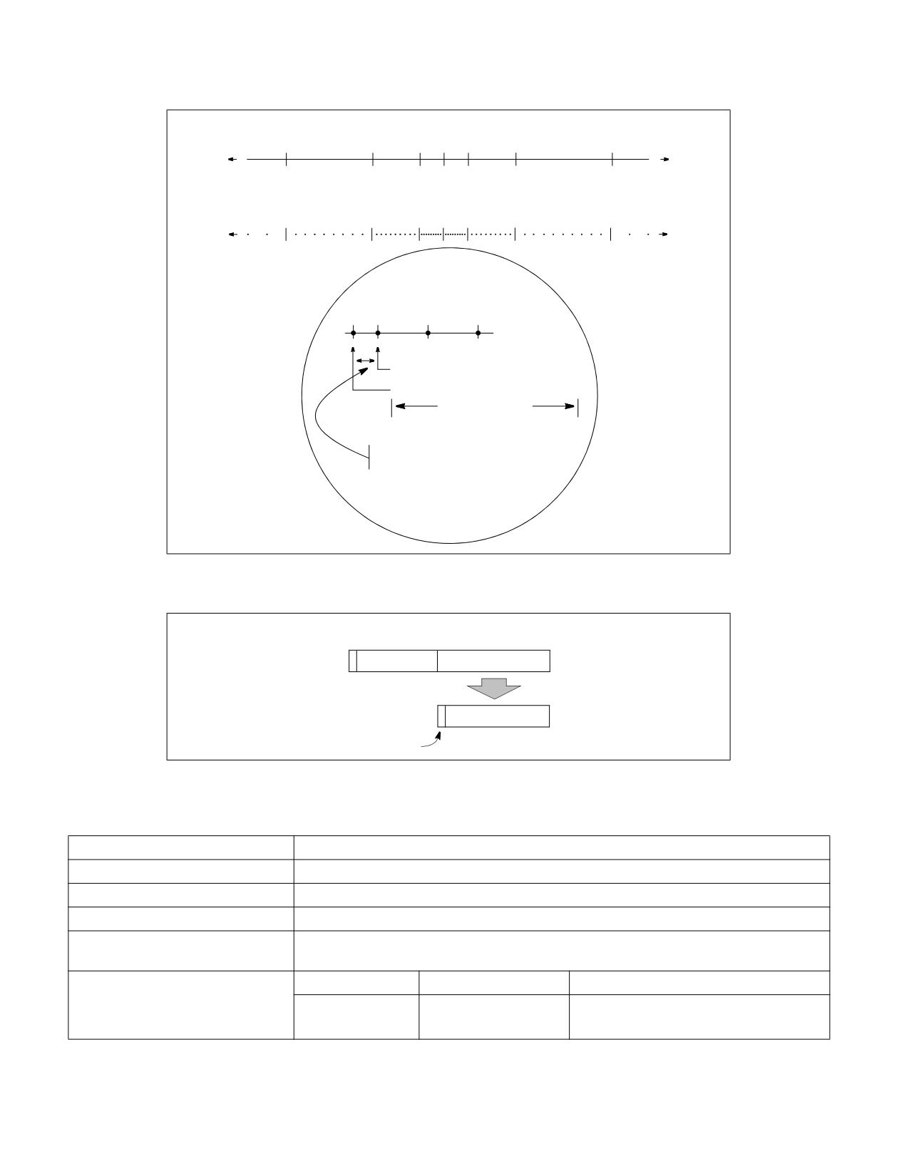
DATA TYPES
Binary Real Number System
-100
-10
-1
0
1
10
100
ςς
ςς
Subset of binary real numbers that can be represented with
IEEE single precision (32-bit) floating-point format
-100
-10
-1
0
1
10
100
ςς
ςς
+10
10.0000000000000000000000
1.11111111111111111111111
Precision
24 Binary Digits
Numbers within this range
cannot be represented.
Figure 4-11. Binary Real Number System
Sign
Exponent
Significand
Fraction
Integer or J-Bit
Figure 4-12. Binary Floating-Point Format
Table 4-6. Real and Floating-Point Number Notation
Notation
Value
Ordinary Decimal
178.125
Scientific Decimal
1.78125E10 2
Scientific Binary
1.0110010001E2111
Scientific Binary
1.0110010001E210000110
(Biased Exponent)
IEEE Single Precision Format
Sign
Biased Exponent
Normalized Significand
0
10000110
01100100010000000000000
1. (Implied)
Vol. 1
4-13
DATA TYPES
4.8.2.1
Normalized Numbers
In most cases, floating-point numbers are encoded in normalized form. This means that except for zero, the signif-
icand is always made up of an integer of 1 and the following fraction:
1.fff...ff
For values less than 1, leading zeros are eliminated. (For each leading zero eliminated, the exponent is decre-
mented by one.)
Representing numbers in normalized form maximizes the number of significant digits that can be accommodated
in a significand of a given width. To summarize, a normalized real number consists of a normalized significand that
represents a real number between 1 and 2 and an exponent that specifies the number’s binary point.
4.8.2.2
Biased Exponent
In the IA-32 architecture, the exponents of floating-point numbers are encoded in a biased form. This means that
a constant is added to the actual exponent so that the biased exponent is always a positive number. The value of
the biasing constant depends on the number of bits available for representing exponents in the floating-point
format being used. The biasing constant is chosen so that the smallest normalized number can be reciprocated
without overflow.
See Section 4.2.2, “Floating-Point Data Types,” for a list of the biasing constants that the IA-32 architecture uses
for the various sizes of floating-point data-types.
4.8.3
Real Number and Non-number Encodings
A variety of real numbers and special values can be encoded in the IEEE Standard 754 floating-point format. These
numbers and values are generally divided into the following classes:
• Signed zeros
• Denormalized finite numbers
• Normalized finite numbers
• Signed infinities
• NaNs
• Indefinite numbers
(The term NaN stands for “Not a Number.”)
Figure 4-13 shows how the encodings for these numbers and non-numbers fit into the real number continuum. The
encodings shown here are for the IEEE single precision floating-point format. The term “S” indicates the sign bit,
“E” the biased exponent, and “Sig” the significand. The exponent values are given in decimal. The integer bit is
shown for the significands, even though the integer bit is implied in single precision floating-point format.
4-14
Vol. 1
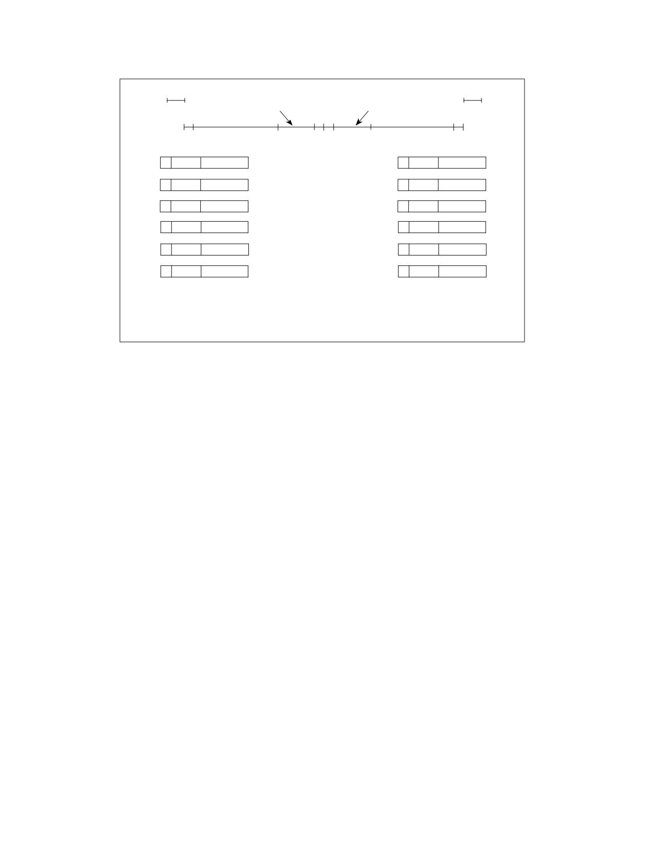
DATA TYPES
NaN
NaN
- Denormalized Finite
+ Denormalized Finite
- ∞ - Normalized Finite
-0+0
+ Normalized Finite
+∞
Real Number and NaN Encodings For 32-Bit Floating-Point Format
S
E
Sig1
S
E
Sig1
1
0
0.000...
-0
+0
0
0
0.000...
- Denormalized
+Denormalized
1
0
0.XXX...2
0
0
0.XXX...2
Finite
Finite
- Normalized
+Normalized
1
1...254
1.XXX...
0
1...254
1.XXX...
Finite
Finite
1
255
1.000...
-∞
+∞
0
255
1.000...
X3
255
1.0XX...2
SNaN
SNaN
X3
255
1.0XX...2
X3
255
1.1XX...
QNaN
QNaN
X3
255
1.1XX...
NOTES:
1. Integer bit of fraction implied for
single precision floating-point format.
2. Fraction must be non-zero.
3. Sign bit ignored.
Figure 4-13. Real Numbers and NaNs
An IA-32 processor can operate on and/or return any of these values, depending on the type of computation being
performed. The following sections describe these number and non-number classes.
4.8.3.1
Signed Zeros
Zero can be represented as a +0 or a -0 depending on the sign bit. Both encodings are equal in value. The sign of
a zero result depends on the operation being performed and the rounding mode being used. Signed zeros have
been provided to aid in implementing interval arithmetic. The sign of a zero may indicate the direction from which
underflow occurred, or it may indicate the sign of an ∞ that has been reciprocated.
4.8.3.2
Normalized and Denormalized Finite Numbers
Non-zero, finite numbers are divided into two classes: normalized and denormalized. The normalized finite
numbers comprise all the non-zero finite values that can be encoded in a normalized real number format between
zero and ∞. In the single precision floating-point format shown in Figure 4-13, this group of numbers includes all
the numbers with biased exponents ranging from 1 to 25410 (unbiased, the exponent range is from -12610 to
+12710).
When floating-point numbers become very close to zero, the normalized-number format can no longer be used to
represent the numbers. This is because the range of the exponent is not large enough to compensate for shifting
the binary point to the right to eliminate leading zeros.
When the biased exponent is zero, smaller numbers can only be represented by making the integer bit (and
perhaps other leading bits) of the significand zero. The numbers in this range are called denormalized numbers.
The use of leading zeros with denormalized numbers allows smaller numbers to be represented. However, this
denormalization may cause a loss of precision (the number of significant bits is reduced by the leading zeros).
When performing normalized floating-point computations, an IA-32 processor normally operates on normalized
numbers and produces normalized numbers as results. Denormalized numbers represent an underflow condition.
The exact conditions are specified in Section 4.9.1.5, “Numeric Underflow Exception (#U).”
A denormalized number is computed through a technique called gradual underflow. Table 4-7 gives an example of
gradual underflow in the denormalization process. Here the single precision format is being used, so the minimum
exponent (unbiased) is -12610. The true result in this example requires an exponent of -12910 in order to have a
Vol. 1
4-15

DATA TYPES
normalized number. Since -12910 is beyond the allowable exponent range, the result is denormalized by inserting
leading zeros until the minimum exponent of -12610 is reached.
Table 4-7. Denormalization Process
Operation
Sign
Exponent*
Significand
True Result
0
-129
1.01011100000...00
Denormalize
0
-128
0.10101110000...00
Denormalize
0
-127
0.01010111000...00
Denormalize
0
-126
0.00101011100...00
Denormal Result
0
-126
0.00101011100...00
* Expressed as an unbiased, decimal number.
In the extreme case, all the significant bits are shifted out to the right by leading zeros, creating a zero result.
The Intel 64 and IA-32 architectures deal with denormal values in the following ways:
• It avoids creating denormals by normalizing numbers whenever possible.
• It provides the floating-point underflow exception to permit programmers to detect cases when denormals are
created.
• It provides the floating-point denormal-operand exception to permit procedures or programs to detect when
denormals are being used as source operands for computations.
4.8.3.3
Signed Infinities
The two infinities, + ∞ and - ∞, represent the maximum positive and negative real numbers, respectively, that can
be represented in the floating-point format. Infinity is always represented by a significand of 1.00...00 (the integer
bit may be implied) and the maximum biased exponent allowed in the specified format (for example, 25510 for the
single precision format).
The signs of infinities are observed, and comparisons are possible. Infinities are always interpreted in the affine
sense; that is, -∞ is less than any finite number and +∞ is greater than any finite number. Arithmetic on infinities is
always exact. Exceptions are generated only when the use of an infinity as a source operand constitutes an invalid
operation.
Whereas denormalized numbers may represent an underflow condition, the two ∞ numbers may represent the
result of an overflow condition. Here, the normalized result of a computation has a biased exponent greater than
the largest allowable exponent for the selected result format.
4.8.3.4
NaNs
Since NaNs are non-numbers, they are not part of the real number line. In Figure 4-13, the encoding space for
NaNs in the floating-point formats is shown above the ends of the real number line. This space includes any value
with the maximum allowable biased exponent and a non-zero fraction (the sign bit is ignored for NaNs).
The IA-32 architecture defines two classes of NaNs: quiet NaNs (QNaNs) and signaling NaNs (SNaNs). A QNaN is a
NaN with the most significant fraction bit set; an SNaN is a NaN with the most significant fraction bit clear. QNaNs
are allowed to propagate through most arithmetic operations without signaling an exception. SNaNs generally
signal a floating-point invalid-operation exception whenever they appear as operands in arithmetic operations.
SNaNs are typically used to trap or invoke an exception handler. They must be inserted by software; that is, the
processor never generates an SNaN as a result of a floating-point operation.
4-16
Vol. 1

DATA TYPES
4.8.3.5
Operating on SNaNs and QNaNs
When a floating-point operation is performed on an SNaN and/or a QNaN, the result of the operation is either a
QNaN delivered to the destination operand or the generation of a floating-point invalid operation exception,
depending on the following rules:
• If one of the source operands is an SNaN and the floating-point invalid-operation exception is not masked (see
Section 4.9.1.1, “Invalid Operation Exception (#I)”), then a floating-point invalid-operation exception is
signaled and no result is stored in the destination operand. If one of the source operands is a QNaN and the
floating-point invalid-operation exception is not masked and the operation is one that generates an invalid-
operation exception for QNaN operands as described in Section 8.5.1.2, “Invalid Arithmetic Operand Exception
(#IA),” or Section 11.5.2.1, “Invalid Operation Exception (#I),” then a floating-point invalid-operation
exception is signaled and no result is stored in the destination operand.
• If either or both of the source operands are NaNs and floating-point invalid-operation exception is masked, the
result is as shown in Table 4-8. When an SNaN is converted to a QNaN, the conversion is handled by setting the
most-significant fraction bit of the SNaN to 1. Also, when one of the source operands is an SNaN, or when it is
a QNaN and the operation is one that generates an invalid-operation exception for QNaN operands as described
in Section 8.5.1.2, “Invalid Arithmetic Operand Exception (#IA),” or Section 11.5.2.1, “Invalid Operation
Exception (#I),” then the floating-point invalid-operation exception flag is set. Note that for some combinations
of source operands, the result is different for x87 FPU operations and for Intel SSE/SSE2/SSE3/SSE4.1
operations. Intel AVX follows the same behavior as Intel SSE/SSE2/SSE3/SSE4.1 in this respect.
• When neither of the source operands is a NaN, but the operation generates a floating-point invalid-operation
exception (see Tables 8-10 and 11-1), the result is commonly a QNaN FP Indefinite (Section 4.8.3.7).
Any exceptions to the behavior described in Table 4-8 are described in Section 8.5.1.2, “Invalid Arithmetic Operand
Exception (#IA),” and Section 11.5.2.1, “Invalid Operation Exception (#I).”
Table 4-8. Rules for Handling NaNs
Source Operands
Result1
SNaN and QNaN
X87 FPU - QNaN source operand.
SSE/SSE2/SSE3/SSE4.1/AVX - First source operand (if this operand is an
SNaN, it is converted to a QNaN).
Two SNaNs
X87 FPU - SNaN source operand with the larger significand, converted into a
QNaN.
SSE/SSE2/SSE3/SSE4.1/AVX - First source operand converted to a QNaN.
Two QNaNs
X87 FPU - QNaN source operand with the larger significand.
SSE/SSE2/SSE3/SSE4.1/AVX - First source operand.
SNaN and a floating-point value
SNaN source operand, converted into a QNaN.
QNaN and a floating-point value
QNaN source operand.
SNaN (for instructions that take only one operand)
SNaN source operand, converted into a QNaN.
QNaN (for instructions that take only one operand)
QNaN source operand.
NOTE:
1. For SSE/SSE2/SSE3/SSE4.1 instructions, the first operand is generally a source operand that becomes the destination operand. For
AVX instructions, the first source operand is usually the 2nd operand in a non-destructive source syntax. Within the Result column,
the x87 FPU notation also applies to the FISTTP instruction in SSE3; the SSE3 notation applies to the SIMD floating-point instruc-
tions.
4.8.3.6
Using SNaNs and QNaNs in Applications
Except for the rules given at the beginning of Section 4.8.3.4, “NaNs,” for encoding SNaNs and QNaNs, software is
free to use the bits in the significand of a NaN for any purpose. Both SNaNs and QNaNs can be encoded to carry and
store data, such as diagnostic information.
Vol. 1
4-17
DATA TYPES
By unmasking the invalid operation exception, the programmer can use signaling NaNs to trap to the exception
handler. The generality of this approach and the large number of NaN values that are available provide the sophis-
ticated programmer with a tool that can be applied to a variety of special situations.
For example, a compiler can use signaling NaNs as references to uninitialized (real) array elements. The compiler
can preinitialize each array element with a signaling NaN whose significand contains the index (relative position) of
the element. Then, if an application program attempts to access an element that it has not initialized, it can use the
NaN placed there by the compiler. If the invalid operation exception is unmasked, an interrupt will occur, and the
exception handler will be invoked. The exception handler can determine which element has been accessed, since
the operand address field of the exception pointer will point to the NaN, and the NaN will contain the index number
of the array element.
Quiet NaNs are often used to speed up debugging. In its early testing phase, a program often contains multiple
errors. An exception handler can be written to save diagnostic information in memory whenever it is invoked. After
storing the diagnostic data, it can supply a quiet NaN as the result of the erroneous instruction, and that NaN can
point to its associated diagnostic area in memory. The program will then continue, creating a different NaN for each
error. When the program ends, the NaN results can be used to access the diagnostic data saved at the time the
errors occurred. Many errors can thus be diagnosed and corrected in one test run.
In embedded applications that use computed results in further computations, an undetected QNaN can invalidate
all subsequent results. Such applications should therefore periodically check for QNaNs and provide a recovery
mechanism to be used if a QNaN result is detected.
4.8.3.7
QNaN Floating-Point Indefinite
For the floating-point data type encodings (single precision, double precision, and double extended precision), one
unique encoding (a QNaN) is reserved for representing the special value QNaN floating-point indefinite. The x87
FPU and the Intel SSE/SSE2/SSE3/SSE4.1/AVX extensions return these indefinite values as responses to some
masked floating-point exceptions. Table 4-3 shows the encoding used for the QNaN floating-point indefinite.
4.8.3.8
Half Precision Floating-Point Operation
Two instructions, VCVTPH2PS and VCVTPS2PH, which provide conversion only between half precision and single
precision floating-point values, were introduced with the F16C extensions beginning with the third generation of
Intel Core processors based on Ivy Bridge microarchitecture. Starting with the 4th generation Intel Xeon Scalable
Processor Family, an Intel AVX-512 instruction set architecture (ISA) for FP16 was added, supporting a wide range
of general-purpose numeric operations for 16-bit half precision floating-point values (binary16 in the IEEE Stan-
dard 754-2019 for Floating-Point Arithmetic, aka half precision or FP16). These additions complement the existing
32-bit and 64-bit floating-point instructions already available in the Intel Xeon processor-based products.
The SIMD floating-point exception behavior of the VCVTPH2PS and VCVTPS2PH instructions, as well as of the other
half precision instructions, are described in Section 14.4.1.
4.8.4
Rounding
When performing floating-point operations, the processor produces an infinitely precise floating-point result in the
destination format (half precision, single precision, double precision, or double extended precision floating-point)
whenever possible. However, because only a subset of the numbers in the real number continuum can be repre-
sented in IEEE Standard 754 floating-point formats, it is often the case that an infinitely precise result cannot be
encoded exactly in the format of the destination operand.
For example, the following value (a) has a 24-bit fraction. The least-significant bit of this fraction (the underlined
bit) cannot be encoded exactly in the single precision format (which has only a 23-bit fraction):
(a) 1.0001 0000 1000 0011 1001 0111E2 101
To round this result (a), the processor first selects two representable fractions b and c that most closely bracket a
in value (b < a < c).
(b) 1.0001 0000 1000 0011 1001 011E2 101
(c) 1.0001 0000 1000 0011 1001 100E2 101
4-18
Vol. 1

DATA TYPES
The processor then sets the result to b or to c according to the selected rounding mode. Rounding introduces an
error in a result that is less than one unit in the last place (the least significant bit position of the floating-point
value) to which the result is rounded.
The IEEE Standard 754 defines four rounding modes (see Table 4-9): round to nearest, round up, round down, and
round toward zero. The default rounding mode (for the Intel 64 and IA-32 architectures) is round to nearest. This
mode provides the most accurate and statistically unbiased estimate of the true result and is suitable for most
applications.
Table 4-9. Rounding Modes and Encoding of Rounding Control (RC) Field
Rounding Mode
RC Field
Description
Setting
Round to
00B
Rounded result is the closest to the infinitely precise result. If two values are equally close, the
nearest (even)
result is the even value (that is, the one with the least-significant bit of zero). Default
Round down
01B
Rounded result is closest to but no greater than the infinitely precise result.
(toward -∞)
Round up
10B
Rounded result is closest to but no less than the infinitely precise result.
(toward +∞)
Round toward
11B
Rounded result is closest to but no greater in absolute value than the infinitely precise result.
zero (Truncate)
The round up and round down modes are termed directed rounding and can be used to implement interval arith-
metic. Interval arithmetic is used to determine upper and lower bounds for the true result of a multistep computa-
tion, when the intermediate results of the computation are subject to rounding.
The round toward zero mode (sometimes called the “chop” mode) is commonly used when performing integer
arithmetic with the x87 FPU.
The rounded result is called the inexact result. When the processor produces an inexact result, the floating-point
precision (inexact) flag (PE) is set (see Section 4.9.1.6, “Inexact-Result (Precision) Exception (#P)”).
The rounding modes have no effect on comparison operations, operations that produce exact results, or operations
that produce NaN results.
4.8.4.1
Rounding Control (RC) Fields
In the Intel 64 and IA-32 architectures, the rounding mode is controlled by a 2-bit rounding-control (RC) field
(Table 4-9 shows the encoding of this field). The RC field is implemented in two different locations:
• X87 FPU control register (bits 10 and 11).
• The MXCSR register (bits 13 and 14).
Although these two RC fields perform the same function, they control rounding for different execution environ-
ments within the processor. The RC field in the x87 FPU control register controls rounding for computations
performed with the x87 FPU instructions; the RC field in the MXCSR register controls rounding for SIMD floating-
point computations performed with the Intel SSE/SSE2/SSE3/SSE4.1/AVX instructions.
4.8.4.2
Truncation with Intel® SSE, SSE2, and AVX Conversion Instructions
The following Intel SSE/SSE2 instructions automatically truncate the results of conversions from floating-point
values to integers when the result it inexact: CVTTPD2DQ, CVTTPS2DQ, CVTTPD2PI, CVTTPS2PI, CVTTSD2SI, and
CVTTSS2SI. Here, truncation means the round toward zero mode described in Table 4-9. There are also several
Intel AVX2 and AVX-512 instructions which use truncation (VCVTT*).
Vol. 1
4-19
DATA TYPES
4.9
OVERVIEW OF FLOATING-POINT EXCEPTIONS
The following section provides an overview of floating-point exceptions and their handling in the IA-32 architecture.
For information specific to the x87 FPU and to the Intel SSE/SSE2/SSE3/SSE4.1/AVX extensions, refer to the
following sections:
• Section 4.9, “Overview of Floating-Point Exceptions.”
• Section 11.5, “Intel® SSE, SSE2, and SSE3 Exceptions.”
• Section 12.8.4, “IEEE 754 Compliance of Intel® SSE4.1 Floating-Point Instructions.”
• Section 14.10, “SIMD Floating-Point Exceptions.”
When operating on floating-point operands, the IA-32 architecture recognizes and detects six classes of exception
conditions:
• Invalid operation (#I).
• Divide-by-zero (#Z).
• Denormalized operand (#D).
• Numeric overflow (#O).
• Numeric underflow (#U).
• Inexact result (precision) (#P).
The nomenclature of “#” symbol followed by one or two letters (for example, #P) is used in this manual to indicate
exception conditions. It is merely a short-hand form and is not related to assembler mnemonics.
NOTE
All of the exceptions listed above except the denormal-operand exception (#D) are defined in IEEE
Standard 754.
The invalid-operation, divide-by-zero and denormal-operand exceptions are pre-computation exceptions (that is,
they are detected before any arithmetic operation occurs). The numeric-underflow, numeric-overflow and precision
exceptions are post-computation exceptions.
Each of the six exception classes has a corresponding flag bit (IE, ZE, OE, UE, DE, or PE) and mask bit (IM, ZM, OM,
UM, DM, or PM). When one or more floating-point exception conditions are detected, the processor sets the appro-
priate flag bits, then takes one of two possible courses of action, depending on the settings of the corresponding
mask bits:
• Mask bit set. Handles the exception automatically, producing a predefined (and often times usable) result,
while allowing program execution to continue undisturbed.
• Mask bit clear. Invokes a software exception handler to handle the exception.
The masked (default) responses to exceptions have been chosen to deliver a reasonable result for each exception
condition and are generally satisfactory for most floating-point applications. By masking or unmasking specific
floating-point exceptions, programmers can delegate responsibility for most exceptions to the processor and
reserve the most severe exception conditions for software exception handlers.
Because the exception flags are “sticky,” they provide a cumulative record of the exceptions that have occurred
since they were last cleared. A programmer can thus mask all exceptions, run a calculation, and then inspect the
exception flags to see if any exceptions were detected during the calculation.
In the IA-32 architecture, floating-point exception flag and mask bits are implemented in two different locations:
• X87 FPU status word and control word. The flag bits are located at bits 0 through 5 of the x87 FPU status word
and the mask bits are located at bits 0 through 5 of the x87 FPU control word (see Figures 8-4 and 8-6).
• MXCSR register. The flag bits are located at bits 0 through 5 of the MXCSR register and the mask bits are
located at bits 7 through 12 of the register (see Figure 10-3).
Although these two sets of flag and mask bits perform the same function, they report on and control exceptions for
different execution environments within the processor. The flag and mask bits in the x87 FPU status and control
words control exception reporting and masking for computations performed with the x87 FPU instructions; the
4-20
Vol. 1
DATA TYPES
companion bits in the MXCSR register control exception reporting and masking for SIMD floating-point computa-
tions performed with the Intel SSE/SSE2/SSE3/SSE4.1/AVX instructions.
Note that when exceptions are masked, the processor may detect multiple exceptions in a single instruction,
because it continues executing the instruction after performing its masked response. For example, the processor
can detect a denormalized operand, perform its masked response to this exception, and then detect numeric
underflow.
See Section 4.9.2, “Floating-Point Exception Priority,” for a description of the rules for exception precedence when
more than one floating-point exception condition is detected for an instruction.
4.9.1
Floating-Point Exception Conditions
The following sections describe the various conditions that cause a floating-point exception to be generated and the
masked response of the processor when these conditions are detected. The Intel® 64 and IA-32 Architectures Soft-
ware Developer’s Manual, Volumes 3A, 3B, 3C, & 3D, lists the floating-point exceptions that can be signaled for
each floating-point instruction.
4.9.1.1
Invalid Operation Exception (#I)
The processor reports an invalid operation exception in response to one or more invalid arithmetic operands. If the
invalid operation exception is masked, the processor sets the IE flag and returns an indefinite value or a QNaN. This
value overwrites the destination register specified by the instruction. If the invalid operation exception is not
masked, the IE flag is set, a software exception handler is invoked, and the operands remain unaltered.
See Section 4.8.3.6, “Using SNaNs and QNaNs in Applications,” for information about the result returned when an
exception is caused by an SNaN.
The processor can detect a variety of invalid arithmetic operations that can be coded in a program. These opera-
tions generally indicate a programming error, such as dividing ∞ by ∞ . See the following sections for information
regarding the invalid-operation exception when detected while executing x87 FPU or Intel
SSE/SSE2/SSE3/SSE4.1/AVX instructions:
• X87 FPU; Section 8.5.1, “Invalid Operation Exception.”
• SIMD floating-point exceptions; Section 11.5.2.1, “Invalid Operation Exception (#I).”
• Section 12.8.4, “IEEE 754 Compliance of Intel® SSE4.1 Floating-Point Instructions.”
• Section 14.10, “SIMD Floating-Point Exceptions.”
4.9.1.2
Denormal Operand Exception (#D)
The processor reports the denormal-operand exception if an arithmetic instruction attempts to operate on a
denormal operand (see Section 4.8.3.2, “Normalized and Denormalized Finite Numbers”). When the exception is
masked, the processor sets the DE flag and proceeds with the instruction. Operating on denormal numbers will
produce results at least as good as, and often better than, what can be obtained when denormal numbers are
flushed to zero. Programmers can mask this exception so that a computation may proceed, then analyze any loss
of accuracy when the final result is delivered.
When a denormal-operand exception is not masked, the DE flag is set, a software exception handler is invoked, and
the operands remain unaltered. When denormal operands have reduced significance due to loss of low-order bits,
it may be advisable to not operate on them. Precluding denormal operands from computations can be accom-
plished by an exception handler that responds to unmasked denormal-operand exceptions.
See the following sections for information regarding the denormal-operand exception when detected while
executing x87 FPU or Intel SSE/SSE2/SSE3/SSE4.1/AVX instructions:
• X87 FPU; Section 8.5.2, “Denormal Operand Exception (#D).”
• SIMD floating-point exceptions; Section 11.5.2.2, “Denormal-Operand Exception (#D).”
• Section 12.8.4, “IEEE 754 Compliance of Intel® SSE4.1 Floating-Point Instructions.”
• Section 14.10, “SIMD Floating-Point Exceptions.”
Vol. 1
4-21

DATA TYPES
4.9.1.3
Divide-By-Zero Exception (#Z)
The processor reports the floating-point divide-by-zero exception whenever an instruction attempts to divide a
finite non-zero operand by 0. The masked response for the divide-by-zero exception is to set the ZE flag and return
an infinity signed with the exclusive OR of the sign of the operands. If the divide-by-zero exception is not masked,
the ZE flag is set, a software exception handler is invoked, and the operands remain unaltered.
See the following sections for information regarding the divide-by-zero exception when detected while executing
x87 FPU or Intel SSE/SSE2/AVX instructions:
• X87 FPU; Section 8.5.3, “Divide-By-Zero Exception (#Z).”
• SIMD floating-point exceptions; Section 11.5.2.3, “Divide-By-Zero Exception (#Z).”
• Section 12.8.4, “IEEE 754 Compliance of Intel® SSE4.1 Floating-Point Instructions.”
• Section 14.10, “SIMD Floating-Point Exceptions.”
4.9.1.4
Numeric Overflow Exception (#O)
The processor reports a floating-point numeric overflow exception whenever the rounded result of an instruction
exceeds the largest allowable finite value that will fit into the destination operand. Table 4-10 shows the threshold
range for numeric overflow for each of the floating-point formats; overflow occurs when a rounded result falls at or
outside this threshold range.
Table 4-10. Numeric Overflow Thresholds
Floating-Point Format
Overflow Thresholds
Half Precision
| x | ≥ 1.0 ∗ 216
Single Precision
| x | ≥ 1.0 ∗ 2128
Double Precision
| x | ≥ 1.0 ∗ 21024
Double Extended Precision
| x | ≥ 1.0 ∗ 216384
When a numeric-overflow exception occurs and the exception is masked, the processor sets the OE flag and returns
one of the values shown in Table 4-11, according to the current rounding mode. See Section 4.8.4, “Rounding.”
When numeric overflow occurs and the numeric-overflow exception is not masked, the OE flag is set, a software
exception handler is invoked, and the source and destination operands either remain unchanged or a biased result
is stored in the destination operand (depending whether the overflow exception was generated during an Intel
SSE/SSE2/SSE3/SSE4.1/AVX floating-point operation or an x87 FPU operation).
Table 4-11. Masked Responses to Numeric Overflow
Rounding Mode
Sign of True Result
Result
To nearest
+
+∞
–
-∞
Toward -∞
+
Largest finite positive number
–
-∞
Toward +∞
+
+∞
–
Largest finite negative number
Toward zero
+
Largest finite positive number
-
Largest finite negative number
See the following sections for information regarding the numeric overflow exception when detected while executing
x87 FPU instructions or while executing Intel SSE/SSE2/SSE3/SSE4.1/AVX instructions:
• X87 FPU; Section 8.5.4, “Numeric Overflow Exception (#O).”
• SIMD floating-point exceptions; Section 11.5.2.4, “Numeric Overflow Exception (#O).”
4-22
Vol. 1
DATA TYPES
• Section 12.8.4, “IEEE 754 Compliance of Intel® SSE4.1 Floating-Point Instructions.”
• Section 14.10, “SIMD Floating-Point Exceptions.”
4.9.1.5
Numeric Underflow Exception (#U)
The processor detects a potential floating-point numeric underflow condition whenever the result of rounding with
unbounded exponent (taking into account precision control for x87) is non-zero and tiny; that is, non-zero and less
than the smallest possible normalized, finite value that will fit into the destination operand. Table 4-12 shows the
threshold range for numeric underflow for each of the floating-point formats (assuming normalized results);
underflow occurs when a rounded result falls strictly within the threshold range. The ability to detect and handle
underflow is provided to prevent a very small result from propagating through a computation and causing another
exception (such as overflow during division) to be generated at a later time. Results which trigger underflow are
also potentially less accurate.
Table 4-12. Numeric Underflow (Normalized) Thresholds
Floating-Point Format
Underflow Thresholds1
Half Precision
| x | < 1.0 ∗ 2-14
Single Precision
| x | < 1.0 ∗ 2-126
Double Precision
| x | < 1.0 ∗ 2-1022
Double Extended Precision
| x | < 1.0 ∗ 2-16382
NOTES:
1. Where ‘x’ is the result rounded to destination precision with an unbounded exponent range.
How the processor handles an underflow condition, depends on two related conditions:
• Creation of a tiny, non-zero result.
• Creation of an inexact result; that is, a result that cannot be represented exactly in the destination format.
Which of these events causes an underflow exception to be reported and how the processor responds to the excep-
tion condition depends on whether the underflow exception is masked:
• Underflow exception masked - The underflow exception is reported (the UE flag is set) only when the
result is both tiny and inexact. The processor returns a correctly signed result whose magnitude is less than or
equal to the smallest positive normal floating-point number to the destination operand, regardless of
inexactness.
• Underflow exception not masked - The underflow exception is reported when the result is non-zero tiny,
regardless of inexactness. The processor leaves the source and destination operands unaltered or stores a
biased result in the destination operand (depending whether the underflow exception was generated during an
Intel SSE/SSE2/SSE3/AVX floating-point operation or an x87 FPU operation) and invokes a software exception
handler.
See the following sections for information regarding the numeric underflow exception when detected while
executing x87 FPU instructions or while executing Intel SSE/SSE2/SSE3/SSE4.1/AVX instructions:
• X87 FPU; Section 8.5.5, “Numeric Underflow Exception (#U).”
• SIMD floating-point exceptions; Section 11.5.2.5, “Numeric Underflow Exception (#U).”
• Section 12.8.4, “IEEE 754 Compliance of Intel® SSE4.1 Floating-Point Instructions.”
• Section 14.10, “SIMD Floating-Point Exceptions.”
4.9.1.6
Inexact-Result (Precision) Exception (#P)
The inexact-result exception (also called the precision exception) occurs if the result of an operation is not exactly
representable in the destination format. For example, the fraction 1/3 cannot be precisely represented in binary
floating-point form. This exception occurs frequently and indicates that some (normally acceptable) accuracy will
be lost due to rounding. The exception is supported for applications that need to perform exact arithmetic only.
Because the rounded result is generally satisfactory for most applications, this exception is commonly masked.
Vol. 1
4-23
DATA TYPES
If the inexact-result exception is masked when an inexact-result condition occurs and a numeric overflow or under-
flow condition has not occurred, the processor sets the PE flag and stores the rounded result in the destination
operand. The current rounding mode determines the method used to round the result. See Section 4.8.4,
“Rounding.”
If the inexact-result exception is not masked when an inexact result occurs and numeric overflow or underflow has
not occurred, the PE flag is set, the rounded result is stored in the destination operand, and a software exception
handler is invoked.
If an inexact result occurs in conjunction with numeric overflow or underflow, one of the following operations is
carried out:
• If an inexact result occurs along with masked overflow or underflow, the OE flag or UE flag and the PE flag are
set and the result is stored as described for the overflow or underflow exceptions; see Section 4.9.1.4,
“Numeric Overflow Exception (#O),” or Section 4.9.1.5, “Numeric Underflow Exception (#U).” If the inexact
result exception is unmasked, the processor also invokes a software exception handler.
• If an inexact result occurs along with unmasked overflow or underflow and the destination operand is a register,
the OE or UE flag and the PE flag are set, the result is stored as described for the overflow or underflow
exceptions, and a software exception handler is invoked.
If an unmasked numeric overflow or underflow exception occurs and the destination operand is a memory location
(which can happen only for a floating-point store), the inexact-result condition is not reported and the C1 flag is
cleared.
See the following sections for information regarding the inexact-result exception when detected while executing
x87 FPU or Intel SSE/SSE2/SSE3/SSE4.1/AVX instructions:
• X87 FPU; Section 8.5.6, “Inexact-Result (Precision) Exception (#P).”
• SIMD floating-point exceptions; Section 11.5.2.3, “Divide-By-Zero Exception (#Z).”
• Section 12.8.4, “IEEE 754 Compliance of Intel® SSE4.1 Floating-Point Instructions.”
• Section 14.10, “SIMD Floating-Point Exceptions.”
4.9.2
Floating-Point Exception Priority
The processor handles exceptions according to a predetermined precedence. When an instruction generates two or
more exception conditions, the exception precedence sometimes results in the higher-priority exception being
handled and the lower-priority exceptions being ignored. For example, dividing an SNaN by zero can potentially
signal an invalid-operation exception (due to the SNaN operand) and a divide-by-zero exception. Here, if both
exceptions are masked, the processor handles the higher-priority exception only (the invalid-operation exception),
returning a QNaN to the destination. Alternately, a denormal-operand or inexact-result exception can accompany a
numeric underflow or overflow exception with both exceptions being handled.
The precedence for floating-point exceptions is as follows:
1. Invalid-operation exception, subdivided as follows:
a. Stack underflow (occurs with x87 FPU only).
b. Stack overflow (occurs with x87 FPU only).
c. Operand of unsupported format (occurs with x87 FPU only when using the double extended precision
floating-point format).
d. SNaN operand.
2. QNaN operand. Though this is not an exception, the handling of a QNaN operand has precedence over lower-
priority exceptions. For example, a QNaN divided by zero results in a QNaN, not a zero-divide exception.
3. Any other invalid-operation exception not mentioned above or a divide-by-zero exception.
4. Denormal-operand exception. If masked, then instruction execution continues, and a lower-priority exception
can occur as well.
5. Numeric overflow and underflow exceptions; possibly in conjunction with the inexact-result exception.
6. Inexact-result exception.
4-24
Vol. 1
DATA TYPES
Invalid operation, zero divide, and denormal operand exceptions are detected before a floating-point operation
begins. Overflow, underflow, and precision exceptions are not detected until a true result has been computed.
When an unmasked pre-operation exception is detected, the destination operand has not yet been updated, and
appears as if the offending instruction has not been executed. When an unmasked post-operation exception is
detected, the destination operand may be updated with a result, depending on the nature of the exception (except
for Intel SSE/SSE2/SSE3/AVX instructions, which do not update their destination operands in such cases).
4.9.3
Typical Actions of a Floating-Point Exception Handler
After the floating-point exception handler is invoked, the processor handles the exception in the same manner that
it handles non-floating-point exceptions. The floating-point exception handler is normally part of the operating
system or executive software, and it usually invokes a user-registered floating-point exception handle.
A typical action of the exception handler is to store state information in memory. Other typical exception handler
actions include:
• Examining the stored state information to determine the nature of the error.
• Taking actions to correct the condition that caused the error.
• Clearing the exception flags.
• Returning to the interrupted program and resuming normal execution.
In lieu of writing recovery procedures, the exception handler can do the following:
• Increment in software an exception counter for later display or printing.
• Print or display diagnostic information (such as the state information).
• Halt further program execution.
Vol. 1
4-25
DATA TYPES
4-26
Vol. 1
CHAPTER 5
INSTRUCTION SET SUMMARY
This chapter provides an abridged overview of Intel 64 and IA-32 instructions. Instructions are divided into the
following groups:
•
Section 5.1, “General-Purpose Instructions.”
•
Section 5.2, “x87 FPU Instructions.”
•
Section 5.3, “x87 FPU AND SIMD State Management Instructions.”
•
Section 5.4, “MMX Instructions.”
•
Section 5.5, “Intel® SSE Instructions.”
•
Section 5.6, “Intel® SSE2 Instructions.”
•
Section 5.7, “Intel® SSE3 Instructions.”
•
Section 5.8, “Supplemental Streaming SIMD Extensions 3 (SSSE3) Instructions.”
•
Section 5.9, “Intel® SSE4 Instructions.”
•
Section 5.10, “Intel® SSE4.1 Instructions.”
•
Section 5.11, “Intel® SSE4.2 Instruction Set.”
•
Section 5.12, “Intel® AES-NI and PCLMULQDQ.”
•
Section 5.13, “Intel® Advanced Vector Extensions (Intel® AVX).”
•
Section 5.14, “16-bit Floating-Point Conversion.”
•
Section 5.15, “Fused-Multiply-ADD (FMA).”
•
Section 5.16, “Intel® Advanced Vector Extensions 2 (Intel® AVX2).”
•
Section 5.17, “Intel® Transactional Synchronization Extensions (Intel® TSX).”
•
Section 5.18, “Intel® SHA Extensions.”
•
Section 5.19, “Intel® Advanced Vector Extensions 512 (Intel® AVX-512).”
•
Section 5.20, “System Instructions.”
•
Section 5.21, “64-Bit Mode Instructions.”
•
Section 5.22, “Virtual-Machine Extensions.”
•
Section 5.23, “Safer Mode Extensions.”
•
Section 5.24, “Intel® Memory Protection Extensions.”
•
Section 5.25, “Intel® Software Guard Extensions.”
•
Section 5.26, “Shadow Stack Management Instructions.”
•
Section 5.27, “Control Transfer Terminating Instructions.”
•
Section 5.28, “Intel® AMX Instructions.”
•
Section 5.29, “User Interrupt Instructions.”
•
Section 5.30, “Enqueue Store Instructions.”
•
Section 5.31, “Intel® Advanced Vector Extensions 10 Version 1 Instructions.”
Table 5-1 lists the groups and IA-32 processors that support each group. More recent instruction set extensions are
listed in Table 5-2. Within these groups, most instructions are collected into functional subgroups.
Vol. 1
5-1
INSTRUCTION SET SUMMARY
Table 5-1. Instruction Groups in Intel® 64 and IA-32 Processors
Instruction Set
Architecture
Intel 64 and IA-32 Processor Support
General Purpose
All Intel 64 and IA-32 processors.
X87 FPU
Intel486, Pentium, Pentium with MMX Technology, Celeron, Pentium Pro, Pentium II, Pentium II Xeon,
Pentium III, Pentium III Xeon, Pentium 4, Intel Xeon processors, Pentium M, Intel Core Solo, Intel Core Duo,
Intel Core 2 Duo processors, Intel Atom processors.
X87 FPU and SIMD State
Pentium II, Pentium II Xeon, Pentium III, Pentium III Xeon, Pentium 4, Intel Xeon processors, Pentium M,
Management
Intel Core Solo, Intel Core Duo, Intel Core 2 Duo processors, Intel Atom processors.
MMX Technology
Pentium with MMX Technology, Celeron, Pentium II, Pentium II Xeon, Pentium III, Pentium III Xeon, Pentium
4, Intel Xeon processors, Pentium M, Intel Core Solo, Intel Core Duo, Intel Core 2 Duo processors, Intel Atom
processors.
SSE Extensions
Pentium III, Pentium III Xeon, Pentium 4, Intel Xeon processors, Pentium M, Intel Core Solo, Intel Core Duo,
Intel Core 2 Duo processors, Intel Atom processors.
SSE2 Extensions
Pentium 4, Intel Xeon processors, Pentium M, Intel Core Solo, Intel Core Duo, Intel Core 2 Duo processors,
Intel Atom processors.
SSE3 Extensions
Pentium 4 supporting HT Technology (built on 90 nm process technology), Intel Core Solo, Intel Core Duo,
Intel Core 2 Duo processors, Intel Xeon processor 3xxxx, 5xxx, 7xxx Series, Intel Atom processors.
SSSE3 Extensions
Intel Xeon processor 3xxx, 5100, 5200, 5300, 5400, 5500, 5600, 7300, 7400, 7500 series, Intel Core 2
Extreme processors QX6000 series, Intel Core 2 Duo, Intel Core 2 Quad processors, Intel Pentium Dual-Core
processors, Intel Atom processors.
IA-32e mode: 64-bit
Intel 64 processors.
mode instructions
System Instructions
Intel 64 and IA-32 processors.
VMX Instructions
Intel 64 and IA-32 processors supporting Intel Virtualization Technology.
SMX Instructions
Intel Core 2 Duo processor E6x50, E8xxx; Intel Core 2 Quad processor Q9xxx.
Table 5-2. Instruction Set Extensions Introduction in Intel® 64 and IA-32 Processors
Instruction Set Architecture
Processor Generation Introduction
SSE4.1 Extensions
Intel® Xeon® processor 3100, 3300, 5200, 5400, 7400, 7500 series, Intel® Core™ 2 Extreme
processors QX9000 series, Intel® Core™ 2 Quad processor Q9000 series, Intel® Core™ 2 Duo processors
8000 series and T9000 series, Intel Atom® processor based on Silvermont microarchitecture.
SSE4.2 Extensions, CRC32,
Intel® Core™ i7 965 processor, Intel® Xeon® processors X3400, X3500, X5500, X6500, X7500 series,
POPCNT
Intel Atom processor based on Silvermont microarchitecture.
Intel® AES-NI, PCLMULQDQ
Intel® Xeon® processor E7 series, Intel® Xeon® processors X3600 and X5600, Intel® Core™ i7 980X
processor, Intel Atom processor based on Silvermont microarchitecture. Use CPUID to verify presence
of Intel AES-NI and PCLMULQDQ across Intel® Core™ processor families.
Intel® AVX
Intel® Xeon® processor E3 and E5 families, 2nd Generation Intel® Core™ i7, i5, i3 processor 2xxx
families.
F16C
3rd Generation Intel® Core™ processors, Intel® Xeon® processor E3-1200 v2 product family, Intel®
Xeon® processor E5 v2 and E7 v2 families.
RDRAND
3rd Generation Intel Core processors, Intel Xeon processor E3-1200 v2 product family, Intel Xeon
processor E5 v2 and E7 v2 families, Intel Atom processor based on Silvermont microarchitecture.
FS/GS base access
3rd Generation Intel Core processors, Intel Xeon processor E3-1200 v2 product family, Intel Xeon
processor E5 v2 and E7 v2 families, Intel Atom® processor based on Goldmont microarchitecture.
5-2
Vol. 1
INSTRUCTION SET SUMMARY
Table 5-2. Instruction Set Extensions Introduction in Intel® 64 and IA-32 Processors (Contd.)
Instruction Set Architecture
Processor Generation Introduction
FMA, AVX2, BMI1, BMI2,
Intel® Xeon® processor E3/E5/E7 v3 product families, 4th Generation Intel® Core™ processor family.
INVPCID, LZCNT, Intel® TSX
MOVBE
Intel Xeon processor E3/E5/E7 v3 product families, 4th Generation Intel Core processor family, Intel
Atom processors.
PREFETCHW
Intel® Core™ M processor family; 5th Generation Intel® Core™ processor family, Intel Atom processor
based on Silvermont microarchitecture.
ADX
Intel Core M processor family, 5th Generation Intel Core processor family.
RDSEED, CLAC, STAC
Intel Core M processor family, 5th Generation Intel Core processor family, Intel Atom processor based
on Goldmont microarchitecture.
AVX512ER, AVX512PF,
Intel® Xeon Phi™ Processor 3200, 5200, 7200 Series.
PREFETCHWT1
AVX512F, AVX512CD
Intel Xeon Phi Processor 3200, 5200, 7200 Series, Intel® Xeon® Scalable Processor Family, Intel® Core™
i3-8121U processor.
CLFLUSHOPT, XSAVEC,
Intel Xeon Scalable Processor Family, 6th Generation Intel® Core™ processor family, Intel Atom
XSAVES, Intel® MPX
processor based on Goldmont microarchitecture.
SGX1
6th Generation Intel Core processor family, Intel Atom® processor based on Goldmont Plus
microarchitecture.
AVX512DQ, AVX512BW,
Intel Xeon Scalable Processor Family, Intel Core i3-8121U processor based on Cannon Lake
AVX512VL
microarchitecture.
CLWB
Intel Xeon Scalable Processor Family, Intel Atom® processor based on Tremont microarchitecture, 11th
Generation Intel Core processor family based on Tiger Lake microarchitecture.
PKU
Intel Xeon Scalable Processor Family, 10th generation Intel® Core™ processors based on Comet Lake
microarchitecture.
AVX512_IFMA,
Intel Core i3-8121U processor based on Cannon Lake microarchitecture.
AVX512_VBMI
Intel® SHA Extensions
Intel Core i3-8121U processor based on Cannon Lake microarchitecture, Intel Atom processor based
on Goldmont microarchitecture, 3rd Generation Intel® Xeon® Scalable Processor Family based on Ice
Lake microarchitecture.
UMIP
Intel Core i3-8121U processor based on Cannon Lake microarchitecture, Intel Atom processor based
on Goldmont Plus microarchitecture.
PTWRITE
Intel Atom processor based on Goldmont Plus microarchitecture, 12th generation Intel® Core™
processor supporting Alder Lake performance hybrid architecture, 4th generation Intel® Xeon®
Scalable Processor Family based on Sapphire Rapids microarchitecture.
RDPID
10th Generation Intel® Core™ processor family based on Ice Lake microarchitecture, Intel Atom
processor based on Goldmont Plus microarchitecture.
AVX512_4FMAPS,
Intel® Xeon Phi™ Processor 7215, 7285, 7295 Series.
AVX512_4VNNIW
AVX512_VNNI
2nd Generation Intel® Xeon® Scalable Processor Family, 10th Generation Intel Core processor family
based on Ice Lake microarchitecture.
AVX512_VPOPCNTDQ
Intel Xeon Phi Processor 7215, 7285, 7295 Series, 10th Generation Intel Core processor family based
on Ice Lake microarchitecture.
Fast Short REP MOVSB
10th Generation Intel Core processor family based on Ice Lake microarchitecture.
GFNI (SSE)
10th Generation Intel Core processor family based on Ice Lake microarchitecture, Intel Atom processor
based on Tremont microarchitecture.
Vol. 1
5-3
INSTRUCTION SET SUMMARY
Table 5-2. Instruction Set Extensions Introduction in Intel® 64 and IA-32 Processors (Contd.)
Instruction Set Architecture
Processor Generation Introduction
VAES, GFNI (AVX/AVX512),
10th Generation Intel Core processor family based on Ice Lake microarchitecture.
AVX512_VBMI2,
VPCLMULQDQ,
AVX512_BITALG
Split Lock Detection
10th Generation Intel Core processor family based on Ice Lake microarchitecture, Intel Atom processor
based on Tremont microarchitecture.
CLDEMOTE
Intel Atom processor based on Tremont microarchitecture, 4th generation Intel® Xeon® Scalable
Processor Family based on Sapphire Rapids microarchitecture.
Direct stores: MOVDIRI,
Intel Atom processor based on Tremont microarchitecture, 11th Generation Intel Core processor
MOVDIR64B
family based on Tiger Lake microarchitecture, 4th generation Intel® Xeon® Scalable Processor Family
based on Sapphire Rapids microarchitecture.
User wait: TPAUSE,
Intel Atom processor based on Tremont microarchitecture, 12th generation Intel Core processor based
UMONITOR, UMWAIT
on Alder Lake performance hybrid architecture, 4th generation Intel® Xeon® Scalable Processor Family
based on Sapphire Rapids microarchitecture.
AVX512-BF16
3rd Generation Intel® Xeon® Scalable Processor Family based on Cooper Lake product, 4th generation
Intel® Xeon® Scalable Processor Family based on Sapphire Rapids microarchitecture.
AVX512_VP2INTERSECT
11th Generation Intel Core processor family based on Tiger Lake microarchitecture. (Not currently
supported in any other processors).
Key Locker1
11th Generation Intel Core processor family based on Tiger Lake microarchitecture, 12th generation
Intel Core processor supporting Alder Lake performance hybrid architecture.
Control-flow Enforcement
11th Generation Intel Core processor family based on Tiger Lake microarchitecture, 4th generation
Technology (CET)
Intel® Xeon® Scalable Processor Family based on Sapphire Rapids microarchitecture, Intel® Xeon® 6 E-
core processors based on Sierra Forest microarchitecture.
TME-MK2, PCONFIG
3rd Generation Intel® Xeon® Scalable Processor Family based on Ice Lake microarchitecture.
WBNOINVD
3rd Generation Intel® Xeon® Scalable Processor Family based on Ice Lake microarchitecture.
LBRs (architectural)
12th generation Intel Core processor supporting Alder Lake performance hybrid architecture, 4th
generation Intel® Xeon® Scalable Processor Family based on Sapphire Rapids microarchitecture, Intel®
Xeon® 6 E-core processors based on Sierra Forest microarchitecture.
Intel® Virtualization
12th generation Intel Core processor supporting Alder Lake performance hybrid architecture, 4th
Technology - Redirect
generation Intel® Xeon® Scalable Processor Family based on Sapphire Rapids microarchitecture, Intel®
Protection (Intel® VT-rp) and
Xeon® 6 E-core processors based on Sierra Forest microarchitecture.
HLAT
AVX-VNNI
12th generation Intel Core processor supporting Alder Lake performance hybrid architecture3, 4th
generation Intel® Xeon® Scalable Processor Family based on Sapphire Rapids microarchitecture, Intel®
Xeon® 6 E-core processors based on Sierra Forest microarchitecture.
SERIALIZE
12th generation Intel Core processor supporting Alder Lake performance hybrid architecture, 4th
generation Intel® Xeon® Scalable Processor Family based on Sapphire Rapids microarchitecture, Intel®
Xeon® 6 E-core processors based on Sierra Forest microarchitecture.
Intel® Thread Director and
12th generation Intel Core processor supporting Alder Lake performance hybrid architecture.
HRESET
Fast zero-length REP MOVSB,
12th generation Intel Core processor supporting Alder Lake performance hybrid architecture, 4th
fast short REP STOSB
generation Intel® Xeon® Scalable Processor Family based on Sapphire Rapids microarchitecture.
Fast Short REP CMPSB, fast
4th generation Intel® Xeon® Scalable Processor Family based on Sapphire Rapids microarchitecture.
short REP SCASB
Supervisor Memory
12th generation Intel Core processor supporting Alder Lake performance hybrid architecture, 4th
Protection Keys (PKS)
generation Intel® Xeon® Scalable Processor Family based on Sapphire Rapids microarchitecture, Intel®
Xeon® 6 E-core processors based on Sierra Forest microarchitecture.
5-4
Vol. 1
INSTRUCTION SET SUMMARY
Table 5-2. Instruction Set Extensions Introduction in Intel® 64 and IA-32 Processors (Contd.)
Instruction Set Architecture
Processor Generation Introduction
Attestation Services for
3rd Generation Intel® Xeon® Scalable Processor Family based on Ice Lake microarchitecture.
Intel® SGX
Enqueue Stores: ENQCMD
4th generation Intel® Xeon® Scalable Processor Family based on Sapphire Rapids microarchitecture,
and ENQCMDS
Intel® Xeon® 6 E-core processors based on Sierra Forest microarchitecture.
Intel® TSX Suspend Load
4th generation Intel® Xeon® Scalable Processor Family based on Sapphire Rapids microarchitecture.
Address Tracking
(TSXLDTRK)
Intel® Advanced Matrix
4th generation Intel® Xeon® Scalable Processor Family based on Sapphire Rapids microarchitecture.
Extensions (Intel® AMX)
Includes CPUID.1EH, “TMUL
Information Main Leaf”, and
CPUID bits AMX_BF16,
AMX_TILE, and AMX_INT8.
User Interrupts (UINTR)
4th generation Intel® Xeon® Scalable Processor Family based on Sapphire Rapids microarchitecture,
Intel® Xeon® 6 E-core processors based on Sierra Forest microarchitecture, Intel® Atom® P6900
Processor based on the Crestmont microarchitecture, Intel® Core™ Ultra 200H Series processors
supporting Arrow Lake performance hybrid architecture.
IPI Virtualization
4th generation Intel® Xeon® Scalable Processor Family based on Sapphire Rapids microarchitecture,
Intel® Xeon® 6 E-core processors based on Sierra Forest microarchitecture, Intel® Atom® P6900
Processor based on the Crestmont microarchitecture, Intel® Core™ Ultra 200H Series processors
supporting Arrow Lake performance hybrid architecture.
AVX512-FP16 for the FP16
4th generation Intel® Xeon® Scalable Processor Family based on Sapphire Rapids microarchitecture.
Data Type
Virtualization of guest
4th generation Intel® Xeon® Scalable Processor Family based on Sapphire Rapids microarchitecture,
accesses to
Intel® Xeon® 6 E-core processors based on Sierra Forest microarchitecture, Intel® Atom® P6900
IA32_SPEC_CTRL
Processor based on the Crestmont microarchitecture.
Linear Address Masking
Intel® Xeon® 6 E-core processors based on Sierra Forest microarchitecture, Intel® Atom® P6900
(LAM)
Processor based on the Crestmont microarchitecture, Intel® Core™ Ultra 200H Series processors
supporting Arrow Lake performance hybrid architecture.
Linear Address Space
Intel® Xeon® 6 E-core processors based on Sierra Forest microarchitecture, Intel® Atom® P6900
Separation (LASS)
Processor based on the Crestmont microarchitecture, Intel® Core™ Ultra 200H Series processors
supporting Arrow Lake performance hybrid architecture.
PREFETCHIT0/1
Intel® Xeon® 6 P-core processors based on Granite Rapids microarchitecture.
AMX_FP16
Intel® Xeon® 6 P-core processors based on Granite Rapids microarchitecture.
CMPCCXADD
Intel® Xeon® 6 E-core processors based on Sierra Forest microarchitecture, Intel® Atom® P6900
Processor based on the Crestmont microarchitecture, Intel® Core™ Ultra 200H Series processors
supporting Arrow Lake performance hybrid architecture.
AVX-IFMA
Intel® Xeon® 6 E-core processors based on Sierra Forest microarchitecture, Intel® Atom® P6900
Processor based on the Crestmont microarchitecture, Intel® Core™ Ultra 200H Series processors
supporting Arrow Lake performance hybrid architecture.
AVX-NE-CONVERT
Intel® Xeon® 6 E-core processors based on Sierra Forest microarchitecture, Intel® Atom® P6900
Processor based on the Crestmont microarchitecture, Intel® Core™ Ultra 200H Series processors
supporting Arrow Lake performance hybrid architecture.
AVX-VNNI-INT8
Intel® Xeon® 6 E-core processors based on Sierra Forest microarchitecture, Intel® Atom® P6900
Processor based on the Crestmont microarchitecture, Intel® Core™ Ultra 200H Series processors
supporting Arrow Lake performance hybrid architecture.
AVX-VNNI-INT16
Intel® Core™ Ultra 200S Series processors supporting Arrow Lake performance hybrid architecture.
SHA512
Intel® Core™ Ultra 200S Series processors supporting Arrow Lake performance hybrid architecture.
Vol. 1
5-5
INSTRUCTION SET SUMMARY
Table 5-2. Instruction Set Extensions Introduction in Intel® 64 and IA-32 Processors (Contd.)
Instruction Set Architecture
Processor Generation Introduction
SM3
Intel® Core™ Ultra 200S Series processors supporting Arrow Lake performance hybrid architecture.
SM4
Intel® Core™ Ultra 200S Series processors supporting Arrow Lake performance hybrid architecture.
RDMSRLIST, WRMSRLIST,
Intel® Xeon® 6 E-core processors based on Sierra Forest microarchitecture, Intel® Atom® P6900
and WRMSRNS
Processor based on the Crestmont microarchitecture.
UC Lock Disable Causes #AC
Intel® Xeon® 6 E-core processors based on Sierra Forest microarchitecture, Intel® Atom® P6900
Processor based on the Crestmont microarchitecture.
LBR Event Logging
Intel® Xeon® 6 E-core processors based on Sierra Forest microarchitecture, Intel® Atom® P6900
Processor based on the Crestmont microarchitecture, Intel® Core™ Ultra 200S Series processors
supporting Arrow Lake performance hybrid architecture.
UIRET flexibly updates UIF
Intel® Xeon® 6 E-core processors based on Sierra Forest microarchitecture, Intel® Atom® P6900
Processor based on the Crestmont microarchitecture, Intel® Core™ Ultra 200H Series processors
supporting Arrow Lake performance hybrid architecture.
Intel® Advanced Vector
Intel® Xeon® 6 P-core processors based on Granite Rapids microarchitecture.
Extensions 10 Version 1
(Intel® AVX10.1)
NOTES:
1. Details on Key Locker can be found in the Intel Key Locker Specification here:
2. Further details on TME-MK usage can be found here:
3. Alder Lake performance hybrid architecture does not support Intel® AVX-512. ISA features such as Intel® AVX, AVX-VNNI, Intel® AVX2,
and UMONITOR/UMWAIT/TPAUSE are supported.
The following sections list instructions in each major group and subgroup. Given for each instruction is its
mnemonic and descriptive names. When two or more mnemonics are given (for example, CMOVA/CMOVNBE), they
represent different mnemonics for the same instruction opcode. Assemblers support redundant mnemonics for
some instructions to make it easier to read code listings. For instance, CMOVA (Conditional move if above) and
CMOVNBE (Conditional move if not below or equal) represent the same condition. For detailed information about
specific instructions, see the Intel® 64 and IA-32 Architectures Software Developer’s Manual, Volumes 2A, 2B, 2C,
& 2D.
5.1
GENERAL-PURPOSE INSTRUCTIONS
The general-purpose instructions perform basic data movement, arithmetic, logic, program flow, and string opera-
tions that programmers commonly use to write application and system software to run on Intel 64 and IA-32
processors. They operate on data contained in memory, in the general-purpose registers (EAX, EBX, ECX, EDX,
EDI, ESI, EBP, and ESP) and in the EFLAGS register. They also operate on address information contained in
memory, the general-purpose registers, and the segment registers (CS, DS, SS, ES, FS, and GS).
This group of instructions includes the data transfer, binary integer arithmetic, decimal arithmetic, logic operations,
shift and rotate, bit and byte operations, program control, string, flag control, segment register operations, and
miscellaneous subgroups. The sections that follow introduce each subgroup.
For more detailed information on general purpose-instructions, see Chapter 7, “Programming With General-
Purpose Instructions.”
5-6
Vol. 1
INSTRUCTION SET SUMMARY
5.1.1
Data Transfer Instructions
The data transfer instructions move data between memory and the general-purpose and segment registers. They
also perform specific operations such as conditional moves, stack access, and data conversion.
MOV
Move data between general-purpose registers; move data between memory and general-
purpose or segment registers; move immediates to general-purpose registers.
CMOVE/CMOVZ
Conditional move if equal/Conditional move if zero.
CMOVNE/CMOVNZ
Conditional move if not equal/Conditional move if not zero.
CMOVA/CMOVNBE
Conditional move if above/Conditional move if not below or equal.
CMOVAE/CMOVNB
Conditional move if above or equal/Conditional move if not below.
CMOVB/CMOVNAE
Conditional move if below/Conditional move if not above or equal.
CMOVBE/CMOVNA
Conditional move if below or equal/Conditional move if not above.
CMOVG/CMOVNLE
Conditional move if greater/Conditional move if not less or equal.
CMOVGE/CMOVNL
Conditional move if greater or equal/Conditional move if not less.
CMOVL/CMOVNGE
Conditional move if less/Conditional move if not greater or equal.
CMOVLE/CMOVNG
Conditional move if less or equal/Conditional move if not greater.
CMOVC
Conditional move if carry.
CMOVNC
Conditional move if not carry.
CMOVO
Conditional move if overflow.
CMOVNO
Conditional move if not overflow.
CMOVS
Conditional move if sign (negative).
CMOVNS
Conditional move if not sign (non-negative).
CMOVP/CMOVPE
Conditional move if parity/Conditional move if parity even.
CMOVNP/CMOVPO
Conditional move if not parity/Conditional move if parity odd.
XCHG
Exchange.
BSWAP
Byte swap.
XADD
Exchange and add.
CMPXCHG
Compare and exchange.
CMPXCHG8B
Compare and exchange 8 bytes.
PUSH
Push onto stack.
POP
Pop off of stack.
PUSHA/PUSHAD
Push general-purpose registers onto stack.
POPA/POPAD
Pop general-purpose registers from stack.
CWD/CDQ
Convert word to doubleword/Convert doubleword to quadword.
CBW/CWDE
Convert byte to word/Convert word to doubleword in EAX register.
MOVSX
Move and sign extend.
MOVZX
Move and zero extend.
5.1.2
Binary Arithmetic Instructions
The binary arithmetic instructions perform basic binary integer computations on byte, word, and doubleword inte-
gers located in memory and/or the general purpose registers.
ADCX
Unsigned integer add with carry.
ADOX
Unsigned integer add with overflow.
ADD
Integer add.
ADC
Add with carry.
SUB
Subtract.
SBB
Subtract with borrow.
Vol. 1
5-7
INSTRUCTION SET SUMMARY
IMUL
Signed multiply.
MUL
Unsigned multiply.
IDIV
Signed divide.
DIV
Unsigned divide.
INC
Increment.
DEC
Decrement.
NEG
Negate.
CMP
Compare.
5.1.3
Decimal Arithmetic Instructions
The decimal arithmetic instructions perform decimal arithmetic on binary coded decimal (BCD) data.
DAA
Decimal adjust after addition.
DAS
Decimal adjust after subtraction.
AAA
ASCII adjust after addition.
AAS
ASCII adjust after subtraction.
AAM
ASCII adjust after multiplication.
AAD
ASCII adjust before division.
5.1.4
Logical Instructions
The logical instructions perform basic AND, OR, XOR, and NOT logical operations on byte, word, and doubleword
values.
AND
Perform bitwise logical AND.
OR
Perform bitwise logical OR.
XOR
Perform bitwise logical exclusive OR.
NOT
Perform bitwise logical NOT.
5.1.5
Shift and Rotate Instructions
The shift and rotate instructions shift and rotate the bits in word and doubleword operands.
SAR
Shift arithmetic right.
SHR
Shift logical right.
SAL/SHL
Shift arithmetic left/Shift logical left.
SHRD
Shift right double.
SHLD
Shift left double.
ROR
Rotate right.
ROL
Rotate left.
RCR
Rotate through carry right.
RCL
Rotate through carry left.
5.1.6
Bit and Byte Instructions
Bit instructions test and modify individual bits in word and doubleword operands. Byte instructions set the value of
a byte operand to indicate the status of flags in the EFLAGS register.
BT
Bit test.
BTS
Bit test and set.
5-8
Vol. 1
INSTRUCTION SET SUMMARY
BTR
Bit test and reset.
BTC
Bit test and complement.
BSF
Bit scan forward.
BSR
Bit scan reverse.
SETE/SETZ
Set byte if equal/Set byte if zero.
SETNE/SETNZ
Set byte if not equal/Set byte if not zero.
SETA/SETNBE
Set byte if above/Set byte if not below or equal.
SETAE/SETNB/SETNC
Set byte if above or equal/Set byte if not below/Set byte if not carry.
SETB/SETNAE/SETC
Set byte if below/Set byte if not above or equal/Set byte if carry.
SETBE/SETNA
Set byte if below or equal/Set byte if not above.
SETG/SETNLE
Set byte if greater/Set byte if not less or equal.
SETGE/SETNL
Set byte if greater or equal/Set byte if not less.
SETL/SETNGE
Set byte if less/Set byte if not greater or equal.
SETLE/SETNG
Set byte if less or equal/Set byte if not greater.
SETS
Set byte if sign (negative).
SETNS
Set byte if not sign (non-negative).
SETO
Set byte if overflow.
SETNO
Set byte if not overflow.
SETPE/SETP
Set byte if parity even/Set byte if parity.
SETPO/SETNP
Set byte if parity odd/Set byte if not parity.
TEST
Logical compare.
CRC321
Provides hardware acceleration to calculate cyclic redundancy checks for fast and efficient
implementation of data integrity protocols.
POPCNT2
Calculates of number of bits set to 1 in the second operand (source) and returns the count
in the first operand (a destination register).
5.1.7
Control Transfer Instructions
The control transfer instructions provide jump, conditional jump, loop, and call and return operations to control
program flow.
JMP
Jump.
JE/JZ
Jump if equal/Jump if zero.
JNE/JNZ
Jump if not equal/Jump if not zero.
JA/JNBE
Jump if above/Jump if not below or equal.
JAE/JNB
Jump if above or equal/Jump if not below.
JB/JNAE
Jump if below/Jump if not above or equal.
JBE/JNA
Jump if below or equal/Jump if not above.
JG/JNLE
Jump if greater/Jump if not less or equal.
JGE/JNL
Jump if greater or equal/Jump if not less.
JL/JNGE
Jump if less/Jump if not greater or equal.
JLE/JNG
Jump if less or equal/Jump if not greater.
JC
Jump if carry.
JNC
Jump if not carry.
JO
Jump if overflow.
1. Processor support of CRC32 is enumerated by CPUID.01H:ECX.SSE4_2 = 1
2. Processor support of POPCNT is enumerated by CPUID.01H:ECX.POPCNT = 1
Vol. 1
5-9
INSTRUCTION SET SUMMARY
JNO
Jump if not overflow.
JS
Jump if sign (negative).
JNS
Jump if not sign (non-negative).
JPO/JNP
Jump if parity odd/Jump if not parity.
JPE/JP
Jump if parity even/Jump if parity.
JCXZ/JECXZ
Jump register CX zero/Jump register ECX zero.
LOOP
Loop with ECX counter.
LOOPZ/LOOPE
Loop with ECX and zero/Loop with ECX and equal.
LOOPNZ/LOOPNE
Loop with ECX and not zero/Loop with ECX and not equal.
CALL
Call procedure.
RET
Return.
IRET
Return from interrupt.
INT
Software interrupt.
INTO
Interrupt on overflow.
BOUND
Detect value out of range.
ENTER
High-level procedure entry.
LEAVE
High-level procedure exit.
5.1.8
String Instructions
The string instructions operate on strings of bytes, allowing them to be moved to and from memory.
MOVS/MOVSB
Move string/Move byte string.
MOVS/MOVSW
Move string/Move word string.
MOVS/MOVSD
Move string/Move doubleword string.
CMPS/CMPSB
Compare string/Compare byte string.
CMPS/CMPSW
Compare string/Compare word string.
CMPS/CMPSD
Compare string/Compare doubleword string.
SCAS/SCASB
Scan string/Scan byte string.
SCAS/SCASW
Scan string/Scan word string.
SCAS/SCASD
Scan string/Scan doubleword string.
LODS/LODSB
Load string/Load byte string.
LODS/LODSW
Load string/Load word string.
LODS/LODSD
Load string/Load doubleword string.
STOS/STOSB
Store string/Store byte string.
STOS/STOSW
Store string/Store word string.
STOS/STOSD
Store string/Store doubleword string.
REP
Repeat while ECX not zero.
REPE/REPZ
Repeat while equal/Repeat while zero.
REPNE/REPNZ
Repeat while not equal/Repeat while not zero.
5.1.9
I/O Instructions
These instructions move data between the processor’s I/O ports and a register or memory.
IN
Read from a port.
OUT
Write to a port.
INS/INSB
Input string from port/Input byte string from port.
INS/INSW
Input string from port/Input word string from port.
5-10
Vol. 1
INSTRUCTION SET SUMMARY
INS/INSD
Input string from port/Input doubleword string from port.
OUTS/OUTSB
Output string to port/Output byte string to port.
OUTS/OUTSW
Output string to port/Output word string to port.
OUTS/OUTSD
Output string to port/Output doubleword string to port.
5.1.10 Enter and Leave Instructions
These instructions provide machine-language support for procedure calls in block-structured languages.
ENTER
High-level procedure entry.
LEAVE
High-level procedure exit.
5.1.11 Flag Control (EFLAG) Instructions
The flag control instructions operate on the flags in the EFLAGS register.
STC
Set carry flag.
CLC
Clear the carry flag.
CMC
Complement the carry flag.
CLD
Clear the direction flag.
STD
Set direction flag.
LAHF
Load flags into AH register.
SAHF
Store AH register into flags.
PUSHF/PUSHFD
Push EFLAGS onto stack.
POPF/POPFD
Pop EFLAGS from stack.
STI
Set interrupt flag.
CLI
Clear the interrupt flag.
5.1.12 Segment Register Instructions
The segment register instructions allow far pointers (segment addresses) to be loaded into the segment registers.
LDS
Load far pointer using DS.
LES
Load far pointer using ES.
LFS
Load far pointer using FS.
LGS
Load far pointer using GS.
LSS
Load far pointer using SS.
5.1.13 Miscellaneous Instructions
The miscellaneous instructions provide such functions as loading an effective address, executing a “no-operation,”
and retrieving processor identification information.
LEA
Load effective address.
NOP
No operation.
UD
Undefined instruction.
XLAT/XLATB
Table lookup translation.
CPUID
Processor identification.
MOVBE1
Move data after swapping data bytes.
1. Processor support of MOVBE is enumerated by CPUID.01H:ECX.MOVBE[22] = 1.
Vol. 1
5-11
INSTRUCTION SET SUMMARY
PREFETCHW
Prefetch data into cache in anticipation of write.
PREFETCHWT1
Prefetch hint T1 with intent to write.
CLFLUSH
Flushes and invalidates a memory operand and its associated cache line from all levels of
the processor’s cache hierarchy.
CLFLUSHOPT
Flushes and invalidates a memory operand and its associated cache line from all levels of
the processor’s cache hierarchy with optimized memory system throughput.
5.1.14 User Mode Extended State Save/Restore Instructions
XSAVE
Save processor extended states to memory.
XSAVEC
Save processor extended states with compaction to memory.
XSAVEOPT
Save processor extended states to memory, optimized.
XRSTOR
Restore processor extended states from memory.
XGETBV
Reads the state of an extended control register.
5.1.15 Random Number Generator Instructions
RDRAND
Retrieves a random number generated from hardware.
RDSEED
Retrieves a random number generated from hardware.
5.1.16 BMI1 and BMI2 Instructions
ANDN
Bitwise AND of first source with inverted second source operands.
BEXTR
Contiguous bitwise extract.
BLSI
Extract lowest set bit.
BLSMSK
Set all lower bits below first set bit to 1.
BLSR
Reset lowest set bit.
BZHI
Zero high bits starting from specified bit position.
LZCNT
Count the number of leading zero bits.
MULX
Unsigned multiply without affecting arithmetic flags.
PDEP
Parallel deposit of bits using a mask.
PEXT
Parallel extraction of bits using a mask.
RORX
Rotate right without affecting arithmetic flags.
SARX
Shift arithmetic right.
SHLX
Shift logic left.
SHRX
Shift logic right.
TZCNT
Count the number of trailing zero bits.
5.1.16.1 Detection of VEX-Encoded GPR Instructions, LZCNT, TZCNT, and PREFETCHW
VEX-encoded general-purpose instructions do not operate on any vector registers.
There are separate feature flags for the following subsets of instructions that operate on general purpose registers,
and the detection requirements for hardware support are:
CPUID.07H.00H:EBX.BMI1[3]: if 1 indicates the processor supports the first group of advanced bit manipulation
extensions (ANDN, BEXTR, BLSI, BLSMSK, BLSR, TZCNT);
CPUID.07H.00H:EBX.BMI2[8]: if 1 indicates the processor supports the second group of advanced bit manipulation
extensions (BZHI, MULX, PDEP, PEXT, RORX, SARX, SHLX, SHRX);
CPUID.80000001H:ECX.LZCNT[5]: if 1 indicates the processor supports the LZCNT instruction.
5-12
Vol. 1
INSTRUCTION SET SUMMARY
CPUID.80000001H:ECX.PREFETCHW[8]: if 1 indicates the processor supports the PREFETCHW instruction.
CPUID.07H.00H:ECX.PREFETCHWT1[0]: if 1 indicates the processor supports the PREFETCHWT1 instruction.
5.2
X87 FPU INSTRUCTIONS
The x87 FPU instructions are executed by the processor’s x87 FPU. These instructions operate on floating-point,
integer, and binary-coded decimal (BCD) operands. For more detail on x87 FPU instructions, see Chapter 8,
“Programming with the x87 FPU.”
These instructions are divided into the following subgroups: data transfer, load constants, and FPU control instruc-
tions. The sections that follow introduce each subgroup.
5.2.1
X87 FPU Data Transfer Instructions
The data transfer instructions move floating-point, integer, and BCD values between memory and the x87 FPU
registers. They also perform conditional move operations on floating-point operands.
FLD
Load floating-point value.
FST
Store floating-point value.
FSTP
Store floating-point value and pop.
FILD
Load integer.
FIST
Store integer.
FISTP1
Store integer and pop.
FBLD
Load BCD.
FBSTP
Store BCD and pop.
FXCH
Exchange registers.
FCMOVE
Floating-point conditional move if equal.
FCMOVNE
Floating-point conditional move if not equal.
FCMOVB
Floating-point conditional move if below.
FCMOVBE
Floating-point conditional move if below or equal.
FCMOVNB
Floating-point conditional move if not below.
FCMOVNBE
Floating-point conditional move if not below or equal.
FCMOVU
Floating-point conditional move if unordered.
FCMOVNU
Floating-point conditional move if not unordered.
5.2.2
X87 FPU Basic Arithmetic Instructions
The basic arithmetic instructions perform basic arithmetic operations on floating-point and integer operands.
FADD
Add floating-point.
FADDP
Add floating-point and pop.
FIADD
Add integer.
FSUB
Subtract floating-point.
FSUBP
Subtract floating-point and pop.
FISUB
Subtract integer.
FSUBR
Subtract floating-point reverse.
FSUBRP
Subtract floating-point reverse and pop.
FISUBR
Subtract integer reverse.
1. SSE3 provides an instruction FISTTP for integer conversion.
Vol. 1
5-13
INSTRUCTION SET SUMMARY
FMUL
Multiply floating-point.
FMULP
Multiply floating-point and pop.
FIMUL
Multiply integer.
FDIV
Divide floating-point.
FDIVP
Divide floating-point and pop.
FIDIV
Divide integer.
FDIVR
Divide floating-point reverse.
FDIVRP
Divide floating-point reverse and pop.
FIDIVR
Divide integer reverse.
FPREM
Partial remainder.
FPREM1
IEEE partial remainder.
FABS
Absolute value.
FCHS
Change sign.
FRNDINT
Round to integer.
FSCALE
Scale by power of two.
FSQRT
Square root.
FXTRACT
Extract exponent and significand.
5.2.3
X87 FPU Comparison Instructions
The compare instructions examine or compare floating-point or integer operands.
FCOM
Compare floating-point.
FCOMP
Compare floating-point and pop.
FCOMPP
Compare floating-point and pop twice.
FUCOM
Unordered compare floating-point.
FUCOMP
Unordered compare floating-point and pop.
FUCOMPP
Unordered compare floating-point and pop twice.
FICOM
Compare integer.
FICOMP
Compare integer and pop.
FCOMI
Compare floating-point and set EFLAGS.
FUCOMI
Unordered compare floating-point and set EFLAGS.
FCOMIP
Compare floating-point, set EFLAGS, and pop.
FUCOMIP
Unordered compare floating-point, set EFLAGS, and pop.
FTST
Test floating-point (compare with 0.0).
FXAM
Examine floating-point.
5.2.4
X87 FPU Transcendental Instructions
The transcendental instructions perform basic trigonometric and logarithmic operations on floating-point operands.
FSIN
Sine.
FCOS
Cosine.
FSINCOS
Sine and cosine.
FPTAN
Partial tangent.
FPATAN
Partial arctangent.
F2XM1
2x - 1.
FYL2X
y∗log2x.
FYL2XP1
y∗log2(x+1).
5-14
Vol. 1
INSTRUCTION SET SUMMARY
5.2.5
X87 FPU Load Constants Instructions
The load constants instructions load common constants, such as π, into the x87 floating-point registers.
FLD1
Load +1.0.
FLDZ
Load +0.0.
FLDPI
Load π.
FLDL2E
Load log2e.
FLDLN2
Load loge2.
FLDL2T
Load log210.
FLDLG2
Load log102.
5.2.6
X87 FPU Control Instructions
The x87 FPU control instructions operate on the x87 FPU register stack and save and restore the x87 FPU state.
FINCSTP
Increment FPU register stack pointer.
FDECSTP
Decrement FPU register stack pointer.
FFREE
Free floating-point register.
FINIT
Initialize FPU after checking error conditions.
FNINIT
Initialize FPU without checking error conditions.
FCLEX
Clear floating-point exception flags after checking for error conditions.
FNCLEX
Clear floating-point exception flags without checking for error conditions.
FSTCW
Store FPU control word after checking error conditions.
FNSTCW
Store FPU control word without checking error conditions.
FLDCW
Load FPU control word.
FSTENV
Store FPU environment after checking error conditions.
FNSTENV
Store FPU environment without checking error conditions.
FLDENV
Load FPU environment.
FSAVE
Save FPU state after checking error conditions.
FNSAVE
Save FPU state without checking error conditions.
FRSTOR
Restore FPU state.
FSTSW
Store FPU status word after checking error conditions.
FNSTSW
Store FPU status word without checking error conditions.
WAIT/FWAIT
Wait for FPU.
FNOP
FPU no operation.
5.3
X87 FPU AND SIMD STATE MANAGEMENT INSTRUCTIONS
Two state management instructions were introduced into the IA-32 architecture with the Pentium II processor
family:
FXSAVE
Save x87 FPU and SIMD state.
FXRSTOR
Restore x87 FPU and SIMD state.
Initially, these instructions operated only on the x87 FPU (and MMX) registers to perform a fast save and restore,
respectively, of the x87 FPU and MMX state. With the introduction of SSE extensions in the Pentium III processor
family, these instructions were expanded to also save and restore the state of the XMM and MXCSR registers. Intel
64 architecture also supports these instructions.
See Section 10.5, “FXSAVE and FXRSTOR Instructions,” for more detail.
Vol. 1
5-15
INSTRUCTION SET SUMMARY
5.4
MMX INSTRUCTIONS
Four extensions have been introduced into the IA-32 architecture to permit IA-32 processors to perform single-
instruction multiple-data (SIMD) operations. These extensions include the MMX technology, SSE extensions, SSE2
extensions, and SSE3 extensions. For a discussion that puts SIMD instructions in their historical context, see
Section 2.2.7, “SIMD Instructions.”
MMX instructions operate on packed byte, word, doubleword, or quadword integer operands contained in memory,
in MMX registers, and/or in general-purpose registers. For more detail on these instructions, see Chapter 9,
“Programming with Intel® MMX™ Technology.”
MMX instructions can only be executed on Intel 64 and IA-32 processors that support the MMX technology. Support
for these instructions can be detected with the CPUID instruction. See the description of the CPUID instruction in
Chapter 3, “Instruction Set Reference, A-L,” of the Intel® 64 and IA-32 Architectures Software Developer’s Manual,
Volume 2A.
MMX instructions are divided into the following subgroups: data transfer, conversion, packed arithmetic, compar-
ison, logical, shift and rotate, and state management instructions. The sections that follow introduce each
subgroup.
5.4.1
MMX Data Transfer Instructions
The data transfer instructions move doubleword and quadword operands between MMX registers and between MMX
registers and memory.
MOVD
Move doubleword.
MOVQ
Move quadword.
5.4.2
MMX Conversion Instructions
The conversion instructions pack and unpack bytes, words, and doublewords
PACKSSWB
Pack words into bytes with signed saturation.
PACKSSDW
Pack doublewords into words with signed saturation.
PACKUSWB
Pack words into bytes with unsigned saturation.
PUNPCKHBW
Unpack high-order bytes.
PUNPCKHWD
Unpack high-order words.
PUNPCKHDQ
Unpack high-order doublewords.
PUNPCKLBW
Unpack low-order bytes.
PUNPCKLWD
Unpack low-order words.
PUNPCKLDQ
Unpack low-order doublewords.
5.4.3
MMX Packed Arithmetic Instructions
The packed arithmetic instructions perform packed integer arithmetic on packed byte, word, and doubleword inte-
gers.
PADDB
Add packed byte integers.
PADDW
Add packed word integers.
PADDD
Add packed doubleword integers.
PADDSB
Add packed signed byte integers with signed saturation.
PADDSW
Add packed signed word integers with signed saturation.
PADDUSB
Add packed unsigned byte integers with unsigned saturation.
PADDUSW
Add packed unsigned word integers with unsigned saturation.
PSUBB
Subtract packed byte integers.
PSUBW
Subtract packed word integers.
5-16
Vol. 1
INSTRUCTION SET SUMMARY
PSUBD
Subtract packed doubleword integers.
PSUBSB
Subtract packed signed byte integers with signed saturation.
PSUBSW
Subtract packed signed word integers with signed saturation.
PSUBUSB
Subtract packed unsigned byte integers with unsigned saturation.
PSUBUSW
Subtract packed unsigned word integers with unsigned saturation.
PMULHW
Multiply packed signed word integers and store high result.
PMULLW
Multiply packed signed word integers and store low result.
PMADDWD
Multiply and add packed word integers.
5.4.4
MMX Comparison Instructions
The compare instructions compare packed bytes, words, or doublewords.
PCMPEQB
Compare packed bytes for equal.
PCMPEQW
Compare packed words for equal.
PCMPEQD
Compare packed doublewords for equal.
PCMPGTB
Compare packed signed byte integers for greater than.
PCMPGTW
Compare packed signed word integers for greater than.
PCMPGTD
Compare packed signed doubleword integers for greater than.
5.4.5
MMX Logical Instructions
The logical instructions perform AND, AND NOT, OR, and XOR operations on quadword operands.
PAND
Bitwise logical AND.
PANDN
Bitwise logical AND NOT.
POR
Bitwise logical OR.
PXOR
Bitwise logical exclusive OR.
5.4.6
MMX Shift and Rotate Instructions
The shift and rotate instructions shift and rotate packed bytes, words, or doublewords, or quadwords in 64-bit
operands.
PSLLW
Shift packed words left logical.
PSLLD
Shift packed doublewords left logical.
PSLLQ
Shift packed quadword left logical.
PSRLW
Shift packed words right logical.
PSRLD
Shift packed doublewords right logical.
PSRLQ
Shift packed quadword right logical.
PSRAW
Shift packed words right arithmetic.
PSRAD
Shift packed doublewords right arithmetic.
5.4.7
MMX State Management Instructions
The EMMS instruction clears the MMX state from the MMX registers.
EMMS
Empty MMX state.
Vol. 1
5-17
INSTRUCTION SET SUMMARY
5.5
INTEL® SSE INSTRUCTIONS
Intel SSE instructions represent an extension of the SIMD execution model introduced with the MMX technology.
For more detail on these instructions, see Chapter 10, “Programming with Intel® Streaming SIMD Extensions
(Intel® SSE).”
Intel SSE instructions can only be executed on Intel 64 and IA-32 processors that support Intel SSE extensions.
Support for these instructions can be detected with the CPUID instruction. See the description of the CPUID instruc-
tion in Chapter 3, “Instruction Set Reference, A-L,” of the Intel® 64 and IA-32 Architectures Software Developer’s
Manual, Volume 2A.
Intel SSE instructions are divided into four subgroups (note that the first subgroup has subordinate subgroups of
its own):
• SIMD single precision floating-point instructions that operate on the XMM registers.
• MXCSR state management instructions.
•
64-bit SIMD integer instructions that operate on the MMX registers.
• Cacheability control, prefetch, and instruction ordering instructions.
The following sections provide an overview of these groups.
5.5.1
Intel® SSE SIMD Single Precision Floating-Point Instructions
These instructions operate on packed and scalar single precision floating-point values located in XMM registers
and/or memory. This subgroup is further divided into the following subordinate subgroups: data transfer, packed
arithmetic, comparison, logical, shuffle and unpack, and conversion instructions.
5.5.1.1
Intel® SSE Data Transfer Instructions
Intel SSE data transfer instructions move packed and scalar single precision floating-point operands between XMM
registers and between XMM registers and memory.
MOVAPS
Move four aligned packed single precision floating-point values between XMM registers or
between an XMM register and memory.
MOVUPS
Move four unaligned packed single precision floating-point values between XMM registers
or between an XMM register and memory.
MOVHPS
Move two packed single precision floating-point values to and from the high quadword of
an XMM register and memory.
MOVHLPS
Move two packed single precision floating-point values from the high quadword of an XMM
register to the low quadword of another XMM register.
MOVLPS
Move two packed single precision floating-point values to and from the low quadword of an
XMM register and memory.
MOVLHPS
Move two packed single precision floating-point values from the low quadword of an XMM
register to the high quadword of another XMM register.
MOVMSKPS
Extract sign mask from four packed single precision floating-point values.
MOVSS
Move scalar single precision floating-point value between XMM registers or between an
XMM register and memory.
5.5.1.2
Intel® SSE Packed Arithmetic Instructions
Intel SSE packed arithmetic instructions perform packed and scalar arithmetic operations on packed and scalar
single precision floating-point operands.
ADDPS
Add packed single precision floating-point values.
ADDSS
Add scalar single precision floating-point values.
SUBPS
Subtract packed single precision floating-point values.
SUBSS
Subtract scalar single precision floating-point values.
5-18
Vol. 1
INSTRUCTION SET SUMMARY
MULPS
Multiply packed single precision floating-point values.
MULSS
Multiply scalar single precision floating-point values.
DIVPS
Divide packed single precision floating-point values.
DIVSS
Divide scalar single precision floating-point values.
RCPPS
Compute reciprocals of packed single precision floating-point values.
RCPSS
Compute reciprocal of scalar single precision floating-point values.
SQRTPS
Compute square roots of packed single precision floating-point values.
SQRTSS
Compute square root of scalar single precision floating-point values.
RSQRTPS
Compute reciprocals of square roots of packed single precision floating-point values.
RSQRTSS
Compute reciprocal of square root of scalar single precision floating-point values.
MAXPS
Return maximum packed single precision floating-point values.
MAXSS
Return maximum scalar single precision floating-point values.
MINPS
Return minimum packed single precision floating-point values.
MINSS
Return minimum scalar single precision floating-point values.
5.5.1.3
Intel® SSE Comparison Instructions
Intel SSE compare instructions compare packed and scalar single precision floating-point operands.
CMPPS
Compare packed single precision floating-point values.
CMPSS
Compare scalar single precision floating-point values.
COMISS
Perform ordered comparison of scalar single precision floating-point values and set flags in
EFLAGS register.
UCOMISS
Perform unordered comparison of scalar single precision floating-point values and set flags
in EFLAGS register.
5.5.1.4
Intel® SSE Logical Instructions
Intel SSE logical instructions perform bitwise AND, AND NOT, OR, and XOR operations on packed single precision
floating-point operands.
ANDPS
Perform bitwise logical AND of packed single precision floating-point values.
ANDNPS
Perform bitwise logical AND NOT of packed single precision floating-point values.
ORPS
Perform bitwise logical OR of packed single precision floating-point values.
XORPS
Perform bitwise logical XOR of packed single precision floating-point values.
5.5.1.5
Intel® SSE Shuffle and Unpack Instructions
Intel SSE shuffle and unpack instructions shuffle or interleave single precision floating-point values in packed single
precision floating-point operands.
SHUFPS
Shuffles values in packed single precision floating-point operands.
UNPCKHPS
Unpacks and interleaves the two high-order values from two single precision floating-point
operands.
UNPCKLPS
Unpacks and interleaves the two low-order values from two single precision floating-point
operands.
5.5.1.6
Intel® SSE Conversion Instructions
Intel SSE conversion instructions convert packed and individual doubleword integers into packed and scalar single
precision floating-point values and vice versa.
CVTPI2PS
Convert packed doubleword integers to packed single precision floating-point values.
CVTSI2SS
Convert signed integer to scalar single precision floating-point value.
Vol. 1
5-19
INSTRUCTION SET SUMMARY
CVTPS2PI
Convert packed single precision floating-point values to packed doubleword integers.
CVTTPS2PI
Convert with truncation packed single precision floating-point values to packed double-
word integers.
CVTSS2SI
Convert a scalar single precision floating-point value to a signed integer.
CVTTSS2SI
Convert with truncation a scalar single precision floating-point value to a scalar signed
integer.
5.5.2
Intel® SSE MXCSR State Management Instructions
MXCSR state management instructions allow saving and restoring the state of the MXCSR control and status
register.
LDMXCSR
Load MXCSR register.
STMXCSR
Save MXCSR register state.
5.5.3
Intel® SSE 64-Bit SIMD Integer Instructions
These Intel SSE 64-bit SIMD integer instructions perform additional operations on packed bytes, words, or double-
words contained in MMX registers. They represent enhancements to the MMX instruction set described in Section
5.4, “MMX Instructions.”
PAVGB
Compute average of packed unsigned byte integers.
PAVGW
Compute average of packed unsigned word integers.
PEXTRW
Extract word.
PINSRW
Insert word.
PMAXUB
Maximum of packed unsigned byte integers.
PMAXSW
Maximum of packed signed word integers.
PMINUB
Minimum of packed unsigned byte integers.
PMINSW
Minimum of packed signed word integers.
PMOVMSKB
Move byte mask.
PMULHUW
Multiply packed unsigned integers and store high result.
PSADBW
Compute sum of absolute differences.
PSHUFW
Shuffle packed integer word in MMX register.
5.5.4
Intel® SSE Cacheability Control, Prefetch, and Instruction Ordering Instructions
The cacheability control instructions provide control over the caching of non-temporal data when storing data from
the MMX and XMM registers to memory. The PREFETCHh allows data to be prefetched to a selected cache level. The
SFENCE instruction controls instruction ordering on store operations.
MASKMOVQ
Non-temporal store of selected bytes from an MMX register into memory.
MOVNTQ
Non-temporal store of quadword from an MMX register into memory.
MOVNTPS
Non-temporal store of four packed single precision floating-point values from an XMM
register into memory.
PREFETCHh
Load 32 or more of bytes from memory to a selected level of the processor’s cache hier-
archy.
SFENCE
Serializes store operations.
5.6
INTEL® SSE2 INSTRUCTIONS
Intel SSE2 extensions represent an extension of the SIMD execution model introduced with MMX technology and
the Intel SSE extensions. Intel SSE2 instructions operate on packed double precision floating-point operands and
5-20
Vol. 1
INSTRUCTION SET SUMMARY
on packed byte, word, doubleword, and quadword operands located in the XMM registers. For more detail on these
instructions, see Chapter 11, “Programming with Intel® Streaming SIMD Extensions 2 (Intel® SSE2).”
Intel SSE2 instructions can only be executed on Intel 64 and IA-32 processors that support the Intel SSE2 exten-
sions. Support for these instructions can be detected with the CPUID instruction. See the description of the CPUID
instruction in Chapter 3, “Instruction Set Reference, A-L,” of the Intel® 64 and IA-32 Architectures Software Devel-
oper’s Manual, Volume 2A.
These instructions are divided into four subgroups (note that the first subgroup is further divided into subordinate
subgroups):
• Packed and scalar double precision floating-point instructions.
• Packed single precision floating-point conversion instructions.
•
128-bit SIMD integer instructions.
• Cacheability-control and instruction ordering instructions.
The following sections give an overview of each subgroup.
5.6.1
Intel® SSE2 Packed and Scalar Double Precision Floating-Point Instructions
Intel SSE2 packed and scalar double precision floating-point instructions are divided into the following subordinate
subgroups: data movement, arithmetic, comparison, conversion, logical, and shuffle operations on double preci-
sion floating-point operands. These are introduced in the sections that follow.
5.6.1.1
Intel® SSE2 Data Movement Instructions
Intel SSE2 data movement instructions move double precision floating-point data between XMM registers and
between XMM registers and memory.
MOVAPD
Move two aligned packed double precision floating-point values between XMM registers or
between an XMM register and memory.
MOVUPD
Move two unaligned packed double precision floating-point values between XMM registers
or between an XMM register and memory.
MOVHPD
Move high packed double precision floating-point value to and from the high quadword of
an XMM register and memory.
MOVLPD
Move low packed single precision floating-point value to and from the low quadword of an
XMM register and memory.
MOVMSKPD
Extract sign mask from two packed double precision floating-point values.
MOVSD
Move scalar double precision floating-point value between XMM registers or between an
XMM register and memory.
5.6.1.2
Intel® SSE2 Packed Arithmetic Instructions
The arithmetic instructions perform addition, subtraction, multiply, divide, square root, and maximum/minimum
operations on packed and scalar double precision floating-point operands.
ADDPD
Add packed double precision floating-point values.
ADDSD
Add scalar double precision floating-point values.
SUBPD
Subtract packed double precision floating-point values.
SUBSD
Subtract scalar double precision floating-point values.
MULPD
Multiply packed double precision floating-point values.
MULSD
Multiply scalar double precision floating-point values.
DIVPD
Divide packed double precision floating-point values.
DIVSD
Divide scalar double precision floating-point values.
SQRTPD
Compute packed square roots of packed double precision floating-point values.
SQRTSD
Compute scalar square root of scalar double precision floating-point values.
Vol. 1
5-21
INSTRUCTION SET SUMMARY
MAXPD
Return maximum packed double precision floating-point values.
MAXSD
Return maximum scalar double precision floating-point values.
MINPD
Return minimum packed double precision floating-point values.
MINSD
Return minimum scalar double precision floating-point values.
5.6.1.3
Intel® SSE2 Logical Instructions
Intel SSE2 logical instructions perform AND, AND NOT, OR, and XOR operations on packed double precision
floating-point values.
ANDPD
Perform bitwise logical AND of packed double precision floating-point values.
ANDNPD
Perform bitwise logical AND NOT of packed double precision floating-point values.
ORPD
Perform bitwise logical OR of packed double precision floating-point values.
XORPD
Perform bitwise logical XOR of packed double precision floating-point values.
5.6.1.4
Intel® SSE2 Compare Instructions
Intel SSE2 compare instructions compare packed and scalar double precision floating-point values and return the
results of the comparison either to the destination operand or to the EFLAGS register.
CMPPD
Compare packed double precision floating-point values.
CMPSD
Compare scalar double precision floating-point values.
COMISD
Perform ordered comparison of scalar double precision floating-point values and set flags
in EFLAGS register.
UCOMISD
Perform unordered comparison of scalar double precision floating-point values and set
flags in EFLAGS register.
5.6.1.5
Intel® SSE2 Shuffle and Unpack Instructions
Intel SSE2 shuffle and unpack instructions shuffle or interleave double precision floating-point values in packed
double precision floating-point operands.
SHUFPD
Shuffles values in packed double precision floating-point operands.
UNPCKHPD
Unpacks and interleaves the high values from two packed double precision floating-point
operands.
UNPCKLPD
Unpacks and interleaves the low values from two packed double precision floating-point
operands.
5.6.1.6
Intel® SSE2 Conversion Instructions
Intel SSE2 conversion instructions convert packed and individual doubleword integers into packed and scalar
double precision floating-point values and vice versa. They also convert between packed and scalar single precision
and double precision floating-point values.
CVTPD2PI
Convert packed double precision floating-point values to packed doubleword integers.
CVTTPD2PI
Convert with truncation packed double precision floating-point values to packed double-
word integers.
CVTPI2PD
Convert packed doubleword integers to packed double precision floating-point values.
CVTPD2DQ
Convert packed double precision floating-point values to packed doubleword integers.
CVTTPD2DQ
Convert with truncation packed double precision floating-point values to packed double-
word integers.
CVTDQ2PD
Convert packed doubleword integers to packed double precision floating-point values.
CVTPS2PD
Convert packed single precision floating-point values to packed double precision floating-
point values.
5-22
Vol. 1
INSTRUCTION SET SUMMARY
CVTPD2PS
Convert packed double precision floating-point values to packed single precision floating-
point values.
CVTSS2SD
Convert scalar single precision floating-point values to scalar double precision floating-
point values.
CVTSD2SS
Convert scalar double precision floating-point values to scalar single precision floating-
point values.
CVTSD2SI
Convert scalar double precision floating-point values to a signed integer.
CVTTSD2SI
Convert with truncation scalar double precision floating-point values to a scalar signed
integer.
CVTSI2SD
Convert signed integer to scalar double precision floating-point value.
5.6.2
Intel® SSE2 Packed Single Precision Floating-Point Instructions
Intel SSE2 packed single precision floating-point instructions perform conversion operations on single precision
floating-point and integer operands. These instructions represent enhancements to the Intel SSE single precision
floating-point instructions.
CVTDQ2PS
Convert packed doubleword integers to packed single precision floating-point values.
CVTPS2DQ
Convert packed single precision floating-point values to packed doubleword integers.
CVTTPS2DQ
Convert with truncation packed single precision floating-point values to packed double-
word integers.
5.6.3
Intel® SSE2 128-Bit SIMD Integer Instructions
Intel SSE2 SIMD integer instructions perform additional operations on packed words, doublewords, and quadwords
contained in XMM and MMX registers.
MOVDQA
Move aligned double quadword.
MOVDQU
Move unaligned double quadword.
MOVQ2DQ
Move quadword integer from MMX to XMM registers.
MOVDQ2Q
Move quadword integer from XMM to MMX registers.
PMULUDQ
Multiply packed unsigned doubleword integers.
PADDQ
Add packed quadword integers.
PSUBQ
Subtract packed quadword integers.
PSHUFLW
Shuffle packed low words.
PSHUFHW
Shuffle packed high words.
PSHUFD
Shuffle packed doublewords.
PSLLDQ
Shift double quadword left logical.
PSRLDQ
Shift double quadword right logical.
PUNPCKHQDQ
Unpack high quadwords.
PUNPCKLQDQ
Unpack low quadwords.
5.6.4
Intel® SSE2 Cacheability Control and Ordering Instructions
Intel SSE2 cacheability control instructions provide additional operations for caching of non-temporal data when
storing data from XMM registers to memory. LFENCE and MFENCE provide additional control of instruction ordering
on store operations.
CLFLUSH
See Section 5.1.13.
LFENCE
Serializes load operations.
MFENCE
Serializes load and store operations.
PAUSE
Improves the performance of “spin-wait loops”.
Vol. 1
5-23
INSTRUCTION SET SUMMARY
MASKMOVDQU
Non-temporal store of selected bytes from an XMM register into memory.
MOVNTPD
Non-temporal store of two packed double precision floating-point values from an XMM
register into memory.
MOVNTDQ
Non-temporal store of double quadword from an XMM register into memory.
MOVNTI
Non-temporal store of a doubleword from a general-purpose register into memory.
5.7
INTEL® SSE3 INSTRUCTIONS
The Intel SSE3 extensions offers 13 instructions that accelerate performance of Streaming SIMD Extensions tech-
nology, Streaming SIMD Extensions 2 technology, and x87-FP math capabilities. These instructions can be grouped
into the following categories:
• One x87 FPU instruction used in integer conversion.
• One SIMD integer instruction that addresses unaligned data loads.
• Two SIMD floating-point packed ADD/SUB instructions.
• Four SIMD floating-point horizontal ADD/SUB instructions.
• Three SIMD floating-point LOAD/MOVE/DUPLICATE instructions.
• Two thread synchronization instructions.
Intel SSE3 instructions can only be executed on Intel 64 and IA-32 processors that support Intel SSE3 extensions.
Support for these instructions can be detected with the CPUID instruction. See the description of the CPUID instruc-
tion in Chapter 3, “Instruction Set Reference, A-L,” of the Intel® 64 and IA-32 Architectures Software Developer’s
Manual, Volume 2A.
The sections that follow describe each subgroup.
5.7.1
Intel® SSE3 x87-FP Integer Conversion Instruction
FISTTP
Behaves like the FISTP instruction but uses truncation, irrespective of the rounding mode
specified in the floating-point control word (FCW).
5.7.2
Intel® SSE3 Specialized 128-Bit Unaligned Data Load Instruction
LDDQU
Special 128-bit unaligned load designed to avoid cache line splits.
5.7.3
Intel® SSE3 SIMD Floating-Point Packed ADD/SUB Instructions
ADDSUBPS
Performs single precision addition on the second and fourth pairs of 32-bit data elements
within the operands; single precision subtraction on the first and third pairs.
ADDSUBPD
Performs double precision addition on the second pair of quadwords, and double precision
subtraction on the first pair.
5.7.4
Intel® SSE3 SIMD Floating-Point Horizontal ADD/SUB Instructions
HADDPS
Performs a single precision addition on contiguous data elements. The first data element of
the result is obtained by adding the first and second elements of the first operand; the
second element by adding the third and fourth elements of the first operand; the third by
adding the first and second elements of the second operand; and the fourth by adding the
third and fourth elements of the second operand.
HSUBPS
Performs a single precision subtraction on contiguous data elements. The first data
element of the result is obtained by subtracting the second element of the first operand
from the first element of the first operand; the second element by subtracting the fourth
element of the first operand from the third element of the first operand; the third by
5-24
Vol. 1