Intel 64 and IA-32 Architectures. Software Developer’s Manual (2026) - page 1
Intel® 64 and IA-32 Architectures
Software Developer’s Manual
Combined Volumes:
1, 2A, 2B, 2C, 2D, 3A, 3B, 3C, 3D, and 4
NOTE: This document contains all four volumes of the Intel 64 and IA-32 Architectures Software
Developer's Manual: Basic Architecture, Order Number 253665; Instruction Set Reference A-Z, Order
Number 325383; System Programming Guide, Order Number 325384; Model-Specific Registers, Order
Number 335592. Refer to all four volumes when evaluating your design needs.
Order Number: 325462-092US
June 2026
Intel® 64 and IA-32 Architectures
Software Developer’s Manual
Volume 1:
Basic Architecture
NOTE: The Intel® 64 and IA-32 Architectures Software Developer's Manual consists of ten volumes:
Basic Architecture, Order Number 253665; Instruction Set Reference, A-L, Order Number 253666;
Instruction Set Reference, M-U, Order Number 253667; Instruction Set Reference, V, Order Number
326018; Instruction Set Reference, W-Z, Order Number 334569; System Programming Guide, Part 1,
Order Number 253668; System Programming Guide, Part
2, Order Number 253669; System
Programming Guide, Part 3, Order Number 326019; System Programming Guide, Part 4, Order Number
332831; Model-Specific Registers, Order Number 335592. Refer to all ten volumes when evaluating
your design needs.
Order Number: 253665-092US
June 2026
CONTENTS
PAGE
CHAPTER 1
ABOUT THIS MANUAL
1.1
INTEL® 64 AND IA-32 PROCESSORS COVERED IN THIS MANUAL
1-1
1.2
OVERVIEW OF VOLUME 1: BASIC ARCHITECTURE
1-5
1.3
NOTATIONAL CONVENTIONS
1-6
1.3.1
Bit and Byte Order
1-6
1.3.2
Reserved Bits and Software Compatibility
1-7
1.3.2.1
Instruction Operands
1-7
1.3.3
Hexadecimal and Binary Numbers
1-7
1.3.4
Segmented Addressing
1-8
1.3.5
A Syntax for CPUID, CR, and MSR Values
1-8
1.3.6
Exceptions
1-8
1.4
RELATED LITERATURE
1-9
CHAPTER 2
INTEL® 64 AND IA-32 ARCHITECTURES
2.1
BRIEF HISTORY OF INTEL® 64 AND IA-32 ARCHITECTURES
2-1
2.1.1
16-Bit Processors and Segmentation (1978)
2-1
2.1.2
The Intel®
286 Processor (1982)
2-1
2.1.3
The Intel386™ Processor (1985)
2-1
2.1.4
The Intel486™ Processor (1989)
2-1
2.1.5
The Intel® Pentium® Processor (1993)
2-2
2.1.6
The P6 Family of Processors (1995-1999)
2-2
2.1.7
The Intel® Pentium® 4 Processor Family (2000-2006)
2-3
2.1.8
The Intel® Xeon® Processor (2001-2007)
2-3
2.1.9
The Intel® Pentium® M Processor (2003-2006)
2-3
2.1.10
The Intel® Pentium® Processor Extreme Edition (2005)
2-4
2.1.11
The Intel® Core™ Duo and Intel® Core™ Solo Processors (2006-2007)
2-4
2.1.12
The Intel® Xeon® Processor 5100, 5300 Series, and Intel® Core™ 2 Processor Family (2006)
2-4
2.1.13
The Intel® Xeon® Processor 5200, 5400, 7400 Series, and Intel® Core™ 2 Processor Family (2007)
2-4
2.1.14
The Intel Atom® Processor Family (2008)
2-5
2.1.15
The Intel Atom® Processor Family Based on Silvermont Microarchitecture (2013)
2-5
2.1.16
The Intel® Core™ i7 Processor Family (2008)
2-5
2.1.17
The Intel® Xeon® Processor 7500 Series (2010)
2-5
2.1.18
2010 Intel® Core™ Processor Family (2010)
2-6
2.1.19
The Intel® Xeon® Processor 5600 Series (2010)
2-6
2.1.20
The Second Generation Intel® Core™ Processor Family (2011)
2-6
2.1.21
The Third Generation Intel® Core™ Processor Family (2012)
2-6
2.1.22
The Fourth Generation Intel® Core™ Processor Family (2013)
2-7
2.2
MORE ON SPECIFIC ADVANCES
2-7
2.2.1
P6 Family Microarchitecture
2-7
2.2.2
Intel NetBurst® Microarchitecture
2-8
2.2.2.1
The Front End Pipeline
2-9
2.2.2.2
Out-Of-Order Execution Core
2-10
2.2.2.3
Retirement Unit
2-10
2.2.3
Intel® Core™ Microarchitecture
2-10
2.2.3.1
The Front End
2-11
2.2.3.2
Execution Core
2-12
2.2.4
Intel Atom® Microarchitecture
2-12
2.2.5
Nehalem Microarchitecture
2-13
2.2.6
Sandy Bridge Microarchitecture
2-13
2.2.7
SIMD Instructions
2-14
2.2.8
Intel® Hyper-Threading Technology
2-16
Vol. 1
iii
CONTENTS
PAGE
2.2.8.1
Some Implementation Notes
2-17
2.2.9
Multi-Core Technology
2-18
2.2.10
Intel® 64 Architecture
2-20
2.2.11
Intel® Virtualization Technology (Intel® VT)
2-20
2.3
INTEL® 64 AND IA-32 PROCESSOR GENERATIONS
2-20
2.4
PLANNED REMOVAL OF INTEL® INSTRUCTION SET ARCHITECTURE AND FEATURES FROM UPCOMING PRODUCTS
2-28
2.5
INTEL® INSTRUCTION SET ARCHITECTURE AND FEATURES REMOVED
2-28
CHAPTER 3
BASIC EXECUTION ENVIRONMENT
3.1
MODES OF OPERATION
3-1
3.1.1
Intel® 64 Architecture
3-1
3.2
OVERVIEW OF THE BASIC EXECUTION ENVIRONMENT
3-2
3.2.1
64-Bit Mode Execution Environment
3-5
3.3
MEMORY ORGANIZATION
3-6
3.3.1
IA-32 Memory Models
3-7
3.3.2
Paging and Virtual Memory
3-8
3.3.3
Memory Organization in 64-Bit Mode
3-8
3.3.4
Modes of Operation vs. Memory Model
3-9
3.3.5
32-Bit and 16-Bit Address and Operand Sizes
3-9
3.3.6
Extended Physical Addressing in Protected Mode
3-9
3.3.7
Address Calculations in 64-Bit Mode
3-10
3.3.7.1
Canonical Addressing
3-10
3.4
BASIC PROGRAM EXECUTION REGISTERS
3-10
3.4.1
General-Purpose Registers
3-11
3.4.1.1
General-Purpose Registers in 64-Bit Mode
3-12
3.4.2
Segment Registers
3-13
3.4.2.1
Segment Registers in 64-Bit Mode
3-15
3.4.3
EFLAGS Register
3-15
3.4.3.1
Status Flags
3-16
3.4.3.2
DF Flag
3-17
3.4.3.3
System Flags and IOPL Field
3-17
3.4.3.4
RFLAGS Register in 64-Bit Mode
3-18
3.5
INSTRUCTION POINTER
3-18
3.5.1
Instruction Pointer in 64-Bit Mode
3-18
3.6
OPERAND-SIZE AND ADDRESS-SIZE ATTRIBUTES
3-18
3.6.1
Operand Size and Address Size in 64-Bit Mode
3-19
3.7
OPERAND ADDRESSING
3-19
3.7.1
Immediate Operands
3-20
3.7.2
Register Operands
3-20
3.7.2.1
Register Operands in 64-Bit Mode
3-20
3.7.3
Memory Operands
3-21
3.7.3.1
Memory Operands in 64-Bit Mode
3-21
3.7.4
Specifying a Segment Selector
3-21
3.7.4.1
Segmentation in 64-Bit Mode
3-22
3.7.5
Specifying an Offset
3-22
3.7.5.1
Specifying an Offset in 64-Bit Mode
3-23
3.7.6
Assembler and Compiler Addressing Modes
3-24
3.7.7
I/O Port Addressing
3-24
CHAPTER 4
DATA TYPES
4.1
FUNDAMENTAL DATA TYPES
4-1
4.1.1
Alignment of Words, Doublewords, Quadwords, and Double Quadwords
4-2
4.2
NUMERIC DATA TYPES
4-2
4.2.1
Integers
4-3
4.2.1.1
Unsigned Integers
4-3
4.2.1.2
Signed Integers
4-4
4.2.2
Floating-Point Data Types
4-4
iv Vol. 1
CONTENTS
PAGE
4.2.3
Brain Float16
4-6
4.2.3.1
Numeric Definition
4-6
4.2.3.2
Rounding, Denormal Handling, and FP Exceptions
4-7
4.3
POINTER DATA TYPES
4-7
4.3.1
Pointer Data Types in 64-Bit Mode
4-8
4.4
BIT FIELD DATA TYPE
4-8
4.5
STRING DATA TYPES
4-9
4.6
PACKED SIMD DATA TYPES
4-9
4.6.1
64-Bit SIMD Packed Data Types
4-9
4.6.2
128-Bit Packed SIMD Data Types
4-9
4.7
BCD AND PACKED BCD INTEGERS
4-10
4.8
REAL NUMBERS AND FLOATING-POINT FORMATS
4-12
4.8.1
Real Number System
4-12
4.8.2
Floating-Point Format
4-12
4.8.2.1
Normalized Numbers
4-14
4.8.2.2
Biased Exponent
4-14
4.8.3
Real Number and Non-number Encodings
4-14
4.8.3.1
Signed Zeros
4-15
4.8.3.2
Normalized and Denormalized Finite Numbers
4-15
4.8.3.3
Signed Infinities
4-16
4.8.3.4
NaNs
4-16
4.8.3.5
Operating on SNaNs and QNaNs
4-17
4.8.3.6
Using SNaNs and QNaNs in Applications
4-17
4.8.3.7
QNaN Floating-Point Indefinite
4-18
4.8.3.8
Half Precision Floating-Point Operation
4-18
4.8.4
Rounding
4-18
4.8.4.1
Rounding Control (RC) Fields
4-19
4.8.4.2
Truncation with Intel® SSE, SSE2, and AVX Conversion Instructions
4-19
4.9
OVERVIEW OF FLOATING-POINT EXCEPTIONS
4-20
4.9.1
Floating-Point Exception Conditions
4-21
4.9.1.1
Invalid Operation Exception (#I)
4-21
4.9.1.2
Denormal Operand Exception (#D)
4-21
4.9.1.3
Divide-By-Zero Exception (#Z)
4-22
4.9.1.4
Numeric Overflow Exception (#O)
4-22
4.9.1.5
Numeric Underflow Exception (#U)
4-23
4.9.1.6
Inexact-Result (Precision) Exception (#P)
4-23
4.9.2
Floating-Point Exception Priority
4-24
4.9.3
Typical Actions of a Floating-Point Exception Handler
4-25
CHAPTER 5
INSTRUCTION SET SUMMARY
5.1
GENERAL-PURPOSE INSTRUCTIONS
5-6
5.1.1
Data Transfer Instructions
5-7
5.1.2
Binary Arithmetic Instructions
5-7
5.1.3
Decimal Arithmetic Instructions
5-8
5.1.4
Logical Instructions
5-8
5.1.5
Shift and Rotate Instructions
5-8
5.1.6
Bit and Byte Instructions
5-8
5.1.7
Control Transfer Instructions
5-9
5.1.8
String Instructions
5-10
5.1.9
I/O Instructions
5-10
5.1.10
Enter and Leave Instructions
5-11
5.1.11
Flag Control (EFLAG) Instructions
5-11
5.1.12
Segment Register Instructions
5-11
5.1.13
Miscellaneous Instructions
5-11
5.1.14
User Mode Extended State Save/Restore Instructions
5-12
5.1.15
Random Number Generator Instructions
5-12
5.1.16
BMI1 and BMI2 Instructions
5-12
5.1.16.1
Detection of VEX-Encoded GPR Instructions, LZCNT, TZCNT, and PREFETCHW
5-12
Vol. 1
v
CONTENTS
PAGE
5.2
X87 FPU INSTRUCTIONS
5-13
5.2.1
X87 FPU Data Transfer Instructions
5-13
5.2.2
X87 FPU Basic Arithmetic Instructions
5-13
5.2.3
X87 FPU Comparison Instructions
5-14
5.2.4
X87 FPU Transcendental Instructions
5-14
5.2.5
X87 FPU Load Constants Instructions
5-15
5.2.6
X87 FPU Control Instructions
5-15
5.3
X87 FPU AND SIMD STATE MANAGEMENT INSTRUCTIONS
5-15
5.4
MMX INSTRUCTIONS
5-16
5.4.1
MMX Data Transfer Instructions
5-16
5.4.2
MMX Conversion Instructions
5-16
5.4.3
MMX Packed Arithmetic Instructions
5-16
5.4.4
MMX Comparison Instructions
5-17
5.4.5
MMX Logical Instructions
5-17
5.4.6
MMX Shift and Rotate Instructions
5-17
5.4.7
MMX State Management Instructions
5-17
5.5
INTEL® SSE INSTRUCTIONS
5-18
5.5.1
Intel® SSE SIMD Single Precision Floating-Point Instructions
5-18
5.5.1.1
Intel® SSE Data Transfer Instructions
5-18
5.5.1.2
Intel® SSE Packed Arithmetic Instructions
5-18
5.5.1.3
Intel® SSE Comparison Instructions
5-19
5.5.1.4
Intel® SSE Logical Instructions
5-19
5.5.1.5
Intel® SSE Shuffle and Unpack Instructions
5-19
5.5.1.6
Intel® SSE Conversion Instructions
5-19
5.5.2
Intel® SSE MXCSR State Management Instructions
5-20
5.5.3
Intel® SSE 64-Bit SIMD Integer Instructions
5-20
5.5.4
Intel® SSE Cacheability Control, Prefetch, and Instruction Ordering Instructions
5-20
5.6
INTEL® SSE2 INSTRUCTIONS
5-20
5.6.1
Intel® SSE2 Packed and Scalar Double Precision Floating-Point Instructions
5-21
5.6.1.1
Intel® SSE2 Data Movement Instructions
5-21
5.6.1.2
Intel® SSE2 Packed Arithmetic Instructions
5-21
5.6.1.3
Intel® SSE2 Logical Instructions
5-22
5.6.1.4
Intel® SSE2 Compare Instructions
5-22
5.6.1.5
Intel® SSE2 Shuffle and Unpack Instructions
5-22
5.6.1.6
Intel® SSE2 Conversion Instructions
5-22
5.6.2
Intel® SSE2 Packed Single Precision Floating-Point Instructions
5-23
5.6.3
Intel® SSE2 128-Bit SIMD Integer Instructions
5-23
5.6.4
Intel® SSE2 Cacheability Control and Ordering Instructions
5-23
5.7
INTEL® SSE3 INSTRUCTIONS
5-24
5.7.1
Intel® SSE3 x87-FP Integer Conversion Instruction
5-24
5.7.2
Intel® SSE3 Specialized 128-Bit Unaligned Data Load Instruction
5-24
5.7.3
Intel® SSE3 SIMD Floating-Point Packed ADD/SUB Instructions
5-24
5.7.4
Intel® SSE3 SIMD Floating-Point Horizontal ADD/SUB Instructions
5-24
5.7.5
Intel® SSE3 SIMD Floating-Point LOAD/MOVE/DUPLICATE Instructions
5-25
5.7.6
Intel® SSE3 Agent Synchronization Instructions
5-25
5.8
SUPPLEMENTAL STREAMING SIMD EXTENSIONS 3 (SSSE3) INSTRUCTIONS
5-25
5.8.1
Horizontal Addition/Subtraction
5-25
5.8.2
Packed Absolute Values
5-26
5.8.3
Multiply and Add Packed Signed and Unsigned Bytes
5-26
5.8.4
Packed Multiply High with Round and Scale
5-26
5.8.5
Packed Shuffle Bytes
5-26
5.8.6
Packed Sign
5-26
5.8.7
Packed Align Right
5-27
5.9
INTEL® SSE4 INSTRUCTIONS
5-27
5.10
INTEL® SSE4.1 INSTRUCTIONS
5-27
5.10.1
Dword Multiply Instructions
5-27
5.10.2
Floating-Point Dot Product Instructions
5-28
5.10.3
Streaming Load Hint Instruction
5-28
5.10.4
Packed Blending Instructions
5-28
vi Vol. 1
CONTENTS
PAGE
5.10.5
Packed Integer MIN/MAX Instructions
5-28
5.10.6
Floating-Point Round Instructions With Selectable Rounding Mode
5-28
5.10.7
Insertion and Extractions from XMM Registers
5-29
5.10.8
Packed Integer Format Conversions
5-29
5.10.9
Improved Sums of Absolute Differences (SAD) for 4-Byte Blocks
5-29
5.10.10
Horizontal Search
5-30
5.10.11
Packed Test
5-30
5.10.12
Packed Qword Equality Comparisons
5-30
5.10.13
Dword Packing With Unsigned Saturation
5-30
5.11
INTEL® SSE4.2 INSTRUCTION SET
5-30
5.11.1
String and Text Processing Instructions
5-30
5.11.2
Packed Comparison SIMD Integer Instruction
5-30
5.12
INTEL® AES-NI AND PCLMULQDQ
5-30
5.13
INTEL® ADVANCED VECTOR EXTENSIONS (INTEL® AVX)
5-31
5.14
16-BIT FLOATING-POINT CONVERSION
5-31
5.15
FUSED-MULTIPLY-ADD (FMA)
5-31
5.16
INTEL® ADVANCED VECTOR EXTENSIONS 2 (INTEL® AVX2)
5-32
5.17
INTEL® TRANSACTIONAL SYNCHRONIZATION EXTENSIONS (INTEL® TSX)
5-32
5.18
INTEL® SHA EXTENSIONS
5-32
5.19
INTEL® ADVANCED VECTOR EXTENSIONS 512 (INTEL® AVX-512)
5-32
5.20
SYSTEM INSTRUCTIONS
5-37
5.21
64-BIT MODE INSTRUCTIONS
5-38
5.22
VIRTUAL-MACHINE EXTENSIONS
5-39
5.23
SAFER MODE EXTENSIONS
5-39
5.24
INTEL® MEMORY PROTECTION EXTENSIONS
5-40
5.25
INTEL® SOFTWARE GUARD EXTENSIONS
5-40
5.26
SHADOW STACK MANAGEMENT INSTRUCTIONS
5-41
5.27
CONTROL TRANSFER TERMINATING INSTRUCTIONS
5-41
5.28
INTEL® AMX INSTRUCTIONS
5-41
5.29
USER INTERRUPT INSTRUCTIONS
5-41
5.30
ENQUEUE STORE INSTRUCTIONS
5-42
5.31
INTEL® ADVANCED VECTOR EXTENSIONS 10 VERSION 1 INSTRUCTIONS
5-42
CHAPTER 6
PROCEDURE CALLS, INTERRUPTS, AND EXCEPTIONS
6.1
PROCEDURE CALL TYPES
6-1
6.2
STACKS
6-1
6.2.1
Setting Up a Stack
6-2
6.2.2
Stack Alignment
6-2
6.2.3
Address-Size Attributes for Stack Accesses
6-3
6.2.4
Procedure Linking Information
6-3
6.2.4.1
Stack-Frame Base Pointer
6-3
6.2.4.2
Return Instruction Pointer
6-3
6.2.5
Stack Behavior in 64-Bit Mode
6-4
6.3
SHADOW STACKS
6-4
6.4
CALLING PROCEDURES USING CALL AND RET
6-4
6.4.1
Near CALL and RET Operation
6-4
6.4.2
Far CALL and RET Operation
6-5
6.4.3
Parameter Passing
6-7
6.4.3.1
Passing Parameters Through the General-Purpose Registers
6-7
6.4.3.2
Passing Parameters on the Stack
6-7
6.4.3.3
Passing Parameters in an Argument List
6-7
6.4.4
Saving Procedure State Information
6-7
6.4.5
Calls to Other Privilege Levels
6-7
6.4.6
CALL and RET Operation Between Privilege Levels
6-9
6.4.7
Branch Functions in 64-Bit Mode
6-12
6.5
INTERRUPTS AND EXCEPTIONS
6-12
6.5.1
Call and Return Operation for Interrupt or Exception Handling Procedures
6-13
6.5.2
Calls to Interrupt or Exception Handler Tasks
6-18
Vol. 1
vii
CONTENTS
PAGE
6.5.3
Interrupt and Exception Handling in Real-Address Mode
6-18
6.5.4
INT n, INTO, INT3, INT1, and BOUND Instructions
6-18
6.5.5
Handling Floating-Point Exceptions
6-19
6.5.6
Interrupt and Exception Behavior in 64-Bit Mode
6-19
6.6
PROCEDURE CALLS FOR BLOCK-STRUCTURED LANGUAGES
6-20
6.6.1
ENTER Instruction
6-20
6.6.2
LEAVE Instruction
6-24
CHAPTER 7
PROGRAMMING WITH GENERAL-PURPOSE INSTRUCTIONS
7.1
PROGRAMMING ENVIRONMENT FOR GP INSTRUCTIONS
7-1
7.2
PROGRAMMING ENVIRONMENT FOR GP INSTRUCTIONS IN 64-BIT MODE
7-1
7.3
SUMMARY OF GP INSTRUCTIONS
7-2
7.3.1
Data Transfer Instructions
7-2
7.3.1.1
General Data Movement Instructions
7-3
7.3.1.2
Exchange Instructions
7-4
7.3.1.3
Exchange Instructions in 64-Bit Mode
7-5
7.3.1.4
Stack Manipulation Instructions
7-5
7.3.1.5
Stack Manipulation Instructions in 64-Bit Mode
7-7
7.3.1.6
Type Conversion Instructions
7-7
7.3.1.7
Type Conversion Instructions in 64-Bit Mode
7-8
7.3.2
Binary Arithmetic Instructions
7-8
7.3.2.1
Addition and Subtraction Instructions
7-8
7.3.2.2
Increment and Decrement Instructions
7-8
7.3.2.3
Increment and Decrement Instructions in 64-Bit Mode
7-8
7.3.2.4
Comparison and Sign Change Instructions
7-8
7.3.2.5
Multiplication and Division Instructions
7-9
7.3.3
Decimal Arithmetic Instructions
7-9
7.3.3.1
Packed BCD Adjustment Instructions
7-9
7.3.3.2
Unpacked BCD Adjustment Instructions
7-9
7.3.4
Decimal Arithmetic Instructions in 64-Bit Mode
7-10
7.3.5
Logical Instructions
7-10
7.3.6
Shift and Rotate Instructions
7-10
7.3.6.1
Shift Instructions
7-10
7.3.6.2
Double-Shift Instructions
7-12
7.3.6.3
Rotate Instructions
7-13
7.3.7
Bit and Byte Instructions
7-13
7.3.7.1
Bit Test and Modify Instructions
7-14
7.3.7.2
Bit Scan Instructions
7-14
7.3.7.3
Byte Set on Condition Instructions
7-14
7.3.7.4
Test Instruction
7-14
7.3.8
Control Transfer Instructions
7-14
7.3.8.1
Unconditional Transfer Instructions
7-14
7.3.8.2
Conditional Transfer Instructions
7-15
7.3.8.3
Control Transfer Instructions in 64-Bit Mode
7-17
7.3.8.4
Software Interrupt Instructions
7-17
7.3.8.5
Software Interrupt Instructions in 64-Bit Mode and Compatibility Mode
7-18
7.3.9
String Operations
7-18
7.3.9.1
String Instructions
7-18
7.3.9.2
Repeated String Operations
7-19
7.3.9.3
Fast-String Operation
7-19
7.3.9.4
String Operations in 64-Bit Mode
7-20
7.3.10
I/O Instructions
7-20
7.3.11
I/O Instructions in 64-Bit Mode
7-20
7.3.12
Enter and Leave Instructions
7-21
7.3.13
Flag Control (EFLAG) Instructions
7-21
7.3.13.1
Carry and Direction Flag Instructions
7-21
7.3.13.2
EFLAGS Transfer Instructions
7-21
7.3.13.3
Interrupt Flag Instructions
7-22
viii Vol. 1
CONTENTS
PAGE
7.3.14
Flag Control (RFLAG) Instructions in 64-Bit Mode
7-22
7.3.15
Segment Register Instructions
7-22
7.3.15.1
Segment-Register Load and Store Instructions
7-22
7.3.15.2
Far Control Transfer Instructions
7-22
7.3.15.3
Software Interrupt Instructions
7-23
7.3.15.4
Load Far Pointer Instructions
7-23
7.3.16
Miscellaneous Instructions
7-23
7.3.16.1
Address Computation Instruction
7-23
7.3.16.2
Table Lookup Instructions
7-23
7.3.16.3
Processor Identification Instruction
7-23
7.3.16.4
No-Operation and Undefined Instructions
7-23
7.3.17
Random Number Generator Instructions
7-24
7.3.17.1
RDRAND
7-24
7.3.17.2
RDSEED
7-24
CHAPTER 8
PROGRAMMING WITH THE X87 FPU
8.1
X87 FPU EXECUTION ENVIRONMENT
8-1
8.1.1
x87 FPU in 64-Bit Mode and Compatibility Mode
8-1
8.1.2
x87 FPU Data Registers
8-1
8.1.2.1
Parameter Passing With the x87 FPU Register Stack
8-3
8.1.3
x87 FPU Status Register
8-4
8.1.3.1
Top of Stack (TOP) Pointer
8-4
8.1.3.2
Condition Code Flags
8-4
8.1.3.3
x87 FPU Floating-Point Exception Flags
8-5
8.1.3.4
Stack Fault Flag
8-6
8.1.4
Branching and Conditional Moves on Condition Codes
8-6
8.1.5
x87 FPU Control Word
8-7
8.1.5.1
x87 FPU Floating-Point Exception Mask Bits
8-7
8.1.5.2
Precision Control Field
8-7
8.1.5.3
Rounding Control Field
8-8
8.1.6
Infinity Control Flag
8-8
8.1.7
x87 FPU Tag Word
8-8
8.1.8
x87 FPU Instruction and Data (Operand) Pointers
8-9
8.1.9
Last Instruction Opcode
8-10
8.1.9.1
Fopcode Compatibility Sub-mode
8-10
8.1.10
Saving the x87 FPU State with FSTENV/FNSTENV and FSAVE/FNSAVE
8-11
8.1.11
Saving the x87 FPU State with FXSAVE
8-12
8.2
X87 FPU DATA TYPES
8-13
8.2.1
Indefinites
8-14
8.2.2
Unsupported Double Extended Precision Floating-Point Encodings and Pseudo-Denormals
8-14
8.3
X87 FPU INSTRUCTION SET
8-15
8.3.1
Escape (ESC) Instructions
8-15
8.3.2
x87 FPU Instruction Operands
8-15
8.3.3
Data Transfer Instructions
8-15
8.3.4
Load Constant Instructions
8-17
8.3.5
Basic Arithmetic Instructions
8-17
8.3.6
Comparison and Classification Instructions
8-18
8.3.6.1
Branching on the x87 FPU Condition Codes
8-20
8.3.7
Trigonometric Instructions
8-20
8.3.8
Approximation of Pi
8-21
8.3.9
Logarithmic, Exponential, and Scale
8-21
8.3.10
Transcendental Instruction Accuracy
8-21
8.3.11
x87 FPU Control Instructions
8-23
8.3.12
Waiting vs. Non-waiting Instructions
8-24
8.3.13
Unsupported x87 FPU Instructions
8-24
8.4
X87 FPU FLOATING-POINT EXCEPTION HANDLING
8-24
8.4.1
Arithmetic vs. Non-arithmetic Instructions
8-25
8.5
X87 FPU FLOATING-POINT EXCEPTION CONDITIONS
8-26
Vol. 1
ix
CONTENTS
PAGE
8.5.1
Invalid Operation Exception
8-26
8.5.1.1
Stack Overflow or Underflow Exception (#IS)
8-26
8.5.1.2
Invalid Arithmetic Operand Exception (#IA)
8-27
8.5.2
Denormal Operand Exception (#D)
8-28
8.5.3
Divide-By-Zero Exception (#Z)
8-28
8.5.4
Numeric Overflow Exception (#O)
8-28
8.5.5
Numeric Underflow Exception (#U)
8-29
8.5.6
Inexact-Result (Precision) Exception (#P)
8-30
8.6
X87 FPU EXCEPTION SYNCHRONIZATION
8-31
8.7
HANDLING X87 FPU EXCEPTIONS IN SOFTWARE
8-32
8.7.1
Native Mode
8-32
8.7.2
MS-DOS* Compatibility Sub-mode
8-32
8.7.3
Handling x87 FPU Exceptions in Software
8-33
CHAPTER 9
PROGRAMMING WITH INTEL® MMX™ TECHNOLOGY
9.1
OVERVIEW OF MMX TECHNOLOGY
9-1
9.2
THE MMX TECHNOLOGY PROGRAMMING ENVIRONMENT
9-1
9.2.1
MMX Technology in 64-Bit Mode and Compatibility Mode
9-2
9.2.2
MMX Registers
9-2
9.2.3
MMX Data Types
9-3
9.2.4
Memory Data Formats
9-3
9.2.5
Single Instruction, Multiple Data (SIMD) Execution Model
9-4
9.3
SATURATION AND WRAPAROUND MODES
9-4
9.4
MMX INSTRUCTIONS
9-5
9.4.1
Data Transfer Instructions
9-6
9.4.2
Arithmetic Instructions
9-6
9.4.3
Comparison Instructions
9-7
9.4.4
Conversion Instructions
9-7
9.4.5
Unpack Instructions
9-7
9.4.6
Logical Instructions
9-7
9.4.7
Shift Instructions
9-8
9.4.8
EMMS Instruction
9-8
9.5
COMPATIBILITY WITH X87 FPU ARCHITECTURE
9-8
9.5.1
MMX Instructions and the x87 FPU Tag Word
9-8
9.6
WRITING APPLICATIONS WITH MMX CODE
9-8
9.6.1
Checking for MMX Technology Support
9-8
9.6.2
Transitions Between x87 FPU and MMX Code
9-9
9.6.3
Using the EMMS Instruction
9-9
9.6.4
Mixing MMX and x87 FPU Instructions
9-10
9.6.5
Interfacing with MMX Code
9-10
9.6.6
Using MMX Code in a Multitasking Operating System Environment
9-10
9.6.7
Exception Handling in MMX Code
9-11
9.6.8
Register Mapping
9-11
9.6.9
Effect of Instruction Prefixes on MMX Instructions
9-11
CHAPTER 10
PROGRAMMING WITH INTEL® STREAMING SIMD EXTENSIONS (INTEL® SSE)
10.1
OVERVIEW OF INTEL® SSE
10-1
10.2
INTEL® SSE PROGRAMMING ENVIRONMENT
10-2
10.2.1
Intel® SSE in 64-Bit Mode and Compatibility Mode
10-3
10.2.2
XMM Registers
10-3
10.2.3
MXCSR Control and Status Register
10-3
10.2.3.1
SIMD Floating-Point Mask and Flag Bits
10-4
10.2.3.2
SIMD Floating-Point Rounding Control Field
10-4
10.2.3.3
Flush-To-Zero
10-4
10.2.3.4
Denormals-Are-Zeros
10-5
10.2.4
Compatibility of Intel® SSE with Intel® SSE2 and SSE3, MMX, and the x87 FPU
10-5
10.3
INTEL® SSE DATA TYPES
10-5
x Vol. 1
CONTENTS
PAGE
10.4
INTEL® SSE INSTRUCTION SET
10-6
10.4.1
Intel® SSE Packed and Scalar Floating-Point Instructions
10-6
10.4.1.1
Intel® SSE Data Movement Instructions
10-7
10.4.1.2
Intel® SSE Arithmetic Instructions
10-8
10.4.2
Intel® SSE Logical Instructions
10-9
10.4.2.1
Intel® SSE Comparison Instructions
10-9
10.4.2.2
Intel® SSE Shuffle and Unpack Instructions
10-9
10.4.3
Intel® SSE Conversion Instructions
10-11
10.4.4
Intel® SSE 64-Bit SIMD Integer Instructions
10-11
10.4.5
MXCSR State Management Instructions
10-12
10.4.6
Cacheability Control, Prefetch, and Memory Ordering Instructions
10-12
10.4.6.1
Cacheability Control Instructions
10-12
10.4.6.2
Caching of Temporal vs. Non-Temporal Data
10-12
10.4.6.3
PREFETCHh Instructions
10-13
10.4.6.4
SFENCE Instruction
10-14
10.5
FXSAVE AND FXRSTOR INSTRUCTIONS
10-14
10.5.1
FXSAVE Area
10-14
10.5.1.1
x87 State
10-15
10.5.1.2
SSE State
10-16
10.5.2
Operation of FXSAVE
10-16
10.5.3
Operation of FXRSTOR
10-17
10.6
HANDLING INTEL® SSE INSTRUCTION EXCEPTIONS
10-17
10.7
WRITING APPLICATIONS WITH INTEL® SSE
10-17
CHAPTER 11
PROGRAMMING WITH INTEL® STREAMING SIMD EXTENSIONS 2 (INTEL® SSE2)
11.1
OVERVIEW OF INTEL® SSE2
11-1
11.2
INTEL® SSE2 PROGRAMMING ENVIRONMENT
11-2
11.2.1
Intel® SSE2 in 64-Bit Mode and Compatibility Mode
11-3
11.2.2
Compatibility of Intel® SSE2 with Intel® SSE, MMX Technology, and x87 FPU Programming Environment
11-3
11.2.3
Denormals-Are-Zeros Flag
11-3
11.3
INTEL® SSE2 DATA TYPES
11-3
11.4
INTEL® SSE2 INSTRUCTIONS
11-4
11.4.1
Packed and Scalar Double Precision Floating-Point Instructions
11-4
11.4.1.1
Data Movement Instructions
11-5
11.4.1.2
Intel® SSE2 Arithmetic Instructions
11-6
11.4.1.3
Intel® SSE2 Logical Instructions
11-7
11.4.1.4
Intel® SSE2 Comparison Instructions
11-7
11.4.1.5
Intel® SSE2 Shuffle and Unpack Instructions
11-7
11.4.1.6
Intel® SSE2 Conversion Instructions
11-9
11.4.2
Intel® SSE2 64-Bit and 128-Bit SIMD Integer Instructions
11-11
11.4.3
128-Bit SIMD Integer Instruction Extensions
11-11
11.4.4
Cacheability Control and Memory Ordering Instructions
11-12
11.4.4.1
FLUSH Cache Line
11-12
11.4.4.2
Cacheability Control Instructions
11-12
11.4.4.3
Memory Ordering Instructions
11-12
11.4.4.4
Pause
11-12
11.4.5
Branch Hints
11-13
11.5
INTEL® SSE, SSE2, AND SSE3 EXCEPTIONS
11-13
11.5.1
SIMD Floating-Point Exceptions
11-13
11.5.2
SIMD Floating-Point Exception Conditions
11-14
11.5.2.1
Invalid Operation Exception (#I)
11-14
11.5.2.2
Denormal-Operand Exception (#D)
11-15
11.5.2.3
Divide-By-Zero Exception (#Z)
11-15
11.5.2.4
Numeric Overflow Exception (#O)
11-15
11.5.2.5
Numeric Underflow Exception (#U)
11-16
11.5.2.6
Inexact-Result (Precision) Exception (#P)
11-16
11.5.3
Generating SIMD Floating-Point Exceptions
11-16
11.5.3.1
Handling Masked Exceptions
11-17
Vol. 1
xi
CONTENTS
PAGE
11.5.3.2
Handling Unmasked Exceptions
11-18
11.5.3.3
Handling Combinations of Masked and Unmasked Exceptions
11-18
11.5.4
Handling SIMD Floating-Point Exceptions in Software
11-18
11.5.5
Interaction of SIMD and x87 FPU Floating-Point Exceptions
11-18
11.6
WRITING APPLICATIONS WITH INTEL® SSE AND SSE2
11-19
11.6.1
General Guidelines for Using Intel® SSE and SSE2
11-19
11.6.2
Checking for Intel® SSE and SSE2 Support
11-19
11.6.3
Checking for the DAZ Flag in the MXCSR Register
11-20
11.6.4
Initialization of Intel® SSE and SSE2
11-20
11.6.5
Saving and Restoring the SSE/SSE2 State
11-21
11.6.6
Guidelines for Writing to the MXCSR Register
11-21
11.6.7
Interaction of Intel® SSE and SSE2 Instructions with x87 FPU and MMX Instructions
11-22
11.6.8
Compatibility of SIMD and x87 FPU Floating-Point Data Types
11-22
11.6.9
Mixing Packed and Scalar Floating-Point and 128-Bit SIMD Integer Instructions and Data
11-22
11.6.10
Interfacing with Intel® SSE and SSE2 Procedures and Functions
11-23
11.6.10.1
Passing Parameters in XMM Registers
11-23
11.6.10.2
Saving XMM Register State on a Procedure or Function Call
11-23
11.6.10.3
Caller-Save Recommendation for Procedure and Function Calls
11-24
11.6.11
Updating Existing MMX Technology Routines Using 128-Bit SIMD Integer Instructions
11-24
11.6.12
Branching on Arithmetic Operations
11-24
11.6.13
Cacheability Hint Instructions
11-25
11.6.14
Effect of Instruction Prefixes on Intel® SSE and SSE2 Instructions
11-25
CHAPTER 12
PROGRAMMING WITH INTEL® SSE3, SSSE3, INTEL® SSE4, AND INTEL® AES-NI
12.1
PROGRAMMING ENVIRONMENT AND DATA TYPES
12-1
12.1.1
Intel® SSE3, SSSE3, and Intel® SSE4 in 64-Bit Mode and Compatibility Mode
12-1
12.1.2
Compatibility of Intel® SSE3 and SSSE3 with MMX Technology, the x87 FPU Environment, and Intel® SSE and SSE2 . 12-1
12.1.3
Horizontal and Asymmetric Processing
12-1
12.2
OVERVIEW OF INTEL® SSE3 INSTRUCTIONS
12-2
12.3
INTEL® SSE3 INSTRUCTIONS
12-2
12.3.1
x87 FPU Instruction for Integer Conversion
12-3
12.3.2
SIMD Integer Instruction for Specialized 128-Bit Unaligned Data Load
12-3
12.3.3
SIMD Floating-Point Instructions That Enhance LOAD/MOVE/DUPLICATE Performance
12-3
12.3.4
SIMD Floating-Point Instructions Provide Packed Addition/Subtraction
12-4
12.3.5
SIMD Floating-Point Instructions Provide Horizontal Addition/Subtraction
12-4
12.3.6
Two Thread Synchronization Instructions
12-5
12.4
WRITING APPLICATIONS WITH INTEL® SSE3
12-5
12.4.1
Guidelines for Using Intel® SSE3
12-5
12.4.2
Checking for Intel® SSE3 Support
12-5
12.4.3
Enable FTZ and DAZ for SIMD Floating-Point Computation
12-6
12.4.4
Programming Intel® SSE3 with Intel® SSE and SSE2
12-6
12.5
OVERVIEW OF SSSE3 INSTRUCTIONS
12-6
12.6
SSSE3 INSTRUCTIONS
12-6
12.6.1
Horizontal Addition/Subtraction
12-7
12.6.2
Packed Absolute Values
12-7
12.6.3
Multiply and Add Packed Signed and Unsigned Bytes
12-8
12.6.4
Packed Multiply High with Round and Scale
12-8
12.6.5
Packed Shuffle Bytes
12-8
12.6.6
Packed Sign
12-8
12.6.7
Packed Align Right
12-8
12.7
WRITING APPLICATIONS WITH SSSE3 EXTENSIONS
12-9
12.7.1
Guidelines for Using SSSE3
12-9
12.7.2
Checking for SSSE3 Support
12-9
12.8
INTEL® SSE3, SSSE3, AND INTEL® SSE4 EXCEPTIONS
12-9
12.8.1
Device Not Available (DNA) Exceptions
12-9
12.8.2
Numeric Error Flag and IGNNE#
12-9
12.8.3
Emulation
12-10
12.8.4
IEEE 754 Compliance of Intel® SSE4.1 Floating-Point Instructions
12-10
xii Vol. 1
CONTENTS
PAGE
12.9
INTEL® SSE4 OVERVIEW
12-10
12.10
INTEL® SSE4.1 INSTRUCTION SET
12-11
12.10.1
Dword Multiply Instructions
12-11
12.10.2
Floating-Point Dot Product Instructions
12-11
12.10.3
Streaming Load Hint Instruction
12-12
12.10.4
Packed Blending Instructions
12-14
12.10.5
Packed Integer MIN/MAX Instructions
12-14
12.10.6
Floating-Point Round Instructions with Selectable Rounding Mode
12-14
12.10.7
Insertion and Extractions from XMM Registers
12-15
12.10.8
Packed Integer Format Conversions
12-15
12.10.9
Improved Sums of Absolute Differences (SAD) for 4-Byte Blocks
12-16
12.10.10
Horizontal Search
12-16
12.10.11
Packed Test
12-17
12.10.12
Packed Qword Equality Comparisons
12-17
12.10.13
Dword Packing With Unsigned Saturation
12-17
12.11
INTEL® SSE4.2 INSTRUCTION SET
12-17
12.11.1
String and Text Processing Instructions
12-17
12.11.1.1
Memory Operand Alignment
12-18
12.11.2
Packed Comparison SIMD Integer Instruction
12-18
12.12
WRITING APPLICATIONS WITH INTEL® SSE4 EXTENSIONS
12-18
12.12.1
Guidelines for Using Intel® SSE4 Extensions
12-18
12.12.2
Checking for Intel® SSE4.1 Support
12-19
12.12.3
Checking for Intel® SSE4.2 Support
12-19
12.13
INTEL® AES-NI OVERVIEW
12-19
12.13.1
Little-Endian Architecture and Big-Endian Specification (FIPS 197)
12-19
12.13.1.1
AES Data Structure in Intel® 64 Architecture
12-20
12.13.2
AES Transformations and Functions
12-21
12.13.3
PCLMULQDQ
12-24
12.13.4
Checking for Intel® AES-NI Support
12-24
CHAPTER 13
MANAGING STATE USING THE XSAVE FEATURE SET
13.1
XSAVE-SUPPORTED FEATURES AND STATE-COMPONENT BITMAPS
13-1
13.2
ENUMERATION OF CPU SUPPORT FOR XSAVE INSTRUCTIONS AND XSAVE-SUPPORTED FEATURES
13-3
13.3
ENABLING THE XSAVE FEATURE SET AND XSAVE-ENABLED FEATURES
13-5
13.4
XSAVE AREA
13-7
13.4.1
Legacy Region of an XSAVE Area
13-8
13.4.2
XSAVE Header
13-9
13.4.3
Extended Region of an XSAVE Area
13-9
13.5
XSAVE-MANAGED STATE
13-10
13.5.1
x87 State
13-10
13.5.2
SSE State
13-11
13.5.3
AVX State
13-11
13.5.4
MPX State
13-11
13.5.5
AVX-512 State
13-12
13.5.6
PT State
13-13
13.5.7
PKRU State
13-13
13.5.8
PASID State
13-14
13.5.9
CET State
13-14
13.5.10
HDC State
13-14
13.5.11
UINTR State
13-14
13.5.12
LBR State
13-16
13.5.13
HWP State
13-16
13.5.14
AMX State
13-17
13.6
PROCESSOR TRACKING OF XSAVE-MANAGED STATE
13-17
13.7
OPERATION OF XSAVE
13-19
13.8
OPERATION OF XRSTOR
13-19
13.8.1
Standard Form of XRSTOR
13-20
13.8.2
Compacted Form of XRSTOR
13-20
Vol. 1
xiii
CONTENTS
PAGE
13.8.3
XRSTOR and the Init and Modified Optimizations
13-21
13.9
OPERATION OF XSAVEOPT
13-21
13.10
OPERATION OF XSAVEC
13-23
13.11
OPERATION OF XSAVES
13-24
13.12
OPERATION OF XRSTORS
13-25
13.13
MEMORY ACCESSES BY THE XSAVE FEATURE SET
13-26
13.14
EXTENDED FEATURE DISABLE (XFD)
13-27
CHAPTER 14
PROGRAMMING WITH INTEL® AVX, FMA, AND INTEL® AVX2
14.1
INTEL® AVX OVERVIEW
14-1
14.1.1
256-Bit Wide SIMD Register Support
14-1
14.1.2
Instruction Syntax Enhancements
14-2
14.1.3
VEX Prefix Instruction Encoding Support
14-2
14.2
FUNCTIONAL OVERVIEW
14-3
14.2.1
256-Bit Floating-Point Arithmetic Processing Enhancements
14-9
14.2.2
256-Bit Non-Arithmetic Instruction Enhancements
14-9
14.2.3
Arithmetic Primitives for 128-Bit Vector and Scalar processing
14-11
14.2.4
Non-Arithmetic Primitives for 128-Bit Vector and Scalar Processing
14-13
14.3
DETECTION OF INTEL® AVX INSTRUCTIONS
14-15
14.3.1
Detection of VEX-Encoded AES and VPCLMULQDQ
14-17
14.4
HALF PRECISION FLOATING-POINT CONVERSION
14-18
14.4.1
Detection of F16C Instructions
14-20
14.5
FUSED-MULTIPLY-ADD (FMA) EXTENSIONS
14-21
14.5.1
FMA Instruction Operand Order and Arithmetic Behavior
14-22
14.5.2
Fused-Multiply-ADD (FMA) Numeric Behavior
14-22
14.5.3
Detection of FMA
14-24
14.6
OVERVIEW OF INTEL® ADVANCED VECTOR EXTENSIONS 2 (INTEL® AVX2)
14-25
14.6.1
Intel® AVX2 and 256-Bit Vector Integer Processing
14-25
14.7
PROMOTED VECTOR INTEGER INSTRUCTIONS IN INTEL® AVX2
14-26
14.7.1
Detection of Intel® AVX2
14-31
14.8
ACCESSING YMM REGISTERS
14-32
14.9
MEMORY ALIGNMENT
14-32
14.10
SIMD FLOATING-POINT EXCEPTIONS
14-34
14.11
EMULATION
14-34
14.12
WRITING INTEL® AVX FLOATING-POINT EXCEPTION HANDLERS
14-34
14.13
GENERAL PURPOSE INSTRUCTION SET ENHANCEMENTS
14-35
CHAPTER 15
PROGRAMMING WITH INTEL® AVX-512
15.1
OVERVIEW
15-1
15.1.1
512-Bit Wide SIMD Register Support
15-1
15.1.2
32 SIMD Register Support
15-1
15.1.3
Eight Opmask Register Support
15-1
15.1.4
Instruction Syntax Enhancement
15-2
15.1.5
EVEX Instruction Encoding Support
15-3
15.2
DETECTION OF AVX-512 FOUNDATION INSTRUCTIONS
15-3
15.2.1
Additional 512-Bit Instruction Extensions of the Intel® AVX-512 Family
15-4
15.2.2
Detection of AVX512-FP16 Instructions
15-5
15.3
DETECTION OF 512-BIT INSTRUCTION GROUPS OF THE INTEL® AVX-512 FAMILY
15-6
15.4
DETECTION OF INTEL® AVX-512 INSTRUCTION GROUPS OPERATING AT 256 AND 128-BIT VECTOR LENGTHS
15-7
15.5
ACCESSING XMM, YMM, AND ZMM REGISTERS
15-8
15.6
ENHANCED VECTOR PROGRAMMING ENVIRONMENT USING EVEX ENCODING
15-8
15.6.1
OPMASK Register to Predicate Vector Data Processing
15-9
15.6.1.1
Opmask Register K0
15-9
15.6.1.2
Example of Opmask Usages
15-10
15.6.2
OpMask Instructions
15-11
15.6.3
Broadcast
15-11
15.6.4
Static Rounding Mode and Suppress All Exceptions
15-12
xiv Vol. 1
CONTENTS
PAGE
15.6.5
Compressed Disp8*N Encoding
15-13
15.7
MEMORY ALIGNMENT
15-13
15.8
SIMD FLOATING-POINT EXCEPTIONS
15-14
15.9
INSTRUCTION EXCEPTION SPECIFICATION
15-15
15.10
EMULATION
15-15
15.11
WRITING FLOATING-POINT EXCEPTION HANDLERS
15-15
CHAPTER 16
PROGRAMMING WITH INTEL® AVX10
16.1
INTRODUCTION
16-1
16.2
FEATURE VERSIONING AND ENUMERATION
16-1
CHAPTER 17
PROGRAMMING WITH INTEL® TRANSACTIONAL SYNCHRONIZATION EXTENSIONS
17.1
OVERVIEW
17-1
17.2
INTEL® TRANSACTIONAL SYNCHRONIZATION EXTENSIONS
17-1
17.2.1
HLE Software Interface
17-2
17.2.2
RTM Software Interface
17-3
17.3
INTEL® TSX APPLICATION PROGRAMMING MODEL
17-3
17.3.1
Detection of Transactional Synchronization Support
17-3
17.3.1.1
Detection of HLE Support
17-3
17.3.1.2
Detection of RTM Support
17-3
17.3.1.3
Detection of XTEST Instruction
17-4
17.3.1.4
Detection of Intel® TSX Suspend Load Address Tracking
17-4
17.3.2
Querying Transactional Execution Status
17-4
17.3.3
Requirements for HLE Locks
17-4
17.3.4
Transactional Nesting
17-4
17.3.4.1
HLE Nesting and Elision
17-4
17.3.4.2
RTM Nesting
17-5
17.3.4.3
Nesting HLE and RTM
17-5
17.3.5
RTM Abort Status Definition
17-5
17.3.6
RTM Memory Ordering
17-6
17.3.7
RTM-Enabled Debugger Support
17-6
17.3.8
Intel® TSX Suspend/Resume Load Address Tracking Support
17-6
17.3.9
Programming Considerations
17-6
17.3.9.1
Instruction Based Considerations
17-7
17.3.9.2
Runtime Considerations
17-8
CHAPTER 18
CONTROL-FLOW ENFORCEMENT TECHNOLOGY (CET)
18.1
INTRODUCTION
18-1
18.1.1
Shadow Stack
18-1
18.1.2
Indirect Branch Tracking
18-1
18.1.3
Speculative Behavior when CET is Enabled
18-2
18.2
SHADOW STACKS
18-2
18.2.1
Shadow Stack Pointer and its Operand and Address Size Attributes
18-2
18.2.2
Terminology
18-2
18.2.3
Supervisor Shadow Stack Token
18-3
18.2.4
Shadow Stack Usage on Task Switch
18-5
18.2.5
Switching Shadow Stacks
18-5
18.2.6
Constraining Execution at Targets of RET
18-7
18.3
INDIRECT BRANCH TRACKING
18-7
18.3.1
No-track Prefix for Near Indirect CALL/JMP
18-8
18.3.2
Terminology
18-9
18.3.3
Indirect Branch Tracking
18-10
18.3.3.1
Control Transfers between CPL 3 and CPL < 3
18-10
18.3.3.2
Control Transfers within CPL 3 or CPL < 3
18-10
18.3.4
Indirect Branch Tracking State Machine
18-11
18.3.5
INT3 Treatment
18-12
Vol. 1
xv
CONTENTS
PAGE
18.3.6
Legacy Compatibility Treatment
18-12
18.3.6.1
Legacy Code Page Bitmap Format
18-13
18.3.7
Other Considerations
18-13
18.3.7.1
Intel® Transactional Synchronization Extensions (Intel® TSX) Interactions
18-13
18.3.7.2
#CP(ENDBRANCH) Priority w.r.t #NM and #UD
18-13
18.3.7.3
#CP(ENDBRANCH) Priority w.r.t #BP and #DB
18-13
18.3.8
Constraining Speculation after Missing ENDBRANCH
18-14
18.4
INTEL® TRUSTED EXECUTION TECHNOLOGY (INTEL® TXT) INTERACTIONS
18-14
CHAPTER 19
PROGRAMMING WITH INTEL® ADVANCED MATRIX EXTENSIONS
19.1
INTRODUCTION
19-1
19.1.1
Tile Architecture Details
19-3
19.1.2
TMUL Architecture Details
19-4
19.1.3
Handling of Tile Row and Column Limits
19-4
19.1.4
Exceptions and Interrupts
19-5
19.2
RECOMMENDATIONS FOR SYSTEM SOFTWARE
19-5
19.3
IMPLEMENTATION PARAMETERS
19-5
19.4
HELPER FUNCTIONS
19-6
CHAPTER 20
INPUT/OUTPUT
20.1
I/O PORT ADDRESSING
20-1
20.2
I/O PORT HARDWARE
20-1
20.3
I/O ADDRESS SPACE
20-1
20.3.1
Memory-Mapped I/O
20-2
20.4
I/O INSTRUCTIONS
20-3
20.5
PROTECTED-MODE I/O
20-3
20.5.1
I/O Privilege Level
20-3
20.5.2
I/O Permission Bit Map
20-4
20.6
ORDERING I/O
20-5
CHAPTER 21
PROCESSOR IDENTIFICATION AND FEATURE DETERMINATION
21.1
IMPORTANT CONSIDERATIONS WHEN USING THE CPUID INSTRUCTION
21-1
21.1.1
Guidelines for Using the CPUID Instruction
21-1
21.1.2
Identification of Earlier Processors
21-1
21.1.3
CPUID Basic and Extended Range
21-2
21.1.4
CPUID Domains
21-2
21.1.5
CPUID Runtime Mutable Fields
21-3
21.1.6
CPUID Reserved Fields
21-4
21.1.7
CPUID Instruction for Serialization
21-4
21.1.8
IA32_BIOS_SIGN_ID Returns Microcode Update Signature
21-4
21.2
METHODS FOR RETURNING BRANDING INFORMATION USING CPUID
21-4
21.2.1
The Processor Brand String Method
21-4
21.2.2
The Processor Brand Index Method
21-5
21.3
CPUID LEAVES
21-6
CPUID.00H -- Maximum Input for Basic CPUID and Vendor ID
21-7
CPUID.01H -- Version and Features
21-8
CPUID.02H -- TLB/Cache/Prefetch Information
21-15
CPUID.03H -- Processor Serial Number
21-20
CPUID.04H -- Deterministic Cache Parameters
21-21
CPUID.05H -- MONITOR and MWAIT Features
21-23
CPUID.06H -- Thermal and Power Management Features
21-24
CPUID.07H -- Structured Extended Feature Flags
21-26
CPUID.08H -- Reserved
21-35
CPUID.09H -- Direct Cache Access Information
21-36
CPUID.0AH -- Architectural Performance Monitoring
21-37
CPUID.0BH -- Extended Topology
21-39
xvi Vol. 1
CONTENTS
PAGE
CPUID.0CH -- Reserved
21-41
CPUID.0DH -- Processor Extended State
21-42
CPUID.0EH -- Reserved
21-45
CPUID.0FH -- Intel® Resource Director Technology (Intel® RDT) Monitoring
21-46
CPUID.10H -- Intel® Resource Director Technology (Intel® RDT) Allocation
21-48
CPUID.11H -- Reserved
21-51
CPUID.12H -- Intel® Software Guard Extensions (Intel® SGX) Capability
21-52
CPUID.13H -- Reserved
21-55
CPUID.14H -- Intel® Processor Trace (Intel® PT)
21-56
CPUID.15H -- Time Stamp Counter and Nominal Core Crystal Clock
21-59
CPUID.16H -- Processor Frequency Information
21-60
CPUID.17H -- System-on-Chip Vendor Attribute
21-61
CPUID.18H -- Deterministic Address Translation Parameters
21-63
CPUID.19H -- Key Locker
21-65
CPUID.1AH -- Native Model ID Enumeration
21-66
CPUID.1BH -- PCONFIG Information
21-67
CPUID.1CH -- Last Branch Records (LBR) Information
21-68
CPUID.1DH -- Tile Information
21-69
CPUID.1EH -- TMUL Information
21-70
CPUID.1FH -- V2 Extended Topology
21-71
CPUID.20H -- Processor History Reset Information
21-73
CPUID.21H -- Unimplemented
21-74
CPUID.22H -- Reserved
21-75
CPUID.23H -- Architectural Performance Monitoring Extended
21-76
CPUID.24H -- Converged Vector ISA
21-80
CPUID.27H -- Intel® Resource Director Technology (Intel® RDT) Asymmetric Monitoring
21-81
CPUID.28H -- Intel® Resource Director Technology (Intel® RDT) Asymmetric Allocation
21-83
CPUID.80000000H -- Maximum Input Value for Extended Function CPUID Information
21-87
CPUID.80000001H -- Extended Processor Signature and Feature Bits
21-88
CPUID.80000002H -- Processor Brand String (Bytes 0 to 15)
21-89
CPUID.80000003H -- Processor brand string (Bytes 16 to 31)
21-90
CPUID.80000004H -- Processor brand string (Bytes 32 to 47)
21-91
CPUID.80000005H -- Reserved
21-92
CPUID.80000006H -- Extended Function CPUID Information
21-93
CPUID.80000007H -- Extended Function CPUID Information 1
21-94
CPUID.80000008H -- Extended Function CPUID Information 2
21-95
APPENDIX A
EFLAGS CROSS-REFERENCE
A.1
EFLAGS AND INSTRUCTIONS
A-1
APPENDIX B
EFLAGS CONDITION CODES
B.1
CONDITION CODES
B-1
APPENDIX C
FLOATING-POINT EXCEPTIONS SUMMARY
C.1
OVERVIEW
C-1
C.2
X87 FPU INSTRUCTIONS
C-1
C.3
INTEL® SSE INSTRUCTIONS
C-3
C.4
INTEL® SSE2 INSTRUCTIONS
C-5
C.5
INTEL® SSE3 INSTRUCTIONS
C-7
C.6
SSSE3 INSTRUCTIONS
C-7
C.7
INTEL® SSE4 INSTRUCTIONS
C-7
APPENDIX D
GUIDELINES FOR WRITING SIMD FLOATING-POINT EXCEPTION HANDLERS
D.1
TWO OPTIONS FOR HANDLING FLOATING-POINT EXCEPTIONS
D-1
Vol. 1
xvii
CONTENTS
PAGE
D.2
SOFTWARE EXCEPTION HANDLING
D-1
D.3
EXCEPTION SYNCHRONIZATION
D-3
D.4
SIMD FLOATING-POINT EXCEPTIONS AND THE IEEE STANDARD 754
D-3
D.4.1
Floating-Point Emulation
D-3
D.4.2
Intel® SSE, SSE2, and SSE3 Response To Floating-Point Exceptions
D-4
D.4.2.1
Numeric Exceptions
D-5
D.4.2.2
Results of Operations with NaN Operands or a NaN Result for Intel® SSE, SSE2, and SSE3 Numeric Instructions
D-5
D.4.2.3
Condition Codes, Exception Flags, and Response for Masked and Unmasked Numeric Exceptions
D-9
D.4.3
Example SIMD Floating-Point Emulation Implementation
D-15
APPENDIX E
INTEL® MEMORY PROTECTION EXTENSIONS
E.1
INTEL® MEMORY PROTECTION EXTENSIONS (INTEL® MPX)
E-1
E.2
INTRODUCTION
E-1
E.3
INTEL MPX PROGRAMMING ENVIRONMENT
E-2
E.3.1
Detection and Enumeration of Intel MPX Interfaces
E-2
E.3.2
Bounds Registers
E-2
E.3.3
Configuration and Status Registers
E-3
E.3.4
Read and Write of IA32_BNDCFGS
E-4
E.4
INTEL MPX INSTRUCTION SUMMARY
E-4
E.4.1
Instruction Encoding
E-5
E.4.2
Usage and Examples
E-5
E.4.3
Loading and Storing Bounds in Memory
E-6
E.4.3.1
BNDLDX and BNDSTX in 64-Bit Mode
E-7
E.4.3.2
BNDLDX and BNDSTX Outside 64-Bit Mode
E-9
E.5
INTERACTIONS WITH INTEL MPX
E-10
E.5.1
Intel® MPX and Operating Modes
E-10
E.5.2
Intel® MPX Support for Pointer Operations with Branching
E-10
E.5.3
CALL, RET, JMP, and All Jcc
E-11
E.5.4
BOUND Instruction and Intel MPX
E-11
E.5.5
Programming Considerations
E-12
E.5.6
Intel MPX and System Management Mode
E-12
E.5.7
Support of Intel MPX in VMCS
E-12
E.5.8
Support of Intel MPX in Intel TSX
E-12
xviii Vol. 1
CONTENTS
PAGE
FIGURES
Figure 1-1.
Bit and Byte Order
1-6
Figure 1-2.
Syntax for CPUID, CR, and MSR Data Presentation
1-8
Figure 2-1.
The P6 Processor Microarchitecture with Advanced Transfer Cache Enhancement
2-7
Figure 2-2.
The Intel NetBurst® Microarchitecture
2-9
Figure 2-3.
The Intel® Core™ Microarchitecture Pipeline Functionality
2-11
Figure 2-4.
SIMD Extensions, Register Layouts, and Data Types
2-16
Figure 2-5.
Comparison of an IA-32 Processor Supporting Intel® Hyper-Threading Technology
and a Traditional Dual Processor System
2-17
Figure 2-6.
Intel® 64 and IA-32 Processors that Support Dual-Core
2-18
Figure 2-7.
Intel® 64 Processors that Support Quad-Core
2-19
Figure 2-8.
Intel® Core™ i7 Processor
2-19
Figure 3-1.
IA-32 Basic Execution Environment for Non-64-Bit Modes
3-3
Figure 3-2.
64-Bit Mode Execution Environment
3-6
Figure 3-3.
Three Memory Management Models
3-8
Figure 3-4.
General System and Application Programming Registers
3-11
Figure 3-5.
Alternate General-Purpose Register Names
3-12
Figure 3-6.
Use of Segment Registers for Flat Memory Model
3-14
Figure 3-7.
Use of Segment Registers in Segmented Memory Model
3-14
Figure 3-8.
EFLAGS Register
3-16
Figure 3-9.
Memory Operand Address
3-21
Figure 3-10.
Memory Operand Address in 64-Bit Mode
3-21
Figure 3-11.
Offset (or Effective Address) Computation
3-23
Figure 4-1.
Fundamental Data Types
4-1
Figure 4-2.
Bytes, Words, Doublewords, Quadwords, and Double Quadwords in Memory
4-2
Figure 4-3.
Numeric Data Types
4-3
Figure 4-4.
Comparison of BF16 to FP16 and FP32
4-6
Figure 4-5.
Pointer Data Types
4-7
Figure 4-6.
Pointers in 64-Bit Mode
4-8
Figure 4-7.
Bit Field Data Type
4-8
Figure 4-8.
64-Bit Packed SIMD Data Types
4-9
Figure 4-9.
128-Bit Packed SIMD Data Types
4-10
Figure 4-10.
BCD Data Types
4-11
Figure 4-11.
Binary Real Number System
4-13
Figure 4-12.
Binary Floating-Point Format
4-13
Figure 4-13.
Real Numbers and NaNs
4-15
Figure 6-1.
Stack Structure
6-2
Figure 6-2.
Stack on Near and Far Calls
6-6
Figure 6-3.
Shadow Stack on Near and Far Calls
6-6
Figure 6-4.
Protection Rings
6-8
Figure 6-5.
Stack Switch on a Call to a Different Privilege Level
6-9
Figure 6-6.
Shadow Stack Switch on a Call to a Different Privilege Level
6-10
Figure 6-7.
Stack Usage on Transfers to Interrupt and Exception Handling Routines
6-15
Figure 6-8.
Shadow Stack Usage on Transfers to Interrupt and Exception Handling Routines
6-16
Figure 6-9.
Nested Procedures
6-21
Figure 6-10.
Stack Frame After Entering the MAIN Procedure
6-22
Figure 6-11.
Stack Frame After Entering Procedure A
6-22
Figure 6-12.
Stack Frame After Entering Procedure B
6-23
Figure 6-13.
Stack Frame After Entering Procedure C
6-24
Figure 7-1.
Operation of the PUSH Instruction
7-5
Figure 7-2.
Operation of the PUSHA Instruction
7-6
Figure 7-3.
Operation of the POP Instruction
7-6
Figure 7-4.
Operation of the POPA Instruction
7-7
Figure 7-5.
Sign Extension
7-7
Figure 7-6.
SHL/SAL Instruction Operation
7-11
Figure 7-7.
SHR Instruction Operation
7-11
Figure 7-8.
SAR Instruction Operation
7-12
Figure 7-9.
SHLD and SHRD Instruction Operations
7-12
Vol. 1
xix
CONTENTS
PAGE
Figure 7-10.
ROL, ROR, RCL, and RCR Instruction Operations
7-13
Figure 7-11.
Flags Affected by the PUSHF, POPF, PUSHFD, and POPFD Instructions
7-21
Figure 8-1.
x87 FPU Execution Environment
8-2
Figure 8-2.
x87 FPU Data Register Stack
8-2
Figure 8-3.
Example x87 FPU Dot Product Computation
8-3
Figure 8-4.
x87 FPU Status Word
8-4
Figure 8-5.
Moving the Condition Codes to the EFLAGS Register
8-6
Figure 8-6.
x87 FPU Control Word
8-7
Figure 8-7.
x87 FPU Tag Word
8-8
Figure 8-8.
Contents of x87 FPU Opcode Registers
8-10
Figure 8-9.
Protected Mode x87 FPU State Image in Memory, 32-Bit Format
8-11
Figure 8-10.
Real Mode x87 FPU State Image in Memory, 32-Bit Format
8-12
Figure 8-11.
Protected Mode x87 FPU State Image in Memory, 16-Bit Format
8-12
Figure 8-12.
Real Mode x87 FPU State Image in Memory, 16-Bit Format
8-12
Figure 8-13.
x87 FPU Data Type Formats
8-13
Figure 9-1.
MMX Technology Execution Environment
9-2
Figure 9-2.
MMX Register Set
9-3
Figure 9-3.
Data Types Introduced with the MMX Technology
9-3
Figure 9-4.
SIMD Execution Model
9-4
Figure 10-1.
Intel® SSE Execution Environment
10-2
Figure 10-2.
XMM Registers
10-3
Figure 10-3.
MXCSR Control/Status Register
10-4
Figure 10-4.
128-Bit Packed Single Precision Floating-Point Data Type
10-6
Figure 10-5.
Packed Single Precision Floating-Point Operation
10-7
Figure 10-6.
Scalar Single Precision Floating-Point Operation
10-7
Figure 10-7.
SHUFPS Instruction, Packed Shuffle Operation
10-10
Figure 10-8.
UNPCKHPS Instruction, High Unpack and Interleave Operation
10-10
Figure 10-9.
UNPCKLPS Instruction, Low Unpack and Interleave Operation
10-10
Figure 11-1.
Intel® Streaming SIMD Extensions 2 Execution Environment
11-2
Figure 11-2.
Data Types Introduced with Intel® SSE2
11-4
Figure 11-3.
Packed Double Precision Floating-Point Operations
11-5
Figure 11-4.
Scalar Double Precision Floating-Point Operations
11-5
Figure 11-5.
SHUFPD Instruction, Packed Shuffle Operation
11-8
Figure 11-6.
UNPCKHPD Instruction, High Unpack, and Interleave Operation
11-8
Figure 11-7.
UNPCKLPD Instruction, Low Unpack, and Interleave Operation
11-8
Figure 11-8.
Intel® SSE and SSE2 Conversion Instructions
11-9
Figure 11-9.
Example Masked Response for Packed Operations
11-17
Figure 12-1.
Asymmetric Processing in ADDSUBPD
12-2
Figure 12-2.
Horizontal Data Movement in HADDPD
12-2
Figure 12-3.
Horizontal Data Movement in PHADDD
12-7
Figure 12-4.
MPSADBW Operation
12-16
Figure 12-5.
AES State Flow
12-19
Figure 14-1.
256-Bit Wide SIMD Register
14-2
Figure 14-2.
General Procedural Flow of Application Detection of Intel® AVX
14-15
Figure 14-3.
General Procedural Flow of Application Detection of Float-16
14-20
Figure 15-1.
512-Bit Wide Vectors and SIMD Register Set
15-2
Figure 15-2.
Procedural Flow for Application Detection of AVX-512 Foundation Instructions
15-4
Figure 15-3.
Procedural Flow for Application Detection of 512-Bit Instructions
15-5
Figure 15-4.
Procedural Flow for Application Detection of 512-Bit Instruction Groups
15-6
Figure 15-5.
Procedural Flow for Detection of Intel® AVX-512 Instructions Operating at Vector Lengths < 512
15-7
Figure 18-1.
Supervisor Shadow Stack with a Supervisor Shadow Stack Token
18-4
Figure 18-2.
RSTORSSP to Switch to New Shadow Stack
18-6
Figure 18-3.
SAVEPREVSSP to Save a Restore Point
18-6
Figure 18-4.
Priority of Control Protection Exception on Missing ENDBRANCH
18-8
Figure 19-1.
Intel® AMX Architecture
19-1
Figure 19-2.
The TMUL Unit
19-3
Figure 19-3.
Matrix Multiply C+= A*B
19-4
Figure 20-1.
Memory-Mapped I/O
20-2
Figure 20-2.
I/O Permission Bit Map
20-4
xx Vol. 1
CONTENTS
PAGE
Figure 21-1.
Determination of Support for the Processor Brand String
21-5
Figure D-1.
Control Flow for Handling Unmasked Floating-Point Exceptions
D-4
Figure E-1.
Layout of the Bounds Registers BND0-BND3
E-3
Figure E-2.
Common Layout of the Bound Configuration Registers BNDCFGU and BNDCFGS
E-3
Figure E-3.
Layout of the Bound Status Register BNDSTATUS
E-4
Figure E-4.
Bound Paging Structure and Address Translation in 64-Bit Mode
E-8
Figure E-5.
Bound Paging Structure and Address Translation Outside 64-Bit Mode
E-9
Vol. 1
xxi
CONTENTS
PAGE
TABLES
Table 2-1.
Key Features of Most Recent IA-32 Processors
2-21
Table 2-2.
Key Features of Most Recent Intel® 64 Processors
2-21
Table 2-3.
Key Features of Previous Generations of IA-32 Processors
2-27
Table 2-4.
Planned Intel® ISA and Features Removal List
2-28
Table 2-5.
Intel® ISA and Features Removal List
2-28
Table 3-1.
Instruction Pointer Sizes
3-10
Table 3-2.
Addressable General Purpose Registers
3-13
Table 3-3.
Effective Operand- and Address-Size Attributes
3-19
Table 3-4.
Effective Operand- and Address-Size Attributes in 64-Bit Mode
3-19
Table 3-5.
Default Segment Selection Rules
3-22
Table 4-1.
Signed Integer Encodings
4-4
Table 4-2.
Length, Precision, and Range of Floating-Point Data Types
4-5
Table 4-3.
Floating-Point Number and NaN Encodings
4-5
Table 4-4.
BF16 Format Numeric Definitions
4-7
Table 4-5.
Packed Decimal Integer Encodings
4-11
Table 4-6.
Real and Floating-Point Number Notation
4-13
Table 4-7.
Denormalization Process
4-16
Table 4-8.
Rules for Handling NaNs
4-17
Table 4-9.
Rounding Modes and Encoding of Rounding Control (RC) Field
4-19
Table 4-10.
Numeric Overflow Thresholds
4-22
Table 4-11.
Masked Responses to Numeric Overflow
4-22
Table 4-12.
Numeric Underflow (Normalized) Thresholds
4-23
Table 5-2.
Instruction Set Extensions Introduction in Intel® 64 and IA-32 Processors
5-2
Table 5-1.
Instruction Groups in Intel® 64 and IA-32 Processors
5-2
Table 5-3.
Supervisor and User Mode Enclave Instruction Leaf Functions in Long-Form of SGX1
5-40
Table 6-1.
Exceptions and Interrupts
6-13
Table 7-1.
Move Instruction Operations
7-3
Table 7-2.
Conditional Move Instructions
7-4
Table 7-3.
Bit Test and Modify Instructions
7-14
Table 7-4.
Conditional Jump Instructions
7-16
Table 8-1.
Condition Code Interpretation
8-5
Table 8-2.
Precision Control Field (PC)
8-8
Table 8-3.
Unsupported Double Extended Precision Floating-Point Encodings and Pseudo-Denormals
8-14
Table 8-4.
Data Transfer Instructions
8-16
Table 8-5.
Floating-Point Conditional Move Instructions
8-16
Table 8-6.
Setting of x87 FPU Condition Code Flags for Floating-Point Number Comparisons
8-19
Table 8-7.
Setting of EFLAGS Status Flags for Floating-Point Number Comparisons
8-19
Table 8-8.
TEST Instruction Constants for Conditional Branching
8-20
Table 8-9.
Arithmetic and Non-arithmetic Instructions
8-25
Table 8-10.
Invalid Arithmetic Operations and the Masked Responses to Them
8-27
Table 8-11.
Divide-By-Zero Conditions and the Masked Responses to Them
8-28
Table 9-1.
Data Range Limits for Saturation
9-5
Table 9-2.
MMX Instruction Set Summary
9-6
Table 9-3.
Effect of Prefixes on MMX Instructions
9-11
Table 10-1.
PREFETCHh Instructions Caching Hints
10-13
Table 10-2.
Format of an FXSAVE Area
10-15
Table 11-1.
Masked Responses of Intel® SSE, SSE2, and SSE3 Instructions to Invalid Arithmetic Operations
11-14
Table 11-2.
SSE and SSE2 State Following a Power-up/Reset or INIT
11-20
Table 11-3.
Effect of Prefixes on the Intel® SSE, SSE2, and SSE3 Instructions
11-26
Table 12-1.
SIMD Numeric Exceptions Signaled by SSE4.1
12-10
Table 12-2.
Enhanced 32-Bit SIMD Multiply Supported by Intel® SSE4.1
12-11
Table 12-3.
Blend Field Size and Control Modes Supported by Intel® SSE4.1
12-14
Table 12-4.
Enhanced SIMD Integer MIN/MAX Instructions Supported by Intel® SSE4.1
12-14
Table 12-5.
New SIMD Integer Conversions Supported by Intel® SSE4.1
12-15
Table 12-6.
New SIMD Integer Conversions Supported by Intel® SSE4.1
12-16
Table 12-7.
Enhanced SIMD Pack Support by Intel® SSE4.1
12-17
Table 12-8.
Byte and 32-Bit Word Representation of a 128-Bit State
12-20
xxii Vol. 1
CONTENTS
PAGE
Table 12-9.
Matrix Representation of a 128-Bit State
12-20
Table 12-10.
Little Endian Representation of a 128-Bit State
12-21
Table 12-11.
Little Endian Representation of a 4x4 Byte Matrix
12-21
Table 12-12.
The ShiftRows Transformation
12-22
Table 12-13.
Look-up Table Associated with S-Box Transformation
12-22
Table 12-14.
The InvShiftRows Transformation
12-23
Table 12-15.
Look-up Table Associated with InvS-Box Transformation
12-24
Table 13-1.
Format of the Legacy Region of an XSAVE Area
13-8
Table 14-1.
Promoted SSSE3 and Intel® SSE, SSE2, SSE3, and SSE4 Instructions
14-3
Table 14-2.
Promoted 256-Bit and 128-Bit Arithmetic Intel® AVX Instructions
14-9
Table 14-3.
Promoted 256-Bit and 128-Bit Data Movement Intel® AVX Instructions
14-9
Table 14-4.
256-Bit Intel® AVX Instruction Enhancements
14-10
Table 14-5.
Promotion of Legacy SIMD ISA to 128-Bit Arithmetic Intel® AVX Instructions
14-11
Table 14-6.
128-Bit Intel® AVX Instruction Enhancement
14-13
Table 14-7.
Promotion of Legacy SIMD ISA to 128-Bit Non-Arithmetic Intel® AVX instruction
14-14
Table 14-8.
Immediate Byte Encoding for 16-Bit Floating-Point Conversion Instructions
14-18
Table 14-9.
Non-Numerical Behavior for VCVTPH2PS and VCVTPS2PH
14-18
Table 14-10.
Invalid Operation for VCVTPH2PS and VCVTPS2PH
14-18
Table 14-12.
Underflow Condition for VCVTPS2PH
14-19
Table 14-13.
Overflow Condition for VCVTPS2PH
14-19
Table 14-14.
Inexact Condition for VCVTPS2PH
14-19
Table 14-11.
Denormal Condition Summary
14-19
Table 14-15.
FMA Instructions
14-21
Table 14-16.
Rounding Behavior of Zero Result in FMA Operation
14-23
Table 14-17.
FMA Numeric Behavior
14-23
Table 14-18.
Promoted Vector Integer SIMD Instructions in Intel® AVX2
14-26
Table 14-19.
VEX-Only SIMD Instructions in Intel® AVX and AVX2
14-29
Table 14-20.
New Primitive in Intel® AVX2 Instructions
14-30
Table 14-21.
Alignment Faulting Conditions when Memory Access is Not Aligned
14-33
Table 14-22.
Instructions Requiring Explicitly Aligned Memory
14-33
Table 14-23.
Instructions Not Requiring Explicit Memory Alignment
14-34
Table 15-1.
512-Bit Instruction Groups in the Intel® AVX-512 Family
15-6
Table 15-2.
Feature Flag Collection Required of 256/128 Bit Vector Lengths for Each Instruction Group
15-7
Table 15-3.
Instruction Mnemonics That Do Not Support EVEX.128 Encoding
15-8
Table 15-4.
Characteristics of Three Rounding Control Interfaces
15-12
Table 15-5.
Static Rounding Mode
15-12
Table 15-6.
SIMD Instructions Requiring Explicitly Aligned Memory
15-14
Table 15-7.
Instructions Not Requiring Explicit Memory Alignment
15-14
Table 16-1.
CPUID Enumeration of Intel® AVX10
16-1
Table 16-2.
Intel® AVX-512 CPUID Feature Flags Included in Intel® AVX10
16-2
Table 17-1.
RTM Abort Status Definition
17-5
Table 18-1.
Indirect Branch Tracking State Machine
18-11
Table 20-1.
I/O Instruction Serialization
20-6
Table 21-1.
Runtime Mutable CPUID Fields Expected to Change During Normal Operation
21-3
Table 21-2.
Runtime Mutable CPUID Fields That Should Remain Consistent
21-3
Table 21-3.
Mapping of Brand Indices; and Intel 64 and IA-32 Processor Brand Strings
21-5
Table 21-4.
Leaf 00H Maximum Input for Basic CPUID and Vendor ID
21-7
Table 21-5.
Leaf 01H Output Registers
21-8
Table 21-6.
Leaf 01H Version and Features Returned in EAX
21-8
Table 21-7.
Processor Type Field
21-9
Table 21-8.
Leaf 01H Version and Features Returned in EBX
21-9
Table 21-9.
Leaf 01H Version and Features Returned in ECX
21-10
Table 21-10.
Leaf 01H Version and Features Returned in EDX
21-11
Table 21-11.
Leaf 02H TLB/Cache/Prefetch Information
21-15
Table 21-12.
Encoding of CPUID Leaf 2 Descriptors
21-16
Table 21-13.
Leaf 03H Processor Serial Number
21-20
Table 21-14.
Leaf 04H Deterministic Cache Parameters
21-21
Table 21-15.
Leaf 05H MONITOR and MWAIT Features
21-23
Table 21-16.
Leaf 06H Thermal and Power Management Features
21-24
Vol. 1
xxiii
CONTENTS
PAGE
Table 21-17.
Leaf 07H Sub-Leaf (ECX=0) Output Registers
21-26
Table 21-18.
Leaf 07H.00H Structured Extended Feature Flags Returned in EAX
21-26
Table 21-19.
Leaf 07H.00H Structured Extended Feature Flags Returned in EBX
21-26
Table 21-20.
Leaf 07H.00H Structured Extended Feature Flags Returned in ECX
21-27
Table 21-21.
Leaf 07H.00H Structured Extended Feature Flags Returned in EDX
21-29
Table 21-22.
Leaf 07H.01H Structured Extended Feature Flags Returned in EAX
21-31
Table 21-23.
Leaf 07H.01H Structured Extended Feature Flags Returned in EBX
21-32
Table 21-24.
Leaf 07H.01H Structured Extended Feature Flags Returned in ECX
21-32
Table 21-25.
Leaf 07H.01H Structured Extended Feature Flags Returned in EDX
21-32
Table 21-26.
Leaf 07H Sub-Leaf (ECX=2) Output Registers
21-33
Table 21-27.
CPUID.07H.02H Extended Feature Information Provided in EDX¹
21-34
Table 21-28.
Leaf 08H Reserved
21-35
Table 21-29.
Leaf 09H Direct Cache Access Information
21-36
Table 21-30.
Leaf 0AH Architectural Performance Monitoring
21-37
Table 21-31.
Leaf 0BH Extended Topology
21-39
Table 21-32.
Hierarchy of Valid Domain Enumerations in CPUID.0BH:ECX[15:8]
21-40
Table 21-33.
Leaf 0CH Reserved
21-41
Table 21-34.
Leaf 0DH.00H Processor Extended State
21-42
Table 21-35.
Leaf 0DH.01H Processor Extended State
21-43
Table 21-36.
Leaf 0DH.SUB-LEAVES Processor Extended State
21-44
Table 21-37.
Leaf 0EH Reserved
21-45
Table 21-38.
Leaf 0FH.00H Intel® Resource Director Technology (Intel® RDT) Monitoring
21-46
Table 21-39.
Leaf 0FH.01H Intel® Resource Director Technology (Intel® RDT) Monitoring
21-46
Table 21-40.
Leaf 10H.00H Intel® Resource Director Technology (Intel® RDT) Allocation
21-48
Table 21-41.
Leaf 10H.01H Intel® Resource Director Technology (Intel® RDT) Allocation
21-48
Table 21-42.
Leaf 10H.02H Intel® Resource Director Technology (Intel® RDT) Allocation
21-49
Table 21-43.
Leaf 10H.03H Intel® Resource Director Technology (Intel® RDT) Allocation
21-49
Table 21-44.
Leaf 10H.05H Intel® Resource Director Technology (Intel® RDT) Allocation
21-50
Table 21-45.
Leaf 10H.06H Intel® Resource Director Technology (Intel® RDT) Allocation
21-50
Table 21-46.
Leaf 11H Reserved
21-51
Table 21-47.
Leaf 12H.00H Intel® Software Guard Extensions (Intel® SGX) Capability
21-52
Table 21-48.
Leaf 12H.01H Intel® Software Guard Extensions (Intel® SGX) Capability
21-52
Table 21-49.
Leaf 12H.SUB-LEAF ENCODING TYPE EAX[3:0] = 0001B Intel® Software Guard Extensions (Intel® SGX)
Capability
21-53
Table 21-50.
Leaf 13H Reserved
21-55
Table 21-51.
Leaf 14H.00H Intel® Processor Trace (Intel® PT)
21-56
Table 21-52.
Leaf 14H.01H Intel® Processor Trace (Intel® PT)
21-57
Table 21-53.
Leaf 15H Time Stamp Counter and Nominal Core Crystal Clock
21-59
Table 21-54.
Leaf 16H Processor Frequency Information
21-60
Table 21-55.
Leaf 17H.00H System-on-Chip Vendor Attribute
21-61
Table 21-56.
Leaf 17H.01H System-on-Chip Vendor Attribute
21-61
Table 21-57.
Leaf 17H.02H System-on-Chip Vendor Attribute
21-61
Table 21-58.
Leaf 17H.03H System-on-Chip Vendor Attribute
21-62
Table 21-59.
Leaf 17H.M>MAXSOCID_INDEX-RESERVED SUB-LEAVES System-on-Chip Vendor Attribute
21-62
Table 21-60.
Leaf 18H.00H Deterministic Address Translation Parameters
21-63
Table 21-61.
Leaf 18H.ECX >= 1 Deterministic Address Translation Parameters
21-63
Table 21-62.
Leaf 19H Key Locker
21-65
Table 21-63.
Leaf 1AH Native Model ID Enumeration
21-66
Table 21-64.
Leaf 1BH PCONFIG Information
21-67
Table 21-65.
Leaf 1BH.OUTPUT REGISTERS FOR SUB-LEAVE TYPE TARGET IDENTIFIER (1) PCONFIG Information
21-67
Table 21-66.
Leaf 1CH Last Branch Records (LBR) Information
21-68
Table 21-67.
Leaf 1DH.00H Tile Information
21-69
Table 21-68.
Leaf 1DH.01H Tile Information
21-69
Table 21-69.
Leaf 1EH.00H TMUL Information
21-70
Table 21-70.
Leaf 1FH V2 Extended Topology
21-71
Table 21-71.
Hierarchy of Valid Domain Enumerations in CPUID.1FH:ECX[15:8]
21-72
Table 21-72.
Leaf 20H.00H Processor History Reset Information
21-73
Table 21-73.
Leaf 22H Reserved
21-75
Table 21-74.
Leaf 23H.00H Architectural Performance Monitoring Extended
21-76
xxiv Vol. 1
CONTENTS
PAGE
Table 21-75.
Leaf 23H.01H Architectural Performance Monitoring Extended
21-76
Table 21-76.
Leaf 23H.02H Architectural Performance Monitoring Extended
21-77
Table 21-77.
Leaf 23H.03H Architectural Performance Monitoring Extended
21-77
Table 21-78.
Leaf 23H.04H Architectural Performance Monitoring Extended
21-78
Table 21-79.
Leaf 23H.05H Architectural Performance Monitoring Extended
21-78
Table 21-80.
Leaf 24H.00H Converged Vector ISA
21-80
Table 21-81.
Leaf 27H.00H Intel® Resource Director Technology (Intel® RDT) Asymmetric Monitoring
21-81
Table 21-82.
Leaf 27H.01H Intel® Resource Director Technology (Intel® RDT) Asymmetric Monitoring
21-81
Table 21-83.
Leaf 28H.00H Intel® Resource Director Technology (Intel® RDT) Asymmetric Allocation
21-83
Table 21-84.
Leaf 28H.01H Intel® Resource Director Technology (Intel® RDT) Asymmetric Allocation
21-83
Table 21-85.
Leaf 28H.02H Intel® Resource Director Technology (Intel® RDT) Asymmetric Allocation
21-84
Table 21-86.
Leaf 28H.03H Intel® Resource Director Technology (Intel® RDT) Asymmetric Allocation
21-85
Table 21-87.
Leaf 28H.05H Intel® Resource Director Technology (Intel® RDT) Asymmetric Allocation
21-85
Table 21-88.
Leaf 28H.06H Intel® Resource Director Technology (Intel® RDT) Asymmetric Allocation
21-85
Table 21-89.
Leaf 80000000H Maximum Input Value for Extended Function CPUID Information
21-87
Table 21-90.
Leaf 80000001H Extended Processor Signature and Feature Bits
21-88
Table 21-91.
Leaf 80000002H Processor Brand String (Bytes 0 to 15)
21-89
Table 21-92.
Leaf 80000003H Processor brand string (Bytes 16 to 31)
21-90
Table 21-93.
Leaf 80000004H Processor brand string (Bytes 32 to 47)
21-91
Table 21-94.
Leaf 80000005H Reserved
21-92
Table 21-95.
Leaf 80000006H Extended Function CPUID Information
21-93
Table 21-96.
L2 Associativity Field Encodings
21-93
Table 21-97.
Leaf 80000007H Extended Function CPUID Information 1
21-94
Table 21-98.
Leaf 80000008H Extended Function CPUID Information 2
21-95
Table A-1.
Codes Describing Flags
A-1
Table A-2.
EFLAGS Cross-Reference
A-1
Table B-1.
EFLAGS Condition Codes
B-1
Table C-1.
x87 FPU and SIMD Floating-Point Exceptions
C-1
Table C-2.
Exceptions Generated with x87 FPU Floating-Point Instructions
C-1
Table C-3.
Exceptions Generated with Intel® SSE Instructions
C-3
Table C-4.
Exceptions Generated with Intel® SSE2 Instructions
C-5
Table C-5.
Exceptions Generated with Intel® SSE3 Instructions
C-7
Table C-6.
Exceptions Generated with Intel® SSE4 Instructions
C-8
Table D-1.
ADDPS, ADDSS, SUBPS, SUBSS, MULPS, MULSS, DIVPS, DIVSS, ADDPD, ADDSD, SUBPD, SUBSD, MULPD, MULSD,
DIVPD, DIVSD, ADDSUBPS, ADDSUBPD, HADDPS, HADDPD, HSUBPS, and HSUBPD
D-5
Table D-2.
CMPPS.EQ, CMPSS.EQ, CMPPS.ORD, CMPSS.ORD, CMPPD.EQ, CMPSD.EQ, CMPPD.ORD, and CMPSD.ORD
D-6
Table D-3.
CMPPS.NEQ, CMPSS.NEQ, CMPPS.UNORD, CMPSS.UNORD, CMPPD.NEQ, CMPSD.NEQ, CMPPD.UNORD,
and CMPSD.UNORD
D-6
Table D-4.
CMPPS.LT, CMPSS.LT, CMPPS.LE, CMPSS.LE, CMPPD.LT, CMPSD.LT, CMPPD.LE, and CMPSD.LE
D-6
Table D-5.
CMPPS.NLT, CMPSS.NLT, CMPPS.NLE, CMPSS.NLE, CMPPD.NLT, CMPSD.NLT, CMPPD.NLE, and CMPSD.NLE
D-7
Table D-6.
COMISS and COMISD
D-7
Table D-7.
UCOMISS and UCOMISD
D-7
Table D-8.
CVTPS2PI, CVTSS2SI, CVTTPS2PI, CVTTSS2SI, CVTPD2PI, CVTSD2SI, CVTTPD2PI, CVTTSD2SI, CVTPS2DQ,
CVTTPS2DQ, CVTPD2DQ, and CVTTPD2DQ
D-7
Table D-9.
MAXPS, MAXSS, MINPS, MINSS, MAXPD, MAXSD, MINPD, and MINSD
D-8
Table D-10.
SQRTPS, SQRTSS, SQRTPD, and SQRTSD
D-8
Table D-11.
CVTPS2PD and CVTSS2SD
D-8
Table D-12.
CVTPD2PS and CVTSD2SS
D-8
Table D-13.
#I - Invalid Operations
D-9
Table D-14.
#Z - Divide-by-Zero
D-11
Table D-15.
#D - Denormal Operand
D-12
Table D-16.
#O - Numeric Overflow
D-13
Table D-17.
#U - Numeric Underflow
D-14
Table D-18.
#P - Inexact Result (Precision)
D-15
Table E-1.
Error Code Definition of BNDSTATUS
E-4
Table E-2.
Intel® MPX Instruction Summary
E-5
Table E-3.
Effective Address Size of Intel® MPX Instructions with 67H Prefix
E-10
Table E-4.
Bounds Register INIT Behavior Due to BND Prefix with Branch Instructions
E-11
Vol. 1
xxv
CONTENTS
PAGE
xxvi Vol. 1
CHAPTER 1
ABOUT THIS MANUAL
The Intel® 64 and IA-32 Architectures Software Developer’s Manual, Volume 1: Basic Architecture (order number
253665) is part of a set that describes the architecture and programming environment of Intel® 64 and IA-32
architecture processors. Other volumes in this set are:
• The Intel® 64 and IA-32 Architectures Software Developer’s Manual, Volumes 2A, 2B, 2C & 2D: Instruction Set
Reference (order numbers 253666, 253667, 326018, and 334569).
• The Intel® 64 and IA-32 Architectures Software Developer’s Manual, Volumes 3A, 3B, 3C & 3D: System
Programming Guide (order numbers 253668, 253669, 326019, and 332831).
• The Intel® 64 and IA-32 Architectures Software Developer’s Manual, Volume 4: Model-Specific Registers (order
number 335592).
The Intel® 64 and IA-32 Architectures Software Developer’s Manual, Volume 1, describes the basic architecture
and programming environment of Intel 64 and IA-32 processors. The Intel® 64 and IA-32 Architectures Software
Developer’s Manual, Volumes 2A, 2B, 2C, & 2D, describe the instruction set of the processor and the opcode struc-
ture. These volumes apply to application programmers and to programmers who write operating systems or exec-
utives. The Intel® 64 and IA-32 Architectures Software Developer’s Manual, Volumes 3A, 3B, 3C, & 3D, describe
the operating-system support environment of Intel 64 and IA-32 processors. These volumes target operating-
system and BIOS designers. In addition, the Intel® 64 and IA-32 Architectures Software Developer’s Manual,
Volume 3B, addresses the programming environment for classes of software that host operating systems. The
Intel® 64 and IA-32 Architectures Software Developer’s Manual, Volume 4, describes the model-specific registers
of Intel 64 and IA-32 processors.
1.1
INTEL® 64 AND IA-32 PROCESSORS COVERED IN THIS MANUAL
This manual set includes information pertaining primarily to the most recent Intel 64 and IA-32 processors, which
include:
• Pentium® processors
• P6 family processors
• Pentium® 4 processors
• Pentium® M processors
• Intel® Xeon® processors
• Pentium® D processors
• Pentium® processor Extreme Editions
•
64-bit Intel® Xeon® processors
• Intel® Core™ Duo processor
• Intel® Core™ Solo processor
• Dual-Core Intel® Xeon® processor LV
• Intel® Core™ 2 Duo processor
• Intel® Core™ 2 Quad processor Q6000 series
• Intel® Xeon® processor 3000, 3200 series
• Intel® Xeon® processor 5000 series
• Intel® Xeon® processor 5100, 5300 series
• Intel® Core™ 2 Extreme processor X7000 and X6800 series
• Intel® Core™ 2 Extreme processor QX6000 series
• Intel® Xeon® processor 7100 series
Vol. 1
1-1
ABOUT THIS MANUAL
•
Intel® Pentium® Dual-Core processor
•
Intel® Xeon® processor 7200, 7300 series
•
Intel® Xeon® processor 5200, 5400, 7400 series
•
Intel® Core™ 2 Extreme processor QX9000 and X9000 series
•
Intel® Core™ 2 Quad processor Q9000 series
•
Intel® Core™ 2 Duo processor E8000, T9000 series
•
Intel Atom® processor family
•
Intel Atom® processors 200, 300, D400, D500, D2000, N200, N400, N2000, E2000, Z500, Z600, Z2000,
C1000 series are built from 45 nm and 32 nm processes
•
Intel® Core™ i7 processor
•
Intel® Core™ i5 processor
•
Intel® Xeon® processor E7-8800/4800/2800 product families
•
Intel® Core™ i7-3930K processor
•
2nd generation Intel® Core™ i7-2xxx, Intel® Core™ i5-2xxx, Intel® Core™ i3-2xxx processor series
•
Intel® Xeon® processor E3-1200 product family
•
Intel® Xeon® processor E5-2400/1400 product family
•
Intel® Xeon® processor E5-4600/2600/1600 product family
•
3rd generation Intel® Core™ processors
•
Intel® Xeon® processor E3-1200 v2 product family
•
Intel® Xeon® processor E5-2400/1400 v2 product families
•
Intel® Xeon® processor E5-4600/2600/1600 v2 product families
•
Intel® Xeon® processor E7-8800/4800/2800 v2 product families
•
4th generation Intel® Core™ processors
•
The Intel® Core™ M processor family
•
Intel® Core™ i7-59xx Processor Extreme Edition
•
Intel® Core™ i7-49xx Processor Extreme Edition
•
Intel® Xeon® processor E3-1200 v3 product family
•
Intel® Xeon® processor E5-2600/1600 v3 product families
•
5th generation Intel® Core™ processors
•
Intel® Xeon® processor D-1500 product family
•
Intel® Xeon® processor E5 v4 family
•
Intel Atom® processor X7-Z8000 and X5-Z8000 series
•
Intel Atom® processor Z3400 series
•
Intel Atom® processor Z3500 series
•
6th generation Intel® Core™ processors
•
Intel® Xeon® processor E3-1500m v5 product family
•
7th generation Intel® Core™ processors
•
Intel® Xeon Phi™ Processor 3200, 5200, 7200 Series
•
Intel® Xeon® Scalable Processor Family
•
8th generation Intel® Core™ processors
•
Intel® Xeon Phi™ Processor 7215, 7285, 7295 Series
•
Intel® Xeon® E processors
•
9th generation Intel® Core™ processors
•
2nd generation Intel® Xeon® Scalable Processor Family
1-2
Vol. 1
ABOUT THIS MANUAL
•
10th generation Intel® Core™ processors
•
11th generation Intel® Core™ processors
• 3rd generation Intel® Xeon® Scalable Processor Family
•
12th generation Intel® Core™ processors
•
13th generation Intel® Core™ processors
• 4th generation Intel® Xeon® Scalable Processor Family
• 5th generation Intel® Xeon® Scalable Processor Family
• Intel® Core™ Ultra 7 processors
• Intel® Xeon® 6 E-Core processors
• Intel® Xeon® 6 P-Core processors
• Intel® Series 2 Core™ Ultra processors
P6 family processors are IA-32 processors based on the P6 family microarchitecture. This includes the Pentium®
Pro, Pentium® II, Pentium® III, and Pentium® III Xeon® processors.
The Pentium® 4, Pentium® D, and Pentium® processor Extreme Editions are based on the Intel NetBurst® microar-
chitecture. Most early Intel® Xeon® processors are based on the Intel NetBurst® microarchitecture. Intel Xeon
processor 5000, 7100 series are based on the Intel NetBurst® microarchitecture.
The Intel® Core™ Duo, Intel® Core™ Solo and dual-core Intel® Xeon® processor LV are based on an improved
Pentium® M processor microarchitecture.
The Intel® Xeon® processor 3000, 3200, 5100, 5300, 7200, and 7300 series, Intel® Pentium® dual-core, Intel®
Core™ 2 Duo, Intel® Core™ 2 Quad, and Intel® Core™ 2 Extreme processors are based on Intel® Core™ microar-
chitecture.
The Intel® Xeon® processor 5200, 5400, 7400 series, Intel® Core™ 2 Quad processor Q9000 series, and Intel®
Core™ 2 Extreme processors QX9000, X9000 series, Intel® Core™ 2 processor E8000 series are based on
Enhanced Intel® Core™ microarchitecture.
The Intel Atom® processors 200, 300, D400, D500, D2000, N200, N400, N2000, E2000, Z500, Z600, Z2000,
C1000 series are based on the Intel Atom® microarchitecture and supports Intel 64 architecture.
P6 family, Pentium® M, Intel® Core™ Solo, Intel® Core™ Duo processors, dual-core Intel® Xeon® processor LV,
and early generations of Pentium 4 and Intel Xeon processors support IA-32 architecture. The Intel® AtomTM
processor Z5xx series support IA-32 architecture.
The Intel® Xeon® processor 3000, 3200, 5000, 5100, 5200, 5300, 5400, 7100, 7200, 7300, 7400 series, Intel®
Core™ 2 Duo, Intel® Core™ 2 Extreme, Intel® Core™ 2 Quad processors, Pentium® D processors, Pentium® Dual-
Core processor, newer generations of Pentium 4 and Intel Xeon processor family support Intel® 64 architecture.
The Intel® Core™ i7 processor and Intel® Xeon® processor 3400, 5500, 7500 series are based on 45 nm Nehalem
microarchitecture. Westmere microarchitecture is a 32 nm version of the Nehalem microarchitecture. Intel®
Xeon® processor 5600 series, Intel Xeon processor E7 and various Intel Core i7, i5, i3 processors are based on the
Westmere microarchitecture. These processors support Intel 64 architecture.
The Intel® Xeon® processor E5 family, Intel® Xeon® processor E3-1200 family, Intel® Xeon® processor E7-
8800/4800/2800 product families, Intel® Core™ i7-3930K processor, and 2nd generation Intel® Core™ i7-2xxx,
Intel® CoreTM i5-2xxx, Intel® Core™ i3-2xxx processor series are based on the Sandy Bridge microarchitecture and
support Intel 64 architecture.
The Intel® Xeon® processor E7-8800/4800/2800 v2 product families, Intel® Xeon® processor E3-1200 v2 product
family and 3rd generation Intel® Core™ processors are based on the Ivy Bridge microarchitecture and support
Intel 64 architecture.
The Intel® Xeon® processor E5-4600/2600/1600 v2 product families, Intel® Xeon® processor E5-2400/1400 v2
product families and Intel® Core™ i7-49xx Processor Extreme Edition are based on the Ivy Bridge-E microarchitec-
ture and support Intel 64 architecture.
The Intel® Xeon® processor E3-1200 v3 product family and 4th Generation Intel® Core™ processors are based on
the Haswell microarchitecture and support Intel 64 architecture.
Vol. 1
1-3
ABOUT THIS MANUAL
The Intel® Xeon® processor E5-2600/1600 v3 product families and the Intel® Core™ i7-59xx Processor Extreme
Edition are based on the Haswell-E microarchitecture and support Intel 64 architecture.
The Intel Atom® processor Z8000 series is based on the Airmont microarchitecture.
The Intel Atom® processor Z3400 series and the Intel Atom® processor Z3500 series are based on the Silvermont
microarchitecture.
The Intel® Core™ M processor family, 5th generation Intel® Core™ processors, Intel® Xeon® processor D-1500
product family and the Intel® Xeon® processor E5 v4 family are based on the Broadwell microarchitecture and
support Intel 64 architecture.
The Intel® Xeon® Scalable Processor Family, Intel® Xeon® processor E3-1500m v5 product family and 6th gener-
ation Intel® Core™ processors are based on the Skylake microarchitecture and support Intel 64 architecture.
The 7th generation Intel® Core™ processors are based on the Kaby Lake microarchitecture and support Intel 64
architecture.
The Intel Atom® processor C series, the Intel Atom® processor X series, the Intel® Pentium® processor J series,
the Intel® Celeron® processor J series, and the Intel® Celeron® processor N series are based on the Goldmont
microarchitecture.
The Intel® Xeon Phi™ Processor 3200, 5200, 7200 Series is based on the Knights Landing microarchitecture and
supports Intel 64 architecture.
The Intel® Pentium® Silver processor series, the Intel® Celeron® processor J series, and the Intel® Celeron®
processor N series are based on the Goldmont Plus microarchitecture.
The 8th generation Intel® Core™ processors, 9th generation Intel® Core™ processors, and Intel® Xeon® E proces-
sors are based on the Coffee Lake microarchitecture and support Intel 64 architecture.
The Intel® Xeon Phi™ Processor 7215, 7285, 7295 Series is based on the Knights Mill microarchitecture and
supports Intel 64 architecture.
The 2nd generation Intel® Xeon® Scalable Processor Family is based on the Cascade Lake product and supports
Intel 64 architecture.
Some 10th generation Intel® Core™ processors are based on the Ice Lake microarchitecture, and some are based
on the Comet Lake microarchitecture; both support Intel 64 architecture.
Some 11th generation Intel® Core™ processors are based on the Tiger Lake microarchitecture, and some are
based on the Rocket Lake microarchitecture; both support Intel 64 architecture.
Some 3rd generation Intel® Xeon® Scalable Processor Family processors are based on the Cooper Lake product,
and some are based on the Ice Lake microarchitecture; both support Intel 64 architecture.
The 12th generation Intel® Core™ processors are based on the Alder Lake performance hybrid architecture and
support Intel 64 architecture.
The 13th generation Intel® Core™ processors are based on the Raptor Lake performance hybrid architecture and
support Intel 64 architecture.
The 4th generation Intel® Xeon® Scalable Processor Family is based on Sapphire Rapids microarchitecture and
supports Intel 64 architecture.
The 5th generation Intel® Xeon® Scalable Processor Family is based on Emerald Rapids microarchitecture and
supports Intel 64 architecture.
The Intel® Core™ Ultra 7 processor is based on Meteor Lake performance hybrid architecture and supports Intel 64
architecture.
The Intel® Xeon® 6 E-core processor is based on Sierra Forest microarchitecture and supports Intel 64 architec-
ture.
The Intel® Xeon® 6 P-core processor is based on Granite Rapids microarchitecture and supports Intel 64 architec-
ture.
The Intel® Series 2 Core™ Ultra processor is based on Lunar Lake performance hybrid architecture and supports
Intel 64 architecture.
1-4
Vol. 1
ABOUT THIS MANUAL
IA-32 architecture is the instruction set architecture and programming environment for Intel's 32-bit microproces-
sors. Intel® 64 architecture is the instruction set architecture and programming environment which is the superset
of Intel’s 32-bit and 64-bit architectures. It is compatible with the IA-32 architecture.
1.2
OVERVIEW OF VOLUME 1: BASIC ARCHITECTURE
A description of this manual’s content follows:
Chapter 1 - About This Manual. Gives an overview of all volumes of the Intel® 64 and IA-32 Architectures Soft-
ware Developer’s Manual. It also describes the notational conventions in these manuals and lists related Intel
manuals and documentation of interest to programmers and hardware designers.
Chapter 2 - Intel® 64 and IA-32 Architectures. Introduces the Intel 64 and IA-32 architectures along with
the families of Intel processors that are based on these architectures. It also gives an overview of the common
features found in these processors and brief history of the Intel 64 and IA-32 architectures.
Chapter 3 - Basic Execution Environment. Introduces the models of memory organization and describes the
register set used by applications.
Chapter 4 - Data Types. Describes the data types and addressing modes recognized by the processor; provides
an overview of real numbers and floating-point formats and of floating-point exceptions.
Chapter 5 - Instruction Set Summary. Lists all Intel 64 and IA-32 instructions, divided into technology groups.
Chapter 6 - Procedure Calls, Interrupts, and Exceptions. Describes the procedure stack and mechanisms
provided for making procedure calls and for servicing interrupts and exceptions.
Chapter 7 - Programming with General-Purpose Instructions. Describes basic load and store, program
control, arithmetic, and string instructions that operate on basic data types, general-purpose and segment regis-
ters; also describes system instructions that are executed in protected mode.
Chapter 8 - Programming with the x87 FPU. Describes the x87 floating-point unit (FPU), including floating-
point registers and data types; gives an overview of the floating-point instruction set and describes the processor's
floating-point exception conditions.
Chapter 9 - Programming with Intel® MMX™ Technology. Describes Intel MMX technology, including MMX
registers and data types; also provides an overview of the MMX instruction set.
Chapter 10 - Programming with Intel® Streaming SIMD Extensions (Intel® SSE). Describes SSE exten-
sions, including XMM registers, the MXCSR register, and packed single precision floating-point data types; provides
an overview of the SSE instruction set and gives guidelines for writing code that accesses the SSE extensions.
Chapter 11 - Programming with Intel® Streaming SIMD Extensions 2 (Intel® SSE2). Describes SSE2
extensions, including XMM registers and packed double precision floating-point data types; provides an overview
of the SSE2 instruction set and gives guidelines for writing code that accesses SSE2 extensions. This chapter also
describes SIMD floating-point exceptions that can be generated with SSE and SSE2 instructions. It also provides
general guidelines for incorporating support for SSE and SSE2 extensions into operating system and applications
code.
Chapter 12 - Programming with Intel® Streaming SIMD Extensions 3 (Intel® SSE3), Supplemental
Streaming SIMD Extensions 3 (SSSE3), Intel® Streaming SIMD Extensions 4 (Intel® SSE4) and Intel®
AES New Instructions (Intel® AES-NI). Provides an overview of the SSE3 instruction set, Supplemental SSE3,
SSE4, AESNI instructions, and guidelines for writing code that access these extensions.
Chapter 13 - Managing State Using the XSAVE Feature Set. Describes the XSAVE feature set instructions
and explains how software can enable the XSAVE feature set and XSAVE-enabled features.
Chapter 14 - Programming with Intel® AVX, FMA, and Intel® AVX2. Provides an overview of the Intel® AVX
instruction set, FMA, and Intel® AVX2 extensions and gives guidelines for writing code that access these exten-
sions.
Chapter 15 - Programming with Intel® AVX-512. Provides an overview of the Intel® AVX-512 instruction set
extensions and gives guidelines for writing code that access these extensions.
Chapter 16 - Programming with Intel® AVX10. Provides an overview of the Intel® AVX10 instruction set
extensions and gives guidelines for writing code that access these extensions.
Vol. 1
1-5
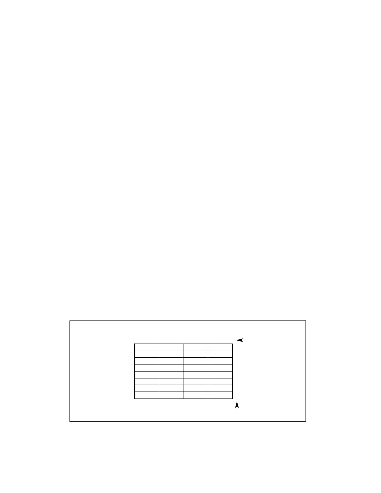
ABOUT THIS MANUAL
Chapter 17 - Programming with Intel® Transactional Synchronization Extensions. Describes the instruc-
tion extensions that support lock elision techniques to improve the performance of multi-threaded software with
contended locks.
Chapter 18 - Control-flow Enforcement Technology. Provides an overview of the Control-flow Enforcement
Technology (CET) and gives guidelines for writing code that access these extensions.
Chapter 19 - Programming with Intel® Advanced Matrix Extensions. Provides an overview of the Intel®
Advanced Matrix Extensions and gives guidelines for writing code that access these extensions.
Chapter 20 - Input/Output. Describes the processor’s I/O mechanism, including I/O port addressing, I/O
instructions, and I/O protection mechanisms.
Chapter 21 - Processor Identification and Feature Determination. Describes how to determine the CPU
type and features available in the processor.
Appendix A - EFLAGS Cross-Reference. Summarizes how the IA-32 instructions affect the flags in the EFLAGS
register.
Appendix B - EFLAGS Condition Codes. Summarizes how conditional jump, move, and ‘byte set on condition
code’ instructions use condition code flags (OF, CF, ZF, SF, and PF) in the EFLAGS register.
Appendix C - Floating-Point Exceptions Summary. Summarizes exceptions raised by the x87 FPU floating-
point and SSE/SSE2/SSE3 floating-point instructions.
Appendix D - Guidelines for Writing SIMD Floating-Point Exception Handlers. Gives guidelines for writing
exception handlers for exceptions generated by SSE/SSE2/SSE3 floating-point instructions.
Appendix E - Intel® Memory Protection Extensions. Provides an overview of the Intel® Memory Protection
Extensions, a feature that has been deprecated and will not be available on future processors.
1.3
NOTATIONAL CONVENTIONS
This manual uses specific notation for data-structure formats, for symbolic representation of instructions, and for
hexadecimal and binary numbers. This notation is described below.
1.3.1
Bit and Byte Order
In illustrations of data structures in memory, smaller addresses appear toward the bottom of the figure; addresses
increase toward the top. Bit positions are numbered from right to left. The numerical value of a set bit is equal to
two raised to the power of the bit position. Intel 64 and IA-32 processors are “little endian” machines; this means
the bytes of a word are numbered starting from the least significant byte. See Figure 1-1.
Highest
Data Structure
Address
31
24 23
16 15
8 7
0
Bit offset
28
24
20
16
12
8
4
Lowest
Byte 3
Byte 2
Byte 1
Byte 0
0
Address
Byte Offset
Figure 1-1. Bit and Byte Order
1-6
Vol. 1
ABOUT THIS MANUAL
1.3.2
Reserved Bits and Software Compatibility
In many register and memory layout descriptions, certain bits are marked as reserved. When bits are marked as
reserved, it is essential for compatibility with future processors that software treat these bits as having a future,
though unknown, effect. The behavior of reserved bits should be regarded as not only undefined, but unpredict-
able.
Software should follow these guidelines in dealing with reserved bits:
• Do not depend on the states of any reserved bits when testing the values of registers that contain such bits.
Mask out the reserved bits before testing.
• Do not depend on the states of any reserved bits when storing to memory or to a register.
• Do not depend on the ability to retain information written into any reserved bits.
• When loading a register, always load the reserved bits with the values indicated in the documentation, if any,
or reload them with values previously read from the same register.
NOTE
Avoid any software dependence upon the state of reserved bits in Intel 64 and IA-32 registers.
Depending upon the values of reserved register bits will make software dependent upon the
unspecified manner in which the processor handles these bits. Programs that depend upon
reserved values risk incompatibility with future processors.
1.3.2.1
Instruction Operands
When instructions are represented symbolically, a subset of the IA-32 assembly language is used. In this subset,
an instruction has the following format:
label: mnemonic argument1, argument2, argument3
where:
• A label is an identifier which is followed by a colon.
• A mnemonic is a reserved name for a class of instruction opcodes which have the same function.
• The operands argument1, argument2, and argument3 are optional. There may be from zero to three
operands, depending on the opcode. When present, they take the form of either literals or identifiers for data
items. Operand identifiers are either reserved names of registers or are assumed to be assigned to data items
declared in another part of the program (which may not be shown in the example).
When two operands are present in an arithmetic or logical instruction, the right operand is the source and the left
operand is the destination.
For example:
LOADREG: MOV EAX, SUBTOTAL
In this example, LOADREG is a label, MOV is the mnemonic identifier of an opcode, EAX is the destination operand,
and SUBTOTAL is the source operand. Some assembly languages put the source and destination in reverse order.
1.3.3
Hexadecimal and Binary Numbers
Base 16 (hexadecimal) numbers are represented by a string of hexadecimal digits followed by the character H (for
example, 0F82EH). A hexadecimal digit is a character from the following set: 0, 1, 2, 3, 4, 5, 6, 7, 8, 9, A, B, C, D,
E, and F.
Base 2 (binary) numbers are represented by a string of 1s and 0s, sometimes followed by the character B (for
example, 1010B). The “B” designation is only used in situations where confusion as to the type of number might
arise.
Vol. 1
1-7
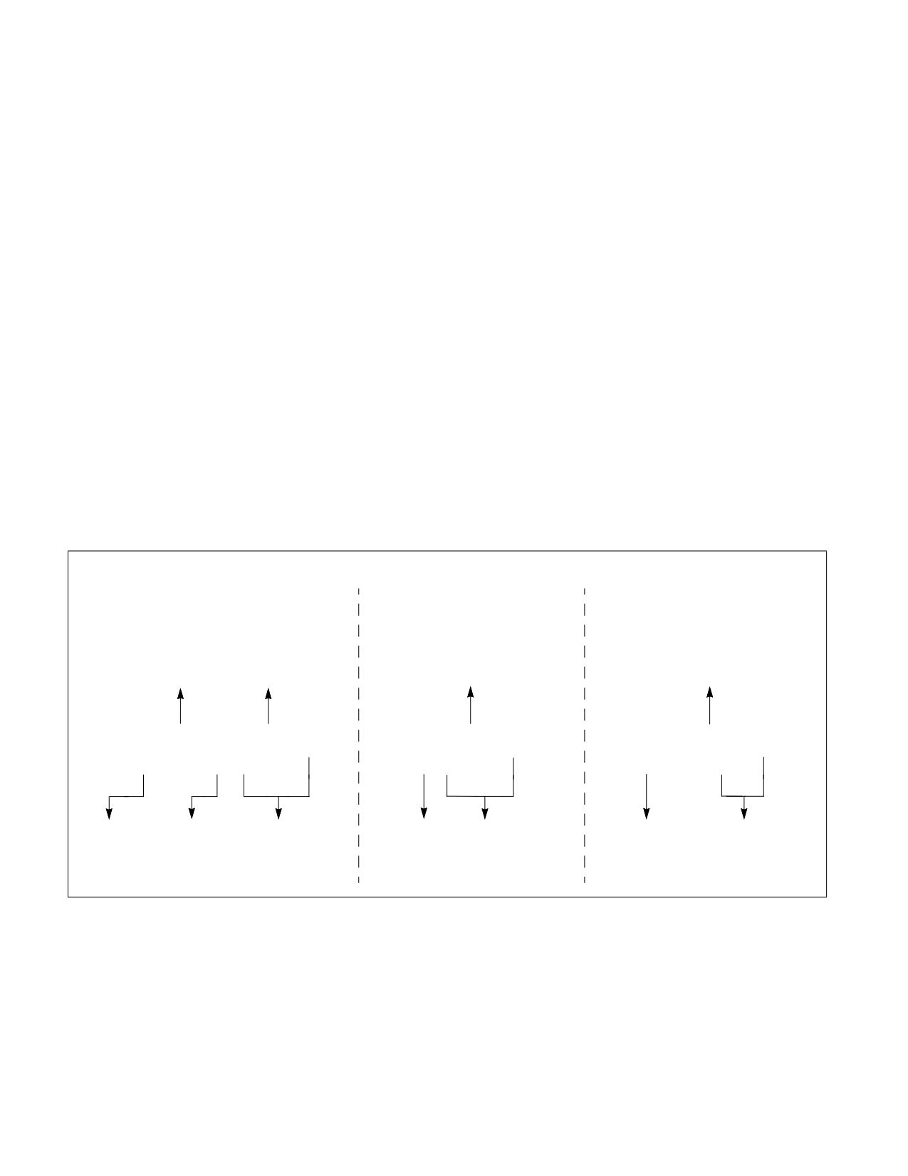
ABOUT THIS MANUAL
1.3.4
Segmented Addressing
The processor uses byte addressing. This means memory is organized and accessed as a sequence of bytes.
Whether one or more bytes are being accessed, a byte address is used to locate the byte or bytes memory. The
range of memory that can be addressed is called an address space.
The processor also supports segmented addressing. This is a form of addressing where a program may have many
independent address spaces, called segments. For example, a program can keep its code (instructions) and stack
in separate segments. Code addresses would always refer to the code space, and stack addresses would always
refer to the stack space. The following notation is used to specify a byte address within a segment:
Segment-register:Byte-address
For example, the following segment address identifies the byte at address FF79H in the segment pointed by the DS
register:
DS:FF79H
The following segment address identifies an instruction address in the code segment. The CS register points to the
code segment and the EIP register contains the address of the instruction.
CS:EIP
1.3.5
A Syntax for CPUID, CR, and MSR Values
Obtain feature flags, status, and system information by using the CPUID instruction, by checking control register
bits, and by reading model-specific registers. See Figure 1-2 for details on the syntax that represents this informa-
tion.
CPUID
Control Registers
Model-Specific Registers
ECX Subleaf
Input Value
Field
Field
Field
(omitted if not used)
Name
Name
Name
CPUID.07H.01H:EAX.SHA512
CR4.OSFXSR
IA32_PAT.PA2
CPUID.07H.01H:EAX.SHA512[0]
CR4.OSFXSR[9]
IA32_PAT.PA2[18:16]
CPUID.07H.01H:EAX[0]
CR4[9]
IA32_PAT[18:16]
EAX Leaf
Output
Bit
Control
Bit
MSR
Bit
Input Value
Register
Position
Register
Position
Name
Position
Name
Figure 1-2. Syntax for CPUID, CR, and MSR Data Presentation
1.3.6
Exceptions
An exception is an event that typically occurs when an instruction causes an error. For example, an attempt to
divide by zero generates an exception. However, some exceptions, such as breakpoints, occur under other condi-
tions. Some types of exceptions may provide error codes. An error code reports additional information about the
error. An example of the notation used to show an exception and error code is shown below:
1-8
Vol. 1
ABOUT THIS MANUAL
#PF(fault code)
This example refers to a page-fault exception under conditions where an error code naming a type of fault is
reported. Under some conditions, exceptions that produce error codes may not be able to report an accurate code.
In this case, the error code is zero, as shown below for a general-protection exception:
#GP(0)
1.4
RELATED LITERATURE
Literature related to Intel 64 and IA-32 processors is listed and viewable on-line at:
See also:
• The latest security information on Intel® products:
• Software developer resources, guidance, and insights for security advisories:
• The data sheet for a particular Intel 64 or IA-32 processor
• The specification update for a particular Intel 64 or IA-32 processor
• Intel® C++ Compiler documentation and online help:
• Intel® Fortran Compiler documentation and online help:
• Intel® Software Development Tools:
• Intel® 64 and IA-32 Architectures Software Developer’s Manual (in one, four or ten volumes):
• Intel® 64 and IA-32 Architectures Optimization Reference Manual:
tures-optimization.html
• Intel® Trusted Execution Technology Measured Launched Environment Developer’s Guide:
http://www.intel.com/content/www/us/en/software-developers/intel-txt-software-development-guide.html
• Intel® Software Guard Extensions (Intel® SGX) Information:
• Developing Multi-threaded Applications: A Platform Consistent Approach:
tions.pdf
• Using Spin-Loops on Intel® Pentium® 4 Processor and Intel® Xeon® Processor:
• Performance Monitoring Unit Sharing Guide:
Literature related to select features in future Intel processors are available at:
• Intel® Architecture Instruction Set Extensions Programming Reference:
More relevant links are:
• Intel® Developer Zone:
• Developer centers:
Vol. 1
1-9
ABOUT THIS MANUAL
• Processor support general link:
• Intel® Hyper-Threading Technology (Intel® HT Technology):
• Microarchitectural Data Sampling
guidance/technical-documentation/intel-analysis-microarchitectural-data-sampling.html
• Hardware Features and Behavior Related to Speculative Execution
guidance/technical-documentation/hardware-behavior-related-to-speculative-execution.html
1-10
Vol. 1
CHAPTER 2
INTEL® 64 AND IA-32 ARCHITECTURES
2.1
BRIEF HISTORY OF INTEL® 64 AND IA-32 ARCHITECTURES
The following sections provide a summary of the major technical evolutions from IA-32 to Intel 64 architecture:
starting from the Intel 8086 processor to the latest Intel® Core® 2 Duo, Core 2 Quad and Intel Xeon processor
5300 and 7300 series. Object code created for processors released as early as 1978 still executes on the latest
processors in the Intel 64 and IA-32 architecture families.
2.1.1
16-Bit Processors and Segmentation (1978)
The IA-32 architecture family was preceded by 16-bit processors, the 8086 and 8088. The 8086 has 16-bit regis-
ters and a 16-bit external data bus, with 20-bit addressing giving a 1-MByte address space. The 8088 is similar to
the 8086 except it has an 8-bit external data bus.
The 8086/8088 introduced segmentation to the IA-32 architecture. With segmentation, a 16-bit segment register
contains a pointer to a memory segment of up to 64 KBytes. Using four segment registers at a time, 8086/8088
processors are able to address up to 256 KBytes without switching between segments. The 20-bit addresses that
can be formed using a segment register and an additional 16-bit pointer provide a total address range of 1 MByte.
2.1.2
The Intel® 286 Processor (1982)
The Intel 286 processor introduced protected mode operation into the IA-32 architecture. Protected mode uses the
segment register content as selectors or pointers into descriptor tables. Descriptors provide 24-bit base addresses
with a physical memory size of up to 16 MBytes, support for virtual memory management on a segment swapping
basis, and a number of protection mechanisms. These mechanisms include:
• Segment limit checking.
• Read-only and execute-only segment options.
• Four privilege levels.
2.1.3
The Intel386™ Processor (1985)
The Intel386 processor was the first 32-bit processor in the IA-32 architecture family. It introduced 32-bit registers
for use both to hold operands and for addressing. The lower half of each 32-bit Intel386 register retains the prop-
erties of the 16-bit registers of earlier generations, permitting backward compatibility. The processor also provides
a virtual-8086 mode that allows for even greater efficiency when executing programs created for 8086/8088
processors.
In addition, the Intel386 processor has support for:
• A 32-bit address bus that supports up to 4-GBytes of physical memory.
• A segmented-memory model and a flat memory model.
• Paging, with a fixed 4-KByte page size providing a method for virtual memory management.
• Support for parallel stages.
2.1.4
The Intel486™ Processor (1989)
The Intel486™ processor added more parallel execution capability by expanding the Intel386 processor’s instruc-
tion decode and execution units into five pipelined stages. Each stage operates in parallel with the others on up to
five instructions in different stages of execution.
Vol. 1
2-1
INTEL® 64 AND IA-32 ARCHITECTURES
In addition, the processor added:
• An 8-KByte on-chip first-level cache that increased the percent of instructions that could execute at the scalar
rate of one per clock.
• An integrated x87 FPU.
• Power saving and system management capabilities.
2.1.5
The Intel® Pentium® Processor (1993)
The introduction of the Intel Pentium processor added a second execution pipeline to achieve superscalar perfor-
mance (two pipelines, known as u and v, together can execute two instructions per clock). The on-chip first-level
cache doubled, with 8 KBytes devoted to code and another 8 KBytes devoted to data. The data cache uses the MESI
protocol to support more efficient write-back cache in addition to the write-through cache previously used by the
Intel486 processor. Branch prediction with an on-chip branch table was added to increase performance in looping
constructs.
In addition, the processor added:
• Extensions to make the virtual-8086 mode more efficient and allow for 4-MByte as well as 4-KByte pages.
• Internal data paths of 128 and 256 bits add speed to internal data transfers.
• Burstable external data bus was increased to 64 bits.
• An APIC to support systems with multiple processors.
• A dual processor mode to support glueless two processor systems.
A subsequent stepping of the Pentium family introduced Intel MMX technology (the Pentium Processor with MMX
technology). Intel MMX technology uses the single-instruction, multiple-data (SIMD) execution model to perform
parallel computations on packed integer data contained in 64-bit registers.
See Section 2.2.7, “SIMD Instructions.”
2.1.6
The P6 Family of Processors (1995-1999)
The P6 family of processors was based on a superscalar microarchitecture that set new performance standards; see
also Section 2.2.1, “P6 Family Microarchitecture.” One of the goals in the design of the P6 family microarchitecture
was to exceed the performance of the Pentium processor significantly while using the same 0.6-micrometer, four-
layer, metal BICMOS manufacturing process. Members of this family include the following:
• The Intel Pentium Pro processor is three-way superscalar. Using parallel processing techniques, the
processor is able on average to decode, dispatch, and complete execution of (retire) three instructions per
clock cycle. The Pentium Pro introduced the dynamic execution (micro-data flow analysis, out-of-order
execution, superior branch prediction, and speculative execution) in a superscalar implementation. The
processor was further enhanced by its caches. It has the same two on-chip 8-KByte 1st-Level caches as the
Pentium processor and an additional 256-KByte Level 2 cache in the same package as the processor.
• The Intel Pentium II processor added Intel MMX technology to the P6 family processors along with new
packaging and several hardware enhancements. The processor core is packaged in the single edge contact
cartridge (SECC). The Level l data and instruction caches were enlarged to 16 KBytes each, and Level 2 cache
sizes of 256 KBytes, 512 KBytes, and 1 MBytes are supported. A half-frequency backside bus connects the
Level 2 cache to the processor. Multiple low-power states such as AutoHALT, Stop-Grant, Sleep, and Deep Sleep
are supported to conserve power when idling.
• The Pentium II Xeon processor combined the premium characteristics of previous generations of Intel
processors. This includes: 4-way, 8-way (and up) scalability and a 2 MBytes 2nd-Level cache running on a full-
frequency backside bus.
• The Intel Celeron processor family focused on the value PC market segment. Its introduction offers an
integrated 128 KBytes of Level 2 cache and a plastic pin grid array (P.P.G.A.) form factor to lower system design
cost.
• The Intel Pentium III processor introduced the Streaming SIMD Extensions (SSE) to the IA-32 architecture.
SSE extensions expand the SIMD execution model introduced with the Intel MMX technology by providing a
2-2
Vol. 1
INTEL® 64 AND IA-32 ARCHITECTURES
new set of 128-bit registers and the ability to perform SIMD operations on packed single precision floating-
point values. See Section 2.2.7, “SIMD Instructions.”
• The Pentium III Xeon processor extended the performance levels of the IA-32 processors with the
enhancement of a full-speed, on-die, and Advanced Transfer Cache.
2.1.7
The Intel® Pentium® 4 Processor Family (2000-2006)
The Intel Pentium 4 processor family is based on Intel NetBurst microarchitecture; see Section 2.2.2, “Intel
NetBurst® Microarchitecture.”
The Intel Pentium 4 processor introduced Streaming SIMD Extensions 2 (SSE2); see Section 2.2.7, “SIMD Instruc-
tions.” The Intel Pentium 4 processor 3.40 GHz, supporting Hyper-Threading Technology introduced Streaming
SIMD Extensions 3 (SSE3); see Section 2.2.7, “SIMD Instructions.”
Intel 64 architecture was introduced in the Intel Pentium 4 Processor Extreme Edition supporting Hyper-Threading
Technology and in the Intel Pentium 4 Processor 6xx and 5xx sequences.
Intel® Virtualization Technology (Intel® VT) was introduced in the Intel Pentium 4 processor 672 and 662.
2.1.8
The Intel® Xeon® Processor (2001-2007)
Intel Xeon processors (with exception for dual-core Intel Xeon processor LV, Intel Xeon processor 5100 series) are
based on the Intel NetBurst microarchitecture; see Section 2.2.2, “Intel NetBurst® Microarchitecture.” As a family,
this group of IA-32 processors (more recently Intel 64 processors) is designed for use in multi-processor server
systems and high-performance workstations.
The Intel Xeon processor MP introduced support for Intel® Hyper-Threading Technology; see Section 2.2.8, “Intel®
Hyper-Threading Technology.”
The 64-bit Intel Xeon processor 3.60 GHz (with an 800 MHz System Bus) was used to introduce Intel 64 architec-
ture. The Dual-Core Intel Xeon processor includes dual core technology. The Intel Xeon processor 70xx series
includes Intel Virtualization Technology.
The Intel Xeon processor 5100 series introduces power-efficient, high performance Intel Core microarchitecture.
This processor is based on Intel 64 architecture; it includes Intel Virtualization Technology and dual-core tech-
nology. The Intel Xeon processor 3000 series are also based on Intel Core microarchitecture. The Intel Xeon
processor 5300 series introduces four processor cores in a physical package, they are also based on Intel Core
microarchitecture.
2.1.9
The Intel® Pentium® M Processor (2003-2006)
The Intel Pentium M processor family is a high performance, low power mobile processor family with microarchitec-
tural enhancements over previous generations of IA-32 Intel mobile processors. This family is designed for
extending battery life and seamless integration with platform innovations that enable new usage models (such as
extended mobility, ultra thin form-factors, and integrated wireless networking).
Its enhanced microarchitecture includes:
• Support for Intel Architecture with Dynamic Execution.
• A high performance, low-power core manufactured using Intel’s advanced process technology with copper
interconnect.
• On-die, primary 32-KByte instruction cache and 32-KByte write-back data cache.
• On-die, second-level cache (up to 2 MByte) with Advanced Transfer Cache Architecture.
• Advanced Branch Prediction and Data Prefetch Logic.
• Support for MMX technology, Streaming SIMD instructions, and the SSE2 instruction set.
• A 400 or 533 MHz, Source-Synchronous Processor System Bus.
• Advanced power management using Enhanced Intel SpeedStep® technology.
Vol. 1
2-3
INTEL® 64 AND IA-32 ARCHITECTURES
2.1.10 The Intel® Pentium® Processor Extreme Edition (2005)
The Intel Pentium processor Extreme Edition introduced dual-core technology. This technology provides advanced
hardware multi-threading support. The processor is based on Intel NetBurst microarchitecture and supports Intel
SSE, SSE2, SSE3, Intel Hyper-Threading Technology, and Intel 64 architecture.
See also:
• Section 2.2.2, “Intel NetBurst® Microarchitecture.”
• Section 2.2.3, “Intel® Core™ Microarchitecture.”
• Section 2.2.7, “SIMD Instructions.”
• Section 2.2.8, “Intel® Hyper-Threading Technology.”
• Section 2.2.9, “Multi-Core Technology.”
• Section 2.2.10, “Intel® 64 Architecture.”
2.1.11 The Intel® Core™ Duo and Intel® Core™ Solo Processors (2006-2007)
The Intel Core Duo processor offers power-efficient, dual-core performance with a low-power design that extends
battery life. This family and the single-core Intel Core Solo processor offer microarchitectural enhancements over
Pentium M processor family.
Its enhanced microarchitecture includes:
• Intel® Smart Cache which allows for efficient data sharing between two processor cores.
• Improved decoding and SIMD execution.
• Intel® Dynamic Power Coordination and Enhanced Intel® Deeper Sleep to reduce power consumption.
• Intel® Advanced Thermal Manager which features digital thermal sensor interfaces.
• Support for power-optimized 667 MHz bus.
The dual-core Intel Xeon processor LV is based on the same microarchitecture as Intel Core Duo processor, and
supports IA-32 architecture.
2.1.12 The Intel® Xeon® Processor 5100, 5300 Series, and Intel® Core™ 2 Processor Family
(2006)
The Intel Xeon processor 3000, 3200, 5100, 5300, and 7300 series, Intel Pentium Dual-Core, Intel Core 2 Extreme,
Intel Core 2 Quad processors, and Intel Core 2 Duo processor family support Intel 64 architecture; they are based
on the high-performance, power-efficient Intel® Core microarchitecture built on 65 nm process technology. The
Intel Core microarchitecture includes the following innovative features:
• Intel® Wide Dynamic Execution to increase performance and execution throughput.
• Intel® Intelligent Power Capability to reduce power consumption.
• Intel® Advanced Smart Cache which allows for efficient data sharing between two processor cores.
• Intel® Smart Memory Access to increase data bandwidth and hide latency of memory accesses.
• Intel® Advanced Digital Media Boost which improves application performance using multiple generations of
Streaming SIMD extensions.
The Intel Xeon processor 5300 series, Intel Core 2 Extreme processor QX6800 series, and Intel Core 2 Quad
processors support Intel quad-core technology.
2.1.13 The Intel® Xeon® Processor 5200, 5400, 7400 Series, and Intel® Core™ 2 Processor
Family (2007)
The Intel Xeon processor 5200, 5400, and 7400 series, Intel Core 2 Quad processor Q9000 Series, Intel Core 2 Duo
processor E8000 series support Intel 64 architecture; they are based on the Enhanced Intel® Core microarchitec-
2-4
Vol. 1
INTEL® 64 AND IA-32 ARCHITECTURES
ture using 45 nm process technology. The Enhanced Intel Core microarchitecture provides the following improved
features:
• A radix-16 divider, faster OS primitives further increases the performance of Intel® Wide Dynamic Execution.
• Improves Intel® Advanced Smart Cache with Up to 50% larger level-two cache and up to 50% increase in way-
set associativity.
• A 128-bit shuffler engine significantly improves the performance of Intel® Advanced Digital Media Boost and
SSE4.
The Intel Xeon processor 5400 series and the Intel Core 2 Quad processor Q9000 Series support Intel quad-core
technology. The Intel Xeon processor 7400 series offers up to six processor cores and an L3 cache up to 16 MBytes.
2.1.14 The Intel Atom® Processor Family (2008)
The first generation of Intel Atom® processors are built on 45 nm process technology. They are based on a new
microarchitecture, Intel Atom® microarchitecture, which is optimized for ultra low power devices. The Intel Atom®
microarchitecture features two in-order execution pipelines that minimize power consumption, increase battery
life, and enable ultra-small form factors. The initial Intel Atom Processor family and subsequent generations
including Intel Atom processor D2000, N2000, E2000, Z2000, C1000 series provide the following features:
• Enhanced Intel® SpeedStep® Technology.
• Intel® Hyper-Threading Technology.
• Deep Power Down Technology with Dynamic Cache Sizing.
• Support for instruction set extensions up to and including Supplemental Streaming SIMD Extensions 3
(SSSE3).
• Support for Intel® Virtualization Technology.
• Support for Intel® 64 Architecture (excluding Intel Atom processor Z5xx Series).
2.1.15 The Intel Atom® Processor Family Based on Silvermont Microarchitecture (2013)
Intel Atom Processor C2xxx, E3xxx, S1xxx series are based on the Silvermont microarchitecture. Processors based
on the Silvermont microarchitecture support instruction set extensions up to and including SSE4.2, AESNI, and
PCLMULQDQ.
2.1.16 The Intel® Core™ i7 Processor Family (2008)
The Intel Core i7 processor 900 series supports Intel 64 architecture, and is based on Nehalem microarchitecture
using 45 nm process technology. The Intel Core i7 processor and Intel Xeon processor 5500 series include the
following features:
• Intel® Turbo Boost Technology converts thermal headroom into higher performance.
• Intel® HyperThreading Technology in conjunction with Quadcore to provide four cores and eight threads.
• Dedicated power control unit to reduce active and idle power consumption.
• Integrated memory controller on the processor supporting three channels of DDR3 memory.
•
8 MB inclusive Intel® Smart Cache.
• Intel® QuickPath interconnect (QPI) providing point-to-point link to chipset.
• Support for SSE4.2 and SSE4.1 instruction sets.
• Second generation Intel Virtualization Technology.
2.1.17 The Intel® Xeon® Processor 7500 Series (2010)
The Intel Xeon processor 7500 and 6500 series are based on Nehalem microarchitecture using 45 nm process tech-
nology. These processors support the same features described in Section 2.1.16, plus the following features:
Vol. 1
2-5
INTEL® 64 AND IA-32 ARCHITECTURES
• Up to eight cores per physical processor package.
• Up to 24 MB inclusive Intel® Smart Cache.
• Provides Intel® Scalable Memory Interconnect (Intel® SMI) channels with Intel® 7500 Scalable Memory Buffer
to connect to system memory.
• Advanced RAS supporting software recoverable machine check architecture.
2.1.18
2010 Intel® Core™ Processor Family (2010)
The 2010 Intel Core processor family spans Intel Core i7, i5, and i3 processors. These processors are based on
Westmere microarchitecture using 32 nm process technology. The features can include:
• Deliver smart performance using Intel Hyper-Threading Technology plus Intel Turbo Boost Technology.
• Enhanced Intel Smart Cache and integrated memory controller.
• Intelligent power gating.
• Repartitioned platform with on-die integration of 45 nm integrated graphics.
• Range of instruction set support up to AESNI, PCLMULQDQ, SSE4.2 and SSE4.1.
2.1.19 The Intel® Xeon® Processor 5600 Series (2010)
The Intel Xeon processor 5600 series are based on Westmere microarchitecture using 32 nm process technology.
They support the same features described in Section 2.1.16, plus the following features:
• Up to six cores per physical processor package.
• Up to 12 MB enhanced Intel® Smart Cache.
• Support for AESNI, PCLMULQDQ, SSE4.2 and SSE4.1 instruction sets.
• Flexible Intel Virtualization Technologies across processor and I/O.
2.1.20 The Second Generation Intel® Core™ Processor Family (2011)
The Second Generation Intel Core processor family spans Intel Core i7, i5, and i3 processors based on the Sandy
Bridge microarchitecture. These processors are built from 32 nm process technology and have features including:
• Intel Turbo Boost Technology for Intel Core i5 and i7 processors.
• Intel Hyper-Threading Technology.
• Enhanced Intel Smart Cache and integrated memory controller.
• Processor graphics and built-in visual features like Intel® Quick Sync Video, Intel® InsiderTM, etc.
• Range of instruction set support up to AVX, AESNI, PCLMULQDQ, SSE4.2 and SSE4.1.
The Intel Xeon processor E3-1200 product family is also based on the Sandy Bridge microarchitecture.
The Intel Xeon processor E5-2400/1400 product families are based on the Sandy Bridge-EP microarchitecture.
The Intel Xeon processor E5-4600/2600/1600 product families are based on the Sandy Bridge-EP microarchitec-
ture and provide support for multiple sockets.
2.1.21 The Third Generation Intel® Core™ Processor Family (2012)
The Third Generation Intel Core processor family spans Intel Core i7, i5, and i3 processors based on the Ivy Bridge
microarchitecture. The Intel Xeon processor E7-8800/4800/2800 v2 product families and Intel Xeon processor E3-
1200 v2 product family are also based on the Ivy Bridge microarchitecture.
The Intel Xeon processor E5-2400/1400 v2 product families are based on the Ivy Bridge-EP microarchitecture.
The Intel Xeon processor E5-4600/2600/1600 v2 product families are based on the Ivy Bridge-EP microarchitec-
ture and provide support for multiple sockets.
2-6
Vol. 1
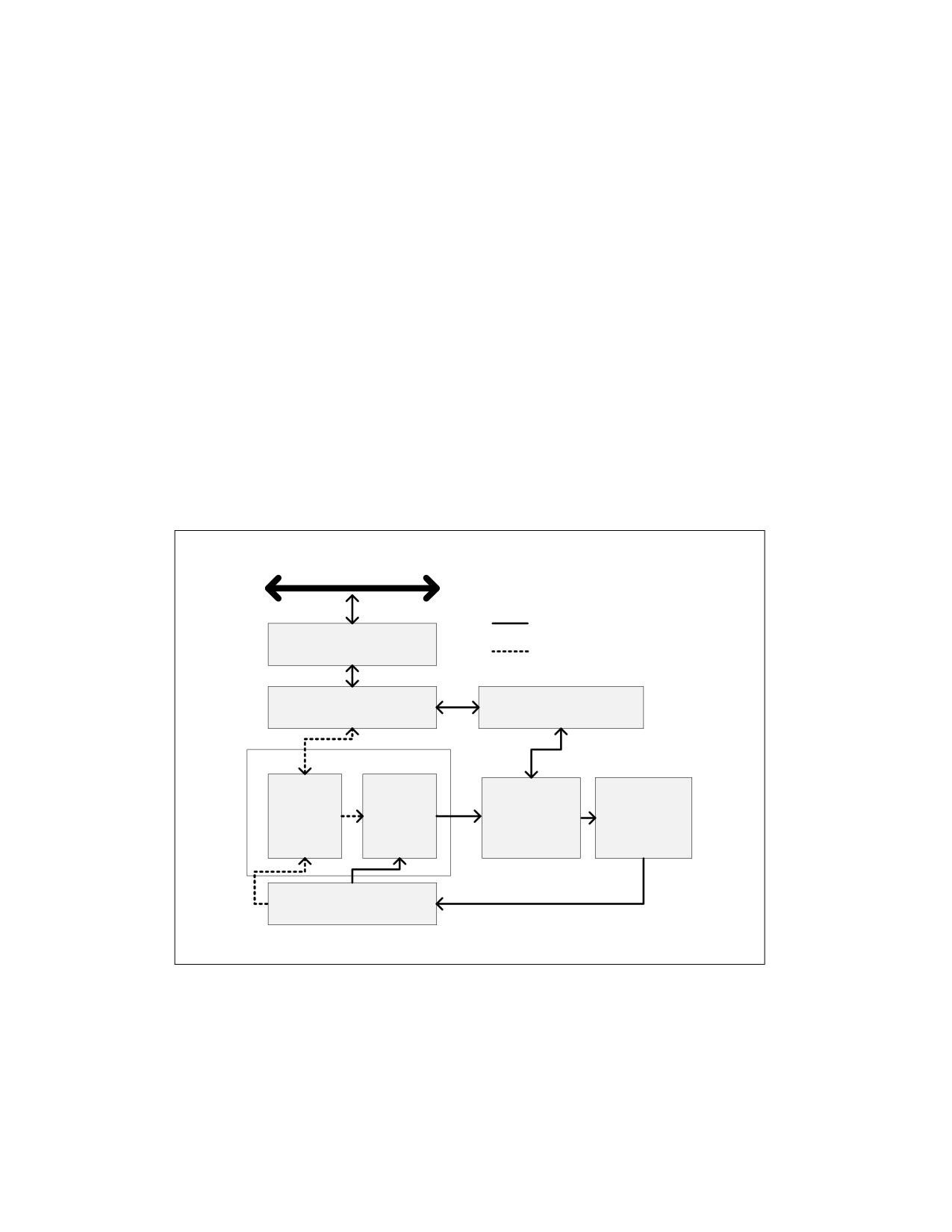
INTEL® 64 AND IA-32 ARCHITECTURES
2.1.22 The Fourth Generation Intel® Core™ Processor Family (2013)
The Fourth Generation Intel Core processor family spans Intel Core i7, i5, and i3 processors based on the Haswell
microarchitecture. Intel Xeon processor E3-1200 v3 product family is also based on the Haswell microarchitecture.
2.2
MORE ON SPECIFIC ADVANCES
The following sections provide more information on major innovations.
2.2.1
P6 Family Microarchitecture
The Pentium Pro processor introduced a new microarchitecture commonly referred to as P6 processor microarchi-
tecture. The P6 processor microarchitecture was later enhanced with an on-die, Level 2 cache, called Advanced
Transfer Cache.
The microarchitecture is a three-way superscalar, pipelined architecture. Three-way superscalar means that by
using parallel processing techniques, the processor is able on average to decode, dispatch, and complete execution
of (retire) three instructions per clock cycle. To handle this level of instruction throughput, the P6 processor family
uses a decoupled, 12-stage superpipeline that supports out-of-order instruction execution.
Figure 2-1 shows a conceptual view of the P6 processor microarchitecture pipeline with the Advanced Transfer
Cache enhancement.
System Bus
Frequently used
Bus Unit
Less frequently used
2nd Level Cache
1st Level Cache
On-die, 8-way
4-way, low latency
Front End
Execution
Instruction
Execution
Fetch/
Cache
Out-of-Order
Retirement
Decode
Microcode
Core
ROM
Branch History Update
BTSs/Branch Prediction
OM16520
Figure 2-1. The P6 Processor Microarchitecture with Advanced Transfer Cache Enhancement
To ensure a steady supply of instructions and data for the instruction execution pipeline, the P6 processor microar-
chitecture incorporates two cache levels. The Level 1 cache provides an 8-KByte instruction cache and an 8-KByte
data cache, both closely coupled to the pipeline. The Level 2 cache provides 256-KByte, 512-KByte, or 1-MByte
static RAM that is coupled to the core processor through a full clock-speed 64-bit cache bus.
The centerpiece of the P6 processor microarchitecture is an out-of-order execution mechanism called dynamic
execution. Dynamic execution incorporates three data-processing concepts:
Vol. 1
2-7
INTEL® 64 AND IA-32 ARCHITECTURES
• Deep branch prediction allows the processor to decode instructions beyond branches to keep the instruction
pipeline full. The P6 processor family implements highly optimized branch prediction algorithms to predict the
direction of the instruction.
• Dynamic data flow analysis requires real-time analysis of the flow of data through the processor to
determine dependencies and to detect opportunities for out-of-order instruction execution. The out-of-order
execution core can monitor many instructions and execute these instructions in the order that best optimizes
the use of the processor’s multiple execution units, while maintaining the data integrity.
• Speculative execution refers to the processor’s ability to execute instructions that lie beyond a conditional
branch that has not yet been resolved, and ultimately to commit the results in the order of the original
instruction stream. To make speculative execution possible, the P6 processor microarchitecture decouples the
dispatch and execution of instructions from the commitment of results. The processor’s out-of-order execution
core uses data-flow analysis to execute all available instructions in the instruction pool and store the results in
temporary registers. The retirement unit then linearly searches the instruction pool for completed instructions
that no longer have data dependencies with other instructions or unresolved branch predictions. When
completed instructions are found, the retirement unit commits the results of these instructions to memory
and/or the IA-32 registers (the processor’s eight general-purpose registers and eight x87 FPU data registers)
in the order they were originally issued and retires the instructions from the instruction pool.
2.2.2
Intel NetBurst® Microarchitecture
The Intel NetBurst microarchitecture provides:
•
The Rapid Execution Engine.
- Arithmetic Logic Units (ALUs) run at twice the processor frequency.
- Basic integer operations can dispatch in 1/2 processor clock tick.
•
Hyper-Pipelined Technology.
- Deep pipeline to enable industry-leading clock rates for desktop PCs and servers.
- Frequency headroom and scalability to continue leadership into the future.
•
Advanced Dynamic Execution.
- Deep, out-of-order, speculative execution engine.
• Up to 126 instructions in flight.
• Up to 48 loads and 24 stores in pipeline1.
- Enhanced branch prediction capability.
• Reduces the misprediction penalty associated with deeper pipelines.
• Advanced branch prediction algorithm.
• 4K-entry branch target array.
•
New cache subsystem.
- First level caches.
• Advanced Execution Trace Cache stores decoded instructions.
• Execution Trace Cache removes decoder latency from main execution loops.
• Execution Trace Cache integrates path of program execution flow into a single line.
• Low latency data cache.
- Second level cache.
• Full-speed, unified 8-way Level 2 on-die Advance Transfer Cache.
• Bandwidth and performance increases with processor frequency.
1.
Intel 64 and IA-32 processors based on the Intel NetBurst microarchitecture at 90 nm process can handle more than 24 stores in
flight.
2-8
Vol. 1
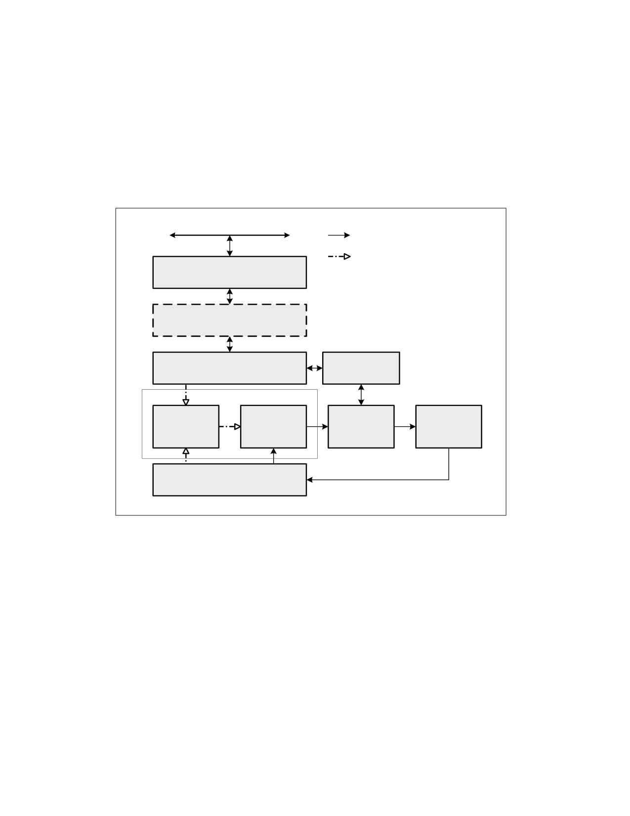
INTEL® 64 AND IA-32 ARCHITECTURES
• High-performance, quad-pumped bus interface to the Intel NetBurst microarchitecture system bus.
- Supports quad-pumped, scalable bus clock to achieve up to 4X effective speed.
- Capable of delivering up to 8.5 GBytes of bandwidth per second.
• Superscalar issue to enable parallelism.
• Expanded hardware registers with renaming to avoid register name space limitations.
•
64-byte cache line size (transfers data up to two lines per sector).
Figure 2-2 is an overview of the Intel NetBurst microarchitecture. This microarchitecture pipeline is made up of
three sections: (1) the front end pipeline, (2) the out-of-order execution core, and (3) the retirement unit.
System Bus
Frequently used paths
Less frequently used
paths
Bus Unit
3rd Level Cache
Optional
2nd Level Cache
1st Level Cache
8-Way
4-way
Front End
Execution
Trace Cache
Fetch/Decode
Out-Of-Order
Retirement
Microcode ROM
Core
Branch History Update
BTBs/Branch Prediction
OM16521
Figure 2-2. The Intel NetBurst® Microarchitecture
2.2.2.1
The Front End Pipeline
The front end supplies instructions in program order to the out-of-order execution core. It performs a number of
functions:
• Prefetches instructions that are likely to be executed.
• Fetches instructions that have not already been prefetched.
• Decodes instructions into micro-operations.
• Generates microcode for complex instructions and special-purpose code.
• Delivers decoded instructions from the execution trace cache.
• Predicts branches using highly advanced algorithm.
The pipeline is designed to address common problems in high-speed, pipelined microprocessors. Two of these
problems contribute to major sources of delays:
• Time to decode instructions fetched from the target.
Vol. 1
2-9
INTEL® 64 AND IA-32 ARCHITECTURES
• Wasted decode bandwidth due to branches or branch target in the middle of cache lines.
The operation of the pipeline’s trace cache addresses these issues. Instructions are constantly being fetched and
decoded by the translation engine (part of the fetch/decode logic) and built into sequences of micro-ops called
traces. At any time, multiple traces (representing prefetched branches) are being stored in the trace cache. The
trace cache is searched for the instruction that follows the active branch. If the instruction also appears as the first
instruction in a pre-fetched branch, the fetch and decode of instructions from the memory hierarchy ceases and the
pre-fetched branch becomes the new source of instructions (see Figure 2-2).
The trace cache and the translation engine have cooperating branch prediction hardware. Branch targets are
predicted based on their linear addresses using branch target buffers (BTBs) and fetched as soon as possible.
2.2.2.2
Out-Of-Order Execution Core
The out-of-order execution core’s ability to execute instructions out of order is a key factor in enabling parallelism.
This feature enables the processor to reorder instructions so that if one micro-op is delayed, other micro-ops may
proceed around it. The processor employs several buffers to smooth the flow of micro-ops.
The core is designed to facilitate parallel execution. It can dispatch up to six micro-ops per cycle (this exceeds trace
cache and retirement micro-op bandwidth). Most pipelines can start executing a new micro-op every cycle, so
several instructions can be in flight at a time for each pipeline. A number of arithmetic logical unit (ALU) instruc-
tions can start at two per cycle; many floating-point instructions can start once every two cycles.
2.2.2.3
Retirement Unit
The retirement unit receives the results of the executed micro-ops from the out-of-order execution core and
processes the results so that the architectural state updates according to the original program order.
When a micro-op completes and writes its result, it is retired. Up to three micro-ops may be retired per cycle. The
Reorder Buffer (ROB) is the unit in the processor which buffers completed micro-ops, updates the architectural
state in order, and manages the ordering of exceptions. The retirement section also keeps track of branches and
sends updated branch target information to the BTB. The BTB then purges pre-fetched traces that are no longer
needed.
2.2.3
Intel® Core™ Microarchitecture
Intel Core microarchitecture introduces the following features that enable high performance and power-efficient
performance for single-threaded as well as multi-threaded workloads:
• Intel® Wide Dynamic Execution enable each processor core to fetch, dispatch, execute in high bandwidths
to support retirement of up to four instructions per cycle.
- Fourteen-stage efficient pipeline.
- Three arithmetic logical units.
- Four decoders to decode up to five instruction per cycle.
- Macro-fusion and micro-fusion to improve front-end throughput.
- Peak issue rate of dispatching up to six micro-ops per cycle.
- Peak retirement bandwidth of up to 4 micro-ops per cycle.
- Advanced branch prediction.
- Stack pointer tracker to improve efficiency of executing function/procedure entries and exits.
• Intel® Advanced Smart Cache delivers higher bandwidth from the second level cache to the core, and
optimal performance and flexibility for single-threaded and multi-threaded applications.
- Large second level cache up to 4 MB and 16-way associativity.
- Optimized for multicore and single-threaded execution environments.
- 256-bit internal data path to improve bandwidth from L2 to first-level data cache.
2-10
Vol. 1
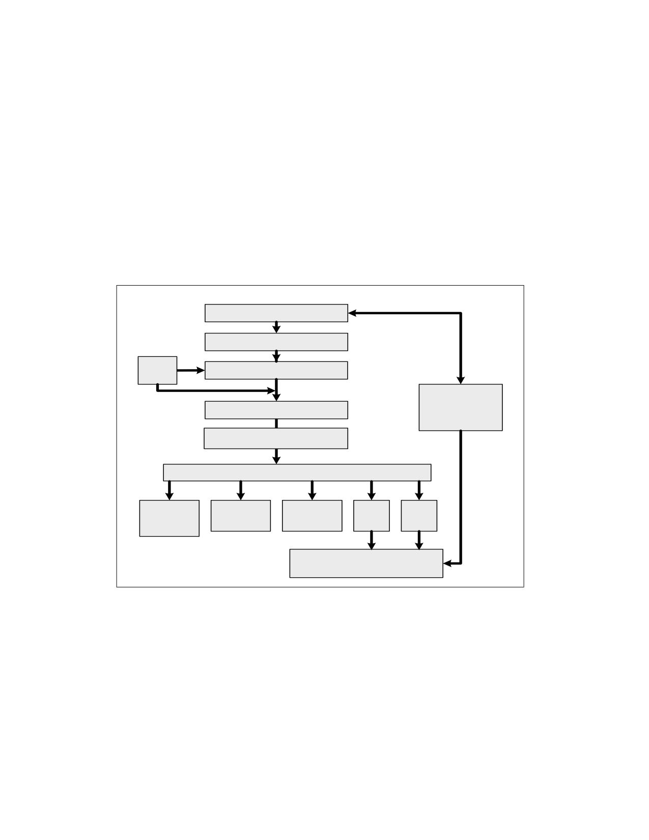
INTEL® 64 AND IA-32 ARCHITECTURES
• Intel® Smart Memory Access prefetches data from memory in response to data access patterns and reduces
cache-miss exposure of out-of-order execution.
- Hardware prefetchers to reduce effective latency of second-level cache misses.
- Hardware prefetchers to reduce effective latency of first-level data cache misses.
- Memory disambiguation to improve efficiency of speculative execution engine.
• Intel® Advanced Digital Media Boost improves most 128-bit SIMD instructions with single-cycle
throughput and floating-point operations.
- Single-cycle throughput of most 128-bit SIMD instructions.
- Up to eight floating-point operations per cycle.
- Three issue ports available to dispatching SIMD instructions for execution.
Intel Core 2 Extreme, Intel Core 2 Duo processors and Intel Xeon processor 5100 series implement two processor
cores based on the Intel Core microarchitecture, the functionality of the subsystems in each core are depicted in
Figure 2-3.
Instruction Fetch and PreDecode
Instruction Queue
Micro-
code
Decode
ROM
Shared L2 Cache
Rename/Alloc
Up to 10.7 GB/s
FSB
Retirement Unit
(Re-Order Buffer)
Scheduler
ALU
ALU
ALU
Branch
FAdd
FMul
Load
Store
MMX/SSE/FP
MMX/SSE
MMX/SSE
Move
L1D Cache and DTLB
Figure 2-3. The Intel® Core™ Microarchitecture Pipeline Functionality
2.2.3.1
The Front End
The front end of Intel Core microarchitecture provides several enhancements to feed the Intel Wide Dynamic
Execution engine:
• Instruction fetch unit prefetches instructions into an instruction queue to maintain steady supply of instruction
to the decode units.
• Four-wide decode unit can decode 4 instructions per cycle or 5 instructions per cycle with Macrofusion.
• Macrofusion fuses common sequence of two instructions as one decoded instruction (micro-ops) to increase
decoding throughput.
• Microfusion fuses common sequence of two micro-ops as one micro-ops to improve retirement throughput.
Vol. 1
2-11
INTEL® 64 AND IA-32 ARCHITECTURES
• Instruction queue provides caching of short loops to improve efficiency.
• Stack pointer tracker improves efficiency of executing procedure/function entries and exits.
• Branch prediction unit employs dedicated hardware to handle different types of branches for improved branch
prediction.
• Advanced branch prediction algorithm directs instruction fetch unit to fetch instructions likely in the architec-
tural code path for decoding.
2.2.3.2
Execution Core
The execution core of the Intel Core microarchitecture is superscalar and can process instructions out of order to
increase the overall rate of instructions executed per cycle (IPC). The execution core employs the following feature
to improve execution throughput and efficiency:
• Up to six micro-ops can be dispatched to execute per cycle.
• Up to four instructions can be retired per cycle.
• Three full arithmetic logical units.
• SIMD instructions can be dispatched through three issue ports.
• Most SIMD instructions have 1-cycle throughput (including 128-bit SIMD instructions).
• Up to eight floating-point operation per cycle.
• Many long-latency computation operation are pipelined in hardware to increase overall throughput.
• Reduced exposure to data access delays using Intel Smart Memory Access.
2.2.4
Intel Atom® Microarchitecture
Intel Atom microarchitecture maximizes power-efficient performance for single-threaded and multi-threaded
workloads by providing:
• Advanced Micro-Ops Execution
- Single-micro-op instruction execution from decode to retirement, including instructions with register-only,
load, and store semantics.
- Sixteen-stage, in-order pipeline optimized for throughput and reduced power consumption.
- Dual pipelines to enable decode, issue, execution, and retirement of two instructions per cycle.
- Advanced stack pointer to improve efficiency of executing function entry/returns.
• Intel® Smart Cache
- Second level cache is 512 KB and 8-way associativity.
- Optimized for multi-threaded and single-threaded execution environments
- 256-bit internal data path between L2 and L1 data caches improves high bandwidth.
• Efficient Memory Access
- Efficient hardware prefetchers to L1 and L2, speculatively loading data likely to be requested by processor
to reduce cache miss impact.
• Intel® Digital Media Boost
- Two issue ports for dispatching SIMD instructions to execution units.
- Single-cycle throughput for most 128-bit integer SIMD instructions.
- Up to six floating-point operations per cycle.
- Up to two 128-bit SIMD integer operations per cycle.
- Safe Instruction Recognition (SIR) to allow long-latency floating-point operations to retire out of order with
respect to integer instructions.
2-12
Vol. 1
INTEL® 64 AND IA-32 ARCHITECTURES
2.2.5
Nehalem Microarchitecture
Nehalem microarchitecture provides the foundation for many features of Intel Core i7 processors. It builds on the
success of 45 nm Intel Core microarchitecture and provides the following feature enhancements:
• Enhanced processor core
- Improved branch prediction and recovery from misprediction.
- Enhanced loop streaming to improve front end performance and reduce power consumption.
- Deeper buffering in out-of-order engine to extract parallelism.
- Enhanced execution units to provide acceleration in CRC, string/text processing and data shuffling.
• Smart Memory Access
- Integrated memory controller provides low-latency access to system memory and scalable memory
bandwidth.
- New cache hierarchy organization with shared, inclusive L3 to reduce snoop traffic.
- Two level TLBs and increased TLB size.
- Fast unaligned memory access.
• HyperThreading Technology
- Provides two hardware threads (logical processors) per core.
- Takes advantage of 4-wide execution engine, large L3, and massive memory bandwidth.
• Dedicated Power management Innovations
- Integrated microcontroller with optimized embedded firmware to manage power consumption.
- Embedded real-time sensors for temperature, current, and power.
- Integrated power gate to turn off/on per-core power consumption
- Versatility to reduce power consumption of memory, link subsystems.
2.2.6
Sandy Bridge Microarchitecture
Sandy Bridge microarchitecture builds on the successes of Intel® Core™ microarchitecture and Nehalem microar-
chitecture. It offers the following features:
• Intel Advanced Vector Extensions (Intel AVX).
- 256-bit floating-point instruction set extensions to the 128-bit Intel Streaming SIMD Extensions, providing
up to 2X performance benefits relative to 128-bit code.
- Non-destructive destination encoding offers more flexible coding techniques.
- Supports flexible migration and co-existence between 256-bit AVX code, 128-bit AVX code and legacy 128-
bit SSE code.
• Enhanced front-end and execution engine.
- New decoded Icache component that improves front-end bandwidth and reduces branch misprediction
penalty.
- Advanced branch prediction.
- Additional macro-fusion support.
- Larger dynamic execution window.
- Multi-precision integer arithmetic enhancements (ADC/SBB, MUL/IMUL).
- LEA bandwidth improvement.
- Reduction of general execution stalls (read ports, writeback conflicts, bypass latency, partial stalls).
- Fast floating-point exception handling.
Vol. 1
2-13
INTEL® 64 AND IA-32 ARCHITECTURES
- XSAVE/XRSTORE performance improvements and XSAVEOPT new instruction.
• Cache hierarchy improvements for wider data path.
- Doubling of bandwidth enabled by two symmetric ports for memory operation.
- Simultaneous handling of more in-flight loads and stores enabled by increased buffers.
- Internal bandwidth of two loads and one store each cycle.
- Improved prefetching.
- High bandwidth low latency LLC architecture.
- High bandwidth ring architecture of on-die interconnect.
For additional information on Intel® Advanced Vector Extensions (AVX), see Section 5.13, “Intel® Advanced Vector
Extensions (Intel® AVX)” and Chapter 14, “Programming with Intel® AVX, FMA, and Intel® AVX2” in the Intel® 64
and IA-32 Architectures Software Developer’s Manual, Volume 1.
2.2.7
SIMD Instructions
Beginning with the Pentium II and Pentium with Intel MMX technology processor families, six extensions have been
introduced into the Intel 64 and IA-32 architectures to perform single-instruction multiple-data (SIMD) operations.
These extensions include the MMX technology, SSE extensions, SSE2 extensions, SSE3 extensions, Supplemental
Streaming SIMD Extensions 3, and SSE4. Each of these extensions provides a group of instructions that perform
SIMD operations on packed integer and/or packed floating-point data elements.
SIMD integer operations can use the 64-bit MMX or the 128-bit XMM registers. SIMD floating-point operations use
128-bit XMM registers. Figure 2-4 shows a summary of the various SIMD extensions (MMX technology, Intel SSE,
Intel SSE2, Intel SSE3, SSSE3, and Intel SSE4), the data types they operate on, and how the data types are packed
into MMX and XMM registers.
The Intel MMX technology was introduced in the Pentium II and Pentium with MMX technology processor families.
MMX instructions perform SIMD operations on packed byte, word, or doubleword integers located in MMX registers.
These instructions are useful in applications that operate on integer arrays and streams of integer data that lend
themselves to SIMD processing.
Intel SSE was introduced in the Pentium III processor family. Intel SSE instructions operate on packed single preci-
sion floating-point values contained in XMM registers and on packed integers contained in MMX registers. Several
Intel SSE instructions provide state management, cache control, and memory ordering operations. Other Intel SSE
instructions are targeted at applications that operate on arrays of single precision floating-point data elements (3-
D geometry, 3-D rendering, and video encoding and decoding applications).
Intel SSE2 was introduced in the Pentium 4 and Intel Xeon processors. Intel SSE2 instructions operate on packed
double precision floating-point values contained in XMM registers and on packed integers contained in MMX and
XMM registers. Intel SSE2 integer instructions extend IA-32 SIMD operations by adding new 128-bit SIMD integer
operations and by expanding existing 64-bit SIMD integer operations to 128-bit XMM capability. Intel SSE2 instruc-
tions also provide new cache control and memory ordering operations.
Intel SSE3 was introduced with the Pentium 4 processor supporting Hyper-Threading Technology (built on 90 nm
process technology). Intel SSE3 offers 13 instructions that accelerate performance of Streaming SIMD Extensions
technology, Streaming SIMD Extensions 2 technology, and x87-FP math capabilities.
SSSE3 was introduced with the Intel Xeon processor 5100 series and Intel Core 2 processor family. SSSE3 offer 32
instructions to accelerate processing of SIMD integer data.
Intel SSE4 offers 54 instructions. 47 of them are referred to as Intel SSE4.1 instructions. Intel SSE4.1 was intro-
duced with the Intel Xeon processor 5400 series and Intel Core 2 Extreme processor QX9650. The other seven Intel
SSE4 instructions are referred to as Intel SSE4.2 instructions.
Intel AES-NI and PCLMULQDQ introduced seven new instructions. Six of them are primitives for accelerating algo-
rithms based on AES encryption/decryption standard, and are referred to as Intel AES-NI.
The PCLMULQDQ instruction accelerates general-purpose block encryption, which can perform carry-less multipli-
cation for two binary numbers up to 64-bit wide.
2-14
Vol. 1
INTEL® 64 AND IA-32 ARCHITECTURES
Intel 64 architecture allows four generations of 128-bit SIMD extensions to access up to 16 XMM registers. IA-32
architecture provides eight XMM registers.
Intel® Advanced Vector Extensions offers comprehensive architectural enhancements over previous generations of
Streaming SIMD Extensions. Intel AVX introduces the following architectural enhancements:
• Support for 256-bit wide vectors and SIMD register set.
•
256-bit floating-point instruction set enhancement with up to 2X performance gain relative to 128-bit
Streaming SIMD extensions.
• Instruction syntax support for generalized three-operand syntax to improve instruction programming flexibility
and efficient encoding of new instruction extensions.
• Enhancement of legacy 128-bit SIMD instruction extensions to support three operand syntax and to simplify
compiler vectorization of high-level language expressions.
• Support flexible deployment of 256-bit AVX code, 128-bit AVX code, legacy 128-bit code and scalar code.
In addition to performance considerations, programmers should also be cognizant of the implications of VEX-
encoded AVX instructions with the expectations of system software components that manage the processor state
components enabled by XCR0. For additional information see Section 2.3.10.1, “Vector Length Transition and
Programming Considerations” in Intel® 64 and IA-32 Architectures Software Developer’s Manual, Volume 2A.
See also:
• Section 5.4, “MMX Instructions,” and Chapter 9, “Programming with Intel® MMX™ Technology.”
• Section 5.5, “Intel® SSE Instructions,” and Chapter 10, “Programming with Intel® Streaming SIMD Extensions
(Intel® SSE).”
• Section 5.6, “Intel® SSE2 Instructions,” and Chapter 11, “Programming with Intel® Streaming SIMD
Extensions 2 (Intel® SSE2).”
• Section 5.7, “Intel® SSE3 Instructions,” Section 5.8, “Supplemental Streaming SIMD Extensions 3 (SSSE3)
Instructions,” Section 5.9, “Intel® SSE4 Instructions,” and Chapter 12, “Programming with Intel® SSE3,
SSSE3, Intel® SSE4, and Intel® AES-NI.”
Vol. 1
2-15
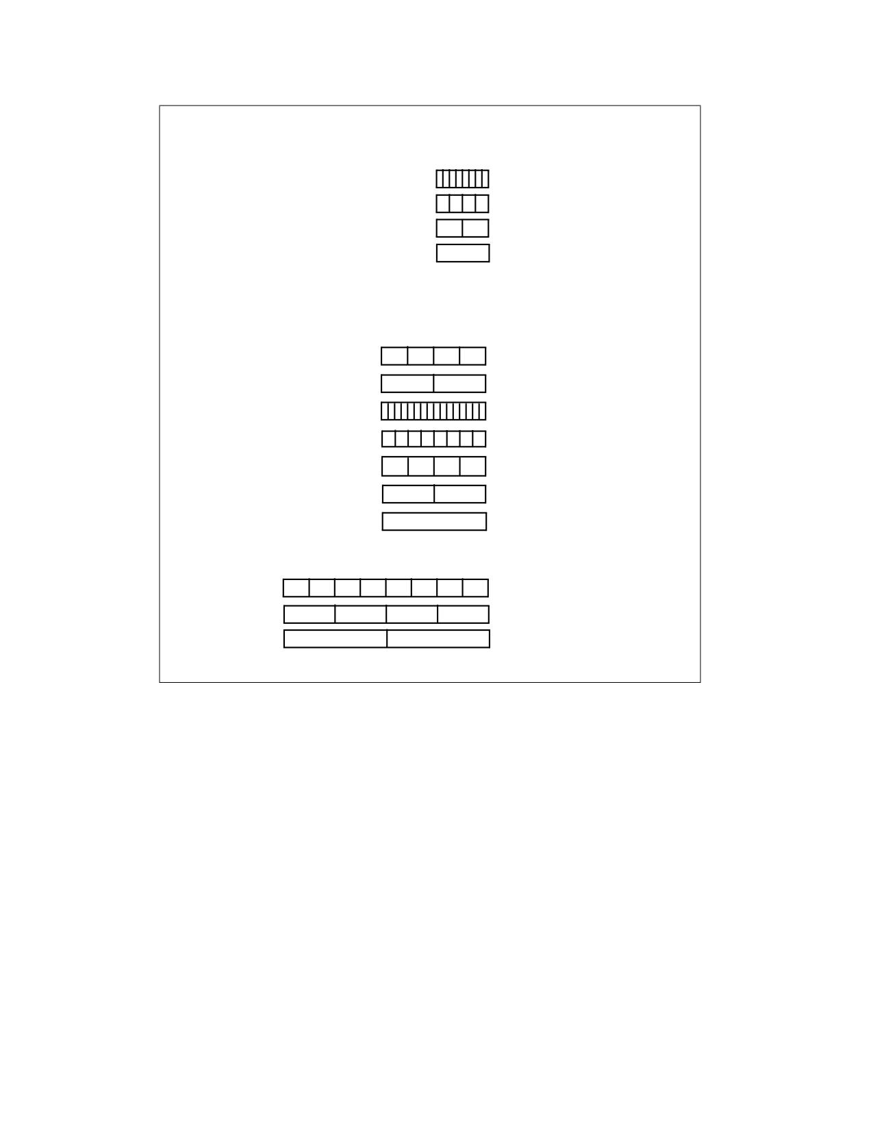
INTEL® 64 AND IA-32 ARCHITECTURES
SIMD Extension
Register Layout
Data Type
MMX Registers
MMX Technology - SSSE3
8 Packed Byte Integers
4 Packed Word Integers
2 Packed Doubleword Integers
Quadword
SSE - AVX
XMM Registers
4 Packed Single Precision
Floating-Point Values
2 Packed Double Precision
Floating-Point Values
16 Packed Byte Integers
8 Packed Word Integers
4 Packed Doubleword
Integers
2 Quadword Integers
Double Quadword
AVX
YMM Registers
8 Packed SP FP Values
4 Packed DP FP Values
2 128-bit Data
Figure 2-4. SIMD Extensions, Register Layouts, and Data Types
2.2.8
Intel® Hyper-Threading Technology
Intel Hyper-Threading Technology (Intel HT Technology) was developed to improve the performance of IA-32
processors when executing multi-threaded operating system and application code or single-threaded applications
under multi-tasking environments. The technology enables a single physical processor to execute two or more
separate code streams (threads) concurrently using shared execution resources.
Intel HT Technology is one form of hardware multi-threading capability in IA-32 processor families. It differs from
multi-processor capability using separate physically distinct packages with each physical processor package mated
with a physical socket. Intel HT Technology provides hardware multi-threading capability with a single physical
package by using shared execution resources in a processor core.
Architecturally, an IA-32 processor that supports Intel HT Technology consists of two or more logical processors,
each of which has its own IA-32 architectural state. Each logical processor consists of a full set of IA-32 data regis-
ters, segment registers, control registers, debug registers, and most of the MSRs. Each also has its own advanced
programmable interrupt controller (APIC).
Figure 2-5 shows a comparison of a processor that supports Intel HT Technology (implemented with two logical
processors) and a traditional dual processor system.
2-16
Vol. 1
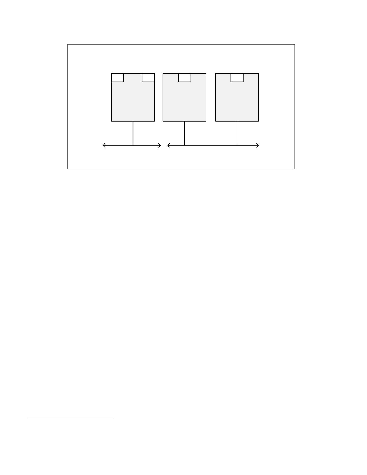
INTEL® 64 AND IA-32 ARCHITECTURES
IA-32 Processor Supporting
Traditional Multiple Processor (MP) System
Hyper-Threading Technology
AS
AS
AS
AS
Processor Core
Processor Core
Processor Core
IA-32 processor
IA-32 processor
IA-32 processor
Two logical
Each processor is a
processors that share
separate physical
a single core
package
AS = IA-32 Architectural State
OM16522
Figure 2-5. Comparison of an IA-32 Processor Supporting Intel® Hyper-Threading Technology
and a Traditional Dual Processor System
Unlike a traditional MP system configuration that uses two or more separate physical IA-32 processors, the logical
processors in an IA-32 processor supporting Intel HT Technology share the core resources of the physical
processor. This includes the execution engine and the system bus interface. After power up and initialization, each
logical processor can be independently directed to execute a specified thread, interrupted, or halted.
Intel HT Technology leverages the process and thread-level parallelism found in contemporary operating systems
and high-performance applications by providing two or more logical processors on a single chip. This configuration
allows two or more threads1 to be executed simultaneously on each a physical processor. Each logical processor
executes instructions from an application thread using the resources in the processor core. The core executes
these threads concurrently, using out-of-order instruction scheduling to maximize the use of execution units during
each clock cycle.
2.2.8.1
Some Implementation Notes
All Intel HT Technology configurations require:
• A processor that supports Intel HT Technology.
• A chipset and BIOS that utilize the technology.
• Operating system optimizations.
At the firmware (BIOS) level, the basic procedures to initialize the logical processors in a processor supporting Intel
HT Technology are the same as those for a traditional DP or MP platform. The mechanisms that are described in the
Multiprocessor Specification, Version 1.4, to power-up and initialize physical processors in an MP system also apply
to logical processors in a processor that supports Intel HT Technology.
An operating system designed to run on a traditional DP or MP platform may use CPUID to determine the presence
of hardware multi-threading support feature and the number of logical processors they provide.
Although existing operating system and application code should run correctly on a processor that supports Intel HT
Technology, some code modifications are recommended to get the optimum benefit. These modifications are
discussed in Chapter 7, “Multiple-Processor Management,” Intel® 64 and IA-32 Architectures Software Developer’s
Manual, Volume 3A.
1. In the remainder of this document, the term “thread” will be used as a general term for the terms “process” and “thread.”
Vol. 1
2-17
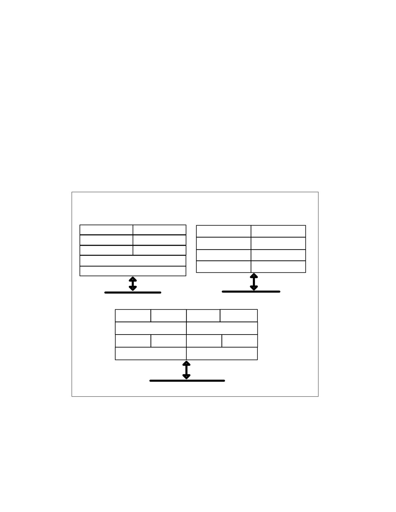
INTEL® 64 AND IA-32 ARCHITECTURES
2.2.9
Multi-Core Technology
Multi-core technology is another form of hardware multi-threading capability in IA-32 processor families. Multi-core
technology enhances hardware multi-threading capability by providing two or more execution cores in a physical
package.
The Intel Pentium processor Extreme Edition is the first member in the IA-32 processor family to introduce multi-
core technology. The processor provides hardware multi-threading support with both two processor cores and Intel
Hyper-Threading Technology. This means that the Intel Pentium processor Extreme Edition provides four logical
processors in a physical package (two logical processors for each processor core). The Dual-Core Intel Xeon
processor features multi-core, Intel Hyper-Threading Technology and supports multi-processor platforms.
The Intel Pentium D processor also features multi-core technology. This processor provides hardware multi-
threading support with two processor cores but does not offer Intel Hyper-Threading Technology. This means that
the Intel Pentium D processor provides two logical processors in a physical package, with each logical processor
owning the complete execution resources of a processor core.
The Intel Core 2 processor family, Intel Xeon processor 3000 series, Intel Xeon processor 5100 series, and Intel
Core Duo processor offer power-efficient multi-core technology. The processor contains two cores that share a
smart second level cache. The Level 2 cache enables efficient data sharing between two cores to reduce memory
traffic to the system bus.
Intel Core Duo Processor
Intel Core 2 Duo Processor
Intel Pentium dual-core Processor
Pentium D Processor
Architectual State
Architectual State
Architectual State
Architectual State
Execution Engine
Execution Engine
Execution Engine
Execution Engine
Local APIC
Local APIC
Local APIC
Local APIC
Second Level Cache
Bus Interface
Bus Interface
Bus Interface
System Bus
System Bus
Pentium Processor Extreme Edition
Architectual
Architectual
Architectual
Architectual
State
State
State
State
Execution Engine
Execution Engine
Local APIC
Local APIC
Local APIC
Local APIC
Bus Interface
Bus Interface
OM19809
System Bus
Figure 2-6. Intel® 64 and IA-32 Processors that Support Dual-Core
The Pentium® dual-core processor is based on the same technology as the Intel Core 2 Duo processor family.
The Intel Xeon processor 7300, 5300, and 3200 series, Intel Core 2 Extreme Quad-Core processor, and Intel Core
2 Quad processors support Intel quad-core technology. The Quad-core Intel Xeon processors and the Quad-Core
Intel Core 2 processor family are also in Figure 2-7.
2-18
Vol. 1
INTEL® 64 AND IA-32 ARCHITECTURES
Intel Core 2 Extreme Quad-core Processor
Intel Core 2 Quad Processor
Intel Xeon Processor 3200 Series
Intel Xeon Processor 5300 Series
Architectual State
Architectual State
Architectual State
Architectual State
Execution Engine
Execution Engine
Execution Engine
Execution Engine
Local APIC
Local APIC
Local APIC
Local APIC
Second Level Cache
Second Level Cache
Bus Interface
Bus Interface
System Bus
OM19810
Figure 2-7. Intel® 64 Processors that Support Quad-Core
Intel Core i7 processors support Intel quad-core technology, Intel HyperThreading Technology, provides Intel
QuickPath interconnect link to the chipset and have integrated memory controller supporting three channels to
DDR3 memory.
Intel Core i7 Processor
Logical
Logical
Logical
Logical
Logical
Logical
Logical
Logical
Proces
Proces
Proces
Proces
Proces
Proces
Proces
Proces
sor
sor
sor
sor
sor
sor
sor
sor
L1 and L2
L1 and L2
L1 and L2
L1 and L2
Execution Engine
Execution Engine
Execution Engine
Execution Engine
Third Level Cache
QuickPath Interconnect (QPI) Interface, Integrated Memory Controller
IMC
QPI
DDR3
Chipset
OM19810b
Figure 2-8. Intel® Core™ i7 Processor
Vol. 1
2-19
INTEL® 64 AND IA-32 ARCHITECTURES
2.2.10 Intel® 64 Architecture
Intel 64 architecture increases the linear address space for software to 64 bits and supports physical address space
up to 52 bits. The technology also introduces a new operating mode referred to as IA-32e mode.
IA-32e mode operates in one of two sub-modes: (1) compatibility mode enables a 64-bit operating system to run
most legacy 32-bit software unmodified, (2) 64-bit mode enables a 64-bit operating system to run applications
written to access 64-bit address space.
In the 64-bit mode, applications may access:
•
64-bit flat linear addressing.
•
8 additional general-purpose registers (GPRs).
•
8 additional registers for streaming SIMD extensions (Intel SSE, SSE2, and SSE3, and SSSE3).
•
64-bit-wide GPRs and instruction pointers.
• Uniform byte-register addressing.
• Fast interrupt-prioritization mechanism.
• A new instruction-pointer relative-addressing mode.
An Intel 64 architecture processor supports existing IA-32 software because it is able to run all non-64-bit legacy
modes supported by IA-32 architecture. Most existing IA-32 applications also run in compatibility mode.
2.2.11 Intel® Virtualization Technology (Intel® VT)
Intel® Virtualization Technology for Intel 64 and IA-32 architectures provide extensions that support virtualization.
The extensions are referred to as Virtual Machine Extensions (VMX). An Intel 64 or IA-32 platform with VMX can
function as multiple virtual systems (or virtual machines). Each virtual machine can run operating systems and
applications in separate partitions.
VMX also provides programming interface for a new layer of system software (called the Virtual Machine Monitor
(VMM)) used to manage the operation of virtual machines. Information on VMX and on the programming of VMMs
is in the Intel® 64 and IA-32 Architectures Software Developer’s Manual, Volume 3C.
Intel Core i7 processor provides the following enhancements to Intel Virtualization Technology:
• Virtual processor ID (VPID) to reduce the cost of VMM managing transitions.
• Extended page table (EPT) to reduce the number of transitions for VMM to manage memory virtualization.
• Reduced latency of VM transitions.
2.3
INTEL® 64 AND IA-32 PROCESSOR GENERATIONS
In the mid-1960s, Intel co-founder and Chairman Emeritus Gordon Moore had this observation: “... the number of
transistors that would be incorporated on a silicon die would double every 18 months for the next several years.”
Over the past three and half decades, this prediction known as “Moore's Law” has continued to hold true.
The computing power and the complexity (or roughly, the number of transistors per processor) of Intel architecture
processors has grown in close relation to Moore's law. By taking advantage of new process technology and new
microarchitecture designs, each new generation of IA-32 processors has demonstrated frequency-scaling head-
room and new performance levels over the previous generation processors.
2-20
Vol. 1
INTEL® 64 AND IA-32 ARCHITECTURES
The key features of the Intel Pentium 4 processor, Intel Xeon processor, Intel Xeon processor MP, Pentium III
processor, and Pentium III Xeon processor with advanced transfer cache are shown in Table 2-1. Older generation
IA-32 processors, which do not employ on-die Level 2 cache, are shown in Table 2-2.
Table 2-1. Key Features of Most Recent IA-32 Processors
Intel
Date
Microarchitecture
Top-Bin Clock
Tran-
Register
System
Max.
On-Die
Processor
Intro-
Frequency at
sistors
Sizes1
Bus Band-
Extern.
Caches2
duced
Introduction
width
Addr.
Space
Intel Pentium
2004
Intel Pentium M
2.00 GHz
140 M
GP: 32
3.2 GB/s
4 GB
L1: 64 KB
M
Processor
FPU: 80
L2: 2 MB
Processor
MMX: 64
7553
XMM: 128
Intel Core Duo
2006
Improved Intel
2.16 GHz
152 M
GP: 32
5.3 GB/s
4 GB
L1: 64 KB
Processor
Pentium M
FPU: 80
L2: 2 MB (2
T2600 3
Processor
MMX: 64
MB Total)
Microarchitecture;
XMM: 128
Dual Core;
Intel Smart Cache,
Advanced Thermal
Manager
Intel Atom
2008
Intel Atom
1.86 GHz -
47 M
GP: 32
Up to 4.2
4 GB
L1: 56 KB4
Processor
Microarchitecture;
800 MHz
FPU: 80
GB/s
L2: 512 KB
Z5xx series
MMX: 64
Intel Virtualization
XMM: 128
Technology.
NOTES:
1. The register size and external data bus size are given in bits.
2. First level cache is denoted using the abbreviation L1, 2nd level cache is denoted as L2. The size of L1 includes the first-level data
cache and the instruction cache where applicable, but does not include the trace cache.
3. Intel processor numbers are not a measure of performance. Processor numbers differentiate features within each processor family,
not across different processor families. See http://www.intel.com/products/processor_number for details.
4. In Intel Atom Processor, the size of L1 instruction cache is 32 KBytes, L1 data cache is 24 KBytes.
Table 2-2. Key Features of Most Recent Intel® 64 Processors
Intel
Date
Micro-architec-
Highest
Tran-
Register
System
Max.
On-Die
Processor
Intro-
ture
Processor
sistors
Sizes
Bus/QPI
Extern.
Caches
duced
Base Fre-
Link
Addr.
quency at
Speed
Space
Intro-
duction
64-bit Intel
2004
Intel NetBurst
3.60 GHz
125 M
GP: 32, 64
6.4 GB/s
64 GB
12K µop
Xeon
Microarchitecture;
FPU: 80
Execution
Processor
Intel Hyper-
MMX: 64
Trace Cache;
with 800 MHz
Threading
XMM: 128
16 KB L1;
System Bus
Technology; Intel
1 MB L2
64 Architecture
64-bit Intel
2005
Intel NetBurst
3.33 GHz
675 M
GP: 32, 64
5.3 GB/s 1
1024 GB
12K µop
Xeon
Microarchitecture;
FPU: 80
(1 TB)
Execution
Processor MP
Intel Hyper-
MMX: 64
Trace Cache;
with 8MB L3
Threading
XMM: 128
16 KB L1;
Technology; Intel
1 MB L2,
64 Architecture
8 MB L3
Vol. 1
2-21
INTEL® 64 AND IA-32 ARCHITECTURES
Table 2-2. Key Features of Most Recent Intel® 64 Processors (Contd.)
Intel
Date
Micro-architec-
Highest
Tran-
Register
System
Max.
On-Die
Processor
Intro-
ture
Processor
sistors
Sizes
Bus/QPI
Extern.
Caches
duced
Base Fre-
Link
Addr.
quency at
Speed
Space
Intro-
duction
Intel Pentium
2005
Intel NetBurst
3.73 GHz
164 M
GP: 32, 64
8.5 GB/s
64 GB
12K µop
4
Microarchitecture;
FPU: 80
Execution
Processor
Intel Hyper-
MMX: 64
Trace Cache;
Extreme
Threading
XMM: 128
16 KB L1;
Edition
Technology; Intel
2 MB L2
Supporting
64 Architecture
Hyper-
Threading
Technology
Intel Pentium
2005
Intel NetBurst
3.20 GHz
230 M
GP: 32, 64
6.4 GB/s
64 GB
12K µop
Processor
Microarchitecture;
FPU: 80
Execution
Extreme
Intel Hyper-
MMX: 64
Trace Cache;
Edition 840
Threading
XMM: 128
16 KB L1;
Technology; Intel
1 MB L2 (2
64 Architecture;
MB Total)
Dual-core 2
Dual-Core Intel
2005
Intel NetBurst
3.00 GHz
321 M
GP: 32, 64
6.4 GB/s
64 GB
12K µop
Xeon
Microarchitecture;
FPU: 80
Execution
Processor
Intel Hyper-
MMX: 64
Trace Cache;
7041
Threading
XMM: 128
16 KB L1;
Technology; Intel
2 MB L2 (4
64 Architecture;
MB Total)
Dual-core 3
Intel Pentium
2005
Intel NetBurst
3.80 GHz
164 M
GP: 32, 64
6.4 GB/s
64 GB
12K µop
4
Microarchitecture;
FPU: 80
Execution
Processor 672
Intel Hyper-
MMX: 64
Trace Cache;
Threading
XMM: 128
16 KB L1;
Technology; Intel
2 MB L2
64 Architecture;
Intel Virtualization
Technology.
Intel Pentium
2006
Intel NetBurst
3.46 GHz
376 M
GP: 32, 64
8.5 GB/s
64 GB
12K µop
Processor
Microarchitecture;
FPU: 80
Execution
Extreme
Intel 64
MMX: 64
Trace Cache;
Edition 955
Architecture; Dual
XMM: 128
16 KB L1;
Core;
2 MB L2
Intel Virtualization
(4 MB Total)
Technology.
Intel Core 2
2006
Intel Core
2.93 GHz
291 M
GP: 32, 64
8.5 GB/s
64 GB
L1: 64 KB
Extreme
Microarchitecture;
FPU: 80
L2: 4 MB (4
Processor
Dual Core;
MMX: 64
MB Total)
X6800
XMM: 128
Intel 64
Architecture;
Intel Virtualization
Technology.
2-22
Vol. 1
INTEL® 64 AND IA-32 ARCHITECTURES
Table 2-2. Key Features of Most Recent Intel® 64 Processors (Contd.)
Intel
Date
Micro-architec-
Highest
Tran-
Register
System
Max.
On-Die
Processor
Intro-
ture
Processor
sistors
Sizes
Bus/QPI
Extern.
Caches
duced
Base Fre-
Link
Addr.
quency at
Speed
Space
Intro-
duction
Intel Xeon
2006
Intel Core
3.00 GHz
291 M
GP: 32, 64
10.6 GB/s
64 GB
L1: 64 KB
Processor
Microarchitecture;
FPU: 80
L2: 4 MB (4
5160
Dual Core;
MMX: 64
MB Total)
XMM: 128
Intel 64
Architecture;
Intel Virtualization
Technology.
Intel Xeon
2006
Intel NetBurst
3.40 GHz
1.3 B
GP: 32, 64
12.8 GB/s
64 GB
L1: 64 KB
Processor
Microarchitecture;
FPU: 80
L2: 1 MB (2
7140
Dual Core;
MMX: 64
MB Total)
XMM: 128
Intel 64
L3: 16 MB
Architecture;
(16 MB
Total)
Intel Virtualization
Technology.
Intel Core 2
2006
Intel Core
2.66 GHz
582 M
GP: 32, 64
8.5 GB/s
64 GB
L1: 64 KB
Extreme
Microarchitecture;
FPU: 80
L2: 4 MB (4
Processor
Quad Core;
MMX: 64
MB Total)
QX6700
XMM: 128
Intel 64
Architecture;
Intel Virtualization
Technology.
Quad-core
2006
Intel Core
2.66 GHz
582 M
GP: 32, 64
10.6 GB/s
256 GB
L1: 64 KB
Intel Xeon
Microarchitecture;
FPU: 80
L2: 4 MB (8
Processor
Quad Core;
MMX: 64
MB Total)
5355
XMM: 128
Intel 64
Architecture;
Intel Virtualization
Technology.
Intel Core 2
2007
Intel Core
3.00 GHz
291 M
GP: 32, 64
10.6 GB/s
64 GB
L1: 64 KB
Duo Processor
Microarchitecture;
FPU: 80
L2: 4 MB (4
E6850
Dual Core;
MMX: 64
MB Total)
Intel 64
XMM: 128
Architecture;
Intel Virtualization
Technology;
Intel Trusted
Execution
Technology
Intel Xeon
2007
Intel Core
2.93 GHz
582 M
GP: 32, 64
8.5 GB/s
1024 GB
L1: 64 KB
Processor
Microarchitecture;
FPU: 80
L2: 4 MB (8
7350
Quad Core;
MMX: 64
MB Total)
XMM: 128
Intel 64
Architecture;
Intel Virtualization
Technology.
Vol. 1
2-23
INTEL® 64 AND IA-32 ARCHITECTURES
Table 2-2. Key Features of Most Recent Intel® 64 Processors (Contd.)
Intel
Date
Micro-architec-
Highest
Tran-
Register
System
Max.
On-Die
Processor
Intro-
ture
Processor
sistors
Sizes
Bus/QPI
Extern.
Caches
duced
Base Fre-
Link
Addr.
quency at
Speed
Space
Intro-
duction
Intel Xeon
2007
Enhanced Intel
3.00 GHz
820 M
GP: 32, 64
12.8 GB/s
256 GB
L1: 64 KB
Processor
Core
FPU: 80
L2: 6 MB (12
5472
Microarchitecture;
MMX: 64
MB Total)
Quad Core;
XMM: 128
Intel 64
Architecture;
Intel Virtualization
Technology.
Intel Atom
2008
Intel Atom
2.0 - 1.60
47 M
GP: 32, 64
Up to 4.2
Up to
L1: 56 KB4
Processor
Microarchitecture;
GHz
FPU: 80
GB/s
64GB
L2: 512 KB
Intel 64
MMX: 64
Architecture;
XMM: 128
Intel Virtualization
Technology.
Intel Xeon
2008
Enhanced Intel
2.67 GHz
1.9 B
GP: 32, 64
8.5 GB/s
1024 GB
L1: 64 KB
Processor
Core
FPU: 80
L2: 3 MB (9
7460
Microarchitecture;
MMX: 64
MB Total)
Six Cores;
XMM: 128
L3: 16 MB
Intel 64
Architecture;
Intel Virtualization
Technology.
Intel Atom
2008
Intel Atom
1.60 GHz
94 M
GP: 32, 64
Up to 4.2
Up to
L1: 56 KB5
Processor 330
Microarchitecture;
FPU: 80
GB/s
64GB
L2: 512 KB
Intel 64
MMX: 64
(1 MB Total)
Architecture;
XMM: 128
Dual core;
Intel Virtualization
Technology.
Intel Core i7-
2008
Nehalem
3.20 GHz
731 M
GP: 32, 64
QPI: 6.4
64 GB
L1: 64 KB
965
microarchitecture;
FPU: 80
GT/s;
L2: 256 KB
Processor
Quadcore;
MMX: 64
Memory:
L3: 8 MB
Extreme
HyperThreading
XMM: 128
25 GB/s
Edition
Technology; Intel
QPI; Intel 64
Architecture;
Intel Virtualization
Technology.
2-24
Vol. 1
INTEL® 64 AND IA-32 ARCHITECTURES
Table 2-2. Key Features of Most Recent Intel® 64 Processors (Contd.)
Intel
Date
Micro-architec-
Highest
Tran-
Register
System
Max.
On-Die
Processor
Intro-
ture
Processor
sistors
Sizes
Bus/QPI
Extern.
Caches
duced
Base Fre-
Link
Addr.
quency at
Speed
Space
Intro-
duction
Intel Core i7-
2010
Intel Turbo Boost
2.66 GHz
383 M
GP: 32, 64
64 GB
L1: 64 KB
620M
Technology,
FPU: 80
L2: 256 KB
Processor
Westmere
MMX: 64
L3: 4 MB
microarchitecture;
XMM: 128
Dual-core;
HyperThreading
Technology; Intel
64 Architecture;
Intel Virtualization
Technology.,
Integrated graphics
Intel Xeon-
2010
Intel Turbo Boost
3.33 GHz
1.1 B
GP: 32, 64
QPI: 6.4
1 TB
L1: 64 KB
Processor
Technology,
FPU: 80
GT/s; 32
L2: 256 KB
5680
Westmere
MMX: 64
GB/s
L3: 12 MB
microarchitecture;
XMM: 128
Six core;
HyperThreading
Technology; Intel
64 Architecture;
Intel Virtualization
Technology.
Intel Xeon-
2010
Intel Turbo Boost
2.26 GHz
2.3 B
GP: 32, 64
QPI: 6.4
16 TB
L1: 64 KB
Processor
Technology,
FPU: 80
GT/s;
L2: 256 KB
7560
Nehalem
MMX: 64
Memory:
L3: 24 MB
microarchitecture;
XMM: 128
76 GB/s
Eight core;
HyperThreading
Technology; Intel
64 Architecture;
Intel Virtualization
Technology.
Intel Core i7-
2011
Intel Turbo Boost
3.40 GHz
995 M
GP: 32, 64
DMI: 5
64 GB
L1: 64 KB
2600K
Technology, Sandy
FPU: 80
GT/s;
L2: 256 KB
Processor
Bridge
MMX: 64
Memory:
L3: 8 MB
microarchitecture;
XMM: 128
21 GB/s
Four core;
YMM: 256
HyperThreading
Technology; Intel
64 Architecture;
Intel Virtualization
Technology.,
Processor graphics,
Quicksync Video
Vol. 1
2-25
INTEL® 64 AND IA-32 ARCHITECTURES
Table 2-2. Key Features of Most Recent Intel® 64 Processors (Contd.)
Intel
Date
Micro-architec-
Highest
Tran-
Register
System
Max.
On-Die
Processor
Intro-
ture
Processor
sistors
Sizes
Bus/QPI
Extern.
Caches
duced
Base Fre-
Link
Addr.
quency at
Speed
Space
Intro-
duction
Intel Xeon-
2011
Intel Turbo Boost
3.50 GHz
GP: 32, 64
DMI: 5
1 TB
L1: 64 KB
Processor E3-
Technology, Sandy
FPU: 80
GT/s;
L2: 256 KB
1280
Bridge
MMX: 64
Memory:
L3: 8 MB
microarchitecture;
XMM: 128
21 GB/s
Four core;
YMM: 256
HyperThreading
Technology; Intel
64 Architecture;
Intel Virtualization
Technology.
Intel Xeon-
2011
Intel Turbo Boost
2.40 GHz
2.2 B
GP: 32, 64
QPI: 6.4
16 TB
L1: 64 KB
Processor E7-
Technology,
FPU: 80
GT/s;
L2: 256 KB
8870
Westmere
MMX: 64
Memory:
L3: 30 MB
microarchitecture;
XMM: 128
102 GB/s
Ten core;
HyperThreading
Technology; Intel
64 Architecture;
Intel Virtualization
Technology.
NOTES:
1. The 64-bit Intel Xeon Processor MP with an 8-MByte L3 supports a multi-processor platform with a dual system bus; this creates a
platform bandwidth with 10.6 GBytes.
2. In Intel Pentium Processor Extreme Edition 840, the size of on-die cache is listed for each core. The total size of L2 in the physical
package in 2 MBytes.
3. In Dual-Core Intel Xeon Processor 7041, the size of on-die cache is listed for each core. The total size of L2 in the physical package in
4 MBytes.
4. In Intel Atom Processor, the size of L1 instruction cache is 32 KBytes, L1 data cache is 24 KBytes.
5. In Intel Atom Processor, the size of L1 instruction cache is 32 KBytes, L1 data cache is 24 KBytes.
2-26
Vol. 1
INTEL® 64 AND IA-32 ARCHITECTURES
Table 2-3. Key Features of Previous Generations of IA-32 Processors
Intel
Date
Max. Clock
Tran-
Register
Ext. Data
Max.
Caches
Processor
Intro-
Frequency/
sistors
Sizes1
Bus Size2
Extern.
duced
Technology at
Addr.
Introduction
Space
8086
1978
8 MHz
29 K
16 GP
16
1 MB
None
Intel 286
1982
12.5 MHz
134 K
16 GP
16
16 MB
Note 3
Intel386 DX
1985
20 MHz
275 K
32 GP
32
4 GB
Note 3
Processor
Intel486 DX
1989
25 MHz
1.2 M
32 GP
32
4 GB
L1: 8 KB
Processor
80 FPU
Pentium Processor
1993
60 MHz
3.1 M
32 GP
64
4 GB
L1: 16 KB
80 FPU
Pentium Pro
1995
200 MHz
5.5 M
32 GP
64
64 GB
L1: 16 KB
Processor
80 FPU
L2: 256 KB or
512 KB
Pentium II Processor
1997
266 MHz
7 M
32 GP
64
64 GB
L1: 32 KB
80 FPU
L2: 256 KB or
64 MMX
512 KB
Pentium III Processor
1999
500 MHz
8.2 M
32 GP
64
64 GB
L1: 32 KB
80 FPU
L2: 512 KB
64 MMX
128 XMM
Pentium III and
1999
700 MHz
28 M
32 GP
64
64 GB
L1: 32 KB
Pentium III Xeon
80 FPU
L2: 256 KB
Processors
64 MMX
128 XMM
Pentium 4 Processor
2000
1.50 GHz, Intel
42 M
32 GP
64
64 GB
12K µop
NetBurst
80 FPU
Execution
Microarchitecture
64 MMX
Trace Cache;
128 XMM
L1: 8 KB
L2: 256 KB
Intel Xeon Processor
2001
1.70 GHz, Intel
42 M
32 GP
64
64 GB
12K µop
NetBurst
80 FPU
Execution
Microarchitecture
64 MMX
Trace Cache;
128 XMM
L1: 8 KB
L2: 512 KB
Intel Xeon Processor
2002
2.20 GHz, Intel
55 M
32 GP
64
64 GB
12K µop
NetBurst
80 FPU
Execution
Microarchitecture,
64 MMX
Trace Cache;
HyperThreading
128 XMM
L1: 8 KB
Technology
L2: 512 KB
Pentium M Processor
2003
1.60 GHz, Intel
77 M
32 GP
64
4 GB
L1: 64 KB
NetBurst
80 FPU
L2: 1 MB
Microarchitecture
64 MMX
128 XMM
Vol. 1
2-27
INTEL® 64 AND IA-32 ARCHITECTURES
Table 2-3. Key Features of Previous Generations of IA-32 Processors (Contd.)
Intel Pentium 4
2004
3.40 GHz, Intel
125 M
32 GP
64
64 GB
12K µop
Processor
NetBurst
80 FPU
Execution
Supporting Hyper-
Microarchitecture,
64 MMX
Trace Cache;
Threading
HyperThreading
128 XMM
L1: 16 KB
Technology at 90 nm
Technology
L2: 1 MB
process
NOTES:
1. The register size and external data bus size are given in bits. Note also that each 32-bit general-purpose (GP) registers can be
addressed as an 8- or a 16-bit data registers in all of the processors.
2. Internal data paths are 2 to 4 times wider than the external data bus for each processor.
2.4
PLANNED REMOVAL OF INTEL® INSTRUCTION SET ARCHITECTURE AND
FEATURES FROM UPCOMING PRODUCTS
This section lists Intel Instruction Set Architecture (ISA) and features that Intel plans to remove from select prod-
ucts starting from a specific year.
Table 2-4. Planned Intel® ISA and Features Removal List
Intel ISA/Feature
Year of Removal
Sub-page write permissions for EPT
2024 onwards
xAPIC mode
2025 onwards
Key Locker
2025 onwards
Uncore PMI. IA32_DEBUGCTL MSR, bit 13 (MSR address 1D9H)
2026 onwards
2.5
INTEL® INSTRUCTION SET ARCHITECTURE AND FEATURES REMOVED
This section lists Intel ISA and features that Intel has already removed for select upcoming products. All sections
relevant to the removed features will be identified as such and may be moved to an archived section in future
Intel® 64 and IA-32 Architectures Software Developer's Manual releases.
Table 2-5. Intel® ISA and Features Removal List
Intel ISA/Feature
Year of Removal
Intel® Memory Protection Extensions (Intel® MPX)
2019 onwards
MSR_TEST_CTRL, bit 31 (MSR address 33H)
2019 onwards
Hardware Lock Elision (HLE)
2019 onwards
VP2INTERSECT
2023 onwards
2-28
Vol. 1
CHAPTER 3
BASIC EXECUTION ENVIRONMENT
This chapter describes the basic execution environment of an Intel 64 or IA-32 processor as seen by assembly-
language programmers. It describes how the processor executes instructions and how it stores and manipulates
data. The execution environment described here includes memory (the address space), general-purpose data
registers, segment registers, the flag register, and the instruction pointer register.
3.1
MODES OF OPERATION
The IA-32 architecture supports three basic operating modes: protected mode, real-address mode, and system
management mode. The operating mode determines which instructions and architectural features are accessible:
• Protected mode - This mode is the native state of the processor. Among the capabilities of protected mode
is the ability to directly execute “real-address mode” 8086 software in a protected, multi-tasking environment.
This feature is called virtual-8086 mode, although it is not actually a processor mode. Virtual-8086 mode is
actually a protected mode attribute that can be enabled for any task.
• Real-address mode - This mode implements the programming environment of the Intel 8086 processor with
extensions (such as the ability to switch to protected or system management mode). The processor is placed in
real-address mode following power-up or a reset.
• System management mode (SMM) - This mode provides an operating system or executive with a
transparent mechanism for implementing platform-specific functions such as power management and system
security. The processor enters SMM when the external SMM interrupt pin (SMI#) is activated or an SMI is
received from the advanced programmable interrupt controller (APIC).
In SMM, the processor switches to a separate address space while saving the basic context of the currently
running program or task. SMM-specific code may then be executed transparently. Upon returning from SMM,
the processor is placed back into its state prior to the system management interrupt. SMM was introduced with
the Intel386™ SL and Intel486™ SL processors and became a standard IA-32 feature with the Pentium
processor family.
3.1.1
Intel® 64 Architecture
Intel 64 architecture adds IA-32e mode. IA-32e mode has two sub-modes.
These are:
• Compatibility mode (sub-mode of IA-32e mode) - Compatibility mode permits most legacy 16-bit and
32-bit applications to run without re-compilation under a 64-bit operating system. For brevity, the compatibility
sub-mode is referred to as compatibility mode in IA-32 architecture. The execution environment of compati-
bility mode is the same as described in Section 3.2. Compatibility mode also supports all of the privilege levels
that are supported in 64-bit and protected modes. Legacy applications that run in Virtual 8086 mode or use
hardware task management will not work in this mode.
Compatibility mode is enabled by the operating system (OS) on a code segment basis. This means that a single
64-bit OS can support 64-bit applications running in 64-bit mode and support legacy 32-bit applications (not
recompiled for 64-bits) running in compatibility mode.
Compatibility mode is similar to 32-bit protected mode. Applications access only the first 4 GByte of linear-
address space. Compatibility mode uses 16-bit and 32-bit address and operand sizes. Like protected mode, this
mode allows applications to access physical memory greater than 4 GByte using PAE (Physical Address Exten-
sions).
•
64-bit mode (sub-mode of IA-32e mode) - This mode enables a 64-bit operating system to run applica-
tions written to access 64-bit linear address space. For brevity, the 64-bit sub-mode is referred to as 64-bit
mode in IA-32 architecture.
Vol. 1
3-1
BASIC EXECUTION ENVIRONMENT
64-bit mode extends the number of general purpose registers and SIMD extension registers from 8 to 16.
General purpose registers are widened to 64 bits. The mode also introduces a new opcode prefix (REX) to
access the register extensions. See Section 3.2.1 for a detailed description.
64-bit mode is enabled by the operating system on a code-segment basis. Its default address size is 64 bits and
its default operand size is 32 bits. The default operand size can be overridden on an instruction-by-instruction
basis using a REX opcode prefix in conjunction with an operand size override prefix.
REX prefixes allow a 64-bit operand to be specified when operating in 64-bit mode. By using this mechanism,
many existing instructions have been promoted to allow the use of 64-bit registers and 64-bit addresses.
3.2
OVERVIEW OF THE BASIC EXECUTION ENVIRONMENT
Any program or task running on an IA-32 processor is given a set of resources for executing instructions and for
storing code, data, and state information. These resources (described briefly in the following paragraphs and
shown in Figure 3-1) make up the basic execution environment for an IA-32 processor.
An Intel 64 processor supports the basic execution environment of an IA-32 processor, and a similar environment
under IA-32e mode that can execute 64-bit programs (64-bit sub-mode) and 32-bit programs (compatibility sub-
mode).
The basic execution environment is used jointly by the application programs and the operating system or executive
running on the processor.
• Address space - Any task or program running on an IA-32 processor can address a linear address space of
up to 4 GBytes (232 bytes) and a physical address space of up to 64 GBytes (236 bytes). See Section 3.3.6,
“Extended Physical Addressing in Protected Mode,” for more information about addressing an address space
greater than 4 GBytes.
• Basic program execution registers - The eight general-purpose registers, the six segment registers, the
EFLAGS register, and the EIP (instruction pointer) register comprise a basic execution environment in which to
execute a set of general-purpose instructions. These instructions perform basic integer arithmetic on byte,
word, and doubleword integers, handle program flow control, operate on bit and byte strings, and address
memory. See Section 3.4, “Basic Program Execution Registers,” for more information about these registers.
• x87 FPU registers - The eight x87 FPU data registers, the x87 FPU control register, the status register, the
x87 FPU instruction pointer register, the x87 FPU operand (data) pointer register, the x87 FPU tag register, and
the x87 FPU opcode register provide an execution environment for operating on single precision, double
precision, and double extended precision floating-point values, word integers, doubleword integers, quadword
integers, and binary coded decimal (BCD) values. See Section 8.1, “x87 FPU Execution Environment,” for more
information about these registers.
• MMX registers - The eight MMX registers support execution of single-instruction, multiple-data (SIMD)
operations on 64-bit packed byte, word, and doubleword integers. See Section 9.2, “The MMX Technology
Programming Environment,” for more information about these registers.
• XMM registers - The eight XMM data registers and the MXCSR register support execution of SIMD operations
on 128-bit packed single precision and double precision floating-point values and on 128-bit packed byte, word,
doubleword, and quadword integers. See Section 10.2, “Intel® SSE Programming Environment,” for more
information about these registers.
• YMM registers - The YMM data registers support execution of 256-bit SIMD operations on 256-bit packed
single precision and double precision floating-point values and on 256-bit packed byte, word, doubleword, and
quadword integers.
• Bounds registers - Each of the BND0-BND3 register stores the lower and upper bounds (64 bits each)
associated with the pointer to a memory buffer. They support execution of the Intel MPX instructions.
• BNDCFGU and BNDSTATUS- BNDCFGU configures user mode MPX operations on bounds checking.
BNDSTATUS provides additional information on the #BR caused by an MPX operation.
3-2
Vol. 1
BASIC EXECUTION ENVIRONMENT
Basic Program Execution Registers
Address Space*
2^32 -1
Eight 32-bit
Registers
General-Purpose Registers
Six 16-bit
Segment Registers
Registers
32-bits
EFLAGS Register
32-bits
EIP (Instruction Pointer Register)
FPU Registers
Eight 80-bit
Floating-Point
Registers
Data Registers
0
*The address space can be
16 bits Control Register
flat or segmented. Using
16 bits Status Register
the physical address
extension mechanism, a
16 bits Tag Register
physical address space of
2^36 - 1 can be addressed.
Opcode Register (11-bits)
48 bits
FPU Instruction Pointer Register
48 bits
FPU Data (Operand) Pointer Register
Bounds Registers
MMX Registers
Eight 64-bit
Four 128-bit Registers
Registers
MMX Registers
BNDCFGU
BNDSTATUS
XMM Registers
Eight 128-bit
Registers
XMM Registers
32-bits
MXCSR Register
YMM Registers
Eight 256-bit
Registers
YMM Registers
Figure 3-1. IA-32 Basic Execution Environment for Non-64-Bit Modes
Vol. 1
3-3
BASIC EXECUTION ENVIRONMENT
• Stack - To support procedure or subroutine calls and the passing of parameters between procedures or
subroutines, a stack and stack management resources are included in the execution environment. The stack
(not shown in Figure 3-1) is located in memory. See Section 6.2, “Stacks,” for more information about stack
structure.
In addition to the resources provided in the basic execution environment, the IA-32 architecture provides the
following resources as part of its system-level architecture. They provide extensive support for operating-system
and system-development software. Except for the I/O ports, the system resources are described in detail in the
Intel® 64 and IA-32 Architectures Software Developer’s Manual, Volumes 3A, 3B, 3C & 3D.
• I/O ports - The IA-32 architecture supports a transfers of data to and from input/output (I/O) ports. See
Chapter 20, “Input/Output,” in this volume.
• Control registers - The five control registers (CR0 through CR4) determine the operating mode of the
processor and the characteristics of the currently executing task. See Chapter 2, “System Architecture
Overview,” in the Intel® 64 and IA-32 Architectures Software Developer’s Manual, Volume 3A.
• Memory management registers - The GDTR, IDTR, task register, and LDTR specify the locations of data
structures used in protected mode memory management. See Chapter 2, “System Architecture Overview,” in
the Intel® 64 and IA-32 Architectures Software Developer’s Manual, Volume 3A.
• Debug registers - The debug registers (DR0 through DR7) control and allow monitoring of the processor’s
debugging operations. See in the Intel® 64 and IA-32 Architectures Software Developer’s Manual, Volume 3B.
• Memory type range registers (MTRRs) - The MTRRs are used to assign memory types to regions of
memory. See the sections on MTRRs in the Intel® 64 and IA-32 Architectures Software Developer’s Manual,
Volumes 3A, 3B, 3C & 3D.
• Model-specific registers (MSRs) - The processor provides a variety of model-specific registers that are
used to control and report on processor performance. Virtually all MSRs handle system related functions and
are not accessible to an application program. One exception to this rule is the time-stamp counter. The MSRs
are described in Chapter 2, “Model-Specific Registers (MSRs),” of the Intel® 64 and IA-32 Architectures
Software Developer’s Manual, Volume 4.
• Machine check registers - The machine check registers consist of a set of control, status, and error-
reporting MSRs that are used to detect and report on hardware (machine) errors. See Chapter 18, “Machine-
Check Architecture,” of the Intel® 64 and IA-32 Architectures Software Developer’s Manual, Volume 3A.
• Performance monitoring counters - The performance monitoring counters allow processor performance
events to be monitored. See Chapter 22, “Performance Monitoring,” in the Intel® 64 and IA-32 Architectures
Software Developer’s Manual, Volume 3B.
The remainder of this chapter describes the organization of memory and the address space, the basic program
execution registers, and addressing modes. Refer to the following chapters in this volume for descriptions of the
other program execution resources shown in Figure 3-1:
• X87 FPU registers - See Chapter 8, “Programming with the x87 FPU.”
• MMX Registers - See Chapter 9, “Programming with Intel® MMX™ Technology.”
• XMM registers - See Chapter 10, “Programming with Intel® Streaming SIMD Extensions (Intel® SSE),”
Chapter 11, “Programming with Intel® Streaming SIMD Extensions 2 (Intel® SSE2),” and Chapter 12,
“Programming with Intel® SSE3, SSSE3, Intel® SSE4, and Intel® AES-NI.”
• YMM registers - See Chapter 14, “Programming with Intel® AVX, FMA, and Intel® AVX2.”
• BND registers, BNDCFGU, BNDSTATUS - See Chapter 13, “Managing State Using the XSAVE Feature Set,”
and Appendix E, “Intel® Memory Protection Extensions.”
• Stack implementation and procedure calls - See Chapter 6, “Procedure Calls, Interrupts, and Exceptions.”
3-4
Vol. 1
BASIC EXECUTION ENVIRONMENT
3.2.1
64-Bit Mode Execution Environment
The execution environment for 64-bit mode is similar to that described in Section 3.2. The following paragraphs
describe the differences that apply.
• Address space - A task or program running in 64-bit mode on an IA-32 processor can address linear address
space of up to 264 bytes (subject to the canonical addressing requirement described in Section 3.3.7.1) and
physical address space of up to 252 bytes. Software can query CPUID for the physical address size supported
by a processor.
• Basic program execution registers - The number of general-purpose registers (GPRs) available is 16.
GPRs are 64-bits wide and they support operations on byte, word, doubleword, and quadword integers.
Accessing byte registers is done uniformly to the lowest 8 bits. The instruction pointer register becomes 64 bits.
The EFLAGS register is extended to 64 bits wide, and is referred to as the RFLAGS register. The upper 32 bits
of RFLAGS is reserved. The lower 32 bits of RFLAGS is the same as EFLAGS. See Figure 3-2.
• XMM registers - There are 16 XMM data registers for SIMD operations. See Section 10.2, “Intel® SSE
Programming Environment,” for more information about these registers.
• YMM registers - There are 16 YMM data registers for SIMD operations. See Chapter 14, “Programming with
Intel® AVX, FMA, and Intel® AVX2,” for more information about these registers.
• BND registers, BNDCFGU, BNDSTATUS - See Chapter 13, “Managing State Using the XSAVE Feature Set,”
and Appendix E, “Intel® Memory Protection Extensions.”
• Stack - The stack pointer size is 64 bits. Stack size is not controlled by a bit in the SS descriptor (as it is in
non-64-bit modes) nor can the pointer size be overridden by an instruction prefix.
• Control registers - Control registers expand to 64 bits. A new control register (the task priority register: CR8
or TPR) has been added. See Chapter 2, “Intel® 64 and IA-32 Architectures‚” in this volume.
• Debug registers - Debug registers expand to 64 bits. See Chapter 20, “Debug, Branch Profile, TSC, and
Intel® Resource Director Technology (Intel® RDT) Features,” in the Intel® 64 and IA-32 Architectures
Software Developer’s Manual, Volume 3B.
Vol. 1
3-5
BASIC EXECUTION ENVIRONMENT
• Descriptor table registers - The global descriptor table register (GDTR) and interrupt descriptor table
register (IDTR) expand to 10 bytes so that they can hold a full 64-bit base address. The local descriptor table
register (LDTR) and the task register (TR) also expand to hold a full 64-bit base address.
Basic Program Execution Registers
Address Space
2^64 -1
Sixteen 64-bit
Registers
General-Purpose Registers
Six 16-bit
Registers
Segment Registers
64-bits
RFLAGS Register
64-bits
RIP (Instruction Pointer Register)
FPU Registers
Eight 80-bit
Floating-Point
Registers
Data Registers
16 bits Control Register
0
16 bits Status Register
16 bits Tag Register
Opcode Register (11-bits)
64 bits
FPU Instruction Pointer Register
64 bits
FPU Data (Operand) Pointer Register
Bounds Registers
MMX Registers
Eight 64-bit
Four 128-bit Registers
Registers
MMX Registers
BNDCFGU
BNDSTATUS
XMM Registers
Sixteen 128-bit
Registers
XMM Registers
32-bits
MXCSR Register
YMM Registers
Sixteen 256-bit
Registers
YMM Registers
Figure 3-2. 64-Bit Mode Execution Environment
3.3
MEMORY ORGANIZATION
The memory that the processor addresses on its bus is called physical memory. Physical memory is organized as
a sequence of 8-bit bytes. Each byte is assigned a unique address, called a physical address. The physical
address space ranges from zero to a maximum of 236 - 1 (64 GBytes) if the processor does not support Intel
64 architecture. Intel 64 architecture introduces a set of changes in physical and linear address space; these
are described in Section 3.3.3, Section 3.3.4, and Section 3.3.7.
3-6
Vol. 1
//////////////////////////////////////////