Intel 64 and IA-32 Architectures. Software Developer’s Manual (2026) - page 5
PROGRAMMING WITH INTEL® STREAMING SIMD EXTENSIONS 2 (INTEL® SSE2)
The MINSD (return minimum of scalar double precision floating-point values) instruction compares the low values
from two packed double precision floating-point operands and returns the numerically lesser value from the
comparison to the low quadword of the destination operand.
11.4.1.3 Intel® SSE2 Logical Instructions
intel SSE2 logical instructions perform AND, AND NOT, OR, and XOR operations on packed double precision
floating-point values.
The ANDPD (bitwise logical AND of packed double precision floating-point values) instruction returns the logical
AND of two packed double precision floating-point operands.
The ANDNPD (bitwise logical AND NOT of packed double precision floating-point values) instruction returns the
logical AND NOT of two packed double precision floating-point operands.
The ORPD (bitwise logical OR of packed double precision floating-point values) instruction returns the logical OR of
two packed double precision floating-point operands.
The XORPD (bitwise logical XOR of packed double precision floating-point values) instruction returns the logical
XOR of two packed double precision floating-point operands.
11.4.1.4 Intel® SSE2 Comparison Instructions
Intel SSE2 compare instructions compare packed and scalar double precision floating-point values and return the
results of the comparison either to the destination operand or to the EFLAGS register.
The CMPPD (compare packed double precision floating-point values) instruction compares the corresponding
values from two packed double precision floating-point operands, using an immediate operand as a predicate, and
returns a 64-bit mask result of all 1s or all 0s for each comparison to the destination operand. The value of the
immediate operand allows the selection of any of eight compare conditions: equal, less than, less than equal, unor-
dered, not equal, not less than, not less than or equal, or ordered.
The CMPSD (compare scalar double precision floating-point values) instruction compares the low values from two
packed double precision floating-point operands, using an immediate operand as a predicate, and returns a 64-bit
mask result of all 1s or all 0s for the comparison to the low quadword of the destination operand. The immediate
operand selects the compare condition as with the CMPPD instruction.
The COMISD (compare scalar double precision floating-point values and set EFLAGS) and UCOMISD (unordered
compare scalar double precision floating-point values and set EFLAGS) instructions compare the low values of two
packed double precision floating-point operands and set the ZF, PF, and CF flags in the EFLAGS register to show the
result (greater than, less than, equal, or unordered). These two instructions differ as follows: the COMISD instruc-
tion signals a floating-point invalid-operation (#I) exception when a source operand is either a QNaN or an SNaN;
the UCOMISD instruction only signals an invalid-operation exception when a source operand is an SNaN.
11.4.1.5 Intel® SSE2 Shuffle and Unpack Instructions
Intel SSE2 shuffle instructions shuffle the contents of two packed double precision floating-point values and store
the results in the destination operand.
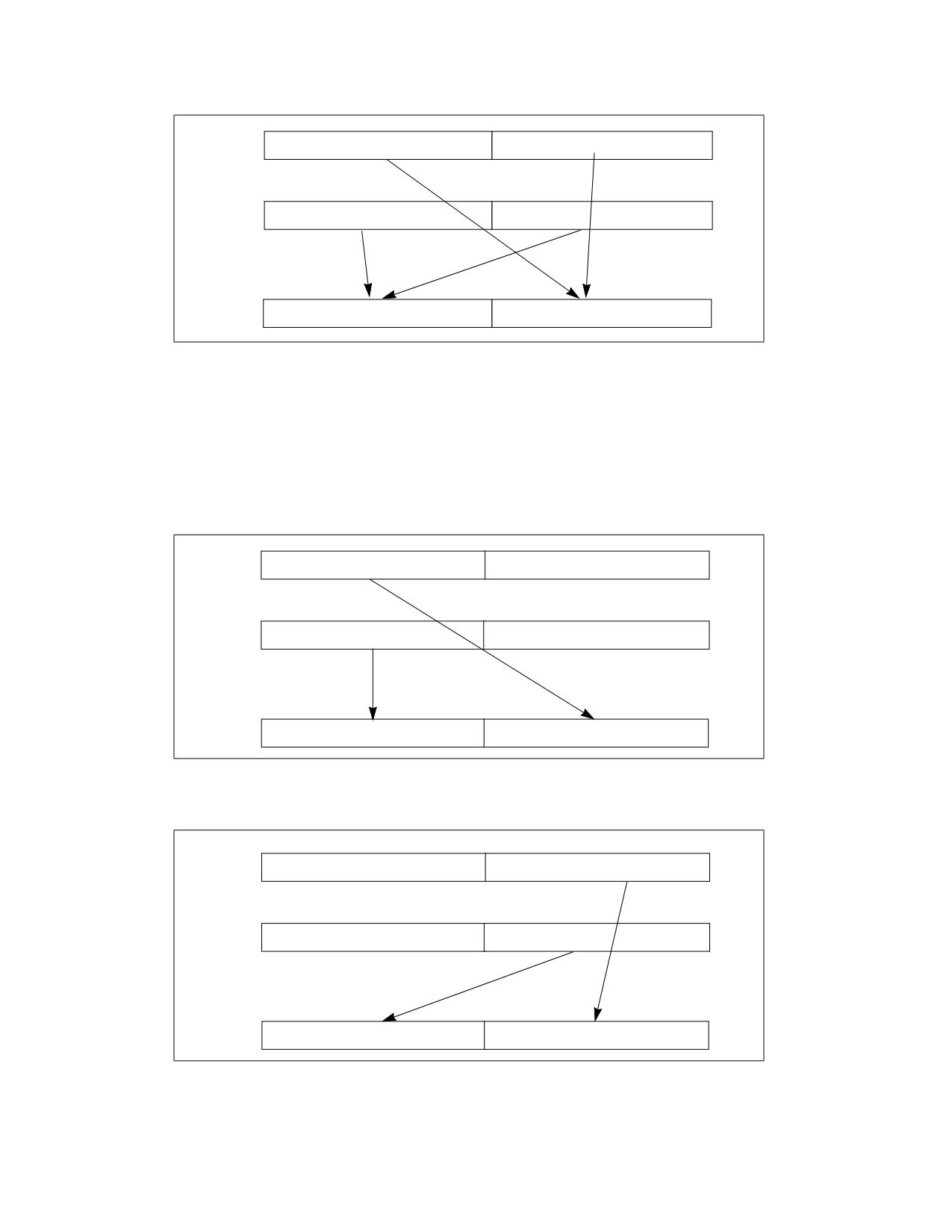
The SHUFPD (shuffle packed double precision floating-point values) instruction places either of the two packed
double precision floating-point values from the destination operand in the low quadword of the destination
operand, and places either of the two packed double precision floating-point values from source operand in the
high quadword of the destination operand (see Figure 11-5). By using the same register for the source and desti-
nation operands, the SHUFPD instruction can swap two packed double precision floating-point values.
Vol. 1
11-7
PROGRAMMING WITH INTEL® STREAMING SIMD EXTENSIONS 2 (INTEL® SSE2)
DEST
X1
X0
SRC
Y1
Y0
DEST
Y1 or Y0
X1 or X0
Figure 11-5. SHUFPD Instruction, Packed Shuffle Operation
The UNPCKHPD (unpack and interleave high packed double precision floating-point values) instruction performs an
interleaved unpack of the high values from the source and destination operands and stores the result in the desti-
nation operand (see Figure 11-6).
The UNPCKLPD (unpack and interleave low packed double precision floating-point values) instruction performs an
interleaved unpack of the low values from the source and destination operands and stores the result in the desti-
nation operand (see Figure 11-7).
DEST
X1
X0
SRC
Y1
Y0
DEST
Y1
X1
Figure 11-6. UNPCKHPD Instruction, High Unpack, and Interleave Operation
DEST
X1
X0
SRC
Y1
Y0
DEST
Y0
X0
Figure 11-7. UNPCKLPD Instruction, Low Unpack, and Interleave Operation
11-8
Vol. 1
PROGRAMMING WITH INTEL® STREAMING SIMD EXTENSIONS 2 (INTEL® SSE2)
11.4.1.6 Intel® SSE2 Conversion Instructions
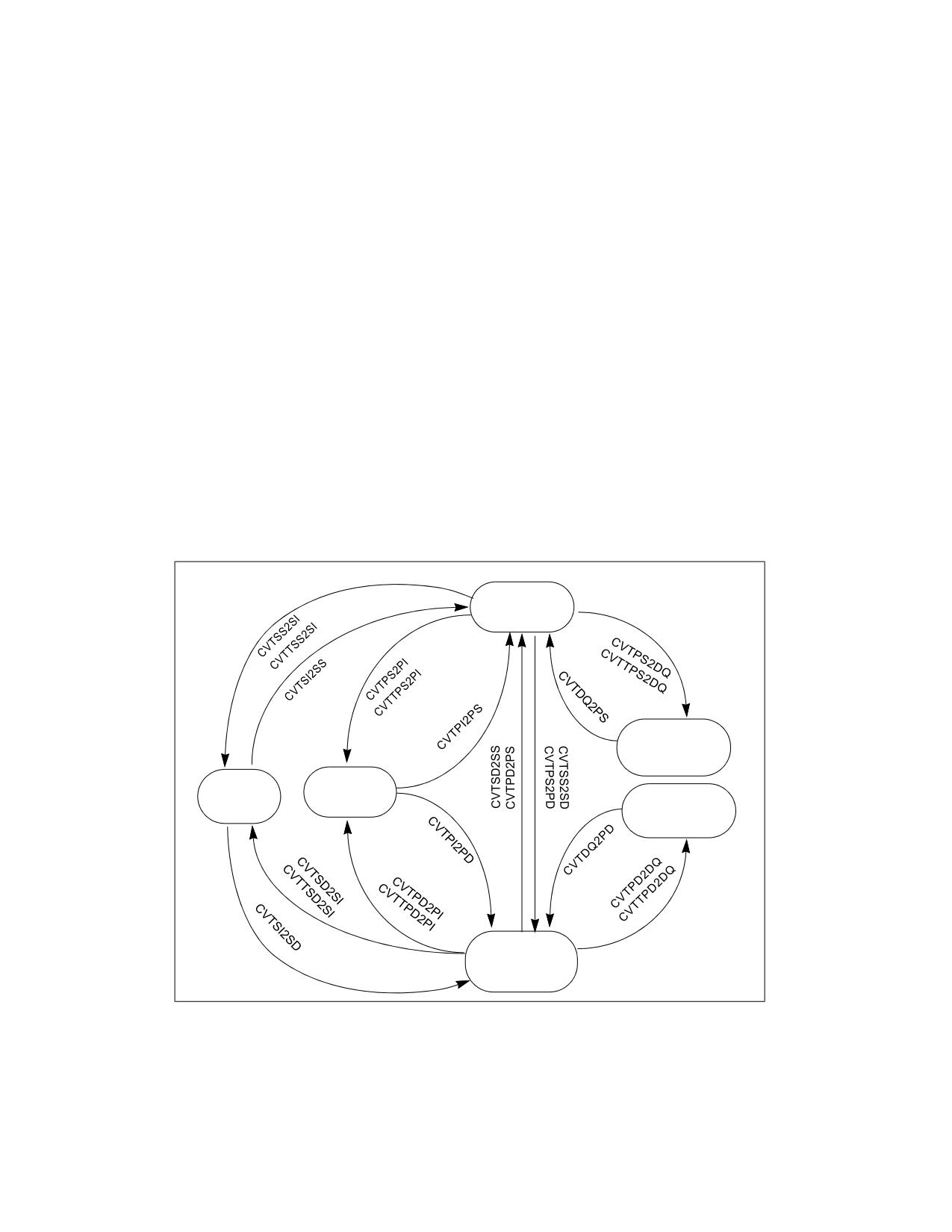
Intel SSE2 conversion instructions (see Figure 11-8) support packed and scalar conversions between:
• Double precision and single precision floating-point formats.
• Double precision floating-point and doubleword integer formats.
• Single precision floating-point and doubleword integer formats.
Conversion between double precision and single precision floating-points values - The following instruc-
tions convert operands between double precision and single precision floating-point formats. The operands being
operated on are contained in XMM registers or memory (at most, one operand can reside in memory; the destina-
tion is always an MMX register).
The CVTPS2PD (convert packed single precision floating-point values to packed double precision floating-point
values) instruction converts two packed single precision floating-point values to two double precision floating-point
values.
The CVTPD2PS (convert packed double precision floating-point values to packed single precision floating-point
values) instruction converts two packed double precision floating-point values to two single precision floating-point
values. When a conversion is inexact, the result is rounded according to the rounding mode selected in the MXCSR
register.
The CVTSS2SD (convert scalar single precision floating-point value to scalar double precision floating-point value)
instruction converts a single precision floating-point value to a double precision floating-point value.
The CVTSD2SS (convert scalar double precision floating-point value to scalar single precision floating-point value)
instruction converts a double precision floating-point value to a single precision floating-point value. When the
conversion is inexact, the result is rounded according to the rounding mode selected in the MXCSR register.
Single Precision
Floating-Point
(XMM/mem)
4 Doubleword
Integer
(XMM/mem)
Doubleword
2 Doubleword
Integer
Integer
2 Doubleword
(r32/mem)
(MMX/mem)
Integer
(XMM/mem)
Double Precision
Floating-Point
(XMM/mem)
Figure 11-8. Intel® SSE and SSE2 Conversion Instructions
Conversion between double precision floating-point values and doubleword integers - The following
instructions convert operands between double precision floating-point and doubleword integer formats. Operands
Vol. 1
11-9
PROGRAMMING WITH INTEL® STREAMING SIMD EXTENSIONS 2 (INTEL® SSE2)
are housed in XMM registers, MMX registers, general registers or memory (at most one operand can reside in
memory; the destination is always an XMM, MMX, or general register).
The CVTPD2PI (convert packed double precision floating-point values to packed doubleword integers) instruction
converts two packed double precision floating-point numbers to two packed signed doubleword integers, with the
result stored in an MMX register. When rounding to an integer value, the source value is rounded according to the
rounding mode in the MXCSR register. The CVTTPD2PI (convert with truncation packed double precision floating-
point values to packed doubleword integers) instruction is similar to the CVTPD2PI instruction except that trunca-
tion is used to round a source value to an integer value; see Section 4.8.4.2, “Truncation with Intel® SSE, SSE2,
and AVX Conversion Instructions.”
The CVTPI2PD (convert packed doubleword integers to packed double precision floating-point values) instruction
converts two packed signed doubleword integers to two double precision floating-point values.
The CVTPD2DQ (convert packed double precision floating-point values to packed doubleword integers) instruction
converts two packed double precision floating-point numbers to two packed signed doubleword integers, with the
result stored in the low quadword of an XMM register. When rounding an integer value, the source value is rounded
according to the rounding mode selected in the MXCSR register. The CVTTPD2DQ (convert with truncation packed
double precision floating-point values to packed doubleword integers) instruction is similar to the CVTPD2DQ
instruction except that truncation is used to round a source value to an integer value; see Section 4.8.4.2, “Trun-
cation with Intel® SSE, SSE2, and AVX Conversion Instructions.”
The CVTDQ2PD (convert packed doubleword integers to packed double precision floating-point values) instruction
converts two packed signed doubleword integers located in the low-order doublewords of an XMM register to two
double precision floating-point values.
The CVTSD2SI (convert scalar double precision floating-point value to signed integer) instruction converts a double
precision floating-point value to a signed integer, and stores the result in a general-purpose register. When
rounding an integer value, the source value is rounded according to the rounding mode selected in the MXCSR
register. The CVTTSD2SI (convert with truncation scalar double precision floating-point value to signed integer)
instruction is similar to the CVTSD2SI instruction except that truncation is used to round the source value to an
integer value; see Section 4.8.4.2, “Truncation with Intel® SSE, SSE2, and AVX Conversion Instructions.”
The CVTSI2SD (convert signed integer to scalar double precision floating-point value) instruction converts a signed
doubleword or quadword integer in a general-purpose register to a double precision floating-point number, and
stores the result in an XMM register.
Conversion between single precision floating-point and doubleword integer formats - These instruc-
tions convert between packed single precision floating-point and packed doubleword integer formats. Operands are
housed in XMM registers, MMX registers, general registers, or memory (the latter for at most one source operand).
The destination is always an XMM, MMX, or general register. These SSE2 instructions supplement conversion
instructions (CVTPI2PS, CVTPS2PI, CVTTPS2PI, CVTSI2SS, CVTSS2SI, and CVTTSS2SI) introduced with Intel SSE
extensions.
The CVTPS2DQ (convert packed single precision floating-point values to packed doubleword integers) instruction
converts four packed single precision floating-point values to four packed signed doubleword integers, with the
source and destination operands in XMM registers or memory (the latter for at most one source operand). When
the conversion is inexact, the rounded value according to the rounding mode selected in the MXCSR register is
returned. The CVTTPS2DQ (convert with truncation packed single precision floating-point values to packed double-
word integers) instruction is similar to the CVTPS2DQ instruction except that truncation is used to round a source
value to an integer value; see Section 4.8.4.2, “Truncation with Intel® SSE, SSE2, and AVX Conversion Instruc-
tions.”
The CVTDQ2PS (convert packed doubleword integers to packed single precision floating-point values) instruction
converts four packed signed doubleword integers to four packed single precision floating-point numbers, with the
source and destination operands in XMM registers or memory (the latter for at most one source operand). When
the conversion is inexact, the rounded value according to the rounding mode selected in the MXCSR register is
returned.
11-10
Vol. 1
PROGRAMMING WITH INTEL® STREAMING SIMD EXTENSIONS 2 (INTEL® SSE2)
11.4.2 Intel® SSE2 64-Bit and 128-Bit SIMD Integer Instructions
Intel SSE2 adds several 128-bit packed integer instructions to the IA-32 architecture. Where appropriate, a 64-bit
version of each of these instructions is also provided. The 128-bit versions of instructions operate on data in XMM
registers; 64-bit versions operate on data in MMX registers. The instructions follow.
The MOVDQA (move aligned double quadword) instruction transfers a double quadword operand from memory to
an XMM register or vice versa; or between XMM registers. The memory address must be aligned to a 16-byte
boundary; otherwise, a general-protection exception (#GP) is generated.
The MOVDQU (move unaligned double quadword) instruction performs the same operations as the MOVDQA
instruction, except that 16-byte alignment of a memory address is not required.
The PADDQ (packed quadword add) instruction adds two packed quadword integer operands or two single quad-
word integer operands, and stores the results in an XMM or MMX register, respectively. This instruction can operate
on either unsigned or signed (two’s complement notation) integer operands.
The PSUBQ (packed quadword subtract) instruction subtracts two packed quadword integer operands or two single
quadword integer operands, and stores the results in an XMM or MMX register, respectively. Like the PADDQ
instruction, PSUBQ can operate on either unsigned or signed (two’s complement notation) integer operands.
The PMULUDQ (multiply packed unsigned doubleword integers) instruction performs an unsigned multiply of
unsigned doubleword integers and returns a quadword result. Both 64-bit and 128-bit versions of this instruction
are available. The 64-bit version operates on two doubleword integers stored in the low doubleword of each source
operand, and the quadword result is returned to an MMX register. The 128-bit version performs a packed multiply
of two pairs of doubleword integers. Here, the doublewords are packed in the first and third doublewords of the
source operands, and the quadword results are stored in the low and high quadwords of an XMM register.
The PSHUFLW (shuffle packed low words) instruction shuffles the word integers packed into the low quadword of
the source operand and stores the shuffled result in the low quadword of the destination operand. An 8-bit imme-
diate operand specifies the shuffle order.
The PSHUFHW (shuffle packed high words) instruction shuffles the word integers packed into the high quadword of
the source operand and stores the shuffled result in the high quadword of the destination operand. An 8-bit imme-
diate operand specifies the shuffle order.
The PSHUFD (shuffle packed doubleword integers) instruction shuffles the doubleword integers packed into the
source operand and stores the shuffled result in the destination operand. An 8-bit immediate operand specifies the
shuffle order.
The PSLLDQ (shift double quadword left logical) instruction shifts the contents of the source operand to the left by
the amount of bytes specified by an immediate operand. The empty low-order bytes are cleared (set to 0).
The PSRLDQ (shift double quadword right logical) instruction shifts the contents of the source operand to the right
by the amount of bytes specified by an immediate operand. The empty high-order bytes are cleared (set to 0).
The PUNPCKHQDQ (Unpack high quadwords) instruction interleaves the high quadword of the source operand and
the high quadword of the destination operand and writes them to the destination register.
The PUNPCKLQDQ (Unpack low quadwords) instruction interleaves the low quadwords of the source operand and
the low quadwords of the destination operand and writes them to the destination register.
Two additional SSE instructions enable data movement from the MMX registers to the XMM registers.
The MOVQ2DQ (move quadword integer from MMX to XMM registers) instruction moves the quadword integer from
an MMX source register to an XMM destination register.
The MOVDQ2Q (move quadword integer from XMM to MMX registers) instruction moves the low quadword integer
from an XMM source register to an MMX destination register.
11.4.3
128-Bit SIMD Integer Instruction Extensions
All of 64-bit SIMD integer instructions introduced with MMX technology and Intel SSE (with the exception of the
PSHUFW instruction) have been extended by Intel SSE2 to operate on 128-bit packed integer operands located in
XMM registers. The 128-bit versions of these instructions follow the same SIMD conventions regarding packed
Vol. 1
11-11
PROGRAMMING WITH INTEL® STREAMING SIMD EXTENSIONS 2 (INTEL® SSE2)
operands as the 64-bit versions. For example, where the 64-bit version of the PADDB instruction operates on 8
packed bytes, the 128-bit version operates on 16 packed bytes.
11.4.4 Cacheability Control and Memory Ordering Instructions
Intel SSE2 instructions that give programs more control over the caching, loading, and storing of data. are
described below.
11.4.4.1 FLUSH Cache Line
The CLFLUSH (flush cache line) instruction writes and invalidates the cache line associated with a specified linear
address. The invalidation is for all levels of the processor’s cache hierarchy, and it is broadcast throughout the
cache coherency domain.
NOTE
CLFLUSH was introduced with Intel SSE2. However, the instruction can be implemented in IA-32
processors that do not implement Intel SSE2. Detect CLFLUSH using the feature bit (if
CPUID.01H:EDX.CLFLUSH[19] = 1).
11.4.4.2 Cacheability Control Instructions
The following four instructions enable data from XMM and general-purpose registers to be stored to memory using
a non-temporal hint. The non-temporal hint directs the processor to store data to memory without writing the data
into the cache hierarchy. See Section 10.4.6.2, “Caching of Temporal vs. Non-Temporal Data,” for more information
about non-temporal stores and hints.
The MOVNTDQ (store double quadword using non-temporal hint) instruction stores packed integer data from an
XMM register to memory, using a non-temporal hint.
The MOVNTPD (store packed double precision floating-point values using non-temporal hint) instruction stores
packed double precision floating-point data from an XMM register to memory, using a non-temporal hint.
The MOVNTI (store doubleword using non-temporal hint) instruction stores integer data from a general-purpose
register to memory, using a non-temporal hint.
The MASKMOVDQU (store selected bytes of double quadword) instruction stores selected byte integers from an
XMM register to memory, using a byte mask to selectively write the individual bytes. The memory location does not
need to be aligned on a natural boundary. This instruction also uses a non-temporal hint.
11.4.4.3 Memory Ordering Instructions
Intel SSE2 introduced two fence instructions (LFENCE and MFENCE) as companions to the SFENCE instruction
introduced with Intel SSE.
The LFENCE instruction establishes a memory fence for loads. It guarantees ordering between two loads and
prevents speculative loads from passing the load fence (that is, no speculative loads are allowed until all loads
specified before the load fence have been carried out).
The MFENCE instruction establishes a memory fence for both loads and stores. The processor ensures that no load
or store after MFENCE will become globally visible until all loads and stores before MFENCE are globally visible.1
Note that the sequences LFENCE;SFENCE and SFENCE;LFENCE are not equivalent to MFENCE because neither
ensures that older stores are globally observed prior to younger loads.
11.4.4.4 Pause
The PAUSE instruction is provided to improve the performance of “spin-wait loops” executed on a Pentium 4 or Intel
Xeon processor. On a Pentium 4 processor, it also provides the added benefit of reducing processor power
1. A load is considered to become globally visible when the value to be loaded is determined.
11-12
Vol. 1
PROGRAMMING WITH INTEL® STREAMING SIMD EXTENSIONS 2 (INTEL® SSE2)
consumption while executing a spin-wait loop. It is recommended that a PAUSE instruction always be included in
the code sequence for a spin-wait loop.
11.4.5 Branch Hints
Intel SSE2 designates two instruction prefixes (2EH and 3EH) to provide branch hints to the processor (see
“Instruction Prefixes” in Chapter 2 of the Intel® 64 and IA-32 Architectures Software Developer’s Manual, Volume
2A). These prefixes can only be used with the Jcc instruction and only at the machine code level (that is, there are
no mnemonics for the branch hints).
11.5
INTEL® SSE, SSE2, AND SSE3 EXCEPTIONS
Intel SSE, SSE2, and SSE3 instructions generate two general types of exceptions:
• Non-numeric exceptions.
• SIMD floating-point exceptions.1
Intel SSE, SSE2, and SSE3 instructions can generate the same type of memory-access and non-numeric excep-
tions as other IA-32 architecture instructions. Existing exception handlers can generally handle these exceptions
without any code modification. See “Providing Non-Numeric Exception Handlers for Exceptions Generated by the
SSE, SSE2, and SSE3 Instructions” in Chapter 16 of the Intel® 64 and IA-32 Architectures Software Developer’s
Manual, Volume 3A, for a list of the non-numeric exceptions that can be generated by the Intel SSE, SSE2, SSE3
instructions and for guidelines for handling these exceptions.
Intel SSE, SSE2, and SSE3 instructions do not generate numeric exceptions on packed integer operations;
however, they can generate numeric (SIMD floating-point) exceptions on packed single precision and double preci-
sion floating-point operations. These SIMD floating-point exceptions are defined in the IEEE Standard 754 for
Floating-Point Arithmetic and are the same exceptions that are generated for x87 FPU instructions. See Section
11.5.1, “SIMD Floating-Point Exceptions,” for a description of these exceptions.
11.5.1 SIMD Floating-Point Exceptions
SIMD floating-point exceptions are those exceptions that can be generated by Intel SSE, SSE2, and SSE3 instruc-
tions that operate on packed or scalar floating-point operands.
Six classes of SIMD floating-point exceptions can be generated:
• Invalid operation (#I).
• Divide-by-zero (#Z).
• Denormal operand (#D).
• Numeric overflow (#O).
• Numeric underflow (#U).
• Inexact result (Precision) (#P).
All of these exceptions (except the denormal operand exception) are defined in IEEE Standard 754, and they are
the same exceptions that are generated with the x87 floating-point instructions. Section 4.9, “Overview of
Floating-Point Exceptions,” gives a detailed description of these exceptions and of how and when they are gener-
ated. The following sections discuss the implementation of these exceptions in the Intel SSE/SSE2/SSE3 exten-
sions.
All SIMD floating-point exceptions are precise and occur as soon as the instruction completes execution.
1. The FISTTP instruction in Intel SSE3 does not generate SIMD floating-point exceptions, but it can generate x87 FPU floating-point
exceptions.
Vol. 1
11-13

PROGRAMMING WITH INTEL® STREAMING SIMD EXTENSIONS 2 (INTEL® SSE2)
Each of the six exception conditions has a corresponding flag (IE, DE, ZE, OE, UE, and PE) and mask bit (IM, DM,
ZM, OM, UM, and PM) in the MXCSR register (see Figure 10-3). The mask bits can be set with the LDMXCSR or
FXRSTOR instruction; the mask and flag bits can be read with the STMXCSR or FXSAVE instruction.
The OSXMMEXCEPT flag (bit 10) of control register CR4 provides additional control over generation of SIMD
floating-point exceptions by allowing the operating system to indicate whether or not it supports software excep-
tion handlers for SIMD floating-point exceptions. If an unmasked SIMD floating-point exception is generated and
the OSXMMEXCEPT flag is set, the processor invokes a software exception handler by generating a SIMD floating-
point exception (#XM). If the OSXMMEXCEPT bit is clear, the processor generates an invalid-opcode exception
(#UD) on the first Intel SSE or SSE2 instruction that detects a SIMD floating-point exception condition. See Section
11.6.2, “Checking for Intel® SSE and SSE2 Support.”
11.5.2 SIMD Floating-Point Exception Conditions
The following sections describe the conditions that cause a SIMD floating-point exception to be generated and the
masked response of the processor when these conditions are detected.
See Section 4.9.2, “Floating-Point Exception Priority,” for a description of the rules for exception precedence when
more than one floating-point exception condition is detected for an instruction.
11.5.2.1 Invalid Operation Exception (#I)
The floating-point invalid-operation exception (#I) occurs in response to an invalid arithmetic operand. The flag
(IE) and mask (IM) bits for the invalid operation exception are bits 0 and 7, respectively, in the MXCSR register.
If the invalid-operation exception is masked, the processor returns a QNaN, QNaN floating-point indefinite, integer
indefinite, one of the source operands to the destination operand, or it sets the EFLAGS, depending on the operation
being performed. When a value is returned to the destination operand, it overwrites the destination register specified
by the instruction. Table 11-1 lists the invalid-arithmetic operations that the processor detects for instructions and
the masked responses to these operations.
Table 11-1. Masked Responses of Intel® SSE, SSE2, and SSE3 Instructions to Invalid Arithmetic Operations
Condition
Masked Response
ADDPS, ADDSS, ADDPD, ADDSD, SUBPS, SUBSS, SUBPD, SUBSD,
Return the SNaN converted to a QNaN; Refer to Table 4-8 for
MULPS, MULSS, MULPD, MULSD, DIVPS, DIVSS, DIVPD, DIVSD,
more details.
ADDSUBPD, ADDSUBPD, HADDPD, HADDPS, HSUBPD or HSUBPS
instruction with an SNaN operand
SQRTPS, SQRTSS, SQRTPD, or SQRTSD with SNaN operands
Return the SNaN converted to a QNaN.
SQRTPS, SQRTSS, SQRTPD, or SQRTSD with negative operands
Return the QNaN floating-point Indefinite.
(except zero)
MAXPS, MAXSS, MAXPD, MAXSD, MINPS, MINSS, MINPD, or
Return the source 2 operand value.
MINSD instruction with QNaN or SNaN operands
CMPPS, CMPSS, CMPPD or CMPSD instruction with QNaN or SNaN
Return a mask of all 0s (except for the predicates “not-equal,”
operands
“unordered,” “not-less-than,” or “not-less-than-or-equal,” which
returns a mask of all 1s).
CVTPD2PS, CVTSD2SS, CVTPS2PD, CVTSS2SD with SNaN
Return the SNaN converted to a QNaN.
operands
COMISS or COMISD with QNaN or SNaN operand(s)
Set EFLAGS values to “not comparable.”
Addition of opposite signed infinities or subtraction of like-signed
Return the QNaN floating-point Indefinite.
infinities
Multiplication of infinity by zero
Return the QNaN floating-point Indefinite.
Divide of (0/0) or ( ∞ / ∞ )
Return the QNaN floating-point Indefinite.
11-14
Vol. 1

PROGRAMMING WITH INTEL® STREAMING SIMD EXTENSIONS 2 (INTEL® SSE2)
Table 11-1. Masked Responses of Intel® SSE, SSE2, and SSE3 Instructions to Invalid Arithmetic Operations (Contd.)
Condition
Masked Response
Conversion to integer when the value in the source register is a
Return the integer Indefinite.
NaN, ∞, or exceeds the representable range for CVTPS2PI,
CVTTPS2PI, CVTSS2SI, CVTTSS2SI, CVTPD2PI, CVTSD2SI,
CVTPD2DQ, CVTTPD2PI, CVTTSD2SI, CVTTPD2DQ, CVTPS2DQ,
or CVTTPS2DQ
If the invalid operation exception is not masked, a software exception handler is invoked and the operands remain
unchanged. See Section 11.5.4, “Handling SIMD Floating-Point Exceptions in Software.”
Normally, when one or more of the source operands are QNaNs (and neither is an SNaN or in an unsupported
format), an invalid-operation exception is not generated. The following instructions are exceptions to this rule: the
COMISS and COMISD instructions; and the CMPPS, CMPSS, CMPPD, and CMPSD instructions (when the predicate
is less than, less-than or equal, not less-than, or not less-than or equal). With these instructions, a QNaN source
operand will generate an invalid-operation exception.
The invalid-operation exception is not affected by the flush-to-zero mode or by the denormals-are-zeros mode.
11.5.2.2 Denormal-Operand Exception (#D)
The processor signals the denormal-operand exception if an arithmetic instruction attempts to operate on a
denormal operand. The flag (DE) and mask (DM) bits for the denormal-operand exception are bits 1 and 8, respec-
tively, in the MXCSR register.
The CVTPI2PD, CVTPD2PI, CVTTPD2PI, CVTDQ2PD, CVTPD2DQ, CVTTPD2DQ, CVTSI2SD, CVTSD2SI, CVTTSD2SI,
CVTPI2PS, CVTPS2PI, CVTTPS2PI, CVTSS2SI, CVTTSS2SI, CVTSI2SS, CVTDQ2PS, CVTPS2DQ, and CVTTPS2DQ
conversion instructions do not signal denormal exceptions. The RCPSS, RCPPS, RSQRTSS, and RSQRTPS instruc-
tions do not signal any kind of floating-point exception.
The denormals-are-zero flag (bit 6) of the MXCSR register provides an additional option for handling denormal-
operand exceptions. When this flag is set, denormal source operands are automatically converted to zeros with the
sign of the source operand (see Section 10.2.3.4, “Denormals-Are-Zeros”). The denormal operand exception is not
affected by the flush-to-zero mode.
See Section 4.9.1.2, “Denormal Operand Exception (#D),” for more information about the denormal exception.
See Section 11.5.4, “Handling SIMD Floating-Point Exceptions in Software,” for information on handling unmasked
exceptions.
11.5.2.3 Divide-By-Zero Exception (#Z)
The processor reports a divide-by-zero exception when a DIVPS, DIVSS, DIVPD or DIVSD instruction attempts to
divide a finite non-zero operand by 0. The flag (ZE) and mask (ZM) bits for the divide-by-zero exception are bits 2
and 9, respectively, in the MXCSR register.
See Section 4.9.1.3, “Divide-By-Zero Exception (#Z),” for more information about the divide-by-zero exception.
See Section 11.5.4, “Handling SIMD Floating-Point Exceptions in Software,” for information on handling unmasked
exceptions.
The divide-by-zero exception is not affected by the flush-to-zero mode at a single-instruction boundary.
While DAZ does not affect the rules for signaling IEEE exceptions, operations on denormal inputs might have
different results when DAZ=1. As a consequence, DAZ can have an effect on the floating-point exceptions -
including the divide-by-zero exception - when observed for a given operation involving denormal inputs.
11.5.2.4 Numeric Overflow Exception (#O)
The processor reports a numeric overflow exception whenever the rounded result of an arithmetic instruction
exceeds the largest allowable finite value that fits in the destination operand. This exception can be generated with
the ADDPS, ADDSS, ADDPD, ADDSD, SUBPS, SUBSS, SUBPD, SUBSD, MULPS, MULSS, MULPD, MULSD, DIVPS,
DIVSS, DIVPD, DIVSD, CVTPD2PS, CVTSD2SS, ADDSUBPD, ADDSUBPS, HADDPD, HADDPS, HSUBPD, and
Vol. 1
11-15
PROGRAMMING WITH INTEL® STREAMING SIMD EXTENSIONS 2 (INTEL® SSE2)
HSUBPS instructions. The flag (OE) and mask (OM) bits for the numeric overflow exception are bits 3 and 10,
respectively, in the MXCSR register.
See Section 4.9.1.4, “Numeric Overflow Exception (#O),” for more information about the numeric-overflow excep-
tion. See Section 11.5.4, “Handling SIMD Floating-Point Exceptions in Software,” for information on handling
unmasked exceptions.
The numeric overflow exception is not affected by the flush-to-zero mode or by the denormals-are-zeros mode.
11.5.2.5 Numeric Underflow Exception (#U)
The processor reports a numeric underflow exception whenever the magnitude of the rounded result of an arith-
metic instruction, with unbounded exponent, is less than the smallest possible normalized, finite value that will fit
in the destination operand and the numeric-underflow exception is not masked. If the numeric underflow exception
is masked, both underflow and the inexact-result condition must be detected before numeric underflow is reported.
This exception can be generated with the ADDPS, ADDSS, ADDPD, ADDSD, SUBPS, SUBSS, SUBPD, SUBSD,
MULPS, MULSS, MULPD, MULSD, DIVPS, DIVSS, DIVPD, DIVSD, CVTPD2PS, CVTSD2SS, ADDSUBPD, ADDSUBPS,
HADDPD, HADDPS, HSUBPD, and HSUBPS instructions. The flag (UE) and mask (UM) bits for the numeric under-
flow exception are bits 4 and 11, respectively, in the MXCSR register.
The flush-to-zero flag (bit 15) of the MXCSR register provides an additional option for handling numeric underflow
exceptions. When this flag is set and the numeric underflow exception is masked, tiny results are returned as a zero
with the sign of the true result; see Section 10.2.3.3, “Flush-To-Zero.”
Underflow will occur when a tiny non-zero result is detected (the result has to be also inexact if underflow excep-
tions are masked), as described in the IEEE Standard 754-2008. While DAZ does not affect the rules for signaling
IEEE exceptions, operations on denormal inputs might have different results when DAZ=1. As a consequence, DAZ
can have an effect on the floating-point exceptions - including the underflow exception - when observed for a given
operation involving denormal inputs.
See Section 4.9.1.5, “Numeric Underflow Exception (#U),” for more information about the numeric underflow
exception. See Section 11.5.4, “Handling SIMD Floating-Point Exceptions in Software,” for information on handling
unmasked exceptions.
11.5.2.6 Inexact-Result (Precision) Exception (#P)
The inexact-result exception (also called the precision exception) occurs if the result of an operation is not exactly
representable in the destination format. For example, the fraction 1/3 cannot be precisely represented in binary
form. This exception occurs frequently and indicates that some (normally acceptable) accuracy has been lost. The
exception is supported for applications that need to perform exact arithmetic only. Because the rounded result is
generally satisfactory for most applications, this exception is commonly masked.
The flag (PE) and mask (PM) bits for the inexact-result exception are bits 5 and 12, respectively, in the MXCSR
register.
See Section 4.9.1.6, “Inexact-Result (Precision) Exception (#P),” for more information about the inexact-result
exception. See Section 11.5.4, “Handling SIMD Floating-Point Exceptions in Software,” for information on handling
unmasked exceptions.
In flush-to-zero mode, the inexact result exception is reported.
11.5.3 Generating SIMD Floating-Point Exceptions
When the processor executes a packed or scalar floating-point instruction, it looks for and reports on SIMD
floating-point exception conditions using two sequential steps:
1. Looks for, reports on, and handles pre-computation exception conditions (invalid-operand, divide-by-zero, and
denormal operand)
2. Looks for, reports on, and handles post-computation exception conditions (numeric overflow, numeric
underflow, and inexact result)
11-16
Vol. 1
PROGRAMMING WITH INTEL® STREAMING SIMD EXTENSIONS 2 (INTEL® SSE2)
If both pre- and post-computational exceptions are unmasked, it is possible for the processor to generate a SIMD
floating-point exception (#XM) twice during the execution of an SSE, SSE2 or SSE3 instruction: once when it
detects and handles a pre-computational exception and when it detects a post-computational exception.
11.5.3.1 Handling Masked Exceptions
If all exceptions are masked, the processor handles the exceptions it detects by placing the masked result (or
results for packed operands) in a destination operand and continuing program execution. The masked result may
be a rounded normalized value, signed infinity, a denormal finite number, zero, a QNaN floating-point indefinite, or
a QNaN depending on the exception condition detected. In most cases, the corresponding exception flag bit in
MXCSR is also set. The one situation where an exception flag is not set is when an underflow condition is detected
and it is not accompanied by an inexact result.
When operating on packed floating-point operands, the processor returns a masked result for each of the sub-
operand computations and sets a separate set of internal exception flags for each computation. It then performs a
logical-OR on the internal exception flag settings and sets the exception flags in the MXCSR register according to
the results of OR operations.
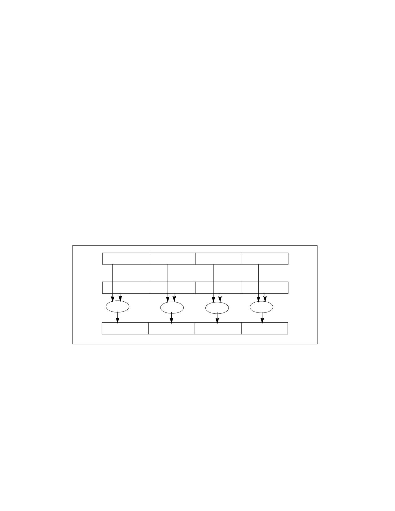
For example, Figure 11-9 shows the results of an MULPS instruction. In the example, all SIMD floating-point excep-
tions are masked. Assume that a denormal exception condition is detected prior to the multiplication of sub-oper-
ands X0 and Y0, no exception condition is detected for the multiplication of X1 and Y1, a numeric overflow
exception condition is detected for the multiplication of X2 and Y2, and another denormal exception is detected
prior to the multiplication of sub-operands X3 and Y3. Because denormal exceptions are masked, the processor
uses the denormal source values in the multiplications of (X0 and Y0) and of (X3 and Y3) passing the results of the
multiplications through to the destination operand. With the denormal operand, the result of the X0 and Y0 compu-
tation is a normalized finite value, with no exceptions detected. However, the X3 and Y3 computation produces a
tiny and inexact result. This causes the corresponding internal numeric underflow and inexact-result exception
flags to be set.
X3
X2
X1
X0 (Denormal)
Y3 (Denormal)
Y2
Y1
Y0
MULPS
MULPS
MULPS
MULPS
Tiny, Inexact, Finite
∞
Normalized Finite
Normalized Finite
Figure 11-9. Example Masked Response for Packed Operations
For the multiplication of X2 and Y2, the processor stores the floating-point ∞ in the destination operand, and sets
the corresponding internal sub-operand numeric overflow flag. The result of the X1 and Y1 multiplication is passed
through to the destination operand, with no internal sub-operand exception flags being set. Following the compu-
tations, the individual sub-operand exceptions flags for denormal operand, numeric underflow, inexact result, and
numeric overflow are OR’d and the corresponding flags are set in the MXCSR register.
The net result of this computation is that:
• Multiplication of X0 and Y0 produces a normalized finite result
• Multiplication of X1 and Y1 produces a normalized finite result
• Multiplication of X2 and Y2 produces a floating-point ∞ result
• Multiplication of X3 and Y3 produces a tiny, inexact, finite result
Vol. 1
11-17
PROGRAMMING WITH INTEL® STREAMING SIMD EXTENSIONS 2 (INTEL® SSE2)
• Denormal operand, numeric underflow, numeric underflow, and inexact result flags are set in the MXCSR
register
11.5.3.2 Handling Unmasked Exceptions
If all exceptions are unmasked, the processor:
1. First detects any pre-computation exceptions: it ORs those exceptions, sets the appropriate exception flags,
leaves the source and destination operands unaltered, and goes to step 2. If it does not detect any pre-
computation exceptions, it goes to step 5.
2. Checks CR4.OSXMMEXCPT[bit 10]. If this flag is set, the processor goes to step 3; if the flag is clear, it
generates an invalid-opcode exception (#UD) and makes an implicit call to the invalid-opcode exception
handler.
3. Generates a SIMD floating-point exception (#XM) and makes an implicit call to the SIMD floating-point
exception handler.
4. If the exception handler is able to fix the source operands that generated the pre-computation exceptions or
mask the condition in such a way as to allow the processor to continue executing the instruction, the processor
resumes instruction execution as described in step 5.
5. Upon returning from the exception handler (or if no pre-computation exceptions were detected), the processor
checks for post-computation exceptions. If the processor detects any post-computation exceptions: it ORs
those exceptions, sets the appropriate exception flags, leaves the source and destination operands unaltered,
and repeats steps 2, 3, and 4.
6. Upon returning from the exceptions handler in step 4 (or if no post-computation exceptions were detected), the
processor completes the execution of the instruction.
The implication of this procedure is that for unmasked exceptions, the processor can generate a SIMD floating-
point exception (#XM) twice: once if it detects pre-computation exception conditions and a second time if it detects
post-computation exception conditions. For example, if SIMD floating-point exceptions are unmasked for the
computation shown in Figure 11-9, the processor would generate one SIMD floating-point exception for denormal
operand conditions and a second SIMD floating-point exception for overflow and underflow (no inexact result
exception would be generated because the multiplications of X0 and Y0 and of X1 and Y1 are exact).
11.5.3.3 Handling Combinations of Masked and Unmasked Exceptions
In situations where both masked and unmasked exceptions are detected, the processor will set exception flags for
the masked and the unmasked exceptions. However, it will not return masked results until after the processor has
detected and handled unmasked post-computation exceptions and returned from the exception handler (as in step
6 above) to finish executing the instruction.
11.5.4 Handling SIMD Floating-Point Exceptions in Software
Section 4.9.3, “Typical Actions of a Floating-Point Exception Handler,” shows actions that may be carried out by a
SIMD floating-point exception handler. The SSE/SSE2/SSE3 state is saved with the FXSAVE instruction; see Section
11.6.5, “Saving and Restoring the SSE/SSE2 State.”
11.5.5 Interaction of SIMD and x87 FPU Floating-Point Exceptions
SIMD floating-point exceptions are generated independently from x87 FPU floating-point exceptions. SIMD
floating-point exceptions do not cause assertion of the FERR# pin (independent of the value of CR0.NE[bit 5]).
They ignore the assertion and deassertion of the IGNNE# pin.
If applications use Intel SSE/SSE2/SSE3 instructions along with x87 FPU instructions (in the same task or
program), consider the following:
• SIMD floating-point exceptions are reported independently from the x87 FPU floating-point exceptions. SIMD
and x87 FPU floating-point exceptions can be unmasked independently. Separate x87 FPU and SIMD floating-
11-18
Vol. 1
PROGRAMMING WITH INTEL® STREAMING SIMD EXTENSIONS 2 (INTEL® SSE2)
point exception handlers must be provided if the same exception is unmasked for x87 FPU and for Intel
SSE/SSE2/SSE3 operations.
• The rounding mode specified in the MXCSR register does not affect x87 FPU instructions. Likewise, the
rounding mode specified in the x87 FPU control word does not affect the Intel SSE/SSE2/SSE3 instructions. To
use the same rounding mode, the rounding control bits in the MXCSR register and in the x87 FPU control word
must be set explicitly to the same value.
• The flush-to-zero mode set in the MXCSR register for Intel SSE/SSE2/SSE3 instructions has no counterpart in
the x87 FPU. For compatibility with the x87 FPU, set the flush-to-zero bit to 0.
• The denormals-are-zeros mode set in the MXCSR register for Intel SSE/SSE2/SSE3 instructions has no
counterpart in the x87 FPU. For compatibility with the x87 FPU, set the denormals-are-zeros bit to 0.
• An application that expects to detect x87 FPU exceptions that occur during the execution of x87 FPU instruc-
tions will not be notified if exceptions occurs during the execution of corresponding Intel SSE/SSE2/SSE31
instructions, unless the exception masks that are enabled in the x87 FPU control word have also been enabled
in the MXCSR register and the application is capable of handling SIMD floating-point exceptions (#XM).
- Masked exceptions that occur during an SSE/SSE2/SSE3 library call cannot be detected by unmasking the
exceptions after the call (in an attempt to generate the fault based on the fact that an exception flag is set).
A SIMD floating-point exception flag that is set when the corresponding exception is unmasked will not
generate a fault; only the next occurrence of that unmasked exception will generate a fault.
- An application which checks the x87 FPU status word to determine if any masked exception flags were set
during an x87 FPU library call will also need to check the MXCSR register to detect a similar occurrence of a
masked exception flag being set during an SSE/SSE2/SSE3 library call.
11.6
WRITING APPLICATIONS WITH INTEL® SSE AND SSE2
The following sections give some guidelines for writing application programs and operating-system code that uses
Intel SSE and SSE2. Because Intel SSE and SSE2 share the same state and perform companion operations, these
guidelines apply to both sets of extensions.
Chapter 16 in the Intel® 64 and IA-32 Architectures Software Developer’s Manual, Volume 3A, discusses the inter-
face to the processor for context switching as well as other operating system considerations when writing code that
uses Intel SSE, SSE2, and SSE3.
11.6.1 General Guidelines for Using Intel® SSE and SSE2
The following guidelines describe how to take full advantage of the performance gains available with Intel SSE and
SSE2:
• Ensure that the processor supports Intel SSE and SSE2.
• Ensure that your operating system supports Intel SSE and SSE2. (Operating system support for Intel SSE
implies support for Intel SSE2, and vice versa.)
• Use stack and data alignment techniques to keep data properly aligned for efficient memory use.
• Use the non-temporal store instructions offered with Intel SSE and SSE2.
• Employ the optimization and scheduling techniques described in the Intel® 64 and IA-32 Architectures Optimi-
zation Reference Manual; see Section 1.4, “Related Literature,” for the order number for this manual.
11.6.2 Checking for Intel® SSE and SSE2 Support
Before an application attempts to use Intel SSE and/or Intel SSE2, it should check that they are present on the
processor:
1. Intel SSE3 refers to ADDSUBPD, ADDSUBPS, HADDPD, HADDPS, HSUBPD, and HSUBPS. The only other Intel SSE3 instruction that
can raise floating-point exceptions is FISTTP; it can generate x87 FPU invalid operation and inexact result exceptions.
Vol. 1
11-19

PROGRAMMING WITH INTEL® STREAMING SIMD EXTENSIONS 2 (INTEL® SSE2)
1. Check that the processor supports the CPUID instruction. Bit 21 of the EFLAGS register can be used to check
processor’s support the CPUID instruction.
2. Check that the processor supports Intel SSE and/or SSE2 (true if CPUID.01H:EDX.SSE[25] = 1 and/or
CPUID.01H:EDX.SSE2[26] = 1).
The operating system must provide system level support for handling SSE state, exceptions before an application
can use Intel SSE and/or Intel SSE2; see Chapter 16 in the Intel® 64 and IA-32 Architectures Software Developer’s
Manual, Volume 3A.
If the processor attempts to execute an unsupported Intel SSE or SSE2 instruction, the processor will generate an
invalid-opcode exception (#UD). If an operating system did not provide adequate system level support for Intel
SSE, executing an Intel SSE or SSE2 instructions can also generate #UD.
11.6.3 Checking for the DAZ Flag in the MXCSR Register
The denormals-are-zero flag in the MXCSR register is available in most of the Pentium 4 processors and in the Intel
Xeon processor, with the exception of some early steppings. To check for the presence of the DAZ flag in the MXCSR
register, do the following:
1. Establish a 512-byte FXSAVE area in memory.
2. Clear the FXSAVE area to all 0s.
3. Execute the FXSAVE instruction, using the address of the first byte of the cleared FXSAVE area as a source
operand. See “FXSAVE-Save x87 FPU, MMX, SSE, and SSE2 State” in Chapter 3 of the Intel® 64 and IA-32
Architectures Software Developer’s Manual, Volume 2A, for a description of the FXSAVE instruction and the
layout of the FXSAVE image.
4. Check the value in the MXCSR_MASK field in the FXSAVE image (bytes 28 through 31).
- If the value of the MXCSR_MASK field is 00000000H, the DAZ flag and denormals-are-zero mode are not
supported.
- If the value of the MXCSR_MASK field is non-zero and bit 6 is set, the DAZ flag and denormals-are-zero
mode are supported.
If the DAZ flag is not supported, then it is a reserved bit and attempting to write a 1 to it will cause a general-
protection exception (#GP). See Section 11.6.6, “Guidelines for Writing to the MXCSR Register,” for general guide-
lines for preventing general-protection exceptions when writing to the MXCSR register.
11.6.4 Initialization of Intel® SSE and SSE2
The SSE and SSE2 state is contained in the XMM and MXCSR registers. Upon a hardware reset of the processor, this
state is initialized as follows (see Table 11-2):
• All SIMD floating-point exceptions are masked (bits 7 through 12 of the MXCSR register is set to 1).
• All SIMD floating-point exception flags are cleared (bits 0 through 5 of the MXCSR register is set to 0).
• The rounding control is set to round-nearest (bits 13 and 14 of the MXCSR register are set to 00B).
• The flush-to-zero mode is disabled (bit 15 of the MXCSR register is set to 0).
• The denormals-are-zeros mode is disabled (bit 6 of the MXCSR register is set to 0). If the denormals-are-zeros
mode is not supported, this bit is reserved and will be set to 0 on initialization.
• Each of the XMM registers is cleared (set to all zeros).
Table 11-2. SSE and SSE2 State Following a Power-up/Reset or INIT
Registers
Power-Up or Reset
INIT
XMM0 through XMM7
+0.0
Unchanged
MXCSR
1F80H
Unchanged
If the processor is reset by asserting the INIT# pin, the SSE and SSE2 state is not changed.
11-20
Vol. 1
PROGRAMMING WITH INTEL® STREAMING SIMD EXTENSIONS 2 (INTEL® SSE2)
11.6.5 Saving and Restoring the SSE/SSE2 State
The FXSAVE instruction saves the x87 FPU, MMX, SSE, and SSE2 states (which includes the contents of eight XMM
registers and the MXCSR registers) in a 512-byte block of memory. The FXRSTOR instruction restores the saved
SSE and SSE2 state from memory. See the FXSAVE instruction in Chapter 3 of the Intel® 64 and IA-32 Architec-
tures Software Developer’s Manual, Volume 2A, for the layout of the 512-byte state block.
In addition to saving and restoring the SSE and SSE2 state, FXSAVE and FXRSTOR also save and restore the x87
FPU state (because MMX registers are aliased to the x87 FPU data registers this includes saving and restoring the
MMX state). For greater code efficiency, it is suggested that FXSAVE and FXRSTOR be substituted for the FSAVE,
FNSAVE, and FRSTOR instructions in the following situations:
• When a context switch is being made in a multitasking environment
• During calls and returns from interrupt and exception handlers
In situations where the code is switching between x87 FPU and MMX technology computations (without a context
switch or a call to an interrupt or exception), the FSAVE/FNSAVE and FRSTOR instructions are more efficient than
the FXSAVE and FXRSTOR instructions.
11.6.6 Guidelines for Writing to the MXCSR Register
The MXCSR has several reserved bits, and attempting to write a 1 to any of these bits will cause a general-protec-
tion exception (#GP) to be generated. To allow software to identify these reserved bits, the MXCSR_MASK value is
provided. Software can determine this mask value as follows:
1. Establish a 512-byte FXSAVE area in memory.
2. Clear the FXSAVE area to all 0s.
3. Execute the FXSAVE instruction, using the address of the first byte of the cleared FXSAVE area as a source
operand. See “FXSAVE-Save x87 FPU, MMX, SSE, and SSE2 State” in Chapter 3 of the Intel® 64 and IA-32
Architectures Software Developer’s Manual, Volume 2A, for a description of FXSAVE and the layout of the
FXSAVE image.
4. Check the value in the MXCSR_MASK field in the FXSAVE image (bytes 28 through 31).
- If the value of the MXCSR_MASK field is 00000000H, then the MXCSR_MASK value is the default value of
0000FFBFH. Note that this value indicates that bit 6 of the MXCSR register is reserved; this setting indicates
that the denormals-are-zero mode is not supported on the processor.
- If the value of the MXCSR_MASK field is non-zero, the MXCSR_MASK value should be used as the
MXCSR_MASK.
All bits set to 0 in the MXCSR_MASK value indicate reserved bits in the MXCSR register. Thus, if the MXCSR_MASK
value is AND’d with a value to be written into the MXCSR register, the resulting value will be assured of having all
its reserved bits set to 0, preventing the possibility of a general-protection exception being generated when the
value is written to the MXCSR register.
For example, the default MXCSR_MASK value when 00000000H is returned in the FXSAVE image is 0000FFBFH. If
software AND’s a value to be written to MXCSR register with 0000FFBFH, bit 6 of the result (the DAZ flag) will be
ensured of being set to 0, which is the required setting to prevent general-protection exceptions on processors that
do not support the denormals-are-zero mode.
To prevent general-protection exceptions, the MXCSR_MASK value should be AND’d with the value to be written
into the MXCSR register in the following situations:
• Operating system routines that receive a parameter from an application program and then write that value to
the MXCSR register (either with an FXRSTOR or LDMXCSR instruction)
• Any application program that writes to the MXCSR register and that needs to run robustly on several different
IA-32 processors
Note that all bits in the MXCSR_MASK value that are set to 1 indicate features that are supported by the MXCSR
register; they can be treated as feature flags for identifying processor capabilities.
Vol. 1
11-21
PROGRAMMING WITH INTEL® STREAMING SIMD EXTENSIONS 2 (INTEL® SSE2)
11.6.7 Interaction of Intel® SSE and SSE2 Instructions with x87 FPU and MMX Instructions
The XMM registers and the x87 FPU and MMX registers represent separate execution environments, which has
certain ramifications when executing Intel SSE, SSE2, MMX, and x87 FPU instructions in the same code module or
when mixing code modules that contain these instructions:
• Those Intel SSE and SSE2 instructions that operate only on XMM registers (such as the packed and scalar
floating-point instructions and the 128-bit SIMD integer instructions) in the same instruction stream with 64-
bit SIMD integer or x87 FPU instructions without any restrictions. For example, an application can perform the
majority of its floating-point computations in the XMM registers, using the packed and scalar floating-point
instructions, and at the same time use the x87 FPU to perform trigonometric and other transcendental compu-
tations. Likewise, an application can perform packed 64-bit and 128-bit SIMD integer operations together
without restrictions.
• Those Intel SSE and SSE2 instructions that operate on MMX registers (such as the CVTPS2PI, CVTTPS2PI,
CVTPI2PS, CVTPD2PI, CVTTPD2PI, CVTPI2PD, MOVDQ2Q, MOVQ2DQ, PADDQ, and PSUBQ instructions) can
also be executed in the same instruction stream as 64-bit SIMD integer or x87 FPU instructions, however, here
they are subject to the restrictions on the simultaneous use of MMX technology and x87 FPU instructions, which
include:
- Transition from x87 FPU to MMX technology instructions or to Intel SSE or SSE2 instructions that operate
on MMX registers should be preceded by saving the state of the x87 FPU.
- Transition from MMX technology instructions or from Intel SSE or SSE2 instructions that operate on MMX
registers to x87 FPU instructions should be preceded by execution of the EMMS instruction.
11.6.8 Compatibility of SIMD and x87 FPU Floating-Point Data Types
Intel SSE and SSE2 instructions operate on the same single precision and double precision floating-point data types
that the x87 FPU operates on. However, when operating on these data types, Intel SSE and SSE2 operate on them
in their native format (single precision or double precision), in contrast to the x87 FPU which extends them to
double extended precision floating-point format to perform computations and then rounds the result back to a
single precision or double precision format before writing results to memory. Because the x87 FPU operates on a
higher precision format and then rounds the result to a lower precision format, it may return a slightly different
result when performing the same operation on the same single precision or double precision floating-point values
than is returned by Intel SSE and SSE2. The difference occurs only in the least-significant bits of the significand.
11.6.9 Mixing Packed and Scalar Floating-Point and 128-Bit SIMD Integer Instructions and
Data
Intel SSE and SSE2 define typed operations on packed and scalar floating-point data types and on 128-bit SIMD
integer data types, but IA-32 processors do not enforce this typing at the architectural level. They only enforce it
at the microarchitectural level. Therefore, when a Pentium 4 or Intel Xeon processor loads a packed or scalar
floating-point operand or a 128-bit packed integer operand from memory into an XMM register, it does not check
that the actual data being loaded matches the data type specified in the instruction. Likewise, when the processor
performs an arithmetic operation on the data in an XMM register, it does not check that the data being operated on
matches the data type specified in the instruction.
As a general rule, because data typing of SIMD floating-point and integer data types is not enforced at the archi-
tectural level, it is the responsibility of the programmer, assembler, or compiler to ensure that code enforces data
typing. Failure to enforce correct data typing can lead to computations that return unexpected results.
For example, in the following code sample, two packed single precision floating-point operands are moved from
memory into XMM registers (using MOVAPS instructions); then a double precision packed add operation (using the
ADDPD instruction) is performed on the operands:
movaps
xmm0, [eax]
; EAX register contains pointer to packed
; single precision floating-point operand
movaps
xmm1, [ebx]
addpd
xmm0, xmm1
11-22
Vol. 1
PROGRAMMING WITH INTEL® STREAMING SIMD EXTENSIONS 2 (INTEL® SSE2)
Pentium 4 and Intel Xeon processors execute these instructions without generating an invalid-operand exception
(#UD) and will produce the expected results in register XMM0 (that is, the high and low 64-bits of each register will
be treated as a double precision floating-point value and the processor will operate on them accordingly). Because
the data types operated on and the data type expected by the ADDPD instruction were inconsistent, the instruction
may result in a SIMD floating-point exception (such as numeric overflow [#O] or invalid operation [#I]) being
generated, but the actual source of the problem (inconsistent data types) is not detected.
The ability to operate on an operand that contains a data type that is inconsistent with the typing of the instruction
being executed, permits some valid operations to be performed. For example, the following instructions load a
packed double precision floating-point operand from memory to register XMM0, and a mask to register XMM1; then
they use XORPD to toggle the sign bits of the two packed values in register XMM0.
movapd
xmm0, [eax]
; EAX register contains pointer to packed
; double precision floating-point operand
movaps
xmm1, [ebx]
; EBX register contains pointer to packed
; double precision floating-point mask
xorpd
xmm0, xmm1
; XOR operation toggles sign bits using
; the mask in xmm1
In this example: XORPS or PXOR can be used in place of XORPD and yield the same correct result. However,
because of the type mismatch between the operand data type and the instruction data type, a latency penalty will
be incurred due to implementations of the instructions at the microarchitecture level.
Latency penalties can also be incurred by using move instructions of the wrong type. For example, MOVAPS and
MOVAPD can both be used to move a packed single precision operand from memory to an XMM register. However,
if MOVAPD is used, a latency penalty will be incurred when a correctly typed instruction attempts to use the data in
the register.
Note that these latency penalties are not incurred when moving data from XMM registers to memory.
11.6.10 Interfacing with Intel® SSE and SSE2 Procedures and Functions
Intel SSE and SSE2 allow direct access to XMM registers. This means that all existing interface conventions
between procedures and functions that apply to the use of the general-purpose registers (EAX, EBX, etc.) also
apply to XMM register usage.
11.6.10.1 Passing Parameters in XMM Registers
The state of XMM registers is preserved across procedure (or function) boundaries. Parameters can be passed from
one procedure to another using XMM registers.
11.6.10.2 Saving XMM Register State on a Procedure or Function Call
The state of XMM registers can be saved in two ways: using an FXSAVE instruction or a move instruction. FXSAVE
saves the state of all XMM registers (along with the state of MXCSR and the x87 FPU registers). This instruction is
typically used for major changes in the context of the execution environment, such as a task switch. FXRSTOR
restores the XMM, MXCSR, and x87 FPU registers stored with FXSAVE.
In cases where only XMM registers must be saved, or where selected XMM registers need to be saved, move
instructions (MOVAPS, MOVUPS, MOVSS, MOVAPD, MOVUPD, MOVSD, MOVDQA, and MOVDQU) can be used.
These instructions can also be used to restore the contents of XMM registers. To avoid performance degradation
when saving XMM registers to memory or when loading XMM registers from memory, be sure to use the appropri-
ately typed move instructions.
The move instructions can also be used to save the contents of XMM registers on the stack. Here, the stack pointer
(in the ESP register) can be used as the memory address to the next available byte in the stack. Note that the stack
pointer is not automatically incremented when using a move instruction (as it is with PUSH).
Vol. 1
11-23
PROGRAMMING WITH INTEL® STREAMING SIMD EXTENSIONS 2 (INTEL® SSE2)
A move-instruction procedure that saves the contents of an XMM register to the stack is responsible for decre-
menting the value in the ESP register by 16. Likewise, a move-instruction procedure that loads an XMM register
from the stack needs also to increment the ESP register by 16. To avoid performance degradation when moving the
contents of XMM registers, use the appropriately typed move instructions.
Use the LDMXCSR and STMXCSR instructions to save and restore, respectively, the contents of the MXCSR register
on a procedure call and return.
11.6.10.3 Caller-Save Recommendation for Procedure and Function Calls
When making procedure (or function) calls from SSE or SSE2 code, a caller-save convention is recommended for
saving the state of the calling procedure. Using this convention, any register whose content must survive intact
across a procedure call must be stored in memory by the calling procedure prior to executing the call.
The primary reason for using the caller-save convention is to prevent performance degradation. XMM registers can
contain packed or scalar double precision floating-point, packed single precision floating-point, and 128-bit packed
integer data types. The called procedure has no way of knowing the data types in XMM registers following a call; so
it is unlikely to use the correctly typed move instruction to store the contents of XMM registers in memory or to
restore the contents of XMM registers from memory.
As described in Section 11.6.9, “Mixing Packed and Scalar Floating-Point and 128-Bit SIMD Integer Instructions
and Data,” executing a move instruction that does not match the type for the data being moved to/from XMM regis-
ters will be carried out correctly, but can lead to a greater instruction latency.
11.6.11 Updating Existing MMX Technology Routines Using 128-Bit SIMD Integer Instructions
Intel SSE2 extends all 64-bit MMX SIMD integer instructions to operate on 128-bit SIMD integers using XMM regis-
ters. The extended 128-bit SIMD integer instructions operate like the 64-bit SIMD integer instructions; this simpli-
fies the porting of MMX technology applications. However, there are considerations:
• To take advantage of wider 128-bit SIMD integer instructions, MMX technology code must be recompiled to
reference the XMM registers instead of MMX registers.
• Computation instructions that reference memory operands that are not aligned on 16-byte boundaries should
be replaced with an unaligned 128-bit load (MOVUDQ instruction) followed by a version of the same
computation operation that uses register instead of memory operands. Use of 128-bit packed integer
computation instructions with memory operands that are not 16-byte aligned results in a general protection
exception (#GP).
• Extension of the PSHUFW instruction (shuffle word across 64-bit integer operand) across a full 128-bit operand
is emulated by a combination of the following instructions: PSHUFHW, PSHUFLW, and PSHUFD.
• Use of the 64-bit shift by bit instructions (PSRLQ, PSLLQ) can be extended to 128 bits in either of two ways:
- Use of PSRLQ and PSLLQ, along with masking logic operations.
- Rewriting the code sequence to use PSRLDQ and PSLLDQ (shift double quadword operand by bytes)
• Loop counters need to be updated, since each 128-bit SIMD integer instruction operates on twice the amount
of data as its 64-bit SIMD integer counterpart.
11.6.12 Branching on Arithmetic Operations
There are no condition codes in SSE or SSE2 states. A packed-data comparison instruction generates a mask which
can then be transferred to an integer register. The following code sequence provides an example of how to perform
a conditional branch, based on the result of an Intel SSE2 arithmetic operation.
cmppd
XMM0, XMM1
; generates a mask in XMM0
movmskpd
EAX, XMM0
; moves a 2 bit mask to eax
test
EAX, 0
; compare with desired result
jne
BRANCH TARGET
11-24
Vol. 1
PROGRAMMING WITH INTEL® STREAMING SIMD EXTENSIONS 2 (INTEL® SSE2)
The COMISD and UCOMISD instructions update the EFLAGS as the result of a scalar comparison. A conditional
branch can then be scheduled immediately following COMISD/UCOMISD.
11.6.13 Cacheability Hint Instructions
Intel SSE and SSE2 cacheability control instructions enable the programmer to control prefetching, caching,
loading, and storing of data. When correctly used, these instructions improve application performance.
To make efficient use of the processor’s super-scalar microarchitecture, a program needs to provide a steady
stream of data to the executing program to avoid stalling the processor. PREFETCHh instructions minimize the
latency of data accesses in performance-critical sections of application code by allowing data to be fetched into the
processor cache hierarchy in advance of actual usage.
PREFETCHh instructions do not change the user-visible semantics of a program, although they may affect perfor-
mance. The operation of these instructions is implementation-dependent. Programmers may need to tune code for
each IA-32 processor implementation. Excessive usage of PREFETCHh instructions may waste memory bandwidth
and reduce performance. For more detailed information on the use of prefetch hints, refer to Chapter 7, “Opti-
mizing Cache Usage,” in the Intel® 64 and IA-32 Architectures Optimization Reference Manual.
The non-temporal store instructions (MOVNTI, MOVNTPD, MOVNTPS, MOVNTDQ, MOVNTQ, MASKMOVQ, and
MASKMOVDQU) minimize cache pollution when writing non-temporal data to memory (see Section 10.4.6.1,
“Cacheability Control Instructions,” and Section 10.4.6.2, “Caching of Temporal vs. Non-Temporal Data”). They
prevent non-temporal data from being written into processor caches on a store operation.
Besides reducing cache pollution, the use of weakly-ordered memory types can be important under certain data
sharing relationships, such as a producer-consumer relationship. The use of weakly ordered memory can make the
assembling of data more efficient; but care must be taken to ensure that the consumer obtains the data that the
producer intended. Some common usage models that may be affected in this way by weakly-ordered stores are:
• Library functions that use weakly ordered memory to write results.
• Compiler-generated code that writes weakly-ordered results.
• Hand-crafted code.
The degree to which a consumer of data knows that the data is weakly ordered can vary for these cases. As a
result, the SFENCE or MFENCE instruction should be used to ensure ordering between routines that produce
weakly-ordered data and routines that consume the data. SFENCE and MFENCE provide a performance-efficient
way to ensure ordering by guaranteeing that every store instruction that precedes SFENCE/MFENCE in program
order is globally visible before a store instruction that follows the fence.
11.6.14 Effect of Instruction Prefixes on Intel® SSE and SSE2 Instructions
Table 11-3 describes the effects of instruction prefixes on Intel SSE and SSE2 instructions. (Table 11-3 also applies
to SIMD integer and SIMD floating-point instructions in Intel SSE3.) Unpredictable behavior can range from
prefixes being treated as a reserved operation on one generation of IA-32 processors to generating an invalid
opcode exception on another generation of processors.
See also “Instruction Prefixes” in Chapter 2 of the Intel® 64 and IA-32 Architectures Software Developer’s Manual,
Volume 2A, for complete description of instruction prefixes.
NOTE
Some Intel SSE, SSE2, and SSE3 instructions have two-byte opcodes that are either 2 bytes or 3
bytes in length. Two-byte opcodes that are 3 bytes in length consist of: a mandatory prefix (F2H,
F3H, or 66H), 0FH, and an opcode byte. See Table 11-3.
Vol. 1
11-25

PROGRAMMING WITH INTEL® STREAMING SIMD EXTENSIONS 2 (INTEL® SSE2)
Table 11-3. Effect of Prefixes on the Intel® SSE, SSE2, and SSE3 Instructions
Prefix Type
Effect on the Intel® SSE, SSE2, and SSE3 Instructions
Address Size Prefix (67H)
Affects instructions with a memory operand.
Reserved for instructions without a memory operand and may result in unpredictable
behavior.
Operand Size (66H)
Reserved and may result in unpredictable behavior.
Segment Override (2EH, 36H, 3EH,
Affects instructions with a memory operand.
26H, 64H, 65H)
Reserved for instructions without a memory operand and may result in unpredictable
behavior.
Repeat Prefixes (F2H and F3H)
Reserved and may result in unpredictable behavior.
Lock Prefix (F0H)
Reserved; generates invalid opcode exception (#UD).
11-26
Vol. 1
CHAPTER 12
PROGRAMMING WITH INTEL® SSE3, SSSE3,
INTEL® SSE4, AND INTEL® AES-NI
This chapter describes the Intel SSE3, SSSE3, and Intel SSE4 instructions, and provides information to assist in
writing application programs that use these extensions.
Intel AES-NI and PCLMLQDQ are instruction extensions targeted to accelerate high-speed block encryption and
cryptographic processing. Section 12.13 covers these instructions and their relationship to the Advanced Encryp-
tion Standard (AES).
12.1
PROGRAMMING ENVIRONMENT AND DATA TYPES
The programming environment for using Intel SSE3, SSSE3, and Intel SSE4 is unchanged from those shown in
Figure 3-1 and Figure 3-2. These extensions do not introduce new data types. XMM registers are used to operate
on packed integer data, single precision floating-point data, or double precision floating-point data.
One Intel SSE3 instruction uses the x87 FPU for x87-style programming. There are two Intel SSE3 instructions that
use the general registers for thread synchronization. The MXCSR register governs SIMD floating-point operations.
Note, however, that the x87 FPU control word does not affect the Intel SSE3 instruction that is executed by the x87
FPU (FISTTP), other than by unmasking an invalid operand or inexact result exception.
Intel SSE4 instructions do not use MMX registers. The majority of Intel SSE4.21 and SSE4.1 instructions operate on
XMM registers.
12.1.1 Intel® SSE3, SSSE3, and Intel® SSE4 in 64-Bit Mode and Compatibility Mode
In compatibility mode, Intel SSE3, SSSE3, and Intel SSE4 function like they do in protected mode. In 64-bit mode,
eight additional XMM registers are accessible. Registers XMM8-XMM15 are accessed by using REX prefixes.
Memory operands are specified using the ModR/M, SIB encoding described in Section 3.7.5.
Some Intel SSE3, SSSE3, and Intel SSE4 instructions may be used to operate on general-purpose registers. Use
the REX.W prefix to access 64-bit general-purpose registers. Note that if a REX prefix is used when it has no
meaning, the prefix is ignored.
12.1.2 Compatibility of Intel® SSE3 and SSSE3 with MMX Technology, the x87 FPU
Environment, and Intel® SSE and SSE2
Intel SSE3, SSSE3, and Intel SSE4 do not introduce any new state to the Intel 64 and IA-32 execution environ-
ments.
For SIMD and x87 programming, the FXSAVE and FXRSTOR instructions save and restore the architectural states
of XMM, MXCSR, x87 FPU, and MMX registers. The MONITOR and MWAIT instructions use general purpose registers
on input, they do not modify the content of those registers.
12.1.3 Horizontal and Asymmetric Processing
Many of the Intel SSE/SSE2/SSE3 and SSSE3 instructions accelerate SIMD data processing using a model referred
to as vertical computation. Using this model, data flow is vertical between the data elements of the inputs and the
output.
1. Although the presence of CRC32 support is enumerated by CPUID.01H:ECX.SSE4_2 = 1, CRC32 operates on general purpose regis-
ters.
Vol. 1
12-1
PROGRAMMING WITH INTEL® SSE3, SSSE3, INTEL® SSE4, AND INTEL® AES-NI
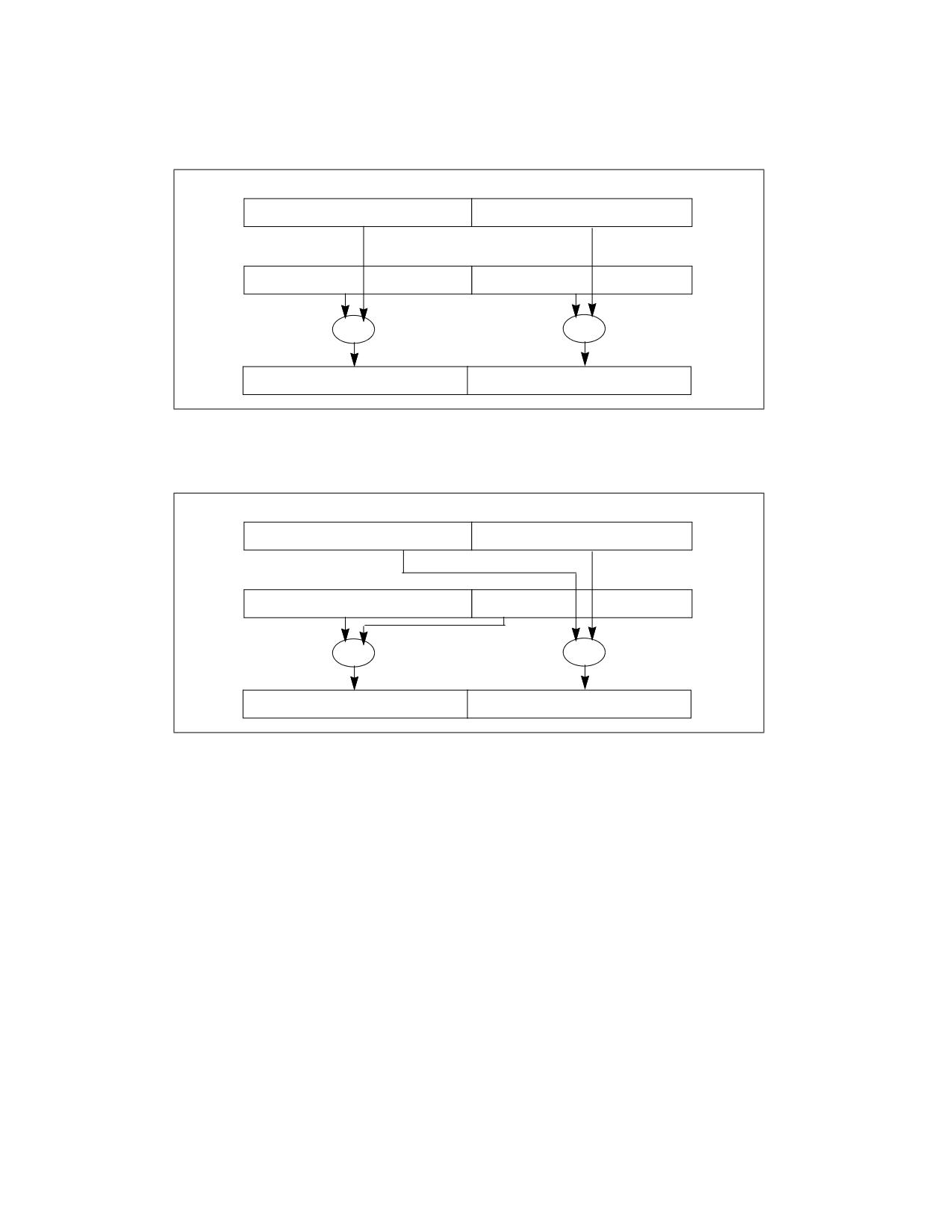
Figure 12-1 illustrates the asymmetric processing of the Intel SSE3 instruction ADDSUBPD. Figure 12-2 illustrates
the horizontal data movement of the Intel SSE3 instruction HADDPD.
X1
X0
Y
1
Y0
ADD
SUB
X1 + Y1
X0 -Y0
Figure 12-1. Asymmetric Processing in ADDSUBPD
X1
X0
Y1
Y0
ADD
ADD
Y0 + Y1
X0 + X1
Figure 12-2. Horizontal Data Movement in HADDPD
12.2
OVERVIEW OF INTEL® SSE3 INSTRUCTIONS
Intel SSE3 extensions include 13 instructions. See:
• Section 12.3, “Intel® SSE3 Instructions,” provides an introduction to individual Intel SSE3 instructions.
• The Intel® 64 and IA-32 Architectures Software Developer’s Manual, Volumes 2A, 2B, 2C, & 2D, provides
detailed information on individual instructions.
• Chapter 16, “System Programming for Instruction Set Extensions and Processor Extended States,” in the Intel®
64 and IA-32 Architectures Software Developer’s Manual, Volume 3A, gives guidelines for integrating Intel
SSE/SSE2/SSE3 extensions into an operating-system environment.
12.3
INTEL® SSE3 INSTRUCTIONS
Intel SSE3 instructions are grouped as follows:
• x87 FPU instruction:
- One instruction that improves x87 FPU floating-point to integer conversion.
12-2
Vol. 1
PROGRAMMING WITH INTEL® SSE3, SSSE3, INTEL® SSE4, AND INTEL® AES-NI
• SIMD integer instruction:
- One instruction that provides a specialized 128-bit unaligned data load.
• SIMD floating-point instructions:
- Three instructions that enhance LOAD/MOVE/DUPLICATE performance.
- Two instructions that provide packed addition/subtraction.
- Four instructions that provide horizontal addition/subtraction.
• Thread synchronization instructions:
- Two instructions that improve synchronization between multi-threaded agents.
The instructions are discussed in more detail in the following paragraphs.
12.3.1 x87 FPU Instruction for Integer Conversion
The FISTTP instruction (x87 FPU Store Integer and Pop with Truncation) behaves like FISTP, but uses truncation
regardless of what rounding mode is specified in the x87 FPU control word. The instruction converts the top of stack
(ST0) to integer with rounding to and pops the stack.
The FISTTP instruction is available in three precisions: short integer (word or 16-bit), integer (double word or 32-
bit), and long integer (64-bit). With FISTTP, applications no longer need to change the FCW when truncation is
required.
12.3.2 SIMD Integer Instruction for Specialized 128-Bit Unaligned Data Load
The LDDQU instruction is a special 128-bit unaligned load designed to avoid cache line splits. If the address of a 16-
byte load is on a 16-byte boundary, LDQQU loads the bytes requested. If the address of the load is not aligned on
a 16-byte boundary, LDDQU loads a 32-byte block starting at the 16-byte aligned address immediately below the
load request. It then extracts the requested 16 bytes.
The instruction provides significant performance improvement on 128-bit unaligned memory accesses at the cost
of some usage model restrictions.
12.3.3 SIMD Floating-Point Instructions That Enhance LOAD/MOVE/DUPLICATE Performance
The MOVSHDUP instruction loads/moves 128-bits, duplicating the second and fourth 32-bit data elements.
• MOVSHDUP OperandA, OperandB
- OperandA (128 bits, four data elements): 3a, 2a, 1a, 0a
- OperandB (128 bits, four data elements): 3b, 2b, 1b, 0b
- Result (stored in OperandA): 3b, 3b, 1b, 1b
The MOVSLDUP instruction loads/moves 128-bits, duplicating the first and third 32-bit data elements.
• MOVSLDUP OperandA, OperandB
- OperandA (128 bits, four data elements): 3a, 2a, 1a, 0a
- OperandB (128 bits, four data elements): 3b, 2b, 1b, 0b
- Result (stored in OperandA): 2b, 2b, 0b, 0b
The MOVDDUP instruction loads/moves 64-bits; duplicating the 64 bits from the source.
• MOVDDUP OperandA, OperandB
- OperandA (128 bits, two data elements): 1a, 0a
- OperandB (64 bits, one data element): 0b
- Result (stored in OperandA): 0b, 0b
Vol. 1
12-3
PROGRAMMING WITH INTEL® SSE3, SSSE3, INTEL® SSE4, AND INTEL® AES-NI
12.3.4 SIMD Floating-Point Instructions Provide Packed Addition/Subtraction
The ADDSUBPS instruction has two 128-bit operands. The instruction performs single precision addition on the
second and fourth pairs of 32-bit data elements within the operands; and single precision subtraction on the first
and third pairs.
• ADDSUBPS OperandA, OperandB
- OperandA (128 bits, four data elements): 3a, 2a, 1a, 0a
- OperandB (128 bits, four data elements): 3b, 2b, 1b, 0b
- Result (stored in OperandA): 3a+3b, 2a-2b, 1a+1b, 0a-0b
The ADDSUBPD instruction has two 128-bit operands. The instruction performs double precision addition on the
second pair of quadwords, and double precision subtraction on the first pair.
• ADDSUBPD OperandA, OperandB
- OperandA (128 bits, two data elements): 1a, 0a
- OperandB (128 bits, two data elements): 1b, 0b
- Result (stored in OperandA): 1a+1b, 0a-0b
12.3.5 SIMD Floating-Point Instructions Provide Horizontal Addition/Subtraction
Most SIMD instructions operate vertically. This means that the result in position i is a function of the elements in
position i of both operands. Horizontal addition/subtraction operates horizontally. This means that contiguous data
elements in the same source operand are used to produce a result.
The HADDPS instruction performs a single precision addition on contiguous data elements. The first data element
of the result is obtained by adding the first and second elements of the first operand; the second element by adding
the third and fourth elements of the first operand; the third by adding the first and second elements of the second
operand; and the fourth by adding the third and fourth elements of the second operand.
• HADDPS OperandA, OperandB
- OperandA (128 bits, four data elements): 3a, 2a, 1a, 0a
- OperandB (128 bits, four data elements): 3b, 2b, 1b, 0b
- Result (Stored in OperandA): 3b+2b, 1b+0b, 3a+2a, 1a+0a
The HSUBPS instruction performs a single precision subtraction on contiguous data elements. The first data
element of the result is obtained by subtracting the second element of the first operand from the first element of
the first operand; the second element by subtracting the fourth element of the first operand from the third element
of the first operand; the third by subtracting the second element of the second operand from the first element of
the second operand; and the fourth by subtracting the fourth element of the second operand from the third
element of the second operand.
• HSUBPS OperandA, OperandB
- OperandA (128 bits, four data elements): 3a, 2a, 1a, 0a
- OperandB (128 bits, four data elements): 3b, 2b, 1b, 0b
- Result (Stored in OperandA): 2b-3b, 0b-1b, 2a-3a, 0a-1a
The HADDPD instruction performs a double precision addition on contiguous data elements. The first data element
of the result is obtained by adding the first and second elements of the first operand; the second element by adding
the first and second elements of the second operand.
• HADDPD OperandA, OperandB
- OperandA (128 bits, two data elements): 1a, 0a
- OperandB (128 bits, two data elements): 1b, 0b
- Result (Stored in OperandA): 1b+0b, 1a+0a
12-4
Vol. 1
PROGRAMMING WITH INTEL® SSE3, SSSE3, INTEL® SSE4, AND INTEL® AES-NI
The HSUBPD instruction performs a double precision subtraction on contiguous data elements. The first data
element of the result is obtained by subtracting the second element of the first operand from the first element of
the first operand; the second element by subtracting the second element of the second operand from the first
element of the second operand.
• HSUBPD OperandA OperandB
- OperandA (128 bits, two data elements): 1a, 0a
- OperandB (128 bits, two data elements): 1b, 0b
- Result (Stored in OperandA): 0b-1b, 0a-1a
12.3.6 Two Thread Synchronization Instructions
The MONITOR instruction sets up an address range that is used to monitor write-back-stores.
MWAIT enables a logical processor to enter into an optimized state while waiting for a write-back-store to the
address range set up by MONITOR. MONITOR and MWAIT require the use of general purpose registers for its input.
The registers used by MONITOR and MWAIT must be initialized properly; register content is not modified by these
instructions.
12.4
WRITING APPLICATIONS WITH INTEL® SSE3
The following sections give guidelines for writing application programs and operating-system code that use Intel
SSE3 instructions.
12.4.1 Guidelines for Using Intel® SSE3
The following guidelines describe how to maximize the benefits of using Intel SSE3:
• Check that the processor supports Intel SSE3.
- Applications may need to ensure that the target operating system supports Intel SSE3. (Operating system
support for the Intel SSE implies sufficient support for Intel SSE2 and SSE3.)
• Ensure your operating system supports MONITOR and MWAIT.
• Employ the optimization and scheduling techniques described in the Intel® 64 and IA-32 Architectures Optimi-
zation Reference Manual (see Section 1.4, “Related Literature”).
12.4.2 Checking for Intel® SSE3 Support
Before an application attempts to use the SIMD subset of Intel SSE3 instructions, the application should follow the
steps illustrated in Section 11.6.2, “Checking for Intel® SSE and SSE2 Support.” Next, use the additional step
provided below:
• Check that the processor supports the SIMD and x87 Intel SSE3 extensions (if CPUID.01H:ECX.SSE3[0] = 1).
An operating system that provides application support for Intel SSE and SSE2 also provides sufficient application
support for Intel SSE3. To use FISTTP, software only needs to check support for Intel SSE3.
In the initial implementation of MONITOR and MWAIT, these two instructions are available to ring 0 and condition-
ally available at ring level greater than 0. Before an application attempts to use the MONITOR and MWAIT instruc-
tions, the application should use the following steps:
1. Check that the processor supports MONITOR and MWAIT. If CPUID.01H:ECX.MONITOR[3] = 1, MONITOR and
MWAIT are available at ring 0.
2. Query the smallest and largest line size that MONITOR uses. Use
CPUID.05H:EAX.SMALLEST[15:0];EBX.LARGEST[15:0]. Values are returned in bytes in EAX and EBX.
3. Ensure the memory address range(s) that will be supplied to MONITOR meets memory type requirements.
Vol. 1
12-5
PROGRAMMING WITH INTEL® SSE3, SSSE3, INTEL® SSE4, AND INTEL® AES-NI
MONITOR and MWAIT are targeted for system software that supports efficient thread synchronization, see Chapter
16 in the Intel® 64 and IA-32 Architectures Software Developer’s Manual, Volume 3A for details.
12.4.3 Enable FTZ and DAZ for SIMD Floating-Point Computation
Enabling the FTZ and DAZ flags in the MXCSR register is likely to accelerate SIMD floating-point computation where
strict compliance to the IEEE standard 754-1985 is not required. The FTZ flag is available to Intel 64 and IA-32
processors that support Intel SSE; DAZ is available to Intel 64 processors and to most IA-32 processors that
support Intel SSE, SSE2, and SSE3.
Software can detect the presence of DAZ, modify the MXCSR register, and save and restore state information by
following the techniques discussed in Section 11.6.3 through Section 11.6.6.
12.4.4 Programming Intel® SSE3 with Intel® SSE and SSE2
SIMD instructions in Intel SSE3 are intended to complement the use of Intel SSE and SSE2 in programming SIMD
applications. Application software that intends to use Intel SSE3 instructions should also check for the availability
of Intel SSE and SSE2 instructions.
The FISTTP instruction in Intel SSE3 is intended to accelerate x87 style programming where performance is limited
by frequent floating-point conversion to integers; this happens when the x87 FPU control word is modified
frequently. Use of the FISTTP instruction can eliminate the need to access the x87 FPU control word.
12.5
OVERVIEW OF SSSE3 INSTRUCTIONS
SSSE3 provides 32 instructions to accelerate a variety of multimedia and signal processing applications employing
SIMD integer data. See:
• Section 12.6, “SSSE3 Instructions,” provides an introduction to individual SSSE3 instructions.
• The Intel® 64 and IA-32 Architectures Software Developer’s Manual, Volumes 2A, 2B, 2C, & 2D, provides
detailed information on individual instructions.
• Chapter 16, “System Programming for Instruction Set Extensions and Processor Extended States,” in the Intel®
64 and IA-32 Architectures Software Developer’s Manual, Volume 3A, gives guidelines for integrating SSSE3
and Intel SSE, SSE2, and SSE3 into an operating-system environment.
12.6
SSSE3 INSTRUCTIONS
SSSE3 instructions include:
• Twelve instructions that perform horizontal addition or subtraction operations.
• Six instructions that evaluate the absolute values.
• Two instructions that perform multiply and add operations and speed up the evaluation of dot products.
• Two instructions that accelerate packed-integer multiply operations and produce integer values with scaling.
• Two instructions that perform a byte-wise, in-place shuffle according to the second shuffle control operand.
• Six instructions that negate packed integers in the destination operand if the signs of the corresponding
element in the source operand is less than zero.
• Two instructions that align data from the composite of two operands.
The operands of these instructions are packed integers of byte, word, or double word sizes. The operands are
stored as 64 or 128 bit data in MMX registers, XMM registers, or memory.
The instructions are discussed in more detail in the following paragraphs.
12-6
Vol. 1
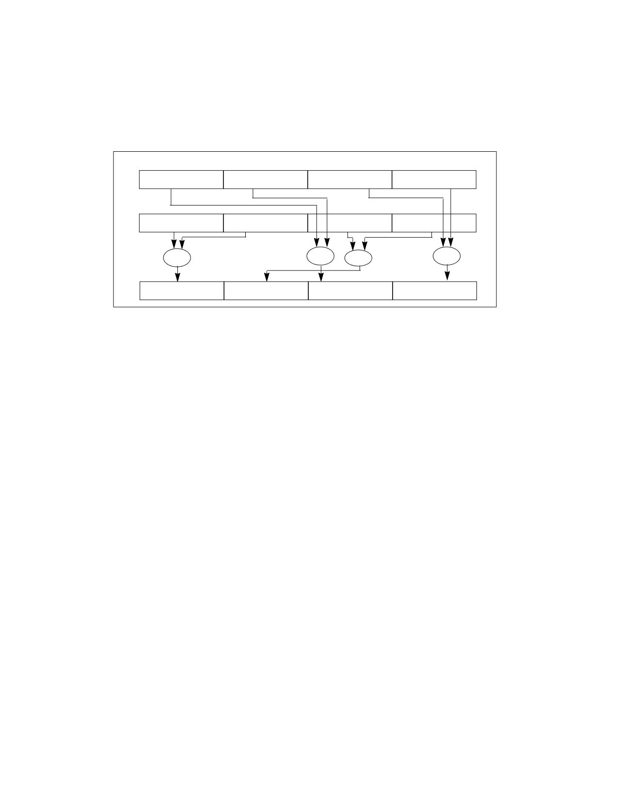
PROGRAMMING WITH INTEL® SSE3, SSSE3, INTEL® SSE4, AND INTEL® AES-NI
12.6.1 Horizontal Addition/Subtraction
In analogy to the packed, floating-point horizontal add and subtract instructions in Intel SSE3, SSSE3 offers similar
capabilities on packed integer data. Data elements of signed words, doublewords are supported. Saturated version
for horizontal add and subtract on signed words are also supported. The horizontal data movement of PHADD is
shown in Figure 12-3.
X3
X2
X1
X0
Y3
Y2
Y1
Y0
ADD
ADD
ADD
ADD
Y2 + Y3
Y0 + Y1
X2 + X3
X0 + X1
Figure 12-3. Horizontal Data Movement in PHADDD
There are six horizontal add instructions (represented by three mnemonics); three operate on 128-bit operands
and three operate on 64-bit operands. The width of each data element is either 16 bits or 32 bits. The mnemonics
are listed below.
• PHADDW adds two adjacent, signed 16-bit integers horizontally from the source and destination operands and
packs the signed 16-bit results to the destination operand.
• PHADDSW adds two adjacent, signed 16-bit integers horizontally from the source and destination operands
and packs the signed, saturated 16-bit results to the destination operand.
• PHADDD adds two adjacent, signed 32-bit integers horizontally from the source and destination operands and
packs the signed 32-bit results to the destination operand.
There are six horizontal subtract instructions (represented by three mnemonics); three operate on 128-bit oper-
ands and three operate on 64-bit operands. The width of each data element is either 16 bits or 32 bits. These are
listed below.
• PHSUBW performs horizontal subtraction on each adjacent pair of 16-bit signed integers by subtracting the
most significant word from the least significant word of each pair in the source and destination operands. The
signed 16-bit results are packed and written to the destination operand.
• PHSUBSW performs horizontal subtraction on each adjacent pair of 16-bit signed integers by subtracting the
most significant word from the least significant word of each pair in the source and destination operands. The
signed, saturated 16-bit results are packed and written to the destination operand.
• PHSUBD performs horizontal subtraction on each adjacent pair of 32-bit signed integers by subtracting the
most significant doubleword from the least significant double word of each pair in the source and destination
operands. The signed 32-bit results are packed and written to the destination operand.
12.6.2 Packed Absolute Values
There are six packed-absolute-value instructions (represented by three mnemonics). Three operate on 128-bit
operands and three operate on 64-bit operands. The widths of data elements are 8 bits, 16 bits or 32 bits. The
absolute value of each data element of the source operand is stored as an UNSIGNED result in the destination
operand.
• PABSB computes the absolute value of each signed byte data element.
Vol. 1
12-7
PROGRAMMING WITH INTEL® SSE3, SSSE3, INTEL® SSE4, AND INTEL® AES-NI
• PABSW computes the absolute value of each signed 16-bit data element.
• PABSD computes the absolute value of each signed 32-bit data element.
12.6.3 Multiply and Add Packed Signed and Unsigned Bytes
There are two multiply-and-add-packed-signed-unsigned-byte instructions (represented by one mnemonic). One
operates on 128-bit operands and the other operates on 64-bit operands. Multiplications are performed on each
vertical pair of data elements. The data elements in the source operand are signed byte values, the input data
elements of the destination operand are unsigned byte values.
• PMADDUBSW multiplies each unsigned byte value with the corresponding signed byte value to produce an
intermediate, 16-bit signed integer. Each adjacent pair of 16-bit signed values are added horizontally. The
signed, saturated 16-bit results are packed to the destination operand.
12.6.4 Packed Multiply High with Round and Scale
There are two packed-multiply-high-with-round-and-scale instructions (represented by one mnemonic). One oper-
ates on 128-bit operands and the other operates on 64-bit operands.
• PMULHRSW multiplies vertically each signed 16-bit integer from the destination operand with the corre-
sponding signed 16-bit integer of the source operand, producing intermediate, signed 32-bit integers. Each
intermediate 32-bit integer is truncated to the 18 most significant bits. Rounding is always performed by adding
1 to the least significant bit of the 18-bit intermediate result. The final result is obtained by selecting the 16 bits
immediately to the right of the most significant bit of each 18-bit intermediate result and packed to the
destination operand.
12.6.5 Packed Shuffle Bytes
There are two packed-shuffle-bytes instructions (represented by one mnemonic). One operates on 128-bit oper-
ands and the other operates on 64-bit operands. The shuffle operations are performed bytewise on the destination
operand using the source operand as a control mask.
• PSHUFB permutes each byte in place, according to a shuffle control mask. The least significant three or four bits
of each shuffle control byte of the control mask form the shuffle index. The shuffle mask is unaffected. If the
most significant bit (bit 7) of a shuffle control byte is set, the constant zero is written in the result byte.
12.6.6 Packed Sign
There are six packed-sign instructions (represented by three mnemonics). Three operate on 128-bit operands and
three operate on 64-bit operands. The widths of each data element for these instructions are 8 bit, 16 bit or 32 bit
signed integers.
• PSIGNB/W/D negates each signed integer element of the destination operand if the sign of the corresponding
data element in the source operand is less than zero.
12.6.7 Packed Align Right
There are two packed-align-right instructions (represented by one mnemonic). One operates on 128-bit operands
and the other operates on 64-bit operands. These instructions concatenate the destination and source operand into
a composite, and extract the result from the composite according to an immediate constant.
• PALIGNR’s source operand is appended after the destination operand forming an intermediate value of twice
the width of an operand. The result is extracted from the intermediate value into the destination operand by
selecting the 128-bit or 64-bit value that are right-aligned to the byte offset specified by the immediate value.
12-8
Vol. 1
PROGRAMMING WITH INTEL® SSE3, SSSE3, INTEL® SSE4, AND INTEL® AES-NI
12.7
WRITING APPLICATIONS WITH SSSE3 EXTENSIONS
The following sections give guidelines for writing application programs and operating-system code that use SSSE3
instructions.
12.7.1 Guidelines for Using SSSE3
The following guidelines describe how to maximize the benefits of using SSSE3:
• Check that the processor supports SSSE3.
• Ensure that your operating system supports SSSE3 and Intel SSE, SSE2, and SSE3. (Operating system support
for Intel SSE implies sufficient support for SSSE3 and Intel SSE2 and SSE3.)
• Employ the optimization and scheduling techniques described in the Intel® 64 and IA-32 Architectures Optimi-
zation Reference Manual (see Section 1.4, “Related Literature”).
12.7.2 Checking for SSSE3 Support
Before an application attempts to use SSSE3, the application should follow the steps illustrated in Section 11.6.2,
“Checking for Intel® SSE and SSE2 Support.” Next, use the additional step provided below:
• Check that the processor supports SSSE3 (if CPUID.01H:ECX.SSSE3[9] = 1).
12.8
INTEL® SSE3, SSSE3, AND INTEL® SSE4 EXCEPTIONS
Intel SSE3, SSSE3, and Intel SSE4 instructions can generate the same type of memory-access and non-numeric
exceptions as other Intel 64 or IA-32 instructions. Existing exception handlers generally handle these exceptions
without code modification.
FISTTP can generate floating-point exceptions. Some Intel SSE3 instructions can also generate SIMD floating-point
exceptions.
Intel SSE3 additions and changes are noted in the following sections. See also: Section 11.5, “Intel® SSE, SSE2,
and SSE3 Exceptions”.
12.8.1 Device Not Available (DNA) Exceptions
Intel SSE3, SSSE3, and Intel SSE4 will cause a DNA Exception (#NM) if the processor attempts to execute an Intel
SSE3 instruction while CR0.TS[bit 3] = 1. If CPUID.01H:ECX.SSE3[0] = 0, execution of an Intel SSE3 instruction
will cause an invalid opcode fault regardless of the state of CR0.TS[bit 3].
Similarly, an attempt to execute an SSSE3 instruction on a processor that reports CPUID.01H:ECX.SSSE3[9] = 0
will cause an invalid opcode fault regardless of the state of CR0.TS[bit 3]. An attempt to execute an Intel SSE4.1
instruction on a processor that reports CPUID.01H:ECX.SSE4_1[19] = 0 will cause an invalid opcode fault regard-
less of the state of CR0.TS[bit 3].
An attempt to execute PCMPGTQ or any one of the four string processing instructions in Intel SSE4.2 on a
processor that reports CPUID.01H:ECX.SSE4_2[20] = 0 will cause an invalid opcode fault regardless of the state of
CR0.TS[bit 3]. CRC32 and POPCNT do not cause #NM.
12.8.2 Numeric Error Flag and IGNNE#
Most Intel SSE3 instructions ignore CR0.NE[bit 5] (treats it as if it were always set) and the IGNNE# pin. With one
exception, all use the exception 19 (#XM) software exception for error reporting. The exception is FISTTP; it
behaves like other x87-FP instructions.
SSSE3 instructions ignore CR0.NE[bit 5] (treats it as if it were always set) and the IGNNE# pin.
Vol. 1
12-9

PROGRAMMING WITH INTEL® SSE3, SSSE3, INTEL® SSE4, AND INTEL® AES-NI
SSSE3 instructions do not cause floating-point errors. Floating-point numeric errors for Intel SSE4.1 are described
in Section 12.8.4. Intel SSE4.2 instructions do not cause floating-point errors.
12.8.3 Emulation
CR0.EM is used by some software to emulate x87 floating-point instructions. CR0.EM[bit 2] cannot be used for
emulation of SSSE3 and Intel SSE, SSE2, SSE3, and SSE4. If an Intel SSE3, SSSE3, or Intel SSE4 instruction
execute with CR0.EM[bit 2] set, an invalid opcode exception (INT 6) is generated instead of a device not available
exception (INT 7).
12.8.4 IEEE 754 Compliance of Intel® SSE4.1 Floating-Point Instructions
The six Intel SSE4.1 instructions that perform floating-point arithmetic are:
• DPPS
• DPPD
• ROUNDPS
• ROUNDPD
• ROUNDSS
• ROUNDSD
Dot Product operations are not specified in IEEE-754. When neither FTZ nor DAZ are enabled, the dot product
instructions resemble sequences of IEEE-754 multiplies and adds (with rounding at each stage), except that the
treatment of input NaN’s is implementation specific (there will be at least one NaN in the output). The input select
fields (bits imm8[4:7]) force input elements to +0.0f prior to the first multiply and will suppress input exceptions
that would otherwise have been be generated.
As a convenience to the exception handler, any exceptions signaled from DPPS or DPPD leave the destination
unmodified.
Round operations signal invalid and precision only.
Table 12-1. SIMD Numeric Exceptions Signaled by SSE4.1
DPPS
DPPD
ROUNDPS
ROUNDPD
ROUNDSS
ROUNDSD
Overflow
X
X
Underflow
X
X
Invalid
X
X
X (1)
X (1)
Inexact Precision
X
X
X (2)
X (2)
Denormal
X
X
NOTE:
1. Invalid is signaled only if Src = SNaN.
2. Precision is ignored (regardless of the MXCSR precision mask) if if imm8[3] = ‘1’.
The other Intel SSE4.1 instructions with floating-point arguments (BLENDPS, BLENDPD, BLENDVPS, BLENDVPD,
INSERTPS, EXTRACTPS) do not signal any SIMD numeric exceptions.
12.9
INTEL® SSE4 OVERVIEW
Intel SSE4 comprises two sets of extensions: Intel SSE4.1 and SSE4.2. Intel SSE4.1 is targeted to improve the
performance of media, imaging, and 3D workloads. Intel SSE4.1 adds instructions that improve compiler vectoriza-
12-10
Vol. 1

PROGRAMMING WITH INTEL® SSE3, SSSE3, INTEL® SSE4, AND INTEL® AES-NI
tion and significantly increase support for packed dword computation. The technology also provides a hint that can
improve memory throughput when reading from uncacheable WC memory type.
The 47 Intel SSE4.1 instructions include:
• Two instructions perform packed dword multiplies.
• Two instructions perform floating-point dot products with input/output selects.
• One instruction performs a load with a streaming hint.
• Six instructions simplify packed blending.
• Eight instructions expand support for packed integer MIN/MAX.
• Four instructions support floating-point round with selectable rounding mode and precision exception override.
• Seven instructions improve data insertion and extractions from XMM registers
• Twelve instructions improve packed integer format conversions (sign and zero extensions).
• One instruction improves SAD (sum absolute difference) generation for small block sizes.
• One instruction aids horizontal searching operations.
• One instruction improves masked comparisons.
• One instruction adds qword packed equality comparisons.
• One instruction adds dword packing with unsigned saturation.
The Intel SSE4.2 instructions operating on XMM registers improve performance in the following areas:
• String and text processing that can take advantage of single-instruction multiple-data programming
techniques.
• A SIMD integer instruction that enhances the capability of the 128-bit integer SIMD capability in Intel SSE4.1.
12.10 INTEL® SSE4.1 INSTRUCTION SET
12.10.1 Dword Multiply Instructions
Intel SSE4.1 adds two dword multiply instructions that aid vectorization. They allow four simultaneous 32 bit by 32
bit multiplies. PMULLD returns a low 32-bits of the result and PMULDQ returns a 64-bit signed result. These repre-
sent the most common integer multiply operation. See Table 12-2.
Table 12-2. Enhanced 32-Bit SIMD Multiply Supported by Intel® SSE4.1
32-Bit Integer Operation
Unsigned x Unsigned
Signed x Signed
Low 32-bit
(not available)
PMULLD
High 32-bit
(not available)
(not available)
64-bit
PMULUDQ*
PMULDQ
NOTE:
* Available prior to Intel SSE4.1.
12.10.2 Floating-Point Dot Product Instructions
Intel SSE4.1 adds two instructions for double precision (for up to 2 elements; DPPD) and single precision dot prod-
ucts (for up to 4 elements; DPPS).
These dot-product instructions include source select and destination broadcast which generally improves the flex-
ibility. For example, a single DPPS instruction can be used for a 2, 3, or 4 element dot product.
Vol. 1
12-11
PROGRAMMING WITH INTEL® SSE3, SSSE3, INTEL® SSE4, AND INTEL® AES-NI
12.10.3 Streaming Load Hint Instruction
Historically, CPU read accesses of WC memory type regions have significantly lower throughput than accesses to
cacheable memory.
The streaming load instruction in SSE4.1, MOVNTDQA, provides a non-temporal hint that can cause adjacent 16-
byte items within an aligned 64-byte region of WC memory type (a streaming line) to be fetched and held in a small
set of temporary buffers (“streaming load buffers”). Subsequent streaming loads to other aligned 16-byte items in
the same streaming line may be satisfied from the streaming load buffer and can improve throughput.
Programmers are advised to use the following practices to improve the efficiency of MOVNTDQA streaming loads
from WC memory:
• Streaming loads must be 16-byte aligned.
• Temporally group streaming loads of the same streaming cache line for effective use of the small number of
streaming load buffers. If loads to the same streaming line are excessively spaced apart, it may cause the
streaming line to be re-fetched from memory.
• Temporally group streaming loads from at most a few streaming lines together. The number of streaming load
buffers is small; grouping a modest number of streams will avoid running out of streaming load buffers and the
resultant re-fetching of streaming lines from memory.
• Avoid writing to a streaming line until all 16-byte-aligned reads from the streaming line have occurred. Reading
a 16-byte item from a streaming line that has been written, may cause the streaming line to be re-fetched.
• Avoid reading a given 16-byte item within a streaming line more than once; repeated loads of a particular 16-
byte item are likely to cause the streaming line to be re-fetched.
• The streaming load buffers, reflecting the WC memory type characteristics, are not required to be snooped by
operations from other agents. Software should not rely upon such coherency actions to provide any data
coherency with respect to other logical processors or bus agents. Rather, software must ensure the consistency
of WC memory accesses between producers and consumers.
• Streaming loads may be weakly ordered and may appear to software to execute out of order with respect to
other memory operations. Software must explicitly use MFENCE if it needs to preserve order among streaming
loads or between streaming loads and other memory operations.
• Streaming loads must not be used to reference memory addresses that are mapped to I/O devices having side
effects or when reads to these devices are destructive. This is because MOVNTDQA is speculative in nature.
Example 12-1 provides a sketch of the basic assembly sequences that illustrate the principles of using MOVNTDQA
in a situation with a producer-consumer accessing a WC memory region.
12-12
Vol. 1

PROGRAMMING WITH INTEL® SSE3, SSSE3, INTEL® SSE4, AND INTEL® AES-NI
Example 12-1. Sketch of MOVNTDQA Usage of a Consumer and a PCI Producer
// P0: producer is a PCI device writing into the WC space
# the PCI device updates status through a UC flag, "u_dev_status" .
# the protocol for "u_dev_status" : 0: produce; 1: consume; 2: all done
mov eax, $0
mov [u_dev_status], eax
producerStart:
mov eax, [u_dev_status]
# poll status flag to see if consumer is requestion data
cmp eax, $0
#
jne done
# I no longer need to produce
commence PCI writes to WC region..
mov eax, $1 # producer ready to notify the consumer via status flag
mov [u_dev_status], eax
# now wait for consumer to signal its status
spinloop:
cmp [u_dev_status], $1
# did I get a signal from the consumer ?
jne producerStart
# yes I did
jmp spinloop
# check again
done:
// producer is finished at this point
// P1: consumer check PCI status flag to consume WC data
mov eax, $0 # request to the producer
mov [u_dev_status], eax
consumerStart:
mov; eax, [u_dev_status] # reads the value of the PCI status
cmp eax, $1
# has producer written
jne consumerStart
# tight loop; make it more efficient with pause, etc.
mfence
# producer finished device writes to WC, ensure WC region is coherent
ntread:
movntdqa xmm0, [addr]
movntdqa xmm1, [addr + 16]
movntdqa xmm2, [addr + 32]
movntdqa xmm3, [addr + 48]
… # do any more NT reads as needed
mfence # ensure PCI device reads the correct value of [u_dev_status]
# now decide whether we are done or we need the producer to produce more data
# if we are done write a 2 into the variable, otherwise write a 0 into the variable
mov eax, $0/$2
# end or continue producing
mov [u_dev_status], eax
# if I want to consume again I will jump back to consumerStart after storing a 0 into eax
# otherwise I am done
Vol. 1
12-13
PROGRAMMING WITH INTEL® SSE3, SSSE3, INTEL® SSE4, AND INTEL® AES-NI
12.10.4 Packed Blending Instructions
Intel SSE4.1 adds 6 instructions used for blending (BLENDPS, BLENDPD, BLENDVPS, BLENDVPD, PBLENDVB,
PBLENDW).
Blending conditionally copies a data element in a source operand to the same element in the destination. Intel
SSE4.1 instructions improve blending operations for most field sizes. A single new Intel SSE4.1 instruction can
generally replace a sequence of 2 to 4 operations using previous architectures.
The variable blend instructions (BLENDVPS, BLENDVPD, PBLENDW) introduce the use of control bits stored in an
implicit XMM register (XMM0). The most significant bit in each field (the sign bit, for 2’s complement integer or
floating-point) is used as a selector. See Table 12-3.
Table 12-3. Blend Field Size and Control Modes Supported by Intel® SSE4.1
Packed
Packed
Packed
Packed
Packed
Instructions
Double FP
Single FP
QWord
DWord
Word
Packed Byte
Blend Control
BLENDPS
X
Imm8
BLENDPD
X
Imm8
BLENDVPS
X
X(1)
XMM0
BLENDVPD
X
X(1)
XMM0
(2)
(2)
(2)
PBLENDVB
X
XMM0
PBLENDW
X
X
X
Imm8
NOTE:
1. Use of floating-point SIMD instructions on integer data types may incur performance penalties.
2. Byte variable blend can be used for larger sized fields by reformatting (or shuffling) the blend control.
12.10.5 Packed Integer MIN/MAX Instructions
Intel SSE4.1 adds 8 packed integer MIN and MAX instructions: PMINUW, PMINUD, PMINSB, PMINSD; PMAXUW,
PMAXUD, PMAXSB, and PMAXSD.
Four 32-bit integer packed MIN and MAX instructions operate on unsigned and signed dwords. Two instructions
operate on signed bytes. Two instructions operate on unsigned words. See Table 12-4.
Table 12-4. Enhanced SIMD Integer MIN/MAX Instructions Supported by Intel® SSE4.1
Integer Width
Byte
Word
DWord
Integer
PMINUB*
PMINUW
PMINUD
Format
Unsigned
PMAXUB*
PMAXUW
PMAXUD
PMINSB
PMINSW*
PMINSD
Signed
PMAXSB
PMAXSW*
PMAXSD
NOTE:
* Available prior to Intel SSE4.1.
12.10.6 Floating-Point Round Instructions with Selectable Rounding Mode
High level languages and libraries often expose rounding operations having a variety of numeric rounding and
exception behaviors. Using Intel SSE, SSE2, and SSE3 instructions to mitigate the rounding-mode-related problem
is sometimes not straight forward.
Intel SSE4.1 introduces four rounding instructions (ROUNDPS, ROUNDPD, ROUNDSS, and ROUNDSD) that cover
scalar and packed single- and double precision floating-point operands. The rounding mode can be selected using
an immediate from one of the IEEE-754 modes (Nearest, -Inf, +Inf, and Truncate) without changing the current
12-14
Vol. 1

PROGRAMMING WITH INTEL® SSE3, SSSE3, INTEL® SSE4, AND INTEL® AES-NI
rounding mode; or the instruction can be forced to use the current rounding mode. Another bit in the immediate is
used to suppress inexact precision exceptions.
Rounding instructions in Intel SSE4.1 generally permit single-instruction solutions to C99 functions ceil(), floor(),
trunc(), rint(), nearbyint(). These instructions simplify the implementations of half-way-away-from-zero rounding
modes as used by C99 round() and F90’s nint().
12.10.7 Insertion and Extractions from XMM Registers
Intel SSE4.1 adds 7 instructions (corresponding to 9 assembly instruction mnemonics) that simplify data insertion
and extraction between general-purpose register (GPR) and XMM registers: EXTRACTPS, INSERTPS, PINSRB,
PINSRD, PINSRQ, PEXTRB, PEXTRW, PEXTRD, and PEXTRQ. When accessing memory, no alignment is required for
any of these instructions (unless alignment checking is enabled).
EXTRACTPS extracts a single precision floating-point value from any dword offset in an XMM register and stores the
result to memory or a general-purpose register. INSERTPS inserts a single floating-point value from either a 32-bit
memory location or from specified element in an XMM register to a selected element in the destination XMM
register. In addition, INSERTPS allows the insertion of +0.0f into any destination elements using a mask.
PINSRB, PINSRD, and PINSRQ insert byte, dword, or qword integer values from a register or memory into an XMM
register. Insertion of integer word values were already supported by Intel SSE2 (PINSRW).
PEXTRB, PEXTRW, PEXTRD, and PEXTRQ extract byte, word, dword, and qword from an XMM register and insert the
values into a general-purpose register or memory.
12.10.8 Packed Integer Format Conversions
A common type of operation on packed integers is the conversion by zero- or sign-extension of packed integers
into wider data types. Intel SSE4.1 adds 12 instructions that convert from a smaller packed integer type to a larger
integer type: PMOVSXBW, PMOVZXBW, PMOVSXBD, PMOVZXBD, PMOVSXWD, PMOVZXWD, PMOVSXBQ,
PMOVZXBQ, PMOVSXWQ, PMOVZXWQ, PMOVSXDQ, and PMOVZXDQ.
The source operand is from either an XMM register or memory; the destination is an XMM register. See Table 12-5.
When accessing memory, no alignment is required for any of the instructions unless alignment checking is enabled.
In which case, all conversions must be aligned to the width of the memory reference. The number of elements
converted (and width of memory reference) is illustrated in Table 12-6. The alignment requirement is shown in
parenthesis.
Table 12-5. New SIMD Integer Conversions Supported by Intel® SSE4.1
Source Type
Byte
Word
Dword
Signed Word
PMOVSXBW
Unsigned Word
PMOVZXBW
Signed Dword
PMOVSXBD
PMOVSXWD
Unsigned Dword
PMOVZXBD
PMOVZXWD
Signed Qword
PMOVSXBQ
PMOVSXWQ
PMOVSXDQ
Unsigned Qword
PMOVZXBQ
PMOVZXWQ
PMOVZXDQ
Vol. 1
12-15
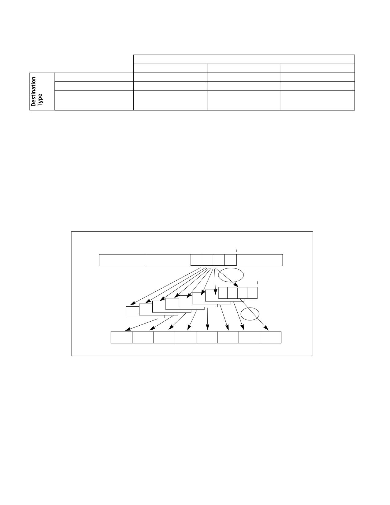
PROGRAMMING WITH INTEL® SSE3, SSSE3, INTEL® SSE4, AND INTEL® AES-NI
Table 12-6. New SIMD Integer Conversions Supported by Intel® SSE4.1
Source Type
Byte
Word
Dword
Word
8 (64 bits)
Dword
4 (32 bits)
4 (64 bits)
Qword
2 (16 bits)
2 (32 bits)
2 (64 bits)
12.10.9 Improved Sums of Absolute Differences (SAD) for 4-Byte Blocks
Intel SSE4.1 adds an instruction (MPSADBW) that performs eight 4-byte wide SAD operations per instruction to
produce eight results. Compared to PSADBW, MPSADBW operates on smaller chunks (4-byte instead of 8-byte
chunks); this makes the instruction better suited to video coding standards such as VC.1 and H.264. MPSADBW
performs four times the number of absolute difference operations than that of PSADBW (per instruction). This can
improve performance for dense motion searches.
MPSADBW uses a 4-byte wide field from a source operand; the offset of the 4-byte field within the 128-bit source
operand is specified by two immediate control bits. MPSADBW produces eight 16-bit SAD results. Each 16-bit SAD
result is formed from overlapping pairs of 4 bytes in the destination with the 4-byte field from the source operand.
MPSADBW uses eleven consecutive bytes in the destination operand, its offset is specified by a control bit in the
immediate byte (i.e., the offset can be from byte 0 or from byte 4). Figure 12-4 illustrates the operation of
MPSADBW. MPSADBW can simplify coding of dense motion estimation by providing source and destination offset
control, higher throughput of SAD operations, and the smaller chunk size.
Imm[1:0]*32
127
96
64
0
Source
Abs. Diff.
Imm[2]*32
Destination
Sum
127
16
0
Figure 12-4. MPSADBW Operation
12.10.10 Horizontal Search
Intel SSE4.1 adds a search instruction (PHMINPOSUW) that finds the value and location of the minimum unsigned
word from one of 8 horizontally packed unsigned words. The resulting value and location (offset within the source)
are packed into the low dword of the destination XMM register.
Rapid search is often a significant component of motion estimation. MPSADBW and PHMINPOSUW can be used
together to improve video encode.
12-16
Vol. 1

PROGRAMMING WITH INTEL® SSE3, SSSE3, INTEL® SSE4, AND INTEL® AES-NI
12.10.11 Packed Test
The packed test instruction PTEST is similar to a 128-bit equivalent to the legacy instruction TEST. With PTEST, the
source argument is typically used like a bit mask.
PTEST performs a logical AND between the destination with this mask and sets the ZF flag if the result is zero. The
CF flag (zero for TEST) is set if the inverted mask AND’d with the destination is all zero. Because the destination is
not modified, PTEST simplifies branching operations (such as branching on signs of packed floating-point numbers,
or branching on zero fields).
12.10.12 Packed Qword Equality Comparisons
Intel SSE4.1 adds a 128-bit packed qword equality test. The new instruction (PCMPEQQ) is identical to PCMPEQD,
but has qword granularity.
12.10.13 Dword Packing With Unsigned Saturation
Intel SSE4.1 adds a new instruction PACKUSDW to complete the set of small integer pack instructions in the family
of SIMD instruction extensions. PACKUSDW packs dword to word with unsigned saturation. See Table 12-7 for the
complete set of packing instructions for small integers.
Table 12-7. Enhanced SIMD Pack Support by Intel® SSE4.1
Pack Type
DWord -> Word
Word -> Byte
Unsigned
PACKUSDW (new!)
PACKUSWB
Signed
PACKSSDW
PACKSSWB
12.11 INTEL® SSE4.2 INSTRUCTION SET
Five of the seven Intel SSE4.2 instructions can use an XMM register as a source or destination. These include four
text/string processing instructions and one packed quadword compare SIMD instruction. Programming these five
Intel SSE4.2 instructions is similar to programming 128-bit Integer SIMD in Intel SSE2 or SSSE3. Intel SSE4.2
does not provide any 64-bit integer SIMD instructions.
12.11.1 String and Text Processing Instructions
String and text processing instructions in Intel SSE4.2 allocates four opcodes to provide a rich set of string and text
processing capabilities that traditionally required many more opcodes. These four instructions use XMM registers
to process string or text elements of up to 128-bits (16 bytes or 8 words). Each instruction uses an immediate byte
to support a rich set of programmable controls. A string-processing Intel SSE4.2 instruction returns the result of
processing each pair of string elements using either an index or a mask.
The capabilities of the string/text processing instructions include:
• Handling string/text fragments consisting of bytes or words, either signed or unsigned.
• Support for partial string or fragments less than 16 bytes in length, using either explicit length or implicit null-
termination.
• Four types of string compare operations on word/byte elements.
• Up to 256 compare operations performed in a single instruction on all string/text element pairs.
• Built-in aggregation of intermediate results from comparisons.
Vol. 1
12-17
PROGRAMMING WITH INTEL® SSE3, SSSE3, INTEL® SSE4, AND INTEL® AES-NI
• Programmable control of processing on intermediate results.
• Programmable control of output formats in terms of an index or mask.
• Bi-directional support for the index format.
• Support for two mask formats: bit or natural element width.
• Not requiring 16-byte alignment for memory operand.
The four Intel SSE4.2 instructions that process text/string fragments are:
• PCMPESTRI - Packed compare explicit-length strings, return index in ECX/RCX.
• PCMPESTRM - Packed compare explicit-length strings, return mask in XMM0.
• PCMPISTRI - Packed compare implicit-length strings, return index in ECX/RCX.
• PCMPISTRM - Packed compare implicit-length strings, return mask in XMM0.
All four of these instructions require the use of an immediate byte to control operation. The two source operands
can be XMM registers or a combination of XMM register and memory address. The immediate byte provides
programmable control with the following attributes:
• Input data format.
• Compare operation mode.
• Intermediate result processing.
• Output selection.
Depending on the output format associated with the instruction, the text/string processing instructions implicitly
uses either a general-purpose register (ECX/RCX) or an XMM register (XMM0) to return the final result.
Two of the four text-string processing instructions specify string length explicitly. They use two general-purpose
registers (EDX, EAX) to specify the number of valid data elements (either word or byte) in the source operands. The
other two instructions specify valid string elements using null termination. A data element is considered valid only
if it has a lower index than the least significant null data element.
12.11.1.1 Memory Operand Alignment
The text and string processing instructions in Intel SSE4.2 do not perform alignment checking on memory oper-
ands. This is different from most other 128-bit SIMD instructions accessing the XMM registers. The absence of an
alignment check for these four instructions does not imply any modification to the existing definitions of other
instructions.
12.11.2 Packed Comparison SIMD Integer Instruction
Intel SSE4.2 also provides a 128-bit integer SIMD instruction PCMPGTQ that performs logical compare of greater-
than on packed integer quadwords.
12.12 WRITING APPLICATIONS WITH INTEL® SSE4 EXTENSIONS
12.12.1 Guidelines for Using Intel® SSE4 Extensions
The following guidelines describe how to maximize the benefits of using Intel SSE4 extensions:
• Check that the processor supports Intel SSE4 extensions.
• Ensure that the operating system supports SSSE3 and Intel SSE, SSE2, and SSE3. (Operating system support
for Intel SSE implies sufficient support for SSSE3 and Intel SSE2, SSE3, and SSE4.)
• Employ the optimization and scheduling techniques described in the Intel® 64 and IA-32 Architectures Optimi-
zation Reference Manual (see Section 1.4, “Related Literature”).
12-18
Vol. 1

PROGRAMMING WITH INTEL® SSE3, SSSE3, INTEL® SSE4, AND INTEL® AES-NI
12.12.2 Checking for Intel® SSE4.1 Support
Before an application attempts to use Intel SSE4.1 instructions, the application should follow the steps illustrated
in Section 11.6.2, “Checking for Intel® SSE and SSE2 Support.” Next, use the additional step provided below:
Check that the processor supports Intel SSE4.1 (if CPUID.01H:ECX.SSE4_1[19] = 1), Intel SSE3 (if
CPUID.01H:ECX.SSE3[0] = 1), and SSSE3 (if CPUID.01H:ECX.SSSE3[9] = 1).
12.12.3 Checking for Intel® SSE4.2 Support
Before an application attempts to use the following Intel SSE4.2 instructions: PCMPESTRI/PCMPESTRM/PCMP-
ISTRI/PCMPISTRM, PCMPGTQ; the application should follow the steps illustrated in Section 11.6.2, “Checking for
Intel® SSE and SSE2 Support.” Next, use the additional steps provided below:
• Check that the processor supports Intel SSE4.2 (if CPUID.01H:ECX.SSE4_2[20] = 1), Intel SSE4.1 (if
CPUID.01H:ECX.SSE4_1[19] = 1), and SSSE3 (if CPUID.01H:ECX.SSSE3[9] = 1).
• Before an application attempts to use the CRC32 instruction, it must check that the processor supports Intel
SSE4.2 (if CPUID.01H:ECX.SSE4_2[20] = 1).
• Before an application attempts to use the POPCNT instruction, it must check that the processor supports Intel
SSE4.2 (if CPUID.01H:ECX.SSE4_2[20] = 1) and POPCNT (if CPUID.01H:ECX.POPCNT[23] = 1).
12.13 INTEL® AES-NI OVERVIEW
Intel AES-NI provides six instructions to accelerate symmetric block encryption/decryption of 128-bit data blocks
using the Advanced Encryption Standard (AES) specified by the NIST publication FIPS 197. Specifically, two
instructions (AESENC and AESENCLAST) target the AES encryption rounds; and two instructions (AESDEC and
AESDECLAST) target AES decryption rounds using the Equivalent Inverse Cipher. One instruction (AESIMC) targets
the Inverse MixColumn transformation primitive, and one instruction (AESKEYGEN) targets generation of round
keys from the cipher key for the AES encryption/decryption rounds.
AES supports encryption/decryption using cipher key lengths of 128, 192, and 256 bits by processing the data
block in 10, 12, and 14 rounds of predefined transformations. Figure 12-5 depicts the cryptographic processing of
a block of 128-bit plain text into cipher text.
RK(0)
RK(1)
RK(n-1)
XOR
Rounds 2.. n-2
Round 1
Last
Round
Plain text
AES State
AES State
AES State
Cipher text
n-1
AES-128: n = 10
AES-192: n = 12
AES-256: n = 14
Figure 12-5. AES State Flow
The predefined AES transformation primitives are described in the next few sections, they are also referenced in
the operation flow of instruction reference page of these instructions.
12.13.1 Little-Endian Architecture and Big-Endian Specification (FIPS 197)
FIPS 197 document defines the Advanced Encryption Standard (AES) and includes a set of test vectors for testing
all of the steps in the algorithm, and can be used for testing and debugging.
Vol. 1
12-19
PROGRAMMING WITH INTEL® SSE3, SSSE3, INTEL® SSE4, AND INTEL® AES-NI
The following observation is important for using the AES instructions offered in Intel 64 Architecture: FIPS 197 text
convention is to write hex strings with the low-memory byte on the left and the high-memory byte on the right.
Intel’s convention is the reverse. It is similar to the difference between Big Endian and Little Endian notations.
In other words, a 128 bits vector in the FIPS document, when read from left to right, is encoded as [7:0, 15:8,
23:16, 31:24, …127:120]. Note that inside the byte, the encoding is [7:0], so the first bit from the left is the most
significant bit. In practice, the test vectors are written in hexadecimal notation, where pairs of hexadecimal digits
define the different bytes. To translate the FIPS 197 notation to an Intel 64 architecture compatible (“Little
Endian”) format, each test vector needs to be byte-reflected to [127:120,… 31:24, 23:16, 15:8, 7:0].
Example A:
FIPS Test vector: 000102030405060708090a0b0c0d0e0fH
Intel AES Hardware: 0f0e0d0c0b0a09080706050403020100H
It should be pointed out that the only thing at issue is a textual convention, and programmers do not need to
perform byte-reversal in their code, when using the AES instructions.
12.13.1.1 AES Data Structure in Intel® 64 Architecture
The AES instructions that are defined in this document operate on one or on two 128 bits source operands: State
and Round Key. From the architectural point of view, the state is input in an xmm register and the Round key is
input either in an xmm register or a 128-bit memory location.
In AES algorithm, the state (128 bits) can be viewed as four 32-bit doublewords (“Words” in AES terminology): X3,
X2, X1, and X0.
The state may also be viewed as a set of 16 bytes. The 16 bytes can also be viewed as a 4x4 matrix of bytes where
S(i, j) with i, j = 0, 1, 2, 3 compose the 32-bit “words” as follows:
X0 = S (3, 0) S (2, 0) S (1, 0) S (0, 0)
X1 = S (3, 1) S (2, 1) S (1, 1) S (0, 1)
X2 = S (3, 2) S (2, 2) S (1, 2) S (0, 2)
X3 = S (3, 3) S (2, 3) S (1, 3) S (0, 3)
The following tables, Table 12-8 through Table 12-11, illustrate various representations of a 128-bit state.
Table 12-8. Byte and 32-Bit Word Representation of a 128-Bit State
Byte #
15
14
13
12
11
10
9
8
7
6
5
4
3
2
1
0
Bit Position
127-
119-
111-
103-
95-
87-
79-
71-
63-
55-
47-
39-
31-
23-
15-
7-
120
112
103
96
88
80
72
64
56
48
40
32
24
16
8
0
127 - 96
95 - 64
64 - 32
31 - 0
State Word
X3
X2
X1
X0
State Byte
P
O
N
M
L
K
J
I
H
G
F
E
D
C
B
A
Table 12-9. Matrix Representation of a 128-Bit State
A
E
I
M
S(0, 0)
S(0, 1)
S(0, 2)
S(0, 3)
B
F
J
N
S(1, 0)
S(1, 1)
S(1, 2)
S(1, 3)
C
G
K
O
S(2, 0)
S(2, 1)
S(2, 2)
S(2, 3)
D
H
L
P
S(3, 0)
S(3, 1)
S(3, 2)
S(3, 3)
Example:
FIPS vector: d4 bf 5d 30 e0 b4 52 ae b8 41 11 f1 1e 27 98 e5
12-20
Vol. 1

PROGRAMMING WITH INTEL® SSE3, SSSE3, INTEL® SSE4, AND INTEL® AES-NI
This vector has the “least significant” byte d4 and the significant byte e5 (written in Big Endian format in the FIPS
document). When it is translated to IA notations, the encoding is:
Table 12-10. Little Endian Representation of a 128-Bit State
Byte #
15
14
13
12
11
10
9
8
7
6
5
4
3
2
1
0
State Byte
P
O
N
M
L
K
J
I
H
G
F
E
D
C
B
A
State Value
e5
98
27
1e
f1
11
41
b8
ae
52
b4
e0
30
5d
bf
d4
Table 12-11. Little Endian Representation of a 4x4 Byte Matrix
A
E
I
M
d4
e0
b8
1e
B
F
J
N
bf
b4
41
27
C
G
K
O
5d
52
11
98
D
H
L
P
30
ae
f1
e5
12.13.2 AES Transformations and Functions
The following functions and transformations are used in the algorithmic descriptions of AES instruction extensions
AESDEC, AESDECLAST, AESENC, AESENCLAST, AESIMC, and AESKEYGENASSIST.
Note that these transformations are expressed here in a Little Endian format (and not as in the FIPS 197 docu-
ment).
• MixColumns(): A byte-oriented 4x4 matrix transformation on the matrix representation of a 128-bit AES state.
A FIPS-197 defined 4x4 matrix is multiplied to each 4x1 column vector of the AES state. The columns are
considered polynomials with coefficients in the Finite Field that is used in the definition of FIPS 197, the
operations (“multiplication” and “addition”) are in that Finite Field, and the polynomials are reduced modulo
x4+1.
The MixColumns() transformation defines the relationship between each byte of the result state, represented
as S’(i, j) of a 4x4 matrix (see Section 12.13.1), as a function of input state bytes, S(i, j), as follows
S’(0, j) := FF_MUL( 02H, S(0, j) ) XOR FF_MUL(03H, S(1, j) ) XOR S(2, j) XOR S(3, j)
S’(1, j) := S(0, j) XOR FF_MUL( 02H, S(1, j) ) XOR FF_MUL(03H, S(2, j) ) XOR S(3, j)
S’(2, j) := S(0, j) XOR S(1, j) XOR FF_MUL( 02H, S(2, j) ) XOR FF_MUL(03H, S(3, j) )
S’(3, j) := FF_MUL(03H, S(0, j) ) XOR S(1, j) XOR S(2, j) XOR FF_MUL( 02H, S(3, j) )
where j = 0, 1, 2, 3. FF_MUL(Byte1, Byte2) denotes the result of multiplying two elements (represented by
Byte1 and byte2) in the Finite Field representation that defines AES. The result of produced bye
FF_MUL(Byte1, Byte2) is an element in the Finite Field (represented as a byte). A Finite Field is a field with a
finite number of elements, and when this number can be represented as a power of 2 (2n), its elements can
be represented as the set of 2n binary strings of length n. AES uses a finite field with n=8 (having 256
elements). With this representation, “addition” of two elements in that field is a bit-wise XOR of their binary-
string representation, producing another element in the field. Multiplication of two elements in that field is
defined using an irreducible polynomial (for AES, this polynomial is m(x) = x8 + x4 + x3 + x + 1). In this
Finite Field representation, the bit value of bit position k of a byte represents the coefficient of a polynomial of
order k, e.g., 1010_1101B (ADH) is represented by the polynomial (x7 + x5 + x3 + x2 + 1). The byte value
result of multiplication of two elements is obtained by a carry-less multiplication of the two corresponding
polynomials, followed by reduction modulo the polynomial, where the remainder is calculated using
operations defined in the field. For example, FF_MUL(57H, 83H) = C1H, because the carry-less polynomial
multiplication of the polynomials represented by 57H and 83H produces (x13 + x11 + x9 + x8 + x6 + x5 + x4
+ x3 + 1), and the remainder modulo m(x) is (x7 + x6 + 1).
• RotWord(): performs a byte-wise cyclic permutation (rotate right in little-endian byte order) on a 32-bit AES
word.
Vol. 1
12-21

PROGRAMMING WITH INTEL® SSE3, SSSE3, INTEL® SSE4, AND INTEL® AES-NI
The output word X’[j] of RotWord(X[j]) where X[j] represent the four bytes of column j, S(i, j), in descending
order X[j] = ( S(3, j), S(2, j), S(1, j), S(0, j) ); X’[j] = ( S’(3, j), S’(2, j), S’(1, j), S’(0, j) ) := ( S(0, j), S(3,
j), S(2, j), S(1, j) )
•
ShiftRows(): A byte-oriented matrix transformation that processes the matrix representation of a 16-byte AES
state by cyclically shifting the last three rows of the state by different offset to the left, see Table 12-12.
Table 12-12. The ShiftRows Transformation
Matrix Representation of Input State
Output of ShiftRows
A
E
I
M
A
E
I
M
B
F
J
N
F
J
N
B
C
G
K
O
K
O
C
G
D
H
L
P
P
D
H
L
•
SubBytes(): A byte-oriented transformation that processes the 128-bit AES state by applying a non-linear
substitution table (S-BOX) on each byte of the state.
The SubBytes() function defines the relationship between each byte of the result state S’(i, j) as a function of
input state byte S(i, j), by
S’(i, j) := S-Box (S(i, j)[7:4], S(i, j)[3:0])
where S-BOX (S[7:4], S[3:0]) represents a look-up operation on a 16x16 table to return a byte value, see
Table 12-13.
Table 12-13. Look-up Table Associated with S-Box Transformation
S[3:0]
0
1
2
3
4
5
6
7
8
9
a
b
c
d
e
f
0
63
7c
77
7b
f2
6b
6f
c5
30
01
67
2b
fe
d7
ab
76
1
ca
82
c9
7d
fa
59
47
f0
ad
d4
a2
af
9c
a4
72
c0
2
b7
fd
93
26
36
3f
f7
cc
34
a5
e5
f1
71
d8
31
15
3
04
c7
23
c3
18
96
05
9a
07
12
80
e2
eb
27
b2
75
4
09
83
2c
1a
1b
6e
5a
a0
52
3b
d6
b3
29
e3
2f
84
5
53
d1
00
ed
20
fc
b1
5b
6a
cb
be
39
4a
4c
58
cf
6
d0
ef
aa
fb
43
4d
33
85
45
f9
02
7f
50
3c
9f
a8
7
51
a3
40
8f
92
9d
38
f5
bc
b6
da
21
10
ff
f3
d2
S[7:4]
8
cd
0c
13
ec
5f
97
44
17
c4
a7
7e
3d
64
5d
19
73
9
60
81
4f
dc
22
2a
90
88
46
ee
b8
14
de
5e
0b
db
a
e0
32
3a
0a
49
06
24
5c
c2
d3
ac
62
91
95
e4
79
b
e7
c8
37
6d
8d
d5
4e
a9
6c
56
f4
ea
65
7a
ae
08
c
ba
78
25
2e
1c
a6
b4
c6
e8
dd
74
1f
4b
bd
8b
8a
d
70
3e
b5
66
48
03
f6
0e
61
35
57
b9
86
c1
1d
9e
e
e1
f8
98
11
69
d9
8e
94
9b
1e
87
e9
ce
55
28
df
f
8c
a1
89
0d
bf
e6
42
68
41
99
2d
0f
b0
54
bb
16
• SubWord(): produces an output AES word (four bytes) from the four bytes of an input word using a non-linear
substitution table (S-BOX).
12-22
Vol. 1

PROGRAMMING WITH INTEL® SSE3, SSSE3, INTEL® SSE4, AND INTEL® AES-NI
X’[j] = ( S’(3, j), S’(2, j), S’(1, j), S’(0, j) ) := ( S-Box (S(3, j)), S-Box( S(2, j) ), S-Box( S(1, j) ), S-Box(
S(0, j) ))
•
InvMixColumns(): The inverse transformation of MixColumns().
The InvMixColumns() transformation defines the relationship between each byte of the result state S’(i, j) as
a function of input state bytes, S(i, j), by
S’(0, j) := FF_MUL( 0eH, S(0, j) ) XOR FF_MUL(0bH, S(1, j) ) XOR FF_MUL(0dH, S(2, j) ) XOR FF_MUL( 09H,
S(3, j) )
S’(1, j) := FF_MUL(09H, S(0, j) ) XOR FF_MUL( 0eH, S(1, j) ) XOR FF_MUL(0bH, S(2, j) ) XOR FF_MUL( 0dH,
S(3, j) )
S’(2, j) := FF_MUL(0dH, S(0, j) ) XOR FF_MUL( 09H, S(1, j) ) XOR FF_MUL( 0eH, S(2, j) ) XOR FF_MUL(0bH,
S(3, j) )
S’(3, j) := FF_MUL(0bH, S(0, j) ) XOR FF_MUL(0dH, S(1, j) ) XOR FF_MUL( 09H, S(2, j) ) XOR FF_MUL( 0eH,
S(3, j) ), where j = 0, 1, 2, 3.
•
InvShiftRows(): The inverse transformation of InvShiftRows(). The InvShiftRows() transforms the matrix
representation of a 16-byte AES state by cyclically shifting the last three rows of the state by different offset to
the right, see Table 12-14.
Table 12-14. The InvShiftRows Transformation
Matrix Representation of Input State
Output of ShiftRows
A
E
I
M
A
E
I
M
B
F
J
N
N
B
F
J
C
G
K
O
K
O
C
G
D
H
L
P
H
L
P
D
•
InvSubBytes(): The inverse transformation of SubBytes().
The InvSubBytes() transformation defines the relationship between each byte of the result state S’(i, j) as a
function of input state byte S(i, j), by
S’(i, j) := InvS-Box (S(i, j)[7:4], S(i, j)[3:0])
where InvS-BOX (S[7:4], S[3:0]) represents a look-up operation on a 16x16 table to return a byte value, see
Table 12-15.
Vol. 1
12-23

PROGRAMMING WITH INTEL® SSE3, SSSE3, INTEL® SSE4, AND INTEL® AES-NI
Table 12-15. Look-up Table Associated with InvS-Box Transformation
S[3:0]
0
1
2
3
4
5
6
7
8
9
a
b
c
d
e
f
0
52
09
6a
d5
30
36
a5
38
bf
40
a3
9e
81
f3
d7
fb
1
7c
e3
39
82
9b
2f
ff
87
34
8e
43
44
c4
de
e9
cb
2
54
7b
94
32
a6
c2
23
3d
ee
4c
95
0b
42
fa
c3
4e
3
08
2e
a1
66
28
d9
24
b2
76
5b
a2
49
6d
8b
d1
25
4
72
f8
f6
64
86
68
98
16
d4
a4
5c
cc
5d
65
b6
92
5
6c
70
48
50
fd
ed
b9
da
5e
15
46
57
a7
8d
9d
84
6
90
d8
ab
00
8c
bc
d3
0a
f7
e4
58
05
b8
b3
45
06
7
d0
2c
1e
8f
ca
3f
0f
02
c1
af
bd
03
01
13
8a
6b
S[7:4]
8
3a
91
11
41
4f
67
dc
ea
97
f2
cf
ce
f0
b4
e6
73
9
96
ac
74
22
e7
ad
35
85
e2
f9
37
e8
1c
75
df
6e
a
47
f1
1a
71
1d
29
c5
89
6f
b7
62
0e
aa
18
be
1b
b
fc
56
3e
4b
c6
d2
79
20
9a
db
c0
fe
78
cd
5a
f4
c
1f
dd
a8
33
88
07
c7
31
b1
12
10
59
27
80
ec
5f
d
60
51
7f
a9
19
b5
4a
0d
2d
e5
7a
9f
93
c9
9c
ef
e
a0
e0
3b
4d
ae
2a
f5
b0
c8
eb
bb
3c
83
53
99
61
f
17
2b
04
7e
ba
77
d6
26
e1
69
14
63
55
21
0c
7d
12.13.3 PCLMULQDQ
The PCLMULQDQ instruction performs carry-less multiplication of two 64-bit data into a 128-bit result. Carry-less
multiplication of two 128-bit data into a 256-bit result can use PCLMULQDQ as building blocks.
Carry-less multiplication is a component of many cryptographic systems. It is an important piece of implementing
Galois Counter Mode (GCM) operation of block ciphers. GCM operation can be used in conjunction with AES algo-
rithms to add authentication capability. GCM usage models also include IPsec, storage standard, and security
protocols over fiber channel. Additionally, PCLMULQDQ can be used in calculations of hash functions and CRC using
arbitrary polynomials.
12.13.4 Checking for Intel® AES-NI Support
Before an application attempts to use AESNI instructions or PCLMULQDQ, the application should follow the steps
illustrated in Section 11.6.2, “Checking for Intel® SSE and SSE2 Support.” Next, use the additional step provided
below:
Check that the processor supports Intel AES-NI (if CPUID.01H:ECX.AESNI[25] = 1); check that the processor
supports PCLMULQDQ (if CPUID.01H:ECX.PCLMULQDQ[1] = 1).
12-24
Vol. 1
CHAPTER 13
MANAGING STATE USING THE XSAVE FEATURE SET
The XSAVE feature set extends the functionality of the FXSAVE and FXRSTOR instructions (see Section 10.5,
“FXSAVE and FXRSTOR Instructions”) by supporting the saving and restoring of processor state in addition to the
x87 execution environment (x87 state) and the registers used by the streaming SIMD extensions (SSE state).
The XSAVE feature set comprises eight instructions. XGETBV and XSETBV allow software to read and write the
extended control register XCR0, which controls the operation of the XSAVE feature set. XSAVE, XSAVEOPT,
XSAVEC, and XSAVES are four instructions that save processor state to memory; XRSTOR and XRSTORS are corre-
sponding instructions that load processor state from memory. XGETBV, XSAVE, XSAVEOPT, XSAVEC, and XRSTOR
can be executed at any privilege level; XSETBV, XSAVES, and XRSTORS can be executed only if CPL = 0. In addition
to XCR0, the XSAVES and XRSTORS instructions are controlled also by the IA32_XSS MSR (index DA0H).
The XSAVE feature set organizes the state that manages into state components. Operation of the instructions is
based on state-component bitmaps that have the same format as XCR0 and as the IA32_XSS MSR: each bit
corresponds to a state component. Section 13.1 discusses these state components and bitmaps in more detail.
Section 13.2 describes how the processor enumerates support for the XSAVE feature set and for XSAVE-enabled
features (those features that require the use of the XSAVE feature set for their enabling). Section 13.3 explains
how software can enable the XSAVE feature set and XSAVE-enabled features.
The XSAVE feature set allows saving and loading processor state from a region of memory called an XSAVE area.
Section 13.4 presents details of the XSAVE area and its organization. Each XSAVE-managed state component is
associated with a section of the XSAVE area. Section 13.5 describes in detail each of the XSAVE-managed state
components.
Section 13.7 through Section 13.12 describe the operation of XSAVE, XRSTOR, XSAVEOPT, XSAVEC, XSAVES, and
XRSTORS, respectively.
Section 13.13 provides some details about memory accesses performed by instructions in the XSAVE feature set,
and Section 13.14 describes a facility called extended feature disable (XFD).
13.1
XSAVE-SUPPORTED FEATURES AND STATE-COMPONENT BITMAPS
The XSAVE feature set supports the saving and restoring of state components, each of which is a discrete set of
processor registers (or parts of registers). In general, each such state component corresponds to a particular CPU
feature. Such a feature is XSAVE-supported. Some XSAVE-supported features use registers in multiple XSAVE-
managed state components.
The XSAVE feature set organizes the state components of the XSAVE-supported features using state-component
bitmaps. A state-component bitmap comprises 64 bits; each bit in such a bitmap corresponds to a single state
component. The following bits are defined in state-component bitmaps (details on individual state components are
provided in subsections of Section 13.5):
• Bit 0 corresponds to the state component used for the x87 FPU execution environment (x87 state).
• Bit 1 corresponds to the state component used for registers used by the streaming SIMD extensions (SSE
state).
• Bit 2 corresponds to the state component used for the additional register state used by the Intel® Advanced
Vector Extensions (AVX state).
• Bits 4:3 correspond to the two state components used for the additional register state used by Intel® Memory
Protection Extensions (MPX state):
- State component 3 is used for the 4 128-bit bounds registers BND0-BND3 (BNDREGS state).
- State component 4 is used for the 64-bit user-mode MPX configuration register BNDCFGU and the 64-bit
MPX status register BNDSTATUS (BNDCSR state).
• Bits 7:5 correspond to the three state components used for the additional register state used by Intel®
Advanced Vector Extensions 512 (AVX-512 state):
Vol. 1
13-1
MANAGING STATE USING THE XSAVE FEATURE SET
- State component 5 is used for the 8 64-bit opmask registers k0-k7 (opmask state).
- State component 6 is used for the upper 256 bits of the registers ZMM0-ZMM15. These 16 256-bit values
are denoted ZMM0_H-ZMM15_H (ZMM_Hi256 state).
- State component 7 is used for the 16 512-bit registers ZMM16-ZMM31 (Hi16_ZMM state).
• Bit 8 corresponds to the state component used for the Intel Processor Trace MSRs (PT state).
• Bit 9 corresponds to the state component used for the protection-key feature’s register PKRU (PKRU state).
• Bit 10 corresponds to the state component used for the IA32_PASID MSR used by the ENQCMD instruction for
a process address space identifiers (PASID state).
• Bits 12:11 correspond to the two state components used for the additional register state used by Control-Flow
Enforcement Technology (CET state):
- State component 11 is used for the 2 MSRs controlling user-mode functionality for CET (CET_U state).
- State component 12 is used for the 3 MSRs containing shadow-stack pointers for privilege levels 0-2
(CET_S state).
• Bit 13 corresponds to the state component used for an MSR used to control hardware duty cycling (HDC
state).
• Bit 14 corresponds to the state component used for user interrupts (UINTR state).
• Bit 15 corresponds to the state component used for last-branch record configuration (LBR state).
• Bit 16 corresponds to the state component used for an MSR used to control hardware P-states (HWP state).
• Bits 18:17 correspond to the two state components used for the additional register state used by Intel®
Advanced Matrix Extensions (AMX state):
- State component 17 is used for the 64-byte TILECFG register (TILECFG state).
- State component 18 is used for the 8192 bytes of tile data (TILEDATA state).
Bits in the range 62:19 are not currently defined in state-component bitmaps and are reserved for future expan-
sion. As individual state components are defined using those bits, additional sub-sections will be updated within
Section 13.5 over time. Bit 63 is used for special functionality in some bitmaps and does not correspond to any
state component.
The state component corresponding to bit i of state-component bitmaps is called state component i. Thus, x87
state is state component 0; SSE state is state component 1; AVX state is state component 2; MPX state comprises
state components 3-4; AVX-512 state comprises state components 5-7; PT state is state component 8; PKRU state
is state component 9; PASID state is state component 10; CET state comprises state components 11-12; HDC
state is state component 13; UINTR state is state component 14; LBR state is state component 15; HWP state is
state component 16; AMX state comprises state components 17-18.
The XSAVE feature set uses state-component bitmaps in multiple ways. Most of the instructions use an implicit
operand (in EDX:EAX), called the instruction mask, which is the state-component bitmap that specifies the state
components on which the instruction operates.
Some state components are user state components, and they can be managed by the entire XSAVE feature set.
Other state components are supervisor state components, and they can be managed only by XSAVES and
XRSTORS. The state components corresponding to bit 9, to bits 18:17, and to bits in the range 7:0 are user state
components; those corresponding to bit 8, to bits in the range 13:10, and to bits 16:14 are supervisor state
components.
Extended control register XCR0 contains a state-component bitmap that specifies the user state components that
software has enabled the XSAVE feature set to manage. If the bit corresponding to a state component is clear in
XCR0, instructions in the XSAVE feature set will not operate on that state component, regardless of the value of the
instruction mask.
The IA32_XSS MSR (index DA0H) contains a state-component bitmap that specifies the supervisor state compo-
nents that software has enabled XSAVES and XRSTORS to manage (XSAVE, XSAVEC, XSAVEOPT, and XRSTOR
cannot manage supervisor state components). If the bit corresponding to a state component is clear in the
IA32_XSS MSR, XSAVES and XRSTORS will not operate on that state component, regardless of the value of the
instruction mask.
13-2
Vol. 1
MANAGING STATE USING THE XSAVE FEATURE SET
Some XSAVE-supported features can be used only if XCR0 has been configured so that the features’ state compo-
nents can be managed by the XSAVE feature set. (This applies only to features with user state components.) Such
state components and features are XSAVE-enabled. In general, the processor will not modify (or allow modifica-
tion of) the registers of a state component of an XSAVE-enabled feature if the bit corresponding to that state
component is clear in XCR0. (If software clears such a bit in XCR0, the processor preserves the corresponding state
component.) If an XSAVE-enabled feature has not been fully enabled in XCR0, execution of any instruction defined
for that feature causes an invalid-opcode exception (#UD).
As will be explained in Section 13.3, the XSAVE feature set is enabled only if CR4.OSXSAVE[bit 18] = 1. If
CR4.OSXSAVE = 0, the processor treats XSAVE-enabled state features and their state components as if all bits in
XCR0 were clear; the state components cannot be modified and the features’ instructions cannot be executed.
The state components for x87 state, for SSE state, for PT state, for PKRU state, for PASID state, for CET state, for
HDC state, for UINTR state, for LBR state, and for HWP state are XSAVE-managed but the corresponding features
are not XSAVE-enabled. Processors allow modification of this state, as well as execution of x87 FPU instructions
and SSE instructions and use of Intel Processor Trace, protection keys, the ENQCMD instruction and the
IA32_PASID MSR, CET, hardware duty cycling, user interrupts, LBRs, and hardware P-states, regardless of the
value of CR4.OSXSAVE and XCR0.
13.2
ENUMERATION OF CPU SUPPORT FOR XSAVE INSTRUCTIONS AND XSAVE-
SUPPORTED FEATURES
A processor enumerates support for the XSAVE feature set and for features supported by that feature set using the
CPUID instruction. The following items provide specific details:
• CPUID.01H:ECX.XSAVE[26] enumerates general support for the XSAVE feature set:
- If this bit is 0, the processor does not support any of the following instructions: XGETBV, XRSTOR,
XRSTORS, XSAVE, XSAVEC, XSAVEOPT, XSAVES, and XSETBV; the processor provides no further
enumeration through CPUID.0DH (see below).
- If this bit is 1, the processor supports the following instructions: XGETBV, XRSTOR, XSAVE, and XSETBV.1
Further enumeration is provided through CPUID.0DH.
CR4.OSXSAVE can be set to 1 if and only if CPUID.01H:ECX.XSAVE[26] is enumerated as 1.
• CPUID.0DH enumerates details of CPU support through a set of sub-leaves. Software selects a specific sub-leaf
by the value placed in the ECX register. The following items provide specific details:
- CPUID.0DH.00H.
• EDX:EAX is a bitmap of all the user state components that can be managed using the XSAVE feature
set. A bit can be set in XCR0 if and only if the corresponding bit is set in this bitmap. Every processor
that supports the XSAVE feature set will set EAX[0] (x87 state) and EAX[1] (SSE state).
If EAX[i] = 1 (for 1 < i < 32) or EDX[i-32] = 1 (for 32 ≤ i < 63), sub-leaf i enumerates details for state
component i (see below).
• ECX enumerates the size (in bytes) required by the XSAVE instruction for an XSAVE area containing all
the user state components supported by this processor.
• EBX enumerates the size (in bytes) required by the XSAVE instruction for an XSAVE area containing all
the user state components corresponding to bits currently set in XCR0.
- CPUID.0DH.01H.
• EAX[0] enumerates support for the XSAVEOPT instruction. The instruction is supported if and only if
this bit is 1. If EAX[0] = 0, execution of XSAVEOPT causes an invalid-opcode exception (#UD).
• EAX[1] enumerates support for compaction extensions to the XSAVE feature set. The following are
supported if this bit is 1:
1. If CPUID.01H:ECX.XSAVE[26] = 1, XGETBV and XSETBV may be executed with ECX = 0 (to read and write XCR0). Any support for
execution of these instructions with other values of ECX is enumerated separately.
Vol. 1
13-3
MANAGING STATE USING THE XSAVE FEATURE SET
- The compacted format of the extended region of XSAVE areas (see Section 13.4.3).
- The XSAVEC instruction. If EAX[1] = 0, execution of XSAVEC causes a #UD.
- Execution of the compacted form of XRSTOR (see Section 13.8).
• EAX[2] enumerates support for execution of XGETBV with ECX = 1. This allows software to determine
the state of the init optimization. See Section 13.6.
• EAX[3] enumerates support for XSAVES, XRSTORS, and the IA32_XSS MSR. If EAX[3] = 0, execution
of XSAVES or XRSTORS causes a #UD; an attempt to access the IA32_XSS MSR using RDMSR or
WRMSR causes a general-protection exception (#GP). Every processor that supports a supervisor state
component sets EAX[3]. Every processor that sets EAX[3] (XSAVES, XRSTORS, IA32_XSS) will also set
EAX[1] (the compaction extensions).
• EAX[4] enumerates general support for extended feature disable (XFD). See Section 13.14 for details.
• EAX[31:5] are reserved.
• EBX enumerates the size (in bytes) defined as follows:
- If EAX[3] is enumerated as 1, EBX enumerates the size required by the XSAVES instruction for an
XSAVE area containing all the state components corresponding to bits currently set in XCR0 |
IA32_XSS.
- If EAX[3] is enumerated as 0 and EAX[1] is enumerated as 1, EBX enumerates the size required by
the XSAVEC instruction for an XSAVE area containing all the state components corresponding to bits
currently set in XCR0.
- If EAX[1] and EAX[3] are both enumerated as 0, EBX enumerates zero.
• EDX:ECX is a bitmap of all the supervisor state components that can be managed by XSAVES and
XRSTORS. A bit can be set in the IA32_XSS MSR if and only if the corresponding bit is set in this bitmap.
NOTE
In summary, the XSAVE feature set supports state componenti (0≤ i< 63) if one of the following is
true: (1) i< 32 and CPUID.0DH.00H:EAX[i] = 1; (2) i ≥ 32 and CPUID.0DH.00H:EDX[i-32] = 1;
(3) i< 32 and CPUID.0DH.01H:ECX[i] = 1; or (4) i ≥ 32 and CPUID.0DH.01H:EDX[i-32] = 1. The
XSAVE feature set supports user state component i if (1) or (2) holds; if (3) or (4) holds, state
componenti is a supervisor state component and support is limited to XSAVES and XRSTORS.
- CPUID.0DH.i (i > 1). This sub-leaf enumerates details for state component i. If the XSAVE feature set
supports state component i (see note above), the following items provide specific details:
• EAX enumerates the size (in bytes) required for state component i.
• If state component i is a user state component, EBX enumerates the offset (in bytes, from the base of
the XSAVE area) of the section used for state component i. (This offset applies only when the standard
format for the extended region of the XSAVE area is being used; see Section 13.4.3.)
• If state component i is a supervisor state component, EBX returns 0.
• If state component i is a user state component, ECX[0] return 0; if state component i is a supervisor
state component, ECX[0] returns 1.
• The value returned by ECX[1] indicates the alignment of state component i when the compacted format
of the extended region of an XSAVE area is used (see Section 13.4.3). If ECX[1] returns 0, state
component i is located immediately following the preceding state component; if ECX[1] returns 1, state
component i is located on the next 64-byte boundary following the preceding state component.
• If the processor supports XFD for state component i, ECX[2] returns 1; otherwise, ECX[2] returns 0.
• ECX[31:3] and EDX return 0.
If the XSAVE feature set does not support state component i, sub-leaf i returns 0 in EAX, EBX, ECX, and
EDX.
13-4
Vol. 1
MANAGING STATE USING THE XSAVE FEATURE SET
13.3
ENABLING THE XSAVE FEATURE SET AND XSAVE-ENABLED FEATURES
Software enables the XSAVE feature set by setting CR4.OSXSAVE[bit 18] to 1 (e.g., with the MOV to CR4 instruc-
tion). If this bit is 0, execution of any of XGETBV, XRSTOR, XRSTORS, XSAVE, XSAVEC, XSAVEOPT, XSAVES, and
XSETBV causes an invalid-opcode exception (#UD).
When CR4.OSXSAVE = 1 and CPL = 0, executing the XSETBV instruction with ECX = 0 writes the 64-bit value in
EDX:EAX to XCR0 (EAX is written to XCR0[31:0] and EDX to XCR0[63:32]). (Execution of the XSETBV instruction
causes a general-protection fault - #GP - if CPL > 0.) The following items provide details regarding individual bits
in XCR0:
•
XCR0[0] is associated with x87 state (see Section 13.5.1). XCR0[0] is always 1. It has that value coming out of
RESET. Executing the XSETBV instruction causes a general-protection fault (#GP) if ECX = 0 and EAX[0] is 0.
•
XCR0[1] is associated with SSE state (see Section 13.5.2). Software can use the XSAVE feature set to manage
SSE state only if XCR0[1] = 1. The value of XCR0[1] in no way determines whether software can execute SSE
instructions (these instructions can be executed even if XCR0[1] = 0).
XCR0[1] is 0 coming out of RESET. As noted in Section 13.2, every processor that supports the XSAVE feature
set allows software to set XCR0[1].
•
XCR0[2] is associated with AVX state (see Section 13.5.3). Software can use the XSAVE feature set to manage
AVX state only if XCR0[2] = 1. In addition, software can execute Intel AVX instructions only if CR4.OSXSAVE =
XCR0[2] = 1. Otherwise, any execution of an Intel AVX instruction causes an invalid-opcode exception (#UD).
XCR0[2] is 0 coming out of RESET. As noted in Section 13.2, a processor allows software to set XCR0[2] if and
only if CPUID.0DH.00H:EAX[2] = 1. In addition, executing the XSETBV instruction causes a general-protection
fault (#GP) if ECX = 0 and EAX[2:1] has the value 10b; that is, software cannot enable the XSAVE feature set
for AVX state but not for SSE state.
As noted in Section 13.1, the processor will preserve AVX state unmodified if software clears XCR0[2].
However, clearing XCR0[2] while AVX state is not in its initial configuration may cause SSE instructions to incur
a power and performance penalty. See Section 16.5.3, “Enable the Use Of XSAVE Feature Set And XSAVE State
Components,” of the Intel® 64 and IA-32 Architectures Software Developer’s Manual, Volume 3A, for how
system software can avoid this penalty.
•
XCR0[4:3] are associated with MPX state (see Section 13.5.4). Software can use the XSAVE feature set to
manage MPX state only if XCR0[4:3] = 11b. In addition, MPX instructions operate as defined only if
CR4.OSXSAVE = 1 and XCR0[4:3] = 11b. Otherwise, execution of an MPX instruction causes no operation (as
a NOP instruction); in addition, executions of CALL, RET, JMP, and Jcc do not initialize the bounds registers, and
they ignore any F2H (BND) prefix.1
XCR0[4:3] have value 00b coming out of RESET. As noted in Section 13.2, a processor allows software to set
XCR0[4:3] to 11b if and only if CPUID.0DH.00H:EAX[4:3] = 11b. In addition, executing the XSETBV instruction
causes a general-protection fault (#GP) if ECX = 0, EAX[4:3] is neither 00b nor 11b; that is, software can
enable the XSAVE feature set for MPX state only if it does so for both state components.
As noted in Section 13.1, the processor will preserve MPX state unmodified if software clears XCR0[4:3].
•
XCR0[7:5] are associated with AVX-512 state (see Section 13.5.5). Software can use the XSAVE feature set to
manage AVX-512 state only if XCR0[7:5] = 111b. In addition, software can execute Intel AVX-512 instructions
only if CR4.OSXSAVE = 1 and XCR0[7:5] = 111b. Otherwise, any execution of an Intel AVX-512 instruction
causes an invalid-opcode exception (#UD).
XCR0[7:5] have value 000b coming out of RESET. As noted in Section 13.2, a processor allows software to set
XCR0[7:5] to 111b if and only if CPUID.0DH.00H:EAX[7:5] = 111b. In addition, executing the XSETBV
instruction causes a general-protection fault (#GP) if ECX = 0, EAX[7:5] is not 000b, and any bit is clear in
EAX[2:1] or EAX[7:5]; that is, software can enable the XSAVE feature set for AVX-512 state only if it does so
for all three state components, and only if it also does so for AVX state and SSE state. This implies that the
value of XCR0[7:5] is always either 000b or 111b.
As noted in Section 13.1, the processor will preserve AVX-512 state unmodified if software clears XCR0[7:5].
However, clearing XCR0[7:5] while AVX-512 state is not in its initial configuration may cause SSE and Intel AVX
instructions to incur a power and performance penalty. See Section 16.5.3, “Enable the Use Of XSAVE Feature
1.
Prior to the introduction of MPX, the opcodes defining MPX instructions operated as NOP, and the CALL, RET, JMP, and Jcc instruc-
tions ignored any F2H prefix.
Vol. 1
13-5
MANAGING STATE USING THE XSAVE FEATURE SET
Set And XSAVE State Components,” of the Intel® 64 and IA-32 Architectures Software Developer’s Manual,
Volume 3A, for how system software can avoid this penalty.
• XCR0[9] is associated with PKRU state (see Section 13.5.7). Software can use the XSAVE feature set to
manage PKRU state only if XCR0[9] = 1. The value of XCR0[9] in no way determines whether software can use
protection keys or execute other instructions that access PKRU state (these instructions can be executed even
if XCR0[9] = 0).
XCR0[9] is 0 coming out of RESET. As noted in Section 13.2, a processor allows software to set XCR0[9] if and
only if CPUID.0DH.00H:EAX[9] = 1.
• XCR0[18:17] are associated with AMX state (see Section 13.5.14). Software can use the XSAVE feature set to
manage AMX state only if XCR0[18:17] = 11b. In addition, software can execute Intel AMX instructions only if
CR4.OSXSAVE = 1 and XCR0[18:17] = 11b. Otherwise, any execution of an Intel AMX instruction causes an
invalid-opcode exception (#UD).
XCR0[18:17] have value 00b coming out of RESET. As noted in Section 13.2, a processor allows software to set
XCR0[18:17] to 11b if and only if CPUID.0DH.00H:EAX[18:17] = 11b. In addition, executing the XSETBV
instruction causes a general-protection fault (#GP) if ECX = 0 and EAX[17] ≠ EAX[18] (TILECFG and TILEDATA
must be enabled together). This implies that the value of XCR0[18:17] is always either 00b or 11b.
While Intel AMX instructions can be executed only in 64-bit mode, instructions of the XSAVE feature set can
operate on TILECFG and TILEDATA in any mode. It is recommended that only 64-bit operating systems enable
Intel AMX by setting XCR0[18:17].
• XCR0[63:19], XCR0[16:10], and XCR0[8] are reserved.1 Executing the XSETBV instruction causes a general-
protection fault (#GP) if ECX = 0 and any corresponding bit in EDX:EAX is not 0. These bits in XCR0 are all 0
coming out of RESET.
Software operating with CPL > 0 may need to determine whether the XSAVE feature set and certain XSAVE-
enabled features have been enabled. If CPL > 0, execution of the MOV from CR4 instruction causes a general-
protection fault (#GP). The following alternative mechanisms allow software to discover the enabling of the XSAVE
feature set regardless of CPL:
• The value of CR4.OSXSAVE is returned in CPUID.01H:ECX.OSXSAVE[27]. If software determines that
CPUID.01H:ECX.OSXSAVE = 1, the processor supports the XSAVE feature set and the feature set has been
enabled in CR4.
• Executing the XGETBV instruction with ECX = 0 returns the value of XCR0 in EDX:EAX. XGETBV can be
executed if CR4.OSXSAVE = 1 (if CPUID.01H:ECX.OSXSAVE = 1), regardless of CPL.
Thus, software can use the following algorithm to determine the support and enabling for the XSAVE feature set:
1. Use CPUID to discover the value of CPUID.01H:ECX.OSXSAVE.
- If the bit is 0, either the XSAVE feature set is not supported by the processor or has not been enabled by
software. Either way, the XSAVE feature set is not available, nor are XSAVE-enabled features such as AVX.
- If the bit is 1, the processor supports the XSAVE feature set - including the XGETBV instruction - and it
has been enabled by software. The XSAVE feature set can be used to manage x87 state (because XCR0[0]
is always 1). Software requiring more detailed information can go on to the next step.
2. Execute XGETBV with ECX = 0 to discover the value of XCR0. If XCR0[1] = 1, the XSAVE feature set can be
used to manage SSE state. If XCR0[2] = 1, the XSAVE feature set can be used to manage AVX state and
software can execute Intel AVX instructions. If XCR0[4:3] is 11b, the XSAVE feature set can be used to manage
MPX state and software can execute Intel MPX instructions. If XCR0[7:5] is 111b, the XSAVE feature set can be
used to manage AVX-512 state and software can execute Intel AVX-512 instructions. If XCR0[9] = 1, the
XSAVE feature set can be used to manage PKRU state.
The IA32_XSS MSR (with MSR index DA0H) is zero coming out of RESET. If CR4.OSXSAVE = 1,
CPUID.0DH.01H:EAX[3] = 1, and CPL= 0, executing the WRMSR instruction with ECX = DA0H writes the 64-bit
value in EDX:EAX to the IA32_XSS MSR (EAX is written to IA32_XSS[31:0] and EDX to IA32_XSS[63:32]). The
following items provide details regarding individual bits in the IA32_XSS MSR:
1. Bit 8 and bits 16:10 correspond to supervisor state components. Since bits can be set in XCR0 only for user state components, those
bits of XCR0 must be 0.
13-6
Vol. 1
MANAGING STATE USING THE XSAVE FEATURE SET
• IA32_XSS[8] is associated with PT state (see Section 13.5.6). Software can use XSAVES and XRSTORS to
manage PT state only if IA32_XSS[8] = 1. The value of IA32_XSS[8] does not determine whether software can
use Intel Processor Trace (the feature can be used even if IA32_XSS[8] = 0).
• IA32_XSS[10] is associated with PASID state (see Section 13.5.8). Software can use the XSAVES and
XRSTORS to manage PASID state only if IA32_XSS[10] = 1. The value of IA32_XSS[10] does not determine
whether software can use the ENQCMD instruction, which uses the IA32_PASID MSR. (ENQCMD can be used
even if IA32_XSS[10] is 0.)
• IA32_XSS[12:11] are associated with CET state (see Section 13.5.9), IA32_XSS[11] with CET_U state and
IA32_XSS[12] with CET_S state. Software can use the XSAVES and XRSTORS to manage CET_U state (respec-
tively, CET_S state) only if IA32_XSS[11] = 1 (respectively, IA32_XSS[12] = 1). The value of
IA32_XSS[12:11] does not determine whether software can use CET (the feature can be used even if either of
IA32_XSS[12:11] is 0).
• IA32_XSS[13] is associated with HDC state (see Section 13.5.10). Software can use XSAVES and XRSTORS to
manage HDC state only if IA32_XSS[13] = 1. The value of IA32_XSS[13] does not determine whether software
can use hardware duty cycling (the feature can be used even if IA32_XSS[13] = 0).
• IA32_XSS[14] is associated with UINTR state (see Section 13.5.11). Software can use XSAVES and XRSTORS
to manage UINTR state only if IA32_XSS[14] = 1. The value of IA32_XSS[14] does not determine whether
software can use user interrupts (the feature can be used even if IA32_XSS[14] = 0).
• IA32_XSS[15] is associated with LBR state (see Section 13.5.12). Software can use XSAVES and XRSTORS to
manage LBR state only if IA32_XSS[15] = 1. The value of IA32_XSS[15] does not determine whether software
can use LBRs (the feature can be used even if IA32_XSS[15] = 0).
• IA32_XSS[16] is associated with HWP state (see Section 13.5.13). Software can use XSAVES and XRSTORS to
manage HWP state only if IA32_XSS[16] = 1. The value of IA32_XSS[16] does not determine whether
software can use hardware P-states (the feature can be used even if IA32_XSS[16] = 0).
• IA32_XSS[63:17], IA32_XSS[9] and IA32_XSS[7:0] are reserved.1 Executing the WRMSR instruction causes
a general-protection fault (#GP) if ECX = DA0H and any corresponding bit in EDX:EAX is not 0. These bits in
XCR0 are all 0 coming out of RESET.
The IA32_XSS MSR is 0 coming out of RESET.
There is no mechanism by which software operating with CPL > 0 can discover the value of the IA32_XSS MSR.
13.4
XSAVE AREA
The XSAVE feature set includes instructions that save and restore the XSAVE-managed state components to and
from memory: XSAVE, XSAVEOPT, XSAVEC, and XSAVES (for saving); and XRSTOR and XRSTORS (for restoring).
The processor organizes the state components in a region of memory called an XSAVE area. Each of the save and
restore instructions takes a memory operand that specifies the 64-byte aligned base address of the XSAVE area on
which it operates.
Every XSAVE area has the following format:
• The legacy region. The legacy region of an XSAVE area comprises the 512 bytes starting at the area’s base
address. It is used to manage the state components for x87 state and SSE state. The legacy region is described
in more detail in Section 13.4.1.
• The XSAVE header. The XSAVE header of an XSAVE area comprises the 64 bytes starting at an offset of 512
bytes from the area’s base address. The XSAVE header is described in more detail in Section 13.4.2.
• The extended region. The extended region of an XSAVE area starts at an offset of 576 bytes from the area’s
base address. It is used to manage the state components other than those for x87 state and SSE state. The
extended region is described in more detail in Section 13.4.3. The size of the extended region is determined by
which state components the processor supports and which bits have been set in XCR0 and IA32_XSS (see
Section 13.3).
1. Bit 9 and bits 7:0 correspond to user state components. Since bits can be set in the IA32_XSS MSR only for supervisor state compo-
nents, those bits of the MSR must be 0.
Vol. 1
13-7

MANAGING STATE USING THE XSAVE FEATURE SET
13.4.1 Legacy Region of an XSAVE Area
The legacy region of an XSAVE area comprises the 512 bytes starting at the area’s base address. It has the same
format as the FXSAVE area (see Section 10.5.1). The XSAVE feature set uses the legacy area for x87 state (state
component 0) and SSE state (state component 1). Table 13-1 illustrates the format of the first 416 bytes of the
legacy region of an XSAVE area.
Table 13-1. Format of the Legacy Region of an XSAVE Area
15
14
13
12
11
10
9
8
7
6
5
4
3
2
1
0
FIP[63:48] or
FCS or
FIP[31:0]
FOP
Rsvd.
FTW
FSW
FCW
0
reserved
FIP[47:32]
FDP[63:48]
FDS or
MXCSR_MASK
MXCSR
FDP[31:0]
16
or reserved
FDP[47:32]
Reserved
ST0/MM0
32
Reserved
ST1/MM1
48
Reserved
ST2/MM2
64
Reserved
ST3/MM3
80
Reserved
ST4/MM4
96
Reserved
ST5/MM5
112
Reserved
ST6/MM6
128
Reserved
ST7/MM7
144
XMM0
160
XMM1
176
XMM2
192
XMM3
208
XMM4
224
XMM5
240
XMM6
256
XMM7
272
XMM8
288
XMM9
304
XMM10
320
XMM11
336
XMM12
352
XMM13
368
XMM14
384
XMM15
400
The x87 state component comprises bytes 23:0 and bytes 159:32. The SSE state component comprises
bytes 31:24 and bytes 415:160. The XSAVE feature set does not use bytes 511:416; bytes 463:416 are reserved.
Section 13.7 through Section 13.9 provide details of how instructions in the XSAVE feature set use the legacy
region of an XSAVE area.
13-8
Vol. 1
MANAGING STATE USING THE XSAVE FEATURE SET
13.4.2 XSAVE Header
The XSAVE header of an XSAVE area comprises the 64 bytes starting at offset 512 from the area’s base address:
• Bytes 7:0 of the XSAVE header is a state-component bitmap (see Section 13.1) called XSTATE_BV. It
identifies the state components in the XSAVE area.
• Bytes 15:8 of the XSAVE header is a state-component bitmap called XCOMP_BV. It is used as follows:
- XCOMP_BV[63] indicates the format of the extended region of the XSAVE area (see Section 13.4.3). If it is
clear, the standard format is used. If it is set, the compacted format is used; XCOMP_BV[62:0] provide
format specifics as specified in Section 13.4.3.
- XCOMP_BV[63] determines which form of the XRSTOR instruction is used. If the bit is set, the compacted
form is used; otherwise, the standard form is used. See Section 13.8.
- All bits in XCOMP_BV should be 0 if the processor does not support the compaction extensions to the XSAVE
feature set.
• Bytes 63:16 of the XSAVE header are reserved.
Section 13.7 through Section 13.9 provide details of how instructions in the XSAVE feature set use the XSAVE
header of an XSAVE area.
13.4.3 Extended Region of an XSAVE Area
The extended region of an XSAVE area starts at byte offset 576 from the area’s base address. The size of the
extended region is determined by which state components the processor supports and which bits have been set in
XCR0 | IA32_XSS (see Section 13.3). The XSAVE feature set uses the extended area for each state component i,
where i ≥ 2.
The extended region of the an XSAVE area may have one of two formats. The standard format is supported by all
processors that support the XSAVE feature set; the compacted format is supported by those processors that
support the compaction extensions to the XSAVE feature set (see Section 13.2). Bit 63 of the XCOMP_BV field in
the XSAVE header (see Section 13.4.2) indicates which format is used.
The following items describe the two possible formats of the extended region:
• Standard format. Each state component i (i≥ 2) is located at the byte offset from the base address of the
XSAVE area enumerated in CPUID.0DH.i:EBX. (CPUID.0DH.i:EAX enumerates the number of bytes required for
state component i.
• Compacted format. Each state component i (i ≥ 2) is located at a byte offset from the base address of the
XSAVE area based on the XCOMP_BV field in the XSAVE header:
- If XCOMP_BV[i] = 0, state component i is not in the XSAVE area.
- If XCOMP_BV[i] = 1, state component i is located at a byte offset locationI from the base address of the
XSAVE area, where locationI is determined by the following items:
• If XCOMP_BV[j] = 0 for every j, 2 ≤ j < i, locationI is 576. (This item applies if i is the first bit set in
bits 62:2 of the XCOMP_BV; it implies that state component i is located at the beginning of the
extended region.)
• Otherwise, let j, 2≤ j< i, be the greatest value such that XCOMP_BV[j] = 1. Then locationI is determined
by the following values: locationJ; sizeJ, as enumerated in CPUID.0DH.j:EAX; and the value of alignI, as
enumerated in CPUID.0DH.i:ECX[1]:
- If alignI = 0, locationI = locationJ + sizeJ. (This item implies that state component i is located
immediately following the preceding state component whose bit is set in XCOMP_BV.)
- If alignI = 1, locationI = ceiling(locationJ + sizeJ, 64). (This item implies that state component i is
located on the next 64-byte boundary following the preceding state component whose bit is set in
XCOMP_BV.)
Vol. 1
13-9
MANAGING STATE USING THE XSAVE FEATURE SET
13.5
XSAVE-MANAGED STATE
The section provides details regarding how the XSAVE feature set interacts with the various XSAVE-managed state
components.
Unless otherwise state, the state pertaining to a particular state component is saved beginning at byte 0 of the
section of the XSAVE are corresponding to that state component.
13.5.1 x87 State
Instructions in the XSAVE feature set can manage the same state of the x87 FPU execution environment (x87
state) that can be managed using the FXSAVE and FXRSTOR instructions. They organize all x87 state as a user
state component in the legacy region of the XSAVE area (see Section 13.4.1). This region is illustrated in
Table 13-1; the x87 state is listed below, along with details of its interactions with the XSAVE feature set:
• Bytes 1:0, 3:2, 7:6. These are used for the x87 FPU Control Word (FCW), the x87 FPU Status Word (FSW), and
the x87 FPU Opcode (FOP), respectively.
• Byte 4 is used for an abridged version of the x87 FPU Tag Word (FTW). The following items describe its usage:
- For each j, 0 ≤ j ≤ 7, XSAVE, XSAVEOPT, XSAVEC, and XSAVES save a 0 into bit j of byte 4 if x87 FPU data
register STj has a empty tag; otherwise, XSAVE, XSAVEOPT, XSAVEC, and XSAVES save a 1 into bit j of byte
4.
- For each j, 0 ≤ j ≤ 7, XRSTOR and XRSTORS establish the tag value for x87 FPU data register STj as follows.
If bit j of byte 4 is 0, the tag for STj in the tag register for that data register is marked empty (11B);
otherwise, the x87 FPU sets the tag for STj based on the value being loaded into that register (see below).
• Bytes 15:8 are used as follows:
- If the instruction has no REX prefix, or if REX.W = 0:
• Bytes 11:8 are used for bits 31:0 of the x87 FPU Instruction Pointer Offset (FIP).
• If CPUID.07H.00H:EBX[13] = 0, bytes 13:12 are used for x87 FPU Instruction Pointer Selector (FCS).
Otherwise, XSAVE, XSAVEOPT, XSAVEC, and XSAVES save these bytes as 0000H, and XRSTOR and
XRSTORS ignore them.
• Bytes 15:14 are not used.
- If the instruction has a REX prefix with REX.W = 1, bytes 15:8 are used for the full 64 bits of FIP.
• Bytes 23:16 are used as follows:
- If the instruction has no REX prefix, or if REX.W = 0:
• Bytes 19:16 are used for bits 31:0 of the x87 FPU Data Pointer Offset (FDP).
• If CPUID.07H.00H:EBX[13] = 0, bytes 21:20 are used for x87 FPU Data Pointer Selector (FDS).
Otherwise, XSAVE, XSAVEOPT, XSAVEC, and XSAVES save these bytes as 0000H; and XRSTOR and
XRSTORS ignore them.
• Bytes 23:22 are not used.
- If the instruction has a REX prefix with REX.W = 1, bytes 23:16 are used for the full 64 bits of FDP.
• Bytes 31:24 are used for SSE state (see Section 13.5.2).
• Bytes 159:32 are used for the registers ST0-ST7 (MM0-MM7). Each of the 8 register is allocated a 128-bit
region, with the low 80 bits used for the register and the upper 48 bits unused.
x87 state is XSAVE-managed but the x87 FPU feature is not XSAVE-enabled. The XSAVE feature set can operate on
x87 state only if the feature set is enabled (CR4.OSXSAVE = 1).1 Software can otherwise use x87 state even if the
XSAVE feature set is not enabled.
1. The processor ensures that XCR0[0] is always 1.
13-10
Vol. 1
MANAGING STATE USING THE XSAVE FEATURE SET
13.5.2 SSE State
Instructions in the XSAVE feature set can manage the registers used by the streaming SIMD extensions (SSE
state) just as the FXSAVE and FXRSTOR instructions do. They organize all SSE state as a user state component in
the legacy region of the XSAVE area (see Section 13.4.1). This region is illustrated in Table 13-1; the SSE state is
listed below, along with details of its interactions with the XSAVE feature set:
• Bytes 23:0 are used for x87 state (see Section 13.5.1).
• Bytes 27:24 are used for the MXCSR register. XRSTOR and XRSTORS generate general-protection faults (#GP)
in response to attempts to set any of the reserved bits of the MXCSR register.1
• Bytes 31:28 are used for the MXCSR_MASK value. XRSTOR and XRSTORS ignore this field.
• Bytes 159:32 are used for x87 state.
• Bytes 287:160 are used for the registers XMM0-XMM7.
• Bytes 415:288 are used for the registers XMM8-XMM15. These fields are used only in 64-bit mode. Executions
of XSAVE, XSAVEOPT, XSAVEC, and XSAVES outside 64-bit mode do not modify these bytes; executions of
XRSTOR and XRSTORS outside 64-bit mode do not update XMM8-XMM15. See Section 13.13.
SSE state is XSAVE-managed but the SSE feature is not XSAVE-enabled. The XSAVE feature set can operate on SSE
state only if the feature set is enabled (CR4.OSXSAVE = 1) and has been configured to manage SSE state
(XCR0[1] = 1). Software can otherwise use SSE state even if the XSAVE feature set is not enabled or has not been
configured to manage SSE state.
13.5.3 AVX State
The register state used by the Intel® Advanced Vector Extensions (Intel AVX) comprises the MXCSR register and
16 256-bit vector registers called YMM0-YMM15. The low 128 bits of each register YMMi is identical to the SSE
register XMMi. Thus, the new state register state added by Intel AVX comprises the upper 128 bits of the registers
YMM0-YMM15. These 16 128-bit values are denoted YMM0_H-YMM15_H and are collectively called AVX state.
As noted in Section 13.1, the XSAVE feature set manages AVX state as user state component 2. Thus, AVX state is
located in the extended region of the XSAVE area (see Section 13.4.3).
As noted in Section 13.2, CPUID.0DH.02H:EBX enumerates the offset (in bytes, from the base of the XSAVE area)
of the section of the extended region of the XSAVE area used for AVX state (when the standard format of the
extended region is used). CPUID.0DH.02H:EAX enumerates the size (in bytes) required for AVX state.
The XSAVE feature set partitions YMM0_H-YMM15_H in a manner similar to that used for the XMM registers (see
Section 13.5.2). Bytes 127:0 of the AVX-state section are used for YMM0_H-YMM7_H. Bytes 255:128 are used for
YMM8_H-YMM15_H, but they are used only in 64-bit mode. Executions of XSAVE, XSAVEOPT, XSAVEC, and
XSAVES outside 64-bit mode do not modify bytes 255:128; executions of XRSTOR and XRSTORS outside 64-bit
mode do not update YMM8_H-YMM15_H. See Section 13.13. In general, bytes 16i+15:16i are used for YMMi_H
(for 0 ≤ i ≤ 15).
AVX state is XSAVE-managed and the Intel AVX feature is XSAVE-enabled. The XSAVE feature set can operate on
AVX state only if the feature set is enabled (CR4.OSXSAVE = 1) and has been configured to manage AVX state
(XCR0[2] = 1). Intel AVX instructions cannot be used unless the XSAVE feature set is enabled and has been config-
ured to manage AVX state.
13.5.4 MPX State
The register state used by the Intel® Memory Protection Extensions (MPX) comprises the 4 128-bit bounds regis-
ters BND0-BND3 (BNDREGS state); and the 64-bit user-mode configuration register BNDCFGU and the 64-bit
MPX status register BNDSTATUS (collectively, BNDCSR state). Together, these two user state components
compose MPX state.
1. While MXCSR and MXCSR_MASK are part of SSE state, their treatment by the XSAVE feature set is not the same as that of the XMM
registers. See Section 13.7 through Section 13.11 for details.
Vol. 1
13-11
MANAGING STATE USING THE XSAVE FEATURE SET
As noted in Section 13.1, the XSAVE feature set manages MPX state as state components 3-4. Thus, MPX state is
located in the extended region of the XSAVE area (see Section 13.4.3). The following items detail how these state
components are organized in this region:
• BNDREGS state.As noted in Section 13.2, CPUID.0DH.03H:EBX enumerates the offset (in bytes, from the
base of the XSAVE area) of the section of the extended region of the XSAVE area used for BNDREGS state
(when the standard format of the extended region is used). CPUID.0DH.03H:EAX enumerates the size (in
bytes) required for BNDREGS state. The BNDREGS section is used for the 4 128-bit bound registers BND0-
BND3, with bytes 16i+15:16i being used for BNDi.
• BNDCSR state.As noted in Section 13.2, CPUID.0DH.04H:EBX enumerates the offset of the section of the
extended region of the XSAVE area used for BNDCSR state (when the standard format of the extended region
is used). CPUID.0DH.04H:EAX enumerates the size (in bytes) required for BNDCSR state. In the BNDSCR
section, bytes 7:0 are used for BNDCFGU and bytes 15:8 are used for BNDSTATUS.
Both components of MPX state are XSAVE-managed and the Intel MPX feature is XSAVE-enabled. The XSAVE
feature set can operate on MPX state only if the feature set is enabled (CR4.OSXSAVE = 1) and has been configured
to manage MPX state (XCR0[4:3] = 11b). Intel MPX instructions cannot be used unless the XSAVE feature set is
enabled and has been configured to manage MPX state.
13.5.5 AVX-512 State
The register state used by the Intel® Advanced Vector Extensions 512 (Intel AVX-512) comprises the MXCSR
register, the 8 64-bit opmask registers k0-k7, and 32 512-bit vector registers called ZMM0-ZMM31. For each i, 0 ≤
i≤ 15, the low 256 bits of register ZMMi is identical to the Intel AVX register YMMi. Thus, the new state register
state added by Intel AVX-512 comprises the following user state components:
• The opmask registers, collectively called opmask state.
• The upper 256 bits of the registers ZMM0-ZMM15. These 16 256-bit values are denoted ZMM0_H-ZMM15_H
and are collectively called ZMM_Hi256 state.
• The 16 512-bit registers ZMM16-ZMM31, collectively called Hi16_ZMM state.
Together, these three state components compose AVX-512 state.
As noted in Section 13.1, the XSAVE feature set manages AVX-512 state as state components 5-7. Thus, AVX-512
state is located in the extended region of the XSAVE area (see Section 13.4.3). The following items detail how these
state components are organized in this region:
• Opmask state.As noted in Section 13.2, CPUID.0DH.05H:EBX enumerates the offset (in bytes, from the base
of the XSAVE area) of the section of the extended region of the XSAVE area used for opmask state (when the
standard format of the extended region is used). CPUID.0DH.05H:EAX enumerates the size (in bytes) required
for opmask state. The opmask section is used for the 8 64-bit opmask registers k0-k7, with bytes 8i+7:8i being
used for ki.
• ZMM_Hi256 state.As noted in Section 13.2, CPUID.0DH.06H:EBX enumerates the offset of the section of the
extended region of the XSAVE area used for ZMM_Hi256 state (when the standard format of the extended
region is used). CPUID.0DH.06H:EAX enumerates the size (in bytes) required for ZMM_Hi256 state.
The XSAVE feature set partitions ZMM0_H-ZMM15_H in a manner similar to that used for the XMM registers
(see Section 13.5.2). Bytes 255:0 of the ZMM_Hi256-state section are used for ZMM0_H-ZMM7_H.
Bytes 511:256 are used for ZMM8_H-ZMM15_H, but they are used only in 64-bit mode. Executions of XSAVE,
XSAVEOPT, XSAVEC, and XSAVES outside 64-bit mode do not modify bytes 511:256; executions of XRSTOR
and XRSTORS outside 64-bit mode do not update ZMM8_H-ZMM15_H. See Section 13.13. In general,
bytes 32i+31:32i are used for ZMMi_H (for 0 ≤ i ≤ 15).
• Hi16_ZMM state.As noted in Section 13.2, CPUID.0DH.07H:EBX enumerates the offset of the section of the
extended region of the XSAVE area used for Hi16_ZMM state (when the standard format of the extended region
is used). CPUID.0DH.07H:EAX enumerates the size (in bytes) required for Hi16_ZMM state.
The XSAVE feature set accesses Hi16_ZMM state only in 64-bit mode. Executions of XSAVE, XSAVEOPT,
XSAVEC, and XSAVES outside 64-bit mode do not modify the Hi16_ZMM section; executions of XRSTOR and
XRSTORS outside 64-bit mode do not update ZMM16-ZMM31. See Section 13.13. In general,
bytes 64(i-16)+63:64(i-16) are used for ZMMi (for 16 ≤ i ≤ 31).
13-12
Vol. 1
MANAGING STATE USING THE XSAVE FEATURE SET
All three components of AVX-512 state are XSAVE-managed and the Intel AVX-512 feature is XSAVE-enabled. The
XSAVE feature set can operate on AVX-512 state only if the feature set is enabled (CR4.OSXSAVE = 1) and has
been configured to manage AVX-512 state (XCR0[7:5] = 111b). Intel AVX-512 instructions cannot be used unless
the XSAVE feature set is enabled and has been configured to manage AVX-512 state.
13.5.6 PT State
The register state used by Intel Processor Trace (PT state) comprises the following 9 MSRs: IA32_RTIT_CTL,
IA32_RTIT_OUTPUT_BASE, IA32_RTIT_OUTPUT_MASK_PTRS, IA32_RTIT_STATUS, IA32_RTIT_CR3_MATCH,
IA32_RTIT_ADDR0_A, IA32_RTIT_ADDR0_B, IA32_RTIT_ADDR1_A, and IA32_RTIT_ADDR1_B.1
As noted in Section 13.1, the XSAVE feature set manages PT state as supervisor state component 8. Thus, PT state
is located in the extended region of the XSAVE area (see Section 13.4.3). As noted in Section 13.2,
CPUID.0DH.08H:EAX enumerates the size (in bytes) required for PT state. The MSRs are each allocated 8 bytes in
the state component in the order given above. Thus, IA32_RTIT_CTL is at byte offset 0, IA32_RTIT_OUTPUT_BASE
at byte offset 8, etc. Any locations in the state component at or beyond byte offset 72 are reserved.
PT state is XSAVE-managed but Intel Processor Trace is not XSAVE-enabled. The XSAVE feature set can operate on
PT state only if the feature set is enabled (CR4.OSXSAVE = 1) and has been configured to manage PT state
(IA32_XSS[8] = 1). Software can otherwise use Intel Processor Trace and access its MSRs (using RDMSR and
WRMSR) even if the XSAVE feature set is not enabled or has not been configured to manage PT state.
The following items describe special treatment of PT state by the XSAVES and XRSTORS instructions:
• If XSAVES saves PT state, the instruction clears IA32_RTIT_CTL.TraceEn (bit 0) after saving the value of the
IA32_RTIT_CTL MSR and before saving any other PT state. If XSAVES causes a fault or a VM exit, it restores
IA32_RTIT_CTL.TraceEn to its original value.
• If XSAVES saves PT state, the instruction saves zeroes in the reserved portions of the state component.
• If XRSTORS would restore (or initialize) PT state and IA32_RTIT_CTL.TraceEn = 1, the instruction causes a
general-protection exception (#GP) before modifying PT state.
• If XRSTORS causes an exception or a VM exit, it does so before any modification to IA32_RTIT_CTL.TraceEn
(even if it has loaded other PT state).
13.5.7 PKRU State
The register state used by the protection-key feature (PKRU state) is the 32-bit PKRU register. As noted in Section
13.1, the XSAVE feature set manages PKRU state as user state component 9. Thus, PKRU state is located in the
extended region of the XSAVE area (see Section 13.4.3).
As noted in Section 13.2, CPUID.0DH.09H:EBX enumerates the offset (in bytes, from the base of the XSAVE area)
of the section of the extended region of the XSAVE area used for PKRU state (when the standard format of the
extended region is used). CPUID.0DH.09H:EAX enumerates the size (in bytes) required for PKRU state. The XSAVE
feature set uses bytes 3:0 of the PK-state section for the PKRU register.
PKRU state is XSAVE-managed but the protection-key feature is not XSAVE-enabled. The XSAVE feature set can
operate on PKRU state only if the feature set is enabled (CR4.OSXSAVE = 1) and has been configured to manage
PKRU state (XCR0[9] = 1). Software can otherwise use protection keys and access PKRU state even if the XSAVE
feature set is not enabled or has not been configured to manage PKRU state.
The value of the PKRU register determines the access rights for user-mode linear addresses. (See Section 5.6,
“Access Rights,” of Intel® 64 and IA-32 Architectures Software Developer’s Manual, Volume 3A.) The access rights
that pertain to an execution of the XRSTOR and XRSTORS instructions are determined by the value of the register
before the execution and not by any value that the execution might load into the PKRU register.
1. These MSRs might not be supported by every processor that supports Intel Processor Trace. Software can use the CPUID instruction
to discover which are supported; see Section 36.3.1, “Detection of Intel Processor Trace and Capability Enumeration,” of Intel® 64
and IA-32 Architectures Software Developer’s Manual, Volume 3C.
Vol. 1
13-13
MANAGING STATE USING THE XSAVE FEATURE SET
13.5.8 PASID State
The register state used by the ENQCMD instruction and process address space identifiers (PASID state) comprises
the IA32_PASID MSR.
As noted in Section 13.1, the XSAVE feature set manages PASID state as supervisor state component 10. Thus,
PASID state is located in the extended region of the XSAVE area (see Section 13.4.3). As noted in Section 13.2,
CPUID.0DH.0AH:EAX enumerates the size (in bytes) required for PASID state. The IA32_PASID MSR is allocated 8
bytes at byte offset 0 in the state component.
PASID state is XSAVE-managed but the ENQCMD instruction and process address space identifiers are not XSAVE-
enabled. The XSAVE feature set can operate on PASID state only if the feature set is enabled (CR4.OSXSAVE = 1)
and has been configured to manage PASID state (IA32_XSS[10] = 1). Software can otherwise use the ENQCMD
instruction and process address space identifiers, and access the IA32_PASID MSR (using RDMSR and WRMSR)
even if the XSAVE feature set is not enabled or has not been configured to manage PASID state.
13.5.9 CET State
The register state used by Control-Flow Enforcement Technology (CET) comprises the two 64-bit MSRs
(IA32_U_CET and IA32_PL3_SSP) that manage CET when CPL = 3 (CET_U state); and the three 64-bit MSRs
(IA32_PL0_SSP-IA32_PL2_SSP) that manage CET when CPL < 3 (CET_S state). Together, these two supervisor
state components compose CET state.1
As noted in Section 13.1, the XSAVE feature set manages CET state as supervisor state components 11-12. Thus,
CET state is located in the extended region of the XSAVE area (see Section 13.4.3). The following items detail how
these state components are organized in this region:
• CET_U state.As noted in Section 13.2, CPUID.0DH.0BH:EAX enumerates the size (in bytes) required for
CET_U state. The CET_U section is used for the 64-bit MSRs IA32_U_CET and IA32_PL3_SSP, with bytes 7:0
being used for IA32_U_CET and bytes 15:8 being used for IA32_PL3_SSP.
• CET_S state.As noted in Section 13.2, CPUID.0DH.0CH:EAX enumerates the size (in bytes) required for
CET_S state. The CET_S section is used for the three 64-bit MSRs IA32_PL0_SSP-IA32_PL2_SSP, with bytes
8i+7:8i being used for IA32_PLi_SSP.
The two components of CET state are XSAVE-managed and CET is not XSAVE-enabled. The XSAVE feature set can
operate on CET_U state (respectively, CET_S state) only if the feature set is enabled (CR4.OSXSAVE = 1) and has
been configured to manage CET_U state (respectively, CET_S state) by setting IA32_XSS[11] (respectively,
IA32_XSS[12]). Software can otherwise use CET and access the CET MSRs (using RDMSR and WRMSR) even if the
XSAVE feature set is not enabled or has not been configured to manage CET state.
13.5.10 HDC State
The register state used by hardware duty cycling (HDC state) comprises the IA32_PM_CTL1 MSR.
As noted in Section 13.1, the XSAVE feature set manages HDC state as supervisor state component 13. Thus, HDC
state is located in the extended region of the XSAVE area (see Section 13.4.3). As noted in Section 13.2,
CPUID.0DH.0DH:EAX enumerates the size (in bytes) required for HDC state. The IA32_PM_CTL1 MSR is allocated
8 bytes at byte offset 0 in the state component.
HDC state is XSAVE-managed but hardware duty cycling is not XSAVE-enabled. The XSAVE feature set can operate
on HDC state only if the feature set is enabled (CR4.OSXSAVE = 1) and has been configured to manage HDC state
(IA32_XSS[13] = 1). Software can otherwise use hardware duty cycling and access the IA32_PM_CTL1 MSR (using
RDMSR and WRMSR) even if the XSAVE feature set is not enabled or has not been configured to manage HDC state.
13.5.11 UINTR State
The register state used by user interrupts (UINTR state) comprises 48 bytes in memory with the following layout:
1. The IA32_S_CET and IA32_INTERRUPT_SSP_TABLE_ADDR MSRs also control CET when CPL < 3. However, they are not managed by
the XSAVE feature set and are thus not considered in this chapter.
13-14
Vol. 1
MANAGING STATE USING THE XSAVE FEATURE SET
• Bytes 7:0 are for the IA32_UINTR_HANDLER MSR.
• Bytes 15:8 are for the IA32_UINTR_STACKADJUST MSR.
• Bytes 23:16 are for the IA32_UINTR_MISC MSR with exception of the last bit (bit 7 of byte 23), which is used
for UIF. (Because UIF is not part of the IA32_UINTR_MISC MSR, software that reads a value from bytes 23:16
should clear bit 63 of that 64-bit value before attempting to write it to the IA32_UINTR_MISC MSR.).
• Bytes 31:24 are for the IA32_UINTR_PD MSR.
• Bytes 39:32 are for the IA32_UINTR_RR MSR.
• Bytes 47:40 are for the IA32_UINTR_TT MSR.
As noted in Section 13.1, the XSAVE feature set manages UINTR state as supervisor state component 14. Thus,
UINTR state is located in the extended region of the XSAVE area (see Section 13.4.3). As noted in Section 13.2,
CPUID.0DH.0EH:EAX enumerates the size (in bytes) required for UINTR state.
UINTR state is XSAVE-managed but user interrupts are not XSAVE-enabled. The XSAVE feature set can operate on
UINTR state only if the feature set is enabled (CR4.OSXSAVE = 1) and has been configured to manage UINTR state
(IA32_XSS[14] = 1). Software can otherwise use user interrupts and access the MSRs (using RDMSR and WRMSR)
even if the XSAVE feature set is not enabled or has not been configured to manage UINTR state.
The management of the UINTR state component by XSAVES follows the architecture of the XSAVE feature set. The
following items identify points that are specific to saving the UINTR state component:
• XSAVES writes the user-interrupt registers to the user-interrupt state component using the format specified
above.
• XSAVES stores zeros to bits and bytes identified above as reserved.
• The values saved for the IA32_UINTR_HANDLER, IA32_UINTR_STACKADJUST, IA32_UINTR_PD, and
IA32_UINTR_TT MSRs are always canonical relative to the maximum linear-address width enumerated by
CPUID1.
• After saving the user-interrupt state component, XSAVES clears UINV. (UINV is IA32_UINTR_MISC[39:32];
XSAVES does not modify the remainder of that MSR.)
The management of the user-interrupt state component by XRSTORS follows the architecture of the XSAVE feature
set. The following items identify points that are specific to restoring the user-interrupt state component:
• Before restoring the user-interrupt state component, XRSTORS verifies that UINV is 0. If it is not, XRSTORS
causes a general-protection fault (#GP) before loading any part of the user-interrupt state component. (UINV
is IA32_UINTR_MISC[39:32]; XRSTORS does not check the contents of the remainder of that MSR.)
• If the instruction mask and XSAVE area used by XRSTORS indicates that the user-interrupt state component
should be loaded from the XSAVE area, XRSTORS reads the user-interrupt registers from the XSAVE area using
the format identified above. The values read cause a general-protection fault (#GP) in any of the following
cases:
- If the value to be loaded into any one of the IA32_UINTR_HANDLER, IA32_UINTR_STACKADJUST,
IA32_UINTR_PD, or IA32_UINTR_TT MSRs is not canonical relative to the maximum linear-address width
enumerated by CPUID.
- If the value to be loaded into the IA32_UINTR_MISC MSR sets any of bits 62:40. These bits are reserved in
the MSR. (Bit 63 is also reserved in the MSR, but the XSAVE feature set uses bit 63 of this value for UIF.)
- If the value to be loaded into the IA32_UINTR_ PD MSR sets any of bits 5:0. These bits are reserved in the
MSR.
- If the value to be loaded into the IA32_UINTR_ TT MSR sets any of bits 3:1. These bits are reserved in the
MSR.
• If XRSTORS causes a fault or a VM exit after loading any part of the user-interrupt state component, XRSTORS
clears UINV before delivering the fault or VM exit. (Other elements of user-interrupt state, including other parts
of the IA32_UINTR_MISC MSR, may retain the values that were loaded by XRSTORS.)
1. They might not be canonical relative to the current paging mode if it supports only smaller linear addresses.
Vol. 1
13-15
MANAGING STATE USING THE XSAVE FEATURE SET
• After an execution of XRSTORS that loads the user-interrupt state component, the logical processor recognizes
a pending user interrupt if and only if some bit is set in the IA32_UINTR_RR MSR (see Section 9.4.1 in the
Intel® 64 and IA-32 Architectures Software Developer’s Manual, Volume 3A).
13.5.12 LBR State
The register state used by last-branch records (LBR state) comprises 101 MSRs organized as follows: IA32_L-
BR_CTL; IA32_LBR_DEPTH; IA32_LER_FROM_IP; IA32_LER_TO_IP; IA32_LER_INFO; and 32 triples of MSRs,
IA32_LBR_i_FROM_IP, IA32_LBR_i_TO_IP, IA32_LBR_i_INFO, for each value of i, 0 ≤ i ≤ 31.
As noted in Section 13.1, the XSAVE feature set manages LBR state as supervisor state component 15. Thus, LBR
state is located in the extended region of the XSAVE area (see Section 13.4.3). As noted in Section 13.2,
CPUID.0DH.0FH:EAX enumerates the size (in bytes) required for LBR state. The IA32_LBR_CTL MSR is allocated 8
bytes at byte offset 0 in the state component. The remaining MSRs are each allocated 8 bytes in the state compo-
nent in the order given above. Thus, IA32_LBR_DEPTH is at byte offset 8, … , IA32_LBR_0_FROM_IP at byte offset
40, IA32_LBR_0_TO_IP at byte offset 48, IA32_LBR_0_INFO at byte offset 56, IA32_LBR_1_FROM_IP at byte
offset 64, …, and IA32_LBR_31_INFO at byte offset 800. Any locations in the state component at or beyond byte
offset 808 are reserved.
LBR state is XSAVE-managed but LBRs are not XSAVE-enabled. The XSAVE feature set can operate on LBR state
only if the feature set is enabled (CR4.OSXSAVE = 1) and has been configured to manage LBR state
(IA32_XSS[15] = 1). Software can otherwise use LBRs and access the MSRs (using RDMSR and WRMSR) even if
the XSAVE feature set is not enabled or has not been configured to manage LBR state.
The following items describe special treatment of LBR state by the XSAVES and XRSTORS instructions:
• If XSAVES would save LBR state and that state is not in its initial configuration (see Section 13.6), the
instruction always saves IA32_LBR_CTL, IA32_LBR_DEPTH, IA32_LER_FROM_IP, IA32_LER_TO_IP, and
IA32_LER_INFO. It saves the triples IA32_LBR_i_FROM_IP, IA32_LBR_i_TO_IP, IA32_LBR_i_INFO, for each
value of i, 0 ≤ i < D, where D is the value of IA32_LBR_DEPTH. It will not save the values of the remaining
triples, although it may access the corresponding fields in the XSAVE area.
• If XSAVES would save LBR state and that state is in its initial configuration, the instruction does not save any
LBR state and will not access that component of the XSAVE area.
• If XRSTORS would initialize LBR state, IA32_LBR_DEPTH is not modified and zero is written to the other MSRs
that compose LBR state.
• If XRSTORS would restore LBR state, behavior depends on the current value of IA32_LBR_DEPTH and the value
of corresponding field in the XSAVE area:
- If the current value of IA32_LBR_DEPTH equals the value of corresponding field in the XSAVE area, the
instruction restores IA32_LBR_CTL, IA32_LER_FROM_IP, IA32_LER_TO_IP, IA32_LER_INFO, and the
triples IA32_LBR_i_FROM_IP, IA32_LBR_i_TO_IP, IA32_LBR_i_INFO, for each value of i, 0 ≤ i < D, where
D is the value of IA32_LBR_DEPTH. It will not restore the values of the remaining triples, although it may
access the corresponding fields in the XSAVE area.
- If the IA32_LBR_DEPTH field in the XSAVE area sets any reserved bits, the instruction causes a general-
protection exception (#GP).
- If neither of the previous items apply, the instruction restores IA32_LBR_CTL, IA32_LER_FROM_IP,
IA32_LER_TO_IP, and IA32_LER_INFO, but it writes zero to the triples IA32_LBR_i_FROM_IP, IA32_L-
BR_i_TO_IP, IA32_LBR_i_INFO, for each value of i, 0 ≤ i ≤ 31. Such an execution does not modify
XINUSE[15] (see Section 13.6 and Section 13.12).
13.5.13 HWP State
The register state used by hardware P-states (HWP state) comprises the IA32_HWP_REQUEST MSR.
As noted in Section 13.1, the XSAVE feature set manages HWP state as supervisor state component 16. Thus, HWP
state is located in the extended region of the XSAVE area (see Section 13.4.3). As noted in Section 13.2,
CPUID.0DH.10H:EAX enumerates the size (in bytes) required for HWP state. The IA32_HWP_REQUEST MSR is allo-
cated 8 bytes at byte offset 0 in the state component.
13-16
Vol. 1
MANAGING STATE USING THE XSAVE FEATURE SET
HWP state is XSAVE-managed but the hardware P-states feature is not XSAVE-enabled. The XSAVE feature set can
operate on HWP state only if the feature set is enabled (CR4.OSXSAVE = 1) and has been configured to manage
HWP state (IA32_XSS[16] = 1). Software can otherwise use hardware P-states and access the IA32_HWP_RE-
QUEST MSR (using RDMSR and WRMSR) even if the XSAVE feature set is not enabled or has not been configured
to manage HWP state.
13.5.14 AMX State
The register state used by the Intel® Advanced Matrix Extensions (Intel AMX) comprises two state components,
TILECFG and TILEDATA. Together, these two state components compose AMX state.
As noted in Section 13.1, the XSAVE feature set manages AMX state as state components 17-18. Thus, AMX state
is located in the extended region of the XSAVE area (see Section 13.4.3). The following items detail how these
state components are organized in this region:
• TILECFG state.As noted in Section 13.1, the XSAVE feature set manages TILECFG state as user state
component 17. Thus, TILECFG state is located in the extended region of the XSAVE area (see Section 13.4.3).
As noted in Section 13.2, CPUID.0DH.11H:EAX enumerates the size (in bytes) required for TILECFG state.
• TILEDATA state.As noted in Section 13.1, the XSAVE feature set manages TILEDATA state as user state
component 18. Thus, TILEDATA state is located in the extended region of the XSAVE area (see Section 13.4.3).
As noted in Section 13.2, CPUID.0DH.12H:EAX enumerates the size (in bytes) required for TILEDATA state.
Both components of AMX state are XSAVE-managed, and the AMX feature is XSAVE-enabled. The XSAVE feature
set can operate on AMX state only if the feature set is enabled (CR4.OSXSAVE = 1) and has been configured to
manage AMX state (XCR0[18:17] = 11b). Intel AMX instructions cannot be used unless the XSAVE feature set is
enabled and has been configured to manage AMX state.
The following items describe special treatment of TILECFG and TILEDATA by the XSAVE feature set:
• Loading of TILECFG and TILEDATA by XRSTOR and XRSTORS:
- While the LDTILECFG instruction generates a general-protection fault (#GP) if it would load the TILECFG
register with an unsupported value executions of XRSTOR and XRSTORS do not do so. Instead, they
initialize the register (resulting in TILES_CONFIGURED = 0).
While executions of LDTILECFG initialize TILEDATA, executions of XRSTOR and XRSTORS do not modify
TILEDATA unless loading it from memory.
While the value of the TILECFG register can limit how Intel AMX instructions access TILEDATA, such
limitations do not apply to XRSTOR and XRSTORS. An execution of either of those instructions loads all 8
KBytes of TILEDATA regardless of the value in the TILECFG register (or the value that the instruction may
be loading into that register).
• Saving of TILEDATA by XSAVE, XSAVEC, XSAVEOPT, and XSAVES:
- While the value of the TILECFG register can limit how Intel AMX instructions access TILEDATA, such
limitations do not apply to XSAVE, XSAVEC, XSAVEOPT, and XSAVES. An execution of any of those instruc-
tions saves all 8 KBytes of TILEDATA regardless of the value in the TILECFG register.
13.6
PROCESSOR TRACKING OF XSAVE-MANAGED STATE
The XSAVEOPT, XSAVEC, and XSAVES instructions use two optimizations to reduce the amount of data that they
write to memory. They avoid writing data for any state component known to be in its initial configuration (the init
optimization). In addition, if either XSAVEOPT or XSAVES is using the same XSAVE area as that used by the most
recent execution of XRSTOR or XRSTORS, it may avoid writing data for any state component whose configuration
is known not to have been modified since then (the modified optimization). (XSAVE does not use these optimi-
zations, and XSAVEC does not use the modified optimization.) The operation of XSAVEOPT, XSAVEC, and XSAVES
are described in more detail in Section 13.9 through Section 13.11.
A processor can support the init and modified optimizations with special hardware that tracks the state components
that might benefit from those optimizations. Other implementations might not include such hardware; such a
Vol. 1
13-17
MANAGING STATE USING THE XSAVE FEATURE SET
processor would always consider each such state component as not in its initial configuration and as modified since
the last execution of XRSTOR or XRSTORS.
The following notation describes the state of the init and modified optimizations:
• XINUSE denotes the state-component bitmap corresponding to the init optimization. If XINUSE[i] = 0, state
component i is known to be in its initial configuration; otherwise XINUSE[i] = 1. It is possible for XINUSE[i] to
be 1 even when state component i is in its initial configuration. On a processor that does not support the init
optimization, XINUSE[i] is always 1 for every value of i.
Executing XGETBV with ECX = 1 returns in EDX:EAX the logical-AND of XCR0 and the current value of the
XINUSE state-component bitmap. Such an execution of XGETBV always sets EAX[1] to 1 if XCR0[1] = 1 and
MXCSR does not have its RESET value of 1F80H. Section 13.2 explains how software can determine whether a
processor supports this use of XGETBV.
• XMODIFIED denotes the state-component bitmap corresponding to the modified optimization. If
XMODIFIED[i] = 0, state component i is known not to have been modified since the most recent execution of
XRSTOR or XRSTORS; otherwise XMODIFIED[i] = 1. It is possible for XMODIFIED[i] to be 1 even when state
component i has not been modified since the most recent execution of XRSTOR or XRSTORS. On a processor
that does not support the modified optimization, XMODIFIED[i] is always 1 for every value of i.
A processor that implements the modified optimization saves information about the most recent execution of
XRSTOR or XRSTORS in a quantity called XRSTOR_INFO, a 4-tuple containing the following: (1) the CPL;
(2) whether the logical processor was in VMX non-root operation; (3) the linear address of the XSAVE area; and
(4) the XCOMP_BV field in the XSAVE area. An execution of XSAVEOPT or XSAVES uses the modified optimization
only if that execution corresponds to XRSTOR_INFO on these four parameters.
This mechanism implies that, depending on details of the operating system, the processor might determine that an
execution of XSAVEOPT by one user application corresponds to an earlier execution of XRSTOR by a different appli-
cation. For this reason, Intel recommends the application software not use the XSAVEOPT instruction.
The following items specify the initial configuration each state component (for the purposes of defining the XINUSE
bitmap):
• x87 state. x87 state is in its initial configuration if the following all hold: FCW is 037FH; FSW is 0000H; FTW is
FFFFH; FCS and FDS are each 0000H; FIP and FDP are each 00000000_00000000H; each of ST0-ST7 is
0000_00000000_00000000H.
• SSE state. In 64-bit mode, SSE state is in its initial configuration if each of XMM0-XMM15 is 0. Outside 64-bit
mode, SSE state is in its initial configuration if each of XMM0-XMM7 is 0. XINUSE[1] pertains only to the state
of the XMM registers and not to MXCSR. An execution of XRSTOR or XRSTORS outside 64-bit mode does not
update XMM8-XMM15. (See Section 13.13.)
• AVX state. In 64-bit mode, AVX state is in its initial configuration if each of YMM0_H-YMM15_H is 0. Outside
64-bit mode, AVX state is in its initial configuration if each of YMM0_H-YMM7_H is 0. An execution of XRSTOR
or XRSTORS outside 64-bit mode does not update YMM8_H-YMM15_H. (See Section 13.13.)
• BNDREGS state. BNDREGS state is in its initial configuration if the value of each of BND0-BND3 is 0.
• BNDCSR state. BNDCSR state is in its initial configuration if BNDCFGU and BNDCSR each has value 0.
• Opmask state. Opmask state is in its initial configuration if each of the opmask registers k0-k7 is 0.
• ZMM_Hi256 state. In 64-bit mode, ZMM_Hi256 state is in its initial configuration if each of ZMM0_H-
ZMM15_H is 0. Outside 64-bit mode, ZMM_Hi256 state is in its initial configuration if each of ZMM0_H-ZMM7_H
is 0. An execution of XRSTOR or XRSTORS outside 64-bit mode does not update ZMM8_H-ZMM15_H. (See
Section 13.13.)
• Hi16_ZMM state. In 64-bit mode, Hi16_ZMM state is in its initial configuration if each of ZMM16-ZMM31 is 0.
Outside 64-bit mode, Hi16_ZMM state is always in its initial configuration. An execution of XRSTOR or XRSTORS
outside 64-bit mode does not update ZMM31-ZMM31. (See Section 13.13.)
• PT state. PT state is in its initial configuration if each of the 9 MSRs is 0.
• PKRU state. PKRU state is in its initial configuration if the value of the PKRU is 0.
• PASID state. PASID state is in its initial configuration if the value of the IA32_PASID MSR is 0.
• CET_U state. CET_U state is in its initial configuration if both of the MSRs are 0.
• CET_S state. CET_S state is in its initial configuration if each of the three MSRs is 0.
13-18
Vol. 1
MANAGING STATE USING THE XSAVE FEATURE SET
• HDC state. HDC state is in its initial configuration if the value of the IA32_PM_CTL1 MSR is 1.
• UINTR state. UINTR state is in its initial configuration if all user-interrupt registers (including UIF) are zero.
• LBR state. LBR state is in its initial configuration if the value of each of the MSRs is 0, with the exception of
IA32_LBR_DEPTH. XINUSE[15] does not pertain to IA32_LBR_DEPTH.
• HWP state. HWP state is in its initial configuration if the value of the IA32_HWP_REQUEST MSR is 8000FF01H.
• AMX state. AMX state is in its initial configuration if the TILECFG register is zero and all tile data are zero.
13.7
OPERATION OF XSAVE
The XSAVE instruction takes a single memory operand, which is an XSAVE area. In addition, the register pair
EDX:EAX is an implicit operand used as a state-component bitmap (see Section 13.1) called the instruction
mask. The logical-AND of XCR0 and the instruction mask is the requested-feature bitmap (RFBM) of the user
state components to be saved.
The following conditions cause execution of the XSAVE instruction to generate a fault:
• If the XSAVE feature set is not enabled (CR4.OSXSAVE = 0), an invalid-opcode exception (#UD) occurs.
• If CR0.TS[bit 3] is 1, a device-not-available exception (#NM) occurs.
• If the address of the XSAVE area is not 64-byte aligned, a general-protection exception (#GP) occurs.1
If none of these conditions cause a fault, execution of XSAVE reads the XSTATE_BV field of the XSAVE header (see
Section 13.4.2) and writes it back to memory, setting XSTATE_BV[i] (0 ≤ i ≤ 63) as follows:
• If RFBM[i] = 0, XSTATE_BV[i] is not changed.
• If RFBM[i] = 1, XSTATE_BV[i] is set to the value of XINUSE[i]. Section 13.6 defines XINUSE to describe the
processor init optimization and specifies the initial configuration of each state component. The nature of that
optimization implies the following:
- If state component i is in its initial configuration, XINUSE[i] may be either 0 or 1, and XSTATE_BV[i] may
be written with either 0 or 1.
XINUSE[1] pertains only to the state of the XMM registers and not to MXCSR. Thus, XSTATE_BV[1] may be
written with 0 even if MXCSR does not have its RESET value of 1F80H.
- If state component i is not in its initial configuration, XINUSE[i] = 1 and XSTATE_BV[i] is written with 1.
(As explained in Section 13.6, the initial configurations of some state components may depend on whether the
processor is in 64-bit mode.)
The XSAVE instruction does not write any part of the XSAVE header other than the XSTATE_BV field; in particular,
it does not write to the XCOMP_BV field.
Execution of XSAVE saves into the XSAVE area those state components corresponding to bits that are set in RFBM.
State components 0 and 1 are located in the legacy region of the XSAVE area (see Section 13.4.1). Each state
component i, 2 ≤ i ≤ 62, is located in the extended region; the XSAVE instruction always uses the standard format
for the extended region (see Section 13.4.3).
The MXCSR register and MXCSR_MASK are part of SSE state (see Section 13.5.2) and are thus associated with
RFBM[1]. However, the XSAVE instruction also saves these values when RFBM[2] = 1 (even if RFBM[1] = 0).
See Section 13.5 for specifics for each state component and for details regarding mode-specific operation and
operation determined by instruction prefixes. See Section 13.13 for details regarding faults caused by memory
accesses.
13.8
OPERATION OF XRSTOR
The XRSTOR instruction takes a single memory operand, which is an XSAVE area. In addition, the register pair
EDX:EAX is an implicit operand used as a state-component bitmap (see Section 13.1) called the instruction
1. If CR0.AM = 1, CPL = 3, and EFLAGS.AC =1, an alignment-check exception (#AC) may occur instead of #GP.
Vol. 1
13-19
MANAGING STATE USING THE XSAVE FEATURE SET
mask. The logical-AND of XCR0 and the instruction mask is the requested-feature bitmap (RFBM) of the user
state components to be restored.
The following conditions cause execution of the XRSTOR instruction to generate a fault:
• If the XSAVE feature set is not enabled (CR4.OSXSAVE = 0), an invalid-opcode exception (#UD) occurs.
• If CR0.TS[bit 3] is 1, a device-not-available exception (#NM) occurs.
• If the address of the XSAVE area is not 64-byte aligned, a general-protection exception (#GP) occurs.1
After checking for these faults, the XRSTOR instruction reads the XCOMP_BV field in the XSAVE area’s XSAVE
header (see Section 13.4.2). If XCOMP_BV[63] = 0, the standard form of XRSTOR is executed (see Section
13.8.1); otherwise, the compacted form of XRSTOR is executed (see Section 13.8.2).2
See Section 13.2 for details of how to determine whether the compacted form of XRSTOR is supported.
13.8.1 Standard Form of XRSTOR
The standard from of XRSTOR performs additional fault checking. Either of the following conditions causes a
general-protection exception (#GP):
• The XSTATE_BV field of the XSAVE header sets a bit that is not set in XCR0.
• Bytes 23:8 of the XSAVE header are not all 0 (this implies that all bits in XCOMP_BV are 0).3
If none of these conditions cause a fault, the processor updates each state component i for which RFBM[i] = 1.
XRSTOR updates state component i based on the value of bit i in the XSTATE_BV field of the XSAVE header:
• If XSTATE_BV[i] = 0, the state component is set to its initial configuration. Section 13.6 specifies the initial
configuration of each state component.
The initial configuration of state component 1 pertains only to the XMM registers and not to MXCSR. See below
for the treatment of MXCSR
• If XSTATE_BV[i] = 1, the state component is loaded with data from the XSAVE area. See Section 13.5 for
specifics for each state component and for details regarding mode-specific operation and operation determined
by instruction prefixes. See Section 13.13 for details regarding faults caused by memory accesses.
State components 0 and 1 are located in the legacy region of the XSAVE area (see Section 13.4.1). Each state
component i, 2 ≤ i ≤ 62, is located in the extended region; the standard form of XRSTOR uses the standard
format for the extended region (see Section 13.4.3).
The MXCSR register is part of state component 1, SSE state (see Section 13.5.2). However, the standard form of
XRSTOR loads the MXCSR register from memory whenever the RFBM[1] (SSE) or RFBM[2] (AVX) is set, regardless
of the values of XSTATE_BV[1] and XSTATE_BV[2]. The standard form of XRSTOR causes a general-protection
exception (#GP) if it would load MXCSR with an illegal value.
13.8.2 Compacted Form of XRSTOR
The compacted from of XRSTOR performs additional fault checking. Any of the following conditions causes a #GP:
• The XCOMP_BV field of the XSAVE header sets a bit in the range 62:0 that is not set in XCR0.
• The XSTATE_BV field of the XSAVE header sets a bit (including bit 63) that is not set in XCOMP_BV.
• Bytes 63:16 of the XSAVE header are not all 0.
If none of these conditions cause a fault, the processor updates each state component i for which RFBM[i] = 1.
XRSTOR updates state component i based on the value of bit i in the XSTATE_BV field of the XSAVE header:
1. If CR0.AM = 1, CPL = 3, and EFLAGS.AC =1, an alignment-check exception (#AC) may occur instead of #GP.
2. If the processor does not support the compacted form of XRSTOR, it may execute the standard form of XRSTOR without first read-
ing the XCOMP_BV field. A processor supports the compacted form of XRSTOR only if it enumerates CPUID.0DH.01H:EAX[1] as 1.
3. Bytes 63:24 of the XSAVE header are also reserved. Software should ensure that bytes 63:16 of the XSAVE header are all 0 in any
XSAVE area. (Bytes 15:8 should also be 0 if the XSAVE area is to be used on a processor that does not support the compaction
extensions to the XSAVE feature set.)
13-20
Vol. 1
MANAGING STATE USING THE XSAVE FEATURE SET
• If XSTATE_BV[i] = 0, the state component is set to its initial configuration. Section 13.6 specifies the initial
configuration of each state component.
If XSTATE_BV[1] = 0, the compacted form XRSTOR initializes MXCSR to 1F80H. (This differs from the standard
from of XRSTOR, which loads MXCSR from the XSAVE area whenever either RFBM[1] or RFBM[2] is set.)
State component i is set to its initial configuration as indicated above if RFBM[i] = 1 and XSTATE_BV[i] = 0 -
even if XCOMP_BV[i] = 0. This is true for all values of i, including 0 (x87 state) and 1 (SSE state).
• If XSTATE_BV[i] = 1, the state component is loaded with data from the XSAVE area.1 See Section 13.5 for
specifics for each state component and for details regarding mode-specific operation and operation determined
by instruction prefixes. See Section 13.13 for details regarding faults caused by memory accesses.
State components 0 and 1 are located in the legacy region of the XSAVE area (see Section 13.4.1). Each state
component i, 2 ≤ i ≤ 62, is located in the extended region; the compacted form of the XRSTOR instruction uses
the compacted format for the extended region (see Section 13.4.3).
The MXCSR register is part of SSE state (see Section 13.5.2) and is thus loaded from memory if RFBM[1] =
XSTATE_BV[i] = 1. The compacted form of XRSTOR does not consider RFBM[2] (AVX) when determining whether
to update MXCSR. (This is a difference from the standard form of XRSTOR.) The compacted form of XRSTOR causes
a general-protection exception (#GP) if it would load MXCSR with an illegal value.
13.8.3 XRSTOR and the Init and Modified Optimizations
Execution of the XRSTOR instruction causes the processor to update its tracking for the init and modified optimiza-
tions (see Section 13.6). The following items provide details:
• The processor updates its tracking for the init optimization as follows:
- If RFBM[i] = 0, XINUSE[i] is not changed.
- If RFBM[i] = 1 and XSTATE_BV[i] = 0, state component i may be tracked as init; XINUSE[i] may be set to
0 or 1. (As noted in Section 13.6, a processor need not implement the init optimization for state component
i; a processor that does not do so implicitly maintains XINUSE[i] = 1 at all times.)
- If RFBM[i] = 1 and XSTATE_BV[i] = 1, state component i is tracked as not init; XINUSE[i] is set to 1.
• The processor updates its tracking for the modified optimization and records information about the XRSTOR
execution for future interaction with the XSAVEOPT and XSAVES instructions (see Section 13.9 and Section
13.11) as follows:
- If RFBM[i] = 0, state component i is tracked as modified; XMODIFIED[i] is set to 1.
- If RFBM[i] = 1, state component i may be tracked as unmodified; XMODIFIED[i] may be set to 0 or 1. (As
noted in Section 13.6, a processor need not implement the modified optimization for state component i; a
processor that does not do so implicitly maintains XMODIFIED[i] = 1 at all times.)
- XRSTOR_INFO is set to the 4-tuple w,x,y,z, where w is the CPL (0); x is 1 if the logical processor is in VMX
non-root operation and 0 otherwise; y is the linear address of the XSAVE area; and z is XCOMP_BV. In
particular, the standard form of XRSTOR always sets z to all zeroes, while the compacted form of XRSTORS
never does so (because it sets at least bit 63 to 1).
Note that, if RFBM is entirely zero (e.g., because the instruction mask in EDX:EAX is zero), no state components
are modified, the XINUSE bitmap is not modified, and all bits are set in the XMODIFIED bitmap. Thus, if EDX:EAX
was zero for the most recent execution of XRSTOR, an execution of XSAVEOPT or XSAVES will identify all state
components as modified and will thus not use the modified optimization.
13.9
OPERATION OF XSAVEOPT
The operation of XSAVEOPT is similar to that of XSAVE. Unlike XSAVE, XSAVEOPT uses the init optimization (by
which it may omit saving state components that are in their initial configuration) and the modified optimization (by
1. Earlier fault checking ensured that, if the instruction has reached this point in execution and XSTATE_BV[i] is 1, then XCOMP_BV[i] is
also 1.
Vol. 1
13-21
MANAGING STATE USING THE XSAVE FEATURE SET
which it may omit saving state components that have not been modified since the last execution of XRSTOR); see
Section 13.6. See Section 13.2 for details of how to determine whether XSAVEOPT is supported.
The XSAVEOPT instruction takes a single memory operand, which is an XSAVE area. In addition, the register pair
EDX:EAX is an implicit operand used as a state-component bitmap (see Section 13.1) called the instruction
mask. The logical (bitwise) AND of XCR0 and the instruction mask is the requested-feature bitmap (RFBM) of
the user state components to be saved.
The following conditions cause execution of the XSAVEOPT instruction to generate a fault:
• If the XSAVE feature set is not enabled (CR4.OSXSAVE = 0), an invalid-opcode exception (#UD) occurs.
• If CR0.TS[bit 3] is 1, a device-not-available exception (#NM) occurs.
• If the address of the XSAVE area is not 64-byte aligned, a general-protection exception (#GP) occurs.1
If none of these conditions cause a fault, execution of XSAVEOPT reads the XSTATE_BV field of the XSAVE header
(see Section 13.4.2) and writes it back to memory, setting XSTATE_BV[i] (0 ≤ i ≤ 63) as follows:
• If RFBM[i] = 0, XSTATE_BV[i] is not changed.
• If RFBM[i] = 1, XSTATE_BV[i] is set to the value of XINUSE[i]. Section 13.6 defines XINUSE to describe the
processor init optimization and specifies the initial configuration of each state component. The nature of that
optimization implies the following:
- If the state component is in its initial configuration, XINUSE[i] may be either 0 or 1, and XSTATE_BV[i] may
be written with either 0 or 1.
XINUSE[1] pertains only to the state of the XMM registers and not to MXCSR. Thus, XSTATE_BV[1] may be
written with 0 even if MXCSR does not have its RESET value of 1F80H.
- If the state component is not in its initial configuration, XSTATE_BV[i] is written with 1.
(As explained in Section 13.6, the initial configurations of some state components may depend on whether the
processor is in 64-bit mode.)
The XSAVEOPT instruction does not write any part of the XSAVE header other than the XSTATE_BV field; in partic-
ular, it does not write to the XCOMP_BV field.
Execution of XSAVEOPT saves into the XSAVE area those state components corresponding to bits that are set in
RFBM (subject to the optimizations described below). State components 0 and 1 are located in the legacy region of
the XSAVE area (see Section 13.4.1). Each state component i, 2 ≤ i ≤ 62, is located in the extended region; the
XSAVEOPT instruction always uses the standard format for the extended region (see Section 13.4.3).
See Section 13.5 for specifics for each state component and for details regarding mode-specific operation and
operation determined by instruction prefixes. See Section 13.13 for details regarding faults caused by memory
accesses.
Execution of XSAVEOPT performs two optimizations that reduce the amount of data written to memory:
• Init optimization.
If XINUSE[i] = 0, state component i is not saved to the XSAVE area (even if RFBM[i] = 1). (See below for
exceptions made for MXCSR.)
• Modified optimization.
Each execution of XRSTOR and XRSTORS establishes XRSTOR_INFO as a 4-tuple w,x,y,z (see Section 13.8.3
and Section 13.12). Execution of XSAVEOPT uses the modified optimization only if the following all hold for the
current value of XRSTOR_INFO:
- w = CPL;
- x = 1 if and only if the logical processor is in VMX non-root operation;
- y is the linear address of the XSAVE area being used by XSAVEOPT; and
- z is 00000000_00000000H. (This last item implies that XSAVEOPT does not use the modified optimization
if the last execution of XRSTOR used the compacted form, or if an execution of XRSTORS followed the last
execution of XRSTOR.)
1. If CR0.AM = 1, CPL = 3, and EFLAGS.AC =1, an alignment-check exception (#AC) may occur instead of #GP.
13-22
Vol. 1
MANAGING STATE USING THE XSAVE FEATURE SET
If XSAVEOPT uses the modified optimization and XMODIFIED[i] = 0 (see Section 13.6), state component i is
not saved to the XSAVE area.
(In practice, the benefit of the modified optimization for state component i depends on how the processor is
tracking state component i; see Section 13.6. Limitations on the tracking ability may result in state component
i being saved even though is in the same configuration that was loaded by the previous execution of XRSTOR.)
Depending on details of the operating system, an execution of XSAVEOPT by a user application might use the
modified optimization when the most recent execution of XRSTOR was by a different application. Because of
this, Intel recommends the application software not use the XSAVEOPT instruction.
The MXCSR register and MXCSR_MASK are part of SSE state (see Section 13.5.2) and are thus associated with
bit 1 of RFBM. However, the XSAVEOPT instruction also saves these values when RFBM[2] = 1 (even if RFBM[1] =
0). The init and modified optimizations do not apply to the MXCSR register and MXCSR_MASK.
13.10 OPERATION OF XSAVEC
The operation of XSAVEC is similar to that of XSAVE. Two main differences are (1) XSAVEC uses the compacted
format for the extended region of the XSAVE area; and (2) XSAVEC uses the init optimization (see Section 13.6).
Unlike XSAVEOPT, XSAVEC does not use the modified optimization. See Section 13.2 for details of how to deter-
mine whether XSAVEC is supported.
The XSAVEC instruction takes a single memory operand, which is an XSAVE area. In addition, the register pair
EDX:EAX is an implicit operand used as a state-component bitmap (see Section 13.1) called the instruction
mask. The logical (bitwise) AND of XCR0 and the instruction mask is the requested-feature bitmap (RFBM) of
the user state components to be saved.
The following conditions cause execution of the XSAVEC instruction to generate a fault:
• If the XSAVE feature set is not enabled (CR4.OSXSAVE = 0), an invalid-opcode exception (#UD) occurs.
• If CR0.TS[bit 3] is 1, a device-not-available exception (#NM) occurs.
• If the address of the XSAVE area is not 64-byte aligned, a general-protection exception (#GP) occurs.1
If none of these conditions cause a fault, execution of XSAVEC writes the XSTATE_BV field of the XSAVE header
(see Section 13.4.2), setting XSTATE_BV[i] (0 ≤ i ≤ 63) as follows:2
• If RFBM[i] = 0, XSTATE_BV[i] is written as 0.
• If RFBM[i] = 1, XSTATE_BV[i] is set to the value of XINUSE[i] (see below for an exception made for
XSTATE_BV[1]). Section 13.6 defines XINUSE to describe the processor init optimization and specifies the
initial configuration of each state component. The nature of that optimization implies the following:
- If state component i is in its initial configuration, XSTATE_BV[i] may be written with either 0 or 1.
- If state component i is not in its initial configuration, XSTATE_BV[i] is written with 1.
XINUSE[1] pertains only to the state of the XMM registers and not to MXCSR. However, if RFBM[1] = 1 and
MXCSR does not have the value 1F80H, XSAVEC writes XSTATE_BV[1] as 1 even if XINUSE[1] = 0.
(As explained in Section 13.6, the initial configurations of some state components may depend on whether the
processor is in 64-bit mode.)
The XSAVEC instructions sets bit 63 of the XCOMP_BV field of the XSAVE header while writing RFBM[62:0] to
XCOMP_BV[62:0]. The XSAVEC instruction does not write any part of the XSAVE header other than the XSTATE_BV
and XCOMP_BV fields.
Execution of XSAVEC saves into the XSAVE area those state components corresponding to bits that are set in RFBM
(subject to the init optimization described below). State components 0 and 1 are located in the legacy region of the
XSAVE area (see Section 13.4.1). Each state component i, 2 ≤ i ≤ 62, is located in the extended region; the XSAVEC
instruction always uses the compacted format for the extended region (see Section 13.4.3).
1. If CR0.AM = 1, CPL = 3, and EFLAGS.AC =1, an alignment-check exception (#AC) may occur instead of #GP.
2. Unlike the XSAVE and XSAVEOPT instructions, the XSAVEC instruction does not read the XSTATE_BV field of the XSAVE header.
Vol. 1
13-23
MANAGING STATE USING THE XSAVE FEATURE SET
See Section 13.5 for specifics for each state component and for details regarding mode-specific operation and
operation determined by instruction prefixes. See Section 13.13 for details regarding faults caused by memory
accesses.
Execution of XSAVEC performs the init optimization to reduce the amount of data written to memory. If
XINUSE[i] = 0, state component i is not saved to the XSAVE area (even if RFBM[i] = 1). However, if RFBM[1] = 1
and MXCSR does not have the value 1F80H, XSAVEC saves all of state component 1 (SSE - including the XMM
registers) even if XINUSE[1] = 0. Unlike the XSAVE instruction, RFBM[2] does not determine whether XSAVEC
saves MXCSR and MXCSR_MASK.
13.11 OPERATION OF XSAVES
The operation of XSAVES is similar to that of XSAVEC. The main differences are (1) XSAVES can be executed only
if CPL = 0; (2) XSAVES can operate on the state components whose bits are set in XCR0 | IA32_XSS and can thus
operate on supervisor state components; and (3) XSAVES uses the modified optimization (see Section 13.6). See
Section 13.2 for details of how to determine whether XSAVES is supported.
The XSAVES instruction takes a single memory operand, which is an XSAVE area. In addition, the register pair
EDX:EAX is an implicit operand used as a state-component bitmap (see Section 13.1) called the instruction
mask. EDX:EAX & (XCR0 | IA32_XSS) (the logical AND the instruction mask with the logical OR of XCR0 and
IA32_XSS) is the requested-feature bitmap (RFBM) of the state components to be saved.
The following conditions cause execution of the XSAVES instruction to generate a fault:
• If the XSAVE feature set is not enabled (CR4.OSXSAVE = 0), an invalid-opcode exception (#UD) occurs.
• If CR0.TS[bit 3] is 1, a device-not-available exception (#NM) occurs.
• If CPL > 0 or if the address of the XSAVE area is not 64-byte aligned, a general-protection exception (#GP)
occurs.
If none of these conditions cause a fault, execution of XSAVES writes the XSTATE_BV field of the XSAVE header
(see Section 13.4.2), setting XSTATE_BV[i] (0 ≤ i ≤ 63) as follows:
• If RFBM[i] = 0, XSTATE_BV[i] is written as 0.
• If RFBM[i] = 1, XSTATE_BV[i] is set to the value of XINUSE[i] (see below for an exception made for
XSTATE_BV[1]). Section 13.6 defines XINUSE to describe the processor init optimization and specifies the
initial configuration of each state component. The nature of that optimization implies the following:
- If state component i is in its initial configuration, XSTATE_BV[i] may be written with either 0 or 1.
- If state component i is not in its initial configuration, XSTATE_BV[i] is written with 1.
XINUSE[1] pertains only to the state of the XMM registers and not to MXCSR. However, if RFBM[1] = 1 and
MXCSR does not have the value 1F80H, XSAVES writes XSTATE_BV[1] as 1 even if XINUSE[1] = 0.
(As explained in Section 13.6, the initial configurations of some state components may depend on whether the
processor is in 64-bit mode.)
The XSAVES instructions sets bit 63 of the XCOMP_BV field of the XSAVE header while writing RFBM[62:0] to
XCOMP_BV[62:0]. The XSAVES instruction does not write any part of the XSAVE header other than the XSTATE_BV
and XCOMP_BV fields.
Execution of XSAVES saves into the XSAVE area those state components corresponding to bits that are set in RFBM
(subject to the optimizations described below). State components 0 and 1 are located in the legacy region of the
XSAVE area (see Section 13.4.1). Each state component i, 2 ≤ i ≤ 62, is located in the extended region; the XSAVES
instruction always uses the compacted format for the extended region (see Section 13.4.3).
See Section 13.5 for specifics for each state component and for details regarding mode-specific operation and
operation determined by instruction prefixes; in particular, see Section 13.5.6, Section 13.5.11, Section 13.5.12,
and Section 13.5.14 for special treatment by XSAVES of PT state, UINTR state, LBR state, and AMX state, respec-
tively. See Section 13.13 for details regarding faults caused by memory accesses.
Execution of XSAVES performs the init optimization to reduce the amount of data written to memory. If
XINUSE[i] = 0, state component i is not saved to the XSAVE area (even if RFBM[i] = 1). However, if RFBM[1] = 1
13-24
Vol. 1
MANAGING STATE USING THE XSAVE FEATURE SET
and MXCSR does not have the value 1F80H, XSAVES saves all of state component 1 (SSE - including the XMM
registers) even if XINUSE[1] = 0.
Like XSAVEOPT, XSAVES may perform the modified optimization. Each execution of XRSTOR and XRSTORS estab-
lishes XRSTOR_INFO as a 4-tuple w,x,y,z (see Section 13.8.3 and Section 13.12). Execution of XSAVES uses the
modified optimization only if the following all hold:
• w = CPL;
• x = 1 if and only if the logical processor is in VMX non-root operation;
• y is the linear address of the XSAVE area being used by XSAVEOPT; and
• z[63] is 1 and z[62:0] = RFBM[62:0]. (This last item implies that XSAVES does not use the modified optimi-
zation if the last execution of XRSTOR used the standard form and followed the last execution of XRSTORS.)
If XSAVES uses the modified optimization and XMODIFIED[i] = 0 (see Section 13.6), state component i is not
saved to the XSAVE area.
13.12 OPERATION OF XRSTORS
The operation of XRSTORS is similar to that of XRSTOR. Three main differences are (1) XRSTORS can be executed
only if CPL = 0; (2) XRSTORS can operate on the state components whose bits are set in XCR0 | IA32_XSS and can
thus operate on supervisor state components; and (3) XRSTORS has only a compacted form (no standard form;
see Section 13.8). See Section 13.2 for details of how to determine whether XRSTORS is supported.
The XRSTORS instruction takes a single memory operand, which is an XSAVE area. In addition, the register pair
EDX:EAX is an implicit operand used as a state-component bitmap (see Section 13.1) called the instruction
mask. EDX:EAX & (XCR0 | IA32_XSS) (the logical AND the instruction mask with the logical OR of XCR0 and
IA32_XSS) is the requested-feature bitmap (RFBM) of the state components to be restored.
The following conditions cause execution of the XRSTOR instruction to generate a fault:
• If the XSAVE feature set is not enabled (CR4.OSXSAVE = 0), an invalid-opcode exception (#UD) occurs.
• If CR0.TS[bit 3] is 1, a device-not-available exception (#NM) occurs.
• If CPL > 0 or if the address of the XSAVE area is not 64-byte aligned, a general-protection exception (#GP)
occurs.
After checking for these faults, the XRSTORS instruction reads the first 64 bytes of the XSAVE header, including the
XSTATE_BV and XCOMP_BV fields (see Section 13.4.2). A #GP occurs if any of the following conditions hold for the
values read:
• XCOMP_BV[63] = 0.
• XCOMP_BV sets a bit in the range 62:0 that is not set in XCR0 | IA32_XSS.
• XSTATE_BV sets a bit (including bit 63) that is not set in XCOMP_BV.
• Bytes 63:16 of the XSAVE header are not all 0.
If none of these conditions cause a fault, the processor updates each state component i for which RFBM[i] = 1.
XRSTORS updates state component i based on the value of bit i in the XSTATE_BV field of the XSAVE header:
• If XSTATE_BV[i] = 0, the state component is set to its initial configuration. Section 13.6 specifies the initial
configuration of each state component. If XSTATE_BV[1] = 0, XRSTORS initializes MXCSR to 1F80H.
State component i is set to its initial configuration as indicated above if RFBM[i] = 1 and XSTATE_BV[i] = 0 -
even if XCOMP_BV[i] = 0. This is true for all values of i, including 0 (x87 state) and 1 (SSE state).
• If XSTATE_BV[i] = 1, the state component is loaded with data from the XSAVE area.1 See Section 13.5 for
specifics for each state component and for details regarding mode-specific operation and operation determined
by instruction prefixes; in particular, see Section 13.5.6 and Section 13.5.12 for special treatment by XRSTORS
of PT state and LBR state, respectively. See Section 13.13 for details regarding faults caused by memory
accesses.
1. Earlier fault checking ensured that, if the instruction has reached this point in execution and XSTATE_BV[i] is 1, then XCOMP_BV[i] is
also 1.
Vol. 1
13-25
MANAGING STATE USING THE XSAVE FEATURE SET
If XRSTORS is restoring a supervisor state component, the instruction causes a general-protection exception
(#GP) if it would load any element of that component with an unsupported value (e.g., by setting a reserved bit
in an MSR) or if a bit is set in any reserved portion of the state component in the XSAVE area.
State components 0 and 1 are located in the legacy region of the XSAVE area (see Section 13.4.1). Each state
component i, 2 ≤ i ≤ 62, is located in the extended region; XRSTORS uses the compacted format for the
extended region (see Section 13.4.3).
The MXCSR register is part of SSE state (see Section 13.5.2) and is thus loaded from memory if RFBM[1] =
XSTATE_BV[i] = 1. XRSTORS causes a general-protection exception (#GP) if it would load MXCSR with an
illegal value.
If an execution of XRSTORS causes an exception or a VM exit during or after restoring a supervisor state compo-
nent, each element of that state component may have the value it held before the XRSTORS execution, the value
loaded from the XSAVE area, or the element’s initial value (as defined in Section 13.6). See Section 13.5.6 for some
special treatment of PT state for the case in which XRSTORS causes an exception or a VM exit.
Like XRSTOR, execution of XRSTORS causes the processor to update is tracking for the init and modified optimiza-
tions (see Section 13.6 and Section 13.8.3). The following items provide details:
• The processor updates its tracking for the init optimization as follows:
- If RFBM[i] = 0, XINUSE[i] is not changed.
- If RFBM[i] = 1 and XSTATE_BV[i] = 0, state component i may be tracked as init; XINUSE[i] may be set to
0 or 1.
- If RFBM[i] = 1 and XSTATE_BV[i] = 1, state component i is tracked as not init; XINUSE[i] is set to 1.1
• The processor updates its tracking for the modified optimization and records information about the XRSTORS
execution for future interaction with the XSAVEOPT and XSAVES instructions as follows:
- If RFBM[i] = 0, state component i is tracked as modified; XMODIFIED[i] is set to 1.
- If RFBM[i] = 1, state component i may be tracked as unmodified; XMODIFIED[i] may be set to 0 or 1.
- XRSTOR_INFO is set to the 4-tuple w,x,y,z, where w is the CPL; x is 1 if the logical processor is in VMX
non-root operation and 0 otherwise; y is the linear address of the XSAVE area; and z is XCOMP_BV (this
implies that z[63] = 1).
Note that, if RFBM is entirely zero (e.g., because the instruction mask in EDX:EAX is zero), no state components are
modified, the XINUSE bitmap is not modified, and all bits are set in the XMODIFIED bitmap. Thus, if EDX:EAX was
zero for the most recent execution of XRSTORS, an execution of XSAVEOPT or XSAVES will identify all state compo-
nents as modified and will thus not use the modified optimization.
13.13 MEMORY ACCESSES BY THE XSAVE FEATURE SET
Each instruction in the XSAVE feature set operates on a set of XSAVE-managed state components. The specific set
of components on which an instruction operates is determined by the values of XCR0, the IA32_XSS MSR,
EDX:EAX, and (for XRSTOR and XRSTORS) the XSAVE header.
Section 13.4 provides the details necessary to determine the location of each state component for any execution of
an instruction in the XSAVE feature set. An execution of an instruction in the XSAVE feature set may access any
byte of any state component on which that execution operates even when saving a state component is omitted
because it is in its initial configuration; when restoring a state component to its initial configuration; or when XFD
is enabled for the state components (see Section 13.14).
Section 13.5 provides details of the different XSAVE-managed state components. Some portions of some of these
components are accessible only in 64-bit mode. Executions of XRSTOR and XRSTORS outside 64-bit mode will not
update those portions; executions of XSAVE, XSAVEC, XSAVEOPT, and XSAVES will not modify the corresponding
locations in memory.
1. For LBR state (state component 15), XRSTORS may leave XINIUSE[15] unmodified in certain situations even if RFBM[15] = 1 =
XSTATE_BV[15] = 1. See Section 13.5.12.
13-26
Vol. 1