Intel 64 and IA-32 Architectures. Software Developer’s Manual (2026) - page 10
INSTRUCTION FORMAT
• REX.B either modifies the base in the ModR/M r/m field or SIB base field; or it modifies the opcode reg field
used for accessing GPRs.
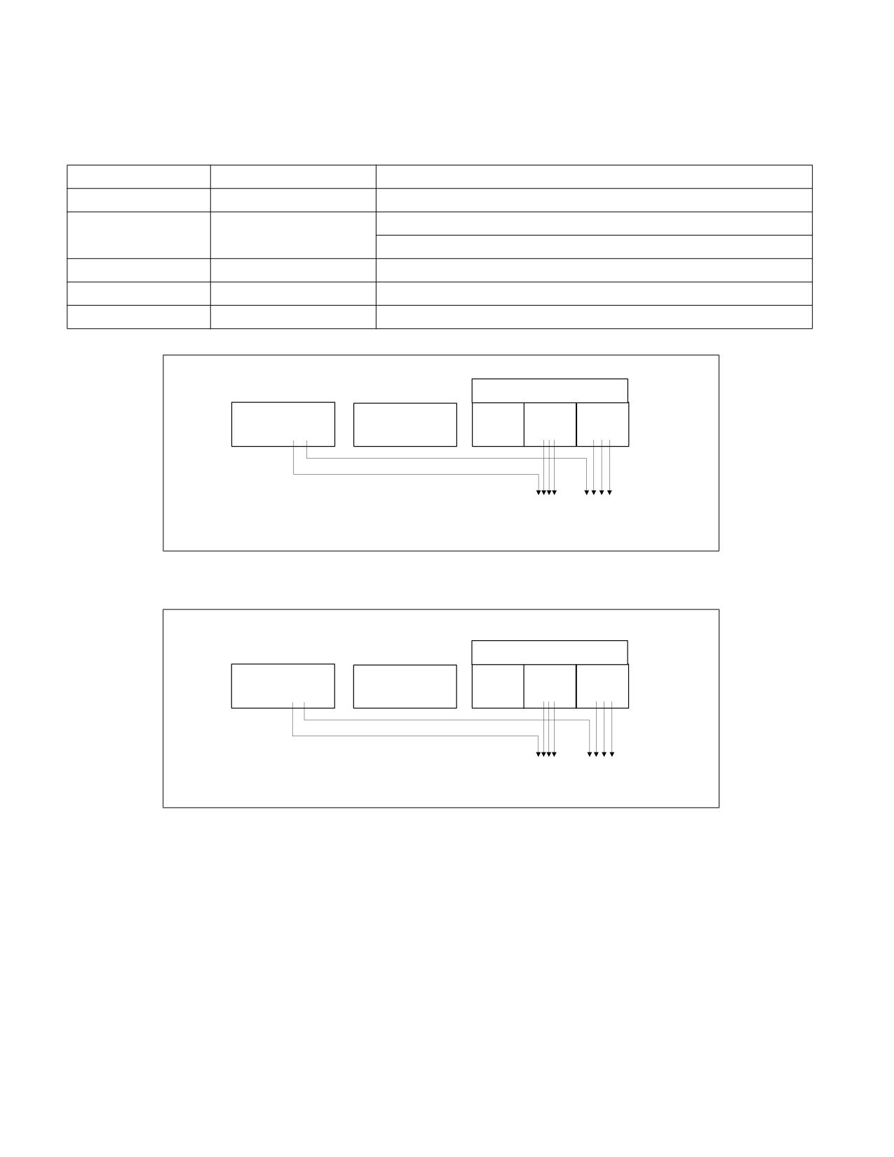
Table 2-4. REX Prefix Fields [BITS: 0100WRXB]
Field Name
Bit Position
Definition
-
7:4
0100
W
3
0 = Operand size determined by CS.D
1 = 64 Bit Operand Size
R
2
Extension of the ModR/M reg field
X
1
Extension of the SIB index field
B
0
Extension of the ModR/M r/m field, SIB base field, or Opcode reg field
ModRM Byte
REX PREFIX
Opcode
mod
reg
r/m
0100WR0B
≠11
rrr
bbb
Rrrr
Bbbb
OM17Xfig1-3
Figure 2-4. Memory Addressing Without an SIB Byte; REX.X Not Used
ModRM Byte
REX PREFIX
Opcode
mod
reg
r/m
0100WR0B
11
rrr
bbb
Rrrr
Bbbb
OM17Xfig1-4
Figure 2-5. Register-Register Addressing (No Memory Operand); REX.X Not Used
Vol. 2A
2-9
INSTRUCTION FORMAT
ModRM Byte
SIB Byte
REX PREFIX
Opcode
mod
reg
r/m
scale
index
base
0100WRXB
≠ 11
rrr
100
ss
xxx
bbb
Rrrr
Xxxx
Bbbb
OM17Xfig1-5
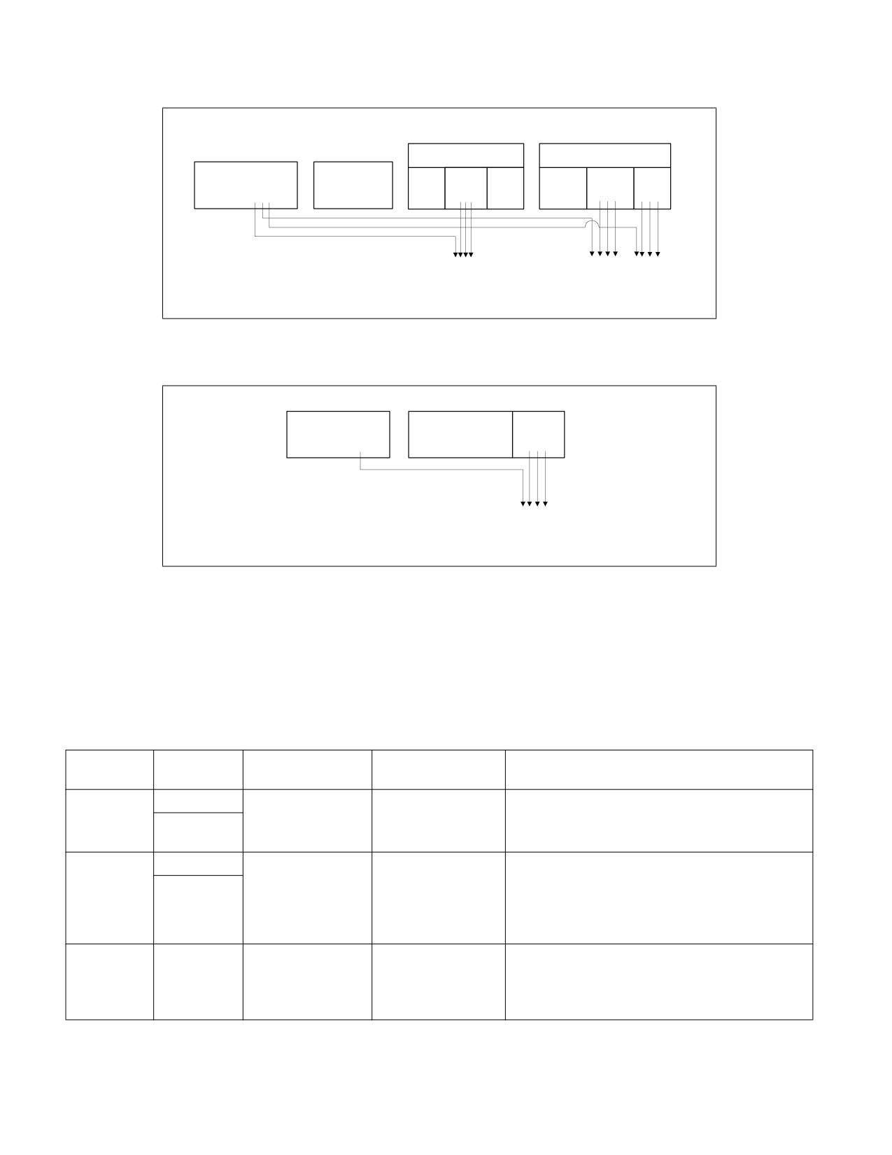
Figure 2-6. Memory Addressing With a SIB Byte
REX PREFIX
Opcode
reg
0100W00B
bbb
Bbbb
OM17Xfig1-6
Figure 2-7. Register Operand Coded in Opcode Byte; REX.X & REX.R Not Used
In the IA-32 architecture, byte registers (AH, AL, BH, BL, CH, CL, DH, and DL) are encoded in the ModR/M byte’s
reg field, the r/m field or the opcode reg field as registers 0 through 7. REX prefixes provide an additional
addressing capability for byte-registers that makes the least-significant byte of GPRs available for byte operations.
Certain combinations of the fields of the ModR/M byte and the SIB byte have special meaning for register encod-
ings. For some combinations, fields expanded by the REX prefix are not decoded. Table 2-5 describes how each
case behaves.
Table 2-5. Special Cases of REX Encodings
ModR/M or
Sub-field
Compatibility Mode
Compatibility Mode
Additional Implications
SIB
Encodings
Operation
Implications
ModR/M Byte
mod ? 11
SIB byte present.
SIB byte required for
REX prefix adds a fourth bit (b) which is not decoded
ESP-based
(don't care).
r/m =
addressing.
b*100(ESP)
SIB byte also required for R12-based addressing.
ModR/M Byte
mod = 0
Base register not
EBP without a
REX prefix adds a fourth bit (b) which is not decoded
used.
displacement must be
(don't care).
r/m =
done using
b*101(EBP)
Using RBP or R13 without displacement must be
mod = 01 with
done using mod = 01 with a displacement of 0.
displacement of 0.
SIB Byte
index =
Index register not
ESP cannot be used
REX prefix adds a fourth bit (b) which is decoded.
0100(ESP)
used.
as an index register.
There are no additional implications. The expanded
index field allows distinguishing RSP from R12,
therefore R12 can be used as an index.
2-10
Vol. 2A

INSTRUCTION FORMAT
Table 2-5. Special Cases of REX Encodings (Contd.)
ModR/M or
Sub-field
Compatibility Mode
Compatibility Mode
Additional Implications
SIB
Encodings
Operation
Implications
SIB Byte
base =
Base register is
Base register
REX prefix adds a fourth bit (b) which is not decoded.
0101(EBP)
unused if mod = 0.
depends on mod
This requires explicit displacement to be used with
encoding.
EBP/RBP or R13.
NOTES:
* Don’t care about value of REX.B
2.2.1.3
Displacement
Addressing in 64-bit mode uses existing 32-bit ModR/M and SIB encodings. The ModR/M and SIB displacement
sizes do not change. They remain 8 bits or 32 bits and are sign-extended to 64 bits.
2.2.1.4
Direct Memory-Offset MOVs
In 64-bit mode, direct memory-offset forms of the MOV instruction are extended to specify a 64-bit immediate
absolute address. This address is called a moffset. No prefix is needed to specify this 64-bit memory offset. For
these MOV instructions, the size of the memory offset follows the address-size default (64 bits in 64-bit mode). See
Table 2-6.
Table 2-6. Direct Memory Offset Form of MOV
Opcode
Instruction
A0
MOV AL, moffset
A1
MOV EAX, moffset
A2
MOV moffset, AL
A3
MOV moffset, EAX
2.2.1.5
Immediates
In 64-bit mode, the typical size of immediate operands remains 32 bits. When the operand size is 64 bits, the
processor sign-extends all immediates to 64 bits prior to their use.
Support for 64-bit immediate operands is accomplished by expanding the semantics of the existing move (MOV
reg, imm16/32) instructions. These instructions (opcodes B8H - BFH) move 16-bits or 32-bits of immediate data
(depending on the effective operand size) into a GPR. When the effective operand size is 64 bits, these instructions
can be used to load an immediate into a GPR. A REX prefix is needed to override the 32-bit default operand size to
a 64-bit operand size.
For example:
48 B8
8877665544332211 MOV RAX,1122334455667788H
2.2.1.6
RIP-Relative Addressing
A new addressing form, RIP-relative (relative instruction-pointer) addressing, is implemented in 64-bit mode. An
effective address is formed by adding displacement to the 64-bit RIP of the next instruction.
In IA-32 architecture and compatibility mode, addressing relative to the instruction pointer is available only with
control-transfer instructions. In 64-bit mode, instructions that use ModR/M addressing can use RIP-relative
addressing. Without RIP-relative addressing, all ModR/M modes address memory relative to zero.
RIP-relative addressing allows specific ModR/M modes to address memory relative to the 64-bit RIP using a signed
32-bit displacement. This provides an offset range of ±2GB from the RIP. Table 2-7 shows the ModR/M and SIB
encodings for RIP-relative addressing. Redundant forms of 32-bit displacement-addressing exist in the current
ModR/M and SIB encodings. There is one ModR/M encoding and there are several SIB encodings. RIP-relative
addressing is encoded using a redundant form.
Vol. 2A
2-11

INSTRUCTION FORMAT
In 64-bit mode, the ModR/M Disp32 (32-bit displacement) encoding is re-defined to be RIP+Disp32 rather than
displacement-only. See Table 2-7.
Table 2-7. RIP-Relative Addressing
Compatibility Mode
64-bit Mode
ModR/M and SIB Sub-field Encodings
Additional Implications in 64-bit mode
Operation
Operation
ModR/M Byte
mod = 00
Disp32
RIP + Disp32
In 64-bit mode, if one wants to use a Disp32
without specifying a base register, one can use a
r/m = 101 (none)
SIB byte encoding (indicated by ModR/M.r/m=100)
as described in the next row.
SIB Byte
base = 101 (none)
If mod = 00, Disp32
Same as legacy
None
index = 100 (none)
scale = 0, 1, 2, 4
The ModR/M encoding for RIP-relative addressing does not depend on using a prefix. Specifically, the r/m bit field
encoding of 101B (used to select RIP-relative addressing) is not affected by the REX prefix. For example, selecting
R13 (REX.B = 1, r/m = 101B) with mod = 00B still results in RIP-relative addressing. The 4-bit r/m field of REX.B
combined with ModR/M is not fully decoded. In order to address R13 with no displacement, software must encode
R13 + 0 using a 1-byte displacement of zero.
RIP-relative addressing is enabled by 64-bit mode, not by a 64-bit address-size. The use of the address-size prefix
does not disable RIP-relative addressing. The effect of the address-size prefix is to truncate and zero-extend the
computed effective address to 32 bits.
2.2.1.7
Default 64-Bit Operand Size
In 64-bit mode, two groups of instructions have a default operand size of 64 bits (do not need a REX prefix for this
operand size). These are:
• Near branches.
• All instructions, except far branches, that implicitly reference the RSP.
2.2.2
Additional Encodings for Control and Debug Registers
In 64-bit mode, more encodings for control and debug registers are available. The REX.R bit is used to modify the
ModR/M reg field when that field encodes a control or debug register (see Table 2-4). These encodings enable the
processor to address CR8-CR15 and DR8- DR15. An additional control register (CR8) is defined in 64-bit mode. CR8
becomes the Task Priority Register (TPR).
In the first implementation of IA-32e mode, CR9-CR15 and DR8-DR15 are not implemented. Any attempt to access
unimplemented registers results in an invalid-opcode exception (#UD).
2.3
INTEL® ADVANCED VECTOR EXTENSIONS (INTEL® AVX)
Intel AVX instructions are encoded using an encoding scheme that combines prefix bytes, opcode extension field,
operand encoding fields, and vector length encoding capability into a new prefix, referred to as VEX. In the VEX
encoding scheme, the VEX prefix may be two or three bytes long, depending on the instruction semantics. Despite
the two-byte or three-byte length of the VEX prefix, the VEX encoding format provides a more compact represen-
tation/packing of the components of encoding an instruction in Intel 64 architecture. The VEX encoding scheme
also allows more headroom for future growth of Intel 64 architecture.
2.3.1
Instruction Format
Instruction encoding using VEX prefix provides several advantages:
2-12
Vol. 2A

INSTRUCTION FORMAT
• Instruction syntax support for three operands and up-to four operands when necessary. For example, the third
source register used by VBLENDVPD is encoded using bits 7:4 of the immediate byte.
• Encoding support for vector length of 128 bits (using XMM registers) and 256 bits (using YMM registers).
• Encoding support for instruction syntax of non-destructive source operands.
• Elimination of escape opcode byte (0FH), SIMD prefix byte (66H, F2H, F3H) via a compact bit field represen-
tation within the VEX prefix.
• Elimination of the need to use REX prefix to encode the extended half of general-purpose register sets (R8-
R15) for direct register access, memory addressing, or accessing XMM8-XMM15 (including YMM8-YMM15).
• Flexible and more compact bit fields are provided in the VEX prefix to retain the full functionality provided by
REX prefix. REX.W, REX.X, REX.B functionalities are provided in the three-byte VEX prefix only because only a
subset of SIMD instructions need them.
• Extensibility for future instruction extensions without significant instruction length increase.
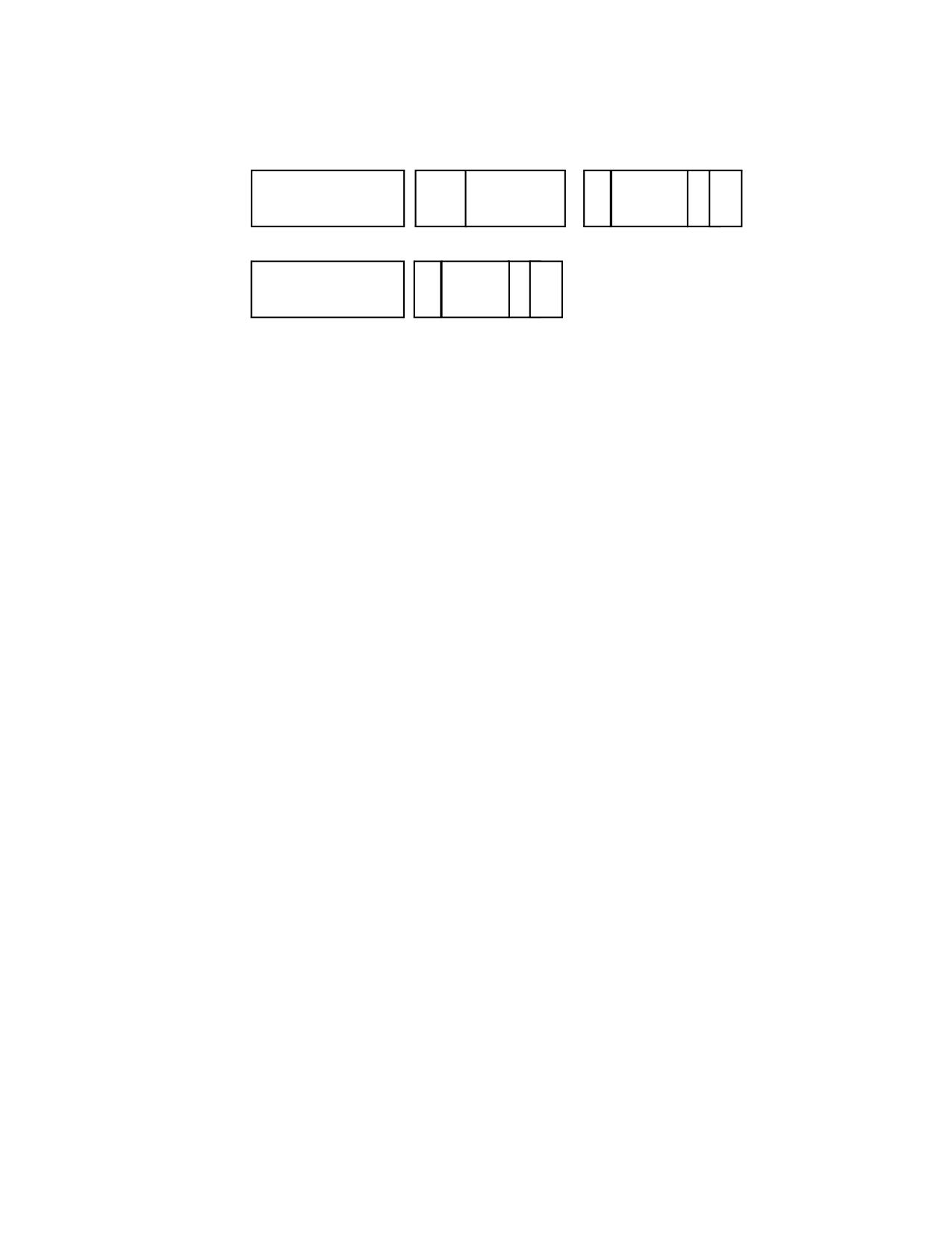
Figure 2-8 shows the Intel 64 instruction encoding format with VEX prefix support. Legacy instruction without a
VEX prefix is fully supported and unchanged. The use of VEX prefix in an Intel 64 instruction is optional, but a VEX
prefix is required for Intel 64 instructions that operate on YMM registers or support three and four operand syntax.
VEX prefix is not a constant-valued, “single-purpose” byte like 0FH, 66H, F2H, F3H in legacy SSE instructions. VEX
prefix provides substantially richer capability than the REX prefix.
# Bytes
2,3
1
1
0,1
0,1,2,4
0,1
[Prefixes]
[VEX]
OPCODE
ModR/M
[SIB]
[DISP]
[IMM]
Figure 2-8. Instruction Encoding Format with VEX Prefix
2.3.2
VEX and the LOCK prefix
Any VEX-encoded instruction with a LOCK prefix preceding VEX will #UD.
2.3.3
VEX and the 66H, F2H, and F3H prefixes
Any VEX-encoded instruction with a 66H, F2H, or F3H prefix preceding VEX will #UD.
2.3.4
VEX and the REX prefix
Any VEX-encoded instruction with a REX prefix proceeding VEX will #UD.
2.3.5
The VEX Prefix
The VEX prefix is encoded in either the two-byte form (the first byte must be C5H) or in the three-byte form (the
first byte must be C4H). The two-byte VEX is used mainly for 128-bit, scalar, and the most common 256-bit AVX
instructions; while the three-byte VEX provides a compact replacement of REX and 3-byte opcode instructions
(including AVX and FMA instructions). Beyond the first byte of the VEX prefix, it consists of a number of bit fields
providing specific capability, they are shown in Figure 2-9.
The bit fields of the VEX prefix can be summarized by its functional purposes:
• Non-destructive source register encoding (applicable to three and four operand syntax): This is the first source
operand in the instruction syntax. It is represented by the notation, VEX.vvvv. This field is encoded using 1’s
complement form (inverted form), i.e., XMM0/YMM0/R0 is encoded as 1111B, XMM15/YMM15/R15 is encoded
as 0000B.
Vol. 2A
2-13
INSTRUCTION FORMAT
• Vector length encoding: This 1-bit field represented by the notation VEX.L. L= 0 means vector length is 128 bits
wide, L=1 means 256 bit vector. The value of this field is written as VEX.128 or VEX.256 in this document to
distinguish encoded values of other VEX bit fields.
• REX prefix functionality: Full REX prefix functionality is provided in the three-byte form of VEX prefix. However
the VEX bit fields providing REX functionality are encoded using 1’s complement form, i.e., XMM0/YMM0/R0 is
encoded as 1111B, XMM15/YMM15/R15 is encoded as 0000B.
- Two-byte form of the VEX prefix only provides the equivalent functionality of REX.R, using 1’s complement
encoding. This is represented as VEX.R.
- Three-byte form of the VEX prefix provides REX.R, REX.X, REX.B functionality using 1’s complement
encoding and three dedicated bit fields represented as VEX.R, VEX.X, VEX.B.
- Three-byte form of the VEX prefix provides the functionality of REX.W only to specific instructions that need
to override default 32-bit operand size for a general purpose register to 64-bit size in 64-bit mode. For
those applicable instructions, VEX.W field provides the same functionality as REX.W. VEX.W field can
provide completely different functionality for other instructions.
Consequently, the use of REX prefix with VEX encoded instructions is not allowed. However, the intent of the
REX prefix for expanding register set is reserved for future instruction set extensions using VEX prefix
encoding format.
• Compaction of SIMD prefix: Legacy SSE instructions effectively use SIMD prefixes (66H, F2H, F3H) as an
opcode extension field. VEX prefix encoding allows the functional capability of such legacy SSE instructions
(operating on XMM registers, bits 255:128 of corresponding YMM unmodified) to be encoded using the VEX.pp
field without the presence of any SIMD prefix. The VEX-encoded 128-bit instruction will zero-out bits 255:128
of the destination register. VEX-encoded instruction may have 128 bit vector length or 256 bits length.
• Compaction of two-byte and three-byte opcode: More recently introduced legacy SSE instructions employ two
and three-byte opcode. The one or two leading bytes are: 0FH, and 0FH 3AH/0FH 38H. The one-byte escape
(0FH) and two-byte escape (0FH 3AH, 0FH 38H) can also be interpreted as an opcode extension field. The
VEX.mmmmm field provides compaction to allow many legacy instruction to be encoded without the constant
byte sequence, 0FH, 0FH 3AH, 0FH 38H. These VEX-encoded instruction may have 128 bit vector length or 256
bits length.
The VEX prefix is required to be the last prefix and immediately precedes the opcode bytes. It must follow any other
prefixes. If VEX prefix is present a REX prefix is not supported.
The 3-byte VEX leaves room for future expansion with 3 reserved bits. REX and the 66h/F2h/F3h prefixes are
reclaimed for future use.
VEX prefix has a two-byte form and a three byte form. If an instruction syntax can be encoded using the two-byte
form, it can also be encoded using the three byte form of VEX. The latter increases the length of the instruction by
one byte. This may be helpful in some situations for code alignment.
The VEX prefix supports 256-bit versions of floating-point SSE, SSE2, SSE3, and SSE4 instructions. Note, certain
new instruction functionality can only be encoded with the VEX prefix.
The VEX prefix will #UD on any instruction containing MMX register sources or destinations.
2-14
Vol. 2A
INSTRUCTION FORMAT
Byte 0
Byte 1
Byte 2
(Bit Position) 7
0
7
6
5
4
0
7
6
3
2
1
0
3-byte VEX
11000100
R X B
m-mmmm
W
vvvv
L
pp
7
0
7
6
3
2
1
0
2-byte VEX
11000101
R
vvvv
L
pp
R: REX.R in 1’s complement (inverted) form
1: Same as REX.R=0 (must be 1 in 32-bit mode)
0: Same as REX.R=1 (64-bit mode only)
X: REX.X in 1’s complement (inverted) form
1: Same as REX.X=0 (must be 1 in 32-bit mode)
0: Same as REX.X=1 (64-bit mode only)
B: REX.B in 1’s complement (inverted) form
1: Same as REX.B=0 (Ignored in 32-bit mode).
0: Same as REX.B=1 (64-bit mode only)
W: opcode specific (use like REX.W, or used for opcode
extension, or ignored, depending on the opcode byte)
m-mmmm:
00000: Reserved for future use (will #UD)
00001: implied 0F leading opcode byte
00010: implied 0F 38 leading opcode bytes
00011: implied 0F 3A leading opcode bytes
00100-11111: Reserved for future use (will #UD)
vvvv: a register specifier (in 1’s complement form) or 1111 if unused.
L: Vector Length
0: scalar or 128-bit vector
1: 256-bit vector
pp: opcode extension providing equivalent functionality of a SIMD prefix
00: None
01: 66
10: F3
11: F2
Figure 2-9. VEX bit fields
The following subsections describe the various fields in two or three-byte VEX prefix.
2.3.5.1
VEX Byte 0, bits[7:0]
VEX Byte 0, bits [7:0] must contain the value 11000101b (C5h) or 11000100b (C4h). The 3-byte VEX uses the C4h
first byte, while the 2-byte VEX uses the C5h first byte.
2.3.5.2
VEX Byte 1, bit [7] - ‘R’
VEX Byte 1, bit [7] contains a bit analogous to a bit inverted REX.R. In protected and compatibility modes the bit
must be set to ‘1’ otherwise the instruction is LES or LDS.
Vol. 2A
2-15
INSTRUCTION FORMAT
This bit is present in both 2- and 3-byte VEX prefixes.
The usage of WRXB bits for legacy instructions is explained in detail section 2.2.1.2 of Intel 64 and IA-32 Architec-
tures Software developer’s manual, Volume 2A.
This bit is stored in bit inverted format.
2.3.5.3
3-byte VEX byte 1, bit[6] - ‘X’
Bit[6] of the 3-byte VEX byte 1 encodes a bit analogous to a bit inverted REX.X. It is an extension of the SIB Index
field in 64-bit modes. In 32-bit modes, this bit must be set to ‘1’ otherwise the instruction is LES or LDS.
This bit is available only in the 3-byte VEX prefix.
This bit is stored in bit inverted format.
2.3.5.4
3-byte VEX byte 1, bit[5] - ‘B’
Bit[5] of the 3-byte VEX byte 1 encodes a bit analogous to a bit inverted REX.B. In 64-bit modes, it is an extension
of the ModR/M r/m field, or the SIB base field. In 32-bit modes, this bit is ignored.
This bit is available only in the 3-byte VEX prefix.
This bit is stored in bit inverted format.
2.3.5.5
3-byte VEX byte 2, bit[7] - ‘W’
Bit[7] of the 3-byte VEX byte 2 is represented by the notation VEX.W. It can provide following functions, depending
on the specific opcode.
• For AVX instructions that have equivalent legacy SSE instructions (typically these SSE instructions have a
general-purpose register operand with its operand size attribute promotable by REX.W), if REX.W promotes
the operand size attribute of the general-purpose register operand in legacy SSE instruction, VEX.W has same
meaning in the corresponding AVX equivalent form. In 32-bit modes for these instructions, VEX.W is silently
ignored.
• For AVX instructions that have equivalent legacy SSE instructions (typically these SSE instructions have oper-
ands with their operand size attribute fixed and not promotable by REX.W), if REX.W is don’t care in legacy
SSE instruction, VEX.W is ignored in the corresponding AVX equivalent form irrespective of mode.
• For new AVX instructions where VEX.W has no defined function (typically these meant the combination of the
opcode byte and VEX.mmmmm did not have any equivalent SSE functions), VEX.W is reserved as zero and
setting to other than zero will cause instruction to #UD.
2.3.5.6
2-byte VEX Byte 1, bits[6:3] and 3-byte VEX Byte 2, bits [6:3]- ‘vvvv’ the Source or Dest
Register Specifier
In 32-bit mode the VEX first byte C4 and C5 alias onto the LES and LDS instructions. To maintain compatibility with
existing programs the VEX 2nd byte, bits [7:6] must be 11b. To achieve this, the VEX payload bits are selected to
place only inverted, 64-bit valid fields (extended register selectors) in these upper bits.
The 2-byte VEX Byte 1, bits [6:3] and the 3-byte VEX, Byte 2, bits [6:3] encode a field (shorthand VEX.vvvv) that
for instructions with 2 or more source registers and an XMM or YMM or memory destination encodes the first source
register specifier stored in inverted (1’s complement) form.
VEX.vvvv is not used by the instructions with one source (except certain shifts, see below) or on instructions with
no XMM or YMM or memory destination. If an instruction does not use VEX.vvvv then it should be set to 1111b
otherwise instruction will #UD.
In 64-bit mode all 4 bits may be used. See Table for the encoding of the XMM or YMM registers. In 32-bit and 16-
bit modes bit 6 must be 1 (if bit 6 is not 1, the 2-byte VEX version will generate LDS instruction and the 3-byte VEX
version will ignore this bit).
2-16
Vol. 2A
INSTRUCTION FORMAT
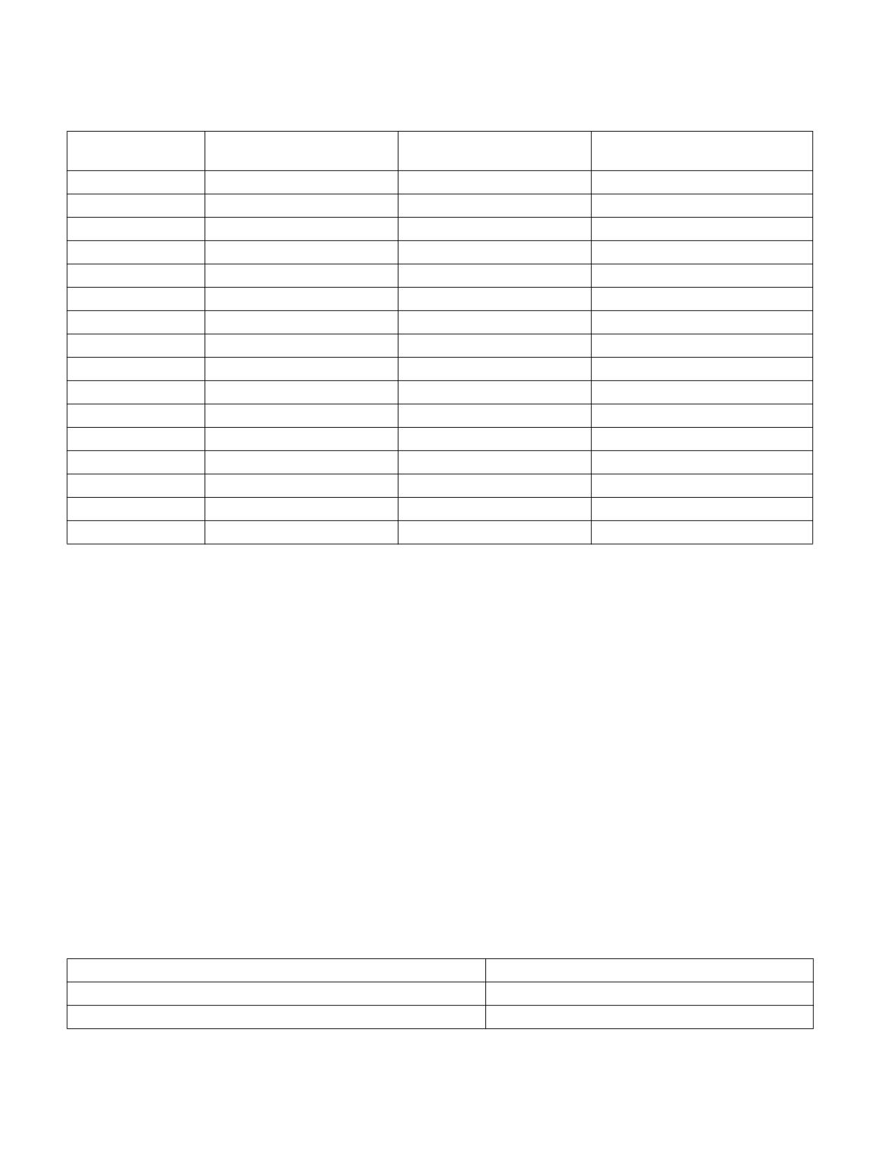
Table 2-8. VEX.vvvv to Register Name Mapping
General-Purpose Register (If
Valid in Legacy/Compatibility 32-bit
VEX.vvvv
Dest Register
Applicable)1
modes?2
1111B
XMM0/YMM0
RAX/EAX
Valid
1110B
XMM1/YMM1
RCX/ECX
Valid
1101B
XMM2/YMM2
RDX/EDX
Valid
1100B
XMM3/YMM3
RBX/EBX
Valid
1011B
XMM4/YMM4
RSP/ESP
Valid
1010B
XMM5/YMM5
RBP/EBP
Valid
1001B
XMM6/YMM6
RSI/ESI
Valid
1000B
XMM7/YMM7
RDI/EDI
Valid
0111B
XMM8/YMM8
R8/R8D
Invalid
0110B
XMM9/YMM9
R9/R9D
Invalid
0101B
XMM10/YMM10
R10/R10D
Invalid
0100B
XMM11/YMM11
R11/R11D
Invalid
0011B
XMM12/YMM12
R12/R12D
Invalid
0010B
XMM13/YMM13
R13/R13D
Invalid
0001B
XMM14/YMM14
R14/R14D
Invalid
0000B
XMM15/YMM15
R15/R15D
Invalid
NOTES:
1. See Section 2.6, “VEX Encoding Support for GPR Instructions” for additional details.
2. Only the first eight General-Purpose Registers are accessible/encodable in 16/32b modes.
The VEX.vvvv field is encoded in bit inverted format for accessing a register operand.
2.3.6
Instruction Operand Encoding and VEX.vvvv, ModR/M
VEX-encoded instructions support three-operand and four-operand instruction syntax. Some VEX-encoded
instructions have syntax with less than three operands, e.g., VEX-encoded pack shift instructions support one
source operand and one destination operand).
The roles of VEX.vvvv, reg field of ModR/M byte (ModR/M.reg), r/m field of ModR/M byte (ModR/M.r/m) with
respect to encoding destination and source operands vary with different type of instruction syntax.
The role of VEX.vvvv can be summarized to three situations:
• VEX.vvvv encodes the first source register operand, specified in inverted (1’s complement) form and is valid for
instructions with 2 or more source operands.
• VEX.vvvv encodes the destination register operand, specified in 1’s complement form for certain vector shifts.
The instructions where VEX.vvvv is used as a destination are listed in Table 2-9. The notation in the “Opcode”
column in Table 2-9 is described in detail in section 3.1.1.
• VEX.vvvv does not encode any operand, the field is reserved and should contain 1111b.
Table 2-9. Instructions with a VEX.vvvv Destination
Opcode
Instruction mnemonic
VEX.128.66.0F 73 /7 ib
VPSLLDQ xmm1, xmm2, imm8
VEX.128.66.0F 73 /3 ib
VPSRLDQ xmm1, xmm2, imm8
Vol. 2A
2-17
INSTRUCTION FORMAT
Table 2-9. Instructions with a VEX.vvvv Destination (Contd.)
Opcode
Instruction mnemonic
VEX.128.66.0F 71 /2 ib
VPSRLW xmm1, xmm2, imm8
VEX.128.66.0F 72 /2 ib
VPSRLD xmm1, xmm2, imm8
VEX.128.66.0F 73 /2 ib
VPSRLQ xmm1, xmm2, imm8
VEX.128.66.0F 71 /4 ib
VPSRAW xmm1, xmm2, imm8
VEX.128.66.0F 72 /4 ib
VPSRAD xmm1, xmm2, imm8
VEX.128.66.0F 71 /6 ib
VPSLLW xmm1, xmm2, imm8
VEX.128.66.0F 72 /6 ib
VPSLLD xmm1, xmm2, imm8
VEX.128.66.0F 73 /6 ib
VPSLLQ xmm1, xmm2, imm8
The role of ModR/M.r/m field can be summarized to two situations:
• ModR/M.r/m encodes the instruction operand that references a memory address.
• For some instructions that do not support memory addressing semantics, ModR/M.r/m encodes either the
destination register operand or a source register operand.
The role of ModR/M.reg field can be summarized to two situations:
• ModR/M.reg encodes either the destination register operand or a source register operand.
• For some instructions, ModR/M.reg is treated as an opcode extension and not used to encode any instruction
operand.
For instruction syntax that support four operands, VEX.vvvv, ModR/M.r/m, ModR/M.reg encodes three of the four
operands. The role of bits 7:4 of the immediate byte serves the following situation:
• Imm8[7:4] encodes the third source register operand.
2.3.6.1
3-byte VEX byte 1, bits[4:0] - “m-mmmm”
Bits[4:0] of the 3-byte VEX byte 1 encode an implied leading opcode byte (0F, 0F 38, or 0F 3A). Several bits are
reserved for future use and will #UD unless 0.
Table 2-10. VEX.m-mmmm Interpretation
VEX.m-mmmm
Implied Leading Opcode Bytes
00000B
Reserved
00001B
0F
00010B
0F 38
00011B
0F 3A
00100-11111B
Reserved
(2-byte VEX)
0F
VEX.m-mmmm is only available on the 3-byte VEX. The 2-byte VEX implies a leading 0Fh opcode byte.
2.3.6.2
2-byte VEX byte 1, bit[2], and 3-byte VEX byte 2, bit [2]- “L”
The vector length field, VEX.L, is encoded in bit[2] of either the second byte of 2-byte VEX, or the third byte of 3-
byte VEX. If “VEX.L = 1”, it indicates 256-bit vector operation. “VEX.L = 0” indicates scalar and 128-bit vector
operations.
The instruction VZEROUPPER is a special case that is encoded with VEX.L = 0, although its operation zero’s bits
255:128 of all YMM registers accessible in the current operating mode. See Table 2-11.
2-18
Vol. 2A
INSTRUCTION FORMAT
Table 2-11. VEX.L Interpretation
VEX.L
Vector Length
0
128-bit (or 32/64-bit scalar)
1
256-bit
2.3.6.3
2-byte VEX byte 1, bits[1:0], and 3-byte VEX byte 2, bits [1:0]- “pp”
Up to one implied prefix is encoded by bits[1:0] of either the 2-byte VEX byte 1 or the 3-byte VEX byte 2. The prefix
behaves as if it was encoded prior to VEX, but after all other encoded prefixes. See Table 2-12.
Table 2-12. VEX.pp Interpretation
pp
Implies this prefix after other prefixes but before VEX
00B
None
01B
66
10B
F3
11B
F2
2.3.7
The Opcode Byte
One (and only one) opcode byte follows the 2 or 3 byte VEX. Legal opcodes are specified in Appendix B, in color.
Any instruction that uses illegal opcode will #UD.
2.3.8
The ModR/M, SIB, and Displacement Bytes
The encodings are unchanged but the interpretation of reg_field or rm_field differs (see above).
2.3.9
The Third Source Operand (Immediate Byte)
VEX-encoded instructions can support instruction with a four operand syntax. VBLENDVPD, VBLENDVPS, and
PBLENDVB use imm8[7:4] to encode one of the source registers.
2.3.10 Intel® AVX Instructions and the Upper 128-bits of YMM registers
If an instruction with a destination XMM register is encoded with a VEX prefix, the processor zeroes the upper bits
(above bit 128) of the equivalent YMM register. Legacy SSE instructions without VEX preserve the upper bits.
2.3.10.1 Vector Length Transition and Programming Considerations
An instruction encoded with a VEX.128 prefix that loads a YMM register operand operates as follows:
• Data is loaded into bits 127:0 of the register
• Bits above bit 127 in the register are cleared.
Thus, such an instruction clears bits 255:128 of a destination YMM register on processors with a maximum vector-
register width of 256 bits. In the event that future processors extend the vector registers to greater widths, an
instruction encoded with a VEX.128 or VEX.256 prefix will also clear any bits beyond bit 255. (This is in contrast
with legacy SSE instructions, which have no VEX prefix; these modify only bits 127:0 of any destination register
operand.)
Programmers should bear in mind that instructions encoded with VEX.128 and VEX.256 prefixes will clear any
future extensions to the vector registers. A calling function that uses such extensions should save their state before
calling legacy functions. This is not possible for involuntary calls (e.g., into an interrupt-service routine). It is
Vol. 2A
2-19
INSTRUCTION FORMAT
recommended that software handling involuntary calls accommodate this by not executing instructions encoded
with VEX.128 and VEX.256 prefixes. In the event that it is not possible or desirable to restrict these instructions,
then software must take special care to avoid actions that would, on future processors, zero the upper bits of vector
registers.
Processors that support further vector-register extensions (defining bits beyond bit 255) will also extend the
XSAVE and XRSTOR instructions to save and restore these extensions. To ensure forward compatibility, software
that handles involuntary calls and that uses instructions encoded with VEX.128 and VEX.256 prefixes should first
save and then restore the vector registers (with any extensions) using the XSAVE and XRSTOR instructions with
save/restore masks that set bits that correspond to all vector-register extensions. Ideally, software should rely on
a mechanism that is cognizant of which bits to set. (E.g., an OS mechanism that sets the save/restore mask bits
for all vector-register extensions that are enabled in XCR0.) Saving and restoring state with instructions other than
XSAVE and XRSTOR will, on future processors with wider vector registers, corrupt the extended state of the vector
registers - even if doing so functions correctly on processors supporting 256-bit vector registers. (The same is true
if XSAVE and XRSTOR are used with a save/restore mask that does not set bits corresponding to all supported
extensions to the vector registers.)
2.3.11 Intel® AVX Instruction Length
The Intel AVX instructions described in this document (including VEX and ignoring other prefixes) do not exceed 11
bytes in length, but may increase in the future. The maximum length of an Intel 64 and IA-32 instruction remains
15 bytes.
2.3.12 Vector SIB (VSIB) Memory Addressing
In Intel® Advanced Vector Extensions 2 (Intel® AVX2), an SIB byte that follows the ModR/M byte can support VSIB
memory addressing to an array of linear addresses. VSIB addressing is only supported in a subset of Intel AVX2
instructions. VSIB memory addressing requires 32-bit or 64-bit effective address. In 32-bit mode, VSIB addressing
is not supported when address size attribute is overridden to 16 bits. In 16-bit protected mode, VSIB memory
addressing is permitted if address size attribute is overridden to 32 bits. Additionally, VSIB memory addressing is
supported only with VEX prefix.
In VSIB memory addressing, the SIB byte consists of:
• The scale field (bit 7:6) specifies the scale factor.
• The index field (bits 5:3) specifies the register number of the vector index register, each element in the vector
register specifies an index.
• The base field (bits 2:0) specifies the register number of the base register.
Table 2-13 shows the 32-bit VSIB addressing form. It is organized to give 256 possible values of the SIB byte (in
hexadecimal). General purpose registers used as a base are indicated across the top of the table, along with corre-
sponding values for the SIB byte’s base field. The register names also include R8D-R15D applicable only in 64-bit
mode (when address size override prefix is used, but the value of VEX.B is not shown in Table 2-13). In 32-bit
mode, R8D-R15D does not apply.
Table rows in the body of the table indicate the vector index register used as the index field and each supported
scaling factor shown separately. Vector registers used in the index field can be XMM or YMM registers. The left-
most column includes vector registers VR8-VR15 (i.e., XMM8/YMM8-XMM15/YMM15), which are only available in
64-bit mode and does not apply if encoding in 32-bit mode.
2-20
Vol. 2A

INSTRUCTION FORMAT
Table 2-13. 32-Bit VSIB Addressing Forms of the SIB Byte
r32
EAX/
ECX/
EDX/
EBX/
ESP/
EBP/
ESI/
EDI/
R8D
R9D
R10D
R11D
R12D
R13D1
R14D
R15D
(In decimal) Base =
0
1
2
3
4
5
6
7
(In binary) Base =
000
001
010
011
100
101
110
111
Scaled Index
SS
Index
Value of SIB Byte (in Hexadecimal)
VR0/VR8
*1
00
000
00
01
02
03
04
05
06
07
VR1/VR9
001
08
09
0A
0B
0C
0D
0E
0F
VR2/VR10
010
10
11
12
13
14
15
16
17
VR3/VR11
011
18
19
1A
1B
1C
1D
1E
1F
VR4/VR12
100
20
21
22
23
24
25
26
27
VR5/VR13
101
28
29
2A
2B
2C
2D
2E
2F
VR6/VR14
110
30
31
32
33
34
35
36
37
VR7/VR15
111
38
39
3A
3B
3C
3D
3E
3F
VR0/VR8
*2
01
000
40
41
42
43
44
45
46
47
VR1/VR9
001
48
49
4A
4B
4C
4D
4E
4F
VR2/VR10
010
50
51
52
53
54
55
56
57
VR3/VR11
011
58
59
5A
5B
5C
5D
5E
5F
VR4/VR12
100
60
61
62
63
64
65
66
67
VR5/VR13
101
68
69
6A
6B
6C
6D
6E
6F
VR6/VR14
110
70
71
72
73
74
75
76
77
VR7/VR15
111
78
79
7A
7B
7C
7D
7E
7F
VR0/VR8
*4
10
000
80
81
82
83
84
85
86
87
VR1/VR9
001
88
89
8A
8B
8C
8D
8E
8F
VR2/VR10
010
90
91
92
93
94
95
96
97
VR3/VR11
011
98
89
9A
9B
9C
9D
9E
9F
VR4/VR12
100
A0
A1
A2
A3
A4
A5
A6
A7
VR5/VR13
101
A8
A9
AA
AB
AC
AD
AE
AF
VR6/VR14
110
B0
B1
B2
B3
B4
B5
B6
B7
VR7/VR15
111
B8
B9
BA
BB
BC
BD
BE
BF
VR0/VR8
*8
11
000
C0
C1
C2
C3
C4
C5
C6
C7
VR1/VR9
001
C8
C9
CA
CB
CC
CD
CE
CF
VR2/VR10
010
D0
D1
D2
D3
D4
D5
D6
D7
VR3/VR11
011
D8
D9
DA
DB
DC
DD
DE
DF
VR4/VR12
100
E0
E1
E2
E3
E4
E5
E6
E7
VR5/VR13
101
E8
E9
EA
EB
EC
ED
EE
EF
VR6/VR14
110
F0
F1
F2
F3
F4
F5
F6
F7
VR7/VR15
111
F8
F9
FA
FB
FC
FD
FE
FF
NOTES:
1. If ModR/M.mod = 00b, the base address is zero, then effective address is computed as [scaled vector index] + disp32. Otherwise the
base address is computed as [EBP/R13]+ disp, the displacement is either 8 bit or 32 bit depending on the value of ModR/M.mod:
MOD
Effective Address
00b
[Scaled Vector Register] + Disp32
01b
[Scaled Vector Register] + Disp8 + [EBP/R13]
10b
[Scaled Vector Register] + Disp32 + [EBP/R13]
2.3.12.1
64-bit Mode VSIB Memory Addressing
In 64-bit mode VSIB memory addressing uses the VEX.B field and the base field of the SIB byte to encode one of
the 16 general-purpose register as the base register. The VEX.X field and the index field of the SIB byte encode one
of the 16 vector registers as the vector index register.
In 64-bit mode the top row of Table 2-13 base register should be interpreted as the full 64-bit of each register.
2.4
INTEL® ADVANCED MATRIX EXTENSIONS (INTEL® AMX)
Intel® AMX instructions follow the general documentation convention established in previous sections. Additionally,
Intel® Advanced Matrix Extensions use notation conventions as described below.
In the instruction encoding boxes, sibmem is used to denote an encoding where a ModR/M byte and SIB byte are
used to indicate a memory operation where the base and displacement are used to point to memory, and the index
Vol. 2A
2-21

INSTRUCTION FORMAT
register (if present) is used to denote a stride between memory rows. The index register is scaled by the sib.scale
field as usual. The base register is added to the displacement, if present.
In the instruction encoding, the ModR/M byte is represented several ways depending on the role it plays. The
ModR/M byte has 3 fields: 2-bit ModR/M.mod field, a 3-bit ModR/M.reg field and a 3-bit ModR/M.r/m field. When all
bits of the ModR/M byte have fixed values for an instruction, the 2-hex nibble value of that byte is presented after
the opcode in the encoding boxes on the instruction description pages. When only some fields of the ModR/M byte
must contain fixed values, those values are specified as follows:
• If only the ModR/M.mod must be 0b11, and ModR/M.reg and ModR/M.r/m fields are unrestricted, this is
denoted as 11:rrr:bbb. The rrr correspond to the 3-bits of the ModR/M.reg field and the bbb correspond to the
3-bits of the ModR/M.r/m field.
• If the ModR/M.mod field is constrained to be a value other than 0b11, i.e., it must be one of 0b00, 0b01, or
0b10, then the notation !(11) is used.
• If the ModR/M.reg field had a specific required value, e.g., 0b101, that would be denoted as mm:101:bbb.
NOTE
Historically this document only specified the ModR/M.reg field restrictions with the notation /0 ... /7
and did not specify restrictions on the ModR/M.mod and ModR/M.r/m fields in the encoding boxes.
2.5
INTEL® AVX AND INTEL® SSE INSTRUCTION EXCEPTION CLASSIFICATION
To look up the exceptions of legacy 128-bit SIMD instruction, 128-bit VEX-encoded instructions, and 256-bit VEX-
encoded instruction, Table summarizes the exception behavior into separate classes, with detailed exception
conditions defined in sub-sections 2.5.1 through 2.6.1. For example, ADDPS contains the entry:
“See Exceptions Type 2.”
In this entry, “Type 2” can be looked up in Table 2-19.
The instruction’s corresponding CPUID feature flag can be identified in the fourth column of the Instruction
summary table.
Note: #UD on CPUID feature flags=0 is not guaranteed in a virtualized environment if the hardware supports the
feature flag.
NOTE
Instructions that operate only with MMX, X87, or general-purpose registers are not covered by the
exception classes defined in this section. For instructions that operate on MMX registers, see
Section 25.25.3, “Exception Conditions of Legacy SIMD Instructions Operating on MMX Registers”
in the Intel® 64 and IA-32 Architectures Software Developer’s Manual, Volume 3B.
Table 2-14. Exception Class Description
Floating-Point Exceptions
Exception Class
Instruction Set
Mem Arg
(#XM)
AVX,
Type 1
16/32 byte explicitly aligned
No
Legacy SSE
AVX,
16/32 byte not explicitly
Type 2
Yes
Legacy SSE
aligned
AVX,
Type 3
< 16 byte
Yes
Legacy SSE
AVX,
16/32 byte not explicitly
Type 4
No
Legacy SSE
aligned
AVX,
Type 5
< 16 byte
No
Legacy SSE
Type 6
AVX (no Legacy SSE)
Varies
(At present, none do)
2-22
Vol. 2A

INSTRUCTION FORMAT
Table 2-14. Exception Class Description (Contd.)
Floating-Point Exceptions
Exception Class
Instruction Set
Mem Arg
(#XM)
AVX,
Type 7
None
No
Legacy SSE
Type 8
AVX
None
No
F16C
8 or 16 byte, Not explicitly
Yes
Type 11
aligned, no AC#
Type 12
AVX2 Gathers
Not explicitly aligned, no AC#
No
See Table 2-15 for lists of instructions in each exception class.
Table 2-15. Instructions in Each Exception Class
Exception Class
Instruction
Type 1
(V)MOVAPD, (V)MOVAPS, (V)MOVDQA, (V)MOVNTDQ, (V)MOVNTDQA, (V)MOVNTPD, (V)MOVNTPS
(V)ADDPD, (V)ADDPS, (V)ADDSUBPD, (V)ADDSUBPS, (V)CMPPD, (V)CMPPS, (V)CVTDQ2PS, (V)CVTPD2DQ,
(V)CVTPD2PS, (V)CVTPS2DQ, (V)CVTTPD2DQ, (V)CVTTPS2DQ, (V)DIVPD, (V)DIVPS, (V)DPPD*, (V)DPPS*,
VFMADD132PD, VFMADD213PD, VFMADD231PD, VFMADD132PS, VFMADD213PS, VFMADD231PS,
VFMADDSUB132PD, VFMADDSUB213PD, VFMADDSUB231PD, VFMADDSUB132PS, VFMADDSUB213PS,
VFMADDSUB231PS, VFMSUBADD132PD, VFMSUBADD213PD, VFMSUBADD231PD, VFMSUBADD132PS,
Type 2
VFMSUBADD213PS, VFMSUBADD231PS, VFMSUB132PD, VFMSUB213PD, VFMSUB231PD, VFMSUB132PS,
VFMSUB213PS, VFMSUB231PS, VFNMADD132PD, VFNMADD213PD, VFNMADD231PD, VFNMADD132PS,
VFNMADD213PS, VFNMADD231PS, VFNMSUB132PD, VFNMSUB213PD, VFNMSUB231PD, VFNMSUB132PS,
VFNMSUB213PS, VFNMSUB231PS, (V)HADDPD, (V)HADDPS, (V)HSUBPD, (V)HSUBPS, (V)MAXPD, (V)MAXPS,
(V)MINPD, (V)MINPS, (V)MULPD, (V)MULPS, (V)ROUNDPD, (V)ROUNDPS, (V)SQRTPD, (V)SQRTPS, (V)SUBPD,
(V)SUBPS
(V)ADDSD, (V)ADDSS, (V)CMPSD, (V)CMPSS, (V)COMISD, (V)COMISS, (V)CVTPS2PD, (V)CVTSD2SI, (V)CVTSD2SS,
(V)CVTSI2SD, (V)CVTSI2SS, (V)CVTSS2SD, (V)CVTSS2SI, (V)CVTTSD2SI, (V)CVTTSS2SI, (V)DIVSD, (V)DIVSS,
VFMADD132SD, VFMADD213SD, VFMADD231SD, VFMADD132SS, VFMADD213SS, VFMADD231SS,
VFMSUB132SD, VFMSUB213SD, VFMSUB231SD, VFMSUB132SS, VFMSUB213SS, VFMSUB231SS,
Type 3
VFNMADD132SD, VFNMADD213SD, VFNMADD231SD, VFNMADD132SS, VFNMADD213SS, VFNMADD231SS,
VFNMSUB132SD, VFNMSUB213SD, VFNMSUB231SD, VFNMSUB132SS, VFNMSUB213SS, VFNMSUB231SS,
(V)MAXSD, (V)MAXSS, (V)MINSD, (V)MINSS, (V)MULSD, (V)MULSS, (V)ROUNDSD, (V)ROUNDSS, (V)SQRTSD,
(V)SQRTSS, (V)SUBSD, (V)SUBSS, (V)UCOMISD, (V)UCOMISS
(V)AESDEC, (V)AESDECLAST, (V)AESENC, (V)AESENCLAST, (V)AESIMC, (V)AESKEYGENASSIST, (V)ANDPD,
(V)ANDPS, (V)ANDNPD, (V)ANDNPS, (V)BLENDPD, (V)BLENDPS, VBLENDVPD, VBLENDVPS, (V)LDDQU***,
(V)MASKMOVDQU, (V)PTEST, VTESTPS, VTESTPD, (V)MOVDQU*, (V)MOVSHDUP, (V)MOVSLDUP, (V)MOVUPD*,
(V)MOVUPS*, (V)MPSADBW, (V)ORPD, (V)ORPS, (V)PABSB, (V)PABSW, (V)PABSD, (V)PACKSSWB, (V)PACKSSDW,
(V)PACKUSWB, (V)PACKUSDW, (V)PADDB, (V)PADDW, (V)PADDD, (V)PADDQ, (V)PADDSB, (V)PADDSW,
(V)PADDUSB, (V)PADDUSW, (V)PALIGNR, (V)PAND, (V)PANDN, (V)PAVGB, (V)PAVGW, (V)PBLENDVB, (V)PBLENDW,
(V)PCMP(E/I)STRI/M***, (V)PCMPEQB, (V)PCMPEQW, (V)PCMPEQD, (V)PCMPEQQ, (V)PCMPGTB, (V)PCMPGTW,
(V)PCMPGTD, (V)PCMPGTQ, (V)PCLMULQDQ, (V)PHADDW, (V)PHADDD, (V)PHADDSW, (V)PHMINPOSUW,
(V)PHSUBD, (V)PHSUBW, (V)PHSUBSW, (V)PMADDWD, (V)PMADDUBSW, (V)PMAXSB, (V)PMAXSW, (V)PMAXSD,
Type 4
(V)PMAXUB, (V)PMAXUW, (V)PMAXUD, (V)PMINSB, (V)PMINSW, (V)PMINSD, (V)PMINUB, (V)PMINUW, (V)PMINUD,
(V)PMULHUW, (V)PMULHRSW, (V)PMULHW, (V)PMULLW, (V)PMULLD, (V)PMULUDQ, (V)PMULDQ, (V)POR,
(V)PSADBW, (V)PSHUFB, (V)PSHUFD, (V)PSHUFHW, (V)PSHUFLW, (V)PSIGNB, (V)PSIGNW, (V)PSIGND, (V)PSLLW,
(V)PSLLD, (V)PSLLQ, (V)PSRAW, (V)PSRAD, (V)PSRLW, (V)PSRLD, (V)PSRLQ, (V)PSUBB, (V)PSUBW, (V)PSUBD,
(V)PSUBQ, (V)PSUBSB, (V)PSUBSW, (V)PSUBUSB, (V)PSUBUSW, (V)PUNPCKHBW, (V)PUNPCKHWD,
(V)PUNPCKHDQ, (V)PUNPCKHQDQ, (V)PUNPCKLBW, (V)PUNPCKLWD, (V)PUNPCKLDQ, (V)PUNPCKLQDQ, (V)PXOR,
(V)RCPPS, (V)RSQRTPS, (V)SHUFPD, (V)SHUFPS, (V)UNPCKHPD, (V)UNPCKHPS, (V)UNPCKLPD, (V)UNPCKLPS,
(V)XORPD, (V)XORPS, VPBLENDD, VPERMD, VPERMPS, VPERMPD, VPERMQ, VPSLLVD, VPSLLVQ, VPSRAVD,
VPSRLVD, VPSRLVQ, VPERMILPD, VPERMILPS, VPERM2F128
Vol. 2A
2-23
INSTRUCTION FORMAT
Table 2-15. Instructions in Each Exception Class (Contd.)
Exception Class
Instruction
(V)CVTDQ2PD, (V)EXTRACTPS, (V)INSERTPS, (V)MOVD, (V)MOVQ, (V)MOVDDUP, (V)MOVLPD, (V)MOVLPS,
(V)MOVHPD, (V)MOVHPS, (V)MOVSD, (V)MOVSS, (V)PEXTRB, (V)PEXTRD, (V)PEXTRW, (V)PEXTRQ, (V)PINSRB,
Type 5
(V)PINSRD, (V)PINSRW, (V)PINSRQ, PMOVSXBW, (V)RCPSS, (V)RSQRTSS, (V)PMOVSX/ZX, VLDMXCSR*,
VSTMXCSR
VEXTRACTF128/VEXTRACTFxxxx, VBROADCASTSS, VBROADCASTSD, VBROADCASTF128, VINSERTF128,
Type 6
VMASKMOVPS**, VMASKMOVPD**, VPMASKMOVD, VPMASKMOVQ, VBROADCASTI128, VPBROADCASTB,
VPBROADCASTD, VPBROADCASTW, VPBROADCASTQ, VEXTRACTI128, VINSERTI128, VPERM2I128
(V)MOVLHPS, (V)MOVHLPS, (V)MOVMSKPD, (V)MOVMSKPS, (V)PMOVMSKB, (V)PSLLDQ, (V)PSRLDQ, (V)PSLLW,
Type 7
(V)PSLLD, (V)PSLLQ, (V)PSRAW, (V)PSRAD, (V)PSRLW, (V)PSRLD, (V)PSRLQ
Type 8
VZEROALL, VZEROUPPER
Type 11
VCVTPH2PS, VCVTPS2PH
VGATHERDPS, VGATHERDPD, VGATHERQPS, VGATHERQPD, VPGATHERDD, VPGATHERDQ, VPGATHERQD,
Type 12
VPGATHERQQ
(*) - Additional exception restrictions are present - see the Instruction description for details
(**) - Instruction behavior on alignment check reporting with mask bits of less than all 1s are the same as with mask bits of all 1s, i.e., no
alignment checks are performed.
(***) - PCMPESTRI, PCMPESTRM, PCMPISTRI, PCMPISTRM, and LDDQU instructions do not cause #GP if the memory operand is not
aligned to 16-Byte boundary.
Table 2-15 classifies exception behaviors for Intel AVX instructions. Within each class of exception conditions that
are listed in Table 2-18 through Table 2-27, certain subsets of Intel AVX instructions may be subject to #UD excep-
tion depending on the encoded value of the VEX.L field. Table 2-16 and Table 2-17 provide supplemental informa-
tion of Intel AVX instructions that may be subject to #UD exception if encoded with incorrect values in the VEX.W
or VEX.L field.
Table 2-16. #UD Exception and VEX.W=1 Encoding
#UD If VEX.W = 1 in
Exception Class
#UD If VEX.W = 1 in All Modes
Non-64-Bit Modes
Type 1
Type 2
Type 3
VBLENDVPD, VBLENDVPS, VPBLENDVB, VTESTPD, VTESTPS, VPBLENDD, VPERMD,
Type 4
VPERMPS, VPERM2I128, VPSRAVD, VPERMILPD, VPERMILPS, VPERM2F128
Type 5
VEXTRACTF128, VBROADCASTSS, VBROADCASTSD, VBROADCASTF128,
Type 6
VINSERTF128, VMASKMOVPS, VMASKMOVPD, VBROADCASTI128,
VPBROADCASTB/W/D, VEXTRACTI128, VINSERTI128
Type 7
Type 8
Type 11
VCVTPH2PS, VCVTPS2PH
Type 12
2-24
Vol. 2A

INSTRUCTION FORMAT
Table 2-17. #UD Exception and VEX.L Field Encoding
Exception
#UD If (VEX.L = 1 && AVX2
#UD If VEX.L = 0
#UD If (VEX.L = 1 && AVX2 not present && AVX present)
Class
present)
Type 1
VMOVNTDQA
VDPPD
VDPPD
Type 2
Type 3
VMASKMOVDQU, VMPSADBW, VPABSB/W/D,
VPCMP(E/I)STRI/M,
VPACKSSWB/DW, VPACKUSWB/DW, VPADDB/W/D, VPADDQ,
PHMINPOSUW
VPADDSB/W, VPADDUSB/W, VPALIGNR, VPAND, VPANDN,
VPAVGB/W, VPBLENDVB, VPBLENDW, VPCMP(E/I)STRI/M,
VPCMPEQB/W/D/Q, VPCMPGTB/W/D/Q, VPHADDW/D,
VPHADDSW, VPHMINPOSUW, VPHSUBD/W, VPHSUBSW,
VPMADDWD, VPMADDUBSW, VPMAXSB/W/D,
Type 4
VPMAXUB/W/D, VPMINSB/W/D, VPMINUB/W/D, VPMULHUW,
VPMULHRSW, VPMULHW/LW, VPMULLD, VPMULUDQ,
VPMULDQ, VPOR, VPSADBW, VPSHUFB/D, VPSHUFHW/LW,
VPSIGNB/W/D, VPSLLW/D/Q, VPSRAW/D, VPSRLW/D/Q,
VPSUBB/W/D/Q, VPSUBSB/W, VPUNPCKHBW/WD/DQ,
VPUNPCKHQDQ, VPUNPCKLBW/WD/DQ, VPUNPCKLQDQ,
VPXOR
VEXTRACTPS, VINSERTPS, VMOVD, VMOVQ, VMOVLPD,
Same as column 3
VMOVLPS, VMOVHPD, VMOVHPS, VPEXTRB, VPEXTRD,
Type 5
VPEXTRW, VPEXTRQ, VPINSRB, VPINSRD, VPINSRW,
VPINSRQ, VPMOVSX/ZX, VLDMXCSR, VSTMXCSR
VEXTRACTF128,
VPERM2F128,
Type 6
VBROADCASTSD,
VBROADCASTF128,
VINSERTF128,
VMOVLHPS, VMOVHLPS, VPMOVMSKB, VPSLLDQ, VPSRLDQ,
VMOVLHPS, VMOVHLPS
Type 7
VPSLLW, VPSLLD, VPSLLQ, VPSRAW, VPSRAD, VPSRLW,
VPSRLD, VPSRLQ
Type 8
Type 11
Type 12
Vol. 2A
2-25

INSTRUCTION FORMAT
2.5.1
Exceptions Type 1 (Aligned Memory Reference)
Table 2-18. Type 1 Class Exception Conditions
Exception
Cause of Exception
X
X
VEX prefix.
VEX prefix:
X
X
If XCR0[2:1] ? ‘11b’.
If CR4.OSXSAVE[bit 18]=0.
Invalid Opcode,
Legacy SSE instruction:
#UD
X
X
X
X
If CR0.EM[bit 2] = 1.
If CR4.OSFXSR[bit 9] = 0.
X
X
X
X
If preceded by a LOCK prefix (F0H).
X
X
If any REX, F2, F3, or 66 prefixes precede a VEX prefix.
X
X
X
X
If any corresponding CPUID feature flag is ‘0’.
Device Not Avail-
X
X
X
X
If CR0.TS[bit 3]=1.
able, #NM
X
For an illegal address in the SS segment.
Stack, #SS(0)
X
If a memory address referencing the SS segment is in a non-canonical form.
VEX.256: Memory operand is not 32-byte aligned.
X
X
VEX.128: Memory operand is not 16-byte aligned.
X
X
X
X
Legacy SSE: Memory operand is not 16-byte aligned.
General Protec-
For an illegal memory operand effective address in the CS, DS, ES, FS or GS seg-
tion, #GP(0)
X
ments.
X
If the memory address is in a non-canonical form.
X
X
If any part of the operand lies outside the effective address space from 0 to FFFFH.
Page Fault
X
X
X
For a page fault.
#PF(fault-code)
2.5.2
Exceptions Type 2 (>=16 Byte Memory Reference, Unaligned)
2-26
Vol. 2A

INSTRUCTION FORMAT
Table 2-19. Type 2 Class Exception Conditions
Exception
Cause of Exception
X
X
VEX prefix.
X
X
X
X
If an unmasked SIMD floating-point exception and CR4.OSXMMEXCPT[bit 10] = 0.
VEX prefix:
X
X
If XCR0[2:1] ? ‘11b’.
If CR4.OSXSAVE[bit 18]=0.
Invalid Opcode,
Legacy SSE instruction:
#UD
X
X
X
X
If CR0.EM[bit 2] = 1.
If CR4.OSFXSR[bit 9] = 0.
X
X
X
X
If preceded by a LOCK prefix (F0H).
X
X
If any REX, F2, F3, or 66 prefixes precede a VEX prefix.
X
X
X
X
If any corresponding CPUID feature flag is ‘0’.
Device Not Avail-
X
X
X
X
If CR0.TS[bit 3]=1.
able, #NM
X
For an illegal address in the SS segment.
Stack, #SS(0)
X
If a memory address referencing the SS segment is in a non-canonical form.
X
X
X
X
Legacy SSE: Memory operand is not 16-byte aligned.
General Protec-
X
For an illegal memory operand effective address in the CS, DS, ES, FS or GS segments.
tion, #GP(0)
X
If the memory address is in a non-canonical form.
X
X
If any part of the operand lies outside the effective address space from 0 to FFFFH.
Page Fault
X
X
X
For a page fault.
#PF(fault-code)
SIMD Floating-
point Exception,
X
X
X
X
If an unmasked SIMD floating-point exception and CR4.OSXMMEXCPT[bit 10] = 1.
#XM
2.5.3
Exceptions Type 3 (<16 Byte Memory Argument)
Vol. 2A
2-27

INSTRUCTION FORMAT
Table 2-20. Type 3 Class Exception Conditions
Exception
Cause of Exception
X
X
VEX prefix.
X
X
X
X
If an unmasked SIMD floating-point exception and CR4.OSXMMEXCPT[bit 10] = 0.
VEX prefix:
X
X
If XCR0[2:1] ? ‘11b’.
If CR4.OSXSAVE[bit 18]=0.
Invalid Opcode, #UD
Legacy SSE instruction:
X
X
X
X
If CR0.EM[bit 2] = 1.
If CR4.OSFXSR[bit 9] = 0.
X
X
X
X
If preceded by a LOCK prefix (F0H).
X
X
If any REX, F2, F3, or 66 prefixes precede a VEX prefix.
X
X
X
X
If any corresponding CPUID feature flag is ‘0’.
Device Not Available,
X
X
X
X
If CR0.TS[bit 3]=1.
#NM
X
For an illegal address in the SS segment.
Stack, #SS(0)
X
If a memory address referencing the SS segment is in a non-canonical form.
For an illegal memory operand effective address in the CS, DS, ES, FS or GS seg-
X
ments.
General Protection,
X
If the memory address is in a non-canonical form.
#GP(0)
If any part of the operand lies outside the effective address space from 0 to
X
X
FFFFH.
Page Fault
X
X
X
For a page fault.
#PF(fault-code)
Alignment Check
For 2, 4, or 8 byte memory access if alignment checking is enabled and an
X
X
X
#AC(0)
unaligned memory access is made while the current privilege level is 3.
SIMD Floating-point
X
X
X
X
If an unmasked SIMD floating-point exception and CR4.OSXMMEXCPT[bit 10] = 1.
Exception, #XM
2.5.4
Exceptions Type 4 (>=16 Byte Mem Arg, No Alignment, No Floating-point Exceptions)
2-28
Vol. 2A

INSTRUCTION FORMAT
Table 2-21. Type 4 Class Exception Conditions
Exception
Cause of Exception
X
X
VEX prefix.
VEX prefix:
X
X
If XCR0[2:1] ? ‘11b’.
If CR4.OSXSAVE[bit 18]=0.
Legacy SSE instruction:
Invalid Opcode, #UD
X
X
X
X
If CR0.EM[bit 2] = 1.
If CR4.OSFXSR[bit 9] = 0.
X
X
X
X
If preceded by a LOCK prefix (F0H).
X
X
If any REX, F2, F3, or 66 prefixes precede a VEX prefix.
X
X
X
X
If any corresponding CPUID feature flag is ‘0’.
Device Not Available,
X
X
X
X
If CR0.TS[bit 3]=1.
#NM
X
For an illegal address in the SS segment.
Stack, #SS(0)
X
If a memory address referencing the SS segment is in a non-canonical form.
X
X
X
X
Legacy SSE: Memory operand is not 16-byte aligned.1
For an illegal memory operand effective address in the CS, DS, ES, FS or GS seg-
X
General Protection,
ments.
#GP(0)
X
If the memory address is in a non-canonical form.
If any part of the operand lies outside the effective address space from 0 to
X
X
FFFFH.
Page Fault
X
X
X
For a page fault.
#PF(fault-code)
NOTES:
1. LDDQU, MOVUPD, MOVUPS, PCMPESTRI, PCMPESTRM, PCMPISTRI, and PCMPISTRM instructions do not cause #GP if the memory
operand is not aligned to 16-Byte boundary.
2.5.5
Exceptions Type 5 (<16 Byte Mem Arg and No FP Exceptions)
Vol. 2A
2-29
INSTRUCTION FORMAT
Table 2-22. Type 5 Class Exception Conditions
Exception
Cause of Exception
X
X
VEX prefix.
VEX prefix:
X
X
If XCR0[2:1] ? ‘11b’.
If CR4.OSXSAVE[bit 18]=0.
Legacy SSE instruction:
Invalid Opcode, #UD
X
X
X
X
If CR0.EM[bit 2] = 1.
If CR4.OSFXSR[bit 9] = 0.
X
X
X
X
If preceded by a LOCK prefix (F0H).
X
X
If any REX, F2, F3, or 66 prefixes precede a VEX prefix.
X
X
X
X
If any corresponding CPUID feature flag is ‘0’.
Device Not Available,
X
X
X
X
If CR0.TS[bit 3]=1.
#NM
X
For an illegal address in the SS segment.
Stack, #SS(0)
X
If a memory address referencing the SS segment is in a non-canonical form.
For an illegal memory operand effective address in the CS, DS, ES, FS or GS seg-
X
ments.
General Protection,
X
If the memory address is in a non-canonical form.
#GP(0)
If any part of the operand lies outside the effective address space from 0 to
X
X
FFFFH.
Page Fault
X
X
X
For a page fault.
#PF(fault-code)
Alignment Check
For 2, 4, or 8 byte memory access if alignment checking is enabled and an
X
X
X
#AC(0)
unaligned memory access is made while the current privilege level is 3.
2.5.6
Exceptions Type 6 (VEX-Encoded Instructions without Legacy SSE Analogues)
Note: At present, the AVX instructions in this category do not generate floating-point exceptions.
Table 2-23. Type 6 Class Exception Conditions
Exception
Cause of Exception
X
X
VEX prefix.
If XCR0[2:1] ? ‘11b’.
X
X
If CR4.OSXSAVE[bit 18]=0.
Invalid Opcode, #UD
X
X
If preceded by a LOCK prefix (F0H).
X
X
If any REX, F2, F3, or 66 prefixes precede a VEX prefix.
X
X
If any corresponding CPUID feature flag is ‘0’.
Device Not Available,
X
X
If CR0.TS[bit 3]=1.
#NM
2-30
Vol. 2A
INSTRUCTION FORMAT
Exception
Cause of Exception
X
For an illegal address in the SS segment.
Stack, #SS(0)
X
If a memory address referencing the SS segment is in a non-canonical form.
For an illegal memory operand effective address in the CS, DS, ES, FS or GS seg-
General Protection,
X
ments.
#GP(0)
X
If the memory address is in a non-canonical form.
Page Fault
X
X
For a page fault.
#PF(fault-code)
Alignment Check
For 2, 4, or 8 byte memory access if alignment checking is enabled and an
X
X
#AC(0)
unaligned memory access is made while the current privilege level is 3.
Vol. 2A
2-31
INSTRUCTION FORMAT
2.5.7
Exceptions Type 7 (No FP Exceptions, No Memory Arg)
Table 2-24. Type 7 Class Exception Conditions
Exception
Cause of Exception
X
X
VEX prefix.
VEX prefix:
X
X
If XCR0[2:1] ? ‘11b’.
If CR4.OSXSAVE[bit 18]=0.
Legacy SSE instruction:
Invalid Opcode, #UD
X
X
X
X
If CR0.EM[bit 2] = 1.
If CR4.OSFXSR[bit 9] = 0.
X
X
X
X
If preceded by a LOCK prefix (F0H).
X
X
If any REX, F2, F3, or 66 prefixes precede a VEX prefix.
X
X
X
X
If any corresponding CPUID feature flag is ‘0’.
Device Not Available,
X
X
If CR0.TS[bit 3]=1.
#NM
2.5.8
Exceptions Type 8 (AVX and No Memory Argument)
Table 2-25. Type 8 Class Exception Conditions
Exception
Cause of Exception
Invalid Opcode, #UD
X
X
Always in Real or Virtual-8086 mode.
X
X
If XCR0[2:1] ? ‘11b’.
If CR4.OSXSAVE[bit 18]=0.
If CPUID.01H:ECX.AVX[28]=0.
If VEX.vvvv ? 1111B.
X
X
X
X
If proceeded by a LOCK prefix (F0H).
Device Not Available,
X
X
If CR0.TS[bit 3]=1.
#NM
2.5.9
Exceptions Type 11 (VEX-only, Mem Arg, No AC, Floating-point Exceptions)
2-32
Vol. 2A

INSTRUCTION FORMAT
Table 2-26. Type 11 Class Exception Conditions
Exception
Cause of Exception
Invalid Opcode, #UD
X
X
VEX prefix.
X
X
VEX prefix:
If XCR0[2:1] ? ‘11b’.
If CR4.OSXSAVE[bit 18]=0.
X
X
X
X
If preceded by a LOCK prefix (F0H).
X
X
If any REX, F2, F3, or 66 prefixes precede a VEX prefix.
X
X
X
X
If any corresponding CPUID feature flag is ‘0’.
Device Not Avail-
X
X
X
X
If CR0.TS[bit 3]=1.
able, #NM
Stack, #SS(0)
X
For an illegal address in the SS segment.
X
If a memory address referencing the SS segment is in a non-canonical form.
General Protection,
X
For an illegal memory operand effective address in the CS, DS, ES, FS or GS seg-
#GP(0)
ments.
X
If the memory address is in a non-canonical form.
X
X
If any part of the operand lies outside the effective address space from 0 to
FFFFH.
Page Fault #PF
X
X
X
For a page fault.
(fault-code)
SIMD Floating-Point
X
X
X
X
If an unmasked SIMD floating-point exception and CR4.OSXMMEXCPT[bit 10] = 1.
Exception, #XM
2.5.10 Exceptions Type 12 (VEX-only, VSIB Mem Arg, No AC, No Floating-point Exceptions)
Vol. 2A
2-33
INSTRUCTION FORMAT
Table 2-27. Type 12 Class Exception Conditions
Exception
Cause of Exception
Invalid Opcode, #UD
X
X
VEX prefix.
X
X
VEX prefix:
If XCR0[2:1] ? ‘11b’.
If CR4.OSXSAVE[bit 18]=0.
X
X
X
X
If preceded by a LOCK prefix (F0H).
X
X
If any REX, F2, F3, or 66 prefixes precede a VEX prefix.
X
X
X
NA
If address size attribute is 16 bit.
X
X
X
X
If ModR/M.mod = ‘11b’.
X
X
X
X
If ModR/M.rm ? ‘100b’.
X
X
X
X
If any corresponding CPUID feature flag is ‘0’.
X
X
X
X
If any vector register is used more than once between the destination register,
mask register and the index register in VSIB addressing.
Device Not Available,
X
X
X
X
If CR0.TS[bit 3]=1.
#NM
Stack, #SS(0)
X
For an illegal address in the SS segment.
X
If a memory address referencing the SS segment is in a non-canonical form.
General Protection,
X
For an illegal memory operand effective address in the CS, DS, ES, FS or GS seg-
#GP(0)
ments.
X
If the memory address is in a non-canonical form.
X
X
If any part of the operand lies outside the effective address space from 0 to
FFFFH.
Page Fault #PF (fault-
X
X
X
For a page fault.
code)
2.6
VEX ENCODING SUPPORT FOR GPR INSTRUCTIONS
The VEX prefix may be used to encode instructions that operate on neither YMM nor XMM registers. VEX-encoded
general-purpose-register instructions have the following properties:
• Instruction syntax support for three encodable operands.
• Encoding support for instruction syntax of non-destructive source operand, destination operand encoded via
VEX.vvvv, and destructive three-operand syntax.
• Elimination of escape opcode byte (0FH), two-byte escape via a compact bit field representation within the VEX
prefix.
• Elimination of the need to use REX prefix to encode the extended half of general-purpose register sets (R8-R15)
for direct register access or memory addressing.
• Flexible and more compact bit fields are provided in the VEX prefix to retain the full functionality provided by
REX prefix. REX.W, REX.X, REX.B functionalities are provided in the three-byte VEX prefix only.
• VEX-encoded GPR instructions are encoded with VEX.L=0.
Any VEX-encoded GPR instruction with a 66H, F2H, or F3H prefix preceding VEX will #UD.
2-34
Vol. 2A
INSTRUCTION FORMAT
Any VEX-encoded GPR instruction with a REX prefix proceeding VEX will #UD.
VEX-encoded GPR instructions are not supported in real and virtual 8086 modes.
2.6.1
Exceptions Type 13 (VEX-Encoded GPR Instructions)
The exception conditions applicable to VEX-encoded GPR instructions differ from those of legacy GPR instructions.
Table 2-28 lists VEX-encoded GPR instructions. The exception conditions for VEX-encoded GPR instructions are
found in Table 2-29 for those instructions which have a default operand size of 32 bits and 16-bit operand size is
not encodable.
Table 2-28. VEX-Encoded GPR Instructions
Exception Class
Instruction
Type 13
ANDN, BEXTR, BLSI, BLSMSK, BLSR, BZHI, MULX, PDEP, PEXT, RORX, SARX, SHLX, SHRX
(*) - Additional exception restrictions are present - see the Instruction description for details.
Table 2-29. Type 13 Class Exception Conditions
Exception
Cause of Exception
Invalid Opcode, #UD
X
X
X
X
If BMI1/BMI2 CPUID feature flag is ‘0’.
X
X
If a VEX prefix is present.
X
X
X
X
If VEX.L = 1.
X
X
X
X
If preceded by a LOCK prefix (F0H).
X
X
If any REX, F2, F3, or 66 prefixes precede a VEX prefix.
Stack, #SS(0)
X
X
X
For an illegal address in the SS segment.
X
If a memory address referencing the SS segment is in a non-canonical form.
General Protection,
X
For an illegal memory operand effective address in the CS, DS, ES, FS or GS seg-
#GP(0)
ments.
If the DS, ES, FS, or GS register is used to access memory and it contains a null
segment selector.
X
If the memory address is in a non-canonical form.
X
X
If any part of the operand lies outside the effective address space from 0 to
FFFFH.
Page Fault #PF(fault-
X
X
X
For a page fault.
code)
Alignment Check
X
X
X
For 2, 4, or 8 byte memory access if alignment checking is enabled and an
#AC(0)
unaligned memory access is made while the current privilege level is 3.
2.6.2
Exceptions Type 14 (CMPCCXADD)
The exception conditions applicable to the CMPCCXADD instruction differ from those of other VEX-encoded GPR
instructions. The exception conditions for the CMPCCXADD instruction are found in Table 2-31.
Vol. 2A
2-35
INSTRUCTION FORMAT
Table 2-30. Exceptions Type 14 Instructions
Exception Class
Instruction
Type 14
CMPCCXADD
Table 2-31. Type 14 Class Exception Conditions
Exception
Cause of Exception
X
X
X
Only supported in 64-bit mode.
Invalid Opcode, #UD
X
If any LOCK, REX, F2, F3, or 66 prefixes precede a VEX prefix.
X
If any corresponding CPUID feature flag is ‘0’.
Stack, #SS(0)
X
If a memory address referencing the SS segment is in a non-canonical form.
General Protection,
If the memory address is in a non-canonical form.
X
#GP(0)
Page Fault, #PF(fault-
If a page fault occurs.
X
code)
Alignment Check
X
X
X
If alignment checking is enabled and an unaligned memory reference is made
#AC(0)
while the current privilege level is 3.
2.7
INTEL® AVX-512 ENCODING
The majority of the Intel AVX-512 family of instructions (operating on 512/256/128-bit vector register operands)
are encoded using a new prefix (called EVEX). Opmask instructions (operating on opmask register operands) are
encoded using the VEX prefix. The EVEX prefix has some parts resembling the instruction encoding scheme using
the VEX prefix, and many other capabilities not available with the VEX prefix.
The significant feature differences between EVEX and VEX are summarized below.
• EVEX is a 4-Byte prefix (the first byte must be 62H); VEX is either a 2-Byte (C5H is the first byte) or 3-Byte
(C4H is the first byte) prefix.
• EVEX prefix can encode 32 vector registers (XMM/YMM/ZMM) in 64-bit mode.
• EVEX prefix can encode an opmask register for conditional processing or selection control in EVEX-encoded
vector instructions. Opmask instructions, whose source/destination operands are opmask registers and treat
the content of an opmask register as a single value, are encoded using the VEX prefix.
• EVEX memory addressing with disp8 form uses a compressed disp8 encoding scheme to improve the encoding
density of the instruction byte stream.
• EVEX prefix can encode functionality that are specific to instruction classes (e.g., packed instruction with
“load+op” semantic can support embedded broadcast functionality, floating-point instruction with rounding
semantic can support static rounding functionality, floating-point instruction with non-rounding arithmetic
semantic can support “suppress all exceptions” functionality).
2.7.1
Instruction Format and EVEX
The placement of the EVEX prefix in an IA instruction is represented in Figure 2-10. Note that the values contained
within brackets are optional.
2-36
Vol. 2A
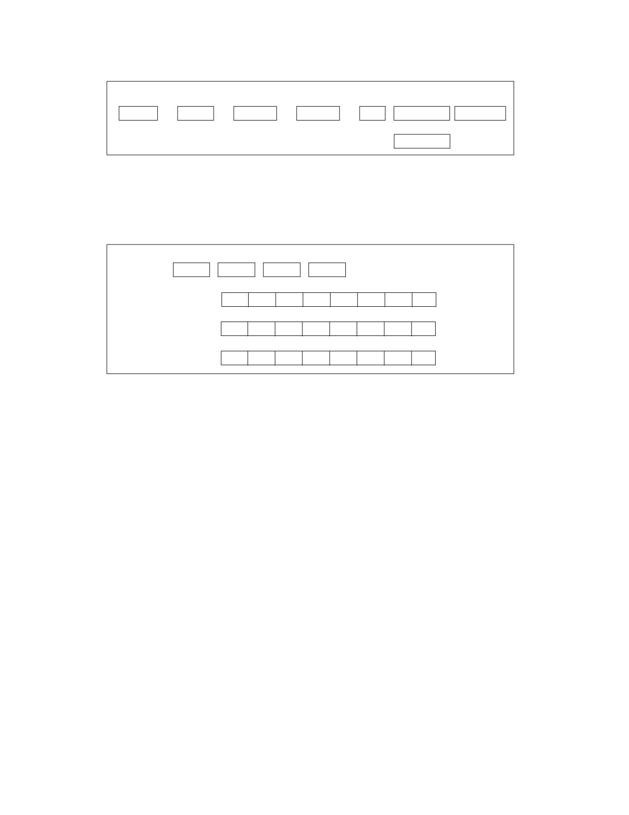
INSTRUCTION FORMAT
# of bytes:
4
1
1
1
2, 4
1
[Prefixes]
EVEX
Opcode
ModR/M
[SIB]
[Disp16,32]
[Immediate]
1
[Disp8*N]
Figure 2-10. Intel® AVX-512 Instruction Format and the EVEX Prefix
The EVEX prefix is a 4-byte prefix, with the first two bytes derived from unused encoding form of the 32-bit-mode-
only BOUND instruction. The layout of the EVEX prefix is shown in Figure 2-11. The first byte must be 62H, followed
by three payload bytes, denoted as P0, P1, and P2 individually or collectively as P[23:0] (see Figure 2-11).
EVEX
62H
P0
P1
P2
7
6
5
4
3
2
1
0
R
X
B
R’
0
m
m
m
P[7:0]
P0
7
6
5
4
3
2
1
0
P1
W
v
v
v
v
1
p
p
P[15:8]
7
6
5
4
3
2
1
0
P2
z
L’
L
b
V’
a
a
a
P[23:16]
Figure 2-11. Bit Field Layout of the EVEX Prefix1
NOTES:
1. See Table 2-32 for additional details on bit fields.
Vol. 2A
2-37

INSTRUCTION FORMAT
Table 2-32. EVEX Prefix Bit Field Functional Grouping
Notation
Bit field Group
Position
Comment
EVEX.mmm
Access to up to eight decoding maps
P[2:0]
Currently, only the following decoding maps are supported: 1,
2, 3, 5, and 6.
--
Reserved
P[3]
Must be 0.
EVEX.R’
High-16 register specifier modifier
P[4]
Combine with EVEX.R and ModR/M.reg. This bit is stored in
inverted format.
EVEX.RXB
Next-8 register specifier modifier
P[7:5]
Combine with ModR/M.reg, ModR/M.rm (base, index/vidx). This
field is encoded in bit inverted format.
EVEX.X
High-16 register specifier modifier
P[6]
Combine with EVEX.B and ModR/M.rm, when SIB/VSIB absent.
EVEX.pp
Compressed legacy prefix
P[9:8]
Identical to VEX.pp.
--
Fixed Value
P[10]
Must be 1.
EVEX.vvvv
VVVV register specifier
P[14:11]
Same as VEX.vvvv. This field is encoded in bit inverted format.
EVEX.W
Operand size promotion/Opcode
P[15]
extension
EVEX.aaa
Embedded opmask register specifier
P[18:16]
EVEX.V’
High-16 VVVV/VIDX register specifier
P[19]
Combine with EVEX.vvvv or when VSIB present. This bit is
stored in inverted format.
EVEX.b
Broadcast/RC/SAE Context
P[20]
EVEX.L’L
Vector length/RC
P[22:21]
EVEX.z
Zeroing/Merging
P[23]
The bit fields in P[23:0] are divided into the following functional groups (Table 2-32 provides a tabular summary):
• Reserved bits: P[3] must be 0, otherwise #UD.
• Fixed-value bit: P[10] must be 1, otherwise #UD.
• Compressed legacy prefix/escape bytes: P[1:0] is identical to the lowest 2 bits of VEX.mmmmm; P[9:8] is
identical to VEX.pp.
• EVEX.mmm: P[2:0] provides access to up to eight decoding maps. Currently, only the following decoding maps
are supported: 1, 2, 3, 5, and 6. Map ids 1, 2, and 3 are denoted by 0F, 0F38, and 0F3A, respectively, in the
instruction encoding descriptions.
• Operand specifier modifier bits for vector register, general purpose register, memory addressing: P[7:5] allows
access to the next set of 8 registers beyond the low 8 registers when combined with ModR/M register specifiers.
• Operand specifier modifier bit for vector register: P[4] (or EVEX.R’) allows access to the high 16 vector register
set when combined with P[7] and ModR/M.reg specifier; P[6] can also provide access to a high 16 vector
register when SIB or VSIB addressing are not needed.
• Non-destructive source /vector index operand specifier: P[19] and P[14:11] encode the second source vector
register operand in a non-destructive source syntax, vector index register operand can access an upper 16
vector register using P[19].
• Op-mask register specifiers: P[18:16] encodes op-mask register set k0-k7 in instructions operating on vector
registers.
• EVEX.W: P[15] is similar to VEX.W which serves either as opcode extension bit or operand size promotion to
64-bit in 64-bit mode.
• Vector destination merging/zeroing: P[23] encodes the destination result behavior which either zeroes the
masked elements or leave masked element unchanged.
• Broadcast/Static-rounding/SAE context bit: P[20] encodes multiple functionality, which differs across different
classes of instructions and can affect the meaning of the remaining field (EVEX.L’L). The functionality for the
following instruction classes are:
2-38
Vol. 2A
INSTRUCTION FORMAT
- Broadcasting a single element across the destination vector register: this applies to the instruction class
with Load+Op semantic where one of the source operand is from memory.
- Redirect L’L field (P[22:21]) as static rounding control for floating-point instructions with rounding
semantic. Static rounding control overrides MXCSR.RC field and implies “Suppress all exceptions” (SAE).
- Enable SAE for floating -point instructions with arithmetic semantic that is not rounding.
- For instruction classes outside of the afore-mentioned three classes, setting EVEX.b will cause #UD.
• Vector length/rounding control specifier: P[22:21] can serve one of three options.
- Vector length information for packed vector instructions.
- Ignored for instructions operating on vector register content as a single data element.
- Rounding control for floating-point instructions that have a rounding semantic and whose source and
destination operands are all vector registers.
2.7.2
Register Specifier Encoding and EVEX
EVEX-encoded instruction can access 8 opmask registers, 16 general-purpose registers and 32 vector registers in
64-bit mode (8 general-purpose registers and 8 vector registers in non-64-bit modes). EVEX-encoding can support
instruction syntax that access up to 4 instruction operands. Normal memory addressing modes and VSIB memory
addressing are supported with EVEX prefix encoding. The mapping of register operands used by various instruction
syntax and memory addressing in 64-bit mode are shown in Table 2-33. Opmask register encoding is described in
Section 2.7.3.
Table 2-33. 32-Register Support in 64-bit Mode Using EVEX with Embedded REX Bits
41
3
[2:0]
Reg. Type
Common Usages
REG
EVEX.R’
REX.R
modrm.reg
GPR, Vector
Destination or Source
VVVV
EVEX.V’
EVEX.vvvv
GPR, Vector
2ndSource or Destination
RM
EVEX.X
EVEX.B
modrm.r/m
GPR, Vector
1st Source or Destination
BASE
0
EVEX.B
modrm.r/m
GPR
memory addressing
INDEX
0
EVEX.X
sib.index
GPR
memory addressing
VIDX
EVEX.V’
EVEX.X
sib.index
Vector
VSIB memory addressing
NOTES:
1. Not applicable for accessing general purpose registers.
The mapping of register operands used by various instruction syntax and memory addressing in 32-bit modes are
shown in Table 2-34.
Table 2-34. EVEX Encoding Register Specifiers in 32-bit Mode
[2:0]
Reg. Type
Common Usages
REG
modrm.reg
GPR, Vector
Destination or Source
VVVV
EVEX.vvv
GPR, Vector
2nd Source or Destination
RM
modrm.r/m
GPR, Vector
1st Source or Destination
BASE
modrm.r/m
GPR
Memory Addressing
INDEX
sib.index
GPR
Memory Addressing
VIDX
sib.index
Vector
VSIB Memory Addressing
Vol. 2A
2-39

INSTRUCTION FORMAT
2.7.3
Opmask Register Encoding
There are eight opmask registers, k0-k7. Opmask register encoding falls into two categories:
• Opmask registers that are the source or destination operands of an instruction treating the content of opmask
register as a scalar value, are encoded using the VEX prefix scheme. It can support up to three operands using
standard modR/M byte’s reg field and rm field and VEX.vvvv. Such a scalar opmask instruction does not support
conditional update of the destination operand.
• An opmask register providing conditional processing and/or conditional update of the destination register of a
vector instruction is encoded using EVEX.aaa field (see Section 2.7.4).
• An opmask register serving as the destination or source operand of a vector instruction is encoded using
standard modR/M byte’s reg field and rm fields.
Table 2-35. Opmask Register Specifier Encoding
[2:0]
Register Access
Common Usages
REG
modrm.reg
k0-k7
Source
VVVV
VEX.vvvv
k0-k7
2nd Source
RM
modrm.r/m
k0-7
1st Source
{k1}
EVEX.aaa
k01-k7
Opmask
NOTES:
1. Instructions that overwrite the conditional mask in opmask do not permit using k0 as the embedded mask.
2.7.4
Masking Support in EVEX
EVEX can encode an opmask register to conditionally control per-element computational operation and updating of
result of an instruction to the destination operand. The predicate operand is known as the opmask register. The
EVEX.aaa field, P[18:16] of the EVEX prefix, is used to encode one out of a set of eight 64-bit architectural regis-
ters. Note that from this set of 8 architectural registers, only k1 through k7 can be addressed as predicate oper-
ands. k0 can be used as a regular source or destination but cannot be encoded as a predicate operand.
AVX-512 instructions support two types of masking with EVEX.z bit (P[23]) controlling the type of masking:
• Merging-masking, which is the default type of masking for EVEX-encoded vector instructions, preserves the old
value of each element of the destination where the corresponding mask bit has a 0. It corresponds to the case
of EVEX.z = 0.
• Zeroing-masking, is enabled by having the EVEX.z bit set to 1. In this case, an element of the destination is set
to 0 when the corresponding mask bit has a 0 value.
AVX-512 Foundation instructions can be divided into the following groups:
• Instructions which support “zeroing-masking”.
- Also allow merging-masking.
• Instructions which require aaa = 000.
- Do not allow any form of masking.
• Instructions which allow merging-masking but do not allow zeroing-masking.
- Require EVEX.z to be set to 0.
- This group is mostly composed of instructions that write to memory.
• Instructions which require aaa <> 000 do not allow EVEX.z to be set to 1.
— Allow merging-masking and do not allow zeroing-masking, e.g., gather instructions.
2-40
Vol. 2A
INSTRUCTION FORMAT
2.7.5
Compressed Displacement (disp8*N) Support in EVEX
For memory addressing using disp8 form, EVEX-encoded instructions always use a compressed displacement
scheme by multiplying disp8 in conjunction with a scaling factor N that is determined based on the vector length,
the value of EVEX.b bit (embedded broadcast) and the input element size of the instruction. In general, the factor
N corresponds to the number of bytes characterizing the internal memory operation of the input operand (e.g., 64
when the accessing a full 512-bit memory vector). The scale factor N is listed in Table 2-36 and Table 2-37 below,
where EVEX encoded instructions are classified using the tupletype attribute. The scale factor N of each tupletype
is listed based on the vector length (VL) and other factors affecting it.
Table 2-36 covers EVEX-encoded instructions which has a load semantic in conjunction with additional computa-
tional or data element movement operation, operating either on the full vector or half vector (due to conversion of
numerical precision from a wider format to narrower format). EVEX.b is supported for such instructions for data
element sizes which are either dword or qword (see Section 2.7.11).
EVEX-encoded instruction that are pure load/store, and “Load+op” instruction semantic that operate on data
element size less then dword do not support broadcasting using EVEX.b. These are listed in Table 2-37. Table 2-37
also includes many broadcast instructions which perform broadcast using a subset of data elements without using
EVEX.b. These instructions and a few data element size conversion instruction are covered in Table 2-37. Instruc-
tion classified in Table 2-37 do not use EVEX.b and EVEX.b must be 0, otherwise #UD will occur.
The tupletype will be referenced in the instruction operand encoding table in the reference page of each instruction,
providing the cross reference for the scaling factor N to encoding memory addressing operand.
Note that the disp8*N rules still apply when using 16b addressing.
Table 2-36. Compressed Displacement (DISP8*N) Affected by Embedded Broadcast
TupleType
EVEX.b
InputSize
EVEX.W
Broadcast
N (VL=128)
N (VL=256)
N (VL= 512)
Comment
0
32bit
0
none
16
32
64
1
32bit
0
{1tox}
4
4
4
Load+Op (Full Vector
Full
0
64bit
1
none
16
32
64
Dword/Qword)
1
64bit
1
{1tox}
8
8
8
0
32bit
0
none
8
16
32
Half
Load+Op (Half Vector)
1
32bit
0
{1tox}
4
4
4
Table 2-37. EVEX DISP8*N for Instructions Not Affected by Embedded Broadcast
TupleType
InputSize
EVEX.W
N (VL= 128)
N (VL= 256)
N (VL= 512)
Comment
Full Mem
N/A
N/A
16
32
64
Load/store or subDword full vector
8bit
N/A
1
1
1
16bit
N/A
2
2
2
Tuple1 Scalar
1Tuple
32bit
0
4
4
4
64bit
1
8
8
8
32bit
N/A
4
4
4
1 Tuple, memsize not affected by
Tuple1 Fixed
64bit
N/A
8
8
8
EVEX.W
32bit
0
8
8
8
Tuple2
Broadcast (2 elements)
64bit
1
NA
16
16
32bit
0
NA
16
16
Tuple4
Broadcast (4 elements)
64bit
1
NA
NA
32
Tuple8
32bit
0
NA
NA
32
Broadcast (8 elements)
Half Mem
N/A
N/A
8
16
32
SubQword Conversion
Quarter Mem
N/A
N/A
4
8
16
SubDword Conversion
Vol. 2A
2-41

INSTRUCTION FORMAT
Table 2-37. EVEX DISP8*N for Instructions Not Affected by Embedded Broadcast (Contd.)
TupleType
InputSize
EVEX.W
N (VL= 128)
N (VL= 256)
N (VL= 512)
Comment
Eighth Mem
N/A
N/A
2
4
8
SubWord Conversion
Mem128
N/A
N/A
16
16
16
Shift count from memory
MOVDDUP
N/A
N/A
8
32
64
VMOVDDUP
2.7.6
EVEX Encoding of Broadcast/Rounding/SAE Support
EVEX.b can provide three types of encoding context, depending on the instruction classes:
• Embedded broadcasting of one data element from a source memory operand to the destination for vector
instructions with “load+op” semantic.
• Static rounding control overriding MXCSR.RC for floating-point instructions with rounding semantic.
• “Suppress All exceptions” (SAE) overriding MXCSR mask control for floating-point arithmetic instructions that
do not have rounding semantic.
2.7.7
Embedded Broadcast Support in EVEX
EVEX encodes an embedded broadcast functionality that is supported on many vector instructions with 32-bit
(double word or single precision floating-point) and 64-bit data elements, and when the source operand is from
memory. EVEX.b (P[20]) bit is used to enable broadcast on load-op instructions. When enabled, only one element
is loaded from memory and broadcasted to all other elements instead of loading the full memory size.
The following instruction classes do not support embedded broadcasting:
• Instructions with only one scalar result is written to the vector destination.
• Instructions with explicit broadcast functionality provided by its opcode.
• Instruction semantic is a pure load or a pure store operation.
2.7.8
Static Rounding Support in EVEX
Static rounding control embedded in the EVEX encoding system applies only to register-to-register flavor of
floating-point instructions with rounding semantic at two distinct vector lengths: (i) scalar, (ii) 512-bit. In both
cases, the field EVEX.L’L expresses rounding mode control overriding MXCSR.RC if EVEX.b is set. When EVEX.b is
set, “suppress all exceptions” is implied. The processor behaves as if all MXCSR masking controls are set.
2.7.9
SAE Support in EVEX
The EVEX encoding system allows arithmetic floating-point instructions without rounding semantic to be encoded
with the SAE attribute. This capability applies to scalar and 512-bit vector lengths, register-to-register only, by
setting EVEX.b. When EVEX.b is set, “suppress all exceptions” is implied. The processor behaves as if all MXCSR
masking controls are set.
2.7.10 Vector Length Orthogonality
The architecture of EVEX encoding scheme can support SIMD instructions operating at multiple vector lengths.
Many AVX-512 Foundation instructions operate at 512-bit vector length. The vector length of EVEX encoded vector
instructions are generally determined using the L’L field in EVEX prefix, except for 512-bit floating-point, reg-reg
instructions with rounding semantic. The table below shows the vector length corresponding to various values of
the L’L bits. When EVEX is used to encode scalar instructions, L’L is generally ignored.
When EVEX.b bit is set for a register-register instructions with floating-point rounding semantic, the same two bits
P2[6:5] specifies rounding mode for the instruction, with implied SAE behavior. The mapping of different instruc-
tion classes relative to the embedded broadcast/rounding/SAE control and the EVEX.L’L fields are summarized in
Table 2-38.
2-42
Vol. 2A
INSTRUCTION FORMAT
Table 2-38. EVEX Embedded Broadcast/Rounding/SAE and Vector Length on Vector Instructions
Position
P2[4]
P2[6:5]
P2[6:5]
Broadcast/Rounding/SAE Context
EVEX.b
EVEX.L’L
EVEX.RC
Reg-reg, FP Instructions w/ rounding semantic or SAE
Enable static rounding
Vector length Implied
00b: SAE + RNE
control (SAE implied)
(512 bit or scalar)
01b: SAE + RD
10b: SAE + RU
11b: SAE + RZ
Load+op Instructions w/ memory source
Broadcast Control
00b: 128-bit
NA
01b: 256-bit
Other Instructions (
Must be 0 (otherwise
NA
10b: 512-bit
Explicit Load/Store/Broadcast/Gather/Scatter)
#UD)
11b: Reserved (#UD)
2.7.11 #UD Equations for EVEX
Instructions encoded using EVEX can face three types of UD conditions: state dependent, opcode independent and
opcode dependent.
2.7.11.1 State Dependent #UD
In general, attempts of execute an instruction, which required OS support for incremental extended state compo-
nent, will #UD if required state components were not enabled by OS. Table 2-39 lists instruction categories with
respect to required processor state components. Attempts to execute a given category of instructions while
enabled states were less than the required bit vector in XCR0 shown in Table 2-39 will cause #UD.
Table 2-39. OS XSAVE Enabling Requirements of Instruction Categories
Instruction Categories
Vector Register State Access
Required XCR0 Bit Vector [7:0]
Legacy SIMD prefix encoded Instructions (e.g SSE)
XMM
xxxxxx11b
VEX-encoded instructions operating on YMM
YMM
xxxxx111b
EVEX-encoded 128-bit instructions
ZMM
111xx111b
EVEX-encoded 256-bit instructions
ZMM
111xx111b
EVEX-encoded 512-bit instructions
ZMM
111xx111b
VEX-encoded instructions operating on opmask
k-reg
111xxx11b
2.7.11.2 Opcode Independent #UD
A number of bit fields in EVEX encoded instruction must obey mode-specific but opcode-independent patterns
listed in Table 2-40.
Table 2-40. Opcode Independent, State Dependent EVEX Bit Fields1
Position
Notation
64-bit #UD
Non-64-bit #UD
P[3]
--
if > 0
if > 0
P[10]
--
if 0
if 0
P[2:0]
EVEX.mmm
if 000b, 100b, or 111b
if 000b, 100b, or 111b
P[7 : 6]
EVEX.RX
None (valid)
None (BOUND if EVEX.RX != 11b)
NOTES:
1. This table is also representative of VEX restrictions. For VEX operations, use the Notation field.
Vol. 2A
2-43
INSTRUCTION FORMAT
2.7.11.3 Opcode Dependent #UD
This section describes legal values for the rest of the EVEX bit fields. Table 2-41 lists the #UD conditions of EVEX
prefix bit fields which encodes or modifies register operands.
Table 2-41. #UD Conditions of Operand-Encoding EVEX Prefix Bit Fields1
Notation
Position
Operand Encoding
64-bit #UD
Non-64-bit #UD
EVEX.R
P[7]
ModRM.reg encodes k-reg
If EVEX.R = 0
None (BOUND if
EVEX.RX != 11b)
ModRM.reg is opcode extension
None (ignored)
ModRM.reg encodes all other registers
None (valid)
EVEX.X
P[6]
ModRM.r/m encodes ZMM/YMM/XMM
None (valid)
ModRM.r/m encodes k-reg or GPR
None (ignored)
ModRM.r/m without SIB/VSIB
None (ignored)
ModRM.r/m with SIB/VSIB
None (valid)
EVEX.B
P[5]
ModRM.r/m encodes k-reg
None (ignored)
None (ignored)
ModRM.r/m encodes other registers
None (valid)
ModRM.r/m base present
None (valid)
ModRM.r/m base not present
None (ignored)
EVEX.R’
P[4]
ModRM.reg encodes k-reg or GPR
If 0
None (ignored)
ModRM.reg is opcode extension
None (ignored)
ModRM.reg encodes ZMM/YMM/XMM
None (valid)
EVEX.vvvv
P[14:11]
vvvv encodes ZMM/YMM/XMM
None (valid)
None (valid)
P[14] ignored
Otherwise
If != 1111b
If != 1111b
EVEX.V’
P[19]
Encodes ZMM/YMM/XMM
None (valid)
If 0
Otherwise
If 0
If 0
NOTES:
1. This table also represents VEX restrictions.
Table 2-42 lists the #UD conditions of instruction encoding of opmask register using EVEX.aaa and EVEX.z
Table 2-42. #UD Conditions of Opmask Related Encoding Field
Notation
Position
Operand Encoding
64-bit #UD
Non-64-bit #UD
EVEX.aaa
P[18:16]
Instructions do not use opmask for conditional processing1.
If aaa != 000b
If aaa != 000b
Opmask used as conditional processing mask and updated
If aaa = 000b
If aaa = 000b;
at completion2.
Opmask used as conditional processing.
None (valid3)
None (valid1)
EVEX.z
P[23]
Vector instruction using opmask as source or destination4.
If EVEX.z != 0
If EVEX.z != 0
Store instructions or gather/scatter instructions.
If EVEX.z != 0
If EVEX.z != 0
Instructions with EVEX.aaa = 000b.
If EVEX.z != 0
If EVEX.z != 0
VEX.vvvv
Varies
K-regs are instruction operands not mask control.
If vvvv = 0xxxb
None
NOTES:
1. E.g., VPBROADCASTMxxx, VPMOVM2x, VPMOVx2M.
2. E.g., Gather/Scatter family.
2-44
Vol. 2A
INSTRUCTION FORMAT
3. aaa can take any value. A value of 000 indicates that there is no masking on the instruction; in this case, all elements will be pro-
cessed as if there was a mask of ‘all ones’ regardless of the actual value in K0.
4. E.g., VFPCLASSPD/PS, VCMPB/D/Q/W family, VPMOVM2x, VPMOVx2M.
Table 2-43 lists the #UD conditions of EVEX bit fields that depends on the context of EVEX.b.
Table 2-43. #UD Conditions Dependent on EVEX.b Context
Notation
Position
Operand Encoding
64-bit #UD
Non-64-bit #UD
EVEX.L’Lb
P[22 : 20]
Reg-reg, FP instructions with rounding semantic.
None (valid1)
None (valid1)
Other reg-reg, FP instructions that can cause #XM.
None (valid2)
None (valid2)
Other reg-mem instructions in Table 2-36.
None (valid3)
None (valid3)
Other instruction classes4 in Table 2-37.
If EVEX.b = 1
If EVEX.b = 1
NOTES:
1. L’L specifies rounding control, see Table 2-38, supports {er} syntax.
2. L’L is ignored.
3. L’L specifies vector length, see Table 2-38, supports embedded broadcast syntax
4. L’L specifies either vector length or ignored.
2.7.12 Device Not Available
EVEX-encoded instructions follow the same rules when it comes to generating #NM (Device Not Available) excep-
tion. In particular, it is generated when CR0.TS[bit 3]= 1.
2.7.13 Scalar Instructions
EVEX-encoded scalar SIMD instructions can access up to 32 registers in 64-bit mode. Scalar instructions support
masking (using the least significant bit of the opmask register), but broadcasting is not supported.
2.8
EXCEPTION CLASSIFICATIONS OF EVEX-ENCODED INSTRUCTIONS
The exception behavior of EVEX-encoded instructions can be classified into the classes shown in the rest of this
section. The classification of EVEX-encoded instructions follow a similar framework as those of AVX and AVX2
instructions using the VEX prefix. Exception types for EVEX-encoded instructions are named in the style of
“E##” or with a suffix “E##XX”. The “##” designation generally follows that of AVX/AVX2 instructions. The
majority of EVEX encoded instruction with “Load+op” semantic supports memory fault suppression, which is repre-
sented by E##. The instructions with “Load+op” semantic but do not support fault suppression are named
“E##NF”. A summary table of exception classes by class names are shown below.
Vol. 2A
2-45

INSTRUCTION FORMAT
Table 2-44. EVEX-Encoded Instruction Exception Class Summary
Exception Class
Instruction set
Mem arg
(#XM)
Type E1
Vector Moves/Load/Stores
Explicitly aligned, w/ fault suppression
None
Type E1NF
Vector Non-temporal Stores
Explicitly aligned, no fault suppression
None
Type E2
FP Vector Load+op
Support fault suppression
Yes
Type E2NF
FP Vector Load+op
No fault suppression
Yes
Type E3
FP Scalar/Partial Vector, Load+Op
Support fault suppression
Yes
Type E3NF
FP Scalar/Partial Vector, Load+Op
No fault suppression
Yes
Type E4
Integer Vector Load+op
Support fault suppression
No
Type E4NF
Integer Vector Load+op
No fault suppression
No
Type E5
Legacy-like Promotion
Varies, Support fault suppression
No
Type E5NF
Legacy-like Promotion
Varies, No fault suppression
No
Type E6
Post AVX Promotion
Varies, w/ fault suppression
No
Type E6NF
Post AVX Promotion
Varies, no fault suppression
No
Type E7NM
Register-to-register op
None
None
Type E9NF
Miscellaneous 128-bit
Vector-length Specific, no fault suppression
None
Type E10
Non-XF Scalar
Vector Length ignored, w/ fault suppression
None
Type E10NF
Non-XF Scalar
Vector Length ignored, no fault suppression
None
Type E11
VCVTPH2PS, VCVTPS2PH
Half Vector Length, w/ fault suppression
Yes
Type E12
Gather and Scatter Family
VSIB addressing, w/ fault suppression
None
Type E12NP
Gather and Scatter Prefetch Family
VSIB addressing, w/o page fault
None
Table 2-45 lists EVEX-encoded instruction mnemonic by exception classes.
Table 2-45. EVEX Instructions in Each Exception Class
Exception Class
Instruction
Type E1
VMOVAPD, VMOVAPS, VMOVDQA32, VMOVDQA64
Type E1NF
VMOVNTDQ, VMOVNTDQA, VMOVNTPD, VMOVNTPS
VADDPD, VADDPH, VADDPS, VCMPPD, VCMPPH, VCMPPS, VCVTDQ2PH, VCVTDQ2PS, VCVTPD2DQ, VCVTPD2PH,
VCVTPD2PS, VCVTPD2QQ, VCVTPD2UQQ, VCVTPD2UDQ, VCVTPH2DQ, VCVTPH2PD, VCVTPH2QQ, VCVTPH2UDQ,
VCVTPH2UQQ, VCVTPH2UW, VCVTPH2W, VCVTPS2DQ, VCVTPS2PD, VCVTPS2QQ, VCVTPS2UDQS, VCVTPS2UQQ,
VCVTQQ2PD, VCVTQQ2PH, VCVTQQ2PS, VCVTTPD2DQ, VCVTTPD2QQ, VCVTTPD2UDQ, VCVTTPD2UQQ,
VCVTTPH2DQ, VCVTTPH2QQ, VCVTTPH2UDQ, VCVTTPH2UQQ, VCVTTPH2UW, VCVTTPH2W, VCVTTPS2DQ,
VCVTTPS2QQ, VCVTTPS2UDQ, VCVTTPS2UQQ, VCVTUDQ2PH, VCVTUDQ2PS, VCVTUQQ2PD, VCVTUQQ2PH,
VCVTUQQ2PS, VCVTUW2PH, VCVTW2PH, VDIVPD, VDIVPH, VDIVPS, VEXP2PD, VEXP2PS, VFIXUPIMMPD,
Type E2
VFIXUPIMMPS, VFMADDxxxPD, VFMADDxxxPH, VFMADDxxxPS, VFMADDSUBxxxPD, VFMADDSUBxxxPH,
VFMADDSUBxxxPS, VFMSUBADDxxxPD, VFMSUBADDxxxPH, VFMSUBADDxxxPS, VFMSUBxxxPD, VFMSUBxxxPH,
VFMSUBxxxPS, VFNMADDxxxPD, VFNMADDxxxPH, VFNMADDxxxPS, VFNMSUBxxxPD, VFNMSUBxxxPH,
VFNMSUBxxxPS, VGETEXPPD, VGETEXPPH, VGETEXPPS, VGETMANTPD, VGETMANTPH, VGETMANTPS,
VGETMANTSH, VMAXPD, VMAXPH, VMAXPS, VMINPD, VMINPH, VMINPS, VMULPD, VMULPH, VMULPS, VRANGEPD,
VRANGEPS, VREDUCEPD, VREDUCEPH, VREDUCEPS, VRNDSCALEPD, VRNDSCALEPH, VRNDSCALEPS, VRCP28PD,
VRCP28PS, VRSQRT28PD, VRSQRT28PS, VSCALEFPD, VSCALEFPS, VSQRTPD, VSQRTPH, VSQRTPS, VSUBPD,
VSUBPH, VSUBPS
2-46
Vol. 2A

INSTRUCTION FORMAT
Table 2-45. EVEX Instructions in Each Exception Class (Contd.)
Exception Class
Instruction
VADDSD, VADDSH, VADDSS, VCMPSD, VCMPSH, VCMPSS, VCVTSD2SH, VCVTSD2SS, VCVTSH2SD, VCVTSH2SS,
VCVTSS2SD, VCVTSS2SH, VDIVSD, VDIVSH, VDIVSS, VFMADDxxxSD, VFMADDxxxSH, VFMADDxxxSS,
VFMSUBxxxSD, VFMSUBxxxSH, VFMSUBxxxSS, VFNMADDxxxSD, VFNMADDxxxSH, VFNMADDxxxSS,
VFNMSUBxxxSD, VFNMSUBxxxSH, VFNMSUBxxxSS, VFIXUPIMMSD, VFIXUPIMMSS, VGETEXPSD, VGETEXPSH,
Type E3
VGETEXPSS, VGETMANTSD, VGETMANTSH, VGETMANTSS, VMAXSD, VMAXSH, VMAXSS, VMINSD, VMINSH, VMINSS,
VMULSD, VMULSH, VMULSS, VRANGESD, VRANGESS, VREDUCESD, VREDUCESH, VREDUCESS, VRNDSCALESD,
VRNDSCALESH, VRNDSCALESS, VSCALEFSD, VSCALEFSH, VSCALEFSS, VRCP28SD, VRCP28SS, VRSQRT28SD,
VRSQRT28SS, VSQRTSD, VSQRTSH, VSQRTSS, VSUBSD, VSUBSH, VSUBSS
VCOMISD, VCOMISH, VCOMISS, VCVTSD2SI, VCVTSD2USI, VCVTSH2SI, VCVTSH2USI, VCVTSI2SD, VCVTSI2SH,
Type E3NF
VCVTSI2SS, VCVTSS2SI, VCVTSS2USI, VCVTTSD2SI, VCVTTSD2USI, VCVTTSH2SI, VCVTTSH2USI, VCVTTSS2SI,
VCVTTSS2USI, VCVTUSI2SD, VCVTUSI2SH, VCVTUSI2SS, VUCOMISD, VUCOMISH, VUCOMISS
VANDPD, VANDPS, VANDNPD, VANDNPS, VBLENDMPD, VBLENDMPS, VFCMADDCPH, VFCMULCPH, VFMADDCPH,
VFMULCPH, VFPCLASSPD, VFPCLASSPH, VFPCLASSPS, VORPD, VORPS, VPABSD, VPABSQ, VPADDD, VPADDQ,
VPANDD, VPANDQ, VPANDND, VPANDNQ, VPBLENDMB, VPBLENDMD, VPBLENDMQ, VPBLENDMW, VPCMPD,
VPCMPEQD, VPCMPEQQ, VPCMPGTD, VPCMPGTQ, VPCMPQ, VPCMPUD, VPCMPUQ, VPLZCNTD, VPLZCNTQ,
VPMADD52LUQ, VPMADD52HUQ, VPMAXSD, VPMAXSQ, VPMAXUD, VPMAXUQ, VPMINSD, VPMINSQ, VPMINUD,
Type E4
VPMINUQ, VPMULLD, VPMULLQ, VPMULUDQ, VPMULDQ, VPORD, VPORQ, VPROLD, VPROLQ, VPROLVD, VPROLVQ,
VPRORD, VPRORQ, VPRORVD, VPRORVQ, VPSHUFBITQMB, VPSLLD, VPSLLQ, VPSRAD, VPSRAQ, VPSRAVW,
VPSRAVD, VPSRAVW, VPSRAVQ, VPSRLD, VPSRLQ)1, VPSUBD, VPSUBQ, VPSUBUSB, VPSUBUSW, VPTERNLOGD,
VPTERNLOGQ, VPTESTMD, VPTESTMQ, VPTESTNMD, VPTESTNMQ, VPXORD, VPXORQ, VPSLLVD, VPSLLVQ,
VRCP14PD, VRCP14PS, VRCPPH, VRSQRT14PD, VRSQRT14PS, VRSQRTPH, VXORPD, VXORPS
VCOMPRESSPD, VCOMPRESSPS, VEXPANDPD, VEXPANDPS, VMOVDQU8, VMOVDQU16, VMOVDQU32,
VMOVDQU64, VMOVUPD, VMOVUPS, VPABSB, VPABSW, VPADDB, VPADDW, VPADDSB, VPADDSW, VPADDUSB,
VPADDUSW, VPAVGB, VPAVGW, VPCMPB, VPCMPEQB, VPCMPEQW, VPCMPGTB, VPCMPGTW, VPCMPW, VPCMPUB,
E4.nb2
VPCMPUW, VPCOMPRESSD, VPCOMPRESSQ, VPEXPANDD, VPEXPANDQ, VPMAXSB, VPMAXSW, VPMAXUB,
VPMAXUW, VPMINSB, VPMINSW, VPMINUB, VPMINUW, VPMULHRSW, VPMULHUW, VPMULHW, VPMULLW,
VPSLLVW, VPSLLW, VPSRAW, VPSRLVW, VPSRLW, VPSUBB, VPSUBW, VPSUBSB, VPSUBSW, VPTESTMB,
VPTESTMW, VPTESTNMB, VPTESTNMW
VALIGND, VALIGNQ, VPACKSSDW, VPACKUSDW, VPCONFLICTD, VPCONFLICTQ, VPERMD, VPERMI2D, VPERMI2PS,
VPERMI2PD, VPERMI2Q, VPERMPD, VPERMPS, VPERMQ, VPERMT2D, VPERMT2PS, VPERMT2Q, VPERMT2PD,
Type E4NF
VPERMILPD, VPERMILPS, VPMULTISHIFTQB, VPSHUFD, VPUNPCKHDQ, VPUNPCKHQDQ, VPUNPCKLDQ,
VPUNPCKLQDQ, VSHUFF32X4, VSHUFF64X2, VSHUFI32X4, VSHUFI64X2, VSHUFPD, VSHUFPS, VUNPCKHPD,
VUNPCKHPS, VUNPCKLPD, VUNPCKLPS
VDBPSADBW, VPACKSSWB, VPACKUSWB, VPALIGNR, VPMADDWD, VPMADDUBSW, VMOVSHDUP, VMOVSLDUP,
VPSADBW, VPSHUFB, VPSHUFHW, VPSHUFLW, VPSLLDQ, VPSRLDQ, VPSLLW, VPSRAW, VPSRLW, (VPSLLD,
E4NF.nb2
VPSLLQ, VPSRAD, VPSRAQ, VPSRLD, VPSRLQ)3, VPUNPCKHBW, VPUNPCKHWD, VPUNPCKLBW, VPUNPCKLWD,
VPERMW, VPERMI2W, VPERMT2W
PMOVSXBW, PMOVSXBW, PMOVSXBD, PMOVSXBQ, PMOVSXWD, PMOVSXWQ, PMOVSXDQ, PMOVZXBW,
Type E5
PMOVZXBD, PMOVZXBQ, PMOVZXWD, PMOVZXWQ, PMOVZXDQ, VCVTDQ2PD, VCVTUDQ2PD, VMOVSH,
VPMOVSXxx, VPMOVZXxx,
Type E5NF
VMOVDDUP
VBROADCASTF32X2, VBROADCASTF32X4, VBROADCASTF64X2, VBROADCASTF32X8, VBROADCASTF64X4,
VBROADCASTI32X2, VBROADCASTI32X4, VBROADCASTI64X2, VBROADCASTI32X8, VBROADCASTI64X4,
VBROADCASTSD, VBROADCASTSS, VFPCLASSSD, VFPCLASSSS, VPBROADCASTB, VPBROADCASTD,
Type E6
VPBROADCASTW, VPBROADCASTQ, VPMOVQB, VPMOVSQB, VPMOVUSQB, VPMOVQW, VPMOVSQW, VPMOVUSQW,
VPMOVQD, VPMOVSQD, VPMOVUSQD, VPMOVDB, VPMOVSDB, VPMOVUSDB, VPMOVDW, VPMOVSDW,
VPMOVUSDW, VPMOVWB, VPMOVSWB, VPMOVUSWB
VEXTRACTF32X4, VEXTRACTF32X8, VEXTRACTF64X2, VEXTRACTF64X4, VEXTRACTI32X4, VEXTRACTI32X8,
Type E6NF
VEXTRACTI64X2, VEXTRACTI64X4, VINSERTF32X4, VINSERTF32X8, VINSERTF64X2, VINSERTF64X4,
VINSERTI32X4, VINSERTI32X8, VINSERTI64X2, VINSERTI64X4, VPBROADCASTMB2Q, VPBROADCASTMW2D
Vol. 2A
2-47

INSTRUCTION FORMAT
Table 2-45. EVEX Instructions in Each Exception Class (Contd.)
Exception Class
Instruction
Type
VMOVHLPS, VMOVLHPS
E7NM.1284
(VPBROADCASTD, VPBROADCASTQ, VPBROADCASTB, VPBROADCASTW)5, VPMOVB2M, VPMOVD2M, VPMOVM2B,
Type E7NM.
VPMOVM2D, VPMOVM2Q, VPMOVM2W, VPMOVQ2M, VPMOVW2M
VEXTRACTPS, VINSERTPS, VMOVHPD, VMOVHPS, VMOVLPD, VMOVLPS, VMOVD, VMOVQ, VMOVW, VPEXTRB,
Type E9NF
VPEXTRD, VPEXTRW, VPEXTRQ, VPINSRB, VPINSRD, VPINSRW, VPINSRQ
VFCMADDCSH, VFMADDCSH, VFCMULCSH, VFMULCSH, VFPCLASSSH, VMOVSD, VMOVSS, VRCP14SD, VRCP14SS,
Type E10
VRCPSH, VRSQRT14SD, VRSQRT14SS, VRSQRTSH
Type E10NF
(VCVTSI2SD, VCVTUSI2SD)6
Type E11
VCVTPH2PS, VCVTPS2PH
VGATHERDPS, VGATHERDPD, VGATHERQPS, VGATHERQPD, VPGATHERDD, VPGATHERDQ, VPGATHERQD,
Type E12
VPGATHERQQ, VPSCATTERDD, VPSCATTERDQ, VPSCATTERQD, VPSCATTERQQ, VSCATTERDPD, VSCATTERDPS,
VSCATTERQPD, VSCATTERQPS
VGATHERPF0DPD, VGATHERPF0DPS, VGATHERPF0QPD, VGATHERPF0QPS, VGATHERPF1DPD, VGATHERPF1DPS,
Type E12NP
VGATHERPF1QPD, VGATHERPF1QPS, VSCATTERPF0DPD, VSCATTERPF0DPS, VSCATTERPF0QPD,
VSCATTERPF0QPS, VSCATTERPF1DPD, VSCATTERPF1DPS, VSCATTERPF1QPD, VSCATTERPF1QPS
NOTES:
1. Operand encoding Full tupletype with immediate.
2. Embedded broadcast is not supported with the “.nb” suffix.
3. Operand encoding Mem128 tupletype.
4. #UD raised if EVEX.L’L !=00b (VL=128).
5. The source operand is a general purpose register.
6. W0 encoding only.
2.8.1
Exceptions Type E1 and E1NF of EVEX-Encoded Instructions
EVEX-encoded instructions with memory alignment restrictions, and supporting memory fault suppression follow
exception class E1.
2-48
Vol. 2A
INSTRUCTION FORMAT
Table 2-46. Type E1 Class Exception Conditions
Exception
Cause of Exception
X
X
If EVEX prefix present.
If CR4.OSXSAVE[bit 18]=0.
If any one of following conditions applies:
• State requirement, Table 2-39 not met.
• Opcode independent #UD condition in Table 2-40.
X
X
• Operand encoding #UD conditions in Table 2-41.
Invalid Opcode,
• Opmask encoding #UD condition of Table 2-42.
#UD
• EVEX.b encoding #UD condition of Table 2-43.
• Instruction specific EVEX.L'L restriction not met.
X
X
X
X
If preceded by a LOCK prefix (F0H).
X
X
If any REX, F2, F3, or 66 prefixes precede a EVEX prefix.
X
X
X
X
If any corresponding CPUID feature flag is ‘0’.
Device Not Avail-
X
X
X
X
If CR0.TS[bit 3]=1.
able, #NM
X
If fault suppression not set, and an illegal address in the SS segment.
Stack, #SS(0)
If fault suppression not set, and a memory address referencing the SS segment is in
X
a non-canonical form.
EVEX.512: Memory operand is not 64-byte aligned.
X
X
EVEX.256: Memory operand is not 32-byte aligned.
EVEX.128: Memory operand is not 16-byte aligned.
General Protection,
If fault suppression not set, and an illegal memory operand effective address in the
X
#GP(0)
CS, DS, ES, FS or GS segments.
X
If fault suppression not set, and the memory address is in a non-canonical form.
If fault suppression not set, and any part of the operand lies outside the effective
X
X
address space from 0 to FFFFH.
Page Fault
X
X
X
If fault suppression not set, and a page fault.
#PF(fault-code)
Vol. 2A
2-49
INSTRUCTION FORMAT
EVEX-encoded instructions with memory alignment restrictions, but do not support memory fault suppression
follow exception class E1NF.
Table 2-47. Type E1NF Class Exception Conditions
Exception
Cause of Exception
X
X
If EVEX prefix present.
If CR4.OSXSAVE[bit 18]=0.
If any one of following conditions applies:
• State requirement, Table 2-39 not met.
• Opcode independent #UD condition in Table 2-40.
X
X
• Operand encoding #UD conditions in Table 2-41.
Invalid Opcode,
• Opmask encoding #UD condition of Table 2-42.
#UD
• EVEX.b encoding #UD condition of Table 2-43.
• Instruction specific EVEX.L'L restriction not met.
X
X
X
X
If preceded by a LOCK prefix (F0H).
X
X
If any REX, F2, F3, or 66 prefixes precede a EVEX prefix.
X
X
X
X
If any corresponding CPUID feature flag is ‘0’.
Device Not Avail-
X
X
X
X
If CR0.TS[bit 3]=1.
able, #NM
X
For an illegal address in the SS segment.
Stack, #SS(0)
X
If a memory address referencing the SS segment is in a non-canonical form.
EVEX.512: Memory operand is not 64-byte aligned.
X
X
EVEX.256: Memory operand is not 32-byte aligned.
EVEX.128: Memory operand is not 16-byte aligned.
General Protection,
For an illegal memory operand effective address in the CS, DS, ES, FS or GS seg-
X
#GP(0)
ments.
X
If the memory address is in a non-canonical form.
X
X
If any part of the operand lies outside the effective address space from 0 to FFFFH.
Page Fault
X
X
X
For a page fault.
#PF(fault-code)
2.8.2
Exceptions Type E2 of EVEX-Encoded Instructions
EVEX-encoded vector instructions with arithmetic semantic follow exception class E2.
2-50
Vol. 2A
INSTRUCTION FORMAT
Table 2-48. Type E2 Class Exception Conditions
Exception
Cause of Exception
X
X
If EVEX prefix present.
X
X
X
X
If an unmasked SIMD floating-point exception and CR4.OSXMMEXCPT[bit 10] = 0.
If CR4.OSXSAVE[bit 18]=0.
If any one of following conditions applies:
• State requirement, Table 2-39 not met.
Invalid Opcode,
X
X
• Opcode independent #UD condition in Table 2-40.
#UD
• Operand encoding #UD conditions in Table 2-41.
• Opmask encoding #UD condition of Table 2-42.
• Instruction specific EVEX.L'L restriction not met.
X
X
X
X
If preceded by a LOCK prefix (F0H).
X
X
If any REX, F2, F3, or 66 prefixes precede a EVEX prefix.
X
X
X
X
If any corresponding CPUID feature flag is ‘0’.
Device Not Avail-
X
X
X
X
If CR0.TS[bit 3]=1.
able, #NM
X
If fault suppression not set, and an illegal address in the SS segment.
Stack, #SS(0)
If fault suppression not set, and a memory address referencing the SS segment is in a
X
non-canonical form.
If fault suppression not set, and an illegal memory operand effective address in the CS,
X
DS, ES, FS or GS segments.
General Protec-
X
If fault suppression not set, and the memory address is in a non-canonical form.
tion, #GP(0)
If fault suppression not set, and any part of the operand lies outside the effective
X
X
address space from 0 to FFFFH.
Page Fault
X
X
X
If fault suppression not set, and a page fault.
#PF(fault-code)
Alignment Check
For 2, 4, or 8 byte memory access if alignment checking is enabled and an unaligned
X
X
X
#AC(0)
memory access is made while the current privilege level is 3.
SIMD Floating-
If an unmasked SIMD floating-point exception, {sae} or {er} not set, and CR4.OSXMMEX-
point Exception,
X
X
X
X
CPT[bit 10] = 1.
#XM
2.8.3
Exceptions Type E3 and E3NF of EVEX-Encoded Instructions
EVEX-encoded scalar instructions with arithmetic semantic that support memory fault suppression follow exception
class E3.
Vol. 2A
2-51
INSTRUCTION FORMAT
Table 2-49. Type E3 Class Exception Conditions
Exception
Cause of Exception
X
X
If EVEX prefix present.
X
X
X
X
If an unmasked SIMD floating-point exception and CR4.OSXMMEXCPT[bit 10] = 0.
If CR4.OSXSAVE[bit 18]=0.
If any one of following conditions applies:
• State requirement, Table 2-39 not met.
X
X
• Opcode independent #UD condition in Table 2-40.
Invalid Opcode, #UD
• Operand encoding #UD conditions in Table 2-41.
• Opmask encoding #UD condition of Table 2-42.
• EVEX.b encoding #UD condition of Table 2-43.
X
X
X
X
If preceded by a LOCK prefix (F0H).
X
X
If any REX, F2, F3, or 66 prefixes precede a EVEX prefix.
X
X
X
X
If any corresponding CPUID feature flag is ‘0’.
Device Not Available,
X
X
X
X
If CR0.TS[bit 3]=1.
#NM
X
If fault suppression not set, and an illegal address in the SS segment.
Stack, #SS(0)
If fault suppression not set, and a memory address referencing the SS segment is
X
in a non-canonical form.
If fault suppression not set, and an illegal memory operand effective address in
X
the CS, DS, ES, FS or GS segments.
General Protection,
X
If fault suppression not set, and the memory address is in a non-canonical form.
#GP(0)
If fault suppression not set, and any part of the operand lies outside the effective
X
X
address space from 0 to FFFFH.
Page Fault #PF(fault-
X
X
X
If fault suppression not set, and a page fault.
code)
Alignment Check
For 2, 4, or 8 byte memory access if alignment checking is enabled and an
X
X
X
#AC(0)
unaligned memory access is made while the current privilege level is 3.
SIMD Floating-point
If an unmasked SIMD floating-point exception, {sae} or {er} not set, and CR4.OSX-
X
X
X
X
Exception, #XM
MMEXCPT[bit 10] = 1.
2-52
Vol. 2A
INSTRUCTION FORMAT
EVEX-encoded scalar instructions with arithmetic semantic that do not support memory fault suppression follow
exception class E3NF.
Table 2-50. Type E3NF Class Exception Conditions
Exception
Cause of Exception
X
X
EVEX prefix.
X
X
X
X
If an unmasked SIMD floating-point exception and CR4.OSXMMEXCPT[bit 10] = 0.
If CR4.OSXSAVE[bit 18]=0.
If any one of following conditions applies:
• State requirement, Table 2-39 not met.
X
X
• Opcode independent #UD condition in Table 2-40.
Invalid Opcode, #UD
• Operand encoding #UD conditions in Table 2-41.
• Opmask encoding #UD condition of Table 2-42.
• EVEX.b encoding #UD condition of Table 2-43.
X
X
X
X
If preceded by a LOCK prefix (F0H).
X
X
If any REX, F2, F3, or 66 prefixes precede a EVEX prefix.
X
X
X
X
If any corresponding CPUID feature flag is ‘0’.
Device Not Available,
X
X
X
X
If CR0.TS[bit 3]=1.
#NM
X
For an illegal address in the SS segment.
Stack, #SS(0)
X
If a memory address referencing the SS segment is in a non-canonical form.
For an illegal memory operand effective address in the CS, DS, ES, FS or GS seg-
X
ments.
General Protection,
X
If the memory address is in a non-canonical form.
#GP(0)
If any part of the operand lies outside the effective address space from 0 to
X
X
FFFFH.
Page Fault #PF(fault-
X
X
X
For a page fault.
code)
Alignment Check
For 2, 4, or 8 byte memory access if alignment checking is enabled and an
X
X
X
#AC(0)
unaligned memory access is made while the current privilege level is 3.
SIMD Floating-point
If an unmasked SIMD floating-point exception, {sae} or {er} not set, and CR4.OSX-
X
X
X
X
Exception, #XM
MMEXCPT[bit 10] = 1.
2.8.4
Exceptions Type E4 and E4NF of EVEX-Encoded Instructions
EVEX-encoded vector instructions that cause no SIMD FP exception and support memory fault suppression follow
exception class E4.
Vol. 2A
2-53
INSTRUCTION FORMAT
Table 2-51. Type E4 Class Exception Conditions
Exception
Cause of Exception
X
X
If EVEX prefix present.
If CR4.OSXSAVE[bit 18]=0.
If any one of following conditions applies:
• State requirement, Table 2-39 not met.
• Opcode independent #UD condition in Table 2-40.
X
X
• Operand encoding #UD conditions in Table 2-41.
• Opmask encoding #UD condition of Table 2-42.
Invalid Opcode, #UD
• EVEX.b encoding #UD condition of Table 2-43 and in E4.nb subclass (see E4.nb
entries in Table 2-45).
• Instruction specific EVEX.L'L restriction not met.
X
X
X
X
If preceded by a LOCK prefix (F0H).
X
X
If any REX, F2, F3, or 66 prefixes precede a EVEX prefix.
X
X
X
X
If any corresponding CPUID feature flag is ‘0’.
Device Not Available,
X
X
X
X
If CR0.TS[bit 3]=1.
#NM
X
If fault suppression not set, and an illegal address in the SS segment.
Stack, #SS(0)
If fault suppression not set, and a memory address referencing the SS segment is
X
in a non-canonical form.
If fault suppression not set, and an illegal memory operand effective address in
X
the CS, DS, ES, FS or GS segments.
General Protection,
#GP(0)
X
If fault suppression not set, and the memory address is in a non-canonical form.
If fault suppression not set, and any part of the operand lies outside the effective
X
X
address space from 0 to FFFFH.
Page Fault #PF(fault-
X
X
X
If fault suppression not set, and a page fault.
code)
Alignment Check
For 2, 4, or 8 byte memory access if alignment checking is enabled and an
X
X
X
#AC(0)
unaligned memory access is made while the current privilege level is 3.
2-54
Vol. 2A
INSTRUCTION FORMAT
EVEX-encoded vector instructions that do not cause SIMD FP exception nor support memory fault suppression
follow exception class E4NF.
Table 2-52. Type E4NF Class Exception Conditions
Exception
Cause of Exception
X
X
If EVEX prefix present.
If CR4.OSXSAVE[bit 18]=0.
If any one of following conditions applies:
• State requirement, Table 2-39 not met.
• Opcode independent #UD condition in Table 2-40.
X
X
• Operand encoding #UD conditions in Table 2-41.
• Opmask encoding #UD condition of Table 2-42.
Invalid Opcode, #UD
• EVEX.b encoding #UD condition of Table 2-43 and in E4NF.nb subclass (see
E4NF.nb entries in Table 2-45).
• Instruction specific EVEX.L'L restriction not met.
X
X
X
X
If preceded by a LOCK prefix (F0H).
X
X
If any REX, F2, F3, or 66 prefixes precede a EVEX prefix.
X
X
X
X
If any corresponding CPUID feature flag is ‘0’.
Device Not Available,
X
X
X
X
If CR0.TS[bit 3]=1.
#NM
X
For an illegal address in the SS segment.
Stack, #SS(0)
X
If a memory address referencing the SS segment is in a non-canonical form.
For an illegal memory operand effective address in the CS, DS, ES, FS or GS seg-
X
ments.
General Protection,
#GP(0)
X
If the memory address is in a non-canonical form.
If any part of the operand lies outside the effective address space from 0 to
X
X
FFFFH.
Page Fault #PF(fault-
X
X
X
For a page fault.
code)
2.8.5
Exceptions Type E5 and E5NF
EVEX-encoded scalar/partial-vector instructions that cause no SIMD FP exception and support memory fault
suppression follow exception class E5.
Vol. 2A
2-55
INSTRUCTION FORMAT
Table 2-53. Type E5 Class Exception Conditions
Exception
Cause of Exception
X
X
If EVEX prefix present.
If CR4.OSXSAVE[bit 18]=0.
If any one of following conditions applies:
• State requirement, Table 2-39 not met.
• Opcode independent #UD condition in Table 2-40.
X
X
• Operand encoding #UD conditions in Table 2-41.
Invalid Opcode, #UD
• Opmask encoding #UD condition of Table 2-42.
• EVEX.b encoding #UD condition of Table 2-43.
• Instruction specific EVEX.L'L restriction not met.
X
X
X
X
If preceded by a LOCK prefix (F0H).
X
X
If any REX, F2, F3, or 66 prefixes precede a EVEX prefix.
X
X
X
X
If any corresponding CPUID feature flag is ‘0’.
Device Not Available,
X
X
X
X
If CR0.TS[bit 3]=1.
#NM
X
If fault suppression not set, and an illegal address in the SS segment.
Stack, #SS(0)
If fault suppression not set, and a memory address referencing the SS segment is
X
in a non-canonical form.
If fault suppression not set, and an illegal memory operand effective address in the
X
CS, DS, ES, FS or GS segments.
General Protection,
X
If fault suppression not set, and the memory address is in a non-canonical form.
#GP(0)
If fault suppression not set, and any part of the operand lies outside the effective
X
X
address space from 0 to FFFFH.
Page Fault #PF(fault-
X
X
X
If fault suppression not set, and a page fault.
code)
Alignment Check
For 2, 4, or 8 byte memory access if alignment checking is enabled and an
X
X
X
#AC(0)
unaligned memory access is made while the current privilege level is 3.
EVEX-encoded scalar/partial vector instructions that do not cause SIMD FP exception nor support memory fault
suppression follow exception class E5NF.
2-56
Vol. 2A
INSTRUCTION FORMAT
Table 2-54. Type E5NF Class Exception Conditions
Exception
Cause of Exception
X
X
If EVEX prefix present.
If CR4.OSXSAVE[bit 18]=0.
If any one of following conditions applies:
• State requirement, Table 2-39 not met.
Opcode independent #UD condition in Table 2-40.
X
X •
• Operand encoding #UD conditions in Table 2-41.
Invalid Opcode, #UD
• Opmask encoding #UD condition of Table 2-42.
• EVEX.b encoding #UD condition of Table 2-43.
• Instruction specific EVEX.L'L restriction not met.
X
X
X
X
If preceded by a LOCK prefix (F0H).
X
X
If any REX, F2, F3, or 66 prefixes precede a EVEX prefix.
X
X
X
X
If any corresponding CPUID feature flag is ‘0’.
Device Not Available,
X
X
X
X
If CR0.TS[bit 3]=1.
#NM
X
If an illegal address in the SS segment.
Stack, #SS(0)
X
If a memory address referencing the SS segment is in a non-canonical form.
X
If an illegal memory operand effective address in the CS, DS, ES, FS or GS segments.
General Protection,
X
If the memory address is in a non-canonical form.
#GP(0)
If any part of the operand lies outside the effective address space from 0 to
X
X
FFFFH.
Page Fault #PF(fault-
X
X
X
For a page fault.
code)
Alignment Check
For 2, 4, or 8 byte memory access if alignment checking is enabled and an
X
X
X
#AC(0)
unaligned memory access is made while the current privilege level is 3.
Vol. 2A
2-57
INSTRUCTION FORMAT
2.8.6
Exceptions Type E6 and E6NF
Table 2-55. Type E6 Class Exception Conditions
Exception
Cause of Exception
X
X
If EVEX prefix present.
If CR4.OSXSAVE[bit 18]=0.
If any one of following conditions applies:
• State requirement, Table 2-39 not met.
Opcode independent #UD condition in Table 2-40.
X
X •
• Operand encoding #UD conditions in Table 2-41.
Invalid Opcode, #UD
• Opmask encoding #UD condition of Table 2-42.
• EVEX.b encoding #UD condition of Table 2-43.
• Instruction specific EVEX.L'L restriction not met.
X
X
If preceded by a LOCK prefix (F0H).
X
X
If any REX, F2, F3, or 66 prefixes precede a EVEX prefix.
X
X
If any corresponding CPUID feature flag is ‘0’.
Device Not Available,
X
X
If CR0.TS[bit 3]=1.
#NM
X
If fault suppression not set, and an illegal address in the SS segment.
Stack, #SS(0)
If fault suppression not set, and a memory address referencing the SS segment is
X
in a non-canonical form.
If fault suppression not set, and an illegal memory operand effective address in the
X
General Protection,
CS, DS, ES, FS or GS segments.
#GP(0)
X
If fault suppression not set, and the memory address is in a non-canonical form.
Page Fault #PF(fault-
X
X
If fault suppression not set, and a page fault.
code)
Alignment Check
For 2, 4, or 8 byte memory access if alignment checking is enabled and an
X
X
#AC(0)
unaligned memory access is made while the current privilege level is 3.
2-58
Vol. 2A
INSTRUCTION FORMAT
EVEX-encoded instructions that do not cause SIMD FP exception nor support memory fault suppression follow
exception class E6NF.
Table 2-56. Type E6NF Class Exception Conditions
Exception
Cause of Exception
Invalid Opcode, #UD
X
X
If EVEX prefix present.
If CR4.OSXSAVE[bit 18]=0.
If any one of following conditions applies:
• State requirement, Table 2-39 not met.
• Opcode independent #UD condition in Table 2-40.
X
X
• Operand encoding #UD conditions in Table 2-41.
• Opmask encoding #UD condition of Table 2-42.
• EVEX.b encoding #UD condition of Table 2-43.
• Instruction specific EVEX.L'L restriction not met.
X
X
If preceded by a LOCK prefix (F0H).
X
X
If any REX, F2, F3, or 66 prefixes precede a EVEX prefix.
X
X
If any corresponding CPUID feature flag is ‘0’.
Device Not Available,
X
X
If CR0.TS[bit 3]=1.
#NM
X
For an illegal address in the SS segment.
Stack, #SS(0)
X
If a memory address referencing the SS segment is in a non-canonical form.
For an illegal memory operand effective address in the CS, DS, ES, FS or GS seg-
X
General Protection,
ments.
#GP(0)
X
If the memory address is in a non-canonical form.
Page Fault #PF(fault-
X
X
For a page fault.
code)
Alignment Check
For 2, 4, or 8 byte memory access if alignment checking is enabled and an
X
X
#AC(0)
unaligned memory access is made while the current privilege level is 3.
2.8.7
Exceptions Type E7NM
EVEX-encoded instructions that cause no SIMD FP exception and do not reference memory follow exception class
E7NM.
Vol. 2A
2-59
INSTRUCTION FORMAT
Table 2-57. Type E7NM Class Exception Conditions
Exception
Cause of Exception
X
X
If EVEX prefix present.
If CR4.OSXSAVE[bit 18]=0.
If any one of following conditions applies:
• State requirement, Table 2-39 not met.
• Opcode independent #UD condition in Table 2-40.
X
X
• Operand encoding #UD conditions in Table 2-41.
Invalid Opcode, #UD
• Opmask encoding #UD condition of Table 2-42.
• EVEX.b encoding #UD condition of Table 2-43.
• Instruction specific EVEX.L’L restriction not met.
X
X
X
X
If preceded by a LOCK prefix (F0H).
X
X
If any REX, F2, F3, or 66 prefixes precede a EVEX prefix.
X
X
X
X
If any corresponding CPUID feature flag is ‘0’.
Device Not Available,
X
X
If CR0.TS[bit 3]=1.
#NM
2.8.8
Exceptions Type E9 and E9NF
EVEX-encoded vector or partial-vector instructions that do not cause no SIMD FP exception and support memory
fault suppression follow exception class E9.
Table 2-58. Type E9 Class Exception Conditions
Exception
Cause of Exception
X
X
If EVEX prefix present.
If CR4.OSXSAVE[bit 18]=0.
If any one of following conditions applies:
• State requirement, Table 2-39 not met.
Opcode independent #UD condition in Table 2-40.
X
X •
• Operand encoding #UD conditions in Table 2-41.
Invalid Opcode, #UD
• Opmask encoding #UD condition of Table 2-42.
• EVEX.b encoding #UD condition of Table 2-43.
• Instruction specific EVEX.L'L restriction not met.
X
X
X
X
If preceded by a LOCK prefix (F0H).
X
X
If any REX, F2, F3, or 66 prefixes precede a EVEX prefix.
X
X
X
X
If any corresponding CPUID feature flag is ‘0’.
2-60
Vol. 2A
INSTRUCTION FORMAT
Table 2-58. Type E9 Class Exception Conditions
Exception
Cause of Exception
Device Not Available,
X
X
X
X
If CR0.TS[bit 3]=1.
#NM
X
If fault suppression not set, and an illegal address in the SS segment.
Stack, #SS(0)
If fault suppression not set, and a memory address referencing the SS segment is
X
in a non-canonical form.
If fault suppression not set, and an illegal memory operand effective address in the
X
CS, DS, ES, FS or GS segments.
General Protection,
X
If fault suppression not set, and the memory address is in a non-canonical form.
#GP(0)
If fault suppression not set, and any part of the operand lies outside the effective
X
X
address space from 0 to FFFFH.
Page Fault #PF(fault-
X
X
X
If fault suppression not set, and a page fault.
code)
Alignment Check
For 2, 4, or 8 byte memory access if alignment checking is enabled and an
X
X
X
#AC(0)
unaligned memory access is made while the current privilege level is 3.
Vol. 2A
2-61
INSTRUCTION FORMAT
EVEX-encoded vector or partial-vector instructions that must be encoded with VEX.L’L = 0, do not cause SIMD FP
exception nor support memory fault suppression follow exception class E9NF.
Table 2-59. Type E9NF Class Exception Conditions
Exception
Cause of Exception
X
X
If EVEX prefix present.
If CR4.OSXSAVE[bit 18]=0.
If any one of following conditions applies:
• State requirement, Table 2-39 not met.
• Opcode independent #UD condition in Table 2-40.
X
X
• Operand encoding #UD conditions in Table 2-41.
Invalid Opcode, #UD
• Opmask encoding #UD condition of Table 2-42.
• EVEX.b encoding #UD condition of Table 2-43.
• Instruction specific EVEX.L'L restriction not met.
X
X
X
X
If preceded by a LOCK prefix (F0H).
X
X
If any REX, F2, F3, or 66 prefixes precede a EVEX prefix.
X
X
X
X
If any corresponding CPUID feature flag is ‘0’.
Device Not Available,
X
X
X
X
If CR0.TS[bit 3]=1.
#NM
X
If an illegal address in the SS segment.
Stack, #SS(0)
X
If a memory address referencing the SS segment is in a non-canonical form.
X
If an illegal memory operand effective address in the CS, DS, ES, FS or GS segments.
General Protection,
X
If the memory address is in a non-canonical form.
#GP(0)
If any part of the operand lies outside the effective address space from 0 to
X
X
FFFFH.
Page Fault #PF(fault-
X
X
X
For a page fault.
code)
Alignment Check
For 2, 4, or 8 byte memory access if alignment checking is enabled and an
X
X
X
#AC(0)
unaligned memory access is made while the current privilege level is 3.
2.8.9
Exceptions Type E10 and E10NF
EVEX-encoded scalar instructions that ignore EVEX.L’L vector length encoding, do not cause a SIMD FP exception,
and support memory fault suppression follow exception class E10.
2-62
Vol. 2A
INSTRUCTION FORMAT
Table 2-60. Type E10 Class Exception Conditions
Exception
Cause of Exception
X
X
If EVEX prefix present.
If CR4.OSXSAVE[bit 18]=0.
If any one of following conditions applies:
• State requirement, Table 2-39 not met.
X
X
• Opcode independent #UD condition in Table 2-40.
• Operand encoding #UD conditions in Table 2-41.
Invalid Opcode, #UD
• Opmask encoding #UD condition of Table 2-42.
• EVEX.b encoding #UD condition of Table 2-43.
X
X
X
X
If preceded by a LOCK prefix (F0H).
X
X
If any REX, F2, F3, or 66 prefixes precede a EVEX prefix.
X
X
X
X
If any corresponding CPUID feature flag is ‘0’.
Device Not Available,
X
X
X
X
If CR0.TS[bit 3]=1.
#NM
X
If fault suppression not set, and an illegal address in the SS segment.
Stack, #SS(0)
If fault suppression not set, and a memory address referencing the SS segment is
X
in a non-canonical form.
If fault suppression not set, and an illegal memory operand effective address in the
X
CS, DS, ES, FS or GS segments.
General Protection,
X
If fault suppression not set, and the memory address is in a non-canonical form.
#GP(0)
If fault suppression not set, and any part of the operand lies outside the effective
X
X
address space from 0 to FFFFH.
Page Fault #PF(fault-
X
X
X
If fault suppression not set, and a page fault.
code)
Alignment Check
For 2, 4, or 8 byte memory access if alignment checking is enabled and an
X
X
X
#AC(0)
unaligned memory access is made while the current privilege level is 3.
Vol. 2A
2-63
INSTRUCTION FORMAT
EVEX-encoded scalar instructions that ignore EVEX.L’L vector length encoding, do not cause a SIMD FP exception,
and do not support memory fault suppression follow exception class E10NF.
Table 2-61. Type E10NF Class Exception Conditions
Exception
Cause of Exception
X
X
If EVEX prefix present.
If CR4.OSXSAVE[bit 18]=0.
If any one of following conditions applies:
• State requirement, Table 2-39 not met.
X
X
• Opcode independent #UD condition in Table 2-40.
• Operand encoding #UD conditions in Table 2-41.
Invalid Opcode, #UD
• Opmask encoding #UD condition of Table 2-42.
• EVEX.b encoding #UD condition of Table 2-43.
X
X
X
X
If preceded by a LOCK prefix (F0H).
X
X
If any REX, F2, F3, or 66 prefixes precede a EVEX prefix.
X
X
X
X
If any corresponding CPUID feature flag is ‘0’.
Device Not Available,
X
X
X
X
If CR0.TS[bit 3]=1.
#NM
X
If fault suppression not set, and an illegal address in the SS segment.
Stack, #SS(0)
If fault suppression not set, and a memory address referencing the SS segment is
X
in a non-canonical form.
If fault suppression not set, and an illegal memory operand effective address in the
X
CS, DS, ES, FS or GS segments.
General Protection,
X
If fault suppression not set, and the memory address is in a non-canonical form.
#GP(0)
If fault suppression not set, and any part of the operand lies outside the effective
X
X
address space from 0 to FFFFH.
Page Fault #PF(fault-
X
X
X
If fault suppression not set, and a page fault.
code)
Alignment Check
For 2, 4, or 8 byte memory access if alignment checking is enabled and an
X
X
X
#AC(0)
unaligned memory access is made while the current privilege level is 3.
2.8.10 Exceptions Type E11 (EVEX-only, Mem Arg, No AC, Floating-point Exceptions)
EVEX-encoded instructions that can cause SIMD FP exception, memory operand support fault suppression but do
not cause #AC follow exception class E11.
2-64
Vol. 2A
INSTRUCTION FORMAT
Table 2-62. Type E11 Class Exception Conditions
Exception
Cause of Exception
Invalid Opcode, #UD
X
X
If EVEX prefix present.
X
X
If CR4.OSXSAVE[bit 18]=0.
If any one of following conditions applies:
• State requirement, Table 2-39 not met.
• Opcode independent #UD condition in Table 2-40.
• Operand encoding #UD conditions in Table 2-41.
• Opmask encoding #UD condition of Table 2-42.
• EVEX.b encoding #UD condition of Table 2-43.
• Instruction specific EVEX.L'L restriction not met.
X
X
X
X
If preceded by a LOCK prefix (F0H).
X
X
If any REX, F2, F3, or 66 prefixes precede a EVEX prefix.
X
X
X
X
If any corresponding CPUID feature flag is ‘0’.
Device Not Available,
X
X
X
X
If CR0.TS[bit 3]=1.
#NM
Stack, #SS(0)
X
If fault suppression not set, and an illegal address in the SS segment.
X
If fault suppression not set, and a memory address referencing the SS segment is
in a non-canonical form.
General Protection,
X
If fault suppression not set, and an illegal memory operand effective address in the
#GP(0)
CS, DS, ES, FS or GS segments.
X
If fault suppression not set, and the memory address is in a non-canonical form.
X
X
If fault suppression not set, and any part of the operand lies outside the effective
address space from 0 to FFFFH.
Page Fault #PF (fault-
X
X
X
If fault suppression not set, and a page fault.
code)
SIMD Floating-Point
X
X
X
X
If an unmasked SIMD floating-point exception, {sae} not set, and CR4.OSXMMEX-
Exception, #XM
CPT[bit 10] = 1.
Vol. 2A
2-65
INSTRUCTION FORMAT
2.8.11 Exceptions Type E12 and E12NP (VSIB Mem Arg, No AC, No Floating-point Exceptions)
Table 2-63. Type E12 Class Exception Conditions
Exception
Cause of Exception
Invalid Opcode, #UD
X
X
If EVEX prefix present.
X
X
If CR4.OSXSAVE[bit 18]=0.
If any one of following conditions applies:
• State requirement, Table 2-39 not met.
• Opcode independent #UD condition in Table 2-40.
• Operand encoding #UD conditions in Table 2-41.
• Opmask encoding #UD condition of Table 2-42.
• EVEX.b encoding #UD condition of Table 2-43.
• Instruction specific EVEX.L'L restriction not met.
• If vvvv != 1111b.
X
X
X
X
If preceded by a LOCK prefix (F0H).
X
X
If any REX, F2, F3, or 66 prefixes precede a VEX prefix.
X
X
X
NA
If address size attribute is 16 bit.
X
X
X
X
If ModR/M.mod = ‘11b’.
X
X
X
X
If ModR/M.rm != ‘100b’.
X
X
X
X
If any corresponding CPUID feature flag is ‘0’.
X
X
X
X
If k0 is used (gather or scatter operation).
X
X
X
X
If index = destination register (gather operation).
Device Not Available,
X
X
X
X
If CR0.TS[bit 3]=1.
#NM
Stack, #SS(0)
X
For an illegal address in the SS segment.
X
If a memory address referencing the SS segment is in a non-canonical form.
General Protection,
X
For an illegal memory operand effective address in the CS, DS, ES, FS or GS seg-
#GP(0)
ments.
X
If the memory address is in a non-canonical form.
X
X
If any part of the operand lies outside the effective address space from 0 to
FFFFH.
Page Fault #PF (fault-
X
X
X
For a page fault.
code)
2-66
Vol. 2A
INSTRUCTION FORMAT
EVEX-encoded prefetch instructions that do not cause #PF follow exception class E12NP.
Table 2-64. Type E12NP Class Exception Conditions
Exception
Cause of Exception
Invalid Opcode, #UD
X
X
If EVEX prefix present.
X
X
If CR4.OSXSAVE[bit 18]=0.
If any one of following conditions applies:
• State requirement, Table 2-39 not met.
• Opcode independent #UD condition in Table 2-40.
• Operand encoding #UD conditions in Table 2-41.
• Opmask encoding #UD condition of Table 2-42.
• EVEX.b encoding #UD condition of Table 2-43.
• Instruction specific EVEX.L'L restriction not met.
X
X
X
X
If preceded by a LOCK prefix (F0H).
X
X
If any REX, F2, F3, or 66 prefixes precede a VEX prefix.
X
X
X
NA
If address size attribute is 16 bit.
X
X
X
X
If ModR/M.mod = ‘11b’.
X
X
X
X
If ModR/M.rm != ‘100b’.
X
X
X
X
If any corresponding CPUID feature flag is ‘0’.
X
X
X
X
If k0 is used (gather or scatter operation).
Device Not Available,
X
X
X
X
If CR0.TS[bit 3]=1.
#NM
2.9
EXCEPTION CLASSIFICATIONS OF OPMASK INSTRUCTIONS, TYPE K20 AND
TYPE K21
The exception behavior of VEX-encoded opmask instructions are listed below.
2.9.1
Exceptions Type K20
Exception conditions of Opmask instructions that do not address memory are listed as Type K20.
Vol. 2A
2-67
INSTRUCTION FORMAT
Table 2-65. TYPE K20 Exception Definition (VEX-Encoded OpMask Instructions w/o Memory Arg)
Exception
Cause of Exception
Invalid Opcode, #UD
X
X
X
X
If relevant CPUID feature flag is ‘0’.
X
X
If a VEX prefix is present.
X
X
If CR4.OSXSAVE[bit 18]=0.
If any one of following conditions applies:
• State requirement, Table 2-39 not met.
• Opcode independent #UD condition in Table 2-40.
• Operand encoding #UD conditions in Table 2-41.
X
X
If any REX, F2, F3, or 66 prefixes precede a VEX prefix.
X
X
If ModRM:[7:6] != 11b.
Device Not Available,
X
X
X
X
If CR0.TS[bit 3]=1.
#NM
2.9.2
Exceptions Type K21
Exception conditions of Opmask instructions that address memory are listed as Type K21.
Table 2-66. TYPE K21 Exception Definition (VEX-Encoded OpMask Instructions Addressing Memory)
Exception
Cause of Exception
Invalid Opcode, #UD
X
X
X
X
If relevant CPUID feature flag is ‘0’.
X
X
If a VEX prefix is present.
X
X
If CR4.OSXSAVE[bit 18]=0.
If any one of following conditions applies:
• State requirement, Table 2-39 not met.
• Opcode independent #UD condition in Table 2-40.
• Operand encoding #UD conditions in Table 2-41.
Device Not Available,
X
X
X
X
If CR0.TS[bit 3]=1.
#NM
2-68
Vol. 2A
INSTRUCTION FORMAT
Table 2-66. TYPE K21 Exception Definition (VEX-Encoded OpMask Instructions Addressing Memory)
Exception
Cause of Exception
X
X
If any REX, F2, F3, or 66 prefixes precede a VEX prefix.
Stack, #SS(0)
X
X
X
For an illegal address in the SS segment.
X
If a memory address referencing the SS segment is in a non-canonical form.
General Protection,
X
For an illegal memory operand effective address in the CS, DS, ES, FS or GS seg-
#GP(0)
ments.
If the DS, ES, FS, or GS register is used to access memory and it contains a null
segment selector.
X
If the memory address is in a non-canonical form.
X
X
If any part of the operand lies outside the effective address space from 0 to
FFFFH.
Page Fault #PF(fault-
X
X
X
For a page fault.
code)
Alignment Check
X
X
X
For 2, 4, or 8 byte memory access if alignment checking is enabled and an
#AC(0)
unaligned memory access is made while the current privilege level is 3.
2.10
INTEL® AMX INSTRUCTION EXCEPTION CLASSES
Alignment exceptions: The Intel AMX instructions that access memory will never generate #AC exceptions.
Table 2-67. Intel® AMX Exception Classes
Class
Description
• #UD if preceded by LOCK, 66H, F2H, F3H or REX prefixes.
• #UD if CR4.OSXSAVE ≠ 1.
• #UD if XCR0[18:17] ≠ 0b11.
• #UD if IA32_EFER.LMA ≠ 1 OR CS.L ≠ 1.
• #UD if VVVV ≠ 0b1111.
AMX-E1
• #GP based on palette and configuration checks (see pseudocode).
• #GP if the memory address is in a non-canonical form.
• #SS(0) if the memory address referencing the SS segment is in a non-canonical form.
• #PF if a page fault occurs.
• #UD if preceded by LOCK, 66H, F2H, F3H or REX prefixes.
• #UD if CR4.OSXSAVE ≠ 1.
• #UD if XCR0[18:17] ≠ 0b11.
• #UD if IA32_EFER.LMA ≠ 1 OR CS.L ≠ 1.
AMX-E2
• #UD if VVVV ≠ 0b1111.
• #GP if the memory address is in a non-canonical form.
• #SS(0) if the memory address referencing the SS segment is in a non-canonical form.
• #PF if a page fault occurs.
Vol. 2A
2-69

INSTRUCTION FORMAT
Table 2-67. Intel® AMX Exception Classes (Contd.)
Class
Description
• #UD if preceded by LOCK, 66H, F2H, F3H or REX prefixes.
• #UD if CR4.OSXSAVE ≠ 1.
• #UD if XCR0[18:17] ≠ 0b11.
• #UD if IA32_EFER.LMA ≠ 1 OR CS.L ≠ 1.
• #UD if VVVV ≠ 0b1111.
• #UD if not using SIB addressing.
• #UD if TILES_CONFIGURED == 0.
• #UD if tsrc or tdest are not valid tiles.
AMX-E3
• #UD if tsrc/tdest are ≥ palette_table[tilecfg.palette_id].max_names.
• #UD if tsrc.colbytes mod 4 ≠ 0 OR tdest.colbytes mod 4 ≠ 0.
• #UD if tilecfg.start_row ≥ tsrc.rows OR tilecfg.start_row ≥ tdest.rows.
• #GP if the memory address is in a non-canonical form.
• #SS(0) if the memory address referencing the SS segment is in a non-canonical form.
• #PF if any memory operand causes a page fault.
• #NM if XFD[18] == 1.
• #UD if preceded by LOCK, 66H, F2H, F3H or REX prefixes.
• #UD if CR4.OSXSAVE ≠ 1.
• #UD if XCR0[18:17] ≠ 0b11.
• #UD if IA32_EFER.LMA ≠ 1 OR CS.L ≠ 1.
• #UD if srcdest == src1 OR src1 == src2 OR srcdest == src2.
• #UD if TILES_CONFIGURED == 0.
• #UD if srcdest.colbytes mod 4 ≠ 0.
• #UD if src1.colbytes mod 4 ≠ 0.
• #UD if src2.colbytes mod 4 ≠ 0.
AMX-E4
• #UD if srcdest/src1/src2 are not valid tiles.
• #UD if srcdest/src1/src2 are ≥ palette_table[tilecfg.palette_id].max_names.
• #UD if srcdest.colbytes ≠ src2.colbytes.
• #UD if srcdest.rows ≠ src1.rows.
• #UD if src1.colbytes / 4 ≠ src2.rows.
• #UD if srcdest.colbytes > tmul_maxn.
• #UD if src2.colbytes > tmul_maxn.
• #UD if src1.colbytes/4 > tmul_maxk.
• #UD if src2.rows > tmul_maxk.
• #NM if XFD[18] == 1.
• #UD if preceded by LOCK, 66H, F2H, F3H or REX prefixes.
• #UD if CR4.OSXSAVE ≠ 1.
• #UD if XCR0[18:17] ≠ 0b11.
• #UD if IA32_EFER.LMA ≠ 1 OR CS.L ≠ 1.
AMX-E5
• #UD if VVVV ≠ 0b1111.
• #UD if TILES_CONFIGURED == 0.
• #UD if tdest is not a valid tile.
• #UD if tdest is ≥ palette_table[tilecfg.palette_id].max_names.
• #NM if XFD[18] == 1.
• #UD if preceded by LOCK, 66H, F2H, F3H or REX prefixes.
• #UD if CR4.OSXSAVE ≠ 1.
AMX-E6
• #UD if XCR0[18:17] ≠ 0b11.
• #UD if IA32_EFER.LMA ≠ 1 OR CS.L ≠ 1.
• #UD if VVVV ≠ 0b1111.
2-70
Vol. 2A

CHAPTER 3
INSTRUCTION SET REFERENCE, A-L
This chapter describes the instruction set for the Intel 64 and IA-32 architectures (A-L) in IA-32e, protected,
virtual-8086, and real-address modes of operation. The set includes general-purpose, x87 FPU, MMX,
SSE/SSE2/SSE3/SSSE3/SSE4, AESNI/PCLMULQDQ, AVX, and system instructions. See also Chapter 4, “Instruc-
tion Set Reference, M-U,” in the Intel® 64 and IA-32 Architectures Software Developer’s Manual, Volume 2B;
Chapter 5, “Instruction Set Reference, V,” in the Intel® 64 and IA-32 Architectures Software Developer’s Manual,
Volume 2C; and Chapter 6, “Instruction Set Reference, W-Z,” in the Intel® 64 and IA-32 Architectures Software
Developer’s Manual, Volume 2D.
For each instruction, each operand combination is described. A description of the instruction and its operand, an
operational description, a description of the effect of the instructions on flags in the EFLAGS register, and a
summary of exceptions that can be generated are also provided.
3.1
INTERPRETING THE INSTRUCTION REFERENCE PAGES
This section describes the format of information contained in the instruction reference pages in this chapter. It
explains notational conventions and abbreviations used in these sections.
3.1.1
Instruction Format
The following is an example of the format used for each instruction description in this chapter. The heading below
introduces the example. The table below provides an example summary table.
CMC-Complement Carry Flag [this is an example]
Opcode
Instruction
Op/En
64/32-bit
CPUID
Description
Mode
Feature Flag
F5
CMC
ZO
V/V
N/A
Complement carry flag.
Instruction Operand Encoding
Op/En
Operand 1
Operand 2
Operand 3
Operand 4
ZO
N/A
N/A
N/A
N/A
Vol. 2A
3-1
INSTRUCTION SET REFERENCE, A-L
3.1.1.1
Opcode Column in the Instruction Summary Table (Instructions without VEX Prefix)
The “Opcode” column in the table above shows the object code produced for each form of the instruction. When
possible, codes are given as hexadecimal bytes in the same order in which they appear in memory. Definitions of
entries other than hexadecimal bytes are as follows:
•
NP - Indicates the use of 66/F2/F3 prefixes (beyond those already part of the instructions opcode) are not
allowed with the instruction. Such use will either cause an invalid-opcode exception (#UD) or result in the
encoding for a different instruction.
•
NFx - Indicates the use of F2/F3 prefixes (beyond those already part of the instructions opcode) are not
allowed with the instruction. Such use will either cause an invalid-opcode exception (#UD) or result in the
encoding for a different instruction.
•
REX.W - Indicates the use of a REX prefix that affects operand size or instruction semantics. The ordering of
the REX prefix and other optional/mandatory instruction prefixes are discussed Chapter 2. Note that REX
prefixes that promote legacy instructions to 64-bit behavior are not listed explicitly in the opcode column.
•
/digit - A digit between 0 and 7 indicates that the ModR/M byte of the instruction uses only the r/m (register
or memory) operand. The reg field contains the digit that provides an extension to the instruction's opcode.
•
/r - Indicates that the ModR/M byte of the instruction contains a register operand and an r/m operand.
•
cb, cw, cd, cp, co, ct - A 1-byte (cb), 2-byte (cw), 4-byte (cd), 6-byte (cp), 8-byte (co) or 10-byte (ct) value
following the opcode. This value is used to specify a code offset and possibly a new value for the code segment
register.
•
ib, iw, id, io - A 1-byte (ib), 2-byte (iw), 4-byte (id) or 8-byte (io) immediate operand to the instruction that
follows the opcode, ModR/M bytes or scale-indexing bytes. The opcode determines if the operand is a signed
value. All words, doublewords, and quadwords are given with the low-order byte first.
•
+rb, +rw, +rd, +ro - Indicated the lower 3 bits of the opcode byte is used to encode the register operand
without a modR/M byte. The instruction lists the corresponding hexadecimal value of the opcode byte with low
3 bits as 000b. In non-64-bit mode, a register code, from 0 through 7, is added to the hexadecimal value of the
opcode byte. In 64-bit mode, indicates the four bit field of REX.b and opcode[2:0] field encodes the register
operand of the instruction. “+ro” is applicable only in 64-bit mode. See Table 3-1 for the codes.
•
+i - A number used in floating-point instructions when one of the operands is ST(i) from the FPU register stack.
The number i (which can range from 0 to 7) is added to the hexadecimal byte given at the left of the plus sign
to form a single opcode byte.
Table 3-1. Register Codes Associated With +rb, +rw, +rd, +ro
byte register
word register
dword register
quadword register
(64-Bit Mode only)
AL
None
0
AX
None
0
EAX
None
0
RAX
None
0
CL
None
1
CX
None
1
ECX
None
1
RCX
None
1
DL
None
2
DX
None
2
EDX
None
2
RDX
None
2
BL
None
3
BX
None
3
EBX
None
3
RBX
None
3
AH
Not
4
SP
None
4
ESP
None
4
N/A
N/A
N/A
encodab
le (N.E.)
CH
N.E.
5
BP
None
5
EBP
None
5
N/A
N/A
N/A
DH
N.E.
6
SI
None
6
ESI
None
6
N/A
N/A
N/A
BH
N.E.
7
DI
None
7
EDI
None
7
N/A
N/A
N/A
SPL
Yes
4
SP
None
4
ESP
None
4
RSP
None
4
BPL
Yes
5
BP
None
5
EBP
None
5
RBP
None
5
Vol. 2A
3-2
INSTRUCTION SET REFERENCE, A-L
Table 3-1. Register Codes Associated With +rb, +rw, +rd, +ro (Contd.)
byte register
word register
dword register
quadword register
(64-Bit Mode only)
SIL
Yes
6
SI
None
6
ESI
None
6
RSI
None
6
DIL
Yes
7
DI
None
7
EDI
None
7
RDI
None
7
Registers R8 - R15 (see below): Available in 64-Bit Mode Only
R8B
Yes
0
R8W
Yes
0
R8D
Yes
0
R8
Yes
0
R9B
Yes
1
R9W
Yes
1
R9D
Yes
1
R9
Yes
1
R10B
Yes
2
R10W
Yes
2
R10D
Yes
2
R10
Yes
2
R11B
Yes
3
R11W
Yes
3
R11D
Yes
3
R11
Yes
3
R12B
Yes
4
R12W
Yes
4
R12D
Yes
4
R12
Yes
4
R13B
Yes
5
R13W
Yes
5
R13D
Yes
5
R13
Yes
5
R14B
Yes
6
R14W
Yes
6
R14D
Yes
6
R14
Yes
6
R15B
Yes
7
R15W
Yes
7
R15D
Yes
7
R15
Yes
7
3.1.1.2
Opcode Column in the Instruction Summary Table (Instructions with VEX prefix)
In the Instruction Summary Table, the Opcode column presents each instruction encoded using the VEX prefix in
following form (including the modR/M byte if applicable, the immediate byte if applicable):
VEX.[128,256].[66,F2,F3].0F/0F3A/0F38.[W0,W1] opcode [/r] [/ib,/is4]
• VEX - Indicates the presence of the VEX prefix is required. The VEX prefix can be encoded using the three-
byte form (the first byte is C4H), or using the two-byte form (the first byte is C5H). The two-byte form of VEX
only applies to those instructions that do not require the following fields to be encoded: VEX.mmmmm, VEX.W,
VEX.X, VEX.B. Refer to Section 2.3 for more detail on the VEX prefix.
The encoding of various sub-fields of the VEX prefix is described using the following notations:
- 128,256: VEX.L field can be 0 (denoted by VEX.128, VEX.L0, or VEX.LZ) or 1 (denoted by VEX.256 or
VEX.L1). The VEX.L field can be encoded using either the 2-byte or 3-byte form of the VEX prefix. The
presence of the notation VEX.256 or VEX.128 in the opcode column should be interpreted as follows:
• If VEX.256 is present in the opcode column: The semantics of the instruction must be encoded with
VEX.L = 1. An attempt to encode this instruction with VEX.L= 0 can result in one of two situations: (a)
if VEX.128 version is defined, the processor will behave according to the defined VEX.128 behavior; (b)
an #UD occurs if there is no VEX.128 version defined.
• If VEX.128 is present in the opcode column but there is no VEX.256 version defined for the same
opcode byte: Two situations apply: (a) For VEX-encoded, 128-bit SIMD integer instructions, software
must encode the instruction with VEX.L = 0. The processor will treat the opcode byte encoded with
VEX.L= 1 by causing an #UD exception; (b) For VEX-encoded, 128-bit packed floating-point instruc-
tions, software must encode the instruction with VEX.L = 0. The processor will treat the opcode byte
encoded with VEX.L= 1 by causing an #UD exception (e.g., VMOVLPS).
• If VEX.L0 or VEX.L1 is present in the opcode column: The specified VEX.L value is required for encoding
this instruction but does not have the connotation of specifying vector length.
• If VEX.LIG is present in the opcode column: The VEX.L value is ignored. This generally applies to VEX-
encoded scalar SIMD floating-point instructions. Scalar SIMD floating-point instruction can be distin-
guished from the mnemonic of the instruction. Generally, the last two letters of the instruction
mnemonic would be either “SS”, “SD”, or “SI” for SIMD floating-point conversion instructions.
• If VEX.LZ is present in the opcode column: The VEX.L must be encoded to be 0B, an #UD occurs if
VEX.L is not zero.
Vol. 2A
3-3
INSTRUCTION SET REFERENCE, A-L
- 66,F2,F3: The presence or absence of these values map to the VEX.pp field encodings. If absent, this
corresponds to VEX.pp=00B. If present, the corresponding VEX.pp value affects the “opcode” byte in the
same way as if a SIMD prefix (66H, F2H or F3H) does to the ensuing opcode byte. Thus a non-zero encoding
of VEX.pp may be considered as an implied 66H/F2H/F3H prefix. The VEX.pp field may be encoded using
either the 2-byte or 3-byte form of the VEX prefix.
- 0F,0F3A,0F38: The presence maps to a valid encoding of the VEX.mmmmm field. Only three encoded
values of VEX.mmmmm are defined as valid, corresponding to the escape byte sequence of 0FH, 0F3AH,
and 0F38H. The effect of a valid VEX.mmmmm encoding on the ensuing opcode byte is same as if the
corresponding escape byte sequence on the ensuing opcode byte for non-VEX encoded instructions. Thus a
valid encoding of VEX.mmmmm may be consider as an implies escape byte sequence of either 0FH, 0F3AH
or 0F38H. The VEX.mmmmm field must be encoded using the 3-byte form of VEX prefix.
- 0F,0F3A,0F38 and 2-byte/3-byte VEX: The presence of 0F3A and 0F38 in the opcode column implies
that opcode can only be encoded by the three-byte form of VEX. The presence of 0F in the opcode column
does not preclude the opcode to be encoded by the two-byte of VEX if the semantics of the opcode does not
require any subfield of VEX not present in the two-byte form of the VEX prefix.
- W0: VEX.W=0.
- W1: VEX.W=1.
- The presence of W0/W1 in the opcode column applies to two situations: (a) it is treated as an extended
opcode bit, (b) the instruction semantics support an operand size promotion to 64-bit of a general-purpose
register operand or a 32-bit memory operand. The presence of W1 in the opcode column implies the opcode
must be encoded using the 3-byte form of the VEX prefix. The presence of W0 in the opcode column does
not preclude the opcode to be encoded using the C5H form of the VEX prefix, if the semantics of the opcode
does not require other VEX subfields not present in the two-byte form of the VEX prefix. Please see Section
2.3 on the subfield definitions within VEX.
- WIG: can use C5H form (if not requiring VEX.mmmmm) or VEX.W value is ignored in the C4H form of VEX
prefix.
- If WIG is present, the instruction may be encoded using either the two-byte form or the three-byte form of
VEX. When encoding the instruction using the three-byte form of VEX, the value of VEX.W is ignored.
•
opcode - Instruction opcode.
•
/is4 - An 8-bit immediate byte is present containing a source register specifier in either imm8[7:4] (for 64-
bit mode) or imm8[6:4] (for 32-bit mode), and instruction-specific payload in imm8[3:0].
•
In general, the encoding o f VEX.R, VEX.X, VEX.B field are not shown explicitly in the opcode column. The
encoding scheme of VEX.R, VEX.X, VEX.B fields must follow the rules defined in Section 2.3.
EVEX.[128,256,512,LLIG].[66,F2,F3].0F/0F3A/0F38.[W0,W1,WIG] opcode [/r] [/ib]
• EVEX - The EVEX prefix is encoded using the four-byte form (the first byte is 62H). Refer to Section 2.7.1 for
more detail on the EVEX prefix.
The encoding of various sub-fields of the EVEX prefix is described using the following notations:
- 128, 256, 512, LLIG: This corresponds to the vector length; three values are allowed by EVEX: 512-bit,
256-bit and 128-bit. Alternatively, vector length is ignored (LIG) for certain instructions; this typically
applies to scalar instructions operating on one data element of a vector register.
- 66,F2,F3: The presence of these value maps to the EVEX.pp field encodings. The corresponding VEX.pp
value affects the “opcode” byte in the same way as if a SIMD prefix (66H, F2H or F3H) does to the ensuing
opcode byte. Thus a non-zero encoding of VEX.pp may be considered as an implied 66H/F2H/F3H prefix.
- 0F,0F3A,0F38: The presence maps to a valid encoding of the EVEX.mmm field. Only three encoded values
of EVEX.mmm are defined as valid, corresponding to the escape byte sequence of 0FH, 0F3AH, and 0F38H.
The effect of a valid EVEX.mmm encoding on the ensuing opcode byte is the same as if the corresponding
escape byte sequence on the ensuing opcode byte for non-EVEX encoded instructions. Thus a valid
encoding of EVEX.mmm may be considered as an implied escape byte sequence of either 0FH, 0F3AH or
0F38H.
- W0: EVEX.W=0.
Vol. 2A
3-4
INSTRUCTION SET REFERENCE, A-L
- W1: EVEX.W=1.
- WIG: EVEX.W bit ignored
• opcode - Instruction opcode.
• In general, the encoding of EVEX.R and R’, EVEX.X and X’, and EVEX.B and B’ fields are not shown explicitly in
the opcode column.
NOTE
Previously, the terms NDS, NDD, and DDS were used in instructions with an EVEX (or VEX) prefix.
These terms indicated that the vvvv field was valid for encoding, and specified register usage.
These terms are no longer necessary and are redundant with the instruction operand encoding
tables provided with each instruction. The instruction operand encoding tables give explicit details
on all operands, indicating where every operand is stored and if they are read or written. If vvvv is
not listed as an operand in the instruction operand encoding table, then EVEX (or VEX) vvvv must
be 0b1111.
3.1.1.3
Instruction Column in the Opcode Summary Table
The “Instruction” column gives the syntax of the instruction statement as it would appear in an ASM386 program.
The following is a list of the symbols used to represent operands in the instruction statements:
•
rel8 - A relative address in the range from 128 bytes before the end of the instruction to 127 bytes after the
end of the instruction.
•
rel16, rel32 - A relative address within the same code segment as the instruction assembled. The rel16
symbol applies to instructions with an operand-size attribute of 16 bits; the rel32 symbol applies to instructions
with an operand-size attribute of 32 bits.
•
ptr16:16, ptr16:32 - A far pointer, typically to a code segment different from that of the instruction. The
notation 16:16 indicates that the value of the pointer has two parts. The value to the left of the colon is a 16-
bit selector or value destined for the code segment register. The value to the right corresponds to the offset
within the destination segment. The ptr16:16 symbol is used when the instruction's operand-size attribute is
16 bits; the ptr16:32 symbol is used when the operand-size attribute is 32 bits.
•
r8 - One of the byte general-purpose registers: AL, CL, DL, BL, AH, CH, DH, BH, BPL, SPL, DIL, and SIL; or
one of the byte registers (R8B - R15B) available when using REX.R and 64-bit mode.
•
r16 - One of the word general-purpose registers: AX, CX, DX, BX, SP, BP, SI, DI; or one of the word registers
(R8-R15) available when using REX.R and 64-bit mode.
•
r32 - One of the doubleword general-purpose registers: EAX, ECX, EDX, EBX, ESP, EBP, ESI, EDI; or one of
the doubleword registers (R8D - R15D) available when using REX.R in 64-bit mode.
•
r64 - One of the quadword general-purpose registers: RAX, RBX, RCX, RDX, RDI, RSI, RBP, RSP, R8-R15.
These are available when using REX.R and 64-bit mode.
•
imm8 - An immediate byte value. The imm8 symbol can be a signed number between -128 and +127
inclusive; an unsigned number between 0 and 255 inclusive; or a bitmap when an instruction uses its individual
bits. For instructions in which imm8 is combined with a word or doubleword operand, the immediate value is
sign-extended to form a word or doubleword. The upper byte of the word is filled with the topmost bit of the
immediate value.
•
imm16 - An immediate word value used for instructions whose operand-size attribute is 16 bits. This is a
number between -32,768 and +32,767 inclusive.
•
imm32 - An immediate doubleword value used for instructions whose operand-size attribute is 32
bits. It allows the use of a number between +2,147,483,647 and -2,147,483,648 inclusive.
•
imm64 - An immediate quadword value used for instructions whose operand-size attribute is 64 bits.
The value allows the use of a number between +9,223,372,036,854,775,807 and -
9,223,372,036,854,775,808 inclusive.
•
/ib - A single-byte value.
Vol. 2A
3-5
INSTRUCTION SET REFERENCE, A-L
•
r/m8 - A byte operand that is either the contents of a byte general-purpose register (AL, CL, DL, BL, AH, CH,
DH, BH, BPL, SPL, DIL, and SIL) or a byte from memory. Byte registers R8B - R15B are available using REX.R
in 64-bit mode.
•
r/m16 - A word general-purpose register or memory operand used for instructions whose operand-size
attribute is 16 bits. The word general-purpose registers are: AX, CX, DX, BX, SP, BP, SI, DI. The contents of
memory are found at the address provided by the effective address computation. Word registers R8W - R15W
are available using REX.R in 64-bit mode.
•
r/m32 - A doubleword general-purpose register or memory operand used for instructions whose operand-
size attribute is 32 bits. The doubleword general-purpose registers are: EAX, ECX, EDX, EBX, ESP, EBP, ESI,
EDI. The contents of memory are found at the address provided by the effective address computation.
Doubleword registers R8D - R15D are available when using REX.R in 64-bit mode.
•
r/m64 - A quadword general-purpose register or memory operand used for instructions whose operand-size
attribute is 64 bits when using REX.W. Quadword general-purpose registers are: RAX, RBX, RCX, RDX, RDI,
RSI, RBP, RSP, R8-R15; these are available only in 64-bit mode. The contents of memory are found at the
address provided by the effective address computation.
•
reg - A general-purpose register used for instructions when the width of the register does not matter to the
semantics of the operation of the instruction. The register can be r16, r32, or r64.
•
m - A 16-, 32- or 64-bit operand in memory.
•
m8 - A byte operand in memory, usually expressed as a variable or array name, but pointed to by the
DS:(E)SI or ES:(E)DI registers. In 64-bit mode, it is pointed to by the RSI or RDI registers.
•
m16 - A word operand in memory, usually expressed as a variable or array name, but pointed to by the
DS:(E)SI or ES:(E)DI registers. This nomenclature is used only with the string instructions.
•
m32 - A doubleword operand in memory. The contents of memory are found at the address provided by the
effective address computation.
•
m64 - A memory quadword operand in memory.
•
m128 - A memory double quadword operand in memory.
•
m16:16, m16:32 & m16:64 - A memory operand containing a far pointer composed of two numbers. The
number to the left of the colon corresponds to the pointer's segment selector. The number to the right
corresponds to its offset.
•
m16&32, m16&16, m32&32, m16&64 - A memory operand consisting of data item pairs whose sizes are
indicated on the left and the right side of the ampersand. All memory addressing modes are allowed. The
m16&16 and m32&32 operands are used by the BOUND instruction to provide an operand containing an upper
and lower bounds for array indices. The m16&32 operand is used by LIDT and LGDT to provide a word with
which to load the limit field, and a doubleword with which to load the base field of the corresponding GDTR and
IDTR registers. The m16&64 operand is used by LIDT and LGDT in 64-bit mode to provide a word with which to
load the limit field, and a quadword with which to load the base field of the corresponding GDTR and IDTR
registers.
•
m80bcd- A Binary Coded Decimal (BCD) operand in memory, 80 bits.
•
moffs8, moffs16, moffs32, moffs64 - A simple memory variable (memory offset) of type byte, word, or
doubleword used by some variants of the MOV instruction. The actual address is given by a simple offset
relative to the segment base. No ModR/M byte is used in the instruction. The number shown with moffs
indicates its size, which is determined by the address-size attribute of the instruction.
•
Sreg - A segment register. The segment register bit assignments are ES = 0, CS = 1, SS = 2, DS = 3, FS =
4, and GS = 5.
•
m32fp, m64fp, m80fp - A single precision, double precision, and double extended-precision (respectively)
floating-point operand in memory. These symbols designate floating-point values that are used as operands for
x87 FPU floating-point instructions.
•
m16int, m32int, m64int - A word, doubleword, and quadword integer (respectively) operand in memory.
These symbols designate integers that are used as operands for x87 FPU integer instructions.
•
ST or ST(0) - The top element of the FPU register stack.
•
ST(i) - The ith element from the top of the FPU register stack (i := 0 through 7).
•
mm - An MMX register. The 64-bit MMX registers are: MM0 through MM7.
Vol. 2A
3-6