SINUMERIK 840D sl Hardware. Manual (2011-2020) - page 16
Technical data
8
Table 8-1
Safety-related data
Protection class
I (protective conductor) as per EN 61800-5-1
Degree of protection to EN
IP20 or IPXXB with option slot cover
60529
or option board inserted
Approvals
CE, cULus
Declarations of conformity
Directive 2004/108/EC (EMC)
Pollution degree
2
Cooling
Open-circuit ventilation
Mounting position
Vertical
Note
Our products for industrial applications are presently not in the area of validity of Directive
2011/65/EC (RoHS).
However, to use our products in equipment, which today must already comply with Directive
2011/65/EC (RoHS), we can confirm that our products comply with the limit values laid down
in directive 2011/65/EC (RoHS).
Table 8-2
Electrical and mechanical data
NCU 710.3 PN
NCU 720.3 PN
NCU 720.3B PN
NCU 730.3B PN
NCU 710.3B PN
NCU 730.3 PN
NCU 730.3B PN
Main memory
1 GB1) / 2 GB2) DRAM
1 GB DRAM
2 GB DRAM
2 GB DRAM
1 MB NVM
1 MB NVM
1 MB NVM
1 MB NVM
SIMATIC S7 - integrated
PLC 317-3 DP/PN
PLC 317-3 DP/PN
PLC 317-3 DP/PN
PLC 319-3 DP/PN
Input voltage
24 V DC
24 V DC
24 V DC
24 V DC
Power consumption, max.
281 W
374 W
352 W
367 W
Power loss, typ.
21 W
46 W
24 W
30 W
Dimensions W x H x D 3)
50 x 455 x 272 mm
50 x 455 x 272 mm
50 x 455 x 272 mm
50 x 455 x 272 mm
Weight (without packaging)
3.8 kg
4.4 kg
3.95 kg
3.95 kg
1)
For NCU 710.3 PN
2)
For NCU 710.3B PN
3)
With dual fan/battery module and spacers
NCU 7x0.3 PN, NCU 7x0.3B PN
Manual, 06/2014, 6FC5397-1EP40-5BA1
81

Technical data
PLC data
The SIMATIC S7-PLC integrated in the SINUMERIK NCU is derived from a SIMATIC S7-CPU.
In some cases, the technical data deviate. You can take these deviations from the following
table:
CPU317F-2 PN/DP
PLC 317-3 DP/PN
PLC 317-3 DP/PN
PLC firmware
v3.2
v3.2
v3.2+
PROFIBUS interfaces
1
2
2
Number of DP1/DP2
124 (only DP1)
124 (DP1 + DP2)
124 (DP1+DP2)
slaves
Retentive memory
256 KB
512 KB
512 KB
Load memory
max. 8 MB
2 MB (virtual)
2 MB (virtual)
PN I/O and CBA device
2
4
4
ID
Number of PN I/O
256
128
128
devices
I/O restrictions
8192 / 8192
5700 / 5700
10240 / 10240
Process image size
0 ... 8192
0 ... 4079 byte
0.. 12288 byte
CPU319F-3 PN/DP
PLC 319-3 DP/PN
Load memory
max. 8 MB
8 MB (virtual)
PN I/O and CBA device ID
3
4
I/O restrictions
8192 / 8192
10240 / 10240 4)
Process image size
0 ... 8192
0.. 12288 byte
4)
Can be manually expanded, drives > 10240, shift / adapt MD
You can find a detailed description of the PLC data online in the service & support portal of
Siemens AG:
NCU 7x0.3 PN, NCU 7x0.3B PN
82
Manual, 06/2014, 6FC5397-1EP40-5BA1
Connectable components
9
9.1
NX10.3 / NX15.3
9.1.1
Description
Properties
Using this module, you can expand the performance of an axis grouping of the
SINUMERIK 840D sl CNC automation system. Each NX10.3 can control up to 3 additional
axes and each NX15.3 can control up to 6 additional axes.
The NX module has the following interfaces:
●
4 DRIVE-CLiQ (X100 - X103)
●
6 digital inputs and 4 digital inputs/outputs (X122)
● Power supply (X124)
NCU 7x0.3 PN, NCU 7x0.3B PN
Manual, 06/2014, 6FC5397-1EP40-5BA1
83
Connectable components
9.1 NX10.3 / NX15.3
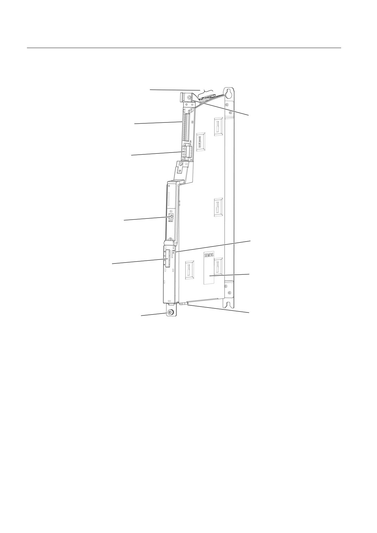
Illustration
;
;
'5,9( &/L4 LQWHUIDFHV
;
;
6KLHOG VXSSRUW
;
'LJLWDO LQSXWV RXWSXWV
;
(OHFWURQLFV SRZHU VXSSO\
5(6(7 EXWWRQ
/('V
ჱ5'<
ჱ'3
7
7
7
0HDVXULQJ
7\SH SODWH
VRFNHWV
&RQQHFWLRQ
;
HTXLSRWHQWLDO ERQGLQJ
SURWHFWLYH FRQGXFWRU
6HULDO LQWHUIDFH
QR IXQFWLRQ
0
1P
Figure 9-1
Illustration of the NX10.3 / 15.3 (without cover)
NCU 7x0.3 PN, NCU 7x0.3B PN
84
Manual, 06/2014, 6FC5397-1EP40-5BA1
Connectable components
9.1 NX10.3 / NX15.3
Type plate
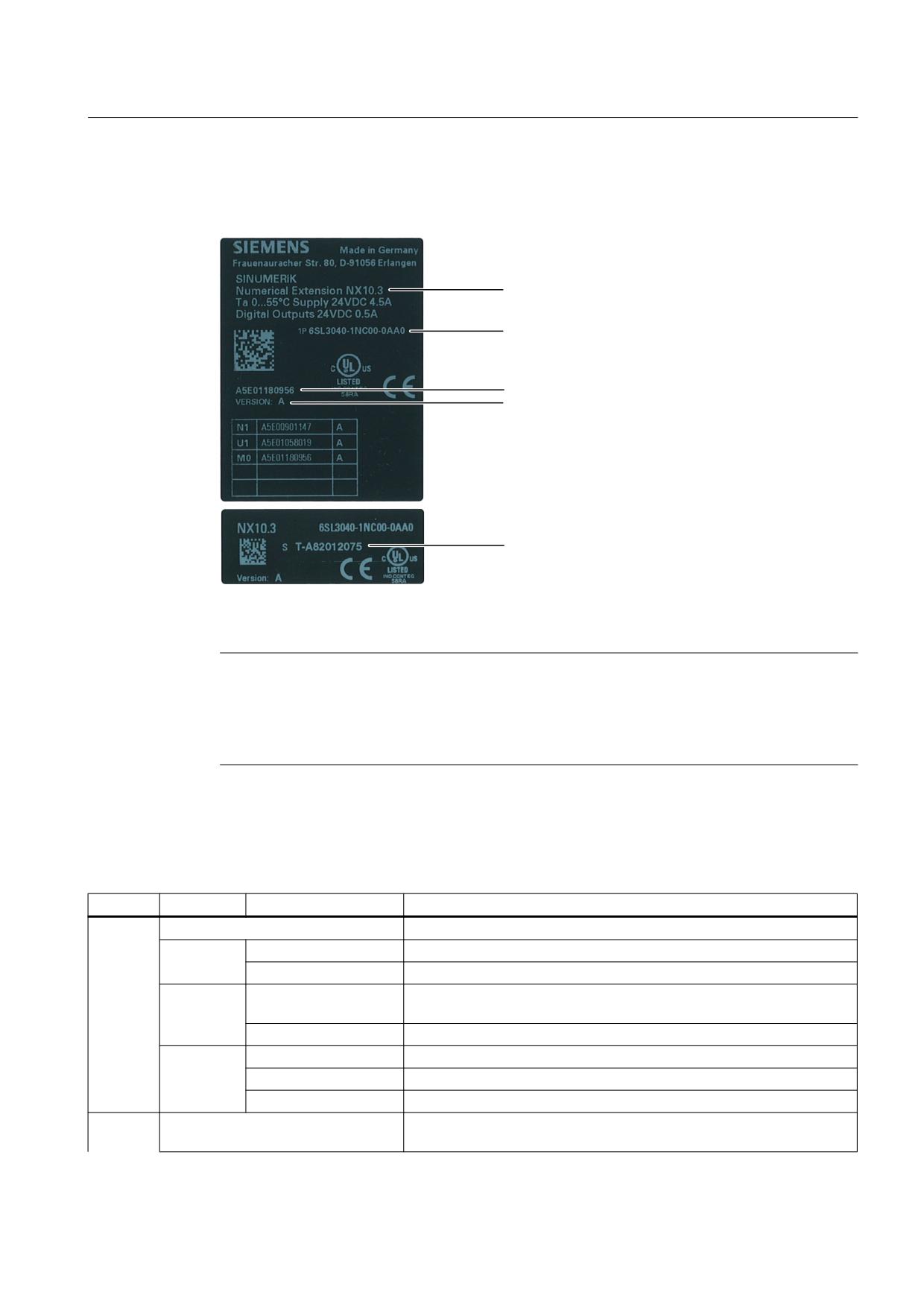
The NX module type plate contains the following basic information:
&RPSRQHQW QDPH
2UGHU QXPEHU
0DWHULDO QXPEHU
+: YHUVLRQ
6HULDO QXPEHU
Figure 9-2
Type plate using the NX10.3 as example
Note
You might need to access the information provided on the side-mounted type plate after the
equipment has been mounted. Since the type plate is located on the right-hand side of the
housing, which is the side typically used to connect to the SINAMICS S120 module, we
recommend that you make a note of the serial number of the NX prior to assembly.
LED displays
Table 9-1
Description of LEDs on the NX10.3 / 15.3
LED
Color
Status
Description
RDY
Off
Electronic power supply outside permissible tolerance range
Continuous light
NX is ready for operation
Green
Flashing light 2 Hz
Writing to CompactFlash card of the connected NCU
Continuous light
NX is presently booting and at least one fault is present (e.g. RESET,
Red
watchdog monitoring, basic system fault).
Flashing light 0.5 Hz
Boot error (e.g. firmware cannot be loaded into the RAM)
Orange
Continuous light
Firmware loading into RAM
Flashing light 0.5 Hz
Unable to load firmware into RAM
Flashing light 2 Hz
Firmware CRC fault
DP
Off
Electronics power supply outside the permissible tolerance range, NX is
not ready to run.
NCU 7x0.3 PN, NCU 7x0.3B PN
Manual, 06/2014, 6FC5397-1EP40-5BA1
85

Connectable components
9.1 NX10.3 / NX15.3
LED
Color
Status
Description
Green
Continuous light
CU_LINK is ready for communication and cyclic communication is
running.
Flashing light 0.5 Hz
CU_LINK is ready for communication and no cyclic communication is
running.
Red
Continuous light
At least one CU_LINK fault is present.
CU_LINK not ready for operation (e.g. after switching on)
RESET button
The RESET button is on the front of the module under the cover.
Note
When the pushbutton is actuated, the locally connected drive systems are brought to a
standstill with no feedback to the control. In other words, the drive and controller run
asynchronously once the drive has successfully booted up.
NCU 7x0.3 PN, NCU 7x0.3B PN
86
Manual, 06/2014, 6FC5397-1EP40-5BA1
Connectable components
9.1 NX10.3 / NX15.3
9.1.2
Dimension drawing
Figure 9-3
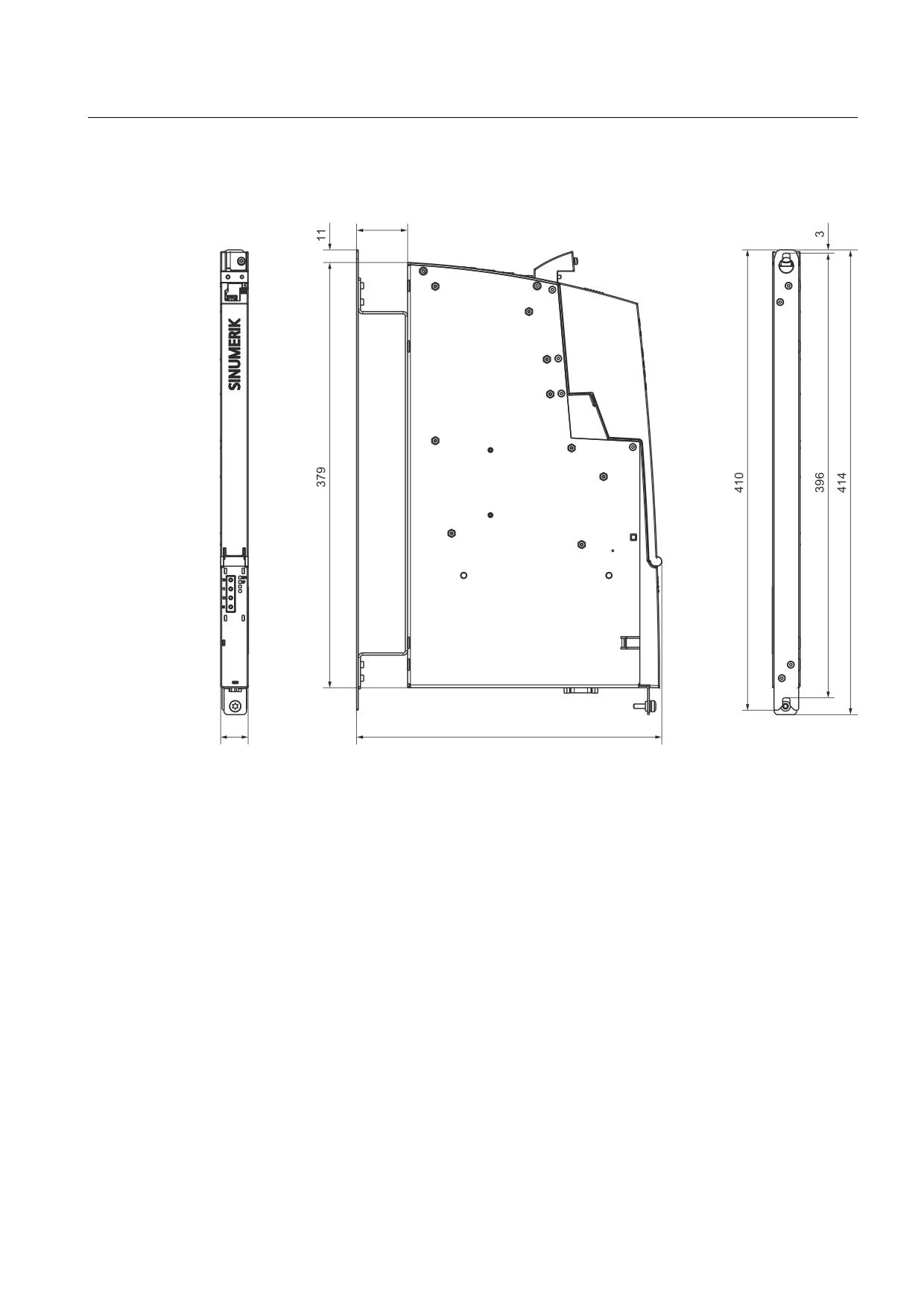
NX10.3 / 15.3 dimension drawing (dimensions in mm)
NCU 7x0.3 PN, NCU 7x0.3B PN
Manual, 06/2014, 6FC5397-1EP40-5BA1
87
Connectable components
9.1 NX10.3 / NX15.3
9.1.3
Mounting
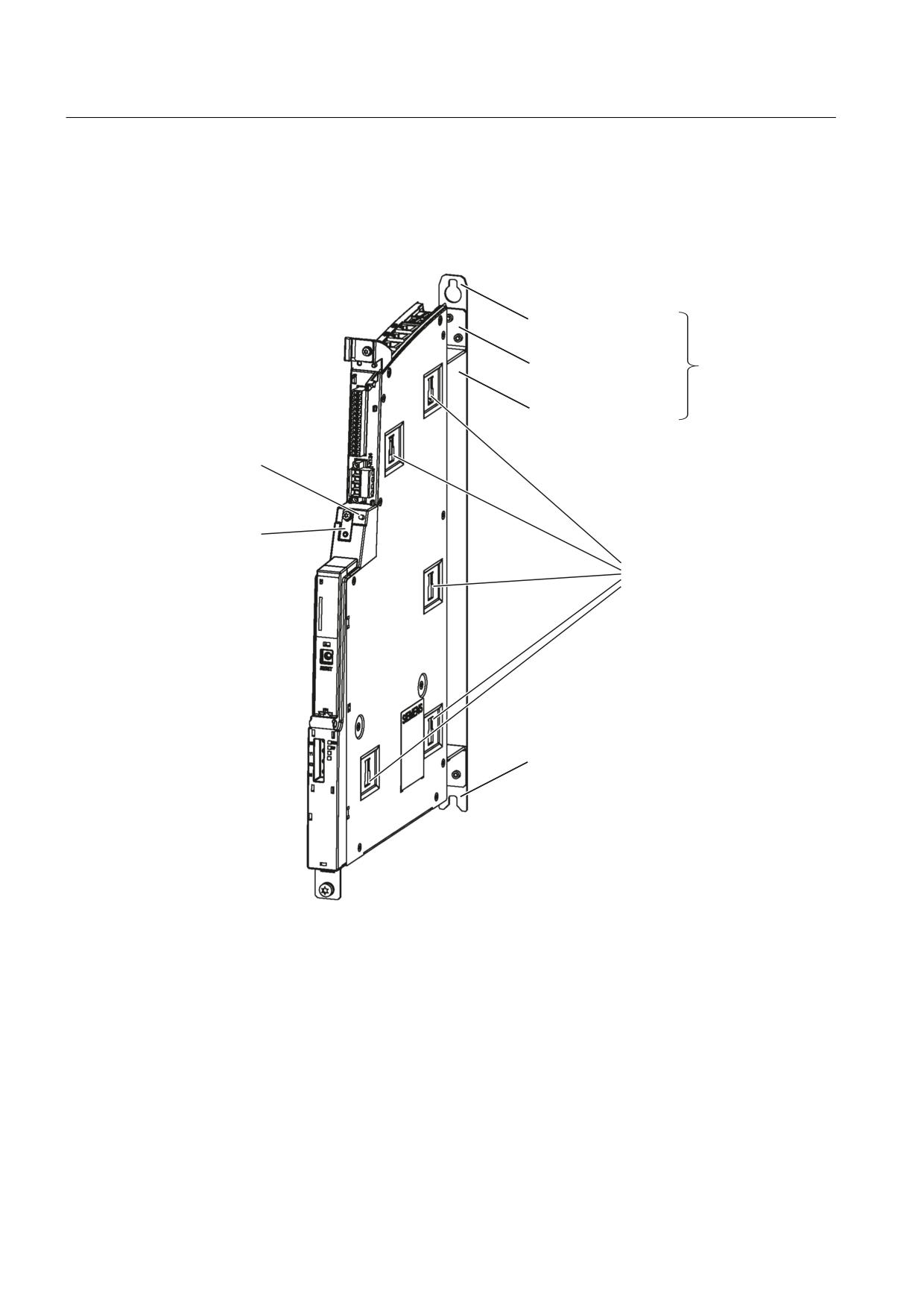
Mounting aids
)L[LQJ OXJ
$QJOH SODWH
6SDFHU
+ROGLQJ SODWH
3LQ
%UDFNHW
&XWRXWV IRU
ODWHUDO PRXQWLQJ
)L[LQJ OXJ
Figure 9-4
Mounting aids for the NX module
NCU 7x0.3 PN, NCU 7x0.3B PN
88
Manual, 06/2014, 6FC5397-1EP40-5BA1

Connectable components
9.1 NX10.3 / NX15.3
Designs
WARNING
Risk of fire through overheating if there are insufficient ventilation clearances
Inadequate ventilation clearances cause overheating with a risk for personnel due to smoke
and fire. Further, increased failures and shorter service life of the devices/systems can occur.
Under all circumstances, maintain a ventilation clearance of 80 mm above and below the NX
module.
An NX can be mounted in the control cabinet in the following ways:
NX on the side of the SINAMICS drive line-up
First, you must insert the supports into the cutouts of the NX that are attached to the Line
Module. Then the NX can be attached to the Line Module.
NX with spacer directly on the rear panel of the control cabinet - standard
The NX is secured with two M6 screws (6 Nm) to the mounting panel.
NX without spacer directly on the rear panel of the control cabinet
In addition, you can secure the NX directly on the rear panel of the control cabinet even without
spacers. Using this method, you must remove the spacer attached as standard when originally
supplied.
Note
The spacer is secured with M3 torx screws on the NX. You require a screwdriver T10 to attach/
remove the spacer.
1. Removing the holding plate.
2. Remove the angle plate.
3. Attach the holding plate to the NX using M3 screws (0.8 Nm).
4. Attach the NX with two M6 screws (6 Nm) to the mounting panel.
Mounting an NX to an additional NX
For stability reasons, you can connect the bracket of one NX to the clip of an adjacent NX:
1. Open the interface covers.
2. Release the screw fixing the bracket.
3. The bracket must be moved so that the pin is in the opening of the bracket. Tighten the
screw.
4. Close the interface covers.
NCU 7x0.3 PN, NCU 7x0.3B PN
Manual, 06/2014, 6FC5397-1EP40-5BA1
89
Connectable components
9.1 NX10.3 / NX15.3
9.1.4
Connection
Power supply X124
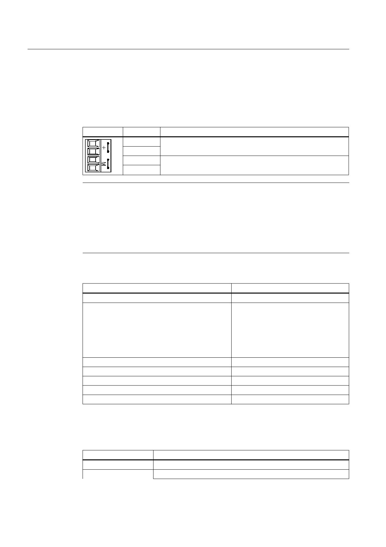
Table 9-2
Pin assignment for X124
Pin
Function
+
24 V DC power supply (20.4 V - 28.8 V)
+
M
Ground
M
Note
The two "+" and "M" terminals are jumpered in the connector and not in the device. This
ensures that the supply voltage is looped through.
The current consumption increases by the current consumption of DRIVE-CLiQ and the digital
outputs.
When using external power supplies (e.g. SITOP), the ground potential must be connected
with the protective ground terminal (PELV).
Table 9-3
Cable specification for X124
Features
Version
Connector type
4-pin screw terminal
Connectable cable types and conductor cross-sections
● Rigid
●
0.2 mm² to 2.5 mm²
● Flexible
●
0.2 mm² to 2.5 mm²
● Flexible, with end sleeve without plastic sleeve
●
0.2 mm² to 2.5 mm²
● Flexible, with end sleeve with plastic sleeve
●
0.2 mm² to 1.5 mm²
● AWG / kcmil
●
22 to 12
Stripped length
6-7 mm
Tool
Screwdriver 0.5 x 3 mm (M2.5)
Tightening torque
0.4 to 0.5 Nm
Max. current carrying capacity, incl. loop-through
20 A (15 A according to UL/CSA)
Max. cable length
10 m
DRIVE-CLiQ interfaces X100 - X103
Table 9-4
Characteristics of X100 - X103
Characteristic
Version
Connector type
DRIVE-CLiQ plug
Cable type
DRIVE-CLiQ standard (inside the control cabinet)
NCU 7x0.3 PN, NCU 7x0.3B PN
90
Manual, 06/2014, 6FC5397-1EP40-5BA1
Connectable components
9.1 NX10.3 / NX15.3
Characteristic
Version
MOTION CONNECT (outside the control cabinet)
Max. cable length
70 m
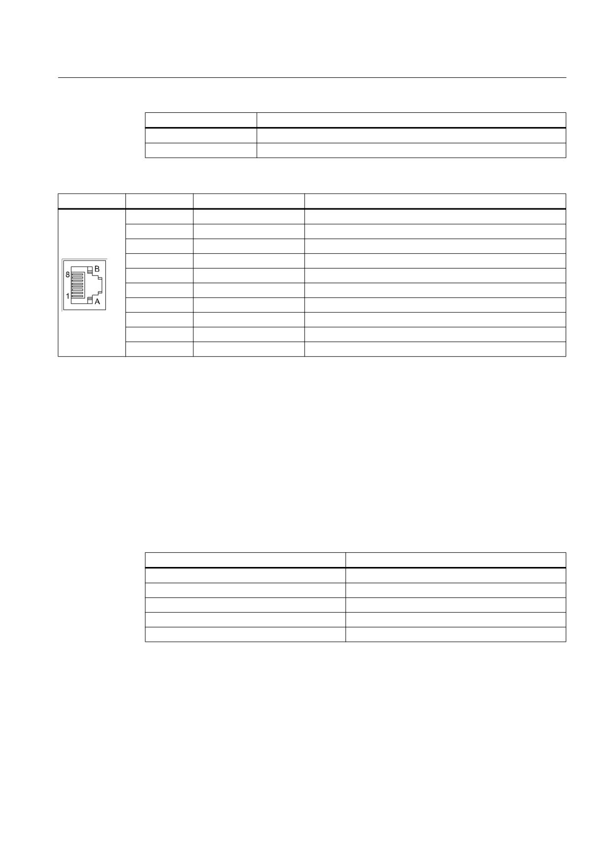
Table 9-5
Pin assignment, X100 - X103
Pin
Signal name
Technical specifications
1
TXP
Transmit data +
2
TXN
Transmit data -
3
RXP
Receive data +
4
-
Reserved, do not use
5
-
Reserved, do not use
6
RXN
Receive data -
7
-
Reserved, do not use
8
-
Reserved, do not use
A
+ (24 V)
Power supply
B
M (0 V)
Ground
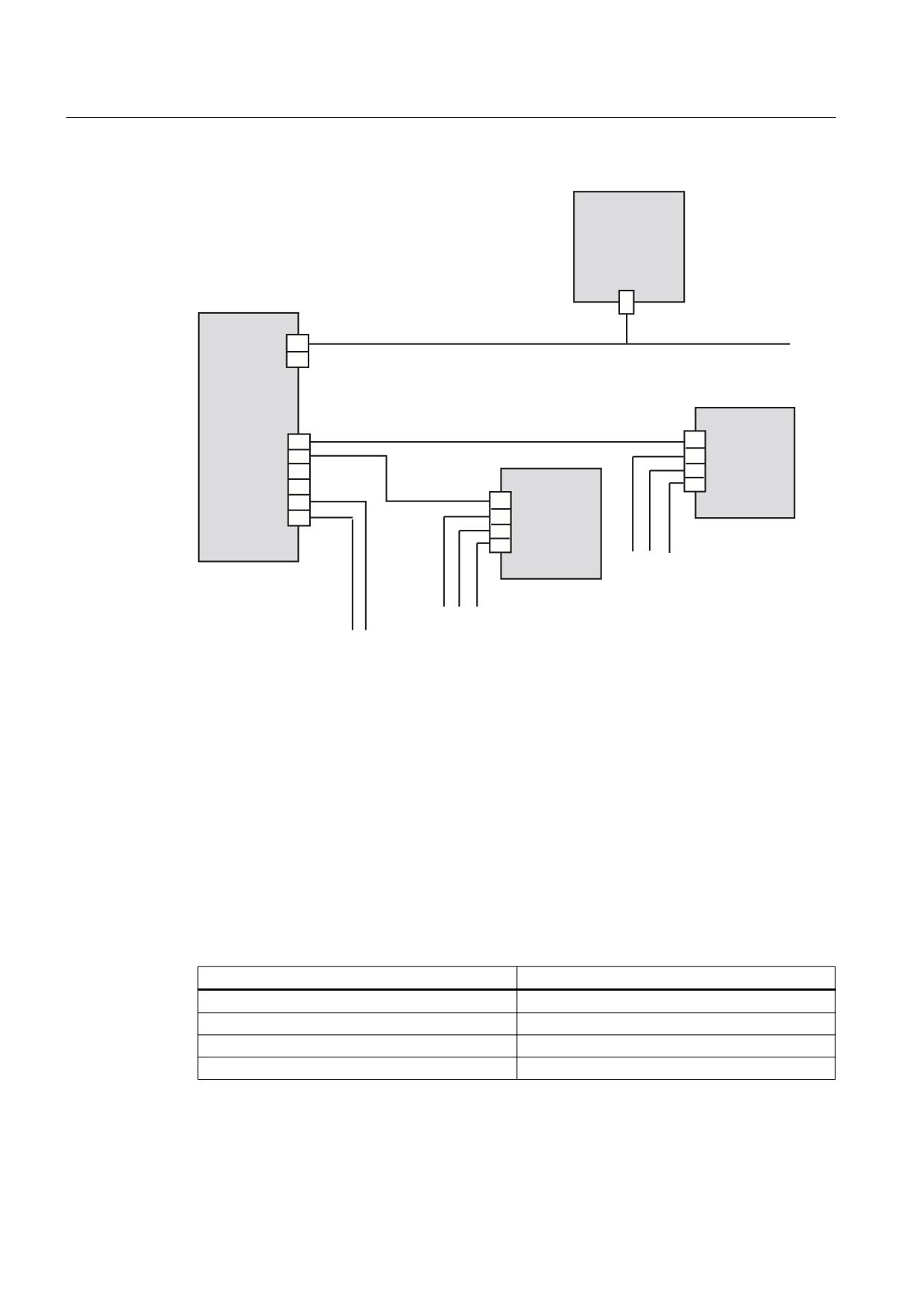
DRIVE-CLiQ topology
NX components can be connected to the NCU via DRIVE-CLiQ. The following rules apply for
the wiring:
● Only one star topology is permitted between the NX and the NCU. In this way, only one NX
can be operated per DRIVE-CLiQ port of an NCU.
● DRIVE-CLiQ ports not assigned to NX can be wired to other DRIVE-CLiQ components.
● Once an NX has been connected and configured, you cannot simply insert it into a different
DRIVE-CLiQ port, as the addresses of the integrated drives are set permanently from the
point of view of the PLC. The following table illustrates this relation:
Table 9-6
NX PROFIBUS addresses
DRIVE-CLiQ port on the NCU
Drive PROFIBUS addresses
X105
15
X104
14
X103
13
X102
12
X101
11
The following figure shows a sample topology:
NCU 7x0.3 PN, NCU 7x0.3B PN
Manual, 06/2014, 6FC5397-1EP40-5BA1
91
Connectable components
9.1 NX10.3 / NX15.3
(7
1&8
([WHUQDO 352),%86 '3 '3
;
;
1;
;
;
1;
;
;
'3 DGGUHVV
;
;
6XE WRSRORJ\ 1;
'3 DGGUHVV
6XE WRSRORJ\ 1;
'5,9( &/L4 FRPSRQHQWV RQ WKH 1&8
Figure 9-5
NX topology
X122 digital inputs/outputs
When commissioning the drive wizard, the digital inputs/outputs are correspondingly
preassigned functions.
For more information about terminal assignment, see:
● "Guidelines for machine configuration" System Manual, Chapter "Interfaces and their
terminal assignment"
● Commissioning Manual "IBN CNC: NCK, PLC, drive", Chapter "Communication interfaces
and terminal assignment"
Table 9-7
Interface characteristics of X122
Features
Version
Connector type
14-pin spring-loaded terminal
Connection option
0.2 to 1.5 mm2
Max. current carrying capacity
6 A
Max. cable length
30m
For details on the connection options, see Table 7-28 Connectable conductor cross-sections
(Page 75).
NCU 7x0.3 PN, NCU 7x0.3B PN
92
Manual, 06/2014, 6FC5397-1EP40-5BA1
Connectable components
9.1 NX10.3 / NX15.3
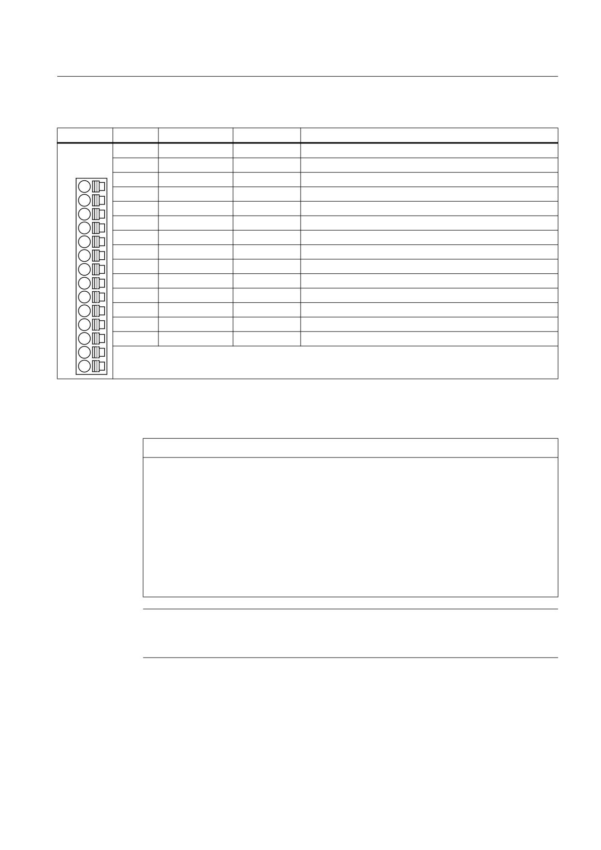
Table 9-8
Pin assignment for X122
Pin
Signal name
Signal type
Meaning
1
DI 0
I
Digital input 0
2
DI 1
I
Digital input 1
3
DI 2
I
Digital input 2
4
DI 3
I
Digital input 3
5
DI 16
I
Digital input 16
6
DI 17
I
Digital input 17
7
G1
GND
Ground for DI0 - DI3, DI16, DI17 (isolated with respect to M)
8
M
GND
Ground
9
DI/DO 8
B
Digital input/output 8 (rapid input)
10
DI/DO 9
B
Digital input/output 9 (rapid input)
11
M
GND
Ground
12
DI/DO 10
B
Digital input/output 10 (rapid input)
13
DI/DO 11
B
Digital input/output 11 (rapid input)
14
M
GND
Ground
Signal type: B = Bidirectional; I = Input; GND = Reference potential (ground)
DI: Digital input; DI/DO: Bidirectional digital input/output; M: Ground M1: Ground reference
Please take the technical data of the digital inputs/outputs from Chapter Technical data
(Page 76).
NOTICE
Ensuring the function of the digital inputs
An open input is interpreted as "low".
The "rapid inputs" can be used for position detection and as inputs of measuring inputs
depending on the terminal assignment used.
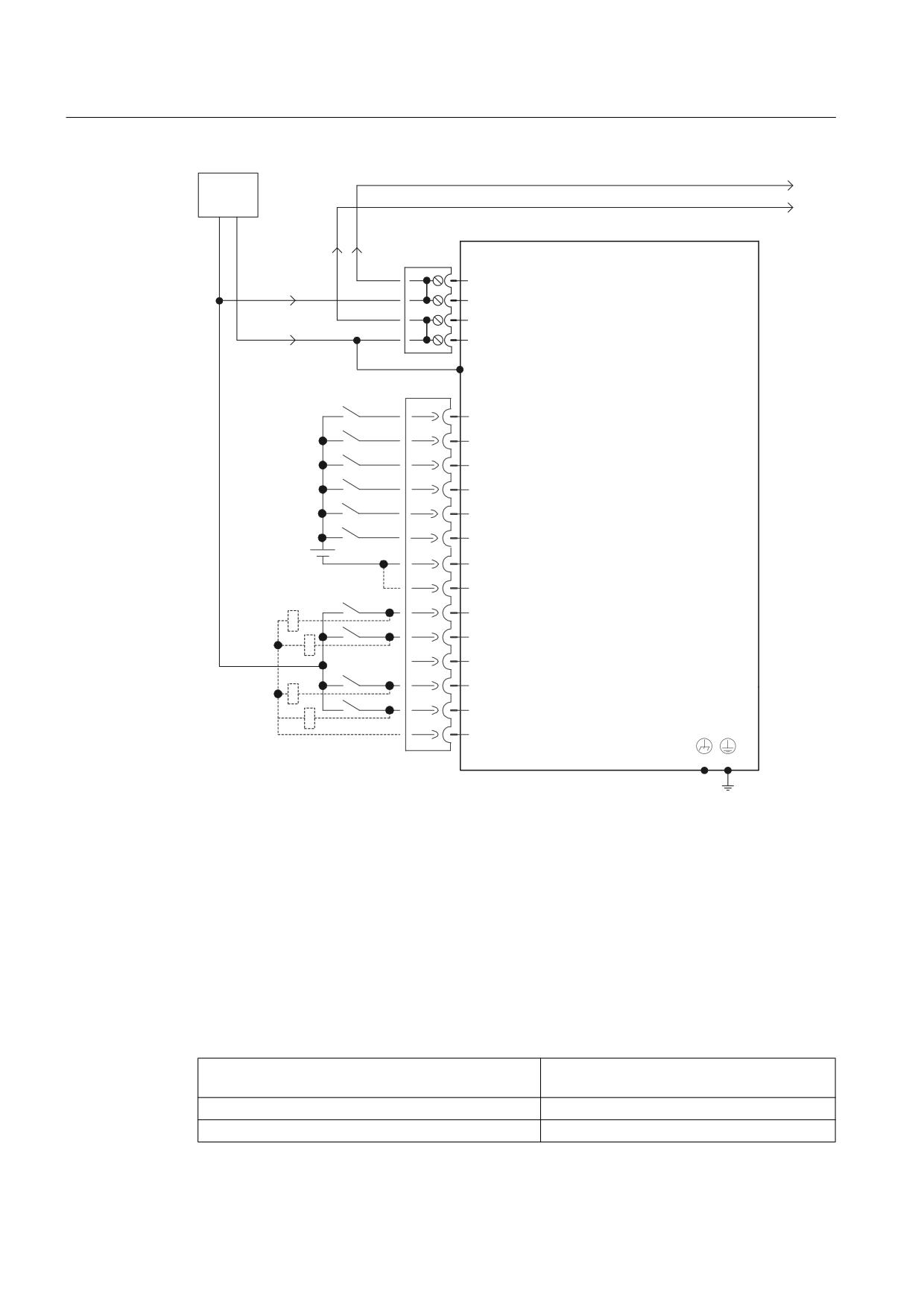
To enable digital inputs 0 to 3 to function, terminal M1 must be connected. This can be done
as follows:
● Connect the ground reference of the digital inputs.
● A jumper to terminal M (note that these digital inputs are then no longer electrically
isolated).
Note
For a transient (brief) voltage interruption of the 24 V supply, the digital outputs are switched
inactive for this time.
NCU 7x0.3 PN, NCU 7x0.3B PN
Manual, 06/2014, 6FC5397-1EP40-5BA1
93
Connectable components
9.1 NX10.3 / NX15.3
H[W
9 '&
0
0
;
9
1XPHULFDO ([WHQVLRQ 1;
0
0
0
0
;
',
5DSLG LQSXWV
PXVW EH VKLHOGHG
',
-XPSHU RSHQ HOHFWULFDO LVRODWLRQ
',
IRU GLJLWDO LQSXWV ',
',
&DQ EH SDUDPHWHUL]HG DV
',
LQSXW RXWSXW
',
0
0
', '2
', '2
0
', '2
', '2
0
Figure 9-6
Block diagram for digital inputs/outputs
Additional references
For information on commissioning NX components, please refer to the "Commissioning
Manual IBN CNC: NCK, PLC, drive".
9.1.5
Technical Data
Table 9-9
Safety-related data
Protection class according to EN 61800-5-1
Class I (with protective conductor system) and
Class III (PELV)
Degree of protection to EN 60529
IP20
Approvals
CE, cULus
NCU 7x0.3 PN, NCU 7x0.3B PN
94
Manual, 06/2014, 6FC5397-1EP40-5BA1

Connectable components
9.2 PP 72/48D PN
Pollution degree
2
Cooling
Open-circuit ventilation
Mounting position
Vertical
PE/ground connection
at the housing with M5 screw Torx / 3 Nm
Table 9-10
Electrical and mechanical data
Input voltage
24 V DC (20.4 - 28.8)
Current drain (without DRIVE-CLiQ and digital outputs)
0.3 A
Max. permitted output current
3.35 A
Power loss
15 W
Dimensions WxHxD (with spacers)
25 x 414 x 272 mm
Weight
2.58 kg
9.2
PP 72/48D PN
9.2.1
Description
Characteristics
I/O module PP 72/48D PN is a simple module (without a separate housing) for connecting
digital input/outputs as part of an automation system based on PROFINET IO.
The module has the following important features:
● PROFINET IO connection (max. 100 Mbits/s)
●
72 digital inputs and 48 digital outputs
● On-board status display via 2 diagnostic LEDs
● The 3 plug-in connectors for the digital inputs and outputs are 50-pin terminal posts for
connecting ribbon cables.
● Terminal strip converters can be used, or the direct connection of distribution boards, for
example, is possible.
An external power supply unit (24 V DC) is required to supply the module and the digital outputs.
NCU 7x0.3 PN, NCU 7x0.3B PN
Manual, 06/2014, 6FC5397-1EP40-5BA1
95
Connectable components
9.2 PP 72/48D PN
Illustration
352),1(7 ;
/('V
3RUW
3RUW
6
+
+
0RXQWLQJ SODWH
;
;
;
;
*URXQGLQJ VFUHZ
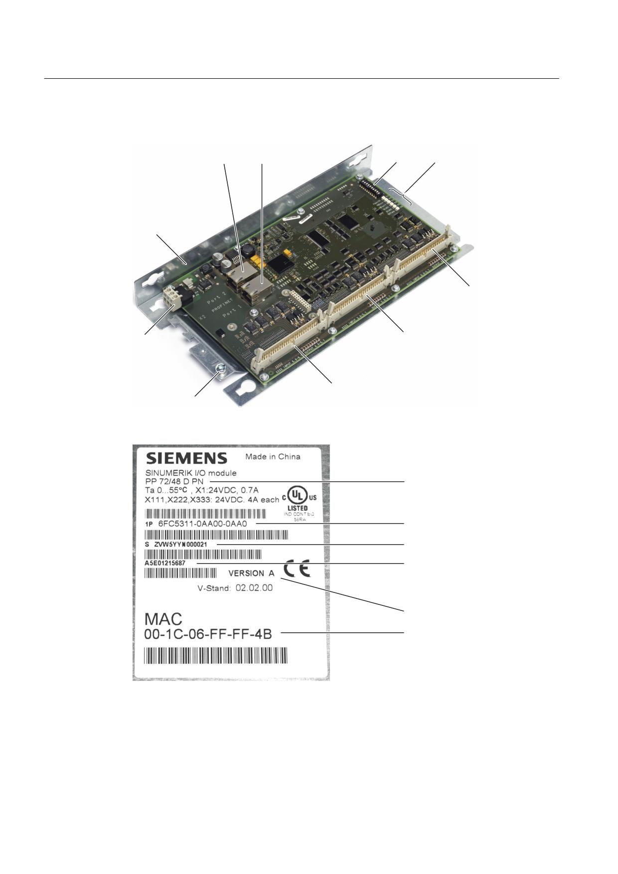
Figure 9-7
PP 72/48D PN I/O module
&RPSRQHQW QDPH
2UGHU QXPEHU
6HULDO QXPEHU
0DWHULDO QXPEHU
+: YHUVLRQ
0$& DGGUHVV
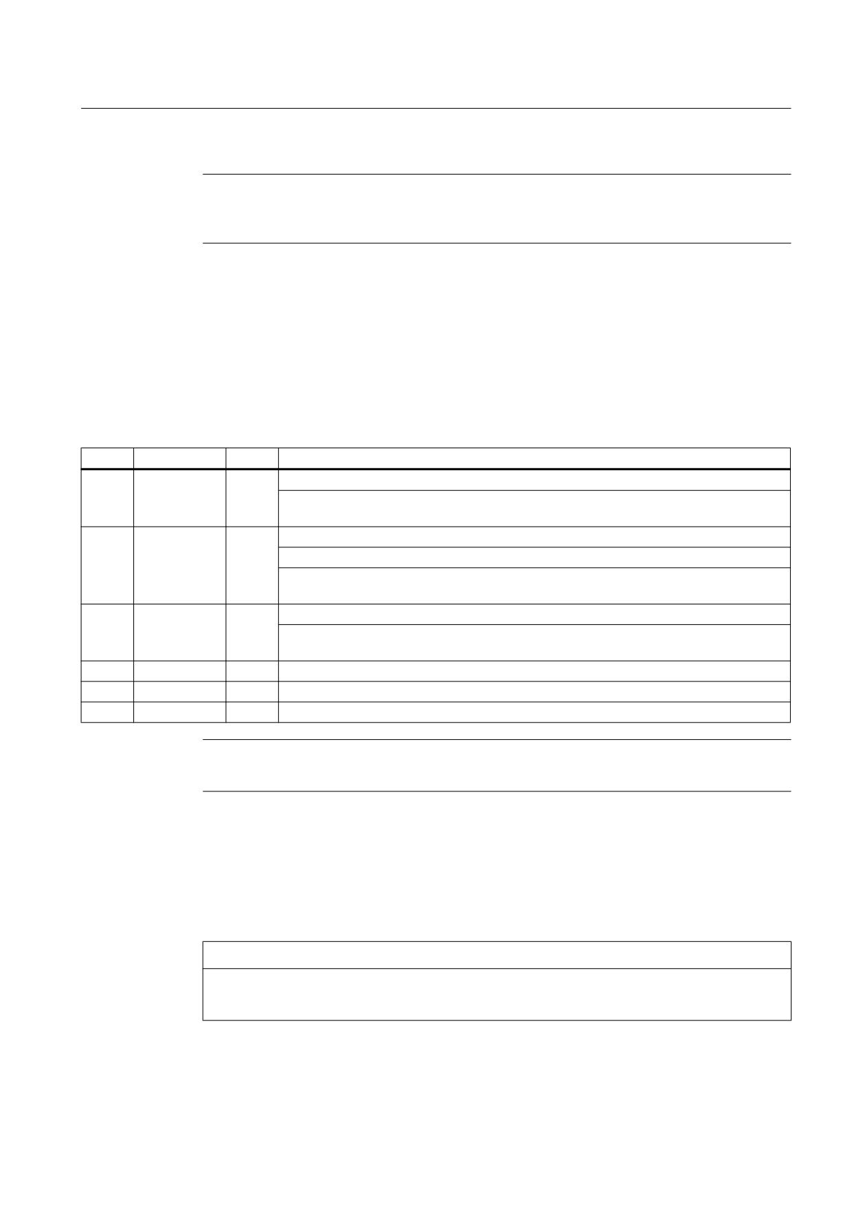
Figure 9-8
PP 72/48D PN type plate
NCU 7x0.3 PN, NCU 7x0.3B PN
96
Manual, 06/2014, 6FC5397-1EP40-5BA1
Connectable components
9.2 PP 72/48D PN
Note
The type plate is located on the rear side of the mounting plate. It is advisable to make a note
of relevant data as it is no longer visible after installation.
LED displays
Each PROFINET port has two integrated LEDs displaying the link status (green) and activity
(orange); see chapter Application (Page 58).
The PP 72/48 D PN has the following additional LEDs, which provide information on the module
status:
Table 9-11
LEDs: Status display
Name
Designation
Color
Description
H1
PowerOK
Green
Lit: Power supply ok
Off: As soon as one of the generated logic voltages falls below its setpoint, a reset is
triggered and the PowerOK LED goes out.
H2
PNSync
Green
Lit: Task system is synchronized to the bus cycle clock.
Off: Task system is not synchronized to the bus cycle clock.
Flashes 0.5 Hz: Task system has synchronized to the bus cycle clock and cyclic data
exchange is running.
H3
PNFault
Red
Off: Module is operating without error.
Lit: A system error has occurred (faulty module, incorrect parameterization by the
PROFINET controller, etc. ).
H4
DIAG1
Green
Reserved
H5
DIAG2
Green
Reserved
H6
OVTemp
Red
Overtemperature display
Note
When the system is booting, LEDs H1, H2 and H3 are lit.
9.2.2
Mounting
The I/O module can be fastened to the wall of the control cabinet using a mounting plate and
M6 screws. The module must be installed according to EN 60204.
NOTICE
The I/O module can be damaged if there is no ground connection
A protective conductor must be connected using the grounding screw.
NCU 7x0.3 PN, NCU 7x0.3B PN
Manual, 06/2014, 6FC5397-1EP40-5BA1
97
Connectable components
9.2 PP 72/48D PN
Note
The type plate is fitted to the rear side of the mounting plate. It is advisable to make a note
of relevant data as it is no longer visible after installation.
NCU 7x0.3 PN, NCU 7x0.3B PN
98
Manual, 06/2014, 6FC5397-1EP40-5BA1
Connectable components
9.2 PP 72/48D PN
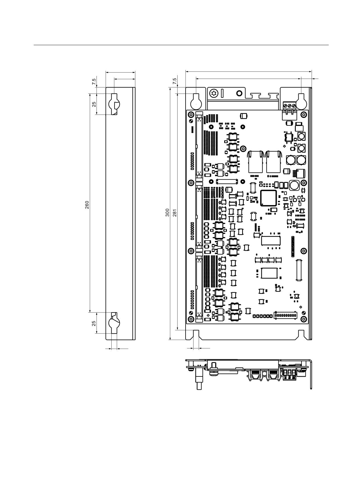
Figure 9-9
PP 72/48D PN dimension drawing
NCU 7x0.3 PN, NCU 7x0.3B PN
Manual, 06/2014, 6FC5397-1EP40-5BA1
99
Connectable components
9.2 PP 72/48D PN
9.2.3
Connecting
9.2.3.1
Interface overview
33
' 31
9 '&
;
3RZHU VXSSO\
1&8 [
31
352),1(7 FDEOH
;
352),1(7
3RUWVb DQG
33
' 31
0&3
&
& 31
;
5LEERQ FDEOH
'LJLWDO , 2
;
7HUPLQDO VWULS FRQYHUWHU
;
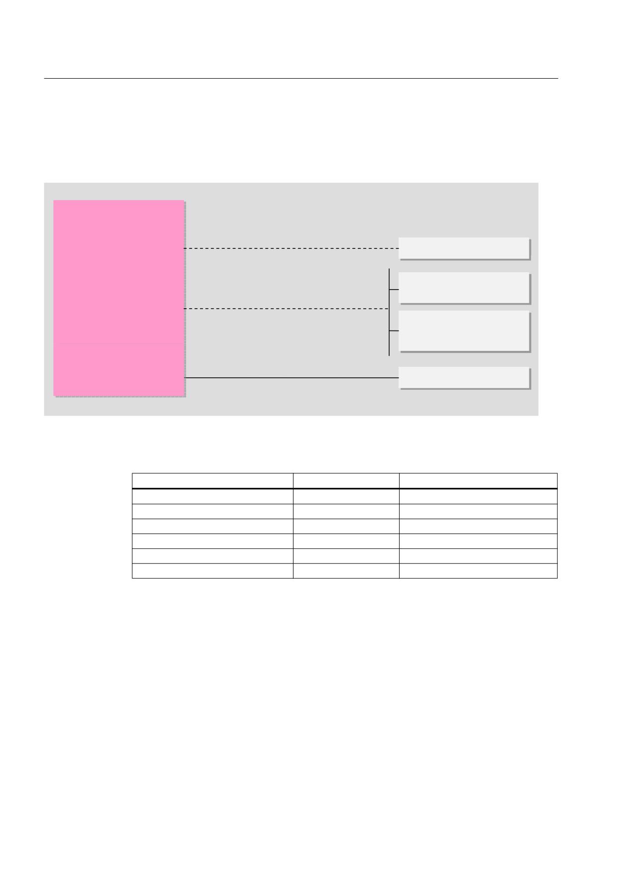
Figure 9-10 I/O module connection options
Table 9-12
PP 72/48D PN I/O module interfaces
Interface
Designation
Type
Power supply connection
X1
Screw-terminal block
PROFINET IO
X2 (ports 1 and 2)
Socket
PROFINET address
S1
DIP switch
Digital input/outputs 1
X111
Ribbon cable connector
Digital input/outputs 2
X222
Ribbon cable connector
Digital input/outputs 3
X333
Ribbon cable connector
9.2.3.2
X1 power supply
Properties
This interface is intended exclusively for the connection of the external 24 V power supply.
On the module side, the power supplies are protected against:
● Polarity reversal
● Short-circuit (elec. current limitation of the outputs)
● Overload (self-restoring PTC fuse - Multifuse)
NCU 7x0.3 PN, NCU 7x0.3B PN
100
Manual, 06/2014, 6FC5397-1EP40-5BA1
Connectable components
9.2 PP 72/48D PN
Requirements placed on the DC power supply
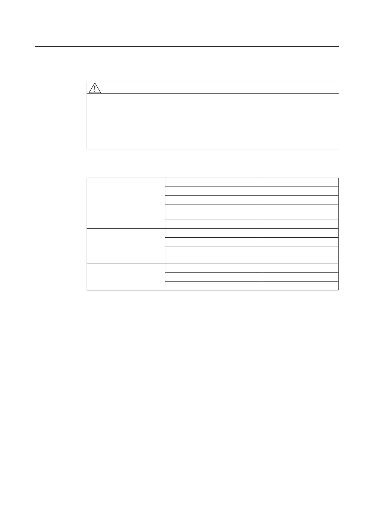
WARNING
Inadequately fused supply cables can be life-threatening
In the case of supply lines > 10 m, protectors must be installed at the device input in order
to protect against lightning (surge).
The DC power supply must be connected to the ground/shield of the I/O module for EMC
and/or functional reasons. For EMC reasons, this connection should only be made at one
point; see also EMC Installation Guide.
Table 9-13
Requirements of the DC power supply
Rated voltage
According to EN 61131-2
24 V DC
Voltage range (average value)
20.4 V DC to 28.8 V DC
Voltage range (dynamic)
18.5 to 30.2 V DC
Voltage ripple peak-to-peak
5% (unfiltered 6-pulse
rectification)
Booting time at POWER ON
Any
Non-periodic overvoltages
≤ 35 V
Duration of overvoltage
≤ 500 ms
Recovery time
≥ 50 s
Events per hour
≤ 10
Transient voltage interruptions
Outage time
≤ 3 ms
Recovery time
≥ 10 s
Events per hour
≤ 10
Digital inputs
The 24 V supplied at X1 are used to supply the 72 digital inputs.
If the internal supply voltage is not used to supply the digital inputs, this can optionally be
replaced by an external power supply (24 V DC). The reference ground of the power supply
source must each be connected with X111, X222, X333, pin 1 (GND). X111, X222, X333, pin
2 (P24OUT) then remains open.
Digital outputs
To supply (24 V DC) the digital outputs, an additional external power supply source is required.
The power supply is connected to terminals X111, X222 and X333 via pins 47, 48, 49 and 50
(DOCOMx). Ground pins must be connected to a common chassis ground.
NCU 7x0.3 PN, NCU 7x0.3B PN
Manual, 06/2014, 6FC5397-1EP40-5BA1
101

Connectable components
9.2 PP 72/48D PN
Maximum current consumption: 3 x 4 A if all outputs are used simultaneously.
Note
It is the user's responsibility to ensure that the max. current consumption per DOCOMx pin
(X111, X222, X333: Pins 47, 48, 49, 50) does not exceed 1 A. The power supply (+24 V DC)
for the digital outputs must therefore be connected to all 4 pins per DOCOMx (X111, X222,
X333: pins 47, 48, 49, 50).
Wiring the power supply
Table 9-14
Pin assignment at X1 screw-type terminal block
Pin
Signal name
Signal type
Meaning
1
P24
VI
24 V DC power supply
2
M
GND
Ground
3
PE
GND
Protective ground
Current requirement
0.7 A (at 24 V DC) for PP 72/48D PN and digital inputs plus 3 x 4 A at X111, X222 and X333
for supplying digital outputs.
Wiring the screw-type terminal block
The required 24 V DC load power supply is wired to the screw-type terminal block (X1).
DANGER
Danger of death caused by unsafe power supply
The 24 V direct voltage is to be configured as an extra-low voltage with protective separation
- DVC A or PELV according to EN 61800-5-1.
Power cables
Table 9-15
Cable specification at X1
Characteristics
Version
Connection option
Up to 2.5 mm2
Current carrying capacity
max. 10 A
Max. cable length
10 m
Use flexible cables with a cross-section of 0.25 to 2.5 mm2 (or AWG 23 to AWG 13) for wiring
the power supply according to the maximum current that flows.
If you only use one wire per connection, an end sleeve is not required.
You can use end sleeves without an insulating collar in accordance with DIN 46228, Form A
long version.
NCU 7x0.3 PN, NCU 7x0.3B PN
102
Manual, 06/2014, 6FC5397-1EP40-5BA1

Connectable components
9.2 PP 72/48D PN
9.2.3.3
X2 PROFINET
Data Transmission Rate and Cables
For PROFINET, you require a data transmission rate of 100 Mbit/s (Fast Ethernet). The
interfaces are designed for full-duplex mode; in other words, the ports can both transmit and
receive. For data transfer purposes you can use electrical twisted copper cables (twisted pair,
4-wire, 100Base-T):
● The transmission characteristics of these cables must meet the requirements of CAT5.
● The maximum length of the connections between the end device and network component
or between two network components (e.g. switch ports) must not exceed 100 m.
Pin assignment
Table 9-16
PROFINET interfaces X2, ports 1, 2
Pin
Signal name
Signal type
Meaning
1
TX+
O
Transmit data +
2
TX-
O
Transmit data -
3
RX+
I
Receive data +
4
N.C.
-
Reserved, do not use
5
N.C.
-
Reserved, do not use
6
RX-
I
Receive data -
7
N.C.
-
Reserved, do not use
8
N.C.
-
Reserved, do not use
Cable specification
Table 9-17
Cable specification at X2, ports 1, 2
Characteristic
Version
Connector type
RJ45 socket
Cable type
Industrial Ethernet cable (CAT5)
Max. cable length
100 m
LED displays
For diagnostic purposes, the RJ45 sockets are each equipped with a green and a yellow LED.
This allows the following information to be displayed for the respective PROFINET port:
Table 9-18
PROFINET ports LED displays
Name
Color
Status
Meaning
Link
Green
lit
Transfer rate 100 Mbit/s
off
No or faulty connection
NCU 7x0.3 PN, NCU 7x0.3B PN
Manual, 06/2014, 6FC5397-1EP40-5BA1
103
Connectable components
9.2 PP 72/48D PN
Name
Color
Status
Meaning
Activity
Orange
lit
Data exchange
off
No data exchange
PROFINET address (S1)
A logical address can be assigned to the I/O module for communication with PROFINET using
a 10-bit DIP switch S1.
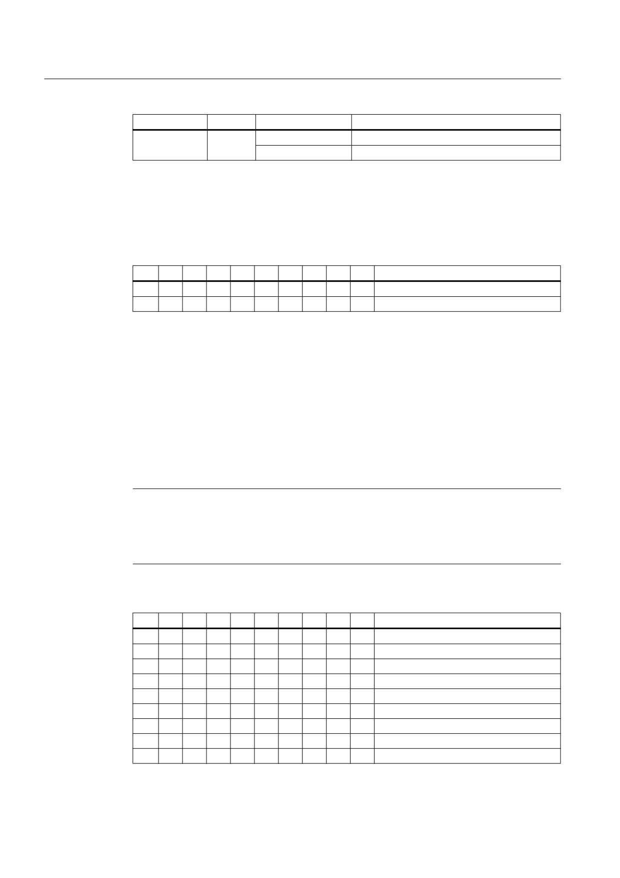
Table 9-19
General settings with switch S1
1
2
3
4
5
6
7
8
9
10
Meaning
on
on
PROFINET functionality
on
on
on
on
on
on
on
on
DCP mode
The switch positions 9 and 10 guarantee the PROFINET functionality of the module and must
always be switched "on".
DCP mode
In this mode, there is no default device name.
The device name must be set using initialization and remains saved on the I/O module. It is
first deleted when the factory setting is restored, e.g. using STEP7.
Default device names
The switch positions 1 to 8 define the default device name of the I/O module.
There are up to 128 default device names. If these default device names are used, there is no
need for initialization.
Note
The default device names cannot be reconfigured using the STEP7 "device initialization"
facility, for example.
If you are connecting the I/O module to a SINUMERIK controller as a PROFINET component,
make sure that this functionality is supported by the controller concerned.
Table 9-20
Default device name with switch S1
1
2
3
4
5
6
7
8
9
10
Default device name
on
on
on
on
on
on
on
off
pp72x48pn127
off
on
on
on
on
on
on
off
pp72x48pn126
on
off
on
on
on
on
on
off
pp72x48pn125
off
off
on
on
on
on
on
off
pp72x48pn124
on
on
off
on
on
on
on
off
pp72x48pn123
off
on
off
on
on
on
on
off
pp72x48pn122
on
off
off
on
on
on
on
off
pp72x48pn121
off
off
off
on
on
on
on
off
pp72x48pn120
NCU 7x0.3 PN, NCU 7x0.3B PN
104
Manual, 06/2014, 6FC5397-1EP40-5BA1

Connectable components
9.2 PP 72/48D PN
1
2
3
4
5
6
7
8
9
10
Default device name
on
on
on
off
on
on
on
off
pp72x48pn119
off
on
on
off
on
on
on
off
pp72x48pn118
on
off
on
off
on
on
on
off
pp72x48pn117
off
off
on
off
on
on
on
off
pp72x48pn116
on
on
off
off
on
on
on
off
pp72x48pn115
off
on
off
off
on
on
on
off
pp72x48pn114
on
off
off
off
on
on
on
off
pp72x48pn113
off
off
off
off
on
on
on
off
pp72x48pn112
x
x
x
x
x
x
x
x
"
on
on
on
on
off
off
off
off
pp72x48pn15
off
on
on
on
off
off
off
off
pp72x48pn14
on
off
on
on
off
off
off
off
pp72x48pn13
off
off
on
on
off
off
off
off
pp72x48pn12
on
on
off
on
off
off
off
off
pp72x48pn11
off
on
off
on
off
off
off
off
pp72x48pn10
on
off
off
on
off
off
off
off
pp72x48pn9
off
off
off
on
off
off
off
off
pp72x48pn8
on
on
on
off
off
off
off
off
pp72x48pn7
off
on
on
off
off
off
off
off
pp72x48pn6
on
off
on
off
off
off
off
off
pp72x48pn5
off
off
on
off
off
off
off
off
pp72x48pn4
on
on
off
off
off
off
off
off
pp72x48pn3
off
on
off
off
off
off
off
off
pp72x48pn2
on
off
off
off
off
off
off
off
pp72x48pn1
off
off
off
off
off
off
off
off
pp72x48pn
Note
A newly set PROFINET address will only come into effect after power OFF/ON.
9.2.3.4
X111, X222 and X333 digital inputs/outputs
Cable specification
● Connectors: 50-pin ribbon cable connectors
50-pin insulation displacement connectors with cable grip, ribbon cables and terminal
converters
are required for connecting digital inputs and outputs.
● The required connecting cables (ribbon cables) must be provided by the user.
● Max. cable length: 30 m
NCU 7x0.3 PN, NCU 7x0.3B PN
Manual, 06/2014, 6FC5397-1EP40-5BA1
105

Connectable components
9.2 PP 72/48D PN
Pin assignment
Table 9-21
Pin assignment X111
Pin
Signal name
Type
Pin
Signal name
Type
1
M
GND
2
P24OUT
VO
3
Input 0.0
I
4
Input 0.1
I
5
Input 0.2
I
6
Input 0.3
I
7
Input 0.4
I
8
Input 0.5
I
9
Input 0.6
I
10
Input 0.7
I
11
Input 1.0
I
12
Input 1.1
I
13
Input 1.2
I
14
Input 1.3
I
15
Input 1.4
I
16
Input 1.5
I
17
Input 1.6
I
18
Input 1.7
I
19
Input 2.0
I
20
Input 2.1
I
21
Input 2.2
I
22
Input 2.3
I
23
Input 2.4
I
24
Input 2.5
I
25
Input 2.6
I
26
Input 2.7
I
27
Not assigned
-
28
Not assigned
-
29
Not assigned
-
30
Not assigned
-
31
Output 0.0
O
32
Output 0.1
O
33
Output 0.2
O
34
Output 0.3
O
35
Output 0.4
O
36
Output 0.5
O
37
Output 0.6
O
38
Output 0.7
O
39
Output 1.0
O
40
Output 1.1
O
41
Output 1.2
O
42
Output 1.3
O
43
Output 1.4
O
44
Output 1.5
O
45
Output 1.6
O
46
Output 1.7
O
47
DOCOM1
VI
48
DOCOM1
VI
49
DOCOM1
VI
50
DOCOM1
VI
VI: Voltage input / VO: Voltage output
I: Signal input / O: Signal output / GND: Reference potential (ground)
Table 9-22
Pin assignment for X222
Pin
Signal name
Type
Pin
Signal name
Type
1
M
GND
2
P24OUT
VO
3
Input 3.0
I
4
Input 3.1
I
5
Input 3.2
I
6
Input 3.3
I
7
Input 3.4
I
8
Input 3.5
I
9
Input 3.6
I
10
Input 3.7
I
11
Input 4.0
I
12
Input 4.1
I
13
Input 4.2
I
14
Input 4.3
I
15
Input 4.4
I
16
Input 4.5
I
17
Input 4.6
I
18
Input 4.7
I
NCU 7x0.3 PN, NCU 7x0.3B PN
106
Manual, 06/2014, 6FC5397-1EP40-5BA1

Connectable components
9.2 PP 72/48D PN
Pin
Signal name
Type
Pin
Signal name
Type
19
Input 5.0
I
20
Input 5.1
I
21
Input 5.2
I
22
Input 5.3
I
23
Input 5.4
I
24
Input 5.5
I
25
Input 5.6
I
26
Input 5.7
I
27
Not assigned
-
28
Not assigned
-
29
Not assigned
-
30
Not assigned
-
31
Output 2.0
O
32
Output 2.1
O
33
Output 2.2
O
34
Output 2.3
O
35
Output 2.4
O
36
Output 2.5
O
37
Output 2.6
O
38
Output 2.7
O
39
Output 3.0
O
40
Output 3.1
O
41
Output 3.2
O
42
Output 3.3
O
43
Output 3.4
O
44
Output 3.5
O
45
Output 3.6
O
46
Output 3.7
O
47
DOCOM2
VI
48
DOCOM2
VI
49
DOCOM2
VI
50
DOCOM2
VI
VI: Voltage input / VO: Voltage output
I: Signal input / O: Signal output / GND: Reference potential (ground)
Table 9-23
Pin assignment for X333
Pin
Signal name
Type
Pin
Signal name
Type
1
M
GND
2
P24OUT
VO
3
Input 6.0
I
4
Input 6.1
I
5
Input 6.2
I
6
Input 6.3
I
7
Input 6.4
I
8
Input 6.5
I
9
Input 6.6
I
10
Input 6.7
I
11
Input 7.0
I
12
Input 7.1
I
13
Input 7.2
I
14
Input 7.3
I
15
Input 7.4
I
16
Input 7.5
I
17
Input 7.6
I
18
Input 7.7
I
19
Input 8.0
I
20
Input 8.1
I
21
Input 8.2
I
22
Input 8.3
I
23
Input 8.4
I
24
Input 8.5
I
25
Input 8.6
I
26
Input 8.7
I
27
Not assigned
-
28
Not assigned
-
29
Not assigned
-
30
Not assigned
-
31
Output 4.0
O
32
Output 4.1
O
33
Output 4.2
O
34
Output 4.3
O
35
Output 4.4
O
36
Output 4.5
O
37
Output 4.6
O
38
Output 4.7
O
39
Output 5.0
O
40
Output 5.1
O
41
Output 5.2
O
42
Output 5.3
O
NCU 7x0.3 PN, NCU 7x0.3B PN
Manual, 06/2014, 6FC5397-1EP40-5BA1
107
Connectable components
9.2 PP 72/48D PN
Pin
Signal name
Type
Pin
Signal name
Type
43
Output 5.4
O
44
Output 5.5
O
45
Output 5.6
O
46
Output 5.7
O
47
DOCOM3
VI
48
DOCOM3
VI
49
DOCOM3
VI
50
DOCOM3
VI
VI: Voltage input / VO: Voltage output
I: Signal input / O: Signal output / GND: Reference potential (ground)
Digital inputs
● Characteristics:
- X222: Inputs 3.0 to 3.7 are connected as rapid inputs; this means the input filter has a
max. delay time of 600 μs.
- The inputs have no signaling (status LEDs).
- The inputs are not isolated.
- It is not possible to connect 2-wire BEROs.
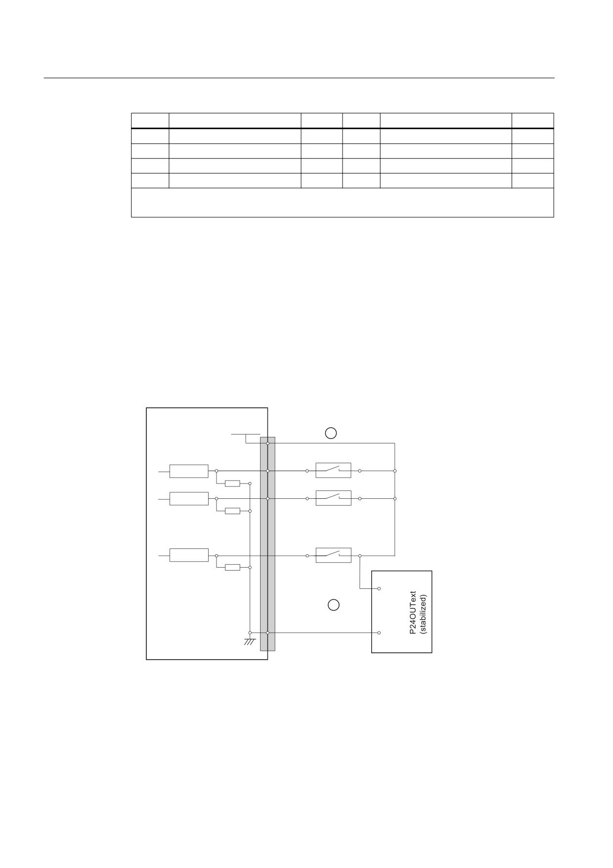
● Terminal assignment for the digital inputs:
The following figure shows an example of the terminal assignment for the digital inputs on
connector X111. Connectors X222 and X333 are assigned analogously.
;
;
;
33
' 31
3
287
3LQ QXPEHU
9'&
5HFHLYHU
5HFHLYHU
5HFHLYHU
9
9
0
([W SRZHU VXSSO\
① when using the internal power supply P24OUT
② when using an external power supply P24OUText
Figure 9-11 Terminal assignment for the digital inputs
NCU 7x0.3 PN, NCU 7x0.3B PN
108
Manual, 06/2014, 6FC5397-1EP40-5BA1

Connectable components
9.2 PP 72/48D PN
● Internal power supply (P24OUT):
The internal power supply for the digital inputs (X111, X222, X333: Pin 2) is derived from
the general power supply of module X1, pin 2 (P24).
● Technical data:
Table 9-24
Electrical specification of the digital inputs:
Digital inputs
min.
max.
Nominal
High-level voltage (UH)
15 V
30 V
24 V
Input current IIN at VH
2 mA
15 mA
-
Low-level voltage (UL)
-3 V
5 V
0 V
Signal delay time TPHL
0.5 ms
3 ms
-
NCU 7x0.3 PN, NCU 7x0.3B PN
Manual, 06/2014, 6FC5397-1EP40-5BA1
109
Connectable components
9.2 PP 72/48D PN
Digital outputs
●
Characteristics
- No galvanic isolation.
- Protection against: Short-circuit, overtemperature, and loss of ground.
- Automatic disconnection in case of undervoltage.
●
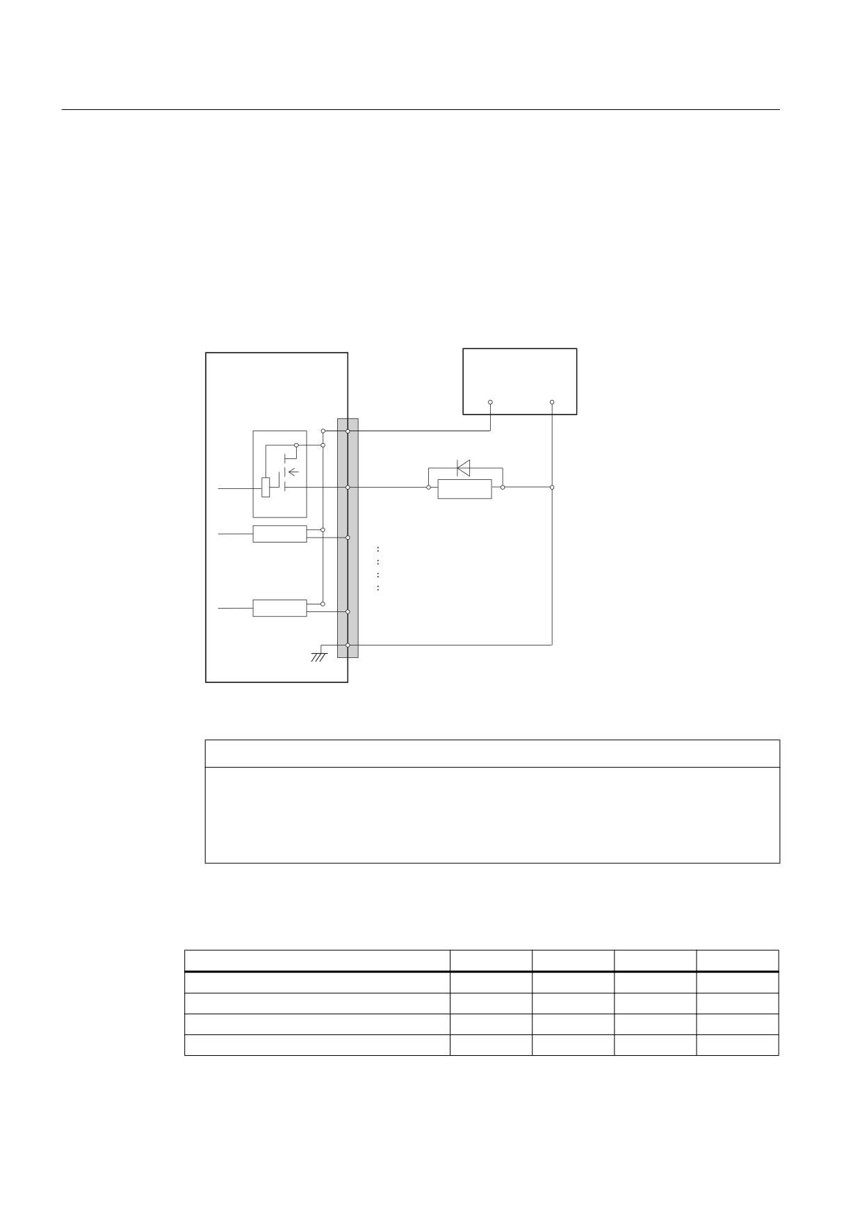
Terminal assignment for the digital outputs:
The following figure shows an example of the terminal assignment for the digital outputs
on connector X111. Connectors X222 and X333 are assigned analogously.
([W SRZHU VXSSO\
9 '& VWDELOL]HG
33
' 31
;
;
;
9
9
3LQ QXPEHU
'2&20[
5HOD\
'ULYHU
'ULYHU
:
:
:
:
'ULYHU
1 (M)
0
Figure 9-12 Terminal assignment for the digital outputs
NOTICE
Damage to the module
If the outputs are overloaded, the heat can melt the contacts.
Therefore, for a demand factor of 100%, a max. current of Iout = 0.25 A at X111, X222,
X333: Pin 2, must not be exceeded.
●
Technical data:
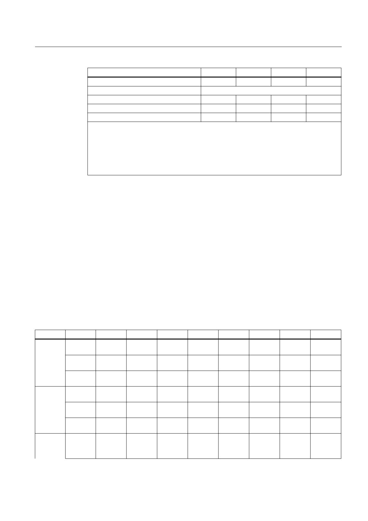
Table 9-25
Electrical specification of the digital outputs
Digital outputs
min.
Standard
max.
Nominal
1)
High-level voltage (UH)
VCC - 3 V
VCC
24 V
Output current IOUT
-
-
250 mA 2)
-
Voltage with low level (UL)
-
-
-
Output open
Leakage current at low level
-
50 μA
400 μA
-
NCU 7x0.3 PN, NCU 7x0.3B PN
110
Manual, 06/2014, 6FC5397-1EP40-5BA1
Connectable components
9.2 PP 72/48D PN
Digital outputs
min.
Standard
max.
Nominal
Signal delay time TPHL
-
0.5 ms
-
-
Maximum switching frequency
Resistive load
-
-
100 Hz
-
Inductive load
-
-
2 Hz
-
Lamp
-
-
11 Hz
-
●
1) UH_typical = VCC - IOUT × RON
VCC: Current operating voltage
IOUT: Output current
Maximum short-circuit current: 4 A (max. 100 μs, VCC = 24 V)
RON: Maximum internal resistance = 0.4 Ω
●
2) Where demand factor is 100% (all outputs active)
● Incorrect connection causes neither high level nor destruction of the outputs.
9.2.4
Parameter assignment
9.2.4.1
Input / output images
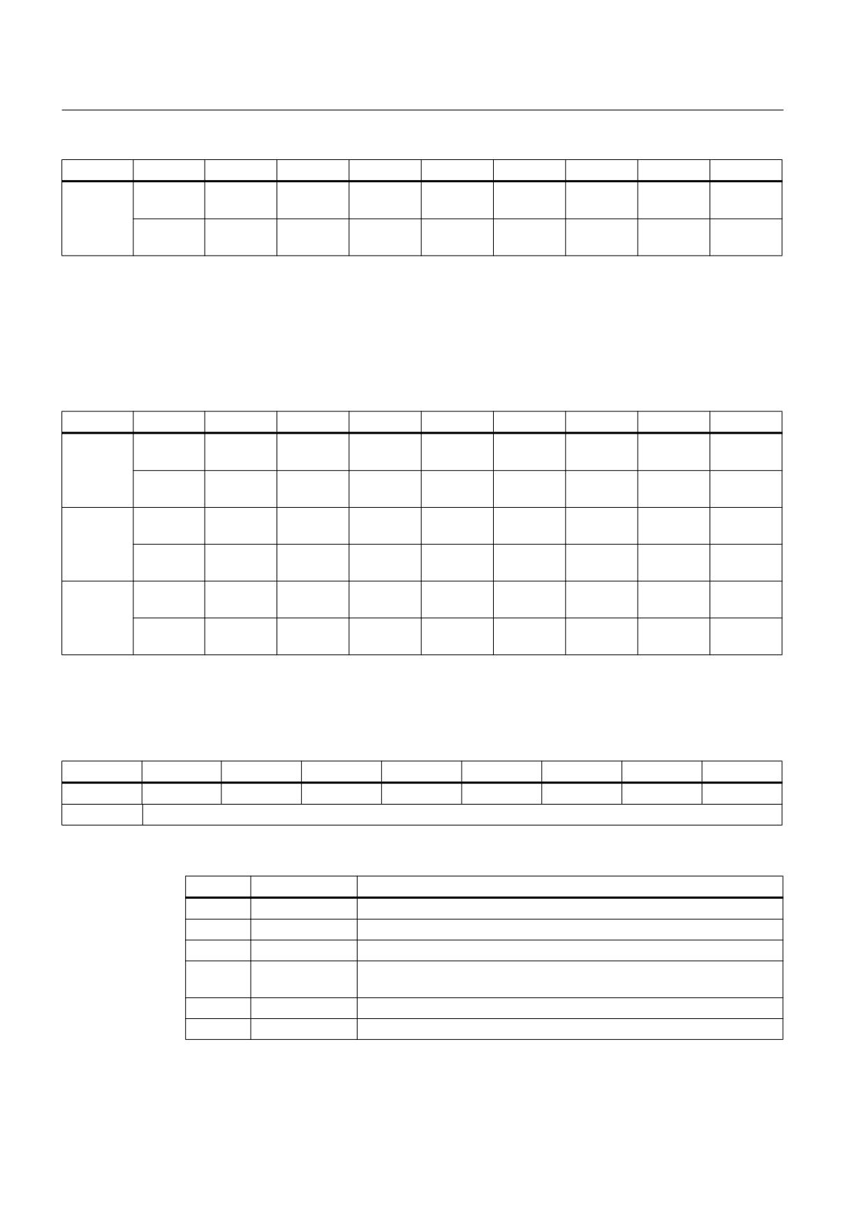
Input image
The image comprises 2 slots (n, d ≙ start address):
● Slot 1: Digital inputs (DI)
- n+0 … n+8 (9 byte)
- X222.P3 - .P10 are rapid inputs
● Slot 2: Diagnostics: d+0 .. d+1
Table 9-26
Input image of digital inputs for the 1st I/O module (n=0)
Terminal
Byte
Bit7
Bit6
Bit5
Bit4
Bit3
Bit2
Bit1
Bit0
n+0
Pin10
Pin9
Pin8
Pin7
Pin6
Pin5
Pin4
Pin3
DI 0.7
DI 0.6
DI 0.5
DI 0.4
DI 0.3
DI 0.2
DI 0.1
DI 0.0
n+1
Pin18
Pin17
Pin16
Pin15
Pin14
Pin13
Pin12
Pin11
X111
DI 1.7
DI 1.6
DI 1.5
DI 1.4
DI 1.3
DI 1.2
DI 1.1
DI 1.0
n+2
Pin26
Pin25
Pin24
Pin23
Pin22
Pin21
Pin20
Pin19
DI 2.7
DI 2.6
DI 2.5
DI 2.4
DI 2.3
DI 2.2
DI 2.1
DI 2.0
n+3
Pin10
Pin9
Pin8
Pin7
Pin6
Pin5
Pin4
Pin3
DI 3.7
DI 3.6
DI 3.5
DI 3.4
DI 3.3
DI 3.2
DI 3.1
DI 3.0
n+4
Pin18
Pin17
Pin16
Pin15
Pin14
Pin13
Pin12
Pin11
X222
DI 4.7
DI 4.6
DI 4.5
DI 4.4
DI 4.3
DI 4.2
DI 4.1
DI 4.0
n+5
Pin26
Pin25
Pin24
Pin23
Pin22
Pin21
Pin20
Pin19
DI 5.7
DI 5.6
DI 5.5
DI 5.4
DI 5.3
DI 5.2
DI 5.1
DI 5.0
n+6
Pin10
Pin9
Pin8
Pin7
Pin6
Pin5
Pin4
Pin3
DI 6.7
DI 6.6
DI 6.5
DI 6.4
DI 6.3
DI 6.2
DI 6.1
DI 6.0
X333
NCU 7x0.3 PN, NCU 7x0.3B PN
Manual, 06/2014, 6FC5397-1EP40-5BA1
111
Connectable components
9.2 PP 72/48D PN
Terminal
Byte
Bit7
Bit6
Bit5
Bit4
Bit3
Bit2
Bit1
Bit0
n+7
Pin18
Pin17
Pin16
Pin15
Pin14
Pin13
Pin12
Pin11
DI 7.7
DI 7.6
DI 7.5
DI 7.4
DI 7.3
DI 7.2
DI 7.1
DI 7.0
n+8
Pin26
Pin25
Pin24
Pin23
Pin22
Pin21
Pin20
Pin19
DI 8.7
DI 8.6
DI 8.5
DI 8.4
DI 8.3
DI 8.2
DI 8.1
DI 8.0
Output image
The image comprises one slot (n ≙ start address):
Digital outputs (DO): n+0 … n+5 (6 byte)
Table 9-27
Output image of digital outputs for the 1st I/O module (n=0)
Terminal
Byte
Bit7
Bit6
Bit5
Bit4
Bit3
Bit2
Bit1
Bit0
n+0
Pin38
Pin37
Pin36
Pin35
Pin34
Pin33
Pin32
Pin31
DO 0.7
DO 0.6
DO 0.5
DO 0.4
DO 0.3
DO 0.2
DO 0.1
DO 0.0
X111
n+1
Pin46
Pin45
Pin44
Pin43
Pin42
Pin41
Pin40
Pin39
DO 1.7
DO 1.6
DO 1.5
DO 1.4
DO 1.3
DO 1.2
DO 1.1
DO 1.0
n+2
Pin38
Pin37
Pin36
Pin35
Pin34
Pin33
Pin32
Pin31
DO 2.7
DO 2.6
DO 2.5
DO 2.4
DO 2.3
DO 2.2
DO 2.1
DO 2.0
X222
n+3
Pin46
Pin45
Pin44
Pin43
Pin42
Pin41
Pin40
Pin39
DO 3.7
DO 3.6
DO 3.5
DO 3.4
DO 3.3
DO 3.2
DO 3.1
DO 3.0
n+4
Pin38
Pin37
Pin36
Pin35
Pin34
Pin33
Pin32
Pin31
DO 4.7
DO 4.6
DO 4.5
DO 4.4
DO 4.3
DO 4.2
DO 4.1
DO 4.0
X333
n+5
Pin46
Pin45
Pin44
Pin43
Pin42
Pin41
Pin40
Pin39
DO 5.7
DO 5.6
DO 5.5
DO 5.4
DO 5.3
DO 5.2
DO 5.1
DO 5.0
9.2.4.2
Diagnostics via input image
Table 9-28
Diagnostics input image
Byte
Bit7
Bit6
Bit5
Bit4
Bit3
Bit3
Bit1
Bit0
d+0
count_2
count_1
count_0
T_Alarm_2
T_Alarm_1
Diag_2
Diag_1
Diag_0
d+1
Status_1
Table 9-29
Messages in byte 0
Bit
Signal name
Message
7
count_2
alive and well 2
6
count_1
alive and well 1
5
count_0
alive and well 0
4
T_Alarm_2
Temperature not within the operating temperature range defined for the
module
3
T_Alarm_1
Critical temperature exceeded
2
Diag_2
Overload DO byte 5/4
NCU 7x0.3 PN, NCU 7x0.3B PN
112
Manual, 06/2014, 6FC5397-1EP40-5BA1
Connectable components
9.2 PP 72/48D PN
Bit
Signal name
Message
1
Diag_1
Overload DO byte 3/2
0
Diag_0
Overload DO byte 1/0
Note
The "alive and well" counter is a 3 bit modulo counter at the PP application level. The PP
application can be monitored using this counter. Failure of the application software does not
generally result in a communication failure, as this is developed in a hardware-supported
manner. The watch dog switches off the digital outputs, while the inputs remain at their last
set values.
Table 9-30
Messages in byte 1, depending on the "alive and well" counter
"alive and
Value
Message
well" counter
byte 1
0
0
Reserved
1
Temperature value
2
5
Internal error, system error
Effect: The "PNFault" LED is activated. The outputs are disabled. The value
0x80 is stored in status byte 1.
Remedy: Switch the module off and on again.
3 ... 7
0
Reserved
9.2.5
Technical data
Table 9-31
Technical data of the I/O module
Safety
Degree of protection
IP 00 according to EN 60529
Protection class
III; DVC A, (PELV) acc. to EN 61800-5-1
Approvals
cULus, CE
Power consumption at rated load (without digital outputs)
PP 72/48D PN
17 W
PP 72/48D 2/2A PN
19 W
Mechanical data
Dimensions WxHxD
150 x 300 x 35 mm
Weight, approx.
0.9 kg
NCU 7x0.3 PN, NCU 7x0.3B PN
Manual, 06/2014, 6FC5397-1EP40-5BA1
113
Connectable components
9.3 PP 72/48D 2/2A PN
9.3
PP 72/48D 2/2A PN
9.3.1
Description
Characteristics
The I/O module is a simple module (without a separate enclosure) for connecting digital and
analog input/outputs as part of an automation system based on PROFINET IO.
The module has the following important features:
●
72 digital inputs and 48 digital outputs
●
2 analog inputs and 2 analog outputs
Analog process signals such as for detecting temperatures or controlling hydraulic
workholders can be implemented via analog inputs/outputs.
● PROFINET IO connection (max. 100 Mbits/s)
● On-board status display via 6 LEDs
● The 3 plug-in connectors for the digital inputs and outputs are 50-pin terminal posts for
connecting ribbon cables.
● Terminal strip converters can be used, or the direct connection of distribution boards, for
example, is possible.
● Analog signal cables can be connected directly to terminal contacts on the module.
An external power supply unit (24 V DC) is required to supply the module and the digital outputs.
NCU 7x0.3 PN, NCU 7x0.3B PN
114
Manual, 06/2014, 6FC5397-1EP40-5BA1
Connectable components
9.3 PP 72/48D 2/2A PN
Illustration
352),1(7 ;
3RUW
3RUW
6
/('V
+
+
;
;
;
;
6KLHOG FRQQHFWLRQ
;
*URXQGLQJ VFUHZ
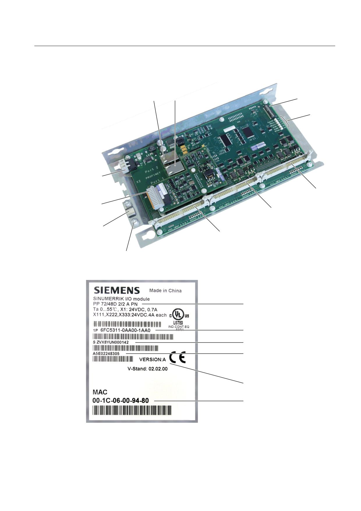
Figure 9-13 PP 72/48D 2/2A PN I/O module
&RPSRQHQW QDPH
2UGHU QXPEHU
6HULDO QXPEHU
0DWHULDO QXPEHU
+: YHUVLRQ
0$& DGGUHVV
Figure 9-14 PP 72/48D 2/2A PN type plate
NCU 7x0.3 PN, NCU 7x0.3B PN
Manual, 06/2014, 6FC5397-1EP40-5BA1
115
Connectable components
9.3 PP 72/48D 2/2A PN
Note
The type plate is located on the rear side of the mounting plate. It is advisable to make a note
of relevant data as it is no longer visible after installation.
LED displays
Each PROFINET port has two integrated LEDs displaying the link status (green) and activity
(orange); see chapter Application (Page 58).
The PP 72/48D 2/2A PN has the following LEDs, which provide information on the module
status.
Table 9-32
LEDs: Status display
Name
Designation
Color
Description
H1
PowerOK
Green
Lit: Power supply ok
Not lit: As soon as one of the generated logic voltages falls below its setpoint, a reset is
triggered and the PowerOK LED goes out.
H2
PNSync
Green
Lit: Task system is synchronized to the bus cycle clock.
Not lit: Task system is not synchronized to the bus cycle clock.
Flashes 0.5 Hz: Task system has synchronized to the bus cycle clock and cyclic data
exchange is running.
H3
PNFault
Red
Not lit: Module is operating without error.
Lit: A system error has occurred (faulty module, incorrect parameterization by the
PROFINET controller, etc. ).
H4
DIAG1
Green
Reserved
H5
DIAG2
Green
Reserved
H6
OVTemp
Red
Overtemperature display
Note
When the system is booting, LEDs H1, H2 and H3 are lit.
NCU 7x0.3 PN, NCU 7x0.3B PN
116
Manual, 06/2014, 6FC5397-1EP40-5BA1
Connectable components
9.3 PP 72/48D 2/2A PN
9.3.2
Dimension drawing
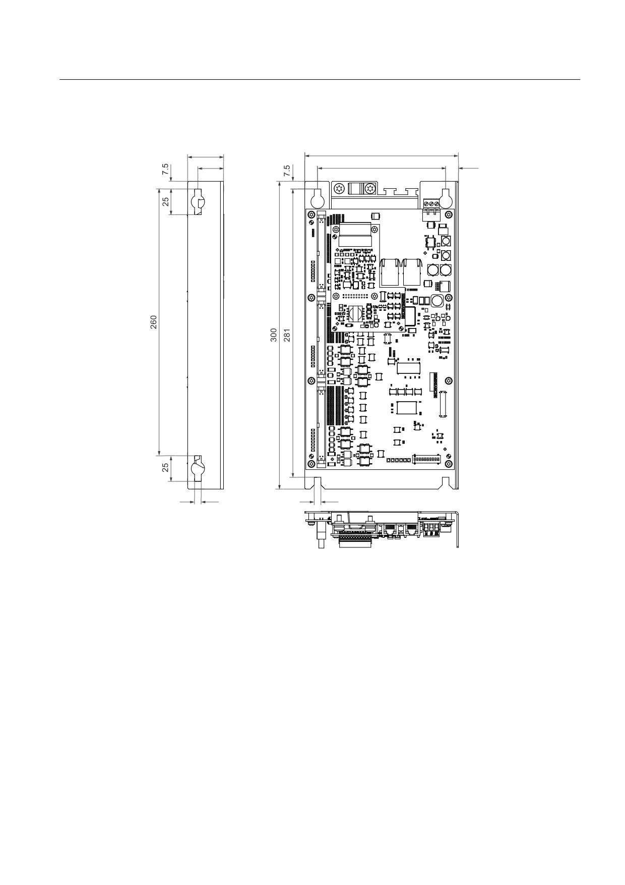
Figure 9-15 PP 72/48D 2/2A PN dimension drawing
9.3.3
Mounting
The PP 72/48D 2/2A PN I/O module is mounted just the same as the PP 72/48D PN, see
Mounting (Page 97).
NCU 7x0.3 PN, NCU 7x0.3B PN
Manual, 06/2014, 6FC5397-1EP40-5BA1
117
Connectable components
9.3 PP 72/48D 2/2A PN
9.3.4
Connection
9.3.4.1
Interface overview
2UGHU QR
3UHIDEULFDWHG FDEOHV
33
'
$ 31
9 '&
;
3RZHU VXSSO\
1&8 [
31
&RQQHFWLQJ FDEOH PD[
P
);
'&
;
352),1(7
3RUWV DQG
33
' 31
33
'
$ 31
0&3
&
& 31
;
5LEERQ FDEOH
'LJLWDO , 2
;
7HUPLQDO VWULS FRQYHUWHU
;
$QDORJ LQSXWV PD[
$QDORJ , 2
;
$QDORJ RXWSXWV PD[
Figure 9-16 Connection options of the PP 72/48D 2/2A PN I/O module
Interface overview
Table 9-33
Interfaces of the PP 72/48D 2/2A PN I/O module
Interface
Designation
Type
Power supply connection
X1
Screw-terminal block
PROFINET IO
X2 (ports 1 and 2)
Socket
Analog inputs/outputs
X3
Terminal block
PROFINET address
S1
DIP switch
Digital input/outputs 1
X111
Ribbon cable connector
Digital input/outputs 2
X222
Ribbon cable connector
Digital input/outputs 3
X333
Ribbon cable connector
The following abbreviations are used:
NCU 7x0.3 PN, NCU 7x0.3B PN
118
Manual, 06/2014, 6FC5397-1EP40-5BA1
Connectable components
9.3 PP 72/48D 2/2A PN
Signal type
Meaning
I
Input
O
Output
B
Bidirectional
V
Supply voltage
GND
Protective ground (reference potential)
Note
Digital and analog signals must not be laid together within a cable.
9.3.4.2
X1 power supply
Properties
This interface is intended exclusively for the connection of the external 24 V power supply.
On the module side, the power supplies are protected against:
● Polarity reversal
● Short-circuit (elec. current limitation of the outputs)
● Overload (self-restoring PTC fuse - Multifuse)
Requirements placed on the DC power supply
WARNING
Inadequately fused supply cables can be life-threatening
In the case of supply lines > 10 m, protectors must be installed at the device input in order
to protect against lightning (surge).
The DC power supply must be connected to the ground/shield of the I/O module for EMC
and/or functional reasons. For EMC reasons, this connection should only be made at one
point; see also EMC Installation Guide.
Table 9-34
Requirements of the DC power supply
Rated voltage
According to EN 61131-2
24 V DC
Voltage range (average value)
20.4 V DC to 28.8 V DC
Voltage range (dynamic)
18.5 to 30.2 V DC
Voltage ripple peak-to-peak
5% (unfiltered 6-pulse
rectification)
Booting time at POWER ON
Any
Non-periodic overvoltages
≤ 35 V
Duration of overvoltage
≤ 500 ms
NCU 7x0.3 PN, NCU 7x0.3B PN
Manual, 06/2014, 6FC5397-1EP40-5BA1
119
Connectable components
9.3 PP 72/48D 2/2A PN
Recovery time
≥ 50 s
Events per hour
≤ 10
Transient voltage interruptions
Outage time
≤ 3 ms
Recovery time
≥ 10 s
Events per hour
≤ 10
Digital inputs
The 24 V supplied at X1 are used to supply the 72 digital inputs.
If the internal supply voltage is not used to supply the digital inputs, this can optionally be
replaced by an external power supply (24 V DC). The reference ground of the power supply
source must each be connected with X111, X222, X333, pin 1 (GND). X111, X222, X333, pin
2 (P24OUT) then remains open.
Digital outputs
To supply (24 V DC) the digital outputs, an additional external power supply source is required.
The power supply is connected to terminals X111, X222 and X333 via pins 47, 48, 49 and 50
(DOCOMx). Ground pins must be connected to a common chassis ground.
Maximum current consumption: 3 x 4 A if all outputs are used simultaneously.
Note
It is the user's responsibility to ensure that the max. current consumption per DOCOMx pin
(X111, X222, X333: Pins 47, 48, 49, 50) does not exceed 1 A. The power supply (+24 V DC)
for the digital outputs must therefore be connected to all 4 pins per DOCOMx (X111, X222,
X333: pins 47, 48, 49, 50).
Analog inputs/outputs
The inputs and outputs are supplied with power on-board, i.e. no further external power supply
units are required.
Wiring the power supply
Table 9-35
Pin assignment at X1 screw-type terminal block
Pin
Signal name
Signal type
Meaning
1
P24
VI
24 V DC power supply
2
M
GND
Ground
3
PE
GND
Protective ground
Current requirement
0.7 A (at 24 V DC) for PP 72/48D 2/2A PN and digital inputs plus 3 x 4 A at X111, X222 and
X333 for supplying digital outputs.
NCU 7x0.3 PN, NCU 7x0.3B PN
120
Manual, 06/2014, 6FC5397-1EP40-5BA1
Connectable components
9.3 PP 72/48D 2/2A PN
Wiring the screw-type terminal block
The required 24 V DC load power supply is wired to the screw-type terminal block (X1).
DANGER
Danger of death caused by unsafe power supply
The 24 V direct voltage is to be configured as an extra-low voltage with protective separation
- DVC A or PELV according to EN 61800-5-1.
Power cables
Table 9-36
Cable specification at X1
Characteristics
Version
Connection option
Up to 2.5 mm2
Current carrying capacity
max. 10 A
Max. cable length
10 m
Use flexible cables with a cross-section of 0.25 to 2.5 mm2 (or AWG 23 to AWG 13) for wiring
the power supply according to the maximum current that flows.
If you only use one wire per connection, an end sleeve is not required.
You can use end sleeves without an insulating collar in accordance with DIN 46228, Form A
long version.
9.3.4.3
X2 PROFINET
Data Transmission Rate and Cables
For PROFINET, you require a data transmission rate of 100 Mbit/s (Fast Ethernet). The
interfaces are designed for full-duplex mode; in other words, the ports can both transmit and
receive. For data transfer purposes you can use electrical twisted copper cables (twisted pair,
4-wire, 100Base-T):
● The transmission characteristics of these cables must meet the requirements of CAT5.
● The maximum length of the connections between the end device and network component
or between two network components (e.g. switch ports) must not exceed 100 m.
Pin assignment
Table 9-37
PROFINET interfaces X2, ports 1, 2
Pin
Signal name
Signal type
Meaning
1
TX+
O
Transmit data +
2
TX-
O
Transmit data -
3
RX+
I
Receive data +
4
N.C.
-
Reserved, do not use
NCU 7x0.3 PN, NCU 7x0.3B PN
Manual, 06/2014, 6FC5397-1EP40-5BA1
121
Connectable components
9.3 PP 72/48D 2/2A PN
Pin
Signal name
Signal type
Meaning
5
N.C.
-
Reserved, do not use
6
RX-
I
Receive data -
7
N.C.
-
Reserved, do not use
8
N.C.
-
Reserved, do not use
Cable specification
Table 9-38
Cable specification at X2, ports 1, 2
Characteristic
Version
Connector type
RJ45 socket
Cable type
Industrial Ethernet cable (CAT5)
Max. cable length
100 m
LED displays
For diagnostic purposes, the RJ45 sockets are each equipped with a green and a yellow LED.
This allows the following information to be displayed for the respective PROFINET port:
Table 9-39
PROFINET ports LED displays
Name
Color
Status
Meaning
Link
Green
lit
Transfer rate 100 Mbit/s
off
No or faulty connection
Activity
Orange
lit
Data exchange
off
No data exchange
PROFINET address (S1)
A logical address can be assigned to the I/O module for communication with PROFINET using
a 10-bit DIP switch S1.
Table 9-40
General settings with switch S1
1
2
3
4
5
6
7
8
9
10
Meaning
on
on
PROFINET functionality
on
on
on
on
on
on
on
on
DCP mode
The switch positions 9 and 10 guarantee the PROFINET functionality of the module and must
always be switched "on".
DCP mode
In this mode, there is no default device name.
The device name must be set using initialization and remains saved on the I/O module. It is
first deleted when the factory setting is restored, e.g. using STEP7.
NCU 7x0.3 PN, NCU 7x0.3B PN
122
Manual, 06/2014, 6FC5397-1EP40-5BA1

Connectable components
9.3 PP 72/48D 2/2A PN
Default device names
The switch positions 1 to 8 define the default device name of the I/O module.
There are up to 128 default device names. If these default device names are used, there is no
need for initialization.
Note
The default device names cannot be reconfigured using the STEP7 "device initialization"
facility, for example.
If you are connecting the I/O module to a SINUMERIK controller as a PROFINET component,
make sure that this functionality is supported by the controller concerned.
Table 9-41
Default device name with switch S1
1
2
3
4
5
6
7
8
9
10
Default device name
on
on
on
on
on
on
on
off
pp72x48pn127
off
on
on
on
on
on
on
off
pp72x48pn126
on
off
on
on
on
on
on
off
pp72x48pn125
off
off
on
on
on
on
on
off
pp72x48pn124
on
on
off
on
on
on
on
off
pp72x48pn123
off
on
off
on
on
on
on
off
pp72x48pn122
on
off
off
on
on
on
on
off
pp72x48pn121
off
off
off
on
on
on
on
off
pp72x48pn120
on
on
on
off
on
on
on
off
pp72x48pn119
off
on
on
off
on
on
on
off
pp72x48pn118
on
off
on
off
on
on
on
off
pp72x48pn117
off
off
on
off
on
on
on
off
pp72x48pn116
on
on
off
off
on
on
on
off
pp72x48pn115
off
on
off
off
on
on
on
off
pp72x48pn114
on
off
off
off
on
on
on
off
pp72x48pn113
off
off
off
off
on
on
on
off
pp72x48pn112
x
x
x
x
x
x
x
x
"
on
on
on
on
off
off
off
off
pp72x48pn15
off
on
on
on
off
off
off
off
pp72x48pn14
on
off
on
on
off
off
off
off
pp72x48pn13
off
off
on
on
off
off
off
off
pp72x48pn12
on
on
off
on
off
off
off
off
pp72x48pn11
off
on
off
on
off
off
off
off
pp72x48pn10
on
off
off
on
off
off
off
off
pp72x48pn9
off
off
off
on
off
off
off
off
pp72x48pn8
on
on
on
off
off
off
off
off
pp72x48pn7
off
on
on
off
off
off
off
off
pp72x48pn6
NCU 7x0.3 PN, NCU 7x0.3B PN
Manual, 06/2014, 6FC5397-1EP40-5BA1
123
Connectable components
9.3 PP 72/48D 2/2A PN
1
2
3
4
5
6
7
8
9
10
Default device name
on
off
on
off
off
off
off
off
pp72x48pn5
off
off
on
off
off
off
off
off
pp72x48pn4
on
on
off
off
off
off
off
off
pp72x48pn3
off
on
off
off
off
off
off
off
pp72x48pn2
on
off
off
off
off
off
off
off
pp72x48pn1
off
off
off
off
off
off
off
off
pp72x48pn
Note
A newly set PROFINET address will only come into effect after power OFF/ON.
9.3.4.4
X111, X222 and X333 digital inputs/outputs
Cable specification
● Connectors: 50-pin ribbon cable connectors
50-pin insulation displacement connectors with cable grip, ribbon cables and terminal
converters
are required for connecting digital inputs and outputs.
● The required connecting cables (ribbon cables) must be provided by the user.
● Max. cable length: 30 m
Pin assignment
Table 9-42
Pin assignment X111
Pin
Signal name
Type
Pin
Signal name
Type
1
M
GND
2
P24OUT
VO
3
DI 0.0
I
4
DI 0.1
I
5
DI 0.2
I
6
DI 0.3
I
7
DI 0.4
I
8
DI 0.5
I
9
DI 0.6
I
10
DI 0.7
I
11
DI 1.0
I
12
DI 1.1
I
13
DI 1.2
I
14
DI 1.3
I
15
DI 1.4
I
16
DI 1.5
I
17
DI 1.6
I
18
DI 1.7
I
19
DI 2.0
I
20
DI 2.1
I
21
DI 2.2
I
22
DI 2.3
I
23
DI 2.4
I
24
DI 2.5
I
25
DI 2.6
I
26
DI 2.7
I
27
Not assigned
-
28
Not assigned
-
29
Not assigned
-
30
Not assigned
-
NCU 7x0.3 PN, NCU 7x0.3B PN
124
Manual, 06/2014, 6FC5397-1EP40-5BA1

Connectable components
9.3 PP 72/48D 2/2A PN
Pin
Signal name
Type
Pin
Signal name
Type
31
DO 0.0
O
32
DO 0.1
O
33
DO 0.2
O
34
DO 0.3
O
35
DO 0.4
O
36
DO 0.5
O
37
DO 0.6
O
38
DO 0.7
O
39
DO 1.0
O
40
DO 1.1
O
41
DO 1.2
O
42
DO 1.3
O
43
DO 1.4
O
44
DO 1.5
O
45
DO 1.6
O
46
DO 1.7
O
47
DOCOM1
VI
48
DOCOM1
VI
49
DOCOM1
VI
50
DOCOM1
VI
VI: Voltage Input / VO: Voltage Output
I: Signal Input / O: Signal Output / GND: Reference potential (ground)
Table 9-43
Pin assignment for X222
Pin
Signal name
Type
Pin
Signal name
Type
1
M
GND
2
P24OUT
VO
3
DI 3.0
I
4
DI 3.1
I
5
DI 3.2
I
6
DI 3.3
I
7
DI 3.4
I
8
DI 3.5
I
9
DI 3.6
I
10
DI 3.7
I
11
DI 4.0
I
12
DI 4.1
I
13
DI 4.2
I
14
DI 4.3
I
15
DI 4.4
I
16
DI 4.5
I
17
DI 4.6
I
18
DI 4.7
I
19
DI 5.0
I
20
DI 5.1
I
21
DI 5.2
I
22
DI 5.3
I
23
DI 5.4
I
24
DI 5.5
I
25
DI 5.6
I
26
DI 5.7
I
27
Not assigned
-
28
Not assigned
-
29
Not assigned
-
30
Not assigned
-
31
DO 2.0
O
32
DO 2.1
O
33
DO 2.2
O
34
DO 2.3
O
35
DO 2.4
O
36
DO 2.5
O
37
DO 2.6
O
38
DO 2.7
O
39
DO 3.0
O
40
DO 3.1
O
41
DO 3.2
O
42
DO 3.3
O
43
DO 3.4
O
44
DO 3.5
O
45
DO 3.6
O
46
DO 3.7
O
47
DOCOM2
VI
48
DOCOM2
VI
49
DOCOM2
VI
50
DOCOM2
VI
VI: Voltage Input / VO: Voltage Output
I: Signal Input / O: Signal Output / GND: Reference potential (ground)
NCU 7x0.3 PN, NCU 7x0.3B PN
Manual, 06/2014, 6FC5397-1EP40-5BA1
125

Connectable components
9.3 PP 72/48D 2/2A PN
Table 9-44
Pin assignment for X333
Pin
Signal name
Type
Pin
Signal name
Type
1
M
GND
2
P24OUT
VO
3
DI 6.0
I
4
DI 6.1
I
5
DI 6.2
I
6
DI 6.3
I
7
DI 6.4
I
8
DI 6.5
I
9
DI 6.6
I
10
DI 6.7
I
11
DI 7.0
I
12
DI 7.1
I
13
DI 7.2
I
14
DI 7.3
I
15
DI 7.4
I
16
DI 7.5
I
17
DI 7.6
I
18
DI 7.7
I
19
DI 8.0
I
20
DI 8.1
I
21
DI 8.2
I
22
DI 8.3
I
23
DI 8.4
I
24
DI 8.5
I
25
DI 8.6
I
26
DI 8.7
I
27
Not assigned
-
28
Not assigned
-
29
Not assigned
-
30
Not assigned
-
31
DO 4.0
O
32
DO 4.1
O
33
DO 4.2
O
34
DO 4.3
O
35
DO 4.4
O
36
DO 4.5
O
37
DO 4.6
O
38
DO 4.7
O
39
DO 5.0
O
40
DO 5.1
O
41
DO 5.2
O
42
DO 5.3
O
43
DO 5.4
O
44
DO 5.5
O
45
DO 5.6
O
46
DO 5.7
O
47
DOCOM3
VI
48
DOCOM3
VI
49
DOCOM3
VI
50
DOCOM3
VI
VI: Voltage Input / VO: Voltage Output
I: Signal Input / O: Signal Output / GND: Reference potential (ground)
NCU 7x0.3 PN, NCU 7x0.3B PN
126
Manual, 06/2014, 6FC5397-1EP40-5BA1
Connectable components
9.3 PP 72/48D 2/2A PN
Digital inputs
● Characteristics:
- X222: DI 3.0 to 3.7 are connected as rapid inputs.
- The inputs have no signaling (status LEDs).
- The inputs are not isolated.
- It is not possible to connect 2-wire BEROs.
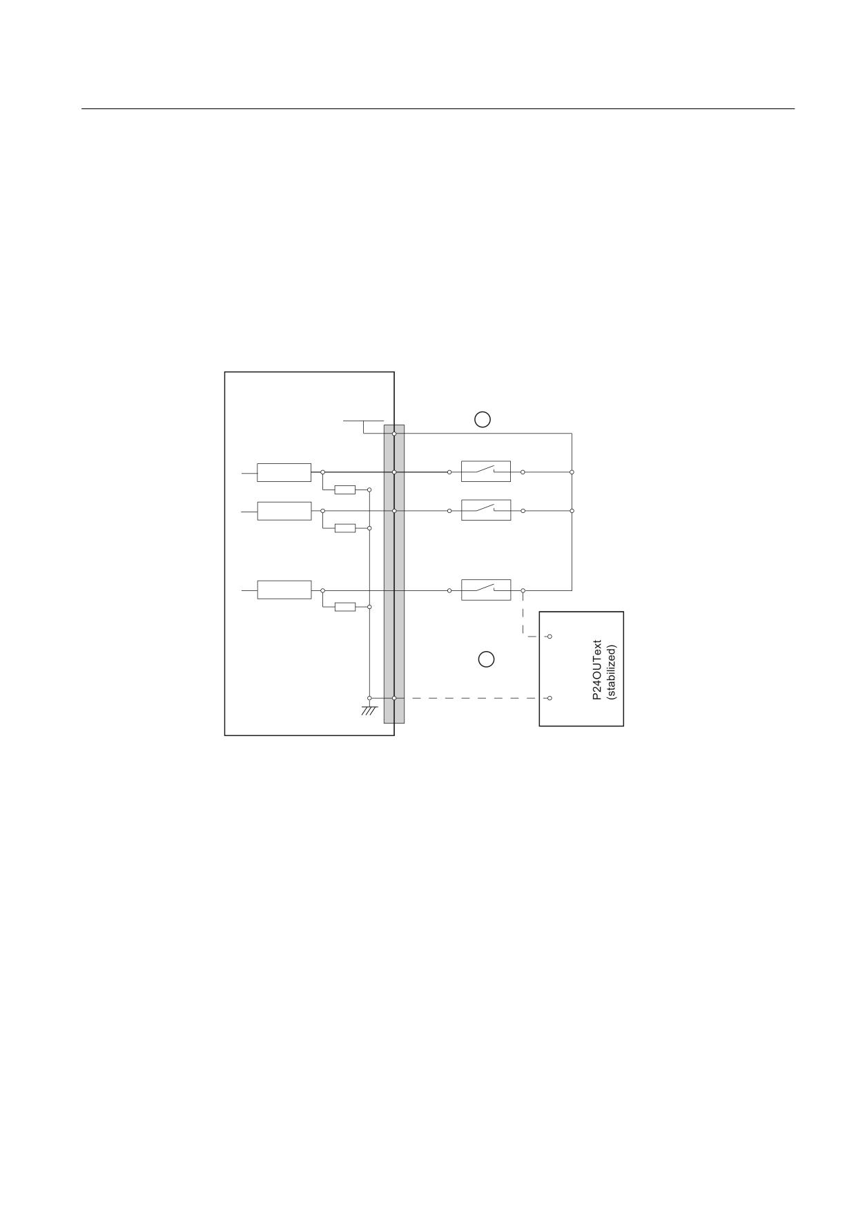
● Terminal assignment for the digital inputs:
The following figure shows an example of the terminal assignment for the digital inputs on
connector X111. Connectors X222 and X333 are assigned analogously.
33
'
$ 31
;
;
;
3
287
3LQ QXPEHU
9'&
5HFHLYHU
5HFHLYHU
5HFHLYHU
9
9
0
([W SRZHU VXSSO\
① when using the internal power supply P24OUT
② when using the external power supply P24OUText
Figure 9-17 Terminal assignment for the digital inputs
● Power supply for digital inputs (X111, X222, X333: Pin 2)
- The internal power supply (P24OUT) is taken from the general power supply of module
X1, pin 2 (P24).
- Alternatively, an external power supply can be connected if the load at the digital outputs
becomes too high.
● Technical data:
NCU 7x0.3 PN, NCU 7x0.3B PN
Manual, 06/2014, 6FC5397-1EP40-5BA1
127

Connectable components
9.3 PP 72/48D 2/2A PN
Table 9-45
Electrical specification of the digital inputs:
Digital inputs
min.
max.
Nominal
High-level voltage (UH)
15 V
30 V
24 V
Input current IIN at VH
2 mA
15 mA
-
Low-level voltage (UL)
-3 V
5 V
0 V
Signal delay time TPHL
0.5 ms
3 ms
-
Signal delay time TPHL rapid inputs (X222: DI 3.0 to
-
-
600 μs
3.7)
NCU 7x0.3 PN, NCU 7x0.3B PN
128
Manual, 06/2014, 6FC5397-1EP40-5BA1
Connectable components
9.3 PP 72/48D 2/2A PN
Digital outputs
●
Characteristics
- No galvanic isolation.
- Protection against: Short-circuit, overtemperature, and loss of ground.
- Automatic disconnection in case of undervoltage.
●
Terminal assignment for the digital outputs:
The following figure shows an example of the terminal assignment for the digital outputs
on connector X111. Connectors X222 and X333 are assigned analogously.
([W SRZHU VXSSO\
33
'
$ 31
9 '& VWDELOL]HG
;
;
;
9
9
3LQ QXPEHU
'2&20[
5HOD\
'ULYHU
'ULYHU
:
:
:
:
'ULYHU
1 (M)
0
Figure 9-18 Terminal assignment for the digital outputs
NOTICE
Damage to the module
If the outputs are overloaded, the heat can melt the contacts.
Therefore, for a demand factor of 100%, a max. current of Iout = 0.25 A at X111, X222,
X333: Pin 2, must not be exceeded.
●
Technical data:
Table 9-46
Electrical specification of the digital outputs
Digital outputs
min.
Standard
max.
nominal
1)
High-level voltage (UH)
VCC - 3 V
VCC
24 V
Output current IOUT
-
-
250 mA 2)
-
Voltage with low level (UL)
-
-
-
Output open
Leakage current at low level
-
50 μA
400 μA
-
Signal delay time TPHL
-
0.5 ms
-
-
NCU 7x0.3 PN, NCU 7x0.3B PN
Manual, 06/2014, 6FC5397-1EP40-5BA1
129

Connectable components
9.3 PP 72/48D 2/2A PN
Digital outputs
min.
Standard
max.
nominal
Maximum switching frequency
Resistive load
-
-
100 Hz
-
Inductive load
-
-
2 Hz
-
Lamp
-
-
11 Hz
-
●
1) UH_typical = VCC - IOUT × RON
VCC: Current operating voltage
IOUT: Output current
Maximum short-circuit current: 4 A (max. 100 μs, VCC = 24 V)
RON: Maximum internal resistance = 0.4 Ω
●
2) Where demand factor is 100% (all outputs active)
● Incorrect connection causes neither high level nor destruction of the outputs.
9.3.4.5
Analog X3 inputs/outputs
Cable specification
● Connectors: 12-pin socket/plug combination
● Cable: shielded
- max. cable length: 30 m
- max. connectable core cross-section: 0.5 mm2
Wiring analog inputs/outputs
NOTICE
Shield support
If the analog inputs/outputs are wired, a shielded lead must be used. The shield must be
supported.
Procedure:
1. Strip cable for analog signals.
2. Secure the stripped connection piece of the cable with the shield connection clamp.
X3 pin assignment
Table 9-47
Pin assignment (standard)
Pin
Signal name
Signal type
Meaning
1
CO1
O
Channel 1 current output for PT100
2
CI1
I
Channel 1 current input for PT100
3
AI1+
I
Channel 1 analog input +
4
AI1-
I
Channel 1 analog input -
NCU 7x0.3 PN, NCU 7x0.3B PN
130
Manual, 06/2014, 6FC5397-1EP40-5BA1

Connectable components
9.3 PP 72/48D 2/2A PN
Pin
Signal name
Signal type
Meaning
5
CO2
O
Channel 2 current output for PT10
6
CI2
I
Channel 2 current input for PT100
7
AI2+
I
Channel 2 analog input +
8
AI2-
I
Channel 2 analog input -
9
AO3+
O
Channel 3 current and voltage output +
10
AO3-
O
Channel 3 current and voltage output -
11
AO4+
O
Channel 4 current and voltage output +
12
AO4-
O
Channel 4 current and voltage output -
The analog signal to be measured is connected to the terminals AI 1+/- and AI 2+/-. AI stands for "Analog
Input". The CO "Current Output" and CI "Current Input" terminals supply the constant current for the 4-
wire measurement of PT100 elements.
Analog inputs
The module has two analog inputs. These can optionally be assigned parameters as voltage,
current or PT100 input.
Note
The analog inputs are only enabled following the parameter assignment.
Cycle time of the analog value accumulation: 20 ms per channel
Table 9-48
Technical specifications in the "voltage input" operating mode
Parameter
Value
Input range (rated value)
- 10 V to + 10 V
permitted overrange
- 11.75 V to + 11.75 V
Resolution
16 bits (including sign)
Accuracy
+/- 0,5 %
Internal resistance Ri
100 KOhm
Table 9-49
Technical specifications in the "current input" operating mode
Parameter
Value
Input range (rated value)
- 20 mA to + 20 mA
Permitted overrange
- 23.5 mA to + 23.5 mA
Resolution
16 bits (including sign)
Accuracy
+/- 0,5 %
Internal resistance Ri
133 ohm
NCU 7x0.3 PN, NCU 7x0.3B PN
Manual, 06/2014, 6FC5397-1EP40-5BA1
131
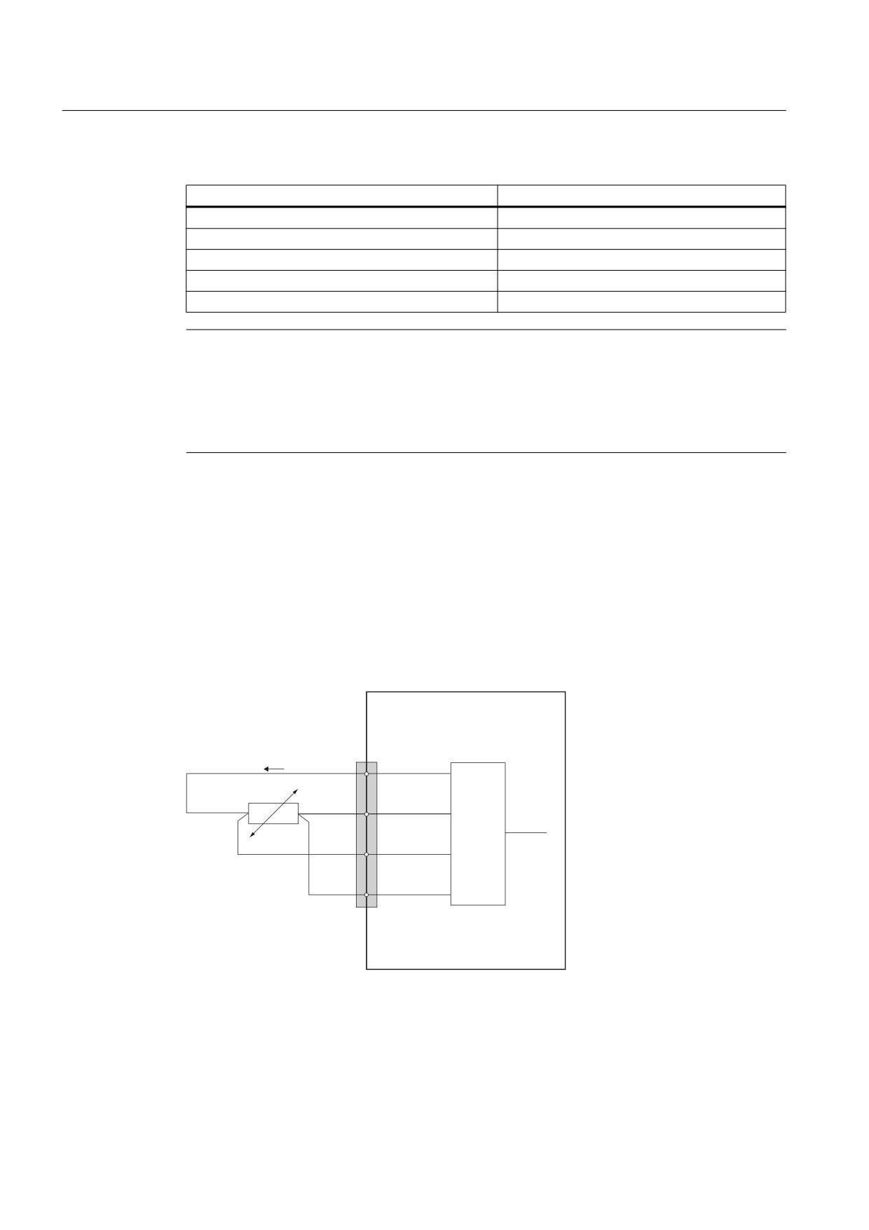
Connectable components
9.3 PP 72/48D 2/2A PN
Table 9-50
Technical data in the "PT100" operating mode
Parameter
Value
Input range (rated value)
- 200 ℃ to + 259 ℃
Standard
EN60751
Resolution
16 bits (including sign)
Accuracy
+/- 2 ℃
Internal resistance Ri
>> 10 kOhm
Note
If the PT100 operating mode is selected, the hardware is protected against overvoltage.
In the event of an error the following occurs:
1. An error bit is set which is then communicated to the PLC.
2. The module is shut down.
Measurement using a 4-wire connection system
Notes regarding the connection and operation of PT100 resistors:
This enables the module to supply X3 with a constant current via the CO1, CI1, CO2 and CI2
terminals. The constant current is fed to the resistor to be measured where it is then measured
as the voltage drop. It is imperative to wire the connected constant current cables directly to
the resistor.
Measurements with 4-wire connections compensate for line resistances and return a
considerably higher degree of precision in comparison with 2-wire connections.
33
'
$ 31
6LJQDO QDPH
,F
&2[
&,[
$'8
%XV
$,[
$,[
;
x
1, 2
ADU Analog Digital Unit
Ic
Constant current
Figure 9-19 PT100 pin assignment
NCU 7x0.3 PN, NCU 7x0.3B PN
132
Manual, 06/2014, 6FC5397-1EP40-5BA1

Connectable components
9.3 PP 72/48D 2/2A PN
Measurement using a 3-wire connection system
The following pins must be jumpered at connector X3 in order to perform the measurement in
the PT100 using a 3-wire connection system:
● Temperature measurement with channel 1:
Short-circuit pin 2 (CI 1) and pin 4 (AI 1-) and connect the jumper at connector X3
● Temperature measurement with channel 2:
Short-circuit pin 6 (CI 2) and pin 8 (AI 2-) and connect the jumper at connector X3.
Note
Measuring accuracy
The accuracy of the temperature input becomes poorer: The resistance of the connecting
cable of the jumpered connecting cable falsifies the measurement.
Analog outputs
The module has two analog outputs. These can optionally be assigned parameters as voltage
or current output.
Note
The analog outputs are only enabled following the parameter assignment.
From the switch-on of the I/O module to when it is enabled, the analog outputs do not read
0 V, but are defined by a voltage pulse at -0.2 V. This value must be taken into consideration
when specifying the setpoint value.
The cycle time of the analog value accumulation is limited by the PLC cycle.
Table 9-51
Technical specifications in the "voltage output" operating mode
Parameter
Value
Output range (rated value)
- 10 V to + 10 V
Permitted overrange
- 10.5 V to + 10.5 V
Resolution
16 bits (including sign)
Accuracy
+/- 0,5 %
Max. load current
-3 mA to +3 mA
Table 9-52
Technical specifications in the "current output" operating mode
Parameter
Value
Output range (rated value)
- 20 mA to + 20 mA
Permitted overrange
- 20.2 mA to + 20.2 mA
Resolution
16 bits (including sign)
Accuracy
+/- 0,5 %
Load impedance
≤ 600 ohm
NCU 7x0.3 PN, NCU 7x0.3B PN
Manual, 06/2014, 6FC5397-1EP40-5BA1
133
Connectable components
9.3 PP 72/48D 2/2A PN
9.3.5
Parameter assignment
9.3.5.1
Input / output images
Input image
The image comprises 3 slots (n, m, d ≙ start address):
● Slot 1: Digital inputs (DI)
- n+0 … n+8 (9 byte)
- X222.P3 - .P10 are rapid inputs
● Slot 2: 2 analog inputs (AI): m+0 … m+7 (8 byte)
● Slot 3: Diagnostics: d+0 .. d+1
Table 9-53
Input image of digital inputs for the 1st I/O module (n=0)
Terminal
Byte
Bit7
Bit6
Bit5
Bit4
Bit3
Bit2
Bit1
Bit0
n+0
Pin10
Pin9
Pin8
Pin7
Pin6
Pin5
Pin4
Pin3
DI 0.7
DI 0.6
DI 0.5
DI 0.4
DI 0.3
DI 0.2
DI 0.1
DI 0.0
X111
n+1
Pin18
Pin17
Pin16
Pin15
Pin14
Pin13
Pin12
Pin11
DI 1.7
DI 1.6
DI 1.5
DI 1.4
DI 1.3
DI 1.2
DI 1.1
DI 1.0
n+2
Pin26
Pin25
Pin24
Pin23
Pin22
Pin21
Pin20
Pin19
DI 2.7
DI 2.6
DI 2.5
DI 2.4
DI 2.3
DI 2.2
DI 2.1
DI 2.0
n+3
Pin10
Pin9
Pin8
Pin7
Pin6
Pin5
Pin4
Pin3
DI 3.7
DI 3.6
DI 3.5
DI 3.4
DI 3.3
DI 3.2
DI 3.1
DI 3.0
X222
n+4
Pin18
Pin17
Pin16
Pin15
Pin14
Pin13
Pin12
Pin11
DI 4.7
DI 4.6
DI 4.5
DI 4.4
DI 4.3
DI 4.2
DI 4.1
DI 4.0
n+5
Pin26
Pin25
Pin24
Pin23
Pin22
Pin21
Pin20
Pin19
DI 5.7
DI 5.6
DI 5.5
DI 5.4
DI 5.3
DI 5.2
DI 5.1
DI 5.0
n+6
Pin10
Pin9
Pin8
Pin7
Pin6
Pin5
Pin4
Pin3
DI 6.7
DI 6.6
DI 6.5
DI 6.4
DI 6.3
DI 6.2
DI 6.1
DI 6.0
X333
n+7
Pin18
Pin17
Pin16
Pin15
Pin14
Pin13
Pin12
Pin11
DI 7.7
DI 7.6
DI 7.5
DI 7.4
DI 7.3
DI 7.2
DI 7.1
DI 7.0
n+8
Pin26
Pin25
Pin24
Pin23
Pin22
Pin21
Pin20
Pin19
DI 8.7
DI 8.6
DI 8.5
DI 8.4
DI 8.3
DI 8.2
DI 8.1
DI 8.0
Table 9-54
Input image of analog inputs for the 1st I/O module (m=56)
Byte
Bit7
Bit6
Bit5
Bit4
Bit3
Bit3
Bit1
Bit0
m+0
Analog Status Byte 0
m+1
Analog Status Byte 1
m+2
Analog Status Byte 2
m+3
Analog Status Byte 3
m+4
AI 0.15
AI 0.14
AI 0.13
AI 0.12
AI 0.11
AI 0.10
AI 0.9
AI 0.8
m+5
AI 0.7
AI 0.6
AI 0.5
AI 0.4
AI 0.3
AI 0.2
AI 0.1
AI 0.0
NCU 7x0.3 PN, NCU 7x0.3B PN
134
Manual, 06/2014, 6FC5397-1EP40-5BA1
Connectable components
9.3 PP 72/48D 2/2A PN
Byte
Bit7
Bit6
Bit5
Bit4
Bit3
Bit3
Bit1
Bit0
m+6
AI 1.15
AI 1.14
AI 1.13
AI 1.12
AI 1.11
AI 1.10
AI 1.9
AI 1.8
m+7
AI 1.7
AI 1.6
AI 1.5
AI 1.4
AI 1.3
AI 1.2
AI 1.1
AI 1.0
Output image
The image comprises 2 slots (n, m, ≙ start address):
● Slot 1: Digital outputs (DO): n+0 … n+5 (6 byte)
● Slot 2: 2 analog outputs (AO): m+0 … m+7 (8 byte)
Table 9-55
Output image of digital outputs for the 1st I/O module (n=0)
Terminal
Byte
Bit7
Bit6
Bit5
Bit4
Bit3
Bit2
Bit1
Bit0
n+0
Pin38
Pin37
Pin36
Pin35
Pin34
Pin33
Pin32
Pin31
DO 0.7
DO 0.6
DO 0.5
DO 0.4
DO 0.3
DO 0.2
DO 0.1
DO 0.0
X111
n+1
Pin46
Pin45
Pin44
Pin43
Pin42
Pin41
Pin40
Pin39
DO 1.7
DO 1.6
DO 1.5
DO 1.4
DO 1.3
DO 1.2
DO 1.1
DO 1.0
n+2
Pin38
Pin37
Pin36
Pin35
Pin34
Pin33
Pin32
Pin31
DO 2.7
DO 2.6
DO 2.5
DO 2.4
DO 2.3
DO 2.2
DO 2.1
DO 2.0
X222
n+3
Pin46
Pin45
Pin44
Pin43
Pin42
Pin41
Pin40
Pin39
DO 3.7
DO 3.6
DO 3.5
DO 3.4
DO 3.3
DO 3.2
DO 3.1
DO 3.0
n+4
Pin38
Pin37
Pin36
Pin35
Pin34
Pin33
Pin32
Pin31
DO 4.7
DO 4.6
DO 4.5
DO 4.4
DO 4.3
DO 4.2
DO 4.1
DO 4.0
X333
n+5
Pin46
Pin45
Pin44
Pin43
Pin42
Pin41
Pin40
Pin39
DO 5.7
DO 5.6
DO 5.5
DO 5.4
DO 5.3
DO 5.2
DO 5.1
DO 5.0
Table 9-56
Output image of analog outputs for the 1st I/O module (m=56)
Byte
Bit7
Bit6
Bit5
Bit4
Bit3
Bit3
Bit1
Bit0
m+0
Analog Control Byte 0
m+1
Analog Control Byte 1
m+2
Analog Control Byte 2
m+3
Analog Control Byte 3
m+4
AO 0.15
AO 0.14
AO 0.13
AO 0.12
AO 0.11
AO 0.10
AO 0.9
AO 0.8
m+5
AO 0.7
AO 0.6
AO 0.5
AO 0.4
AO 0.3
AO 0.2
AO 0.1
AO 0.0
m+6
AO 1.15
AO 1.14
AO 1.13
AO 1.12
AO 1.11
AO 1.10
AO 1.9
AO 1.8
m+7
AO 1.7
AO 1.6
AO 1.5
AO 1.4
AO 1.3
AO 1.2
AO 1.1
AO 1.0
NCU 7x0.3 PN, NCU 7x0.3B PN
Manual, 06/2014, 6FC5397-1EP40-5BA1
135
Connectable components
9.3 PP 72/48D 2/2A PN
9.3.5.2
Assigning parameters to the analog inputs / outputs
Operating mode
Parameters are assigned to the operating mode via the m+0 byte (Analog Control Byte 0) of
the output image of the analog outputs:
Byte
Bit7
Bit6
Bit5
Bit4
Bit3
Bit3
Bit1
Bit0
m+0
AO
AO
AO
AO
AI
AI
AI
AI
(channel
(channel
(channel
(channel
(channel
(channel
(channel
(channel
4)
4)
3)
3)
2)
2)
1)
1)
m+1
Reserved
Data
format
m+2
Reserved
m+3
Reserved
The reserved bits must be preassigned with the value "0".
The operating mode is set to "no operating mode" during power-up, as soon as a valid setting
is made this will be applied and will subsequently no longer be reset. If a reset is initiated by
the user, this is interpreted as an error.
Type of control
The control type must be specified in the Analog Control Byte m+1 (bit 0), so that the 16 bit
input and output values from and for the analog module are correctly interpreted by the control.
In the SINUMERIK 840D sl control, the value "1" must be entered here.
Note
The control type must be set prior to the operating mode so that the first set of user data is
not misinterpreted. In addition to this, the Analog Control Byte m+0 / m+1 must only be
accessed byte by byte.
Assigning parameters to the analog inputs
The analog inputs (AI) can be operated in the following operating modes:
Operating mode 1st channel
Bit 1
Bit 0
No operating mode
0
0
Voltage measurement
0
1
Current measurement
1
0
Temperature measurement (Pt100)
1
1
Operating mode 2nd channel
Bit 3
Bit 2
No operating mode
0
0
Voltage measurement
0
1
NCU 7x0.3 PN, NCU 7x0.3B PN
136
Manual, 06/2014, 6FC5397-1EP40-5BA1
Connectable components
9.3 PP 72/48D 2/2A PN
Operating mode 2nd channel
Bit 3
Bit 2
Current measurement
1
0
Temperature measurement (Pt100)
1
1
Assigning parameters to the analog outputs
The analog outputs (AO) can be operated in the following operating modes:
Operating mode 3rd channel
Bit 5
Bit 4
No operating mode
0
0
Voltage output
0
1
Current output
1
0
Impermissible operating mode
1
1
Operating mode 4th channel
Bit 7
Bit 6
No operating mode
0
0
Voltage output
0
1
Current output
1
0
Impermissible operating mode
1
1
Checkback signal of the operating modes
The set operating modes are saved in the input image in Status Byte 0. This value must be
compared with Control Byte 0 in the output image. If these are different, an error has occurred,
e. g. in the case of overvoltage in the "Temperature measurement" operating mode, see
Diagnostics via input image (Page 142).
NCU 7x0.3 PN, NCU 7x0.3B PN
Manual, 06/2014, 6FC5397-1EP40-5BA1
137
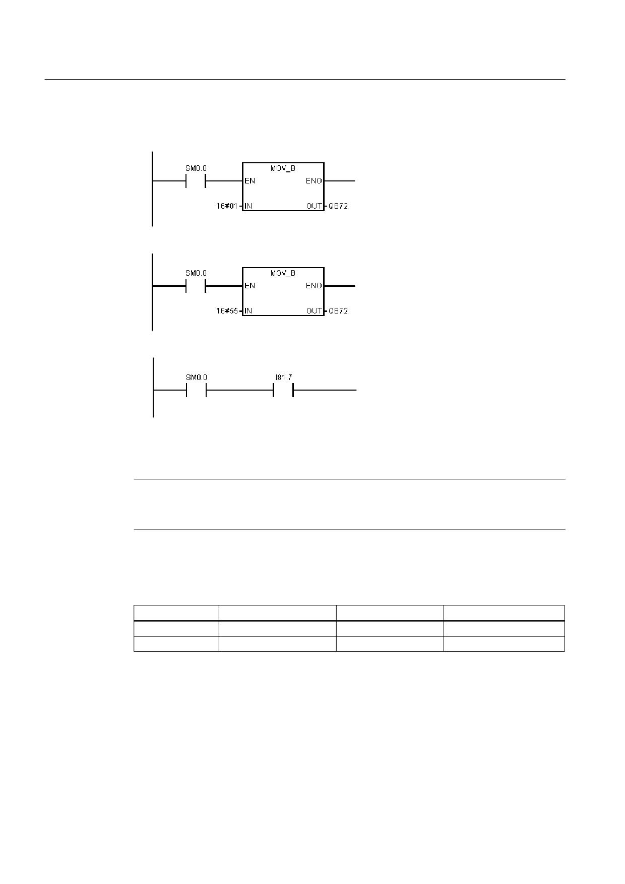
Connectable components
9.3 PP 72/48D 2/2A PN
Examples of programming
1. Determine control type:
2. Set the operating mode:
3. Query the error status bit in cyclic operation:
9.3.5.3
Analog value representation
Note
The analog values of the inputs and outputs are written or read in 16 bit data format i.e. they
must be accessed word by word.
The analog values are provided as 16 bit integer values. Depending on the operating mode,
the measured values must be converted using the following factors in order to achieve the
corresponding physical value.
Voltage [V]
Current [mA]
Temperature [°C]
Factor (AI):
0.00152
0.00305
0.1
Factor (AO):
0.00038
0.00076
-
Calculation: 16 bit value (hex. or dec.) * factor = measured value
NCU 7x0.3 PN, NCU 7x0.3B PN
138
Manual, 06/2014, 6FC5397-1EP40-5BA1
Connectable components
9.3 PP 72/48D 2/2A PN
Analog inputs
Table 9-57
Measured values in the voltage measurement operating mode
16 bit value (hex.)
16 bit value (dec.)
Factor
Voltage value [V]
Overflow
-
Deactivation
Overrange
-
Up to 11.75 V
0x19B5
6581
10 V
0x0CDA
3291
5 V
0x066D
1645
2.5 V
0x0000
0
0.00152
0 V
0xF993
-1645
-2.5 V
0xF326
-3291
-5 V
0xE64B
-6581
-10 V
Underrange
-
Up to -11.75 V
Underflow
-
Deactivation
Table 9-58
Measured values in the current measurement operating mode
16 bit value (hex.)
16 bit value (dec.)
Factor
Current value [V]
Overflow
-
Deactivation
Overrange
-
Up to 23.5 mA
0x1999
6553
20 mA
0x0CCC
3277
10 mA
0x0000
0
0.00305
0 mA
0xF333
-3277
-10 mA
0xE666
-6553
-20 mA
Underrange
-
Up to -23.5 mA
Underflow
-
Deactivation
Table 9-59
Measured values in the "temperature measurement" operating mode
16 bit value (hex.)
16 bit value (dec.)
Factor
Temperature value [V]
Overflow
0x0A28
2590
259 ℃
0x03E8
1000
100 °C
0x01F4
500
50 ℃
0x0000
0.0
0.1
0 °C
0xFE0C
-500
-50 ℃
0xFC18
-1000
-100 °C
0xF830
-2000
-200 ℃
Underflow
NCU 7x0.3 PN, NCU 7x0.3B PN
Manual, 06/2014, 6FC5397-1EP40-5BA1
139
Connectable components
9.3 PP 72/48D 2/2A PN
Note
If a Pt100 element is accidentally not connected in this operating mode and an input voltage
higher than 0.25 V is output, the analog module automatically switches to the "no operating
mode" operating mode and resets the gain factor to "1". This is signalized in Status Word 0
(channel-specific) in the input image. In addition, a corresponding error code is output in the
diagnostics slot at a counter value of "2".
In the case of operation without a Pt100 element, a slightly negative voltage may be applied,
which results in an error status for the module. Here, the "PNFault" LED and the status byte
1 are to be observed.
Analog outputs
Table 9-60
Measured values in the "voltage output" operating mode
16 bit value (hex.)
16 bit value (dec.)
Factor
Voltage value [V]
Overflow
-
Deactivation
Overrange
-
Up to 10.5 V
0x6666
26214
10 V
0x4CD1
19665
7.5 V
0x199B
6555
2.5 V
0x0000
0
0.00038
0 V
0xE665
-6555
-2.5 V
0xB32F
-19665
-7.5 V
0x999A
-26214
-10 V
Underrange
-
Up to -10.5 V
Underflow
-
Deactivation
Table 9-61
Measured values in the "current output" operating mode
16 bit value (hex.)
16 bit value (dec.)
Factor
Current value [V]
Overflow
-
Deactivation
Overrange
-
20.2 mA
0x6666
26214
20 mA
0x4CD1
19665
15 mA
0x199B
6555
5 mA
0x0000
0
0.00076
0 mA
0xE665
-6555
-5 mA
0xB32F
-19665
-15 mA
0x999A
-26214
-20 mA
Underrange
-
-20.2 mA
Underflow
-
Deactivation
NCU 7x0.3 PN, NCU 7x0.3B PN
140
Manual, 06/2014, 6FC5397-1EP40-5BA1
Connectable components
9.3 PP 72/48D 2/2A PN
9.3.5.4
Examples
The following examples for assigning parameters to analog inputs / outputs are provided for
the I/O module with device number "7".
Table 9-62
Measured values and responses in the voltage measurement operating mode
Address
Voltage ±10 V
0 V
2.5 V
10 V
12 V
Operating mode
QB72
16#55
16#55
16#55
16#55
Format
QB73
16#1
16#1
16#1
16#1
Value
QW76
16#0
16#199B
16#6666
16#7AE1
Value
QW78
16#0
16#199B
16#6666
16#7AE1
Operating mode
IB72
16#55
16#55
16#55
16#55
Format
IB73
16#1
16#1
16#1
16#1
Value
IW76
16#0
16#66D
16#19B5
16#0
Value
IW78
16#0
16#66D
16#19B5
16#0
Diagnostics
IB50
-
-
-
16#2
IB51
16#0
16#0
16#0
16#7
PNFault LED
off
off
off
on
Troubleshooting
Deactivating/
activating
Table 9-63
Measured values and responses in the current measurement operating mode
Address
Current 20 mA
0 mA
5 mA
20 mA
22 mA
Operating mode
QB72
16#AA
16#AA
16#AA
16#AA
Format
QB73
16#1
16#1
16#1
16#1
Value
QW76
16#0
16#199B
16#6666
16#70A5
Value
QW78
16#0
16#199B
16#6666
16#70A5
Operating mode
IB72
16#AA
16#AA
16#AA
16#AA
Format
IB73
16#1
16#1
16#1
16#81
Value
IW76
16#0
16#665
16#1996
16#0
Value
IW78
16#0
16#665
16#1996
16#0
Diagnostics
IB50
-
-
-
16#2
IB51
16#0
16#0
16#0
16#7
PNFault LED
off
off
off
on
Troubleshooting
Deactivating/
activating
NCU 7x0.3 PN, NCU 7x0.3B PN
Manual, 06/2014, 6FC5397-1EP40-5BA1
141
Connectable components
9.3 PP 72/48D 2/2A PN
Table 9-64
Measured values and responses in the temperature measurement operating mode
Address
Pt100
Incorrect operating mode
Resistor is not connected
Operating mode
QB72
16#AA
16#0F
Format
QB73
16#1
16#1
Value
QW76
-
-
Value
QW78
-
-
Operating mode
IB72
16#AA
16#0F
Format
IB73
16#81
16#81
Value
IW76
-
-
Value
IW78
-
-
Diagnostics
IB50
16#2
16#2
IB51
16#3
16#6
PNFault LED
on
on
Troubleshooting
Deactivating/activating
Deactivating/activating
9.3.5.5
Diagnostics via input image
Table 9-65
Diagnostics input image
Byte
Bit7
Bit6
Bit5
Bit4
Bit3
Bit3
Bit1
Bit0
d+0
count_2
count_1
count_0
T_Alarm_2
T_Alarm_1
Diag_2
Diag_1
Diag_0
d+1
Status_1
Table 9-66
Messages in byte 0
Bit
Signal name
Message
7
count_2
alive and well 2
6
count_1
alive and well 1
5
count_0
alive and well 0
4
T_Alarm_2
Temperature not within the operating temperature range defined for the
module
3
T_Alarm_1
Critical temperature exceeded
2
Diag_2
Overload DO byte 5/4
1
Diag_1
Overload DO byte 3/2
0
Diag_0
Overload DO byte 1/0
NCU 7x0.3 PN, NCU 7x0.3B PN
142
Manual, 06/2014, 6FC5397-1EP40-5BA1
Connectable components
9.3 PP 72/48D 2/2A PN
Note
The "alive and well" counter is a 3 bit modulo counter at the PP application level. The PP
application can be monitored using this counter. Failure of the application software does not
generally result in a communication failure, as this is developed in a hardware-supported
manner. The watch dog switches off the digital outputs, while the inputs remain at their last
set values.
Table 9-67
Overview of the messages in byte 1, depending on the "alive and well" counter
"alive and
Value
Message
well" counter
byte 1
0
0
Reserved
1
Temperature value
2
0
No error
1
Impermissible input voltage in the temperature measurement mode
2
Reserved
3
Overload at the outputs
4
Incorrect operating mode selection
5
Internal error, system error
6
Range exceeded at the inputs
7
Range exceeded at the outputs
3 ... 7
0
Reserved
Table 9-68
Elimination of error for "alive and well" counter status "2"
Value
Cause
Effect
Remedy
byte 1
1
In the temperature
The "PNFault" LED is activated.
It is essential that a Pt100 element is
measurement operating
connected to terminals 3.4 or 7.8.
The outputs are disabled. 1)
mode, an input voltage is too
The module must be restarted with
The value 0x80 is stored in status byte 1.
high. The hardware may
Power ON after the error has been
become damaged/
eliminated.
destroyed as a result.
2
Reserved
-
-
3
Overload at the outputs
The "PNFault" LED is activated.
Check the loads at the analog output.
The outputs are disabled. 1)
The module must be restarted with
Power ON after the error has been
The value 0x80 is stored in status byte 1.
eliminated.
4
Incorrect operating mode
Selection of operating mode is rejected,
If selected correctly, the module switches
selection, e.g. temperature
to cyclic operation.
measurement at the analog
outputs.
5
Internal error, system error
The "PNFault" LED is activated.
The firmware has detected a system
error, this status can only be exited by
The outputs are disabled. 1)
means of a switch-on / switch-off.
The value 0x80 is stored in status byte 1.
NCU 7x0.3 PN, NCU 7x0.3B PN
Manual, 06/2014, 6FC5397-1EP40-5BA1
143
Connectable components
9.3 PP 72/48D 2/2A PN
Value
Cause
Effect
Remedy
byte 1
6
Range exceeded at the
Check input circuit and adjust, if required.
inputs
7
Range exceeded at the
Correct the values in the user program.
outputs
1)
The analog outputs retain their last specified value.
Diagnostics via status bytes 0/1
In status byte 0, the set operating modes are reflected e.g. "0x55" if control byte 0 = 0x55 has
been specified (voltage on all channels).
In the event of an error, the error bit is set in status byte 1 (bit 7). In the event of an error in
one channel, all channels are deactivated.
Table 9-69
Input image of analog inputs (excerpt)
Byte
Bit7
Bit6
Bit5
Bit4
Bit3
Bit3
Bit1
Bit0
m+0
0
0
0
0
0
0
0
0
m+1
Error bit
0
0
0
0
0
0
0
9.3.6
Technical data
Table 9-70
Technical data of the I/O module
Safety
Degree of protection
IP 00 according to EN 60529
Protection class
III; DVC A, (PELV) acc. to EN 61800-5-1
Approvals
cULus, CE
Electrical data
Rated voltage
24 V DC
Rated current
0.7 A
Power consumption at rated load
19 W (without digital outputs)
Power loss
18 W
Mechanical data
Dimensions WxHxD
150 x 300 x 35 mm
Weight, approx.
0.9 kg
For detailed technical data relating to the inputs and outputs, see the "Connecting" chapter.
X111, X222 and X333 digital inputs/outputs (Page 124)
Analog X3 inputs/outputs (Page 130)
NCU 7x0.3 PN, NCU 7x0.3B PN
144
Manual, 06/2014, 6FC5397-1EP40-5BA1
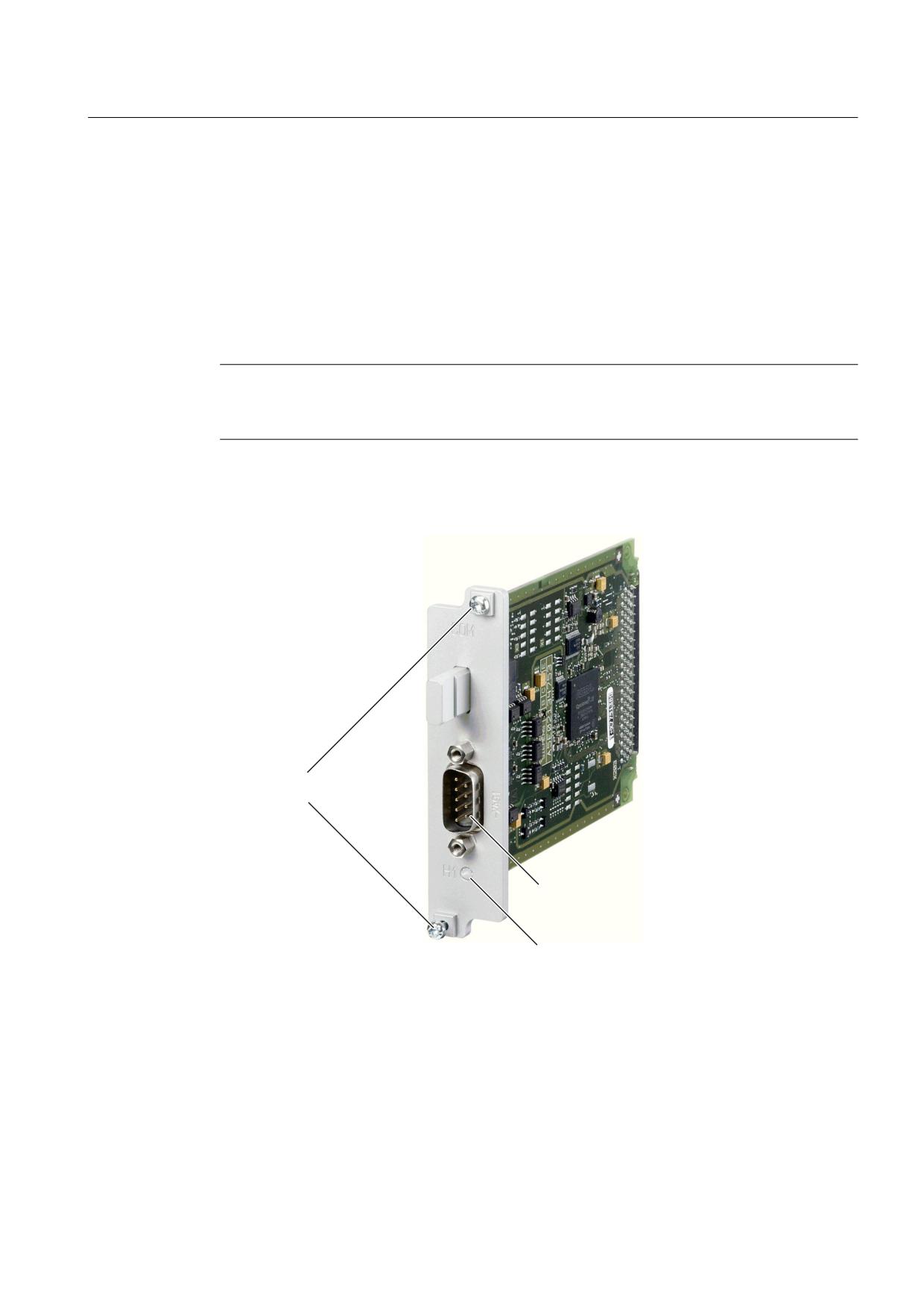
Connectable components
9.4 COM01.3 RS 232C (V.24) module
9.4
COM01.3 RS 232C (V.24) module
9.4.1
Description
The COM01.3 RS 232C (V. 24) option board can be inserted into the option slot of the NCU.
An NCU can be connected to a master computer or modem via COM port X491. The COM
port has been designed in accordance with the "ANSI/EIA/TIA-232-F-1997" standard.
Note
The option board COM01.3 RS 232C (V.24) module cannot be used for the NCU730.3B PN
with PLC 319 DP/PN.
Illustration
5HWDLQLQJ VFUHZV
&20 SRUW ;
2SHUDWLQJ VWDWH /(' +
Figure 9-20 COM01.3 RS 232C (V.24) module
NCU 7x0.3 PN, NCU 7x0.3B PN
Manual, 06/2014, 6FC5397-1EP40-5BA1
145
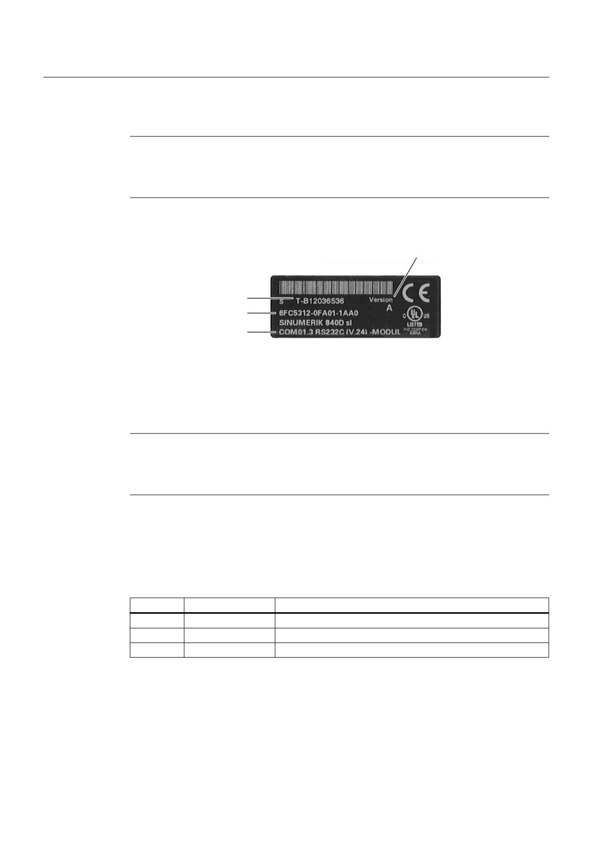
Connectable components
9.4 COM01.3 RS 232C (V.24) module
Type plate
Note
You might need to access the information provided on the type plate after mounting. Since
the type plates after mounting the option board can no longer be read, we recommend that
you at least note down the serial number before mounting.
The following diagram shows you all of the information provided on the type plate.
+: YHUVLRQ
6HULDO QXPEHU
2UGHU QXPEHU
&RPSRQHQW QDPH
Figure 9-21 COM01.3 RS 232C (V.24) module type plate
This plate is only visible, when the option board has been removed; it is attached to the
underside of the option board.
Note
The contents of the individual type plate fields on the actual option board may differ from
those described in this manual (e.g. updated product status, approvals and markings not yet
issued, etc.).
LED displays
LED H1 is located under the COM port. This can display the following operating states:
Table 9-71
LED displays, H1
Color
Status
Meaning
Orange
lit
COM01.3 is ready; after reset.
Green
lit
COM01.3 is active.
Red
lit
Operating error
NCU 7x0.3 PN, NCU 7x0.3B PN
146
Manual, 06/2014, 6FC5397-1EP40-5BA1
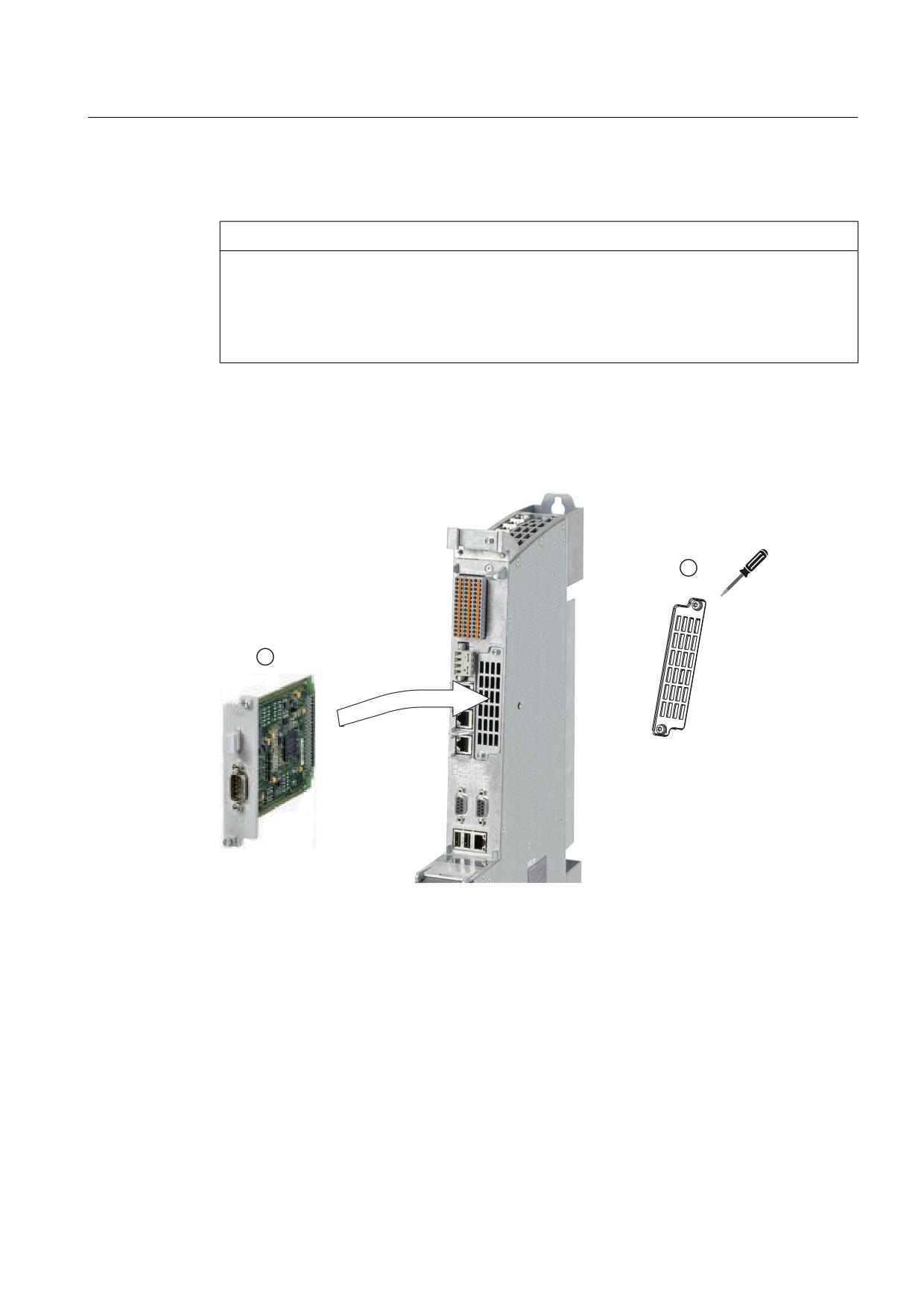
Connectable components
9.4 COM01.3 RS 232C (V.24) module
9.4.2
Installation/Mounting
NOTICE
Damage to the option board by inserting and withdrawing in operation
● Option boards should only be inserted and removed when the NCU and option board are
in a no-current condition.
● Option boards may only be operated by qualified personnel. The ESD notices must be
observed.
Installing the COM01.3 RS 232C (V.24) module
A COM01.3 option board is installed in the option slot of the NCU.
① Release the M3 fixing screws and remove the protective cover.
② Insert and secure the option board.
Tightening torque of the M3 fixing screws: 0.8 Nm.
Figure 9-22 Installing COM01.3
The cable outlet is at the top.
9.4.3
Connection
The RS 232C (V.24) module has a standardized serial interface.
NCU 7x0.3 PN, NCU 7x0.3B PN
Manual, 06/2014, 6FC5397-1EP40-5BA1
147