HV610C Series Frequency Inverter. User Manual (Version: 3.1.14) - page 6
Section VI. Fault Diagnosis & Solutions
Section VI. Fault Diagnosis & Solutions
HV610C is able to make full use of the device performance, while implementing effective
protection. You may encounter following fault tips during operation, please control the following
table analysis the possible causes, and rule out the fault.
6.1
Fault alarm and solutions
HV610C series can not only make full use of equipment performance but also implement
effective protection. HV610C series has 51 alarming information and protection function.Once
fault occurs, protection function acts,output stops, inverter fault relay contact starts,and fault
code is been displayed on the display panel. Before consulting the service department, the user
can perform self-check according to the prompts of this chapter, analyze the fault cause and find
out t solution. If the fault is caused by the reasons as described in the
dotted frame, please
consult the agents or our company directly.
Among the 51 items of warning information:
Fault no.22= Err22 refers to hardware over-current or over-voltage
signal.In
most cases
hardware over-voltage fault led to fault no.22= Err22 alarming.
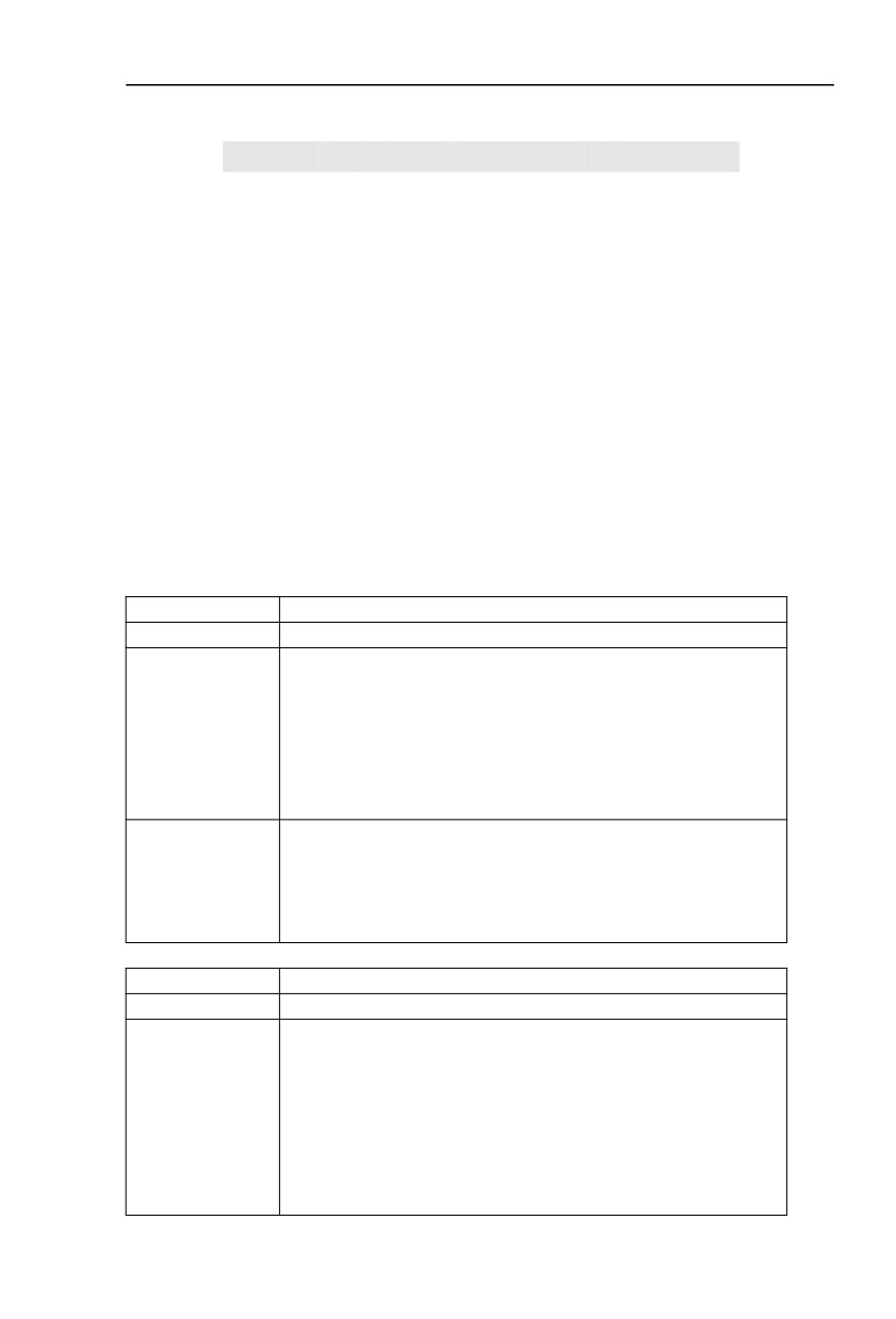
Fault name
Inverter unit protection
Panel display
Fault No.1= Err01
1、Inverter output loop short circuit
2、Two long wiring between motor and inverter.
3、Module overheating
Fault investigation
4、Inverter internal wiring loose
5、Main control board anomalies
6、Drive board anomalies
7、Inverter module anomalies
1、Eliminate external faults
2、Add reactor or output filter
Fault
3、Check air duct, fan and eliminate existing problems.
countermeasures
4、Insert all connecting wires
5、For technical support
Fault name
Acceleration over current
Panel display
Fault No.2= Err02
1、Acceleration time too short
2、Improper manual torque boost or V/F curve
3、Low voltage
4、Inverter output loop grouded or short circuit
Fault investigation
5、Vector control mode without parameter identification
6、Start the rotating motor
7、Sudden load add in acceleration process
8、Small type selection of inverter.
115
Section VI. Fault Diagnosis & Solutions
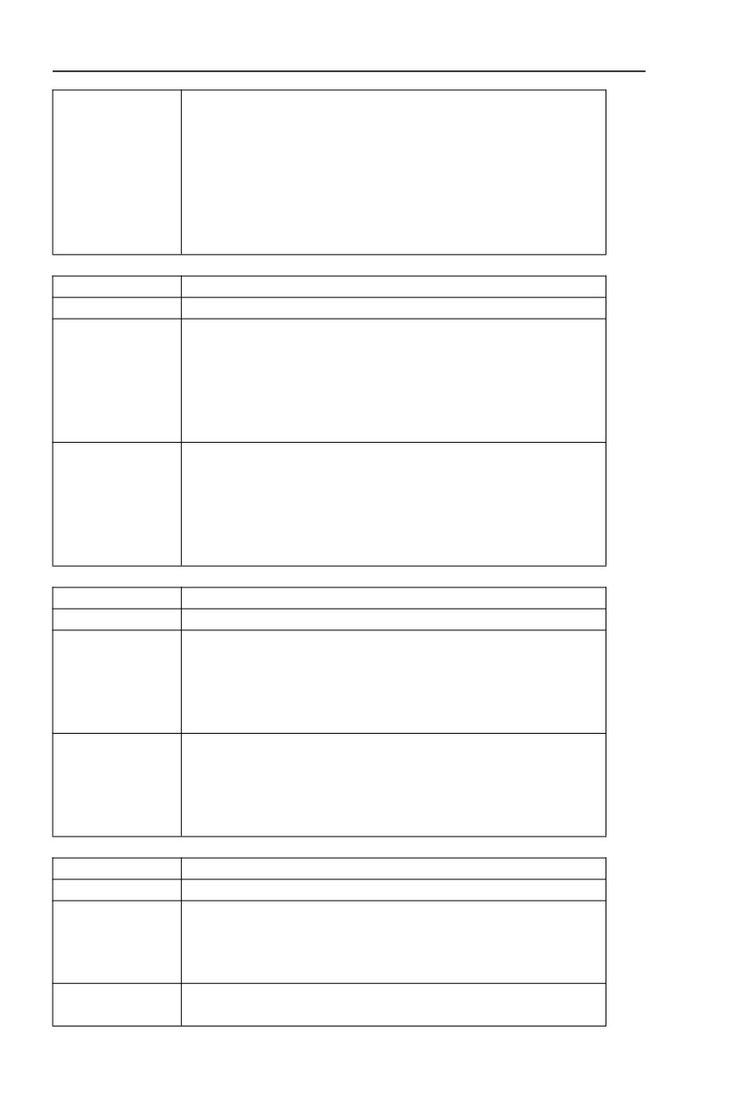
1、Increase acceleration time
2、Adjust manual torque boost or V/F curve
3、Adjust voltage to normal range
Fault
4、Eliminate external faults
countermeasures
5、Parameter identification
6、Select speed tracking start or restart after motor stop
7、Cancel sudden added load
8、Choose inverter of greater power level
Fault name
Deceleration over current
Panel display
Fault No.3= Err03
1、Inverter output loop grouded or short circuit
2、Vector control mode without parameter identification
3、Deceleration time too short
Fault investigation
4、Low voltage
5、Sudden load add in deceleration process
6、No braking unit and brake resistence installed
1、Eliminate external faults
2、Parameter identification
Fault
3、Increase deceleration time
countermeasures
4、Adjust voltage to normal range
5、Cancel sudden added load
6、Install braking unit and brake resistence
Fault name
Constant speed over current
Panel display
Fault No.4= Err04
1、Inverter output loop grouded or short circuit
2、Vector control mode without parameter identification
Fault investigation
3、Low voltage
4、Sudden load add in deceleration process
5、Small type selection of inverter
1、Eliminate external faults
2、Parameter identification
Fault
3、Adjust voltage to normal range
countermeasures
4、Cancel sudden added load
5、Choose inverter of greater power level
Fault name
Acceleration over voltage
Panel display
Fault No.5= Err05
1、No braking unit and brake resistence installed
2、High input voltage
Fault investigation
3、External force drive motor operation during acceleration process
4、Acceleration time too short
Fault
1、Install braking unit and brake resistence
countermeasures
2、Adjust voltage to normal range
116
Section VI. Fault Diagnosis & Solutions
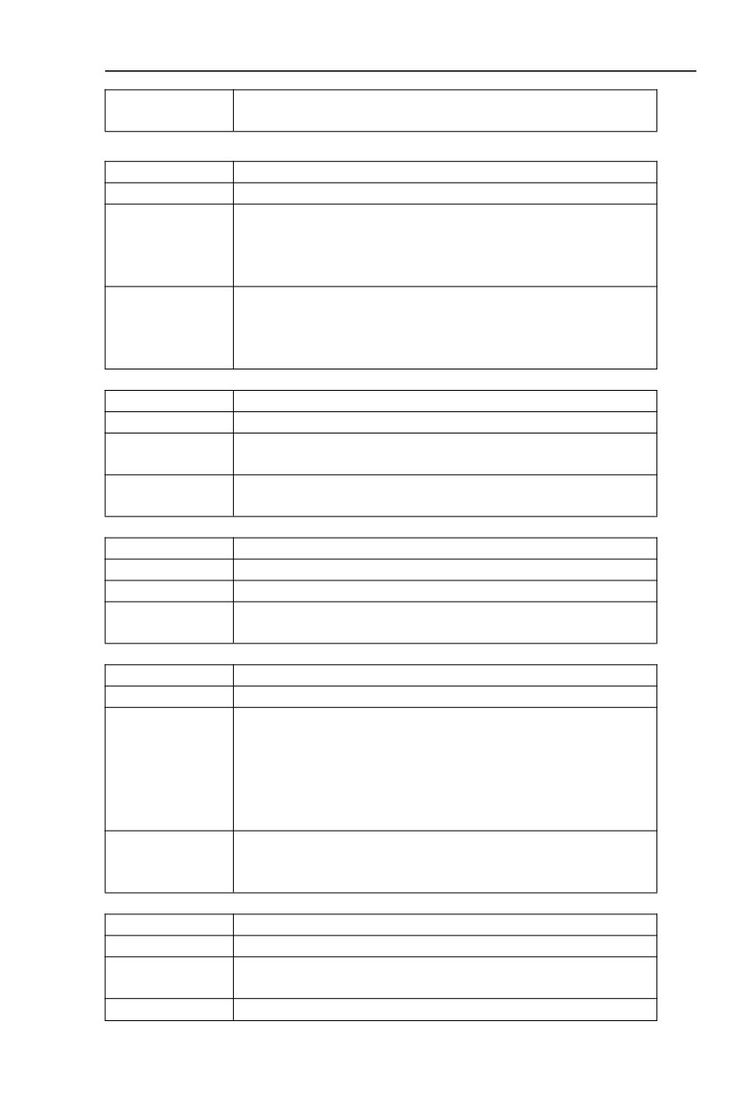
3、Cancel external force or install brake resistence
4、Increase acceleration time
Fault name
Deceleration over voltage
Panel display
Fault No.6= Err06
1、High input voltage
2、External force drive motor operation during deceleration process
Fault investigation
3、Deceleration time too short
4、No braking unit and brake resistence installed
1、Adjust voltage to normal range
Fault
2、Cancel external force or install brake resistence
countermeasures
3、Increase deceleration time
4、Install braking unit and brake resistence
Fault name
Constant speed over voltage
Panel display
Fault No.7= Err07
1、External force drive motor operation
Fault investigation
2、High input voltage
Fault
1、Cancel external force or install brake resistence
countermeasures
2、Adjust voltage to normal range
Fault name
Control power supply fault
Panel display
Fault No.8= Err08
Fault investigation
1、Input voltage is not within the specified range
Fault counter
1、Adjust voltage to normal range
measures
Fault name
Under-voltage fault
Panel display
Fault No.9= Err09
1、Instantaneous power-off
2、Input voltage is not within the specified range
3、Bus voltage anomalies
Fault investigation
4、Rectifier and buffer resistance anomalies
5、Drive board anomalies
6、Control board anomalies
1、Reset fault
Fault
2、Adjust voltage to normal range
countermeasures
3、For technical support
Fault name
Inverter overload
Panel display
Fault No.10= Err10
1、Small type selection of inverter.
Fault investigation
2、Overload or motor stall
Fault
1、Choose inverter of greater power level
117
Section VI. Fault Diagnosis & Solutions
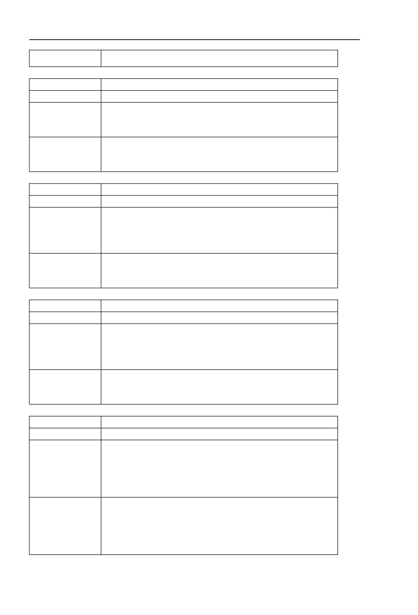
countermeasures
2、Reduce the load and check the motor and mechanical condition
Fault name
Motor overload
Panel display
Fault No.11= Err11
1、Small type selection of inverter
Fault investigation
2、Improper setup of F9.01
3、Overload or motor stall
1、Choose inverter of greater power level
Fault counter
2、Set F9.01 correctly
measures
3、Reduce the load and check the motor and mechanical condition
Fault name
Input phase lack
Panel display
Fault No.12= Err12
1、Drive board anomalies
2、Lightning protection board (BESP ) anomalies
Fault investigation
3、Control board anomalies
4、3-phase input power-supply anomalies
1、Replace driver, power- supply board or contactor
Fault
2、For technical support
countermeasures
3、Eliminate external loop faults
Fault name
Output phase lack
Panel display
Fault No.13= Err13
1、Wiring between motor and inverter anomalies
2、Inverter unbalanced 3-phase output
Fault investigation
3、Drive board anomalies
4、Module anomalies
1、Eliminate external loop faults
Fault counter
2、Check 3-phase winding and eliminate faults
measures
3、For technical support
Fault name
Module overheating
Panel display
Fault No.14= Err14
1、Air duct block
2、Fan damage
Fault investigation
3、High ambient temperature
4、Module thermistor damage
5、Inverter module damage
1、Clean air dust
2、Replace the fan
Fault counter
3、Reduce ambient temperature
measures
4、Replace thermistor
5、Replace inverter module
118
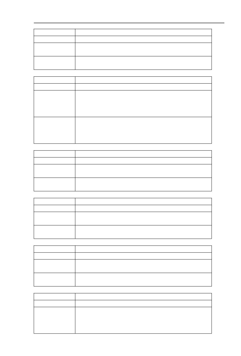
Section VI. Fault Diagnosis & Solutions
Fault name
External equipment fault
Panel display
Fault No.15= Err15
1、Input external fault signal through DI
Fault investigation
2、Input external fault signal through IO
Fault counter
1、Reset operation
measures
Fault name
Communication fault
Panel display
Fault No.16= Err16
1、Abnornal communication cable
2、Wrongly set communication expansion card F0.28
Fault investigation
3、Wrongly set communication parameter FD group
4、Position machine operation anomalies
1、Check the communication cable
Fault counter
2、Set communication expansion card type correctly
measures
3、Set communication parameter correctly
4、Check position machine cable
Fault name
Contactor fault
Panel display
Fault No.17= Err17
1、Input phase lack
Fault investigation
2、Drive board , contactor anomalies
Fault counter
1、Eliminate external loop faults
measures
2、Replace driver, power- supply board or contactor
Fault name
Current inspection fault
Panel display
Fault No.18= Err18
1、Drive board anomalies
Fault investigation
2、Hall devices anomalies
Fault counter
1、Replace drive board
measures
2、Replace hall devices
Fault name
Motor tuning fault
Panel display
Fault No.19= Err19
1、Parameter identification process overtime
Fault investigation
2、Wrongly set motor parameters
Fault counter
1、Check wire between inverter and motor
measures
2、Set motor parameters correctly according to the nameplate
Fault name
Encoder /PG card fault
Panel display
Fault No.20= Err20
1、Encoder anomalies
2、PG card anomalies
Fault investigation
3、Encoder type mismatch
4、Encoder connections fault
119
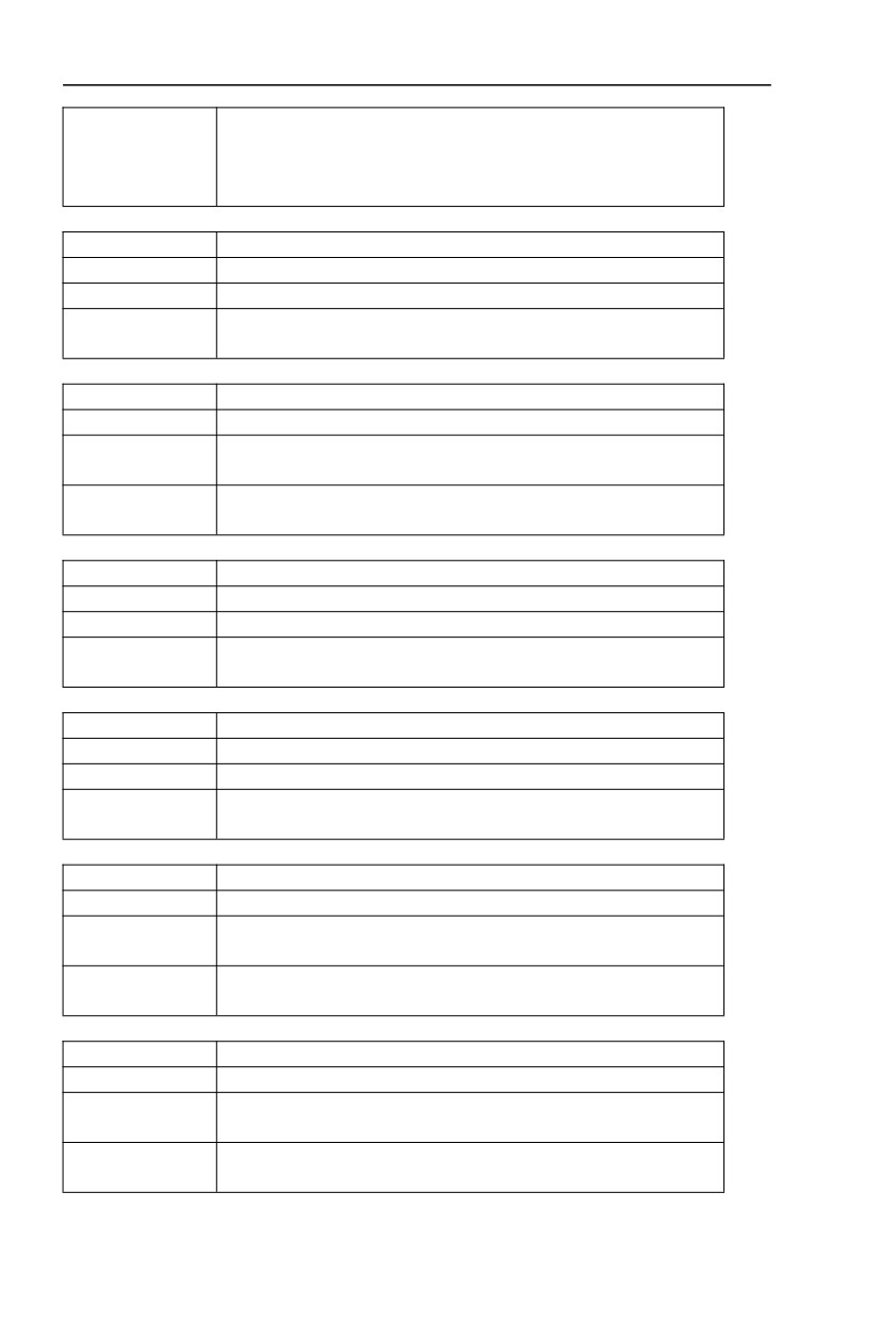
Section VI. Fault Diagnosis & Solutions
1、Replace encoder
Fault counter
2、Replace PG card
measures
3、Set motor encoder type correctly
4、Eliminate circuit faults
Fault name
EEPROM read & write fault
Panel display
Fault No.21= Err21
Fault investigation
1、EEPROM chip damage
Fault counter
1、Replace main control board
measures
Fault name
Inverter hardware fault
Panel display
Fault No.22= Err22
1、Presence of over-voltage
Fault investigation
2、Presence of over-current
Fault counter
1、Treat according to over voltage fault
measures
2、Treat according to over-current fault
Fault name
Short circuit to ground fault
Panel display
Fault No.23= Err23
Fault investigation
1、Motor short circuit to ground
Fault counter
1、Replace cable or motor
measures
Fault name
Total running time arrival fault
Panel display
Fault No.26= Err26
Fault investigation
1、Total running time arrive the set value
Fault counter
1、Clear record information using parameter initialization function
measures
Fault name
User-defined fault 1
Panel display
Fault No.27= Err27
1、Input user-defined fault 1 signal through multi-function terminal DI
Fault investigation
2、Input user-defined fault 1 signal through virtual IO function
Fault counter
1、Reset operation
measures
Fault name
User-defined fault 2
Panel display
Fault No.28= Err28
1、Input user-defined fault 2 signal through multi-function terminal DI
Fault investigation
2、Input user-defined fault 2 signal through virtual IO function
Fault counter
1、Reset operation
measures
120
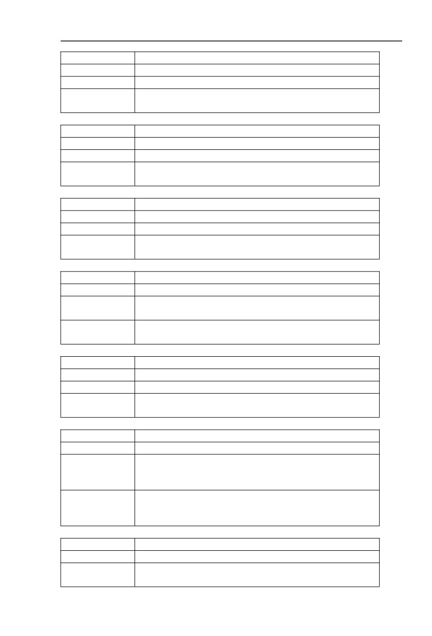
Section VI. Fault Diagnosis & Solutions
Fault name
Total power-on time arrival fault
Panel display
Fault No.29= Err29
Fault investigation
1、Total power-on time arrive the set value
Fault counter
1、Clear record information using parameter initialization function
measures
Fault name
Load off fault
Panel display
Fault No.30= Err30
Fault investigation
1、Inverter running current less than F9.64
Fault counter
1、Confirm whether load off or F9.64, F9.65parameter settings is
measures
inaccordance with the actual operating condition
Fault name
PID feedback loss during operation fault
Panel display
Fault No.31= Err31
Fault investigation
1、PID feedback less than FA.26 set value
Fault counter
1、Check PID feedback signal or set FA.26 to a proper value
measures
Fault name
Each wave current limiting fault
Panel display
Fault No.40= Err40
1、Excessive load or motor stall
Fault investigation
2、Small type selection of inverter.
Fault counter
1、Reduce the load and check the motor and mechanical condition
measures
2、Choose inverter of greater power level
Fault name
Motor switching fault
Panel display
Fault No.41= Err41
Fault investigation
1、Change current motor selection during inverter operation
Fault counter
1、Switch the motor after inverter stopped.
measures
Fault name
Excessive speed deviation fautl
Panel display
Fault No.42= Err42
1、Improper set inspection parameters F9.69、F9.60
Fault investigation
2、Wrongly set encoder parameters
3、No parameter identification
1、Set inspection parameters properly according to actual situation
Fault counter
2、Set motor encoder parameters correctly
measures
3、Motor parameter identification
Fault name
Motor overspeed fault
Panel display
Fault No.43= Err43
1、No parameter identification
Fault investigation
2、Wrongly set encoder parameters
121
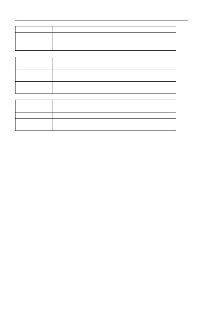
Section VI. Fault Diagnosis & Solutions
3、Improper set inspection parameters F9.69、F9.60
1、Motor parameter identification
Fault counter
2、Set motor encoder parameters correctly
measures
3、Set inspection parameters properly according to actual situation
Fault name
Motor overtemperature fault
Panel display
Fault No.45= Err45
1、Temperature sensor wiring loose
Fault investigation
2、Motor over-temperature
Fault counter
1、Check sensor wiring and eliminate fault
measures
2、Reduced carrier frequency or take other cooling measures for the motor
Fault name
Initial position fault
Panel display
Fault No.51= Err51
Fault investigation
1、Excessive deviation between motor parameters and the paractical value
Fault counter
1、Reconfirm motor parameter settings, pay attention to the rated current
measures
value
122
Section VII. Inspection & Maintenance
Section VII. Inspection & Maintenance
7.1 Inspection and Maintenance
Under normal working conditions, in addition to daily inspection, the frequency converter
should be subject to regular inspection (for example inspection for overhaul or as specified but
at an interval of at most six months). Please refer to the following table in order to prevent faults.
Daily
Regular
Check item
Check details
Method
Criterion
LED display
If any abnormal display
Visual check
As per use state
√
If any abnormal noise or
√
√
Fan
Visual and audible check
No anomalies
vibration
Surrounding
Temperature, humidity, dust
Visual\audible\sensory
√
As per 2-1 item
conditions
content, harmful gas, etc.
check
Input output
If any abnormal input, output
Measure R, S, T and
As per standard
√
voltage
voltage
U, V, W terminals
specifications
Fasteners whether loose, if
any signs showing overheat,
Check visually, tighten
Main circuit
discharging, or too high dust
the fastenings, and clean
No anomalies
√
content, or the air piping is
the related parts
blocked
Electrolytic
If any abnormal appearance
Check visually
No anomalies
√
capacitor
Current-conducting
√
Loose or not
Check visually
No anomalies
leads or blocks
Tighten the loose
Terminals
If the screws or bolts loose
No anomalies
√
screws or bolts
“√” means need daily check or regularly check.
For inspection,do not disassemble or shake the parts without reason, or pull off the plug-in-
parts at random. Otherwise, the unit will not operate normally, or can not enter the mode of fault
display, or causes faults of components or even parts of the main switch components IGBT
module is damaged.
When needing measurement, the user should note that much different results will be gained
possibly if the measuring is performed with different instruments. It is recommended that the
input voltage be measured with pointer-type voltmeter, output voltage with rectification voltmeter,
input and output current with tong-test ammeter, and power with electrically-driven watt-meter.
123
Section VII. Inspection & Maintenance
7.2 Regular replacement of the device
In order to ensure the operation reliability of the frequency converter, in addition to regular
maintenance and inspection, all the parts suffering long-term mechanical wear should be
replaced at a regular interval, which includes all cooling fans and the filtering capacitors of main
circuits for energy buffer and interchange and PCBs. For continuous use under normal
conditions, these parts can be replaced according to the following table and the operating
environment, loads and the current state of frequency converter.
Part name
Standard replacement years
Cooling fan
1~3 years
Filtering capacitor
4~5 years
PCB
5~8 years
(printed circuit board)
7.3 Storage
The following actions must be taken if the frequency converter is not put into use
immediately after delivery to the user and need to keep well for the time being or stored for a
long time:
※ Stored in a dry and adequately-ventilated place without dust and metal powder at the
temperature specified in the specifications.
※ If the frequency converter is not put into use after one year, a charge test should be made,
so as to resume the performance of the filtering capacitor of main circuit in it. For charging,
a voltage regulator should be used to slowly increase the input voltage of the frequency
converter until it reaches the rating, and the charge should last more than 1~2 hours. This
test should be made at least once a year.
※ Don’t perform breakdown test at random, for this test will cause shorter life of the frequency
converter. The insulation test must be performed after the insulation resistance is measured
with a 500-volt mega ohm and this value must not be less than 4MΩ.
7.4 Measuring and Judgment
※ If the current is measured with the general instrument, imbalance will exists for the current
at the input terminal. Generally, differing by not more than 10% is normal. If it differs by 30%,
inform the factory to replace the rectification bridge, or check if the error of three-phase
input voltage is above 5V.
※ If the three-phase output voltage is measured with a general multi-meter, the read data is
not accurate due to the interference of carrier frequency and only for reference.
7.5 Safety Precaution
※ Only specially trained persons are allowed to disassembly,replace the drive components.
※ Before the inspection and maintenance,inverter must be confirmed at least 5 minutes after
power off or charged(CHARGE) light is off,otherwise there is risk of electric shock.
※ Avoid metal parts leaving in the drive, or it may result in equipment damage.
124
Appendix
I
H5RS485
Card
&
RS485Communication
Protocol
This series of inverters provide RS485
communication interface and support Modbus
communication protocol. The user can realize centralized control through a computer or PLC,
set the inverter running commands through this communication protocol, modify or read function
code parameters, and read the inverter's working status and fault information.
I.1 Communication protocol
I.1.1 Protocol content
The serial communication protocol defines the content and usage format of the information
transmitted in serial communication. Including: host polling (or broadcast) format; host encoding
method, including: the function code of the required action, transmission data and error
checking, etc. The response of the slave also adopts the same structure, and the content
includes: action confirmation, return data and error check, etc. If the slave has an error when
receiving information, or cannot complete the action required by the master, it will organize a
fault message as a response and feed it back to the master. Application method
The inverter is connected to a "single-master and multiple-slave" PC/PLC control network
with RS485 bus.
Bus structure
(1) Interface mode RS485 hardware interface
(2) Transmission mode Asynchronous serial, half-duplex transmission mode. At the same
time, only one of the master and slave can send data and the other can only receive data. In the
serial asynchronous communication process, data is sent frame by frame in the form of
messages.
(3) Topological structure Single master multi-slave system. The setting range of the slave
address is 1~247, and 0 is the broadcast communication address. The slave address in the
network must be unique.
I.2 Protocol Description
The communication protocol of this series of inverters is an asynchronous serial master-
slave Modbus communication protocol. Only one device (host) in the network can establish a
protocol
(called "query/command"). Other devices
(slave) can only respond to the
"query/command" of the host by providing data, or make corresponding actions according to the
"query/command" of the host. The host here refers to a personal computer (PC), industrial
control equipment or programmable logic controller (PLC), etc., and the slave refers to an E300
inverter. The host can communicate with a certain slave alone, and it can also issue broadcast
information to all lower slaves. For the "query/command" of the master that is accessed
separately, the slave must return a message (called response). For the broadcast information
sent by the master, the slave does not need to feed back a response to the master.
Communication data structure
The MODBUS protocol communication data format of this series of inverters is as follows:
125
Appendix I H5RS485 Card & RS485Communication Protocol
In RTU mode, the message transmission must start with a pause interval of at least 3.5
characters. This is the easiest way to achieve various character times under the network baud
rate (as shown in T1-T2-T3-T4 in the figure below). The first field transmitted is the device
address. The transmission characters that can be used are hexadecimal
0...9, A...F. The
network device continuously detects the network bus, including the pause interval. When the
first field (address field) is received, each device decodes it to determine whether to send it to
itself. After the last transmitted character, a pause of at least 3.5 characters marks the end of the
message. A new message can start after this pause. The entire message frame must be
transmitted as a continuous stream. If there is a pause of more than 1.5 characters before the
frame is completed, the receiving device will refresh the incomplete message and assume that
the next byte is the address field of a new message. Similarly, if a new message starts after the
previous message in less than 3.5 characters, the receiving device will consider it a continuation
of the previous message. This will cause an error, because the value in the final CRC field
cannot be correct.
RTU frame format:
START
3.5-character time
Slave address ADDR
Communication address:1~247
Command code CMD
03:Read slave parameters;06:Write slave parameters
DATA (N-1)
DATA (N-2)
Function code parameter address,function code parameter
………………………
number,function code parameter value,etc.
DATA0
CRC CHK low order
Detection value:CRC value。
CRC CHK high order
END
At least 3.5-character time
CMD(command instructions) and DATA (material words description)
Command code : 03H , reads words(There are12 characters can be read at most). For
example : the inverter start address F0.02 of the slave machine address 01 continuously
reads two consecutive values.
Host command
ADR
01H
CMD
03H
Start address highorder
F0H
Start address loworder
02H
Register number highorder
00H
Register number loworder
02H
CRC CHK low order
CRC CHK values to be calculated
CRC CHK high order
Slave response
126
Appendix I
H5RS485 Card & RS485Communication Protocol
FD.05=0:
ADR
01H
CMD
03H
Byte number high order
00H
Byte number low order
04H
Data F002H high order
00H
Data F002H low order
00H
Data F003H high order
01H
CRC CHK low order
CRC CHK values to be calculated
CRC CHK high order
FD.05=1:
ADR
01H
CMD
03H
Byte number
04H
Data F002H high order
00H
Data F002H low order
00H
Data F003H high order
00H
Data F003H low order
01H
CRC CHK low order
CRC CHK values to be calculated
CRC CHK high order
Command code:06H write a word
For example: Write 5000(1388H) into F00AH which slave address is 02H.
Master command information
ADR
02H
CMD
06H
Data address high order
F0H
Data address low order
0AH
Data content high order
13H
Data content low order
88H
CRC CHK low order
CRC CHK values to be calculated
CRC CHK high order
Slave response
ADR
02H
CMD
06H
Data address high order
F0H
Data address low order
0AH
Data content high order
13H
Data content low order
88H
CRC CHK low order
CRC CHK values to be calculated
CRC CHK high order
127
Appendix I H5RS485 Card & RS485Communication Protocol
I.3 Cyclical Redundancy Check
Cyclical Redundancy Check—CRC mode : CRC(Cyclical Redundancy Check) is in RTU
frame format, message contains an error-checking field that is based on a CRC method. The
CRC field checks the contents of the entire message. The CRC field is two bytes, containing a
16-bit binary value. The CRC value is calculated by the transmitting device, which appends the
CRC to the message. The receiving device recalculates a CRC during receipt of the message,
and compares the calculated value to the actual value it received in the CRC field. If the two
values are not equal, an error results. The CRC is started by 0xFFFF. Then a process begins of
applying successive 8-bit bytes of the message to the current contents of the register. Only the
eight bits of data in each character are used for generating the CRC. Start and stop bits, and the
parity bit, do not apply to the CRC.
During generation of the CRC, each eight-bit character is exclusive XOR with the register
contents. Then the result is shifted in the direction of the least significant bit (LSB), with a ZERO
filled into the most significant bit (MSB) position. The LSB extracted and examined. If the LSB
was 1, the register then exclusive XOR with a preset, fixed value. If the LSB was 0, no exclusive
XOR takes place. This process is repeated until 8 shifts have been performed. After the last (8)
shift, the next eight-bit byte is exclusive XOR with the register’s current value, and the process
repeats for 8 more shifts as described above. The final contents of the register, after all the
bytes of the message have been applied, is the CRC value.
When CRC appended to the message, the low byte is appended first, and then the high
byte.
CRC calculation program:
unsigned int cal_crc16
(unsigned char *data, unsigned int length)
{
unsigned int i,crc_result=0xffff;
while(length--)
{
crc_result^=*data++;
for(i=0;i<8;i++)
{
if(crc_result&0x01)
crc_result=(crc_result>>1)^0xa001;
else
crc_result=crc_result>>1;
}
}
crc_result=((crc_result&0xff)<<8)|(crc_result>>8);
return(crc_result);
128
Appendix I H5RS485 Card & RS485Communication Protocol
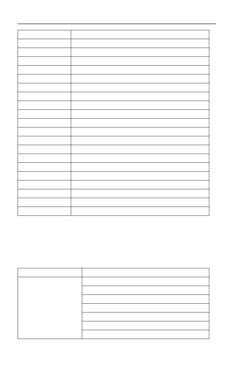
Communication parameter address
The chapter is about communication contents, it’s used to control the inverter operation, the
status of the inverter and related parameter setup. Read and write function code parameters
(Some function codes are not able to be changed, only for the manufacturer use.). The mark
rules of function code parameters address:
The group number and mark of function codes are parameter address for indication rules.
High byte:F0~FF(F group), A0~AF(A group), 70~F(U group)Low byte:00~FF
For example: F3.12, the address indicates F30C
Caution:
Group FF: Parameters could not be read or be modified.
Group U: Parameters could be read but not be modified.
Some parameters can not be changed during operation, some parameters regardless of
the kind of state the inverter in, the parameters can not be changed. Change the function code
parameters, pay attention to the scope of the parameters, units, and relative instructions.
Besides, if EEPROM is frequently stored, it will reduce the service life of EEPROM. In some
communication mode, function code need to be stored as long as changing the RAM value.
Group P: to achieve this function, change high order F of the function code address into 0.
Group A: to achieve this function, change high order A of the function code address to be 4.
Corresponding function code address are indicated below:
High byte: 00~0F(P group), 40~4F(A group)Low byte: 00~FF
For example:
Function code F3.12
can not be stored into EEPROM, address indicates to be
030C,function code A0-05 can not be stored in EEPROM, address indicates to be 4005 ; This
address can only act writing RAM, it can not act reading, when act reading, it is invalid address.
For all parameters, command code 07H can be used to achieve this function.
Stop/running parameter:
Parameter addr.
Parameter description
1000
* Communication setup value(-10000~10000)(Decimal)
1001
Running frequency
1002
Bus voltage
1003
Output voltage
1004
Output current
1005
Output power
1006
Output torque
1007
Running speed
1008
DI input status
1009
DO output status
100A
AI1voltage
100B
AI2 voltage
129
Appendix I H5RS485 Card & RS485Communication Protocol
100C
AI3 voltage
100D
Counting value input
100E
Length value input
100F
Load speed
1010
PID setup
1011
PID feedback
1012
PLC process
1013
PULSE input pulse frequency, unit 0.01kHz
1014
Feedback speed, unit 0.1Hz
1015
Rest running time
1016
AI1 voltage before correction
1017
AI2 voltage before correction
1018
AI3 voltage before correction
1019
Line speed
101A
Current power on time
101B
Current running time
101C
PULSE input pulse frequency, unit 1Hz
101D
Communication setup value
101E
Actual feedback speed
101F
Main frequency X display
1020
Auxiliary frequency Y display
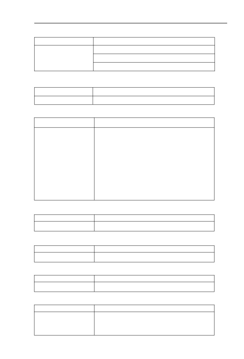
Caution:
The communication setup value is percentage of the relative value,
10000
corresponds
to
100.00% , -10000 corresponds to
-100.00%. For data of dimensional frequency,the
percentage value is the percentage of the maximum frequency. For data of dimensional
torque, the percentage is F2.10, A2.48, A3.48, A4.48
(Torque upper digital setup,
corresponding to the first, second, third, fourth motor).
Control command input to the inverter (write-only)
Command word address
Command function
0001:Forward operation
0002:Reverse operation
0003:Forward jog
2000
0004:Reverse jog
0005:Free stop
0006:Decelerate to stop
0007:Fault reset
130
Appendix I H5RS485 Card & RS485Communication Protocol
Read inverter status:(read-only)
Status word address
Status word function
0001:Forward operation
3000
0002:Reverse operation
0003:Stop
Parameters lock password check:(if the return is the 8888H, it indicates the password
checksum pass)
Password address
Contents of input password
1F00
*****
Digital output terminal control:(write-only)
Command address
Command content
BIT0:DO Output control
BIT1:DO2 Output control
BIT2 RELAY1 Output control
BIT3:RELAY2 Output control
BIT4:FMR Output control
2001
BIT5:VY1
BIT6:VY2
BIT7:VY3
BIT8:VY4
BIT9:VY5
Analog output AO1 control:(write-only)
Command address
Command content
2002
0~7FFF indicates 0%~100%
Analog output AO2control:(write-only)
Command address
Command content
2003
0~7FFF indicates 0%~100%
(PULSE)output control :(write-only)
Command address
Command content
2004
0~7FFFindicates 0%~100%
Inverter fault description:
Inverter fault address
Inverter fault information
0000:No fault
0001:Reserved
8000
0002:Speed-up over current
0003:Speed-down over current
131
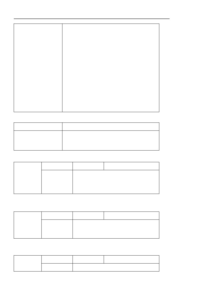
Appendix I H5RS485 Card & RS485Communication Protocol
0004:Constant speed over current
0005:Speed-up over voltage
0006:Speed-DOWN over voltage
0007:Constant speed over voltage
0008:Buffer resistance overload fault
0009:Under-voltage fault
000A:Inverter overload
000B:Motor overload
000C:Input phase lost
000D:Output phase lost
000E:Module overheating
000F:External fault
0010:Communication fault
0011:Contactor fault
0012:Current detection fault
0013:Motor tuning fault
0014:Encoder/PG card fault
0015:Parameter read and write fault
0016:Inverter hardware fault
0017:Motor earthing short-circuit fault
Communication fault information describing data (fault code):
Communication fault address
Fault function description
0000:No fault
0001:Password error
0002:Command code error
0003:CRC check error
8001
0004:Invalid address
0005:Invalid parameter
0006:Parameter change invalid
0007:The system is locked
0008:Operating EEPROM
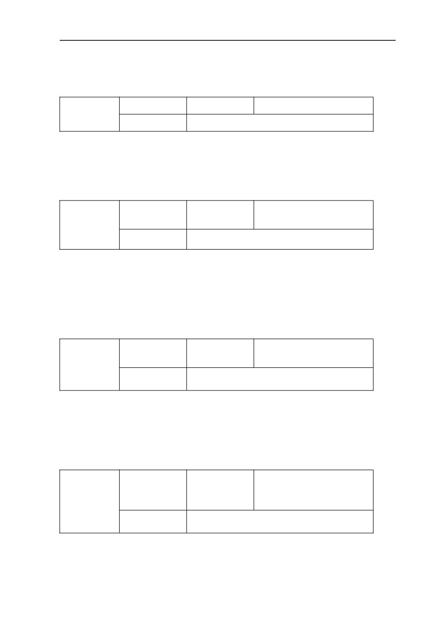
Fd group communication parameters description
Baud rate
Factory default value
6005
1 bit:MODUBS baud rate
0:300BPS
1:600BPS
Fd.00
2:1200BPS
3:2400BPS
Setup range
4:4800BPS
5:9600BPS
6:19200BPS
7:38400BPS
8:57600BPS
9:115200BPS
This parameter is used to set the data transfer rate between the host computer and the
inverter. Caution:The baud rate of the position machine and the inverter must be consistent.
Or,communication is impossible.The higher the baud rate is,the faster the communication is.
Data format
Factory default value
0
0:No check:data format <8,N,2>
Fd.01
1:Even parity check:data format <8,E,1>
Setup range
2:Odd parity check:data format <8,O,1>
3:No check:data format <8-N-1>
The data format of the position machine and the inverter setup must be consistent,
Otherwise communication is impossible.
Local address
Factory default value
1
Fd.02
Setup range
1~247,0 is broadcast address.
132
When the local address is set to 0, that is the broadcast address, achieve position
machine’s broadcast function. The local address is unique (except for the broadcast address),
which is the basis for the position machine and the inverter point to point communication.
Response delay
Factory default value
2ms
Fd.03
Setup range
0~20ms
Response delay: It refers to the interval time from the inverter finishes receiving data to
sending data to the position machine. If the response delay is less than the system processing
time, then the response based on the time delay of the system processing time. If the response
delay is more than the system processing time, after the system process the data, it should be
delayed to wait until the response delay time is up, then sending data to host machine.
Communication
Factory default value
0.0 s
Overtime
Fd.04
0.0 s (Invalid)
Setup range
0.1~60.0s
When the function set to 0.0s, the communication overtime parameter is invalid.
When the function code is set to valid value, if the interval time between one
communication with the next communication exceeded the communications overtime, the
system will report communication fault error
(fault serial
16= E.CoF1)
. Under normal
circumstances, it will be set to invalid value. If the system of continuous communication, setting
parameters, you can monitor the communication status.
Communication
Factory default value
0
protocol selection
Fd.05
0:Non standard Modbus protocol
Setup range
1:Standard Modbus protocol
Fd.05=1:Select Standard Modbus protocol.
Fd.05=0:Reading command, the slave returns the number of bytes which has one more byte
than the standard MODBUS protocol, for specific please refer to the protocol, the part of the "5
communication data structure”.
Communication
read the current
Factory default value
0
Fd.06
resolution
0:0.01A
Setup range
1:0.1A
To determine when the communication reads the output current, what the output current
value unit is.
133
Appendix II Parameter Settings List
Parameters factory default values are shown as below:
Code
Description/Display
Factory setting
Set value 1
Set value 2
U0
Monitor function group: U0.00-U0.61
U0.00
Running frequency
0.01Hz
U0.01
Set frequency
0.01Hz
U0.02
DC bus voltage
0.1V
U0.03
The output voltage
1V
U0.04
Motor output current
0.01A
U0.05
The output power
0.1kW
U0.06
Output torque
0.1%
U0.07
X input status
1
U0.08
Y output status
1
U0.09
AI1 voltage
0.01V
U0.10
AI2 voltage
0.01V
U0.11
AI3 voltage
0.01V
U0.12
Count value
1
U0.13
Length value
1
U0.14
Load speed display
1
U0.15
PID set point
1
U0.16
PID feedback
1
U0.17
PLC stage
1
U0.18
PULSE pulse input frequency
0.01kHz
U0.19
Speed feedback
0.1Hz
U0.20
Surplus running time
0.1Min
U0.21
AI1 voltage before correction
0.001V
U0.22
AI2 voltage before correction
0.001V
U0.23
AI3 voltage before correction
0.001V
U0.24
Linear velocity
1m/Min
U0.25
Current power on time
1Min
U0.26
Current running time
0.1Min
U0.27
PULSE pulse input frequency
1Hz
U0.28
Communication set value
0.01%
U0.29
Encoder feedback speed
0.01Hz
134
Appendix II Parameter Settings List
U0.30
Main frequency X display
0.01Hz
U0.31
Auxiliary frequency Y display
0.01Hz
U0.32
View arbitrary memory address
1
U0.33
Synchronous motor rotor position
0.0°
U0.34
Motor temperature
1℃
U0.35
Target torque
0.1%
U0.36
Rotary variable position
1
U0.37
Power factor angle
0.1
U0.38
ABZ position
0.0
U0.39
VF target voltage separation
1V
U0.40
VF output voltage separation
1V
U0.41
X input status intuitive display
-
U0.42
DO output status intuitive display
-
U0.43
X function status intuitive display1
1
U0.44
X function status intuitive display2
1
U0.45
Fault information
0
U0.46
Reserved
-
U0.47
Reserved
-
U0.48
Reserved
-
U0.58
Z signal counter
-
U0.59
Set frequency
0.01%
U0.60
Running frequency
0.01%
U0.61
Inverter status
1
U0.62
Current fault code
1
U0.63
Point to point communication
0.01%
U0.64
number of Slave
1
U0.65
Torque limit
0.01%
F0
Basic function group:F0.00-F0.28
F0.00
GP type display
-
F0.01
Motor 1 control mode
0
F0.02
Command source selection
0
F0.03
Main frequency source X selection
4
F0.04
Auxiliary frequencysource Y selection
0
F0.05
Auxiliary frequency source Y range selection
0
F0.06
Auxiliary frequency source Y range
100%
135
Appendix II Parameter Settings List
F0.07
Frequency source stacking selection
00
F0.08
Preset frequency
50.00Hz
F0.09
Running direction
0
F0.10
Maximum frequency
50.00Hz
F0.11
Frequency source upper limit
0
F0.12
Frequency upper limit
50.00Hz
F0.13
Frequency upper limit offset
0.00Hz
F0.14
Frequency lower limit
0.00Hz
F0.15
Carrier frequency
-
F0.16
Carrier frequency adjusting with temperature
0
F0.17
Acceleration time 1
-
F0.18
Deceleration time 1
-
F0.19
Acc./ dec. time unit
1
F0.21
Auxiliary frequency source offset frequency
0.00Hz
F0.22
Frequency command resolution
2
F0.23
Digital setup frequency memory selection upon stop
0
F0.24
Motor selection
0
F0.25
Acceleration / deceleration reference frequency
0
F0.26
Frequency UP/DOWNreference upon running
0
F0.27
Command source& frequency source binding
000
F0.28
Communication expansion card
0
F1
Parameters for motor 1: F1.00-F0.37
F1.00
Motor type selection
0
F1.01
Rated power
-
F1.02
Rated voltage
-
F1.03
Rated current
-
F1.04
Rated frequency
-
F1.05
Rated revolving speed
-
F1.06
Asynchronous motor stator resistance
-
F1.07
Asynchronous motor rotor resistance
-
F1.08
Asynchronous motor leakage inductance
-
F1.09
Asynchronous motor mutual inductance
-
F1.10
Asynchronous motor no load current
-
F1.27
Encoder pulses number
2500
F1.28
Encoder type
0
136
Appendix II Parameter Settings List
F1.30
ABZ incremental encoder AB phase
0
F1.31
Encoder installation angle
0.00
F1.32
UVW phase sequence
0
F1.33
UVW encoder offset angle
0.00
F1.34
Rotary transformer pole pairs
1
F1.35
UVW pole-pairs
4
F1.36
PG dropped inspection time
0.0s
F1.37
Tuning selection
0
F2
Vector control function group: F2.00-F2.22
F2.00
Speed loop proportional gain 1
30
F2.01
Speed loop integration time1
0.50s
F2.02
Switching frequency1
5.00Hz
F2.03
Speed loop proportional gain 2
20
F2.04
Speed loop integration time 2
1.00s
F2.05
Switching frequency 2
10.00Hz
F2.06
Vector control slip gain
100%
F2.07
Speed-loop filter time
28
F2.08
Vector control over-excitation gain
64
F2.09
Torque upper limit source in speed control mode
0
F2.10
Torque upper limit digital setup in speed control mode
150.0%
F2.13
Excitation regulation proportional gain
2000
F2.14
Excitation regulation integration gain
1300
F2.15 Torque regulation proportional gain
2000
F2.16 Torque regulation integration gain
1300
F2.17 Speed loop integration attribute
0
F2.18
Synchronous motor field weakening mode
1
F2.19
Synchronous motor field weakening depth
100%
F2.20
Maximum field weakening current
50%
F2.21
Field weakening auto regulation gain
100%
F2.22
Field weakening integration multiples
2
F3
V/F control group: F3.00-F3.15
F3.00
V/F curve setup
0
F3.01
Torque boost value
-
F3.02
Torque boost cut-off frequency
50.00Hz
137
Appendix II Parameter Settings List
F3.03
Multi-point V/F frequency point F1
0.00Hz
F3.04
Multi-point V/F voltage point V1
0.0%
F3.05
Multi-point V/F frequency point F2
0.00Hz
F3.06
Multi-point V/F voltage point V2
0.0%
F3.07
Multi-point V/F frequency point F3
0.00Hz
F3.08
Multi-point V/F voltage point V3
0.0%
F3.09
V/F slip compensation gain
0.0%
F3.10
VF over-excitation gain
64
F3.11
VF oscillation suppression gain
-
F3.13
VF separation voltage source
0
F3.14
VF separation voltage digital setup
0V
F3.15
VF separation voltage rise time
0.0s
F4
Input Terminal: F4.00-F4.39
F4.00
X1terminal function selection
1
F4.01
X2 terminal function selection
4
F4.02
X3 terminal function selection
9
F4.03
X4 terminal function selection
12
F4.04
X5 terminal function selection
0
F4.05
X6 terminal function selection
0
0
F4.06
X7 terminal function selection
F4.07
X8 terminal function selection
0
0
F4.08
X9 terminal function selection
0
F4.09
X10 terminal function selection
F4.10
X filter time
0.010s
F4.11
Terminal command mode
0
F4.12
Terminal UP/DN variation rate
1.00Hz/s
F4.13
AI curve 1 minimum input
0.00V
F4.14
AI curve 1 minimum input corresponding setup
0.0%
F4.15
AI curve 1 maximum input
10.00V
F4.16
AI curve 1 maximum input corresponding setup
100.0%
F4.17
AI1 filter time
0.10s
F4.18
AI curve 2 minimum input
0.00V
F4.19
AI curve 2 minimum input corresponding setup
0.0%
138
Appendix II Parameter Settings List
F4.20
AI curve 2 maximum input
10.00V
F4.21
AI curve 2 maximum input corresponding setup
100.0%
F4.22
AI2 filter time
0.10s
F4.23
AI curve 3 minimum input
0.10V
F4.24
AI curve 3 minimum input corresponding setup
0.0%
F4.25
AI curve3 maximum input
4.00V
F4.26
AI curve 3 maximum input corresponding setup
100.0%
F4.27
AI3filter time
0.10s
F4.28
PULSE minimum input
0.00kHz
F4.29
PULSE minimum input corresponding setup
0.0%
F4.30
PULSE maximum input
50.00
F4.31
PULSE maximum input corresponding setup
100.0%
F4.32
PULSE filter time
0.10s
F4.33
AI curve selection
321
F4.34
AI below minimum input setup selection
000
F4.35
X1 delay time
0.0s
F4.36
X2 delay time
0.0s
F4.37
X3 delay time
0.0s
F4.38
X terminal effective mode selection 1
00000
F4.39
X terminal effective mode selection 2
00000
F5
Output terminal: F5.00-F5.22
F5.00
Y1 terminal output mode selection
0
F5.01
Y1R selection (open collector output terminal )
0
F5.02
Relay output selection(TA1.TB1.TC1)
2
F5.03
Expansion card relay output selection(TA2.TB2.TC2)
0
F5.04
DO1 output selection(open collector output terminal)
1
F5.05
Expansion cardDO2 output selection
4
F5.06
Y1P output selection (pulse output terminal)
0
F5.07
AO1 output selection
0
F5.08
AO2 output selection
1
F5.09
Y1P maximum output frequency
50.00kHz
F5.10
AO1 zero offset
0.0%
F5.11
AO1 gain
1.00
139