Intel 64 and IA-32 Architectures. Software Developer’s Manual (Collection, 2023) - page 151
INTEL® ADVANCED MATRIX EXTENSIONS (INTEL® AMX)
Once one has written two matrices as a sum of lower precision matrices, one can run AMX/TMUL on the
product to approximate the higher precision. But to do this effectively, one needs to have higher precision
accumulation. There are tricks in the literature for doing higher precision all in a lower precision, such as
works on so-called double-double arithmetic. Still, these tend to vary too much from standard matrix-
matrix multiplication to be helpful with TMUL. In the case of Bfloat16, having 32-bit accumulation in the
product allows one to use Bfloat16 to approximate FP32 accuracy.
Therefore, if A = s1*A1 + s2*A2 + s3*A3, and B = t1*B1 + t2*B2 + t3*B3, then A*B can be computed
using AMX/TMUL on the projects Ai*Bj for 1<=i,j<=3, assuming scaling is done carefully to avoid denor-
mals. Assuming FP32 accumulation, the FP32 approximation of A*B can be made by writing out these
lower precision multiplies. Scaling factors can be chosen to avoid denormals at times, but they can also
be picked in a way that simplifies further steps in the algorithm. In some cases, scaling factors can be
chosen to be a power of two, for instance, without significantly reducing the accuracy of the resulting
matrix-matrix multiply.
The number of matrices for A or B are picked depending on the mantissa range to cover. If trying to
emulate FP32 which has 24 bits of mantissa (including the implicit mantissa bit), it is possible with three
Bfloat16 matrices (because each of the triples has 8 bits of mantissa, including the implicit bit.). Here the
range is less important because Bfloat16 and FP32 have the same exponent range. Use three Bfloat16
matrices to approximate FP32 precision by BF16x3. Range issues may still come up for BF16x3 cases
where A has values close to the maximum or minimum exponent for FP32, but that too can be circum-
vented by scaling constants. Scaling factors of 2^24 or 2^(-24) suffice to push it far enough away from
the boundary to make the computation feasible again. This is dependent upon the closest end of the
spectrum.
A few terms from an expansion can also be dropped. For instance, in the BF16x3 case, where there are
three As and three Bs, nine products may result. That is:
A*B = (A1+A2+A3)*(B1+B2+B3) = (A1*B1) + (A1*B2 + A2*B1) + (A1*B3 + A2*B2 + A3*B1) +
(A2*B3 + A3*B2) +(A3*B3).
The parentheses in the last equation are intentionally derived so that all entries in the same “bin” are put
together, and there are nine entries of the form Ai*Bj. This example has five bins, each with its own set
of parentheses. In the Bfloat16 case, |Ai| <= |A_i-1}| / 256. This shows the last two bins (with
A2*B3,A3*B2,A3*B3) are too small to contribute significantly to the answer, which is why if there are Y
terms on each side of A*B, only (Y+1)*Y/2 multiplies are required, not Y*Y multiplies. In this case, drop-
ping the last three (also the difference between Y*Y - (Y+1)*Y/2 when Y=3.) from the nine multiplies.
The last three multiplies in the last two bins have terms less than 2^(-24) as big as the first term. So,
A*B can be approximated (ignoring the scaling terms for now) as the sum of the first three most signifi-
cant bins: A1*B1 + (A1*B2+A2*B1)+(A1*B3+A2*B2*A3*B1). In this case, adding from the least signif-
icant bin to the most significant bin (A1*B1) is recommended.
Whenever A and B are each expanded out to Y-terms, computing only Y*(Y+1)/2 products works under
the condition that each term has the same number of mantissa bits. If some terms have a different
number of bits, then this guideline no longer applies. But for BF16x3, each term covers eight mantissa
bits and Y=3, so six products are needed.
Regarding accuracy, the worst-case relative error for BF16x3 may be worse than FP32. However, BF16x3
tends to cover a larger mantissa range due to implicit bits, which can be more accurate in many cases.
Nevertheless, accuracy is not offered by matrix-matrix multiplication. Even FP64 or FP128 can be bad for
component-wise relative errors. Take A = [1, -1] and B = [1; 1]. A*B is zero. Let eps be a small pertur-
bation to A and/or B. The solution may now be arbitrarily bad in terms of relative error. In general,
assume that the same mantissa range and exponent range is covered as a given higher-precision floating
point format, and the accumulation is at least as good as the higher-precision format. With such an
assumption, the answer will be approximately the same as the higher-precision floating point format. It
may or may not be identical. Performing the same operation in the higher precision format but changing
the order of the computations could yield slightly different results. In terms of matrix-matrix multiplica-
tion, it could yield vast differences in relative error.
Ref#: 248966-048
20-72
INTEL® ADVANCED MATRIX EXTENSIONS (INTEL® AMX)
Things get slightly more complicated if low precision is used to approximate matrix-matrix at FP64 accu-
racy or FP128 precision. Here the scalars aren’t just for avoiding denormals but are necessary to do the
initial matrix conversion. Nevertheless, converting to an integer is recommended in this case because the
FP32-rounded errors in each of the seven or fewer bins may introduce too many errors. An integer is
easier to get right because there are no floating-point errors in each bin.
Conversion to Integer functions in the same way as all of the previous Bfloat16 examples. The quantiza-
tion literature explains how to map floating point numbers into integers. The only difference is that these
integers are further broken down into 8-bit pieces for the use of Intel AMX. Constant factors are still
needed, but in this case they are primarily defined in the conversion itself.
One difficulty with quantization to integers is the notion of a shared exponent. All the numbers quantized
together with shared exponents must share the same range. The assumption is that all of A shares a joint
exponent range. Since this will also be true for B, each row of A and column of B can be quantized sepa-
rately.
Assuming that there is Integer32 accumulation with the Integer8 multiplies, a matrix may be broken
down into far more bits than required. This may significantly reduce the inaccuracy impact of picking a
shared exponent. Because Integer32 arithmetic will be precise, modulo overflow/underflow concerns,
then one can break up A or B into a huge number of 8-bit integer matrices, then do all the matrix-matrix
work with Intel AMX, and then convert back all the results to even get accuracies up to quad-precision.
Considering an extreme case of trying to get over 100-bits of accuracy in a matrix-matrix multiply. All A-
values can be quantified into 128-bit integers. The same holds true with B. Once broken down into 8-bit
quantities, this will have a significant expansion like: A = s1*A1 + s2*A2 + … + s14*A14 for when
attempting 112-bits of mantissa. The same can be done with B = t1*B1 + t2*B2 + … + t14*B14. A*B is
potentially 14*14=196 products, but only 105 products are needed because the last few products may
have scaling factors less than 2^(-112) times the most important terms. Each product term should be
added separately and computing into C from the least significant bits forward.
C15 = (s1*t14)*A1*B14 + (s2*t13)*A2*B13 + … + (s14*t1)*A14*B1
C14 = (s1*t13)*A1*B13 + (s2*t12)*A2*B12 + … + (s13*t1)*A13*B1
C13 = (s1*t12)*A1*B12 + (s2*t11)*A2*B11 + … + (s12*t1)*A12*B1
…
C02 = (s1*t1)*A1*B1
Sometimes choosing scalers is possible such that all the products in a given row can be computed with
the same scratch array. The converted sum of C02 gives the final product through C15, where terms like
C15 should be computed first.
Writing matrix-matrix multiplies in terms of an expansion like (A1+A2+A3)*(B1+B2+B3) is referred to
as “cascading GEMM.” Performance will vary depending on the TMUL/Intel AMX specification, and may
vary from generation to generation. Note that some computations may become bandwidth-bound. Since
there is no quad floating-point precision in hardware for Intel Architecture, the above algorithm may be
competitive performance-wise with other approaches like doing software double-double optimizations or
software-based quad precision.
Ref#: 248966-048
20-73
5.
Updates to Appendix E
Change bars and violet text show changes to Appendix E of the Intel® 64 and IA-32 Architectures Optimization
Reference Manual: The Optimization of Earlier Generations of Intel 64 and IA32 Processor Architectures.
------------------------------------------------------------------------------------------
Changes to this chapter:
• This chapter has been updated to comprise Chapters 1 through 5 of the new Volume 2 of the Intel® 64 and
IA-32 Architectures Optimization Reference Manual.
• Updated capitalization of headings throughout chapter.
• Updated branding throughout chapter.
• Typo and punctuation corrections as necessary.
Intel® 64 and IA-32 Architectures Optimization Reference Manual Documentation Changes
13
CHAPTER 1
HASWELL MICROARCHITECTURE
1.1
INTRODUCTION
The Haswell microarchitecture builds on the successes of the Sandy Bridge and Ivy Bridge microarchitec-
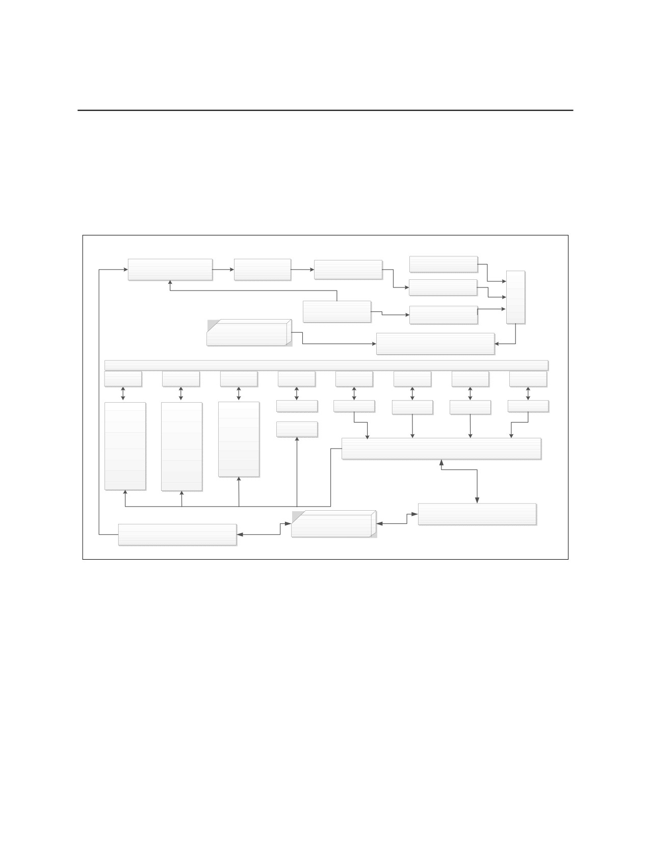
tures. The basic pipeline functionality of the Haswell microarchitecture is depicted in Figure 1-1. In
general, most of the features described in Section 1.2 - Section 1.4 also apply to the Broadwell microar-
chitecture. Enhancements of the Broadwell microarchitecture are summarized in Section 1.6.
MSROM
32K L1 Instruction Cache
Pre-Decode
Instruction Queue
Decoder
IDQ
BPU
Uop Cache (DSB)
Load Buffers, Store
Buffers, Reorder Buffers
Allocate/Rename/Retire/
MoveElimination/ZeroIdiom
Scheduler
Port 0
Port 1
Port 5
Port 6
Port 4
Port 2
Port 3
Port 7
ALU, Shft
STD
LD/STA
LD/STA
STA
ALU,
ALU,
ALU,
SHFT,
Fast LEA,
Fast LEA,
Primary
VEC LOG,
VEC ALU,
VEC ALU,
Branch
VEC SHFT,
VEC LOG,
VEC LOG,
FP mul,
FP mul,
VEC SHUF,
Memory Control
FMA,
FMA,
DIV,
FP add,
STTNI,
Slow Int
Branch2
32K L1 Data Cache
Line Fill Buffers
256K L2 Cache (Unified)
Figure 1-1. CPU Core Pipeline Functionality of the Haswell Microarchitecture
The Haswell microarchitecture offers the following innovative features:
• Support for Intel Advanced Vector Extensions 2 (Intel® AVX2), FMA.
• Support for general-purpose, new instructions to accelerate integer numeric encryption.
• Support for Intel® Transactional Synchronization Extensions (Intel® TSX).
• Each core can dispatch up to 8 micro-ops per cycle.
•
256-bit data path for memory operation, FMA, AVX floating-point and AVX2 integer execution units.
• Improved L1D and L2 cache bandwidth.
• Two FMA execution pipelines.
• Four arithmetic logical units (ALUs).
• Three store address ports.
HASWELL MICROARCHITECTURE
• Two branch execution units.
• Advanced power management features for IA processor core and uncore sub-systems.
• Support for optional fourth level cache.
The microarchitecture supports flexible integration of multiple processor cores with a shared uncore sub-
system consisting of a number of components including a ring interconnect to multiple slices of L3 (an
off-die L4 is optional), processor graphics, integrated memory controller, interconnect fabrics, etc. An
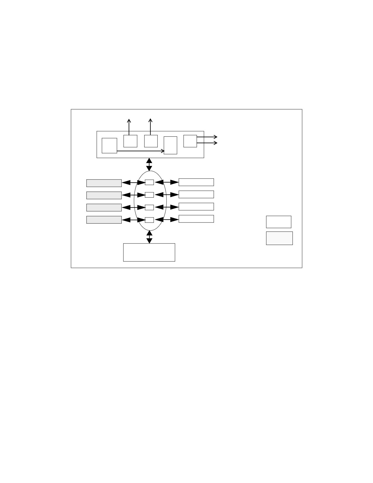
example of the system integration view of four CPU cores with uncore components is illustrated in
Figure 1-2.
PCIe
DMI
DRAM
PEG
DMI
IMc
Disp
PCIe
Eng
Brdg
System Agent
CPU Core
L3 Slice
CPU Core
L3 Slice
CPU Core
L3 Slice
CPU Core
L3 Slice
Legend:
Uncore
CPU Core
Processor Graphics/
Media Engine
Figure 1-2. Four Core System Integration of the Haswell Microarchitecture
1.2
THE FRONT END
The front end of Haswell microarchitecture builds on that of the Sandy Bridge and Ivy Bridge microarchi-
tectures, see Section A.2.2 and Section A.2.7. Additional enhancements in the front end include:
• The uop cache (or decoded ICache) is partitioned equally between two logical processors.
• The instruction decoders will alternate between each active logical processor. If one sibling logical
processor is idle, the active logical processor will use the decoders continuously.
• The LSD in the micro-op queue (or IDQ) can detect small loops up to 56 micro-ops. The 56-entry
micro-op queue is shared by two logical processors if Hyper-Threading Technology is active (Sandy
Bridge microarchitecture provides duplicated 28-entry micro-op queue in each core).
1.3
THE OUT-OF-ORDER ENGINE
The key components and significant improvements to the out-of-order engine are summarized below:
Renamer: The Renamer moves micro-ops from the micro-op queue to bind to the dispatch ports in the
Scheduler with execution resources. Zero-idiom, one-idiom and zero-latency register move operations
are performed by the Renamer to free up the Scheduler and execution core for improved performance.
Ref#: 248966-048
1-2

HASWELL MICROARCHITECTURE
Scheduler: The Scheduler controls the dispatch of micro-ops onto the dispatch ports. There are eight
dispatch ports to support the out-of-order execution core. Four of the eight ports provided execution
resources for computational operations. The other 4 ports support memory operations of up to two 256-
bit load and one 256-bit store operation in a cycle.
Execution Core: The scheduler can dispatch up to eight micro-ops every cycle, one on each port. Of the
four ports providing computational resources, each provides an ALU, two of these execution pipes
provided dedicated FMA units. With the exception of division/square-root, STTNI/AESNI units, most
floating-point and integer SIMD execution units are 256-bit wide. The four dispatch ports servicing
memory operations consist with two dual-use ports for load and store-address operation. Plus a dedi-
cated 3rd store-address port and one dedicated store-data port. All memory ports can handle 256-bit
memory micro-ops. Peak floating-point throughput, at 32 single-precision operations per cycle and 16
double-precision operations per cycle using FMA, is twice that of Sandy Bridge microarchitecture.
The out-of-order engine can handle 192 uops in flight compared to 168 in Sandy Bridge microarchitec-
ture.
1.3.1
Execution Engine
Table 1-1 summarizes which operations can be dispatched on which port.
Table 1-1. Dispatch Port and Execution Stacks of the Haswell Microarchitecture
Port 0
Port 1
Port 2, 3
Port 4
Port 5
Port 6
Port 7
ALU,
ALU,
Load_Addr,
Store_data
ALU,
ALU,
Store_addr,
Simple_AGU
Shift
Fast LEA,
Store_addr
Fast LEA,
Shift,
BM
BM
JEU
SIMD_Log,
SIMD_ALU,
SIMD_ALU,
SIMD misc,
SIMD_Log
SIMD_Log,
SIMD_Shifts
FMA/FP_mul,
FMA/FP_mul,
Shuffle
Divide
FP_add
2nd_Jeu
slow_int,
FP mov,
AES
Table 1-2 lists execution units and common representative instructions that rely on these units. Table 1-2
also includes some instructions that are available only on processors based on the Broadwell microarchi-
tecture.
Ref#: 248966-048
1-3

HASWELL MICROARCHITECTURE
Table 1-2. Haswell Microarchitecture Execution Units and Representative Instructions
Execution
# of
Instructions
Unit
Ports
ALU
4
add, and, cmp, or, test, xor, movzx, movsx, mov, (v)movdqu, (v)movdqa
SHFT
2
sal, shl, rol, adc, sarx, (adcx, adox)1 etc.
Slow Int
1
mul, imul, bsr, rcl, shld, mulx, pdep, etc.
BM
2
andn, bextr, blsi, blsmsk, bzhi, etc
SIMD Log
3
(v)pand, (v)por, (v)pxor, (v)movq, (v)movq, (v)blendp*, vpblendd
SIMD_Shft
1
(v)psl*, (v)psr*
SIMD ALU
2
(v)padd*, (v)psign, (v)pabs, (v)pavgb, (v)pcmpeq*, (v)pmax, (v)pcmpgt*
Shuffle
1
(v)shufp*, vperm*, (v)pack*, (v)unpck*, (v)punpck*, (v)pshuf*, (v)pslldq, (v)alignr, (v)pmovzx*,
vbroadcast*, (v)pslldq, (v)pblendw
SIMD Misc
1
(v)pmul*, (v)pmadd*, STTNI, (v)pclmulqdq, (v)psadw, (v)pcmpgtq, vpsllvd, (v)bendv*, (v)plendw,
FP Add
1
(v)addp*, (v)cmpp*, (v)max*, (v)min*,
FP Mov
1
(v)movap*, (v)movup*, (v)movsd/ss, (v)movd gpr, (v)andp*, (v)orp*
DIVIDE
1
divp*, divs*, vdiv*, sqrt*, vsqrt*, rcp*, vrcp*, rsqrt*, idiv
NOTES:
1. Only available in processors based on the Broadwell microarchitecture and support CPUID ADX feature flag.
The reservation station (RS) is expanded to 60 entries deep (compared to 54 entries in Sandy Bridge
microarchitecture). It can dispatch up to eight micro-ops in one cycle if the micro-ops are ready to
execute. The RS dispatch a micro-op through an issue port to a specific execution cluster, arranged in
several stacks to handle specific data types or granularity of data.
When a source of a micro-op executed in one stack comes from a micro-op executed in another stack, a
delay can occur. The delay occurs also for transitions between Intel SSE integer and Intel SSE floating-
point operations. In some of the cases the data transition is done using a micro-op that is added to the
instruction flow. Table A-25 describes how data, written back after execution, can bypass to micro-op
execution in the following cycles.
Ref#: 248966-048
1-4

HASWELL MICROARCHITECTURE
Table 1-3. Bypass Delay Between Producer and Consumer Micro-ops (cycles)
From/To
INT
SSE-INT/
SSE-FP/
X87/
AVX-INT
AVX-FP_LOW
AVX-FP_High
INT
• micro-op (port 5)
• micro-op (port 5)
micro-op (port 5) + 3
•
micro-op (port 6) +
• micro-op (port 6) + 1
cycle delay
1 cycle
cycle
SSE-INT/
micro-op (port 1)
1 cycle delay
AVX-INT
SSE-FP/
micro-op (port 1)
1 cycle delay
micro-op (port 5) +
AVX-FP_LOW
1cycle delay
X87/
micro-op (port 1) + 3
micro-op (port 5) +
AVX-FP_High
cycle delay
1cycle delay
Load
1 cycle delay
1 cycle delay
2 cycle delay
1.4
CACHE AND MEMORY SUBSYSTEM
The cache hierarchy is similar to prior generations, including an instruction cache, a first-level data cache
and a second-level unified cache in each core, and a 3rd-level unified cache with size dependent on
specific product configuration. The 3rd-level cache is organized as multiple cache slices, the size of each
slice may depend on product configurations, connected by a ring interconnect. The exact details of the
cache topology is reported by CPUID leaf 4. The 3rd level cache resides in the “uncore” sub-system that
is shared by all the processor cores. In some product configurations, a fourth level cache is also
supported. Table A-23 provides more details of the cache hierarchy.
Table 1-4. Cache Parameters of the Haswell Microarchitecture
Capacity /
Line Size
Fastest
Throughput
Peak Bandwidth
Update
Level
Associativity
(bytes)
Latency1
(clocks)
(bytes/cyc)
Policy
First Level Data
32 KB/ 8
64
4 cycle
0.52
64 (Load) + 32
Writeback
(Store)
Instruction
32 KB/8
64
N/A
N/A
N/A
N/A
Second Level
256KB/8
64
11 cycle
Varies
64
Writeback
~34
Third Level (Shared
Varies
64
Varies
Writeback
L3)
NOTES:
1. Software-visible latency will vary depending on access patterns and other factors. L3 latency can vary due to clock ratios
between the processor core and uncore.
2. First level data cache supports two load micro-ops each cycle; each micro-op can fetch up to 32-bytes of data.
Ref#: 248966-048
1-5

HASWELL MICROARCHITECTURE
The TLB hierarchy consists of dedicated level one TLB for instruction cache, TLB for L1D, plus unified TLB
for L2.
Table 1-5. TLB Parameters of the Haswell Microarchitecture
Level
Page Size
Entries
Associativity
Partition
Instruction
4KB
128
4 ways
dynamic
Instruction
2MB/4MB
8 per thread
fixed
First Level Data
4KB
64
4
fixed
First Level Data
2MB/4MB
32
4
fixed
First Level Data
1GB
4
4
fixed
Second Level
Shared by 4KB and 2/4MB pages
1024
8
fixed
1.4.1
Load and Store Operation Enhancements
The L1 data cache can handle two 256-bit load and one 256-bit store operations each cycle. The unified
L2 can service one cache line (64 bytes) each cycle. Additionally, there are 72 load buffers and 42 store
buffers available to support micro-ops execution in-flight.
1.4.2
Unlamination
Some micro-fused instructions cannot be allocated as a single uop, and therefore they break into two
uops in the micro-op queue. The process of breaking a fused instruction into its uops is called unlamina-
tion.
Unlamination will take place if the number of fused instruction sources is greater than three.
Instruction sources in the context of unlamination are considered to be one of the following: memory
address base, memory address index, source register, destination register (including flags), or a source
and destination register.
A memory operand in the context of unlamination can have up to two sources. A memory address in the
x86 instruction set is constructed from: base + index*scale + displacement.
Only a base and an index are counted as instruction sources. Notice that if an index exists, the base is
counted as a source even if it's not present.
In addition, source and destination registers are counted as two sources; this is also true in the case
where the source and destination register are the same.
The following table shows examples of micro-fused instructions and details of unlamination.
Table A-6. Components of the Front End
Instruction Example
Source
Destination
Source and
Index
Base
Number of
Unlaminated
Destination
Sources1
mulss xmm1,
-
-
xmm1
rax
0
3
no
[4*rax+100]
vmulss xmm1, xmm1,
xmm1
xmm1
-
-
rax
3
no
[rax +100]
vmulss xmm1, xmm1,
xmm1
xmm1
-
rax
0
4
yes
[4*rax+100]
cmp rax,
rax
flags
-
rax
rbx
4
yes
[rbx+4*rax+4]
cmp rax, [rbx+4]
rax
flags
-
-
rbx
3
no
NOTES:
1. Recommendation: to avoid unlamination, keep the number of micro-fused instruction sources under 4.
Ref#: 248966-048
1-6
HASWELL MICROARCHITECTURE
1.5
HASWELL-E MICROARCHITECTURE
Intel processors based on the Haswell-E microarchitecture comprises the same processor cores as
described in the Haswell microarchitecture, but provides more advanced uncore and integrated I/O capa-
bilities. Processors based on the Haswell-E microarchitecture support platforms with multiple sockets.
The Haswell-E microarchitecture supports versatile processor architectures and platform configurations
for scalability and high performance. Some of capabilities provided by the uncore and integrated I/O sub-
system of the Haswell-E microarchitecture include:
• Support for multiple Intel QPI interconnects in multi-socket configurations.
• Up to two integrated memory controllers per physical processor.
• Up to 40 lanes of Intel® PCI Express* 3.0 links per physical processor.
• Up to 18 processor cores connected by two ring interconnects to the L3 in each physical processor.
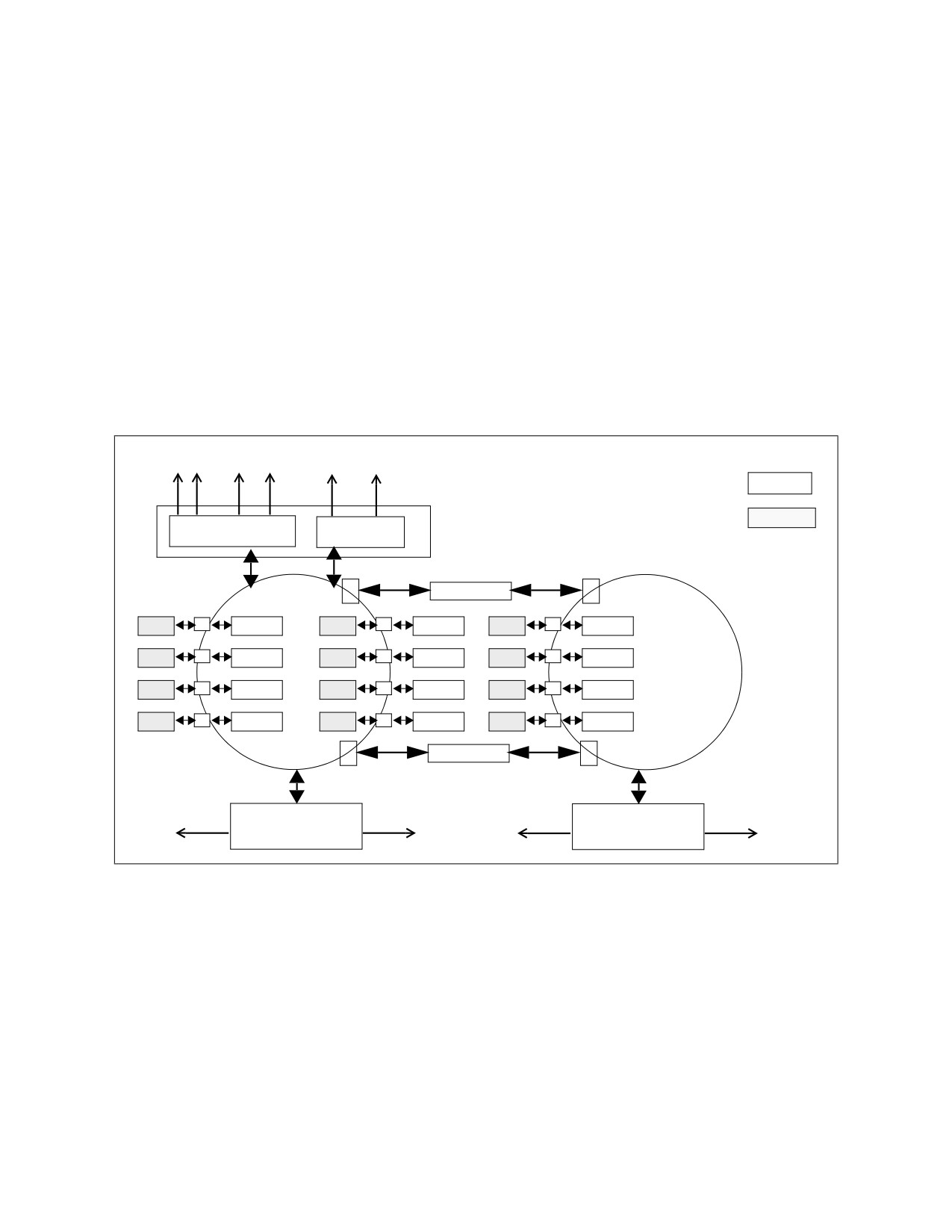
An example of a possible 12-core processor implementation using the Haswell-E microarchitecture is
illustrated in Figure 1-3. The capabilities of the uncore and integrated I/O sub-system vary across the
processor family implementing the Haswell-E microarchitecture. For details, please consult the data
sheets of respective Intel Xeon E5 v3 processors.
Legend:
Uncore
PCIe
QPI
CPU Core
Integrated I/O
QPII Links
Sbox
Core
L3 Slice
Core
L3 Slice
Core
L3 Slice
Core
L3 Slice
Core
L3 Slice
Core
L3 Slice
Core
L3 Slice
Core
L3 Slice
Core
L3 Slice
Core
L3 Slice
Core
L3 Slice
Core
L3 Slice
Sbox
DRAM
Home Agent
DRAM
DRAM
Home Agent
DRAM
Memory Controller
Memory Controller
Figure 1-3. An Example of the Haswell-E Microarchitecture Supporting 12 Processor Cores
1.6
BROADWELL MICROARCHITECTURE
Intel Core M processors are based on the Broadwell microarchitecture. The Broadwell microarchitecture
builds from the Haswell microarchitecture and provides several enhancements. This section covers
enhanced features of the Broadwell microarchitecture.
• Floating-point multiply instruction latency is improved from five cycles in prior generation to three
cycles in the Broadwell microarchitecture. This applies to Intel AVX, Intel SSE and FP instruction sets.
• The throughput of gather instructions has been improved significantly, see Table D-5.
• The PCLMULQDQ instruction implementation is a single uop in the Broadwell microarchitecture with
improved latency and throughput.
Ref#: 248966-048
1-7

HASWELL MICROARCHITECTURE
The TLB hierarchy consists of dedicated level one TLB for instruction cache, TLB for L1D, plus unified TLB
for L2.
Table 1-7. TLB Parameters of the Broadwell Microarchitecture
Level
Page Size
Entries
Associativity
Partition
Instruction
4KB
128
4 ways
dynamic
Instruction
2MB/4MB
8 per thread
fixed
First Level Data
4KB
64
4
fixed
First Level Data
2MB/4MB
32
4
fixed
First Level Data
1GB
4
4
fixed
Second Level
Shared by 4KB and 2MB pages
1536
6
fixed
Second Level
1GB pages
16
4
fixed
Ref#: 248966-048
1-8

CHAPTER 2
SANDY BRIDGE MICROARCHITECTURE
Sandy Bridge microarchitecture builds on the successes of Intel® Core™ microarchitecture and Nehalem
microarchitecture. It offers the following innovative features:
•
Intel Advanced Vector Extensions (Intel AVX)
— 256-bit floating-point instruction set extensions to the 128-bit Intel SSE, providing up to 2X
performance benefits relative to 128-bit code.
— Non-destructive destination encoding offers more flexible coding techniques.
— Supports flexible migration and co-existence between 256-bit AVX code, 128-bit AVX code and
legacy 128-bit SSE code.
•
Enhanced front end and execution engine
— New decoded ICache component that improves front end bandwidth and reduces branch mispre-
diction penalty.
— Advanced branch prediction.
— Additional macro-fusion support.
— Larger dynamic execution window.
— Multi-precision integer arithmetic enhancements (ADC/SBB, MUL/IMUL).
— LEA bandwidth improvement.
— Reduction of general execution stalls (read ports, writeback conflicts, bypass latency, partial
stalls).
— Fast floating-point exception handling.
— XSAVE/XRSTORE performance improvements and XSAVEOPT new instruction.
•
Cache hierarchy improvements for wider data path
— Doubling of bandwidth enabled by two symmetric ports for memory operation.
— Simultaneous handling of more in-flight loads and stores enabled by increased buffers.
— Internal bandwidth of two loads and one store each cycle.
— Improved prefetching.
— High bandwidth low latency LLC architecture.
— High bandwidth ring architecture of on-die interconnect.
•
System-on-a-chip support
— Integrated graphics and media engine in second generation Intel Core processors.
— Integrated Intel® PCIe controller.
— Integrated memory controller.
•
Next generation Intel Turbo Boost Technology
— Leverage TDP headroom to boost performance of CPU cores and integrated graphic unit.
2.1
SANDY BRIDGE MICROARCHITECTURE PIPELINE OVERVIEW
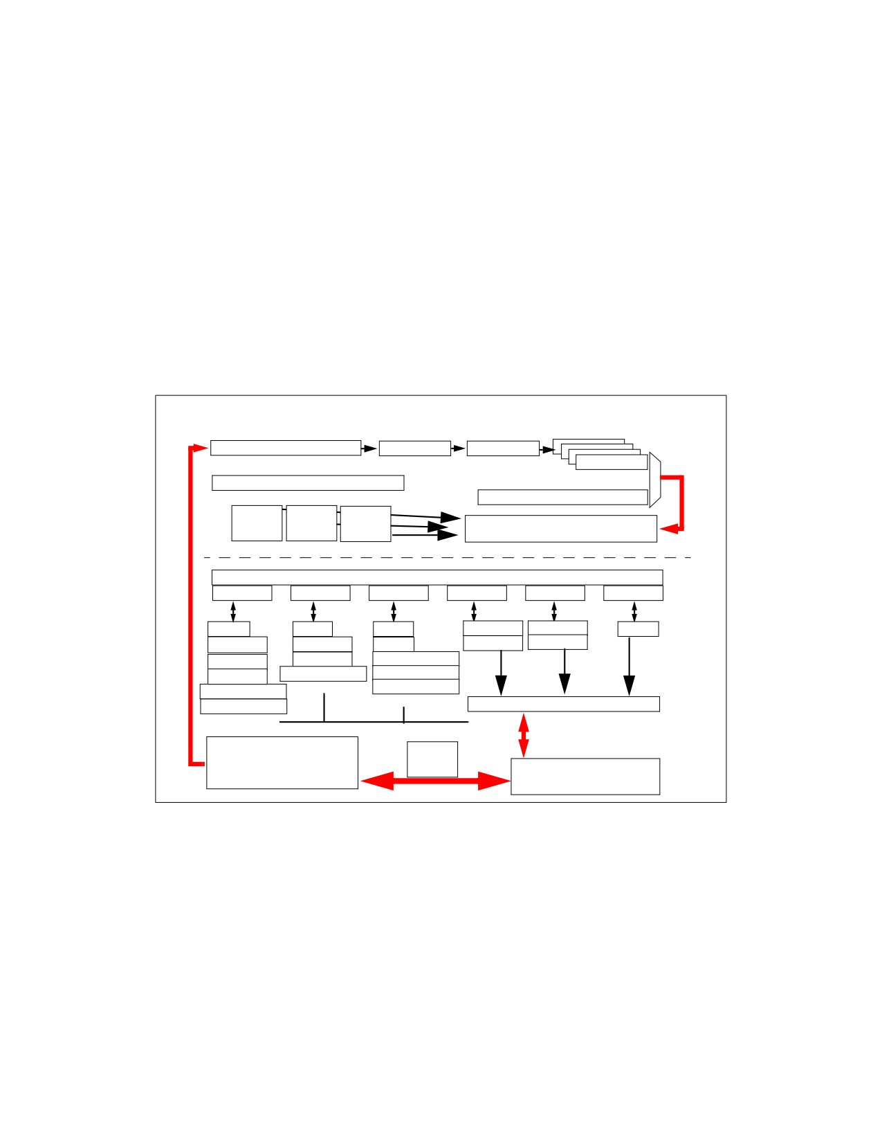
Figure 2-1 depicts the pipeline and major components of a processor core that’s based on Sandy Bridge
microarchitecture. The pipeline consists of:
SANDY BRIDGE MICROARCHITECTURE
• An in-order issue front end that fetches instructions and decodes them into micro-ops (micro-opera-
tions). The front end feeds the next pipeline stages with a continuous stream of micro-ops from the
most likely path that the program will execute.
• An out-of-order, superscalar execution engine that dispatches up to six micro-ops to execution, per
cycle. The allocate/rename block reorders micro-ops to "dataflow" order so they can execute as soon
as their sources are ready and execution resources are available.
• An in-order retirement unit that ensures that the results of execution of the micro-ops, including any
exceptions they may have encountered, are visible according to the original program order.
The flow of an instruction in the pipeline can be summarized in the following progression:
1. The Branch Prediction Unit chooses the next block of code to execute from the program. The
processor searches for the code in the following resources, in this order:
a. Decoded ICache.
b. Instruction Cache, via activating the legacy decode pipeline.
c. L2 cache, last level cache (LLC) and memory, as necessary.
32K L1 Instruction Cache
Pre-decode
Instr Queue
Decoders
Branch Predictor
1.5K uOP Cache
Load
Store
Reorder
Buffers
Buffers
Buffers
Allocate/Rename/Retire
In-order
out-of-order
Scheduler
Port 0
Port 1
Port 5
Port 2
Port 3
Port 4
ALU
ALU
ALU
Load
Load
STD
V-Mul
V-Add
JMP
StAddr
StAddr
V-Shuffle
256- FP Shuf
V-Shuffle
Fdiv
256- FP Add
256- FP Bool
256- FP Blend
256- FP MUL
256- FP Blend
Memory Control
48 bytes/cycle
Line Fill
256K L2 Cache (Unified)
Buffers
32K L1 Data Cache
Figure 2-1. Sandy Bridge Microarchitecture Pipeline Functionality
2.
The micro-ops corresponding to this code are sent to the Rename/retirement block. They enter into
the scheduler in program order, but execute and are de-allocated from the scheduler according to
data-flow order. For simultaneously ready micro-ops, FIFO ordering is nearly always maintained.
Micro-op execution is executed using execution resources arranged in three stacks. The execution
units in each stack are associated with the data type of the instruction.
Branch mispredictions are signaled at branch execution. It re-steers the front end which delivers
micro-ops from the correct path. The processor can overlap work preceding the branch mispre-
diction with work from the following corrected path.
Ref#: 248966-048
2-2

SANDY BRIDGE MICROARCHITECTURE
3. Memory operations are managed and reordered to achieve parallelism and maximum performance.
Misses to the L1 data cache go to the L2 cache. The data cache is non-blocking and can handle
multiple simultaneous misses.
4. Exceptions (Faults, Traps) are signaled at retirement (or attempted retirement) of the faulting
instruction.
Each processor core based on Sandy Bridge microarchitecture can support two logical processor if Intel®
Hyper-Threading Technology (Intel® HT) is enabled.
2.1.1
The Front End
This section describes the key characteristics of the front end. Table B-1 lists the components of the front
end, their functions, and the problems they address.
Table 2-1. Components of the Front End of Sandy Bridge Microarchitecture
Component
Functions
Performance Challenges
Instruction Cache
32-Kbyte backing store of instruction bytes
Fast access to hot code instruction bytes
Provides the same decode latency and
Decode instructions to micro-ops, delivered to
Legacy Decode Pipeline
bandwidth as prior Intel processors.
the micro-op queue and the Decoded ICache.
Decoded ICache warm-up
Provides higher micro-op bandwidth at
Provide stream of micro-ops to the micro-op
Decoded ICache
lower latency and lower power than the
queue.
legacy decode pipeline
Complex instruction micro-op flow store,
MSROM
accessible from both Legacy Decode Pipeline
and Decoded ICache
Determine next block of code to be executed
Improves performance and energy
Branch Prediction Unit
and drive lookup of Decoded ICache and legacy
efficiency through reduced branch
(BPU)
decode pipelines.
mispredictions.
Queues micro-ops from the Decoded ICache
Hide front end bubbles; provide execution
Micro-op queue
and the legacy decode pipeline.
micro-ops at a constant rate.
2.1.1.1
Legacy Decode Pipeline
The Legacy Decode Pipeline comprises the instruction translation lookaside buffer (ITLB), the instruction
cache (ICache), instruction predecode, and instruction decode units.
Instruction Cache and ITLB
An instruction fetch is a 16-byte aligned lookup through the ITLB and into the instruction cache. The
instruction cache can deliver every cycle 16 bytes to the instruction pre-decoder. Table B-1 compares the
ICache and ITLB with prior generation.
Table 2-2. ICache and ITLB of Sandy Bridge Microarchitecture
Component
Sandy Bridge Microarchitecture
Nehalem Microarchitecture
ICache Size
32-Kbyte
32-Kbyte
ICache Ways
8
4
ITLB 4K page entries
128
128
ITLB large page (2M or
8
7
4M) entries
Ref#: 248966-048
2-3
SANDY BRIDGE MICROARCHITECTURE
Upon ITLB miss there is a lookup to the Second level TLB (STLB) that is common to the DTLB and the
ITLB. The penalty of an ITLB miss and a STLB hit is seven cycles.
Instruction PreDecode
The predecode unit accepts the 16 bytes from the instruction cache and determines the length of the
instructions.
The following length changing prefixes (LCPs) imply instruction length that is different from the default
length of instructions. Therefore they cause an additional penalty of three cycles per LCP during length
decoding. Previous processors incur a six-cycle penalty for each 16-byte chunk that has one or more
LCPs in it. Since usually there is no more than one LCP in a 16-byte chunk, in most cases, Sandy Bridge
microarchitecture introduces an improvement over previous processors.
• Operand Size Override (66H) preceding an instruction with a word/double immediate data. This
prefix might appear when the code uses 16 bit data types, unicode processing, and image
processing.
• Address Size Override (67H) preceding an instruction with a modr/m in real, big real, 16-bit
protected or 32-bit protected modes. This prefix may appear in boot code sequences.
• The REX prefix (4xh) in the Intel® 64 instruction set can change the size of two classes of instruc-
tions: MOV offset and MOV immediate. Despite this capability, it does not cause an LCP penalty and
hence is not considered an LCP.
Instruction Decode
There are four decoding units that decode instruction into micro-ops. The first can decode all IA-32 and
Intel 64 instructions up to four micro-ops in size. The remaining three decoding units handle single-
micro-op instructions. All four decoding units support the common cases of single micro-op flows
including micro-fusion and macro-fusion.
Micro-ops emitted by the decoders are directed to the micro-op queue and to the Decoded ICache.
Instructions longer than four micro-ops generate their micro-ops from the MSROM. The MSROM band-
width is four micro-ops per cycle. Instructions whose micro-ops come from the MSROM can start from
either the legacy decode pipeline or from the Decoded ICache.
MicroFusion
Micro-fusion fuses multiple micro-ops from the same instruction into a single complex micro-op. The
complex micro-op is dispatched in the out-of-order execution core as many times as it would if it were
not micro-fused.
Micro-fusion enables you to use memory-to-register operations, also known as the complex instruction
set computer (CISC) instruction set, to express the actual program operation without worrying about a
loss of decode bandwidth. Micro-fusion improves instruction bandwidth delivered from decode to retire-
ment and saves power.
Coding an instruction sequence by using single-uop instructions will increases the code size, which can
decrease fetch bandwidth from the legacy pipeline.
The following are examples of micro-fused micro-ops that can be handled by all decoders.
• All stores to memory, including store immediate. Stores execute internally as two separate functions,
store-address and store-data.
• All instructions that combine load and computation operations (load+op), for example:
• ADDPS XMM9, OWORD PTR [RSP+40]
• FADD DOUBLE PTR [RDI+RSI*8]
• XOR RAX, QWORD PTR [RBP+32]
• All instructions of the form "load and jump," for example:
• JMP [RDI+200]
• RET
• CMP and TEST with immediate operand and memory
An instruction with RIP relative addressing is not micro-fused in the following cases:
Ref#: 248966-048
2-4
SANDY BRIDGE MICROARCHITECTURE
• An additional immediate is needed, for example:
• CMP [RIP+400], 27
• MOV [RIP+3000], 142
• The instruction is a control flow instruction with an indirect target specified using RIP-relative
addressing, for example:
• JMP [RIP+5000000]
In these cases, an instruction that can not be micro-fused will require decoder 0 to issue two micro-ops,
resulting in a slight loss of decode bandwidth.
In 64-bit code, the usage of RIP Relative addressing is common for global data. Since there is no micro-
fusion in these cases, performance may be reduced when porting 32-bit code to 64-bit code.
Macro-Fusion
Macro-fusion merges two instructions into a single micro-op. In Intel Core microarchitecture, this hard-
ware optimization is limited to specific conditions specific to the first and second of the macro-fusable
instruction pair.
• The first instruction of the macro-fused pair modifies the flags. The following instructions can be
macro-fused:
— In Nehalem microarchitecture: CMP, TEST.
— In Sandy Bridge microarchitecture: CMP, TEST, ADD, SUB, AND, INC, DEC
— These instructions can fuse if
• The first source / destination operand is a register.
• The second source operand (if exists) is one of: immediate, register, or non RIP-relative
memory.
• The second instruction of the macro-fusable pair is a conditional branch. Table 3-1 describes, for each
instruction, what branches it can fuse with.
Macro fusion does not happen if the first instruction ends on byte 63 of a cache line, and the second
instruction is a conditional branch that starts at byte 0 of the next cache line.
Since these pairs are common in many types of applications, macro-fusion improves performance even
on non-recompiled binaries.
Each macro-fused instruction executes with a single dispatch. This reduces latency and frees execution
resources. You also gain increased rename and retire bandwidth, increased virtual storage, and power
savings from representing more work in fewer bits.
2.1.2
Decoded ICache
The Decoded ICache is essentially an accelerator of the legacy decode pipeline. By storing decoded
instructions, the Decoded ICache enables the following features:
• Reduced latency on branch mispredictions.
• Increased micro-op delivery bandwidth to the out-of-order engine.
• Reduced front end power consumption.
The Decoded ICache caches the output of the instruction decoder. The next time the micro-ops are
consumed for execution the decoded micro-ops are taken from the Decoded ICache. This enables skip-
ping the fetch and decode stages for these micro-ops and reduces power and latency of the Front End.
The Decoded ICache provides average hit rates of above 80% of the micro-ops; furthermore, "hot spots"
typically have hit rates close to 100%.
Typical integer programs average less than four bytes per instruction, and the front end is able to race
ahead of the back end, filling in a large window for the scheduler to find instruction level parallelism.
However, for high performance code with a basic block consisting of many instructions, for example, Intel
Ref#: 248966-048
2-5
SANDY BRIDGE MICROARCHITECTURE
SSE media algorithms or excessively unrolled loops, the 16 instruction bytes per cycle is occasionally a
limitation. The 32-byte orientation of the Decoded ICache helps such code to avoid this limitation.
The Decoded ICache automatically improves performance of programs with temporal and spatial locality.
However, to fully utilize the Decoded ICache potential, you might need to understand its internal organi-
zation.
The Decoded ICache consists of 32 sets. Each set contains eight Ways. Each Way can hold up to six
micro-ops. The Decoded ICache can ideally hold up to 1536 micro-ops.
The following are some of the rules how the Decoded ICache is filled with micro-ops:
• All micro-ops in a Way represent instructions which are statically contiguous in the code and have
their EIPs within the same aligned 32-byte region.
• Up to three Ways may be dedicated to the same 32-byte aligned chunk, allowing a total of 18 micro-
ops to be cached per 32-byte region of the original IA program.
• A multi micro-op instruction cannot be split across Ways.
• Up to two branches are allowed per Way.
• An instruction which turns on the MSROM consumes an entire Way.
• A non-conditional branch is the last micro-op in a Way.
• Micro-fused micro-ops (load+op and stores) are kept as one micro-op.
• A pair of macro-fused instructions is kept as one micro-op.
• Instructions with 64-bit immediate require two slots to hold the immediate.
When micro-ops cannot be stored in the Decoded ICache due to these restrictions, they are delivered
from the legacy decode pipeline. Once micro-ops are delivered from the legacy pipeline, fetching micro-
ops from the Decoded ICache can resume only after the next branch micro-op. Frequent switches can
incur a penalty.
The Decoded ICache is virtually included in the Instruction cache and ITLB. That is, any instruction with
micro-ops in the Decoded ICache has its original instruction bytes present in the instruction cache.
Instruction cache evictions must also be evicted from the Decoded ICache, which evicts only the neces-
sary lines.
There are cases where the entire Decoded ICache is flushed. One reason for this can be an ITLB entry
eviction. Other reasons are not usually visible to the application programmer, as they occur when
important controls are changed, for example, mapping in CR3, or feature and mode enabling in CR0 and
CR4. There are also cases where the Decoded ICache is disabled, for instance, when the CS base address
is NOT set to zero.
2.1.3
Branch Prediction
Branch prediction predicts the branch target and enables the processor to begin executing instructions
long before the branch true execution path is known. All branches utilize the branch prediction unit (BPU)
for prediction. This unit predicts the target address not only based on the EIP of the branch but also
based on the execution path through which execution reached this EIP. The BPU can efficiently predict the
following branch types:
• Conditional branches.
• Direct calls and jumps.
• Indirect calls and jumps.
• Returns.
2.1.4
Micro-op Queue and the Loop Stream Detector (LSD)
The micro-op queue decouples the front end and the out-of order engine. It stays between the micro-op
generation and the renamer as shown in Figure 2-1. This queue helps to hide bubbles which are intro-
Ref#: 248966-048
2-6
SANDY BRIDGE MICROARCHITECTURE
duced between the various sources of micro-ops in the front end and ensures that four micro-ops are
delivered for execution, each cycle.
The micro-op queue provides post-decode functionality for certain instructions types. In particular, loads
combined with computational operations and all stores, when used with indexed addressing, are repre-
sented as a single micro-op in the decoder or Decoded ICache. In the micro-op queue they are frag-
mented into two micro-ops through a process called un-lamination, one does the load and the other does
the operation. A typical example is the following "load plus operation" instruction:
ADD
RAX, [RBP+RSI]; rax := rax + LD( RBP+RSI )
Similarly, the following store instruction has three register sources and is broken into "generate store
address" and "generate store data" sub-components.
MOV
[ESP+ECX*4+12345678], AL
The additional micro-ops generated by unlamination use the rename and retirement bandwidth.
However, it has an overall power benefit. For code that is dominated by indexed addressing (as often
happens with array processing), recoding algorithms to use base (or base+displacement) addressing can
sometimes improve performance by keeping the load plus operation and store instructions fused.
The Loop Stream Detector (LSD)
The Loop Stream Detector was introduced in Intel® Core microarchitectures. The LSD detects small loops
that fit in the micro-op queue and locks them down. The loop streams from the micro-op queue, with no
more fetching, decoding, or reading micro-ops from any of the caches, until a branch mis-prediction
inevitably ends it.
The loops with the following attributes qualify for LSD/micro-op queue replay:
• Up to eight chunk fetches of 32-instruction-bytes.
• Up to 28 micro-ops (~28 instructions).
• All micro-ops are also resident in the Decoded ICache.
• Can contain no more than eight taken branches and none of them can be a CALL or RET.
• Cannot have mismatched stack operations. For example, more PUSH than POP instructions.
Many calculation-intensive loops, searches and software string moves match these characteristics.
Use the loop cache functionality opportunistically. For high performance code, loop unrolling is generally
preferable for performance even when it overflows the LSD capability.
2.2
THE OUT-OF-ORDER ENGINE
The Out-of-Order engine provides improved performance over prior generations with excellent power
characteristics. It detects dependency chains and sends them to execution out-of-order while main-
taining the correct data flow. When a dependency chain is waiting for a resource, such as a second-level
data cache line, it sends micro-ops from another chain to the execution core. This increases the overall
rate of instructions executed per cycle (IPC).
The out-of-order engine consists of two blocks, shown in Figure 2-1: Core Functional Diagram, the
Rename/retirement block, and the Scheduler.
The Out-of-Order (OOO) engine contains the following major components:
Renamer. The Renamer component moves micro-ops from the front end to the execution core. It elimi-
nates false dependencies among micro-ops, thereby enabling out-of-order execution of micro-ops.
Scheduler. The Scheduler component queues micro-ops until all source operands are ready. Schedules
and dispatches ready micro-ops to the available execution units in as close to a first in first out (FIFO)
order as possible.
Retirement. The Retirement component retires instructions and micro-ops in order and handles faults
and exceptions.
Ref#: 248966-048
2-7
SANDY BRIDGE MICROARCHITECTURE
2.2.1
Renamer
The Renamer is the bridge between the in-order part in Figure 2-1, and the dataflow world of the Sched-
uler. It moves up to four micro-ops every cycle from the micro-op queue to the out-of-order engine.
Although the renamer can send up to 4 micro-ops (unfused, micro-fused, or macro-fused) per cycle, this
is equivalent to the issue port can dispatch six micro-ops per cycle. In this process, the out-of-order core
carries out the following steps:
• Renames architectural sources and destinations of the micro-ops to micro-architectural sources and
destinations.
• Allocates resources to the micro-ops. For example, load or store buffers.
• Binds the micro-op to an appropriate dispatch port.
Some micro-ops can execute to completion during rename and are removed from the pipeline at that
point, effectively costing no execution bandwidth. These include:
• Zero idioms (dependency breaking idioms).
• NOP.
• VZEROUPPER.
• FXCHG.
The renamer can allocate two branches each cycle, compared to one branch each cycle in the previous
microarchitecture. This can eliminate some bubbles in execution.
Micro-fused load and store operations that use an index register are decomposed to two micro-ops,
hence consume two out of the four slots the Renamer can use every cycle.
Dependency Breaking Idioms
Instruction parallelism can be improved by using common instructions to clear register contents to zero.
The renamer can detect them on the zero evaluation of the destination register.
Use one of these dependency breaking idioms to clear a register when possible.
• XOR REG,REG
• SUB REG,REG
• PXOR/VPXOR XMMREG,XMMREG
• PSUBB/W/D/Q XMMREG,XMMREG
• VPSUBB/W/D/Q XMMREG,XMMREG
• XORPS/PD XMMREG,XMMREG
• VXORPS/PD YMMREG, YMMREG
Since zero idioms are detected and removed by the renamer, they have no execution latency.
There is another dependency breaking idiom - the "ones idiom".
• CMPEQ
XMM1, XMM1; "ones idiom" set all elements to all "ones"
In this case, the micro-op must execute, however, since it is known that regardless of the input data the
output data is always "all ones" the micro-op dependency upon its sources does not exist as with the zero
idiom and it can execute as soon as it finds a free execution port.
2.2.2
Scheduler
The scheduler controls the dispatch of micro-ops onto their execution ports. In order to do this, it must
identify which micro-ops are ready and where its sources come from: a register file entry, or a bypass
directly from an execution unit. Depending on the availability of dispatch ports and writeback buses, and
the priority of ready micro-ops, the scheduler selects which micro-ops are dispatched every cycle.
Ref#: 248966-048
2-8

SANDY BRIDGE MICROARCHITECTURE
2.2.3
The Execution Core
The execution core is superscalar and can process instructions out of order. The execution core optimizes
overall performance by handling the most common operations efficiently, while minimizing potential
delays.
The out-of-order execution core improves execution unit organization over prior generation in the
following ways:
• Reduction in read port stalls.
• Reduction in writeback conflicts and delays.
• Reduction in power.
• Reduction of SIMD FP assists dealing with denormal inputs and underflow outputs.
Some high precision FP algorithms need to operate with FTZ=0 and DAZ=0, i.e. permitting underflow
intermediate results and denormal inputs to achieve higher numerical precision at the expense of
reduced performance on prior generation microarchitectures due to SIMD FP assists. The reduction of
SIMD FP assists in Sandy Bridge microarchitecture applies to the following Intel SSE instructions (and
Intel AVX variants): ADDPD/ADDPS, MULPD/MULPS, DIVPD/DIVPS, and CVTPD2PS.
The out-of-order core consist of three execution stacks, where each stack encapsulates a certain type of
data. The execution core contains the following execution stacks:
• General purpose integer.
• SIMD integer and floating-point.
• X87.
The execution core also contains connections to and from the cache hierarchy. The loaded data is fetched
from the caches and written back into one of the stacks.
The scheduler can dispatch up to six micro-ops every cycle, one on each port. The following table
summarizes which operations can be dispatched on which port.
Table 2-3. Dispatch Port and Execution Stacks
Port 0
Port 1
Port 2
Port 3
Port 4
Port 5
ALU,
ALU,
Fast LEA,
Load_Addr,
Load_Addr
Shift,
Integer
ALU, Shift
Store_data
Slow LEA,
Store_addr
Store_addr
Branch,
MUL
Fast LEA
SSE-Int,
Mul, Shift,
ALU, Shuf,
ALU, Shuf,
AVX-Int,
STTNI, Int-Div,
Blend, 128b-
Store_data
Shift, Blend,
128b-Mov
Mov
128b-Mov
MMX
SSE-FP,
Mul, Div, Blend,
Shuf, Blend,
Add, CVT
Store_data
AVX-FP_low
256b-Mov
256b-Mov
X87,
Mul, Div, Blend,
Shuf, Blend,
Add, CVT
Store_data
AVX-FP_High
256b-Mov
256b-Mov
After execution, the data is written back on a writeback bus corresponding to the dispatch port and the
data type of the result. Micro-ops that are dispatched on the same port but have different latencies may
need the write back bus at the same cycle. In these cases the execution of one of the micro-ops is
delayed until the writeback bus is available. For example, MULPS (five cycles) and BLENDPS (one cycle)
may collide if both are ready for execution on port 0: first the MULPS and four cycles later the BLENDPS.
Sandy Bridge microarchitecture eliminates such collisions as long as the micro-ops write the results to
Ref#: 248966-048
2-9

SANDY BRIDGE MICROARCHITECTURE
different stacks. For example, integer ADD (one cycle) can be dispatched four cycles after MULPS (five
cycles) since the integer ADD uses the integer stack while the MULPS uses the FP stack.
When a source of a micro-op executed in one stack comes from a micro-op executed in another stack, a
one- or two-cycle delay can occur. The delay occurs also for transitions between Intel SSE integer and
Intel SSE floating-point operations. In some of the cases the data transition is done using a micro-op that
is added to the instruction flow. The following table describes how data, written back after execution, can
bypass to micro-op execution in the following cycles.
Table 2-4. Execution Core Writeback Latency (cycles)
SSE-Int, AVX-Int,
SSE-FP,
X87,
Integer
MMX
AVX-FP_low
AVX-FP_High
micro-op (port 0) +
Integer
0
micro-op (port 0)
micro-op (port 0)
1 cycle
micro-op (port 5) or
SSE-Int, AVX-Int,
micro-op (port 5) +1
0
1 cycle delay
0
MMX
cycle
micro-op (port 5) or
SSE-FP,
1 cycle delay
micro-op (port 5) +1
micro-op (port 5) +1
0
AVX-FP_low
cycle
cycle
X87,
micro-op (port 5) +1
micro-op (port 5)
0
0
AVX-FP_High
cycle
+1 cycle
Load
0
1 cycle delay
1 cycle delay
2 cycle delay
2.3
CACHE HIERARCHY
The cache hierarchy contains a first level instruction cache, a first level data cache (L1 DCache) and a
second level (L2) cache, in each core. The L1D cache may be shared by two logical processors if the
processor support Intel HT. The L2 cache is shared by instructions and data. All cores in a physical
processor package connect to a shared last level cache (LLC) via a ring connection.
The caches use the services of the Instruction Translation Lookaside Buffer (ITLB), Data Translation
Lookaside Buffer (DTLB) and Shared Translation Lookaside Buffer (STLB) to translate linear addresses to
physical address. Data coherency in all cache levels is maintained using the MESI protocol. For more
information, see the Intel® 64 IA-32 Architectures Software Developer's Manual, Volume 3. Cache hier-
archy details can be obtained at run-time using the CPUID instruction. see the Intel® 64 and IA-32
Architectures Software Developer’s Manual, Volume 2A.
Table 2-5. Cache Parameters
Associativity
Line Size
Write Update
Level
Capacity
Inclusive
(ways)
(bytes)
Policy
L1 Data
32 KB
8
64
Writeback
-
Instruction
32 KB
8
N/A
N/A
-
L2 (Unified)
256 KB
8
64
Writeback
No
Varies, query
Varies with cache
Third Level (LLC)
64
Writeback
Yes
CPUID leaf 4
size
Ref#: 248966-048
2-10

SANDY BRIDGE MICROARCHITECTURE
2.3.1
Load and Store Operation Overview
This section provides an overview of the load and store operations.
Loads
When an instruction reads data from a memory location that has write-back (WB) type, the processor
looks for it in the caches and memory. Table 2-6 shows the access lookup order and best case latency.
The actual latency can vary depending on the cache queue occupancy, LLC ring occupancy, memory
components, and their parameters.
Table 2-6. Lookup Order and Load Latency
Level
Latency (cycles)
Bandwidth (per core per cycle)
L1 Data
41
2 x16 bytes
L2 (Unified)
12
1 x 32 bytes
Third Level (LLC)
26-312
1 x 32 bytes
L2 and L1 DCache in other cores
43- clean hit;
if applicable
60 - dirty hit
NOTES:
1. Subject to execution core bypass restriction shown in Table 2-4.
2. Latency of L3 varies with product segment and sku. The values apply to second generation Intel Core processor families.
The LLC is inclusive of all cache levels above it - data contained in the core caches must also reside in the
LLC. Each cache line in the LLC holds an indication of the cores that may have this line in their L2 and L1
caches. If there is an indication in the LLC that other cores may hold the line of interest and its state
might have to modify, there is a lookup into the L1 DCache and L2 of these cores too. The lookup is called
“clean” if it does not require fetching data from the other core caches. The lookup is called “dirty” if modi-
fied data has to be fetched from the other core caches and transferred to the loading core.
The latencies shown above are the best-case scenarios. Sometimes a modified cache line has to be
evicted to make space for a new cache line. The modified cache line is evicted in parallel to bringing the
new data and does not require additional latency. However, when data is written back to memory, the
eviction uses cache bandwidth and possibly memory bandwidth as well. Therefore, when multiple cache
misses require the eviction of modified lines within a short time, there is an overall degradation in cache
response time. Memory access latencies vary based on occupancy of the memory controller queues,
DRAM configuration, DDR parameters, and DDR paging behavior (if the requested page is a page-hit,
page-miss or page-empty).
Stores
When an instruction writes data to a memory location that has a write back memory type, the processor
first ensures that it has the line containing this memory location in its L1 DCache, in Exclusive or Modified
MESI state. If the cache line is not there, in the right state, the processor fetches it from the next levels
of the memory hierarchy using a Read for Ownership request. The processor looks for the cache line in
the following locations, in the specified order:
1. L1 DCache
2. L2
3. Last Level Cache
4. L2 and L1 DCache in other cores, if applicable
5. Memory
Once the cache line is in the L1 DCache, the new data is written to it, and the line is marked as Modified.
Reading for ownership and storing the data happens after instruction retirement and follows the order of
store instruction retirement. Therefore, the store latency usually does not affect the store instruction
itself. However, several sequential stores that miss the L1 DCache may have cumulative latency that can
Ref#: 248966-048
2-11

SANDY BRIDGE MICROARCHITECTURE
affect performance. As long as the store does not complete, its entry remains occupied in the store
buffer. When the store buffer becomes full, new micro-ops cannot enter the execution pipe and execution
might stall.
2.3.2
L1 DCache
The L1 DCache is the first level data cache. It manages all load and store requests from all types through
its internal data structures. The L1 DCache:
• Enables loads and stores to issue speculatively and out of order.
• Ensures that retired loads and stores have the correct data upon retirement.
• Ensures that loads and stores follow the memory ordering rules of the IA-32 and Intel 64 instruction
set architecture.
Table 2-7. L1 Data Cache Components
Component
Sandy Bridge Microarchitecture
Nehalem Microarchitecture
Data Cache Unit (DCU)
32KB, 8 ways
32KB, 8 ways
Load buffers
64 entries
48 entries
Store buffers
36 entries
32 entries
Line fill buffers (LFB)
10 entries
10 entries
The DCU is organized as 32 KBytes, eight-way set associative. Cache line size is 64-bytes arranged in
eight banks.
Internally, accesses are up to 16 bytes, with 256-bit Intel AVX instructions utilizing two 16-byte
accesses. Two load operations and one store operation can be handled each cycle.
The L1 DCache maintains requests which cannot be serviced immediately to completion. Some reasons
for requests that are delayed: cache misses, unaligned access that splits across cache lines, data not
ready to be forwarded from a preceding store, loads experiencing bank collisions, and load block due to
cache line replacement.
The L1 DCache can maintain up to 64 load micro-ops from allocation until retirement. It can maintain up
to 36 store operations from allocation until the store value is committed to the cache, or written to the
line fill buffers (LFB) in the case of non-temporal stores.
The L1 DCache can handle multiple outstanding cache misses and continue to service incoming stores
and loads. Up to 10 requests of missing cache lines can be managed simultaneously using the LFB.
The L1 DCache is a write-back write-allocate cache. Stores that hit in the DCU do not update the lower
levels of the memory hierarchy. Stores that miss the DCU allocate a cache line.
Ref#: 248966-048
2-12

SANDY BRIDGE MICROARCHITECTURE
Loads
The L1 DCache architecture can service two loads per cycle, each of which can be up to 16 bytes. Up to
32 loads can be maintained at different stages of progress, from their allocation in the out of order engine
until the loaded value is returned to the execution core.
Loads can:
• Read data before preceding stores when the load address and store address ranges are known not to
conflict.
• Be carried out speculatively, before preceding branches are resolved.
• Take cache misses out of order and in an overlapped manner.
Loads cannot:
• Speculatively take any sort of fault or trap.
• Speculatively access uncacheable memory.
The common load latency is five cycles. When using a simple addressing mode, base plus offset that is
smaller than 2048, the load latency can be four cycles. This technique is especially useful for pointer-
chasing code. However, overall latency varies depending on the target register data type due to stack
bypass. See Section 2.2.3 for more information.
The following table lists overall load latencies. These latencies assume the common case of flat segment,
that is, segment base address is zero. If segment base is not zero, load latency increases.
Table 2-8. Effect of Addressing Modes on Load Latency
Base + Offset > 2048;
Data Type/Addressing Mode
Base + Index [+ Offset]
Base + Offset < 2048
Integer
5
4
MMX, SSE, 128-bit AVX
6
5
X87
7
6
256-bit AVX
7
7
Stores
Stores to memory are executed in two phases:
• Execution phase. Fills the store buffers with linear and physical address and data. Once store address
and data are known, the store data can be forwarded to the following load operations that need it.
• Completion phase. After the store retires, the L1 DCache moves its data from the store buffers to the
DCU, up to 16 bytes per cycle.
Address Translation
The DTLB can perform three linear to physical address translations every cycle, two for load addresses
and one for a store address. If the address is missing in the DTLB, the processor looks for it in the STLB,
which holds data and instruction address translations. The penalty of a DTLB miss that hits the STLB is
seven cycles. Large page support include 1G byte pages, in addition to 4K and 2M/4M pages.
The DTLB and STLB are four way set associative. The following table specifies the number of entries in
the DTLB and STLB.
Ref#: 248966-048
2-13

SANDY BRIDGE MICROARCHITECTURE
Table 2-9. DTLB and STLB Parameters
TLB
Page Size
Entries
DTLB
4KB
64
2MB/4MB
32
1GB
4
STLB
4KB
512
Store Forwarding
If a load follows a store and reloads the data that the store writes to memory, the data can forward
directly from the store operation to the load. This process, called store to load forwarding, saves cycles
by enabling the load to obtain the data directly from the store operation instead of through memory. You
can take advantage of store forwarding to quickly move complex structures without losing the ability to
forward the subfields. The memory control unit can handle store forwarding situations with less restric-
tions compared to previous micro-architectures.
The following rules must be met to enable store to load forwarding:
• The store must be the last store to that address, prior to the load.
• The store must contain all data being loaded.
• The load is from a write-back memory type and neither the load nor the store are non-temporal
accesses.
Stores cannot forward to loads in the following cases:
• Four byte and eight byte loads that cross eight byte boundary, relative to the preceding 16- or 32-
byte store.
• Any load that crosses a 16-byte boundary of a 32-byte store.
Table 2-10 to Table 2-13 detail the store to load forwarding behavior. For a given store size, all the loads
that may overlap are shown and specified by ‘F’. Forwarding from 32 byte store is similar to forwarding
from each of the 16 byte halves of the store. Cases that cannot forward are shown as ‘N’.
Table 2-10. Store Forwarding Conditions (1 and 2 byte stores)
Load Alignment
Store
Load
0
1
2
3
4
5
6
7
8
9
10
11
12
13
14
15
Size
Size
1
1
F
2
1
F
F
2
F
N
Ref#: 248966-048
2-14

SANDY BRIDGE MICROARCHITECTURE
Table 2-11. Store Forwarding Conditions (4-16 byte stores)
Load Alignment
Store
Load
0
1
2
3
4
5
6
7
8
9
10
11
12
13
14
15
Size
Size
4
1
F
F
F
F
2
F
F
F
N
4
F
N
N
N
8
1
F
F
F
F
F
F
F
F
2
F
F
F
F
F
F
F
N
4
F
F
F
F
F
N
N
N
8
F
N
N
N
N
N
N
N
16
1
F
F
F
F
F
F
F
F
F
F
F
F
F
F
F
F
2
F
F
F
F
F
F
F
F
F
F
F
F
F
F
F
N
4
F
F
F
F
F
N
N
N
F
F
F
F
F
N
N
N
8
F
N
N
N
N
N
N
N
F
N
N
N
N
N
N
N
16
F
N
N
N
N
N
N
N
N
N
N
N
N
N
N
N
Table 2-12. 32-byte Store Forwarding Conditions (0-15 byte alignment)
Load Alignment
Store
Load
0
1
2
3
4
5
6
7
8
9
10
11
12
13
14
15
Size
Size
32
1
F
F
F
F
F
F
F
F
F
F
F
F
F
F
F
F
2
F
F
F
F
F
F
F
F
F
F
F
F
F
F
F
N
4
F
F
F
F
F
N
N
N
F
F
F
F
F
N
N
N
8
F
N
N
N
N
N
N
N
F
N
N
N
N
N
N
N
16
F
N
N
N
N
N
N
N
N
N
N
N
N
N
N
N
32
F
N
N
N
N
N
N
N
N
N
N
N
N
N
N
N
Table 2-13. 32-byte Store Forwarding Conditions (16-31 byte alignment)
Load Alignment
Store
Load
16
17
18
19
20
21
22
23
24
25
26
27
28
29
30
31
Size
Size
32
1
F
F
F
F
F
F
F
F
F
F
F
F
F
F
F
F
2
F
F
F
F
F
F
F
F
F
F
F
F
F
F
F
N
4
F
F
F
F
F
N
N
N
F
F
F
F
F
N
N
N
8
F
N
N
N
N
N
N
N
F
N
N
N
N
N
N
N
16
F
N
N
N
N
N
N
N
N
N
N
N
N
N
N
N
32
N
N
N
N
N
N
N
N
N
N
N
N
N
N
N
N
Ref#: 248966-048
2-15
SANDY BRIDGE MICROARCHITECTURE
Memory Disambiguation
A load operation may depend on a preceding store. Many microarchitectures block loads until all
preceding store addresses are known. The memory disambiguator predicts which loads will not depend
on any previous stores whose addresses aren’t yet known. When the disambiguator predicts that a load
does not have such a dependency, the load takes its data from an earlier store to the same address. This
hides the load latency. Eventually, the prediction is verified. If the load did indeed depend on a store
whose address was unknown at the time the load executed, this conflict is detected and the load and all
succeeding instructions are re-executed.
The following loads are not disambiguated. The execution of these loads is stalled until addresses of all
previous stores are known.
• Loads that cross the 16-byte aligned boundary, other than 32-byte loads.
•
32-byte Intel AVX loads that are not 32-byte aligned.
Bank Conflict
Since 16-byte loads can cover up to three banks, and two loads can happen every cycle, it is possible that
six of the eight banks may be accessed per cycle, for loads. A bank conflict happens when two load
accesses need the same bank (their address has the same 2-4 bit value) in different sets, at the same
time. When a bank conflict occurs, one of the load accesses is recycled internally.
In many cases two loads access exactly the same bank in the same cache line, as may happen when
popping operands off the stack, or any sequential accesses. In these cases, conflict does not occur and
the loads are serviced simultaneously.
2.3.2.1
Ring Interconnect and Last Level Cache
The system-on-a-chip design provides a high bandwidth bi-directional ring bus to connect between the
IA cores and various sub-systems in the uncore. In the second generation Intel Core processor 2xxx
series, the uncore subsystem include a system agent, the graphics unit (GT) and the last level cache
(LLC).
The LLC consists of multiple cache slices. The number of slices is equal to the number of IA cores. Each
slice has logic portion and data array portion. The logic portion handles data coherency, memory
ordering, access to the data array portion, LLC misses and writeback to memory, and more. The data
array portion stores cache lines. Each slice contains a full cache port that can supply 32 bytes/cycle.
The physical addresses of data kept in the LLC data arrays are distributed among the cache slices by a
hash function, such that addresses are uniformly distributed. The data array in a cache block may have
4/8/12/16 ways corresponding to 0.5M/1M/1.5M/2M block size. However, due to the address distribution
among the cache blocks from the software point of view, this does not appear as a normal N-way cache.
From the processor cores and the GT view, the LLC act as one shared cache with multiple ports and band-
width that scales with the number of cores. The LLC hit latency, ranging between 26-31 cycles, depends
on the core location relative to the LLC block, and how far the request needs to travel on the ring.
The number of cache-slices increases with the number of cores, therefore the ring and LLC are not likely
to be a bandwidth limiter to core operation.
The GT sits on the same ring interconnect, and uses the LLC for its data operations as well. In this respect
it is very similar to an IA core. Therefore, high bandwidth graphic applications using cache bandwidth and
significant cache footprint, can interfere, to some extent, with core operations.
All the traffic that cannot be satisfied by the LLC, such as LLC misses, dirty line writeback, non-cacheable
operations, and MMIO/IO operations, still travels through the cache-slice logic portion and the ring, to
the system agent.
In the Intel Xeon Processor E5 Family, the uncore subsystem does not include the graphics unit (GT).
Instead, the uncore subsystem contains many more components, including an LLC with larger capacity
and snooping capabilities to support multiple processors, Intel® QuickPath Interconnect interfaces that
can support multi-socket platforms, power management control hardware, and a system agent capable
of supporting high-bandwidth traffic from memory and I/O devices.
Ref#: 248966-048
2-16
SANDY BRIDGE MICROARCHITECTURE
In the Intel Xeon processor E5 2xxx or 4xxx families, the LLC capacity generally scales with the number
of processor cores with 2.5 MBytes per core.
2.3.2.2
Data Prefetching
Data can be speculatively loaded to the L1 DCache using software prefetching, hardware prefetching, or
any combination of the two.
You can use the four Streaming SIMD Extensions (SSE) prefetch instructions to enable software-
controlled prefetching. These instructions are hints to bring a cache line of data into the desired levels of
the cache hierarchy. The software-controlled prefetch is intended for prefetching data, but not for
prefetching code.
The rest of this section describes the various hardware prefetching mechanisms provided by Sandy
Bridge microarchitecture and their improvement over previous processors. The goal of the prefetchers is
to automatically predict which data the program is about to consume. If this data is not close-by to the
execution core or inner cache, the prefetchers bring it from the next levels of cache hierarchy and
memory. Prefetching has the following effects:
• Improves performance if data is arranged sequentially in the order used in the program.
• May cause slight performance degradation due to bandwidth issues, if access patterns are sparse
instead of local.
• On rare occasions, if the algorithm's working set is tuned to occupy most of the cache and unneeded
prefetches evict lines required by the program, hardware prefetcher may cause severe performance
degradation due to cache capacity of L1.
Data Prefetch to L1 Data Cache
Data prefetching is triggered by load operations when the following conditions are met:
• Load is from writeback memory type.
• The prefetched data is within the same 4K byte page as the load instruction that triggered it.
• No fence is in progress in the pipeline.
• Not many other load misses are in progress.
• There is not a continuous stream of stores.
Two hardware prefetchers load data to the L1 DCache:
• Data cache unit (DCU) prefetcher. This prefetcher, also known as the streaming prefetcher, is
triggered by an ascending access to very recently loaded data. The processor assumes that this
access is part of a streaming algorithm and automatically fetches the next line.
• Instruction pointer (IP)-based stride prefetcher. This prefetcher keeps track of individual load
instructions. If a load instruction is detected to have a regular stride, then a prefetch is sent to the
next address which is the sum of the current address and the stride. This prefetcher can prefetch
forward or backward and can detect strides of up to 2K bytes.
Data Prefetch to the L2 and Last Level Cache
The following two hardware prefetchers fetched data from memory to the L2 cache and last level cache:
Spatial Prefetcher: This prefetcher strives to complete every cache line fetched to the L2 cache with
the pair line that completes it to a 128-byte aligned chunk.
Streamer: This prefetcher monitors read requests from the L1 cache for ascending and descending
sequences of addresses. Monitored read requests include L1 DCache requests initiated by load and store
operations and by the hardware prefetchers, and L1 ICache requests for code fetch. When a forward or
backward stream of requests is detected, the anticipated cache lines are prefetched. Prefetched cache
lines must be in the same 4K page.
The streamer and spatial prefetcher prefetch the data to the last level cache. Typically data is brought
also to the L2 unless the L2 cache is heavily loaded with missing demand requests.
Ref#: 248966-048
2-17
SANDY BRIDGE MICROARCHITECTURE
Enhancement to the streamer includes the following features:
• The streamer may issue two prefetch requests on every L2 lookup. The streamer can run up to 20
lines ahead of the load request.
• Adjusts dynamically to the number of outstanding requests per core. If there are not many
outstanding requests, the streamer prefetches further ahead. If there are many outstanding
requests it prefetches to the LLC only and less far ahead.
• When cache lines are far ahead, it prefetches to the last level cache only and not to the L2. This
method avoids replacement of useful cache lines in the L2 cache.
• Detects and maintains up to 32 streams of data accesses. For each 4K byte page, you can maintain
one forward and one backward stream can be maintained.
2.3.3
System Agent
The system agent implemented in the second generation Intel Core processor family contains the
following components:
• An arbiter that handles all accesses from the ring domain and from I/O (PCIe* and DMI) and routes
the accesses to the right place.
• PCIe controllers connect to external PCIe devices. The PCIe controllers have different configuration
possibilities the varies with product segment specifics: x16+x4, x8+x8+x4, x8+x4+x4+x4.
• DMI controller connects to the PCH chipset.
• Integrated display engine, Flexible Display Interconnect, and Display Port, for the internal graphic
operations.
• Memory controller.
All main memory traffic is routed from the arbiter to the memory controller. The memory controller in the
second generation Intel Core processor 2xxx series support two channels of DDR, with data rates of
1066MHz, 1333MHz and 1600MHz, and 8 bytes per cycle, depending on the unit type, system configura-
tion and DRAMs. Addresses are distributed between memory channels based on a local hash function
that attempts to balance the load between the channels in order to achieve maximum bandwidth and
minimum hotspot collisions.
For best performance, populate both channels with equal amounts of memory, preferably the exact same
types of DIMMs. In addition, using more ranks for the same amount of memory, results in somewhat
better memory bandwidth, since more DRAM pages can be open simultaneously. For best performance,
populate the system with the highest supported speed DRAM (1333MHz or 1600MHz data rates,
depending on the max supported frequency) with the best DRAM timings.
The two channels have separate resources and handle memory requests independently. The memory
controller contains a high-performance out-of-order scheduler that attempts to maximize memory band-
width while minimizing latency. Each memory channel contains a 32 cache-line write-data-buffer. Writes
to the memory controller are considered completed when they are written to the write-data-buffer. The
write-data-buffer is flushed out to main memory at a later time, not impacting write latency.
Partial writes are not handled efficiently on the memory controller and may result in read-modify-write
operations on the DDR channel if the partial-writes do not complete a full cache-line in time. Software
should avoid creating partial write transactions whenever possible and consider alternative, such as buff-
ering the partial writes into full cache line writes.
The memory controller also supports high-priority isochronous requests (such as USB isochronous, and
Display isochronous requests). High bandwidth of memory requests from the integrated display engine
takes up some of the memory bandwidth and impacts core access latency to some degree.
Ref#: 248966-048
2-18
SANDY BRIDGE MICROARCHITECTURE
2.3.4
Ivy Bridge Microarchitecture
3rd generation Intel Core processors are based on Ivy Bridge microarchitecture. Most of the features
described in Section 2.1 - Section 2.3.3 also apply to Ivy Bridge microarchitecture. This section covers
feature differences in microarchitecture that can affect coding and performance.
Support for new instructions enabling include:
• Numeric conversion to and from half-precision floating-point values.
• Hardware-based random number generator compliant to NIST SP 800-90A.
• Reading and writing to FS/GS base registers in any ring to improve user-mode threading support.
For details about using the hardware based random number generator instruction RDRAND, please refer
to the article available from Intel Software Network at https://software.intel.com/en-us/articles/intel-
digital-random-number-generator-drng-software-implementation-guide/.
A small number of microarchitectural enhancements that can be beneficial to software:
• Hardware prefetch enhancement: A next-page prefetcher (NPP) is added in Ivy Bridge microarchi-
tecture. The NPP is triggered by sequential accesses to cache lines approaching the page boundary,
either upwards or downwards.
• Zero-latency register move operation: A subset of register-to-register MOV instructions are executed
at the front end, conserving scheduling and execution resource in the out-of-order engine.
• Front end enhancement: In Sandy Bridge microarchitecture, the micro-op queue is statically
partitioned to provide 28 entries for each logical processor, irrespective of software executing in
single thread or multiple threads. If one logical processor is not active in Ivy Bridge microarchi-
tecture, then a single thread executing on that processor core can use the 56 entries in the micro-op
queue. In this case, the LSD can handle larger loop structure that would require more than 28
entries.
• The latency and throughput of some instructions have been improved over those of Sandy Bridge
microarchitecture. For example, 256-bit packed floating-point divide and square root operations are
faster; ROL and ROR instructions are also improved.
Ref#: 248966-048
2-19
SANDY BRIDGE MICROARCHITECTURE
Ref#: 248966-048
2-20

INTEL® CORE™ MICROARCHITECTURE AND ENHANCED INTEL® CORE™ MICROARCHITECTURE
CHAPTER 3
INTEL® CORE™ MICROARCHITECTURE AND ENHANCED INTEL®
CORE™ MICROARCHITECTURE
Intel Core microarchitecture introduces the following features that enable high performance and power-
efficient performance for single-threaded as well as multi-threaded workloads:
•
Intel® Wide Dynamic Execution enables each processor core to fetch, dispatch, execute with high
bandwidths and retire up to four instructions per cycle. Features include:
— Fourteen-stage efficient pipeline.
— Three arithmetic logical units.
— Four decoders to decode up to five instruction per cycle.
— Macro-fusion and micro-fusion to improve front end throughput.
— Peak issue rate of dispatching up to six micro-ops per cycle.
— Peak retirement bandwidth of up to four micro-ops per cycle.
— Advanced branch prediction.
— Stack pointer tracker to improve efficiency of executing function/procedure entries and exits.
•
Intel® Advanced Smart Cache delivers higher bandwidth from the second level cache to the core,
optimal performance and flexibility for single-threaded and multi-threaded applications. Features
include:
— Optimized for multicore and single-threaded execution environments.
— 256 bit internal data path to improve bandwidth from L2 to first-level data cache.
— Unified, shared second-level cache of 4 Mbyte, 16 way (or 2 MByte, 8 way).
•
Intel® Smart Memory Access prefetches data from memory in response to data access patterns
and reduces cache-miss exposure of out-of-order execution. Features include:
— Hardware prefetchers to reduce effective latency of second-level cache misses.
— Hardware prefetchers to reduce effective latency of first-level data cache misses.
— Memory disambiguation to improve efficiency of speculative execution engine.
•
Intel® Advanced Digital Media Boost improves most 128-bit SIMD instructions with single-cycle
throughput and floating-point operations. Features include:
— Single-cycle throughput of most 128-bit SIMD instructions (except 128-bit shuffle, pack, unpack
operations)
— Up to eight floating-point operations per cycle
— Three issue ports available to dispatching SIMD instructions for execution.
The Enhanced Intel Core microarchitecture supports all of the features of Intel Core microarchitecture
and provides a comprehensive set of enhancements.
• Intel® Wide Dynamic Execution includes several enhancements:
— A radix-16 divider replacing previous radix-4 based divider to speedup long-latency operations
such as divisions and square roots.
— Improved system primitives to speedup long-latency operations such as RDTSC, STI, CLI, and VM
exit transitions.
• Intel® Advanced Smart Cache provides up to 6 MBytes of second-level cache shared between two
processor cores (quad-core processors have up to 12 MBytes of L2); up to 24 way/set associativity.
Ref#: 248966-048
3-21
INTEL® CORE™ MICROARCHITECTURE AND ENHANCED INTEL® CORE™ MICROARCHITECTURE
• Intel® Smart Memory Access supports high-speed system bus up 1600 MHz and provides more
efficient handling of memory operations such as split cache line load and store-to-load forwarding
situations.
• Intel® Advanced Digital Media Boost provides 128-bit shuffler unit to speedup shuffle, pack,
unpack operations; adds support for forty-seven Intel SSE4.1 instructions.
In the sub-sections of 2.1.x, most of the descriptions on Intel Core microarchitecture also applies to
Enhanced Intel Core microarchitecture. Differences between them are note explicitly.
3.1
INTEL® CORE™ MICROARCHITECTURE PIPELINE OVERVIEW
The pipeline of the Intel Core microarchitecture contains:
• An in-order issue front end that fetches instruction streams from memory, with four instruction
decoders to supply decoded instruction (micro-ops) to the out-of-order execution core.
• An out-of-order superscalar execution core that can issue up to six micro-ops per cycle (see
Table 3-2) and reorder micro-ops to execute as soon as sources are ready and execution resources
are available.
• An in-order retirement unit that ensures the results of execution of micro-ops are processed and
architectural states are updated according to the original program order.
Intel Core 2 Extreme processor X6800, Intel Core 2 Duo processors and Intel Xeon processor 3000, 5100
series implement two processor cores based on the Intel Core microarchitecture. Intel Core 2 Extreme
quad-core processor, Intel Core 2 Quad processors and Intel Xeon processor 3200 series, 5300 series
implement four processor cores. Each physical package of these quad-core processors contains two
processor dies, each die containing two processor cores. The functionality of the subsystems in each core
are depicted in Figure 3-1.
Instruction Fetch and PreDecode
Instruction Queue
Micro-
code
Decode
ROM
Shared L2 Cache
Up to 10.7 GB/s
Rename/Alloc
FSB
Retirement Unit
(Re-Order Buffer)
Scheduler
ALU
ALU
ALU
Branch
FAdd
FMul
Load
Store
MMX/SSE/FP
MMX/SSE
MMX/SSE
Move
L1D Cache and DTLB
OM19808
Figure 3-1. Intel® Core™ Microarchitecture Pipeline Functionality
Ref#: 248966-048
3-22

INTEL® CORE™ MICROARCHITECTURE AND ENHANCED INTEL® CORE™ MICROARCHITECTURE
3.1.1
Front End
The front ends needs to supply decoded instructions (micro-ops) and sustain the stream to a six-issue
wide out-of-order engine. The components of the front end, their functions, and the performance chal-
lenges to microarchitectural design are described in Table 3-1.
Table 3-1. Components of the Front End
Component
Functions
Performance Challenges
• Helps the instruction fetch unit fetch the
• Enables speculative execution.
most likely instruction to be executed by
• Improves speculative execution
Branch Prediction Unit
predicting the various branch types:
efficiency by reducing the amount of
(BPU)
conditional, indirect, direct, call, and
code in the “non-architected path”1
return. Uses dedicated hardware for each
to be fetched into the pipeline.
type.
• Variable length instruction format
• Prefetches instructions that are likely to
causes unevenness (bubbles) in
be executed
decode bandwidth.
• Caches frequently-used instructions
Instruction Fetch Unit
• Taken branches and misaligned
• Predecodes and buffers instructions,
targets causes disruptions in the
maintaining a constant bandwidth despite
overall bandwidth delivered by the
irregularities in the instruction stream
fetch unit.
• Decodes up to four instructions, or up to
five with macro-fusion
• Varying amounts of work per
•
Stack pointer tracker algorithm for
instruction requires expansion into
efficient procedure entry and exit
variable numbers of micro-ops.
• Implements the Macro-Fusion feature,
Instruction Queue and
• Prefix adds a dimension of decoding
providing higher performance and
Decode Unit
complexity.
efficiency
• Length Changing Prefix (LCP) can
•
The Instruction Queue is also used as a
cause front end bubbles.
loop cache, enabling some loops to be
executed with both higher bandwidth
and lower power
NOTES:
1. Code paths that the processor thought it should execute but then found out it should go in another path and therefore
reverted from its initial intention.
3.1.1.1
Branch Prediction Unit
Branch prediction enables the processor to begin executing instructions long before the branch outcome
is decided. All branches utilize the BPU for prediction. The BPU contains the following features:
•
16-entry Return Stack Buffer (RSB). It enables the BPU to accurately predict RET instructions.
• Front end queuing of BPU lookups. The BPU makes branch predictions for 32 bytes at a time, twice
the width of the fetch engine. This enables taken branches to be predicted with no penalty.
Even though this BPU mechanism generally eliminates the penalty for taken branches, software
should still regard taken branches as consuming more resources than do not-taken branches.
The BPU makes the following types of predictions:
• Direct Calls and Jumps. Targets are read as a target array, without regarding the taken or not-taken
prediction.
• Indirect Calls and Jumps. These may either be predicted as having a monotonic target or as having
targets that vary in accordance with recent program behavior.
• Conditional branches. Predicts the branch target and whether or not the branch will be taken.
For information about optimizing software for the BPU, see Section 3.4, “Optimizing the Front End.”
Ref#: 248966-048
3-23
INTEL® CORE™ MICROARCHITECTURE AND ENHANCED INTEL® CORE™ MICROARCHITECTURE
3.1.1.2
Instruction Fetch Unit
The instruction fetch unit comprises the instruction translation lookaside buffer (ITLB), an instruction
prefetcher, the instruction cache and the predecode logic of the instruction queue (IQ).
Instruction Cache and ITLB
An instruction fetch is a 16-byte aligned lookup through the ITLB into the instruction cache and instruc-
tion prefetch buffers. A hit in the instruction cache causes 16 bytes to be delivered to the instruction
predecoder. Typical programs average slightly less than 4 bytes per instruction, depending on the code
being executed. Since most instructions can be decoded by all decoders, an entire fetch can often be
consumed by the decoders in one cycle.
A misaligned target reduces the number of instruction bytes by the amount of offset into the 16 byte
fetch quantity. A taken branch reduces the number of instruction bytes delivered to the decoders since
the bytes after the taken branch are not decoded. Branches are taken approximately every 10 instruc-
tions in typical integer code, which translates into a “partial” instruction fetch every 3 or 4 cycles.
Due to stalls in the rest of the machine, front end starvation does not usually cause performance degra-
dation. For extremely fast code with larger instructions (such as Intel SSE2 integer media kernels), it
may be beneficial to use targeted alignment to prevent instruction starvation.
Instruction PreDecode
The predecode unit accepts the sixteen bytes from the instruction cache or prefetch buffers and carries
out the following tasks:
• Determine the length of the instructions.
• Decode all prefixes associated with instructions.
• Mark various properties of instructions for the decoders (for example, “is branch.”).
The predecode unit can write up to six instructions per cycle into the instruction queue. If a fetch contains
more than six instructions, the predecoder continues to decode up to six instructions per cycle until all
instructions in the fetch are written to the instruction queue. Subsequent fetches can only enter prede-
coding after the current fetch completes.
For a fetch of seven instructions, the predecoder decodes the first six in one cycle, and then only one in
the next cycle. This process would support decoding 3.5 instructions per cycle. Even if the instruction per
cycle (IPC) rate is not fully optimized, it is higher than the performance seen in most applications. In
general, software usually does not have to take any extra measures to prevent instruction starvation.
The following instruction prefixes cause problems during length decoding. These prefixes can dynami-
cally change the length of instructions and are known as length changing prefixes (LCPs):
• Operand Size Override (66H) preceding an instruction with a word immediate data.
• Address Size Override (67H) preceding an instruction with a mod R/M in real, 16-bit protected or 32-
bit protected modes.
When the predecoder encounters an LCP in the fetch line, it must use a slower length decoding algorithm.
With the slower length decoding algorithm, the predecoder decodes the fetch in 6 cycles, instead of the
usual 1 cycle.
Normal queuing within the processor pipeline usually cannot hide LCP penalties.
The REX prefix (4xh) in the Intel 64 architecture instruction set can change the size of two classes of
instruction: MOV offset and MOV immediate. Nevertheless, it does not cause an LCP penalty and hence is
not considered an LCP.
3.1.1.3
Instruction Queue (IQ)
The instruction queue is 18 instructions deep. It sits between the instruction predecode unit and the
instruction decoders. It sends up to five instructions per cycle, and supports one macro-fusion per cycle.
It also serves as a loop cache for loops smaller than 18 instructions. The loop cache operates as described
below.
Ref#: 248966-048
3-24
INTEL® CORE™ MICROARCHITECTURE AND ENHANCED INTEL® CORE™ MICROARCHITECTURE
A Loop Stream Detector (LSD) resides in the BPU. The LSD attempts to detect loops which are candidates
for streaming from the instruction queue (IQ). When such a loop is detected, the instruction bytes are
locked down and the loop is allowed to stream from the IQ until a misprediction ends it. When the loop
plays back from the IQ, it provides higher bandwidth at reduced power (since much of the rest of the
front end pipeline is shut off).
The LSD provides the following benefits:
• No loss of bandwidth due to taken branches.
• No loss of bandwidth due to misaligned instructions.
• No LCP penalties, as the pre-decode stage has already been passed.
• Reduced front end power consumption, because the instruction cache, BPU and predecode unit can
be idle.
Software should use the loop cache functionality opportunistically. Loop unrolling and other code optimi-
zations may make the loop too big to fit into the LSD. For high performance code, loop unrolling is gener-
ally preferable for performance even when it overflows the loop cache capability.
3.1.1.4
Instruction Decode
The Intel Core microarchitecture contains four instruction decoders. The first, Decoder 0, can decode
Intel 64 and IA-32 instructions up to 4 micro-ops in size. Three other decoders handle single micro-op
instructions. The microsequencer can provide up to 3 micro-ops per cycle, and helps decode instructions
larger than 4 micro-ops.
All decoders support the common cases of single micro-op flows, including: micro-fusion, stack pointer
tracking and macro-fusion. Thus, the three simple decoders are not limited to decoding single micro-op
instructions. Packing instructions into a 4-1-1-1 template is not necessary and not recommended.
Macro-fusion merges two instructions into a single micro-op. Intel Core microarchitecture is capable of
one macro-fusion per cycle in 32-bit operation (including compatibility sub-mode of the Intel 64 architec-
ture), but not in 64-bit mode because code that uses longer instructions (length in bytes) more often is
less likely to take advantage of hardware support for macro-fusion.
3.1.1.5
Stack Pointer Tracker
The Intel 64 and IA-32 architectures have several commonly used instructions for parameter passing and
procedure entry and exit: PUSH, POP, CALL, LEAVE and RET. These instructions implicitly update the
stack pointer register (RSP), maintaining a combined control and parameter stack without software
intervention. These instructions are typically implemented by several micro-ops in previous microarchi-
tectures.
The Stack Pointer Tracker moves all these implicit RSP updates to logic contained in the decoders them-
selves. The feature provides the following benefits:
• Improves decode bandwidth, as PUSH, POP and RET are single micro-op instructions in Intel Core
microarchitecture.
• Conserves execution bandwidth as the RSP updates do not compete for execution resources.
• Improves parallelism in the out of order execution engine as the implicit serial dependencies between
micro-ops are removed.
• Improves power efficiency as the RSP updates are carried out on small, dedicated hardware.
3.1.1.6
Micro-fusion
Micro-fusion fuses multiple micro-ops from the same instruction into a single complex micro-op. The
complex micro-op is dispatched in the out-of-order execution core. Micro-fusion provides the following
performance advantages:
• Improves instruction bandwidth delivered from decode to retirement.
Ref#: 248966-048
3-25
INTEL® CORE™ MICROARCHITECTURE AND ENHANCED INTEL® CORE™ MICROARCHITECTURE
• Reduces power consumption as the complex micro-op represents more work in a smaller format (in
terms of bit density), reducing overall “bit-toggling” in the machine for a given amount of work and
virtually increasing the amount of storage in the out-of-order execution engine.
Many instructions provide register flavors and memory flavors. The flavor involving a memory operand
will decode into a longer flow of micro-ops than the register version. Micro-fusion enables software to use
memory to register operations to express the actual program behavior without worrying about a loss of
decode bandwidth.
3.1.2
Execution Core
The execution core of the Intel Core microarchitecture is superscalar and can process instructions out of
order. When a dependency chain causes the machine to wait for a resource (such as a second-level data
cache line), the execution core executes other instructions. This increases the overall rate of instructions
executed per cycle (IPC).
The execution core contains the following three major components:
• Renamer — Moves micro-ops from the front end to the execution core. Architectural registers are
renamed to a larger set of microarchitectural registers. Renaming eliminates false dependencies
known as read-after-read and write-after-read hazards.
• Reorder buffer (ROB) — Holds micro-ops in various stages of completion, buffers completed micro-
ops, updates the architectural state in order, and manages ordering of exceptions. The ROB has 96
entries to handle instructions in flight.
• Reservation station (RS) — Queues micro-ops until all source operands are ready, schedules and
dispatches ready micro-ops to the available execution units. The RS has 32 entries.
The initial stages of the out of order core move the micro-ops from the front end to the ROB and RS. In
this process, the out of order core carries out the following steps:
• Allocates resources to micro-ops (for example: these resources could be load or store buffers).
• Binds the micro-op to an appropriate issue port.
• Renames sources and destinations of micro-ops, enabling out of order execution.
• Provides data to the micro-op when the data is either an immediate value or a register value that has
already been calculated.
The following list describes various types of common operations and how the core executes them effi-
ciently:
• Micro-ops with single-cycle latency — Most micro-ops with single-cycle latency can be executed
by multiple execution units, enabling multiple streams of dependent operations to be executed
quickly.
• Frequently-used ops with longer latency — These micro-ops have pipelined execution units so
that multiple micro-ops of these types may be executing in different parts of the pipeline simultane-
ously.
• Operations with data-dependent latencies — Some operations, such as division, have data
dependent latencies. Integer division parses the operands to perform the calculation only on
significant portions of the operands, thereby speeding up common cases of dividing by small
numbers.
• Floating-point operations with fixed latency for operands that meet certain restrictions —
Operands that do not fit these restrictions are considered exceptional cases and are executed with
higher latency and reduced throughput. The lower-throughput cases do not affect latency and
throughput for more common cases.
• Memory operands with variable latency, even in the case of an L1 cache hit — Loads that are
not known to be safe from forwarding may wait until a store-address is resolved before executing.
The memory order buffer (MOB) accepts and processes all memory operations. See Section 3.1.3 for
more information about the MOB.
Ref#: 248966-048
3-26

INTEL® CORE™ MICROARCHITECTURE AND ENHANCED INTEL® CORE™ MICROARCHITECTURE
3.1.2.1
Issue Ports and Execution Units
The scheduler can dispatch up to six micro-ops per cycle through the issue ports. The issue ports of Intel
Core microarchitecture and Enhanced Intel Core microarchitecture are depicted in Table 3-2, the former
is denoted by its CPUID signature of DisplayFamily_DisplayModel value of 06_0FH, the latter denoted by
the corresponding signature value of 06_17H. The table provides latency and throughput data of
common integer and floating-point (FP) operations for each issue port in cycles.
Table 3-2. Issue Ports of Intel® Core™ and Enhanced Intel® Core™ Microarchitectures
Latency, Throughput
Executable operations
Comment1
Signature =
Signature =
06_0FH
06_17H
Integer ALU
1, 1
1, 1
Includes 64-bit mode integer MUL;
Integer SIMD ALU
1, 1
1, 1
Issue port 0; Writeback port 0;
FP/SIMD/SSE2 Move and Logic
1, 1
1, 1
Single-precision (SP) FP MUL
4, 1
4, 1
Issue port 0; Writeback port 0
Double-precision FP MUL
5, 1
5, 1
FP MUL (X87)
5, 2
5, 2
Issue port 0; Writeback port 0
FP Shuffle
1, 1
1, 1
FP shuffle does not handle QW shuffle.
DIV/SQRT
Integer ALU
1, 1
1, 1
Excludes 64-bit mode integer MUL;
Integer SIMD ALU
1, 1
1, 1
Issue port 1; Writeback port 1;
FP/SIMD/SSE2 Move and Logic
1, 1
1, 1
FP ADD
3, 1
3, 1
Issue port 1; Writeback port 1;
QW Shuffle
1, 12
1, 13
Integer loads
3, 1
3, 1
Issue port 2; Writeback port 2;
FP loads
4, 1
4, 1
Store address4
3, 1
3, 1
Issue port 3;
Store data5.
Issue Port 4;
Integer ALU
1, 1
1, 1
Integer SIMD ALU
1, 1
1, 1
Issue port 5; Writeback port 5;
FP/SIMD/SSE2 Move and Logic
1, 1
1, 1
QW shuffles
1, 12
1, 13
Issue port 5; Writeback port 5;
128-bit Shuffle/Pack/Unpack
2-4, 2-46
1-3, 17
NOTES:
1. Mixing operations of different latencies that use the same port can result in writeback bus conflicts; this can reduce over-
all throughput.
2. 128-bit instructions executes with longer latency and reduced throughput.
3. Uses 128-bit shuffle unit in port 5.
4. Prepares the store forwarding and store retirement logic with the address of the data being stored.
5. Prepares the store forwarding and store retirement logic with the data being stored.
6. Varies with instructions; 128-bit instructions are executed using QW shuffle units.
7. Varies with instructions, 128-bit shuffle unit replaces QW shuffle units in Intel Core microarchitecture.
In each cycle, the RS can dispatch up to six micro-ops. Each cycle, up to 4 results may be written back to
the RS and ROB, to be used as early as the next cycle by the RS. This high execution bandwidth enables
execution bursts to keep up with the functional expansion of the micro-fused micro-ops that are decoded
and retired.
Ref#: 248966-048
3-27
INTEL® CORE™ MICROARCHITECTURE AND ENHANCED INTEL® CORE™ MICROARCHITECTURE
The execution core contains the following three execution stacks:
• SIMD integer.
• Regular integer.
• x87/SIMD floating-point.
The execution core also contains connections to and from the memory cluster. See Figure 3-2.
EXE
Data Cache
Unit
0,1,5
0,1,5
0,1,5
SIMD
Integer/
Floating
Integer
SIMD
Integer
Point
MUL
dtlb
Memory ordering
store forwarding
Load
2
Store (address)
3
Store (data)
4
Figure 3-2. Execution Core of Intel Core Microarchitecture
Notice that the two dark squares inside the execution block (in grey color) and appear in the path
connecting the integer and SIMD integer stacks to the floating-point stack. This delay shows up as an
extra cycle called a bypass delay. Data from the L1 cache has one extra cycle of latency to the floating-
point unit. The dark-colored squares in Figure 3-2 represent the extra cycle of latency.
3.1.3
Intel® Advanced Memory Access
The Intel Core microarchitecture contains an instruction cache and a first-level data cache in each core.
The two cores share a 2 or 4-MByte L2 cache. All caches are writeback and non-inclusive. Each core
contains:
• L1 data cache, known as the data cache unit (DCU) — The DCU can handle multiple outstanding
cache misses and continue to service incoming stores and loads. It supports maintaining cache
coherency. The DCU has the following specifications:
— 32-KBytes size.
— 8-way set associative.
— 64-bytes line size.
• Data translation lookaside buffer (DTLB) — The DTLB in Intel Core microarchitecture
implements two levels of hierarchy. Each level of the DTLB have multiple entries and can support
either 4-KByte pages or large pages. The entries of the inner level (DTLB0) is used for loads. The
entries in the outer level (DTLB1) support store operations and loads that missed DTLB0. All entries
are 4-way associative. Here is a list of entries in each DTLB:
Ref#: 248966-048
3-28
INTEL® CORE™ MICROARCHITECTURE AND ENHANCED INTEL® CORE™ MICROARCHITECTURE
— DTLB1 for large pages: 32 entries.
— DTLB1 for 4-KByte pages: 256 entries.
— DTLB0 for large pages: 16 entries.
— DTLB0 for 4-KByte pages: 16 entries.
An DTLB0 miss and DTLB1 hit causes a penalty of 2 cycles. Software only pays this penalty if the
DTLB0 is used in some dispatch cases. The delays associated with a miss to the DTLB1 and PMH are
largely non-blocking due to the design of Intel Smart Memory Access.
• Page miss handler (PMH)
• A memory ordering buffer (MOB) — Which:
— Enables loads and stores to issue speculatively and out of order.
— Ensures retired loads and stores have the correct data upon retirement.
— Ensures loads and stores follow memory ordering rules of the Intel 64 and IA-32 architectures.
The memory cluster of the Intel Core microarchitecture uses the following to speed up memory opera-
tions:
•
128-bit load and store operations.
• Data prefetching to L1 caches.
• Data prefetch logic for prefetching to the L2 cache.
• Store forwarding.
• Memory disambiguation.
•
8 fill buffer entries.
•
20 store buffer entries.
• Out of order execution of memory operations.
• Pipelined read-for-ownership operation (RFO).
For information on optimizing software for the memory cluster, see Section 3.6, “Optimizing Memory
Accesses.”
3.1.3.1
Loads and Stores
The Intel Core microarchitecture can execute up to one 128-bit load and up to one 128-bit store per
cycle, each to different memory locations. The microarchitecture enables execution of memory opera-
tions out of order with respect to other instructions and with respect to other memory operations.
Loads can:
• Issue before preceding stores when the load address and store address are known not to conflict.
• Be carried out speculatively, before preceding branches are resolved.
• Take cache misses out of order and in an overlapped manner.
• Issue before preceding stores, speculating that the store is not going to be to a conflicting address.
Loads cannot:
• Speculatively take any sort of fault or trap.
• Speculatively access the uncacheable memory type.
Faulting or uncacheable loads are detected and wait until retirement, when they update the programmer
visible state. x87 and floating-point SIMD loads add 1 additional clock latency.
Stores to memory are executed in two phases:
• Execution phase — Prepares the store buffers with address and data for store forwarding.
Consumes dispatch ports, which are ports 3 and 4.
Ref#: 248966-048
3-29
INTEL® CORE™ MICROARCHITECTURE AND ENHANCED INTEL® CORE™ MICROARCHITECTURE
• Completion phase — The store is retired to programmer-visible memory. It may compete for cache
banks with executing loads. Store retirement is maintained as a backg11round task by the memory
order buffer, moving the data from the store buffers to the L1 cache.
3.1.3.2
Data Prefetch to L1 caches
Intel Core microarchitecture provides two hardware prefetchers to speed up data accessed by a program
by prefetching to the L1 data cache:
• Data cache unit (DCU) prefetcher — This prefetcher, also known as the streaming prefetcher, is
triggered by an ascending access to very recently loaded data. The processor assumes that this
access is part of a streaming algorithm and automatically fetches the next line.
• Instruction pointer (IP)- based strided prefetcher — This prefetcher keeps track of individual
load instructions. If a load instruction is detected to have a regular stride, then a prefetch is sent to
the next address which is the sum of the current address and the stride. This prefetcher can prefetch
forward or backward and can detect strides of up to half of a 4KB-page, or 2 KBytes.
Data prefetching works on loads only when the following conditions are met:
• Load is from writeback memory type.
• Prefetch request is within the page boundary of 4 Kbytes.
• No fence or lock is in progress in the pipeline.
• Not many other load misses are in progress.
• The bus is not very busy.
• There is not a continuous stream of stores.
DCU Prefetching has the following effects:
• Improves performance if data in large structures is arranged sequentially in the order used in the
program.
• May cause slight performance degradation due to bandwidth issues if access patterns are sparse
instead of local.
• On rare occasions, if the algorithm's working set is tuned to occupy most of the cache and unneeded
prefetches evict lines required by the program, hardware prefetcher may cause severe performance
degradation due to cache capacity of L1.
In contrast to hardware prefetchers relying on hardware to anticipate data traffic, software prefetch
instructions relies on the programmer to anticipate cache miss traffic, software prefetch act as hints to
bring a cache line of data into the desired levels of the cache hierarchy. The software-controlled prefetch
is intended for prefetching data, but not for prefetching code.
C.1.3.3
Data Prefetch Logic
Data prefetch logic (DPL) prefetches data to the second-level (L2) cache based on past request patterns
of the DCU from the L2. The DPL maintains two independent arrays to store addresses from the DCU: one
for upstreams (12 entries) and one for down streams (4 entries). The DPL tracks accesses to one 4K byte
page in each entry. If an accessed page is not in any of these arrays, then an array entry is allocated.
The DPL monitors DCU reads for incremental sequences of requests, known as streams. Once the DPL
detects the second access of a stream, it prefetches the next cache line. For example, when the DCU
requests the cache lines A and A+1, the DPL assumes the DCU will need cache line A+2 in the near
future. If the DCU then reads A+2, the DPL prefetches cache line A+3. The DPL works similarly for
“downward” loops.
The Intel Pentium M processor introduced DPL. The Intel Core microarchitecture added the following
features to DPL:
• The DPL can detect more complicated streams, such as when the stream skips cache lines. DPL may
issue 2 prefetch requests on every L2 lookup. The DPL in the Intel Core microarchitecture can run up
to 8 lines ahead from the load request.
Ref#: 248966-048
3-30
INTEL® CORE™ MICROARCHITECTURE AND ENHANCED INTEL® CORE™ MICROARCHITECTURE
• DPL in the Intel Core microarchitecture adjusts dynamically to bus bandwidth and the number of
requests. DPL prefetches far ahead if the bus is not busy, and less far ahead if the bus is busy.
• DPL adjusts to various applications and system configurations.
Entries for each core in a multi-core processor are handled separately.
3.1.3.4
Store Forwarding
If a load follows a store and reloads the data that the store writes to memory, the Intel Core microarchi-
tecture can forward the data directly from the store to the load. This process, called store to load
forwarding, saves cycles by enabling the load to obtain the data directly from the store operation instead
of through memory.
The following rules must be met for store to load forwarding to occur:
• The store must be the last store to that address prior to the load.
• The store must be equal or greater in size than the size of data being loaded.
• The load cannot cross a cache line boundary.
• The load cannot cross an 8-Byte boundary. 16-Byte loads are an exception to this rule.
• The load must be aligned to the start of the store address, except for the following exceptions:
— An aligned 64-bit store may forward either of its 32-bit halves.
— An aligned 128-bit store may forward any of its 32-bit quarters.
— An aligned 128-bit store may forward either of its 64-bit halves.
Software can use the exceptions to the last rule to move complex structures without losing the ability to
forward the subfields.
In Enhanced Intel Core microarchitecture, the alignment restrictions to permit store forwarding to
proceed have been relaxed. Enhanced Intel Core microarchitecture permits store-forwarding to proceed
in several situations that the succeeding load is not aligned to the preceding store. Figure 3-3 shows six
situations (in gradient-filled backg11round) of store-forwarding that are permitted in Enhanced Intel Core
microarchitecture but not in Intel Core microarchitecture. The cases with backward slash backg11round
depicts store-forwarding that can proceed in both Intel Core microarchitecture and Enhanced Intel Core
microarchitecture.
Ref#: 248966-048
3-31
INTEL® CORE™ MICROARCHITECTURE AND ENHANCED INTEL® CORE™ MICROARCHITECTURE
Byte 0
Byte 1
Byte 2
Byte 3
Byte 4
Byte 5
Byte 6
Byte 7
8byte boundary
8 byte boundary
Store 32 bit
Load 32 bit
Example: 7 byte misalignment
Load 16 bit
Load 16 bit
Load 8
Load 8
Load 8
Load 8
Store 64 bit
Load 64 bit
Example: 1 byte misalignment
Load 32 bit
Load 32 bit
Load 16 bit
Load 16 bit
Load 16 bit
Load 8
Load 8
Load 8
Load 8
Load 8
Load 8
Load 8
Load 8
Store 64 bit
Load 64 bit
Store
Load 32 bit
Load 32 bit
Store-forwarding (SF) can not proceed
Load 16 bit
Load 16 bit
Load 16 bit
Load 16 bit
SF proceed in Enhanced Intel Core microarchitectu
Load 8
Load 8
Load 8
Load 8
Load 8
Load 8
Load 8
Load 8
SF proceed
Figure 3-3. Store-Forwarding Enhancements in Enhanced Intel Core Microarchitecture
3.1.3.5
Memory Disambiguation
Refer to the “Memory Disambiguation” details in Section 2.3.2.
3.1.4
Intel® Advanced Smart Cache
The Intel Core microarchitecture optimized a number of features for two processor cores on a single die.
The two cores share a second-level cache and a bus interface unit, collectively known as Intel Advanced
Smart Cache. This section describes the components of Intel Advanced Smart Cache. Figure 3-4 illus-
trates the architecture of the Intel Advanced Smart Cache.
Ref#: 248966-048
3-32
INTEL® CORE™ MICROARCHITECTURE AND ENHANCED INTEL® CORE™ MICROARCHITECTURE
Core 1
Core 0
Branch
Branch
Prediction
Prediction
Fetch/
Fetch/
Retirement
Execution
Decode
Retirement
Execution
Decode
L1 Data
L1 Instr.
L1 Data
L1 Instr.
Cache
Cache
Cache
Cache
L2 Cache
Bus Interface Unit
System Bus
Figure 3-4. Intel Advanced Smart Cache Architecture
Table 3-3 details the parameters of caches in the Intel Core microarchitecture. For information on
enumerating the cache hierarchy identification using the deterministic cache parameter leaf of CPUID
instruction, see the Intel® 64 and IA-32 Architectures Software Developer’s Manual, Volume 2A.
Table 3-3. Cache Parameters of Processors based on Intel Core Microarchitecture
Access
Access
Associativity
Line Size
Write Update
Level
Capacity
Latency
Throughput
(ways)
(bytes)
Policy
(clocks)
(clocks)
First Level
32 KB
8
64
3
1
Writeback
Instruction
32 KB
8
N/A
N/A
N/A
N/A
Second Level
2, 4 MB
8 or 16
64
142
2
Writeback
(Shared L2)1
Second Level
3, 6MB
12 or 24
64
152
2
Writeback
(Shared L2)3
Third Level4
8, 12, 16 MB
16
64
~110
12
Writeback
NOTES:
1. Intel Core microarchitecture (CPUID signature DisplayFamily = 06H, DisplayModel = 0FH).
2. Software-visible latency will vary depending on access patterns and other factors.
3. Enhanced Intel Core microarchitecture (CPUID signature DisplayFamily = 06H, DisplayModel = 17H or 1DH).
4. Enhanced Intel Core microarchitecture (CPUID signature DisplayFamily = 06H, DisplayModel = 1DH).
3.1.4.1
Loads
When an instruction reads data from a memory location that has write-back (WB) type, the processor
looks for the cache line that contains this data in the caches and memory in the following order:
1. DCU of the initiating core.
Ref#: 248966-048
3-33

INTEL® CORE™ MICROARCHITECTURE AND ENHANCED INTEL® CORE™ MICROARCHITECTURE
2. DCU of the other core and second-level cache.
3. System memory.
The cache line is taken from the DCU of the other core only if it is modified, ignoring the cache line avail-
ability or state in the L2 cache.
Table 3-4 shows the characteristics of fetching the first four bytes of different localities from the memory
cluster. The latency column provides an estimate of access latency. However, the actual latency can vary
depending on the load of cache, memory components, and their parameters.
Table 3-4. Characteristics of Load and Store Operations in Intel Core Microarchitecture
Load
Store
Data Locality
Latency
Throughput
Latency
Throughput
DCU
3
1
2
1
DCU of the other core in
14 + 5.5 bus cycles
14 + 5.5 bus cycles
14 + 5.5 bus cycles
modified state
2nd-level cache
14
3
14
3
14 + 5.5 bus cycles +
Depends on bus read
14 + 5.5 bus cycles +
Depends on bus
Memory
memory
protocol
memory
write protocol
Sometimes a modified cache line has to be evicted to make space for a new cache line. The modified
cache line is evicted in parallel to bringing the new data and does not require additional latency. However,
when data is written back to memory, the eviction uses cache bandwidth and possibly bus bandwidth as
well. Therefore, when multiple cache misses require the eviction of modified lines within a short time,
there is an overall degradation in cache response time.
3.1.4.2
Stores
When an instruction writes data to a memory location that has WB memory type, the processor first
ensures that the line is in Exclusive or Modified state in its own DCU. The processor looks for the cache
line in the following locations, in the specified order:
1. DCU of initiating core.
2. DCU of the other core and L2 cache.
3. System memory.
The cache line is taken from the DCU of the other core only if it is modified, ignoring the cache line avail-
ability or state in the L2 cache. After reading for ownership is completed, the data is written to the first-
level data cache and the line is marked as modified.
Reading for ownership and storing the data happens after instruction retirement and follows the order of
retirement. Therefore, the store latency does not effect the store instruction itself. However, several
sequential stores may have cumulative latency that can affect performance. Table 3-4 presents store
latencies depending on the initial cache line location.
Ref#: 248966-048
3-34

NEHALEM MICROARCHITECTURE
CHAPTER 4
NEHALEM MICROARCHITECTURE
Nehalem microarchitecture provides the foundation for many innovative features of Intel Core i7 proces-
sors and Intel Xeon processor 3400, 5500, and 7500 series. It builds on the success of 45 nm enhanced
Intel Core microarchitecture and provides the following feature enhancements:
• Enhanced processor core
— Improved branch prediction and recovery from misprediction.
— Enhanced loop streaming to improve front end performance and reduce power consumption.
— Deeper buffering in out-of-order engine to extract parallelism.
— Enhanced execution units to provide acceleration in CRC, string/text processing and data
shuffling.
• Hyper-Threading Technology
— Provides two hardware threads (logical processors) per core.
— Takes advantage of 4-wide execution engine, large L3, and massive memory bandwidth.
• Smart Memory Access
— Integrated memory controller provides low-latency access to system memory and scalable
memory bandwidth.
— New cache hierarchy organization with shared, inclusive L3 to reduce snoop traffic.
— Two level TLBs and increased TLB size.
— Fast unaligned memory access.
• Dedicated Power management Innovations
— Integrated microcontroller with optimized embedded firmware to manage power consumption.
— Embedded real-time sensors for temperature, current, and power.
— Integrated power gate to turn off/on per-core power consumption.
— Versatility to reduce power consumption of memory, link subsystems.
Westmere microarchitecture is a 32 nm version of Nehalem microarchitecture. All of the features of latter
also apply to the former.
4.0.1
Microarchitecture Pipeline
Nehalem microarchitecture continues the four-wide microarchitecture pipeline pioneered by the 65nm
Intel Core microarchitecture. Figure 4-1 illustrates the basic components of the pipeline of Nehalem
microarchitecture as implemented in Intel Core i7 processor, only two of the four cores are sketched in
the Figure 4-1 pipeline diagram.
Ref#: 248966-048
4-35
NEHALEM MICROARCHITECTURE
Instruction Fetch and
Instruction Fetch and
PreDecode
PreDecode
Instruction Queue
Instruction Queue
Micro-
Micro-
code
code
ROM
Decode
ROM
Decode
Rename/Alloc
Rename/Alloc
Retirement Unit
Retirement Unit
(Re-Order Buffer)
(Re-Order Buffer)
Scheduler
Scheduler
EXE
EXE
EXE
Stor
EXE
EXE
EXE
Stor
Load
Load
Unit
Unit
Unit
e
Unit
Unit
Unit
e
Cluster
Cluster
Cluster
Cluster
Cluster
Cluster
0
1
5
0
1
5
L1D Cache and DTLB
L1D Cache and DTLB
L2 Cache
L2 Cache
Other L2
Inclusive L3 Cache by all cores
OM19808p
Intel QPI Link Logic
Figure 4-1. Nehalem Microarchitecture Pipeline Functionality
The length of the pipeline in Nehalem microarchitecture is two cycles longer than its predecessor in the
45 nm Intel Core 2 processor family, as measured by branch misprediction delay. The front end can
decode up to 4 instructions in one cycle and supports two hardware threads by decoding the instruction
streams between two logical processors in alternate cycles. The front end includes enhancement in
branch handling, loop detection, MSROM throughput, etc. These are discussed in subsequent sections.
The scheduler (or reservation station) can dispatch up to six micro-ops in one cycle through six issue
ports (five issue ports are shown in Figure 4-1; store operation involves separate ports for store address
and store data but is depicted as one in the diagram).
The out-of-order engine has many execution units that are arranged in three execution clusters shown in
Figure 4-1. It can retire four micro-ops in one cycle, same as its predecessor.
Ref#: 248966-048
4-36
NEHALEM MICROARCHITECTURE
D.1
FRONT END OVERVIEW
Figure 4-2 depicts the key components of the front end of the microarchitecture. The instruction fetch
unit (IFU) can fetch up to 16 bytes of aligned instruction bytes each cycle from the instruction cache to
the instruction length decoder (ILD). The instruction queue (IQ) buffers the ILD-processed instructions
and can deliver up to four instructions in one cycle to the instruction decoder.
MSROM
ICache
4 micro-ops per cycle
IDQ
4
4 micro-ops
ILD
IQ
per cycle
1
max
I Fetch U
1
1
Instr.
Instr. Queue
LSD
Length
Decoder
Instr. Decoder
Br. Predict U
Instr. Decoder
Queue
Figure 4-2. Front End of Nehalem Microarchitecture
The instruction decoder has three decoder units that can decode one simple instruction per cycle per
unit. The other decoder unit can decode one instruction every cycle, either simple instruction or complex
instruction made up of several micro-ops. Instructions made up of more than four micro-ops are deliv-
ered from the MSROM. Up to four micro-ops can be delivered each cycle to the instruction decoder queue
(IDQ).
The loop stream detector is located inside the IDQ to improve power consumption and front end effi-
ciency for loops with a short sequence of instructions.
The instruction decoder supports micro-fusion to improve front end throughput, increase the effective
size of queues in the scheduler and re-order buffer (ROB). The rules for micro-fusion are similar to those
of Intel Core microarchitecture.
The instruction queue also supports macro-fusion to combine adjacent instructions into one micro-ops
where possible. In previous generations of Intel Core microarchitecture, macro-fusion support for
CMP/Jcc sequence is limited to the CF and ZF flag, and macro-fusion is not supported in 64-bit mode.
In Nehalem microarchitecture, macro-fusion is supported in 64-bit mode, and the following instruction
sequences are supported:
• CMP or TEST can be fused when comparing (unchanged):
REG-REG. For example: CMP EAX,ECX; JZ label
REG-IMM. For example: CMP EAX,0x80; JZ label
REG-MEM. For example: CMP EAX,[ECX]; JZ label
MEM-REG. For example: CMP [EAX],ECX; JZ label
• TEST can fused with all conditional jumps (unchanged).
Ref#: 248966-048
4-37
NEHALEM MICROARCHITECTURE
• CMP can be fused with the following conditional jumps. These conditional jumps check carry flag (CF)
or zero flag (ZF). The list of macro-fusion-capable conditional jumps are (unchanged):
JA or JNBE
JAE or JNB or JNC
JE or JZ
JNA or JBE
JNAE or JC or JB
JNE or JNZ
• CMP can be fused with the following conditional jumps in Nehalem microarchitecture (this is an
enhancement):
JL or JNGE
JGE or JNL
JLE or JNG
JG or JNLE
The hardware improves branch handling in several ways. Branch target buffer has increased to increase
the accuracy of branch predictions. Renaming is supported with return stack buffer to reduce mispredic-
tions of return instructions in the code. Furthermore, hardware enhancement improves the handling of
branch misprediction by expediting resource reclamation so that the front end would not be waiting to
decode instructions in an architected code path (the code path in which instructions will reach retire-
ment) while resources were allocated to executing mispredicted code path. Instead, new micro-ops
stream can start forward progress as soon as the front end decodes the instructions in the architected
code path.
4.2
EXECUTION ENGINE
The IDQ (Figure 4-2) delivers micro-op stream to the allocation/renaming stage (Figure 4-1) of the pipe-
line. The out-of-order engine supports up to 128 micro-ops in flight. Each micro-ops must be allocated
with the following resources: an entry in the re-order buffer (ROB), an entry in the reservation station
(RS), and a load/store buffer if a memory access is required.
The allocator also renames the register file entry of each micro-op in flight. The input data associated
with a micro-op are generally either read from the ROB or from the retired register file.
The RS is expanded to 36 entry deep (compared to 32 entries in previous generation). It can dispatch up
to six micro-ops in one cycle if the micro-ops are ready to execute. The RS dispatch a micro-op through
an issue port to a specific execution cluster, each cluster may contain a collection of integer/FP/SIMD
execution units.
The result from the execution unit executing a micro-op is written back to the register file, or forwarded
through a bypass network to a micro-op in-flight that needs the result. Nehalem microarchitecture can
support write back throughput of one register file write per cycle per port. The bypass network consists
of three domains of integer/FP/SIMD. Forwarding the result within the same bypass domain from a
producer micro-op to a consumer micro is done efficiently in hardware without delay. Forwarding the
result across different bypass domains may be subject to additional bypass delays. The bypass delays
may be visible to software in addition to the latency and throughput characteristics of individual execu-
tion units. The bypass delays between a producer micro-op and a consumer micro-op across different
bypass domains are shown in Table 4-1.
Ref#: 248966-048
4-38

NEHALEM MICROARCHITECTURE
Table 4-1. Bypass Delay Between Producer and Consumer Micro-ops (cycles)
FP
Integer
SIMD
FP
0
2
2
Integer
2
0
1
SIMD
2
1
0
4.2.1
Issue Ports and Execution Units
Table 4-2 summarizes the key characteristics of the issue ports and the execution unit latency/through-
puts for common operations in the microarchitecture.
Table 4-2. Issue Ports of Nehalem Microarchitecture
Port
Executable
Latency
Throughput
Domain
Comment
operations
Port 0
Integer ALU
1
1
Integer
Integer Shift
1
1
Port 0
Integer SIMD ALU
1
1
SIMD
Integer SIMD Shuffle
1
1
Port 0
Single-precision (SP)
4
1
FP
FP MUL
Double-precision FP MUL
5
1
FP MUL (X87)
5
1
FP/SIMD/SSE2 Move and
Logic
1
1
FP Shuffle
1
1
DIV/SQRT
Port 1
Integer ALU
1
1
Integer
Integer LEA
1
1
Integer Mul
3
1
Port 1
Integer SIMD MUL
1
1
SIMD
Integer SIMD Shift
1
1
PSAD
3
1
StringCompare
Port 1
FP ADD
3
1
FP
Port 2
Integer loads
4
1
Integer
Port 3
Store address
5
1
Integer
Port 4
Store data
Integer
Port 5
Integer ALU
1
1
Integer
Integer Shift
1
1
Jmp
1
1
Port 5
Integer SIMD ALU
1
1
SIMD
Integer SIMD Shuffle
1
1
Ref#: 248966-048
4-39

NEHALEM MICROARCHITECTURE
Table 4-2. Issue Ports of Nehalem Microarchitecture (Contd.)
Port
Executable
Latency
Throughput
Domain
Comment
operations
Port 5
FP/SIMD/SSE2 Move and
1
1
FP
Logic
4.3
CACHE AND MEMORY SUBSYSTEM
Nehalem microarchitecture contains an instruction cache, a first-level data cache and a second-level
unified cache in each core (see Figure 4-1). Each physical processor may contain several processor cores
and a shared collection of sub-systems that are referred to as “uncore“. Specifically in Intel Core i7
processor, the uncore provides a unified third-level cache shared by all cores in the physical processor,
Intel QuickPath Interconnect links and associated logic. The L1 and L2 caches are writeback and non-
inclusive.
The shared L3 cache is writeback and inclusive, such that a cache line that exists in either L1 data cache,
L1 instruction cache, unified L2 cache also exists in L3. The L3 is designed to use the inclusive nature to
minimize snoop traffic between processor cores. Table 4-3 lists characteristics of the cache hierarchy.
The latency of L3 access may vary as a function of the frequency ratio between the processor and the
uncore sub-system.
Table 4-3. Cache Parameters of Intel Core i7 Processors
Access
Access
Associativity
Line Size
Latency
Throughput
Write Update
Level
Capacity
(ways)
(bytes)
(clocks)
(clocks)
Policy
First Level Data
32 KB
8
64
4
1
Writeback
Instruction
32 KB
4
N/A
N/A
N/A
N/A
Second Level
256KB
8
64
101
Varies
Writeback
Third Level
8MB
16
64
35-40+2
Varies
Writeback
(Shared L3)2
NOTES:
1. Software-visible latency will vary depending on access patterns and other factors.
2. Minimal L3 latency is 35 cycles if the frequency ratio between core and uncore is unity.
Nehalem microarchitecture implements two levels of translation lookaside buffer (TLB). The first level
consists of separate TLBs for data and code. DTLB0 handles address translation for data accesses, it
provides 64 entries to support 4KB pages and 32 entries for large pages. The ITLB provides 64 entries
(per thread) for 4KB pages and 7 entries (per thread) for large pages.
The second level TLB (STLB) handles both code and data accesses for 4KB pages. It support 4KB page
translation operation that missed DTLB0 or ITLB. All entries are 4-way associative. Here is a list of entries
in each DTLB:
• STLB for 4-KByte pages: 512 entries (services both data and instruction look-ups).
• DTLB0 for large pages: 32 entries.
• DTLB0 for 4-KByte pages: 64 entries.
An DTLB0 miss and STLB hit causes a penalty of 7cycles. Software only pays this penalty if the DTLB0 is
used in some dispatch cases. The delays associated with a miss to the STLB and PMH are largely non-
blocking.
Ref#: 248966-048
4-40

NEHALEM MICROARCHITECTURE
4.3.1
Load and Store Operation Enhancements
The memory cluster of Nehalem microarchitecture provides the following enhancements to speed up
memory operations:
• Peak issue rate of one 128-bit load and one 128-bit store operation per cycle.
• Deeper buffers for load and store operations: 48 load buffers, 32 store buffers and 10 fill buffers.
• Fast unaligned memory access and robust handling of memory alignment hazards.
• Improved store-forwarding for aligned and non-aligned scenarios.
• Store forwarding for most address alignments.
4.3.1.1
Efficient Handling of Alignment Hazards
The cache and memory subsystems handles a significant percentage of instructions in every workload.
Different address alignment scenarios will produce varying performance impact for memory and cache
operations. For example, 1-cycle throughput of L1 (see Table 4-4) generally applies to naturally-aligned
loads from L1 cache. But using unaligned load instructions (e.g. MOVUPS, MOVUPD, MOVDQU, etc.) to
access data from L1 will experience varying amount of delays depending on specific microarchitectures
and alignment scenarios.
Table 4-4. Performance Impact of Address Alignments of MOVDQU from L1
Intel Core i7
45 nm Intel Core
65 nm Intel Core
Throughput (cycle)
Processor
Microarchitecture
Microarchitecture
Alignment Scenario
06_1AH
06_17H
06_0FH
16B aligned
1
2
2
Not-16B aligned, not cache split
1
~2
~2
Split cache line boundary
~4.5
~20
~20
Table 4-4 lists approximate throughput of issuing MOVDQU instructions with different address alignment
scenarios to load data from the L1 cache. If a 16-byte load spans across cache line boundary, previous
microarchitecture generations will experience significant software-visible delays.
Nehalem microarchitecture provides hardware enhancements to reduce the delays of handling different
address alignment scenarios including cache line splits.
4.3.1.2
Store Forwarding Enhancement
When a load follows a store and reloads the data that the store writes to memory, the microarchitecture
can forward the data directly from the store to the load in many cases. This situation, called store to load
forwarding, saves several cycles by enabling the load to obtain the data directly from the store operation
instead of through the memory system.
Several general rules must be met for store to load forwarding to proceed without delay:
• The store must be the last store to that address prior to the load.
• The store must be equal or greater in size than the size of data being loaded.
• The load data must be completely contained in the preceding store.
Specific address alignment and data sizes between the store and load operations will determine whether
a store-forward situation may proceed with data forwarding or experience a delay via the cache/memory
sub-system. The 45 nm Enhanced Intel Core microarchitecture offers more flexible address alignment
and data sizes requirement than previous microarchitectures. Nehalem microarchitecture offers addi-
tional enhancement with allowing more situations to forward data expeditiously.
Ref#: 248966-048
4-41
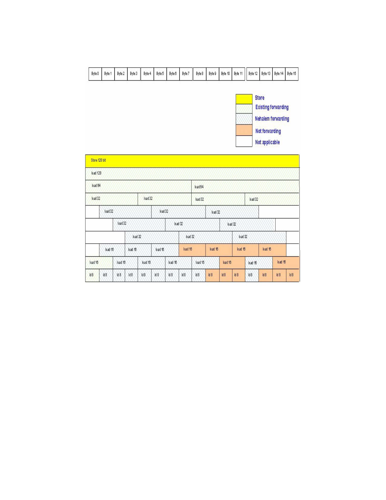
NEHALEM MICROARCHITECTURE
The store-forwarding situations for with respect to store operations of 16 bytes are illustrated in
Figure 4-3.
Figure 4-3. Store-Forwarding Scenarios of 16-Byte Store Operations
Nehalem microarchitecture allows store-to-load forwarding to proceed regardless of store address align-
ment (The white space in the diagram does not correspond to an applicable store-to-load scenario).
Figure 4-4 illustrates situations for store operation of 8 bytes or less.
Ref#: 248966-048
4-42
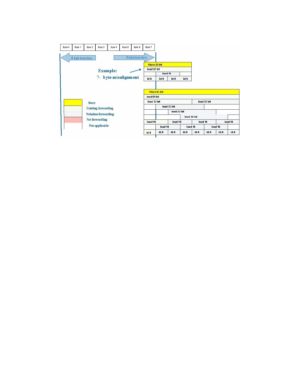
NEHALEM MICROARCHITECTURE
Figure 4-4. Store-Forwarding Enhancement in Nehalem Microarchitecture
4.4
REP STRING ENHANCEMENT
REP prefix in conjunction with MOVS/STOS instruction and a count value in ECX are frequently used to
implement library functions such as memcpy()/memset(). These are referred to as "REP string" instruc-
tions. Each iteration of these instruction can copy/write constant a value in byte/word/dword/qword
granularity The performance characteristics of using REP string can be attributed to two components:
startup overhead and data transfer throughput.
The two components of performance characteristics of REP String varies further depending on granu-
larity, alignment, and/or count values. Generally, MOVSB is used to handle very small chunks of data.
Therefore, processor implementation of REP MOVSB is optimized to handle ECX < 4. Using REP MOVSB
with ECX > 3 will achieve low data throughput due to not only byte-granular data transfer but also addi-
tional startup overhead. The latency for MOVSB, is 9 cycles if ECX < 4; otherwise REP MOVSB with ECX
>9 have a 50-cycle startup cost.
For REP string of larger granularity data transfer, as ECX value increases, the startup overhead of REP
String exhibit step-wise increase:
• Short string (ECX <= 12): the latency of REP MOVSW/MOVSD/MOVSQ is about 20 cycles.
• Fast string (ECX >= 76: excluding REP MOVSB): the processor implementation provides hardware
optimization by moving as many pieces of data in 16 bytes as possible. The latency of REP string
latency will vary if one of the 16-byte data transfer spans across cache line boundary:
— Split-free: the latency consists of a startup cost of about 40 cycles and each 64 bytes of data adds
4 cycles.
— Cache splits: the latency consists of a startup cost of about 35 cycles and each 64 bytes of data
adds 6cycles.
• Intermediate string lengths: the latency of REP MOVSW/MOVSD/MOVSQ has a startup cost of about
15 cycles plus one cycle for each iteration of the data movement in word/dword/qword.
Nehalem microarchitecture improves the performance of REP strings significantly over previous microar-
chitectures in several ways:
• Startup overhead have been reduced in most cases relative to previous microarchitecture.
• Data transfer throughput are improved over previous generation.
Ref#: 248966-048
4-43
NEHALEM MICROARCHITECTURE
• In order for REP string to operate in “fast string” mode, previous microarchitectures requires address
alignment. In Nehalem microarchitecture, REP string can operate in “fast string” mode even if the
address is not aligned to 16 bytes.
4.4.1
Enhancements for System Software
In addition to microarchitectural enhancements that can benefit both application-level and system-level
software, Nehalem microarchitecture enhances several operations that primarily benefit system soft-
ware.
Lock primitives: Synchronization primitives using the Lock prefix (e.g. XCHG, CMPXCHG8B) executes
with significantly reduced latency than previous microarchitectures.
VMM overhead improvements: VMX transitions between a Virtual Machine (VM) and its supervisor (the
VMM) can take thousands of cycle each time on previous microarchitectures. The latency of VMX transi-
tions has been reduced in processors based on Nehalem microarchitecture.
4.4.2
Efficiency Enhancements for Power Consumption
Nehalem microarchitecture is not only designed for high performance and power-efficient performance
under wide range of loading situations, it also features enhancement for low power consumption while
the system idles. Nehalem microarchitecture supports processor-specific C6 states, which have the
lowest leakage power consumption that OS can manage through ACPI and OS power management
mechanisms.
4.4.3
Intel® Hyper-Threading Technology (Intel® HT) Support in Nehalem
Microarchitecture
Nehalem microarchitecture supports Intel® Hyper-Threading Technology (Intel® HT). Its implementation
of Intel HT provides two logical processors sharing most execution/cache resources in each core. The HT
implementation in Nehalem microarchitecture differs from previous generations of HT implementations
using Intel NetBurst microarchitecture in several areas:
• Nehalem microarchitecture provides four-wide execution engine, more functional execution units
coupled to three issue ports capable of issuing computational operations.
• Nehalem microarchitecture supports integrated memory controller that can provide peak memory
bandwidth of up to 25.6 GB/sec in Intel Core i7 processor.
• Deeper buffering and enhanced resource sharing/partition policies:
— Replicated resource for HT operation: register state, renamed return stack buffer, large-page
ITLB.
— Partitioned resources for HT operation: load buffers, store buffers, re-order buffers, small-page
ITLB are statically allocated between two logical processors.
— Competitively-shared resource during HT operation: the reservation station, cache hierarchy, fill
buffers, both DTLB0 and STLB.
— Alternating during Intel HT operation: front end operation generally alternates between two
logical processors to ensure fairness.
— HT unaware resources: execution units.
Ref#: 248966-048
4-44
NEHALEM MICROARCHITECTURE
Ref#: 248966-048
4-45
NEHALEM MICROARCHITECTURE
Ref#: 248966-048
4-46
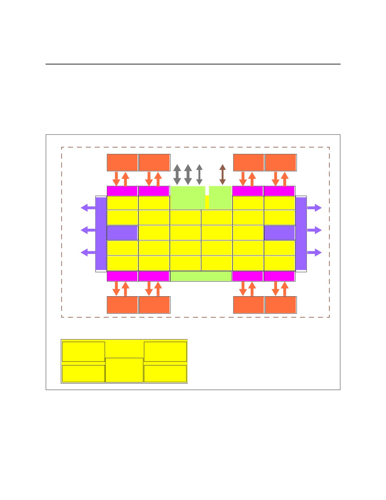
KNIGHTS LANDING MICROARCHITECTURE OPTIMIZATION
CHAPTER 5
KNIGHTS LANDING MICROARCHITECTURE OPTIMIZATION
Intel® Xeon PhiTM Processors 7200/5200/3200 Series are based on the Knights Landing microarchitec-
ture. Coding techniques for software targeting the Knights Landing microarchitecture are described in
this chapter. Processors based on the Knights Landing microarchitecture can be identified using CPUID’s
DisplayFamily_DisplayModel signature, which can be found in Table 2-1 of Chapter 2, “Intel® 64 and IA-
32 Processor Architectures” of Intel® 64 and IA-32 Architectures Software Developer’s Manual, Volume
4.
x 4
2 x 16
DM
x 4
MCDRAM
MCDRAM
MCDRAM
MCDRAM
EDC
EDC
EDC
EDC
PCIe
D
DMI
D
Gen 3
D
D
R
R
Multiple Tiles
C
C
H
H
DDR MC
Connected by
DDR MC
A
A
N
N
2-D Mesh
N
N
E
Interconnect
E
L
L
S
S
EDC
EDC
MISC
EDC
EDC
Physical
MCDRAM
MCDRAM
MCDRAM
MCDRAM
Package
Tile
CHA
2 VPU
2 VPU
1MB
Core
L 2
Core
Figure 5-1. Tile-Mesh Topology of the Knights Landing Microarchitecture
The Knights Landing microarchitecture is designed for processors and co-processor product families that
target highly-parallel, high-performance applications. An Intel Xeon Phi processor based on the Knights
Landing microarchitecture is comprised of:
• A large number of tiles.
• A two-dimensional mesh interconnect connecting the tiles.
Ref#: 248966-048
5-47
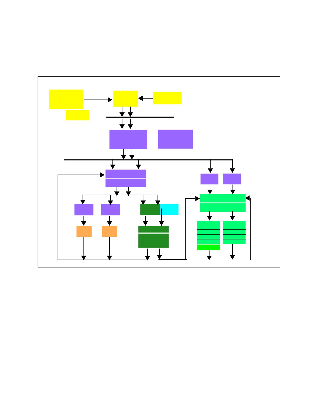
KNIGHTS LANDING MICROARCHITECTURE OPTIMIZATION
• An advanced memory sub-system supplying data to all the tiles containing IA-compatible processor
cores and cache hierarchy.
Figure 5-1 depicts a collection of “tile” units (or pairs of processor cores) connected by a two-dimensional
mesh network, offering I/O capabilities via PCIe and DMI interfaces, a memory sub-system supporting
high-bandwidth optimized MCDRAM, and capacity-optimized DDR memory channels.
Fetch &
branch
Instruction
predict
Decode
Cache
ITLB
Allocate
Retire
Rename
Integer Rename Buffer
FP
FP
RS
RS
Integer RF .
FP Rename Buffer
ALU
ALU
Recycle
MEM
FP Register File
RS
RS
RS .
Buffer.
Vec
ALU
Vec ALU
TLBs
ALU
ALU
VECINTMUL
L1 Data
Cache.
SHUFFLE
X87
Figure 5-2. Processor Core Pipeline Functionality of the Knights Landing Microarchitecture
Figure 5-1 also illustrates each tile comprising:
• Two out-of-order IA processor cores supporting Intel® Hyper-Threading Technology (Intel® HT)with
4 logical processors per core.
• A 1 MByte L2 cache shared between the two processor cores in the tile.
• A Caching Homing Agent (CHA) connecting each tile to the 2-D mesh interconnect.
• Each processor core also provides a dedicated vector processing unit (VPU) capable of executing 512-
bit, 256-bit, 128-bit and scalar SIMD instructions.
Figure 5-2 illustrates the microarchitectural pipelines of a processor core (including the VPU pipelines)
inside a tile.
The processor core in the Knights Landing microarchitecture provides the following features:
• An out-of-order (OOO) execution engine with 6-wide execution (2 VPU, 2 memory, 2 integer)
pipeline. Specifically, the out-of-order engine is supported by:
Ref#: 248966-048
5-48
KNIGHTS LANDING MICROARCHITECTURE OPTIMIZATION
— The front end can decode two instructions per-cycle into micro-ops (uops).
— The allocate/rename stage is also two-wide.
— The out-of-order engine has distributed reservation stations (72-entry deep) feeding the integer,
memory, and VPU pipelines.
• The VPU can execute Intel AVX-512F, Intel AVX-512CD, Intel AVX-512ER, Intel AVX-512PF, Intel AVX,
and 128-bit SIMD/FP instructions.
• The VPU can perform two 512-bit FMA operations per cycle; x87 and MMX instructions throughput is
limited to one per cycle.
• Each processor core supports 4 logical processors via Intel HT.
• Two processor cores share a 1 MByte L2 cache and form a tile.
5.1
FRONT END
The front end can fetch 16 bytes of instructions per cycle. The decoders can decode up to two instructions
of not more than 24 bytes in a cycle. The decoders can only provide a single uop per instruction. If an
instruction decodes into multiple uops (e.g., VSCATTER*), the microcode sequencer (MS) will supply the
uop flow with a performance bubble of three to seven cycles, depending on instruction alignment in the
decoder and length of the MS flow. The decoder will also have a small delay if a taken branch is encoun-
tered. If an instruction has more than three prefixes, there will be a multi-cycle bubble.
The front end is connected to the OOO execution engine through the Allocation, Renaming and Retire-
ment cluster. Scheduling of uops is handled with distributed reservation stations across the integer,
memory and VPU pipelines.
5.1.1
Out-of-Order Engine
The reorder buffer (ROB) is 72 uops deep. There are 16 store buffers (for both address and data).
Distributed scheduling of uops include (see Figure 5-2):
• Two integer reservation stations (one per dispatch port) are 12 entries each.
• The single MEC reservation station has 12 entries, and dispatches up to 2 uops per cycle.
• The two VPU reservation stations (one per dispatch port) are 20 entries each.
The reservation stations, ROB, and store data buffers are hard partitioned per logical processor
(depending on the processor core operating with one, two, or four active logical processors). Hard parti-
tioning of resources changes as logical processors wake up and go to sleep. The store address buffers
have two entries reserved per logical processor, with the remaining entries shared among the logical
processors.
Ref#: 248966-048
5-49