Intel 64 and IA-32 Architectures. Software Developer’s Manual (Collection, 2023) - page 152

KNIGHTS LANDING MICROARCHITECTURE OPTIMIZATION
The integer reservation stations can dispatch 2 uops per cycle each, and are able to do so out-of-order.
The memory execution reservation station dispatches 2 uops from its scheduler in-order, but uops can
complete in any order. The data cache can read two 64B cache lines and write one cache line per cycle.
The VPU reservation stations can dispatch 2 uops per cycle each and complete out-of-order.
The OOO engine in the Knights Landing microarchitecture is optimized to favor execution throughput
over latency. Loads to integer registers (e.g., RAX) are 4 cycles, and loads to VPU registers (e.g., XMM0,
YMM1, ZMM2, or MM0) are 5 cycles. Only one integer load is possible per cycle, but the other memory
operations (store address, vector load, and prefetch) can dispatch two per cycle. Stores commit post-
retirement, at a rate of 1 per cycle. The data cache and instruction caches are each 32 KB in size.
Most commonly-used integer math instructions (e.g. add, sub, cmp, test) have a throughput of 2 per
cycle with latency of a single cycle. The integer pipeline has only one integer multiplier with a latency of
3 or 5 cycles depending on the operand size. Latency of integer division will vary depending on the
operand size and input value; its throughput is expected to be not faster than one every ~20 cycles.
Store to load forwarding has a cost of 2 cycles and can forward one per cycle if the store-forwarding
restrictions are met.
Table 5-1. Integer Pipeline Characteristics of the Knights Landing Microarchitecture
Integer Instruction/operations
Latency (cycle)
Throughput ( cycles per instruction)
Simple Integer
1
0.5
Integer Multiply
3 or 5
1
Integer Divide
Varies
> 20
Store to Load Forward
2
1
Integer Loads
4
1
Many VPU math operations can dispatch on either VPU port with a latency of either 2 cycles or 6 cycles;
see Table 5-2. The following instructions can only dispatch on a single port:
• All x87 math operations.
• FP divisions and square roots.
• Intel AVX-512ER.
• Vector permute / shuffle operations.
• Vector to integer moves.
• Intel AVX-512CD conflict instructions.
• AESNI.
• The store data operation of a vector instruction with store semantics.
The above operations are limited to one of the two VPU dispatch pipes. Vector store data and vector to
integer moves are on one dispatch pipe. The remaining single pipe instructions are on the other dispatch
pipe.
Ref#: 248966-048
5-50

KNIGHTS LANDING MICROARCHITECTURE OPTIMIZATION
Table 5-2. Vector Pipeline Characteristics of the Knights Landing Microarchitecture
Vector Instructions
Latency (cycle)
Throughput (cycles per instruction)
Simple Integer
2
0.5
Most Vector Math (including FMA)
6
0.5
Mask Instructions (operating on opmask)
2
0.5
AVX-512ER (64-bit element)
7
2
AVX-512ER (32-bit element)
8
3
Vector Loads
5
0.5
Store to Load Forward
2
0.5
Gather (8 elements)
15
5
Gather (16 elements)
19
10
Register Move (GPR -> XMM/YMM/ZMM)
2
1
Register Move (XMM/YMM/ZMM -> GPR)
4
1
DIVSS/SQRTSS1
25
~20
DIVSD/SQRTSD1
40
~33
DIVP*/SQRTP*1
38
~10
Shuffle/Permute (1 source operand)1
2
1
Shuffle/Permute (2 source operands)1
3
2
Convert (from/to same width)1
2
1
Convert (from/to different width)1
6
5
Common x87/MMX Instructions1
6
1
NOTES:
1. The physical units executing these instructions may experience additional scheduling delay due to the physical layout of
the units in the VPU.
Additionally, some instructions in the Knights Landing microarchitecture will be decoded as one uop by
the front end but need to expand to two operations for execution. These complex uops will have an allo-
cation throughput of one per cycle. Examples of these instructions are:
• POP: integer load data + ESP update
• PUSH: integer store data + ESP update
• INC: add to register + update partial flags
• Gather: two VPU uops
• RET: JMP + ESP update
• CALL, DEC, LEA with 3 sources
Table 5-3 lists characteristics of the caching resources in the Knights Landing microarchitecture.
Ref#: 248966-048
5-51

KNIGHTS LANDING MICROARCHITECTURE OPTIMIZATION
Table 5-3. Characteristics of Caching Resources
Sets
Ways
Latency
Capacity/Comments
uTLB
8
8
1
64 4KB pages (fractured)1
DTLB (4KB page)
32
8
4
256 4KB pages
DTLB (2M/4M page)
16
8
4
128 2MB/4MB pages
DTLB (1GB page)
1
16
4
16 1GB pages
ITLB
1
48
4
48 4KB pages (fractured)
PDE
8
4
1
Page descriptors
L1 Data Cache
64
8
4 or 5
32 KB
Instruction Cache
64
8
4
32 KB
Shared L2 Cache
1024
16
13+L1 latency
1 MB
NOTES:
1. The uTLB and ITLB can only hold translations for 4 KB memory regions. If the relevant page is larger than 4 KB (such as
2MB or 1 GB), then the buffer holds the translation for the portion of the page that is being accessed. This smaller trans-
lation is referred to as a fractured page.
5.1.2
UnTile
In the Knights Landing microarchitecture, many tiles are connected by a mesh interconnect into a phys-
ical package; see Figure 5-1. The mesh and associated on-package components are referred to as
“untile”. At each mesh stop, there is a connection to the tile and a tag directory that identifies which L2
cache (if any) holds a particular cache line. There is no shared L3 cache within a physical package.
Memory accesses that miss in the tile must go over the mesh to the tag directory to identify any cached
copies in another tile. Cache coherence uses the MESIF protocol. If the cache line is not cached in another
tile, then a request goes to memory.
MCDRAM is an on-package, high bandwidth memory subsystem that provides peak bandwidth for read
traffic, but lower bandwidth for write traffic (compared to reads). The aggregate bandwidth provided by
MCDRAM is higher than the off-package memory subsystem (i.e., DDR memory). DDR memory band-
width can potentially be saturated by writes or reads alone. The achievable memory bandwidth for
MCDRAM is approximately 4x - 6x of what DDR can do, depending on the mix of read and write traffic.
MCDRAM capacity supported by the Knights Landing microarchitecture is either 8 or 16 GB, depending on
product-specific features. The peak MCDRAM bandwidth will vary according to the size of the installed
MCDRAM. MCDRAM has higher bandwidth but lower capacity than DDR. The Maximum DDR capacity is
384 GB for the Knights Landing microarchitecture.
The physical memory in a platform comprises both MCDRAM and DDR memory; they can be partitioned
in a number of different modes of operation. The commonly-used modes are summarized below.
• Cache mode: MCDRAM as a direct mapped cache and DDR is used as system memory addressable by
software.
• Flat mode: MCDRAM and DDR map to disjoint addressable, system memory.
• Hybrid mode: MCDRAM is partitioned; parts of MCDRAM act as direct mapped cache, the rest of
MCDRAM is directly addressable. DDR map to addressable system memory.
Ref#: 248966-048
5-52
KNIGHTS LANDING MICROARCHITECTURE OPTIMIZATION
The configuration between tiles, tag directories and the mesh support the following modes of clustering
operation for cache coherent traffic:
• All-to-All: the requesting core, tag directory and memory controller for a cache line can be anywhere
in the mesh.
• Quadrant: the tag directory and memory that it monitors are in the same quadrant of the mesh, but
the requesting core can be anywhere in the mesh.
• Sub-NUMA Clustering (SNC): In SNC mode, BIOS expose each quadrant as a NUMA node. This
requires software to recognize the NUMA domains and co-locate the requesting core, tag directory,
and memory controller in the same quadrant of the mesh to realize the benefit of optimal cache miss
latency.
If critical portions of an application working set fit in the capacity of MCDRAM, performance could benefit
greatly by allocating it into the MCDRAM and using flat or hybrid mode. Cache mode is generally best for
code that has not yet been optimized for the Knights Landing microarchitecture, and has a working set
that MCDRAM can cache.
In general, cache miss latency in All-to-All mode will be worse than it is in Quadrant mode; SNC mode
can achieve the best latency. Quadrant mode is the default mesh configuration. SNC clustering requires
some support from software to recognize the different NUMA nodes. If DDR is not populated evenly (e.g.,
missing DIMMs), the mesh will need to use the All-to-All clustering mode.
When multiple tiles read the same cache line, each tile might have a copy of the cache line. If both cores
in the same tile read a cache line, there will only be a single copy in the L2 cache of that tile.
If MCDRAM is configured as a cache, it can hold data or instructions accessed by the cores in a single
place. If multiple tiles request the same line, only one MCDRAM cacheline will be used.
L1 data cache has higher bandwidth and lower latency than L2 cache. Cache line access from L2 has
higher bandwidth and lower latency than access from memory.
MCDRAM and DDR memory have different latency and throughput profiles. This becomes important
when choosing between cache vs. flat or other memory modes. In most memory configurations, the DDR
capacity will be substantially larger than MCDRAM capacity. Likewise, MCDRAM capacity should be much
larger than the combined L2 cache.
Working sets that fit in MCDRAM capacity, but not in the L2 cache, should be in MCDRAM. Large or rarely
accessed structures should migrate to DDR. In Knights Landing microarchitecture, hardware will try to do
this dynamically if MCDRAM is put in cache or hybrid memory modes. If memory is in the flat memory
mode, data structures are bound to one memory or the other (MCDRAM or DDR) at allocation time. The
programmer should strive to maximize the number of memory access that go to MCDRAM. One possible
algorithm would allocate data structures into MCDRAM if they are frequently accessed, and have working
sets that do not fit into the tile caches.
In cache memory mode, the MCDRAM access is done first. If the cacheline is not in MCDRAM, the DDR
access begins. Because of this, the perceived memory access latency of DDR in cache memory mode is
higher than in flat memory mode.
5.2
INTEL® AVX-512 CODING RECOMMENDATIONS FOR KNIGHTS
LANDING MICROARCHITECTURE
The Intel AVX-512 family comprises a collection of instruction set extensions. For an overview and de-
tailed features (EVEX prefix encoding, opmask support, etc.) of the Intel AVX-512 family of instruc-
tions, see the Intel® 64 and IA-32 Architectures Software Developer’s Manual, Volume 1. Intel Xeon
Phi processors (7200, 5200, 3100 series) based on the Knights Landing microarchitecture support AVX-
512 Foundation (AVX-512F), AVX-512 Exponential and Reciprocal (AVX-512ER), AVX-512 Conflict
(AVX-512CD), and AVX-512 Prefetch extensions. Intel AVX and Intel AVX2 instructions are also sup-
ported on processors based on the Knights Landing microarchitecture. Prior generation Intel Xeon Phi
processors (7100, 5100, 3100 series) do not support Intel AVX-512, Intel AVX2, nor Intel AVX instruc-
tions.
Ref#: 248966-048
5-53

KNIGHTS LANDING MICROARCHITECTURE OPTIMIZATION
5.2.1
Using Gather and Scatter Instructions
Gather instructions in Intel AVX-512F are enhanced over those in Intel AVX2, performing 512-bit opera-
tions (either 16 elements of 32-bit data or 8 elements of 64-bit data) and using an opmask register as
writemask for conditional updates of fetched elements to the destination ZMM register.
Scatter instructions in Intel AVX-512F selectively store elements in a ZMM register to memory locations
expressed via an index vector. Conditional store to the destination location is selected using an opmask
register. Scatter instructions are not supported in Intel AVX or Intel AVX2.
Consider the following C code fragment:
for (uint32 i = 0; i < 16; i ++) {
b[i] = a[indirect[i]];
// vector compute sequence
}
Example 5-1. Gather Comparison Between Intel® AVX-512F and Intel® AVX2
AVX-512F
AVX2
vmovdqu zmm0, [rsp+0x1000] ; load indirect[]
vmovdqu ymm0, [rsp+0x1000] ; load half of index vector
kxnor k1,k0, k0; prepare mask
vmovdqu ymm3, [rsp+0x1020] ; 2nd half of indirect[]
vpgatherdd zmm2{k1}, [rax+zmm0*4]
vpcmpeqdd ymm4, ymm4, ymm4 ; prepare mask
; compute sequence using vector register
vmovdqa ymm1, ymm4
vpgatherdd ymm2, [rax+ymm0*4], ymm1
vpgatherdd ymm5, [rax+ymm3*4], ymm4
; compute sequence using vector register
When using VGATHER and VSCATTER, you often need to set a mask to all ones. An efficient instruction to
do this is KXNOR of a mask register with itself. Since VSCATTER and VGATHER clear their mask as the last
thing they do, a loop carried dependence from the VGATHER to KXNOR can be generated. Because of
this, it is wise to avoid using the same mask for source and destination in KXNOR. Since it is rare for the
k0 mask to be used as a destination, it is likely that “KXNORW k1, k0, k0” will be faster than “KXNOR k1,
k1, k1”.
Gather and Scatter instructions in AVX-512F are different from those in prior generation Intel Xeon Phi
processors (abbreviated by “Previous Generation” in Example 5-2).
Example 5-2. Gather Comparison Between Intel® AVX-512F and Previous Generation Equivalent
AVX-512F
Previous Generation Equivalent Sequence
vmovdqu zmm0, [rsp+0x1000] ; load indirect[]
vmovdqu zmm0, [rsp+0x1000] ; load indirect[]
kxnor k1,k0, k0; prepare mask
kxnor
k1,k1 ; prepare mask
vpgatherdd zmm2{k1}, [rax+zmm0*4]
g_loop:
; verify gathered elements are complete
; compute sequence using vector register
vpgatherdd zmm2{k1}, [rax+zmm0*4]
jknzd
k1, g_loop ; gather latency exposure
; compute sequence using vector register
5.2.2
Using Enhanced Reciprocal Instructions
The Intel AVX-512ER instructions provide high precision approximations of exponential, reciprocal, and
reciprocal square root functions. The approximate math instructions in Intel AVX-512ER provide 28 bits
of accuracy, compared to 11 bits in RCPSS or 14 bits with VRCP14SS. Intel AVX-512ER can reduce execu-
tion time for iterative algorithms like Newton-Raphson. Example 5-3 contains sample code using the
Newton-Raphson algorithm to compute a single 32b float division with VRCP28SS. Both values are read
off the stack. Note the use of rounding mode overrides on some of the math operations.
Ref#: 248966-048
5-54

KNIGHTS LANDING MICROARCHITECTURE OPTIMIZATION
Example 5-3. Using VRCP28SS for 32-bit Floating-Point Division
vgetmantss xmm18, xmm18, [rsp+0x10], 0
vgetmantss xmm20, xmm20, [rsp+0x8], 0
vrcp28ss
xmm19, xmm18, xmm18
vgetexpss
xmm16, xmm16, [rsp+0x8]
vgetexpss
xmm17, xmm17, [rsp+0x10]
vsubss
xmm22, xmm16, xmm17
vmulss
xmm21{rne-sae}, xmm19, xmm20
vfnmadd231ss xmm20{rne-sae}, xmm21, xmm18
vfmadd231ss xmm21, xmm19, xmm20
vscalefss
xmm0, xmm21, xmm22
5.3
USING AVX-512CD INSTRUCTIONS
Refer to Section 18.16, “Conflict Detection” for details on using the Intel AVX-512 Conflict Detection
instructions.
5.3.1
Using Intel® Hyper-Threading Technology (Intel® HT)
The Knights Landing microarchitecture supports 4 logical processors with each processor core. There are
choices that highly-threaded software may need to consider with respect to:
• Maximizing per-thread performance by providing maximum per-core resources to one logical
processor per core.
• Maximizing per-core throughput by allowing multiple logical processors to execute on a processor
core.
As thread count per core grows to 2 or 4, some applications will have higher per core performance, but
lower per thread performance. If an application can perfectly scale its performance to an arbitrary
number of threads, 4 threads per core is likely to have the highest instruction throughput. Practical
limitations on memory capacity or parallelism may limit the number of threads per core.
In Knights Landing microarchitecture, some per core resources (like the ROB or scheduler) are parti-
tioned to one for each of 4 logical processors. Because of this, a 3 thread configuration will have fewer
aggregate resources available than 1, 2, or 4 threads per core. Placing 3 threads on a processor core is
unlikely to perform better than 2 or 4 threads per core.
5.3.2
Front End Considerations
To ensure front end restrictions are not typically a performance limiter, software should consider the
following:
• MSROM instructions should be avoided if possible. A good example is the memory form of CALL near
indirect. It will often be better to perform a load into a register and then perform the register version
of CALL. Additional examples are shown in Table 5-4.
• The total length of the instruction bytes that can be decoded each cycle is at most 16 bytes per cycle
with instructions not more than 8 bytes in length. For instruction length exceeding 8 bytes, only one
instruction per cycle is decoded on decoder 0. Vector instructions which address memory using 32-bit
displacement can cause the decoder to limit performance.
• Instructions with multiple prefixes can restrict decode throughput. The restriction is on the length of
bytes combining prefixes and escape bytes. There is a 3 cycle penalty when the escape/prefix count
Ref#: 248966-048
5-55

KNIGHTS LANDING MICROARCHITECTURE OPTIMIZATION
exceeds 3 with the Knights Landing microarchitecture. Only decoder 0 can decode an instruction
exceeding the limit of a prefix/escape byte restriction.
• Maximum number of branches that can be decoded each cycle is 1.
5.3.3
Instruction Decoder
Some IA instructions require a lookup in the microcode sequencer ROM (MSROM) to decode into a
multiple uop flow. Choosing an alternative sequence of instructions which does not require MSROM will
improve performance.
Table 5-4 provides alternate non-MSROM instruction sequences that can replace an instruction that
decodes from MSROM.
Table 5-4. Alternatives to MSROM Instructions
Instruction from MSROM
Recommendation for Knights Landing
CALL m16/m32/m64
Load + CALL reg
PUSH m16/m32/m64
Store + RSP update
(I)MUL r/m16 (Result DX:AX)
Use (I)MUL r16, r/m16 if extended precision not required, or (I)MUL r32, r/m32
(I)MUL r/m32 (Result EDX:EAX)
Use (I)MUL r32, r/m32 if extended precision not required, or (I)MUL r64, r/m64
(I)MUL r/m64 (Result RDX:RAX)
Use (I)MUL r64, r/m64 if extended precision not required
5.3.4
Branching Indirectly Across a 4GB Boundary
Another important performance consideration from a front end standpoint is branch prediction for indi-
rect branches (indirect branch or call, or ret). For 64-bit applications, indirect branch prediction fails
when the target of a branch is in a different 4GB chunk of the address space from the source. (I.e. the
top 32 bits of the virtual addresses of the source and target are different). This is more likely to happen
when the application is split into shared libraries. Developers can build statically to improve the locality
in their code, particularly for latency-sensitive library calls that are accessed frequently. Another option
is to use glibc 2.23 or later, and set the LD_PREFER_MAP_32BIT_EXEC environment variable which
requests that the dynamic linker place all shared libraries at the bottom of the address space.
5.4
INTEGER EXECUTION CONSIDERATIONS
5.4.1
Flags usage
Many instructions have an implicit data result that is captured in a flags register. These results can be
consumed by a variety of instructions such as conditional moves (cmovs), branches, and even a variety
of logic/arithmetic operations (such as rcl). The most common instructions used in computing branch
conditions are compare instructions (CMP). Branches dependent on the CMP instruction can execute in
the next cycle. The same is true for branch instructions dependent on ADD or SUB instructions.
INC and DEC instructions require an additional uop to merge the flags as they are partial flag writers. As
a result, an INC or a DEC instruction should be replaced by “ADD reg, 1” or “SUB reg, 1” to avoid a partial
flag penalty.
Instructions that operate on 8-bit or 16-bit registers are not optimized in hardware in the Knights
Landing microarchitecture. In general, it is faster to use integer instructions operating on 32-bit or 64-bit
general purpose registers than 8-bit or 16-bit registers.
Ref#: 248966-048
5-56

KNIGHTS LANDING MICROARCHITECTURE OPTIMIZATION
5.4.2
Integer Division
Integer division can be a common operation in some mathematical expressions. However, using hard-
ware integer divide instructions is often less than optimal in performance. If the divisor is known to be
relatively small (16 bits or less), there are fast SW sequences to emulate the division. If the divisor is
known to be a power of 2, use SHR (division) and/or AND (remainder) instead of DIV. Division by a
constant can be replaced by MUL with a constant. If the input values are highly constrained, a pre-
computed lookup table is likely to provide better performance. Some examples of the techniques can be
found in Section 13.2.4, “Replace 128-bit Integer Division with 128-bit Multiplication,” and Section 14.5,
“Numerical Data Conversion to ASCII Format.”
Division instructions should be aggressively minimized by the compiler, either using the techniques
mentioned earlier, or by hoisting redundant divisions out of inner loops.
5.5
OPTIMIZING FP AND VECTOR EXECUTION
5.5.1
Instruction Selection Considerations
In general, using 512-bit instructions are more favorable to achieve higher throughput than 256-bit
instructions. The same applies relative to 256-bit vs. 128-bit vector instructions. 128-bit SSE instructions
are likely to achieve higher throughput than using X87 instruction equivalents. Often, X87 instruction
functionality (transcendental) not present in vector instruction extensions natively can be replaced by
library implementations using vector instructions.
In the Knights Landing microarchitecture, COMIS* and UCOMIS* instructions (legacy, VEX, or EVEX
encoding) that update EFLAGS are slow. These should be replaced by a more optimal sequence of the
Intel AVX-512F version of VCMPS* and KORTEST.
Example 5-4. Replace VCOMIS* with VCMPSS/KORTEST
vcmpss k1, xmm1, xmm2, imm8 ; specify imm8 according to desired primitive
kortest k1, k1
Some instructions, like VCOMPRESS*, are single uop when writing a register, but an MS flow when
writing memory. Where possible, it is much better to do a VCOMPRESS to register and then store it.
Similar optimizations apply to all vector instructions that do some sort of operation followed by a store
(e.g., PEXTRACT).
In the Knights Landing microarchitecture, mixing SSE instructions and Intel AVX instructions require a
different set of considerations to avoid loss of performance due to intermixing of SSE and Intel AVX
instructions. Replace SSE code with AVX-128 equivalents, whenever possible.
Situations that can result in a performance penalty are:
• If an Intel AVX instruction encoded with a vector length of more than 128 bits is allocated before the
retirement of previous in-flight SSE instructions.
• VZEROUPPER instruction throughput is slow, and is not recommended to preface a transition to AVX
code after SEE code execution. The throughput of VZEROALL is also slow. Using either the
VZEROUPPER or the VZEROALL instruction is likely to result in performance loss.
Conditional packed load/store instructions, like MASKMOVDQU and VMASKMOV, use a vector register for
element selection. AVX-512F instructions provide alternatives using an opmask register for element
selection and are preferred over using a vector register for element selection.
Some vector math instructions require multiple uops to implement in the VPU. This increases the latency
of the individual instruction beyond the standard math latencies of 2 and 6. In general, instructions that
alter output/input element width (e.g., VCVTSD2SI) fall into this category. Many Intel AVX2 instructions
Ref#: 248966-048
5-57

KNIGHTS LANDING MICROARCHITECTURE OPTIMIZATION
that operate on byte and word quantities have reduced performance compared to the equivalents that
operate on 32b or 64b quantities.
Some execution units in the VPU may incur scheduling delay if a sequence of dependent uop flow needs
to use these execution units. When this happens, it will have an additional cost of a 2-cycle bubble. Code
that frequently transition between the outlier units with other units in the VPU can experience a perfor-
mance issue due to these bubbles.
Most of the Intel AVX-512 instructions support using an opmask register to make conditional updates to
the destination. In general, using an opmask with all 1’s will be the fastest relative to using an opmask
with other non-zero values. Using a non-zero opmask value, the instruction will be similar in speed rela-
tive to an opmask with all 1s, if zeroing-the-non-updated element is selected. Using a non-zero opmask
value with merging (preserving) non-updated elements of the destination will likely be slower.
Horizontal add/subtraction instructions in Intel AVX2 do not have promoted equivalents in Intel AVX-512.
Horizontal reduction is best implemented using software sequences; see Example E-5.
In situations where an algorithm needs to perform reduction, reduction can often be implemented
without horizontal addition.
Example E-6 shows code fragment for the inner loop of a DGEMM matrix multiplication routine, which
computes the dense matrix operation of C = A * B.
In Example E-6, there are 16 partial sums. The sequence of FMA instructions make use of the two VPU
capability of 2 FMAs per cycle throughput, 6 cycles latency. The FMA code snippet in Example E-6 is
presented using uncompressed addressing form for the memory operand. It is important for code gener-
ators to ensure optimal code generation will make use of compressed disp8 addressing form, so that the
length of each FMA instruction will be less than 8 bytes. At the end of the inner loop, the partial sums will
need to be aggregated and store the result matrix C to memory.
Example E-5. Using Software Sequence for Horizontal Reduction
vextractf64x4 ymm1, zmm6, 1; reduction of 16
vextractf64x4 ymm1, zmm6, 1; reduction of 8
elements
elements
vaddps ymm1, ymm6, ymm1
vaddps ymm1, ymm6, ymm1
vpermpd ymm4, ymm1,0xff
valignq ymm4, ymm1,0x3
vpermpd ymm5, ymm1,0xaa
valignq ymm5, ymm1,0x2
vpermpd ymm3, ymm1,0x44
valignq ymm3, ymm1,0x1
vaddps
xmm1, xmm1, xmm4
vaddsd ymm1, ymm1, ymm4
vaddps
xmm3, xmm5, xmm3
vaddsd ymm3, ymm5, ymm3
vaddps
xmm3, xmm1, xmm3
vaddsd ymm3, ymm1, ymm3
vpsrlq xmm1, xmm3, 32
vaddss xmm3, xmm1, xmm3
Ref#: 248966-048
5-58

KNIGHTS LANDING MICROARCHITECTURE OPTIMIZATION
Example E-6. Optimized Inner Loop of DGEMM for Knights Landing Microarchitecture
;; matrix - matrix dense multiplication
prefetcht0 [rdi+0x400] ;; get A matrix element into L1$
vmovapd zmm30, [rdi]
prefetcht0 [rsi+0x400] ;; get B matrix element into L1$
vfmadd231pd zmm1, zmm30, [rsi+r12]{b} ;; broadcast B elements
vfmadd231pd zmm2, zmm30, [rsi+r12+0x08]{b} ;; displacement shown in un-compressed form
vfmadd231pd zmm3, zmm30, [rsi+r12+0x10]{b}
vfmadd231pd zmm4, zmm30, [rsi+r12+0x18]{b}
vfmadd231pd zmm5, zmm30, [rsi+r12+0x20]{b}
vfmadd231pd zmm6, zmm30, [rsi+r12+0x28]{b}
vfmadd231pd zmm7, zmm30, [rsi+r12+0x30]{b}
vfmadd231pd zmm8, zmm30, [rsi+r12+0x38]{b}
prefetcht0 [rsi+0x440]
;; pull line into the L1$
vfmadd231pd zmm9, zmm30, [rsi+r12+0x40]{b}
vfmadd231pd zmm10, zmm30, [rsi+r12+0x48]{b}
vfmadd231pd zmm11, zmm30, [rsi+r12+0x50]{b}
vfmadd231pd zmm12, zmm30, [rsi+r12+0x58]{b}
vfmadd231pd zmm13, zmm30, [rsi+r12+0x60]{b}
vfmadd231pd zmm14, zmm30, [rsi+r12+0x68]{b}
vfmadd231pd zmm15, zmm30, [rsi+r12+0x70]{b}
vfmadd231pd zmm16, zmm30, [rsi+r12+0x78]{b}
5.5.2
Porting Intrinsics from Previous Generation
Most intrinsics map to individual instructions of the native hardware. Some 512-bit intrinsics may provide
syntax that hides the difference between AVX-512F and the 512-bit incompatible previous generation
instruction set.
However, intrinsic code that is optimized to run on previous generations will likely not run optimized on
the Knights Landing microarchitecture, due to differences in the underlying microarchitecture (e.g.,
unaligned memory access, cost differences of permutes, limitations of previous generations).
It is likely that coding an algorithm in a high level language (C/Fortran) to compile with Intel Compilers
supporting Intel AVX-512F will generate more optimal code than using previous generation intrinsics.
5.5.3
Vectorization Trade-Off Estimation
Profitability of vectorization of loops written in a high-level language to use AVX-512 is an important part
of optimization for compilers as well as for hand coding assembly. Estimating this for the simplest type of
loop construct can be based on trip count alone. For example, a trip count of 4 or less may be difficult to
realize performance gain over scalar code. With Intel AVX-512, a trip count of 16 may be the minimum
to consider vectorization.
Estimation of vectorization trade-off for more elaborate loop construct requires more sophistication. The
rest of this section provides an analytic approach of examining the composition within the loop body and
makes use of a table of cost estimates of basic operations, Table 5-5,to derive the trade-off comparison
between vectorization versus scalar code.
Ref#: 248966-048
5-59

KNIGHTS LANDING MICROARCHITECTURE OPTIMIZATION
Table 5-5. Cycle Cost Building Blocks for Vectorization Estimate for Knights Landing Microarchitecture
Operation
Cost (cycles)
Example Code Construct
Simple scalar math
1
A*B+C, or A+B, or A*B
Load (split cacheline)
1 (2)
A[i] /* load reference to an array element */
Store (split cacheline)
1(2)
A[i] = 2;
Gather (Scatter) 8 elements
15 (20)
A[key[i]]
Gather (Scatter) 16elements
20 (25)
A[key[i]] ;
Horizontal reduction
30
sum += A[i]
Division or Square root
15
A/B
To illustrate the cost build-up approach, consider the simple loop:
for (i=0; i<N; i++) { sum += a[i]*K + b[i]; }
Within the loop body, the basic operations consist of:
• Two loads (a[i], b[i]) per iteration.
• An FMA per iteration.
• For scalar version: an accumulate per loop iteration; for vectorization: a horizontal reduction at the
end of the loop.
The total cost of N trips for scalar code is 4N. By comparison, the total cost for vectorized code using AVX-
512 on a 64-bit data element would be 3 * Ceiling(N/8) + 30, assuming both the main loop and
remainder loop (if N is not multiples of 8) are vectorized. Therefore, profitable vectorization will need a
trip count of at least 9.
Consider another example involving fetching data from irregular access patterns which might take
advantage of GATHER instructions:
for (i=0; i<N; i++) {c[i] = a[indir[i]] * K + b[i]; }
Within the loop body, the basic operations consist of:
• Two loads (indir[i], b[i]) per iteration.
• An FMA per iteration.
• A store per iteration.
• For scalar version: a 3rd load per loop iteration; for vectorization: one GATHER per 8 iteration.
The total cost of N trips for scalar code is 5N. By comparison, the total cost for vectorized code would be
19* Ceiling(N/8). Scalar would be faster if N < 4.
Ref#: 248966-048
5-60
KNIGHTS LANDING MICROARCHITECTURE OPTIMIZATION
Consider an example involving fetching data from twice irregular access patterns than the previous
example:
for (i=0; i<N; i++) {c[i] = a[ind[i]]*K + b[ind[i]]; }
• One load (ind[i]) per iteration.
• An FMA per iteration.
• A store per iteration.
• For scalar version: two more loads per loop iteration; for vectorization: two GATHERs per 8 iteration.
The total cost of N trips for scalar code is still 5N. By comparison, the total cost for vectorized code would
be (15*2 + 3)* Ceiling(N/8) = 33* Ceiling(N/8). Even a relatively small profitability of vectorization will
require a significantly larger trip count.
Consider the next example involving fetching data from one irregular access pattern and horizontal
reduction:
for (i=0; i<N; i++) {sum += a[ind[i]]*K + b[i]; }
Scalar cost is still 5N. Cost of vectorization is now 19*Ceiling(N/8) + 30. Scalar code would be faster for
N <= 13.
Consider an example of scatter with division:
for (i=0; i<N; i++) {c[ind[i]] = a[i] / b[i]; }
The scalar cost is (15+4)*N. Cost of vectorization would be (15+20+3)*Ceiling(N/8). Vectorization
would be profitable for N > 2.
In the case of gather followed by scatter:
for (i=0; i<N; i++) {b[ind[i]] = a[ind[i]]; }
The cost of scalar code is 3*N, and vector code will cost (15+20+1)*Ceiling(N/8). Vectorization will not
be profitable.
Ref#: 248966-048
5-61
KNIGHTS LANDING MICROARCHITECTURE OPTIMIZATION
For a loop body that is more complex, consider the code below from a workload known as miniMD:
for (int k = 0; k < numneigh; k++) {
int j = neighs[k];
double rsq = (xtmp - x[3*j])^2 +
(ytmp - x[3*j+1])^2 +
(ztmp - x[3*j+2])^2;
if (rsq < cutforcesq) {
double sr2 = 1.0/rsq;
double sr6 = sr2*sr2*sr2;
double force = sr6*(sr6-0.5)*sr2;
res1 += delx*force;
res2 += dely*force;
res3 += delz*force;
}
}
Before considering the IF clause, there is one load, 3 gathers (strided loads of x[]), 3 subtractions and 3
multiplies. Inside the IF clause, there is one division, 8 math operations, and 3 horizontal reductions. The
scalar cost is 10*numneigh + 23 * numneigh * percent_rsq_less_than_cutforcesq. The vector cost is
(52+23) * Ceiling(numneigh / 8) + 3 * 30. Scalar code makes sense if numneigh < 6 or if the compiler
is highly confident that the if clause is almost never taken.
For many compilers, a vectorized loop is generated, and a remainder loop is used to take care of the rest
of the operations. In other words, the vectorized loop is executed floor(N/8) times, and the remainder
loop is executed N mod 8 times. In that case, modify the equations above to use floor instead of ceiling
to determine whether the primary loop should be vectorized. For the remainder loop, the maximum value
of the loop trip count is known. If N is unknown, it is simplest to set N to half the maximum value (4 for
a ZMM vector of doubles).
More sophisticated analysis is possible. For example, the building block simple math operation of 1-cycle
cost in Table 5-5 covers common instruction sequences that are not blocked by a dependency chain or
long latency operations. Expanding entries of the cost table can cover more complex situations.
5.6
MEMORY OPTIMIZATION
5.6.1
Data Alignment
Data access to address spanning a cache line boundary will experience a small performance hit. Access
patterns that stream through memory can avoid cache line splits to make sure each 64-byte access is
aligned to a cache line boundary. When loading 32-bytes of memory to YMM, do not access 64-bytes of
memory with an opmask value to mask off the high 32 bytes.
Memory references crossing a 4-Kbytes boundary will incur significant cost in performance. Access
patterns that stream throughput memory using 512-bit instructions have a higher rate of crossing a 4-
KBytes boundary. So alignment to 64 byte will also avoid the penalty of a page split.
If possible to predict the distance in code space of the next crossing of page boundary, it can be helpful
to insert a PREFETCHT1 (to L2) a few iterations ahead of the current read stream. This can also start the
page translation early and permit the L2 hardware prefetcher to start fetching on the next page.
Some access patterns which might intend to use gather and scatter will always have pairs of consecutive
addresses. One common example is complex numbers, where the real and imaginary parts are laid out
Ref#: 248966-048
5-62
KNIGHTS LANDING MICROARCHITECTURE OPTIMIZATION
contiguously. It is also common when w, x, y, and z information is contiguous. If the values are 32b, it is
faster to gather and scatter the 32-bit elements as half as many 64-bit elements. If the numbers are 64
bits, then it is usually faster to load and insert a 128-bit element instead of gathering 64-bit elements.
5.6.2
Hardware Prefetcher
There are two types of HW prefetchers in a tile. The Instruction Pointer Prefetcher (IPP) resides in a
processor core and analyzes all the accesses in the data cache and the instructions that generated the
access. The prefetcher will then attempt to insert HW prefetches to the L1 cache if a strided access
pattern is detected on a cacheable page. The IPP will not cross a 4k page boundary. The IPP uses the
instruction address and logical processor to index into a table. For this reason, the compiler may insert
NOPs into large loops (>256 B) to make instructions that access memory go into different table entries.
The L2 HW prefetcher tries to identify streaming access patterns, and can track up to 48 access patterns.
A streaming access pattern touches consecutive cache lines in increasing or decreasing order - the stride
detected in the L2 is always +/-1 cacheline. The 48 detectors are allocated independently of the logical
processor that originated the request. Each detector looks at the accesses done within a 4 KB region. If
a stream is detected, HW prefetches for later elements of the stream will be sent to the L2 cache, and if
they miss, to memory. The HW prefetcher will not stream across a 4 KB boundary. If multiple access
patterns are done within the same 4 KB region, the detector can get confused, and fail to detect the
stream.
5.6.3
Software Prefetch
Knights Landing microarchitecture supports out-of-order execution. In general, it can hide cache miss
latency better than previous generation in-order microarchitecture. Hence, programmers should not use
the same aggressive approach to insert software prefetches.
With the two hardware prefetchers described in Section 5.6.2, most streaming and short stride access
patterns should be detected by the hardware prefetchers. If the access pattern is streaming, a
programmer might benefit from adding software prefetches beyond the current 4-KBytes page. If the
access pattern is known, but non-streaming, software prefetches can be beneficial in some situations.
This is especially true if the access pattern is a relatively large stride (>256 bytes), since the IPP will not
fetch across a 4 KB boundary. The software prefetch will do the PMH walk to fill the TLB, and to start the
memory reference early.
Generally, software prefetching into the L2 will show more benefit than L1 prefetches. A software
prefetch into L1 will consume critical hardware resources (fill buffer) until the cacheline fill completes. A
software prefetch into L2 does not hold those resources, and it is less likely to have a negative perfor-
mance impact. If you do use L1 software prefetches, it is best if the software prefetch is serviced by hits
in the L2 cache, so the length of time that the hardware resources are held is minimized.
Software prefetch instructions that are dropped will have a negative performance impact due to
consuming retirement slots from an invalid address. The performance penalty of prefetching an invalid
address or requiring OS privilege from user code can be very large. The performance monitoring event
NUKE.ALL provides an indication of when this might be affecting your code.
5.6.4
Memory Execution Cluster
The MEC has limited capability in executing uops out-of-order. Specifically, memory uops are dispatched
from the scheduler in-order, but can complete in any order. By re-arranging the order of memory instruc-
tions, performance may be improved if they make good use of the MEC’s capability.
Example 5-7 illustrates the effect of ordering the sequence of memory instructions of two read streams
accessing two arrays, a[] and b[]. The left side of Example 5-7 is the optimal sequence with the 2nd
vector load from b[] dispatched on cycle N+5, assuming an L1 cache hit. The right side of Example 5-7 is
a naive ordering of the memory instructions, resulting in the second vector load dispatched on cycle N+8.
Ref#: 248966-048
5-63

KNIGHTS LANDING MICROARCHITECTURE OPTIMIZATION
The right side sequence uses one more register than the left side. If the pointer loads would miss L1, the
benefit of left side will be greater than what is shown in the comment.
Example 5-7. Ordering of Memory Instruction for MEC
movq
r15, [rsp+0x40] ; cycle N (load &a[0])
movq
r15, [rsp+0x40] ; cycle N (load &a[0])
movq
r14, [rsp+0x48] ; cycle N+1 (load &b[0])
vmovups
zmm1, [r15+rax*8] ; executes in cycle N+4
vmovups
zmm1, [r15+rax*8] ; executes in cycle N+4
movq
r15, [rsp+0x48] ; cycle N+4 (load &b[0])
vmovups
zmm2, [r14+rax*8] ; cycle N+5
vmovups zmm2, [r15+rax*8] ; cycle N+8
If there are many loads in the machine, it might be possible to hoist up the pointer loads, so that there
are several memory references between the pointer load and de-reference, without requiring more
integer registers to be reserved.
5.6.5
Store Forwarding
Store forwarding restriction for integer execution and the MEC in the Knights Landing microarchitecture
is similar to those of the Silvermont microarchitecture. The following paragraphs describes the
forwarding restrictions with the VPU.
Vector, X87, and MMX loads and stores can forward (ZMM0, YMM1, XMM2, MM3, and ST4) if the stores
and loads have the same memory address and the load is not larger than the store. VPU stores cannot
forward to integer loads, and integer stores cannot forward to VPU loads. In either case, the load must
wait until the store is post-retirement to get the value from memory.
Vector stores that use an opmask cannot be forwarded from. If your algorithm requires such behavior,
you may benefit if you merge the value in a register, and then store to memory without a conditional
opmask. Later loads can then forward from the merged value.
5.6.6
Way, Set Conflicts
The memory hierarchy determines forwarding requirements based on the address of the access. The L1
data cache uses address bits 11:6 to identify which cache set to use. Forwarding logic uses bits 11:0 and
the size of the access to identify potential forwarding or conflicts between loads and stores. If there are
many conflicts, performance could be degraded.
Many dynamic memory allocation routines (may vary by OS and compiler) will start large memory
regions with the same pattern in the least significant 12 bits. If your access patterns touch many arrays
with identical shapes (element size and dimensions) and similar indices, performance could degrade
significantly due to set conflict. To void these set conflicts, it is beneficial for bits [11..6] of memory
accesses to be different. For example, consider:
a = malloc(sizeof(double) * 10000);
b = malloc(sizeof(double) * 10000);
for (i=0; i < 10000; i++) {
a[i] = b[i] + 0.5 * b[i-1]);
}
Very likely, in most OSes, the effective address of a[] and b[] will have identical lowest 12 bits, i.e., (a &
0xfff) == (b & 0xfff). Some intra-loop conflict may occur with:
• a[i] and b[i] of iteration N collide.
• a[i] of iteration N-1 and b[i-1] of iteration N collide.
Ref#: 248966-048
5-64
KNIGHTS LANDING MICROARCHITECTURE OPTIMIZATION
There are multiple ways to offset dynamic arrays. Examples include:
• Offset the working base pointer from the malloc result by an amount of several cache lines,
• Use customized malloc() routine,
• Use posix_memalign() routine with alignment directives for each dynamic allocation to have different
alignments (powers of 2 bytes: 64, 128, 256, 512, etc.) .
The HPC workload known as Leslie3D can be affected by alignment issue.
5.6.7
Streaming Store Versus Regular Store
When writing to memory and data is not expected to be consumed by loads immediately, it may be desir-
able to choose between streaming stores or regular stores (writeback). On Knights Landing microarchi-
tecture, streaming stores may be preferable if in flat memory mode; see Section 5.1.2.
If MCDRAM is configured as cache mode, and the data being written fits in the MCDRAM cache, it is likely
that standard stores will perform better. Experimenting with both options may yield non-trivial perfor-
mance for your application.
5.6.8
Compiler Switches and Directives
When using Fortran 90 syntax, Fortran programmers should use the CONTIGUOUS attribute when appro-
priate. If not, the compiler may assume that incoming arrays are not contiguous, and will (potentially)
replace vector load and store instructions with VGATHER and VSCATTER instructions. This can have a
negative impact on performance.
Expert coders compiling with the Intel compiler can annotate their code with various pragmas. Some of
the more useful ones are LOOP_COUNT, SIMD, and UNROLL. Read the documentation for these pragmas,
and use them where appropriate. The compiler can produce better code when it is given more informa-
tion to evaluate the cost of vectorization.
When using the Intel compilers, the compiler switch “-xMIC-AVX512” targets Knights Landing microar-
chitecture.
5.6.9
Direct Mapped MCDRAM Cache
When MCDRAM is configured in cache mode, the MCDRAM cache is a convenient way to increase memory
bandwidth. As a memory side cache, it can automatically cache recently used data, and provide much
higher bandwidth than what DDR memory can achieve.
The MCDRAM cache is a direct mapped cache. This means that multiple memory locations can map to a
single place in the cache. Because of this, a simple optimization for a program to evaluate its memory
bandwidth sensitivity is to turn on the MCDRAM cache. Some applications that heavily utilize only a few
GBytes of memory footprint could see performance improvements of up to 4x. Because of the simplicity
of this - no source code changes, and the large possible performance benefits, moving from DDR only to
MCDRAM cache mode should be one of the first performance optimizations to try.
There are a few scenarios where enabling the cache could reduce performance. One case is when the
MCDRAM cache is not able to hold the accessed working set. If an application streams through 64 GB of
memory without reuse, the cost of memory access will increase due to checking the MCDRAM cache (and
missing), relative to accessing DDR memory.
The caching of data in the MCDRAM direct mapped cache uses the physical address, not the linear ad-
dress. Even if an address is contiguous in the linear/virtual address space, the physical addresses that
the OS allocates and manages are not required to be. This can cause cache contention when a significant
portion of the MCDRAM cache are used. These contentions are likely to reduce the peak memory band-
width achievable, and vary from run to run; as how the OS allocates pages can change from run to run.
The performance monitoring hardware in the Knights Landing microarchitecture provides the
UNC_E_EDC_ACCESS event to compute the MCDRAM cache hit rate. It can be instructive in diagnosing
this problem.
Ref#: 248966-048
5-65
KNIGHTS LANDING MICROARCHITECTURE OPTIMIZATION
If MCDRAM cache is enabled, every modified line in the tile caches (L1 or L2 cache) must have an entry
in the MCDRAM cache. If a line is evicted from the MCDRAM cache, any modified version of that line in the
tile caches will writeback its data to memory, and transition to a shared state. There is a very small prob-
ability that a pair of lines that are frequently read and written will alias to the same MCDRAM set. This
could cause a pair of writes that would normally hit in the tile caches to generate extra mesh traffic when
using MCDRAM in cache mode. Due to this, a pair of threads could become substantially slower than the
other threads in the chip. Linear to physical mapping can vary from run to run, making it difficult to diag-
nose.
One case in point is when two threads read and write their private stacks. Conceptually, any data location
that is commonly read and written to would work, but register spills to the stack are the most frequent
case. If the stacks are offset by a multiple of 16 GB (or the total MCDRAM cache size) in physical memory,
they would collide into the same MCDRAM cache set. A run-time that forced all thread stacks to allocate
into a contiguous physical memory region would avoid this case from occurring.
There is hardware in the Knights Landing microarchitecture to reduce the frequency of set conflicts from
occurring. The probability of hitting this scenario on a given node is extremely small. The best clue to
detecting this, is that a pair of threads on the same chip are significantly slower than all other threads
during a program phase. Which exact threads cores in a package would experience set collision should
vary from run to run, happen rarely, and only when the cache memory mode is enabled. It is very likely
that a user may never encounter this on their system.
Ref#: 248966-048
5-66
6.
Updates to Appendix F
Change bars and violet text show changes to Appendix F of the Intel® 64 and IA-32 Architectures Optimization
Reference Manual: Earlier Generations of Intel Atom® Microarchitecture and Software Optimization.
------------------------------------------------------------------------------------------
Changes to this chapter:
• This chapter has been updated to be Volume 2, Chapter 6.
• Updated capitalization of headings throughout chapter.
• Updated branding throughout chapter.
• Typo and punctuation corrections as necessary.
Intel® 64 and IA-32 Architectures Optimization Reference Manual Documentation Changes
13

CHAPTER 6
EARLIER GENERATIONS OF INTEL ATOM® MICROARCHITECTURE
AND SOFTWARE OPTIMIZATION
6.1
OVERVIEW
45 nm Intel Atom processors introduced Intel Atom microarchitecture. The same microarchitecture also
used in 32 nm Intel Atom processors. This chapter covers a brief overview the Intel Atom microarchitec-
ture, and specific coding techniques for software whose primary targets are processors based on the
Intel Atom microarchitecture. The key features of Intel Atom processors to support low power consump-
tion and efficient performance include:
• Enhanced Intel SpeedStep® Technology enables operating system (OS) to program a processor to
transition to lower frequency and/or voltage levels while executing a workload.
• Support deep power down technology to reduces static power consumption by turning off power to
cache and other sub-systems in the processor.
• Intel Hyper-Threading Technology providing two logical processor for multi-tasking and multi-
threading workloads.
• Support Single-instruction multiple-data extensions up to SSE3 and SSSE3.
• Support for Intel 64 and IA-32 architecture.
The Intel Atom microarchitecture is designed to support the general performance requirements of
modern workloads within the power-consumption envelop of small form-factor and/or thermally-
constrained environments.
6.2
INTEL ATOM® MICROARCHITECTURE
Intel Atom microarchitecture achieves efficient performance and low power operation with a two-issue
wide, in-order pipeline that support Hyper-Threading Technology. The in-order pipeline differs from out-
of-order pipelines by treating an IA-32 instruction with a memory operand as a single pipeline operation
instead of multiple micro-operations.
The basic block diagram of the Intel Atom microarchitecture pipeline is shown in Figure 6-1.
EARLIER GENERATIONS OF INTEL ATOM® MICROARCHITECTURE AND SOFTWARE OPTIMIZATION
Front - End Cluster
Branch
MS
Prediction Unit
Instruction
XLAT /
Per - thread
Cache
FL
Instruction
2- wide ILD
Queues
XLAT /
FL
Inst.
TLB
Per thread
Per thread
FP
Integer
Register File
Register File
Memory Execution
Cluster
AGU
AGU
DL1
prefetcher
ALU
ALU
Data
PMH
Data
TLBs
Shuffle
FP adder
L2
Cache
Cache
SIMD
Fill +
multiplier
Write combining
buffers
FSB
FP
BIU
multiplier
ALU
ALU
Fault/
FP move
Retire
Shifter
JEU
APIC
FP ROM
Integer Execution Cluster
FP divider
Bus Cluster
FP store
FP/ SIMD execution cluster
Figure 6-1. Intel Atom® Microarchitecture Pipeline
The front end features a power-optimized pipeline, including:
•
32KB, 8-way set associative, first-level instruction cache.
• Branch prediction units and ITLB.
• Two instruction decoders, each can decode up to one instruction per cycle.
The front end can deliver up to two instructions per cycle to the instruction queue for scheduling. The
scheduler can issue up to two instructions per cycle to the integer or SIMD/FP execution clusters via two
issue ports.
Each of the two issue ports can dispatch an instruction per cycle to the integer cluster or the SIMD/FP
cluster to execute. The port-bindings of the integer and SIMD/FP clusters have the following features:
• Integer execution cluster:
— Port 0: ALU0, Shift/Rotate unit, Load/Store.
— Port 1: ALU1, Bit processing unit, jump unite and LEA.
— Effective “load-to-use” latency of 0 cycle.
• SIMD/FP execution cluster:
— Port 0: SIMD ALU, Shuffle unit, SIMD/FP multiply unit, Divide unit, (support IMUL, IDIV).
— Port 1: SIMD ALU, FP Adder.
— The two SIMD ALUs and the shuffle unit in the SIMD/FP cluster are 128-bit wide, but 64-bit
integer SIMD computation is restricted to port 0 only.
— FP adder can execute ADDPS/SUBPS in 128-bit data path, data path for other FP add operations
are 64-bit wide.
Ref#: 248966-048
6-2
EARLIER GENERATIONS OF INTEL ATOM® MICROARCHITECTURE AND SOFTWARE OPTIMIZATION
— Safe Instruction Recognition algorithm for FP/SIMD execution allow younger, short-latency
integer instruction to execute without being blocked by older FP/SIMD instruction that might
cause exception.
— FP multiply pipe also supports memory loads.
— FP ADD instructions with memory load reference can use both ports to dispatch.
The memory execution sub-system (MEU) can support 48-bit linear address for Intel 64 Architecture,
either 32-bit or 36-bit physical addressing modes. The MEU provides:
•
24KB first level data cache.
• Hardware prefetching for L1 data cache.
• Two levels of DTLB for 4KByte and larger paging structure.
• Hardware pagewalker to service DTLB and ITLB misses.
• Two address generation units (port 0 supports loads and stores, port 1 supports LEA and stack opera-
tions).
• Store-forwarding support for integer operations.
•
8 write combining buffers.
The bus logic sub-system provides:
•
512KB, 8-way set associative, unified L2 cache.
• Hardware prefetching for L2 and interface logic to the front side bus.
6.2.1
Hyper-Threading Technology Support in Intel Atom® Microarchitecture
The instruction queue is statically partitioned for scheduling instruction execution from two threads. The
scheduler is able to pick one instruction from either thread and dispatch to either of port 0 or port 1 for
execution. The hardware makes selection choice on fetching/decoding/dispatching instructions between
two threads based on criteria of fairness as well as each thread’s readiness to make forward progress.
6.3
CODING RECOMMENDATIONS FOR INTEL ATOM®
MICROARCHITECTURE
Instruction scheduling heuristics and coding techniques that apply to out-of-order microarchitectures
may not deliver optimal performance on an in-order microarchitecture. Likewise instruction scheduling
heuristics and coding techniques for an in-order pipeline like Intel Atom microarchitecture may not
achieve optimal performance on out-of-order microarchitectures. This section covers specific coding
recommendations for software whose primary deployment targets are processors based on Intel Atom
microarchitecture.
6.3.1
Optimization for Front End of Intel Atom® Microarchitecture
The two decoders in the front end of Intel Atom microarchitecture can handle most instructions in the
Intel 64 and IA-32 architecture. Some instructions dealing with complicated operations require the use of
an MSROM in the front end. Instructions that go through the two decoders generally can be decoded by
either decoder unit of the front end in most cases. Instructions the must use the MSROM or conditions
that cause the front end to re-arrange decoder assignments will experience a delay in the front end.
Software can use specific performance monitoring events to detect instruction sequences and/or condi-
tions that cause front end to re-arrange decoder assignment.
Ref#: 248966-048
6-3

EARLIER GENERATIONS OF INTEL ATOM® MICROARCHITECTURE AND SOFTWARE OPTIMIZATION
Assembly/Compiler Coding Rule 1. (MH impact, ML generality) For Intel Atom processors,
minimize the presence of complex instructions requiring MSROM to take advantage the optimal decode
bandwidth provided by the two decode units.
Using the performance monitoring events “MACRO_INSTS.NON_CISC_DECODED” and
“MACRO_INSTS.CISC_DECODED” can be used to evaluate the percentage instructions in a workload that
required MSROM.
Assembly/Compiler Coding Rule 2. (M impact, H generality) For Intel Atom processors, keeping
the instruction working set footprint small will help the front end to take advantage the optimal decode
bandwidth provided by the two decode units.
Assembly/Compiler Coding Rule 3. (MH impact, ML generality) For Intel Atom processors,
avoiding back-to-back X87 instructions will help the front end to take advantage the optimal decode
bandwidth provided by the two decode units.
Using the performance monitoring events “DECODE_RESTRICTION“ can count the number of occur-
rences in a workload that encountered delays causing reduction of decode throughput.
In general the front end restrictions are not typical a performance limiter until the retired “cycle per
instruction” becomes less than unity (maximum theoretical retirement throughput corresponds to CPI of
0.5). To reach CPI below unity, it is important to generate instruction sequences that go through the front
end as instruction pairs decodes in parallel by the two decoders. After the front end, the scheduler and
execution hardware do not need to dispatch the decode pairings through port 0 and port 1 in the same
order.
The decoders cannot decode past a jump instruction, so jumps should be paired as the second instruction
in a decoder-optimized pairing. The front end can only handle one X87 instruction per cycle, and only
decoder unit 0 can request a transfer to use MSROM. Instructions that are longer than 8 bytes or having
more than three prefixes will results in a MSROM transfer, experiencing two cycles of delay in the front
end.
Instruction lengths and alignment can impact decode throughput. The prefetching buffers inside the
front end imposes a throughput limit that if the number of bytes being decoded in any 7-cycle window
exceeds 48 bytes, the front end will experience a delay to wait for a buffer. Additionally, every time an
instruction pair crosses 16 byte boundary, it requires the front end buffer to be held on for at least one
more cycle. So instruction alignment crossing 16 byte boundary is highly problematic.
Instruction alignment can be improved using a combination of an ignore prefix and an instruction.
Example 6-1. Instruction Pairing and Alignment to Optimize Decode Throughput on Intel Atom® Microarchitecture
Address
Instruction Bytes
Disassembly
7FFFFDF0
0F594301
mulps xmm0, [ebx+ 01h]
7FFFFDF4
8341FFFF
add dword ptr [ecx-01h], -1
7FFFFDF8
83C2FF
add edx, , -1
7FFFFDFB
64
; FS prefix override is ignored, improves code alignment
7FFFFDFC
F20f58E4
add xmm4, xmm4
7FFFFE00
0F594B11
mulps xmm1, [ebx+ 11h]
7FFFFE04
8369EFFF
sub dword ptr [ecx- 11h], -1
7FFFFE08
83EAFF
sub edx, -1
7FFFFE0B
64
; FS prefix override is ignored, improves code alignment
7FFFFE0C
F20F58ED
addsd xmm5, xmm5
7FFFFE10
0F595301
mulps xmm2, [ebx +1]
Ref#: 248966-048
6-4

EARLIER GENERATIONS OF INTEL ATOM® MICROARCHITECTURE AND SOFTWARE OPTIMIZATION
Example 6-1. Instruction Pairing and Alignment to Optimize Decode Throughput on Intel Atom® Microarchitecture
Address
Instruction Bytes
Disassembly
7FFFFE14
8341DFFF
add dword ptr [ecx-21H], -1
7FFFFE18
83C2FF
add edx, -1
7FFFFE1B
64
; FS prefix override is ignored, improves code alignment
7FFFFE1C
F20F58F6
addssd xmm6, xmm6
7FFFFE20
0F595B11
mulps xmm3, [ebx+ 11h]
7FFFFE24
8369CFFF
sub dword ptr [ecx- 31h], -1
7FFFFE28
83EAFF
sub edx, -1
When a small loop contains some long-latency operation inside, loop unrolling may be considered as a
technique to find adjacent instruction that could be paired with the long-latency instruction to enable that
adjacent instruction to make forward progress. However, loop unrolling must also be evaluated on its
impact to increased code size and pressure to the branch target buffer.
The performance monitoring event “BACLEARS” can provide a means to evaluate whether loop unrolling
is helping or hurting front end performance. Another event “ICACHE_MISSES” can help evaluate if loop
unrolling is increasing the instruction footprint.
Branch predictors in Intel Atom processor do not distinguish different branch types. Sometimes mixing
different branch types can cause confusion in the branch prediction hardware.
The performance monitoring event “BR_MISSP_TYPE_RETIRED“ can provide a means to evaluate branch
prediction issues due to branch types.
6.3.2
Optimizing the Execution Core
This section covers several items that can help software use the two-issue-wide execution core to make
forward progress with two instructions more frequently.
6.3.2.1
Integer Instruction Selection
In an in-order machine, instruction selection and pairing can have an impact on the machine’s ability to
discover instruction-level-parallelism for instructions that have data ready to execute. Some examples
are:
• EFLAG: The consumer instruction of any EFLAG flag bit can not be issued in the same cycle as the
producer instruction of the EFLAG register. For example, ADD could modify the carry bit, so it is a
producer; JC (or ADC) reads the carry bit and is a consumer.
— Conditional jumps are able to issue in the following cycle after the consumer.
— A consumer instruction of other EFLAG bits must wait one cycle to issue after the producer (two
cycle delay).
Assembly/Compiler Coding Rule 4. (M impact, H generality) For Intel Atom processors, place a
MOV instruction between a flag producer instruction and a flag consumer instruction that would have
incurred a two-cycle delay. This will prevent partial flag dependency.
• Long-latency Integer Instructions: They will block shorter latency instruction on the same thread
from issuing (required by program order). Additionally, they will also block shorter-latency
instruction on both threads for one cycle to resolve writeback resource.
• Common Destination: Two instructions that produce results to the same destination can not issue
in the same cycle.
Ref#: 248966-048
6-5

EARLIER GENERATIONS OF INTEL ATOM® MICROARCHITECTURE AND SOFTWARE OPTIMIZATION
• Expensive Instructions: Some instructions have special requirements and become expensive in
consuming hardware resources for an extended period during execution. It may be delayed in
execution until it is the oldest in the instruction queue; it may delay the issuing of other younger
instructions. Examples of these include FDIV, instructions requiring execution units from both ports,
etc.
6.3.2.2
Address Generation
The hardware optimizes the general case of instruction ready to execute must have data ready, and
address generation precedes data being ready. If address generation encounters a dependency that
needs data from another instruction, this dependency in address generation will incur a delay of 3 cycles.
The address generation unit (AGU) may be used directly in three situations that affect execution
throughput of the two-wide machine. The situations are:
• Implicit ESP updates: When the ESP register is not used as the destination of an instruction
(explicit ESP updates), an implicit ESP update will occur with instructions like PUSH, POP, CALL,
RETURN. Mixing explicit ESP updates and implicit ESP updates will also lead to dependency between
address generation and data execution.
• LEA: The LEA instruction uses the AGU instead of the ALU. If one of the source register of LEA must
come from an execution unit. This dependency will also cause a 3 cycle delay. Thus, LEA should not
be used in the technique of adding two values and produce the result in a third register. LEA should
be used for address computation.
• Integer-FP/SIMD transfer: Instructions that transfer integer data to the FP/SIMD side of the
machine also uses AGU. Examples of these instructions include MOVD, PINSRW. If one of the source
register of these instructions depends on the result of an execution unit, this dependency will also
cause a delay of 3 cycles.
Example 6-2. Alternative to Prevent AGU and Execution Unit Dependency
a) Three cycle delay when using LEA in ternary operations
mov eax, 0x01
lea eax, 0x8000[eax+ebp]; values in eax comes from execution of previous instruction
; 3 cycle delay due to lea and execution dependency
b) Dependency handled in execution, avoiding AGU and execution dependency
mov eax, 0x01
add eax, 0x8000
add eax, ebp
Assembly/Compiler Coding Rule 5. (MH impact, H generality) For Intel Atom processors, LEA
should be used for address manipulation; but software should avoid the following situations which
creates dependencies from ALU to AGU: an ALU instruction (instead of LEA) for address manipulation or
ESP updates; a LEA for ternary addition or non-destructive writes which do not feed address
generation. Alternatively, hoist producer instruction more than 3 cycles above the consumer instruction
that uses the AGU.
6.3.2.3
Integer Multiply
Integer multiply instruction takes several cycles to execute. They are pipelined such that an integer
multiply instruction and another long-latency instruction can make forward progress in the execution
phase. However, integer multiply instructions will block other single-cycle integer instructions from
issuing due to requirement of program order.
Ref#: 248966-048
6-6

EARLIER GENERATIONS OF INTEL ATOM® MICROARCHITECTURE AND SOFTWARE OPTIMIZATION
Assembly/Compiler Coding Rule 6. (M impact, M generality) For Intel Atom processors,
sequence an independent FP or integer multiply after an integer multiply instruction to take advantage
of pipelined IMUL execution.
Example 6-3. Pipeling Instruction Execution in Integer Computation
a) Multi-cycle Imul instruction can block 1-cycle integer instruction
imul eax, eax
add ecx, ecx ; 1 cycle int instruction blocked by imul for 4 cycles
imul ebx, ebx ; instruction blocked by in-orer issue
b) Back-to-back issue of independent imul are pipelined
imul eax, eax
imul ebx, ebx ; 2nd imul can issue 1 cycle later
add ecx, ecx ; 1 cycle int instruction blocked by imul
6.3.2.4
Integer Shift Instructions
Integer shift instructions that encodes shift count in the immediate byte have one-cycle latency. In
contrast, shift instructions using shift count in the ECX register may need to wait for the register count
are updated. Thus shift instruction using register count has 3-cycle latency.
Assembly/Compiler Coding Rule 7. (M impact, M generality) For Intel Atom processors, hoist the
producer instruction for the implicit register count of an integer shift instruction before the shift
instruction by at least two cycles.
6.3.2.5
Partial Register Access
Although partial register access does not cause additional delay, the in-order hardware tracks depen-
dency on the full register. Thus 8-bit registers like AL and AH are not treated as independent registers.
Additionally some instructions like LEA, vanilla loads, and pop are slower when the input is smaller than
4 bytes.
Assembly/Compiler Coding Rule 8. (M impact, MH generality) For Intel Atom processors, LEA,
simple loads and POP are slower if the input is smaller than 4 bytes.
6.3.2.6
FP/SIMD Instruction Selection
Table 6-1 summarizes the characteristics of various execution units in Intel Atom microarchitecture that
are likely used most frequently by software.
Table 6-1. Instruction Latency/Throughput Summary of Intel Atom® Microarchitecture
Instruction Category
Latency (cycles)
Throughput
# of Execution Unit
SIMD Integer ALU
128-bit ALU/logical/move
1
1
2
64-bit ALU/logical/move
1
1
2
SIMD Integer Shift
128-bit
1
1
1
64-bit
1
1
1
Ref#: 248966-048
6-7

EARLIER GENERATIONS OF INTEL ATOM® MICROARCHITECTURE AND SOFTWARE OPTIMIZATION
Table 6-1. Instruction Latency/Throughput Summary of Intel Atom® Microarchitecture (Contd.)
Instruction Category
Latency (cycles)
Throughput
# of Execution Unit
SIMD Shuffle
128-bit
1
1
1
64-bit
1
1
1
SIMD Integer Multiply
128-bit
5
2
1
64-bit
4
1
1
FP Adder
X87 Ops (FADD)
5
1
1
Scalar SIMD (addsd, addss)
5
1
1
Packed single (addps)
5
1
1
Packed double (addpd)
6
5
1
FP Multiplier
X87 Ops (FMUL)
5
2
1
Scalar single (mulss)
4
1
1
Scalar double (mulsd)
5
2
1
Packed single (mulps)
5
2
1
Packed double (mulpd)
9
9
1
IMUL
IMUL r32, r/m32
5
1
1
IMUL r12, r/m16
6
1
1
SIMD/FP instruction selection generally should favor shorter latency first, then favor faster throughput
alternatives whenever possible. Note that packed double-precision instructions are not pipelined, using
two scalar double-precision instead can achieve higher performance in the execution cluster.
Assembly/Compiler Coding Rule 9. (MH impact, H generality) For Intel Atom processors, prefer
SIMD instructions operating on XMM register over X87 instructions using FP stack. Use Packed single-
precision instructions where possible. Replace packed double-precision instruction with scalar double-
precision instructions.
Assembly/Compiler Coding Rule 10. (M impact, ML generality) For Intel Atom processors, library
software performing sophisticated math operations like transcendental functions should use SIMD
instructions operating on XMM register instead of native X87 instructions.
Assembly/Compiler Coding Rule 11. (M impact, M generality) For Intel Atom processors, enable
DAZ and FTZ whenever possible.
Several performance monitoring events may be useful for SIMD/FP instruction selection tuning:
“SIMD_INST_RETIRED.{PACKED_SINGLE, SCALAR_SINGLE, PACKED_DOUBLE, SCALAR_DOUBLE}” can
be used to determine the instruction selection in the program. “FP_ASSIST” and “SIR” can be used to see
if floating exceptions (or false alarms) are impacting program performance.
The latency and throughput of divide instructions vary with input values and data size. Intel Atom
microarchitecture implements a radix-2 based divider unit. So, divide/sqrt latency will be significantly
longer than other FP operations. The issue throughput rate of divide/sqrt will be correspondingly lower.
Ref#: 248966-048
6-8
EARLIER GENERATIONS OF INTEL ATOM® MICROARCHITECTURE AND SOFTWARE OPTIMIZATION
The divide unit is shared between two logical processors, so software should consider all alternatives to
using the divide instructions.
Assembly/Compiler Coding Rule 12. (H impact, L generality) For Intel Atom processors, use
divide instruction only when it is absolutely necessary, and pay attention to use the smallest data size
operand.
The performance monitoring events “DIV” and “CYCLES_DIV_BUSY” can be used to see if the divides are
a bottleneck in the program.
FP operations generally have longer latency than integer instructions. Writeback of results from FP oper-
ation generally occur later in the pipe stages than integer pipeline. Consequently, if an instruction has
dependency on the result of some FP operation, there will be a two-cycle delay. Examples of these type
of instructions are FP-to-integer conversions CVTxx2xx, MOVD from XMM to general purpose registers.
In situations where software needs to do computation with consecutive groups 4 single-precision data
elements, PALIGNR+MOVAPS is preferred over MOVUPS. Loading 4 data elements with unconstrained
array index k, such as MOVUPS xmm1, _pArray[k], where the memory address _pArray is aligned on 16-
byte boundary, will periodically causing cache line split, incurring a 14-cycle delay.
The optimal approach is for each k that is not a multiple of 4, round down k to multiples of 4 with j =
4*(k/4), do a MOVAPS MOVAPS xmm1, _pArray[j] and MOVAPS xmm1, _pArray[j+4], and use PALIGNR
to splice together the four data elements needed for computation.
Assembly/Compiler Coding Rule 13. (MH impact, M generality) For Intel Atom processors, prefer
a sequence MOVAPS+PALIGN over MOVUPS. Similarly, MOVDQA+PALIGNR is preferred over MOVDQU.
6.3.3
Optimizing Memory Access
This section covers several items that can help software optimize the performance of the memory sub-
system.
Memory access to system memory of cache access that encounter certain hazards can cause the memory
access to become an expensive operation, blocking short-latency instructions to issue even when they
have data ready to execute.
The performance monitoring events “REISSUE” can be used to assess the impact of re-issued memory
instructions in the program.
6.3.3.1
Store Forwarding
In a few limited situations, Intel Atom microarchitecture can forward data from a preceding store opera-
tion to a subsequent load instruction. The situations are:
• Store-forwarding is supported only in the integer pipeline, and does not apply to FP nor SIMD data.
Furthermore, the following conditions must be met:
a. The store and load operations must be of the same size and to the same address.
b. Data size larger than 8 bytes do not forward from a store operation.
• When data forwarding proceeds, data is forwarded base on the least significant 12 bits of the
address. So software must avoid the address aliasing situation of storing to an address and then
loading from another address that aliases in the lowest 12-bits with the store address.
6.3.3.2
First-level Data Cache
Intel Atom microarchitecture handles each 64-byte cache line of the first-level data cache in 16 4-byte
chunks. This implementation characteristic has a performance impact to data alignment and some data
access patterns.
Ref#: 248966-048
6-9
EARLIER GENERATIONS OF INTEL ATOM® MICROARCHITECTURE AND SOFTWARE OPTIMIZATION
Assembly/Compiler Coding Rule 14. (MH impact, H generality) For Intel Atom processors,
ensure data are aligned in memory to its natural size. For example, 4-byte data should be aligned to 4-
byte boundary, etc. Additionally, smaller access (less than 4 bytes) within a chunk may experience
delay if they touch different bytes.
6.3.3.3
Segment Base
In Intel Atom microarchitecture, the address generation unit assumes that the segment base will be 0 by
default. Non-zero segment base will cause load and store operations to experience a delay.
• If the segment base isn’t aligned to a cache line boundary, the max throughput of memory operations
is reduced to one very 9 cycles.
If the segment base is non-zero but cache line aligned the penalty varies by segment base.
• DS will have a max throughput of one every two cycles.
• FS, and GS will have a max throughput of one every two cycles. However, FS and GS are anticipated
to be used only with non-zero bases and therefore have a max throughput of one every two cycles
even if the segment base is zero.
• ES:
— If used as the implicit segment base for the destination of string operation, will have a max
throughput of one every two cycles for non-zero but cacheline aligned bases.
— Otherwise, only do one operation every nine cycles.
• CS and SS will always have a max throughput of one every nine cycles if its segment base is non-zero
but cache line aligned.
Assembly/Compiler Coding Rule 15. (H impact, ML generality) For Intel Atom processors, use
segments with base set to 0 whenever possible; avoid non-zero segment base address that is not
aligned to cache line boundary at all cost.
Assembly/Compiler Coding Rule 16. (H impact, L generality) For Intel Atom processors, when
using non-zero segment bases, Use DS, FS, GS; string operation should use implicit ES.
Assembly/Compiler Coding Rule 17. (M impact, ML generality) For Intel Atom processors, favor
using ES, DS, SS over FS, GS with zero segment base.
6.3.3.4
String Moves
Using MOVS/STOS instruction and REP prefix on Intel Atom processor should recognize the following
items:
• For small count values, using REP prefix is less efficient than not using REP prefix. This is because the
hardware does have small REP count optimization.
• For small count values, using REP prefix is less efficient than not using REP prefix. This is because the
hardware does have small REP count optimization.
• For large count values, using REP prefix will be less efficient than using 16-byte SIMD instructions.
• Incrementing address in loop iterations should favor LEA instruction over explicit ADD instruction.
• If data footprint is such that memory operation is accessing L2, use of software prefetch to bring data
to L1 can avoid memory operation from being re-issued.
• If string/memory operation is accessing system memory, using non-temporal hints of streaming
store instructions can avoid cache pollution.
Ref#: 248966-048
6-10

EARLIER GENERATIONS OF INTEL ATOM® MICROARCHITECTURE AND SOFTWARE OPTIMIZATION
Example 6-4. Memory Copy of 64-byte
T1:
prefetcht0 [eax+edx+0x80] ; prefetch ahead by two iterations
movdqa xmm0, [eax+ edx] ; load data from source (in L1 by prefetch)
movdqa xmm1, [eax+ edx+0x10]
movdqa xmm2, [eax+ edx+0x20]
movdqa xmm3, [eax+ edx+0x30]
movdqa [ebx+ edx], xmm0; store data to destination
movdqa [ebx+ edx+0x10], xmm1
movdqa [ebx+ edx+0x30], xmm2
movdqa [ebx+ edx+0x30], xmm3
lea
edx, 0x40 ; use LEA to adjust offset address for next iteration
dec
ecx
jnz
T1
6.3.3.5
Parameter Passing
Due to the limited situations of load-to-store forwarding support in Intel Atom microarchitecture, param-
eter passing via the stack places restrictions on optimal usage by the callee function. For example, “bool”
and “char” data usually are pushed onto the stack as 32-bit data, a callee function that reads “bool” or
“char” data off the stack will face store-forwarding delay and causing the memory operation to be re-
issued.
Compiler should recognize this limitation and generate prolog for callee function to read 32-bit data
instead of smaller sizes.
Assembly/Compiler Coding Rule 18. (MH impact, M generality) For Intel Atom processors, “bool”
and “char” value should be passed onto and read off the stack as 32-bit data.
6.3.3.6
Function Calls
In Intel Atom microarchitecture, using PUSH/POP instructions to manage stack space and address
adjustment between function calls/returns will be more optimal than using ENTER/LEAVE alternatives.
This is because PUSH/POP will not need MSROM flows and stack pointer address update is done at AGU.
When a callee function need to return to the caller, the callee could issue POP instruction to restore data
and restore the stack pointer from the EBP.
Assembly/Compiler Coding Rule 19. (MH impact, M generality) For Intel Atom processors, favor
register form of PUSH/POP and avoid using LEAVE; Use LEA to adjust ESP instead of ADD/SUB.
6.3.3.7
Optimization of Multiply/Add Dependent Chains
Computations of dependent multiply and add operations can illustrate the usage of several coding tech-
niques to optimize for the front end and in-order execution pipeline of the Intel Atom microarchitecture.
Example 6-5a shows a code sequence that may be used on out-of-order microarchitectures. This
sequence is far from optimal on Intel Atom microarchitecture. The full latency of multiply and add oper-
ations are exposed and it is not very successful at taking advantage of the two-issue pipeline.
Example 6-5b shows an improved code sequence that takes advantage of the two-issue in-order pipeline
of Intel Atom microarchitecture. Because the dependency between multiply and add operations are
present, the exposure of latency are only partially covered.
Ref#: 248966-048
6-11

EARLIER GENERATIONS OF INTEL ATOM® MICROARCHITECTURE AND SOFTWARE OPTIMIZATION
Example 6-5. Examples of Dependent Multiply and Add Computation
a) Instruction sequence that encounters stalls
; accumulator xmm2 initialized
Top:
movaps xmm0, [esi] ; vector stored in 16-byte aligned memory
movaps xmm1, [edi] ; vector stored in 16-byte aligned memory
mulps xmm0, xmm1
addps xmm2, xmm0 ; dependency and branch exposes latency of mul and add
add esi, 16 ;
add edi, 16
sub ecx, 1
jnz top
b) Improved instruction sequence to increase execution throughput
; accumulator xmm4 initialized
Top:
movaps xmm0, [esi] ; vector stored in 16-byte aligned memory
lea esi, [esi+16] ; can schedule in parallel with load
mulps xmm0, [edi] ;
lea edi, [edi+16] ; can schedule in parallel with multiply
addps xmm4, xmm0 ; latency exposures partially covered by independent instructions
dec ecx ;
jnz top
c) Improving instruction sequence further by unrolling and interleaving
; accumulator xmm0, xmm1, xmm2, xmm3 initialized
Top:
movaps xmm0, [esi] ; vector stored in 16-byte aligned memory
lea esi, [esi+16] ; can schedule in parallel with load
mulps xmm0, [edi] ;
lea edi, [edi+16] ; can schedule in parallel with multiply
addps xmm5, xmm1 ; dependent multiply hoisted by unrolling and interleaving
movaps xmm1, [esi] ; vector stored in 16-byte aligned memory
lea esi, [esi+16] ; can schedule in parallel with load
mulps xmm1, [edi] ;
lea edi, [edi+16] ; can schedule in parallel with multiply
addps xmm6, xmm2 ; dependent multiply hoisted by unrolling and interleaving
(continue)
movaps xmm2, [esi] ; vector stored in 16-byte aligned memory
lea esi, [esi+16] ; can schedule in parallel with load
mulps xmm2, [edi] ;
lea edi, [edi+16] ; can schedule in parallel with multiply
addps xmm7, xmm3 ; dependent multiply hoisted by unrolling and interleaving
movaps xmm3, [esi] ; vector stored in 16-byte aligned memory
lea esi, [esi+16] ; can schedule in parallel with load
mulps xmm3, [edi] ;
lea edi, [edi+16] ; can schedule in parallel with multiply
addps xmm4, xmm0 ; dependent multiply hoisted by unrolling and interleaving
sub ecx, 4;
jnz top
; sum up accumulators xmm0, xmm1, xmm2, xmm3 to reduce dependency inside the loop
Ref#: 248966-048
6-12

EARLIER GENERATIONS OF INTEL ATOM® MICROARCHITECTURE AND SOFTWARE OPTIMIZATION
Example 6-5c illustrates a technique that increases instruction-level parallelism and further reduces
latency exposures of the multiply and add operations. By unrolling four times, each ADDPS instruction
can be hoisted far from its dependent producer instruction MULPS. Using an interleaving technique, non-
dependent ADDPS and MULPS can be placed in close proximity. Because the hardware that executes
MULPS and ADDPS is pipelined, the associated latency can be covered much more effectively by this
technique relative to Example 6-5b.
6.3.3.8
Position Independent Code
Position independent code often needs to obtain the value of the instruction pointer. a show one tech-
nique to put the value of IP into the ECX register by issuing a CALL without a matching RET.
Example 6-5b show an alternative technique to put the value of IP into the ECX register using a matched
pair of CALL/RET.
Example 6-6. Instruction Pointer Query Techniques
a) Using call without return to obtain IP
call _label; return address pushed is the IP of next instruction
_label:
pop ECX; IP of this instruction is now put into ECX
b) Using matched call/ret pair
call _lblcx;
; ECX now contains IP of this instruction
_lblcx
mov ecx, [esp];
ret
6.4
INSTRUCTION LATENCY
This section lists the port-binding and latency information of Intel Atom microarchitecture. The port-
binding information for each instruction may show one of 3 situations:
•
‘Single digit’ - the specific port that must be issued.
•
(0, 1) - either port 0 or port 1.
•
‘B’ - both ports are required.
In the “Instruction” column:
• If different operand syntax of the same instruction have the same port-binding and latency, operand
syntax is omitted.
• When different operand syntax may produce different latency or port binding, the operand syntax is
listed; but instruction syntax of different operand sizes may be compacted and abbreviated with a
footnote.
Instruction that required decoder assistance from MSROM are marked in the “Comment” column (should
be used minimally if more decode-efficient alternatives are available).
Ref#: 248966-048
6-13

EARLIER GENERATIONS OF INTEL ATOM® MICROARCHITECTURE AND SOFTWARE OPTIMIZATION
Table 6-2. Intel Atom® Microarchitecture Instructions Latency Data
Instruction
Ports
Latency
Throughput
06_1CH,
06_1CH,
06_1CH,
DisplayFamily_DisplayModel
06_26H,
06_26H,
06_26H,
06_27H
06_27H
06_27H
ADD/AND/CMP/OR/SUB/XOR/TEST1 (E)AX/AL, imm;
(0, 1)
1
0.5
ADD/AND/CMP/OR/SUB/XOR2 mem, Imm8;
0
1
1
ADD/AND/CMP/OR/SUB/XOR/TEST4 mem, imm; TEST m8, imm8
ADD/AND/CMP/OR/SUB/XOR/TEST2 mem, reg; ADD/AND/CMP/OR/SUB/XOR2
0
1
1
reg, mem;
ADD/AND/CMP/OR/SUB/XOR2 reg, Imm8; ADD/AND/CMP/OR/SUB/XOR4 reg,
(0, 1)
1
0.5
imm
ADDPD/ADDSUBPD/MAXPD/MAXPS/MINPD/MINPS/SUBPD xmm, mem
B
7
6
ADDPD/ADDSUBPD/MAXPD/MAXPS/MINPD/MINPS/SUBPD xmm, xmm
B
6
5
ADDPS/ADDSD/ADDSS/ADDSUBPS/SUBPS/SUBSD/SUBSS xmm, mem
B
5
1
ADDPS/ADDSD/ADDSS/ADDSUBPS/SUBPS/SUBSD/SUBSS xmm, xmm
1
5
1
ANDNPD/ANDNPS/ANDPD/ANDPS/ORPD/ORPS/XORPD/XORPS xmm, mem
0
1
1
ANDNPD/ANDNPS/ANDPD/ANDPS/ORPD/ORPS/XORPD/XORPS xmm, xmm
(0, 1)
1
1
BSF/BSR r16, m16
B
17
16
BSF/BSR3 reg, mem
B
16
15
BSF/BSR4 reg, reg
B
16
15
BT m16, imm8; BT3 mem, imm8
(0, 1)
2; 1
1
BT m16, r16; BT3 mem, reg
B
10, 9
8
BT4 reg, imm8; BT4 reg, reg
1
1
1
BTC m16, imm8; BTC3 mem, imm8
B
3; 2
2
BTC/BTR/BTS m16; r16
B
12
11
BTC/BTR/BTS3 mem, reg
B
11
10
BTC/BTR/BTS4 reg, imm8; BTC/BTR/BTS4 reg, reg
1
1
1
CALL mem
(0, 1)
2
2
CALL reg; CALL rel16; CALL rel32
B
1
1
CMOV4 reg, mem; MOV1 (E)AX/AL, MOFFS; MOV2 mem, imm
0
1
1
CMOV4 reg, reg; MOV2 reg, imm; MOV2 reg, reg; ; SETcc r8
(0, 1)
1
0.5
CMPPD/CMPPS xmm, mem, imm; CVTTPS2DQ xmm, mem
B
7
6
CMPPD/CMPPS xmm, xmm, imm; CVTTPS2DQ xmm, xmm
B
6
5
CMPSD/CMPSS xmm, mem, imm
B
5
1
CMPSD/CMPSS xmm, xmm, imm
1
5
1
(U)COMISD/(U)COMISS xmm, mem;
B
10
9
(U)COMISD/(U)COMISS xmm, xmm;
B
9
8
CVTDQ2PD/CVTPD2DQ/CVTPD2PS xmm, mem
B
8
7
CVTDQ2PD/CVTPD2DQ/CVTPD2PS xmm, xmm
B
7
6
CVTDQ2PS/CVTSD2SS/CVTSI2SS/CVTSS2SD xmm, mem
B
7
6
Ref#: 248966-048
6-14

EARLIER GENERATIONS OF INTEL ATOM® MICROARCHITECTURE AND SOFTWARE OPTIMIZATION
Table 6-2. Intel Atom® Microarchitecture Instructions Latency Data (Contd.)
Instruction
Ports
Latency
Throughput
06_1CH,
06_1CH,
06_1CH,
DisplayFamily_DisplayModel
06_26H,
06_26H,
06_26H,
06_27H
06_27H
06_27H
CVTDQ2PS/CVTSD2SS/CVTSS2SD xmm, xmm
B
6
5
CVT(T)PD2PI mm, mem; CVTPI2PD xmm, mem
B
8
7
CVT(T)PD2PI mm, xmm; CVTPI2PD xmm, mm
B
7
6
CVTPI2PS/CVTSI2SD xmm, mem;
B
5
4
CVTPI2PS xmm, mm;
1
5
1
CVTPS2DQ xmm, mem;
B
7
6
CVTPS2DQ xmm, xmm;
B
6
5
CVT(T)PS2PI mm, mem;
B
5
5
CVT(T)PS2PI mm, xmm;
1
5
1
CVT(T)SD2SI3 reg, mem; CVT(T)SS2SI r32, mem
B
9
8
CVT(T)SD2SI3 reg, xmm; CVT(T)SS2SI r32, xmm
B
8
7
CVTSI2SD xmm, r32; CVTSI2SS xmm, r32
B
7; 6
5
CVTSI2SD xmm, r64; CVTSI2SS xmm, r64
B
6; 7
5
CVT(T)SS2SI r64, mem; RCPPS xmm, mem
B
10
9
CVT(T)SS2SI r64, xmm; RCPPS xmm, xmm
B
9
8
CVTTPD2DQ xmm, mem
B
8
7
CVTTPD2DQ xmm, xmm
B
7
6
DEC/INC2 mem; MASKMOVQ; MOVAPD/MOVAPS mem, xmm
0
1
1
DEC/INC2 reg; FLD ST; FST/FSTP ST; MOVDQ2Q mm, xmm
(0, 1)
1
0.5
DIVPD; DIVPS
B
125; 70
124; 69
DIVSD; DIVSS
B
62; 34
61; 33
EMMS; LDMXCSR
B
5
4
FABS/FCHS/FXCH; MOVQ2DQ xmm, mm; MOVSX/MOVZX r16, r16
(0, 1)
1
0.5
FADD/FSUB/FSUBR3 mem
B
5
4
FADD/FADDP/FSUB/FSUBP/FSUBR/FSUBRP ST;
1
5
1
FCMOV
B
6
5
FCOM/FCOMP3 mem
B
1
1
FCOM/FCOMP/FCOMPP/FUCOM/FUCOMP ST; FTST
1
1
1
FCOMI/FCOMIP/FUCOMI/FUCOMIP ST
B
9
8
FDIV/FSQRT3 mem; FDIV/FSQRT ST
0
25-65
24-64
FIADD/FIMUL5 mem
B
11
10
FICOM/FICOMP mem
B
7
6
FILD4 mem
B
5
4
FLD3 mem; FXAM; MOVAPD/MOVAPS/MOVD xmm, mem
0
1
1
FLDCW
B
5
4
FMUL/FMULP ST; FMUL3 mem
0
5
1
Ref#: 248966-048
6-15

EARLIER GENERATIONS OF INTEL ATOM® MICROARCHITECTURE AND SOFTWARE OPTIMIZATION
Table 6-2. Intel Atom® Microarchitecture Instructions Latency Data (Contd.)
Instruction
Ports
Latency
Throughput
06_1CH,
06_1CH,
06_1CH,
DisplayFamily_DisplayModel
06_26H,
06_26H,
06_26H,
06_27H
06_27H
06_27H
FNSTSW AX; FNSTSW m16
B
10; 14
9; 13
FST/FSTP3 mem
B
2
1
HADDPD/HADDPS/HSUBPD/HSUBPS xmm, mem
B
9
8
HADDPD/HADDPS/HSUBPD/HSUBPS xmm, xmm
B
8
7
33;42;57;1
32;41;56;19
IDIV r/m8; IDIV r/m16; IDIV r/m32; IDIV r/m64;
B
97
6
IMUL/MUL6 EAX/AL, mem; IMUL/MUL AX, m16
B
7; 8
6; 7
IMUL/MUL7 AX/AL, reg; IMUL/MUL EAX, r32
B
7; 6
6; 5
IMUL m16, imm8/imm16; IMUL r16, m16
B
7;
6
IMUL r/m32, imm8/imm32; IMUL r32, r/m32
0
5
1
IMUL r/m64, imm8/imm32;
B
14
13
IMUL r16, r16; IMUL r16, imm8/imm16
B
6
5
IMUL r64, r/m64; IMUL/MUL RAX, r/m64
B
11; 12
10; 11
JCC1; JMP4 reg; JMP1
1
1
1
JCXZ; JECXZ; JRCXZ
B
4
1
JMP mem4;
B
2
1
LDDQU; MOVDQU/MOVUPD/MOVUPS xmm, mem;
B
3
2
LEA r16, mem; MASKMOVDQU; SETcc m8
(0, 1)
2
1
LEA, reg, mem
1
1
1
LEAVE;
B
2;
2
MAXSD/MAXSS/MINSD/MINSS xmm, mem
B
5
1
MAXSD/MAXSS/MINSD/MINSS xmm, xmm
1
5
1
MOV2 MOFFS, (E)AX/AL; MOV2 reg, mem; MOV2 mem, reg
0
1
1
MOVD mem3, mm; MOVD xmm, reg3; MOVD mm, mem3
0
1
1
MOVD reg3, mm; MOVD reg3, xmm; PMOVMSK reg3, mm
0
3
1
MOVDQA/MOVQ xmm, mem; MOVDQA/MOVD mem, xmm;
0
1
1
MOVDQA/MOVDQU/MOVUPD xmm, xmm; MOVQ mm, mm
(0, 1)
1
0.5
MOVDQU/MOVUPD/MOVUPS mem, xmm;
B
2
2
MOVHLPS;MOVLHPS;MOVHPD/MOVHPS/MOVLPD/MOVLPS
0
1
1
MOVMSKPD/MOVSKPS/PMOVMSKB reg3, xmm
0
3
1
MOVNTI3 mem, reg; MOVNTPD/MOVNTPS; MOVNTQ
0
1
1
MOVQ mem, mm; MOVQ mm, mem; MOVDDUP
0
1
1
MOVSD/MOVSS xmm, xmm; MOVSXD5 reg, reg
(0, 1)
1
0.5
MOVSD/MOVSS xmm, mem; PALIGNR
0
1
1
MOVSD/MOVSS mem, xmm; PINSRW
0
1
1
MOVSHDUP/MOVSLDUP xmm, mem
0
1
1
Ref#: 248966-048
6-16

EARLIER GENERATIONS OF INTEL ATOM® MICROARCHITECTURE AND SOFTWARE OPTIMIZATION
Table 6-2. Intel Atom® Microarchitecture Instructions Latency Data (Contd.)
Instruction
Ports
Latency
Throughput
06_1CH,
06_1CH,
06_1CH,
DisplayFamily_DisplayModel
06_26H,
06_26H,
06_26H,
06_27H
06_27H
06_27H
MOVSHDUP/MOVSLDUP/MOVUPS xmm, xmm
(0, 1)
1
0.5
MOVSX/MOVZX r16, m8; MOVSX/MOVZX r16, r8
0
3; 2
1
MOVSX/MOVZX reg3, r/m8; MOVSX/MOVZX reg3, r/m16
0
1
1
MOVSXD5 reg, mem; MOVSXD r64, r/m32
0
1
1
MULPS/MULSD xmm, mem; MULSS xmm, mem;
0
5; 4
2
MULPS/MULSD xmm, xmm; MULSS xmm, xmm
0
5; 4
2
MULPD
B
5; 4
2
NEG/NOT2 mem; PREFETCHNTA; PREFETCHTx
0
10
9
NEG/NOT2 reg; NOP
(0, 1)
1
0.5
PABSB/D/W mm, mem; PABSB/D/W xmm, mem
0
1
1
PABSB/D/W mm, mm; PABSB/D/W xmm, xmm
(0, 1)
1
0.5
PACKSSDW/WB mm, mem; PACKSSDW/WB xmm, mem
0
1
1
PACKSSDW/WB mm, mm; PACKSSDW/WB xmm, xmm
0
1
1
PACKUSWB mm, mem; PACKUSWB xmm, mem
0
1
1
PACKUSWB mm, mm; PACKUSWB xmm, xmm
0
1
1
PADDB/D/W/Q mm, mem; PADDB/D/W/Q xmm, mem
0
1
1
PADDB/D/W/Q mm, mm; PADDB/D/W/Q xmm, xmm
(0, 1)
1
0.5
PADDSB/W mm, mem; PADDSB/W xmm, mem
0
1
1
PADDSB/W mm, mm; PADDSB/W xmm, xmm
(0, 1)
1
0.5
PADDUSB/W mm, mem; PADDUSB/W xmm, mem
0
1
1
PADDUSB/W mm, mm; PADDUSB/W xmm, xmm
(0, 1)
1
0.5
PAND/PANDN/POR/PXOR mm, mem; PAND/PANDN/POR/PXOR xmm, mem
0
1
1
PAND/PANDN/POR/PXOR mm, mm; PAND/PANDN/POR/PXOR xmm, xmm
(0, 1)
1
0.5
PAVGB/W mm, mem; PAVGB/W xmm, mem
0
1
1
PAVGB/W mm, mm; PAVGB/W xmm, xmm
(0, 1)
1
0.5
PCMPEQB/D/W mm, mem; PCMPEQB/D/W xmm, mem
0
1
1
PCMPEQB/D/W mm, mm; PCMPEQB/D/W xmm, xmm
(0, 1)
1
0.5
PCMPGTB/D/W mm, mem; PCMPGTB/D/W xmm, mem
0
1
1
PCMPGTB/D/W mm, mm; PCMPGTB/D/W xmm, xmm
(0, 1)
1
0.5
PEXTRW;
B
4
1
PHADDD/PHSUBD mm, mem; PHADDD/PHSUBD xmm, mem
B
4
3
PHADDD/PHSUBD mm, mm; PHADDD/PHSUBD xmm, xmm
B
3
2
PHADDW/PHADDSW mm, mem; PHADDW/PHADDSW xmm, mem
B
6; 8
5;7
PHADDW/PHADDSW mm, mm; PHADDW/PHADDSW xmm, xmm
B
5; 7
M
PHSUBW/PHSUBSW mm, mem; PHSUBW/PHSUBSW xmm, mem
B
6; 8
M
PHSUBW/PHSUBSW mm, mm; PHSUBW/PHSUBSW xmm, xmm
B
5; 7
M
Ref#: 248966-048
6-17

EARLIER GENERATIONS OF INTEL ATOM® MICROARCHITECTURE AND SOFTWARE OPTIMIZATION
Table 6-2. Intel Atom® Microarchitecture Instructions Latency Data (Contd.)
Instruction
Ports
Latency
Throughput
06_1CH,
06_1CH,
06_1CH,
DisplayFamily_DisplayModel
06_26H,
06_26H,
06_26H,
06_27H
06_27H
06_27H
PMADDUBSW/PMADDWD/PMULHRSW/PSADBW mm, mm;
0
4
1
PMADDUBSW/PMADDWD/PMULHRSW/PSADBW mm, mem
PMADDUBSW/PMADDWD/PMULHRSW/PSADBW xmm, xmm;
0
5
1
PMADDUBSW/PMADDWD/PMULHRSW/PSADBW xmm, mem
PMAXSW/UB mm, mem; PMAXSW/UB xmm, mem
0
1
1
PMAXSW/UB mm, mm; PMAXSW/UB xmm, xmm
(0, 1)
1
0.5
PMINSW/UB mm, mem; PMINSW/UB xmm, mem
0
1
1
PMINSW/UB mm, mm; PMINSW/UB xmm, xmm
(0, 1)
1
0.5
PMULHUW/PMULHW/PMULLW/PMULUDQ mm, mm;
0
4
1
PMULHUW/PMULHW/PMULLW/PMULUDQ mm, mem
PMULHUW/PMULHW/PMULLW/PMULUDQ xmm, xmm;
0
5
1
PMULHUW/PMULHW/PMULLW/PMULUDQ xmm, mem
POP mem5; PSLLD/Q/W mm, mem; PSLLD/Q/W xmm, mem
B
3
2
POP r16; PUSH mem4; PSLLD/Q/W mm, mm; PSLLD/Q/W xmm, xmm
B
2
1
POP reg3; PUSH reg4; PUSH imm
B
1
1
POPA ; POPAD
B
9
8
PSHUFB mm, mem; PSHUFD; PSHUFHW; PSHUFLW; PSHUFW
0
1
1
PSHUFB mm, mm; PSLLD/Q/W mm, imm; PSLLD/Q/W xmm, imm
0
1
1
PSHUFB xmm, mem
B
5
4
PSHUFB xmm, xmm
B
4
3
PSIGNB/D/W mm, mem; PSIGNB/D/W xmm, mem
0
1
1
PSIGNB/D/W mm, mm; PSIGNB/D/W xmm, xmm
(0, 1)
1
0.5
PSRAD/W mm, imm; PSRAD/W xmm, imm;
0
1
1
PSRLD/Q/W mm, mem; PSRLD/Q/W xmm, mem
B
3
2
PSRLD/Q/W mm, mm; PSRLD/Q/W xmm, xmm
B
2
1
PSRLD/Q/W mm, imm; PSRLD/Q/W xmm, imm;
0
1
1
PSLLDQ/PSRLDQ xmm, imm; SHUFPD/SHUFPS
0
1
1
PSUBB/D/W/Q mm, mem; PSUBB/D/W/Q xmm, mem
0
1
1
PSUBB/D/W/Q mm, mm; PSUBB/D/W/Q xmm, xmm
(0, 1)
1
0.5
PSUBSB/W mm, mem; PSUBSB/W xmm, mem
0
1
1
PSUBSB/W mm, mm; PSUBSB/W xmm, xmm
(0, 1)
1
0.5
PSUBUSB/W mm, mem; PSUBUSB/W xmm, mem
0
1
1
PSUBUSB/W mm, mm; PSUBUSB/W xmm, xmm
(0, 1)
1
0.5
PUNPCKHBW/DQ/WD; PUNPCKLBW/DQ/WD
0
1
1
PUNPCKHQDQ; PUNPCKLQDQ
0
1
1
PUSHA ; PUSHAD
B
8
7
RCL mem2, 1; RCL reg2, 1
0
1
1
Ref#: 248966-048
6-18

EARLIER GENERATIONS OF INTEL ATOM® MICROARCHITECTURE AND SOFTWARE OPTIMIZATION
Table 6-2. Intel Atom® Microarchitecture Instructions Latency Data (Contd.)
Instruction
Ports
Latency
Throughput
06_1CH,
06_1CH,
06_1CH,
DisplayFamily_DisplayModel
06_26H,
06_26H,
06_26H,
06_27H
06_27H
06_27H
RCL m8, CL; RCL m16, CL; RCL mem3, CL;
B
18;16; 14
17;15;13
RCL m8, imm; RCL m16, imm; RCL mem3, imm;
B
18; 17; 14
17;16;13
RCL r8, CL; RCL r16, CL; RCL reg3, CL;
B
17; 16; 14
16;15;14
RCL r8, imm; RCL r16, imm; RCL reg3, imm;
B
18;16; 14
17;15;13
RCPSS
0
4
1
RCR mem2, 1; RCR reg2, 1
B
7; 5
6;4
RCR m8, CL; RCR m16, CL; RCR mem3, CL;
B
15; 13; 12
14;12;11
RCR m8, imm; RCR m16, imm; RCR mem3, imm;
B
16,;14; 12
15;13;11
RCR r8, CL; RCR r16, CL; RCR reg3, CL;
B
14; 13; 12
13;12;11
RCR r8, imm; RCR r16, imm; RCR reg3, imm;
B
15, 14, 12
14;13;11
RET imm16
B
1
1
RET (far)
B
79
ROL; ROR; SAL; SAR; SHL; SHR
0
1
1
SETcc
1
1
SHLD8 mem, reg, imm; SHLD r64, r64, imm; SHLD m64, r64, CL
B
11
10
SHLD m32, r32; SHLD r32, r32
B
4; 2
3; 1
SHLD m16, r16, CL; SHLD r16, r16, imm; SHLD r64, r64, CL
B
10
9
SHLD r16, r16, CL; SHRD m64, r64; SHRD r64, r64, imm
B
9
8
SHRD m32, r32; SHRD r32, r32
B
4; 2
3; 1
SHRD m16, r16; SHRD r16, r16
B
6
5
SHRD r64, r64, CL
B
8
7
STMXCSR
B
15
14
TEST2 reg, reg; TEST4 reg, imm
(0, 1)
1
0.5
UNPCKHPD; UNPCKHPS; UNPCKLPD, UNPCKLPS
0
1
1
Notes on operand size (osize) and address size (asize):
1. osize = 8, 16, 32 or asize = 8, 16, 32
2. osize = 8, 16, 32, 64
3. osize = 32, 64
4. osize = 16, 32, 64 or asize = 16, 32, 64
5. osize = 16, 32
6. osize = 8, 32
7. osize = 8, 16
8. osize = 16, 64
6.5
SILVERMONT MICROARCHITECTURE
The Intel Atom processor E3000 and C2000 Series are based on the Silvermont microarchitecture. The
Silvermont microarchitecture spans a wide range of computing devices from tablets, phones, and PCs to
microservers. In addition to support for Intel 64 and IA-32 architecture, major enhancements of the
Silvermont microarchitecture include:
Ref#: 248966-048
6-19
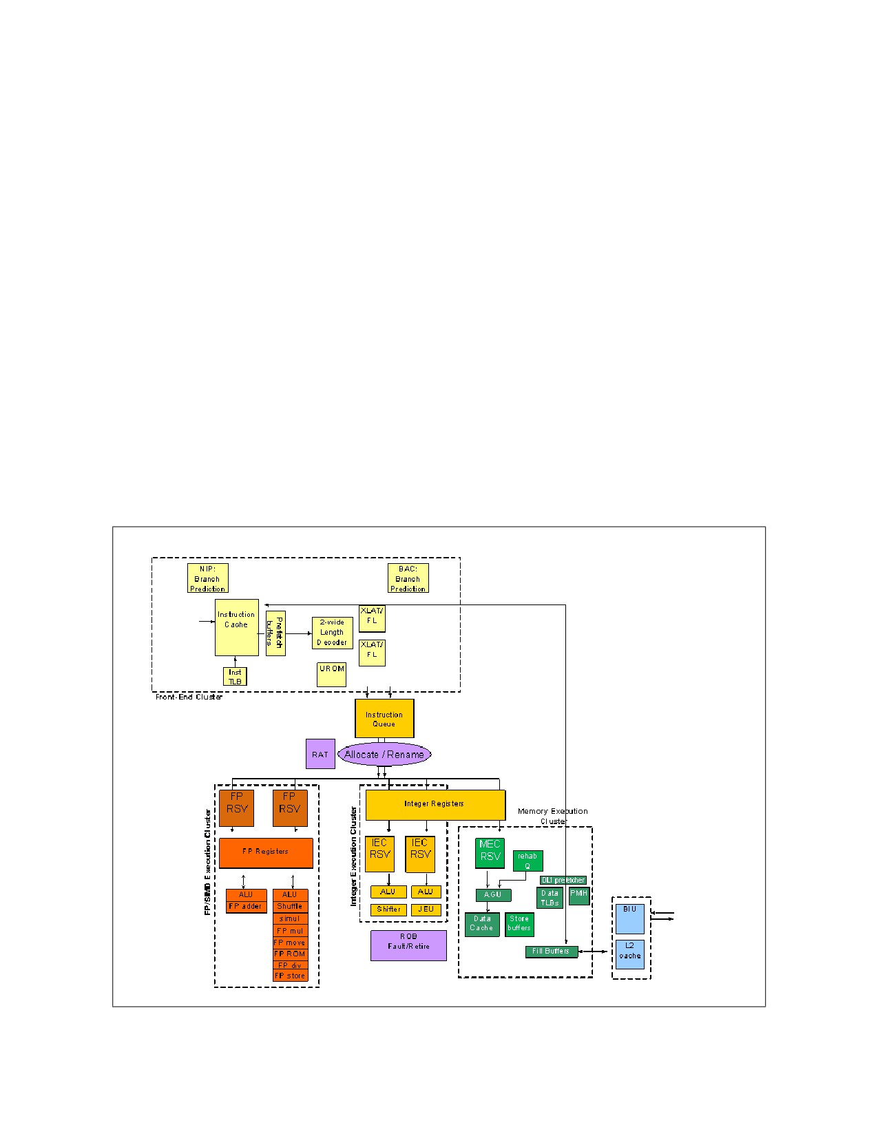
EARLIER GENERATIONS OF INTEL ATOM® MICROARCHITECTURE AND SOFTWARE OPTIMIZATION
• Out-of-order execution for integer instructions and de-coupled ordering between non-integer and
memory instructions. In contrast, the 45nm and 32nm Intel Atom microarchitecture was strictly in-
order with limited ability to exploit available instruction-level parallelism.
• Non-blocking memory instructions allowing multiple (8) outstanding misses. In previous generation
processors, problems in a single memory instruction (for example, a cache miss) caused all
subsequent instructions to stall until the problem was resolved. The new microarchitecture allows up
to 8 unique outstanding references.
• Modular system design with two cores sharing an L2 cache connected to a new integrated memory
controller using a point-to-point interface instead of the Front Side Bus.
• Instruction set enhancements to include SSE 4.1, SSE 4.2, AESNI and PCLMULQDQ.
The block diagram for the Silvermont microarchitecture is depicted in Figure 6-1. While the memory and
execute clusters were significantly redesigned for improved single thread performance, the primary
focus is still a highly efficient design in a small form factor power envelope. Each pipeline is accompanied
with a dedicated scheduling queue called a reservation station. While floating-point and memory
instructions schedule from their respective queues in program order, integer execution instructions
schedule from their respective queues out of order.
Integer instructions can be scheduled from their queues out of order in contrast to in-order execution in
previous generations. Out of order scheduling allows these instructions to tolerate stalls caused by
unavailable (re)sources. Memory instructions must generate their addresses (AGEN) in-order and
schedule from the scheduling queue in-order but they may complete out-of-order.
Non-integer instructions (including SIMD integer, SIMD floating-point, and x87 floating-point) also
schedule from their respective scheduling queue in program order. However, these separate scheduling
queues allow their execution to be decoupled from instructions in other scheduling queues.
Figure 6-2. Silvermont Microarchitecture Pipeline
Ref#: 248966-048
6-20

EARLIER GENERATIONS OF INTEL ATOM® MICROARCHITECTURE AND SOFTWARE OPTIMIZATION
The design of the microarchitecture takes into account maximizing platform performance of multiple
form factors (e.g. phones, tablets, to micro-servers) and minimizing the power and area cost due to out
of order scheduling (i.e. maximizing performance/power/cost efficiency). Intel Hyper-Threading
Technology is not supported in favor of a multi-core architecture with a shared L2 cache. The rest of this
section will cover some of the cluster-level features in more detail.
The front end cluster (FEC), shown in yellow in Figure 6-1, features a power optimized 2-wide decode
pipeline. FEC is responsible for fetching and decoding instructions from instruction memory. FEC utilizes
predecode hints from the icache to avoid costly on-the-fly instruction length determination. The front end
contains a Branch Target Buffer (BTB), plus advanced branch predictor hardware.
The front end is connected to the execution units through the Allocation, Renaming and Retirement
(ARR) cluster (lavender color in Figure 6-1). ARR receives uops from the FEC and is responsible for
resource checks. The Register Alias Table (RAT) renames the logical registers to the physical registers.
The Reorder Buffer (ROB) puts the operations back into program order and completes (retires) them. It
also stops execution at interrupts, exceptions and assists and runs program control over microcode.
Scheduling in the Silvermont microarchitecture is distributed, so after renaming, uops are sent to various
clusters (IEC: integer execution cluster; MEC: memory execution cluster; FPC: floating-point cluster) for
scheduling (shown as RSV for FP, IEC, and MEC in Figure 6-1).
There are 2 sets of reservation stations for FPC and IEC (one for each port) and a single set of reservation
stations for MEC. Each reservation station is responsible for receiving up to 2 ops from the ARR cluster in
a cycle and selecting one ready op for dispatching to execution as soon as the op becomes ready.
To support the distributed reservation station concept, load-op and load-op-store macro-instructions
requiring integer execution must be split into a memory sub-op that is sent to the MEC and resides in the
memory reservation station and an integer execution sub-op that is sent to the integer reservation
station. The IEC schedulers pick the oldest ready instruction from each of its RSVs while the MEC and the
FPC schedulers only look at the oldest instruction in their respective RSVs. Even though the MEC and FPC
clusters employ in-order schedulers, a younger instruction from a particular FPC RSV can execute before
an older instruction in the other FPC RSV for example (or the IEC or MEC RSVs).
Each execution port has specific functional units available. Table 6-3 shows the mapping of functional
units to ports for IEC (the orange units in Figure 6-1), MEC (the green units in Figure 6-1), and the FPC
(the red units in Figure 6-1). Compared to the previous Intel Atom microarchitecture, the Silvermont
microarchitecture adds an integer multiply unit (IMUL) in IEC.
Table 6-3. Function Unit Mapping of the Silvermont Microarchitecture
Cluster
Port 0
Port 1
IEC
ALU0, Shift/Rotate Unit, LEA with no index
ALU1, Bit processing unit, Jump unit, IMUL, POPCNT,
CRC32, LEA1
FPC
SIMD ALU, SIMD shift/Shuffle unit, SIMD FP
SIMD ALU, SIMD FPadd unit, F2I convert unit
mul/div/cvt unit, STTNI/AESNI/PCLMULQDQ
unit, RCP/RSQRT unit, F2I convert unit
MEC
Load/Store
NOTES:
1. LEAs with valid index and displacement are split into multiple UOPs and use both ports. LEAs with valid index execute on
port 1.
Ref#: 248966-048
6-21
EARLIER GENERATIONS OF INTEL ATOM® MICROARCHITECTURE AND SOFTWARE OPTIMIZATION
The Memory Execution Cluster (MEC) (shown in green in Figure 6-1) can support both 32-bit and 36-bit
physical addressing modes. The Silvermont microarchitecture has a 2 level Data TLB hierarchy with
support for both large (2MB or 4MB) and small page structures. A small micro TLB (referred to as uTLB)
is backed up by a larger 2nd level TLB (referred to as DTLB). A hardware page walker services misses
from both the Instruction and Data TLBs.
The MEC also owns the MEC RSV, which is responsible for scheduling of all loads and stores. Load and
store instructions go through addresses generation phase in program order to avoid on-the-fly memory
ordering later in the pipeline. Therefore, an unknown address will stall younger memory instructions.
Memory operations that incur problems (e.g. uTLB misses, unavailable resources, etc.) are put in a
separate queue called the RehabQ. This allows younger instructions (that do not incur problems) to
continue execution rather than stalling all younger instructions. The problematic instruction is later
reissued from the RehabQ when the problem is resolved. Note that load misses are not considered
problematic as the Silvermont microarchitecture features a non-blocking data cache that can sustain 8
outstanding misses.
The Bus Cluster (BIU) includes the second-level cache (L2) and is responsible for all communication with
components outside the processor core. The L2 cache supports up to 1MB with an optimized latency less
than the previous Intel Atom microarchitecture. The Front-Side Bus from earlier Intel Atom processors
has been replaced by an intra-die interconnect (IDI) fabric connecting to a newly optimized memory
controller. The BIU also houses the L2 data prefetcher.
The new core level multi-processing (or CMP) system configuration features two processor cores making
requests to a single BIU, which will handle the multiplexing between cores. This basic CMP module can be
replicated to create a quad-core configuration, or one core chopped off to create a single-core
configuration.
6.5.1
Integer Pipeline
Load pipeline stages are no longer inlined with the rest of the integer pipeline. As a result, non-load ops
can reach execute faster, and the branch misprediction penalty is effectively 3 cycles less compared to
earlier Intel Atom processors. Front end pipe stages are the same as earlier Intel Atom processors
(3 cycles for fetch, 3 cycles for decode). ARR pipestages perform out-of-order allocation and register
renaming, split the uop into parts if necessary, and send them to the distributed reservation stations.
RSV stage is where the distributed reservation station performs its scheduling. The execution pipelines
are very similar to earlier Intel Atom processors. When all parts of a uop are marked as finished, the ROB
handles final completion in-order.
6.5.2
Floating-Point Pipeline
Compared to the INT pipeline, the FP pipeline is longer. The execution stages can vary between one and
five depending on the instruction. Like other Intel microarchitectures, the Silvermont microarchitecture
needs to limit the number of FP assists (when certain floating-point operations cannot be handled
natively by the execution pipeline, and must be performed by microcode) to the bare minimum to
achieve high performance. To do this the processor should be run with exceptions masked and the DAZ
(denormal as zero) and FTZ (flush to zero) flags set whenever possible.
As mentioned, while each FPC RSV schedules instructions in-order, the RSVs can get out of order with
respect to each other.
Ref#: 248966-048
6-22
EARLIER GENERATIONS OF INTEL ATOM® MICROARCHITECTURE AND SOFTWARE OPTIMIZATION
6.6
GOLDMONT MICROARCHITECTURE
The Goldmont microarchitecture builds on the success of the Silvermont microarchitecture (see Section
6.5), and provides the following enhancements:
•
An out-of-order execution engine with a 3-wide superscalar pipeline. Specifically:
— The decoder can decode 3 instructions per cycle.
— The microcode sequencer can send 3 uops per cycle for allocation into the reservation stations.
— Retirement supports a peak rate of 3 per cycle.
•
Enhancement in branch prediction which de-couples the fetch pipeline from the instruction decoder.
•
Larger out-of-order execution window and buffers that enable deeper out-of-order execution across
integer, FP/SIMD, and memory instruction types.
•
Fully out-of-order memory execution and disambiguation. The Goldmont microarchitecture can
execute one load and one store per cycle (compared to one load or one store per cycle in the
Silvermont microarchitecture). The memory execution pipeline also includes a second level TLB
enhancement with 512 entries for 4KB pages.
•
Integer execution cluster in the Goldmont microarchitecture provides three pipelines and can execute
up to three simple integer ALU operations per cycle.
•
SIMD integer and floating-point instructions execute in a 128-bit wide engine. Throughput and
latency of many instructions have improved, including PSHUFB with 1-cycle throughput (versus 5
cycles for Silvermont microarchitecture) and many other SIMD instructions with doubled throughput;
see Table 6-19 for details.
•
Throughput and latency of instructions for accelerating encryption/description (AES) and carry-less
multiplication (PCLMULQDQ) have been improved significantly in the Goldmont microarchitecture.
•
The Goldmont microarchitecture provides new instructions with hardware accelerated secure hashing
algorithm, SHA1 and SHA256.
•
The Goldmont microarchitecture also adds support for the RDSEED instruction for random number
generation meeting the NIST SP800-90C standard.
•
PAUSE instruction latency is optimized to enable better power efficiency.
Ref#: 248966-048
6-23
EARLIER GENERATIONS OF INTEL ATOM® MICROARCHITECTURE AND SOFTWARE OPTIMIZATION
1st Level Branch
2nd Level Branch
ITLB
Predict
Predict
Instruction Cache
Decode
MSROM
Instruction Queue
Allocate Rename
Ld/St
ALU
ALU
ALU
FP/SIMD Sched
Sched
Sched
Sched
Sched
Phy Register File
Phy Register File
Addr
FP ALU
FP ALU
ALU
ALU
ALU
Gen
Ld/St
Buffers
L1 Data
TLB
Cache
L2 Cache
XQ Queue
IDI
Figure 6-3. CPU Core Pipeline Functionality of the Goldmont Microarchitecture
The front end cluster (FEC) of the Goldmont microarchitecture provides a number of enhancements over
the FEC of the Silvermont microarchitecture. The enhancements are summarized in Table 6-4.
Ref#: 248966-048
6-24

EARLIER GENERATIONS OF INTEL ATOM® MICROARCHITECTURE AND SOFTWARE OPTIMIZATION
Table 6-4. Comparison of Front End Cluster Features
Feature
Goldmont Microarchitecture
Silvermont Microarchitecture
Number of Decoders
3
2
Max Throughput of Decoders
20 Bytes per cycle
16 Bytes per cycle
Fetch and Icache Pipeline
Decoupled
Coupled
ITLB
48 entries, large page support
48 entries
Branch Mispredict Penalty
12 cycles
10 cycles
L2 Predecode Cache
16K
NA
The FEC is connected to the execution units through the Allocation, Renaming and Retirement (ARR)
cluster. Scheduling of uops is handled with distributed reservation stations across different clusters
(IEC, FPC, MEC). Each cluster has its own reservations for receiving multiple uops from the ARR. Table
6-5 compares the out-of-order scheduling characteristics between the Goldmont microarchitecture and
Silvermont microarchitecture.
Table 6-5. Comparison of Distributed Reservation Stations on Scheduling Uops
Cluster
Goldmont Microarchitecture
Silvermont Microarchitecture
IEC Reservation
3x distributed for each port
2x distributed for each port
Out-of-order within each IEC RSV and
Out-of-order within each IEC RSV and between IEC,
between IEC, across FPC, MEC
across FPC, MEC
FPC Reservation
1x unified to ports 0, 1
2x distributed for each port
Out-of-order within FPC RSV and across
In order within each FPC RSV; out-of-order between
IEC, MEC
FPC, across IEC, MEC
MEC Reservation
1x unified to ports 0, 1
1x to port 0
Out-of-order within MEC RSV and across
In order within each MEC RSV; out-of-order across
IEC, FPC
IEC, FPC
An instruction that references memory and requires integer/FP resources will have the memory uop sent
to the MEC cluster and the integer/FP uop sent to the IEC/FPC cluster. Then out-of-order execution can
commence according to the heuristic described in Table 6-5 and when resources are available. Table 6-6
shows the mapping of execution units across each port for respective clusters.
Table 6-6. Function Unit Mapping of the Goldmont Microarchitecture
Cluster
Port 0
Port 1
Port 2
ALU0, Shift/Rotate, LEA with no
ALU1, Bit processing, JEU, IMUL,
ALU2, LEA1, I2F,
IEC
index, F2I, converts/cmp, store_data
IDIV,POPCNT, CRC32, LEA, I2F, store_data
flag_merge
SIMD ALU, SIMD shift/Shuffle, SIMD
SIMD ALU, SIMD shuffle,
FPC
mul, STTNI/AESNI/PCLMULQDQ/SHA ;
FP_add, F2I compare
FP_mul, Converts, F2I convert
MEC
Load_addr
Store_addr
NOTES:
1. LEAs without index can execute on port 0, 1, or 2. LEA with valid index and displacement are split into multiple UOPs and
use both port 1 and 2. LEAs with valid index execute on port 1.
Ref#: 248966-048
6-25

EARLIER GENERATIONS OF INTEL ATOM® MICROARCHITECTURE AND SOFTWARE OPTIMIZATION
The MEC owns the MEC RSV and is responsible for scheduling all load and stores via ports 0 and 1. Load
and store instructions can go through the address generation phase in order or out-of-order. When
out-of-order address generation scheduling is available, memory execution pipeline is de-coupled from
the address generation pipeline using the load buffers and store buffers.
With out-of-order execution, situations where loads can pass an unknown store may cause memory
order issues if the load eventually depended on the unknown store and would require a pipeline flush
when the store ad-dress is known. The Goldmont microarchitecture keeps track of and minimizes such
potentially problematic load executions.
Memory operations that experienced problems (for example, uTLB misses and unavailable resources) go
back to load or store buffer for re-execution. This allows younger instructions (that do not incur
problems) to continue execution rather than stalling all younger instructions. The problematic instruction
is later re-issued (in some cases, re-issued at retirement) from the load/store buffer when the problem
is resolved. Note that load misses are considered problematic as the data cache is non-blocking and can
sustain multiple outstanding misses using write-combining buffers (WCB).
Table 6-7. Comparison of MEC Resources
MEC Resource
Goldmont Microarchitecture
Silvermont Microarchitecture
L1 Data Cache
24KB
24 KB
uTLB
32 entries
32 entries
DTLB (4KB page)
512 entries
128 entries
DTLB (2M/4M page)
32 entries
16 entries
Load-use Latency
3 cycles
3 cycles
Pipeline
1x load + 1x store
1x share by load/store
AGEN
Out-of-order
In order
WCBs
8
8
Addressing
39-bit physical, 48-bit linear
36-bit physical, 48-bit linear
6.7
GOLDMONT PLUS MICROARCHITECTURE
The Goldmont Plus microarchitecture builds on the success of the Goldmont microarchitecture (see
Section 6.6), and provides the following enhancements:
• Widen previous generation Intel Atom processor back-end pipeline to 4-wide allocation to 4-wide
retire, while maintaining 3-wide fetch and decode pipeline.
• Enhanced branch prediction unit.
•
64KB shared second level pre-decode cache (16KB in Goldmont microarchitecture).
• Larger reservation station and ROB entries to support large out-of-order window.
• Wider integer execution unit. New dedicated JEU port with support for faster branch redirection.
• Radix-1024 floating point divider for fast scalar/packed single, double and extended precision
floating point divides.
• Improved AES-NI instruction latency and throughput.
• Larger load and store buffers. Improved store-to-load forwarding latency store data from register.
• Shared instruction and data second level TLB. Paging Cache Enhancements (PxE/ePxE caches).
• Modular system design with four cores sharing up to 4MB L2 cache.
Ref#: 248966-048
6-26
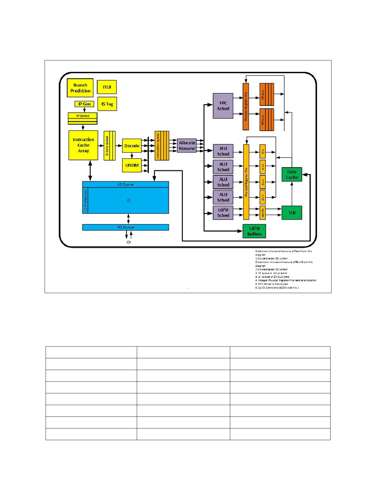
EARLIER GENERATIONS OF INTEL ATOM® MICROARCHITECTURE AND SOFTWARE OPTIMIZATION
• Support for Read Processor ID (RDP) new instruction.
Figure 6-4. CPU Core Pipeline Functionality of the Goldmont Plus Microarchitecture
The front end cluster (FEC) of the Goldmont Plus microarchitecture provides a number of enhancements
over the FEC of the Goldmont microarchitecture. The enhancements are summarized in Table 6-8.
Table 6-8. Comparison of Front End Cluster Features
Feature
Goldmont Plus Microarchitecture
Goldmont Microarchitecture
Number of Decoders
3
3
Max. Throughput Decoders
20 Bytes per cycle
20 Bytes per cycle
Fetch and Icache Pipeline
Decoupled
Decoupled
ITLB
48 entries, large page support
48 entries, large page support
2nd Level ITLB
Shared with DTLB
Branch Mispredict Penalty
13 cycles (12 cycles for certain Jcc)
12 cycles
L2 Predecode Cache
64K
16K
Ref#: 248966-048
6-27

EARLIER GENERATIONS OF INTEL ATOM® MICROARCHITECTURE AND SOFTWARE OPTIMIZATION
The FEC is connected to the execution units through the Allocation, Renaming and Retirement (ARR)
cluster. Scheduling of uops is handled with distributed reservation stations across different clusters
(IEC, FPC, MEC). Each cluster has its own reservations for receiving multiple uops from the ARR.
Table 6-9 compares the out-of-order scheduling characteristics between the Goldmont Plus
microarchitecture and Goldmont microarchitecture.
Table 6-9. Comparison of Distributed Reservation Stations on Scheduling Uops
Cluster
Goldmont Plus Microarchitecture
Goldmont Microarchitecture
IEC Reservation
4x distributed for each port
3x distributed for each port
Out-of-order within each IEC RSV and
Out-of-order within each IEC RSV and between IEC,
between IEC, across FPC, MEC
across FPC, MEC
FPC Reservation
1x unified to ports 0, 1
1x unified to ports 0, 1
Out-of-order within FPC RSV and across
Out-of-order within FPC RSV and across IEC, MEC
IEC, MEC
MEC Reservation
1x unified to ports 0, 1
1x unified to ports 0, 1
Out-of-order within MEC RSV and across
Out-of-order within MEC RSV and across IEC, FPC
IEC, FPC
An instruction that references memory and requires integer/FP resources will have the memory uop sent
to the MEC cluster and the integer/FP uop sent to the IEC/FPC cluster. Then out-of-order execution can
commence according to the heuristic described in Table 6-9 when resources are available. Table 6-10
shows the mapping of execution units across each port for respective clusters.
Table 6-10. Function Unit Mapping of the Goldmont Plus Microarchitecture
Cluster
Port 0
Port 1
Port 2
Port 3
ALU0, Shift/Rotate, LEA
ALU1, Bit processing, IMUL,
ALU2, LEA1, I2F,
IEC
with no index, F2I,
IDIV,POPCNT, CRC32, LEA,
JEU
flag_merge
converts/cmp, store_data
I2F, store_data
SIMD ALU, SIMD
shift/Shuffle, SIMD mul,
STTNI/AESNI/PCLMULQDQ/
SIMD ALU, SIMD shuffle,
FPC
SHA ;
FP_add, F2I compare
FP_mul, Converts, F2I
convert
MEC
Load_addr
Store_addr
NOTES:
1. LEAs without index can execute on port 0, 1, or 2. LEA with a valid index and displacement are split into multiple UOPs
and use both port 1 and 2. LEAs with a valid index execute on port 1.
The MEC owns the MEC RSV and is responsible for scheduling all load and stores via ports 0 and 1. Load
and store instructions can go through the address generation phase in order or out-of-order. When
out-of-order address generation scheduling is available, memory execution pipeline is de-coupled from
the address generation pipeline using the load buffers and store buffers.
With out-of-order execution, situations where loads can pass an unknown store may cause memory
order issues if the load eventually depended on the unknown store and would require a pipeline flush
when the store address is known. The Goldmont Plus microarchitecture keeps track of and minimizes
such potentially problematic load executions.
Ref#: 248966-048
6-28

EARLIER GENERATIONS OF INTEL ATOM® MICROARCHITECTURE AND SOFTWARE OPTIMIZATION
Memory operations that experienced problems (for example, uTLB misses and unavailable resources) go
back to the load or store buffer for re-execution. This allows younger instructions (that do not incur
problems) to continue execution rather than stalling all younger instructions. The problematic instruction
is later re-issued from the load/store buffer when the problem is resolved. Note that load misses are
considered problematic as the data cache is non-blocking and can sustain multiple outstanding misses
using write-combining buffers (WCB).
Goldmont Plus microarchitecture includes secondary level TLB changes to support both data and instruc-
tion side translations (Goldmont microarchitecture secondary level TLB only supports data).
6.8
CODING RECOMMENDATIONS
Most of the general coding recommendations described in Volume 1, Chapter 3, “General Optimization
Guidelines” also apply to the Intel Atom microarchitectures. The rest of this chapter describes techniques
that
supplement the general recommendations and are specific to the Intel Atom microarchitectures.
6.8.1
Optimizing The Front End
6.8.1.1
Instruction Decoder
Some IA instructions that perform complex tasks require a lookup in the microcode sequencer ROM
(MSROM) to decode them into a multiple uop flow. To determine which instructions require an MSROM
lookup, see the instruction latency/bandwidth table in Section 6.9.
Fewer instructions require MSROM lookup in the Goldmont Plus and Goldmont microarchitecture than in
the Silvermont microarchitecture, though the Silvermont microarchitecture also improved significantly
over prior generations in this area; Section 6.9 provides more details. It is advisable to avoid ucode flows
where possible. Table 6-11 provides alternate non-MSROM instruction sequences that can replace an
instruction that decodes from MSROM.
Table 6-11. Alternatives to MSROM Instructions
Recommendation for Goldmont Plus and
Instruction from MSROM
Recommendation for Silvermont
Goldmont
CALL m16/m32/m64
Load + CALL reg
Load + CALL reg
PUSH m16/m32/m64
Load + PUSH reg
Use as is (non MSROM)
LEAVE
No recommended replacement
Use as is (non MSROM)
FLD/FST/FSTP m80fp
No recommended replacement
Use as is (non MSROM)
FCOM+FNSTSW
FCOMI
FCOMI
Use (I)MUL r16, r/m16 if extended precision
Use (I)MUL r16, r/m16 if extended precision
(I)MUL r/m16 (Result DX:AX)
not required, or (I)MUL r32, r/m32
not required, or (I)MUL r32, r/m32
Use (I)MUL r32, r/m32 if extended precision
(I)MUL r/m32 (Result EDX:EAX)
Use as is (non MSROM)
not required, or (I)MUL r64, r/m64
Use (I)MUL r64, r/m64 if extended precision
(I)MUL r/m64 (Result RDX:RAX)
Use as is (non MSROM)
not required
PEXTRB/D/Q
No recommended replacement
Use as is (non MSROM)
PMULLD
No recommended replacement
Use as is (non MSROM)
Ref#: 248966-048
6-29
EARLIER GENERATIONS OF INTEL ATOM® MICROARCHITECTURE AND SOFTWARE OPTIMIZATION
Tuning Suggestion 1. Use the perfmon counter MS_DECODED.MS_ENTRY to find the number of
instructions that need the MSROM (the count will include any assist or fault that occurred).
Assembly/Compiler Coding Rule 1. (M impact, M generality) Try to keep the I-footprint small to
get the best reuse of the predecode bits.
Avoid I-cache aliasing/thrashing since the incorrect predecode bits result in reduction of decode
throughput in one instruction every 3 cycles.
Tuning Suggestion 2. Use the perfmon counter DECODE_RESTRICTION.PREDECODE_WRONG to
count the number of times that a decode restriction reduced instruction decode throughput because
predecoded bits are incorrect.
6.8.1.2
Front End High IPC Considerations
In general front end restrictions are not typically a performance limiter until you reach higher (>1)
Instructions Per Cycle (IPC) levels.
The decode restrictions that must be followed to get full decode bandwidth per cycle through the
decoders include:
• MSROM instructions should be avoided if possible. A good example is the memory form of CALL near
indirect. It will often be better to perform a load into a register and then perform the register version
of CALL.
• The total length of the instruction bytes that can be decoded each cycle varies by microarchitecture.
— Silvermont microarchitecture: up to 16 bytes per cycle with instruction not more than 8 bytes in
length. For an instruction length exceeding 8 bytes, only one instruction per cycle is decoded on
decoder 0.
— Goldmont and later microarchitecture: up to 20 bytes per cycle depending on alignment
(for example, if the first instruction of three consecutive instructions is aligned on 4-Byte
boundary and the 3 instruction sequence meets decode restrictions. For an instruction length
exceeding 8 bytes, it is not restricted to decoder 0 or one per cycle.
• An instruction with multiple prefixes can restrict decode throughput. The restriction is on the length
of bytes combining prefixes and escape bytes. There is a 3 cycle penalty when the escape/prefix
count exceeds the following limits as specified per microarchitectures.
— Silvermont microarchitecture: the limit is 3 bytes.
— Goldmont and later microarchitecture: the limit is 4 bytes. Thus, SSE4 or AES instruction that
accesses one of the upper 8 registers do not incur a penalty.
— Only decoder 0 can decode an instruction exceeding the limit of prefix/escape byte restriction on
the Silvermont and Goldmont microarchitectures.
• The maximum number of branches that can be decoded each cycle is 1 for the Silvermont
microarchitecture and 2 for the Goldmont microarchitecture. Prevent a re-steer penalty by avoiding
back-to-back conditional branches.
Unlike the previous generation, the Silvermont and later microarchitectures can decode two x87
instructions in the same cycle without incurring a 2-cycle penalty. Branch decoder restrictions are also
relaxed. In earlier Intel Atom processors, decoding past a conditional or indirect branch in decoder 0
resulted in a 2-cycle penalty.
The Silvermont microarchitecture can decode past conditional and indirect branch instructions in decoder
0. However, if the next instruction (on decoder 1) is also a branch, there is a 3-cycle penalty for the
second branch instruction.
The Goldmont and later microarchitecture can decode one predicted not-taken branches in decoder 0 or
decoder 1, plus another branch in decoder 2 without the 3-cycle re-steer penalty. However, if there are
two predicted not-taken branches at decoder 0 and 1, the second branch at decoder 1 will incur a 3-cycle
penalty.
For a branch target that is a predicted taken conditional branch or unconditional branch, it is decoded
with a one cycle bubble across all generations of Intel Atom processors.
Ref#: 248966-048
6-30

EARLIER GENERATIONS OF INTEL ATOM® MICROARCHITECTURE AND SOFTWARE OPTIMIZATION
Assembly/Compiler Coding Rule 2. (MH impact, H generality) Minimize the use of instructions
that have the following characteristics to achieve more than one instruction per cycle throughput:
(i) using the MSROM, (ii) exceeding the limit of escape/prefix bytes, (iii) more than 8 bytes long, or
(iv) have back to back branches.
For example, an instruction with 3 bytes of prefix/escape and accessing the lower 8 registers can decode
normally in the Silvermont, Goldmont and later microarchitectures. For instance:
PCLMULQDQ 66 0F 3A 44 C7 01 pclmulqdq xmm0, xmm7, 0x1
To access any of the upper 8 XMM registers, XMM8-15, an additional byte with REX prefix is necessary.
Consequently, it will decode normally in the Goldmont and later microarchitecture, but incur a decode
penalty in the Silvermont microarchitecture. For instance:
PCLMULQDQ 66 41 0F 3A 44 C0 01 pclmulqdq xmm0, xmm8, 0x1
(Note the REX byte 41, in between the 66 and the 0F 3A.)
The 3-cycle penalty applies whenever the combined prefix/escape bytes exceed the decode restriction
limit. Also, it forces the instruction to be decoded on decoder 0. Additionally, when decoding an
instruction exceeding the prefix/escape length limit, not on decoder 0, there is an extra delay to re-steer
to decoder 0 (for a total of a 6 cycle penalty for the decoder). Therefore, when hand writing high
performance assembly, be aware of these cases. It would be beneficial to pre-align these cases to
decoder 0 if they occur infrequently using a taken branch target or MS entry point as a decoder 0
alignment vehicle. NOP insertion should be used only as a last resort as NOP instructions consume
resources in other parts of the pipeline. Similar alignment is necessary for MS entry points which suffer
the additional 3 cycle penalty if they align originally to decoder 1. The penalty associated with a
prefix/escape length limit and re-steer apply to both Silvermont, Goldmont and later microarchitectures.
Table 6-12 compares decoder capabilities between microarchitectures.
Table 6-12. Comparison of Decoder Capabilities
Goldmont Plus and Goldmont
Silvermont Microarchitecture
Microarchitecture
Width
3
2
20 bytes per cycle (1st instr. aligned to 4B
Max Throughput
16 bytes per cycle (1st instr. <= 8 bytes))
boundary and decoder 1 and 2 restrictions )
Prefix/Escape Limit
4 bytes
3 bytes
Branch
2
1
6.8.1.3
Branching Across 4GB Boundary
Another important performance consideration from a front end standpoint is branch prediction. For
64-bit applications, branch prediction performance can be negatively impacted when the target of a
branch is more than 4GB away from the branch. This is more likely to happen when the application is split
into shared libraries. Newer glibc versions can put the shared libraries into the first 2GB to avoid this
problem (since 2.23). The environment variable LD_PREFER_MAP_32BIT_EXEC=1 has to be set.
Developers can build statically to improve the locality in their code. Building with LTO should further
improve performance.
6.8.1.4
Loop Unrolling and Loop Stream Detector
The Silvermont and later microarchitectures include a Loop Stream Detector (LSD) that provides the
back end with uops that are already decoded. This provides performance and power benefits. When the
LSD is engaged, front end decode restrictions, such as number of prefix/escape bytes and instruction
length, no longer apply.
One way to reduce the overhead of loop maintenance code and increase the amount of independent work
in a loop is software loop unrolling. Unfortunately care must be taken on where it is utilized because loop
Ref#: 248966-048
6-31
EARLIER GENERATIONS OF INTEL ATOM® MICROARCHITECTURE AND SOFTWARE OPTIMIZATION
unrolling has both positive and negative performance effects. The negative performance effects are
caused by the increased code size and increased BTB and register pressure. Furthermore, loop unrolling
can increase the loop size beyond the limits of the LSD. The LSD loop size limit varies with
microarchitecture; it is 27 for the Goldmont and later microarchitecture with a three-wide decoder, and
28 for the Silvermont microarchitecture. Care must be taken to keep the loop size under the LSD limit.
User/Source Coding Rule 1. (M impact, M generality) Keep per-iteration instruction count below
28 when considering loop unrolling technique on short loops with high iteration count.
Tuning Suggestion 3. Use the BACLEARS.ANY perfmon counter to see if the loop unrolling is causing
too much pressure. Use the ICACHE.MISSES perfmon counter to see if loop unrolling is having an
excessive negative effect on the instruction footprint.
6.8.1.5
Mixing Code and Data
Intel Atom processors perform best when code and data are on different pages. Software should avoid
sharing code and data in the same page to avoid false SMC conditions. This recommendation applies to
all page sizes.
6.8.2
Optimizing The Execution Core
6.8.2.1
Scheduling
The Silvermont microarchitecture is less sensitive to instruction ordering than its predecessors due to the
introduction of out-of-order execution for integer instructions. FP instructions have their own reservation
stations but still execute in order with respect to each other. Memory instructions also issue in order but
with the addition of the Rehab Queue, they can complete out of order and memory system delays are no
longer blocking.
The Goldmont and later microarchitecture features fully out-of-order execution across the IEC, FPC, and
MEC pipelines, and is supported by enhancements ranging from 3 ports for IEC, 128-bit data path of FPC
units, dedicated load address and store address pipelines.
Tuning Suggestion 4. Use the perfmon counter UOPS_NOT_DELIVERED.ANY (NO_ALLOC_CYCLE.ANY
on Silvermont microarchitecture) as an indicator of performance bottlenecks in the back end. This
includes delays in the memory system and execution delays.
6.8.2.2
Address Generation
The Silvermont microarchitecture eliminated address generation limitations in previous generations. As
such, using LEA or ADD instructions to generate addresses are equally effective on the Silvermont and
later microarchitectures.
The rule of thumb for ADDs and LEAs is that it is justified to use LEA with a valid index and/or
displacement for non-destructive destination purposes (especially useful for stack offset cases), or to use
a SCALE. Otherwise, ADD(s) are preferable.
6.8.2.3
FP Multiply-Accumulate-Store Execution
With Goldmont and later microarchitectures, a unified FPC reservation station eliminates the
performance issue that can happen in the Silvermont microarchitecture due to intra-port dependence of
in-order scheduling of FPC uops. The paragraphs below and Example 6-7 illustrate the problem.
FP arithmetic instructions executing on different ports can execute out-of-order with respect to each
other in the Silvermont microarchitecture. As a result, in unrolled loops with multiplication results feeding
into add instructions which in turn produce results for store instructions, grouping the store instructions
at the end of the loop will improve performance. This allows it to overlap the execution of the multiplies
and the adds. Consider the example shown in Example 6-7.
Ref#: 248966-048
6-32

EARLIER GENERATIONS OF INTEL ATOM® MICROARCHITECTURE AND SOFTWARE OPTIMIZATION
Example 6-7. Unrolled Loop Executes In-Order Due to Multiply-Store Port Conflict
1
1
1
1
1
1
1
1
1
Instruction
1
2
3
4
5
6
7
8
9
0
1
2
3
4
5
6
7
8
E
E
E
E
E
mulps, xmm1, xmm1
X
X
X
X
X
1
2
3
4
5
E
E
E
addps xmm1, xmm1
X
X
X
1
2
3
E
movaps mem, xmm1
X
1
E
E
E
E
E
mulps, xmm2, xmm2
X
X
X
X
X
1
2
3
4
5
E
E
E
addps xmm2, xmm2
X
X
X
1
2
3
E
movaps mem, xmm2
X
1
Due to the data dependence, the add instructions cannot start executing until the corresponding multiply
instruction is executed. Because multiplies and stores use the same port, they have to execute in
program order. This means the second multiply instruction cannot start execution even though it is
independent from the first multiply and add instructions. If you group the store instructions together at
the end of the loop as shown below, the second multiply instruction can execute in parallel with the first
multiply instruction (note the one-cycle bubble when multiplies are overlapped).
Example 6-8. Grouping Store Instructions Eliminates Bubbles and Improves IPC
Instruction
1
2
3
4
5
6
7
8
9
10
11
mulps, xmm1, xmm1
EX1
EX2
EX3
EX4
EX5
addps xmm1, xmm1
EX1
EX2
EX3
mulps, xmm2, xmm2
bubble EX1
EX2
EX3
EX4
EX5
addps xmm2, xmm2
EX1
EX2
EX3
movaps mem, xmm1
EX1
movaps mem, xmm2
EX1
6.8.2.4
Integer Multiply Execution
The Silvermont and later microarchitectures have a dedicated integer multiplier to accelerate
commonly-used forms of integer multiply flows. Table 6-13 shows the latency and instruction forms of
mul/imul instructions that are accelerated and not using MSROM.
Ref#: 248966-048
6-33

EARLIER GENERATIONS OF INTEL ATOM® MICROARCHITECTURE AND SOFTWARE OPTIMIZATION
Table 6-13. Integer Multiply Operation Latency
Goldmont Plus and
Integer Multiply Operations
Output
Silvermont Latency
Goldmont Latency
imul/mul r/m8
16
4u
5u
imul/mul r/m16
32
4u
5u
imul/mul r/32
64
3
4u
imul/mul r/m64
128
5
7u
imul/mul r16, r/m16; r16, r/m16, imm
16
4u
4u
imul/mul r32, r/m32; r32, r/m32, imm
32
3
3
imul/mul r64, r/m64; r64, r/m64, imm8
64
5
5
u: ucode flow from MSROM
The multiply forms with microcode flows should be avoided.
6.8.2.5
Zeroing Idioms
XOR / PXOR / XORPS / XORPD instructions are commonly used to force register values to zero when the
source and the destination register are the same (e.g. XOR eax, eax).
This method of zeroing is preferred by compilers instead of the equivalent MOV eax, 0x0 instructions as
the MOV encoding is larger than the XOR in code bytes.
The Silvermont and later microarchitectures have special hardware support to recognize these cases and
mark both the sources as valid in the architectural register file. This helps the XOR execute faster since
any value XORed with itself will accomplish the necessary zeroing.
The logic will also support PXOR, XORPS, and XORPD idioms.
In Silvermont microarchitecture, zero-idiom, a 64-bit general purpose operand using REX.W, will
experience delay. However, zero-idiom is supported with XMM8-XMM15 or the upper 8 general purpose
registers without REX.W. To clear r8, it is sufficient to use XOR r8d, r8d.
Goldmont and later microarchitecture supports these zero-idioms for 64-bit operands.
6.8.2.6
NOP Idioms
NOP instruction is often used for padding or alignment purposes. The Goldmont and later
microarchitecture has hardware support for NOP handling by marking the NOP as completed without
allocating it into the reservation station. This saves execution resources and bandwidth. Retirement
resource is still needed for the eliminated NOP.
6.8.2.7
Move Elimination and ESP Folding
Move elimination is supported in Goldmont and later microarchitecture. When move elimination is in
effect, these instructions can execute with higher throughput in addition to zero-cycle latency. Specifi-
cally, 32-bit and 64-bit operand size of MOV, and
MOVAPS/MOVAPD/MOVDQA/MOVDQU/MOVUPS/MOVUPD with XMM are supported and have throughput
of 0.33 cycle if move elimination is in effect. MOVSX and MOVZX do not support move elimination.
Stack operation using PUSH/POP/CALL/RET is more efficient with the Goldmont and later
microarchitecture than with the Silvermont microarchitecture. Computing the stack pointer address does
Ref#: 248966-048
6-34
EARLIER GENERATIONS OF INTEL ATOM® MICROARCHITECTURE AND SOFTWARE OPTIMIZATION
not consume allocation and execution resources in the Goldmont and later microarchitecture.
Additionally, throughput of PUSH/POP is increased from one to three per cycle.
6.8.2.8
Stack Manipulation Instruction
The memory forms of indirect CALL m16/m32/m64 are decoded into a uop flow from MSROM. Indirect
CALL with target specified in a register can avoid the delays. Thus, loading the target address to a
register, followed by an indirect CALL via register operand is recommended.
In the Goldmont and later microarchitecture, PUSH m16/m32/m64 do not require MSROM to decode.
The same is also true with the LEAVE instruction.
In the Silvermont microarchitecture, PUSH m16/m32/m64 and LEAVE require MSROM to decode.
6.8.2.9
Flags usage
Many instructions have an implicit data result that is captured in a flags register. These results can be
consumed by a variety of instructions such as conditional moves (cmovs), branches and even a variety of
logic/arithmetic operations (such as rcl). The most common instructions used in computing branch
conditions are compare instructions (CMP). Branches dependent on the CMP instruction can execute in
the next cycle. The same is true for branch instructions dependent on ADD or SUB instructions.
INC and DEC instructions require an additional uop to merge the flags as they are partial flag writers. As
a result, a branch instruction depending on an INC or a DEC instruction incurs a 1 cycle penalty.
Note that this penalty only applies to branches that are directly dependent on the INC or DEC instruction.
Assembly/Compiler Coding Rule 3. (M impact, M generality) Use CMP/ADD/SUB instructions to
compute branch conditions instead of INC/DEC instructions whenever possible.
6.8.2.10 SIMD Floating-Point and X87 Instructions
In the Silvermont microarchitecture, only a subset of the SIMD FP execution units are implemented with
a 128-bit wide data path. In Goldmont and later microarchitecture, SIMD FP units are implemented with
a 128-bit data path. In general, packed SIMD instructions complete with one cycle less in latency and
twice the throughput in the Goldmont and later microarchitecture, compared to the Silvermont
microarchitecture.
In particular, MULPD latency is accelerated from 7 to 4 cycles, with 4-fold throughput from every 4 cycles
to 1 per cycle.
Latency and throughput of X87 extended precision load and store, FLD m80fp, and FST/FSTP m80fp are
also improved in the Goldmont and later microarchitecture. See Table 6-19 for more details.
In the Goldmont Plus microarchitecture, Floating point divider is upgraded to radix-1024 based design.
Floating point divide and square root latency and bandwidth are significantly improved.
6.8.2.11 SIMD Integer Instructions
In the Silvermont microarchitecture, a relatively small subset of the SIMD integer instructions can
execute with throughput of two instructions per cycle. In the Goldmont and later microarchitecture,
many more SIMD integer instructions can complete at a rate of two instructions per cycle.
Latency and/or throughput improvements in the Goldmont and later microarchitecture include other
SIMD integer instructions that execute only one port. For example, PMULLD has an eleven-cycle latency
and throughput of one every eleven cycles in the Silvermont microarchitecture. It has five-cycle latency
and throughput of one every two cycles in the Goldmont and later microarchitectures.
In general, SIMD integer multiply hardware is significantly faster (four-cycle latency) and higher
throughput (one cycle throughput) than in the Silvermont microarchitecture. Additionally,
PADDQ/PSUBQ has two-cycle latency and throughput of every two cycles, compared to four-cycle
latency and throughput every four cycles in the Silvermont microarchitecture. PSHUFB has one-cycle
Ref#: 248966-048
6-35
EARLIER GENERATIONS OF INTEL ATOM® MICROARCHITECTURE AND SOFTWARE OPTIMIZATION
latency and throughput in the Goldmont and later microarchitectures, compared to five-cycle latency and
throughput of every five cycles. See Table 6-19 for more details.
6.8.2.12 Vectorization Considerations
In the Silvermont microarchitecture, opportunity for profitable vectorization may be limited by the
availability of high-throughput implementation SIMD execution units or SIMD instructions that require
MSROM to decode into longer flows.
The Goldmont and later microarchitectures allows compiler, as well as direct programming, to profit from
vectorization due to improvement in latency and throughput across a wide variety of SIMD instructions.
Assembly/Compiler Coding Rule 4. (M impact, M generality) Avoid MSROM instructions for code
vectorization.
6.8.2.13 Other SIMD Instructions
The Silvermont microarchitecture supports AESNI and PCLMULQDQ to accelerate performance of various
cryptographic algorithms like AES and AES-GCM for block encryption/decryption.
In the Goldmont and later microarchitectures, the execution hardware is improved from execution
latency, throughput to decode throughput. For example, PCLMULQDQ has latency of 6 cycles with
throughput of every four cycles in the Goldmont microarchitecture, compared to ten-cycle latency and
throughput of every ten cycles in the Silvermont microarchitecture.
Additionally, the Goldmont and later microarchitecture supports SHANI to accelerate the performance of
secure hashing algorithms like SHA1 and SHA256. More details about the secure hashing algorithms and
SHANI can be found at
https://software.intel.com/en-us/articles/intel-sha-extensions.
Examples and reference implementation of using the Intel SHA extensions can be found at:
https://software.intel.com/en-us/articles/intel-sha-extensions-implementations.
6.8.2.14 Instruction Selection
Table 6-14 summarizes the latency for floating-point and SIMD integer operations in the Silvermont
microarchitecture. The throughput column is expressed in number of cycles per instruction that
execution can complete with all available execution units employed (for example, 4 indicates the same
instruction can complete execution every four cycles; 0.33 indicates three identical instructions can
complete execution each cycle).
Ref#: 248966-048
6-36

EARLIER GENERATIONS OF INTEL ATOM® MICROARCHITECTURE AND SOFTWARE OPTIMIZATION
Table 6-14. Floating-Point and SIMD Integer Latency
Goldmont Plus
Goldmont
Silvermont
Through
Through
Throughp
Latency
Latency
Latency
put
put
ut
SIMD integer ALU
128-bit ALU/logical/move
1
0.5
1
0.5
1
0.5
64-bit ALU/logical/move
1
0.5
1
0.5
1
0.5
SIMD integer shift
128-bit
1
0.5
1
0.5
1
1
64-bit
1
0.5
1
0.5
1
1
SIMD shuffle
128-bit
1
0.5
1
0.5
1
1
64-bit
1
0.5
1
0.5
1
1
SIMD integer multiplier
128-bit
4
1
4
1
5
2
64-bit
4
1
4
1
4
1
FP Adder
x87 (fadd)
3
1
3
1
3
1
scalar (addsd, addss)
3
1
3
1
3
1
packed (addpd, addps)
3
1
3
1
4
2
FP Multiplier
x87 (fmul)
5
2
5
2
5
2
scalar single-precision (mulss)
4
1
4
1
4
1
scalar double-precision (mulsd)
4
1
4
1
5
2
packed single-precision (mulps)
4
1
4
1
5
2
packed double-precision (mulpd)
4
1
4
1
7
4
Converts
CVTDQ2PD, CVTDQ2PS, CVTPD2DQ,
CVTPD2PI, CVTPD2PS, CVTPI2PD,
4
1
4
1
5
2
CVTPS2DQ, CVTPS2PD, CVTTPD2DQ,
CVTPD2PI, CVTPS2DQ
CVTPI2PS, CVTPS2PI, CVTSD2SI,
CVTSD2SS, CVTSI2SD,
4
1
4
1
4
1
CVTSI2SS, CVTSS2SD, CVTSS2SI,
CVTTPS2PI, CVTTSD2SI, CVTTSS2SI
Ref#: 248966-048
6-37

EARLIER GENERATIONS OF INTEL ATOM® MICROARCHITECTURE AND SOFTWARE OPTIMIZATION
Table 6-14. Floating-Point and SIMD Integer Latency (Contd.)
Goldmont Plus
Goldmont
Silvermont
Through
Through
Throughp
Latency
Latency
Latency
put
put
ut
FP Divider
x87 fdiv (extended-precision)
15
11
39
39
39
39
x87 fdiv (double-precision)
14
10
34
34
34
34
x87 fdiv (single-precision)
11
7
19
19
19
19
scalar single-precision (divss)
11
7
19
18
19
17
scalar double-precision (divsd)
14
10
34
33
34
32
packed single-precision (divps)
16
12
36
35
39
39
packed double-precision (divpd)
22
18
66
65
69
69
Note that scalar SSE single precision multiples are one cycle faster than most FP operations. From
inspection of the table you can also see that packed SSE doubles have a slightly larger latency and
smaller throughput compared to their scalar counterparts.
Assembly/Compiler Coding Rule 5. (M impact, M generality) Favor SSE floating-point
instructions over x87 floating point instructions.
Assembly/Compiler Coding Rule 6. (MH impact, M generality) Run with exceptions masked and
the DAZ and FTZ flags set (whenever possible).
Tuning Suggestion 5. Use the perfmon counters MACHINE_CLEARS.FP_ASSIST to see if floating
exceptions are impacting program performance.
6.8.2.15 Integer Division
In Silvermont microarchitecture, integer division requires microcode flows that are relatively long and
slow. Its latency can vary profoundly on the input value and data sizes. In Goldmont and later
microarchitecture, there is hardware enhancement for short-precision forms of DIV/IDIV without using
MSROM. DIV/IDIV forms needing higher precision do use MSROM, but are also accelerated from the
hardware enhancement. Table 6-15 and Table 6-16 show the latency range for divide instructions, and
the instructions that require MSROM are noted with the superscript ‘u’.
Table 6-15. Unsigned Integer Division Operation Latency
Goldmont
Dividend
Divisor
Quotient
Remainder
Silvermontu
Plus/Goldmont
DIV r8
AX
r8
AL
AH
25
11-12
DIV r16
DX:AX
r16
AX
DX
26-30
12-17u
DIV r32
EDX:EAX
r32
EAX
EDX
26-38
12-25u
DIV r64
RDX:RAX
r64
RAX
RDX
38-123
12-41u
Ref#: 248966-048
6-38

EARLIER GENERATIONS OF INTEL ATOM® MICROARCHITECTURE AND SOFTWARE OPTIMIZATION
Table 6-16. Signed Integer Division Operation Latency
Goldmont
Dividend
Divisor
Quotient
Remainder
Silvermontu
Plus/Goldmont
IDIV r8
AX
r8
AL
AH
34
11-12
IDIV r16
DX:AX
r16
AX
DX
35-40
12-17u
IDIV r32
EDX:EAX
r32
EAX
EDX
35-47
12-25u
IDIV r64
RDX:RAX
r64
RAX
RDX
49-135
12-41u
User/Source Coding Rule 2. (M impact, L generality) Use divides only when really needed and
take care to use the correct data size and sign so that you get the most efficient execution.
Tuning Suggestion 6. Use the perfmon counter CYCLES_DIV_BUSY.ANY to see if the divides are a
bottleneck in the program.
If one needs unaligned groups of packed singles where the whole array is aligned, the use of PALIGNR is
recommend over MOVUPS. For instance, load A[x+y+3:x+y] where x and y are loop variables; it is
better to calculate x+y, round down to a multiple of 4 and use a MOVAPS and PALIGNR to get the
elements (rather than a MOVUPS at x+y). While this may look longer, the integer operations can execute
in parallel to FP ones. This will also avoid the periodic MOVUPS that splits a line at the cost of
approximately 6 cycles.
User/Source Coding Rule 3. (M impact, M generality) Use PALIGNR when stepping through
packed single elements
6.8.2.16 Integer Shift
When using an integer shift instruction with shift count in a register (i.e., CL), there is a one cycle bubble
for scheduling if the count register is produced by the preceding instruction in the execution pipeline.
Thus, the instruction producing the shift count should be hoisted whenever possible.
Additionally, double shift instructions (SHLD/SHRD) operating on 64-bit input data require long MSROM
flows. In the Silvermont microarchitecture, SHRD with a 32-bit destination register and immediate shift
count is decoded from the MSROM but the corresponding SHLD is not. In the Goldmont and later
microarchitecture, SHLD/SHRD with 32-bit destination register and immediate shift count are not
decoded from the MSROM. SHLD/SHRD with 32-bit destination memory operand or with CL shift count
are decoded from the MSROM on both Silvermont and Goldmont.
F.8.2.17 Pause Instruction
In the Goldmont and later microarchitecture, the latency of the PAUSE instruction is similar to that of the
Skylake microarchitecture to achieve better power saving with thread synchronization primitives.
6.8.3
Optimizing Memory Accesses
6.8.3.1
Reduce Unaligned Memory Access with PALIGNR
When working with single-precision FP or dword data arrays, loading 4 consecutive elements often
encounter memory accesses that are not 16-Byte aligned. For example, a nested loop iteration with an
array using two iterating indices, ‘i’, ‘j’ in A[i + j]. When loading 16 bytes from memory using “i+j” as the
effective index that increments by 1 in an inner loop, unaligned access will occur 3 of 4 accesses.
These unaligned memory access can be avoided. Assuming the base of the array is 16-Bytes aligned,
loading 16 bytes should be done with an effective index that is a multiple of 4, followed by PALIGNR with
two consecutive 16-byte chunks already loaded in XMM, with the imm8 constant derived from 4*
remainder of the original “i+j”.
Ref#: 248966-048
6-39
EARLIER GENERATIONS OF INTEL ATOM® MICROARCHITECTURE AND SOFTWARE OPTIMIZATION
Assembly/Compiler Coding Rule 7. (M impact, M generality) Use PALIGNR when stepping
through packed single-precision FP or dword elements.
6.8.3.2
Minimize Memory Execution Issues
In the Goldmont and later microarchitecture, fully out-of-order execution in the MEC allows loads to pass
older stores which have not yet resolved their address. If the load did depend on the older store, the
hardware detects this situation and the load and subsequent operations need to be re-executed. The
programmer can use a performance counter event to assess and locate the cause of such re-execution.
In the Silvermont microarchitecture, its RehabQ needs to deal with several types of execution problems
in the MEC. The issues include: load blocks, load/store splits, locks, TLB misses, unknown addresses, and
too many stores. The perfmon counter’s REHABQ in the Silvermont microarchitecture can be used to
assess problems specific to the Silvermont microarchitecture.
Tuning Suggestion 7. Use the perfmon counters MACHINE_CLEAR.DISAMBIGUATION to assess the
impact of loads passing older unknown stores on application performance with the Goldmont
microarchitecture and its descendants.
6.8.3.3
Store Forwarding
Forwarding is significantly improved in the Silvermont and later microarchitectures compared to prior
generations. A store instruction will forward its data to a receiving load instruction if the following are
true:
• The forwarding store and the receiving load start at the same address.
• The receiving load is smaller than or equal to the forwarding store in terms of width.
• The forwarding store or the receiving load do not incur cache line splits.
Table 6-17 and Table 6-18 illustrate various situations of successful forwarding versus situations where
preceding stores cannot be forwarded.
Table 6-17. Store Forwarding Conditions (1 and 2 Byte Stores)
Load Alignment
Store
Load
0
1
2
3
4
5
6
7
8
9
10
11
12
13
14
15
Size
Size
1
1
F
2
1
F
N
2
F
N
Table 6-18. Store Forwarding Conditions (4-16 Byte Stores)
Load Alignment
Store
Load
0
1
2
3
4
5
6
7
8
9
10
11
12
13
14
15
Size
Size
4
1
F
N
F
N
2
F
N
F
N
4
F
N
N
N
Ref#: 248966-048
6-40

EARLIER GENERATIONS OF INTEL ATOM® MICROARCHITECTURE AND SOFTWARE OPTIMIZATION
Table 6-18. Store Forwarding Conditions (4-16 Byte Stores)
Load Alignment
8
1
F
N
N
N
N
N
N
N
2
F
N
N
N
N
N
N
N
4
F
N
N
N
N
N
N
N
8
F
N
N
N
N
N
N
N
16
1
F
N
N
N
N
N
N
N
N
N
N
N
N
N
N
N
2
F
N
N
N
N
N
N
N
N
N
N
N
N
N
N
N
4
F
N
N
N
N
N
N
N
N
N
N
N
N
N
N
N
8
F
N
N
N
N
N
N
N
N
N
N
N
N
N
N
N
16
F
N
N
N
N
N
N
N
N
N
N
N
N
N
N
N
If one (or more) of these conditions is not satisfied, the load is blocked and put into the RehabQ to reissue
again.
To eliminate/avoid store forwarding problems, use the guidelines below (in order of preference):
• Use registers instead of memory.
• Hoist the store as early as possible (stores happen later in the pipeline than loads, so the store needs
to be hoisted many instructions earlier than the load).
The cost of a successful forwarding varies with microarchitectures. The cost is 3 cycles in the Silvermont
microarchitecture (that is, if the store executes at cycle n, the load will execute at cycle n+3). The cost is
4 cycles in the Goldmont microarchitecture. Intel Goldmont Plus microarchitecture optimizes certain
store data from register operation to reduce store to load forwarding latency to 3 cycle.
6.8.3.4
PrefetchW Instruction
The Silvermont and later microarchitectures support the PrefetchW instruction (0f 0d /1). This instruction
is a hint to the hardware to prefetch the specified line into the cache with a read-for-ownership request.
This can allow later stores to that line to complete faster than they would if the line was not prefetched
or was prefetched with a different instruction. All prefetch instructions may cause performance loss if
misused. Care should be used to ensure that prefetch instructions, including PrefetchW, actually improve
performance. The instruction opcode 0f 0d /0 continues to be a NOP. It does not prefetch the indicated
line.
6.8.3.5
Cache Line Splits and Alignment
Cache line splits cause load and store instructions to operate at reduced bandwidth. As a result, they
should be avoided where possible.
Tuning Suggestion 8. Use the REHABQ.ST_SPLIT and REHABQ.LD_SPLIT perfmon counters to locate
splits, and to count the number of split operations.
While aligned accesses are preferred, the Silvermont microarchitecture has hardware support for
unaligned references. As such, MOVUPS/MOVUPD/MOVDQU instructions are all single UOP instructions in
contrast to previous generation Intel Atom processors.
6.8.3.6
Segment Base
For simplicity, the AGU in the Silvermont microarchitecture assumes that the segment base will be zero.
However, while studies have shown that this is overwhelmingly true, there are times when a non-zero
segment base (NZB) must be used. When using NZBs, keep the segment base cache line (0x40) aligned
if at all possible. NZB address generation involves a 1 cycle penalty in the Silvermont microarchitecture.
In Goldmont and later microarchitecture, NZB address generation can maintain one per cycle.
Ref#: 248966-048
6-41

EARLIER GENERATIONS OF INTEL ATOM® MICROARCHITECTURE AND SOFTWARE OPTIMIZATION
6.8.3.7
Copy and String Copy
Compilers typically provide libraries with memcpy/memset routines that provide good performance while
managing code size and alignment issues.
Memcpy and memset operation can be accomplished using REP MOVS/STOS instructions with length of
operation decomposed for optimized byte/dword granular operations and alignment considerations. This
usually provides a decent copy/set solution for the general case. The REP MOVS/STOS instructions have
a fixed overhead. REP STOS should be able to cope with line splits for long strings; but REP MOVS cannot
due to the complexity of the possible alignment matches between source and destination.
For specific copy/set needs, macro code sequence using SIMD instruction can provide modest gains
(on the order of a dozen clocks or so), depending on the alignment, buffer length, and cache residency of
the buffers. Large memory copies with cache line splits are a notable exception to this rule, where careful
macrocode might avoid the cache lines splits and substantially improve on REP MOV.
Processors based on the Silvermont microarchitecture support the Enhanced REP MOVSB and STOSB
operation feature. REP string operations using MOVSB and STOSB can provide the smallest code size with
both flexible and high performance REP string operations for software in common situations like memory
copy and set operations. Processors that provide enhanced MOVSB/STOSB operations are enumerated
by the CPUID feature flag: CPUID:(EAX=7H, ECX=0H):EBX.[bit 9] = 1.
Software wishing to have a simple default string copy or store routine that will work well on a range of
implementations (including future implementations) should consider using REP MOVSB or REP STOSB on
implementations that support Enhanced REP MOVSB and STOSB. Although these instructions may not be
as fast on a specific implementation as a more specialized copy/store routine, such specialized routines
may not perform as well on future processors and may not take advantage of future enhancements.
REP MOVSB and REP STOSB will continue to perform reasonably well on future processors.
6.9
INSTRUCTION LATENCY AND THROUGHPUT
This section lists the throughput and latency information of recent microarchitectures for Intel Atom
processor generations. Instructions that require decoder assistance from MSROM are marked in the
“Comment” column (instructions marked with ‘Y’ should be used minimally if more decode-efficient
alternatives are available). Throughput and latency values for various instructions are grouped by the
respective microarchitecture according to its CPUID DisplayFamily_DisplayModel. When a large number
of DisplayModels of the same DisplayFamily have the same time timing characteristics, the DisplayFamily
may be listed only once.
The microarchitectures and corresponding DisplayFamily_DisplayModel signature covered in this section
are:
• Goldmont Plus microarchitecture: 06_7AH. Note that if Goldmont Plus microarchitecture differs from
Goldmont in value, this will be indicated by the addition of “(GLP)” next to the value in the table
below.
• Goldmont microarchitecture: 06_5CH, 06_5FH.
• Silvermont or Airmont microarchitecture: 06_37H, 06_4AH, 06_4CH, 06_4DH, 06_5AH, 06_5DH
Table 6-19. Instructions Latency and Throughput Recent Microarchitectures for Intel Atom® Processors
Instruction
Throughput
Latency
MSROM
06_5CH,
06_37H,
06_5CH,
06_37H,
06_5CH
06_37H,
5FH,
4AH,4CH
5FH,
4AH,4CH,
,5FH,
4AH,4C
7AH
,4DH,5A
7AH
4DH,5AH,
7AH
H,4DH,5
H,5DH
5DH
AH,5DH
ADC/SBB r32, imm8
1
2
2
2
N
N
ADC/SBB r32, r32
1
2
2
2
N
N
ADC/SBB r64, r64
1
2
2
2
N
N
Ref#: 248966-048
6-42