Intel 64 and IA-32 Architectures. Software Developer’s Manual (Collection, 2023) - page 149

GENERAL OPTIMIZATION GUIDELINES
3.9.2.1
Floating-Point Exceptions
The most frequent cause of performance degradation is the use of masked floating-point exception
conditions such as:
• Arithmetic overflow.
• Arithmetic underflow.
• Denormalized operand.
Refer to Chapter 4 of Intel® 64 and IA-32 Architectures Software Developer’s Manual, Volume 1 for defi-
nitions of overflow, underflow and denormal exceptions.
Denormalized floating-point numbers impact performance in two ways:
• Directly when are used as operands.
• Indirectly when are produced as a result of an underflow situation.
If a floating-point application never underflows, the denormals can only come from floating-point
constants.
User/Source Coding Rule 12. (H impact, ML generality) Denormalized floating-point constants
should be avoided as much as possible.
Denormal and arithmetic underflow exceptions can occur during the execution of x87 instructions or Intel
SSE/Intel SSE2/Intel SSE3 instructions. Processors based on Intel NetBurst microarchitecture handle
these exceptions more efficiently when executing Intel SSE/Intel SSE2/Intel SSE3 instructions and when
speed is more important than complying with the IEEE standard. The following paragraphs give recom-
mendations on how to optimize your code to reduce performance degradations related to floating-point
exceptions.
3.9.2.2
Dealing with Floating-Point Exceptions in x87 FPU Code
Every special situation listed in Section 3.9.2.1 is costly in terms of performance. For that reason, x87
FPU code should be written to avoid these situations.
There are basically three ways to reduce the impact of overflow/underflow situations with x87 FPU code:
• Choose floating-point data types that are large enough to accommodate results without generating
arithmetic overflow and underflow exceptions.
• Scale the range of operands/results to reduce as much as possible the number of arithmetic
overflow/underflow situations.
• Keep intermediate results on the x87 FPU register stack until the final results have been computed
and stored in memory. Overflow or underflow is less likely to happen when intermediate results are
kept in the x87 FPU stack (this is because data on the stack is stored in double extended-precision
format and overflow/underflow conditions are detected accordingly).
• Denormalized floating-point constants (which are read-only, and hence never change) should be
avoided and replaced, if possible, with zeros of the same sign.
3.9.2.3
Floating-Point Exceptions in SSE/SSE2/SSE3 Code
Most special situations that involve masked floating-point exceptions are handled efficiently in hardware.
When a masked overflow exception occurs while executing Intel SSE/Intel SSE2/Intel SSE3/Intel
AVX/Intel AVX2/Intel AVX-512 code, processor hardware can handles it without performance penalty.
Underflow exceptions and denormalized source operands are usually treated according to the IEEE 754
specification1, but this can incur significant performance delay. If a programmer is willing to trade pure
IEEE 754 compliance for speed, two non-IEEE 754 compliant modes are provided to speed situations
where underflows and input are frequent: FTZ mode and DAZ mode.
1.
“IEEE Standard for Floating-Point Arithmetic,” in IEEE Std 754-2019 (Revision of IEEE 754-2008) , vol., no., pp.1-84, 22
July 2019, doi: 10.1109/IEEESTD.2019.8766229.
Ref#: 248966-048
3-65
GENERAL OPTIMIZATION GUIDELINES
When the FTZ mode is enabled, an underflow result is automatically converted to a zero with the correct
sign. Although this behavior is not compliant with IEEE 754, it is provided for use in applications where
performance is more important than IEEE 754 compliance. Since denormal results are not produced
when the FTZ mode is enabled, the only denormal floating-point numbers that can be encountered in FTZ
mode are the ones specified as constants (read only).
The DAZ mode is provided to handle denormal source operands efficiently when running a SIMD
floating-point application. When the DAZ mode is enabled, input denormals are treated as zeros with the
same sign. Enabling the DAZ mode is the way to deal with denormal floating-point constants when
performance is the objective.
If departing from the IEEE 754 specification is acceptable and performance is critical, run Intel SSE/Intel
SSE2/Intel SSE3/Intel AVX/Intel AVX2/Intel AVX-512 applications with FTZ and DAZ modes enabled.
NOTE
The DAZ mode is available with both the Intel SSE and Intel SSE2 extensions, although
the speed improvement expected from this mode is fully realized only in SSE code and
later.
3.9.3
Floating-Point Modes
For x87 code, using the FLDCW instruction to change floating modes can be an expensive operation in
many cases.
Recent processor generations provide hardware optimization for FLDCW that allows programmers to
alternate between two constant values efficiently. For the FLDCW optimization to be effective, the two
constant FCW values are only allowed to differ on the following 5 bits in the FCW:
FCW[8-9]
; Precision control
FCW[10-11]
; Rounding control
FCW[12]
; Infinity control
If programmers need to modify other bits (for example: mask bits) in the FCW, the FLDCW instruction is
still an expensive operation.
In situations where an application cycles between three (or more) constant values, FLDCW optimization
does not apply, and the performance degradation occurs for each FLDCW instruction.
One solution to this problem is to choose two constant FCW values, take advantage of the optimization of
the FLDCW instruction to alternate between only these two constant FCW values, and devise some
means to accomplish the task that requires the 3rd FCW value without actually changing the FCW to a
third constant value. An alternative solution is to structure the code so that, for periods of time, the appli-
cation alternates between only two constant FCW values. When the application later alternates between
a pair of different FCW values, the performance degradation occurs only during the transition.
It is expected that SIMD applications are unlikely to alternate between FTZ and DAZ mode values.
Consequently, the SIMD control word does not have the short latencies that the floating-point control
register does. A read of the MXCSR register has a fairly long latency, and a write to the register is a seri-
alizing instruction.
There is no separate control word for single and double precision; both use the same modes. Notably,
this applies to both FTZ and DAZ modes.
Assembly/Compiler Coding Rule 52. (H impact, M generality) Minimize changes to bits 8-12 of
the floating-point control word. Changes for more than two values (each value being a combination of
the following bits: precision, rounding and infinity control, and the rest of bits in FCW) leads to delays
that are on the order of the pipeline depth.
3.9.3.1
Rounding Mode
Many libraries provide float-to-integer library routines that convert floating-point values to integer. Many
of these libraries conform to ANSI C coding standards which state that the rounding mode should be
Ref#: 248966-048
3-66

GENERAL OPTIMIZATION GUIDELINES
truncation. With the Pentium 4 processor, one can use the CVTTSD2SI and CVTTSS2SI instructions to
convert operands with truncation without ever needing to change rounding modes. The cost savings of
using these instructions over the methods below is enough to justify using Intel SSE and Intel SSE2
wherever possible when truncation is involved.
For x87 floating-point, the FIST instruction uses the rounding mode represented in the floating-point
control word (FCW). The rounding mode is generally “round to nearest”, so many compiler writers imple-
ment a change in the rounding mode in the processor in order to conform to the C and FORTRAN stan-
dards. This implementation requires changing the control word on the processor using the FLDCW
instruction. For a change in the rounding, precision, and infinity bits, use the FSTCW instruction to store
the floating-point control word. Then use the FLDCW instruction to change the rounding mode to trunca-
tion.
In a typical code sequence that changes the rounding mode in the FCW, a FSTCW instruction is usually
followed by a load operation. The load operation from memory should be a 16-bit operand to prevent
store-forwarding problem. If the load operation on the previously-stored FCW word involves either an
8-bit or a 32-bit operand, this will cause a store-forwarding problem due to mismatch of the size of the
data between the store operation and the load operation.
To avoid store-forwarding problems, make sure that the write and read to the FCW are both 16-bit oper-
ations.
If there is more than one change to the rounding, precision, and infinity bits, and the rounding mode is
not important to the result, use the algorithm in Example 3-53 to avoid synchronization issues, the over-
head of the FLDCW instruction, and having to change the rounding mode. Note that the example suffers
from a store-forwarding problem which will lead to a performance penalty. However, its performance is
still better than changing the rounding, precision, and infinity bits among more than two values.
Example 3-53. Algorithm to Avoid Changing Rounding Mode
_fto132proc
lea
ecx, [esp-8]
sub
esp, 16
; Allocate frame
and
ecx, -8
; Align pointer on boundary of 8
fld
st(0)
; Duplicate FPU stack top
fistp
qword ptr[ecx]
fild
qword ptr[ecx]
mov
edx, [ecx+4]
; High DWORD of integer
mov
eax, [ecx]
; Low DWIRD of integer
test
eax, eax
je
integer_QnaN_or_zero
arg_is_not_integer_QnaN:
fsubp st(1), st
; TOS=d-round(d), { st(1) = st(1)-st & pop ST}
test
edx, edx
; What’s sign of integer
jns
positive
; Number is negative
fstp
dword ptr[ecx]
; Result of subtraction
mov
ecx, [ecx]
; DWORD of diff(single-precision)
add
esp, 16
xor
ecx, 80000000h
add
ecx,7fffffffh
; If diff<0 then decrement integer
adc
eax,0
; INC EAX (add CARRY flag)
ret
positive:
Ref#: 248966-048
3-67

GENERAL OPTIMIZATION GUIDELINES
Example 3-53. Algorithm to Avoid Changing Rounding Mode (Contd.)
positive:
fstp
dword ptr[ecx]
; 17-18 result of subtraction
mov
ecx, [ecx]
; DWORD of diff(single precision)
add
esp, 16
add
ecx, 7fffffffh
; If diff<0 then decrement integer
sbb
eax, 0
; DEC EAX (subtract CARRY flag)
ret
integer_QnaN_or_zero:
test
edx, 7fffffffh
jnz
arg_is_not_integer_QnaN
add esp, 16
ret
Assembly/Compiler Coding Rule 53. (H impact, L generality) Minimize the number of changes to
the rounding mode. Do not use changes in the rounding mode to implement the floor and ceiling
functions if this involves a total of more than two values of the set of rounding, precision, and infinity
bits.
3.9.3.2
Precision
If single precision is adequate, use it instead of double precision. This is true because:
• Single precision operations allow the use of longer SIMD vectors, since more single precision data
elements can fit in a register.
• If the precision control (PC) field in the x87 FPU control word is set to single precision, the
floating-point divider can complete a single-precision computation much faster than either a
double-precision computation or an extended double-precision computation. If the PC field is set to
double precision, this will enable those x87 FPU operations on double-precision data to complete
faster than extended double-precision computation. These characteristics affect computations
including floating-point divide and square root.
Assembly/Compiler Coding Rule 54. (H impact, L generality) Minimize the number of changes to
the precision mode.
3.9.4
x87 vs. Scalar SIMD Floating-Point Trade-Offs
There are a number of differences between x87 floating-point code and scalar floating-point code (using
Intel SSE and Intel SSE2). The following differences should drive decisions about which registers and
instructions to use:
• When an input operand for a SIMD floating-point instruction contains values that are less than the
representable range of the data type, a denormal exception occurs. This causes a significant
performance penalty. An SIMD floating-point operation has a flush-to-zero mode in which the results
will not underflow. Therefore subsequent computation will not face the performance penalty of
handling denormal input operands. For example, in the case of 3D applications with low lighting
levels, using flush-to-zero mode can improve performance by as much as 50% for applications with
large numbers of underflows.
• Scalar floating-point SIMD instructions have lower latencies than equivalent x87 instructions. Scalar
SIMD floating-point multiply instruction may be pipelined, while x87 multiply instruction is not.
• Although x87 supports transcendental instructions, software library implementation of transcen-
dental function can be faster in many cases.
• x87 supports 80-bit precision, double extended floating-point. SSE support a maximum of 32-bit
precision. SSE2 supports a maximum of 64-bit precision.
• Scalar floating-point registers may be accessed directly, avoiding FXCH and top-of-stack restrictions.
Ref#: 248966-048
3-68
GENERAL OPTIMIZATION GUIDELINES
• The cost of converting from floating-point to integer with truncation is significantly lower with Intel
SSE and Intel SSE2 in the processors based on Intel NetBurst microarchitecture than with either
changes to the rounding mode or the sequence prescribed in the Example 3-53.
Assembly/Compiler Coding Rule 55. (M impact, M generality) Use Streaming SIMD Extensions 2
or Streaming SIMD Extensions unless you need an x87 feature. Most SSE2 arithmetic operations have
shorter latency then their X87 counterpart and they eliminate the overhead associated with the
management of the X87 register stack.
3.9.4.1
Scalar Intel® SSE/Intel® SSE2
In code sequences that have conversions from floating-point to integer, divide single-precision instruc-
tions, or any precision change, x87 code generation from a compiler typically writes data to memory in
single-precision and reads it again in order to reduce precision. Using Intel SSE/Intel SSE2 scalar code
instead of x87 code can generate a large performance benefit using Intel NetBurst microarchitecture and
a modest benefit on Intel Core Solo and Intel Core Duo processors.
Recommendation: Use the compiler switch to generate scalar floating-point code using XMM rather
than x87 code.
When working with Intel SSE/Intel SSE2 scalar code, pay attention to the need for clearing the content
of unused slots in an XMM register and the associated performance impact. For example, loading data
from memory with MOVSS or MOVSD causes an extra micro-op for zeroing the upper part of the XMM
register.
3.9.4.2
Transcendental Functions
If an application needs to emulate math functions in software for performance or other reasons (see
Section 3.9.1), it may be worthwhile to inline math library calls because the CALL and the
prologue/epilogue involved with such calls can significantly affect the latency of operations.
3.10
MAXIMIZING PCIE PERFORMANCE
PCIe performance can be dramatically impacted by the size and alignment of upstream reads and writes
(read and write transactions issued from a PCIe agent to the host’s memory). As a general rule, the best
performance, in terms of both bandwidth and latency, is obtained by aligning the start addresses of
upstream reads and writes on 64-byte boundaries and ensuring that the request size is a multiple of
64-bytes, with modest further increases in bandwidth when larger multiples (128, 192, 256 bytes) are
employed. In particular, a partial write will cause a delay for the following request (read or write).
A second rule is to avoid multiple concurrently outstanding accesses to a single cache line. This can result
in a conflict which in turn can cause serialization of accesses that would otherwise be pipelined, resulting
in higher latency and/or lower bandwidth. Patterns that violate this rule include sequential accesses
(reads or writes) that are not a multiple of 64-bytes, as well as explicit accesses to the same cache line
address. Overlapping requests—those with different start addresses but with request lengths that result
in overlap of the requests—can have the same effect. For example, a 96-byte read of address
0x00000200 followed by a 64-byte read of address 0x00000240 will cause a conflict—and a likely delay—
for the second read.
Upstream writes that are a multiple of 64-byte but are non-aligned will have the performance of a series
of partial and full sequential writes. For example, a write of length 128-byte to address 0x00000070 will
perform similarly to 3 sequential writes of lengths 16, 64, and 48 to addresses 0x00000070,
0x00000080, and 0x00000100, respectively.
For PCIe cards implementing multi-function devices, such as dual or quad port network interface cards
(NICs) or dual-GPU graphics cards, it is important to note that non-optimal behavior by one of those
devices can impact the bandwidth and/or latency observed by the other devices on that card. With
respect to the behavior described in this section, all traffic on a given PCIe port is treated as if it origi-
nated from a single device and function.
Ref#: 248966-048
3-69

GENERAL OPTIMIZATION GUIDELINES
For the best PCIe bandwidth:
1. Align start addresses of upstream reads and writes on 64-byte boundaries.
2. Use read and write requests that are a multiple of 64-bytes.
3. Eliminate or avoid sequential and random partial line upstream writes.
4. Eliminate or avoid conflicting upstream reads, including sequential partial line reads.
Techniques for avoiding performance pitfalls include cache line aligning all descriptors and data buffers,
padding descriptors that are written upstream to 64-byte alignment, buffering incoming data to achieve
larger upstream write payloads, allocating data structures intended for sequential reading by the PCIe
device in such a way as to enable use of (multiple of) 64-byte reads. The negative impact of unoptimized
reads and writes depends on the specific workload and the microarchitecture on which the product is
based.
3.10.1 Optimizing PCIe Performance for Accesses Toward Coherent Memory and
MMIO Regions (P2P)
In order to maximize performance for PCIe devices in the processors listed in Table 3-7 the software
should determine whether the accesses are toward coherent (system) memory or toward MMIO regions
(P2P access to other devices). If the access is toward MMIO region, then software can command HW to
set the RO bit in the TLP header, as this would allow hardware to achieve maximum throughput for these
types of accesses. For accesses toward coherent memory, software can command HW to clear the RO bit
in the TLP header (no RO), as this would allow hardware to achieve maximum throughput for these types
of accesses.
Table 3-7. Intel Processor CPU RP Device IDs for Processors Optimizing PCIe Performance
Processor
CPU RP Device IDs
Intel® Xeon processors based on Broadwell microarchitecture
6F01H-6F0EH
Intel® Xeon processors based on Haswell microarchitecture
2F01H-2F0EH
3.11
SCALABILITY WITH CONTENDED LINE ACCESS IN 4TH GENERATION
INTEL® XEON® SCALABLE PROCESSORS
A two-socket system as found in the Sapphire Rapids microarchitecture can have up to 224 (2 sockets
x 56 cores/socket x 2 threads/core) hardware threads. Scalability and performance bottlenecks may
happen when all of these hardware threads compete for the same address.
3.11.1 Causes of Performance Bottlenecks
When multiple hardware threads go after the same address (for example, AA), this address is queued
in the Ingress Queue, with one entry for each hardware thread. Due to the resource limitation of the
Ingress Queue, the CPU core is throttled to slow the rate of requests when this queue overflows. This
usually occurs with contention for a lock.
3.11.2 Performance Bottleneck Detection
When multiple cores are contending on the same lock, several outstanding requests are mapped to that
same address. The Phys_addr_match event can count as such an event. This CHA event increments by
one every other cycle when there is more than one outstanding request to the same address.
Here are the PMU event id and Umask for the 2 CHA events that are very useful for detecting contention:
1. Phys_addr_match event:
Event id: 0x19, Umask: 0x80
Ref#: 248966-048
3-70
GENERAL OPTIMIZATION GUIDELINES
2. CHA_clockticks event:
Event id: 0x01, Umask: 0x01
These events have to be measured on a per-CHA basis, and if the ratio of the counts between phys_ad-
dr_match to CHA_clockticks is more than 0.15 on any CHA that indicates > 30% of the CHA cycles (2x
the ratio as this event can count only once every two cycles) are spent with multiple requests outstanding
to the same address.
Here is the recipe to measure these events with Linux Perf:
$ sudo perf stat -a -e 'uncore_cha/event=0x19,umask=0x80/,uncore_cha/event=0x1,umask=0x1/' --per-socket
--no-merge -- sleep 30
Once confirmed that the ratio of phys_addr_match events to the CHA clockticks is more than 0.15, the
next step is figuring out where this may be happening in the code. Intel CPUs provide a PMU mechanism
wherein a load operation is randomly selected and tracked through completion, and the true latency is
recorded if it is over a given threshold. The threshold value is specified in cycles and must be in the power
of 2. In the following “perf mem record” command, define a command to sample all loads that take more
than 128 cycles to complete.
$ sudo perf mem record -a --ldlat 128 sleep 1
Ref#: 248966-048
3-71

GENERAL OPTIMIZATION GUIDELINES
Once the above data is collected, execute the following command to process the data collected:
$ sudo perf mem report
Information similar to the table below will be generated. Such information will include details on hot loads
along with data linear address and the actual latency that the load experienced. This can be used to iden-
tify the necessary fixes to the code.
Table 3-8. Samples: 365K of Events ‘anon group{cpu/mem-loads-aux/,cpu/mem-loads,ldat=128/pp}’, Event Count (a--r0x):
67900852
0.22%
1
1
HitM
Yes
N/A
47251
0.07%
38060
0.18%
1
1
HitM
Yes
N/A
40411
0.06%
31338
0.17%
1
1
HitM
Yes
N/A
36652
0.06%
29572
3.11.3 Solutions for Performance Bottlenecks
The following is a list of suggested solutions:
1. Run multiple instances of the workload with a scale-out approach instead of a single instance
with scale-up so that the contention for per instance hot variables (including locks) is reduced.
2. Guard the cmpxchg by checking that the destination memory is expected with a load, test, and
branch beforehand.
Ref#: 248966-048
3-72

GENERAL OPTIMIZATION GUIDELINES
3. Implement a backoff mechanism so that the cmpxchg is issued less. For example, in locks,
exponential backoff is a common and effective method to prevent all cores from being in
lockstep. In the case of contention for a lock, checking to see if it is accessible by a load before
trying to write to it through a cmpxchg will help.
The code in Example 3-54 provides an example:
Example 3-54. Locking Algorithm for the Sapphire Rapids Microarchitecture
lock_loop:
while (lock is not free) // just a load operation
execute pause;
// now the lock is free, so try to acquire it.
Exponential Backoff spin // so all the cores don’t come back at the same time
Execute cmpxchg on the lock
if the lock is not successfully acquired, goto lock_loop
Additionally, as the core counts continue to increase, exploring other algorithmic fixes that dissolve or
reduce contention on memory variables (including locks) is essential. For example, instead of frequently
updating a hot statistical variable from all threads, consider updating a copy of it per thread (without
contention) and later aggregate the updated per-thread copies on a less frequent basis or use some
existing atomic-free concurrency methods such as rseq1. As another example, restructure locking algo-
rithms to use hierarchical locking when excessive contention is detected on a global lock.
3.11.4 Case Study: SysBench/MariaDB
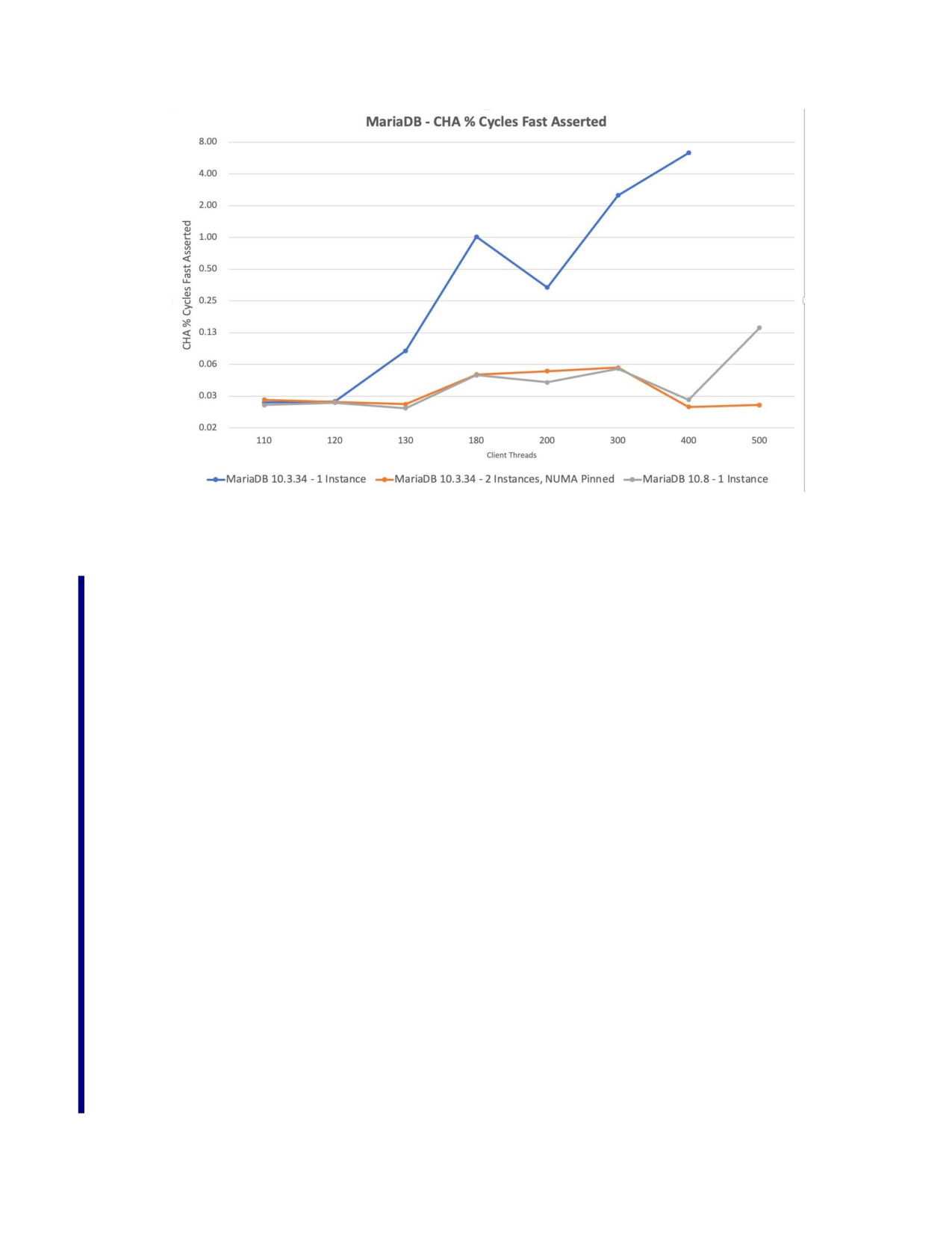
With SysBench/MariaDB 10.3.342, the workload’s throughput drops as the number of threads increases.
Another metric we can use is the CHA% Cycles Fast Asserted. It is a signal to slow down the cores when
the Ingress Queue fills up. This is another way to identify scalability issues. The graph below plots the
number of active client threads representing the work intensity on the horizontal axis. The percentage of
Fast Asserts is plotted on the vertical axis.
The baseline case (blue line) had a sharp throughput with increased thread count, as all cores reduced
their throughput as they suffered from the increasing percent of Fast Asserts. With the same work
distributed instances (red line), Fast asserts dropped. Similarly, with a software fix (gray line), again, the
Fast Asserts dropped even though only one instance was in execution.
1.
2. The most current version is MariaDB 10.3.39
Ref#: 248966-048
3-73
GENERAL OPTIMIZATION GUIDELINES
Figure 3-4. MariaDB - CHA % Cycles Fast Asserted
3.11.5 Scalability With False Sharing
A two-socket 4th Generation Intel® Xeon® Scalable Processors 8480 system can support up to 224
hardware threads (2 sockets x 56 cores per socket x 2 threads per core). However, when multiple threads
concurrently access different variables in a structure that happen to reside in the same cache line, it can
result in false sharing leading to scalability issues. False sharing can cause unnecessary cache invalida-
tions and updates leading to significant performance degradation in multi-threaded programs that utilize
all the hardware threads. Therefore, it is essential to avoid false sharing by designing data structures and
memory layouts that minimize contention on shared cache lines to achieve optimal performance in
multi-threaded environments.
3.11.5.1 Causes of False Sharing
False sharing is a performance problem that can occur in multi-threaded programming when threads
access different variables sharing the same cache line. Cache lines are units of memory that are loaded
into the processor's cache. When multiple threads write different variables in the same cache line, they
end up competing for access to the cache line. This results in cache invalidations and updates that are
unnecessary, which can lead to a significant performance degradation. This problem gets worse when
many threads are contending for the same cache line.
3.11.5.2 Detecting False Sharing
The perf c2c is a profiling tool available in Linux that detects false sharing issues by analyzing
cache-to-cache (c2c) transfers between threads. It works by intercepting the cache coherence messages
sent between threads and identifying the specific cache lines that are involved in false sharing. The perf
c2c approach generates a report that shows the amount of time spent on c2c transfers, the number of
bytes transferred, and the specific cache lines that are affected by false sharing. This approach provides
a more precise and accurate method of detecting false sharing issues compared to traditional profiling
tools, as it directly measures the cache coherence overhead caused by false sharing. The perf c2c
approach is particularly useful for detecting subtle false sharing issues that may not be visible using other
profiling tools.
Ref#: 248966-048
3-74

GENERAL OPTIMIZATION GUIDELINES
Hardware Invalidation Tracking Modified (HITM) is a counter in the perf c2c output that represents the
number of cache lines that were modified in one cache and then invalidated in another cache due to both
false and true sharing. The HITM counter provides insight into the performance impact of false sharing by
measuring the number of unnecessary cache invalidations and the resulting traffic between caches. By
reducing false sharing, the HITM counter can be reduced, leading to better performance and scalability in
multi-threaded programs.
Steps for perf c2c analysis:
1. Collect perf c2c data on the target system (this example is for the full system):
“perf c2c record -a -u --ldlat 50 -- sleep 30
2. Generate report (this can take considerable time to process)
“perf c2c report -NN -g --call-graph --full-symbols -c pid,iaddr --stdio >perf_report.txt
3. Check the generated perf_report.txt for “Shared Data Cache Line Table” (see Table 3-9). This table is
sorted by the HITM. Pay attention to the topped “CacheLine address”. See Example 3-55.
4. Read the perf_report.txt for the “Shared Cache Line Distribution Pareto” (see Table 3-10). Check the
“Offset” column to see if there are multiple offset within single cache line. If there are multiple offset,
that points to a potential false s haring issue. See Example 3-56.
The blog, https://joemario.github.io/blog/2016/09/01/c2c-blog/ , provides a nice introduction to perf
c2c in Linux.
3.11.5.3 Fixing False Sharing and Additional Resources
The following is a list of suggested solutions:
1. Add padding so the fields are not on the same cache line. Example 3-56 shows to prevent the false
sharing between the full and empty lfstack variables padding is added between them. This is the fix
detailed in Section 3.11.5.4. This has the additional effect of increasing the memory sizes and may
create other false sharing for other variables.
2. Run multiple instances of the workload instead of a single instance so that the false sharing for per
in-stance false sharing variables is reduced as fewer hardware threads are allocated per instances.
3. Change other parameters to prevent the false sharing. In the case of Go, the GOGC variable can be
tuned to reduce this.
4. In some environments, it may not be desirable to increase data structure sizes. In this case there
may be other patterns to follow such as splitting up a data structure or changing writes for some
global variable to use compare(read)-then-write instead of unconditional write. However, this will
require further code refactoring.
The Linux kernel has documented some kernel specific False Sharing issues and how to mitigate them.
A blog by a Netflix engineer details how they used a variety of tools including the Intel PMCs (Perfor-
mance Monitoring Counters) to find and fix False Sharing in JVM.
Ref#: 248966-048
3-75

GENERAL OPTIMIZATION GUIDELINES
Example 3-55. Perf Annotation for runtime.getempty
next :* atomic.Load64(&node.next)
6290
425fb6: mov
(%rcx) ,%rdx
// lfstack.go.48
425fb9 lea
0x87fb88(%rip) ,%rbx
9703
425fc0 lock
cmpxchng %rdx,(%rbx)
// lfstack.go.49
425fc5 sete
%dl
425fc8 test
%dl,%dl
425fca je
425f9e <runtime.getempty+0x19e>
425fcc jmp
425fde <runtime.getempty+0x1d0>
425fce xor
%ecx,%ecx
Example 3-56. Padding Insertion in Go Runtime
src/runtime/mgc.go
@@ -285,8 + @@ func pollFractionalWorkerExit() bool {
var work struct {
full l-stack
// lock-free list of full blocks workbuf.
+ pad0 cpu.CacheLinePad
// prevents false-sharing between full and empty.
empty l-stack
// lock-free list of empty blocks workbuf.
3.11.5.4 Case Study: DeathStarBench/hotelReservation
DeathStarBench is an open-source benchmark suite for microservice workloads, originally developed by
Cornell University. It represents different applications written in modern cloud native architecture. The
hotelReservation workload in DeathStarBench mimics a typical microservice workload: a hotel booking
system. It is written in Golang and uses gRPC-go for inter-microservice communication.
When running with the default parameters and on a single instance of the workload, perf c2c shows false
sharing issue with the DSB HR workload. Table 3-10 shows that there are two different offsets being
modified by different threads/functions for the specific cache line.
Table 3-9. Shared Data Cache Line Table
Cache Line
Total
Load Hitm
Index
Address
Node
PA cnt
Hitm
Total
LclHitm
0
0xca5b40
1
19364
3.25%
9083
9083
1
0xd9a840
0
10918
1.66%
4652
4652
2
0xce1140
1
10613
1.56%
4352
4352
3
0xd9a080
0
8300
1.14%
3181
3181
4
0xd9a8c0
0
4274
0.87%
2448
2448
5
0xd95900
0
5346
0.83%
2334
2334
6
0xd9d800
1
5440
0.83%
2324
2324
7
0xce0980
1
6129
0.83%
2319
2319
8
0xd98800
1
5117
0.77%
2160
2160
Ref#: 248966-048
3-76

GENERAL OPTIMIZATION GUIDELINES
Table 3-10. Shared Cache Line Distribution Pareto
HTTM
Data Address
Total
cpu
Shared
RmtHitm
LclHitm
Offset
Node
Symbol
Souce:Line
Records
cnt
Object
0.00%
15.26%
0x0
1
8272
112
[.] runtime.gcDrainN
frontend
mgmark.go:1186
0.00%
8.99%
0x0
1
7276
112
[.] runtime.gcDrain
frontend
mgmark.go:1028
0.00%
7.99%
0x0
1
2850
112
[.] runtime.trygetfull
frontend
lfstack.go.49
0.00%
3.36%
0x0
1
2827
112
[.] runtime.trygetfull
frontend
mgcwork.go.421
0.00%
3.01%
0x0
1
1324
112
[.] runtime.(*lfstack).push
frontend
lfstack.go.35
0.00%
1.94%
0x0
1
885
112
[.] runtime.(*lfstack).push
frontend
lfstack.go.33
0.00%
37.84%
0x8
1
9239
112
[.] runtime.getempty
frontend
lfstack.go.49
0.00%
6.90%
0x8
1
2875
112
[.] runtime.(*lfstack).push
frontend
fstack.go.35
0.00%
5.92%
0x8
1
7188
112
[.] runtime.getempty
frontend
lfstack.go.43
0.00%
4.81%
0x8
1
1947
112
[.] runtime.(*lfstack).push
frontend
lfstack.go.33
0.00%
2.87%
0x8
1
1012
112
[.] runtime.getempty
frontend
mgcwork.go.350
To find the root causes, perf annotate target function:
perf annotate --tui -l -n "runtime.(*lfstack).push
and review the source code to identify false sharing. In this case the update of full and empty lfstack
variables by hardware threads on different cores causes the false sharing.
After identifying and fixing the false sharing problem in the Golang runtime (it is in the Go Runtime),
releasing in and recompiling the workload binary with the modified Golang runtime improved the
throughput metric by 12%. As the following table shows, other metrics such as the CPI and the CHA Fast
Asserts also improve significantly. The perf c2c report also shows no additional false sharing.
Table 3-11. False Sharing Improvements
Metric
False Sharing Fix/Base
TPS
1.12
CPI
0.84
Metric CHA % cycles Fast Asserted
0.42
3.11.6 Instruction Sequence Slowdowns
The Golden Cove CPU microarchitecture upon which the Sapphire Rapids microarchitecture is based has
increased the cost of mixing Legacy SSE and VEX without clearing the state of upper registers for power
efficiency reasons.
3.11.6.1 Causes of Instruction Sequence Slowdowns
The Golden Cove CPU microarchitecture eliminated some hardware speed paths for power efficiency and
replaced them with microcode. The instruction sequence in Table 3-12 mixes VEX and Legacy SSE. It
has, for example, higher core cycles than on the previous generation Sunny Cove CPU microarchitecture
Ref#: 248966-048
3-77

GENERAL OPTIMIZATION GUIDELINES
for the Ice Lake version of the 3rd Generation of Intel® Xeon® Scalable processors. The higher core
cycles are due to the execution of additional micro-operations.
Table 3-12. Instruction Sequence Mixing VEX on the Sapphire Rapids and Ice Lake Server Microarchitectures
Ice lake Server Microarchitecture
Sapphire Rapids Microarchitecture
Intel Assembly Code Syntax
(Sunny Cove Cores)
(Golden Cove Cores)
Inst Retired
Core Cycles
Inst Retired
Core Cycles
VPXOR XMM3, XMM3, XMM3;
VEXTRACTI128 XMM3, YMM3, 1;
PXOR XMM3, XMM3
3.00
1
3.00
388.04
3.11.6.2 Detecting Instruction Sequence Slowdowns
The event ASSISTS.SSE_AVX_MIX can be used to determine if there are VEX to legacy SSE transitions.
The following Linux perf command-line can be used while the workload is running:
$ sudo perf stat -e 'assists.sse_avx_mix’1 <workload>
With the Intel® TMA (Topdown Methodology) (there is a metric called Mixing_Vectors which gives the
percentage of injected blend uops out of all the uops issued. Usually, a Mixing_Vectors metric over 5% is
worth investigating. You can find more details in Appendix B1 of the Optimizations Guide.
3.11.6.3 Fixing Instruction Sequence Slowdowns
The following is a list of suggested solutions:
1. When possible, use VEX-encoded instructions for all the SIMD instructions when possible.
2. Insert a VZEROUPPER to tell the hardware that the state of the higher registers is clean
between the VEX and the legacy SSE instructions. Often the best way to do this is to insert a
VZEROUPPER before returning from any function that uses VEX (that does not produce a VEX
register) and before any call to an unknown function.
VZEROUPPER was inserted in the code sequence below and there are no SSE_AVX_MIX assists. With
this change, the Core Cycles do not have a performance inversion relative to the previous generation.
Table 3-13. Fixed Instruction Sequence with Improved Performance on Sapphire Rapids Microarchitecture
Sapphire Rapids
Ice lake Microarchitecture
ASSISTS.SSE
Intel Assembly Code Syntax
Microarchitecture
(Sunny Cove Cores)
_AVX_MIX
(Golden Cove Cores)
VPXOR XMM3, XMM3, XMM3;
Inst Retired
Core Cycles
Inst Retired
Core Cycles
VEXTRACTI128 XMM3, YMM3, 1;
4.00
2.00
4.00
1.00
0
PXOR XMM3, XMM3
3.11.7 Misprediction for Branches >2GB
The Golden Cove CPU is a wider machine and might exhibit a higher Top-down Microarchitecture Analy-
sis (TMA) Bad Speculation percentage. See Section B.1.1 for additional information about TMA. Some
sources of Bad Speculation are branch prediction misses. In this case, however, Bad Speculation is due
to the wider machine and less efficient branch prediction for certain indirect branches.
1. Using upstream perf. If OS doesn’t have support for the event use
cpu/event=0xc1,umask=0x10,name=assists_sse_avx_mix/
Ref#: 248966-048
3-78

GENERAL OPTIMIZATION GUIDELINES
3.11.7.1 Causes of Branch Misprediction >2GB
For a near absolute indirect JMP/CALL branch instruction (opcodes FF /4 and FF /2), the branch distance
(ADDR_TARGET - ADDR_BRANCH) affects the performance of the branch predictor. The branch predictor
uses fewer resources to predict the branch if its distance can be specified with a 32-bit signed displace-
ment (JMP/CALL imm32). If the distance is larger (>2GB), the predictor uses more resources to predict
the branch and performance may suffer.
3.11.7.2 Detecting Branch Mispredictions >2GB
You can use the Last Branch Record (LBR) to identify jumps greater than 2GB. The collection of perfor-
mance analysis tools based on perf on Linux supports this. The following is an example output from the
tool. It shows that 21% of the call/jumps of >2GB offset are mispredicted. The histogram of one of the
indirect branches at address 0x555555603664 shows that it is to one target and in a library. The profile
mask is to use LBR, and the duration is 10 seconds. It does a system-level profile.
% ./do.py profile --profile-mask=0x100 -s 10
count of indirect call/jump of >2GB offset: 93200
count of mispredicted indirect call/jump of >2GB offset: 19943
misprediction ratio for indirect branch at address 0x7ffff577eca4: 4.23%
misprediction ratio for indirect branch at address 0x5555556030c4: 32.23%
misprediction ratio for indirect branch at address 0x555555603664: 22.30%
misprediction ratio for indirect branch at address 0x555555603c24: 13.84%
…
indirect_0x555555603664 histogram:
0x7ffff7af2670: 50501 100.0%
Figure 3-5. Identifying >2GB Branches
3.11.7.3 Fixing Branch Mispredictions >2GB
Arrange the code so the jumps don’t span the >2GB range. This can be done through a variety of
approaches:
1. If possible, statically link all the libraries into the executable.
2. For .text to library code, use the Glibc environment variable LD_PREFER_MAP_32BIT_EXEC=1 to
restrict the addresses into the 4GB range.
3. For dynamically compiled code, keep it close to the .text address or copy the frequently called entries
into the dynamically compiled code address region. See the Google V8 Blog.
In a case study with WordPress/PHP running eight containers with and without the 2GB fix, the CPI and
performance scores improve by 6%.
Table 3-14. WordPress/PHP Case Study: With and Without a 2GB Fix for Branch Misprediction
WP4.2 / PHP7.4.29
WP4.2 / PHP7.4.29 -
2G FIX/
- NO FIX
2G FIX in Glibc
NO FIX
Workers
8c x 42
8c x 42
-
Cores Per socket
56
56
1.00
Config
Sockets
2
2
1.00
Total Cores
112
112
1.00
Total Thread Count
224
224
1.00
Ref#: 248966-048
3-79

GENERAL OPTIMIZATION GUIDELINES
Table 3-14. WordPress/PHP Case Study: With and Without a 2GB Fix for Branch Misprediction
WP4.2 / PHP7.4.29
WP4.2 / PHP7.4.29 -
2G FIX/
- NO FIX
2G FIX in Glibc
NO FIX
Throughput
1.00
1.06
1.06
Performance
CPI
1.12
1.05
0.96
Path Length
Instructions per Unit of Work
33,789,862.68
33,730,155.10
1.00
Cycles per
Cycles per Unit of Work
37,803,310.48
35,359,628.33
0.94
Transaction
Ref#: 248966-048
3-80
GENERAL OPTIMIZATION GUIDELINES
3.12
OPTIMIZING COMMUNICATION WITH PCI DEVICES ON INTEL® 4TH
GENERATION INTEL® XEON® SCALABLE PROCESSORS
The Sapphire Rapids microarchitecture introduced a new set of instructions designed to optimize
communication between SW running on IA cores and PCI devices on the platform.
3.12.1 Signaling Devices with Direct Move
Most software-to-device interaction follows a producer-to-consumer relationship where the software
creates work for the device and then signals it to inform the device that work is available. Descriptor rings
are the ubiquitous pattern here and once descriptors are added to the ring, the signal (or “doorbell”)
consists of an update to the tail pointer register on the device. This is a write to an MMIO-mapped BAR
register.
Such writes tend to be relatively expensive operations -the latency to complete the write to the device is
high relative to the CPU operating speed. Since writes are ordered by default, this creates a bubble
during which subsequent writes cannot be drained from store buffers. Signaling can therefore affect
performance via store backpressure.
As a result, some software libraries avoid frequent signaling by batching relatively large quantities of
work descriptors with each doorbell update. However, this is not always possible, and it introduces
latency.
The Sapphire Rapids microarchitecture introduces “Direct Store” instructions to optimize signaling; there
are two instructions in the family:
• MOVDIRI: 4/8B direct store.
• MOVDIR64B: 64B atomic direct copy.
Direct Stores are weakly ordered (like non-temporal or USWC-mapped memory writes) regardless of the
underlying memory type (which is usually UC for MMIO-mapped locations). Since they do not order
subsequent writes the performance issue described above does not occur.
Since they are intended for signaling, direct stores will never combine with other stores to the same
address as can happen with non-temporal or USWC writes. Each write is guaranteed to occur as issued.
In the case of MOVDIR64B, the full 64B will be delivered as a single write to the device. This is the only
ISA that carries an architectural guarantee of >8B atomicity.
These instructions benefit from the fact that signaling use cases typically do not care if subsequent writes
are observed before the doorbell itself because the ordering is relaxed. However, since typically the door-
bell must not be observable before earlier writes (such writes are creating the work descriptors), SW
should insert a store fence immediately before the direct store.
Having a fence before the direct store does not normally limit performance- except when many direct
stores are issued. If there is an SFENCE before each, the fence on direct store N+1 imposes an order on
direct store N, which can remove some of the benefits. The guideline is to avoid this where possible. One
technique that may work if multiple doorbells to different addresses are being issued (such as for a NIC
driver that is handling multiple descriptor rings), is to group the direct stores to different locations
together and insert a single SFENCE before the group.
It is also worth noting that the device write latency can vary widely with the address being written. This
is especially true on large CPUs implemented as multiple tiles. So if SW has the luxury of choosing
between multiple addresses, it is possible to envisage adaptive schemes that “match” an address to a SW
thread (especially if that thread is pinned to a single core) by selecting the best performing such address
during an initialization stage.
Ref#: 248966-048
3-81

GENERAL OPTIMIZATION GUIDELINES
3.12.1.1 MOVDIR64B: Additional Considerations
As noted above MOVDIR64B is a copy operation; it moves data from one 64B-aligned address to another.
Typical usage is that the source address is a memory location, and the destination is MMIO mapped to a
device, whereupon it confers the benefits described above. However, since the source data is usually
written immediately before the MOVDIR64B, additional considerations include:
• It is unnecessary to fence to ensure the source data is written before the MOVDIR64B since the
source data is written to the same address that the MOVDIR64B reads. In some scenarios, no store
fence is needed in conjunction with MOVDIR64B. The correct operation of the system depends on
being observed before the MOVDIR64B if no other data is written to memory.
• It is critical to allow store forwarding of the source data for the best performance.
• The source data should be aligned to 64B and written at the same granularity that the MOVDIR64B
reads. For the Sapphire Rapids microarchitecture, this is 64B: the source data should, therefore, be
written using 64B Intel® AVX-512 Instructions for the best performance.
3.12.1.2 Streaming Data
MOVDIR64B can also be used to stream data to a device by copying a block of memory because it is
weakly ordered. This is similar behavior to mapping the destination memory locations as USWC, except:
• The destination address can remain mapped UC.
• The writes are guaranteed to arrive at the device as 64B writes, which is not guaranteed with any
other method.
3.13
SYNCHRONIZATION
3.13.1 User-Level Monitor, User-Level MWAIT, and TPAUSE
New instructions for user-level monitor and MWAIT act like legacy monitor and MWAIT instructions with
additional functionality identified as the timeout and ring-3 (user space) application support. TPAUSE is
similar to legacy pause instruction but is designed to accept time interval and sleep state parameters.
User-level MWAIT and TPAUSE support the same C0.1 light sleep and C0.2 deeper sleep states. These
instructions are helpful in user space applications that support a busy poll, synchronization, or asynchro-
nous IO, such as waiting for an event. A minor code modification yields power benefits along with low
latency wake-up.
3.13.1.1 Checking for User-Level Monitor, MWAIT, and TPAUSE Support
This section describes how to check whether a processor supports user-level monitor, user-level MWAIT,
or TPAUSE; if user-level monitor, user-level MWAIT, or TPAUSE instruction is supported, then CPUID.
(EAX=07H, ECX=0): ECX [bit 5] is enumerated as 1.
Example 3-57. Identification of WAITPKG with CPUID
…identify the existence of cpuid instruction
… ;
… ;
Identify signature is genuine Intel …;
mov eax, 7; Request for feature flags
mov ecx, 0; Request for feature flags
cpuid; 0FH, A2H CPUID instruction
test ecx, 00000020h;
Is waitpkg bit (bit 5) in feature flags equal to 1 jnz Found
Ref#: 248966-048
3-82
GENERAL OPTIMIZATION GUIDELINES
3.13.1.2 User-Level Monitor, User-Level MWAIT, and TPAUSE Operations
User-level monitor initializes the monitor hardware in such a way that, after execution of the user-level
MWAIT, a store to a monitored address acts as a wakeup event. So, the User level monitor and the
user-level MWAIT work together to obtain a sleep state. TPAUSE is a single instruction request to enter
one of the same two sleep states for a defined time
There are possibilities of a “false wake-up” because of other events, notably interrupts or timeouts. The
application may re-execute user-level MWAIT/TPAUSE if it has been falsely woken. If the application
needs to determine the source of the predefined OS sleep wakeup, RFLAGS.CF is set Otherwise it is
assumed that the application can detect changes at the monitored address (MWAIT) or poll for activity
(TPAUSE).
3.13.1.3 Recommended Usage of Monitor, MWAIT, and TPAUSE Operations
A frequent paradigm in packet processing applications is to have dedicated HW threads polling a NIC
receive descriptor ring for ingress traffic. This kind of “busy polling” arrangement wastes energy when
the traffic rates are low. Changing the polling loop to perform user-level Monitor/MWAIT on the next
descriptor to be written can save substantial power in periods of low traffic. The same scheme could be
used with any “work distributor,” assigning work by writing to selected memory locations.
Accelerators frequently offload tasks from SW in an asynchronous manner. For example, the Intel® Data
Streaming Accelerator (Intel® DSA) performs copy operations and can return the status of the completed
operation by writing to memory. If an application uses the user-level monitor/MWAIT at a memory loca-
tion where the status field will be written, it can be woken when the task is complete. Instead of moni-
toring, the device may issue an interrupt that can act as a wake-up event.
Alternatively, applications may decide to choose TPAUSE as a wait event. This has the advantage of being
independent of the number of event sources.
In all cases, a small change in the user space application is needed to convert a busy poll application to
something more energy efficient with low latency wake-up.
Synchronous application: when two hardware threads from the same core use user-level monitor and
user-level MWAIT, it can progress effectively as some of the hardware resources are available to the
other thread when a hyperthread issues the user-level MWAITs.
To achieve the best performance using user-level monitor and user-level MWAIT:
• The entire contents of monitored locations must be verified after user-level MWAIT to avoid a false
wake-up.
• It is the developer’s responsibility to check the contents of monitored locations:
— Before issuing monitor.
— Before issuing user-level MWAIT.
— After user-level MWAIT. See Example 3-58.
• If an application expects a store to a monitored location, the timeout value should be as high as it is
supported.
Ref#: 248966-048
3-83

GENERAL OPTIMIZATION GUIDELINES
Since user-level MWAIT and TPAUSE are a hint to a processor, a user should selectively identify locations
in the application.
Example 3-58. Code Snippet in an Asynchronous Example
void * m_address; // it is expected device will update m_address to 1
unsigned char ret;
while (1) {
if (*m_address != 0) // if device already finished operation, no need to user monitor/user mwait
break;
if (*m_address == 0) { // check monitored location before issuing umonitor instruction
_umonitor (m_address);
if (*m_address == 0) {
// check monitored location before issuing umwait instruction
ret = _umwait(0, 0x186A0);
// some high value in timeout
}
}
}
Ref#: 248966-048
3-84
5.
Updates to Chapter 5
Change bars and violet text show changes to Chapter 5 of the Intel® 64 and IA-32 Architectures Optimization
Resource Manual: Coding for SIMD Architectures.
------------------------------------------------------------------------------------------
Changes to this chapter:
• Section 5.3.1
— Typo correction in Figure 5-4 (Instrinsics to Intrinsics)
Intel® 64 and IA-32 Architectures Optimization Reference Manual Documentation Changes
13

CODING FOR SIMD ARCHITECTURES
CHAPTER 5
CODING FOR SIMD ARCHITECTURES
• Processors based on Intel Core microarchitecture support MMX™, Intel® SSE, Intel® SSE2, Intel®
SSE3, and Intel® SSSE3.
• Processors based on Enhanced Intel Core microarchitecture support MMX, Intel SSE, Intel SSE2,
Intel SSE3, Intel SSSE3, and Intel SSE4.1.
• Processors based on Nehalem microarchitecture support MMX, Intel SSE, Intel SSE2, Intel SSE3,
Intel SSSE3, Intel SSE4.1, and Intel SSE4.2.
• Processors based Westmere microarchitecture support MMX, Intel SSE, Intel SSE2, Intel SSE3, Intel
SSSE3, Intel SSE4.1, Intel SSE4.2, and AESNI.
• Processors based on Sandy Bridge microarchitecture support MMX, Intel SSE, Intel SSE2, Intel SSE3,
Intel SSSE3, Intel SSE4.1, Intel SSE4.2, AESNI, PCLMULQDQ, and Intel® AVX.
• Intel® Pentium® 4, Intel® Xeon® and Intel® Pentium® M processors include support for Intel SSE2,
Intel SSE, and MMX technology. Intel SSE3 was introduced with the Intel Pentium 4 processor
supporting Intel® Hyper-Threading Technology at 90 nm technology.
• Intel® Core™ Solo and Intel® Core™ Duo processors support MMX, Intel SSE, Intel SSE2, and Intel
SSE3.
Single-instruction, multiple-data (SIMD) technologies enable the development of advanced multimedia,
signal processing, and modeling applications.
SIMD techniques can be applied to text/string processing, lexing and parser applications. This is covered
in Chapter 14, “Intel® SSE4.2 and SIMD Programming For Text-Processing/Lexing/Parsing.” Techniques
for optimizing AESNI are discussed in Section 6.10.
To take advantage of the performance opportunities presented by these capabilities, do the following:
• Ensure that the processor supports MMX technology, Intel SSE, Intel SSE2, Intel SSE3, Intel SSSE3,
and Intel SSE4.1.
• Ensure that the operating system supports MMX technology and Intel SSE (OS support for Intel
SSE2, Intel SSE3 and Intel SSSE3 is the same as OS support for Intel SSE).
• Employ the optimization and scheduling strategies described in this book.
• Use stack and data alignment techniques to keep data properly aligned for efficient memory use.
• Utilize the cacheability instructions offered by Intel SSE and Intel SSE2, where appropriate.
5.1
CHECKING FOR PROCESSOR SUPPORT OF SIMD TECHNOLOGIES
This section shows how to check whether a processor supports MMX technology, Intel SSE, Intel SSE2,
Intel SSE3, Intel SSSE3, and Intel SSE4.1.
SIMD technology can be included in your application in three ways:
1. Check for the SIMD technology during installation. If the desired SIMD technology is available, the
appropriate DLLs can be installed.
2. Check for the SIMD technology during program execution and install the proper DLLs at runtime. This
is effective for programs that may be executed on different machines.
3. Create a “fat” binary that includes multiple versions of routines; versions that use SIMD technology
and versions that do not. Check for SIMD technology during program execution and run the
appropriate versions of the routines. This is especially effective for programs that may be executed
on different machines.
Ref#: 248966-047
5-1

CODING FOR SIMD ARCHITECTURES
5.1.1
Checking for MMX Technology Support
If MMX technology is available, then CPUID.01H:EDX[BIT 23] = 1. Use the code segment in Example 5-1
to test for MMX technology.
Example 5-1. Identification of MMX Technology with CPUID
…identify existence of cpuid instruction
…
;
…
; Identify signature is genuine Intel
…
;
mov eax, 1
; Request for feature flags
cpuid
; 0FH, 0A2H CPUID instruction
test edx, 00800000h
; Is MMX technology bit (bit 23) in feature flags equal to 1
jnz
Found
See CPUID Information for Intel® Processors for more information.
5.1.2
Checking for Intel® Streaming SIMD Extensions (Intel® SSE) Support
Checking for processor support of Intel Streaming SIMD Extensions (SIntel SE) on your processor is
similar to checking for MMX technology. However, operating system (OS) must provide support for Intel
SSE states save and restore on context switches to ensure consistent application behavior when using
Intel SSE instructions.
To check whether your system supports Intel SSE, follow these steps:
1. Check that your processor supports the CPUID instruction.
2. Check the feature bits of CPUID for Intel SSE existence.
Example 5-2 shows how to find the SSE feature bit (bit 25) in CPUID feature flags.
Example 5-2. Identification of Intel® SSE with CPUID
…Identify existence of cpuid instruction
; Identify signature is genuine intel
mov eax, 1
; Request for feature flags
cpuid
; 0FH, 0A2H cpuid instruction
test EDX, 002000000h
; Bit 25 in feature flags equal to 1
jnz
Found
5.1.3
Checking for Intel® Streaming SIMD Extensions 2 (Intel® SSE2) Support
Checking for support of Intel SSE2 is like checking for Intel SSE support. The OS requirements for Intel
SSE2 Support are the same as the OS requirements for Intel SSE.
To check whether your system supports Intel SSE2, follow these steps:
1. Check that your processor has the CPUID instruction.
2. Check the feature bits of CPUID for Intel SSE2 technology existence.
Ref#: 248966-047
5-2

CODING FOR SIMD ARCHITECTURES
Example 5-3 shows how to find the SSE2 feature bit (bit 26) in the CPUID feature flags.
Example 5-3. Identification of Intel® SSE2 with cpuid
…identify existence of cpuid instruction
…
; Identify signature is genuine intel
mov eax, 1
; Request for feature flags
cpuid
; 0FH, 0A2H CPUID instruction
test EDX, 004000000h
; Bit 26 in feature flags equal to 1
jnz
Found
5.1.4
Checking for Intel® Streaming SIMD Extensions 3 (Intel® SSE3) Support
Intel SSE3 includes 13 instructions, 11 of those are suited for SIMD or x87 style programming. Checking
for support of Intel SSE3 instructions is similar to checking for Intel SSE support. The OS requirements
for Intel SSE3 Support are the same as the requirements for Intel SSE.
To check whether your system supports the x87 and SIMD instructions of Intel SSE3, follow these steps:
1. Check that your processor has the CPUID instruction.
2. Check the ECX feature bit 0 of CPUID for Intel SSE3 technology existence.
Example 5-4 shows how to find the SSE3 feature bit (bit 0 of ECX) in the CPUID feature flags.
Example 5-4. Identification of Intel® SSE3 with CPUID
…identify existence of cpuid instruction
…
; Identify signature is genuine intel
mov eax, 1
; Request for feature flags
cpuid
; 0FH, 0A2H CPUID instruction
test ECX, 000000001h
; Bit 0 in feature flags equal to 1
jnz
Found
Software must check for support of MONITOR and MWAIT before attempting to use MONITOR and
MWAIT.Detecting the availability of MONITOR and MWAIT can be done using a code sequence similar to
Example 5-4. The availability of MONITOR and MWAIT is indicated by bit 3 of the returned value in ECX.
5.1.5
Checking for Intel® Supplemental Streaming SIMD Extensions 3 (Intel® SSSE)
Support
Checking for support of Intel SSSE3 is similar to checking for Intel SSE support. The OS requirements for
Intel SSSE3 support are the same as the requirements for Intel SSE.
To check whether your system supports Intel SSSE3, follow these steps:
1. Check that your processor has the CPUID instruction.
2. Check the feature bits of CPUID for Intel SSSE3 technology existence.
Example 5-5 shows how to find the Intel SSSE3 feature bit in the CPUID feature flags.
Example 5-5. Identification of SSSE3 with cpuid
…Identify existence of CPUID instruction
…
; Identify signature is genuine intel
mov eax, 1
; Request for feature flags
cpuid
; 0FH, 0A2H CPUID instruction
test ECX, 000000200h
; ECX bit 9
jnz
Found
Ref#: 248966-047
5-3

CODING FOR SIMD ARCHITECTURES
5.1.6
Checking for Intel® SSE4.1 Support
Checking for support of SSE4.1 is similar to checking for Intel SSE support. The OS requirements for Intel
SSE4.1 support are the same as the requirements for Intel SSE.
To check whether your system supports Intel SSE4.1, follow these steps:
1. Check that your processor has the CPUID instruction.
2. Check the feature bit of CPUID for Intel SSE4.1.
Example 5-6 shows how to find the Intel SSE4.1 feature bit in the CPUID feature flags.
Example 5-6. Identification of Intel® SSE4.1 with CPUID
…Identify existence of CPUID instruction
…
; Identify signature is genuine intel
mov eax, 1
; Request for feature flags
cpuid
; 0FH, 0A2H CPUID instruction
test ECX, 000080000h
; ECX bit 19
jnz
Found
5.1.7
Checking for Intel® SSE4.2 Support
Checking for support of Intel SSE4.2 is similar to checking for Intel SSE support. The OS requirements for
SSE4.2 support are the same as the requirements for Intel SSE.
To check whether your system supports SSE4.2, follow these steps:
1. Check that your processor has the CPUID instruction.
2. Check the feature bit of CPUID for Intel SSE4.2.
Example 5-7 shows how to find the INtel SSE4.2 feature bit in the CPUID feature flags.
Example 5-7. Identification of SSE4.2 with cpuid
…Identify existence of CPUID instruction
…
; Identify signature is genuine intel
mov eax, 1
; Request for feature flags
cpuid
; 0FH, 0A2H CPUID instruction
test ECX, 000100000h
; ECX bit 20
jnz
Found
5.1.8
DetectiON of PCLMULQDQ and AESNI Instructions
Before an application attempts to use the following AESNI instructions: AESDEC/AESDE-
CLAST/AESENC/AESENCLAST/AESIMC/AESKEYGENASSIST, it must check that the processor supports
the AESNI extensions. AESNI extensions is supported if CPUID.01H:ECX.AESNI[bit 25] = 1.
Prior to using PCLMULQDQ instruction, application must check if CPUID.01H:ECX.PCLMULQDQ[bit 1] = 1.
Ref#: 248966-047
5-4

CODING FOR SIMD ARCHITECTURES
Operating systems that support handling SSE state will also support applications that use AESNI exten-
sions and PCLMULQDQ instruction. This is the same requirement for Intel SSE2, Intel SSE3, Intel SSSE3,
and Intel SSE4.
Example 5-8. Detection of AESNI Instructions
…Identify existence of CPUID instruction
…
; Identify signature is genuine intel
mov eax, 1
; Request for feature flags
cpuid
; 0FH, 0A2H CPUID instruction
test ECX, 002000000h
; ECX bit 25
jnz
Found
Example 5-9. Detection of PCLMULQDQ Instruction
…Identify existence of CPUID instruction
…
; Identify signature is genuine intel
mov eax, 1
; Request for feature flags
cpuid
; 0FH, 0A2H CPUID instruction
test ECX, 000000002h
; ECX bit 1
jnz
Found
5.1.9
Detection of Intel® AVX Instructions
Intel AVX operates on the 256-bit YMM register state. Application detection of new instruction extensions
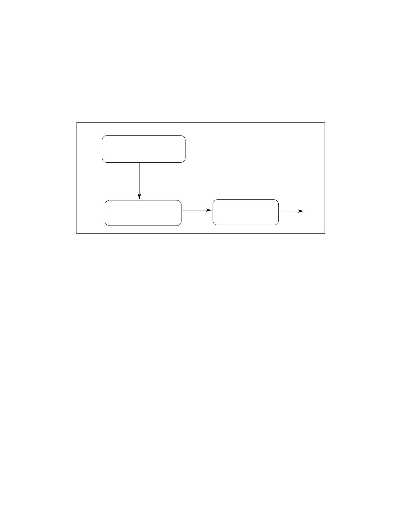
operating on the YMM state follows the general procedural flow in Figure 5-1.
Prior to using AVX, the application must identify that the operating system supports the XGETBV instruc-
tion, the YMM register state, in addition to processor’s support for YMM state management using
XSAVE/XRSTOR and AVX instructions. The following simplified sequence accomplishes both and is
strongly recommended.
1) Detect CPUID.1:ECX.OSXSAVE[bit 27] = 1 (XGETBV enabled for application use1)
2) Issue XGETBV and verify that XFEATURE_ENABLED_MASK[2:1] = ‘11b’ (XMM state and YMM state are
enabled by OS).
3) Detect CPUID.1:ECX.AVX[bit 28] = 1 (AVX instructions supported).
Note: Step 3 can be done in any order relative to 1 and 2.
1.If CPUID.01H:ECX.OSXSAVE reports 1, it also indirectly implies the processor supports XSAVE, XRSTOR, XGETBV, proces-
sor extended state bit vector XFEATURE_ENALBED_MASK register. Thus an application may streamline the checking of
CPUID feature flags for XSAVE and OSXSAVE. XSETBV is a privileged instruction.
Ref#: 248966-047
5-5

CODING FOR SIMD ARCHITECTURES
Check feature flag
CPUID.1H:ECX.OXSAVE = 1?
OS provides processor
Yes
extended state management
Implied HW support for
XSAVE, XRSTOR, XGETBV, XFEATURE_ENABLED_MASK
Check enabled state in
Check feature flag
State
for Instruction set
ok to use
XCR0 via XGETBV
enabled
Instructions
Figure 5-1. General Procedural Flow of Application Detection of Intel® AVX
The following pseudocode illustrates this recommended application Intel AVX detection process:
Example 5-10. Detection of Intel® AVX Instruction
INT supports_AVX()
{
mov
eax, 1
cpuid
and
ecx, 018000000H
cmp
ecx, 018000000H; check both OSXSAVE and AVX feature flags
jne
not_supported
; processor supports AVX instructions and XGETBV is enabled by OS
mov
ecx, 0; specify 0 for XFEATURE_ENABLED_MASK register
XGETBV
; result in EDX:EAX
and
eax, 06H
cmp
eax, 06H; check OS has enabled both XMM and YMM state support
jne
not_supported
mov
eax, 1
jmp
done
NOT_SUPPORTED:
mov
eax, 0
done:
NOTE
It is unwise for an application to rely exclusively on CPUID.1:ECX.AVX[bit 28] or at all on
CPUID.1:ECX.XSAVE[bit 26]: These indicate hardware support but not operating system
support. If YMM state management is not enabled by an operating systems, AVX instruc-
tions will #UD regardless of CPUID.1:ECX.AVX[bit 28]. “CPUID.1:ECX.XSAVE[bit 26] =
1” does not guarantee the OS actually uses the XSAVE process for state management.
Ref#: 248966-047
5-6

CODING FOR SIMD ARCHITECTURES
5.1.10 Detection of VEX-Encoded AES and VPCLMULQDQ
VAESDEC/VAESDECLAST/VAESENC/VAESENCLAST/VAESIMC/VAESKEYGENASSIST instructions operate
on YMM states. The detection sequence must combine checking for CPUID.1:ECX.AES[bit 25] = 1 and
the sequence for detection application support for Intel AVX.
Example 5-11. Detection of VEX-Encoded AESNI Instructions
INT supports_VAESNI()
{
mov
eax, 1
cpuid
and
ecx, 01A000000H
cmp
ecx, 01A000000H; check OSXSAVE AVX and AESNI feature flags
jne
not_supported
; processor supports AVX and VEX-encoded AESNI and XGETBV is enabled by OS
mov
ecx, 0; specify 0 for XFEATURE_ENABLED_MASK register
XGETBV
; result in EDX:EAX
and
eax, 06H
cmp
eax, 06H; check OS has enabled both XMM and YMM state support
jne
not_supported
mov
eax, 1
jmp
done
NOT_SUPPORTED:
mov
eax, 0
done:
Similarly, the detection sequence for VPCLMULQDQ must combine checking for
CPUID.1:ECX.PCLMULQDQ[bit 1] = 1 and the sequence for detection application support for AVX.
This is shown in the pseudocode:
Example 5-12. Detection of VEX-Encoded AESNI Instructions
INT supports_VPCLMULQDQ)
{
mov
eax, 1
cpuid
and
ecx, 018000002H
cmp
ecx, 018000002H; check OSXSAVE AVX and PCLMULQDQ feature flags
jne
not_supported
; processor supports AVX and VEX-encoded PCLMULQDQ and XGETBV is enabled by OS
mov
ecx, 0; specify 0 for XFEATURE_ENABLED_MASK register
XGETBV
; result in EDX:EAX
and
eax, 06H
cmp
eax, 06H; check OS has enabled both XMM and YMM state support
jne
not_supported
mov
eax, 1
jmp
done
NOT_SUPPORTED:
mov
eax, 0
done:
Ref#: 248966-047
5-7
CODING FOR SIMD ARCHITECTURES
5.1.11 Detection of F16C Instructions
Application using float 16 instruction must follow a detection sequence similar to Intel AVX to ensure:
• The OS has enabled YMM state management support.
• The processor support Intel AVX as indicated by the CPUID feature flag, i.e. CPUID.01H:ECX.AVX[bit
28] = 1.
• The processor support 16-bit floating-point conversion instructions via a CPUID feature flag
(CPUID.01H:ECX.F16C[bit 29] = 1).
Application detection of Float-16 conversion instructions follow the general procedural flow in Figure 5-2.
Check feature flag
CPUID.1H:ECX.OXSAVE = 1?
Yes
OS provides processor
extended state management
Implied HW support for
XSAVE, XRSTOR, XGETBV, XFEATURE_ENABLED_MASK
Check enabled YMM state in
Check feature flags
XCR0 via XGETBV
State
for AVX and F16C
ok to use
enabled
Instructions
Figure 5-2. General Procedural Flow of Application Detection of Float-16
----------------------------------------------------------------------------------------
INT supports_f16c()
{
; result in eax
mov eax, 1
cpuid
and ecx, 038000000H
cmp ecx, 038000000H; check OSXSAVE, AVX, F16C feature flags
jne not_supported
; processor supports AVX,F16C instructions and XGETBV is enabled by OS
mov ecx, 0; specify 0 for XFEATURE_ENABLED_MASK register
XGETBV; result in EDX:EAX
and eax, 06H
cmp eax, 06H; check OS has enabled both XMM and YMM state support
jne not_supported
mov eax, 1
jmp done
NOT_SUPPORTED:
mov eax, 0
done:
}
-------------------------------------------------------------------------------
Ref#: 248966-047
5-8
CODING FOR SIMD ARCHITECTURES
5.1.12 Detection of FMA
Hardware support for FMA is indicated by CPUID.1:ECX.FMA[bit 12]=1.
Application Software must identify that hardware supports AVX, after that it must also detect support for
FMA by CPUID.1:ECX.FMA[bit 12]. The recommended pseudocode sequence for detection of FMA is:
----------------------------------------------------------------------------------------
INT supports_fma()
{
; result in eax
mov eax, 1
cpuid
and ecx, 018001000H
cmp ecx, 018001000H; check OSXSAVE, AVX, FMA feature flags
jne not_supported
; processor supports AVX,FMA instructions and XGETBV is enabled by OS
mov ecx, 0; specify 0 for XFEATURE_ENABLED_MASK register
XGETBV; result in EDX:EAX
and eax, 06H
cmp eax, 06H; check OS has enabled both XMM and YMM state support
jne not_supported
mov eax, 1
jmp done
NOT_SUPPORTED:
mov eax, 0
done:
}
-------------------------------------------------------------------------------
5.1.13 Detection of Intel® AVX2
Hardware support for Intel AVX2 is indicated by CPUID.(EAX=07H, ECX=0H):EBX.AVX2[bit 5]=1.
Application Software must identify that hardware supports Intel AVX, after that it must also detect
support for AVX2 by checking CPUID.(EAX=07H, ECX=0H):EBX.AVX2[bit 5]. The recommended pseudo-
code sequence for detection of Intel AVX2 is:
----------------------------------------------------------------------------------------
INT supports_avx2()
{
; result in eax
mov eax, 1
cpuid
and ecx, 018000000H
cmp ecx, 018000000H; check both OSXSAVE and AVX feature flags
jne not_supported
; processor supports AVX instructions and XGETBV is enabled by OS
mov eax, 7
mov ecx, 0
cpuid
Ref#: 248966-047
5-9
CODING FOR SIMD ARCHITECTURES
and ebx, 20H
cmp ebx, 20H; check AVX2 feature flags
jne not_supported
mov ecx, 0; specify 0 for XFEATURE_ENABLED_MASK register
XGETBV; result in EDX:EAX
and eax, 06H
cmp eax, 06H; check OS has enabled both XMM and YMM state support
jne not_supported
mov eax, 1
jmp done
NOT_SUPPORTED:
mov eax, 0
done:
}
-------------------------------------------------------------------------------
5.2
CONSIDERATIONS FOR CODE CONVERSION TO SIMD
PROGRAMMING
The VTune Performance Enhancement Environment CD provides tools to aid in the evaluation and tuning.
Before implementing them, you need answers to the following questions:
1. Will the current code benefit by using MMX technology, Intel SSE, Intel SSE2, Intel SSE3, or Intel
SSSE3?
2. Is this code integer or floating-point?
3. What integer word size or floating-point precision is needed?
4. What coding techniques should I use?
5. What guidelines do I need to follow?
6. How should I arrange and align the datatypes?
Figure 5-3 provides a flowchart for the process of converting code to MMX technology, Intel SSE, Intel
SSE2, Intel SSE3, or Intel SSSE3.
Ref#: 248966-047
5-10
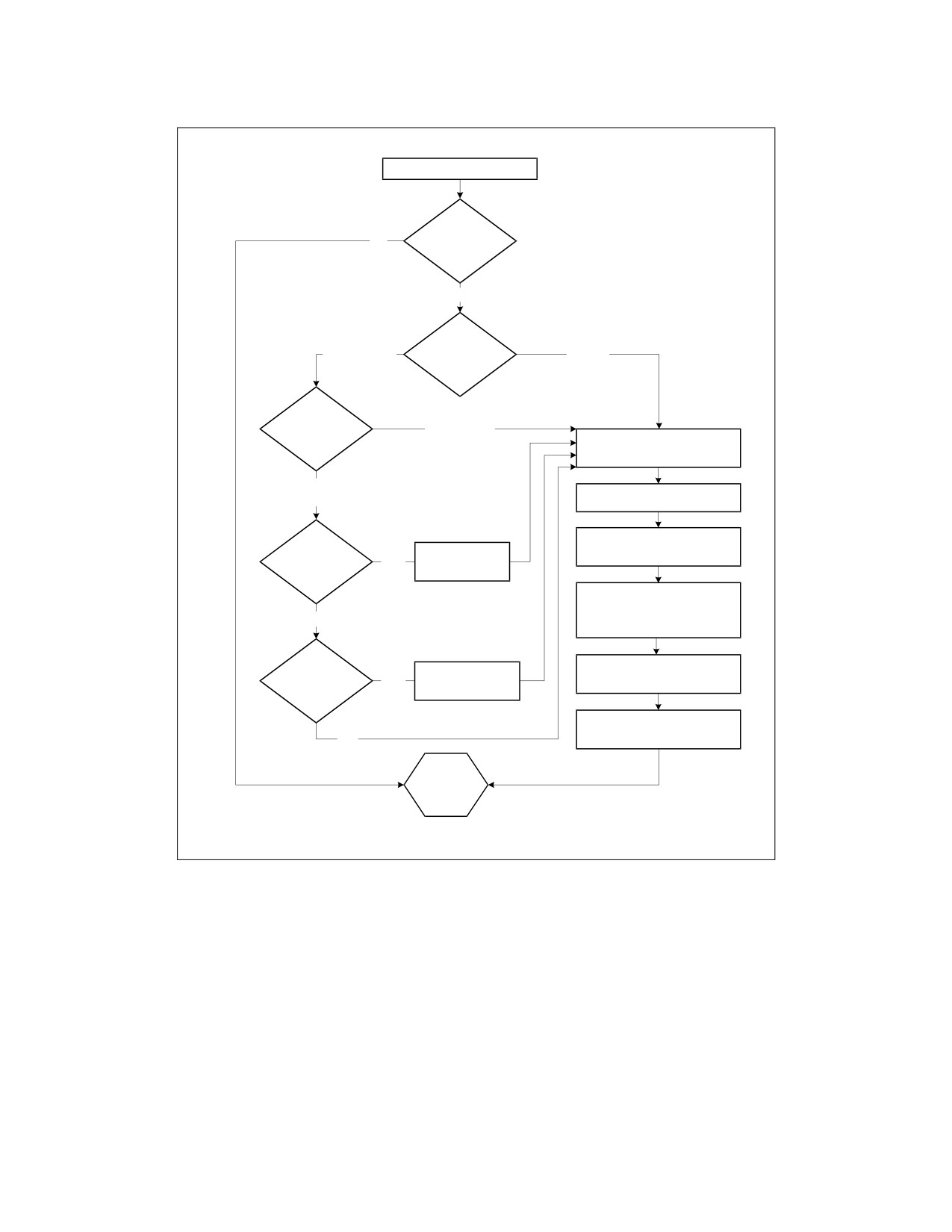
CODING FOR SIMD ARCHITECTURES
Identify Hot Spots in Code
Code benefits
No
from SIMD
Yes
Integer or
Floating Point
Integer
floating-point?
Why FP?
Performance
If possible, re-arrange data
for SIMD efficiency
Range or
Precision
Align data structures
Convert to code to use
Can convert
Change to use
SIMD Technologies
Yes
to Integer?
SIMD Integer
Follow general coding
guidelines and SIMD
No
coding guidelines
Use memory optimizations
Can convert to
Change to use
Yes
and prefetch if appropriate
Single-precision?
Single Precision
Schedule instructions to
No
optimize performance
STOP
OM15156
Figure 5-3. Converting to Intel® Streaming SIMD Extensions Chart
To use any of the SIMD technologies optimally, you must evaluate the following situations in your code:
• Fragments that are computationally intensive.
• Fragments that are executed often enough to have an impact on performance.
• Fragments that with little data-dependent control flow.
• Fragments that require floating-point computations.
• Fragments that can benefit from moving data 16 bytes at a time.
• Fragments of computation that can coded using fewer instructions.
• Fragments that require help in using the cache hierarchy efficiently.
Ref#: 248966-047
5-11
CODING FOR SIMD ARCHITECTURES
5.2.1
Identifying Hot Spots
To optimize performance, use the VTune Performance Analyzer to find sections of code that occupy most
of the computation time. Such sections are called the hotspots. See Appendix A, “Application Perfor-
mance Tools.”
The VTune analyzer provides a hotspots view of a specific module to help you identify sections in your
code that take the most CPU time and that have potential performance problems. The hotspots view
helps you identify sections in your code that take the most CPU time and that have potential performance
problems.
The VTune analyzer enables you to change the view to show hotspots by memory location, functions,
classes, or source files. You can double-click on a hotspot and open the source or assembly view for the
hotspot and see more detailed information about the performance of each instruction in the hotspot.
The VTune analyzer offers focused analysis and performance data at all levels of your source code and
can also provide advice at the assembly language level. The code coach analyzes and identifies opportu-
nities for better performance of C/C++, Fortran and Java* programs, and suggests specific optimiza-
tions. Where appropriate, the coach displays pseudo-code to suggest the use of highly optimized
intrinsics and functions in the Intel® Performance Library Suite. Because VTune analyzer is designed
specifically for Intel architecture (IA)-based processors, including the Pentium 4 processor, it can offer
detailed approaches to working with IA. See Appendix A.1.1 for details.
5.2.2
Determine If Code Benefits by Conversion to SIMD Execution
Identifying code that benefits by using SIMD technologies can be time-consuming and difficult. Likely
candidates for conversion are applications that are highly computation intensive, such as the following:
• Speech compression algorithms and filters.
• Speech recognition algorithms.
• Video display and capture routines.
• Rendering routines.
•
3D graphics (geometry).
• Image and video processing algorithms.
• Spatial (3D) audio.
• Physical modeling (graphics, CAD).
• Workstation applications.
• Encryption algorithms.
• Complex arithmetics.
Generally, good candidate code is code that contains small-sized repetitive loops that operate on sequen-
tial arrays of integers of 8, 16 or 32 bits, single-precision 32-bit floating-point data, double precision 64-
bit floating-point data (integer and floating-point data items should be sequential in memory). The repet-
itiveness of these loops incurs costly application processing time. However, these routines have potential
for increased performance when you convert them to use one of the SIMD technologies.
Once you identify your opportunities for using a SIMD technology, you must evaluate what should be
done to determine whether the current algorithm or a modified one will ensure the best performance.
Ref#: 248966-047
5-12
CODING FOR SIMD ARCHITECTURES
5.3
CODING TECHNIQUES
The SIMD features of Intel SSE3, Intel SSE2, Intel SSE, and MMX technology require new methods of
coding algorithms. One of them is vectorization. Vectorization is the process of transforming sequen-
tially-executing, or scalar, code into code that can execute in parallel, taking advantage of the SIMD
architecture parallelism. This section discusses the coding techniques available for an application to
make use of the SIMD architecture.
To vectorize your code and thus take advantage of the SIMD architecture, do the following:
• Determine if the memory accesses have dependencies that would prevent parallel execution.
•
“Strip-mine” the inner loop to reduce the iteration count by the length of the SIMD operations (for
example, four for single-precision floating-point SIMD, eight for 16-bit integer SIMD on the XMM
registers).
• Re-code the loop with the SIMD instructions.
Each of these actions is discussed in detail in the subsequent sections of this chapter. These sections also
discuss enabling automatic vectorization using the Intel C++ Compiler.
5.3.1
Coding Methodologies
Software developers need to compare the performance improvement that can be obtained from
assembly code versus the cost of those improvements. Programming directly in assembly language for a
target platform may produce the required performance gain, however, assembly code is not portable
between processor architectures and is expensive to write and maintain.
Performance objectives can be met by taking advantage of the different SIMD technologies using high-
level languages as well as assembly. The new C/C++ language extensions designed specifically for Intel
SSE3, Intel SSE2, Intel SSE, and MMX technology help make this possible.
Figure 5-4 illustrates the trade-offs involved in the performance of hand-coded assembly versus the ease
of programming and portability.
Assembly
Intrinsics
Automatic
Vectoriztion
C/C++ / Fortran
Ease of Programming/Portability
Figure 5-4. Hand-Coded Assembly and High-Level Compiler Performance Trade-Offs
Ref#: 248966-047
5-13

CODING FOR SIMD ARCHITECTURES
The examples that follow illustrate the use of coding adjustments to enable the algorithm to benefit from
the Intel SSE. The same techniques may be used for single-precision floating-point, double-precision
floating-point, and integer data under Intel SSE3, Intel SSE2, Intel SSE, and MMX technology.
As a basis for the usage model discussed in this section, consider a simple loop shown in Example 5-13.
Example 5-13. Simple Four-Iteration Loop
void add(float *a, float *b, float *c)
{
int i;
for (i = 0; i < 4; i++) {
c[i] = a[i] + b[i];
}
}
Note that the loop runs for only four iterations. This allows a simple replacement of the code with
Streaming SIMD Extensions.
For the optimal use of the Intel SSE that need data alignment on the 16-byte boundary, all examples in
this chapter assume that the arrays passed to the routine, A, B, C, are aligned to 16-byte boundaries by
a calling routine. For the methods to ensure this alignment, please refer to the application notes for the
Intel Pentium 4 processor.
The sections that follow provide details on the coding methodologies: inlined assembly, intrinsics, C++
vector classes, and automatic vectorization.
5.3.1.1
Assembly
Key loops can be coded directly in assembly language using an assembler or by using inlined assembly
(C-asm) in C/C++ code. The Intel compiler or assembler recognize the new instructions and registers,
then directly generate the corresponding code. This model offers the opportunity for attaining greatest
performance, but this performance is not portable across the different processor architectures.
Example 5-14 shows the Intel SSE inlined assembly encoding.
Example 5-14. Intel® Streaming SIMD Extensions (Intel® SSE) Using Inlined Assembly Encoding
void add(float *a, float *b, float *c)
{
__asm {
mov eax, a
mov edx, b
mov ecx, c
movaps xmm0, XMMWORD PTR [eax]
addps xmm0, XMMWORD PTR [edx]
movaps XMMWORD PTR [ecx], xmm0
}
}
5.3.1.2
Intrinsics
Intrinsics provide the access to the ISA functionality using C/C++ style coding instead of assembly
language. Intel has defined three sets of intrinsic functions that are implemented in the Intel C++
Compiler to support the MMX technology, Intel SSE, Intel SSE2. Four new C data types, representing 64-
bit and 128-bit objects are used as the operands of these intrinsic functions. __M64 is used for MMX
integer SIMD, __M128 is used for single-precision floating-point SIMD, __M128I is used for Streaming
SIMD Extensions 2 integer SIMD, and __M128D is used for double precision floating-point SIMD. These
Ref#: 248966-047
5-14

CODING FOR SIMD ARCHITECTURES
types enable the programmer to choose the implementation of an algorithm directly, while allowing the
compiler to perform register allocation and instruction scheduling where possible. The intrinsics are
portable among all Intel architecture-based processors supported by a compiler.
The use of intrinsics allows you to obtain performance close to the levels achievable with assembly. The
cost of writing and maintaining programs with intrinsics is considerably less. For a detailed description of
the intrinsics and their use, refer to the Intel C++ Compiler documentation.
Example 5-15 shows the loop from Example 5-13 using intrinsics.
Example 5-15. Simple Four-Iteration Loop Coded with Intrinsics
#include <xmmintrin.h>
void add(float *a, float *b, float *c)
{
__m128 t0, t1;
t0 = _mm_load_ps(a);
t1 = _mm_load_ps(b);
t0 = _mm_add_ps(t0, t1);
_mm_store_ps(c, t0);
}
The intrinsics map one-to-one with actual Intel SSE assembly code. The XMMINTRIN.H header file in
which the prototypes for the intrinsics are defined is part of the Intel C++ Compiler included with the
VTune Performance Enhancement Environment CD.
Intrinsics are also defined for the MMX technology ISA. These are based on the __m64 data type to
represent the contents of an mm register. You can specify values in bytes, short integers, 32-bit values,
or as a 64-bit object.
The intrinsic data types, however, are not a basic ANSI C data type, and therefore you must observe the
following usage restrictions:
• Use intrinsic data types only on the left-hand side of an assignment as a return value or as a
parameter. You cannot use it with other arithmetic expressions (for example, “+”, “>>”).
• Use intrinsic data type objects in aggregates, such as unions to access the byte elements and
structures; the address of an __M64 object may be also used.
• Use intrinsic data type data only with the MMX technology intrinsics described in this guide.
For complete details of the hardware instructions, see the Intel Architecture MMX Technology
Developer’s Guide. For a description of data types, see the Intel® 64 and IA-32 Architectures Software
Developer’s Manual.
5.3.1.3
Classes
A set of C++ classes has been defined and available in Intel C++ Compiler to provide both a higher-level
abstraction and more flexibility for programming with MMX technology, Intel SSE and Intel SSE2. These
classes provide an easy-to-use and flexible interface to the intrinsic functions, allowing developers to
write more natural C++ code without worrying about which intrinsic or assembly language instruction to
use for a given operation. Since the intrinsic functions underlie the implementation of these C++ classes,
the performance of applications using this methodology can approach that of one using the intrinsics.
Further details on the use of these classes can be found in the Intel C++ Class Libraries for SIMD Opera-
tions page.
Ref#: 248966-047
5-15

CODING FOR SIMD ARCHITECTURES
Example 5-16 shows the C++ code using a vector class library. The example assumes the arrays passed
to the routine are already aligned to 16-byte boundaries.
Example 5-16. C++ Code Using the Vector Classes
#include <fvec.h>
void add(float *a, float *b, float *c)
{
F32vec4 *av=(F32vec4 *) a;
F32vec4 *bv=(F32vec4 *) b;
F32vec4 *cv=(F32vec4 *) c;
*cv=*av + *bv;
}
Here, fvec.h is the class definition file and F32vec4 is the class representing an array of four floats. The
“+” and “=” operators are overloaded so that the actual Streaming SIMD Extensions implementation in
the previous example is abstracted out, or hidden, from the developer. Note how much more this resem-
bles the original code, allowing for simpler and faster programming.
Again, the example is assuming the arrays, passed to the routine, are already aligned to 16-byte
boundary.
5.3.1.4
Automatic Vectorization
The Intel C++ Compiler provides an optimization mechanism by which loops, such as in Example 5-13
can be automatically vectorized, or converted into Intel SSE code. The compiler uses similar techniques
to those used by a programmer to identify whether a loop is suitable for conversion to SIMD. This
involves determining whether the following might prevent vectorization:
• The layout of the loop and the data structures used.
• Dependencies amongst the data accesses in each iteration and across iterations.
Once the compiler has made such a determination, it can generate vectorized code for the loop, allowing
the application to use the SIMD instructions.
The caveat to this is that only certain types of loops can be automatically vectorized, and in most cases
user interaction with the compiler is needed to fully enable this.
Example 5-17 shows the code for automatic vectorization for the simple four-iteration loop (from
Example 5-13).
Example 5-17. Automatic Vectorization for a Simple Loop
void add (float *restrict a,
float *restrict b,
float *restrict c)
{
int i;
for (i = 0; i < 4; i++) {
c[i] = a[i] + b[i];
}
}
Compile this code using the -QAX and -QRESTRICT switches of the Intel C++ Compiler, version 4.0 or
later.
The RESTRICT qualifier in the argument list is necessary to let the compiler know that there are no other
aliases to the memory to which the pointers point. In other words, the pointer for which it is used,
Ref#: 248966-047
5-16
CODING FOR SIMD ARCHITECTURES
provides the only means of accessing the memory in question in the scope in which the pointers live.
Without the restrict qualifier, the compiler will still vectorize this loop using runtime data dependence
testing, where the generated code dynamically selects between sequential or vector execution of the
loop, based on overlap of the parameters. The restrict keyword avoids the associated overhead alto-
gether.
See Intel® C++ Compiler Classic Developer Guide and Reference for details.
5.4
STACK AND DATA ALIGNMENT
To get the most performance out of code written for SIMD technologies data should be formatted in
memory according to the guidelines described in this section. Assembly code with an unaligned accesses
is a lot slower than an aligned access.
5.4.1
Alignment and Contiguity of Data Access Patterns
The 64-bit packed data types defined by MMX technology, and the 128-bit packed data types for Intel
SSE and Intel SSE2 create more potential for misaligned data accesses. The data access patterns of
many algorithms are inherently misaligned when using MMX technology and SSE. Several techniques for
improving data access, such as padding, organizing data elements into arrays, etc. are described below.
Intel SSE3 provides a special-purpose instruction LDDQU that can avoid cache line splits is discussed in
Section 6.7.3
5.4.1.1
Using Padding to Align Data
However, when accessing SIMD data using SIMD operations, access to data can be improved simply by a
change in the declaration. For example, consider a declaration of a structure, which represents a point in
space plus an attribute.
typedef struct {short x,y,z; char a} Point;
Point pt[N];
Assume we will be performing a number of computations on X, Y, Z in three of the four elements of a
SIMD word; see Section 5.5.1 for an example. Even if the first element in array PT is aligned, the second
element will start 7 bytes later and not be aligned (3 shorts at two bytes each plus a single byte = 7
bytes).
By adding the padding variable PAD, the structure is now 8 bytes, and if the first element is aligned to 8
bytes (64 bits), all following elements will also be aligned. The sample declaration follows:
typedef struct {short x,y,z; char a; char pad;} Point;
Point pt[N];
5.4.1.2
Using Arrays to Make Data Contiguous
In the following code,
for (i=0; i<N; i++) pt[i].y *= scale;
the second dimension Y needs to be multiplied by a scaling value. Here, the FOR loop accesses each Y
dimension in the array PT thus disallowing the access to contiguous data. This can degrade the perfor-
mance of the application by increasing cache misses, by poor utilization of each cache line that is fetched,
and by increasing the chance for accesses which span multiple cache lines.
The following declaration allows you to vectorize the scaling operation and further improve the alignment
of the data access patterns:
short ptx[N], pty[N], ptz[N];
for (i=0; i<N; i++) pty[i] *= scale;
Ref#: 248966-047
5-17

CODING FOR SIMD ARCHITECTURES
With the SIMD technology, choice of data organization becomes more important and should be made
carefully based on the operations that will be performed on the data. In some applications, traditional
data arrangements may not lead to the maximum performance.
A simple example of this is an FIR filter. An FIR filter is effectively a vector dot product in the length of the
number of coefficient taps.
Consider the following code:
(data [ j ] *coeff [0] + data [j+1]*coeff [1]+...+data [j+num of taps-1]*coeff [num of taps-1]),
If in the code above the filter operation of data element I is the vector dot product that begins at data
element J, then the filter operation of data element I+1 begins at data element J+1.
Assuming you have a 64-bit aligned data vector and a 64-bit aligned coefficients vector, the filter opera-
tion on the first data element will be fully aligned. For the second data element, however, access to the
data vector will be misaligned. For an example of how to avoid the misalignment problem in the FIR filter,
refer to Intel application notes on Streaming SIMD Extensions and filters.
Duplication and padding of data structures can be used to avoid the problem of data accesses in algo-
rithms which are inherently misaligned. Section 5.5.1 discusses trade-offs for organizing data structures.
NOTE
The duplication and padding technique overcomes the misalignment problem, thus
avoiding the expensive penalty for misaligned data access, at the cost of increasing the
data size. When developing your code, you should consider this tradeoff and use the
option which gives the best performance.
5.4.2
Stack Alignment for 128-bit SIMD Technologies
For best performance, the Streaming SIMD Extensions and Streaming SIMD Extensions 2 require their
memory operands to be aligned to 16-byte boundaries. Unaligned data can cause significant perfor-
mance penalties compared to aligned data. However, the existing software conventions for IA-32
(STDCALL, CDECL, FASTCALL) as implemented in most compilers, do not provide any mechanism for
ensuring that certain local data and certain parameters are 16-byte aligned. Therefore, Intel has defined
a new set of IA-32 software conventions for alignment to support the new __M128* datatypes (__M128,
__M128D, and __M218I). These meet the following conditions:
• Functions that use Streaming SIMD Extensions or Streaming SIMD Extensions 2 data need to provide
a 16-byte aligned stack frame.
•
__M128* parameters need to be aligned to 16-byte boundaries, possibly creating “holes” (due to
padding) in the argument block.
The new conventions presented in this section as implemented by the Intel C++ Compiler can be used as
a guideline for an assembly language code as well. In many cases, this section assumes the use of the
__M128* data types, as defined by the Intel C++ Compiler, which represents an array of four 32-bit floats.
5.4.3
Data Alignment for MMX™ Technology
Many compilers enable alignment of variables using controls. This aligns variable bit lengths to the
appropriate boundaries. If some of the variables are not appropriately aligned as specified, you can align
them using the C algorithm in Example 5-18.
Example 5-18. C Algorithm for 64-bit Data Alignment
/* Make newp a pointer to a 64-bit aligned array of NUM_ELEMENTS 64-bit elements. */
double *p, *newp;
p = (double*)malloc (sizeof(double)*(NUM_ELEMENTS+1));
newp = (p+7) & (~0x7);
Ref#: 248966-047
5-18
CODING FOR SIMD ARCHITECTURES
The algorithm in Example 5-18 aligns an array of 64-bit elements on a 64-bit boundary. The constant of
7 is derived from one less than the number of bytes in a 64-bit element, or 8-1. Aligning data in this
manner avoids the significant performance penalties that can occur when an access crosses a cache line
boundary.
Another way to improve data alignment is to copy the data into locations that are aligned on 64-bit
boundaries. When the data is accessed frequently, this can provide a significant performance improve-
ment.
5.4.4
Data Alignment for 128-bit data
Data must be 16-byte aligned when loading to and storing from the 128-bit XMM registers used by Intel
SSE, Intel SSE2, Intel SSE3, and Intel SSSE3. This must be done to avoid severe performance penalties
and, at worst, execution faults.
There are MOVE instructions (and intrinsics) that allow unaligned data to be copied to and out of XMM
registers when not using aligned data, but such operations are much slower than aligned accesses. If
data is not 16-byte-aligned and the programmer or the compiler does not detect this and uses the
aligned instructions, a fault occurs. So keep data 16-byte-aligned. Such alignment also works for MMX
technology code, even though MMX technology only requires 8-byte alignment.
The following describes alignment techniques for Pentium 4 processor as implemented with the Intel
C++ Compiler.
5.4.4.1
Compiler-Supported Alignment
The Intel C++ Compiler provides the following methods to ensure that the data is aligned.
Alignment by F32vec4 or __m128 Data Types
When the compiler detects F32VEC4 or __M128 data declarations or parameters, it forces alignment of
the object to a 16-byte boundary for both global and local data, as well as parameters. If the declaration
is within a function, the compiler also aligns the function's stack frame to ensure that local data and
parameters are 16-byte-aligned. For details on the stack frame layout that the compiler generates for
both debug and optimized (“release”-mode) compilations, refer to Intel’s compiler documentation.
__declspec(align(16)) specifications
These can be placed before data declarations to force 16-byte alignment. This is useful for local or global
data declarations that are assigned to 128-bit data types. The syntax for it is
__declspec(align(integer-constant))
where the INTEGER-CONSTANT is an integral power of two but no greater than 32. For example, the
following increases the alignment to 16-bytes:
__declspec(align(16)) float buffer[400];
The variable BUFFER could then be used as if it contained 100 objects of type __M128 or F32VEC4. In the
code below, the construction of the F32VEC4 object, X, will occur with aligned data.
void foo() {
F32vec4 x = *(__m128 *) buffer;
}
Without the declaration of __DECLSPEC(ALIGN(16)), a fault may occur.
Alignment by Using a UNION Structure
When feasible, a UNION can be used with 128-bit data types to allow the compiler to align the data struc-
ture by default. This is preferred to forcing alignment with __DECLSPEC(ALIGN(16)) because it exposes
the true program intent to the compiler in that __M128 data is being used. For example:
Ref#: 248966-047
5-19

CODING FOR SIMD ARCHITECTURES
union {
float f[400];
__m128 m[100];
} buffer;
Now, 16-byte alignment is used by default due to the __M128 type in the UNION; it is not necessary to
use __DECLSPEC(ALIGN(16)) to force the result.
In C++ (but not in C) it is also possible to force the alignment of a CLASS/STRUCT/UNION type, as in the
code that follows:
struct __declspec(align(16)) my_m128
{
float f[4];
};
If the data in such a CLASS is going to be used with the Intel SSE or Intel SSE2, it is preferable to use a
UNION to make this explicit. In C++, an anonymous UNION can be used to make this more convenient:
class my_m128 {
union {
__m128 m;
float f[4];
};
};
Because the UNION is anonymous, the names, M and F, can be used as immediate member names of
MY__M128. Note that __DECLSPEC(ALIGN) has no effect when applied to a CLASS, STRUCT, or UNION
member in either C or C++.
Alignment by Using __m64 or DOUBLE Data
In some cases, the compiler aligns routines with __M64 or DOUBLE data to 16-bytes by default. The
command-line switch, -QSFALIGN16, limits the compiler so that it only performs this alignment on
routines that contain 128-bit data. The default behavior is to use -QSFALIGN8. This switch instructs the
complier to align routines with 8- or 16-byte data types to 16 bytes.
See Intel® C++ Compiler Classic Developer Guide and Reference for details.
5.5
IMPROVING MEMORY UTILIZATION
Memory performance can be improved by rearranging data and algorithms for Intel SSE, Intel SSE2, and
MMX technology intrinsics. Methods for improving memory performance involve working with the
following:
• Data structure layout.
• Strip-mining for vectorization and memory utilization.
• Loop-blocking.
Using the cacheability instructions, prefetch and streaming store, also greatly enhance memory utiliza-
tion. See also: Chapter 9, “Optimizing Cache Usage.”
5.5.1
Data Structure Layout
For certain algorithms, like 3D transformations and lighting, there are two basic ways to arrange vertex
data. The traditional method is the array of structures (AoS) arrangement, with a structure for each
Ref#: 248966-047
5-20

CODING FOR SIMD ARCHITECTURES
vertex (Example 5-19). However this method does not take full advantage of SIMD technology capabili-
ties.
Example 5-19. AoS Data Structure
typedef struct{
float x,y,z;
int a,b,c;
} Vertex;
Vertex Vertices[NumOfVertices];
The best processing method for code using SIMD technology is to arrange the data in an array for each
coordinate (Example 5-20). This data arrangement is called structure of arrays (SoA).
Example 5-20. SoA Data Structure
typedef struct{
float x[NumOfVertices];
float y[NumOfVertices];
float z[NumOfVertices];
int a[NumOfVertices];
int b[NumOfVertices];
int c[NumOfVertices];
} VerticesList;
VerticesList Vertices;
There are two options for computing data in AoS format: perform operation on the data as it stands in
AoS format, or re-arrange it (swizzle it) into SoA format dynamically. See Example 5-21 for code samples
of each option based on a dot-product computation.
Example 5-21. AoS and SoA Code Samples
; The dot product of an array of vectors (Array) and a fixed vector (Fixed) is a
; common operation in 3D lighting operations, where Array = (x0,y0,z0),(x1,y1,z1),...
; and Fixed = (xF,yF,zF)
; A dot product is defined as the scalar quantity d0 = x0*xF + y0*yF + z0*zF.
;
; AoS code
; All values marked DC are “don’t-care.”
; In the AOS model, the vertices are stored in the xyz format
movaps xmm0, Array
; xmm0 = DC, x0, y0, z0
movaps xmm1, Fixed
; xmm1 = DC, xF, yF, zF
mulps xmm0, xmm1
; xmm0 = DC, x0*xF, y0*yF, z0*zF
movhlps xmm, xmm0
; xmm = DC, DC, DC, x0*xF
addps xmm1, xmm0
; xmm0 = DC, DC, DC,
; x0*xF+z0*zFmovaps xmm2, xmm1
shufps xmm2, xmm2,55h ; xmm2 = DC, DC, DC, y0*yF
addps xmm2, xmm1
; xmm1 = DC, DC, DC,
; x0*xF+y0*yF+z0*zF
Ref#: 248966-047
5-21

CODING FOR SIMD ARCHITECTURES
Example 5-21. AoS and SoA Code Samples (Contd.)
; SoA code
; X = x0,x1,x2,x3
; Y = y0,y1,y2,y3
; Z = z0,z1,z2,z3
; A = xF,xF,xF,xF
; B = yF,yF,yF,yF
; C = zF,zF,zF,zF
movaps xmm0, X
; xmm0 = x0,x1,x2,x3
movaps xmm1, Y
; xmm0 = y0,y1,y2,y3
movaps xmm2, Z
; xmm0 = z0,z1,z2,z3
mulps xmm0, A
; xmm0 = x0*xF, x1*xF, x2*xF, x3*xF
mulps xmm1, B
; xmm1 = y0*yF, y1*yF, y2*yF, y3*xF
mulps xmm2, C
; xmm2 = z0*zF, z1*zF, z2*zF, z3*zF
addps xmm0, xmm1
addps xmm0, xmm2
; xmm0 = (x0*xF+y0*yF+z0*zF), ...
Performing SIMD operations on the original AoS format can require more calculations and some opera-
tions do not take advantage of all SIMD elements available. Therefore, this option is generally less effi-
cient.
The recommended way for computing data in AoS format is to swizzle each set of elements to SoA format
before processing it using SIMD technologies. Swizzling can either be done dynamically during program
execution or statically when the data structures are generated. See Chapter 6, “Optimizing for SIMD
Integer Applications” and Chapter 7, “Optimizing for SIMD Floating-Point Applications” for examples.
Performing the swizzle dynamically is usually better than using AoS, but can be somewhat inefficient
because there are extra instructions during computation. Performing the swizzle statically, when data
structures are being laid out, is best as there is no runtime overhead.
As mentioned earlier, the SoA arrangement allows more efficient use of the parallelism of SIMD technol-
ogies because the data is ready for computation in a more optimal vertical manner: multiplying compo-
nents X0,X1,X2,X3 by XF,XF,XF,XF using 4 SIMD execution slots to produce 4 unique results. In contrast,
computing directly on AoS data can lead to horizontal operations that consume SIMD execution slots but
produce only a single scalar result (as shown by the many “don’t-care” (DC) slots in Example 5-21).
Use of the SoA format for data structures can lead to more efficient use of caches and bandwidth. When
the elements of the structure are not accessed with equal frequency, such as when element x, y, z are
accessed ten times more often than the other entries, then SoA saves memory and prevents fetching
unnecessary data items a, b, and c.
Example 5-22. Hybrid SoA Data Structure
NumOfGroups = NumOfVertices/SIMDwidth
typedef struct{
float x[SIMDwidth];
float y[SIMDwidth];
float z[SIMDwidth];
} VerticesCoordList;
typedef struct{
int a[SIMDwidth];
int b[SIMDwidth];
int c[SIMDwidth];
Ref#: 248966-047
5-22

CODING FOR SIMD ARCHITECTURES
Example 5-22. Hybrid SoA Data Structure (Contd.)
} VerticesColorList;
VerticesCoordList VerticesCoord[NumOfGroups];
VerticesColorList VerticesColor[NumOfGroups];
Note that SoA can have the disadvantage of requiring more independent memory stream references. A
computation that uses arrays X, Y, and Z (see Example 5-20) would require three separate data streams.
This can require the use of more prefetches, additional address generation calculations, as well as having
a greater impact on DRAM page access efficiency.
There is an alternative: a hybrid SoA approach blends the two alternatives (see Example 5-22). In this
case, only 2 separate address streams are generated and referenced: one contains XXXX, YYYY,ZZZZ,
ZZZZ,... and the other AAAA, BBBB, CCCC, AAAA, DDDD,
The approach prevents fetching unneces-
sary data, assuming the variables X, Y, Z are always used together; whereas the variables A, B, C would
also be used together, but not at the same time as X, Y, Z.
The hybrid SoA approach ensures:
• Data is organized to enable more efficient vertical SIMD computation.
• Simpler/less address generation than AoS.
• Fewer streams, which reduces DRAM page misses.
• Use of fewer prefetches, due to fewer streams.
• Efficient cache line packing of data elements that are used concurrently.
With the advent of the SIMD technologies, the choice of data organization becomes more important and
should be carefully based on the operations to be performed on the data. This will become increasingly
important in the Pentium 4 processor and future processors. In some applications, traditional data
arrangements may not lead to the maximum performance. Application developers are encouraged to
explore different data arrangements and data segmentation policies for efficient computation. This may
mean using a combination of AoS, SoA, and Hybrid SoA in a given application.
5.5.2
Strip-Mining
Strip-mining, also known as loop sectioning, is a loop transformation technique for enabling SIMD-
encodings of loops, as well as providing a means of improving memory performance. First introduced for
vectorizers, this technique consists of the generation of code when each vector operation is done for a
size less than or equal to the maximum vector length on a given vector machine. By fragmenting a large
loop into smaller segments or strips, this technique transforms the loop structure by:
• Increasing the temporal and spatial locality in the data cache if the data are reusable in different
passes of an algorithm.
• Reducing the number of iterations of the loop by a factor of the length of each “vector,” or number of
operations being performed per SIMD operation. In the case of Intel SSE, this vector or strip-length
is reduced by 4 times: four floating-point data items per single Streaming SIMD Extensions single-
precision floating-point SIMD operation are processed.
Ref#: 248966-047
5-23

CODING FOR SIMD ARCHITECTURES
Consider Example 5-23:
Example 5-23. Pseudo-Code Before Strip Mining
typedef struct _VERTEX {
float x, y, z, nx, ny, nz, u, v;
} Vertex_rec;
main()
{
Vertex_rec v[Num];
for (i=0; i<Num; i++) {
Transform(v[i]);
}
for (i=0; i<Num; i++) {
Lighting(v[i]);
}
}
The main loop consists of two functions: transformation and lighting. For each object, the main loop calls
a transformation routine to update some data, then calls the lighting routine to further work on the data.
If the size of array V[NUM] is larger than the cache, then the coordinates for V[I] that were cached during
TRANSFORM(V[I]) will be evicted from the cache by the time we do LIGHTING(V[I]). This means that
V[I] will have to be fetched from main memory a second time, reducing performance.
In Example 5-24, the computation has been strip-mined to a size STRIP_SIZE. The value STRIP_SIZE is
chosen such that STRIP_SIZE elements of array V[NUM] fit into the cache hierarchy. By doing this, a
given element V[I] brought into the cache by TRANSFORM(V[I]) will still be in the cache when we
perform LIGHTING(V[I]), and thus improve performance over the non-strip-mined code.
Example 5-24. Strip Mined Code
MAIN()
{
Vertex_rec v[Num];
for (i=0; i < Num; i+=strip_size) {
FOR (J=I; J < MIN(NUM, I+STRIP_SIZE); J++) {
TRANSFORM(V[J]);
}
FOR (J=I; J < MIN(NUM, I+STRIP_SIZE); J++) {
LIGHTING(V[J]);
}
}
}
5.5.3
Loop Blocking
Loop blocking is another useful technique for memory performance optimization. The main purpose of
loop blocking is also to eliminate as many cache misses as possible. This technique transforms the
memory domain of a given problem into smaller chunks rather than sequentially traversing through the
entire memory domain. Each chunk should be small enough to fit all the data for a given computation
Ref#: 248966-047
5-24

CODING FOR SIMD ARCHITECTURES
into the cache, thereby maximizing data reuse. In fact, one can treat loop blocking as strip mining in two
or more dimensions.
Consider the code in Example 5-23 and access pattern in Figure 5-5. The two-dimensional array A is
referenced in the J (column) direction and then referenced in the I (row) direction (column-major order);
whereas array B is referenced in the opposite manner (row-major order). Assume the memory layout is
in column-major order; therefore, the access strides of array A and B for the code in Example 5-25 would
be 1 and MAX, respectively.
Example 5-25. Loop Blocking
A. Original Loop
float A[MAX, MAX], B[MAX, MAX]
for (i=0; i< MAX; i++) {
for (j=0; j< MAX; j++) {
A[i,j] = A[i,j] + B[j, i];
}
}
B. Transformed Loop after Blocking
float A[MAX, MAX], B[MAX, MAX];
for (i=0; i< MAX; i+=block_size) {
for (j=0; j< MAX; j+=block_size) {
for (ii=i; ii<i+block_size; ii++) {
for (jj=j; jj<j+block_size; jj++) {
A[ii,jj] = A[ii,jj] + B[jj, ii];
}
}
}
}
For the first iteration of the inner loop, each access to array B will generate a cache miss. If the size of
one row of array A, that is, A[2, 0:MAX-1], is large enough, by the time the second iteration starts, each
access to array B will always generate a cache miss. For instance, on the first iteration, the cache line
containing B[0, 0:7] will be brought in when B[0,0] is referenced because the float type variable is four
bytes and each cache line is 32 bytes. Due to the limitation of cache capacity, this line will be evicted due
to conflict misses before the inner loop reaches the end.
For the next iteration of the outer loop, another cache miss will be generated while referencing B[0, 1].
In this manner, a cache miss occurs when each element of array B is referenced, that is, there is no data
reuse in the cache at all for array B.
This situation can be avoided if the loop is blocked with respect to the cache size. In Figure 5-5, a
BLOCK_SIZE is selected as the loop blocking factor. Suppose that BLOCK_SIZE is 8, then the blocked
chunk of each array will be eight cache lines (32 bytes each). In the first iteration of the inner loop, A[0,
0:7] and B[0, 0:7] will be brought into the cache. B[0, 0:7] will be completely consumed by the first iter-
ation of the outer loop. Consequently, B[0, 0:7] will only experience one cache miss after applying loop
blocking optimization in lieu of eight misses for the original algorithm.
As illustrated in Figure 5-5, arrays A and B are blocked into smaller rectangular chunks so that the total
size of two blocked A and B chunks is smaller than the cache size. This allows maximum data reuse.
Ref#: 248966-047
5-25
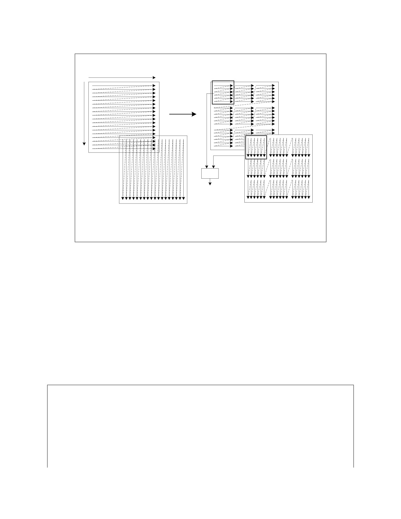
CODING FOR SIMD ARCHITECTURES
A(i, j) access pattern
A (i, j) access pattern
j
after blocking
Blocking
i
+
< cache size
B(i, j) access pattern
after blocking
OM15158
Figure 5-5. Loop Blocking Access Pattern
As one can see, all the redundant cache misses can be eliminated by applying this loop blocking tech-
nique. If MAX is huge, loop blocking can also help reduce the penalty from DTLB (data translation look-
aside buffer) misses. In addition to improving the cache/memory performance, this optimization tech-
nique also saves external bus bandwidth.
5.6
INSTRUCTION SELECTION
The following section gives some guidelines for choosing instructions to complete a task.
One barrier to SIMD computation can be the existence of data-dependent branches. Conditional moves
can be used to eliminate data-dependent branches. Conditional moves can be emulated in SIMD compu-
tation by using masked compares and logicals, as shown in Example 5-26. SSE4.1 provides packed blend
instruction that can vectorize data-dependent branches in a loop.
Example 5-26. Emulation of Conditional Moves
High-level code:
__declspec(align(16)) short A[MAX_ELEMENT], B[MAX_ELEMENT], C[MAX_ELEMENT], D[MAX_ELEMENT],
E[MAX_ELEMENT];
for (i=0; i<MAX_ELEMENT; i++) {
if (A[i] > B[i]) {
C[i] = D[i];
} else {
C[i] = E[i];
}
Ref#: 248966-047
5-26

CODING FOR SIMD ARCHITECTURES
Example 5-26. Emulation of Conditional Moves (Contd.)
}
MMX assembly code processes 4 short values per iteration:
xor
eax, eax
top_of_loop:
movq mm0, [A + eax]
pcmpgtw xmm0, [B + eax]; Create compare mask
movq mm1, [D + eax]
pand
mm1, mm0; Drop elements where A<B
pandn
mm0, [E + eax] ; Drop elements where A>B
por
mm0, mm1; Crete single word
movq
[C + eax], mm0
add
eax, 8
cmp
eax, MAX_ELEMENT*2
jle
top_of_loop
SSE4.1 assembly processes 8 short values per iteration:
xor
eax, eax
top_of_loop:
movdqq xmm0, [A + eax]
pcmpgtw xmm0, [B + eax]; Create compare mask
movdqa xmm1, [E + eax]
pblendv xmm1, [D + eax], xmm0;
movdqa [C + eax], xmm1;
add
eax, 16
cmp
eax, MAX_ELEMENT*2
jle
top_of_loop
If there are multiple consumers of an instance of a register, group the consumers together as closely as
possible. However, the consumers should not be scheduled near the producer.
5.7
TUNING THE FINAL APPLICATION
The best way to tune your application once it is functioning correctly is to use a profiler that measures the
application while it is running on a system. Intel VTune Amplifier XE can help you determine where to
make changes in your application to improve performance. Using Intel VTune Amplifier XE can help you
with various phases required for optimized performance. See Appendix A.3.1 for details. After every
effort to optimize, you should check the performance gains to see where you are making your major opti-
mization gains.
Ref#: 248966-047
5-27
4.
Updates to Chapter 20
Change bars and violet text show changes to Chapter 20 of the Intel® 64 and IA-32 Architectures Optimization
Resource Manual: Multicore and Hyper-Threading Technology.
------------------------------------------------------------------------------------------
Changes to this chapter:
• Section 20.5.3:
• Figures 20-3 and 20-4 were changed into tables due to illegibility. These tables are 20-3, 20-4, 20-5, and
20-6.
Intel® 64 and IA-32 Architectures Optimization Reference Manual Documentation Changes
13

INTEL® ADVANCED MATRIX EXTENSIONS (INTEL® AMX)
CHAPTER 20
INTEL® ADVANCED MATRIX EXTENSIONS (INTEL® AMX)
This chapter aims to help low-level DL programmers optimally code to the metal on Intel® Xeon® Proces-
sors based on Sapphire Rapids SP microarchitecture. It extends the public documentation on Optimizing
DL code with DL Boost instructions in Section 20.8.
It explains how to detect processor support in Intel® Advanced Matrix Extensions (Intel® AMX) Architec-
ture (Section 20.1). It provides an overview of Intel AMX architecture (Section 20.2) and presents Intel
AMX instruction throughput and latency (Section 20.3). It also discusses software optimization opportu-
nities for Intel AMX (Section 20.5 through Section 20.17), TileConfig/TileRelease and compiler ABI
(Section 20.18), Intel AMX state management and system software aspects (Section 20.19), and the use
of Intel AMX for higher precision GEMMs (Section 20.20).
Table 20-1. Intel® AMX-Related Links
Description
URL
Intel® AMX architecture definitions in the Intel®
64 and IA-32 Architecture Software
Developer’s Manual
Buildable and executable templates of code
examples for this chapter.
Open VINO™ Optimization Guide
tion_guide_dldt_optimization_guide.html
oneDNN GitHub
oneDNN documentation
Intel® Optimization TensorFlow Installation
Guide
cles/guide/optimization-for-tensorflow-installation-guide.html
PyTorch Landing Page
PyTorch GitHub
Intel® Neural Compressor (INC) GitHub
Tips for measuring the performance of matrix
nical/a-simple-example-to-measure-the-performance-of-an-intel-mkl-
multiplication using Intel® MKL
function.html
Intel® AMX ABI
GitHub Repository
Using dynamically enabled XSTATE features in
Linux user space applications
Ref#: 248966-048
20-1

INTEL® ADVANCED MATRIX EXTENSIONS (INTEL® AMX)
Table 20-1. Intel® AMX-Related Links
Description
URL
winbase-getenabledxstatefeatures
winbase-enableprocessoptionalxstatefeatures
Using dynamically enabled XSTATE features in
Windows user space applications
winbase-getthreadenabledxstatefeaturesv
threadsapi/nf-processthreadsapi-updateprocthreadattribute
20.1
DETECTING INTEL® AMX SUPPORT
Use the CPUID instruction described in Chapter 3.3 of the Intel® 64 and IA-32 Architecture Software
Developer’s Manual to find out whether the processor you are executing on supports Intel AMX at the
hardware level.
Specifically, when issuing the CPUID instruction with EAX register set to 7 and ECX register set to 0, the
instruction returns in the EDX register an indication on Intel AMX support of bits 22, 24, 25. They are all
set to 0 if Intel AMX is not supported and all set to 1 if it is supported by the processor.
Next step is check whether the OS has enabled Intel AMX state. For that you first need to issue the CPUID
instruction again to check whether the OS supports the XGETBV instruction, then use it to check whether
the OS has enabled the Intel AMX state save/restore.
When issuing the CPUID instruction with EAX register set to 1, the instruction returns an indication of
XGETBV support in bit 26 of the ECX register. If bit 26 is set, when issuing the XGETBV instruction with
ECX register set to 0, the instruction returns an indication on OS support in saving and restoring Intel
AMX state in bits 17 and 18 of the EAX register. Both bits should be set in order to use the Intel AMX
instructions. For additional CPUID information about Intel AMX, see Chapter 3.3 of the Intel® 64 and IA-
32 Architecture Software Developer’s Manual
Operating systems may require calling an OS API to allocate Intel AMX state. Visit LinuxAPI and Windows
APIs for more detailed information. Please see Section 20.19 for more information about Intel AMX state
management.
20.2
INTEL® AMX MICROARCHITECTURE OVERVIEW
General Intel AMX microarchitecture overview is available in Chapter 18 of Volume 1 of the Intel® 64 and
IA-32 Architectures Software Developer’s Manual.
20.2.1 INTEL® AMX FREQUENCIES
Discussion on the connection between max frequency, frequency license, and Instruction Set Architec-
ture covering Intel AVX technologies up to Intel® AVX-512 Instruction Set, is available in Section 2.5.3.
Intel AMX adds yet another license level whose max frequency is usually lower than that of the Intel AVX-
512 license.
When the Intel AMX unit utilization is lower than 15%, the processor may exceed the nominal max
frequency associated with Intel AMX license.
Ref#: 248966-048
20-2

INTEL® ADVANCED MATRIX EXTENSIONS (INTEL® AMX)
20.3
INTEL® AMX INSTRUCTIONS THROUGHPUT AND LATENCY
Several Intel AMX instructions are available. Two instructions (TileLoad*) load data from the memory
hierarchy into the tile registers and one instruction (TileStore) stores the contents of a tile register into
the DCU (Data Cache Unit-first level cache). Other instructions (TDP*) execute the matrix multiplication,
operating on two input tile registers and writing the result into a third tile register. Additionally, there are
some less-frequently used instructions. The following table provides the instruction throughput and
latency counted in cycles.
Table 20-2. Intel® AMX Instruction Throughput and Latency
Instruction
Throughput
Latency
LDTILECFG
Not Relevant
204
STTILECFG
Not Relevant
19
TILETRELEASE
Not Relevant
13
TDP/*
16
52
TILELOADD
8
45
TILELOADDT1
33
48
TILESTORED
16
TILEZERO
0
16
NOTE
Due to the high latency of the LDTILECFG instruction we recommend issuing a single pair
of LDTILECFG and TILERELEASE operations per Intel AMX-based DL layer implemen-
tation.
20.4
DATA STRUCTURE ALIGNMENT
GEMM and Convolution input/output data structures must be 64-byte aligned for optimal performance
but should not be aligned to 128-byte, 256-byte, etc. For more details, see Tip 6 in Tips for Measuring the
Performance of Matrix Multiplication Using Intel® MKL.
Ref#: 248966-048
20-3
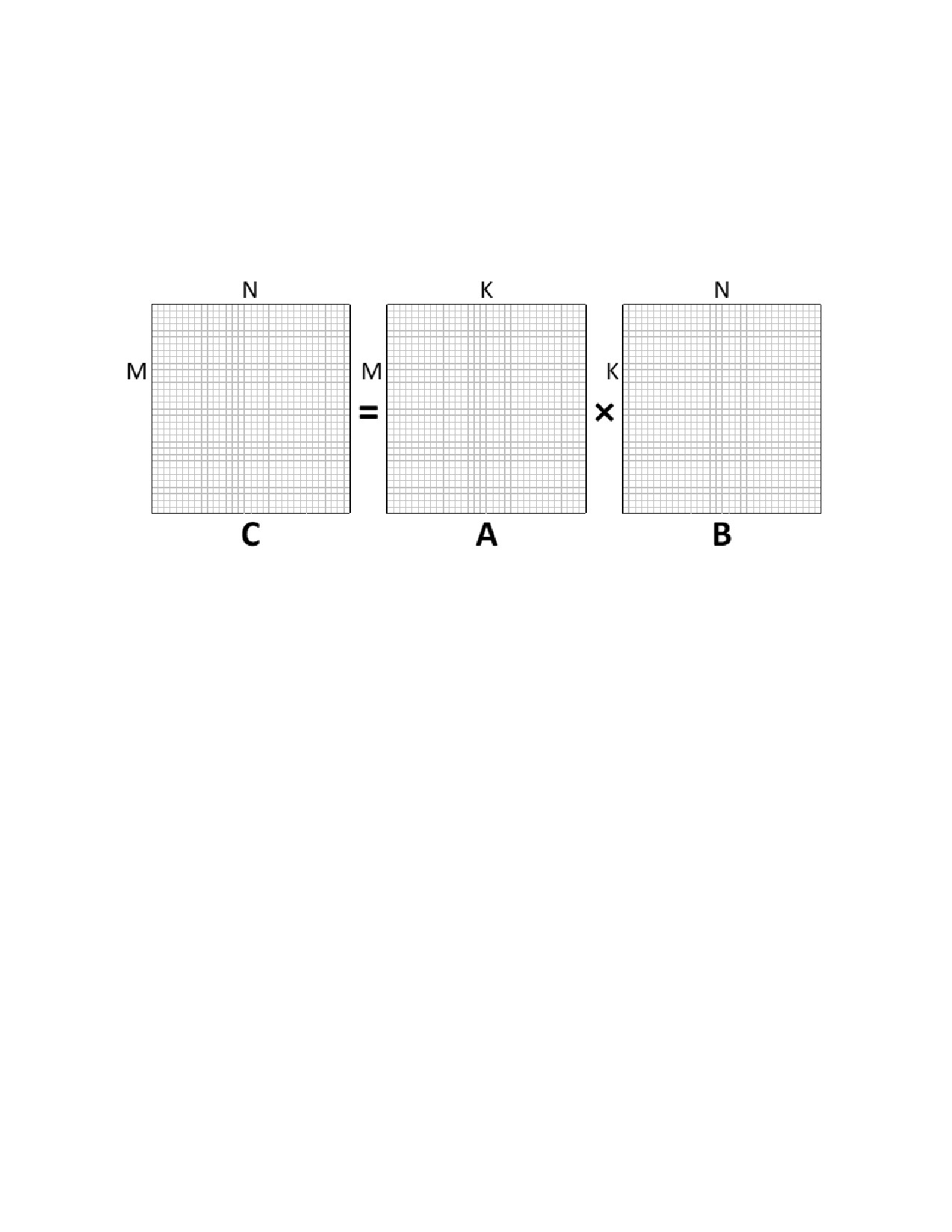
INTEL® ADVANCED MATRIX EXTENSIONS (INTEL® AMX)
20.5
GEMMS / CONVOLUTIONS
20.5.1 NOTATION
The following notation is used for the matrices (A, B, C) and the dimensions (M, K, N) in matrix multipli-
cation (GEMM).
Figure 20-1. Matrix Notation
20.5.2 TILES IN THE INTEL® AMX ARCHITECTURE
The Intel AMX instruction set operates on tiles: large two-dimensional registers with configurable dimen-
sions. The configuration is dependent on the type of tile.
• A-tiles can have between 1-16 rows and 1-MAX_TILE_K columns.
• B-tiles can have between 1-MAX_TILE_K rows and 1-16 columns.
• C-tiles can have between 1-16 rows and 1-16 columns.
MAX_TILE_K=64/sizeof(type_t), and type_t is the type of the data being operated on. Therefore,
MAX_TILE_K=64 for (u)int8 data, and MAX_TILE_K=32 for bfloat16 data. The dimensions here are
mathematical/logical. For mapping to tile register configuration parameters, see the Intel® Architecture
Instruction Set Extensions Programming Reference.
The type of data residing in the tiles also varies depending on the type of tile.
A tiles and B tiles contain data of type_t, which can be (u)int8 or bfloat16.
• C tiles contain data of type res_type_t:
• int32 if type_t=(u)int8
• float if type_t=bfloat16
Thus, a maximum-sized tile multiplication operation for (u)int8 data type looks this way:
Ref#: 248966-048
20-4
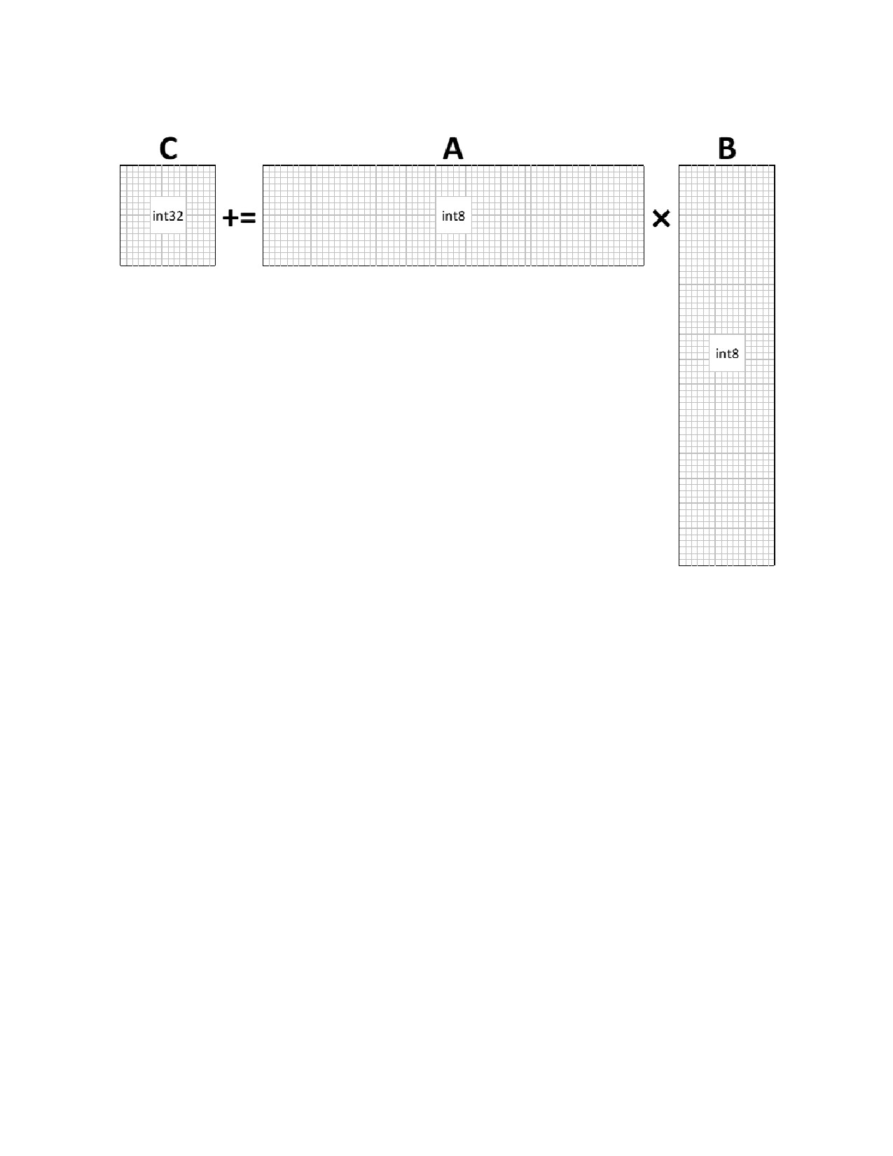
INTEL® ADVANCED MATRIX EXTENSIONS (INTEL® AMX)
Figure 20-2. Intel® AMX Multiplication with Max-sized int8 Tiles
TileLoad and TileStore Instructions
The tiles are loaded from memory with the TileLoad instruction and stored to memory with a TileStore
instruction. The TileLoad/TileStore instructions receive the following parameters:
• The destination/source tile of the TileLoad/TileStore.
• The source/destination location in memory for the TileLoad/TileStore.
• The stride (bytes) in memory between subsequent rows of the tile.
Ref#: 248966-048
20-5

INTEL® ADVANCED MATRIX EXTENSIONS (INTEL® AMX)
Lines 6—10 in Example 20-1 illustrate how a tile is loaded from memory.
Example 20-1. Pseudo-Code for the Tilezero, TileLoad, and TileStore Instructions
template<size_t rows, size_t bytes_cols> class tile {
public:
friend void tilezero(tile& t) {
memset(t.v, 0, sizeof(v));
}
friend void tileload(tile& t, void* src, size_t bytes_stride) {
for (size_t row = 0; row < rows; ++row)
for (size_t bcol = 0; bcol < bytes_cols; ++bcol)
t.v[row][bcol] = static_cast<int8_t*>(src)[row*bytes_stride + bcol];
}
friend void tilestore(tile& t, void* dst, size_t bytes_stride) {
for (size_t row = 0; row < rows; ++row)
for (size_t bcol = 0; bcol < bytes_cols; ++bcol)
static_cast<int8_t*>(dst)[row*bytes_stride + bcol] = t.v[row][bcol];
}
template <class TC, class TA, class TB>
friend void tdp(TC &tC, TA &tA, TB &tB);
private:
int8_t v[rows][bytes_cols];
};
// clang-format on
template <class TC, class TA, class TB> void tdp(TC &tC, TA &tA, TB &tB)
}
For the sake of readability, a tile template class abstraction is introduced. The number of rows in the tile
and the number of column bytes per row parametrizes the abstraction.
20.5.3 B MATRIX LAYOUT
Like the Intel® DL Boost use case, the B matrix must undergo a re-layout before it can be used within the
corresponding Intel AMX multiply instruction. The re-layout procedure is as follows:
Example 20-2. B Matrix Re-Layout Procedure
#define KPACK (4/sizeof(type_t))
// Vertical K packing into Dword
type_t B_mem_orig[K][N];
// Original B matrix
type_t B_mem[K/KPACK][N][KPACK];
// Re-laid B matrix
for (int k = 0; k < K; ++k)
for (int n = 0; n < N; ++n)
B_mem[k/KPACK][n][k%KPACK] = B_mem_orig[k][n];
The following tables illustrate the data re-layout process for a 64x16 int8 B matrix and a 32x16 bfloat16
B matrix (corresponding to the maximum-sized B-tile):
Ref#: 248966-048
20-6

INTEL® ADVANCED MATRIX EXTENSIONS (INTEL® AMX)
Table 20-3. Original Layout of 32x16 bfloat16 B-Matrix
0
1
2
3
4
5
6
7
8
9
10
11
12
13
14
15
16
17
18
19
20
21
22
23
24
25
26
27
28
29
30
31
32
33
34
35
36
37
38
39
40
41
42
43
44
45
46
47
48
49
50
51
52
53
54
55
56
57
58
59
60
61
62
63
64
65
66
67
68
69
70
71
72
73
74
75
76
77
78
79
80
81
82
83
84
85
86
87
88
89
90
91
92
93
95
95
96
97
98
99
100
101
102
103
104
105
106
107
108
109
110
111
112
113
114
115
116
117
118
119
120
121
122
123
124
125
126
127
128
129
130
131
132
133
134
135
136
137
138
139
140
141
142
143
144
145
146
147
148
149
150
151
152
153
154
155
156
157
158
159
160
161
162
163
164
165
166
167
168
169
170
171
172
173
174
175
176
177
178
179
180
181
182
183
184
185
186
187
188
189
190
191
192
193
194
195
196
197
198
199
200
201
202
203
204
205
206
207
208
209
210
211
212
213
214
215
216
217
218
219
220
221
222
223
224
225
226
227
228
229
230
231
232
233
234
235
236
237
238
239
240
241
242
243
244
245
246
247
248
249
250
251
252
253
254
255
256
257
258
259
260
261
262
263
264
265
266
267
268
269
270
271
272
273
274
275
276
277
278
279
280
281
282
283
284
285
286
287
288
289
290
291
292
293
294
295
296
297
298
299
300
301
302
303
304
305
306
307
308
309
310
311
312
313
314
315
316
317
318
319
320
321
322
323
324
325
326
327
328
329
330
331
332
333
334
335
336
337
338
339
340
341
342
343
344
345
346
347
348
349
350
351
352
353
354
355
356
357
358
359
360
361
362
363
364
365
366
367
368
369
370
371
372
373
374
375
376
377
378
379
380
381
382
383
384
385
386
387
388
389
390
391
392
393
394
395
396
397
398
399
400
401
402
403
404
405
406
407
408
409
410
411
412
413
414
415
416
417
418
419
420
421
422
423
424
425
426
427
428
429
430
431
432
433
434
435
436
437
438
439
440
441
442
443
444
445
446
447
448
449
450
451
452
453
454
455
456
457
458
459
460
461
462
463
464
465
466
467
468
469
470
471
472
473
474
475
476
477
478
479
480
481
482
483
484
485
486
487
488
489
490
491
492
493
494
495
496
497
498
499
500
501
502
503
504
505
506
507
508
509
510
511
Ref#: 248966-048
20-7

INTEL® ADVANCED MATRIX EXTENSIONS (INTEL® AMX)
Table 20-4. Re-Layout of 32x16 bfloat16 B-Matrix
Ref#: 248966-048
20-8

INTEL® ADVANCED MATRIX EXTENSIONS (INTEL® AMX)
Table 20-4.
(Contd.)Re-Layout of 32x16 bfloat16 B-Matrix
Table 20-5. Original Layout of 64 x 16 unt8 B-Matrix
4
5
6
7
8
9
10
11
12
13
14
15
20
21
22
23
24
25
26
27
28
29
30
31
36
37
38
39
40
41
42
43
44
45
46
47
52
53
54
55
56
57
58
59
60
61
62
63
68
69
70
71
72
73
74
75
76
77
78
79
84
85
86
87
88
89
90
91
92
93
94
95
100
101
102
103
104
105
106
107
108
109
110
111
116
117
118
119
120
121
122
123
124
125
126
127
132
133
134
135
136
137
138
139
140
141
142
143
148
149
150
151
152
153
154
155
156
157
158
159
164
165
166
167
168
169
170
171
172
173
174
175
180
181
182
183
184
185
186
187
188
189
190
191
196
197
198
199
200
201
202
203
204
205
206
207
212
213
214
215
216
217
218
219
220
221
222
223
228
229
230
231
232
233
234
235
236
237
238
239
244
245
246
247
248
249
250
251
252
253
254
255
260
261
262
263
264
265
266
267
268
269
270
271
276
277
278
279
280
281
282
283
284
285
286
287
Ref#: 248966-048
20-9

INTEL® ADVANCED MATRIX EXTENSIONS (INTEL® AMX)
Table 20-5. Original Layout of 64 x 16 unt8 B-Matrix
292
293
294
295
296
297
298
299
300
301
302
303
308
309
310
311
312
313
314
315
316
317
318
319
324
325
326
327
328
329
330
331
332
333
334
335
340
341
342
343
344
345
346
347
348
349
350
351
356
357
358
359
360
361
362
363
364
365
366
367
372
373
374
375
376
377
378
379
380
381
382
383
388
389
390
391
392
393
394
395
396
397
398
399
404
405
406
407
408
409
410
411
412
413
414
415
420
421
422
423
424
425
426
427
428
429
430
431
436
437
438
439
440
441
442
443
444
445
446
447
452
453
454
455
456
457
458
459
460
461
462
463
468
469
470
471
472
473
474
475
476
477
478
479
484
485
486
487
488
489
490
491
492
493
494
495
500
501
502
503
504
505
506
507
508
509
510
511
516
517
518
519
520
521
522
523
524
525
526
527
532
533
534
535
536
537
538
539
540
541
542
543
548
549
550
551
552
553
554
555
556
557
558
559
564
565
566
567
568
569
570
571
572
573
574
575
580
581
582
583
584
585
586
587
588
589
590
591
596
597
598
599
600
601
602
603
604
605
606
607
612
613
614
615
616
617
618
619
620
621
622
623
628
629
630
631
632
633
634
635
636
637
638
639
644
645
646
647
648
649
650
651
652
653
654
655
660
661
662
663
664
665
666
667
668
669
670
671
676
677
678
679
680
681
682
683
684
685
686
687
692
693
694
695
696
697
698
699
700
701
702
703
708
709
710
711
712
713
714
715
716
717
718
719
724
725
726
727
728
729
730
731
732
733
734
735
740
741
742
743
744
745
746
747
748
749
750
751
756
757
758
759
760
761
762
763
764
765
766
767
772
773
774
775
776
777
778
779
780
781
782
783
788
789
790
791
792
793
794
795
796
797
798
799
804
805
806
807
808
809
810
811
812
813
814
815
820
821
822
823
824
825
826
827
828
829
830
831
836
837
838
839
840
841
842
843
844
845
846
847
852
853
854
855
856
857
858
859
860
861
862
863
868
869
870
871
872
873
874
875
876
877
878
879
884
885
886
887
888
889
890
891
892
893
894
895
900
901
902
903
904
905
906
907
908
909
910
911
916
917
918
919
920
921
922
923
924
925
926
927
Ref#: 248966-048
20-10

INTEL® ADVANCED MATRIX EXTENSIONS (INTEL® AMX)
Table 20-5. Original Layout of 64 x 16 unt8 B-Matrix
932
933
934
935
936
937
938
939
940
941
942
943
948
949
950
951
952
953
954
955
956
957
958
959
964
965
966
967
968
969
970
971
972
973
974
975
980
981
982
983
984
985
986
987
988
989
990
991
996
997
998
999
1000
1001
1002
1003
1004
1005
1006
1007
1012
1013
1014
1015
1016
1017
1018
1019
1020
1021
1022
1023
Table 20-6. Re-Layout of 64 x 16 int8 B-Matrix
Ref#: 248966-048
20-11