Intel 64 and IA-32 Architectures. Software Developer’s Manual (Collection, 2023) - page 144
OPTIMIZATIONS FOR INTEL® AVX, INTEL® AVX2, AND INTEL® FMA
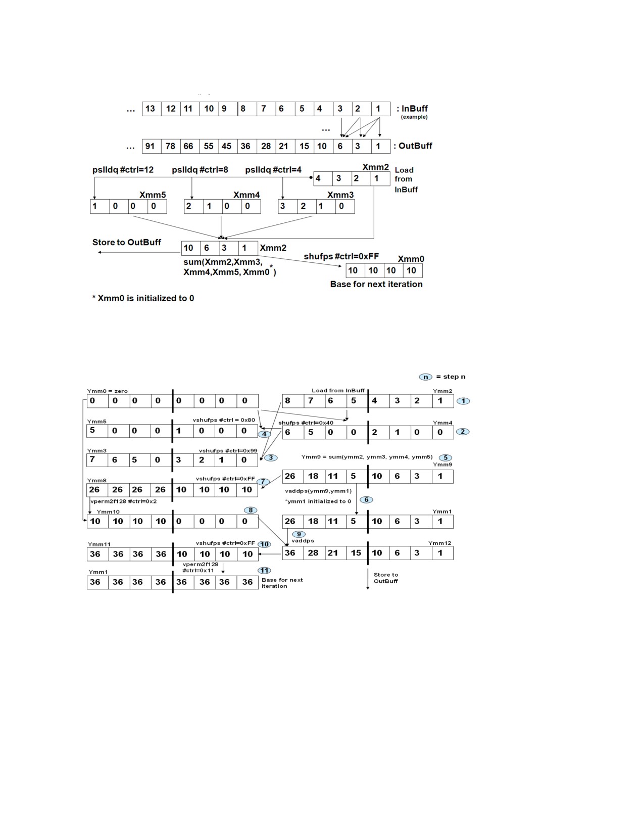
The figure below describes the Intel AVX implementation of the Array Sub Sums algorithm. The PSLLDQ
is an integer SIMD instruction which does not have an AVX equivalent. It is replaced by VSHUFPS.
15-44

OPTIMIZATIONS FOR INTEL® AVX, INTEL® AVX2, AND INTEL® FMA
Example 15-31. Array Sub Sums Algorithm
SSE code
AVX code
mov
rax, InBuff
mov
rax, InBuff
mov
rbx, OutBuff
mov
rbx, OutBuff
mov
rdx, len
mov
rdx, len
xor
rcx, rcx
xor
rcx, rcx
xorps
xmm0, xmm0
vxorps
ymm0, ymm0, ymm0
vxorps
ymm1, ymm1, ymm1
loop1:
loop1:
movaps
xmm2, [rax+4*rcx]
vmovaps
ymm2, [rax+4*rcx]
movaps
xmm3, xmm2
vshufps
ymm4, ymm0, ymm2, 0x40
movaps
xmm4, xmm2
vshufps
ymm3, ymm4, ymm2, 0x99
movaps
ymm5, ymm2
vshufps
ymm5, ymm0, ymm4, 0x80
pslldq
xmm3, 4
vaddps
ymm6, ymm2, ymm3
pslldq
xmm4, 8
vaddps
ymm7, ymm4, ymm5
pslldq
xmm5, 12
vaddps
ymm9, ymm6, ymm7
addps
xmm2, xmm3
vaddps
ymm1, ymm9, ymm1
addps
xmm4, xmm5
vshufps
ymm8, ymm9, ymm9, 0xff
addps
ymm2, xmm4
vperm2f128
ymm10, ymm8, ymm0, 0x2
addps
xmm2, xmm0
vaddps
ymm12, ymm1, ymm10
movaps
xmm0, ymm2
vshufps
ymm11, ymm12, ymm12, 0xff
shufps
xmm0, xmm2, 0xFF
vperm2f128
ymm1, ymm11, ymm11, 0x11
movaps
[rbx+4*rcx], xmm2
vmovaps
[rbx+4*rcx], ymm12
add
rcx, 4
add
rcx, 8
cmp
rcx, rdx
cmp
rcx, rdx
jl
loop1
jl
loop1
Example 15-31 shows SSE implementation of array sub sum and AVX implementation. The AVX code is
about 40% faster, though not on microarchitectures where there are more compute than shuffle ports.
15.14 HALF-PRECISION FLOATING-POINT CONVERSIONS
In applications that use floating-point and require only the dynamic range and precision offered by the
16-bit floating-point format, storing persistent floating-point data encoded in 16-bits has strong advan-
tages in memory footprint and bandwidth conservation. These situations are encountered in some
graphics and imaging workloads.
The encoding format of half-precision floating-point numbers can be found in Chapter 4, “Data Types” of
Intel® 64 and IA-32 Architectures Software Developer’s Manual, Volume 1.
Instructions to convert between packed, half-precision floating-point numbers and packed single-preci-
sion floating-point numbers is described in Chapter 14, “Programming with Intel® AVX, FMA, and Intel®
AVX2” of Intel® 64 and IA-32 Architectures Software Developer’s Manual, Volume 1 and in the reference pages of
Intel® 64 and IA-32 Architectures Software Developer’s Manual, Volume 2B.
To perform computations on half precision floating-point data, packed 16-bit FP data elements must be
converted to single precision format first, and the single-precision results converted back to half preci-
sion format, if necessary. These conversions of 8 data elements using 256-bit instructions are very fast
and handle the special cases of denormal numbers, infinity, zero and NaNs properly.
15-45

OPTIMIZATIONS FOR INTEL® AVX, INTEL® AVX2, AND INTEL® FMA
15.14.1 Packed Single-Precision to Half-Precision Conversion
To convert the data in single precision floating-point format to half precision format, without special hard-
ware support like VCVTPS2PH, a programmer needs to do the following:
• Correct exponent bias to permitted range for each data element.
• Shift and round the significand of each data element.
• Copy the sign bit to bit 15 of each element.
• Take care of numbers outside the half precision range.
• Pack each data element to a register of half size.
Example 15-32 compares two implementations of floating-point conversion from single precision to half
precision. The code on the left uses packed integer shift instructions that is limited to 128-bit SIMD
instruction set. The code on right is unrolled twice and uses the VCVTPS2PH instruction.
Example 15-32. Single-Precision to Half-Precision Conversion
AVX-128 code
VCVTPS2PH code
__asm {
__asm {
mov
rax, pIn
mov
rax, pIn
mov
rbx, pOut
mov
rbx, pOut
mov
rcx, bufferSize
mov
rcx, bufferSize
add
rcx, rax
add
rcx, rax
vmovdqu xmm0,SignMask16
loop:
vmovdqu xmm1,ExpBiasFixAndRound
vmovups
ymm0,[rax]
vmovdqu xmm4,SignMaskNot32
vmovups
ymm1,[rax+32]
vmovdqu xmm5,MaxConvertibleFloat
add
rax, 64
vmovdqu xmm6,MinFloat
vcvtps2ph
[rbx],ymm0, roundingCtrl
loop:
vcvtps2ph
[rbx+16],ymm1,roundingCtrl
vmovdqu
xmm2, [rax]
add
rbx, 32
vmovdqu
xmm3, [rax+16]
cmp
rax, rcx
vpaddd
xmm7, xmm2, xmm1
jl
loop
vpaddd
xmm9, xmm3, xmm1
vpand
xmm7, xmm7, xmm4
vpand
xmm9, xmm9, xmm4
add
rax, 32
vminps
xmm7, xmm7, xmm5
vminps
xmm9, xmm9, xmm5
vpcmpgtd
xmm8, xmm7, xmm6
vpcmpgtd
xmm10, xmm9, xmm6
vpand
xmm7, xmm8, xmm7
vpand
xmm9, xmm10, xmm9
vpackssdw
xmm2, xmm3, xmm2
vpsrad
xmm7, xmm7, 13
vpsrad
xmm8, xmm9, 13
vpand
xmm2, xmm2, xmm0
vpackssdw
xmm3, xmm7, xmm9
vpaddw
xmm3, xmm3, xmm2
vmovdqu
[rbx], xmm3
add
rbx, 16
cmp
rax, rcx
jl
loop
15-46

OPTIMIZATIONS FOR INTEL® AVX, INTEL® AVX2, AND INTEL® FMA
The code using VCVTPS2PH is approximately four times faster than the AVX-128 sequence. Although it is
possible to load 8 data elements at once with 256-bit AVX, most of the per-element conversion opera-
tions require packed integer instructions which do not have 256-bit extensions yet. Using VCVTPS2PH is
not only faster but also provides handling of special cases that do not encode to normal half-precision
floating-point values.
15.14.2 Packed Half-Precision to Single-Precision Conversion
Example 15-33 compares two implementations using AVX-128 code and with VCVTPH2PS.
Conversion from half precision to single precision floating-point format is easier to implement, yet using
VCVTPH2PS instruction performs about 2.5 times faster than the alternative AVX-128 code.
Example 15-33. Half-Precision to Single-Precision Conversion
AVX-128 code
VCVTPS2PH code
__asm {
__asm {
mov
rax, pIn
mov
rax, pIn
mov
rbx, pOut
mov
rbx, pOut
mov
rcx, bufferSize
mov
rcx, bufferSize
add
rcx, rax
add
rcx, rax
vmovdqu
xmm0,SignMask16
loop:
vmovdqu
xmm1,ExpBiasFix16
vcvtph2ps ymm0,[rax]
vmovdqu
xmm2,ExpMaskMarker
vcvtph2ps ymm1,[rax+16]
loop:
add
rax, 32
vmovdqu
xmm3, [rax]
vmovups
[rbx], ymm0
add
rax, 16
vmovups
[rbx+32], ymm1
vpandn
xmm4, xmm0, xmm3
add
rbx, 64
vpand
xmm5, xmm3, xmm0
cmp
rax, rcx
vpsrlw
xmm4, xmm4, 3
jl
loop
vpaddw
xmm6, xmm4, xmm1
vpcmpgtw
xmm7, xmm6, xmm2
vpand
xmm6, xmm6, xmm7
vpand
xmm8, xmm3, xmm7
vpor
xmm6, xmm6, xmm5
vpsllw
xmm8, xmm8, 13
vpunpcklwd
xmm3, xmm8, xmm6
vpunpckhwd xmm4, xmm8, xmm6
vmovdqu
[rbx], xmm3
vmovdqu
[rbx+16], xmm4
add
rbx, 32
cmp
rax, rcx
jl
loop
15.14.3 Locality Consideration for using Half-Precision FP to Conserve Bandwidth
Example 15-32 and Example 15-33 demonstrate the performance advantage of using FP16C instructions
when software needs to convert between half-precision and single-precision data. Half-precision FP
format is more compact, consumes less bandwidth than single-precision FP format, but sacrifices
dynamic range, precision, and incurs conversion overhead if arithmetic computation is required. Whether
it is profitable for software to use half-precision data will be highly dependent on locality considerations
of the workload.
15-47

OPTIMIZATIONS FOR INTEL® AVX, INTEL® AVX2, AND INTEL® FMA
This section uses an example based on the horizontal median filtering algorithm, “Median3”. The Median3
algorithm calculates the median of every three consecutive elements in a vector:
Y[i] = Median3( X[i], X[i+1], X[i+2])
Where: Y is the output vector, and X is the input vector.
Example 15-34 shows two implementations of the Median3 algorithm; one uses single-precision format
without conversion, the other uses half-precision format and requires conversion. Alternative 1 on the
left works with single precision format using 256-bit load/store operations, each of which loads/stores
eight 32-bit numbers. Alternative 2 uses 128-bit load/store operations to load/store eight 16-bit
numbers in half precision format and VCVTPH2PS/VCVTPS2PH instructions to convert it to/from single
precision floating-point format.
Example 15-34. Performance Comparison of Median3 using Half-Precision vs. Single-Precision
Single-Precision code w/o Conversion
Half-Precision code w/ Conversion
xor rbx, rbx
xor rbx, rbx
mov rcx, len
mov rcx, len
mov rdi, inPtr
mov rdi, inPtr
mov rsi, outPtr
mov rsi, outPtr
vmovaps ymm0, [rdi]
vcvtph2ps ymm0, [rdi]
loop:
loop:
add rdi, 32
add rdi,16
vmovaps ymm6, [rdi]
vcvtph2ps ymm6, [rdi]
vperm2f128 ymm1, ymm0, ymm6, 0x21
vperm2f128 ymm1, ymm0, ymm6, 0x21
vshufps ymm3, ymm0, ymm1, 0x4E
vshufps ymm3, ymm0, ymm1, 0x4E
vshufps ymm2, ymm0, ymm3, 0x99
vshufps ymm2, ymm0, ymm3, 0x99
vminps ymm5, ymm0, ymm2
vminps ymm5, ymm0, ymm2
vmaxps ymm0, ymm0, ymm2
vmaxps ymm0, ymm0, ymm2
vminps ymm4, ymm0, ymm3
vminps ymm4, ymm0, ymm3
vmaxps ymm7, ymm4, ymm5
vmaxps ymm7, ymm4, ymm5
vmovaps ymm0, ymm6
vmovaps ymm0, ymm6
vmovaps [rsi], ymm7
vcvtps2ph [rsi], ymm7, roundingCtrl
add rsi, 32
add rsi, 16
add rbx, 8
add rbx, 8
cmp rbx, rcx
cmp rbx, rcx
jl loop
jl loop
When the locality of the working set resides in memory, using half-precision format with processors
based on Ivy Bridge microarchitecture is about 30% faster than single-precision format, despite the
conversion overhead. When the locality resides in L3, using half-precision format is still ~15% faster.
When the locality resides in L1, using single-precision format is faster because the cache bandwidth of
the L1 data cache is much higher than the rest of the cache/memory hierarchy and the overhead of the
conversion becomes a performance consideration.
15.15 FUSED MULTIPLY-ADD (FMA) INSTRUCTIONS GUIDELINES
FMA instructions perform vectored operations of “a * b + c” on IEEE-754-2008 floating-point values,
where the multiplication operations “a * b” are performed with infinite precision, the final results of the
addition are rounded to produced the desired precision. Details of FMA rounding behavior and special
case handling can be found in section 2.3 of Intel® Architecture Instruction Set Extensions Programming
Reference.
15-48

OPTIMIZATIONS FOR INTEL® AVX, INTEL® AVX2, AND INTEL® FMA
FMA instruction can speed up and improve the accuracy of many FP calculations. Haswell microarchitec-
ture implements FMA instructions with execution units on port 0 and port 1 and 256-bit data paths. Dot
product, matrix multiplication and polynomial evaluations are expected to benefit from the use of FMA,
256-bit data path and the independent executions on two ports. The peak throughput of FMA from each
processor core are 16 single-precision and 8 double-precision results each cycle.
Algorithms designed to use FMA instruction should take into consideration that non-FMA sequence of
MULPD/PS and ADDPD/PS likely will produce slightly different results compared to using FMA. For numer-
ical computations involving a convergence criteria, the difference in the precision of intermediate results
must be factored into the numeric formalism to avoid surprise in completion time due to rounding issues.
User/Source Coding Rule 28. Factor in precision and rounding characteristics of FMA instructions
when replacing multiply/add operations executing non-FMA instructions. FMA improves performance
when an algorithm is execution-port throughput limited, like DGEMM.
There may be situations where using FMA might not deliver better performance. Consider the vectored
operation of “a * b + c * d” and data are ready at the same time:
In the three-instruction sequence of
VADDPS ( VMULPS (a,b) , VMULPS (c,b) );
VMULPS can be dispatched in the same cycle and execute in parallel, leaving the latency of VADDPS (3
cycle) exposed. With unrolling the exposure of VADDPS latency may be further amortized.
When using the two-instruction sequence of
VFMADD213PS ( c, d, VMULPS (a,b) );
The latency of FMA (5 cycle) is exposed for producing each vector result.
User/Source Coding Rule 29. Factor in result-dependency, latency of FP add vs. FMA instructions
when replacing FP add operations with FMA instructions.
15.15.1 Optimizing Throughput with FMA and Floating-Point Add/MUL
In the Skylake microarchitecture, there are two pipes of executions supporting FMA, vector FP Multiply,
and FP ADD instructions. All three categories of instructions have a latency of 4 cycles and can dispatch
to either port 0 or port 1 to execute every cycle.
The arrangement of identical latency and number of pipes allows software to increase the performance of
situations where floating-point calculations are limited by the floating-point add operations that follow FP
multiplies. Consider a situation of vector operation An = C1 + C2 * An-1:
Example 15-35. FP Mul/FP Add Versus FMA
FP Mul/FP Add Sequence
FMA Sequence
mov eax, NumOfIterations
mov eax, NumOfIterations
mov rbx, pA
mov rbx, pA
mov rcx, pC1
mov rcx, pC1
mov rdx, pC2
mov rdx, pC2
vmovups ymm0, ymmword ptr [rbx] // A
vmovups ymm0, ymmword ptr [rbx] // A
vmovups ymm1, ymmword ptr [rcx] // C1
vmovups ymm1, ymmword ptr [rcx] // C1
vmovups ymm2, ymmword ptr [rdx] // C2
vmovups ymm2, ymmword ptr [rdx] // C2
loop:
loop:
vmulps ymm4, ymm0 ,ymm2 // A * C2
vfmadd132ps ymm0, ymm1, ymm2 // C1 + A * C2
vaddps ymm0, ymm1, ymm4
dec eax
dec eax
jnz loop
jnz loop
vmovups ymmword ptr[rbx], ymm0 // store A
vmovups ymmword ptr[rbx], ymm0 // store A
15-49

OPTIMIZATIONS FOR INTEL® AVX, INTEL® AVX2, AND INTEL® FMA
Example 15-35. FP Mul/FP Add Versus FMA
FP Mul/FP Add Sequence
FMA Sequence
Cost per iteration: ~ fp add latency + fp add latency
Cost per iteration: ~ fma latency
The overall throughput of the code sequence on the LHS is limited by the combined latency of the FP MUL
and FP ADD instructions of specific microarchitecture. The overall throughput of the code sequence on
the RHS is limited by the throughput of the FMA instruction of the corresponding microarchitecture.
A common situation where the latency of the FP ADD operation dominates performance is the following
C code:
for ( int 1 = 0; i < arrLenght; i ++) result += arrToSum[i];
Example 15-35 shows two implementations with and without unrolling.
Example 15-36. Unrolling to Hide Dependent FP Add Latency
No Unroll
Unroll 8 times
mov eax, arrLength
mov eax, arrLength
mov rbx, arrToSum
mov rbx, arrToSum
vmovups ymm0, ymmword ptr [rbx]
vmovups ymm0, ymmword ptr [rbx]
sub eax, 8
vmovups ymm1, ymmword ptr 32[rbx]
loop:
vmovups ymm2, ymmword ptr 64[rbx]
add rbx, 32
vmovups ymm3, ymmword ptr 96[rbx]
vaddps ymm0, ymm0, ymmword ptr [rbx]
vmovups ymm4, ymmword ptr 128[rbx]
sub eax, 8
vmovups ymm5, ymmword ptr 160[rbx]
jnz loop
vmovups ymm6, ymmword ptr 192[rbx]
vmovups ymm7, ymmword ptr 224[rbx]
vextractf128 xmm1, ymm0, 1
sub eax, 64
vaddps xmm0, xmm0, xmm1
loop:
vpermilps xmm1, xmm0, 0xe
add rbx, 256
vaddps xmm0, xmm0, xmm1
vaddps ymm0, ymm0, ymmword ptr [rbx]
vpermilps xmm1, xmm0, 0x1
vaddps ymm1, ymm1, ymmword ptr 32[rbx]
vaddss xmm0, xmm0, xmm1
vaddps ymm2, ymm2, ymmword ptr 64[rbx]
vaddps ymm3, ymm3, ymmword ptr 96[rbx]
vaddps ymm4, ymm4, ymmword ptr 128[rbx]
vaddps ymm5, ymm5, ymmword ptr 160[rbx]
vaddps ymm6, ymm6, ymmword ptr 192[rbx]
vaddps ymm7, ymm7, ymmword ptr 224[rbx]
sub eax, 64
jnz loop
vaddps ymm0, ymm0, ymm1
vaddps ymm2, ymm2, ymm3
vaddps ymm4, ymm4, ymm5
vaddps ymm6, ymm6, ymm7
vaddps ymm0, ymm0, ymm2
vaddps ymm4, ymm4, ymm6
vaddps ymm0, ymm0, ymm4
15-50

OPTIMIZATIONS FOR INTEL® AVX, INTEL® AVX2, AND INTEL® FMA
Example 15-36. Unrolling to Hide Dependent FP Add Latency (Contd.)
No Unroll
Unroll 8 times
movss result, xmm0
vextractf128 xmm1, ymm0, 1
vaddps xmm0, xmm0, xmm1
vpermilps xmm1, xmm0, 0xe
vaddps xmm0, xmm0, xmm1
vpermilps xmm1, xmm0, 0x1
vaddss xmm0, xmm0, xmm1
movss result, xmm0
Without unrolling (LHS of Example 15-35), the cost of summing every 8 array elements is about propor-
tional to the latency of the FP ADD instruction, assuming the working set fit in L1. To use unrolling effec-
tively, the number of unrolled operations should be at least “latency of the critical operation” * “number
of pipes”. The performance gain of optimized unrolling versus no unrolling, for a given microarchitecture,
can approach “number of pipes” * “Latency of FP ADD”.
User/Source Coding Rule 30. Consider using unrolling technique for loops containing back-to-back
dependent FMA, FP Add or Vector MUL operations, The unrolling factor can be chosen by considering
the latency of the critical instruction of the dependency chain and the number of pipes available to
execute that instruction.
15.15.2 Optimizing Throughput with Vector Shifts
In the Skylake microarchitecture, many common vector shift instructions can dispatch into either port 0
or port 1, compared to only one port in prior generations, see Table 2-12 and Table E-2.
A common situation where the latency of the FP ADD operation dominates performance is the following
C code, where a, b, and c are integer arrays:
for ( int 1 = 0; i < len; i ++) c[i] += 4* a[i] + b[i]/2;
Example 15-35 shows two implementations with and without unrolling.
Example 15-37. FP Mul/FP Add Versus FMA
FP Mul/FP Add Sequence
FMA Sequence
mov eax, NumOfIterations
mov eax, NumOfIterations
mov rbx, pA
mov rbx, pA
mov rcx, pC1
mov rcx, pC1
mov rdx, pC2
mov rdx, pC2
vmovups ymm0, ymmword ptr [rbx] // A
vmovups ymm0, ymmword ptr [rbx] // A
vmovups ymm1, ymmword ptr [rcx] // C1
vmovups ymm1, ymmword ptr [rcx] // C1
vmovups ymm2, ymmword ptr [rdx] // C2
vmovups ymm2, ymmword ptr [rdx] // C2
loop:
loop:
vmulps ymm4, ymm0 ,ymm2 // A * C2
vfmadd132ps ymm0, ymm1, ymm2 // C1 + A * C2
vaddps ymm0, ymm1, ymm4
dec eax
dec eax
jnz loop
jnz loop
vmovups ymmword ptr[rbx], ymm0 // store An
vmovups ymmword ptr[rbx], ymm0 // store An
Cost per iteration: ~ fp add latency + fp add latency
Cost per iteration: ~ fma latency
15-51
OPTIMIZATIONS FOR INTEL® AVX, INTEL® AVX2, AND INTEL® FMA
15.16 AVX2 OPTIMIZATION GUIDELINES
AVX2 instructions promotes the great majority of 128-bit SIMD integer instructions to operate on 256-bit
YMM registers. AVX2 also adds a rich mix of broadcast/permute/variable-shift instructions to accelerate
numerical computations. The 256-bit AVX2 instructions are supported by Haswell microarchitecture,
which implements 256-bit data path with low latency and high throughput.
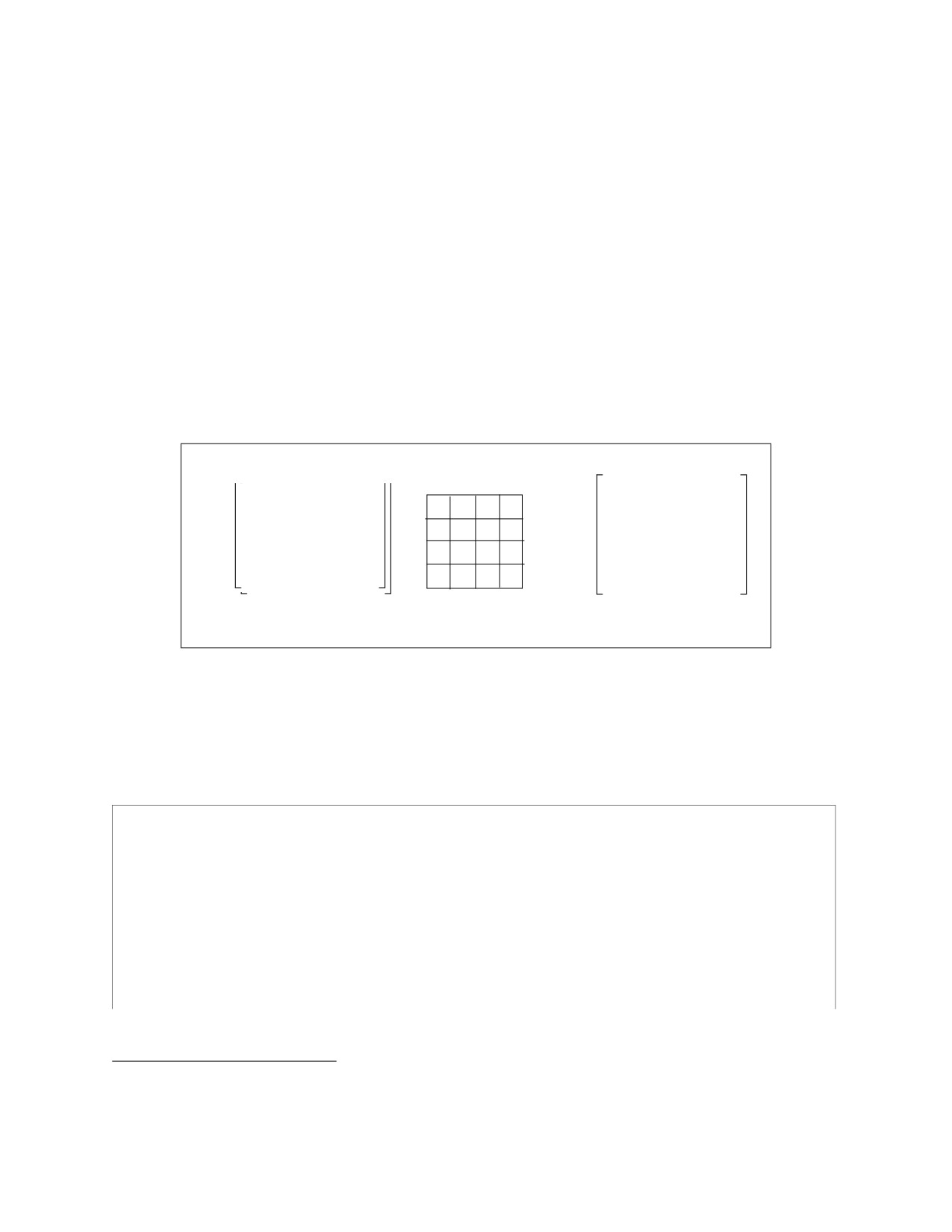
Consider an intra-coding 4x4 block image transformation1 shown in Figure 15-3.
A 128-bit SIMD implementation can perform this transformation by the following technique:
• Convert 8-bit pixels into 16-bit word elements and fetch two 4x4 image block as 4 row vectors.
• The matrix operation 1/128 * (B x R) can be evaluated with row vectors of the image block and
column vectors of the right-hand-side coefficient matrix using a sequence of SIMD instructions of
PMADDWD, packed shift and blend instructions.
• The two 4x4 word-granular, intermediate result can be re-arranged into column vectors.
• The left-hand-side coefficient matrix in row vectors and the column vectors of the intermediate block
can be calculated (using PMADDWD, shift, blend) and written out.
29
55
74
84
64
64
64
64
-------
74
74
0
-74
X
84
35
-35 -84
X
-------
128
84 -29 -74
55
128
64 -64 -64
64
55 -84
74
-29
35 -84
84
-35
L
B
R
Figure 15-3.
4x4 Image Block Transformation
The same technique can be implemented using AVX2 instructions in a straightforward manner. The AVX2
sequence is illustrated in Example 15-38 and Example 15-39.
Example 15-38. Macros for Separable KLT Intra-block Transformation Using AVX2
// b0: input row vector from 4 consecutive 4x4 image block of word pixels
// rmc0-3: columnar vector coefficient of the RHS matrix, repeated 4X for 256-bit
// min32km1: saturation constant vector to cap intermediate pixel to less than or equal to 32767
// w0: output row vector of garbled intermediate matrix, elements within each block are garbled
// e.g Low 128-bit of row 0 in descending order: y07, y05, y06, y04, y03, y01, y02, y00
#define __MyM_KIP_PxRMC_ROW_4x4Wx4(b0, w0, rmc0_256,
rmc1_256, rmc2_256, rmc3_256, min32km1)\
1. C. Yeo, Y. H. Tan, Z. Li and S. Rahardja, “Mode-Dependent Fast Separable KLT for Block-based Intra
Coding,” JCTVC-B024, Geneva, Switzerland, Jul 2010
15-52

OPTIMIZATIONS FOR INTEL® AVX, INTEL® AVX2, AND INTEL® FMA
Example 15-38. Macros for Separable KLT Intra-block Transformation Using AVX2 (Contd.)
{__m256i tt0, tt1, tt2, tt3, tttmp;\
tt0 = _mm256_madd_epi16(b0, (rmc0_256));\
tt1 = _mm256_madd_epi16(b0, rmc1_256);\
tt1 = _mm256_hadd_epi32(tt0, tt1);\
tttmp = _mm256_srai_epi32( tt1, 31);\
tttmp = _mm256_srli_epi32( tttmp, 25);\
tt1 = _mm256_add_epi32( tt1, tttmp);\
tt1 = _mm256_min_epi32(_mm256_srai_epi32( tt1, 7), min32km1);\
tt1 = _mm256_shuffle_epi32(tt1, 0xd8); \
tt2 = _mm256_madd_epi16(b0, rmc2_256);\
tt3 = _mm256_madd_epi16(b0, rmc3_256);\
tt3 = _mm256_hadd_epi32(tt2, tt3);\
tttmp = _mm256_srai_epi32( tt3, 31);\
tttmp = _mm256_srli_epi32( tttmp, 25);\
tt3 = _mm256_add_epi32( tt3, tttmp);\
tt3 = _mm256_min_epi32( _mm256_srai_epi32(tt3, 7), min32km1);\
tt3 = _mm256_shuffle_epi32(tt3, 0xd8);\
w0 = _mm256_blend_epi16(tt1, _mm256_slli_si256( tt3, 2), 0xaa);\
}
// t0-t3: 256-bit input vectors of un-garbled intermediate matrix 1/128 * (B x R)
// lmr_256: 256-bit vector of one row of LHS coefficient, repeated 4X
// min32km1: saturation constant vector to cap final pixel to less than or equal to 32767
// w0; Output row vector of final result in un-garbled order
#define __MyM_KIP_LMRxP_ROW_4x4Wx4(w0, t0, t1, t2, t3, lmr_256, min32km1)\
{__m256i tb0, tb1, tb2, tb3, tbtmp;
tb0 = _mm256_madd_epi16( lmr_256, t0);\
tb1 = _mm256_madd_epi16( lmr_256, t1);\
tb1 = _mm256_hadd_epi32(tb0, tb1);\
tbtmp = _mm256_srai_epi32( tb1, 31);\
tbtmp = _mm256_srli_epi32( tbtmp, 25);\
tb1 = _mm256_add_epi32( tb1, tbtmp);\
tb1 = _mm256_min_epi32( _mm256_srai_epi32( tb1, 7), min32km1);\
tb1 = _mm256_shuffle_epi32(tb1, 0xd8);\
tb2 = _mm256_madd_epi16( lmr_256, t2);\
tb3 = _mm256_madd_epi16( lmr_256, t3);\
tb3 = _mm256_hadd_epi32(tb2, tb3);\
tbtmp = _mm256_srai_epi32( tb3, 31);\
tbtmp = _mm256_srli_epi32( tbtmp, 25);\
tb3 = _mm256_add_epi32( tb3, tbtmp);\
tb3 = _mm256_min_epi32( _mm256_srai_epi32( tb3, 7), min32km1);\
tb3 = _mm256_shuffle_epi32(tb3, 0xd8); \
tb3 = _mm256_slli_si256( tb3, 2);\
tb3 = _mm256_blend_epi16(tb1, tb3, 0xaa);\
15-53

OPTIMIZATIONS FOR INTEL® AVX, INTEL® AVX2, AND INTEL® FMA
Example 15-38. Macros for Separable KLT Intra-block Transformation Using AVX2 (Contd.)
w0 = _mm256_shuffle_epi8(tb3, _mm256_setr_epi32( 0x5040100, 0x7060302, 0xd0c0908, 0xf0e0b0a,
0x5040100, 0x7060302, 0xd0c0908, 0xf0e0b0a));\
}
In Example 15-39, matrix multiplication of 1/128 * (B xR) is evaluated first in a 4-wide manner by
fetching from 4 consecutive 4x4 image block of word pixels. The first macro shown in Example 15-38
produces an output vector where each intermediate row result is in an garbled sequence between the two
middle elements of each 4x4 block. In Example 15-39, undoing the garbled elements and transposing
the intermediate row vector into column vectors are implemented using blend primitives instead of
shuffle/unpack primitives.
In Haswell microarchitecture, shuffle/pack/unpack primitives rely on the shuffle execution unit
dispatched to port 5. In some situations of heavy SIMD sequences, port 5 pressure may become a deter-
mining factor in performance.
If 128-bit SIMD code faces port 5 pressure when running on Haswell microarchitecture, porting 128-bit
code to use 256-bit AVX2 can improve performance and alleviate port 5 pressure.
Example 15-39. Separable KLT Intra-block Transformation Using AVX2
short __declspec(align(16))cst_rmc0[8] = {64, 84, 64, 35, 64, 84, 64, 35};
short __declspec(align(16))cst_rmc1[8] = {64, 35, -64, -84, 64, 35, -64, -84};
short __declspec(align(16))cst_rmc2[8] = {64, -35, -64, 84, 64, -35, -64, 84};
short __declspec(align(16))cst_rmc3[8] = {64, -84, 64, -35, 64, -84, 64, -35};
short __declspec(align(16))cst_lmr0[8] = {29, 55, 74, 84, 29, 55, 74, 84};
short __declspec(align(16))cst_lmr1[8] = {74, 74, 0, -74, 74, 74, 0, -74};
short __declspec(align(16))cst_lmr2[8] = {84, -29, -74, 55, 84, -29, -74, 55};
short __declspec(align(16)) cst_lmr3[8] = {55, -84, 74, -29, 55, -84, 74, -29};
void Klt_256_d(short * Input, short * Output, int iWidth, int iHeight)
{int iX, iY;
__m256i rmc0 = _mm256_broadcastsi128_si256( _mm_loadu_si128((__m128i *) &cst_rmc0[0]));
__m256i rmc1 = _mm256_broadcastsi128_si256( _mm_loadu_si128((__m128i *)&cst_rmc1[0]));
__m256i rmc2 = _mm256_broadcastsi128_si256( _mm_loadu_si128((__m128i *)&cst_rmc2[0]));
__m256i rmc3 = _mm256_broadcastsi128_si256( _mm_loadu_si128((__m128i *)&cst_rmc3[0]));
__m256i lmr0 = _mm256_broadcastsi128_si256( _mm_loadu_si128((__m128i *)&cst_lmr0[0]));
__m256i lmr1 = _mm256_broadcastsi128_si256( _mm_loadu_si128((__m128i *)&cst_lmr1[0]));
__m256i lmr2 = _mm256_broadcastsi128_si256( _mm_loadu_si128((__m128i *)&cst_lmr2[0]));
__m256i lmr3 = _mm256_broadcastsi128_si256( _mm_loadu_si128((__m128i *)&cst_lmr3[0]));
__m256i min32km1 = _mm256_broadcastd_epi32(_mm_cvtsi32_si128( _mm_setr_epi32( 0x7fff7fff, 0x7fff7fff,
0x7fff7fff, 0x7fff7fff));
__m256i b0, b1, b2, b3, t0, t1, t2, t3;
__m256i w0, w1, w2, w3;
short* pImage = Input;
short* pOutImage = Output;
int hgt = iHeight, wid= iWidth;
(continue)
15-54

OPTIMIZATIONS FOR INTEL® AVX, INTEL® AVX2, AND INTEL® FMA
Example 15-39. Separable KLT Intra-block Transformation Using AVX2 (Contd.)
// We implement 1/128 * (Mat_L x (1/128 * (Mat_B x Mat_R))) from the inner most parenthesis
for( iY = 0; iY < hgt; iY+=4) {
for( iX = 0; iX < wid; iX+=16) {
//load row 0 of 4 consecutive 4x4 matrix of word pixels
b0 = _mm256_loadu_si256( (__m256i *) (pImage + iY*wid+ iX)) ;
// multiply row 0 with columnar vectors of the RHS matrix coefficients
__MyM_KIP_PxRMC_ROW_4x4Wx4(b0, w0, rmc0, rmc1, rmc2, rmc3, min32km1);
// low 128-bit of garbled row 0, from hi->lo: y07, y05, y06, y04, y03, y01, y02, y00
b1 = _mm256_loadu_si256( (__m256i *) (pImage + (iY+1)*wid+ iX) );
__MyM_KIP_PxRMC_ROW_4x4Wx4(b1, w1, rmc0, rmc1, rmc2, rmc3, min32km1);
// hi->lo y17, y15, y16, y14, y13, y11, y12, y10
b2 = _mm256_loadu_si256( (__m256i *) (pImage + (iY+2)*wid+ iX) );
__MyM_KIP_PxRMC_ROW_4x4Wx4(b2, w2, rmc0, rmc1, rmc2, rmc3, min32km1);
b3 = _mm256_loadu_si256( (__m256i *) (pImage + (iY+3)*wid+ iX) );
__MyM_KIP_PxRMC_ROW_4x4Wx4(b3, w3, rmc0, rmc1, rmc2, rmc3, min32km1);
// unscramble garbled middle 2 elements of each 4x4 block, then
// transpose into columnar vectors: t0 has 4 consecutive column 0 or 4 4x4 intermediate
t0 = _mm256_blend_epi16( w0, _mm256_slli_epi64(w1, 16), 0x22);
t0 = _mm256_blend_epi16( t0, _mm256_slli_epi64(w2, 32), 0x44);
t0 = _mm256_blend_epi16( t0, _mm256_slli_epi64(w3, 48), 0x88);
t1 = _mm256_blend_epi16( _mm256_srli_epi64(w0, 32), _mm256_srli_epi64(w1, 16), 0x22);
t1 = _mm256_blend_epi16( t1, w2, 0x44);
t1 = _mm256_blend_epi16( t1, _mm256_slli_epi64(w3, 16), 0x88); // column 1
t2 = _mm256_blend_epi16( _mm256_srli_epi64(w0, 16), w1, 0x22);
t2 = _mm256_blend_epi16( t2, _mm256_slli_epi64(w2, 16), 0x44);
t2 = _mm256_blend_epi16( t2, _mm256_slli_epi64(w3, 32), 0x88); // column 2
t3 = _mm256_blend_epi16( _mm256_srli_epi64(w0, 48), _mm256_srli_epi64(w1, 32), 0x22);
t3 = _mm256_blend_epi16( t3, _mm256_srli_epi64(w2, 16), 0x44);
t3 = _mm256_blend_epi16( t3, w3, 0x88);// column 3
// multiply row 0 of the LHS coefficient with 4 columnar vectors of intermediate blocks
// final output row are arranged in normal order
__MyM_KIP_LMRxP_ROW_4x4Wx4(w0, t0, t1, t2, t3, lmr0, min32km1);
_mm256_store_si256( (__m256i *) (pOutImage+iY*wid+ iX), w0) ;
__MyM_KIP_LMRxP_ROW_4x4Wx4(w1, t0, t1, t2, t3, lmr1, min32km1);
_mm256_store_si256( (__m256i *) (pOutImage+(iY+1)*wid+ iX), w1) ;
__MyM_KIP_LMRxP_ROW_4x4Wx4(w2, t0, t1, t2, t3, lmr2, min32km1);
_mm256_store_si256( (__m256i *) (pOutImage+(iY+2)*wid+ iX), w2) ;
15-55

OPTIMIZATIONS FOR INTEL® AVX, INTEL® AVX2, AND INTEL® FMA
Example 15-39. Separable KLT Intra-block Transformation Using AVX2 (Contd.)
__MyM_KIP_LMRxP_ROW_4x4Wx4(w3, t0, t1, t2, t3, lmr3, min32km1);
_mm256_store_si256( (__m256i *) (pOutImage+(iY+3)*wid+ iX), w3) ;
}
}
}
Although 128-bit SIMD implementation is not shown here, it can be easily derived.
When running 128-bit SIMD code of this KLT intra-coding transformation on Sandy Bridge microarchitec-
ture, the port 5 pressure are less because there are two shuffle units, and the effective throughput for
each 4x4 image block transformation is around 50 cycles. Its speed-up relative to optimized scalar imple-
mentation is about 2.5X.
When the 128-bit SIMD code runs on Haswell microarchitecture, micro-ops issued to port 5 account for
slightly less than 50% of all micro-ops, compared to about one third on prior microarchitecture, resulting
in about 25% performance regression. On the other hand, AVX2 implementation can deliver effective
throughput in less than 35 cycle per 4x4 block.
15.16.1 Multi-Buffering and AVX2
There are many compute-intensive algorithms (e.g. hashing, encryption, etc.) which operate on a
stream of data buffers. Very often, the data stream may be partitioned and treated as multiple indepen-
dent buffer streams to leverage SIMD instruction sets.
Detailed treatment of hashing several buffers in parallel can be found at
http://eprint.iacr.org/2012/476.pdf.
With AVX2 providing a full compliment of 256-bit SIMD instructions with rich functionality at multiple
width granularities for logical and arithmetic operations. Algorithms that had leveraged XMM registers
and prior generations of SSE instruction sets can extend those multi-buffering algorithms to use AVX2 on
YMM and deliver even higher throughput. Optimized 256-bit AVX2 implementation may deliver up to
1.9X throughput when compared to 128-bit versions.
The image block transformation example discussed in Section 15.16 can be construed also as a multi-
buffering implementation of 4x4 blocks. When the performance baseline is switched from a two-shuffle-
port microarchitecture (Sandy Bridge) to single-shuffle-port microarchitecture, the 256-bit wide AVX2
provides a speed up of 1.9X relative to 128-bit SIMD implementation.
Greater details on multi-buffering can be found in the white paper at:
multi-buffer-paper.pdf.
15.16.2 Modular Multiplication and AVX2
Modular multiplication of very large integers are often used to implement efficient modular exponentia-
tion operations which are critical in public key cryptography, such as RSA 2048. Library implementation
of modular multiplication is often done with MUL/ADC chain sequences. Typically, a MUL instruction can
produce a 128-bit intermediate integer output, and add-carry chains must be used at 64-bit intermediate
data granularity.
In AVX2, VPMULUDQ/VPADDQ/VPSRLQ/VPSLLQ/VPBROADCASTQ/VPERMQ allow vectorized approach to
implement efficient modular multiplication/exponentiation for key lengths corresponding to RSA1024
and RSA2048. For details of modular exponentiation/multiplication and AVX2 implementation in
OpenSSL, see http://rd.springer.com/chapter/10.1007%2F978-3-642-31662-3_9?LI=true.
15-56
OPTIMIZATIONS FOR INTEL® AVX, INTEL® AVX2, AND INTEL® FMA
The basic heuristic starts with reformulating the large integer input operands in 512/1024 bit exponenti-
ation in redundant representations. For example, a 1024-bit integer can be represented using base 2^29
and 36 “digits”, where each “digit” is less than 2^29. A digit in such redundant representation can be
placed in a dword slot of a vector register. Such redundant representation of large integer simplifies the
requirement to perform carry-add chains across the hardware granularity of the intermediate results of
unsigned integer multiplications.
Each VPMULUDQ in AVX2 using the digits from a redundant representation can produce 4 separate 64-
bit intermediate result with sufficient headroom (e.g. 5 most significant bits are 0 excluding sign bit).
Then, VPADDQ is sufficient to implement add-carry chain requirement without needing SIMD versions of
equivalent of ADC-like instructions. More details are available in the reference cited in paragraph above,
including the cost factor of conversion to redundant representation and effective speedup accounting for
parallel output bandwidth of VPMULUDQ/VPADDQ chain.
15.16.3 Data Movement Considerations
Haswell microarchitecture can support up to two 256-bit loads and one 256-bit store micro-ops
dispatched each cycle. Most existing binaries with heavy data-movement operation can benefit from this
enhancement and the higher bandwidths of the L1 data cache and L2 without re-compilation, if the
binary is already optimized for the prior generation microarchitecture. For example, 256-bit SAXPY
computation was limited by the number of load/store ports available in the previous microarchitecture
generation; it will benefit immediately on Haswell microarchitecture.
In some situations, there may be some intricate interactions between microarchitectural restrictions on
the instruction set that is worth some discussion. We consider two commonly used library functions
memcpy() and memset() and the optimal choice to implement them on the new microarchitecture.
With memcpy() on Haswell microarchitecture, using REP MOVSB to implement memcpy operation for
large copy length can take advantage the 256-bit store data path and deliver throughput of more than 20
bytes per cycle. For copy length that are smaller than a few hundred bytes, REP MOVSB approach is
slower than using 128-bit SIMD technique described in Section 15.16.3.1.
With memcpy() on Ice Lake microarchitecture, using in-lined REP MOVSB to implement memcpy is as
fast as a 256-bit AVX implementation for copy lengths that are variable and unknown at compile time.
For lengths that are known at compile time, REP MOVSB is almost as good as 256-bit AVX for short
strings up to 128 bytes (9 cycles vs 3-7 cycles), and better for strings of 2K bytes and longer. For these
cases we recommend using inline REP MOVSB. That said, software should still branch away for zero byte
copies.
15.16.3.1 SIMD Heuristics to implement Memcpy()
We start with a discussion of the general heuristic to attempt implementing memcpy() with 128-bit SIMD
instructions, which revolves around three numeric factors (destination address alignment, source
address alignment, bytes to copy) relative to the width of register width of the desired instruction set.
The data movement work of memcpy can be separated into the following phases:
• An initial unaligned copy of 16 bytes, allows looping destination address pointer to become 16-byte
aligned. Thus subsequent store operations can use as many 16-byte aligned stores.
• The remaining bytes-left-to-copy are decomposed into (a) multiples of unrolled 16-byte copy
operations, plus (b) residual count that may include some copy operations of less than 16 bytes. For
example, to unroll eight time to amortize loop iteration overhead, the residual count must handle
individual cases from 1 to 8x16-1 = 127.
• Inside an 8X16 unrolled main loop, each 16 byte copy operation may need to deal with source pointer
address is not aligned to 16-byte boundary and store 16 fresh data to 16B-aligned destination
address. When the iterating source pointer is not 16B-aligned, the most efficient technique is a three
instruction sequence of:
— Fetch an 16-byte chunk from an 16-byte-aligned adjusted pointer address and use a portion of
this chunk with complementary portion from previous 16-byte-aligned fetch.
— Use PALIGNR to stitch a portion of the current chunk with the previous chunk.
15-57
OPTIMIZATIONS FOR INTEL® AVX, INTEL® AVX2, AND INTEL® FMA
— Stored stitched 16-byte fresh data to aligned destination address, and repeat this 3 instruction
sequence.
This 3-instruction technique allows the fetch:store instruction ratio for each 16-byte copy operation
to remain at 1:1.
While the above technique (specifically, the main loop dealing with copying thousands of bytes of data)
can achieve throughput of approximately 10 bytes per cycle on Sandy Bridge and Ivy Bridge microarchi-
tectures with 128-bit data path for store operations, an attempt to extend this technique to use wider
data path will run into the following restrictions:
• To use 256-bit VPALIGNR with its 2X128-bit lane microarchitecture, stitching of two partial chunks of
the current 256-bit 32-byte-aligned fetch requires another 256-bit fetch from an address 16-byte
offset from the current 32-byte-aligned 256-bit fetch.
— The fetch:store ratio for each 32-byte copy operation becomes 2:1.
— The 32-byte-unaligned fetch (although aligned to 16-byte boundary) will experience a cache-line
split penalty, once every 64-bytes of copy operation.
The net of this attempt to use 256-bit ISA to take advantage of the 256-bit store data-path microarchi-
tecture was offset by the 4-instruction sequence and cacheline split penalty.
15.16.3.2 Memcpy() Implementation Using Enhanced REP MOVSB
It is interesting to compare the alternate approach of using enhanced REP MOVSB to implement
memcpy(). In Haswell and Ivy Bridge microarchitectures, REP MOVSB is an optimized, hardware
provided, micro-op flow.
On Ivy Bridge microarchitecture, a REP MOVSB implementation of memcpy can achieve throughput at
slightly better than the 128-bit SIMD implementation when copying thousands of bytes. However, if the
size of copy operation is less than a few hundred bytes, the REP MOVSB approach is less efficient than the
explicit residual copy technique described in phase 2 of Section 15.16.3.1. This is because handling 1-
127 residual copy length (via jump table or switch/case, and is done before the main loop) plus one or
two 8x16B iterations incurs less branching overhead than the hardware provided micro-op flows. For the
grueling implementation details of 128-bit SIMD implementation of memcpy(), one can look up from the
archived sources of open source library such as GLibC.
On Haswell microarchitecture, using REP MOVSB to implement memcpy operation for large copy length
can take advantage the 256-bit store data path and deliver throughput of more than 20 bytes per cycle.
For copy length that are smaller than a few hundred bytes, REP MOVSB approach is still slower than
treating the copy length as the residual phase of Section 15.16.3.1.
15.16.3.3 Memset() Implementation Considerations
The interface of Memset() has one address pointer as destination, which simplifies the complexity of
managing address alignment scenarios to use 256-bit aligned store instruction. After an initial unaligned
store, and adjusting the destination pointer to be 32-byte aligned, the residual phase follows the same
consideration as described in Section 15.16.3.1, which may employ a large jump table to handle each
residual value scenario with minimal branching, depending on the amount of unrolled 32B-aligned
stores. The main loop is a simple YMM register to 32-byte-aligned store operation, which can deliver
close to 30 bytes per cycle for lengths more than a thousand byte. The limiting factor here is due to each
256-bit VMOVDQA store consists of a store_address and a store_data micro-op flow. Only port 4 is avail-
able to dispatch the store_data micro-op each cycle.
Using REP STOSB to implement memset() has the code size advantage versus a SIMD implementation,
like REP MOVSB for memcpy(). On Haswell microarchitecture, a memset() routine implemented using
REP STOSB will also benefit the from the 256-bit data path and increased L1 data cache bandwidth to
deliver up to 32 bytes per cycle for large count values.
Comparing the performance of memset() implementations using REP STOSB vs. 256-bit AVX2 requires
one to consider the pattern of invocation of memset(). The invocation pattern can lead to the necessity
of using different performance measurement techniques. There may be side effects affecting the
outcome of each measurement technique.
15-58
OPTIMIZATIONS FOR INTEL® AVX, INTEL® AVX2, AND INTEL® FMA
The most common measurement technique that is often used with a simple routine like memset() is to
execute memset() inside a loop with a large iteration count, and wrap the invocation of RDTSC before
and after the loop.
A slight variation of this measurement technique can apply to measuring memset() invocation patterns
of multiple back-to-back calls to memset() with different count values with no other intervening instruc-
tion streams executed between calls to memset().
In both of the above memset() invocation scenarios, branch prediction can play a significant role in
affecting the measured total cycles for executing the loop. Thus, measuring AVX2-implemented
memset() under a large loop to minimize RDTSC overhead can produce a skewed result with the branch
predictor being trained by the large loop iteration count.
In more realistic software stacks, the invocation patterns of memset() will likely have the characteristics
that:
• There are intervening instruction streams being executed between invocations of memset(), the
state of branch predictor prior to memset() invocation is not pre-trained for the branching sequence
inside a memset() implementation.
• Memset() count values are likely to be uncorrected.
The proper measurement technique to compare memset() performance for more realistic memset()
invocation scenarios will require a per-invocation technique that wraps two RDTSC around each invoca-
tion of memset().
With the per-invocation RDTSC measurement technique, the overhead of RDTSC and be pre-calibrated
and post-validated outside of a measurement loop. The per-invocation technique may also consider
cache warming effect by using a loop to wrap around the per-invocation measurements.
When the relevant skew factors of measurement techniques are taken into effect, the performance of
memset() using REP STOSB, for count values smaller than a few hundred bytes, is generally faster than
the AVX2 version for the common memset() invocation scenarios. Only in the extreme scenarios of
hundreds of unrolled memset() calls, all using count values less than a few hundred bytes and with no
intervening instruction stream between each pair of memset() can the AVX2 version of memset() take
advantage of the training effect of the branch predictor.
15.16.3.4 Hoisting Memcpy/Memset Ahead of Consuming Code
There may be situations where the data furnished by a call to memcpy/memset and subsequent instruc-
tions consuming the data can be re-arranged:
memcpy ( pBuf, pSrc, Cnt); // make a copy of some data with knowledge of Cnt
// subsequent instruction sequences are not consuming pBuf immediately
result = compute( pBuf); // memcpy result consumed here
When the count is known to be at least a thousand byte or more, using enhanced REP MOVSB/STOSB can
provide another advantage to amortize the cost of the non-consuming code. The heuristic can be under-
stood using a value of Cnt = 4096 and memset() as example:
• A 256-bit SIMD implementation of memset() will need to issue/execute retire 128 instances of 32-
byte store operation with VMOVDQA, before the non-consuming instruction sequences can make
their way to retirement.
• An instance of enhanced REP STOSB with ECX= 4096 is decoded as a long micro-op flow provided by
hardware, but retires as one instruction. There are many store_data operation that must complete
before the result of memset() can be consumed. Because the completion of store data operation is
de-coupled from program-order retirement, a substantial part of the non-consuming code stream
can process through the issue/execute and retirement, essentially cost-free if the non-consuming
sequence does not compete for store buffer resources.
Software that use enhanced REP MOVSB/STOSB must check its availability by verifying
CPUID.(EAX=07H, ECX=0):EBX.[bit 9] reports 1.
15-59

OPTIMIZATIONS FOR INTEL® AVX, INTEL® AVX2, AND INTEL® FMA
15.16.3.5
256-bit Fetch versus Two 128-bit Fetches
On Sandy Bridge and Ivy Bridge microarchitectures, using two 16-byte aligned loads are preferred due
to the 128-bit data path limitation in the memory pipeline of the microarchitecture.
To take advantage of Haswell microarchitecture’s 256-bit data path microarchitecture, the use of 256-bit
loads must consider the alignment implications. Instruction that fetched 256-bit data from memory
should pay attention to be 32-byte aligned. If a 32-byte unaligned fetch would span across cache line
boundary, it is still preferable to fetch data from two 16-byte aligned address instead.
15.16.3.6 Mixing MULX and AVX2 Instructions
Combining MULX and AVX2 instruction can further improve the performance of some common computa-
tion task, e.g. numeric conversion 64-bit integer to ascii format can benefit from the flexibility of MULX
register allocation, wider YMM register, and variable packed shift primitive VPSRLVD for parallel
moduli/remainder calculations.
Example 15-40 shows a macro sequence of AVX2 instruction to calculate one or two finite range
unsigned short integer(s) into respective decimal digits, featuring VPSRLVD in conjunction with Mont-
gomery reduction technique.
Example 15-40. Macros for Parallel Moduli/Remainder Calculation
static short quoTenThsn_mulplr_d[16] =
{
0x199a, 0, 0x28f6, 0, 0x20c5, 0, 0x1a37, 0, 0x199a, 0, 0x28f6, 0, 0x20c5, 0, 0x1a37, 0};
static short mten_mulplr_d[16] = { -10, 1, -10, 1, -10, 1, -10, 1, -10, 1, -10, 1, -10, 1, -10, 1};
// macro to convert input t5 (a __m256i type) containing quotient (dword 4) and remainder
// (dword 0) into single-digit integer (between 0-9) in output y3 ( a__m256i);
//both dword element "t5" is assume to be less than 10^4, the rest of dword must be 0;
//the output is 8 single-digit integer, located in the low byte of each dword, MS digit in dword 0
#define
__ParMod10to4AVX2dw4_0( y3, t5 ) \
{ __m256i x0, x2;
\
x0 = _mm256_shuffle_epi32( t5, 0); \
x2 = _mm256_mulhi_epu16(x0, _mm256_loadu_si256( (__m256i *) quoTenThsn_mulplr_d));\
x2 = _mm256_srlv_epi32( x2, _mm256_setr_epi32(0x0, 0x4, 0x7, 0xa, 0x0, 0x4, 0x7, 0xa) ); \
(y3) = _mm256_or_si256(_mm256_slli_si256(x2, 6),
_mm256_slli_si256(t5, 2) ); \
(y3) = _mm256_or_si256(x2, y3);\
(y3) = _mm256_madd_epi16(y3, _mm256_loadu_si256( (__m256i *) mten_mulplr_d) ) ;\
}
// parallel conversion of dword integer (< 10^4) to 4 single digit integer in __m128i
#define
__ParMod10to4AVX2dw( x3, dw32 ) \
{ __m128i x0, x2;
\
x0 = _mm_broadcastd_epi32( _mm_cvtsi32_si128( dw32)); \
x2 = _mm_mulhi_epu16(x0, _mm_loadu_si128( (__m128i *) quoTenThsn_mulplr_d));\
x2 = _mm_srlv_epi32( x2, _mm_setr_epi32(0x0, 0x4, 0x7, 0xa) ); \
(x3) = _mm_or_si128(_mm_slli_si128(x2, 6),
_mm_slli_si128(_mm_cvtsi32_si128( dw32), 2) ); \
(x3) = _mm_or_si128(x2, (x3));\
(x3) = _mm_madd_epi16((x3), _mm_loadu_si128( (__m128i *) mten_mulplr_d) ) ;\
}
15-60

OPTIMIZATIONS FOR INTEL® AVX, INTEL® AVX2, AND INTEL® FMA
Example 15-41 shows a helper utility and overall steps to reduce a 64-bit signed integer into a 63-bit
unsigned range with reduced-range integer quotient/remainder pairs using MULX. Note that this
example relies on Example 15-40 and Example 15-42.
Example 15-41. Signed 64-bit Integer Conversion Utility
#define QWCG10to 80xabcc77118461cefdull
static int pr_cg_10to4[8] = { 0x68db8db, 0 , 0, 0, 0x68db8db, 0, 0, 0};
static int pr_1_m10to4[8] = { -10000, 0 , 0, 0 , 1, 0 , 0, 0};
(continue)
char * i64toa_avx2i( __int64 xx, char * p)
{int cnt;
_mm256_zeroupper();
if( xx < 0) cnt = avx2i_q2a_u63b(-xx, p);
else cnt = avx2i_q2a_u63b(xx, p);
p[cnt] = 0;
return p;
}
// Convert unsigned short (< 10^4) to ascii
__inline int ubsAvx2_Lt10k_2s_i2(int x_Lt10k, char *ps)
{int tmp;
__m128i x0, m0, x2, x3, x4;
if( x_Lt10k < 10) { *ps = '0' + x_Lt10k; return 1; }
x0 = _mm_broadcastd_epi32( _mm_cvtsi32_si128( x_Lt10k));
// calculate quotients of divisors 10, 100, 1000, 10000
m0 = _mm_loadu_si128( (__m128i *) quoTenThsn_mulplr_d);
x2 = _mm_mulhi_epu16(x0, m0);
// u16/10, u16/100, u16/1000, u16/10000
x2 = _mm_srlv_epi32( x2, _mm_setr_epi32(0x0, 0x4, 0x7, 0xa) );
// 0, u16, 0, u16/10, 0, u16/100, 0, u16/1000
x3 = _mm_insert_epi16(_mm_slli_si128(x2, 6), (int) x_Lt10k, 1);
x4 = _mm_or_si128(x2, x3);
// produce 4 single digits in low byte of each dword
x4 = _mm_madd_epi16(x4, _mm_loadu_si128( (__m128i *) mten_mulplr_d) ) ;// add bias for ascii encoding
x2 = _mm_add_epi32( x4, _mm_set1_epi32( 0x30303030 ) );
// pack 4 single digit into a dword, start with most significant digit
x3 = _mm_shuffle_epi8(x2, _mm_setr_epi32(0x0004080c, 0x80808080, 0x80808080, 0x80808080) );
if (x_Lt10k > 999 )
{*(int *) ps = _mm_cvtsi128_si32( x3); return 4;}
15-61

OPTIMIZATIONS FOR INTEL® AVX, INTEL® AVX2, AND INTEL® FMA
Example 15-41. Signed 64-bit Integer Conversion Utility (Contd.)
tmp = _mm_cvtsi128_si32( x3);
if (x_Lt10k > 99 ) {
*((short *) (ps)) = (short ) (tmp >>8);
ps[2] = (char ) (tmp >>24);
return 3;
}
*((short *) ps) = (short ) (tmp>>16); return 2;
}
}
Example 15-42 shows the steps of numeric conversion of a 63-bit dynamic range into ascii format
according to a progressive range reduction technique using a vectorized Montgomery reduction scheme.
Note that this example relies on Example 15-40.
Example 15-42. Unsigned 63-bit Integer Conversion Utility
unsigned avx2i_q2a_u63b (unsigned __int64 xx, char *ps)
{ __m128i v0;
__m256i m0, x1, x3, x4, x5 ;
unsigned __int64 xxi, xx2, lo64, hi64;
__int64 w;
int j, cnt, abv16, tmp, idx, u;
// conversion of less than 4 digits
if ( xx < 10000 ) {
j = ubsAvx2_Lt10k_2s_i2 ( (unsigned ) xx, ps); return j;
} else if (xx < 100000000 ) { // dynamic range of xx is less than 9 digits
// conversion of 5-8 digits
x1 = _mm256_broadcastd_epi32( _mm_cvtsi32_si128((int)xx)); // broadcast to every dword
// calculate quotient and remainder, each with reduced range (< 10^4)
x3 = _mm256_mul_epu32(x1, _mm256_loadu_si256( (__m256i *) pr_cg_10to4 ));
x3 = _mm256_mullo_epi32(_mm256_srli_epi64(x3, 40), _mm256_loadu_si256( (__m256i *)pr_1_m10to4));
// quotient in dw4, remainder in dw0
m0 = _mm256_add_epi32( _mm256_inserti128_si256(_mm256_setzero_si256(), _mm_cvtsi32_si128((int)xx), 0),
x3);
__ParMod10to4AVX2dw4_0( x3, m0); // 8 digit in low byte of each dw
x3 = _mm256_add_epi32( x3, _mm256_set1_epi32( 0x30303030 ) );
x4 = _mm256_shuffle_epi8(x3, _mm256_setr_epi32(0x0004080c, 0x80808080, 0x80808080, 0x80808080,
0x0004080c, 0x80808080, 0x80808080, 0x80808080) );
(continue)
15-62

OPTIMIZATIONS FOR INTEL® AVX, INTEL® AVX2, AND INTEL® FMA
Example 15-42. Unsigned 63-bit Integer Conversion Utility (Contd.)
// pack 8 single-digit integer into first 8 bytes and set rest to zeros
x4 = _mm256_permutevar8x32_epi32( x4, _mm256_setr_epi32(0x4, 0x0, 0x1, 0x1, 0x1, 0x1, 0x1, 0x1) );
tmp = _mm256_movemask_epi8( _mm256_cmpgt_epi8(x4, _mm256_set1_epi32( 0x30303030 )) );
_BitScanForward((unsigned long *) &idx, tmp);
cnt = 8 -idx; // actual number non-zero-leading digits to write to output
} else {
// conversion of 9-12 digits
lo64 = _mulx_u64(xx, (unsigned __int64) QWCG10to8, &hi64);
hi64 >>= 26;
xxi = _mulx_u64(hi64, (unsigned __int64)100000000, &xx2);
lo64 = (unsigned __int64)xx - xxi;
if( hi64 < 10000) { // do digist 12-9 first
__ParMod10to4AVX2dw(v0, (int)hi64);
v0 = _mm_add_epi32( v0, _mm_set1_epi32( 0x30303030 ) );
// continue conversion of low 8 digits of a less-than 12-digit value
x5 = _mm256_inserti128_si256(_mm256_setzero_si256(), _mm_cvtsi32_si128((int)lo64), 0);
x1 = _mm256_broadcastd_epi32( _mm_cvtsi32_si128((int)lo64)); // broadcast to every dword
x3 = _mm256_mul_epu32(x1, _mm256_loadu_si256( (__m256i *) pr_cg_10to4 ));
x3 = _mm256_mullo_epi32(_mm256_srli_epi64(x3, 40), _mm256_loadu_si256( (__m256i *)pr_1_m10to4));
m0 = _mm256_add_epi32( x5, x3); // quotient in dw4, remainder in dw0
__ParMod10to4AVX2dw4_0( x3, m0);
x3 = _mm256_add_epi32( x3, _mm256_set1_epi32( 0x30303030 ) );
x4 = _mm256_shuffle_epi8(x3, _mm256_setr_epi32(0x0004080c, 0x80808080, 0x80808080, 0x80808080,
0x0004080c, 0x80808080, 0x80808080, 0x80808080) );
x5 = _mm256_inserti128_si256(_mm256_setzero_si256(), _mm_shuffle_epi8(v0,
_mm_setr_epi32(0x80808080, 0x80808080, 0x0004080c, 0x80808080)), 0);
x4 = _mm256_permutevar8x32_epi32( _mm256_or_si256(x4, x5), _mm256_setr_epi32(0x2, 0x4, 0x0, 0x1,
0x1, 0x1, 0x1, 0x1) );
tmp = _mm256_movemask_epi8( _mm256_cmpgt_epi8(x4, _mm256_set1_epi32( 0x30303030 )) );
_BitScanForward((unsigned long *) &idx, tmp);
cnt = 12 -idx;
} else { // handle greater than 12 digit input value
cnt = 0;
if ( hi64 >
100000000) { // case of input value has more than 16 digits
xxi = _mulx_u64(hi64, (unsigned __int64) QWCG10to8, &xx2) ;
abv16 = (int)(xx2 >>26);
hi64 -= _mulx_u64((unsigned __int64) abv16, (unsigned __int64) 100000000, &xx2);
__ParMod10to4AVX2dw(v0, abv16);
v0 = _mm_add_epi32( v0, _mm_set1_epi32( 0x30303030 ) );
v0 = _mm_shuffle_epi8(v0, _mm_setr_epi32(0x0004080c, 0x80808080, 0x80808080, 0x80808080) );
(continue)
15-63

OPTIMIZATIONS FOR INTEL® AVX, INTEL® AVX2, AND INTEL® FMA
Example 15-42. Unsigned 63-bit Integer Conversion Utility (Contd.)
tmp = _mm_movemask_epi8( _mm_cmpgt_epi8(v0, _mm_set1_epi32( 0x30303030 )) );
_BitScanForward((unsigned long *) &idx, tmp);
cnt = 4 -idx;
}
// conversion of lower 16 digits
x1 = _mm256_broadcastd_epi32( _mm_cvtsi32_si128((int)hi64)); // broadcast to every dword
x3 = _mm256_mul_epu32(x1, _mm256_loadu_si256( (__m256i *) pr_cg_10to4 ));
x3 = _mm256_mullo_epi32(_mm256_srli_epi64(x3, 40), _mm256_loadu_si256( (__m256i *)pr_1_m10to4));
m0 = _mm256_add_epi32(_mm256_inserti128_si256(_mm256_setzero_si256(), _mm_cvtsi32_si128((int)hi64),
0), x3);
__ParMod10to4AVX2dw4_0( x3, m0);
x3 = _mm256_add_epi32( x3, _mm256_set1_epi32( 0x30303030 ) );
x4 = _mm256_shuffle_epi8(x3, _mm256_setr_epi32(0x0004080c, 0x80808080, 0x80808080, 0x80808080,
0x0004080c, 0x80808080, 0x80808080, 0x80808080) );
x1 = _mm256_broadcastd_epi32( _mm_cvtsi32_si128((int)lo64)); // broadcast to every dword
x3 = _mm256_mul_epu32(x1, _mm256_loadu_si256( (__m256i *) pr_cg_10to4 ));
x3 = _mm256_mullo_epi32(_mm256_srli_epi64(x3, 40), _mm256_loadu_si256( (__m256i *)pr_1_m10to4));
m0 = _mm256_add_epi32(_mm256_inserti128_si256(_mm256_setzero_si256(), _mm_cvtsi32_si128((int)lo64),
0), ), x3);
__ParMod10to4AVX2dw4_0( x3, m0);
x3 = _mm256_add_epi32( x3, _mm256_set1_epi32( 0x30303030 ) );
x5 = _mm256_shuffle_epi8(x3, _mm256_setr_epi32(0x80808080, 0x80808080, 0x0004080c, 0x80808080,
0x80808080, 0x80808080, 0x0004080c, 0x80808080) );
x4 = _mm256_permutevar8x32_epi32( _mm256_or_si256(x4, x5), _mm256_setr_epi32(0x4, 0x0, 0x6, 0x2,
0x1, 0x1, 0x1, 0x1) );
cnt += 16;
if (cnt <= 16) {
tmp = _mm256_movemask_epi8( _mm256_cmpgt_epi8(x4, _mm256_set1_epi32( 0x30303030 )) );
_BitScanForward((unsigned long *) &idx, tmp);
cnt -= idx;
}
}
}
w = _mm_cvtsi128_si64( _mm256_castsi256_si128(x4));
switch(cnt) {
case 5:*ps++ = (char) (w >>24); *(unsigned *) ps = (w >>32);
break;
case 6:*(short *)ps = (short) (w >>16); *(unsigned *) (&ps[2]) = (w >>32);
break;
case 7:*ps = (char) (w >>8);
*(short *) (&ps[1]) = (short) (w >>16);
*(unsigned *) (&ps[3]) = (w >>32);
(continue)
15-64

OPTIMIZATIONS FOR INTEL® AVX, INTEL® AVX2, AND INTEL® FMA
Example 15-42. Unsigned 63-bit Integer Conversion Utility (Contd.)
break;
case 8: *(long long *)ps = w;
break;
case 9:*ps++ = (char) (w >>24); *(long long *) (&ps[0]) = _mm_cvtsi128_si64(
_mm_srli_si128(_mm256_castsi256_si128(x4), 4));
break;
case 10:*(short *)ps = (short) (w >>16);
*(long long *) (&ps[2]) = _mm_cvtsi128_si64( _mm_srli_si128(_mm256_castsi256_si128(x4), 4));
break;
case 11:*ps = (char) (w >>8); *(short *) (&ps[1]) = (short) (w >>16);
*(long long *) (&ps[3]) = _mm_cvtsi128_si64( _mm_srli_si128(_mm256_castsi256_si128(x4), 4));
break;
case 12: *(unsigned *)ps = (unsigned int) w; *(long long *) (&ps[4]) = _mm_cvtsi128_si64(
_mm_srli_si128(_mm256_castsi256_si128(x4), 4));
break;
case 13:*ps++ = (char) (w >>24); *(unsigned *) ps = (w >>32);
*(long long *) (&ps[4]) = _mm_cvtsi128_si64( _mm_srli_si128(_mm256_castsi256_si128(x4), 8));
break;
case 14:*(short *)ps = (short) (w >>16); *(unsigned *) (&ps[2]) = (w >>32);
*(long long *) (&ps[6]) = _mm_cvtsi128_si64( _mm_srli_si128(_mm256_castsi256_si128(x4), 8));
break;
case 15:*ps = (char) (w >>8); *(short *) (&ps[1]) = (short) (w >>16);
*(unsigned *) (&ps[3]) = (w >>32);
*(long long *) (&ps[7]) = _mm_cvtsi128_si64( _mm_srli_si128(_mm256_castsi256_si128(x4), 8));
break;
case 16: _mm_storeu_si128( (__m128i *) ps, _mm256_castsi256_si128(x4));
break;
case 17:u = (int) _mm_cvtsi128_si64(v0); *ps++ = (char) (u >>24);
_mm_storeu_si128( (__m128i *) &ps[0], _mm256_castsi256_si128(x4));
break;
case 18:u = (int) _mm_cvtsi128_si64(v0); *(short *)ps = (short) (u >>16);
_mm_storeu_si128( (__m128i *) &ps[2], _mm256_castsi256_si128(x4));
break;
case 19:u = (int) _mm_cvtsi128_si64(v0); *ps = (char) (u >>8); *(short *) (&ps[1]) = (short) (u >>16);
_mm_storeu_si128( (__m128i *) &ps[3], _mm256_castsi256_si128(x4));
break;
case 20:u = (int) _mm_cvtsi128_si64(v0); *(unsigned *)ps = (short) (u);
_mm_storeu_si128( (__m128i *) &ps[4], _mm256_castsi256_si128(x4));
break;
}
return cnt;
}
15-65

OPTIMIZATIONS FOR INTEL® AVX, INTEL® AVX2, AND INTEL® FMA
The AVX2 version of numeric conversion across the dynamic range of 3/9/17 output digits are approxi-
mately 23/57/54 cycles per input, compared to standard library implement ion’s range of 85/260/560
cycles per input.
The techniques illustrated above can be extended to numeric conversion of other library, such as binary-
integer-decimal (BID) encoded IEEE-754-2008 Decimal floating-point format. For BID-128 format,
Example 15-42 can be adapted by adding another range-reduction stage using a pre-computed 256-bit
constant to perform Montgomery reduction at modulus 10^16. The technique to construct the 256-bit
constant is covered in Chapter 14, “SSE4.2 and SIMD Programming For Text-
Processing/Lexing/Parsing”of Intel® 64 and IA-32 Architectures Optimization Reference Manual.
15.16.4 Considerations for Gather Instructions
VGATHER family of instructions fetch multiple data elements specified by a vector index register
containing relative offsets from a base address. Processors based on Haswell microarchitecture is the
first implementation of the VGATHER instruction and a single instruction results in multiple micro-ops
being executed. In the Broadwell microarchitecture, the throughput of the VGATHER family of instruc-
tions have improved significantly; see Table D-5.
Depending on data organization and access patterns, it is possible to create equivalent code sequences
without using VGATHER instruction that will execute faster and with fewer micro-ops than a single
VGATHER instruction (e.g. see Section 15.5.1). Example 15-43 shows some of the situations where use
of VGATHER on Haswell microarchitecture is unlikely to provide performance benefit.
Example 15-43. Access Patterns Favoring Non-VGATHER Techniques
Access Patterns
Recommended Instruction Selection
Sequential elements
Regular SIMD loads (MOVAPS/MOVUPS, MOVDQA/MOVDQU)
Fewer than 4 elements
Regular SIMD load + horizontal data-movement to re-arrange slots
Small Strides
Load all nearby elements + shuffle/permute to collected strided elements:
VMOVUPD YMM0, [sequential elements]
VPERMQ YMM1, YMM0, 0x08
// the even elements
VPERMQ YMM2, YMM0, 0x0d
// the odd elements
Transpositions
Regular SIMD loads + shuffle/permute/blend to transpose to columns
Redundant elements
Load once + shuffle/blend/logical to build data vectors in register. In this case, result[i] =
x[index[i]] + x[index[i+1]], the technique below may be preferable to using multiple VGATHER:
ymm0 <- VGATHER ( x[index[k] ]); // fetching 8 elements
ymm1 <- VBLEND( VPERM (ymm0), VBROADCAST ( x[indexx[k+8]]);
ymm2 <- VPADD( ymm0, ymm1);
In other cases, using the VGATHER instruction can reduce code size and execute faster with techniques
including but not limited to amortizing the latency and throughput of VGATHER, or by hoisting the fetch
operations well in advance of consumer code of the destination register of those fetches. Example
15-44 lists some patterns that can benefit from using VGATHER on Haswell microarchitecture.
General tips for using VGATHER:
• Gathering more elements with a VGATHER instruction helps amortize the latency and throughput of
VGATHER, and is more likely to provide performance benefit over an equivalent non-VGATHER flow.
For example, the latency of 256-bit VGATHER is less than twice the equivalent 128-bit VGATHER and
therefore more likely to show gains than two 128-bit equivalent ones. Also, using index size larger
than data element size results in only half of the register slots utilized but not a proportional latency
15-66

OPTIMIZATIONS FOR INTEL® AVX, INTEL® AVX2, AND INTEL® FMA
reduction. Therefore the dword index form of VGATHER is preferred over qword index if dwords or
single-precision values are to be fetched.
• It is advantageous to hoist VGATHER well in advance of the consumer code.
• VGATHER merges the (unmasked) gathered elements with the previous value of the destination.
Therefore, in cases where the previous value of the destination doesn’t need to be merged (for
instance, when no elements is masked off), it can be beneficial to break the dependency of the
VGATHER instruction on the previous writer of the destination register (by zeroing out the register
with a VXOR instruction).
Example 15-44. Access Patterns Likely to Favor VGATHER Techniques
Access Patterns
Instruction Selection
4 or more
Code with conditional element gathers typically either will not vectorize without a VGATHER
elements with
instruction or provide relatively poor performance due to data-dependent mis-predicted branches.
unknown masks
C code with data-dependent branches:
if (condition[i] > 0)
{ result[i] = x[index[i]] }
AVX2 equivalent sequence:
YMM0 <- VPCMPGT (condition, zeros) // compute vector mask
YMM2 <- VGATHER (x[YMM1], YMM0) // addr=x[YMM1], mask=YMM0
Vectorized index
Vectorized calculations to generate the index synergizes well with the VGATHER instruction
calculation with 8
functionality.
elements
C code snippet:
x[index1[i] + index2[i]]
AVX2 equivalent:
YMM0 <- VPADD (index1, index2)
// calc vector index
YMM1 <- VGATHER (x[YMM0], mask)
// addr=x[YMM0]
Performance of the VGATHER instruction compared to a multi-instruction gather equivalent flow can vary
due to (1) differences in the base algorithm, (2) different data organization, and (3) the effectiveness of
the equivalent flow. In performance critical applications it is advisable to evaluate both options before
choosing one.
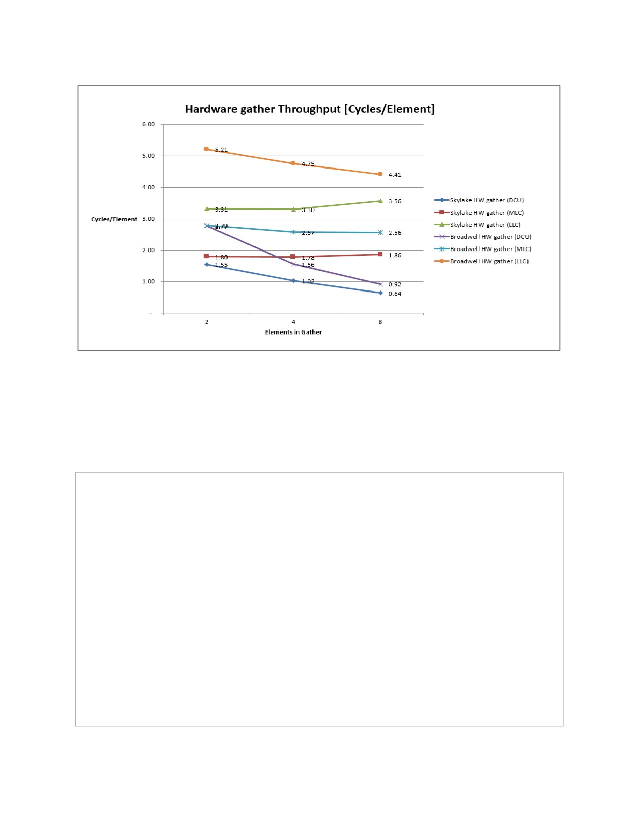
The throughput of GATHER instructions continue to improve from Broadwell to Skylake Microarchitec-
ture. This is shown in Figure 15-4.
15-67
OPTIMIZATIONS FOR INTEL® AVX, INTEL® AVX2, AND INTEL® FMA
Figure 15-4. Throughput Comparison of Gather Instructions
Example 15-45 gives the asm sequence of software implementation that is equivalent to the VPGATHERD
instruction. This can be used to compare the trade-off of using a hardware gather instruction or software
gather sequence based on inserting an individual element.
Example 15-45. Software AVX Sequence Equivalent to Full-Mask VPGATHERD
mov eax, [rdi]
// load index0
vmovd xmm0, [rsi+4*rax]
// load element0
mov eax, [rdi+4]
// load index1
vpinsrd xmm0, xmm0, [rsi+4*rax], 0x1
// load element1
mov eax, [rdi+8]
// load index2
vpinsrd xmm0, xmm0, [rsi+4*rax], 0x2
// load element2
mov eax, [rdi+12]
// load index3
vpinsrd xmm0, xmm0, [rsi+4*rax], 0x3
// load element3
mov eax, [rdi+16]
// load index4
vmovd xmm1, [rsi+4*rax]
// load element4
mov eax, [rdi+20]
// load index5
vpinsrd xmm1, xmm1, [rsi+4*rax], 0x1
// load element5
mov eax, [rdi+24]
// load index6
vpinsrd xmm1, xmm1, [rsi+4*rax], 0x2
// load element6
mov eax, [rdi+28]
// load index7
vpinsrd xmm1, xmm1, [rsi+4*rax], 0x3
// load element7
vinserti128 ymm0, ymm0, xmm1, 1
//result in ymm0
15-68
OPTIMIZATIONS FOR INTEL® AVX, INTEL® AVX2, AND INTEL® FMA
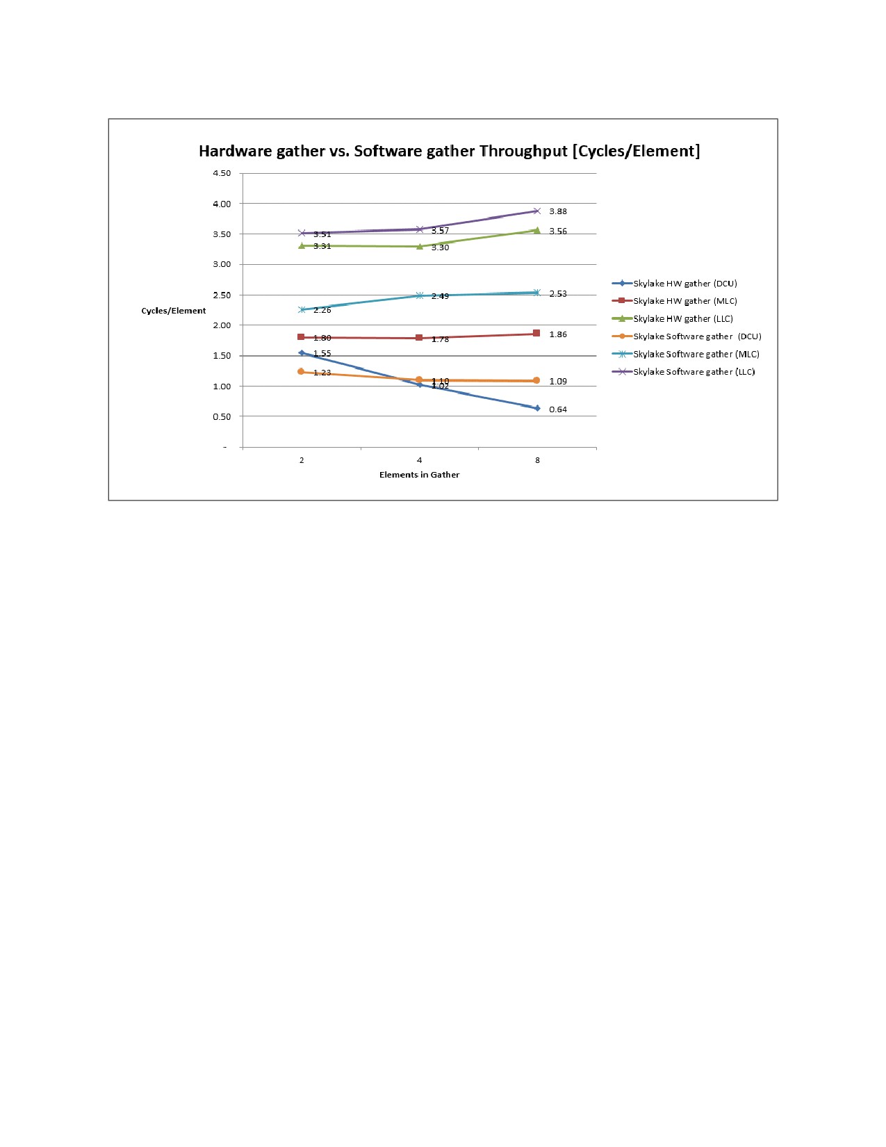
Figure 15-5. Comparison of HW GATHER Versus Software Sequence in Skylake Microarchitecture
Figure 15-5 compares per-element throughput using the VPGATHERD instruction versus a software
gather sequence with Skylake microarchitecture as a function of cache locality of data supply. With the
exception of using hardware GATHER on two data elements per instruction, the gather instruction out-
performs the software sequence on Skylake microarchitecture.
If data supply locality is from memory, software sequences are likely to perform better than the hardware
GATHER instruction.
15.16.4.1 Strided Loads
This section compares using the hardware GATHER instruction versus alternative implementations of
handling Array of Structures (AOS) to Structure of Arrays (SOA) transformation. The code separates the
real and imaginary elements in a complex array into two separate arrays.
C code:
for(int i=0;i<len;i++){
Real_buffer[i] = Complex_buffer[i].real;
Imaginary_buffer[i] = Complex_buffer[i].imag;
}
15-69

OPTIMIZATIONS FOR INTEL® AVX, INTEL® AVX2, AND INTEL® FMA
Example 15-46. AOS to SOA Transformation Alternatives
1: Scalar Code
2: AVX w/ VINSRT+VSHUFPS
3: AVX2 w/ VPGATHERD
loop:
loop:
loop:
lea eax, [r10+r10*1]
vmovdqu xmm0, xmmword ptr
lea r11, [r10+rcx*8]
movsxd rax, eax
[r10+rcx*8]
vpxor ymm5, ymm5, ymm5
inc r10d
vmovdqu xmm1, xmmword ptr
add rcx, 0x8
mov r11d, dword ptr [rsi+rax*8]
[r10+rcx*8+0x10]
vpxor ymm6, ymm6, ymm6
mov dword ptr [rcx+rax*4], r11d
vmovdqu xmm4, xmmword ptr
vmovdqa ymm3, ymm0
[r10+rcx*8+0x40]
mov r11d, dword ptr [rsi+rax*8+0x4]
vmovdqa ymm4, ymm0
vmovdqu xmm5, xmmword ptr
mov dword ptr [rdx+rax*4], r11d
vpgatherdd ymm5, ymmword ptr
[r10+rcx*8+0x50]
mov r11d, dword ptr [rsi+rax*8+0x8]
[r11+ymm2*4], ymm3
vinserti128 ymm2, ymm0, xmmword
mov dword ptr [rcx+rax*4+0x4],
vpgatherdd ymm6, ymmword ptr
ptr [r10+rcx*8+0x20], 0x1
r11d
[r11+ymm1*4], ymm4
vinserti128 ymm3, ymm1, xmmword
mov r11d, dword ptr [rsi+rax*8+0xc]
vmovdqu ymmword ptr [r9], ymm5
ptr [r10+rcx*8+0x30], 0x1
mov dword ptr [rdx+rax*4+0x4],
vmovdqu ymmword ptr [r8], ymm6
vinserti128 ymm6, ymm4, xmmword
r11d
add r9, 0x20
ptr [r10+rcx*8+0x60], 0x1
cmp r10d, r8d
add r8, 0x20
vinserti128 ymm7, ymm5, xmmword
jl loop
cmp rcx, rsi
ptr [r10+rcx*8+0x70], 0x1
jl loop
add rcx, 0x10
vshufps ymm0, ymm2, ymm3, 0x88
vshufps ymm1, ymm2, ymm3, 0xdd
vshufps ymm4, ymm6, ymm7, 0x88
vshufps ymm5, ymm6, ymm7, 0xdd
vmovups ymmword ptr [r9], ymm0
vmovups ymmword ptr [r8], ymm1
vmovups ymmword ptr [r9+0x20],
ymm4
vmovups ymmword ptr [r8+0x20],
ymm5
add r9, 0x40
add r8, 0x40
cmp rcx, rsi
jl loop
With strided access patterns, an AVX software sequence can load and shuffle on multiple elements and is
the more optimal technique.
Table 15-7. Comparison of AOS to SOA with Strided Access Pattern
Microarchitecture
Scalar
VPGATHERD
AVX VINSRTF128/VSHUFFLEPS
Broadwell
1X
1.7X
4.8X
Skylake
1X
2.7X
4.9X
15.16.4.2 Adjacent Loads
This section compares using the hardware GATHER instruction versus alternative implementations of
handling a variant situation of AOS to SOA transformation. In this case, AOS data are not loaded sequen-
tially but via an index array.
15-70

OPTIMIZATIONS FOR INTEL® AVX, INTEL® AVX2, AND INTEL® FMA
C code:
for(int i=0;i<len;i++){
Real_buffer[i] = Complex_buffer[Index_buffer[i]].real;
Imaginary_buffer[i] = Complex_buffer[Index_buffer[i]].imag;
}
Example 15-47. Non-Strided AOS to SOA
AVX2 GATHERPD
AVX VINSRTF128 /UNPACK
loop:
loop:
vmovdqu ymm1, ymmword ptr [rsi+rdx*4]
movsxd r10, dword ptr [rdx+rsi*4]
vpaddd ymm3, ymm1, ymm1
shl r10, 0x4
vpaddd ymm14, ymm13, ymm3
movsxd r11, dword ptr [rdx+rsi*4+0x8]
vxorpd ymm5, ymm5, ymm5
shl r11, 0x4
vmovdqa ymm2, ymm0
vmovupd xmm0, xmmword ptr [r9+r10*1]
vxorpd ymm6, ymm6, ymm6
movsxd r10, dword ptr [rdx+rsi*4+0x4]
vmovdqa ymm4, ymm0
shl r10, 0x4
vxorpd ymm10, ymm10, ymm10
vinsertf128 ymm2, ymm0, xmmword ptr [r9+r11*1], 0x1
vmovdqa ymm7, ymm0
vmovupd xmm1, xmmword ptr [r9+r10*1]
vxorpd ymm11, ymm11, ymm11
movsxd r10, dword ptr [rdx+rsi*4+0xc]
vmovdqa ymm9, ymm0
shl r10, 0x4
vextracti128 xmm12, ymm14, 0x1
vinsertf128 ymm3, ymm1, xmmword ptr [r9+r10*1], 0x1
vextracti128 xmm8, ymm3, 0x1
movsxd r10, dword ptr [rdx+rsi*4+0x10]
vgatherdpd ymm6, ymmword ptr[r8+xmm8*8],ymm4
shl r10, 0x4
vgatherdpd ymm5, ymmword ptr[r8+xmm3*8],ymm2
vunpcklpd ymm4, ymm2, ymm3
vmovupd ymmword ptr [rcx+rdx*8], ymm5
vunpckhpd ymm5, ymm2, ymm3
vmovupd ymmword ptr [rcx+rdx*8+0x20], ymm6
vmovupd ymmword ptr [rcx], ymm4
vgatherdpd ymm11, ymmword ptr[r8+xmm12*8],ymm7
vmovupd xmm6, xmmword ptr [r9+r10*1]
vgatherdpd ymm10, ymmword ptr[r8+xmm14*8],ymm9
vmovupd ymmword ptr [rax], ymm5
vmovupd ymmword ptr [rax+rdx*8], ymm10
movsxd r10, dword ptr [rdx+rsi*4+0x18]
vmovupd ymmword ptr [rax+rdx*8+0x20], ymm11
shl r10, 0x4
add rdx, 0x8
vinsertf128 ymm8, ymm6, xmmword ptr [r9+r10*1], 0x1
cmp rdx, r11
movsxd r10, dword ptr [rdx+rsi*4+0x14]
jb loop
shl r10, 0x4
vmovupd xmm7, xmmword ptr [r9+r10*1]
movsxd r10, dword ptr [rdx+rsi*4+0x1c]
add rsi, 0x8
shl r10, 0x4
vinsertf128 ymm9, ymm7, xmmword ptr [r9+r10*1], 0x1
vunpcklpd ymm10, ymm8, ymm9
vunpckhpd ymm11, ymm8, ymm9
vmovupd ymmword ptr [rcx+0x20], ymm10
add rcx, 0x40
vmovupd ymmword ptr [rax+0x20], ymm11
add rax, 0x40
cmp rsi, r8
jl loop
15-71

OPTIMIZATIONS FOR INTEL® AVX, INTEL® AVX2, AND INTEL® FMA
With non-strided, regular access pattern of AOS to SOA, an AVX software sequence that uses
VINSERTF128 and interleaved packing of multiple elements can be more optimal.
Table 15-8. Comparison of Indexed AOS to SOA Transformation
Microarchitecture
VPGATHERPD
AVX VINSRTF128/VUNPCK*
Broadwell
1X
1.4X
Skylake
1.3X
1.7X
15.16.5 AVX2 Conversion Remedy to MMX Instruction Throughput Limitation
In processors based on the Skylake microarchitecture, the functionality of the MMX instruction set is
unchanged from prior generations. But many MMX instructions are constrained to execute to one port
with half the instruction throughput relative to prior microarchitectures. The MMX instructions with
throughput constraints include:
• PADDS[B/W], PADDUS[B/W], PSUBS[B/W], PSUBUS[B/W].
• PCMPGT[B/W/D], PCMPEQ[B/W/D].
• PMAX[UB/SW], PMIN[UB/SW].
• PAVG[B/W], PABS[B/W/D], PSIGN[B/W/D].
To overcome the reduction of MMX instruction throughput, conversion of asm and intrinsic code to use
AVX2 instruction will provide significant performance improvements. Example 15-48 shows the asm
sequence using AVX2 versus MMX equivalent. In Skylake microarchitecture, the MMX code shown in
Example 15-48 will execute at approximately half the speed relative to the Broadwell microarchitecture.
This is due to PMAXSW/PMINSW throughput being reduced by half with the single-port restriction. When
the same task is implemented with the equivalent AVX2 sequence, the performance of the AVX2 code on
Skylake microarchitecture will be ~3.9X of the MMX code executing on the Broadwell microarchitecture.
15-72

OPTIMIZATIONS FOR INTEL® AVX, INTEL® AVX2, AND INTEL® FMA
Example 15-48. Conversion to Throughput-Reduced MMX sequence to AVX2 Alternative
MMX Code
AVX2 Code
mov rax, pIn
mov rax, pIn
mov rbx, pOut
mov rbx, pOut
mov r8, len
mov r8, len
mov rcx, 8
mov rcx, 32
movq mm0, [rax]
vmovdqu ymm0, ymmword ptr [rax]
movq mm1, [rax + 8]
vmovdqu ymm1, ymmword ptr [rax + 32]
movq mm2, mm0
vmovdqu ymm2, ymm0
movq mm3, mm1
vmovdqu ymm3, ymm1
cmp rcx, r8
cmp rcx, r8
jge end
jge end
loop:
loop:
movq mm4, [rax + 2*rcx]
vmovdqu ymm4, ymmword ptr [rax + 2*rcx]
movq mm5, [rax + 2*rcx + 8]
vmovdqu ymm5, ymmword ptr [rax + 2*rcx + 32]
vpmaxsw ymm0, ymm0, ymm4
pmaxsw mm0, mm4
vpmaxsw ymm1, ymm1, ymm5
pmaxsw mm1, mm5
vpminsw ymm2, ymm2, ymm4
pminsw mm2, mm4
vpminsw ymm3, ymm3, ymm5
pminsw mm3, mm5
add rcx, 32
add rcx, 8
cmp rcx, r8
cmp rcx, r8
jl loop
jl loop
end:
//Reduction
end:
vpmaxsw ymm0, ymm0, ymm1
//Reduction
vextracti128 xmm1, ymm0, 1
pmaxsw mm0, mm1
vpmaxsw xmm0, xmm0, xmm1
pshufw mm1, mm0, 0xE
vpshufd xmm1, xmm0, 0xe
pmaxsw mm0, mm1
vpmaxsw xmm0, xmm0, xmm1
pshufw mm1, mm0, 1
vpshuflw xmm1, xmm0, 0xe
pmaxsw mm0, mm1
vpmaxsw xmm0, xmm0, xmm1
vpshuflw xmm1, xmm0, 1
pminsw mm2, mm3
vpmaxsw xmm0, xmm0, xmm1
pshufw mm3, mm2, 0xE
vmovd eax, xmm0
pminsw mm2, mm3
mov word ptr [rbx], ax
pshufw mm3, mm2, 1
vpminsw ymm2, ymm2, ymm3
pminsw mm2, mm3
vextracti128 xmm1, ymm2, 1
vpminsw xmm2, xmm2, xmm1
movd eax, mm0
vpshufd xmm1, xmm2, 0xe
mov WORD PTR [rbx], ax
vpminsw xmm2, xmm2, xmm1
movd eax, mm2
vpshuflw xmm1, xmm2, 0xe
mov WORD PTR [rbx + 2], ax
vpminsw xmm2, xmm2, xmm1
emms
vpshuflw xmm1, xmm2, 1
vpminsw xmm2, xmm2, xmm1
vmovd eax, xmm2
mov word ptr [rbx + 2], ax
15-73
OPTIMIZATIONS FOR INTEL® AVX, INTEL® AVX2, AND INTEL® FMA
15-74
8.
Updates to Chapter 18
Change bars and violet text show changes to Chapter 18 of the Intel® 64 and IA-32 Architectures Optimization
Reference Manual: Software Optimization for Intel AVX-512 Instructions.
------------------------------------------------------------------------------------------
Changes to this chapter:
• Example 18-1: Corrected typos: Teta with theta.
• Example 18-2: Corrected typos: Teta with theta.
Intel® 64 and IA-32 Architectures Optimization Reference Manual Documentation Changes
13

CHAPTER 18
SOFTWARE OPTIMIZATION FOR INTEL® AVX-512 INSTRUCTIONS
Intel® Advanced Vector Extensions 512 (Intel® AVX-512) are the following set of 512-bit instruction set
extensions supported by recent microarchitectures, beginning with Skylake server microarchitecture,
and the Intel® Xeon Phi™ processors based on Knights Landing microarchitecture.
• Intel® AVX-512 Foundation (F)
— 512-bit vector width.
— 32 512-bit long vector registers.
— Data expand and data compress instructions.
— Ternary logic instruction.
— 8 new 64-bit long mask registers.
— Two source cross-lane permute instructions.
— Scatter instructions.
— Embedded broadcast/rounding.
— Transcendental support.
• Intel® AVX-512 Conflict Detection Instructions (CD)
• Intel® AVX-512 Exponential and Reciprocal Instructions (ER)
• Intel® AVX-512 Prefetch Instructions (PF)
• Intel® AVX-512 Byte and Word Instructions (BW)
• Intel® AVX-512 Double Word and Quad Word Instructions (DQ)
— New QWORD and Compute and Convert Instructions.
• Intel® AVX-512 Vector Length Extensions (VL)
The Venn diagram below shows the different extensions supported by the two processor families.
Processors based on Skylake
Intel® Xeon Phi™ Processor
Server Microarchitecture
Intel AVX-512 BW
Intel AVX-512 F
Intel AVX-512 ER
Intel AVX-512 DQ
Intel AVX-512 CD
Intel AVX-512 PF
Intel AVX-512 VL
SOM00001
Figure 18-1. Intel® AVX-512 Extensions Supported by Skylake Server Microarchitecture and Knights
Landing Microarchitecture

SOFTWARE OPTIMIZATION FOR INTEL® AVX-512 INSTRUCTIONS
Performance reports in this chapter are based on Data Cache Unit (DCU) resident data measurements on
the Skylake Server System with Intel® Turbo-Boost technology disabled, Intel® SpeedStep® Technology
disabled, core and uncore frequency set to 1.8GHz, unless otherwise specified. This fixed frequency
configuration is used in order to isolate code change impacts from other factors. See Section 2.5.3,
“Skylake Server Power Management”, to understand the power and frequency impacts of using Intel
AVX-512.
18.1
BASIC INTEL® AVX-512 VS. INTEL® AVX2 CODING
In most cases, the main performance driver for Intel AVX-512 will be the 512-bit register width. This
section demonstrates the similarity and differences between basic Intel AVX2 and Intel AVX-512 code
and explains how to convert code from Intel AVX2 to Intel AVX-512 easily. The first sub section demon-
strates the conversion of intrinsic code and the second sub-section of assembly code. The following
sections highlight advanced aspects that require consideration and treatment when doing such conver-
sions.
The examples in the following subsections implement a Cartesian coordinate system rotation. A point in
a Cartesian coordinate system is described by the pair (x,y). The following picture demonstrates a Carte-
sian rotation of (x,y) by angle to (x',y').
Y
Y’
X’
θ
X
x‘ = xcosθ - ysinθ
y‘ = xsinθ + ycosθ
Y5
X
5
Y5
X5
Y5
X5
Y5
X5
Y5
X5
Y5
X5
: In Buffer
Y’5
X’5
Y’4
X’4
Y’3
X’3
Y’2
X’2
Y’1
X’1
Y’0
X’0
s*X5
s*X5
s*X4
s*X4
s*X3
s*X3
s*X2
s*X2
s*X1
s*X1
s*X0
s*X0
+
-
+
-
+
-
+
-
+
-
+
-
: Out Buffer
c*Y5
c*Y5
c*Y4
c*Y4
c*Y3
c*Y3
c*Y2
c*Y2
c*Y1
c*Y1
c*Y0
c*Y0
*c = cosθ
s = sinθ
SOM00002
Figure 18-2. Cartesian Rotation
18.1.1 Intrinsic Coding
The following comparison of Intel AVX2 and Intel AVX-512 shows how to convert a simple intrinsic Intel
AVX2 code sequence to Intel AVX-512. This example demonstrates the Intel AVX Instruction format, 64
byte ZMM registers, dynamic and static memory allocation with data alignment of 64bytes, and the C
data type representing 16 floating point elements in a ZMM register. Follow these guidelines when doing
this transformation.
18-2

SOFTWARE OPTIMIZATION FOR INTEL® AVX-512 INSTRUCTIONS
• Align statically and dynamically allocated buffers to 64-bytes.
• Use a double supplemental buffer size for constants.
• Change __mm256_ intrinsic name prefix with __mm512_.
• Change variable data types names from __m256 to __m512.
• Divide by 2 iteration count (double stride length).
Example 18-1. Cartesian Coordinate System Rotation with Intrinsics
Intel® AVX2 Intrinsics Code
Intel® AVX-512 Intrinsics Code
#include <immintrin.h>
#include <immintrin.h>
int main()
int main()
{
{
int len = 3200;
int len = 3200;
//Dynamic memory allocation with 32byte
//Dynamic memory allocation with 64byte
//alignment
//alignment
float* pInVector = (float *)
float* pInVector = (float *)
_mm_malloc(len*sizeof(float),32);
_mm_malloc(len*sizeof(float),64);
float* pOutVector = (float *)
float* pOutVector = (float *)
_mm_malloc(len*sizeof(float),32);
_mm_malloc(len*sizeof(float),64);
//init data
//init data
for (int i=0; i<len; i++)
for (int i=0; i<len; i++)
pInVector[i] = 1;
pInVector[i] = 1;
float cos_theta = 0.8660254037;
float cos_theta = 0.8660254037;
float sin_theta = 0.5;
float sin_theta = 0.5;
//Static memory allocation of 8 floats with 32byte align-
//Static memory allocation of 16 floats with 64byte align-
ments
ments
__declspec(align(32)) float cos_sin_theta_vec[8] =
__declspec(align(64)) float cos_sin_theta_vec[16] =
{cos_theta, sin_theta, cos_theta, sin_theta, cos_theta,
{cos_theta, sin_theta, cos_theta, sin_theta, cos_theta,
sin_theta, cos_theta, sin_theta};
sin_theta, cos_theta, sin_theta cos_theta, sin_theta,
cos_theta, sin_theta, cos_theta, sin_theta, cos_theta,
sin_theta};
__declspec(align(32)) float sin_cos_theta_vec[8] =
__declspec(align(64)) float sin_cos_theta_vec[16] =
{sin_theta, cos_theta, sin_theta, cos_theta, sin_theta,
{sin_theta, cos_theta, sin_theta, cos_theta, sin_theta,
cos_theta, sin_theta, cos_theta};
cos_theta, sin_theta, cos_theta, sin_theta, cos_theta,
sin_theta, cos_theta, sin_theta, cos_theta, sin_theta,
cos_theta};
//__m256 data type represents a Ymm
// register with 8 float elements
//__m512 data type represents a Zmm
__m256 Ymm_cos_sin = _mm256_-
// register with 16 float elements
load_ps(cos_sin_theta_vec);
__m512 Zmm_cos_sin = _mm512_-
load_ps(cos_sin_theta_vec);
18-3

SOFTWARE OPTIMIZATION FOR INTEL® AVX-512 INSTRUCTIONS
Example 18-1. Cartesian Coordinate System Rotation with Intrinsics (Contd.)
//Intel® AVX2 256bit packed single load
//Intel® AVX-512 512bit packed single load
__m256 Ymm_sin_cos = _mm256_-
__m512 Zmm_sin_cos = _mm512_-
load_ps(sin_cos_theta_vec);
load_ps(sin_cos_theta_vec);
__m512 Zmm0, Zmm1, Zmm2, Zmm3;
__m256 Ymm0, Ymm1, Ymm2, Ymm3;
//processing 32 elements in an unrolled
//processing 16 elements in an unrolled
//twice loop
//twice loop
for(int i=0; i<len; i+=32)
for(int i=0; i<len; i+=16)
{
{
Zmm0 = _mm512_load_ps(pInVector+i);
Ymm0 = _mm256_load_ps(pInVector+i);
Zmm1 = _mm512_moveldup_ps(Zmm0);
Ymm1 = _mm256_moveldup_ps(Ymm0);
Zmm2 = _mm512_movehdup_ps(Zmm0);
Ymm2 = _mm256_movehdup_ps(Ymm0);
Zmm2 = _mm512_mul_ps(Zmm2,Zmm_sin_cos);
Ymm2 = _mm256_mul_ps(Ymm2,Ymm_sin_cos);
Zmm3 =
Ymm3 =
_mm512_fmaddsub_ps(Zmm1,Zmm_cos_sin,Zmm2);
_mm256_fmaddsub_ps(Ymm1,Ymm_cos_sin,Ymm2);
_mm512_store_ps(pOutVector + i,Zmm3);
_mm256_store_ps(pOutVector + i,Ymm3);
Zmm0 = _mm512_load_ps(pInVector+i+16);
Ymm0 = _mm256_load_ps(pInVector+i+8);
Zmm1 = _mm512_moveldup_ps(Zmm0);
Ymm1 = _mm256_moveldup_ps(Ymm0);
Zmm2 = _mm512_movehdup_ps(Zmm0);
Ymm2 = _mm256_movehdup_ps(Ymm0);
Zmm2 = _mm512_mul_ps(Zmm2, Zmm_sin_cos);
Ymm2 = _mm256_mul_ps(Ymm2, Ymm_sin_cos);
Zmm3 =
Ymm3 =
_mm512_fmaddsub_ps(Zmm1,Zmm_cos_sin,Zmm2);
_mm256_fmaddsub_ps(Ymm1,Ymm_cos_sin,Ymm2);
_mm512_store_ps(pOutVector+i+16,Zmm3);
_mm256_store_ps(pOutVector+i+8,Ymm3);
}
}
_mm_free(pInVector);
_mm_free(pOutVector);
_mm_free(pInVector);
_mm_free(pOutVector);
return 0;
}
return 0;
}
Baseline
Speedup: 1.95x
18.1.2 Assembly Coding
Similar to the intrinsic porting guidelines, assembly porting guidelines are listed below:
• Align statically and dynamically allocated buffers to 64-bytes.
• Double the supplemental buffer sizes if needed.
• Add a “v” prefix to instruction names.
• Change register names from ymm to zmm.
• Divide the iteration count by two (or double stride length).
18-4

SOFTWARE OPTIMIZATION FOR INTEL® AVX-512 INSTRUCTIONS
Example 18-2. Cartesian Coordinate System Rotation with Assembly
Intel® AVX2 Assembly Code
Intel® AVX-512 Assembly Code
#include <immintrin.h>
#include <immintrin.h>
int main()
int main()
{
{
int len = 3200;
int len = 3200;
//Dynamic memory allocation with 32byte alignment
//Dynamic memory allocation with 64byte alignment
float* pInVector = (float *)
float* pInVector = (float *)
_mm_malloc(len*sizeof(float),32);
_mm_malloc(len*sizeof(float),64);
float* pOutVector = (float *)
float* pOutVector = (float *)
_mm_malloc(len*sizeof(float),32);
_mm_malloc(len*sizeof(float),64);
//init data
//init data
for (int i=0; i<len; i++)
for (int i=0; i<len; i++)
pInVector[i] = 1;
pInVector[i] = 1;
float cos_theta = 0.8660254037;
float cos_theta = 0.8660254037;
float sin_theta = 0.5;
float sin_theta = 0.5;
//Static memory allocation of 8 floats with 32byte align-
//Static memory allocation of 16 floats with 64byte align-
ments
ments
__declspec(align(32)) float cos_sin_theta_vec[8] =
__declspec(align(64)) float cos_sin_theta_vec[16] =
{cos_theta, sin_theta,
{cos_theta,
cos_theta, sin_theta, cos_theta, sin_theta, cos_theta,
sin_theta, cos_theta, sin_theta, cos_theta, sin_theta,
sin_theta};
cos_theta, sin_theta, cos_theta, sin_theta, cos_theta,
sin_theta, cos_theta, sin_theta, cos_theta, sin_theta};
__declspec(align(64)) float sin_cos_theta_vec[16] =
__declspec(align(32)) float sin_cos_theta_vec[8] =
{sin_theta, cos_theta, sin_theta, cos_theta, sin_theta,
{sin_theta, cos_theta, sin_theta, cos_theta, sin_theta,
cos_theta, sin_theta cos_theta, sin_theta, cos_theta,
cos_theta, sin_theta, cos_theta};
sin_theta, cos_theta, sin_theta, cos_theta, sin_theta,
cos_theta};
__asm
__asm
{
{
mov rax,pInVector
mov rax,pInVector
mov r8,pOutVector
mov r8,pOutVector
// Load into a zmm register of 64 bytes
// Load into a ymm register of 32 bytes
vmovups zmm3, zmmword ptr[cos_sin_theta_vec]
vmovups ymm3, ymmword ptr[cos_sin_theta_vec]
vmovups zmm4, zmmword ptr[sin_cos_theta_vec]
vmovups ymm4, ymmword ptr[sin_cos_theta_vec]
mov edx, len
mov edx, len
shl edx, 2
shl edx, 2
xor ecx, ecx
xor ecx, ecx
loop1:
loop1:
vmovsldup zmm0, [rax+rcx]
vmovsldup ymm0, [rax+rcx]
vmovshdup zmm1, [rax+rcx]
vmovshdup ymm1, [rax+rcx]
vmulps zmm1, zmm1, zmm4
vmulps ymm1, ymm1, ymm4
vfmaddsub213ps zmm0, zmm3, zmm1
vfmaddsub213ps ymm0, ymm3, ymm1
// 64 byte store from a zmm register
// 32 byte store from a ymm register
vmovaps [r8+rcx], zmm0
vmovaps [r8+rcx], ymm0
18-5

SOFTWARE OPTIMIZATION FOR INTEL® AVX-512 INSTRUCTIONS
Example 18-2. Cartesian Coordinate System Rotation with Assembly (Contd.)
vmovsldup ymm0, [rax+rcx+32]
vmovsldup zmm0, [rax+rcx+64]
vmovshdup ymm1, [rax+rcx+32]
vmovshdup zmm1, [rax+rcx+64]
vmulps ymm1, ymm1, ymm4
vmulps zmm1, zmm1, zmm4
vfmaddsub213ps ymm0, ymm3, ymm1
vfmaddsub213ps zmm0, zmm3, zmm1
// offset 32 bytes from previous store
// offset 64 bytes from previous store
vmovaps [r8+rcx+32], ymm0
vmovaps [r8+rcx+64], zmm0
// Processed 64bytes in this loop
// Processed 128bytes in this loop
// (the code is unrolled twice)
// (the code is unrolled twice)
add ecx, 64
add ecx, 128
cmp ecx, edx
cmp ecx, edx
jl loop1
jl loop1
}
}
_mm_free(pInVector);
_mm_free(pInVector);
_mm_free(pOutVector);
_mm_free(pOutVector);
return 0;
return 0;
}
}
Baseline
Speedup: 1.95x
18.2
MASKING
Intel AVX-512 instructions which use the Extended VEX coding scheme (EVEX) encode a predicate
operand to conditionally control per-element computational operation and update the result to the desti-
nation operand. The predicate operand is known as the opmask register. The opmask is a set of eight
architectural registers, 64 bits each. From this set of 8 architectural registers, only k1 through k7 can be
addressed as the predicate operand; k0 can be used as a regular source or destination but cannot be
encoded as a predicate operand.
A predicate operand can be used to enable memory fault-suppression for some instructions with a
memory source operand.
As a predicate operand, the opmask registers contain one bit to govern the operation / update of each
data element of a vector register. Masking is supported on Skylake microarchitecture for instructions with
all data sizes: byte (int8), word (int16), single precision floating-point (float32), integer doubleword
(int32), double precision floating-point (float64), integer quadword (int64). Therefore, a vector register
holds either 8, 16, 32 or 64 elements; accordingly, the length of a vector mask register is 64 bits.
Masking on Skylake microarchitecture is also enabled for all vector length values: 128-bit, 256-bit and
512-bit. Each instruction accesses only the number of least significant mask bits needed based on its
data type and vector length. For example, Intel AVX-512 instructions operating on 64-bit data elements
with a 512-bit vector length, only use the 8 (i.e., 512/64) least significant bits of the opmask register.
An opmask register affects an Intel AVX-512 instruction at per-element granularity. So, any numeric or
non-numeric operation of each data element and per-element updates of intermediate results to the
destination operand are predicated on the corresponding bit of the opmask register.
18-6

SOFTWARE OPTIMIZATION FOR INTEL® AVX-512 INSTRUCTIONS
An opmask serving as a predicate operand in Intel AVX-512 has the following properties:
• The instruction's operation is only performed for an element if the corresponding opmask bit is set.
This implies that no exception or violation can be caused by an operation on a masked-off element.
Consequently, no MXCSR exception flag is updated as a result of a masked-off operation.
• A destination element is not updated with the result of the operation if the corresponding writemask
bit is not set. Instead, the destination element value may be preserved (merging-masking) or zeroed
out (zeroing-masking).
• For some instructions with a memory operand, memory faults are suppressed for elements with a
mask bit of 0.
Note that this feature provides a powerful construct to implement control-flow predication, since the
mask provides a merging behavior for Intel AVX-512 vector register destinations. As an alternative the
masking can be used for zeroing instead of merging, so that the masked out elements are updated with
0 instead of preserving the old value. The zeroing behavior removes the implicit dependency on the old
value when it is not needed.
Most instructions with masking enabled accept both forms of masking. Instructions that must have
EVEX.aaa bits different than 0 (gather and scatter) and instructions that write to memory, only accept
merging-masking.
The per-element destination update rule also applies when the destination operand is a memory location.
Vectors are written on a per element basis, based on the opmask register used as a predicate operand.
The value of an opmask register can be:
• Generated as a result of a vector instruction (CMP, FPCLASS, etc.).
• Loaded from memory.
• Loaded from GPR register.
• Modified by mask-to-mask operations.
18.2.1 Masking Example
The masked instructions conditionally operate with packed data elements, depending on the mask bits
associated with each data element. The mask bit for each data element is the corresponding bit in the
mask register.
When performing a mask instruction, the returned value is 0 for elements which have a corresponding
mask value of 0. The corresponding value in the destination register depends on the zeroing flag:
• If the flag is set, the memory location is filled with zeros.
• If the flag is not set, the values in memory location can are preserved.
The following figures show an example for a mask move from one register to another when using
merging masking.
vmovaps zmm1 {k1}, zmm0
The destination register before instruction execution is shown below.
63 32
31
0
bits
b15
b14
b13
b12
b11
b10
b9
b8
b7
b6
b5
b4
b3
b2
b1
b0
ZMM1
SOM00003
18-7
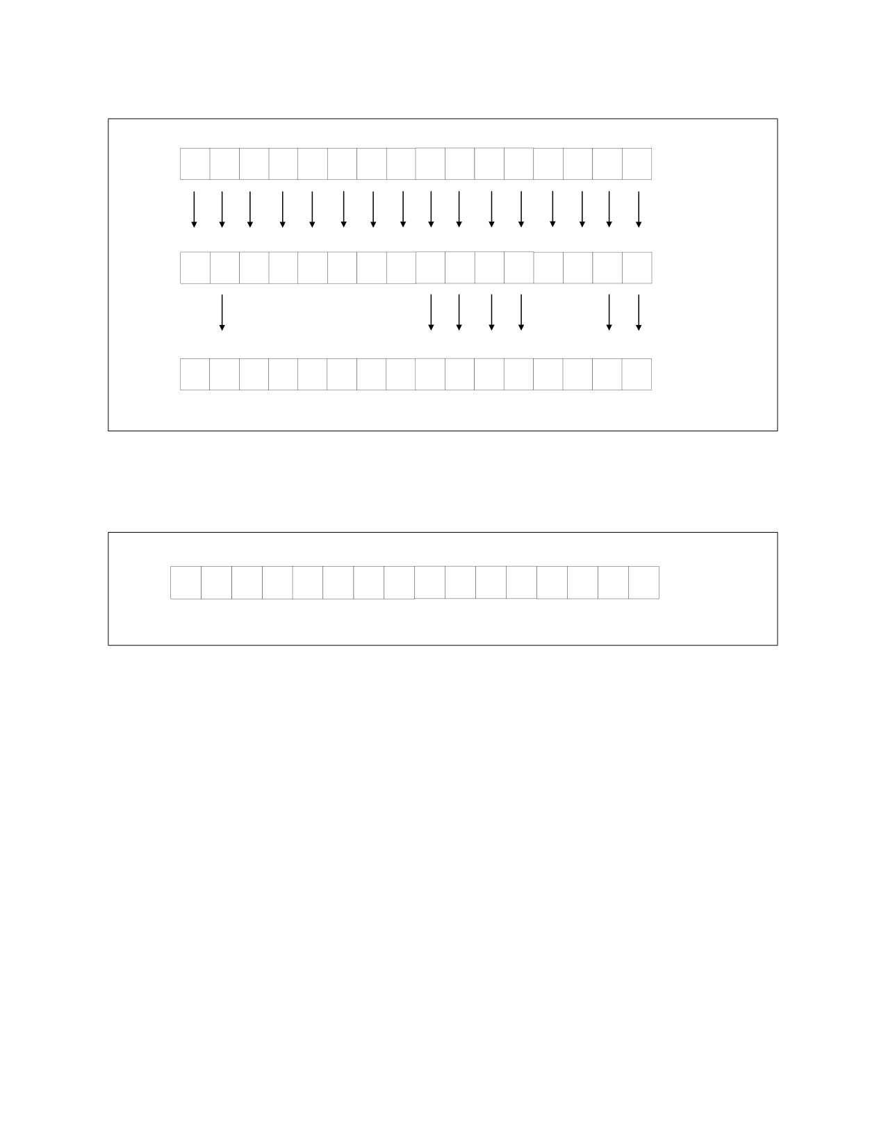
SOFTWARE OPTIMIZATION FOR INTEL® AVX-512 INSTRUCTIONS
Operation is as follows.
… 63 32 31
0 bits
a15
a14
a13
a12
a11
a10
a9
a8
a7
a6
a5
a4
a3
a2
a1
a0
ZMM0
…
5
4
3
2
1
0
bits
0
1
0
0
0
0
0
0
1
1
1
1
0
0
1
1
K1
… 63 32 31
0 bits
b15
a14
b13
b12
b11
b10
b9
b8
a7
a6
a5
a4
b3
b2
a1
a0
ZMM1
SOM00004
The result of the execution with zeroing masking is (notice the {z} in the instruction):
vmovaps zmm1 {k1}{z}, zmm0
… 63 32 31
0 bits
0
a14
0
0
0
0
0
0
a7
a6
a5
a4
0
0
a1
a0
ZMM1
SOM00005
Notice that merging masking operations has a dependency on the destination, but zeroing masking is
free of such dependency.
The following example shows how masking could be done with Intel AVX-512 in contrast to Intel AVX2.
C Code:
const int N = miBufferWidth;
const double* restrict a = A;
const double* restrict b = B;
double* restrict c = Cref;
for (int i = 0; i < N; i++){
double res = b[i];
if(a[i] > 1.0){
res = res * a[i];
}
c[i] = res;
}
18-8

SOFTWARE OPTIMIZATION FOR INTEL® AVX-512 INSTRUCTIONS
Example 18-3. Masking with Intrinsics
Intel® AVX2 Intrinsics Code
Intel® AVX-512 Intrinsics Code
for (int i = 0; i < N; i+=32){
for (int i = 0; i < N; i+=32){
__m256d aa, bb, mask;
__m512d aa, bb;
#pragma unroll(8)
__mmask8 mask;
for (int j = 0; j < 8; j++){
#pragma unroll(4)
aa
= _mm256_loadu_pd(a+i+j*4);
for (int j = 0; j < 4; j++){
bb
= _mm256_loadu_pd(b+i+j*4);
aa
= _mm512_loadu_pd(a+i+j*8);
mask = _mm256_c-
bb
= _mm512_loadu_pd(b+i+j*8);
mp_pd(_mm256_set1_pd(1.0), aa, 1);
mask = _mm512_cmp_p-
aa
= _mm256_and_pd(aa, mask); // zero the
d_mask(_mm512_set1_pd(1.0), aa, 1);
false values
bb
= _mm512_mask_mul_pd(bb, mask, aa,
aa
= _mm256_mul_pd(aa, bb);
bb);
bb
= _mm256_blendv_pd(bb, aa, mask);
_mm512_storeu_pd(c+8*j, bb);
_mm256_storeu_pd(c+4*j, bb);
}
}
c += 32;
c += 32;
}
}
Baseline
Speedup: 2.9x
Example 18-4. Masking with Assembly
Intel® AVX2 Assembly Code
Intel® AVX-512 Assembly Code
mov rax, a
mov rax, a
mov r11, b
mov r11, b
mov r8, N
mov r8, N
shr r8, 5
shr r8, 5
mov rsi, c
mov rsi, c
xor rcx, rcx
xor rcx, rcx
xor r9, r9
xor r9, r9
mov rdi, 1
loop:
cvtsi2sd xmm8, rdi
vmovupd ymm1, ymmword ptr [rax+rcx*8]
vbroadcastsd zmm8, xmm8
inc r9d
vmovupd ymm6, ymmword ptr [rax+rcx*8+0x20]
loop:
vmovupd ymm2, ymmword ptr [r11+rcx*8]
vmovups zmm0, zmmword ptr [rax+rcx*8]
vmovupd ymm7, ymmword ptr [r11+rcx*8+0x20]
inc r9d
vmovupd ymm11, ymmword ptr [rax+rcx*8+0x40]
vmovups zmm2, zmmword ptr [rax+rcx*8+0x40]
vmovupd ymm12, ymmword ptr [r11+rcx*8+0x40]
vmovups zmm4, zmmword ptr [rax+rcx*8+0x80]
vcmppd ymm4, ymm0, ymm1, 0x1
vmovups zmm6, zmmword ptr [rax+rcx*8+0xc0]
vcmppd ymm9, ymm0, ymm6, 0x1
vmovups zmm1, zmmword ptr [r11+rcx*8]
vcmppd ymm14, ymm0, ymm11, 0x1
vmovups zmm3, zmmword ptr [r11+rcx*8+0x40]
vandpd ymm16, ymm1, ymm4
vmovups zmm5, zmmword ptr [r11+rcx*8+0x80]
vandpd ymm17, ymm6, ymm9
vmovups zmm7, zmmword ptr [r11+rcx*8+0xc0]
18-9

SOFTWARE OPTIMIZATION FOR INTEL® AVX-512 INSTRUCTIONS
Example 18-4. Masking with Assembly (Contd.)
vmulpd ymm3, ymm16, ymm2
vcmppd k1, zmm8, zmm0, 0x1
vmulpd ymm8, ymm17, ymm7
vcmppd k2, zmm8, zmm2, 0x1
vmovupd ymm1, ymmword ptr [rax+rcx*8+0x60]
vcmppd k3, zmm8, zmm4, 0x1
vmovupd ymm6, ymmword ptr [rax+rcx*8+0x80]
vcmppd k4, zmm8, zmm6, 0x1
vblendvpd ymm5, ymm2, ymm3, ymm4
vmulpd zmm1{k1}, zmm0, zmm1
vblendvpd ymm10, ymm7, ymm8, ymm9
vmulpd zmm3{k2}, zmm2, zmm3
vmovupd ymm2, ymmword ptr [r11+rcx*8+0x60]
vmulpd zmm5{k3}, zmm4, zmm5
vmovupd ymm7, ymmword ptr [r11+rcx*8+0x80]
vmulpd zmm7{k4}, zmm6, zmm7
vmovupd ymmword ptr [rsi], ymm5
vmovups zmmword ptr [rsi], zmm1
vmovupd ymmword ptr [rsi+0x20], ymm10
vmovups zmmword ptr [rsi+0x40], zmm3
vcmppd ymm4, ymm0, ymm1, 0x1
vmovups zmmword ptr [rsi+0x80], zmm5
vcmppd ymm9, ymm0, ymm6, 0x1
vmovups zmmword ptr [rsi+0xc0], zmm7
vandpd ymm18, ymm11, ymm14
add rcx, 0x20
vandpd ymm19, ymm1, ymm4
add rsi, 0x100
vandpd ymm20, ymm6, ymm9
cmp r9d, r8d
vmulpd ymm13, ymm18, ymm12
jb loop
vmulpd ymm3, ymm19, ymm2
vmulpd ymm8, ymm20, ymm7
vmovupd ymm11, ymmword ptr [rax+rcx*8+0xa0]
vmovupd ymm1, ymmword ptr [rax+rcx*8+0xc0]
vmovupd ymm6, ymmword ptr [rax+rcx*8+0xe0]
vblendvpd ymm15, ymm12, ymm13, ymm14
vblendvpd ymm5, ymm2, ymm3, ymm4
vblendvpd ymm10, ymm7, ymm8, ymm9
vmovupd ymm12, ymmword ptr [r11+rcx*8+0xa0]
vmovupd ymm2, ymmword ptr [r11+rcx*8+0xc0]
vmovupd ymm7, ymmword ptr [r11+rcx*8+0xe0]
vmovupd ymmword ptr [rsi+0x40], ymm15
vmovupd ymmword ptr [rsi+0x60], ymm5
vmovupd ymmword ptr [rsi+0x80], ymm10
vcmppd ymm14, ymm0, ymm11, 0x1
vcmppd ymm4, ymm0, ymm1, 0x1
vcmppd ymm9, ymm0, ymm6, 0x1
vandpd ymm21, ymm11, ymm14
add rcx, 0x20
vandpd ymm22, ymm1, ymm4
vandpd ymm23, ymm6, ymm9
vmulpd ymm13, ymm21, ymm12
vmulpd ymm3, ymm22, ymm2
vmulpd ymm8, ymm23, ymm7
vblendvpd ymm15, ymm12, ymm13, ymm14
vblendvpd ymm5, ymm2, ymm3, ymm4
vblendvpd ymm10, ymm7, ymm8, ymm9
vmovupd ymmword ptr [rsi+0xa0], ymm15
vmovupd ymmword ptr [rsi+0xc0], ymm5
vmovupd ymmword ptr [rsi+0xe0], ymm10
add rsi, 0x100
cmp r9d, r8d
jb loop
Baseline
Speedup: 2.9x
18-10

SOFTWARE OPTIMIZATION FOR INTEL® AVX-512 INSTRUCTIONS
18.2.2 Masking Cost
Using masking may result in lower performance than the corresponding non-masked code. This may be
caused by one of the following situations:
• An additional blend operation on each load.
• Dependency on the destination when using merge masking. This dependency does not exist when
using zero masking.
• More restrictive masking forwarding rules (see Forwarding and Memory Masking for more infor-
mation).
The following example shows how using merge masking creates a dependency on the destination
register.
Example 18-5. Masking Example
No Masking
Merge Masking
Zero Masking
mov rbx, iter
mov rbx, iter
mov rbx, iter
loop:
loop:
loop:
vmulps zmm0, zmm9, zmm8
vmulps zmm0{k1}, zmm9, zmm8
vmulps zmm0{k1}{z}, zmm9, zmm8
vmulps zmm1, zmm9, zmm8
vmulps zmm1{k1}, zmm9, zmm8
vmulps zmm1{k1}{z}, zmm9, zmm8
dec rbx
dec rbx
dec rbx
jnle loop
jnle loop
jnle loop
Baseline
Slowdown: 4x
Slowdown: Equal to baseline.
With no masking, the processor executes 2 multiplies per cycle on a 2 FMA server.
With merge masking, the processor executes 2 multiplies every 4 cycles as the multiplies in iteration N
depend on the output of the multiplies in iteration N-1.
Zero masking does not have a dependency on the destination register and therefore can execute 2 multi-
plies per cycle on a 2 FMA server.
Recommendation: Masking has a cost, so use it only when necessary. When possible, use zero
masking rather than merge masking.
18.2.3 Masking vs. Blending
This section discusses the advantages and disadvantages of using blending vs. masking for conditional
code.
Consider the following code:
for ( i=0; i<SIZE; i++ )
{
if ( a[i] > 0 )
{
b[i] *= 2;
}
else
{
b[i] /= 2;
}
}
18-11

SOFTWARE OPTIMIZATION FOR INTEL® AVX-512 INSTRUCTIONS
The example below shows two possible compilation alternatives of the code.
• Alternative 1 uses masked code and straight-forward arithmetic processing of data.
• Alternative 2 splits code to two independent unmasked flows that are processed one after another,
and then a masked move (blending), just before storing to memory.
Example 18-6. Masking vs. Blending Example 1
Alternative 1
Alternative 2
mov rax, pImage
mov rax, pImage
mov rbx, pImage1
mov rbx, pImage1
mov rcx, pOutImage
mov rcx, pOutImage
mov rdx, len
mov rdx, len
vpxord zmm0, zmm0, zmm0
vpxord zmm0, zmm0, zmm0
mainloop:
mainloop:
vmovdqa32 zmm2, [rax+rdx*4-0x40]
vmovdqa32 zmm2, [rax+rdx*4-0x40]
vmovdqa32 zmm1, [rbx+rdx*4-0x40]
vmovdqa32 zmm1, [rbx+rdx*4-0x40]
vpcmpgtd k1, zmm1, zmm0
vpcmpgtd k1, zmm1, zmm0
knotw k2, k1
vmovdqa32 zmm3, zmm2
(1) vpslld zmm2 {k1}, zmm2, 1
vpslld zmm2, zmm2, 1
(2) vpsrld zmm2 {k2}, zmm2, 1
vpsrld zmm3, zmm3, 1
(3) vmovdqa32 [rcx+rdx*4-0x40], zmm2
(1) vmovdqa32 zmm3 {k1}, zmm2
sub rdx, 16
(2) vmovdqa32 [rcx+rdx*4-0x40], zmm3
jne mainloop
sub rdx, 16
jne mainloop
Baseline cycles 1x
Speedup: 1.23x
Baseline instructions 1x
Instructions: 1.11x
In Alternative 1, there is a dependency between instructions (1) and (2), and (2) and (3). That means
that instruction (2) has to wait for the result of the blending of instruction (1), before starting execution,
and instruction (3) needs to wait for instruction (2).
In Alternative 2, there is only one such dependency because each branch of conditional code is executed
in parallel on all the data, and a mask is used for blending back to one register only before writing data
back to the memory.
Blending is faster, but it does not mask exceptions, which may occur on the unmasked data.
Alternative 2 executes 11% more instructions; it provides 23% speedup in overall execution. Alternative
2 uses an extra register (zmm3). This extra register usage may cause extra latency in case of register
pressure (freeing register to memory and loading it afterwards).
The following code is another example of masking vs. blending.
for (int i = 0;i<len;i++){
if (a[i] > b[i]){
a[i] += b[i];
}
}
18-12

SOFTWARE OPTIMIZATION FOR INTEL® AVX-512 INSTRUCTIONS
Example 18-7. Masking vs. Blending Example 2
Alternative 1
Alternative 2
mov rax,a
mov rax,a
mov rbx,b
mov rbx,b
mov rdx,size2
mov rdx,size2
loop1:
loop1:
vmovdqa32 zmm1,[rax +rdx*4 -0x40]
vmovdqa32 zmm1,[rax +rdx*4 -0x40]
vmovdqa32 zmm2,[rbx +rdx*4 -0x40]
vmovdqa32 zmm2,[rbx +rdx*4 -0x40]
(1) vpcmpgtd k1,zmm1,zmm2
(1)vpcmpgtd k1,zmm1,zmm2
(2) vmovdqa32 zmm3{k1}{z},zmm2
(2)vpaddd zmm1{k1},zmm1,zmm2
(3) vpaddd zmm1,zmm1,zmm3
vmovdqa32 [rax +rdx*4 -0x40],zmm1
vmovdqa32 [rax +rdx*4 -0x40],zmm1
sub rdx,16
sub rdx,16
jne loop1
jne loop1
Baseline cycles 1x
Speedup: 1.05x
Baseline instructions 1x
Instructions: 0.87x
In Alternative 1, there is a dependency between instructions (1) and (2), and (2) and (3).
In Alternative 2, there are only 2 instructions in the dependency chain: (1) and (2).
18.2.4 Nested Conditions / Mask Aggregation
Intel AVX-512 contains a set of instructions for mask operation, which enable executing all bitwise logical
operators on a mask register, facilitating implementation of nested and/or multiply conditions.
In the following example, logical and (&&) is executed using a kandw instruction.
for(int iX = 0; iX < iBufferWidth; iX++)
{
if ((*pInImage)>0 && ((*pInImage)&3)==3)
{
*pRefImage =
(*pInImage)+5;
}
else
{
*pRefImage = (*pInImage);
}
pRefImage++;
pInImage++;
}
18-13

SOFTWARE OPTIMIZATION FOR INTEL® AVX-512 INSTRUCTIONS
Example 18-8. Multiple Condition Execution
Scalar
Intel® AVX2
Intel® AVX-512
mov rsi, pImage
mov rsi, pImage
mov rsi, pImage
mov rdi, pOutImage
mov rdi, pOutImage
mov rdi, pOutImage
mov rbx, len
mov rbx, len
mov rbx, len
xor rax, rax
xor rax, rax
xor rax, rax
mainloop:
vpbroadcastd ymm1, [five]
vpbroadcastd zmm1, [five]
mov r8d, dword ptr [rsi+rax*4]
vpbroadcastd ymm7, [three]
vpbroadcastd zmm5, [three]
mov r9d, r8d
vpxor ymm3, ymm3, ymm3
vpxord zmm3, zmm3, zmm3
cmp r8d, 0
mainloop:
mainloop:
jle label1
vmovdqa ymm0, [rsi+rax*4]
vmovdqa32 zmm0, [rsi+rax*4]
and r9d, 0x3
vmovaps ymm6, ymm0
vpcmpgtd k1, zmm0, zmm3
cmp r9d, 3
vpcmpgtd ymm5, ymm0, ymm3
vpandd zmm6, zmm5, zmm0
jne label1
vpand ymm6, ymm6, ymm7
vpcmpeqd k2, zmm6, zmm5
add r8d, 5
vpcmpeqd ymm6, ymm6, ymm7
kandw k1, k2, k1
label1:
vpand ymm5, ymm5, ymm6
vpaddd zmm0 {k1}, zmm0, zmm1
mov dword ptr [rdi+rax*4], r8d
vpaddd ymm4, ymm0, ymm1
vmovdqa32 [rdi+rax*4], zmm0
add rax, 1
vblendvps ymm4, ymm0, ymm4, ymm5
add rax, 16
cmp rax, rbx
vmovdqa [rdi+rax*4], ymm4
cmp rax, rbx
jne mainloop
add rax, 8
jne mainloop
cmp rax, rbx
jne mainloop
Baseline 1x
Speedup: 5x
Speedup: 11x
18.2.5 Memory Masking Microarchitecture Improvements
Masking improvements since Broadwell microarchitecture are detailed below.
Table 18-1. Cache Comparison Between Skylake Server Microarchitecture and Broadwell Microarchitecture
Item
Broadwell Microarchitecture
Skylake Server Microarchitecture
1
The address of a vmaskmov store is considered as resolved
This issue is resolved. The address of a vmaskmov
only after the mask is known. Loads that follow a masked
store can be resolved before the mask is known.
store may be blocked, depending on the memory
disambiguation predictor, until the mask value is known.
2
If the mask is not all 1 or all 0, loads that depend on the
If the mask is not all 1 or all 0, loads that depend on
masked store must wait until the store data is written to
the masked store must wait until the store data is
the cache. If the mask is all 1 the data can be forwarded
written to the cache. If the mask is all 1 the data can
from the masked store to the dependent loads. If the mask
be forwarded from the masked store to the
is all 0 the loads do not depend on the masked store.
dependent loads. If the mask is all 0 the loads do not
depend on the masked store.
3
When including an illegal memory address range with
For Intel AVX-512 masking, if the mask is all-zeros
masked loads (using the vmaskmov instruction), the
then memory faults will be ignored and no assist will
processor might take a multi-cycle "assist" to determine if
be issued.
any part of the illegal range has a one mask value.
This assist might occur even when the mask was "all-zero"
and it seemed obvious to the programmer that the load
should not be executed.
18-14

SOFTWARE OPTIMIZATION FOR INTEL® AVX-512 INSTRUCTIONS
18.2.6 Peeling and Remainder Masking
Accessing cache line aligned data gives better performance than accessing non-aligned data. In many
cases, the address is not known in compile time, or known and not-aligned. In these cases a peeling algo-
rithm may be proposed, to process first elements in masked mode, up to first aligned address, and then
process unmasked body and masked remainder. This method increases code size, but improves data
processing overall.
The following code is an example of peeling and remainder masking.
for (size_t i = 0; i < len; i++)
pOutImage[i] = (pInImage[i] * alfa) + add_value;
The table below shows the difference in implementation and execution speed of two versions of the code,
both working on unaligned output data array.
Example 18-9. Peeling and Remainder Masking
No peeling, unmasked body, masked remainder
Peeling, unmasked body, masked remainder
mov rbx, pOutImage // Output
mov rax, pImage // Input
mov rax, pImage // Input
mov rbx, pOutImage // Output
mov rcx, len
mov rcx, len
mov edx, addValue
movss xmm0, addValue
vpbroadcastd zmm0, edx
vpbroadcastd zmm0, xmm0
mov edx, alfa
movss xmm1, alfa
vpbroadcastd zmm3, edx
vpbroadcastd zmm3, xmm1
mov rdx, rcx
xor r8, r8
sar rdx, 4 // 16 elements per iteration, RDX - number of
xor r9, r9
full iterations
vmovups zmm10, [indices]
jz remainder // no full iterations
vpbroadcastd zmm12, ecx
xor r8, r8
vmovups zmm10, [indices]
peeling:
mov rdx, rbx
mainloop:
and rdx, 0x3F
vmovups zmm1, [rax + r8]
jz endofpeeling //nothing to peel
vfmadd213ps zmm1, zmm3, zmm0
neg rdx
vmovups [rbx + r8], zmm1
add rdx, 64 // 64 - X
add r8, 0x40
// now rdx contains the number of bytes to the closest
sub rdx, 1
alignment
jne mainloop
mov r9, rdx
sar r9, 2 // now r9 contains number of elements in
remainder:
peeling
// produce mask for remainder
and rcx, 0xF // number of elements in remainder
vpbroadcastd zmm12, r9d
jz end // no elements in remainder
vpcmpd k2, zmm10, zmm12, 1 //compare lower to
vpbroadcastd zmm2, ecx
produce mask for peeling
vpcmpd k2, zmm10, zmm2, 1 //compare lower
vmovups zmm1 {k2}{z}, [rax]
vmovups zmm1 {k2}{z}, [rax + r8]
vfmadd213ps zmm1 {k2}{z}, zmm3, zmm0
vfmadd213ps zmm1 {k2}{z}, zmm3, zmm0
vmovups [rbx] {k2}, zmm1 //unaligned store
vmovups [rbx + r8] {k2}, zmm1
end:
endofpeeling:
sub rcx, r9
mov r8, rcx
sar r8, 4 //number of full iterations
jz remainder //no full iterations
18-15
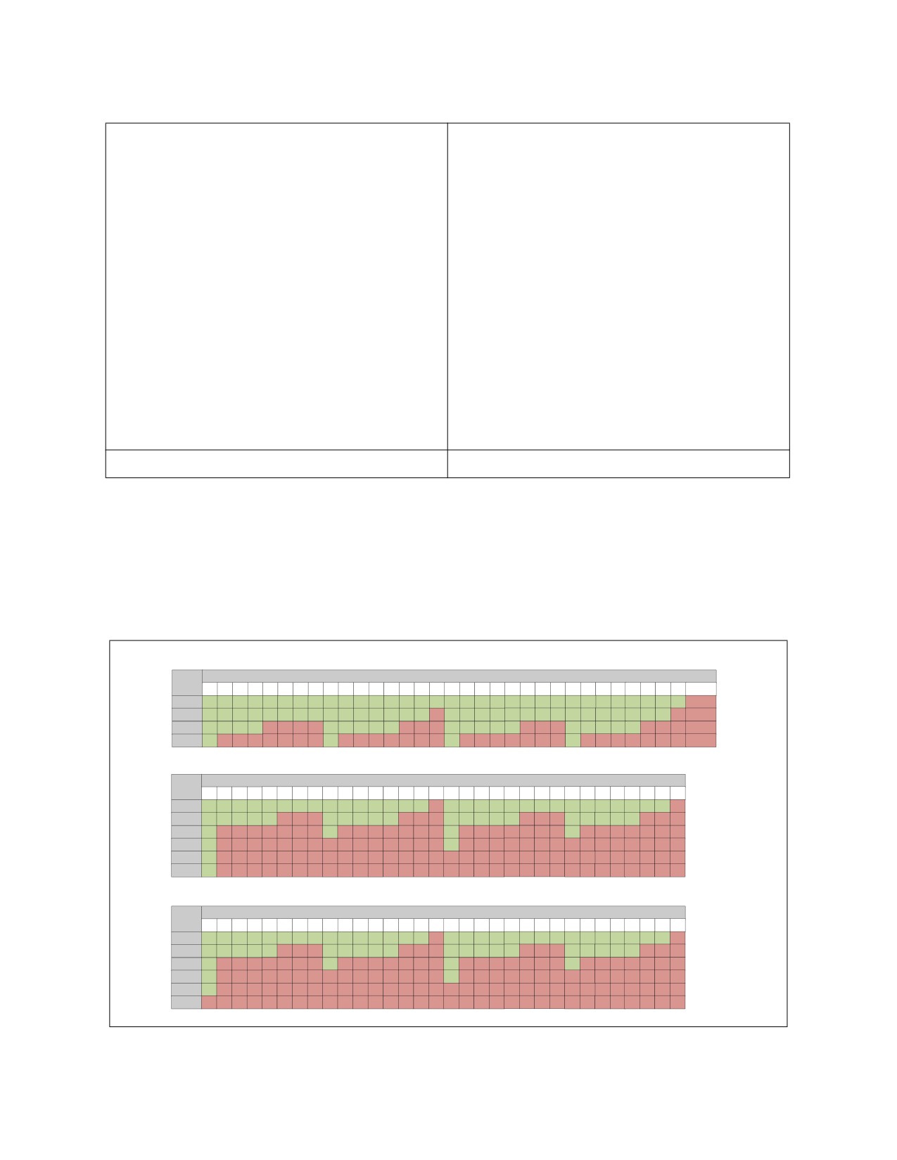
SOFTWARE OPTIMIZATION FOR INTEL® AVX-512 INSTRUCTIONS
Example 18-9. Peeling and Remainder Masking (Contd.)
mainloop:
vmovups zmm1, [rax + rdx]
vfmadd213ps zmm1, zmm3, zmm0
vmovaps [rbx + rdx], zmm1 // aligned store is safe here
!!
add rdx, 0x40
sub r8, 1
jne mainloop
remainder:
// produce mask for remainder
and rcx, 0xF // number of elements in remainder
jz end // no elements in remainder
vpbroadcastd zmm2, ecx
vpcmpd k2, zmm10, zmm2, 1 //compare lower
vmovups zmm1 {k2}{z}, [rax + rdx]
vfmadd213ps zmm1 {k2}{z}, zmm3, zmm0
vmovaps [rbx + rdx] {k2}, zmm1 //aligned
end:
Baseline 1x
Speedup: 1.04x
18.3
FORWARDING AND UNMASKED OPERATIONS
When using an unmasked store instruction, and load instruction after it, data forwarding depends on load
type, size and address offset from store address, and does not depend on the store address itself (i.e.,
the store address does not have to be aligned to or fit into cache line, forwarding will occur for non-
aligned and even line-split stores).
The figure below describes all possible cases when data forwarding will occur.
General Purpose Registers (GPR)
Load
Offset from store address (in bytes)
size
0
1
2
3
4
5
6
7
8
9
10
11
12
13
14
15
16
17
18
19
20
21
22
23
24
25
26
27
28
29
30
31
32..63
1
Y
Y
Y
Y
Y
Y
Y
Y
Y
Y
Y
Y
Y
Y
Y
Y
Y
Y
Y
Y
Y
Y
Y
Y
Y
Y
Y
Y
Y
Y
Y
Y
N
2
Y
Y
Y
Y
Y
Y
Y
Y
Y
Y
Y
Y
Y
Y
Y
N
Y
Y
Y
Y
Y
Y
Y
Y
Y
Y
Y
Y
Y
Y
Y
N
N
4
Y
Y
Y
Y
N
N
N
N
Y
Y
Y
Y
Y
N
N
N
Y
Y
Y
Y
Y
N
N
N
Y
Y
Y
Y
Y
N
N
N
N
8
Y
N
N
N
N
N
N
N
Y
N
N
N
N
N
N
N
Y
N
N
N
N
N
N
N
Y
N
N
N
N
N
N
N
N
X87, MMX, XMM, YMM, ZMM
Load
Offset from store address (in bytes)
size
0
1
2
3
4
5
6
7
8
9
10
11
12
13
14
15
16
17
18
19
20
21
22
23
24
25
26
27
28
29
30
31
2
Y
Y
Y
Y
Y
Y
Y
Y
Y
Y
Y
Y
Y
Y
Y
N
Y
Y
Y
Y
Y
Y
Y
Y
Y
Y
Y
Y
Y
Y
Y
N
4
Y
Y
Y
Y
Y
N
N
N
Y
Y
Y
Y
Y
N
N
N
Y
Y
Y
Y
Y
N
N
N
Y
Y
Y
Y
Y
N
N
N
8
Y
N
N
N
N
N
N
N
Y
N
N
N
N
N
N
N
Y
N
N
N
N
N
N
N
Y
N
N
N
N
N
N
N
16
Y
N
N
N
N
N
N
N
N
N
N
N
N
N
N
N
Y
N
N
N
N
N
N
N
N
N
N
N
N
N
N
N
32
Y
N
N
N
N
N
N
N
N
N
N
N
N
N
N
N
N
N
N
N
N
N
N
N
N
N
N
N
N
N
N
N
64
Y
N
N
N
N
N
N
N
N
N
N
N
N
N
N
N
N
N
N
N
N
N
N
N
N
N
N
N
N
N
N
N
X87, MMX, XMM, YMM, ZMM
Load
Offset from store address (in bytes)
size
32
33
34
35
36
37
38
39
40
41
42
43
44
45
46
47
48
49
50
51
52
53
54
55
56
57
58
59
60
61
62
63
2
Y
Y
Y
Y
Y
Y
Y
Y
Y
Y
Y
Y
Y
Y
Y
N
Y
Y
Y
Y
Y
Y
Y
Y
Y
Y
Y
Y
Y
Y
Y
N
4
Y
Y
Y
Y
Y
N
N
N
Y
Y
Y
Y
Y
N
N
N
Y
Y
Y
Y
Y
N
N
N
Y
Y
Y Y
Y
N
N
N
8
Y
N N N N N N N Y
N N N N N N N Y
N N N N N N N Y
N N N
N
N
N
N
16
Y
N N N N N N N N N N N N N N N Y
N N N N N N N N N N N
N
N
N
N
32
Y
N N N N N N N N N N N N N N N N N N N N N N N N N N N
N
N
N
N
64
N N N N N N N N N N N N N N N N N N N N N N N N N N N N
N
N
N
N
S OM 00 00 6
Figure 18-3. Data Forwarding Cases
18-16
SOFTWARE OPTIMIZATION FOR INTEL® AVX-512 INSTRUCTIONS
There are two important points to be considered when using data forwarding.
1. Data forwarding to GPR is possible only from the lower 256 bits of store instruction. Note this when
loading GPR with data that has recently been written.
2. Do not use masks, as forwarding is supported only for certain masks.
18.4
FORWARDING AND MEMORY MASKING
When using masked store and load, consider the following:
• When the mask is not all-ones or all-zeroes, the load operation, following the masked store operation
from the same address is blocked, until the data is written to the cache.
• Unlike GPR forwarding rules, vector loads whether or not they are masked, do not forward unless
load and store addresses are exactly the same.
— st_mask = 10101010, ld_mask = 01010101, can forward: no, should block: yes
— st_mask = 00001111, ld_mask = 00000011, can forward: no, should block: yes
• When the mask is all-ones, blocking does not occur, because the data may be forwarded to the load
operation.
— st_mask = 11111111, ld_mask = don’t care, can forward: yes, should block: no
• When mask is all-zeroes, blocking does not occur, though neither does forwarding.
— st_mask = 00000000, ld_mask = don’t care, can forward: no, should block: no
In summary, a masked store should be used carefully, for example, if the remainder size is known at
compile time to be 1, and there is a load operation from the same cache line after it (or there is an
overlap in addresses + vector lengths), it may be better to use scalar remainder processing, rather than
a masked remainder block.
18.5
DATA COMPRESS
The data compress operation reads elements from an input buffer on indices specified by mask register
1's bits. The elements which have been read, are then written to the destination buffer. If the number of
elements is less than the destination register size, the rest of the space is filled with zeroes.
The following figure describes the data compress operation.
if (k[i] == 1)
{
dest[a] = src[i];
a++;
}
18-17
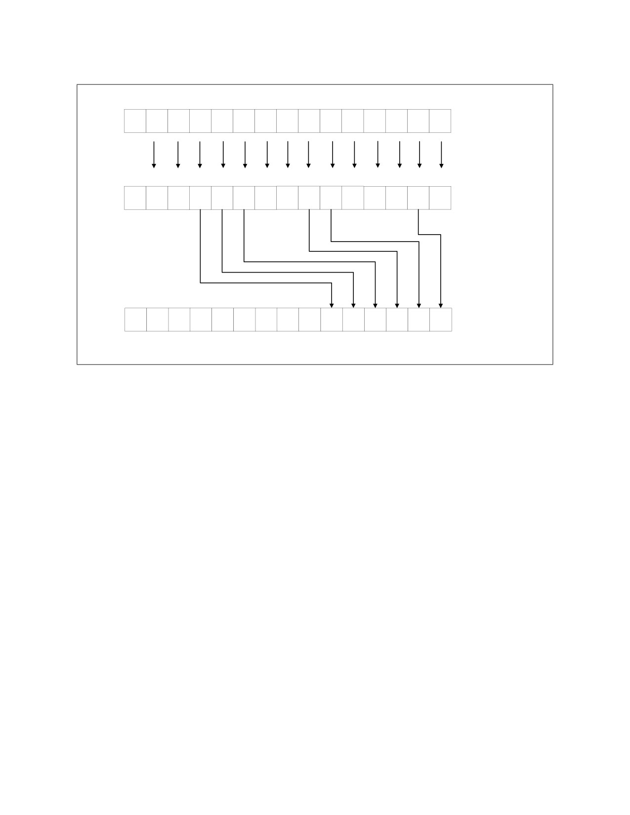
SOFTWARE OPTIMIZATION FOR INTEL® AVX-512 INSTRUCTIONS
…
5
4
3
2
1
0
bits
Mask
0
0
1
1
1
0
0
1
1
0
0
0
1
0
Register
… 63 32 31
0 bits
Input
a13
a12
a11
a10
a9
a8
a7
a6
a5
a4
a3
a2
a1
a0
Buffer
… 63
32 31
0 bits
0
0
0
0
0
0
0
0
a11
a10
a9
a6
a5
a1
Destination
SOM00007
Figure 18-4. Data Compress Operation
18.5.1 Data Compress Example
The following snippet shows collection of all positive elements from one array to another array.
for (int i=0; i<SIZE; i++)
{
if ( a[i] > 0 )
b[j++] = a[i];
}
18-18

SOFTWARE OPTIMIZATION FOR INTEL® AVX-512 INSTRUCTIONS
Following are four implementations for the compress operation from an array of dword elements.
• Alternative 1 uses scalar data access and checks each element separately. If it is greater than 0 it is
written to the destination array.
• Alternative 2 is Intel AVX code that uses a shuffle instruction together with the pre-allocated and pre-
initialized table with shuffle keys. The compare instruction provides the entry point number to the
shuffle-key table. Then the key is loaded and the original array is shuffled according to the keys. Four
elements are processed in each iteration.
• Alternative 3 uses the same algorithm as in Alternative 2, but uses Intel AVX2 256-bit registers, and
a permutation on the dword instruction instead of using byte shuffle. Eight elements are processed in
each iteration.
• Alternative 4 is an Intel AVX-512 algorithm, which uses the vpcompress instruction together with the
mask register as a compress key. 16 elements are processed in each iteration.
Example 18-10. Comparing Intel® AVX-512 Data Compress with Other Alternatives
Alternative 1: Scalar
mov rsi, source
mov rdi, dest
mov r9, len
xor r8, r8
xor r10, r10
mainloop:
mov r11d, dword ptr [rsi+r8*4]
test r11d, r11d
jle m1
mov dword ptr [rdi+r10*4], r11d
inc r10
m1:
inc r8
cmp r8, r9
jne mainloop
Baseline 1x
18-19

SOFTWARE OPTIMIZATION FOR INTEL® AVX-512 INSTRUCTIONS
Example 18-10. Comparing Intel® AVX-512 Data Compress with Other Alternatives (Contd.)
Alternative 2: Intel® AVX
mov rsi, source
mov rdi, dest
mov r14, shuffle_LUT
mov r15, write_mask
mov r9, len
xor r8, r8
xor r11, r11
vpxor xmm0, xmm0, xmm0
mainloop:
vmovdqa xmm1, [rsi+r8*4]
vpcmpgtd xmm2, xmm1, xmm0
mov r10, 4
vmovmskps r13, xmm2
shl r13, 4
vmovdqu xmm3, [r14+r13]
vpshufb xmm2, xmm1, xmm3
popcnt r13, r13
sub r10, r13
vmovdqu xmm3, [r15+r10*4]
vmaskmovps [rdi+r11*4], xmm3, xmm2
add r11, r13
add r8, 4
cmp r8, r9
jne mainloop
shuffle_LUT:
.int 0x80808080, 0x80808080, 0x80808080, 0x80808080
.int 0x03020100, 0x80808080, 0x80808080, 0x80808080
.int 0x07060504, 0x80808080, 0x80808080, 0x80808080
.int 0x03020100, 0x07060504, 0x80808080, 0x80808080
.int 0x0b0A0908, 0x80808080, 0x80808080, 0x80808080
.int 0x03020100, 0x0b0A0908, 0x80808080, 0x80808080
.int 0x07060504, 0x0b0A0908, 0x80808080, 0x80808080
.int 0x03020100, 0x07060504, 0x0b0A0908, 0x80808080
.int 0x0F0E0D0C, 0x80808080, 0x80808080, 0x80808080
.int 0x03020100, 0x0F0E0D0C, 0x80808080, 0x80808080
.int 0x07060504, 0x0F0E0D0C, 0x80808080, 0x80808080
.int 0x03020100, 0x07060504, 0x0F0E0D0C, 0x80808080
.int 0x0b0A0908, 0x0F0E0D0C, 0x80808080, 0x80808080
.int 0x03020100, 0x0b0A0908, 0x0F0E0D0C, 0x80808080
.int 0x07060504, 0x0b0A0908, 0x0F0E0D0C, 0x80808080
.int 0x03020100, 0x07060504, 0x0b0A0908, 0x0F0E0D0C
write_mask:
.int 0x80000000, 0x80000000, 0x80000000, 0x80000000
.int 0x00000000, 0x00000000, 0x00000000, 0x00000000
Speedup: 2.87x
18-20

SOFTWARE OPTIMIZATION FOR INTEL® AVX-512 INSTRUCTIONS
Example 18-10. Comparing Intel® AVX-512 Data Compress with Other Alternatives (Contd.)
Alternative 3: Intel® AVX2
mov rsi, source
mov rdi, dest
mov r14, shuffle_LUT
mov r15, write_mask
mov r9, len
xor r8, r8
xor r11, r11
vpxor ymm0, ymm0, ymm0
mainloop:
vmovdqa ymm1, [rsi+r8*4]
vpcmpgtd ymm2, ymm1, ymm0
mov r10, 8
vmovmskps r13, ymm2
shl r13, 5
vmovdqu ymm3, [r14+r13]
vpermd ymm2, ymm3, ymm1
popcnt r13, r13
sub r10, r13
vmovdqu ymm3, [r15+r10*4]
vmaskmovps [rdi+r11*4], ymm3, ymm2
add r11, r13
add r8, 8
cmp r8, r9
jne mainloop
// The lookup table is too large to reproduce in the document. It consists of 256 rows of 8 32 bit integers.
//The first 8 and the last 8 rows are shown below.
shuffle_LUT:
.int 0x0, 0x0, 0x0, 0x0, 0x0, 0x0, 0x0, 0x0
.int 0x0, 0x0, 0x0, 0x0, 0x0, 0x0, 0x0, 0x0
.int 0x1, 0x0, 0x0, 0x0, 0x0, 0x0, 0x0, 0x0
.int 0x0, 0x1, 0x0, 0x0, 0x0, 0x0, 0x0, 0x0
.int 0x2, 0x0, 0x0, 0x0, 0x0, 0x0, 0x0, 0x0
.int 0x0, 0x2, 0x0, 0x0, 0x0, 0x0, 0x0, 0x0
.int 0x1, 0x2, 0x0, 0x0, 0x0, 0x0, 0x0, 0x0
.int 0x0, 0x1, 0x2, 0x0, 0x0, 0x0, 0x0, 0x0
// Skipping 240 lines
.int 0x3, 0x4, 0x5, 0x6, 0x7, 0x0, 0x0, 0x0
.int 0x0, 0x3, 0x4, 0x5, 0x6, 0x7, 0x0, 0x0
.int 0x1, 0x3, 0x4, 0x5, 0x6, 0x7, 0x0, 0x0
.int 0x0, 0x1, 0x3, 0x4, 0x5, 0x6, 0x7, 0x0
.int 0x2, 0x3, 0x4, 0x5, 0x6, 0x7, 0x0, 0x0
.int 0x0, 0x2, 0x3, 0x4, 0x5, 0x6, 0x7, 0x0
.int 0x1, 0x2, 0x3, 0x4, 0x5, 0x6, 0x7, 0x0
.int 0x0, 0x1, 0x2, 0x3, 0x4, 0x5, 0x6, 0x7
18-21

SOFTWARE OPTIMIZATION FOR INTEL® AVX-512 INSTRUCTIONS
Example 18-10. Comparing Intel® AVX-512 Data Compress with Other Alternatives (Contd.)
write_mask:
.int 0x80000000, 0x80000000, 0x80000000, 0x80000000
.int 0x80000000, 0x80000000, 0x80000000, 0x80000000
.int 0x00000000, 0x00000000, 0x00000000, 0x00000000
.int 0x00000000, 0x00000000, 0x00000000, 0x00000000
Speedup: 5.27x
Alternative 4: Intel® AVX-512
mov rsi, source
mov rdi, dest
mov r9, len
xor r8, r8
xor r10, r10
vpxord zmm0, zmm0, zmm0
mainloop:
vmovdqa32 zmm1, [rsi+r8*4]
vpcmpgtd k1, zmm1, zmm0
vpcompressd zmm2 {k1}, zmm1
vmovdqu32 [rdi+r10*4], zmm2
kmovd r11d, k1
popcnt r12, r11
add r8, 16
add r10, r12
cmp r8, r9
jne mainloop
Speedup: 11.9x
18.6
DATA EXPAND
Data expand operations read elements from the source array (register) and put them in the destination
register in the places indicated by enabled bits in the mask register. If the number of enabled bits is less
than destination register size, the extra values are ignored.
if (k[i] == 1)
{
dest[i] = src[a];
a++;
}
18-22
SOFTWARE OPTIMIZATION FOR INTEL® AVX-512 INSTRUCTIONS
… 63 32 31
0 bits
Input
a13
a12
a11
a10
a9
a8
a7
a6
a5
a4
a3
a2
a1
a0
Buffer
…
13
12
11
10
9
8
7
6
5
4
3
2
1
0
bits
Mask
0
0
1
1
1
0
0
1
1
0
0
0
1
0
Register
… 63
32 31
0 bits
0
0
a5
a4
a3
0
0
a2
a1
0
0
0
a0
0
Destination
SOM00008
Figure 18-5. Data Expand Operation
18.6.1 Data Expand Example
The following snippet shows an example of using the expand operation. For every positive number in an
array, the code sets its consecutive number among positives.
for (int i=0; i<SIZE; i++)
{
if (a[i] > 0)
dest[i] = a[count++];
else
dest[i] = 0;
}
Here are three implementations for the expand operation from an array of 16 dword elements.
• Alternative 1 uses scalar data access and checks each element separately. If it is greater than 0 then
the corresponding element in the destination array is rewritten with the value from source value at
index count, and the counter is incremented.
• Alternative 2 shows Intel AVX2 code that uses a shuffle instruction together with the pre-allocated
and pre-initialized table with shuffle keys. The compare instruction provides the entry point number
to the shuffle-key table. Then the key is loaded and the original array is shuffled according to the
keys. Four elements are processed in each iteration.
• Alternative 3 shows Intel AVX-512 code, which uses the vpexpandd instruction together with the
mask register as an expand key. 16 elements are processed in each iteration.
18-23

SOFTWARE OPTIMIZATION FOR INTEL® AVX-512 INSTRUCTIONS
Example 18-11. Comparing Intel® AVX-512 Data Expand Operation with Other Alternatives
Alternative 1: Scalar
Alternative 2: Intel® AVX2 Code
Alternative 3: Intel® AVX-512 Code
mov rsi, input
mov rsi, input
vpxord zmm0, zmm0, zmm0
mov rdi, output
mov rdi, output
mainloop:
mov r9, len
mov r9, len
vmovdqa32 zmm1, [rsi+r8*4]
xor r8, r8
xor r8, r8
vpcmpgtd k1, zmm1, zmm0
xor r10, r10
xor r10, r10
vmovdqu32 zmm1,
mainloop:
vpxor ymm0, ymm0, ymm0
[rsi+r10*4]
mov r11d, dword ptr
mov r14, shuf2
vpexpandd zmm2 {k1}{z},
[rsi+r8*4]
mainloop:
zmm1
test r11d, r11d
vmovdqa ymm1, [rsi+r8*4]
vmovdqu32 [rdi+r8*4], zmm2
jle m1
vpxor ymm4, ymm4, ymm4
add r8, 16
mov r11d, dword ptr
vpcmpgtd ymm2, ymm1, ymm0
kmovd r11d, k1
[rsi+r10*4]
vmovdqu ymm1, [rsi+r10*4]
popcnt r12, r11
mov dword ptr [rdi+r8*4],
vmovmskps r13, ymm2
add r10, r12
r11d
cmp r8, r9
shl r13, 5
inc r10
jne mainloop
vmovdqa ymm3, [r14+r13]
m1:
vpermd ymm4, ymm3, ymm1
inc r8
popcnt r13, r13
cmp r8, r9
add r10, r13
jne mainloop
vmaskmovps [rdi+r8*4], ymm2,
ymm4
add r8, 8
cmp r8, r9
jne mainloop
// The lookup table is too large to
// reproduce in the document. It consists
// of 256 rows of 8 32-bit integers. The
// first 8 and the last 8 rows are shown
// below. The table needs to be 32-byte
// aligned.
shuf2:
.int 0, 0, 0, 0, 0, 0, 0, 0
.int 0, 0, 0, 0, 0, 0, 0, 0
.int 0, 0, 0, 0, 0, 0, 0, 0
.int 0, 1, 0, 0, 0, 0, 0, 0
.int 0, 0, 0, 0, 0, 0, 0, 0
.int 0, 0, 1, 0, 0, 0, 0, 0
.int 0, 0, 1, 0, 0, 0, 0, 0
.int 0, 1, 2, 0, 0, 0, 0, 0
// Skipping 240 lines
.int 0, 0, 0, 0, 1, 2, 3, 4
.int 0, 0, 0, 1, 2, 3, 4, 5
.int 0, 0, 0, 1, 2, 3, 4, 5
.int 0, 1, 0, 2, 3, 4, 5, 6
.int 0, 0, 0, 1, 2, 3, 4, 5
.int 0, 0, 1, 2, 3, 4, 5, 6
.int 0, 0, 1, 2, 3, 4, 5, 6
.int 0, 1, 2, 3, 4, 5, 6, 7
Baseline 1x
Speedup: 4.23x
Speedup: 8.58x
18-24
SOFTWARE OPTIMIZATION FOR INTEL® AVX-512 INSTRUCTIONS
18.7
TERNARY LOGIC
A ternary logic vpternlog operation executes any bitwise logical function between three operands in one
instruction. The instruction requires three operands and an immediate value, which is the truth table of
this logical expression. The first operand is used as destination, and, therefore, destroyed after the
execution.
18.7.1 Ternary Logic Example 1
The following example shows a bitwise logic function of three variables. The function in this example is
defined by the following truth table.
X
1
1
1
1
0
0
0
0
Immediate value
Y
1
1
0
0
1
1
0
0
that is used.
Z
1
0
1
0
1
0
1
0
f(X, Y, Z)
1
0
0
1
0
0
1
0
0x92
SOM00009
Figure 18-6. Ternary Logic Example 1 Truth Table
Using Karnaugh maps on this truth table, we can define the function as:
f(X,Y,Z) =
or, in shorter notation, using fewer binary operations:
f(X,Y,Z) =
The C code for the function above is as follows:
for (int i=0; i<SIZE; i++)
{
Dst[i] = ((~Src2[i]) & (Src1[i] ^ Src3[i])) | (Src1[i] & Src2[i] & Src3[i]);
}
The value of the function for each combination of X, Y and Z gives an immediate value that is used in the
instruction.
Here are three implementations for this logical function applied to all values in X, Y and Z arrays.
• Alternative 1 is an Intel AVX2 256-bit vector computation, using bitwise logical functions available in
Intel AVX2.
• Alternative 2 is a 512-bit vector computation, using bitwise logical functions available in Intel AVX-
512, without using the vpternlog instruction.
• Alternative 3 is an Intel AVX-512 512-bit vector computation, using the vpternlog instruction.
All alternatives in the table are unrolled by factor 2.
18-25

SOFTWARE OPTIMIZATION FOR INTEL® AVX-512 INSTRUCTIONS
Example 18-12. Comparing Ternary Logic to Other Alternatives
Alternative 1: Intel® AVX2
mov rax, src1
mov rbx, src2
mov rcx, src3
mov r11, dst
mov r8, len
xor r10, r10
mainloop:
vmovdqu ymm1, ymmword ptr [rax+r10*4]
vmovdqu ymm3, ymmword ptr [rdx+r10*4]
vmovdqu ymm2, ymmword ptr [rcx+r10*4]
vmovdqu ymm10, ymmword ptr [rcx+r10*4+0x20]
vpand ymm0, ymm1, ymm3
vpxor ymm4, ymm1, ymm2
vpand ymm5, ymm0, ymm2
vpandn ymm6, ymm3, ymm4
vpor ymm7, ymm5, ymm6
vmovdqu ymmword ptr [r11+r10*4], ymm7
vmovdqu ymm9, ymmword ptr [rax+r10*4+0x20]
vmovdqu ymm11, ymmword ptr [rdx+r10*4+0x20]
vpxor ymm12, ymm9, ymm10
vpand ymm8, ymm9, ymm11
vpandn ymm14, ymm11, ymm12
vpand ymm13, ymm8, ymm10
vpor ymm15, ymm13, ymm14
vmovdqu ymmword ptr [r11+r10*4+0x20], ymm15
add r10, 0x10
cmp r10, r8
jb mainloop
Baseline 1x
18-26

SOFTWARE OPTIMIZATION FOR INTEL® AVX-512 INSTRUCTIONS
Example 18-12. Comparing Ternary Logic to Other Alternatives (Contd.)
Alternative 2: Intel® AVX-512 Logic Instructions
Alternative 3: Intel® AVX-512 using vpternlog
Instruction
mov rdi, src1
mov r9, src1
mov rsi, src2
mov r8, src2
mov rdx, src3
mov r10, src3
mov r11, dst
mov r11, dst
mov r8, len
mov rsi, len
xor r10, r10
xor rax rax
mainloop:
mainloop:
vmovups zmm2, zmmword ptr [rdi+r10*4]
vmovaps zmm1, [r8+rax*4]
vmovups zmm4, zmmword ptr [rdi+r10*4+0x40]
vmovaps zmm0, [r9+rax*4]
vmovups zmm6, zmmword ptr [rsi+r10*4]
vpternlogd zmm0,zmm1,[r10], 0x92
vmovups zmm8, zmmword ptr [rsi+r10*4+0x40]
vmovaps [r11], zmm0
vmovups zmm3, zmmword ptr [rdx+r10*4]
vmovaps zmm1, [r8+rax*4+0x40]
vmovups zmm5, zmmword ptr [rdx+r10*4+0x40]
vmovaps zmm0, [r9+rax*4+0x40]
vpandd zmm0, zmm2, zmm6
vpternlogd zmm0,zmm1, [r10+0x40], 0x92
vpandd zmm1, zmm4, zmm8
vmovaps [r11+0x40], zmm0
vpxord zmm7, zmm2, zmm3
add rax, 32
vpxord zmm9, zmm4, zmm5
add r10, 0x80
vpandd zmm10, zmm0, zmm3
add r11, 0x80
vpandd zmm12, zmm1, zmm5
cmp rax, rsi
vpandnd zmm11, zmm6, zmm7
jne mainloop
vpandnd zmm13, zmm8, zmm9
vpord zmm14, zmm10, zmm11
vpord zmm15, zmm12, zmm13
vmovups zmmword ptr [r11+r10*4], zmm14
vmovups zmmword ptr [r11+r10*4+0x40], zmm15
add r10, 0x20
cmp r10, r9
jb mainloop
Speedup: 1.94x
Speedup: 2.36x
(1.22x vs Intel® AVX-512 with logic instructions)
18.7.2 Ternary Logic Example 2
The next example is a sign change operation, frequently used in Fortran. Consider the following code,
running on two arrays of floating point numbers.
for (int i=0; i<SIZE; i++)
{
b[i] = a[i] > 0 ? b[i] : -b[i];
}
18-27
SOFTWARE OPTIMIZATION FOR INTEL® AVX-512 INSTRUCTIONS
This code is equivalent to:
for (int i=0; i<SIZE; i++)
{
b[i] = ( a[i] & 0x80000000 ) ^ b[i];
}
Or, in other words:
This logic expression gives the following truth table.
X
1
1
1
1
0
0
0
0
Immediate value
that is used in the
Y
1
1
0
0
1
1
0
0
vpternlog instruction.
Z
1
0
1
0
1
0
1
0
f(X, Y, Z)
0
1
1
1
1
0
0
0
0x78
SOM00010
Figure 18-7. Ternary Logic Example 2 Truth Table
Therefore one vpternlog instruction can be used instead of using two logic instructions (vpand and
vpxor):
vpternlog x,y,z,0x78
18.8
NEW SHUFFLE INSTRUCTIONS
Intel AVX-512 added 3 new shuffle operations.
• vpermw: a new single source any-to-any word permute.
• permt2[w/d/q/ps/pd]: a new any to any 2 source permute (overriding src register).
• permi2[w/d/q/ps/pd]: a new any to any 2 source permute (overriding control register).
The following figure shows how vpermi2ps is used. Notice that in the following example zmm0 is the
shuffle control but also the output register (the control register is overridden).
vpermi2ps zmm0, zmm1, zmm2
18-28