Intel 64 and IA-32 Architectures. Software Developer’s Manual (Collection, 2023) - page 143

MULTICORE AND INTEL® HYPER-THREADING TECHNOLOGY (INTEL® HT)
Table 11-1. Properties of Synchronization Objects
Operating System
Light Weight User
Synchronization Object
Characteristics
Synchronization Objects
Synchronization
based on MONITOR/MWAIT
Cycles to acquire and
Thousands or Tens of thousands
release (if there is a
Hundreds of cycles
Hundreds of cycles
cycles
contention)
Saves power by halting the core or
Some power saving if using
Saves more power than
Power consumption
logical processor if idle
PAUSE
PAUSE
Returns to the OS scheduler if
Scheduling and
Does not return to OS
Does not return to OS
contention exists (can be tuned
context switching
scheduler voluntarily
scheduler voluntarily
with earlier spin loop count)
Ring level
Ring 0
Ring 3
Ring 0
Must lock accesses to
synchronization variable if
Same as light weight.
Some objects provide intra-process
several threads may write
Can be used only on
Miscellaneous
synchronization and some are for
to it simultaneously.
systems supporting
inter-process communication
Otherwise can write
MONITOR/MWAIT
without locks.
• Number of active threads
• Number of active threads is
is less than or equal to
greater than number of cores
• Same as light weight
Recommended use
number of cores
• Waiting thousands of cycles for a
objects
conditions
• Infrequent contention
signal
• MONITOR/MWAIT available
• Need inter process
• Synchronization among processes
synchronization
11.4.2 Synchronization for Short Periods
The frequency and duration that a thread needs to synchronize with other threads depends application
characteristics. When a synchronization loop needs very fast response, applications may use a spin-wait
loop.
A spin-wait loop is typically used when one thread needs to wait a short amount of time for another
thread to reach a point of synchronization. A spin-wait loop consists of a loop that compares a synchro-
nization variable with some predefined value. See Example 11-4(a).
On a modern microprocessor with a superscalar speculative execution engine, a loop like this results in
the issue of multiple simultaneous read requests from the spinning thread. These requests usually
execute out-of-order with each read request being allocated a buffer resource. On detection of a write by
a worker thread to a load that is in progress, the processor must guarantee no violations of memory
order occur. The necessity of maintaining the order of outstanding memory operations inevitably costs
the processor a severe penalty that impacts all threads.
This penalty occurs on the Pentium M processor, the Intel Core Solo and Intel Core Duo processors.
However, the penalty on these processors is small compared with penalties suffered on the Pentium 4
and Intel Xeon processors. There the performance penalty for exiting the loop is about 25 times more
severe.
On a processor supporting HT Technology, spin-wait loops can consume a significant portion of the
execution bandwidth of the processor. One logical processor executing a spin-wait loop can severely
impact the performance of the other logical processor.
11-11

MULTICORE AND INTEL® HYPER-THREADING TECHNOLOGY (INTEL® HT)
Example 11-4. Spin-wait Loop and PAUSE Instructions
(a) An un-optimized spin-wait loop experiences performance penalty when exiting the loop. It consumes execution
resources without contributing computational work.
do {
// This loop can run faster than the speed of memory access,
// other worker threads cannot finish modifying sync_var until
// outstanding loads from the spinning loops are resolved.
} while( sync_var != constant_value);
(b) Inserting the PAUSE instruction in a fast spin-wait loop prevents performance-penalty to the spinning thread and the
worker thread
do {
_asm pause
// Ensure this loop is de-pipelined, i.e. preventing more than one
// load request to sync_var to be outstanding,
// avoiding performance penalty when the worker thread updates
// sync_var and the spinning thread exiting the loop.
}
while( sync_var != constant_value);
(c) A spin-wait loop using a “test, test-and-set” technique to determine the availability of the synchronization variable.
This technique is recommended when writing spin-wait loops to run on Intel 64 and IA-32 architecture processors.
Spin_Lock:
CMP lockvar, 0 ;
// Check if lock is free.
JE Get_lock
PAUSE;
// Short delay.
JMP Spin_Lock;
Get_Lock:
MOV EAX, 1;
XCHG EAX, lockvar;
// Try to get lock.
CMP EAX, 0;
// Test if successful.
JNE Spin_Lock;
Critical_Section:
<critical section code>
MOV lockvar, 0;
// Release lock.
User/Source Coding Rule 13. (M impact, H generality) Insert the PAUSE instruction in fast spin
loops and keep the number of loop repetitions to a minimum to improve overall system performance.
The penalty of exiting from a spin-wait loop can be avoided by inserting a PAUSE instruction in the loop.
In spite of the name, the PAUSE instruction improves performance by introducing a slight delay in the
loop and effectively causing the memory read requests to be issued at a rate that allows immediate
detection of any store to the synchronization variable. This prevents the occurrence of a long delay due
to memory order violation.
One example of inserting the PAUSE instruction in a simplified spin-wait loop is shown in
Example 11-4(b). The PAUSE instruction is compatible with all Intel 64 and IA-32 processors. On IA-32
processors prior to Intel NetBurst microarchitecture, the PAUSE instruction is essentially a NOP instruc-
tion. Additional examples of optimizing spin-wait loops using the PAUSE instruction are available in Appli-
cation note AP-949, Using Spin-Loops on Intel® Pentium® 4 Processor and Intel® Xeon® Processor.
Inserting the PAUSE instruction has the added benefit of significantly reducing the power consumed
during the spin-wait because fewer system resources are used.
11-12

MULTICORE AND INTEL® HYPER-THREADING TECHNOLOGY (INTEL® HT)
11.4.3 Optimization with Spin-Locks
Spin-locks are typically used when several threads needs to modify a synchronization variable and the
synchronization variable must be protected by a lock to prevent unintentional overwrites. When the lock
is released, however, several threads may compete to acquire it at once. Such thread contention signifi-
cantly reduces performance scaling with respect to frequency, number of discrete processors, and HT
Technology.
To reduce the performance penalty, one approach is to reduce the likelihood of many threads competing
to acquire the same lock. Apply a software pipelining technique to handle data that must be shared
between multiple threads.
Instead of allowing multiple threads to compete for a given lock, no more than two threads should have
write access to a given lock. If an application must use spin-locks, include the PAUSE instruction in the
wait loop. Example 11-4(c) shows an example of the “test, test-and-set” technique for determining the
availability of the lock in a spin-wait loop.
User/Source Coding Rule 14. (M impact, L generality) Replace a spin lock that may be acquired
by multiple threads with pipelined locks such that no more than two threads have write accesses to one
lock. If only one thread needs to write to a variable shared by two threads, there is no need to use a
lock.
11.4.4 Synchronization for Longer Periods
When using a spin-wait loop not expected to be released quickly, an application should follow these
guidelines:
• Keep the duration of the spin-wait loop to a minimum number of repetitions.
• Applications should use an OS service to block the waiting thread; this can release the processor so
that other runnable threads can make use of the processor or available execution resources.
On processors supporting HT Technology, operating systems should use the HLT instruction if one logical
processor is active and the other is not. HLT will allow an idle logical processor to transition to a halted
state; this allows the active logical processor to use all the hardware resources in the physical package.
An operating system that does not use this technique must still execute instructions on the idle logical
processor that repeatedly check for work. This “idle loop” consumes execution resources that could
otherwise be used to make progress on the other active logical processor.
If an application thread must remain idle for a long time, the application should use a thread blocking API
or other method to release the idle processor. The techniques discussed here apply to traditional MP
system, but they have an even higher impact on processors that support HT Technology.
Typically, an operating system provides timing services, for example Sleep(dwMilliseconds)1; such vari-
ables can be used to prevent frequent checking of a synchronization variable.
Another technique to synchronize between worker threads and a control loop is to use a thread-blocking
API provided by the OS. Using a thread-blocking API allows the control thread to use less processor
cycles for spinning and waiting. This gives the OS more time quanta to schedule the worker threads on
available processors. Furthermore, using a thread-blocking API also benefits from the system idle loop
optimization that OS implements using the HLT instruction.
User/Source Coding Rule 15. (H impact, M generality) Use a thread-blocking API in a long idle
loop to free up the processor.
Using a spin-wait loop in a traditional MP system may be less of an issue when the number of runnable
threads is less than the number of processors in the system. If the number of threads in an application is
expected to be greater than the number of processors (either one processor or multiple processors), use
a thread-blocking API to free up processor resources. A multithreaded application adopting one control
thread to synchronize multiple worker threads may consider limiting worker threads to the number of
processors in a system and use thread-blocking APIs in the control thread.
1. The Sleep() API is not thread-blocking, because it does not guarantee the processor will be released. Example 11-5(a)
shows an example of using Sleep(0), which does not always realize the processor to another thread.
11-13

MULTICORE AND INTEL® HYPER-THREADING TECHNOLOGY (INTEL® HT)
11.4.4.1 Avoid Coding Pitfalls in Thread Synchronization
Synchronization between multiple threads must be designed and implemented with care to achieve good
performance scaling with respect to the number of discrete processors and the number of logical
processor per physical processor. No single technique is a universal solution for every synchronization
situation.
The pseudo-code example in Example 11-5(a) illustrates a polling loop implementation of a control
thread. If there is only one runnable worker thread, an attempt to call a timing service API, such as
Sleep(0), may be ineffective in minimizing the cost of thread synchronization. Because the control thread
still behaves like a fast spinning loop, the only runnable worker thread must share execution resources
with the spin-wait loop if both are running on the same physical processor that supports HT Technology.
If there are more than one runnable worker threads, then calling a thread blocking API, such as Sleep(0),
could still release the processor running the spin-wait loop, allowing the processor to be used by another
worker thread instead of the spinning loop.
A control thread waiting for the completion of worker threads can usually implement thread synchroniza-
tion using a thread-blocking API or a timing service, if the worker threads require significant time to
complete. Example 11-5(b) shows an example that reduces the overhead of the control thread in its
thread synchronization.
Example 11-5. Coding Pitfall using Spin Wait Loop
(a) A spin-wait loop attempts to release the processor incorrectly. It experiences a performance penalty if the only
worker thread and the control thread runs on the same physical processor package.
// Only one worker thread is running,
// the control loop waits for the worker thread to complete.
ResumeWorkThread(thread_handle);
While (!task_not_done ) {
Sleep(0)
// Returns immediately back to spin loop.
…
}
(b) A polling loop frees up the processor correctly.
// Let a worker thread run and wait for completion.
ResumeWorkThread(thread_handle);
While (!task_not_done ) {
Sleep(FIVE_MILISEC)
// This processor is released for some duration, the processor
// can be used by other threads.
…
}
In general, OS function calls should be used with care when synchronizing threads. When using OS-
supported thread synchronization objects (critical section, mutex, or semaphore), preference should be
given to the OS service that has the least synchronization overhead, such as a critical section.
11.4.5 Prevent Sharing of Modified Data and False-Sharing
Depending on the cache topology relative to processor/core topology and the specific underlying
microarchitecture, sharing of modified data can incur some degree of performance penalty when a soft-
ware thread running on one core tries to read or write data that is currently present in modified state in
the local cache of another core. This will cause eviction of the modified cache line back into memory and
reading it into the first-level cache of the other core. The latency of such cache line transfer is much
higher than using data in the immediate first level cache or second level cache.
11-14

MULTICORE AND INTEL® HYPER-THREADING TECHNOLOGY (INTEL® HT)
False sharing applies to data used by one thread that happens to reside on the same cache line as
different data used by another thread. These situations can also incur a performance delay depending on
the topology of the logical processors/cores in the platform.
False sharing can experience a performance penalty when the threads are running on logical processors
reside on different physical processors or processor cores. For processors that support HT Technology,
false-sharing incurs a performance penalty when two threads run on different cores, different physical
processors, or on two logical processors in the physical processor package. In the first two cases, the
performance penalty is due to cache evictions to maintain cache coherency. In the latter case, perfor-
mance penalty is due to memory order machine clear conditions.
A generic approach for multi-threaded software to prevent incurring false-sharing penalty is to allocate
separate critical data or locks with alignment granularity according to a “false-sharing threshold” size.
The following steps will allow software to determine the “false-sharing threshold” across Intel proces-
sors:
1. If the processor supports CLFLUSH instruction, i.e. CPUID.01H:EDX.CLFLUSH[bit 19] =1:
Use the CLFLUSH line size, i.e. the integer value of CPUID.01H:EBX[15:8], as the “false-sharing
threshold”.
2. If CLFLUSH line size is not available, use CPUID leaf 4 as described below:
Determine the “false-sharing threshold” by evaluating the largest system coherency line size among
valid cache types that are reported via the sub-leaves of CPUID leaf 4. For each sub-leaf n, its
associated system coherency line size is (CPUID.(EAX=4, ECX=n):EBX[11:0] + 1).
3. If neither CLFLUSH line size is available, nor CPUID leaf 4 is available, then software may choose the
“false-sharing threshold” from one of the following:
a. Query the descriptor tables of CPUID leaf 2 and choose from available descriptor entries.
b. A Family/Model-specific mechanism available in the platform or a Family/Model-specific known
value.
c. Default to a safe value 64 bytes.
User/Source Coding Rule 16. (H impact, M generality) Beware of false sharing within a cache line
or within a sector. Allocate critical data or locks separately using alignment granularity not smaller than
the “false-sharing threshold”.
When a common block of parameters is passed from a parent thread to several worker threads, it is
desirable for each work thread to create a private copy (each copy aligned to multiples of the “false-
sharing threshold”) of frequently accessed data in the parameter block.
11.4.6 Placement of Shared Synchronization Variable
On processors based on Intel NetBurst microarchitecture, bus reads typically fetch 128 bytes into a
cache, the optimal spacing to minimize eviction of cached data is 128 bytes. To prevent false-sharing,
synchronization variables and system objects (such as a critical section) should be allocated to reside
alone in a 128-byte region and aligned to a 128-byte boundary.
Example 11-6 shows a way to minimize the bus traffic required to maintain cache coherency in MP
systems. This technique is also applicable to MP systems using processors with or without HT Technology.
Example 11-6. Placement of Synchronization and Regular Variables
int regVar;
int padding[32];
int SynVar[32*NUM_SYNC_VARS];
int AnotherVar;
11-15

MULTICORE AND INTEL® HYPER-THREADING TECHNOLOGY (INTEL® HT)
On Pentium M, Intel Core Solo, Intel Core Duo processors, and processors based on Intel Core microar-
chitecture; a synchronization variable should be placed alone and in separate cache line to avoid false-
sharing. Software must not allow a synchronization variable to span across page boundary.
User/Source Coding Rule 17. (M impact, ML generality) Place each synchronization variable
alone, separated by 128 bytes or in a separate cache line.
User/Source Coding Rule 18. (H impact, L generality) Do not place any spin lock variable to span
a cache line boundary.
At the code level, false sharing is a special concern in the following cases:
• Global data variables and static data variables that are placed in the same cache line and are written
by different threads.
• Objects allocated dynamically by different threads may share cache lines. Make sure that the
variables used locally by one thread are allocated in a manner to prevent sharing the cache line with
other threads.
Another technique to enforce alignment of synchronization variables and to avoid a cacheline being
shared is to use compiler directives when declaring data structures. See Example 11-7.
Example 11-7. Declaring Synchronization Variables without Sharing a Cache Line
__declspec(align(64)) unsigned __int64 sum;
struct sync_struct {…};
__declspec(align(64)) struct sync_struct sync_var;
Other techniques that prevent false-sharing include:
• Organize variables of different types in data structures (because the layout that compilers give to
data variables might be different than their placement in the source code).
• When each thread needs to use its own copy of a set of variables, declare the variables with:
— Directive threadprivate, when using OpenMP.
— Modifier __declspec (thread), when using Microsoft compiler.
• In managed environments that provide automatic object allocation, the object allocators and
garbage collectors are responsible for layout of the objects in memory so that false sharing through
two objects does not happen.
• Provide classes such that only one thread writes to each object field and close object fields, in order
to avoid false sharing.
One should not equate the recommendations discussed in this section as favoring a sparsely populated
data layout. The data-layout recommendations should be adopted when necessary and avoid unneces-
sary bloat in the size of the work set.
11.5
SYSTEM BUS OPTIMIZATION
The system bus services requests from bus agents (e.g. logical processors) to fetch data or code from
the memory sub-system. The performance impact due data traffic fetched from memory depends on the
characteristics of the workload, and the degree of software optimization on memory access, locality
enhancements implemented in the software code. A number of techniques to characterize memory traffic
of a workload is discussed in Appendix A. Optimization guidelines on locality enhancement is also
discussed in Section 3.6.10, “Locality Enhancement,” and Section 9.5.11, “Hardware Prefetching and
Cache Blocking Techniques.”
The techniques described in Chapter 3 and Chapter 9 benefit application performance in a platform
where the bus system is servicing a single-threaded environment. In a multi-threaded environment, the
bus system typically services many more logical processors, each of which can issue bus requests inde-
11-16
MULTICORE AND INTEL® HYPER-THREADING TECHNOLOGY (INTEL® HT)
pendently. Thus, techniques on locality enhancements, conserving bus bandwidth, reducing large-stride-
cache-miss-delay can have strong impact on processor scaling performance.
11.5.1 Conserve Bus Bandwidth
In a multithreading environment, bus bandwidth may be shared by memory traffic originated from
multiple bus agents (These agents can be several logical processors and/or several processor cores).
Preserving the bus bandwidth can improve processor scaling performance. Also, effective bus bandwidth
typically will decrease if there are significant large-stride cache-misses. Reducing the amount of large-
stride cache misses (or reducing DTLB misses) will alleviate the problem of bandwidth reduction due to
large-stride cache misses.
One way for conserving available bus command bandwidth is to improve the locality of code and data.
Improving the locality of data reduces the number of cache line evictions and requests to fetch data. This
technique also reduces the number of instruction fetches from system memory.
User/Source Coding Rule 19. (M impact, H generality) Improve data and code locality to
conserve bus command bandwidth.
Using a compiler that supports profiler-guided optimization can improve code locality by keeping
frequently used code paths in the cache. This reduces instruction fetches. Loop blocking can also improve
the data locality. Other locality enhancement techniques can also be applied in a multithreading environ-
ment to conserve bus bandwidth (see Section 9.5, “Memory Optimization Using Prefetch”).
Because the system bus is shared between many bus agents (logical processors or processor cores),
software tuning should recognize symptoms of the bus approaching saturation. One useful technique is
to examine the queue depth of bus read traffic. When the bus queue depth is high, locality enhancement
to improve cache utilization will benefit performance more than other techniques, such as inserting more
software prefetches or masking memory latency with overlapping bus reads. An approximate working
guideline for software to operate below bus saturation is to check if bus read queue depth is significantly
below 5.
Some MP and workstation platforms may have a chipset that provides two system buses, with each bus
servicing one or more physical processors. The guidelines for conserving bus bandwidth described above
also applies to each bus domain.
11.5.2 Understand the Bus and Cache Interactions
Be careful when parallelizing code sections with data sets that results in the total working set exceeding
the second-level cache and /or consumed bandwidth exceeding the capacity of the bus. On an Intel Core
Duo processor, if only one thread is using the second-level cache and / or bus, then it is expected to get
the maximum benefit of the cache and bus systems because the other core does not interfere with the
progress of the first thread. However, if two threads use the second-level cache concurrently, there may
be performance degradation if one of the following conditions is true:
• Their combined working set is greater than the second-level cache size.
• Their combined bus usage is greater than the capacity of the bus.
• They both have extensive access to the same set in the second-level cache, and at least one of the
threads writes to this cache line.
To avoid these pitfalls, multithreading software should try to investigate parallelism schemes in which
only one of the threads access the second-level cache at a time, or where the second-level cache and the
bus usage does not exceed their limits.
11.5.3 Avoid Excessive Software Prefetches
Pentium 4 and Intel Xeon Processors have an automatic hardware prefetcher. It can bring data and
instructions into the unified second-level cache based on prior reference patterns. In most situations, the
hardware prefetcher is likely to reduce system memory latency without explicit intervention from soft-
11-17
MULTICORE AND INTEL® HYPER-THREADING TECHNOLOGY (INTEL® HT)
ware prefetches. It is also preferable to adjust data access patterns in the code to take advantage of the
characteristics of the automatic hardware prefetcher to improve locality or mask memory latency.
Processors based on Intel Core microarchitecture also provides several advanced hardware prefetching
mechanisms. Data access patterns that can take advantage of earlier generations of hardware prefetch
mechanism generally can take advantage of more recent hardware prefetch implementations.
Using software prefetch instructions excessively or indiscriminately will inevitably cause performance
penalties. This is because excessively or indiscriminately using software prefetch instructions wastes the
command and data bandwidth of the system bus.
Using software prefetches delays the hardware prefetcher from starting to fetch data needed by the
processor core. It also consumes critical execution resources and can result in stalled execution. In some
cases, it may be fruitful to evaluate the reduction or removal of software prefetches to migrate towards
more effective use of hardware prefetch mechanisms. The guidelines for using software prefetch instruc-
tions are described in Chapter 3. The techniques for using automatic hardware prefetcher is discussed in
Chapter 9.
User/Source Coding Rule 20. (M impact, L generality) Avoid excessive use of software prefetch
instructions and allow automatic hardware prefetcher to work. Excessive use of software prefetches can
significantly and unnecessarily increase bus utilization if used inappropriately.
11.5.4 Improve Effective Latency of Cache Misses
System memory access latency due to cache misses is affected by bus traffic. This is because bus read
requests must be arbitrated along with other requests for bus transactions. Reducing the number of
outstanding bus transactions helps improve effective memory access latency.
One technique to improve effective latency of memory read transactions is to use multiple overlapping
bus reads to reduce the latency of sparse reads. In situations where there is little locality of data or when
memory reads need to be arbitrated with other bus transactions, the effective latency of scattered
memory reads can be improved by issuing multiple memory reads back-to-back to overlap multiple
outstanding memory read transactions. The average latency of back-to-back bus reads is likely to be
lower than the average latency of scattered reads interspersed with other bus transactions. This is
because only the first memory read needs to wait for the full delay of a cache miss.
User/Source Coding Rule 21. (M impact, M generality) Consider using overlapping multiple back-
to-back memory reads to improve effective cache miss latencies.
Another technique to reduce effective memory latency is possible if one can adjust the data access
pattern such that the access strides causing successive cache misses in the last-level cache is predomi-
nantly less than the trigger threshold distance of the automatic hardware prefetcher. See Section 9.5.3,
“Example of Effective Latency Reduction with Hardware Prefetch.”
User/Source Coding Rule 22. (M impact, M generality) Consider adjusting the sequencing of
memory references such that the distribution of distances of successive cache misses of the last level
cache peaks towards 64 bytes.
11.5.5 Use Full Write Transactions to Achieve Higher Data Rate
Write transactions across the bus can result in write to physical memory either using the full line size of
64 bytes or less than the full line size. The latter is referred to as a partial write. Typically, writes to write-
back (WB) memory addresses are full-size and writes to write-combine (WC) or uncacheable (UC) type
memory addresses result in partial writes. Both cached WB store operations and WC store operations
utilize a set of six WC buffers (64 bytes wide) to manage the traffic of write transactions. When
competing traffic closes a WC buffer before all writes to the buffer are finished, this results in a series of
8-byte partial bus transactions rather than a single 64-byte write transaction.
User/Source Coding Rule 23. (M impact, M generality) Use full write transactions to achieve
higher data throughput.
Frequently, multiple partial writes to WC memory can be combined into full-sized writes using a software
write-combining technique to separate WC store operations from competing with WB store traffic. To
implement software write-combining, uncacheable writes to memory with the WC attribute are written to
11-18
MULTICORE AND INTEL® HYPER-THREADING TECHNOLOGY (INTEL® HT)
a small, temporary buffer (WB type) that fits in the first level data cache. When the temporary buffer is
full, the application copies the content of the temporary buffer to the final WC destination.
When partial-writes are transacted on the bus, the effective data rate to system memory is reduced to
only 1/8 of the system bus bandwidth.
11.6
MEMORY OPTIMIZATION
Efficient operation of caches is a critical aspect of memory optimization. Efficient operation of caches
needs to address the following:
• Cache blocking.
• Shared memory optimization.
• Eliminating 64-KByte aliased data accesses.
• Preventing excessive evictions in first-level cache.
11.6.1 Cache Blocking Technique
Loop blocking is useful for reducing cache misses and improving memory access performance. The selec-
tion of a suitable block size is critical when applying the loop blocking technique. Loop blocking is appli-
cable to single-threaded applications as well as to multithreaded applications running on processors with
or without HT Technology. The technique transforms the memory access pattern into blocks that effi-
ciently fit in the target cache size.
When targeting Intel processors supporting HT Technology, the loop blocking technique for a unified
cache can select a block size that is no more than one half of the target cache size, if there are two logical
processors sharing that cache. The upper limit of the block size for loop blocking should be determined
by dividing the target cache size by the number of logical processors available in a physical processor
package. Typically, some cache lines are needed to access data that are not part of the source or desti-
nation buffers used in cache blocking, so the block size can be chosen between one quarter to one half of
the target cache (see Chapter 3, “General Optimization Guidelines”).
Software can use the deterministic cache parameter leaf of CPUID to discover which subset of logical
processors are sharing a given cache (see Chapter 9, “Optimizing Cache Usage”). Therefore, guideline
above can be extended to allow all the logical processors serviced by a given cache to use the cache
simultaneously, by placing an upper limit of the block size as the total size of the cache divided by the
number of logical processors serviced by that cache. This technique can also be applied to single-
threaded applications that will be used as part of a multitasking workload.
User/Source Coding Rule 24. (H impact, H generality) Use cache blocking to improve locality of
data access. Target one quarter to one half of the cache size when targeting Intel processors
supporting HT Technology or target a block size that allow all the logical processors serviced by a cache
to share that cache simultaneously.
11.6.2 Shared-Memory Optimization
Maintaining cache coherency between discrete processors frequently involves moving data across a bus
that operates at a clock rate substantially slower that the processor frequency.
11.6.2.1 Minimize Sharing of Data between Physical Processors
When two threads are executing on two physical processors and sharing data, reading from or writing to
shared data usually involves several bus transactions (including snooping, request for ownership
changes, and sometimes fetching data across the bus). A thread accessing a large amount of shared
memory is likely to have poor processor-scaling performance.
11-19

MULTICORE AND INTEL® HYPER-THREADING TECHNOLOGY (INTEL® HT)
User/Source Coding Rule 25. (H impact, M generality) Minimize the sharing of data between
threads that execute on different bus agents sharing a common bus. The situation of a platform
consisting of multiple bus domains should also minimize data sharing across bus domains.
One technique to minimize sharing of data is to copy data to local stack variables if it is to be accessed
repeatedly over an extended period. If necessary, results from multiple threads can be combined later by
writing them back to a shared memory location. This approach can also minimize time spent to synchro-
nize access to shared data.
11.6.2.2 Batched Producer-Consumer Model
The key benefit of a threaded producer-consumer design, shown in Figure 11-5, is to minimize bus traffic
while sharing data between the producer and the consumer using a shared second-level cache. On an
Intel Core Duo processor and when the work buffers are small enough to fit within the first-level cache,
re-ordering of producer and consumer tasks are necessary to achieve optimal performance. This is
because fetching data from L2 to L1 is much faster than having a cache line in one core invalidated and
fetched from the bus.
Figure 11-5 illustrates a batched producer-consumer model that can be used to overcome the drawback
of using small work buffers in a standard producer-consumer model. In a batched producer-consumer
model, each scheduling quanta batches two or more producer tasks, each producer working on a desig-
nated buffer. The number of tasks to batch is determined by the criteria that the total working set be
greater than the first-level cache but smaller than the second-level cache.
Main
P(1)
P(2)
P(3)
P(4)
P(5)
P(6)
Thread
P: producer
C(1)
C(2)
C(3)
C(4)
C: consumer
Figure 11-5. Batched Approach of Producer Consumer Model
Example 11-8 shows the batched implementation of the producer and consumer thread functions.
Example 11-8. Batched Implementation of the Producer Consumer Threads
void producer_thread()
{
int iter_num = workamount - batchsize;
int mode1;
for (mode1=0; mode1 < batchsize; mode1++)
{
produce(buffs[mode1],count); }
while (iter_num--)
{
Signal(&signal1,1);
produce(buffs[mode1],count); // placeholder function
WaitForSignal(&end1);
mode1++;
if (mode1 > batchsize)
mode1 = 0;
}
}
11-20

MULTICORE AND INTEL® HYPER-THREADING TECHNOLOGY (INTEL® HT)
Example 11-8. Batched Implementation of the Producer Consumer Threads (Contd.)
void consumer_thread()
{
int mode2 = 0;
int iter_num = workamount - batchsize;
while (iter_num--)
{
WaitForSignal(&signal1);
consume(buffs[mode2],count); // placeholder function
Signal(&end1,1);
mode2++;
if (mode2 > batchsize)
mode2 = 0;
}
for (i=0;i<batchsize;i++)
{
consume(buffs[mode2],count);
mode2++;
if (mode2 > batchsize)
mode2 = 0;
}
}
11.6.3 Eliminate 64-KByte Aliased Data Accesses
The 64-KByte aliasing condition is discussed in Chapter 3. Memory accesses that satisfy the 64-KByte
aliasing condition can cause excessive evictions of the first-level data cache. Eliminating 64-KByte
aliased data accesses originating from each thread helps improve frequency scaling in general. Further-
more, it enables the first-level data cache to perform efficiently when HT Technology is fully utilized by
software applications.
User/Source Coding Rule 26. (H impact, H generality) Minimize data access patterns that are
offset by multiples of 64 KBytes in each thread.
The presence of 64-KByte aliased data access can be detected using Pentium 4 processor performance
monitoring events. Appendix B includes an updated list of Pentium 4 processor performance metrics.
These metrics are based on events accessed using the Intel VTune Performance Analyzer.
Performance penalties associated with 64-KByte aliasing are applicable mainly to current processor
implementations of HT Technology or Intel NetBurst microarchitecture. The next section discusses
memory optimization techniques that are applicable to multithreaded applications running on processors
supporting HT Technology.
11.7
FRONT END OPTIMIZATION
For dual-core processors where the second-level unified cache is shared by two processor cores (Intel
Core Duo processor and processors based on Intel Core microarchitecture), multi-threaded software
should consider the increase in code working set due to two threads fetching code from the unified cache
as part of front end and cache optimization. For quad-core processors based on Intel Core microarchitec-
ture, the considerations that applies to Intel Core 2 Duo processors also apply to quad-core processors.
11.7.1 Avoid Excessive Loop Unrolling
Unrolling loops can reduce the number of branches and improve the branch predictability of application
code. Loop unrolling is discussed in detail in Chapter 3. Loop unrolling must be used judiciously. Be sure
to consider the benefit of improved branch predictability and the cost of under-utilization of the loop
stream detector (LSD).
11-21

MULTICORE AND INTEL® HYPER-THREADING TECHNOLOGY (INTEL® HT)
User/Source Coding Rule 27. (M impact, L generality) Avoid excessive loop unrolling to ensure
the LSD is operating efficiently.
11.8
AFFINITIES AND MANAGING SHARED PLATFORM RESOURCES
Modern OSes provide either API and/or data constructs (e.g. affinity masks) that allow applications to
manage certain shared resources , e.g. logical processors, Non-Uniform Memory Access (NUMA) memory
sub-systems.
Before multithreaded software considers using affinity APIs, it should consider the recommendations in
Table 11-2.
Table 11-2. Design-Time Resource Management Choices
Thread Scheduling/Processor
Runtime Environment
Memory Affinity Consideration
Affinity Consideration
Support OS scheduler objectives on
system response and throughput by
letting OS scheduler manage
A single-threaded application
Not relevant; let OS do its job.
scheduling. OS provides facilities for
end user to optimize runtime specific
environment.
A multi-threaded application
requiring:
i) less than all processor
Rely on OS default scheduler policy.
Rely on OS default scheduler policy.
resource in the system,
Hard-coded affinity-binding will likely
Use API that could provide
ii) share system resource with
harm system response and throughput;
transparent NUMA benefit without
other concurrent applications,
and/or in some cases hurting
managing NUMA explicitly.
application performance.
iii) other concurrent
applications may have higher
priority.
A multi-threaded application
requiring
If application-customized thread
i) foreground and higher
binding policy is considered, a
Use API that could provide
priority,
cooperative approach with OS
transparent NUMA benefit without
ii) uses less than all
scheduler should be taken instead of
managing NUMA explicitly.
processor resource in the
hard-coded thread affinity binding
Use performance event to diagnose
system,
policy. For example, the use of
non-local memory access issue if
SetThreadIdealProcessor() can provide
iii) share system resource
default OS policy cause
a floating base to anchor a next-free-
with other concurrent
performance issue.
core binding policy for locality-
applications,
optimized application binding policy,
iv) but other concurrent
and cooperate with default OS policy.
applications have lower
priority.
11-22

MULTICORE AND INTEL® HYPER-THREADING TECHNOLOGY (INTEL® HT)
Table 11-2. Design-Time Resource Management Choices (Contd.)
Thread Scheduling/Processor
Runtime Environment
Memory Affinity Consideration
Affinity Consideration
Application-customized thread binding
policy can be more efficient than default
OS policy. Use performance event to
help optimize locality and cache
A multithreaded application
transfer opportunities.
Application-customized memory
runs in foreground, requiring
A multithreaded application that
affinity binding policy can be more
all processor resource in the
employs its own explicit thread affinity-
efficient than default OS policy. Use
system and not sharing
binding policy should deploy with some
performance event to diagnose non-
system resource with
form of opt-in choice granted by the
local memory access issues related
concurrent applications;
end-user or administrator. For example,
to either OS or custom policy
multithreading.
permission to deploy explicit thread
affinity-binding policy can be activated
after permission is granted after
installation.
11.8.1 Topology Enumeration of Shared Resources
Whether multithreaded software ride on OS scheduling policy or need to use affinity APIs for customized
resource management, understanding the topology of the shared platform resource is essential. The
processor topology of logical processors (SMT), processor cores, and physical processors in the platform
can enumerated using information provided by CPUID. This is discussed in Chapter 9, “Multiple-Processor
Management” of Intel® 64 and IA-32 Architectures Software Developer’s Manual, Volume 3A. A white
paper and reference code is also available from Intel.
11.8.2 Non-Uniform Memory Access
Platforms using two or more Intel Xeon processors based on Nehalem microarchitecture support non-
uniform memory access (NUMA) topology because each physical processor provides its own local
memory controller. NUMA offers system memory bandwidth that can scale with the number of physical
processors. System memory latency will exhibit asymmetric behavior depending on the memory trans-
action occurring locally in the same socket or remotely from another socket. Additionally, OS-specific
construct and/or implementation behavior may present additional complexity at the API level that the
multi-threaded software may need to pay attention to memory allocation/initialization in a NUMA envi-
ronment.
Generally, latency sensitive workload would favor memory traffic to stay local over remote. If multiple
threads shares a buffer, the programmer will need to pay attention to OS-specific behavior of memory
allocation/initialization on a NUMA system.
Bandwidth sensitive workloads will find it convenient to employ a data composition threading model and
aggregates application threads executing in each socket to favor local traffic on a per-socket basis to
achieve overall bandwidth scalable with the number of physical processors.
The OS construct that provides the programming interface to manage local/remote NUMA traffic is
referred to as memory affinity. Because OS manages the mapping between physical address (populated
by system RAM) to linear address (accessed by application software); and paging allows dynamic reas-
signment of a physical page to map to different linear address dynamically, proper use of memory affinity
will require a great deal of OS-specific knowledge.
To simplify application programming, OS may implement certain APIs and physical/linear address
mapping to take advantage of NUMA characteristics transparently in certain situations. One common
technique is for OS to delay commit of physical memory page assignment until the first memory refer-
ence on that physical page is accessed in the linear address space by an application thread. This means
that the allocation of a memory buffer in the linear address space by an application thread does not
11-23

MULTICORE AND INTEL® HYPER-THREADING TECHNOLOGY (INTEL® HT)
necessarily determine which socket will service local memory traffic when the memory allocation API
returns to the program. However, the memory allocation API that supports this level of NUMA transpar-
ency varies across different OSes. For example, the portable C-language API “malloc” provides some
degree of transparency on Linux*, whereas the API “VirtualAlloc” behave similarly on Windows*.
Different OSes may also provide memory allocation APIs that require explicit NUMA information, such
that the mapping between linear address to local/remote memory traffic are fixed at allocation.
Example 11-9 shows an example that multi-threaded application could undertake the least amount of
effort dealing with OS-specific APIs and to take advantage of NUMA hardware capability. This parallel
approach to memory buffer initialization is conducive to having each worker thread keep memory traffic
local on NUMA systems.
Example 11-9. Parallel Memory Initialization Technique Using OpenMP and NUMA
#ifdef _LINUX // Linux implements malloc to commit physical page at first touch/access
buf1 = (char *) malloc(DIM*(sizeof (double))+1024);
buf2 = (char *) malloc(DIM*(sizeof (double))+1024);
buf3 = (char *) malloc(DIM*(sizeof (double))+1024);
#endif
#ifdef windows
// Windows implements malloc to commit physical page at allocation, so use VirtualAlloc
buf1 = (char *) VirtualAlloc(NULL, DIM*(sizeof (double))+1024, fAllocType, fProtect);
buf2 = (char *) VirtualAlloc(NULL, DIM*(sizeof (double))+1024, fAllocType, fProtect);
buf3 = (char *) VirtualAlloc(NULL, DIM*(sizeof (double))+1024, fAllocType, fProtect);
#endif
(continue)
a = (double *) buf1;
b = (double *) buf2;
c = (double *) buf3;
#pragma omp parallel
{ // use OpenMP threads to execute each iteration of the loop
// number of OpenMP threads can be specified by default or via environment variable
#pragma omp for private(num)
// each loop iteration is dispatched to execute in different OpenMP threads using private iterator
for(num=0;num<len;num++)
{// each thread perform first-touches to its own subset of memory address, physical pages
//
mapped to the local memory controller of the respective threads
a[num]=10.;
b[num]=10.;
c[num]=10.;
}
}
Note that the example shown in Example 11-9 implies that the memory buffers will be freed after the
worker threads created by OpenMP have ended. This situation avoids a potential issue of repeated use of
malloc/free across different application threads. Because if the local memory that was initialized by one
thread and subsequently got freed up by another thread, the OS may have difficulty in tracking/re-allo-
cating memory pools in linear address space relative to NUMA topology. In Linux, another API, “numa_lo-
cal_alloc” may be used.
11-24

MULTICORE AND INTEL® HYPER-THREADING TECHNOLOGY (INTEL® HT)
11.9
OPTIMIZATION OF OTHER SHARED RESOURCES
Resource optimization in multithreaded application depends on the cache topology and execution
resources associated within the hierarchy of processor topology. Processor topology and an algorithm for
software to identify the processor topology are discussed in Chapter 9, “Multiple-Processor Management”
of the Intel® 64 and IA-32 Architectures Software Developer’s Manual, Volume 3A.
In platforms with shared buses, the bus system is shared by multiple agents at the SMT level and at the
processor core level of the processor topology. Thus multithreaded application design should start with
an approach to manage the bus bandwidth available to multiple processor agents sharing the same bus
link in an equitable manner. This can be done by improving the data locality of an individual application
thread or allowing two threads to take advantage of a shared second-level cache (where such shared
cache topology is available).
In general, optimizing the building blocks of a multithreaded application can start from an individual
thread. The guidelines discussed in Chapter 3 through Chapter 13 largely apply to multithreaded optimi-
zation.
Tuning Suggestion 2. Optimize single threaded code to maximize execution throughput first.
Tuning Suggestion 3. Employ efficient threading model, leverage available tools (such as Intel
Threading Building Block, Intel Thread Checker, Intel Thread Profiler) to achieve optimal processor
scaling with respect to the number of physical processors or processor cores.
11.9.1 Expanded Opportunity for Intel® HT Optimization
The Intel® Hyper-Threading Technology (Intel® HT) implementation in Nehalem microarchitecture differs
from previous generations of Intel HT implementations. It offers broader opportunity for multithreaded
software to take advantage of Intel HT and achieve higher system throughput over a broader range of
application problems. This section provides a few heuristic recommendations and illustrates some of
these optimization opportunities.
Chapter 2, “Intel® 64 and IA-32 Architectures” covered some of the microarchitectural capability
enhancements in Intel Hyper-Threading Technology. Many of these enhancements center around the
basic needs of multi-threaded software in terms of sharing common hardware resources that may be
used by more than one thread context.
Different software algorithms and workload characteristics may produce different performance charac-
teristics due to their demands on critical microarchitectural resources that may be shared amongst
several logical processors. A brief comparison of the various microarchitectural subsystems that can play
a significant role in software tuning for Intel HT is summarized in Table 11-3.
Table 11-3. Microarchitectural Resources Comparisons of Intel® HT Implementations
Microarchitectural Subsystem
Nehalem Microarchitecture
NetBurst Microarchitecture
06_1AH
0F_02H, 0F_03H, 0F_04H, 0F_06H
Three issue ports (0, 1, 5) distributed to
Unbalanced ports, fast ALU SIMD
Issue ports, execution units
handle ALU, SIMD, and FP
and FP sharing the same port (port
computations.
1).
More entries in ROB, RS, fill buffers,
Less balance between buffer entries
Buffering
etc., with moderate pipeline depths.
and pipeline depths.
More robust speculative execution with
More microarchitectural hazards
Branch Prediction and
immediate reclamation after
resulting in pipeline cleared for both
Misaligned memory access
misprediction; efficient handling of
threads.
cache splits.
More microarchitectural hazards to
Cache hierarchy
Larger and more efficient.
work around.
11-25

MULTICORE AND INTEL® HYPER-THREADING TECHNOLOGY (INTEL® HT)
Table 11-3. Microarchitectural Resources Comparisons of Intel® HT Implementations
Microarchitectural Subsystem
Nehalem Microarchitecture
NetBurst Microarchitecture
06_1AH
0F_02H, 0F_03H, 0F_04H, 0F_06H
NUMA, three channels per socket to
SMP, FSB, or dual FSB, up to 12.8
Memory and bandwidth
DDR3, up to 32GB/s per socket.
GB/s per FSB.
For compute bound workloads, the Intel HT opportunity in Intel NetBurst microarchitecture tends to
favor thread contexts that executes with relatively high CPI (average cycles to retire consecutive instruc-
tions). At a hardware level, this is in part due to the issue port imbalance in the microarchitecture, as port
1 is shared by fast ALU, slow ALU (more heavy-duty integer operations), SIMD, and FP computations. At
a software level, some of the cause for high CPI and may appear as benign catalyst for providing HT
benefit may include: long latency instructions (port 1), some L2 hits, occasional branch mispredictions,
etc. But the length of the pipeline in NetBurst microarchitecture often impose additional internal hard-
ware constraints that limits software’s ability to take advantage of Intel HT.
The microarchitectural enhancements listed in Table 11-3 are expected to provide broader software opti-
mization opportunities for compute-bound workloads. Whereas contention in the same execution unit by
two compute-bound threads might be a concern to choose a functional-decomposition threading model
over data-composition threading. Nehalem microarchitecture will likely be more accommodating to
support the programmer to choose the optimal threading decomposition models.
Memory intensive workloads can exhibit a wide range of performance characteristics, ranging from
completely parallel memory traffic (saturating system memory bandwidth, as in the well-known example
of Stream), memory traffic dominated by memory latency, or various mixtures of compute operations
and memory traffic of either kind.
The Intel HT implementation in Intel NetBurst microarchitecture may provide benefit to some of the
latter two types of workload characteristics. The HT capability in the Nehalem microarchitecture can
broaden the operating envelop of the two latter types of workload characteristics to deliver higher system
throughput, due to its support for non-uniform memory access (NUMA), more efficient link protocol, and
system memory bandwidth that scales with the number of physical processors.
Some cache levels of the cache hierarchy may be shared by multiple logical processors. Using the cache
hierarchy is an important means for software to improve the efficiency of memory traffic and avoid satu-
rating the system memory bandwidth. Multi-threaded applications employing cache-blocking technique
may wish to partition a target cache level to take advantage of Intel Hyper-Threading Technology. Alter-
nately two logical processors sharing the same L1 and L2, or logical processors sharing the L3 may wish
to manage the shared resources according to their relative topological relationship. A white paper on
processor topology enumeration and cache topology enumeration with companion reference code has
been published (see reference in Chapter 1).
11-26
7.
Updates to Chapter 15
Change bars and violet text show changes to Chapter 15 of the Intel® 64 and IA-32 Architectures Optimization
Resource Manual: Optimizations for Intel® AVX, FMA, and AVX2.
------------------------------------------------------------------------------------------
Changes to this chapter:
• Typo corrections where necessary.
• Section 15.12 Corrected Cross-Reference.
• Section 15.13, modified reference to Example 15-31 for clarity.
Intel® 64 and IA-32 Architectures Optimization Reference Manual Documentation Changes
13

CHAPTER 15
OPTIMIZATIONS FOR INTEL® AVX, INTEL® AVX2, AND INTEL® FMA
Intel® Advanced Vector Extension (Intel® AVX), is a major enhancement to Intel Architecture. It extends
the functionality of previous generations of 128-bit Intel® Streaming SIMD Extensions (Intel® SSE)
vector instructions and increased the vector register width to support 256-bit operations. The Intel AVX
ISA enhancement is focused on float-point instructions. Some 256-bit integer vectors are supported via
floating-point to integer and integer to floating-point conversions.
Sandy Bridge microarchitecture implements the Intel AVX instructions, in most cases, on 256-bit hard-
ware. Thus, each core has 256-bit floating-point Add and Multiply units. The Divide and Square-root
units are not enhanced to 256-bits. Thus, Intel AVX instructions use the 128-bit hardware in two steps to
complete these 256-bit operations.
Prior generations of Intel® SSE instructions generally are two-operand syntax, where one of the oper-
ands serves both as source and as destination. Intel AVX instructions are encoded with a VEX prefix,
which includes a bit field to encode vector lengths and support three-operand syntax. A typical instruc-
tion has two sources and one destination. Four operand instructions such as VBLENDVPS and
VBLENDVPD exist as well. The added operand enables non-destructive source (NDS) and it eliminates
the need for register duplication using MOVAPS operations.
With the exception of MMX™ instructions, almost all legacy 128-bit Intel SSE instructions have Intel AVX
equivalents that support three operand syntax. 256-bit Intel AVX instructions employ three-operand
syntax and some with 4-operand syntax.
The 256-bit vector register YMM extends the 128-bit XMM register to 256 bits. Thus the lower 128-bits
of YMM is aliased to the legacy XMM registers.
While 256-bit Intel AVX instructions writes 256 bits of results to YMM, 128-bit Intel AVX instructions
writes 128-bits of results into the XMM register and zeros the upper bits above bit 128 of the corre-
sponding YMM. 16 vector registers are available in 64-bit mode. Only the lower 8 vector registers are
available in non-64-bit modes.
Software can continue to use any mixture of legacy Intel SSE code, 128-bit Intel AVX code and 256-bit
Intel AVX code. Section covers guidelines to deliver optimal performance across mixed-vector-length
code modules without experiencing transition delays between legacy Intel SSE and Intel AVX code. There
are no transition delays of mixing 128-bit Intel AVX code and 256-bit Intel AVX code.
The optimal memory alignment of an Intel AVX 256-bit vector, stored in memory, is 32 bytes. Some
data-movement 256-bit Intel AVX instructions enforce 32-byte alignment and will signal #GP fault if
memory operand is not properly aligned. The majority of 256-bit Intel AVX instructions do not require
address alignment. These instructions generally combine load and compute operations, so any non-
aligned memory address can be used in these instructions.
For best performance, software should pay attention to align the load and store addresses to 32 bytes
whenever possible.
The major differences between using Intel AVX instructions and legacy Intel SSE instructions are
summarized in Table 15-1.

OPTIMIZATIONS FOR INTEL® AVX, INTEL® AVX2, AND INTEL® FMA
Table 15-1. Features between 256-bit Intel® AVX, 128-bit Intel® AVX, and Legacy Intel® SSE Extensions
Features
256-bit AVX
128-bit AVX
Legacy SSE-AESNI
Floating-point operation,
Matches legacy SIMD ISA
128-bit FP and integer SIMD
Functionality Scope
Data Movement.
(except MMX).
ISA.
Register Operand
YMM.
XMM.
XMM.
Up to 4; non-destructive
Up to 4; non-destructive
2 operand syntax;
Operand Syntax
source.
source.
destructive source.
Load-Op semantics do not
Load-Op semantics do not
Always enforce 16B
Memory alignment
require alignment.
require alignment.
alignment.
Aligned Move Instructions
32 byte alignment.
16 byte alignment.
16 byte alignment.
Non-destructive source
Yes.
Yes.
No.
operand
Updates 127:0; Zeroes bits
Updates 127:0; Bits above
Register State Handling
Updates bits 255:0.
above 128.
128 unmodified.
• New 256-bit data types.
• Existing data types.
• _mm256 prefix for
• Inherit same prototype for
Baseline datatypes and
Intrinsic Support
promoted functionality.
exiting functionalities.
prototype definitions.
• New intrinsics for new
• Use “_mm” prefix for new
functionalities.
VEX-128 functionalities.
Applies to most 256-bit
128-bit Lanes
One 128-bit lane.
One 128-bit lane.
operations.
Use VZEROUPPER to
Transition penalty after
Mixed Code Handling
No transition penalty.
avoid transition penalty.
executing 256-bit AVX code.
15.1
INTEL® AVX INTRINSICS CODING
256-bit Intel AVX instructions have new intrinsics. Specifically, 256-bit Intel AVX instruction that are
promoted to 256-bit vector length from existing Intel SSE functionality are generally prototyped with a
“_mm256” prefix instead of the “_mm” prefix and using new data types defined for 256-bit operation.
New functionality in 256-bit AVX instructions have brand new prototype.
The 128-bit Intel AVX instruction that were promoted from legacy SIMD ISA uses the same prototype as
before. Newer functionality common in 256-bit and 128-bit AVX instructions are prototyped with
“_mm256” and “_mm” prefixes respectively.
Thus porting from legacy SIMD code written in intrinsic can be ported to 256-bit Intel AVX code with a
modest effort.
The following guidelines show how to convert a simple intrinsic from Intel SSE code sequence to Intel
AVX:
• Align statically and dynamically allocated buffers to 32-bytes.
• May need to double supplemental buffer size.
• Change __mm_ intrinsic name prefix with __mm256_.
• Change variable data types names from __m128 to __m256.
• Divide by 2 iteration count (or double stride length).
This example below on Cartesian coordinate transformation demonstrates the Intel AVX Instruction
format, 32 byte YMM registers, dynamic and static memory allocation with data alignment of 32bytes,
and the C data type representing 8 floating-point elements in a YMM register.
15-2

OPTIMIZATIONS FOR INTEL® AVX, INTEL® AVX2, AND INTEL® FMA
Example 15-1. Cartesian Coordinate Transformation with Intrinsics
//Use SSE intrinsic
// Use Intel AVX intrinsic
#include "wmmintrin.h"
#include "immintrin.h"
int main()
int main()
{ int len = 3200;
{ int len = 3200;
//Dynamic memory allocation with 16byte
//Dynamic memory allocation with 32byte
//alignment
//alignment
float* pInVector = (float*) _mm_malloc(len*sizeof(float),
float* pInVector = (float*) _mm_malloc(len*sizeof(float),
16);
32);
float* pOutVector = (float*) _mm_malloc(len*sizeof(float),
float* pOutVector = (float*) _mm_malloc(len*sizeof(float),
16);
32);
//init data
//init data
for(int i=0; i<len; i++) pInVector[i] = 1;
for(int i=0; i<len; i++) pInVector[i] = 1;
float cos_theta = 0.8660254037;
float cos_theta = 0.8660254037;
float sin_theta = 0.5;
float sin_theta = 0.5;
//Static memory allocation of 4 floats with 16byte
//Static memory allocation of 8 floats with 32byte
alignment
alignment
__declspec(align(16)) float cos_sin_theta_vec[4] =
__declspec(align(32)) float cos_sin_theta_vec[8] =
{cos_theta, sin_theta, cos_theta, sin_theta};
{cos_theta, sin_theta, cos_theta, sin_theta, cos_theta,
sin_theta, cos_theta, sin_theta};
__declspec(align(16)) float sin_cos_theta_vec[4] =
{sin_theta, cos_theta, sin_theta, cos_theta};
__declspec(align(32)) float sin_cos_theta_vec[8] =
{sin_theta, cos_theta, sin_theta, cos_theta, sin_theta,
//__m128 data type represents an xmm
cos_theta, sin_theta, cos_theta };
//register with 4 float elements
__m128 Xmm_cos_sin =
//__m256 data type holds 8 float elements
_mm_load_ps(cos_sin_theta_vec);
__m256 Ymm_cos_sin = _mm256_-
load_ps(cos_sin_theta_vec);
//SSE 128bit packed single load
__m128 Xmm_sin_cos =
//AVX 256bit packed single load
_mm_load_ps(sin_cos_theta_vec);
__m256 Ymm_sin_cos = _mm256_-
load_ps(sin_cos_theta_vec);
__m128 Xmm0, Xmm1, Xmm2, Xmm3;
//processing 8 elements in an unrolled twice loop
__m256 Ymm0, Ymm1, Ymm2, Ymm3;
for(int i=0; i<len; i+=8)
//processing 8 elements in an unrolled twice loop
{
Xmm0 = _mm_load_ps(pInVector+i);
for(int i=0; i<len; i+=16)
Xmm1 = _mm_moveldup_ps(Xmm0);
{
Xmm2 = _mm_movehdup_ps(Xmm0);
Ymm0 = _mm256_load_ps(pInVector+i);
Xmm1 = _mm_mul_ps(Xmm1,Xmm_cos_sin);
Ymm1 = _mm256_moveldup_ps(Ymm0);
Xmm2 = _mm_mul_ps(Xmm2,Xmm_sin_cos);
Ymm2 = _mm256_movehdup_ps(Ymm0);
Xmm3 = _mm_addsub_ps(Xmm1, Xmm2);
Ymm1 = _mm256_mul_ps(Ymm1,Ymm_cos_sin);
_mm_store_ps(pOutVector + i, Xmm3);
Ymm2 = _mm256_mul_ps(Ymm2,Ymm_sin_cos);
Ymm3 = _mm256_addsub_ps(Ymm1, Ymm2);
_mm256_store_ps(pOutVector + i, Ymm3);
15-3

OPTIMIZATIONS FOR INTEL® AVX, INTEL® AVX2, AND INTEL® FMA
Example 15-1. Cartesian Coordinate Transformation with Intrinsics (Contd.)
Xmm0 = _mm_load_ps(pInVector+i+4);
Ymm0 = _mm256_load_ps(pInVector+i+8);
Xmm1 = _mm_moveldup_ps(Xmm0);
Ymm1 = _mm256_moveldup_ps(Ymm0);
Xmm2 = _mm_movehdup_ps(Xmm0);
Ymm2 = _mm256_movehdup_ps(Ymm0);
Xmm1 = _mm_mul_ps(Xmm1,Xmm_cos_sin);
Ymm1 = _mm256_mul_ps(Ymm1,Ymm_cos_sin);
Xmm2 = _mm_mul_ps(Xmm2,Xmm_sin_cos);
Ymm2 = _mm256_mul_ps(Ymm2,Ymm_sin_cos);
Xmm3 = _mm_addsub_ps(Xmm1, Xmm2);
Ymm3 = _mm256_addsub_ps(Ymm1, Ymm2);
_mm_store_ps(pOutVector+i+4, Xmm3);
_mm256_store_ps(pOutVector+i+8, Ymm3);
}
}
_mm_free(pInVector);
_mm_free(pInVector);
_mm_free(pOutVector);
_mm_free(pOutVector);
return 0;
return 0;
}
}
15.1.1 Intel® AVX Assembly Coding
Similar to the intrinsic porting guidelines, assembly porting guidelines are listed below.
• Align statically and dynamically allocated buffers to 32-bytes.
• Double the supplemental buffer sizes if needed.
• Add a “v” prefix to instruction names.
• Change register names from xmm to ymm.
• Add destination registers to computational Intel AVX instructions.
• Divide the iteration count by two (or double stride length).
Example 15-2. Cartesian Coordinate Transformation with Assembly
//Use SSE Assembly
// Use Intel AVX assembly
int main()
int main()
{
{
int len = 3200;
int len = 3200;
//Dynamic memory allocation with 16byte
//Dynamic memory allocation with 32byte
//alignment
//alignment
float* pInVector = (float*) _mm_malloc(len*sizeof(float),
float* pInVector = (float*) _mm_malloc(len*sizeof(float),
16);
32);
float* pOutVector = (float*) _mm_malloc(len*sizeof(float),
float* pOutVector = (float*) _mm_malloc(len*sizeof(float),
16);
32);
//init data
//init data
for(int i=0; i<len; i++)
for(int i=0; i<len; i++)
pInVector[i] = 1;
pInVector[i] = 1;
//Static memory allocation of 4 floats
//Static memory allocation of 8 floats
//with 16byte alignment
//with 32byte alignment
float cos_theta = 0.8660254037;
float cos_theta = 0.8660254037;
float sin_theta = 0.5;
float sin_theta = 0.5;
__declspec(align(16)) float cos_sin_theta_vec[4] =
__declspec(align(32)) float cos_sin_theta_vec[8] =
{cos_theta, sin_theta, cos_theta, sin_theta};
{cos_theta, sin_theta, cos_theta, sin_theta, cos_theta,
sin_theta, cos_theta, sin_theta};
15-4

OPTIMIZATIONS FOR INTEL® AVX, INTEL® AVX2, AND INTEL® FMA
Example 15-2. Cartesian Coordinate Transformation with Assembly (Contd.)
__declspec(align(16)) float sin_cos_theta_vec[4] =
__declspec(align(32)) float sin_cos_theta_vec[8] =
{sin_theta, cos_theta, sin_theta, cos_theta};
{sin_theta, cos_theta, sin_theta, cos_theta, sin_theta,
cos_theta, sin_theta, cos_theta};
//processing 8 elements in an unrolled-twice loop
__asm
//processing 16 elements in an unrolled-twice loop
{
__asm
mov rax, pInVector
{
mov rbx, pOutVector
mov rax, pInVector
// Load into an xmm register of 16 bytes
mov rbx, pOutVector
movups xmm3,
// Load into an ymm register of 32 bytes
xmmword ptr[cos_sin_theta_vec]
vmovups ymm3,
movups xmm4,
ymmword ptr[cos_sin_theta_vec]
xmmword ptr[sin_cos_theta_vec]
vmovups ymm4,
ymmword ptr[sin_cos_theta_vec]
mov rdx, len
shl rdx, 2
//size of input array in bytes
mov rdx, len
xor rcx, rcx
shl rdx, 2
//size of input array in bytes
loop1:
xor rcx, rcx
movsldup xmm0, [rax+rcx]
loop1:
movshdup xmm1, [rax+rcx]
vmovsldup ymm0, [rax+rcx]
//example: mulps has 2 operands
vmovshdup ymm1, [rax+rcx]
mulps xmm0, xmm3
//example: vmulps has 3 operands
mulps xmm1, xmm4
vmulps ymm0, ymm0, ymm3
addsubps xmm0, xmm1
vmulps ymm1, ymm1, ymm4
// 16 byte store from an xmm register
vaddsubps ymm0, ymm0, ymm1
movaps [rbx+rcx], xmm0
// 32 byte store from an ymm register
vmovaps [rbx+rcx], ymm0
movsldup xmm0, [rax+rcx+16]
movshdup xmm1, [rax+rcx+16]
vmovsldup ymm0, [rax+rcx+32]
mulps xmm0, xmm3
vmovshdup ymm1, [rax+rcx+32]
mulps xmm1, xmm4
vmulps ymm0, ymm0, ymm3
addsubps xmm0, xmm1
vmulps ymm1, ymm1, ymm4
// offset of 16 bytes from previous store
vaddsubps ymm0, ymm0, ymm1
movaps [rbx+rcx+16], xmm0
// offset of 32 bytes from previous store
vmovaps [rbx+rcx+32], ymm0
// Processed 32bytes in this loop
//(The code is unrolled twice)
// Processed 64bytes in this loop
add rcx, 32
//(The code is unrolled twice)
cmp rcx, rdx
add rcx, 64
jl loop1
cmp rcx, rdx
}
jl loop1
_mm_free(pInVector);
}
_mm_free(pOutVector);
_mm_free(pInVector);
return 0;
_mm_free(pOutVector);
}
return 0;
}
15-5

OPTIMIZATIONS FOR INTEL® AVX, INTEL® AVX2, AND INTEL® FMA
15.2
NON-DESTRUCTIVE SOURCE (NDS)
Most Intel AVX instructions have three operands. A typical instruction has two sources and one destina-
tion, with both source operands unmodified by the instruction. This section describes how using the NDS
feature to save register copies, reduce the amount of instructions, reduce the amount of micro-ops, and
improve performance. In this example, the Intel AVX code is more than 2x faster than the Intel SSE code.
The following example uses a vectorized calculation of the polynomial A^3+A^2+A. The polynomial
calculation pseudo code is:
While (i<len)
{
B[i] := A[i]^3 + A[i]^2 + A[i]
i++
}
In Example 15-3, the left column shows the vectorized implementation using Intel SSE assembly. In this
code, A is copied by an additional load from memory to a register, and A2 is copied using a register to
register assignment. The code uses 10 micro-ops to process four elements.
The middle column in this example uses 128-bit Intel AVX instructions and takes advantage of NDS. The
additional load and register copies are eliminated. This code uses 8 micro-ops to process four elements
and is about 30% faster than the baseline above.
The right column in this example uses 256-bit AVX instructions. It uses 8 micro-ops to process 8
elements. Combining the NDS feature with the doubling of vector width, this speeds up the baseline by
more than 2x.
Example 15-3. Direct Polynomial Calculation
SSE Code
128-bit AVX Code
256-bit AVX Code
float* pA = InputBuffer;
float* pA = InputBuffer1;
float* pA = InputBuffer1;
float* pB = OutputBuffer;
float* pB = OutputBuffer1;
float* pB = OutputBuffer1;
int len = miBufferWidth-4;
int len = miBufferWidth-4;
int len = miBufferWidth-8;
__asm
__asm
__asm
{
{
{
mov rax, pA
mov rax, pA
mov rax, pA
mov rbx, pB
mov rbx, pB
mov rbx, pB
movsxd r8, len
movsxd r8, len
movsxd r8, len
loop1:
loop1:
loop1:
//Load A
//Load A
//Load A
movups xmm0, [rax+r8*4]
vmovups xmm0, [rax+r8*4]
vmovups ymm0, [rax+r8*4]
//Copy A
movups xmm1, [rax+r8*4]
//A^2
//A^2
//A^2
mulps xmm1, xmm1
vmulps xmm1, xmm0, xmm0
vmulps ymm1, ymm0, ymm0
//Copy A^2
movupsxmm2, xmm1
//A^3
//A^3
//A^3
mulps xmm2, xmm0
vmulps xmm2, xmm1, xmm0
vmulps ymm2, ymm1, ymm0
//A + A^2
//A+A^2
//A+A^2
addps xmm0, xmm1
vaddps xmm0, xmm0, xmm1
vaddps ymm0, ymm0, ymm1
//A + A^2 + A^3
//A+A^2+A^3
//A+A^2+A^3
addps xmm0, xmm2
vaddps xmm0, xmm0, xmm2
vaddps ymm0, ymm0, ymm2
//Store result
//Store result
//Store result
movups[rbx+r8*4], xmm0
vmovups[rbx+r8*4], xmm0
vmovups [rbx+r8*4], ymm0
15-6

OPTIMIZATIONS FOR INTEL® AVX, INTEL® AVX2, AND INTEL® FMA
Example 15-3. Direct Polynomial Calculation (Contd.)
SSE Code
128-bit AVX Code
256-bit AVX Code
sub r8, 4
sub r8, 4
sub r8, 8
jge loop1
jge loop1
jge loop1
}
}
}
15.3
MIXING AVX CODE WITH SSE CODE
The Intel AVX architecture allows programmers to port a large code base gradually, resulting in mixed
AVX code and SSE code. If your code includes both Intel AVX and Intel SSE, consider the following:
• Recompilation of SSE code with the Intel compiler and the option “/QxAVX” in Windows or “-xAVX” in
Linux. This transforms all SSE instructions to 128-bit AVX instructions automatically. This refers to
inline assembly and intrinsic code. “GCC -c -mAVX” will generate AVX code, including assembly files.
GCC assembler also supports “-msse2avx” switch to generate AVX code from Intel SSE.
• Intel AVX and Intel SSE code can co-exist and execute in the same run. This can happen if your
application includes third party libraries with Intel SSE code, a new DLL using Intel AVX code is
deployed that calls other modules running Intel SSE code, or you cannot recompile all your
application at once. In these cases, the Intel AVX code must use the VZEROUPPER instruction to
avoid AVX/SSE transition penalty.
Intel AVX instructions always modify the upper bits of YMM registers and Intel SSE instructions do not
modify the upper bits. From a hardware perspective, the upper bits of the YMM register collection can be
considered to be in one of three states:
• Clean: All upper bits of YMM are zero. This is the state when the processor starts from RESET.
• Modified and Unsaved (In Table 15-2, this is abbreviated as M/U): The execution of one Intel AVX
instruction (either 256-bit or 128-bit) modifies the upper bits of the destination YMM. This is also
referred to as dirty upper YMM state. In this state, bits 255:128 and bits 127:0 of a given YMM are
related to the most recent 256-bit or 128-bit AVX instruction that operated on that register.
• Preserved/Non_INIT Upper State (In Table 15-2, this is abbreviated as P/N): In this state, the upper
YMM state is not zero. The upper 128 bits of a YMM and the lower 128 bits may be unrelated to the
last Intel AVX instruction executed in the processor as a result of XRSTOR from a saved image with
dirty upper YMM state.
If software inter-mixes Intel AVX and Intel SSE instructions without using VZEROUPPER properly, it can
experience an Intel AVX/Intel SSE transition penalty. The situations of executing Intel SSE, Intel AVX, or
managing the YMM state using XSAVE/XRSTOR/VZEROUPPER/VZEROALL is illustrated in Figure 15-1.
The penalty associated with transitions into or out of the processor state “Modified and Unsaved” is
implementation specific, depending on the microarchitecture.
Figure 15-1 depicts the situations that a transition penalty will occur for recent generations of microar-
chitectures that support Intel AVX, up to and including the Broadwell microarchitecture. The transition
penalty of A and B occurs with each instruction execution that would cause the transition. It is largely the
cost of copying the entire YMM state to internal storage.
To minimize the occurrence of YMM state transitions related to the “Preserved/Non_INIT Upper State”,
software that uses XSAVE/XRSTOR family of instructions to save/restore the YMM state should write a
“Clean” upper YMM state to the XSAVE region in memory. Restoring a dirty YMM image from memory into
the YMM registers can experience a penalty. This is illustrated in Figure 15-1.
The Skylake microarchitecture implements a different state machine than prior generations to manage
the YMM state transition associated with mixing Intel SSE and Intel AVX instructions. It no longer saves
the entire upper YMM state when executing an Intel SSE instruction when in “Modified and Unsaved”
state, but saves the upper bits of individual register. As a result, mixing Intel SSE and Intel AVX instruc-
tions will experience a penalty associated with partial register dependency of the destination registers
being used and additional blend operation on the upper bits of the destination registers. Figure 15-2
depicts the transition penalty applicable to the Skylake microarchitecture.
15-7
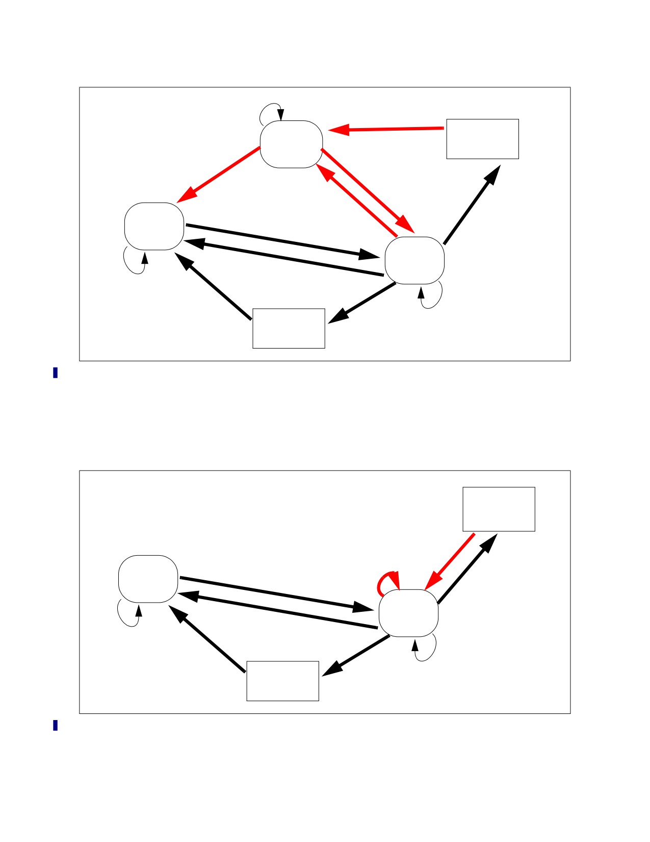
OPTIMIZATIONS FOR INTEL® AVX, INTEL® AVX2, AND INTEL® FMA
Execute SSE
Preserved
XSAVE’d Dirty
Execute Vzeroupper/
XRSTOR
Non-INIT
Image in Mem
Vzeroall/Xrstor w/ INIT
Penalty C
Upper State
Penalty D
Execute 256 or
128 Bit Intel AVX
Execute Intel SSE
Penalty B
Penalty A
Clean
Execute 256-bit Intel AVX
XSAVE w/o
UpperState
Vzero*
Dirty
Upper State
Execute Vzeroupper/
Execute Intel SSE
VzeroallXrstor w/ INIT
or 128-bit Intel AVX
Execute 256-bit
or 128-bit Intel AVX
XRSTOR
XSAVE’d Clean
XSAVE w/
Image in Mem
Vzero*
Figure 15-1. Intel® AVX—Intel® SSE Transitions in the Broadwell, and Prior Generation Microarchitectures
Table 15-2 lists the effect of mixing Intel AVX and Intel SSE code, with the bottom row indicating the
types of penalty that might arise depending on the initial YMM state (the row marked ‘Begin’) and the
ending state. Table 15-2 also includes the effect of transition penalty (Type C and D) associated with
restoring a dirty YMM state image stored in memory.
XSAVE’d Dirty
NON-INIT
Image in Mem
XRSTOR
Penalty C
Execute SSE
Penalty A
Clean
Execute 256-bit AVX
UpperState
XSAVE w/o
Vzero*
Dirty
Upper State
Execute Vzeroupper/
Execute SSE
VzeroallXrstor w/ INIT
or 128-bit AVX
Execute 256-bit
or 128-bit AVX
XRSTOR
XSAVE’d Clean
XSAVE w/
Image in Mem
Vzero*
Figure 15-2. Intel® AVX- Intel® SSE Transitions in the Skylake Microarchitecture
15-8

OPTIMIZATIONS FOR INTEL® AVX, INTEL® AVX2, AND INTEL® FMA
Table 15-2. State Transitions of Mixing AVX and SSE Code
Execute SSE
Execute AVX-128
Execute AVX-256
VZeroupper
XRSTOR
Begin
Clean
M/U
P/N
Clean
M/U
P/S
Clean
M/U
P/N
P/N
Dirty
Clean
Image
Image
End
Clean
P/N
P/N
Clean
M/U
M/U
M/U
M/U
M/U
Clean
P/N
Clean
Penalty
No
A
No
No
No
B
No
No
B
D
C
No
The magnitude of each type of transition penalty can vary across different microarchitectures. In Skylake
microarchitecture, some of the transition penalty is reduced. The transition diagram and associated
penalty is depicted in Figure 15-2. Table 15-3 gives approximate order of magnitude of the different
transition penalty types across recent microarchitectures.
Table 15-3. Approximate Magnitude of Intel® AVX—Intel® SSE Transition Penalties in Different
Microarchitectures
Type
Haswell
Broadwell
Skylake
Ice Lake Client
Microarchitecture
Microarchitecture
Microarchitecture
Microarchitecture
A
~XSAVE
~XSAVE
Partial Register
~XSAVE
Dependency + Blend
B
~XSAVE
~XSAVE
NA
~XSAVE
C
~Fraction of XSAVE
~Fraction of XSAVE
~XSAVE
~Fraction of XSAVE
D
~XSAVE
~XSAVE
NA
~XSAVE
To enable fast transitions between 256-bit Intel AVX and Intel SSE code blocks, use the VZEROUPPER
instruction before and after an AVX code block that would need to switch to execute SSE code. The VZER-
OUPPER instruction resets the upper 128 bits of all Intel AVX registers. This instruction has zero latency.
In addition, the processor changes back to a Clean state, after which execution of SSE instructions or
Intel AVX instructions has no transition penalty with prior microarchitectures. In Skylake microarchitec-
ture, the SSE block can executed from a Clean state without the penalty of upper-bits dependency and
blend operation.
128-bit Intel AVX instructions zero the upper 128-bits of the destination registers. Therefore, 128-bit and
256-bit Intel AVX instructions can be mixed with no penalty.
Assembly/Compiler Coding Rule 56. (H impact, H generality) Whenever a 256-bit AVX code
block and 128-bit SSE code block might execute in sequence, use the VZEROUPPER instruction to
facilitate a transition to a “Clean” state for the next block to execute from.
15.3.1 Mixing Intel® AVX and Intel SSE in Function Calls
Intel AVX to Intel SSE transitions can occur unexpectedly when calling functions or returning from func-
tions. For example, if a function that uses 256-bit Intel AVX, calls another function, the callee might be
using SSE code. Similarly, after a 256-bit Intel AVX function returns, the caller might be executing Intel
SSE code.
15-9

OPTIMIZATIONS FOR INTEL® AVX, INTEL® AVX2, AND INTEL® FMA
Assembly/Compiler Coding Rule 57. (H impact, H generality) Add VZEROUPPER instruction after
256-bit AVX instructions are executed and before any function call that might execute SSE code. Add
VZEROUPPER at the end of any function that uses 256-bit AVX instructions.
Example 15-4. Function Calls and Intel® AVX/Intel® SSE transitions
__attribute__((noinline)) void SSE_function()
{
__asm addps xmm1, xmm2
__asm xorps xmm3, xmm4
}
__attribute__((noinline)) void AVX_function_no_zeroupper()
{
__asm vaddps ymm1, ymm2, ymm3
__asm vxorps ymm4, ymm5, ymm6
}
__attribute__((noinline)) void AVX_function_with_zeroupper()
{
__asm vaddps ymm1, ymm2, ymm3
__asm vxorps ymm4, ymm5, ymm6
//add vzeroupper when returning from an AVX function
__asm vzeroupper
}
// Code encounter transition penalty
// Code mitigated transition penalty
__asm vaddps ymm1, ymm2, ymm3
__asm vaddps ymm1, ymm2, ymm3
//add vzeroupper before
//calling SSE function from AVX code
//penalty
__asm vzeroupper
//no penalty
SSE_function();
SSE_function();
AVX_function_no_zeroupper();
AVX_function_with_zeroupper();
//penalty
//no penalty
__asm addps xmm1, xmm2
__asm addps xmm1, xmm2
Table 15-2 summarizes a heuristic of the performance impact of using or not using VZEROUPPER to
bridge transitions of inter-function calls that changes between AVX code implementation and SSE code.
Table 15-4. Effect of VZEROUPPER with Inter-Function Calls Between AVX and SSE Code
Inter-Function Call
Prior Microarchitectures
Skylake Microarchitecture
With VZEROUPPER
1X (baseline)
~1
No VZEROUPPER
< 0.1X
Fraction of baseline
15.4
128-BIT LANE OPERATION AND AVX
256-bit operations in Intel AVX are generally performed in two halves of 128-bit lanes. Most of the 256-
bit Intel AVX instructions are defined as in-lane: the destination elements in each lane are calculated
using source elements only from the same lane. There are only a few cross-lane instructions, which are
described below.
15-10
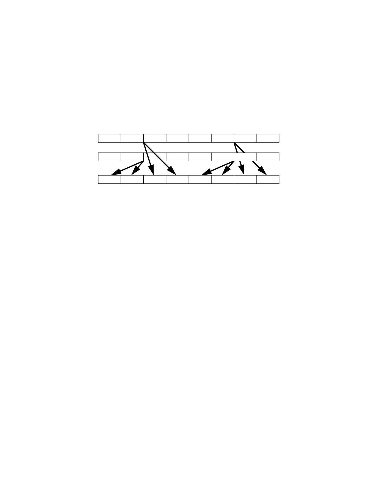
OPTIMIZATIONS FOR INTEL® AVX, INTEL® AVX2, AND INTEL® FMA
The majority of SSE computational instructions perform computation along vertical slots with each data
elements. The 128-bit lanes does not affect porting 128-bit code into 256-bit AVX code. VADDPS is one
example of this.
Many 128-bit SSE instruction moves data elements horizontally, e.g. SHUFPS uses an imm8 byte to
control the horizontal movement of data elements.
Intel AVX promotes these horizontal 128-bit SIMD instruction in-lane into 256-bit operation by using the
same control field within the low 128-bit land and the high 128-bit lane. For example, the 256-bit
VSHUFPS instruction uses a control byte containing 4 control values to select the source location of each
destination element in a 128-bit lane. This is shown below.
SRC1
X7
X6
X5
X4
X3
X2
X1
X0
SRC2
Y7
Y6
Y5
Y4
Y3
Y2
Y1
Y0
DEST
Y7 .. Y4
Y7 .. Y4
X7 .. X4
X7 .. X4
Y3 ..Y0
Y3 ..Y0
X3 .. X0
X3 .. X0
Imm8:
Imm[7:6] Imm[5:4] Imm[3:2] Imm[1:0] Imm[7:6] Imm[5:4] Imm[3:2] Imm[1:0]
Control Values 00b: X0/Y0 (Low lane), X4/Y4 (high lane)
Control Values 01b: X1/Y1 (Low lane), X5/Y5 (high lane)
Control Values 10b: X2/Y2 (Low lane), X6/Y6 (high lane)
Control Values 11b: X3/Y3 (Low lane), X7/Y7 (high lane)
15.4.1 Programming With the Lane Concept
Using the lane concept, algorithms implemented with SSE instruction set can be easily converted to use
256-bit Intel AVX. An SSE algorithm that executes iterations 0 to n can be converted such that the calcu-
lation of iteration i is done in the low lane and the calculation of iteration i+k is done in the high lane. For
consecutive iterations k equals one.
Some vectorized algorithms implemented with SSE instructions cannot use a simple conversion
described above. For example, shuffles that move elements within 16 bytes cannot be naturally
converted to shuffles with 32 byte since 32 byte shuffles can't cross lanes.
You can use the following instructions as building blocks for working with lanes:
• VINSERTF128 - insert packed floating-point values.
• VEXTRACTF128 - extract packed floating-point values.
• VPERM2F128 - permute floating-point values.
• VBROADCAST - load with broadcast.
The sections below describe two techniques: the strided loads and the cross register overlap. These
methods implement the in lane data arrangement described above and are useful in many algorithms
that initially seem to require cross lane calculations.
15-11
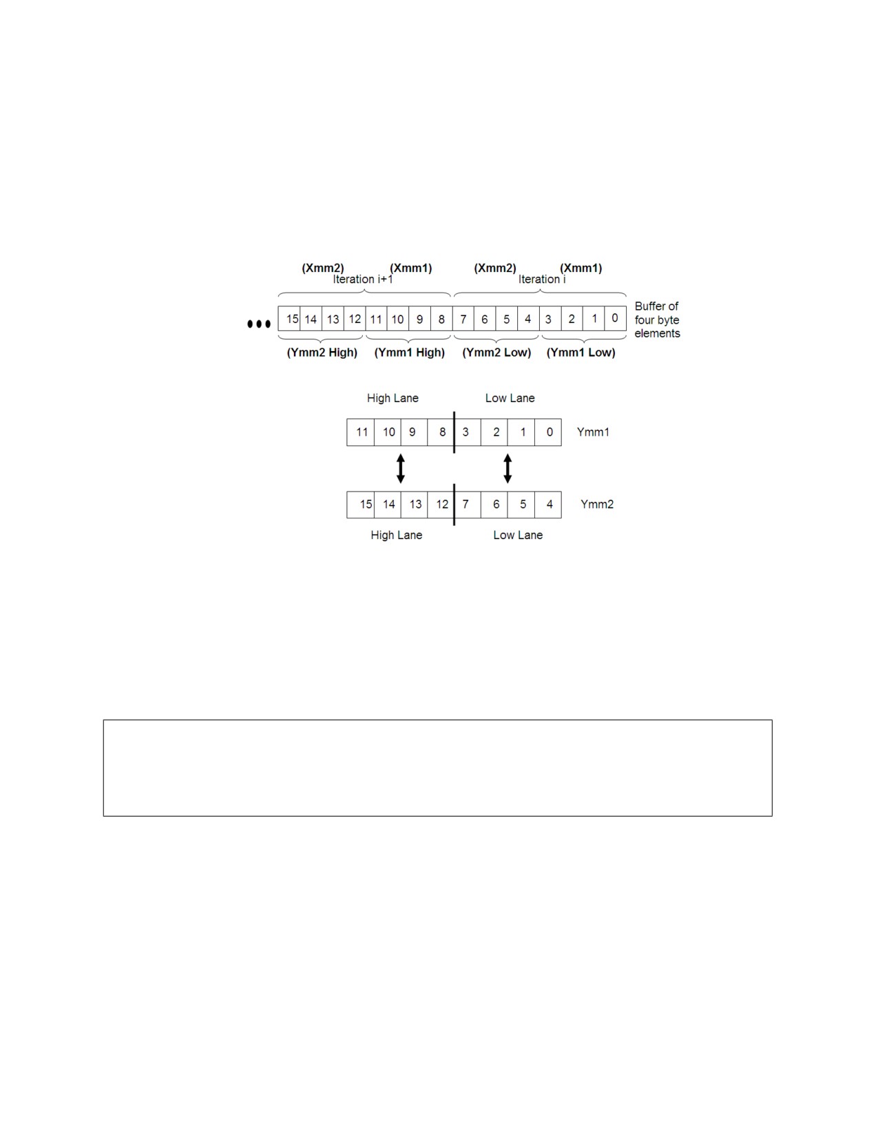
OPTIMIZATIONS FOR INTEL® AVX, INTEL® AVX2, AND INTEL® FMA
15.4.2 Strided Load Technique
The strided load technique is a programming method that uses Intel AVX instructions and is useful for
algorithms that involve unsupported cross-lane shuffles.
The method describes how to arrange data to avoid cross-lane shuffles. The main idea is to use 128-bit
loads in a way that mimics the corresponding Intel SSE algorithm, and enables the 256 Intel AVX instruc-
tions to execute iterations i of the loop in the low lanes and the iteration and i+k in the high lanes. In the
following example, k equals one.
The values in the low lanes of Ymm1 and Ymm2 in the figure above correspond to iteration i in the SSE
implementation. Similarly, the values in the high lanes of Ymm1 and Ymm2 correspond to iteration i+1.
The following example demonstrates the strided load method in a conversion of an Array of Structures
(AoS) to a Structure of Arrays (SoA). In this example, the input buffer contains complex numbers in an
AoS format. Each complex number is made of a real and an imaginary float values. The output buffer is
arranged as SoA. All the real components of the complex numbers are located at the first half of the
output buffer and all the imaginary components are located at the second half of the buffer. The following
pseudo code and figure illustrate the conversion:
Example 15-5. AoS to SoA Conversion of Complex Numbers in C Code
for (i = 0; i < N; i++)
{
Real[i] = Complex[i].Real;
Imaginary[i] = Complex[i].Imaginary;
}
15-12
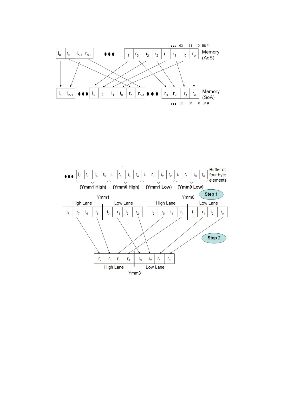
OPTIMIZATIONS FOR INTEL® AVX, INTEL® AVX2, AND INTEL® FMA
A simple extension of the Intel SSE algorithm from 16-byte to 32-byte operations would require cross-
lane data transition, as shown in the following figure. However, this is not possible with Intel AVX archi-
tecture and a different technique is required.
The challenge of cross-lane shuffle can be overcome with Intel AVX for AoS to SoA conversion. Using
VINSERTF128 to load 16 bytes to the appropriate lane in the YMM registers obviates the need for
cross-lane shuffle. Once the data is organized properly in the YMM registers for step 1, 32-byte VSHUFPS
can be used to move the data in lanes, as shown in step 2.
15-13

OPTIMIZATIONS FOR INTEL® AVX, INTEL® AVX2, AND INTEL® FMA
The following code compares the Intel SSE implementation of AoS to SoA with the 256-bit Intel AVX
implementation and demonstrates the performance gained.
Example 15-6. Aos to SoA Conversion of Complex Numbers Using Intel® AVX
Intel® SSE Code
Intel® AVX Code
xor rbx, rbx
xor rbx, rbx
xor rdx, rdx
xor rdx, rdx
mov rcx, len
mov rcx, len
mov rdi, inPtr
mov rdi, inPtr
mov rsi, outPtr1
mov rsi, outPtr1
mov rax, outPtr2
mov rax, outPtr2
loop1:
loop1:
movups xmm0, [rdi+rbx]
vmovups xmm0, [rdi+rbx]
//i1 r1 i0 r0
//i1 r1 i0 r0
movups xmm1, [rdi+rbx+16]
vmovups xmm1, [rdi+rbx+16]
// i3 r3 i2 r2
// i3 r3 i2 r2
movups xmm2, xmm0
vinsertf128 ymm0, ymm0, [rdi+rbx+32] , 1
//i5 r5 i4 r4; i1 r1 i0 r0
shufps xmm0, xmm1, 0xdd
vinsertf128 ymm1, ymm1, [rdi+rbx+48] , 1
//i3 i2 i1 i0
//i7 r7 i6 r6; i3 r3 i2 r2
shufps xmm2, xmm1, 0x88
vshufps ymm2, ymm0, ymm1, 0xdd
//r3 r2 r1 r0
//i7 i6 i5 i4; i3 i2 i1 i0
vshufps ymm3, ymm0, ymm1, 0x88
//r7 r6 r5 r4; r3 r2 r1 r0
movups [rax+rdx], xmm0
vmovups [rax+rdx], ymm2
movups [rsi+rdx], xmm2
vmovups [rsi+rdx], ymm3
add rdx, 16
add rdx, 32
add rbx, 32
add rbx, 64
cmp rcx, rbx
cmp rcx, rbx
jnz loop1
jnz loop1
15.4.3 The Register Overlap Technique
The register overlap technique is useful for algorithms that use shuffling. Similar to the strided load tech-
nique, the register overlap technique arranges data to avoid cross-lane shuffles.
This technique is useful for algorithm that process continues data, which is partially shared by sequential
iterations. The following figure illustrates the desired data layout. This is enabled by using overlapping
256-bit loads, or by using the VPERM2F128 instruction.
15-14
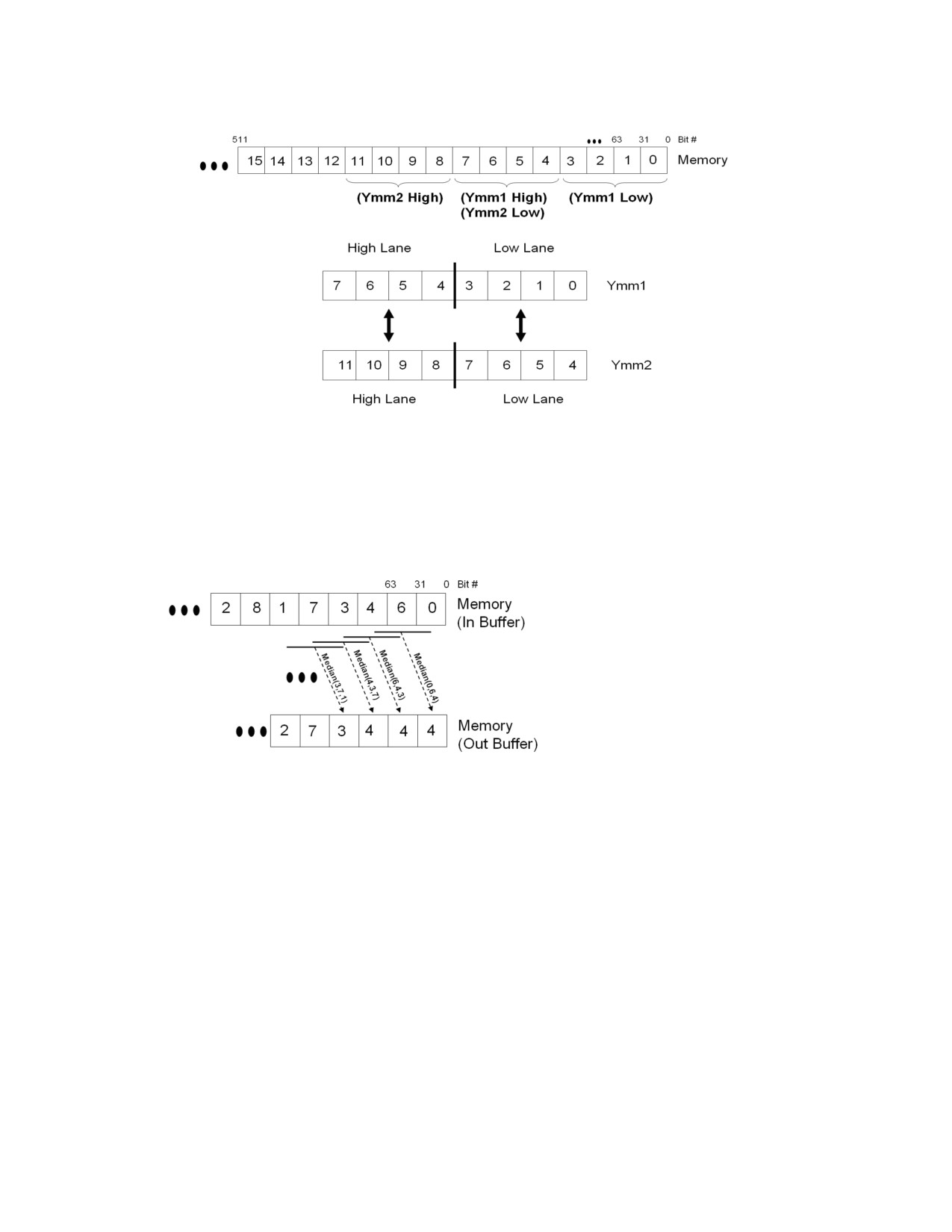
OPTIMIZATIONS FOR INTEL® AVX, INTEL® AVX2, AND INTEL® FMA
The Median3 code sample below demonstrates the register overlap technique. The median3 technique
calculates the median of every three consecutive elements in a vector.
Y[i] = Median( X[i], X[i+1], X[i+2] )
Where Y is the output vector and X is the input vector. The following figure illustrates the calculation done
by the median algorithm.
15-15

OPTIMIZATIONS FOR INTEL® AVX, INTEL® AVX2, AND INTEL® FMA
Following are three implementations of the Median3 algorithm:
• Alternative 1 is the Intel SSE implementation.
• Alternatives 2 and 3 implement the register overlap technique in two ways.
— Alternative 2 loads the data from the input buffer into the YMM registers using overlapping 256-
bit load operations.
— Alternative 3 loads the data from the input buffer into the YMM registers using a 256-bit load
operation and VPERM2F128.
— Alternatives 2 and 3 gain performance by using wider vectors.
Example 15-7. Register Overlap Method for Median of 3 Numbers
1: SSE Code
2: 256-bit AVX w/ Overlapping Loads
3: 256-bit AVX with VPERM2F128
xor ebx, ebx
xor ebx, ebx
xor ebx, ebx
mov rcx, len
mov rcx, len
mov rcx, len
mov rdi, inPtr
mov rdi, inPtr
mov rdi, inPtr
mov rsi, outPtr
mov rsi, outPtr
mov rsi, outPtr
movaps xmm0, [rdi]
vmovaps ymm0, [rdi]
vmovaps ymm0, [rdi]
loop_start:
loop_start:
loop_start:
movaps xmm4, [rdi+16]
vshufps ymm2, ymm0,
add rdi, 32
movaps xmm2, [rdi]
[rdi+16], 0x4E
vmovaps ymm6, [rdi]
movaps xmm1, [rdi]
vshufps ymm1, ymm0,
vperm2f128 ymm1, ymm0, ymm6, 0x21
movaps xmm3, [rdi]
ymm2, 0x99
vshufps ymm3, ymm0, ymm1, 0x4E
add rdi, 16
add rbx, 8
vshufps ymm2, ymm0, ymm3, 0x99
add rbx, 4
add rdi, 32
add rbx, 8
shufps xmm2, xmm4, 0x4e
vminps ymm5, ymm0, ymm2
shufps xmm1, xmm2, 0x99
vminps ymm4, ymm0, ymm1
vmaxps ymm0, ymm0, ymm2
minps xmm3, xmm1
vmaxps ymm0, ymm0, ymm1
vminps ymm4, ymm0, ymm3
maxps xmm0, xmm1
vminps ymm3, ymm0, ymm2
vmaxps ymm7, ymm4, ymm5
minps xmm0, xmm2
vmaxps ymm5, ymm3, ymm4
vmovaps ymm0, ymm6
maxps xmm0, xmm3
vmovaps [rsi], ymm5
vmovaps [rsi], ymm7
movaps [rsi], xmm0
add rsi, 32
add rsi, 32
movaps xmm0, xmm4
vmovaps ymm0, [rdi]
cmp rbx, rcx
add rsi, 16
cmp rbx, rcx
jl
loop_start
cmp rbx, rcx
jl
loop_start
jl
loop_start
15.5
DATA GATHER AND SCATTER
This section describes techniques for implementing data gather and scatter operations using Intel AVX
instructions.
15.5.1 Data Gather
The gather operation reads elements from an input buffer based on indexes specified in an index buffer.
The gathered elements are written in an output buffer. The following figure illustrates an example for a
gather operation.
15-16
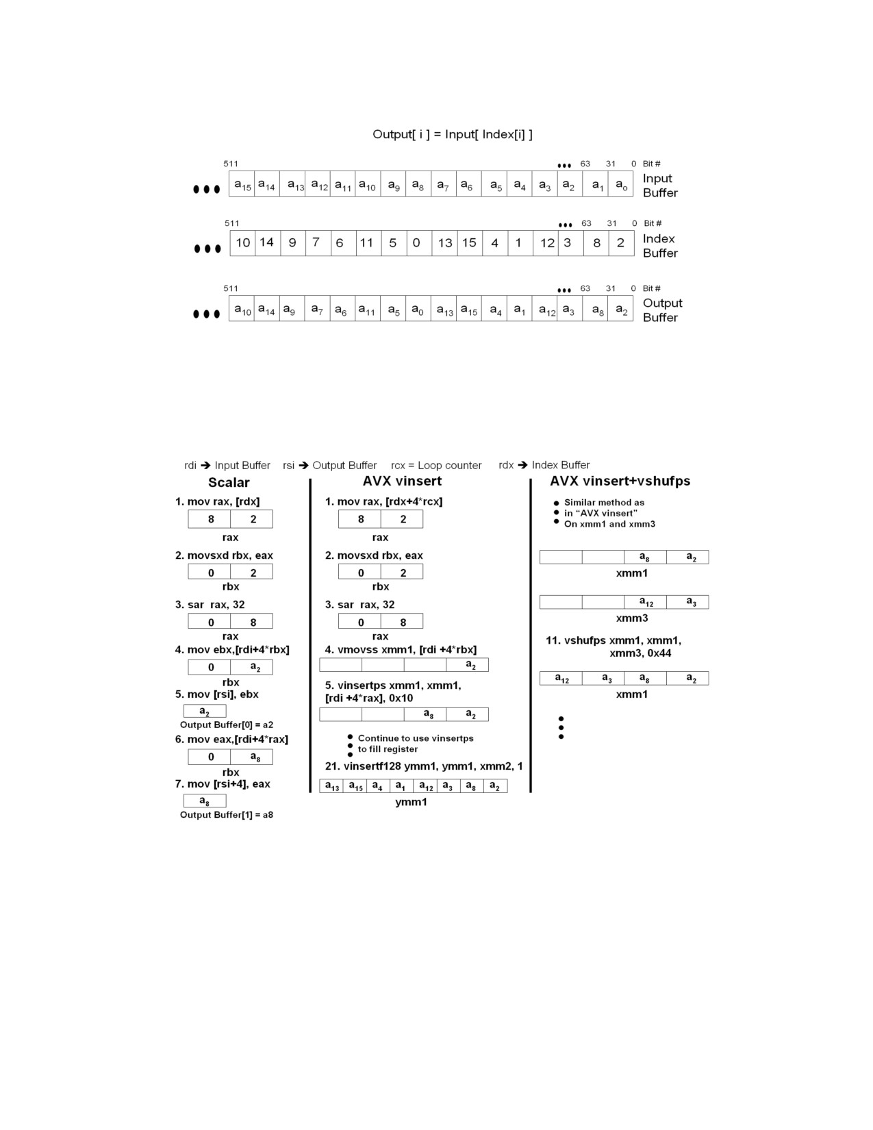
OPTIMIZATIONS FOR INTEL® AVX, INTEL® AVX2, AND INTEL® FMA
Following are 3 implementations for the gather operation from an array of 4 byte elements. Alternative 1
is a scalar implementation using general purpose registers. Alternative 2 and 3 use Intel AVX instruc-
tions. The figure below shows code snippets from Example 15-8 assuming that it runs the first iteration
on data from the previous figure.
Performance of the Intel AVX examples is similar to the performance of a corresponding Intel SSE imple-
mentation. The table below shows the three gather implementations.
15-17

OPTIMIZATIONS FOR INTEL® AVX, INTEL® AVX2, AND INTEL® FMA
Example 15-8. Data Gather - Intel® AVX versus Scalar Code
1: Scalar Code
2: Intel® AVX w/ VINSERTPS
3: VINSERTPS+VSHUFPS
mov rdi, InBuf
mov rdi, InBuf
mov rdi, InBuf
mov rsi, OutBuf
mov rsi, OutBuf
mov rsi, OutBuf
mov rdx, Index
mov rdx, Index
mov rdx, Index
xor
rcx, rcx
xor
rcx, rcx
xor
rcx, rcx
loop1:
loop1:
loop1:
mov rax, [rdx]
mov rax, [rdx + 4*rcx]
mov rax, [rdx + 4*rcx]
movsxd rbx, eax
movsxd rbx, eax
movsxd rbx, eax
sar rax, 32
sar rax, 32
sar rax, 32
mov ebx, [rdi + 4*rbx]
vmovss xmm1, [rdi + 4*rbx]
vmovss xmm1, [rdi + 4*rbx]
mov [rsi], ebx
vinsertps xmm1, xmm1,
vinsertps xmm1, xmm1,
mov eax, [rdi + 4*rax]
[rdi + 4*rax], 0x10
[rdi + 4*rax], 0x10
mov [rsi + 4], eax
mov rax, [rdx + 8 + 4*rcx]
mov rax, [rdx + 8 + 4*rcx]
movsxd rbx, eax
movsxd rbx, eax
mov rax, [rdx + 8]
sar rax, 32
sar rax, 32
movsxd rbx, eax
vinsertps xmm1, xmm1,
vmovss xmm3, [rdi + 4*rbx]
sar rax, 32
[rdi + 4*rbx], 0x20
vinsertps xmm3, xmm3,
mov ebx, [rdi + 4*rbx]
[rdi + 4*rax], 0x10
mov [rsi + 8], ebx
vinsertps xmm1, xmm1,
mov eax, [rdi + 4*rax]
[rdi + 4*rax], 0x30
vshufps xmm1, xmm1,
mov [rsi + 12], eax
xmm3, 0x44
mov rax, [rdx + 16]
mov rax, [rdx + 16 + 4*rcx]
mov rax, [rdx + 16 + 4*rcx]
movsxd rbx, eax
movsxd rbx, eax
movsxd rbx, eax
sar rax, 32
sar rax, 32
sar rax, 32
mov ebx, [rdi + 4*rbx]
vmovss xmm2, [rdi + 4*rbx]
vmovss xmm2, [rdi + 4*rbx]
mov [rsi + 16], ebx
vinsertps xmm2, xmm2,
vinsertps xmm2, xmm2,
mov eax, [rdi + 4*rax]
[rdi + 4*rax ], 0x10
[rdi + 4*rax ], 0x10
mov [rsi + 20], eax
mov rax, [rdx + 24 + 4*rcx]
mov rax, [rdx + 24 + 4*rcx]
mov rax, [rdx + 24]
movsxd rbx, eax
movsxd rbx, eax
movsxd rbx, eax
sar rax, 32
sar rax, 32
sar rax, 32
vinsertps xmm2, xmm2,
vmovss xmm4, [rdi + 4*rbx]
mov ebx, [rdi + 4*rbx]
[rdi + 4*rbx], 0x20
vinsertps xmm4, xmm4,
mov [rsi + 24], ebx
[rdi + 4*rax], 0x10
mov eax, [rdi + 4*rax]
vinsertps xmm2, xmm2,
mov [rsi + 28], eax
[rdi + 4*rax], 0x30
vshufps xmm2, xmm2,
xmm4, 0x44
add rsi, 32
vinsertf128 ymm1, ymm1,
add rdx, 32
xmm2, 1
vinsertf128 ymm1, ymm1,
add rcx, 8
xmm2, 1
cmp rcx, len
vmovaps [rsi + 4*rcx], ymm1
jl
loop1
add
rcx, 8
vmovaps [rsi + 4*rcx], ymm1
cmp
rcx, len
add rcx, 8
jl
loop1
cmp rcx, len
jl
loop1
15-18
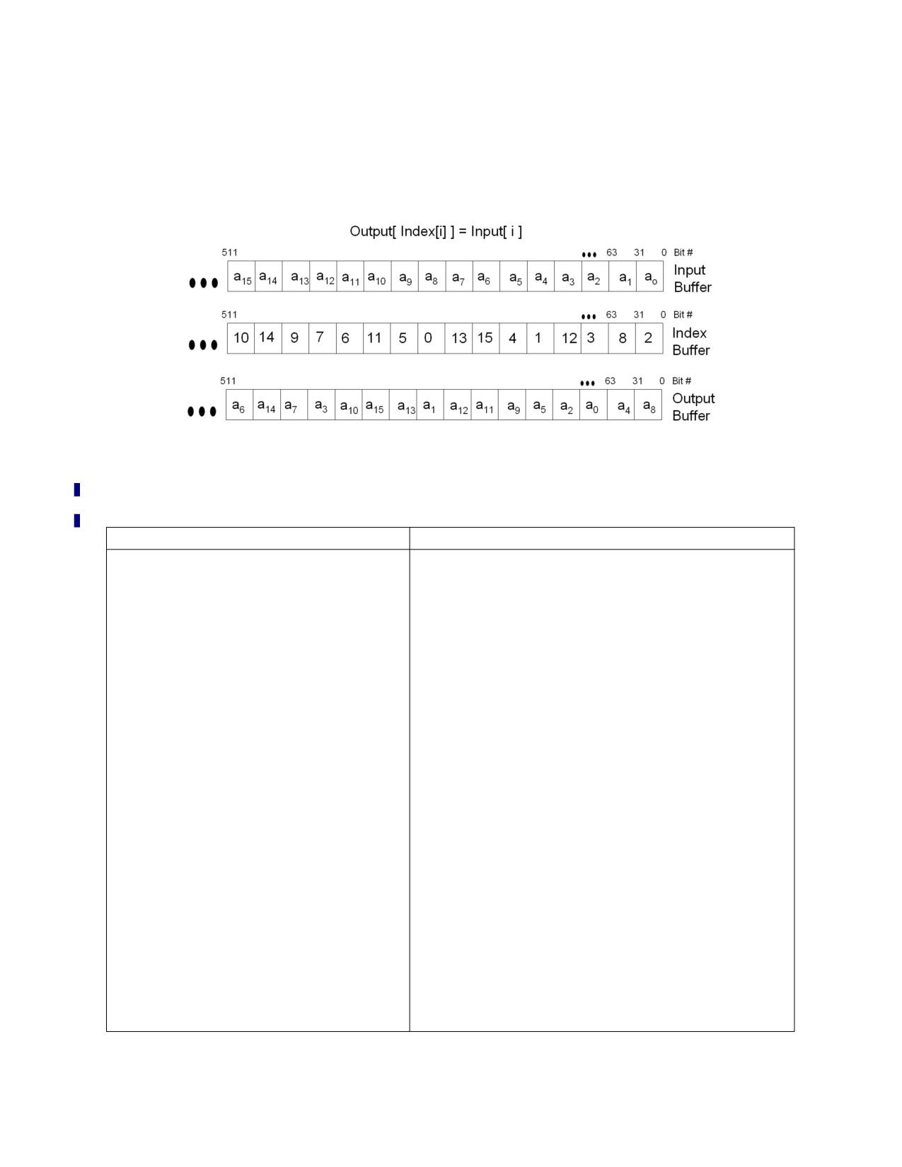
OPTIMIZATIONS FOR INTEL® AVX, INTEL® AVX2, AND INTEL® FMA
15.5.2 Data Scatter
The scatter operation reads elements from an input buffer sequentially. It then writes them to an output
buffer based on indexes specified in an index buffer. The following figure illustrates an example for a
scatter operation.
The following table includes a scalar implementation and an Intel AVX implementation of a scatter
sequence. The Intel AVX examples consist mainly of 128-bit Intel AVX instructions. Performance of the
Intel AVX examples is similar to the performance of corresponding Intel SSE implementation.
Example 15-9. Scatter Operation Using Intel® AVX
Scalar Code
AVX Code
mov rdi, InBuf
mov rdi, InBuf
mov rsi, OutBuf
mov rsi, OutBuf
mov rdx, Index
mov rdx, Index
xor
rcx, rcx
xor
rcx, rcx
loop1:
loop1:
movsxd rax, [rdx]
vmovaps ymm0, [rdi + 4*rcx]
mov ebx, [rdi]
movsxd rax, [rdx + 4*rcx]
mov [rsi + 4*rax], ebx
movsxd rbx, [rdx + 4*rcx + 4]
movsxd rax, [rdx + 4]
vmovss
[rsi + 4*rax], xmm0
mov ebx, [rdi + 4]
movsxd rax, [rdx + 4*rcx + 8]
mov [rsi + 4*rax], ebx
vpalignr xmm1, xmm0, xmm0, 4
movsxd rax, [rdx + 8]
vmovss
[rsi + 4*rbx], xmm1
mov ebx, [rdi + 8]
movsxd rbx, [rdx + 4*rcx + 12]
mov [rsi + 4*rax], ebx
vpalignr xmm2, xmm0, xmm0, 8
movsxd rax, [rdx + 12]
vmovss
[rsi + 4*rax], xmm2
mov ebx, [rdi + 12]
movsxd rax, [rdx + 4*rcx + 16]
mov [rsi + 4*rax], ebx
vpalignr xmm3, xmm0, xmm0, 12
movsxd rax, [rdx + 16]
vmovss
[rsi + 4*rbx], xmm3
mov ebx, [rdi + 16]
movsxd rbx, [rdx + 4*rcx + 20]
mov [rsi + 4*rax], ebx
vextractf128 xmm0, ymm0, 1
movsxd rax, [rdx + 20]
vmovss
[rsi + 4*rax], xmm0
mov ebx, [rdi + 20]
movsxd rax, [rdx + 4*rcx + 24]
mov [rsi + 4*rax], ebx
vpalignr xmm1, xmm0, xmm0, 4
movsxd rax, [rdx + 24]
vmovss
[rsi + 4*rbx], xmm1
mov ebx, [rdi + 24]
movsxd rbx, [rdx + 4*rcx + 28]
15-19
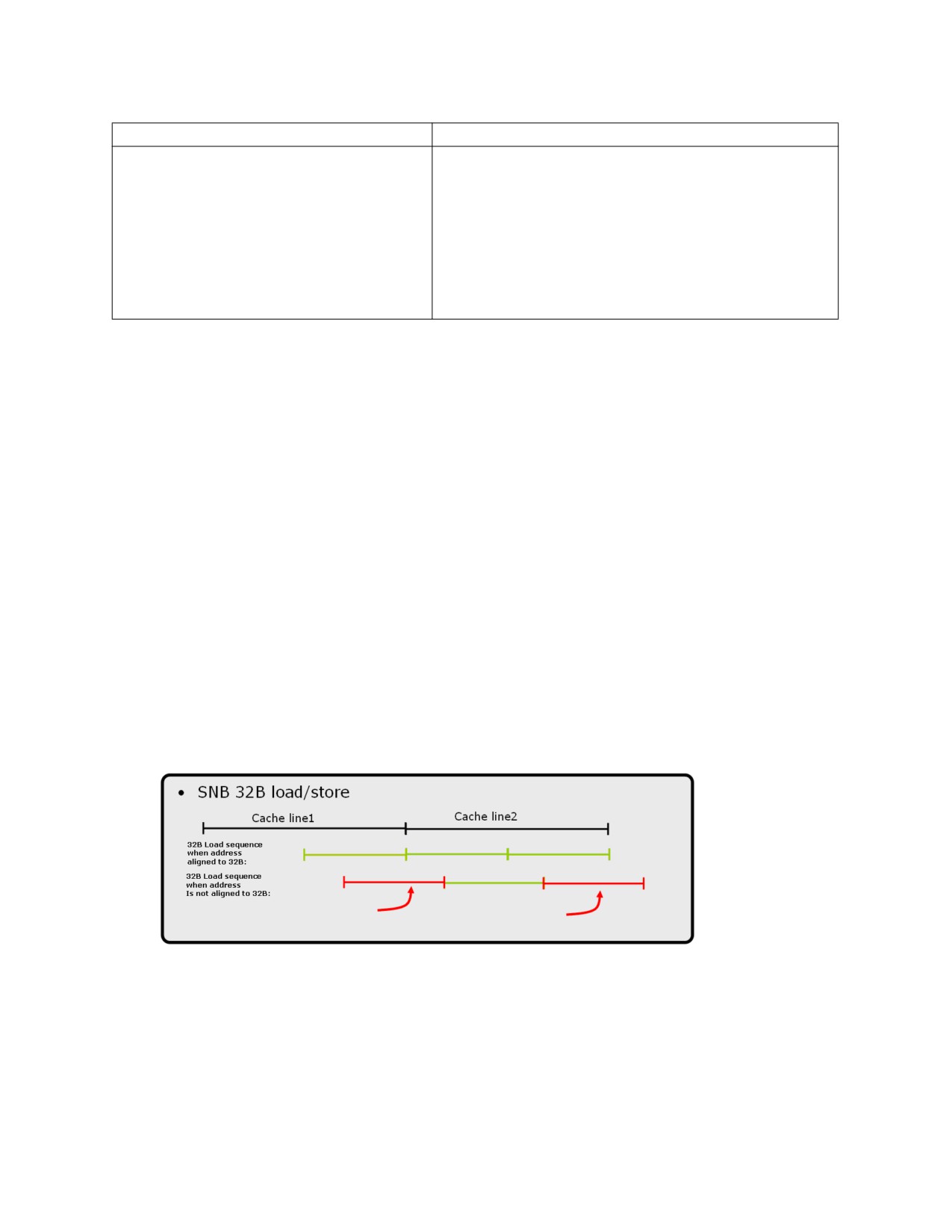
OPTIMIZATIONS FOR INTEL® AVX, INTEL® AVX2, AND INTEL® FMA
Example 15-9. Scatter Operation Using Intel® AVX (Contd.)
Scalar Code
AVX Code
mov [rsi + 4*rax], ebx
vpalignr xmm2, xmm0, xmm0, 8
movsxd rax, [rdx + 28]
vmovss
[rsi + 4*rax], xmm2
mov ebx, [rdi + 28]
vpalignr xmm3, xmm0, xmm0, 12
mov [rsi + 4*rax], ebx
vmovss
[rsi + 4*rbx], xmm3
add
rdi, 32
add
rcx, 8
add
rdx, 32
cmp
rcx, len
add
rcx, 8
jl
loop1
cmp
rcx, len
jl
loop1
15.6
DATA ALIGNMENT FOR INTEL® AVX
This section explains the benefit of aligning data that is used by Intel AVX instructions and proposes some
methods to improve performance when such alignment is not possible. Most examples in this section are
variations of the SAXPY kernel. SAXPY is the Scalar Alpha * X + Y algorithm.
The C code below is a C implementation of SAXPY.
for (int i = 0; i < n; i++)
{ c[i] = alpha * a[i] + b[i]; }
15.6.1 Align Data to 32 Bytes
Aligning data to vector length is recommended. When using 16-byte SIMD instructions, loaded data
should be aligned to 16 bytes. Similarly, for best results when using Intel AVX instructions with 32-byte
registers align the data to 32-bytes.
When using Intel AVX with unaligned 32-byte vectors, every second load is a cache-line split, since the
cache-line is 64 bytes. This doubles the cache line split rate compared to Intel SSE code that uses 16-
byte vectors. Even though split line access penalties have been reduced significantly since Nehalem
microarchitecture, a high cache-line split rate in memory-intensive code may cause performance degra-
dation.
15-20

OPTIMIZATIONS FOR INTEL® AVX, INTEL® AVX2, AND INTEL® FMA
Example 15-10. SAXPY using Intel® AVX
mov
rax, src1
mov
rbx, src2
mov
rcx, dst
mov
rdx, len
xor
rdi, rdi
vbroadcastss
ymm0, alpha
start_loop:
vmovups
ymm1, [rax + rdi]
vmulps
ymm1, ymm1, ymm0
vmovups
ymm2, [rbx + rdi]
vaddps
ymm1, ymm1, ymm2
vmovups
[rcx + rdi], ymm1
vmovups
ymm1, [ rax + rdi + 32]
vmulps
ymm1, ymm1, ymm0
vmovups
ymm2, [rbx + rdi + 32]
vaddps
ymm1, ymm1, ymm2
vmovups
[rcx + rdi + 32], ymm1
add
rdi, 64
cmp
rdi, rdx
jl
start_loop
SAXPY is a memory intensive kernel that emphasizes the importance of data alignment. Optimal perfor-
mance requires both data source address to be 32-byte aligned and destination address also 32-byte
aligned. If only one of the three address is not aligned to 32-byte boundary, the performance may be
halved. If all three addresses are mis-aligned relative to 32 byte, the performance degrades further. In
some cases, unaligned accesses may result in lower performance for Intel AVX code compared to Intel
SSE code. Other Intel AVX kernels typically have more computation which can reduce the effect of the
data alignment penalty.
Assembly/Compiler Coding Rule 58. (H impact, M generality) Align data to 32-byte boundary
when possible. Prefer store alignment over load alignment.
You can use dynamic data alignment using the _mm_malloc intrinsic instruction with the Intel®
Compiler, or _aligned_malloc of the Microsoft* Compiler. For example:
//dynamically allocating 32byte aligned buffer with 2048 float elements.
InputBuffer = (float*) _mm_malloc (2048*sizeof(float), 32);
You can use static data alignment using __declspec(align(32)). For example:
//Statically allocating 32byte aligned buffer with 2048 float elements.
__declspec(align(32)) float InputBuffer[2048];
15.6.2 Consider 16-Byte Memory Access when Memory is Unaligned
For best results use Intel AVX 32-byte loads and align data to 32-bytes. However, there are cases where
you cannot align the data, or data alignment is unknown. This can happen when you are writing a library
function and the input data alignment is unknown. In these cases, using 16-byte memory accesses may
be the best alternative. The following method uses 16-byte loads while still benefiting from the 32-byte
YMM registers.
15-21

OPTIMIZATIONS FOR INTEL® AVX, INTEL® AVX2, AND INTEL® FMA
NOTE
Beginning with Skylake microarchitecture, this optimization is not necessary. The only
case where 16-byte loads may be more efficient is when the data is 16-byte aligned but
not 32-byte aligned. In this case 16-byte loads might be preferable as no cache line split
memory accesses are issued.
Consider replacing unaligned 32-byte memory accesses using a combination of VMOVUPS,
VINSERTF128, and VEXTRACTF128 instructions.
Example 15-11. Using 16-Byte Memory Operations for Unaligned 32-Byte Memory Operation
Convert 32-byte loads as follows:
vmovups
ymm0, mem
-> vmovups xmm0, mem
vinsertf128 ymm0, ymm0, mem+16, 1
Convert 32-byte stores as follows:
vmovups mem, ymm0
-> vmovups mem, xmm0
vextractf128 mem+16, ymm0, 1
The following intrinsics are available to handle unaligned 32-byte memory operating using 16-byte memory accesses:
_mm256_loadu2_m128 ( float const * addr_hi, float const * addr_lo);
_mm256_loadu2_m128d ( double const * addr_hi, double const * addr_lo);
_mm256_loadu2_m128 i( __m128i const * addr_hi, __m128i const * addr_lo);
_mm256_storeu2_m128 ( float * addr_hi, float * addr_lo, __m256 a);
_mm256_storeu2_m128d ( double * addr_hi, double * addr_lo, __m256d a);
_mm256_storeu2_m128 i( __m128i * addr_hi, __m128i * addr_lo, __m256i a);
Example 15-12 shows two implementations for SAXPY with unaligned addresses. Alternative 1 uses 32-
byte loads and alternative 2 uses 16-byte loads. These code samples are executed with two source
buffers, src1, src2, at 4 byte offset from 32-byte alignment, and a destination buffer, DST, that is 32-byte
aligned. Using two 16-byte memory operations in lieu of 32-byte memory access performs faster.1
Example 15-12. SAXPY Implementations for Unaligned Data Addresses
AVX with 32-byte memory operation
AVX using two 16-byte memory operations
mov
rax, src1
mov
rax, src1
mov
rbx, src2
mov
rbx, src2
mov
rcx, dst
mov
rcx, dst
mov
rdx, len
mov
rdx, len
xor
rdi, rdi
xor
rdi, rdi
vbroadcastss ymm0, alpha
vbroadcastss ymm0, alpha
start_loop:
start_loop:
vmovups ymm1, [rax + rdi]
vmovups xmm2, [rax+rdi]
vmulps ymm1, ymm1, ymm0
vinsertf128 ymm2, ymm2, [rax+rdi+16], 1
vmovups ymm2, [rbx + rdi]
vmulps ymm1, ymm0, ymm2
vaddps ymm1, ymm1, ymm2
vmovups xmm2, [ rbx + rdi]
vmovups [rcx + rdi], ymm1
vinsertf128 ymm2, ymm2, [rbx+rdi+16], 1
vaddps ymm1, ymm1, ymm2
1. Beginning with Haswell microarchitecture and onward, it is better to read the entire register: 32-byte register or 64-
byte register (with the availability of Intel® AVX-512).
15-22

OPTIMIZATIONS FOR INTEL® AVX, INTEL® AVX2, AND INTEL® FMA
Example 15-12. SAXPY Implementations for Unaligned Data Addresses (Contd.)
AVX with 32-byte memory operation
AVX using two 16-byte memory operations
vmovups [rcx+rdi], ymm1
vmovups ymm1, [rax+rdi+32]
vmovups xmm2, [rax+rdi+32]
vmulps ymm1, ymm1, ymm0
vinsertf128 ymm2, ymm2, [rax+rdi+48], 1
vmulps ymm1, ymm0, ymm2
vmovups ymm2, [rbx+rdi+32]
vmovups xmm2, [rbx+rdi+32]
vaddps ymm1, ymm1, ymm2
vinsertf128 ymm2, ymm2, [rbx+rdi+48], 1
vmovups [rcx+rdi+32], ymm1
vaddps ymm1, ymm1, ymm2
vmovups [rcx+rdi+32], ymm1
add
rdi, 64
add rdi, 64
cmp
rdi, rdx
cmp rdi, rdx
jl
start_loop
jl start_loop
Assembly/Compiler Coding Rule 59. (M impact, H generality) Align data to 32-byte boundary
when possible. If it is not possible to align both loads and stores, then prefer store alignment over load
alignment.
15.6.3 Prefer Aligned Stores Over Aligned Loads
There are cases where it is possible to align only a subset of the processed data buffers. In these cases,
aligning data buffers used for store operations usually yields better performance than aligning data
buffers used for load operations.
Unaligned stores are likely to cause greater performance degradation than unaligned loads, since there
is a very high penalty on stores to a split cache-line that crosses pages. This penalty is estimated at 150
cycles. Stores that cross a page boundary are executed at retirement. In Example 15-12, unaligned store
address can affect SAXPY performance for 3 unaligned addresses to about one quarter of the aligned
case.
15.7
L1D CACHE LINE REPLACEMENTS
NOTE
Beginning with Haswell microarchitecture, cache line replacement is no longer a concern .
When a load misses the L1D Cache, a cache line with the requested data is brought from a higher
memory hierarchy level. In memory intensive code where the L1D Cache is always active, replacing a
cache line in the L1D Cache may delay other loads. In Sandy Bridge and Ivy Bridge microarchitectures,
the penalty for 32-Byte loads may be higher than the penalty for 16-Byte loads. Therefore, memory
intensive Intel AVX code with 32-Byte loads and with data set larger than the L1D Cache may be slower
than similar code with 16-Byte loads.
When Example 15-12 is run with a data set that resides in the L2 Cache, the 16-byte memory access
implementation is slightly faster than the 32-byte memory operation.
Be aware that the relative merit of 16-byte memory accesses versus 32-byte memory access is imple-
mentation specific across generations of microarchitectures.
In Haswell microarchitecture, the L1D Cache can support two 32-byte fetch each cycle.
15-23
OPTIMIZATIONS FOR INTEL® AVX, INTEL® AVX2, AND INTEL® FMA
15.8
4K ALIASING
4-KByte memory aliasing occurs when the code stores to one memory location and shortly after that it
loads from a different memory location with a 4-KByte offset between them. For example, a load to linear
address 0x400020 follows a store to linear address 0x401020.
The load and store have the same value for bits 5 - 11 of their addresses and the accessed byte offsets
should have partial or complete overlap.
4K aliasing may have a five-cycle penalty on the load latency. This penalty may be significant when 4K
aliasing happens repeatedly and the loads are on the critical path. If the load spans two cache lines it
might be delayed until the conflicting store is committed to the cache. Therefore 4K aliasing that happens
on repeated unaligned Intel AVX loads incurs a higher performance penalty.
To detect 4K aliasing, use the LD_BLOCKS_PARTIAL.ADDRESS_ALIAS event that counts the number of
times Intel AVX loads were blocked due to 4K aliasing.
To resolve 4K aliasing, try the following methods in the following order:
• Align data to 32 Bytes.
• Change offsets between input and output buffers if possible.
• Sandy Bridge and Ivy Bridge microarchitectures may benefit from using 16-Byte memory accesses
on memory which is not 32-Byte aligned.
15.9
CONDITIONAL SIMD PACKED LOADS AND STORES
The VMASKMOV instruction conditionally moves packed data elements to/from memory, depending on
the mask bits associated with each data element. The mask bit for each data element is the most signif-
icant bit of the corresponding element in the mask register.
When performing a mask load, the returned value is 0 for elements which have a corresponding mask
value of 0. The mask store instruction writes to memory only the elements with a corresponding mask
value of 1, while preserving memory values for elements with a corresponding mask value of 0. Faults
can occur only for memory accesses that are required by the mask. Faults do not occur due to refer-
encing any memory location if the corresponding mask bit value for that memory location is zero. For
example, no faults are detected if the mask bits are all zero.
The following figure shows an example for a mask load and a mask store which does not cause a fault. In
this example, the mask register for the load operation is ymm1 and the mask register for the store oper-
ation is ymm2.
When using masked load or store consider the following:
• On processors based on microarchitectures prior to Skylake, the address of a VMASKMOV store is
considered as resolved only after the mask is known. Loads that follow a masked store may be
blocked, depending on the memory disambiguation prediction, until the mask value is known.
• If the mask is not all 1 or all 0, loads that depend on the masked store have to wait until the store
data is written to the cache. If the mask is all 1 the data can be forwarded from the masked store to
the dependent loads. If the mask is all 0 the loads do not depend on the masked store.
15-24
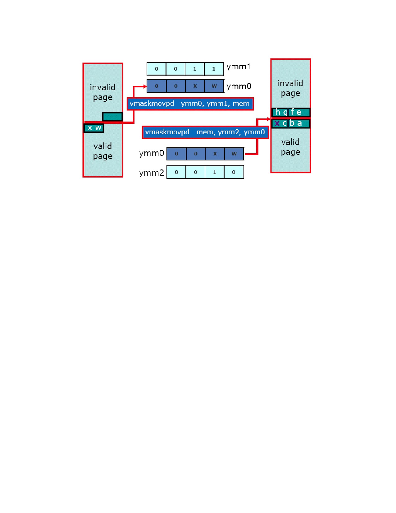
OPTIMIZATIONS FOR INTEL® AVX, INTEL® AVX2, AND INTEL® FMA
• Masked loads including an illegal address range do not result in an exception if the range is under a
zero mask value. However, the processor may take a multi-hundred-cycle “assist” to determine that
no part of the illegal range have a one mask value. This assist may occur even when the mask is
“zero” and it seems obvious to the programmer that the load should not be executed.
When using VMASKMOV, consider the following:
• Use VMASKMOV only in cases where VMOVUPS cannot be used.
• Use VMASKMOV on 32Byte aligned addresses if possible.
• If possible use valid address range for masked loads, even if the illegal part is masked with zeros.
• Determine the mask as early as possible.
• Avoid store-forwarding issues by performing loads prior to a VMASKMOV store if possible.
• Be aware of mask values that would cause the VMASKMOV instruction to require assist (if an assist is
required, the latency of VMASKMOV to load data will increase dramatically):
— Load data using VMASKMOV with a mask value selecting 0 elements from an illegal address will
require an assist.
— Load data using VMASKMOV with a mask value selecting 0 elements from a legal address
expressed in some addressing form (e.g. [base+index], disp[base+index] )will require an assist.
With processors based on the Skylake microarchitecture, the performance characteristics of VMASKMOV
instructions have the following notable items:
• Loads that follow a masked store is not longer blocked until the mask value is known.
• Store data using VMASKMOV with a mask value permitting 0 elements to be written to an illegal
address will require an assist.
15.9.1 Conditional Loops
VMASKMOV enables vectorization of loops that contain conditional code. There are two main benefits in
using VMASKMOV over the scalar implementation in these cases:
• VMASKMOV code is vectorized.
• Branch mispredictions are eliminated.
Below is a conditional loop C code:
15-25

OPTIMIZATIONS FOR INTEL® AVX, INTEL® AVX2, AND INTEL® FMA
Example 15-13. Loop with Conditional Expression
for(int i = 0; i < miBufferWidth; i++)
{
if(A[i]>0)
{
B[i] = (E[i]*C[i]);
}
else
{
B[i] = (E[i]*D[i]);
}
}
Example 15-14. Handling Loop Conditional with VMASKMOV
Scalar
AVX using VMASKMOV
float* pA = A;
float* pA = A;
float* pB = B;
float* pB = B;
float* pC = C;
float* pC = C;
float* pD = D;
float* pD = D;
float* pE = E;
float* pE = E;
uint64 len = (uint64) (miBuffer-
uint64 len = (uint64) (miBufferWidth)*sizeof(float);
Width)*sizeof(float);
__asm
__asm
{
{
mov rax, pA
mov rax, pA
mov rbx, pB
mov rbx, pB
mov rcx, pC
mov rcx, pC
mov rdx, pD
mov rdx, pD
mov rsi, pE
mov rsi, pE
mov r8, len
mov r8, len
//xmm8 all zeros
//ymm8 all zeros
vxorps xmm8, xmm8, xmm8
vxorps ymm8, ymm8, ymm8
//ymm9 all ones
xor r9, r9
vcmpps ymm9, ymm8, ymm8, 0
loop1:
xor r9, r9
vmovss xmm1, [rax+r9]
loop1:
vcomiss xmm1, xmm8
vmovups ymm1, [rax+r9]
jbe a_le
vcmpps ymm2, ymm8, ymm1, 1
a_gt:
vmaskmovps ymm4, ymm2, [rcx+r9]
vmovss xmm4, [rcx+r9]
vxorps ymm2, ymm2, ymm9
jmp mul
vmaskmovps ymm5, ymm2, [rdx+r9]
a_le:
vorps ymm4, ymm4, ymm5
vmovss xmm4, [rdx+r9]
vmulps ymm4, ymm4, [rsi+r9]
mul:
vmovups [rbx+r9], ymm4
vmulss xmm4, xmm4, [rsi+r9]
add r9, 32
vmovss [rbx+r9], xmm4
cmp r9, r8
add r9, 4
jl loop1
cmp r9, r8
}
jl loop1
}
15-26

OPTIMIZATIONS FOR INTEL® AVX, INTEL® AVX2, AND INTEL® FMA
The performance of the left side of Example 15-14 is sensitive to branch mis-predictions and can be an
order of magnitude slower than the VMASKMOV example which has no data-dependent branches.
15.10 MIXING INTEGER AND FLOATING-POINT CODE
Integer SIMD functionalities in Intel AVX instructions are limited to 128-bit. There are some algorithm
that uses mixed integer SIMD and floating-point SIMD instructions. Therefore, porting such legacy 128-
bit code into 256-bit AVX code requires special attention.
For example, PALINGR (Packed Align Right) is an integer SIMD instruction that is useful arranging data
elements for integer and floating-point code. But VPALINGR instruction does not have a corresponding
256-bit instruction in AVX.
There are three approaches to consider when porting legacy code consisting of mostly floating-point with
some integer operations into 256-bit AVX code:
• Locate a 256-bit AVX alternative to replace the critical128-bit Integer SIMD instructions if such an
AVX instructions exist. This is more likely to be true with integer SIMD instruction that rearranges
data elements.
• Mix 128-bit AVX and 256-bit AVX instructions.
• Use Intel AVX2 instructions.
The performance gain from these two approaches may vary. Where possible, use method (1), since this
method utilizes the full 256-bit vector width.
In case the code is mostly integer, convert the code from 128-bit SSE to 128 bit AVX instructions and gain
from the Non destructive Source (NDS) feature.
Example 15-15. Three-Tap Filter in C Code
for(int i = 0; i < len -2; i++)
{
pOut[i] = A[i]*coeff[0]+A[i+1]*coeff[1]+A[i+2]*coeff[2];
}
Example 15-16. Three-Tap Filter with 128-bit Mixed Integer and FP SIMD
xor ebx, ebx
mov rcx, len
mov rdi, inPtr
mov rsi, outPtr
mov r15, coeffs
movss
xmm2, [r15]
// load coeff 0
shufps
xmm2, xmm2, 0
// broadcast coeff 0
movss
xmm1, [r15+4]
// load coeff 1
shufps
xmm1, xmm1, 0
// broadcast coeff 1
movss
xmm0, [r15+8]
// coeff 2
shufps
xmm0, xmm0, 0
// broadcast coeff 2
movaps
xmm5, [rdi]
// xmm5={A[n+3],A[n+2],A[n+1],A[n]}
15-27

OPTIMIZATIONS FOR INTEL® AVX, INTEL® AVX2, AND INTEL® FMA
Example 15-16. Three-Tap Filter with 128-bit Mixed Integer and FP SIMD (Contd.)
loop_start:
movaps xmm6, [rdi+16]
// xmm6={A[n+7],A[n+6],A[n+5],A[n+4]}
movaps xmm7, xmm6
movaps xmm8, xmm6
add rdi, 16
// inPtr+=16
add rbx, 4
// loop counter
palignr xmm7, xmm5, 4
// xmm7={A[n+4],A[n+3],A[n+2],A[n+1]}
palignr xmm8, xmm5, 8
// xmm8={A[n+5],A[n+4],A[n+3],A[n+2]}
mulps xmm5, xmm2
//xmm5={C0*A[n+3],C0*A[n+2],C0*A[n+1], C0*A[n]}
mulps xmm7, xmm1
// xmm7={C1*A[n+4],C1*A[n+3],C1*A[n+2],C1*A[n+1]}
mulps xmm8, xmm0
// xmm8={C2*A[n+5],C2*A[n+4] C2*A[n+3],C2*A[n+2]}
addps xmm7 ,xmm5
addps xmm7, xmm8
movaps
[rsi], xmm7
movaps xmm5, xmm6
add rsi, 16
// outPtr+=16
cmp rbx, rcx
jl
loop_start
Example 15-17. 256-bit AVX Three-Tap Filter Code with VSHUFPS
xor ebx, ebx
mov rcx, len
mov rdi, inPtr
mov rsi, outPtr
mov r15, coeffs
vbroadcastss
ymm2, [r15]
// load and broadcast coeff 0
vbroadcastss
ymm1, [r15+4]
// load and broadcast coeff 1
vbroadcastss
ymm0, [r15+8]
// load and broadcast coeff 2
15-28

OPTIMIZATIONS FOR INTEL® AVX, INTEL® AVX2, AND INTEL® FMA
Example 15-17. 256-bit AVX Three-Tap Filter Code with VSHUFPS (Contd.)
loop_start:
vmovaps ymm5, [rdi]
// Ymm5={A[n+7],A[n+6],A[n+5],A[n+4];
// A[n+3],A[n+2],A[n+1] , A[n]}
vshufps ymm6, ymm5, [rdi+16], 0x4e
// ymm6={A[n+9],A[n+8],A[n+7],A[n+6];
// A[n+5],A[n+4],A[n+3],A[n+2]}
vshufps ymm7, ymm5, ymm6, 0x99
// ymm7={A[n+8],A[n+7],A[n+6],A[n+5];
// A[n+4],A[n+3],A[n+2],A[n+1]}
vmulps ymm3, ymm5, ymm2
// ymm3={C0*A[n+7],C0*A[n+6],C0*A[n+5],C0*A[n+4];
// C0*A[n+3],C0*A[n+2],C0*A[n+1],C0*A[n]}
vmulps ymm9, ymm7, ymm1
// ymm9={C1*A[n+8],C1*A[n+7],C1*A[n+6],C1*A[n+5];
// C1*A[n+4],C1*A[n+3],C1*A[n+2],C1*A[n+1]}
vmulps ymm4, ymm6, ymm0
// ymm4={C2*A[n+9],C2*A[n+8],C2*A[n+7],C2*A[n+6];
// C2*A[n+5],C2*A[n+4],C2*A[n+3],C2*A[n+2]}
vaddps ymm8, ymm3, ymm4
vaddps ymm10, ymm8, ymm9
vmovaps
[rsi], ymm10
add
rdi, 32
// inPtr+=32
add
rbx, 8
// loop counter
add
rsi, 32
// outPtr+=32
cmp
rbx, rcx
jl
loop_start
Example 15-18. Three-Tap Filter Code with Mixed 256-bit AVX and 128-bit AVX Code
xor ebx, ebx
mov rcx, len
mov rdi, inPtr
mov rsi, outPtr
mov r15, coeffs
vbroadcastss
ymm2, [r15]
// load and broadcast coeff 0
vbroadcastss
ymm1, [r15+4]
// load and broadcast coeff 1
vbroadcastss
ymm0, [r15+8]
// load and broadcast coeff 2
vmovaps
xmm3, [rdi]
// xmm3={A[n+3],A[n+2],A[n+1],A[n]}
loop_start:
vmovaps
xmm4, [rdi+16]
// xmm4={A[n+7],A[n+6],A[n+5],A[n+4]}
vmovaps
xmm5, [rdi+32]
// xmm5={A[n+11], A[n+10],A[n+9],A[n+8]}
vinsertf128
ymm3, ymm3, xmm4, 1
// ymm3={A[n+7],A[n+6],A[n+5],A[n+4];
// A[n+3], A[n+2],A[n+1],A[n]}
vpalignr
xmm6, xmm4, xmm3, 4
// xmm6={A[n+4],A[n+3],A[n+2],A[n+1]}
vpalignr
xmm7, xmm5, xmm4, 4
// xmm7={A[n+8],A[n+7],A[n+6],A[n+5]}
vinsertf128
ymm6, ymm6, xmm7, 1
// ymm6={A[n+8],A[n+7],A[n+6],A[n+5];
// A[n+4],A[n+3],A[n+2],A[n+1]}
vpalignr
xmm8, xmm4, xmm3, 8
// xmm8={A[n+5],A[n+4],A[n+3],A[n+2]}
vpalignr
xmm9, xmm5, xmm4, 8
// xmm9={A[n+9],A[n+8],A[n+7],A[n+6]}
vinsertf128
ymm8, ymm8, xmm9, 1
// ymm8={A[n+9],A[n+8],A[n+7],A[n+6];
// A[n+5],A[n+4],A[n+3],A[n+2]}
vmulps
ymm3, ymm3, ymm2
// ymm3={C0*A[n+7],C0*A[n+6],C0*A[n+5], C0*A[n+4];
// C0*A[n+3],C0*A[n+2],C0*A[n+1],C0*A[n]}
vmulps
ymm6, ymm6, ymm1
// ymm6={C1*A[n+8],C1*A[n+7],C1*A[n+6],C1*A[n+5];
// C1*A[n+4],C1*A[n+3],C1*A[n+2],C1*A[n+1]}
15-29

OPTIMIZATIONS FOR INTEL® AVX, INTEL® AVX2, AND INTEL® FMA
Example 15-18. Three-Tap Filter Code with Mixed 256-bit AVX and 128-bit AVX Code (Contd.)
vmulps
ymm8, ymm8, ymm0
// ymm8={C2*A[n+9],C2*A[n+8],C2*A[n+7],C2*A[n+6];
// C2*A[n+5],C2*A[n+4],C2*A[n+3],C2*A[n+2]}
vaddps
ymm3, ymm3, ymm6
vaddps
ymm3, ymm3, ymm8
vmovaps
[rsi], ymm3
vmovaps
xmm3, xmm5
add rdi, 32
// inPtr+=32
add rbx, 8
// loop counter
add rsi, 32
// outPtr+=32
cmp rbx, rcx
jl
loop_start
Example 15-17 uses 256-bit VSHUFPS to replace the PALIGNR in 128-bit mixed SSE code. This speeds up
almost 70% over the 128-bit mixed SSE code of Example 15-16 and slightly ahead of Example 15-18.
For code that includes integer instructions and is written with 256-bit Intel AVX instructions, replace the
integer instruction with floating-point instructions that have similar functionality and performance. If
there is no similar floating-point instruction, consider using a 128-bit Intel AVX instruction to perform the
required integer operation.
15.11 HANDLING PORT 5 PRESSURE
Port 5 in Sandy Bridge microarchitecture includes shuffle units which frequently become a performance
bottleneck. Ice Lake Client microarchitecture has added a restricted, in-lane shuffle unit to port 1 to help
reduce some of the pressure. Shuffle operations which can be restructured to operate in-lane will benefit
from this unit. Sometimes it is possible to replace shuffle instructions that dispatch only on port 5, with
different instructions and improve performance by reducing port 5 pressure. For more information, see
Table E-11.
15.11.1 Replace Shuffles with Blends
There are a few cases where shuffles such as VSHUFPS or VPERM2F128 can be replaced by blend instruc-
tions. Intel AVX shuffles are executed only on port 5, while blends are also executed on port 0. Therefore,
replacing shuffles with blends could reduce port 5 pressure. The following figure shows how a VSHUFPS
is implemented using VBLENDPS.
15-30
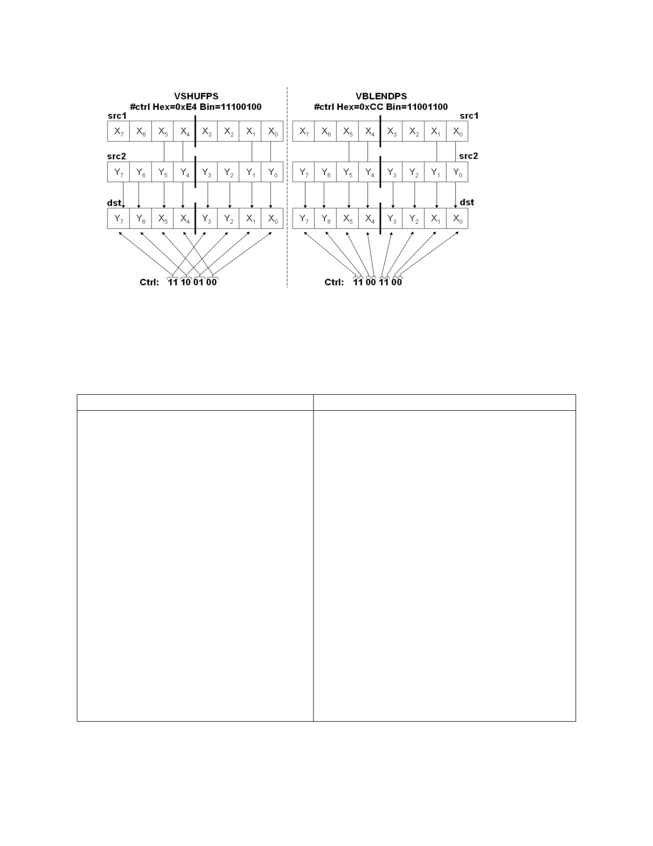
OPTIMIZATIONS FOR INTEL® AVX, INTEL® AVX2, AND INTEL® FMA
The following example shows two implementations of an 8x8 Matrix transpose. In both cases, the bottle-
neck is Port 5 pressure. Alternative 1 uses 12 vshufps instructions that are executed only on port 5. Alter-
native 2 replaces eight of the vshufps instructions with the vblendps instruction which can be executed
on Port 0.
Example 15-19. 8x8 Matrix Transpose - Replace Shuffles with Blends
256-bit AVX using VSHUFPS
AVX replacing VSHUFPS with VBLENDPS
mov rcx, inpBuf
mov rcx, inpBuf
mov rdx, outBuf
mov rdx, outBuf
mov r10, NumOfLoops
mov r10, NumOfLoops
loop1:
loop1:
vmovaps ymm9, [rcx]
vmovaps
ymm9, [rcx]
vmovaps ymm10, [rcx+32]
vmovaps
ymm10, [rcx+32]
vmovaps ymm11, [rcx+64]
vmovaps
ymm11, [rcx+64]
vmovaps ymm12, [rcx+96]
vmovaps
ymm12, [rcx+96]
vmovaps ymm13, [rcx+128]
vmovaps
ymm13, [rcx+128]
vmovaps ymm14, [rcx+160]
vmovaps
ymm14, [rcx+160]
vmovaps ymm15, [rcx+192]
vmovaps
ymm15, [rcx+192]
vmovaps ymm2, [rcx+224]
vmovaps
ymm2, [rcx+224]
vunpcklps ymm6, ymm9, ymm10
vunpcklps
ymm6, ymm9, ymm10
vunpcklps ymm1, ymm11, ymm12
vunpcklps
ymm1, ymm11, ymm12
vunpckhps ymm8, ymm9, ymm10
vunpckhps
ymm8, ymm9, ymm10
vunpcklps ymm0, ymm13, ymm14
vunpcklps
ymm0, ymm13, ymm14
vunpcklps ymm9, ymm15, ymm2
vunpcklps
ymm9, ymm15, ymm2
vshufps
ymm3, ymm6, ymm1, 0x4E
vshufps
ymm3, ymm6, ymm1, 0x4E
vshufps
ymm10, ymm6, ymm3, 0xE4
vblendps
ymm10, ymm6, ymm3, 0xCC
vshufps
ymm6, ymm0, ymm9, 0x4E
vshufps
ymm6, ymm0, ymm9, 0x4E
vunpckhps ymm7, ymm11, ymm12
vunpckhps
ymm7, ymm11, ymm12
vshufps
ymm11, ymm0, ymm6, 0xE4
vblendps
ymm11, ymm0, ymm6, 0xCC
15-31

OPTIMIZATIONS FOR INTEL® AVX, INTEL® AVX2, AND INTEL® FMA
Example 15-19. 8x8 Matrix Transpose - Replace Shuffles with Blends (Contd.)
256-bit AVX using VSHUFPS
AVX replacing VSHUFPS with VBLENDPS
vshufps
ymm12, ymm3, ymm1, 0xE4
vblendps
ymm12, ymm3, ymm1, 0xCC
vperm2f128
ymm3, ymm10, ymm11, 0x20
vperm2f128
ymm3, ymm10, ymm11, 0x20
vmovaps
[rdx], ymm3
vmovaps
[rdx], ymm3
vunpckhps ymm5, ymm13, ymm14
vunpckhps
ymm5, ymm13, ymm14
vshufps
ymm13, ymm6, ymm9, 0xE4
vblendps
ymm13, ymm6, ymm9, 0xCC
vunpckhps ymm4, ymm15, ymm2
vunpckhps
ymm4, ymm15, ymm2
vperm2f128
ymm2, ymm12, ymm13, 0x20
vperm2f128
ymm2, ymm12, ymm13, 0x20
vmovaps
32[rdx], ymm2
vmovaps
32[rdx], ymm2
vshufps
ymm14, ymm8, ymm7, 0x4E
vshufps
ymm14, ymm8, ymm7, 0x4E
vshufps
ymm15, ymm14, ymm7, 0xE4
vblendps
ymm15, ymm14, ymm7, 0xCC
vshufps
ymm7, ymm5, ymm4, 0x4E
vshufps
ymm7, ymm5, ymm4, 0x4E
vshufps
ymm8, ymm8, ymm14, 0xE4
vblendps
ymm8, ymm8, ymm14, 0xCC
vshufps
ymm5, ymm5, ymm7, 0xE4
vblendps
ymm5, ymm5, ymm7, 0xCC
vperm2f128
ymm6, ymm8, ymm5, 0x20
vperm2f128
ymm6, ymm8, ymm5, 0x20
vmovaps
64[rdx], ymm6
vmovaps
64[rdx], ymm6
vshufps
ymm4, ymm7, ymm4, 0xE4
vblendps
ymm4, ymm7, ymm4, 0xCC
vperm2f128
ymm7, ymm15, ymm4, 0x20
vperm2f128
ymm7, ymm15, ymm4, 0x20
vmovaps
96[rdx], ymm7
vmovaps
96[rdx], ymm7
vperm2f128
ymm1, ymm10, ymm11, 0x31
vperm2f128
ymm1, ymm10, ymm11, 0x31
vperm2f128
ymm0, ymm12, ymm13, 0x31
vperm2f128
ymm0, ymm12, ymm13, 0x31
vmovaps
128[rdx], ymm1
vmovaps
128[rdx], ymm1
vperm2f128
ymm5, ymm8, ymm5, 0x31
vperm2f128
ymm5, ymm8, ymm5, 0x31
vperm2f128
ymm4, ymm15, ymm4, 0x31
vperm2f128
ymm4, ymm15, ymm4, 0x31
vmovaps
160[rdx], ymm0
vmovaps
160[rdx], ymm0
vmovaps
192[rdx], ymm5
vmovaps
192[rdx], ymm5
vmovaps
224[rdx], ymm4
vmovaps
224[rdx], ymm4
dec r10
dec
r10
jnz loop1
jnz
loop1
In Example 15-19, replacing VSHUFPS with VBLENDPS relieved port 5 pressure and can gain almost 40%
speedup.
Assembly/Compiler Coding Rule 60. (M impact, M generality) Use Blend instructions in lieu of
shuffle instruction in AVX whenever possible.
15.11.2 Design Algorithm with Fewer Shuffles
In some cases you can reduce port 5 pressure by changing the algorithm to use less shuffles. The figure
below shows that the transpose moved all the elements in rows 0-4 to the low lanes, and all the elements
in rows 4-7 to the high lanes. Therefore, using 256-bit loads in the beginning of the algorithm requires
using VPERM2F128 in order to swap elements between the lanes. The processor executes the
VPERM2F128 instruction only on port 5.
Example 15-19 used eight 256-bit loads and eight VPERM2F128 instructions. You can implement the
same 8x8 Matrix Transpose using VINSERTF128 instead of the 256-bit loads and the eight VPERM2F128.
Using VINSERTF128 from memory is executed in the load ports and on port 0 or 5. The original method
required loads that are performed on the load ports and VPERM2F128 that is only performed on port 5.
Therefore redesigning the algorithm to use VINSERTF128 reduces port 5 pressure and improves perfor-
mance.
15-32
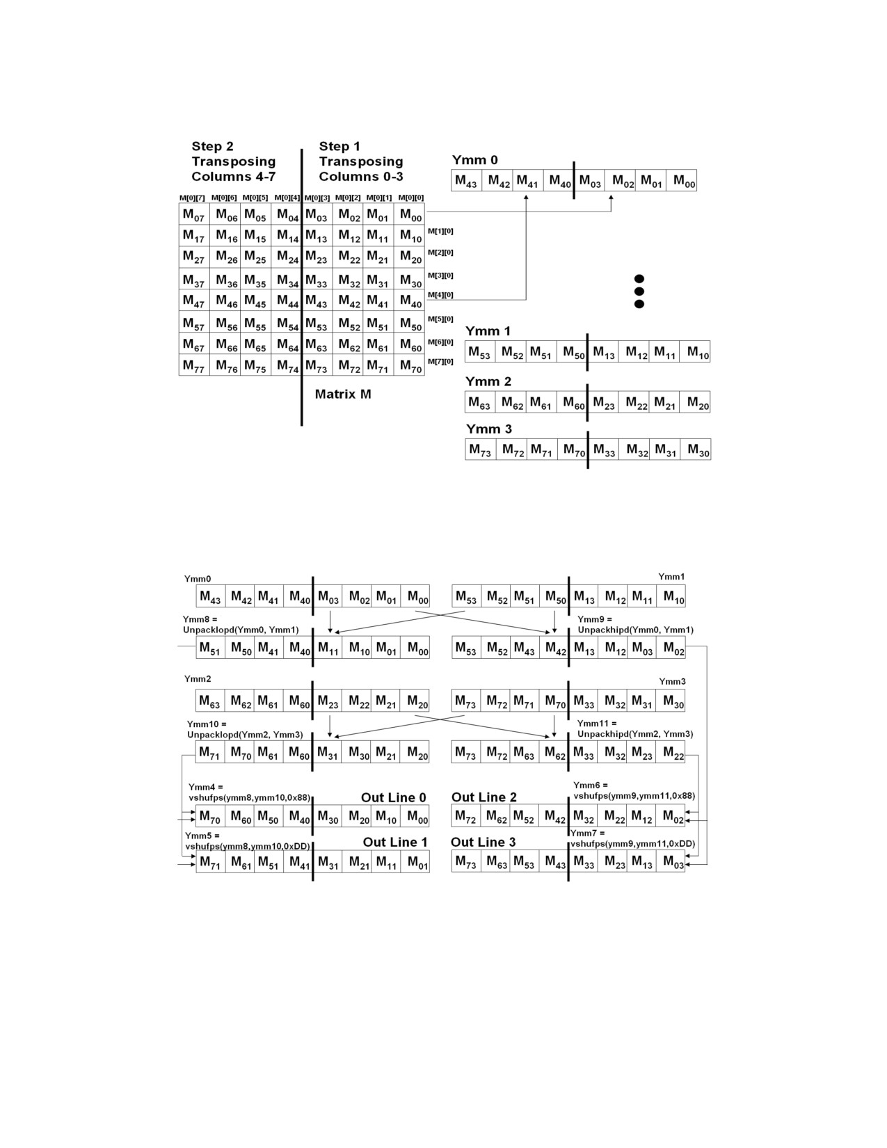
OPTIMIZATIONS FOR INTEL® AVX, INTEL® AVX2, AND INTEL® FMA
The following figure describes step 1 of the 8x8 matrix transpose with vinsertf128. Step 2 performs the
same operations on different columns.
15-33

OPTIMIZATIONS FOR INTEL® AVX, INTEL® AVX2, AND INTEL® FMA
Example 15-20. 8x8 Matrix Transpose Using VINSERTPS
mov
rcx, inpBuf
mov
rdx, outBuf
mov
r10, NumOfLoops
loop1:
vmovaps
xmm0, [rcx]
vinsertf128
ymm0, ymm0, [rcx + 128], 1
vmovaps
xmm1, [rcx + 32]
vinsertf128
ymm1, ymm1, [rcx + 160], 1
vunpcklpd
ymm8, ymm0, ymm1
vunpckhpd
ymm9, ymm0, ymm1
vmovaps
xmm2, [rcx+64]
vinsertf128
ymm2, ymm2, [rcx + 192], 1
vmovaps
xmm3, [rcx+96]
vinsertf128
ymm3, ymm3, [rcx + 224], 1
vunpcklpd
ymm10, ymm2, ymm3
vunpckhpd
ymm11, ymm2, ymm3
vshufps
ymm4, ymm8, ymm10, 0x88
vmovaps
[rdx], ymm4
vshufps
ymm5, ymm8, ymm10, 0xDD
vmovaps
[rdx+32], ymm5
vshufps
ymm6, ymm9, ymm11, 0x88
vmovaps
[rdx+64], ymm6
vshufps
ymm7, ymm9, ymm11, 0xDD
vmovaps
[rdx+96], ymm7
vmovaps
xmm0, [rcx+16]
vinsertf128
ymm0, ymm0, [rcx + 144], 1
vmovaps
xmm1, [rcx + 48]
vinsertf128
ymm1, ymm1, [rcx + 176], 1
vunpcklpd
ymm8, ymm0, ymm1
vunpckhpd
ymm9, ymm0, ymm1
vmovaps
xmm2, [rcx+80]
vinsertf128
ymm2, ymm2, [rcx + 208], 1
vmovaps
xmm3, [rcx+112]
vinsertf128
ymm3, ymm3, [rcx + 240], 1
vunpcklpd
ymm10, ymm2, ymm3
vunpckhpd
ymm11, ymm2, ymm3
vshufps
ymm4, ymm8, ymm10, 0x88
vmovaps
[rdx+128], ymm4
vshufps
ymm5, ymm8, ymm10, 0xDD
vmovaps
[rdx+160], ymm5
vshufps
ymm6, ymm9, ymm11, 0x88
vmovaps
[rdx+192], ymm6
vshufps
ymm7, ymm9, ymm11, 0xDD
vmovaps
[rdx+224], ymm7
dec
r10
jnz
loop1
15-34
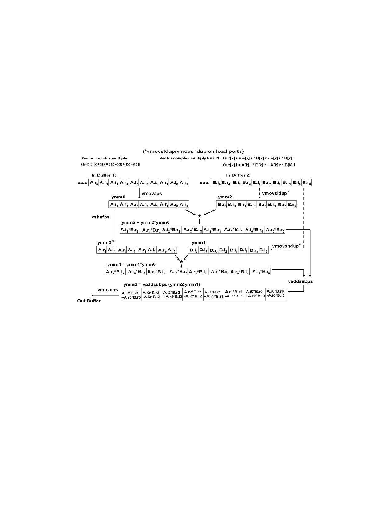
OPTIMIZATIONS FOR INTEL® AVX, INTEL® AVX2, AND INTEL® FMA
In Example 15-20, this reduced port 5 pressure further than the combination of VSHUFPS with
VBLENDPS in Example 15-19. It can gain 70% speedup relative to relying on VSHUFPS alone in Example
15-19.
15.11.3 Perform Basic Shuffles on Load Ports
Some shuffles can be executed in the load ports (ports 2, 3) if the source is from memory. The following
example shows how moving some shuffles (vmovsldup/vmovshdup) from Port 5 to the load ports
improves performance significantly.
The following figure describes an Intel AVX implementation of the complex multiply algorithm with
vmovsldup/vmovshdup on the load ports.
Example 15-21 includes two versions of the complex multiply. Both versions are unrolled twice. Alterna-
tive 1 shuffles all the data in registers. Alternative 2 shuffles data while it is loaded from memory.
15-35

OPTIMIZATIONS FOR INTEL® AVX, INTEL® AVX2, AND INTEL® FMA
Example 15-21. Port 5 versus Load Port Shuffles
Shuffles data in registers
Shuffling loaded data
mov rax, inPtr1
mov rax, inPtr1
mov rbx, inPtr2
mov rbx, inPtr2
mov rdx, outPtr
mov rdx, outPtr
mov r8, len
mov r8, len
xor
rcx, rcx
xor
rcx, rcx
loop1:
loop1:
vmovaps ymm0, [rax +8*rcx]
vmovaps ymm0, [rax +8*rcx]
vmovaps ymm4, [rax +8*rcx +32]
vmovaps ymm4, [rax +8*rcx +32]
vmovaps ymm3, [rbx +8*rcx]
vmovsldup ymm2, ymm3
vmovsldup ymm2, [rbx +8*rcx]
vmulps ymm2, ymm2, ymm0
vmulps ymm2, ymm2, ymm0
vshufps ymm0, ymm0, ymm0, 177
vshufps ymm0, ymm0, ymm0, 177
vmovshdup ymm1, ymm3
vmovshdup ymm1, [rbx +8*rcx]
vmulps ymm1, ymm1, ymm0
vmulps ymm1, ymm1, ymm0
vmovaps ymm7, [rbx +8*rcx +32]
vmovsldup ymm6, [rbx +8*rcx +32]
vmovsldup ymm6, ymm7
vmulps ymm6, ymm6, ymm4
vmulps ymm6, ymm6, ymm4
vaddsubps
ymm3, ymm2, ymm1
vaddsubps
ymm2, ymm2, ymm1
vmovshdup
ymm5, [rbx +8*rcx +32]
vmovshdup
ymm5, ymm7
vmovaps
[rdx+8*rcx], ymm2
vmovaps
[rdx +8*rcx], ymm3
vshufps ymm4, ymm4, ymm4, 177
vshufps ymm4, ymm4, ymm4, 177
vmulps ymm5, ymm5, ymm4
vmulps ymm5, ymm5, ymm4
vaddsubps
ymm6, ymm6, ymm5
vaddsubps ymm7, ymm6, ymm5
vmovaps
[rdx+8*rcx+32], ymm6
vmovaps
[rdx +8*rcx +32], ymm7
add
rcx, 8
add
rcx, 8
cmp
rcx, r8
cmp
rcx, r8
jl
loop1
jl
loop1
15.12 DIVIDE AND SQUARE ROOT OPERATIONS
In Intel microarchitectures prior to Skylake, the SSE divide and square root instructions DIVPS and
SQRTPS have a latency of 14 cycles (or the neighborhood) and they are not pipelined. This means that
the throughput of these instructions is one in every 14 cycles. The 256-bit Intel AVX instructions VDIVPS
and VSQRTPS execute with 128-bit data path and have a latency of 28 cycles and they are not pipelined
as well. Therefore, the performance of the Intel SSE divide and square root instructions is similar to the
Intel AVX 256-bit instructions on Sandy Bridge microarchitecture.
With the Skylake microarchitecture, 256-bit and 128-bit version of (V)DIVPS/(V)SQRTPS have the same
latency because the 256-bit version can execute with a 256-bit data path. The latency is improved and is
pipelined to execute with significantly improved throughput. See Appendix D.3, “Latency and
Throughput”.
In microarchitectures that provide DIVPS/SQRTPS with high latency and low throughput, it is possible to
speed up single-precision divide and square root calculations using the (V)RSQRTPS and (V)RCPPS
instructions. For example, with 128-bit RCPPS/RSQRTPS at 5-cycle latency and 1-cycle throughput or
with 256-bit implementation of these instructions at 7-cycle latency and 2-cycle throughput, a single
Newton-Raphson iteration or Taylor approximation can achieve almost the same precision as the
15-36

OPTIMIZATIONS FOR INTEL® AVX, INTEL® AVX2, AND INTEL® FMA
(V)DIVPS and (V)SQRTPS instructions. See Intel® 64 and IA-32 Architectures Software Developer's
Manual for more information on these instructions.
In some cases, when the divide or square root operations are part of a larger algorithm that hides some
of the latency of these operations, the approximation with Newton-Raphson can slow down execution,
because more micro-ops, coming from the additional instructions, fill the pipe.
With the Skylake microarchitecture, choosing between approximate reciprocal instruction alternative
versus DIVPS/SQRTPS for optimal performance of simple algebraic computations depend on a number of
factors. Table 15-5 shows several algebraic formula the throughput comparison of implementations of
different numeric accuracy tolerances. In each row, 24-bit accurate implementations are IEEE-compliant
and using the respective instructions of 128-bit or 256-bit ISA. The columns of 22-bit and 11-bit accurate
implementations are using approximate reciprocal instructions of the respective instruction set.
Table 15-5. Comparison of Numeric Alternatives of Selected Linear Algebra in Skylake Microarchitecture
Algorithm
Instruction Type
24-bit Accurate
22-bit Accurate
11-bit Accurate
Z = X/Y
SSE
1X
0.9X
1.3X
256-bit AVX
1X
1.5X
2.6X
Z = X0.5
SSE
1X
0.7X
2X
256-bit AVX
1X
1.4X
3.4X
Z = X-0.5
SSE
1X
1.7X
4.3X
256-bit AVX
1X
3X
7.7X
Z = (X *Y + Y*Y )0.5
SSE
1X
0.75X
0.85X
256-bit AVX
1X
1.1X
1.6X
Z = (X+2Y+3)/(Z-2Y-3)
SSE
1X
0.85X
1X
256-bit AVX
1X
0.8X
1X
If targeting processors based on the Skylake microarchitecture, Table 15-5 can be summarized as:
• For 256- bit AVX code, Newton-Raphson approximation can be beneficial on Skylake microarchi-
tecture when the algorithm contains only operations executed on the divide unit. However, when
single precision divide or square root operations are part of a longer computation, the lower latency
of the DIVPS or SQRTPS instructions can lead to better overall performance.
• For SSE or 128-bit AVX implementation, consider use of approximation for divide and square root
instructions only for algorithms that do not require precision higher than 11-bit or algorithms that
contain multiple operations executed on the divide unit.
Table 15-6 summarizes recommended calculation methods of divisions or square root when using single-
precision instructions, based on the desired accuracy level across recent generations of Intel microarchi-
tectures.
Table 15-6. Single-Precision Divide and Square Root Alternatives
Operation
Accuracy Tolerance
Recommendation
Divide
24 bits (IEEE)
DIVPS
~ 22 bits
Skylake: Consult Table 15-5
Prior uarch: RCPPS + 1 Newton-Raphson Iteration + MULPS
~ 11 bits
RCPPS + MULPS
Reciprocal square
24 bits (IEEE)
SQRTPS + DIVPS
root
~ 22 bits
RSQRTPS + 1 Newton-Raphson Iteration
~ 11 bits
RSQRTPS
15-37

OPTIMIZATIONS FOR INTEL® AVX, INTEL® AVX2, AND INTEL® FMA
Table 15-6. Single-Precision Divide and Square Root Alternatives (Contd.)
Operation
Accuracy Tolerance
Recommendation
Square root
24 bits (IEEE)
SQRTPS
~ 22 bits
Skylake: Consult Table 15-5
Prior uarch: RSQRTPS + 1 Newton-Raphson Iteration + MULPS
~ 11 bits
RSQRTPS + RCPPS
15.12.1 Single-Precision Divide
To compute:
Z[i]=A[i]/B[i]
On a large vector of single-precision numbers, Z[i] can be calculated by a divide operation, or by multi-
plying 1/B[i] by A[i].
Denoting B[i] by N, it is possible to calculate 1/N using the (V)RCPPS instruction, achieving approxi-
mately 11-bit precision.
For better accuracy you can use the one Newton-Raphson iteration:
X_(0 ) ~= 1/N
; Initial estimation, rcp(N)
X_(0 ) = 1/N*(1-E)
E=1-N*X_0
; E ~= 2^(-11)
X_1=X_0*(1+E)=1/N*(1-E^2 )
; E^2 ~= 2^(-22)
X_1=X_0*(1+1-N*X_0 )= 2 *X_0 - N*X_0^2
X_1 is an approximation of 1/N with approximately 22-bit precision.
Example 15-22. Divide Using DIVPS for 24-bit Accuracy
SSE code using DIVPS
Using VDIVPS
mov rax, pIn1
mov rax, pIn1
mov rbx, pIn2
mov rbx, pIn2
mov rcx, pOut
mov rcx, pOut
mov rsi, iLen
mov rsi, iLen
xor rdx, rdx
xor rdx, rdx
loop1:
loop1:
movups xmm0, [rax+rdx*1]
vmovups ymm0, [rax+rdx*1]
movups xmm1, [rbx+rdx*1]
vmovups ymm1, [rbx+rdx*1]
divps xmm0, xmm1
vdivps ymm0, ymm0, ymm1
movups [rcx+rdx*1], xmm0
vmovups [rcx+rdx*1], ymm0
add rdx, 16
add rdx, 32
cmp rdx, rsi
cmp rdx, rsi
jl loop1
jl loop1
15-38

OPTIMIZATIONS FOR INTEL® AVX, INTEL® AVX2, AND INTEL® FMA
Example 15-23. Divide Using RCPPS 11-bit Approximation
SSE code using RCPPS
Using VRCPPS
mov rax, pIn1
mov rax, pIn1
mov rbx, pIn2
mov rbx, pIn2
mov rcx, pOut
mov rcx, pOut
mov rsi, iLen
mov rsi, iLen
xor rdx, rdx
xor rdx, rdx
loop1:
loop1:
movups xmm0,[rax+rdx*1]
vmovups ymm0, [rax+rdx]
movups xmm1,[rbx+rdx*1]
vmovups ymm1, [rbx+rdx]
rcpps xmm1,xmm1
vrcpps ymm1, ymm1
mulps xmm0,xmm1
vmulps ymm0, ymm0, ymm1
movups [rcx+rdx*1],xmm0
vmovups [rcx+rdx], ymm0
add rdx, 16
add rdx, 32
cmp rdx, rsi
cmp rdx, rsi
jl loop1
jl loop1
Example 15-24. Divide Using RCPPS and Newton-Raphson Iteration
RCPPS + MULPS ~ 22 bit accuracy
VRCPPS + VMULPS ~ 22 bit accuracy
mov rax, pIn1
mov rax, pIn1
mov rbx, pIn2
mov rbx, pIn2
mov rcx, pOut
mov rcx, pOut
mov rsi, iLen
mov rsi, iLen
xor rdx, rdx
xor rdx, rdx
loop1:
loop1:
movups xmm0, [rax+rdx*1]
vmovups ymm0, [rax+rdx]
movups xmm1, [rbx+rdx*1]
vmovups ymm1, [rbx+rdx]
rcpps xmm3, xmm1
vrcpps ymm3, ymm1
movaps xmm2, xmm3
addps xmm3, xmm2
vaddps ymm2, ymm3, ymm3
mulps xmm2, xmm2
vmulps ymm3, ymm3, ymm3
mulps xmm2, xmm1
vmulps ymm3, ymm3, ymm1
subps xmm3, xmm2
vsubps ymm2, ymm2, ymm3
mulps xmm0, xmm3
vmulps ymm0, ymm0, ymm2
movups [rcx+rdx*1], xmm0
vmovups [rcx+rdx], ymm0
add rdx, 16
add rdx, 32
cmp rdx, rsi
cmp rdx, rsi
jl loop1
jl loop1
15.12.2 Single-Precision Reciprocal Square Root
To compute Z[i]=1/ (A[i]) ^0.5 on a large vector of single-precision numbers, denoting A[i] by N, it is
possible to calculate 1/N using the (V)RSQRTPS instruction.
For better accuracy you can use one Newton-Raphson iteration:
15-39

OPTIMIZATIONS FOR INTEL® AVX, INTEL® AVX2, AND INTEL® FMA
X_0 ~=1/N ; Initial estimation RCP(N)
E=1-N*X_0^2
X_0= (1/N)^0.5 * ((1-E)^0.5 ) = (1/N)^0.5 * (1-E/2) ; E/2~= 2^(-11)
X_1=X_0*(1+E/2) ~= (1/N)^0.5 * (1-E^2/4)
; E^2/4?2^(-22)
X_1=X_0*(1+1/2-1/2*N*X_0^2 )= 1/2*X_0*(3-N*X_0^2)
X1 is an approximation of (1/N)^0.5 with approximately 22-bit precision.
Example 15-25. Reciprocal Square Root Using DIVPS+SQRTPS for 24-bit Accuracy
Using SQRTPS, DIVPS
Using VSQRTPS, VDIVPS
mov rax, pIn
mov rax, pIn
mov rbx, pOut
mov rbx, pOut
mov rcx, iLen
mov rcx, iLen
xor rdx, rdx
xor rdx, rdx
loop1:
loop1:
movups xmm1, [rax+rdx]
vmovups ymm1, [rax+rdx]
sqrtps xmm0, xmm1
vsqrtps ymm0, ymm1
divps xmm0, xmm1
vdivps ymm0, ymm0, ymm1
movups [rbx+rdx], xmm0
vmovups [rbx+rdx], ymm0
add rdx, 16
add rdx, 32
cmp rdx, rcx
cmp rdx, rcx
jl loop1
jl loop1
Example 15-26. Reciprocal Square Root Using RSQRTPS 11-bit Approximation
SSE code using RSQRTPS
Using VRSQRTPS
mov rax, pIn
mov rax, pIn
mov rbx, pOut
mov rbx, pOut
mov rcx, iLen
mov rcx, iLen
xor rdx, rdx
xor rdx, rdx
loop1:
rsqrtps xmm0, [rax+rdx]
loop1:
movups [rbx+rdx], xmm0
vrsqrtps ymm0, [rax+rdx]
add rdx, 16
vmovups [rbx+rdx], ymm0
cmp rdx, rcx
add rdx, 32
jl loop1
cmp rdx, rcx
jl loop1
15-40

OPTIMIZATIONS FOR INTEL® AVX, INTEL® AVX2, AND INTEL® FMA
Example 15-27. Reciprocal Square Root Using RSQRTPS and Newton-Raphson Iteration
RSQRTPS + MULPS ~ 22 bit accuracy
VRSQRTPS + VMULPS ~ 22 bit accuracy
__declspec(align(16)) float minus_half[4] = {-0.5, -0.5, -
__declspec(align(32)) float half[8] =
0.5, -0.5};
{0.5, 0.5, 0.5, 0.5, 0.5, 0.5, 0.5, 0.5};
__declspec(align(16)) float three[4] = {3.0, 3.0, 3.0,
__declspec(align(32)) float three[8] =
3.0};
{3.0, 3.0, 3.0, 3.0, 3.0, 3.0, 3.0, 3.0};
__asm
__asm
{
{
mov rax, pIn
mov rax, pIn
mov rbx, pOut
mov rbx, pOut
mov rcx, iLen
mov rcx, iLen
xor rdx, rdx
xor rdx, rdx
movups xmm3, [three]
vmovups ymm3, [three]
movups xmm4, [minus_half]
vmovups ymm4, [half]
loop1:
loop1:
movups xmm5, [rax+rdx]
vmovups ymm5, [rax+rdx]
rsqrtps xmm0, xmm5
vrsqrtps ymm0, ymm5
movaps xmm2, xmm0
mulps xmm0, xmm0
vmulps ymm2, ymm0, ymm0
mulps xmm0, xmm5
vmulps ymm2, ymm2, ymm5
subps xmm0, xmm3
vsubps ymm2, ymm3, ymm2
mulps xmm0, xmm2
vmulps ymm0, ymm0, ymm2
mulps xmm0, xmm4
vmulps ymm0, ymm0, ymm4
movups [rbx+rdx], xmm0
add rdx, 16
vmovups [rbx+rdx], ymm0
cmp rdx, rcx
add rdx, 32
jl loop1
cmp rdx, rcx
}
jl loop1
}
15.12.3 Single-Precision Square Root
To compute Z[i]= (A[i])^0.5 on a large vector of single-precision numbers, denoting A[i] by N, the
approximation for N^0.5 is N multiplied by (1/N)^0.5 , where the approximation for (1/N)^0.5 is
described in the previous section.
To get approximately 22-bit precision of N^0.5, use the following calculation:
N^0.5 = X_1*N = 1/2*N*X_0*(3-N*X_0^2)
15-41

OPTIMIZATIONS FOR INTEL® AVX, INTEL® AVX2, AND INTEL® FMA
Example 15-28. Square Root Using SQRTPS for 24-bit Accuracy
Using SQRTPS
Using VSQRTPS
mov rax, pIn
mov rax, pIn
mov rbx, pOut
mov rbx, pOut
mov rcx, iLen
mov rcx, iLen
xor rdx, rdx
xor rdx, rdx
loop1:
loop1:
movups xmm1, [rax+rdx]
vmovups ymm1, [rax+rdx]
sqrtps xmm1, xmm1
vsqrtps ymm1,ymm1
movups [rbx+rdx], xmm1
vmovups [rbx+rdx], ymm1
add rdx, 16
add rdx, 32
cmp rdx, rcx
cmp rdx, rcx
jl loop1
jl loop1
Example 15-29. Square Root Using RSQRTPS 11-bit Approximation
SSE code using RSQRTPS
Using VRSQRTPS
mov rax, pIn
mov rax, pIn
mov rbx, pOut
mov rbx, pOut
mov rcx, iLen
mov rcx, iLen
xor rdx, rdx
xor rdx, rdx
loop1:
vxorps ymm8, ymm8, ymm8
movups xmm1, [rax+rdx]
loop1:
xorps xmm8, xmm8
vmovups ymm1, [rax+rdx]
cmpneqps xmm8, xmm1
vcmpneqps ymm9, ymm8, ymm1
rsqrtps xmm1, xmm1
vrsqrtps ymm1, ymm1
rcpps xmm1, xmm1
vrcpps ymm1, ymm1
andps xmm1, xmm8
vandps ymm1, ymm1, ymm9
movups [rbx+rdx], xmm1
vmovups [rbx+rdx], ymm1
add rdx, 16
add rdx, 32
cmp rdx, rcx
cmp rdx, rcx
jl loop1
jl loop1
15-42

OPTIMIZATIONS FOR INTEL® AVX, INTEL® AVX2, AND INTEL® FMA
Example 15-30. Square Root Using RSQRTPS and One Taylor Series Expansion
RSQRTPS + Taylor ~ 22 bit accuracy
VRSQRTPS + Taylor ~ 22 bit accuracy
__declspec(align(16)) float minus_half[4] =
__declspec(align(32)) float three[8] =
{-0.5, -0.5, -0.5, -0.5};
{3.0, 3.0, 3.0, 3.0, 3.0, 3.0, 3.0, 3.0};
__declspec(align(16)) float three[4] =
__declspec(align(32)) float minus_half[8] =
{3.0, 3.0, 3.0, 3.0};
{-0.5, -0.5, -0.5, -0.5, -0.5, -0.5, -0.5, -0.5};
__asm
__asm
{
{
mov rax, pIn
mov rax, pIn
mov rbx, pOut
mov rbx, pOut
mov rcx, iLen
mov rcx, iLen
xor rdx, rdx
xor rdx, rdx
movups xmm6, [three]
vmovups ymm6, [three]
movups xmm7, [minus_half]
vmovups ymm7, [minus_half]
loop1:
vxorps ymm8, ymm8, ymm8
movups xmm3, [rax+rdx]
loop1:
rsqrtps xmm1, xmm3
vmovups ymm3, [rax+rdx]
xorps xmm8, xmm8
vrsqrtps ymm4, ymm3
cmpneqps xmm8, xmm3
vcmpneqps ymm9, ymm8, ymm3
andps xmm1, xmm8
vandps ymm4, ymm4, ymm9
movaps xmm4, xmm1
vmulps ymm1, ymm4, ymm3
mulps xmm1, xmm3
vmulps ymm2, ymm1, ymm4
movaps xmm5, xmm1
vsubps ymm2, ymm2, ymm6
mulps xmm1, xmm4
vmulps ymm1, ymm1, ymm2
subps xmm1, xmm6
vmulps ymm1, ymm1, ymm7
mulps xmm1, xmm5
vmovups [rbx+rdx], ymm1
mulps xmm1, xmm7
add rdx, 32
movups [rbx+rdx], xmm1
cmp rdx, rcx
add rdx, 16
jl loop1
cmp rdx, rcx
}
jl loop1
}
15.13 OPTIMIZATION OF ARRAY SUB SUM EXAMPLE
This section shows the transformation of SSE implementation of Array Sub Sum algorithm to Intel AVX
implementation.
The Array Sub Sum algorithm is:
Y[i] = Sum of k from 0 to i ( X[k]) = X[0] + X[1] + .. + X[i]
The following figure describes the SSE implementation.
15-43