Intel 64 and IA-32 Architectures. Software Developer’s Manual (Collection, 2023) - page 123
INSTRUCTION SET REFERENCE UNIQUE TO INTEL® XEON PHI™ PROCESSORS
VSCATTERPF0DPS (EVEX Encoded Version)
(KL, VL) = (16, 512)
FOR j := 0 TO KL-1
i := j * 32
IF k1[j]
Prefetch( [BASE_ADDR + SignExtend(VINDEX[i+31:i]) * SCALE + DISP], Level=0, RFO = 1)
FI;
ENDFOR
VSCATTERPF0DPD (EVEX Encoded Version)
(KL, VL) = (8, 512)
FOR j := 0 TO KL-1
i := j * 64
k := j * 32
IF k1[j]
Prefetch( [BASE_ADDR + SignExtend(VINDEX[k+31:k]) * SCALE + DISP], Level=0, RFO = 1)
FI;
ENDFOR
VSCATTERPF0QPS (EVEX Encoded Version)
(KL, VL) = (8, 256)
FOR j := 0 TO KL-1
i := j * 64
IF k1[j]
Prefetch( [BASE_ADDR + SignExtend(VINDEX[i+63:i]) * SCALE + DISP], Level=0, RFO = 1)
FI;
ENDFOR
VSCATTERPF0QPD (EVEX Encoded Version)
(KL, VL) = (8, 512)
FOR j := 0 TO KL-1
i := j * 64
k := j * 64
IF k1[j]
Prefetch( [BASE_ADDR + SignExtend(VINDEX[k+63:k]) * SCALE + DISP], Level=0, RFO = 1)
FI;
ENDFOR
Intel C/C++ Compiler Intrinsic Equivalent
VSCATTERPF0DPD void _mm512_prefetch_i32scatter_pd(void *base, __m256i vdx, int scale, int hint);
VSCATTERPF0DPD void _mm512_mask_prefetch_i32scatter_pd(void *base, __mmask8 m, __m256i vdx, int scale, int hint);
VSCATTERPF0DPS void _mm512_prefetch_i32scatter_ps(void *base, __m512i vdx, int scale, int hint);
VSCATTERPF0DPS void _mm512_mask_prefetch_i32scatter_ps(void *base, __mmask16 m, __m512i vdx, int scale, int hint);
VSCATTERPF0QPD void _mm512_prefetch_i64scatter_pd(void * base, __m512i vdx, int scale, int hint);
VSCATTERPF0QPD void _mm512_mask_prefetch_i64scatter_pd(void * base, __mmask8 m, __m512i vdx, int scale, int hint);
VSCATTERPF0QPS void _mm512_prefetch_i64scatter_ps(void * base, __m512i vdx, int scale, int hint);
VSCATTERPF0QPS void _mm512_mask_prefetch_i64scatter_ps(void * base, __mmask8 m, __m512i vdx, int scale, int hint);
SIMD Floating-Point Exceptions
None.
Other Exceptions
See Table 2-62, “Type E12NP Class Exception Conditions.”
VSCATTERPF0DPS/VSCATTERPF0QPS/VSCATTERPF0DPD/VSCATTERPF0QPD—Sparse Prefetch Packed SP/DP Data Values with
Vol. 2D
8-37

INSTRUCTION SET REFERENCE UNIQUE TO INTEL® XEON PHI™ PROCESSORS
VSCATTERPF1DPS/VSCATTERPF1QPS/VSCATTERPF1DPD/VSCATTERPF1QPD—Sparse Prefetch
Packed SP/DP Data Values With Signed Dword, Signed Qword Indices Using T1 Hint With Intent
to Write
Opcode/
Op/
64/32
CPUID
Description
Instruction
En
bit Mode
Feature
Support
Flag
EVEX.512.66.0F38.W0 C6 /6 /vsib
A
V/V
AVX512PF
Using signed dword indices, prefetch sparse byte memory
VSCATTERPF1DPS vm32z {k1}
locations containing single-precision data using writemask
k1 and T1 hint with intent to write.
EVEX.512.66.0F38.W0 C7 /6 /vsib
A
V/V
AVX512PF
Using signed qword indices, prefetch sparse byte memory
VSCATTERPF1QPS vm64z {k1}
locations containing single-precision data using writemask
k1 and T1 hint with intent to write.
EVEX.512.66.0F38.W1 C6 /6 /vsib
A
V/V
AVX512PF
Using signed dword indices, prefetch sparse byte memory
VSCATTERPF1DPD vm32y {k1}
locations containing double precision data using
writemask k1 and T1 hint with intent to write.
EVEX.512.66.0F38.W1 C7 /6 /vsib
A
V/V
AVX512PF
Using signed qword indices, prefetch sparse byte memory
VSCATTERPF1QPD vm64z {k1}
locations containing double precision data using
writemask k1 and T1 hint with intent to write.
Instruction Operand Encoding
Op/En
Tuple Type
Operand 1
Operand 2
Operand 3
Operand 4
A
Tuple1 Scalar
BaseReg (R): VSIB:base,
N/A
N/A
N/A
VectorReg(R): VSIB:index
Description
The instruction conditionally prefetches up to sixteen 32-bit or eight 64-bit integer byte data elements. The
elements are specified via the VSIB (i.e., the index register is an zmm, holding packed indices). Elements will only
be prefetched if their corresponding mask bit is one.
cache lines will be brought into exclusive state (RFO) specified by a locality hint (T1):
• T1 (temporal data)—prefetch data into the second level cache.
[PS data] For dword indices, the instruction will prefetch sixteen memory locations. For qword indices, the instruc-
tion will prefetch eight values.
[PD data] For dword and qword indices, the instruction will prefetch eight memory locations.
Note that:
(1) The prefetches may happen in any order (or not at all). The instruction is a hint.
(2) The mask is left unchanged.
(3) Not valid with 16-bit effective addresses. Will deliver a #UD fault.
(4) No FP nor memory faults may be produced by this instruction.
(5) Prefetches do not handle cache line splits
(6) A #UD is signaled if the memory operand is encoded without the SIB byte.
Operation
BASE_ADDR stands for the memory operand base address (a GPR); may not exist.
VINDEX stands for the memory operand vector of indices (a vector register).
SCALE stands for the memory operand scalar (1, 2, 4 or 8).
DISP is the optional 1, 2 or 4 byte displacement.
PREFETCH(mem, Level, State) Prefetches a byte memory location pointed by ‘mem’ into the cache level specified by ‘Level’; a request
for exclusive/ownership is done if ‘State’ is 1. Note that the memory location ignore cache line splits. This operation is considered a
hint for the processor and may be skipped depending on implementation.
VSCATTERPF1DPS/VSCATTERPF1QPS/VSCATTERPF1DPD/VSCATTERPF1QPD—Sparse Prefetch Packed SP/DP Data Values With
8-38
Vol. 2D
INSTRUCTION SET REFERENCE UNIQUE TO INTEL® XEON PHI™ PROCESSORS
VSCATTERPF1DPS (EVEX Encoded Version)
(KL, VL) = (16, 512)
FOR j := 0 TO KL-1
i := j * 32
IF k1[j]
Prefetch( [BASE_ADDR + SignExtend(VINDEX[i+31:i]) * SCALE + DISP], Level=1, RFO = 1)
FI;
ENDFOR
VSCATTERPF1DPD (EVEX Encoded Version)
(KL, VL) = (8, 512)
FOR j := 0 TO KL-1
i := j * 64
k := j * 32
IF k1[j]
Prefetch( [BASE_ADDR + SignExtend(VINDEX[k+31:k]) * SCALE + DISP], Level=1, RFO = 1)
FI;
ENDFOR
VSCATTERPF1QPS (EVEX Encoded Version)
(KL, VL) = (8, 512)
FOR j := 0 TO KL-1
i := j * 64
IF k1[j]
Prefetch( [BASE_ADDR + SignExtend(VINDEX[i+63:i]) * SCALE + DISP], Level=1, RFO = 1)
FI;
ENDFOR
VSCATTERPF1QPD (EVEX Encoded Version)
(KL, VL) = (8, 512)
FOR j := 0 TO KL-1
i := j * 64
k := j * 64
IF k1[j]
Prefetch( [BASE_ADDR + SignExtend(VINDEX[k+63:k]) * SCALE + DISP], Level=1, RFO = 1)
FI;
ENDFOR
Intel C/C++ Compiler Intrinsic Equivalent
VSCATTERPF1DPD void _mm512_prefetch_i32scatter_pd(void *base, __m256i vdx, int scale, int hint);
VSCATTERPF1DPD void _mm512_mask_prefetch_i32scatter_pd(void *base, __mmask8 m, __m256i vdx, int scale, int hint);
VSCATTERPF1DPS void _mm512_prefetch_i32scatter_ps(void *base, __m512i vdx, int scale, int hint);
VSCATTERPF1DPS void _mm512_mask_prefetch_i32scatter_ps(void *base, __mmask16 m, __m512i vdx, int scale, int hint);
VSCATTERPF1QPD void _mm512_prefetch_i64scatter_pd(void * base, __m512i vdx, int scale, int hint);
VSCATTERPF1QPD void _mm512_mask_prefetch_i64scatter_pd(void * base, __mmask8 m, __m512i vdx, int scale, int hint);
VSCATTERPF1QPS void _mm512_prefetch_i64scatter_ps(void *base, __m512i vdx, int scale, int hint);
VSCATTERPF1QPS void _mm512_mask_prefetch_i64scatter_ps(void *base, __mmask8 m, __m512i vdx, int scale, int hint);
SIMD Floating-Point Exceptions
None.
Other Exceptions
See Table 2-62, “Type E12NP Class Exception Conditions.”
VSCATTERPF1DPS/VSCATTERPF1QPS/VSCATTERPF1DPD/VSCATTERPF1QPD—Sparse Prefetch Packed SP/DP Data Values With
Vol. 2D
8-39
INSTRUCTION SET REFERENCE UNIQUE TO INTEL® XEON PHI™ PROCESSORS
VSCATTERPF1DPS/VSCATTERPF1QPS/VSCATTERPF1DPD/VSCATTERPF1QPD—Sparse Prefetch Packed SP/DP Data Values With
8-40
Vol. 2D

APPENDIX A
OPCODE MAP
Use the opcode tables in this chapter to interpret IA-32 and Intel 64 architecture object code. Instructions are
divided into encoding groups:
•
1-byte, 2-byte and 3-byte opcode encodings are used to encode integer, system, MMX technology,
SSE/SSE2/SSE3/SSSE3/SSE4, and VMX instructions. Maps for these instructions are given in Table A-2
through Table A-6.
• Escape opcodes (in the format: ESC character, opcode, ModR/M byte) are used for floating-point instructions.
The maps for these instructions are provided in Table A-7 through Table A-22.
NOTE
All blanks in opcode maps are reserved and must not be used. Do not depend on the operation of
undefined or blank opcodes.
A.1
USING OPCODE TABLES
Tables in this appendix list opcodes of instructions (including required instruction prefixes, opcode extensions in
associated ModR/M byte). Blank cells in the tables indicate opcodes that are reserved or undefined. Cells marked
“Reserved-NOP” are also reserved but may behave as NOP on certain processors. Software should not use opcodes
corresponding blank cells or cells marked “Reserved-NOP” nor depend on the current behavior of those opcodes.
The opcode map tables are organized by hex values of the upper and lower 4 bits of an opcode byte. For 1-byte
encodings (Table A-2), use the four high-order bits of an opcode to index a row of the opcode table; use the four
low-order bits to index a column of the table. For 2-byte opcodes beginning with 0FH (Table A-3), skip any instruc-
tion prefixes, the 0FH byte (0FH may be preceded by 66H, F2H, or F3H) and use the upper and lower 4-bit values
of the next opcode byte to index table rows and columns. Similarly, for 3-byte opcodes beginning with 0F38H or
0F3AH (Table A-4), skip any instruction prefixes, 0F38H or 0F3AH and use the upper and lower 4-bit values of the
third opcode byte to index table rows and columns. See Section A.2.4, “Opcode Look-up Examples for One, Two,
and Three-Byte Opcodes.”
When a ModR/M byte provides opcode extensions, this information qualifies opcode execution. For information on
how an opcode extension in the ModR/M byte modifies the opcode map in Table A-2 and Table A-3, see Section A.4.
The escape (ESC) opcode tables for floating-point instructions identify the eight high order bits of opcodes at the
top of each page. See Section A.5. If the accompanying ModR/M byte is in the range of 00H-BFH, bits 3-5 (the top
row of the third table on each page) along with the reg bits of ModR/M determine the opcode. ModR/M bytes
outside the range of 00H-BFH are mapped by the bottom two tables on each page of the section.
A.2
KEY TO ABBREVIATIONS
Operands are identified by a two-character code of the form Zz. The first character, an uppercase letter, specifies
the addressing method; the second character, a lowercase letter, specifies the type of operand.
A.2.1
Codes for Addressing Method
The following abbreviations are used to document addressing methods:
A
Direct address: the instruction has no ModR/M byte; the address of the operand is encoded in the instruc-
tion. No base register, index register, or scaling factor can be applied (for example, far JMP (EA)).
B
The VEX.vvvv field of the VEX prefix selects a general purpose register.
Vol. 2D A-1
OPCODE MAP
C
The reg field of the ModR/M byte selects a control register (for example, MOV (0F20, 0F22)).
D
The reg field of the ModR/M byte selects a debug register (for example,
MOV (0F21,0F23)).
E
A ModR/M byte follows the opcode and specifies the operand. The operand is either a general-purpose
register or a memory address. If it is a memory address, the address is computed from a segment register
and any of the following values: a base register, an index register, a scaling factor, a displacement.
F
EFLAGS/RFLAGS Register.
G
The reg field of the ModR/M byte selects a general register (for example, AX (000)).
H
The VEX.vvvv field of the VEX prefix selects a 128-bit XMM register or a 256-bit YMM register, determined
by operand type. For legacy SSE encodings this operand does not exist, changing the instruction to
destructive form.
I
Immediate data: the operand value is encoded in subsequent bytes of the instruction.
J
The instruction contains a relative offset to be added to the instruction pointer register (for example, JMP
(0E9), LOOP).
L
The upper 4 bits of the 8-bit immediate selects a 128-bit XMM register or a 256-bit YMM register, deter-
mined by operand type. (the MSB is ignored in 32-bit mode)
M
The ModR/M byte may refer only to memory (for example, BOUND, LES, LDS, LSS, LFS, LGS,
CMPXCHG8B).
N
The R/M field of the ModR/M byte selects a packed-quadword, MMX technology register.
O
The instruction has no ModR/M byte. The offset of the operand is coded as a word or double word
(depending on address size attribute) in the instruction. No base register, index register, or scaling factor
can be applied (for example, MOV (A0-A3)).
P
The reg field of the ModR/M byte selects a packed quadword MMX technology register.
Q
A ModR/M byte follows the opcode and specifies the operand. The operand is either an MMX technology
register or a memory address. If it is a memory address, the address is computed from a segment register
and any of the following values: a base register, an index register, a scaling factor, and a displacement.
R
The R/M field of the ModR/M byte may refer only to a general register (for example, MOV (0F20-0F23)).
S
The reg field of the ModR/M byte selects a segment register (for example, MOV (8C,8E)).
U
The R/M field of the ModR/M byte selects a 128-bit XMM register or a 256-bit YMM register, determined by
operand type.
V
The reg field of the ModR/M byte selects a 128-bit XMM register or a 256-bit YMM register, determined by
operand type.
W
A ModR/M byte follows the opcode and specifies the operand. The operand is either a 128-bit XMM register,
a 256-bit YMM register (determined by operand type), or a memory address. If it is a memory address, the
address is computed from a segment register and any of the following values: a base register, an index
register, a scaling factor, and a displacement.
X
Memory addressed by the DS:rSI register pair (for example, MOVS, CMPS, OUTS, or LODS).
Y
Memory addressed by the ES:rDI register pair (for example, MOVS, CMPS, INS, STOS, or SCAS).
A.2.2
Codes for Operand Type
The following abbreviations are used to document operand types:
a
Two one-word operands in memory or two double-word operands in memory, depending on operand-size
attribute (used only by the BOUND instruction).
b
Byte, regardless of operand-size attribute.
c
Byte or word, depending on operand-size attribute.
d
Doubleword, regardless of operand-size attribute.
A-2
Vol. 2D
OPCODE MAP
dq
Double-quadword, regardless of operand-size attribute.
p
32-bit, 48-bit, or 80-bit pointer, depending on operand-size attribute.
pd
128-bit or 256-bit packed double precision floating-point data.
pi
Quadword MMX technology register (for example: mm0).
ps
128-bit or 256-bit packed single-precision floating-point data.
q
Quadword, regardless of operand-size attribute.
qq
Quad-Quadword (256-bits), regardless of operand-size attribute.
s
6-byte or 10-byte pseudo-descriptor.
sd
Scalar element of a 128-bit double precision floating data.
ss
Scalar element of a 128-bit single-precision floating data.
si
Doubleword integer register (for example: eax).
v
Word, doubleword or quadword (in 64-bit mode), depending on operand-size attribute.
w
Word, regardless of operand-size attribute.
x
dq or qq based on the operand-size attribute.
y
Doubleword or quadword (in 64-bit mode), depending on operand-size attribute.
z
Word for 16-bit operand-size or doubleword for 32 or 64-bit operand-size.
A.2.3
Register Codes
When an opcode requires a specific register as an operand, the register is identified by name (for example, AX, CL,
or ESI). The name indicates whether the register is 64, 32, 16, or 8 bits wide.
A register identifier of the form eXX or rXX is used when register width depends on the operand-size attribute. eXX
is used when 16 or 32-bit sizes are possible; rXX is used when 16, 32, or 64-bit sizes are possible. For example:
eAX indicates that the AX register is used when the operand-size attribute is 16 and the EAX register is used when
the operand-size attribute is 32. rAX can indicate AX, EAX or RAX.
When the REX.B bit is used to modify the register specified in the reg field of the opcode, this fact is indicated by
adding “/x” to the register name to indicate the additional possibility. For example, rCX/r9 is used to indicate that
the register could either be rCX or r9. Note that the size of r9 in this case is determined by the operand size attri-
bute (just as for rCX).
A.2.4
Opcode Look-up Examples for One, Two, and Three-Byte Opcodes
This section provides examples that demonstrate how opcode maps are used.
A.2.4.1
One-Byte Opcode Instructions
The opcode map for 1-byte opcodes is shown in Table A-2. The opcode map for 1-byte opcodes is arranged by row
(the least-significant 4 bits of the hexadecimal value) and column (the most-significant 4 bits of the hexadecimal
value). Each entry in the table lists one of the following types of opcodes:
• Instruction mnemonics and operand types using the notations listed in Section A.2
• Opcodes used as an instruction prefix
For each entry in the opcode map that corresponds to an instruction, the rules for interpreting the byte following
the primary opcode fall into one of the following cases:
• A ModR/M byte is required and is interpreted according to the abbreviations listed in Section A.1 and Chapter
2, “Instruction Format,” of the Intel® 64 and IA-32 Architectures Software Developer’s Manual, Volume 2A.
Operand types are listed according to notations listed in Section A.2.
Vol. 2D A-3
OPCODE MAP
• A ModR/M byte is required and includes an opcode extension in the reg field in the ModR/M byte. Use Table A-6
when interpreting the ModR/M byte.
• Use of the ModR/M byte is reserved or undefined. This applies to entries that represent an instruction prefix or
entries for instructions without operands that use ModR/M (for example: 60H, PUSHA; 06H, PUSH ES).
Example A-1. Look-up Example for 1-Byte Opcodes
Opcode 030500000000H for an ADD instruction is interpreted using the 1-byte opcode map (Table A-2) as follows:
• The first digit (0) of the opcode indicates the table row and the second digit (3) indicates the table column. This
locates an opcode for ADD with two operands.
• The first operand (type Gv) indicates a general register that is a word or doubleword depending on the operand-
size attribute. The second operand (type Ev) indicates a ModR/M byte follows that specifies whether the
operand is a word or doubleword general-purpose register or a memory address.
• The ModR/M byte for this instruction is 05H, indicating that a 32-bit displacement follows (00000000H). The
reg/opcode portion of the ModR/M byte (bits 3-5) is 000, indicating the EAX register.
The instruction for this opcode is ADD EAX, mem_op, and the offset of mem_op is 00000000H.
Some 1- and 2-byte opcodes point to group numbers (shaded entries in the opcode map table). Group numbers
indicate that the instruction uses the reg/opcode bits in the ModR/M byte as an opcode extension (refer to Section
A.4).
A.2.4.2
Two-Byte Opcode Instructions
The two-byte opcode map shown in Table A-3 includes primary opcodes that are either two bytes or three bytes in
length. Primary opcodes that are 2 bytes in length begin with an escape opcode 0FH. The upper and lower four bits
of the second opcode byte are used to index a particular row and column in Table A-3.
Two-byte opcodes that are 3 bytes in length begin with a mandatory prefix (66H, F2H, or F3H) and the escape
opcode (0FH). The upper and lower four bits of the third byte are used to index a particular row and column in Table
A-3 (except when the second opcode byte is the 3-byte escape opcodes 38H or 3AH; in this situation refer to
Section A.2.4.3).
For each entry in the opcode map, the rules for interpreting the byte following the primary opcode fall into one of
the following cases:
• A ModR/M byte is required and is interpreted according to the abbreviations listed in Section A.1 and Chapter
2, “Instruction Format,” of the Intel® 64 and IA-32 Architectures Software Developer’s Manual, Volume 2A. The
operand types are listed according to notations listed in Section A.2.
• A ModR/M byte is required and includes an opcode extension in the reg field in the ModR/M byte. Use Table A-6
when interpreting the ModR/M byte.
• Use of the ModR/M byte is reserved or undefined. This applies to entries that represent an instruction without
operands that are encoded using ModR/M (for example: 0F77H, EMMS).
Example A-2. Look-up Example for 2-Byte Opcodes
Look-up opcode 0FA4050000000003H for a SHLD instruction using Table A-3.
• The opcode is located in row A, column 4. The location indicates a SHLD instruction with operands Ev, Gv, and
Ib. Interpret the operands as follows:
— Ev: The ModR/M byte follows the opcode to specify a word or doubleword operand.
— Gv: The reg field of the ModR/M byte selects a general-purpose register.
— Ib: Immediate data is encoded in the subsequent byte of the instruction.
• The third byte is the ModR/M byte (05H). The mod and opcode/reg fields of ModR/M indicate that a 32-bit
displacement is used to locate the first operand in memory and eAX as the second operand.
• The next part of the opcode is the 32-bit displacement for the destination memory operand (00000000H). The
last byte stores immediate byte that provides the count of the shift (03H).
A-4
Vol. 2D
OPCODE MAP
• By this breakdown, it has been shown that this opcode represents the instruction: SHLD DS:00000000H, EAX,
3.
A.2.4.3
Three-Byte Opcode Instructions
The three-byte opcode maps shown in Table A-4 and Table A-5 includes primary opcodes that are either 3 or 4
bytes in length. Primary opcodes that are 3 bytes in length begin with two escape bytes 0F38H or 0F3A. The upper
and lower four bits of the third opcode byte are used to index a particular row and column in Table A-4 or Table A-5.
Three-byte opcodes that are 4 bytes in length begin with a mandatory prefix (66H, F2H, or F3H) and two escape
bytes (0F38H or 0F3AH). The upper and lower four bits of the fourth byte are used to index a particular row and
column in Table A-4 or Table A-5.
For each entry in the opcode map, the rules for interpreting the byte following the primary opcode fall into the
following case:
• A ModR/M byte is required and is interpreted according to the abbreviations listed in A.1 and Chapter 2,
“Instruction Format,” of the Intel® 64 and IA-32 Architectures Software Developer’s Manual, Volume 2A. The
operand types are listed according to notations listed in Section A.2.
Example A-3. Look-up Example for 3-Byte Opcodes
Look-up opcode 660F3A0FC108H for a PALIGNR instruction using Table A-5.
•
66H is a prefix and 0F3AH indicate to use Table A-5. The opcode is located in row 0, column F indicating a
PALIGNR instruction with operands Vdq, Wdq, and Ib. Interpret the operands as follows:
— Vdq: The reg field of the ModR/M byte selects a 128-bit XMM register.
— Wdq: The R/M field of the ModR/M byte selects either a 128-bit XMM register or memory location.
— Ib: Immediate data is encoded in the subsequent byte of the instruction.
• The next byte is the ModR/M byte (C1H). The reg field indicates that the first operand is XMM0. The mod shows
that the R/M field specifies a register and the R/M indicates that the second operand is XMM1.
• The last byte is the immediate byte (08H).
• By this breakdown, it has been shown that this opcode represents the instruction: PALIGNR XMM0, XMM1, 8.
A.2.4.4
VEX Prefix Instructions
Instructions that include a VEX prefix are organized relative to the 2-byte and 3-byte opcode maps, based on the
VEX.mmmmm field encoding of implied 0F, 0F38H, 0F3AH, respectively. Each entry in the opcode map of a VEX-
encoded instruction is based on the value of the opcode byte, similar to non-VEX-encoded instructions.
A VEX prefix includes several bit fields that encode implied 66H, F2H, F3H prefix functionality (VEX.pp) and
operand size/opcode information (VEX.L). See chapter 4 for details.
Opcode tables A2-A6 include both instructions with a VEX prefix and instructions without a VEX prefix. Many entries
are only made once, but represent both the VEX and non-VEX forms of the instruction. If the VEX prefix is present
all the operands are valid and the mnemonic is usually prefixed with a “v”. If the VEX prefix is not present the
VEX.vvvv operand is not available and the prefix “v” is dropped from the mnemonic.
A few instructions exist only in VEX form and these are marked with a superscript “v”.
Operand size of VEX prefix instructions can be determined by the operand type code. 128-bit vectors are indicated
by 'dq', 256-bit vectors are indicated by 'qq', and instructions with operands supporting either 128 or 256-bit,
determined by VEX.L, are indicated by 'x'. For example, the entry "VMOVUPD Vx,Wx" indicates both VEX.L=0 and
VEX.L=1 are supported.
Vol. 2D A-5

OPCODE MAP
A.2.5
Superscripts Utilized in Opcode Tables
Table A-1 contains notes on particular encodings. These notes are indicated in the following opcode maps by super-
scripts. Gray cells indicate instruction groupings.
Table A-1. Superscripts Utilized in Opcode Tables
Superscript
Meaning of Symbol
Symbol
1A
Bits 5, 4, and 3 of ModR/M byte used as an opcode extension (refer to Section A.4, “Opcode Extensions For One-Byte
And Two-byte Opcodes”).
1B
Use the 0F0B opcode (UD2 instruction), the 0FB9H opcode (UD1 instruction), or the 0FFFH opcode (UD0 instruction)
when deliberately trying to generate an invalid opcode exception (#UD).
1C
Some instructions use the same two-byte opcode. If the instruction has variations, or the opcode represents
different instructions, the ModR/M byte will be used to differentiate the instruction. For the value of the ModR/M
byte needed to decode the instruction, see Table A-6.
i64
The instruction is invalid or not encodable in 64-bit mode. 40 through 4F (single-byte INC and DEC) are REX prefix
combinations when in 64-bit mode (use FE/FF Grp 4 and 5 for INC and DEC).
o64
Instruction is only available when in 64-bit mode.
d64
When in 64-bit mode, instruction defaults to 64-bit operand size and cannot encode 32-bit operand size.
f64
The operand size is forced to a 64-bit operand size when in 64-bit mode (prefixes that change operand size are
ignored for this instruction in 64-bit mode).
v
VEX form only exists. There is no legacy SSE form of the instruction. For Integer GPR instructions it means VEX
prefix required.
v1
VEX128 & SSE forms only exist (no VEX256), when can’t be inferred from the data size.
A.3
ONE, TWO, AND THREE-BYTE OPCODE MAPS
See Table A-2 through Table A-5 below. The tables are multiple page presentations. Rows and columns with
sequential relationships are placed on facing pages to make look-up tasks easier. Note that table footnotes are not
presented on each page. Table footnotes for each table are presented on the last page of the table.
A-6
Vol. 2D
OPCODE MAP
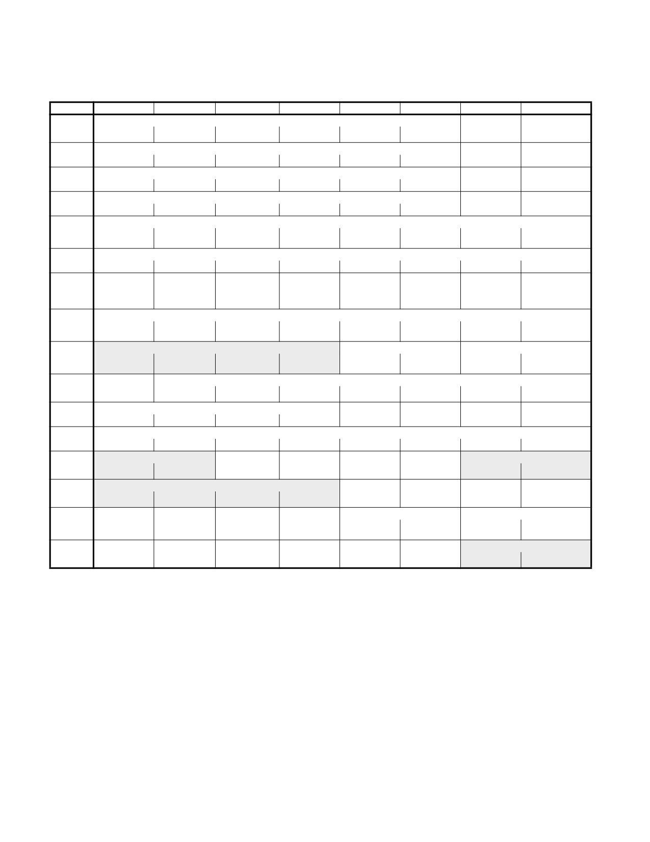
Table A-2. One-byte Opcode Map: (00H — F7H) *
0
1
2
3
4
5
6
7
0
ADD
PUSH
POP
ESi64
ESi64
Eb, Gb
Ev, Gv
Gb, Eb
Gv, Ev
AL, Ib
rAX, Iz
1
ADC
PUSH
POP
SSi64
SSi64
Eb, Gb
Ev, Gv
Gb, Eb
Gv, Ev
AL, Ib
rAX, Iz
2
AND
SEG=ES
DAAi64
(Prefix)
Eb, Gb
Ev, Gv
Gb, Eb
Gv, Ev
AL, Ib
rAX, Iz
3
XOR
SEG=SS
AAAi64
(Prefix)
Eb, Gb
Ev, Gv
Gb, Eb
Gv, Ev
AL, Ib
rAX, Iz
4
INCi64 general register / REXo64 Prefixes
eAX
eCX
eDX
eBX
eSP
eBP
eSI
eDI
REX
REX.B
REX.X
REX.XB
REX.R
REX.RB
REX.RX
REX.RXB
5
PUSHd64 general register
rAX/r8
rCX/r9
rDX/r10
rBX/r11
rSP/r12
rBP/r13
rSI/r14
rDI/r15
6
PUSHAi64/
POPAi64/
BOUNDi64
ARPLi64
SEG=FS
SEG=GS
Operand
Address
PUSHADi64
POPADi64
Gv, Ma
Ew, Gw
(Prefix)
(Prefix)
Size
Size
MOVSXDo64
(Prefix)
(Prefix)
Gv, Ev
7
Jccf64, Jb - Short-displacement jump on condition
O
NO
B/NAE/C
NB/AE/NC
Z/E
NZ/NE
BE/NA
NBE/A
8
Immediate Grp 11A
TEST
XCHG
Eb, Ib
Ev, Iz
Eb, Ibi64
Ev, Ib
Eb, Gb
Ev, Gv
Eb, Gb
Ev, Gv
9
NOP
XCHG word, double-word or quad-word register with rAX
PAUSE(F3)
rCX/r9
rDX/r10
rBX/r11
rSP/r12
rBP/r13
rSI/r14
rDI/r15
XCHG r8, rAX
A
MOV
MOVS/B
MOVS/W/D/Q
CMPS/B
CMPS/W/D
Yb, Xb
Yv, Xv
Xb, Yb
Xv, Yv
AL, Ob
rAX, Ov
Ob, AL
Ov, rAX
B
MOV immediate byte into byte register
AL/R8B, Ib
CL/R9B, Ib
DL/R10B, Ib
BL/R11B, Ib
AH/R12B, Ib
CH/R13B, Ib
DH/R14B, Ib
BH/R15B, Ib
1A
C
Shift Grp 2
near RETf64
near RETf64
LESi64
LDSi64
Grp 111A - MOV
Iw
Gz, Mp
Gz, Mp
Eb, Ib
Ev, Ib
Eb, Ib
Ev, Iz
VEX+2byte
VEX+1byte
D
Shift Grp 21A
AAMi64
AADi64
XLAT/
Ib
Ib
XLATB
Eb, 1
Ev, 1
Eb, CL
Ev, CL
E
LOOPNEf64/
LOOPEf64/
LOOPf64
JrCXZf64/
IN
OUT
LOOPNZf64
LOOPZf64
Jb
Jb
AL, Ib
eAX, Ib
Ib, AL
Ib, eAX
Jb
Jb
F
LOCK
INT1
REPNE
REP/REPE
HLT
CMC
Unary Grp 31A
(Prefix)
XACQUIRE
XRELEASE
Eb
Ev
(Prefix)
(Prefix)
Vol. 2D A-7

OPCODE MAP
Table A-2. One-byte Opcode Map: (08H — FFH) *
8
9
A
B
C
D
E
F
0
OR
PUSH
2-byte
CSi64
escape
Eb, Gb
Ev, Gv
Gb, Eb
Gv, Ev
AL, Ib
rAX, Iz
(Table A-3)
1
SBB
PUSH
POP
DSi64
DSi64
Eb, Gb
Ev, Gv
Gb, Eb
Gv, Ev
AL, Ib
rAX, Iz
2
SUB
SEG=CS
DASi64
(Prefix)
Eb, Gb
Ev, Gv
Gb, Eb
Gv, Ev
AL, Ib
rAX, Iz
3
CMP
SEG=DS
AASi64
(Prefix)
Eb, Gb
Ev, Gv
Gb, Eb
Gv, Ev
AL, Ib
rAX, Iz
4
DECi64 general register / REXo64 Prefixes
eAX
eCX
eDX
eBX
eSP
eBP
eSI
eDI
REX.W
REX.WB
REX.WX
REX.WXB
REX.WR
REX.WRB
REX.WRX
REX.WRXB
5
POPd64 into general register
rAX/r8
rCX/r9
rDX/r10
rBX/r11
rSP/r12
rBP/r13
rSI/r14
rDI/r15
6
PUSHd64
IMUL
PUSHd64
IMUL
INS/
INS/
OUTS/
OUTS/
Iz
Gv, Ev, Iz
Ib
Gv, Ev, Ib
INSB
INSW/
OUTSB
OUTSW/
Yb, DX
INSD
DX, Xb
OUTSD
Yz, DX
DX, Xz
7
Jccf64, Jb- Short displacement jump on condition
S
NS
P/PE
NP/PO
L/NGE
NL/GE
LE/NG
NLE/G
8
MOV
MOV
LEA
MOV
Grp 1A1A POPd64
Ev, Sw
Gv, M
Sw, Ew
Ev
Eb, Gb
Ev, Gv
Gb, Eb
Gv, Ev
9
CBW/
CWD/
far CALLi64
FWAIT/
PUSHF/D/Q d64/
POPF/D/Q d64/
SAHF
LAHF
CWDE/
CDQ/
Ap
WAIT
Fv
Fv
CDQE
CQO
A
TEST
STOS/B
STOS/W/D/Q
LODS/B
LODS/W/D/Q
SCAS/B
SCAS/W/D/Q
Yb, AL
Yv, rAX
AL, Xb
rAX, Xv
AL, Yb
rAX, Yv
AL, Ib
rAX, Iz
B
MOV immediate word or double into word, double, or quad register
rAX/r8, Iv
rCX/r9, Iv
rDX/r10, Iv
rBX/r11, Iv
rSP/r12, Iv
rBP/r13, Iv
rSI/r14, Iv
rDI/r15 , Iv
C
ENTER
LEAVEd64
far RET
far RET
INT3
INT
INTOi64
IRET/D/Q
Iw, Ib
Iw
Ib
D
ESC (Escape to coprocessor instruction set)
E
near CALLf64
JMP
IN
OUT
Jz
nearf64
fari64
shortf64
AL, DX
eAX, DX
DX, AL
DX, eAX
Jz
Ap
Jb
F
CLC
STC
CLI
STI
CLD
STD
INC/DEC
INC/DEC
Grp 41A
Grp 51A
NOTES:
* All blanks in all opcode maps are reserved and must not be used. Do not depend on the operation of undefined or reserved locations.
A-8
Vol. 2D

OPCODE MAP
Table A-3. Two-byte Opcode Map: 00H — 77H (First Byte is 0FH) *
pfx
0
1
2
3
4
5
6
7
Grp 61A
Grp 71A
LAR
LSL
SYSCALLo64
CLTS
SYSRETo64
0
Gv, Ew
Gv, Ew
vmovups
vmovups
vmovlps
vmovlps
vunpcklps
vunpckhps
vmovhpsv1
vmovhpsv1
Vps, Wps
Wps, Vps
Vq, Hq, Mq
Mq, Vq
Vx, Hx, Wx
Vx, Hx, Wx
Vdq, Hq, Mq
Mq, Vq
vmovhlps
vmovlhps
Vq, Hq, Uq
Vdq, Hq, Uq
1
vmovupd
vmovupd
vmovlpd
vmovlpd
vunpcklpd
vunpckhpd
vmovhpdv1
vmovhpdv1
66
Vpd, Wpd
Wpd,Vpd
Vq, Hq, Mq
Mq, Vq
Vx,Hx,Wx
Vx,Hx,Wx
Vdq, Hq, Mq
Mq, Vq
vmovss
vmovss
vmovsldup
vmovshdup
F3
Vx, Hx, Wss
Wss, Hx, Vss
Vx, Wx
Vx, Wx
vmovsd
vmovsd
vmovddup
F2
Vx, Hx, Wsd
Wsd, Hx, Vsd
Vx, Wx
MOV
MOV
MOV
MOV
Rd, Cd
Rd, Dd
Cd, Rd
Dd, Rd
2
WRMSR
RDTSC
RDMSR
RDPMC
SYSENTER
SYSEXIT
GETSEC
3
CMOVcc, (Gv, Ev) - Conditional Move
4
O
NO
B/C/NAE
AE/NB/NC
E/Z
NE/NZ
BE/NA
A/NBE
vmovmskps
vsqrtps
vrsqrtps
vrcpps
vandps
vandnps
vorps
vxorps
Gy, Ups
Vps, Wps
Vps, Wps
Vps, Wps
Vps, Hps, Wps
Vps, Hps, Wps
Vps, Hps, Wps
Vps, Hps, Wps
vmovmskpd
vsqrtpd
vandpd
vandnpd
vorpd
vxorpd
66
5
Gy,Upd
Vpd, Wpd
Vpd, Hpd, Wpd
Vpd, Hpd, Wpd
Vpd, Hpd, Wpd
Vpd, Hpd, Wpd
vsqrtss
vrsqrtss
vrcpss
F3
Vss, Hss, Wss
Vss, Hss, Wss
Vss, Hss, Wss
vsqrtsd
F2
Vsd, Hsd, Wsd
punpcklbw
punpcklwd
punpckldq
packsswb
pcmpgtb
pcmpgtw
pcmpgtd
packuswb
Pq, Qd
Pq, Qd
Pq, Qd
Pq, Qq
Pq, Qq
Pq, Qq
Pq, Qq
Pq, Qq
6
vpunpcklbw
vpunpcklwd
vpunpckldq
vpacksswb
vpcmpgtb
vpcmpgtw
vpcmpgtd
vpackuswb
66
Vx, Hx, Wx
Vx, Hx, Wx
Vx, Hx, Wx
Vx, Hx, Wx
Vx, Hx, Wx
Vx, Hx, Wx
Vx, Hx, Wx
Vx, Hx, Wx
F3
pshufw
(Grp 121A)
(Grp 131A)
(Grp 141A)
pcmpeqb
pcmpeqw
pcmpeqd
emms
Pq, Qq, Ib
Pq, Qq
Pq, Qq
Pq, Qq
vzeroupperv
vzeroallv
vpshufd
vpcmpeqb
vpcmpeqw
vpcmpeqd
7
66
Vx, Wx, Ib
Vx, Hx, Wx
Vx, Hx, Wx
Vx, Hx, Wx
vpshufhw
F3
Vx, Wx, Ib
vpshuflw
F2
Vx, Wx, Ib
Vol. 2D A-9

OPCODE MAP
Table A-3. Two-byte Opcode Map: 08H — 7FH (First Byte is 0FH) *
pfx
8
9
A
B
C
D
E
F
INVD
WBINVD
2-byte Illegal
prefetchw(/1)
0
Opcodes
Ev
UD21B
Prefetch1C
Reserved-NOP
bndldx
bndstx
Reserved-NOP
NOP /0 Ev
(Grp 161A)
66
bndmov
bndmov
1
F3
bndcl
bndmk
bndcu
bndcn
F2
vmovaps
vmovaps
cvtpi2ps
vmovntps
cvttps2pi
cvtps2pi
vucomiss
vcomiss
Vps, Wps
Wps, Vps
Vps, Qpi
Mps, Vps
Ppi, Wps
Ppi, Wps
Vss, Wss
Vss, Wss
vmovapd
vmovapd
cvtpi2pd
vmovntpd
cvttpd2pi
cvtpd2pi
vucomisd
vcomisd
66
Vpd, Wpd
Wpd,Vpd
Vpd, Qpi
Mpd, Vpd
Ppi, Wpd
Qpi, Wpd
Vsd, Wsd
Vsd, Wsd
2
vcvtsi2ss
vcvttss2si
vcvtss2si
F3
Vss, Hss, Ey
Gy, Wss
Gy, Wss
vcvtsi2sd
vcvttsd2si
vcvtsd2si
F2
Vsd, Hsd, Ey
Gy, Wsd
Gy, Wsd
3-byte escape
3-byte escape
3
(Table A-4)
(Table A-5)
CMOVcc(Gv, Ev) - Conditional Move
S
NS
P/PE
NP/PO
L/NGE
NL/GE
LE/NG
NLE/G
4
vaddps
vmulps
vcvtps2pd
vcvtdq2ps
vsubps
vminps
vdivps
vmaxps
Vps, Hps, Wps
Vps, Hps, Wps
Vpd, Wps
Vps, Wdq
Vps, Hps, Wps
Vps, Hps, Wps
Vps, Hps, Wps
Vps, Hps, Wps
vaddpd
vmulpd
vcvtpd2ps
vcvtps2dq
vsubpd
vminpd
vdivpd
vmaxpd
66
Vpd, Hpd, Wpd
Vpd, Hpd, Wpd
Vps, Wpd
Vdq, Wps
Vpd, Hpd, Wpd
Vpd, Hpd, Wpd
Vpd, Hpd, Wpd
Vpd, Hpd, Wpd
5
vaddss
vmulss
vcvtss2sd
vcvttps2dq
vsubss
vminss
vdivss
vmaxss
F3
Vss, Hss, Wss
Vss, Hss, Wss
Vsd, Hx, Wss
Vdq, Wps
Vss, Hss, Wss
Vss, Hss, Wss
Vss, Hss, Wss
Vss, Hss, Wss
vaddsd
vmulsd
vcvtsd2ss
vsubsd
vminsd
vdivsd
vmaxsd
F2
Vsd, Hsd, Wsd
Vsd, Hsd, Wsd
Vss, Hx, Wsd
Vsd, Hsd, Wsd
Vsd, Hsd, Wsd
Vsd, Hsd, Wsd
Vsd, Hsd, Wsd
punpckhbw
punpckhwd
punpckhdq
packssdw
movd/q
movq
Pq, Qd
Pq, Qd
Pq, Qd
Pq, Qd
Pd, Ey
Pq, Qq
vpunpckhbw
vpunpckhwd
vpunpckhdq
vpackssdw
vpunpcklqdq
vpunpckhqdq
vmovd/q
vmovdqa
6
66
Vx, Hx, Wx
Vx, Hx, Wx
Vx, Hx, Wx
Vx, Hx, Wx
Vx, Hx, Wx
Vx, Hx, Wx
Vy, Ey
Vx, Wx
vmovdqu
F3
Vx, Wx
VMREAD
VMWRITE
movd/q
movq
Ey, Gy
Gy, Ey
Ey, Pd
Qq, Pq
vhaddpd
vhsubpd
vmovd/q
vmovdqa
66
Vpd, Hpd, Wpd
Vpd, Hpd, Wpd
Ey, Vy
Wx,Vx
7
vmovq
vmovdqu
F3
Vq, Wq
Wx,Vx
vhaddps
vhsubps
Vps, Hps, Wps
Vps, Hps, Wps
F2
A-10
Vol. 2D

OPCODE MAP
Table A-3. Two-byte Opcode Map: 80H — F7H (First Byte is 0FH) *
pfx
0
1
2
3
4
5
6
7
Jccf64, Jz - Long-displacement jump on condition
8
O
NO
B/CNAE
AE/NB/NC
E/Z
NE/NZ
BE/NA
A/NBE
SETcc, Eb - Byte Set on condition
9
O
NO
B/C/NAE
AE/NB/NC
E/Z
NE/NZ
BE/NA
A/NBE
PUSHd64
POPd64
CPUID
BT
SHLD
SHLD
A
FS
FS
Ev, Gv
Ev, Gv, Ib
Ev, Gv, CL
CMPXCHG
LSS
BTR
LFS
LGS
MOVZX
B
Gv, Mp
Ev, Gv
Gv, Mp
Gv, Mp
Eb, Gb
Ev, Gv
Gv, Eb
Gv, Ew
XADD
XADD
vcmpps
movnti
pinsrw
pextrw
vshufps
Grp 91A
Eb, Gb
Ev, Gv
Vps,Hps,Wps,Ib
My, Gy
Pq,Ry/Mw,Ib
Gd, Nq, Ib
Vps,Hps,Wps,Ib
vcmppd
vpinsrw
vpextrw
vshufpd
66
Vpd,Hpd,Wpd,Ib
Vdq,Hdq,Ry/Mw,Ib
Gd, Udq, Ib
Vpd,Hpd,Wpd,Ib
C
vcmpss
F3
Vss,Hss,Wss,Ib
vcmpsd
F2
Vsd,Hsd,Wsd,Ib
psrlw
psrld
psrlq
paddq
pmullw
pmovmskb
Pq, Qq
Pq, Qq
Pq, Qq
Pq, Qq
Pq, Qq
Gd, Nq
vaddsubpd
vpsrlw
vpsrld
vpsrlq
vpaddq
vpmullw
vmovq
vpmovmskb
66
Vpd, Hpd, Wpd
Vx, Hx, Wx
Vx, Hx, Wx
Vx, Hx, Wx
Vx, Hx, Wx
Vx, Hx, Wx
Wq, Vq
Gd, Ux
D
movq2dq
F3
Vdq, Nq
vaddsubps
movdq2q
F2
Vps, Hps, Wps
Pq, Uq
pavgb
psraw
psrad
pavgw
pmulhuw
pmulhw
movntq
Pq, Qq
Pq, Qq
Pq, Qq
Pq, Qq
Pq, Qq
Pq, Qq
Mq, Pq
vpavgb
vpsraw
vpsrad
vpavgw
vpmulhuw
vpmulhw
vcvttpd2dq
vmovntdq
66
Vx, Hx, Wx
Vx, Hx, Wx
Vx, Hx, Wx
Vx, Hx, Wx
Vx, Hx, Wx
Vx, Hx, Wx
Vx, Wpd
Mx, Vx
E
vcvtdq2pd
F3
Vx, Wpd
vcvtpd2dq
F2
Vx, Wpd
psllw
pslld
psllq
pmuludq
pmaddwd
psadbw
maskmovq
Pq, Qq
Pq, Qq
Pq, Qq
Pq, Qq
Pq, Qq
Pq, Qq
Pq, Nq
vpsllw
vpslld
vpsllq
vpmuludq
vpmaddwd
vpsadbw
vmaskmovdqu
F
66
Vx, Hx, Wx
Vx, Hx, Wx
Vx, Hx, Wx
Vx, Hx, Wx
Vx, Hx, Wx
Vx, Hx, Wx
Vdq, Udq
vlddqu
F2
Vx, Mx
Vol. 2D A-11

OPCODE MAP
Table A-3. Two-byte Opcode Map: 88H — FFH (First Byte is 0FH) *
pfx
8
9
A
B
C
D
E
F
Jccf64, Jz - Long-displacement jump on condition
8
S
NS
P/PE
NP/PO
L/NGE
NL/GE
LE/NG
NLE/G
SETcc, Eb - Byte Set on condition
9
S
NS
P/PE
NP/PO
L/NGE
NL/GE
LE/NG
NLE/G
d64
PUSH
POPd64
RSM
BTS
SHRD
SHRD
(Grp 151A)1C
IMUL
A
GS
GS
Ev, Gv
Ev, Gv, Ib
Ev, Gv, CL
Gv, Ev
JMPE
Grp 101A
Grp 81A
BTC
BSF
BSR
MOVSX
(reserved for
Invalid Opcode1B
Ev, Ib
Ev, Gv
Gv, Ev
Gv, Ev
Gv, Eb
Gv, Ew
B
emulator on IPF)
POPCNT
TZCNT
LZCNT
F3
Gv, Ev
Gv, Ev
Gv, Ev
BSWAP
RAX/EAX/
RCX/ECX/
RDX/EDX/
RBX/EBX/
RSP/ESP/
RBP/EBP/
RSI/ESI/
RDI/EDI/
R8/R8D
R9/R9D
R10/R10D
R11/R11D
R12/R12D
R13/R13D
R14/R14D
R15/R15D
C
psubusb
psubusw
pminub
pand
paddusb
paddusw
pmaxub
pandn
Pq, Qq
Pq, Qq
Pq, Qq
Pq, Qq
Pq, Qq
Pq, Qq
Pq, Qq
Pq, Qq
vpsubusb
vpsubusw
vpminub
vpand
vpaddusb
vpaddusw
vpmaxub
vpandn
66
Vx, Hx, Wx
Vx, Hx, Wx
Vx, Hx, Wx
Vx, Hx, Wx
Vx, Hx, Wx
Vx, Hx, Wx
Vx, Hx, Wx
Vx, Hx, Wx
D
F3
F2
psubsb
psubsw
pminsw
por
paddsb
paddsw
pmaxsw
pxor
Pq, Qq
Pq, Qq
Pq, Qq
Pq, Qq
Pq, Qq
Pq, Qq
Pq, Qq
Pq, Qq
vpsubsb
vpsubsw
vpminsw
vpor
vpaddsb
vpaddsw
vpmaxsw
vpxor
66
Vx, Hx, Wx
Vx, Hx, Wx
Vx, Hx, Wx
Vx, Hx, Wx
Vx, Hx, Wx
Vx, Hx, Wx
Vx, Hx, Wx
Vx, Hx, Wx
E
F3
F2
psubb
psubw
psubd
psubq
paddb
paddw
paddd
Pq, Qq
Pq, Qq
Pq, Qq
Pq, Qq
Pq, Qq
Pq, Qq
Pq, Qq
UD0
vpsubb
vpsubw
vpsubd
vpsubq
vpaddb
vpaddw
vpaddd
F
66
Vx, Hx, Wx
Vx, Hx, Wx
Vx, Hx, Wx
Vx, Hx, Wx
Vx, Hx, Wx
Vx, Hx, Wx
Vx, Hx, Wx
F2
NOTES:
* All blanks in all opcode maps are reserved and must not be used. Do not depend on the operation of undefined or reserved locations.
A-12
Vol. 2D

OPCODE MAP
Table A-4. Three-byte Opcode Map: 00H — F7H (First Two Bytes are 0F 38H) *
pfx
0
1
2
3
4
5
6
7
pshufb
phaddw
phaddd
phaddsw
pmaddubsw
phsubw
phsubd
phsubsw
Pq, Qq
Pq, Qq
Pq, Qq
Pq, Qq
Pq, Qq
Pq, Qq
Pq, Qq
Pq, Qq
0
vpshufb
vphaddw
vphaddd
vphaddsw
vpmaddubsw
vphsubw
vphsubd
vphsubsw
66
Vx, Hx, Wx
Vx, Hx, Wx
Vx, Hx, Wx
Vx, Hx, Wx
Vx, Hx, Wx
Vx, Hx, Wx
Vx, Hx, Wx
Vx, Hx, Wx
pblendvb
vcvtph2psv
blendvps
blendvpd
vpermpsv
vptest
Vdq, Wdq
Vx, Wx, Ib
Vdq, Wdq
Vdq, Wdq
Vqq, Hqq, Wqq
Vx, Wx
1
66
vpmovsxbw
vpmovsxbd
vpmovsxbq
vpmovsxwd
vpmovsxwq
vpmovsxdq
2
66
Vx, Ux/Mq
Vx, Ux/Md
Vx, Ux/Mw
Vx, Ux/Mq
Vx, Ux/Md
Vx, Ux/Mq
vpmovzxbw
vpmovzxbd
vpmovzxbq
vpmovzxwd
vpmovzxwq
vpmovzxdq
vpermd
v
vpcmpgtq
3
66
Vx, Ux/Mq
Vx, Ux/Md
Vx, Ux/Mw
Vx, Ux/Mq
Vx, Ux/Md
Vx, Ux/Mq
Vqq, Hqq, Wqq
Vx, Hx, Wx
v
vpmulld
vphminposuw
vpsrlvd/q
vpsravdv
vpsllvd/qv
4
66
Vx, Hx, Wx
Vdq, Wdq
Vx, Hx, Wx
Vx, Hx, Wx
Vx, Hx, Wx
5
6
7
INVEPT
INVVPID
INVPCID
Gy, Mdq
Gy, Mdq
Gy, Mdq
8
66
vgatherdd/qv
vgatherqd/qv
vgatherdps/dv
vgatherqps/dv
vfmaddsub132ps/dv
vfmsubadd132ps/dv
9
66
Vx,Hx,Wx
Vx,Hx,Wx
Vx,Hx,Wx
Vx,Hx,Wx
Vx,Hx,Wx
Vx,Hx,Wx
vfmaddsub213ps/dv
vfmsubadd213ps/dv
A
66
Vx,Hx,Wx
Vx,Hx,Wx
vfmaddsub231ps/dv
vfmsubadd231ps/dv
B
66
Vx,Hx,Wx
Vx,Hx,Wx
C
D
E
MOVBE
MOVBE
ANDNv
BZHIv
BEXTRv
Gy, My
My, Gy
Gy, By, Ey
Gy, Ey, By
Gy, Ey, By
v
MOVBE
MOVBE
ADCX
SHLX
66
Gw, Mw
Mw, Gw
Gy, Ey
Gy, Ey, By
PEXT
v
ADOX
SARXv
F
F3
Grp 171A
Gy, By, Ey
Gy, Ey
Gy, Ey, By
v
CRC32
CRC32
PDEP
MULXv
SHRXv
F2
Gd, Eb
Gd, Ey
Gy, By, Ey
By,Gy,rDX,Ey
Gy, Ey, By
66 &
CRC32
CRC32
F2
Gd, Eb
Gd, Ew
Vol. 2D A-13

OPCODE MAP
Table A-4. Three-byte Opcode Map: 08H — FFH (First Two Bytes are 0F 38H) *
pfx
8
9
A
B
C
D
E
F
psignb
psignw
psignd
pmulhrsw
Pq, Qq
Pq, Qq
Pq, Qq
Pq, Qq
0
vpsignb
vpsignw
vpsignd
vpmulhrsw
vpermilpsv
vpermilpdv
vtestpsv
vtestpdv
66
Vx, Hx, Wx
Vx, Hx, Wx
Vx, Hx, Wx
Vx, Hx, Wx
Vx,Hx,Wx
Vx,Hx,Wx
Vx, Wx
Vx, Wx
pabsb
pabsw
pabsd
1
Pq, Qq
Pq, Qq
Pq, Qq
vbroadcastssv
vbroadcastsdv Vqq,
vbroadcastf128v Vqq,
vpabsb
vpabsw
vpabsd
66
Vx, Wd
Wq
Mdq
Vx, Wx
Vx, Wx
Vx, Wx
vpmuldq
vpcmpeqq
vmovntdqa
vpackusdw
vmaskmovpsv
vmaskmovpdv
vmaskmovpsv
vmaskmovpdv
2
66
Vx, Hx, Wx
Vx, Hx, Wx
Vx, Mx
Vx, Hx, Wx
Vx,Hx,Mx
Vx,Hx,Mx
Mx,Hx,Vx
Mx,Hx,Vx
vpminsb
vpminsd
vpminuw
vpminud
vpmaxsb
vpmaxsd
vpmaxuw
vpmaxud
3
66
Vx, Hx, Wx
Vx, Hx, Wx
Vx, Hx, Wx
Vx, Hx, Wx
Vx, Hx, Wx
Vx, Hx, Wx
Vx, Hx, Wx
Vx, Hx, Wx
4
vpbroadcastdv
vpbroadcastqv
vbroadcasti128v
5
66
Vx, Wx
Vx, Wx
Vqq, Mdq
6
vpbroadcastbv
vpbroadcastwv
7
66
Vx, Wx
Vx, Wx
vpmaskmovd/qv
vpmaskmovd/qv
8
66
Vx,Hx,Mx
Mx,Vx,Hx
vfmadd132ps/dv
vfmadd132ss/dv
vfmsub132ps/dv
vfmsub132ss/dv
vfnmadd132ps/dv
vfnmadd132ss/dv
vfnmsub132ps/dv
vfnmsub132ss/dv
9
66
Vx, Hx, Wx
Vx, Hx, Wx
Vx, Hx, Wx
Vx, Hx, Wx
Vx, Hx, Wx
Vx, Hx, Wx
Vx, Hx, Wx
Vx, Hx, Wx
vfmadd213ps/dv
vfmadd213ss/dv
vfmsub213ps/dv
vfmsub213ss/dv
vfnmadd213ps/dv
vfnmadd213ss/dv
vfnmsub213ps/dv
vfnmsub213ss/dv
A
66
Vx, Hx, Wx
Vx, Hx, Wx
Vx, Hx, Wx
Vx, Hx, Wx
Vx, Hx, Wx
Vx, Hx, Wx
Vx, Hx, Wx
Vx, Hx, Wx
vfmadd231ps/dv
vfmadd231ss/dv
vfmsub231ps/dv
vfmsub231ss/dv
vfnmadd231ps/dv
vfnmadd231ss/dv
vfnmsub231ps/dv
vfnmsub231ss/dv
B
66
Vx, Hx, Wx
Vx, Hx, Wx
Vx, Hx, Wx
Vx, Hx, Wx
Vx, Hx, Wx
Vx, Hx, Wx
Vx, Hx, Wx
Vx, Hx, Wx
sha1nexte
sha1msg1
sha1msg2
sha256rnds2
sha256msg1
sha256msg2
C
Vdq,Wdq
Vdq,Wdq
Vdq,Wdq
Vdq,Wdq
Vdq,Wdq
Vdq,Wdq
66
VAESIMC
VAESENC
VAESENCLAST
VAESDEC
VAESDECLAST
D
66
Vdq, Wdq
Vdq,Hdq,Wdq
Vdq,Hdq,Wdq
Vdq,Hdq,Wdq
Vdq,Hdq,Wdq
E
66
F
F3
F2
66 & F2
NOTES:
* All blanks in all opcode maps are reserved and must not be used. Do not depend on the operation of undefined or reserved locations.
A-14
Vol. 2D

OPCODE MAP
Table A-5. Three-byte Opcode Map: 00H — F7H (First two bytes are 0F 3AH) *
pfx
0
1
2
3
4
5
6
7
vpermqv
vpermpdv
vpblenddv
vpermilpsv
vpermilpdv
vperm2f128v
Vqq, Wqq, Ib
Vqq, Wqq, Ib
Vx,Hx,Wx,Ib
Vx, Wx, Ib
Vx, Wx, Ib
Vqq,Hqq,Wqq,Ib
0
66
vpextrb
vpextrw
vpextrd/q
vextractps
1
66
Rd/Mb, Vdq, Ib
Rd/Mw, Vdq, Ib
Ey, Vdq, Ib
Ed, Vdq, Ib
vpinsrb
vinsertps
vpinsrd/q
2
66
Vdq,Hdq,Ry/Mb,Ib
Vdq,Hdq,Udq/Md,Ib
Vdq,Hdq,Ey,Ib
3
v
vdpps
vdppd
vmpsadbw
vpclmulqdq
vperm2i128
4
66
Vx,Hx,Wx,Ib
Vdq,Hdq,Wdq,Ib
Vx,Hx,Wx,Ib
Vdq,Hdq,Wdq,Ib
Vqq,Hqq,Wqq,Ib
5
vpcmpestrm
vpcmpestri
vpcmpistrm
vpcmpistri
6
66
Vdq, Wdq, Ib
Vdq, Wdq, Ib
Vdq, Wdq, Ib
Vdq, Wdq, Ib
7
8
9
A
B
C
D
E
F
RORXv
F2
Gy, Ey, Ib
Vol. 2D A-15

OPCODE MAP
Table A-5. Three-byte Opcode Map: 08H — FFH (First Two Bytes are 0F 3AH) *
pfx
8
9
A
B
C
D
E
F
palignr
0
Pq, Qq, Ib
vroundps
vroundpd
vroundss
vroundsd
vblendps
vblendpd
vpblendw
vpalignr
66
Vx,Wx,Ib
Vx,Wx,Ib
Vss,Wss,Ib
Vsd,Wsd,Ib
Vx,Hx,Wx,Ib
Vx,Hx,Wx,Ib
Vx,Hx,Wx,Ib
Vx,Hx,Wx,Ib
vinsertf128v
vextractf128v
vcvtps2phv
1
66
Vqq,Hqq,Wqq,Ib
Wdq,Vqq,Ib
Wx, Vx, Ib
2
vinserti128v
vextracti128v
3
66
Vqq,Hqq,Wqq,Ib
Wdq,Vqq,Ib
v
vblendvps
vblendvpdv
vpblendvbv
4
66
Vx,Hx,Wx,Lx
Vx,Hx,Wx,Lx
Vx,Hx,Wx,Lx
5
6
7
8
9
A
B
sha1rnds4
C
Vdq,Wdq,Ib
VAESKEYGEN
D
66
Vdq, Wdq, Ib
E
F
NOTES:
* All blanks in all opcode maps are reserved and must not be used. Do not depend on the operation of undefined or reserved locations.
A-16
Vol. 2D

OPCODE MAP
A.4
OPCODE EXTENSIONS FOR ONE-BYTE AND TWO-BYTE OPCODES
Some 1-byte and 2-byte opcodes use bits 3-5 of the ModR/M byte (the nnn field in Figure A-1) as an extension of
the opcode.
mod
nnn
R/M
Figure A-1. ModR/M Byte nnn Field (Bits 5, 4, and 3)
Opcodes that have opcode extensions are indicated in Table A-6 and organized by group number. Group numbers
(from 1 to 16, second column) provide a table entry point. The encoding for the r/m field for each instruction can
be established using the third column of the table.
A.4.1
Opcode Look-up Examples Using Opcode Extensions
An Example is provided below.
Example A-4. Interpreting an ADD Instruction
An ADD instruction with a 1-byte opcode of 80H is a Group 1 instruction:
• Table A-6 indicates that the opcode extension field encoded in the ModR/M byte for this instruction is 000B.
• The r/m field can be encoded to access a register (11B) or a memory address using a specified addressing
mode (for example: mem = 00B, 01B, 10B).
Example A-5. Looking Up 0F01C3H
Look up opcode 0F01C3 for a VMRESUME instruction by using Table A-2, Table A-3, and Table A-6:
•
0F indicates that this instruction is in the 2-byte opcode map.
•
01 (row 0, column 1 in Table A-3) reveals that this opcode is in Group 7 of Table A-6.
• C3 is the ModR/M byte. The first two bits of C3 are 11B. This tells us to look at the second of the Group 7 rows
in Table A-6.
• The Op/Reg bits [5,4,3] are 000B. This tells us to look in the 000 column for Group 7.
• Finally, the R/M bits [2,1,0] are 011B. This identifies the opcode as the VMRESUME instruction.
A.4.2
Opcode Extension Tables
See Table A-6 below.
Vol. 2D A-17
OPCODE MAP
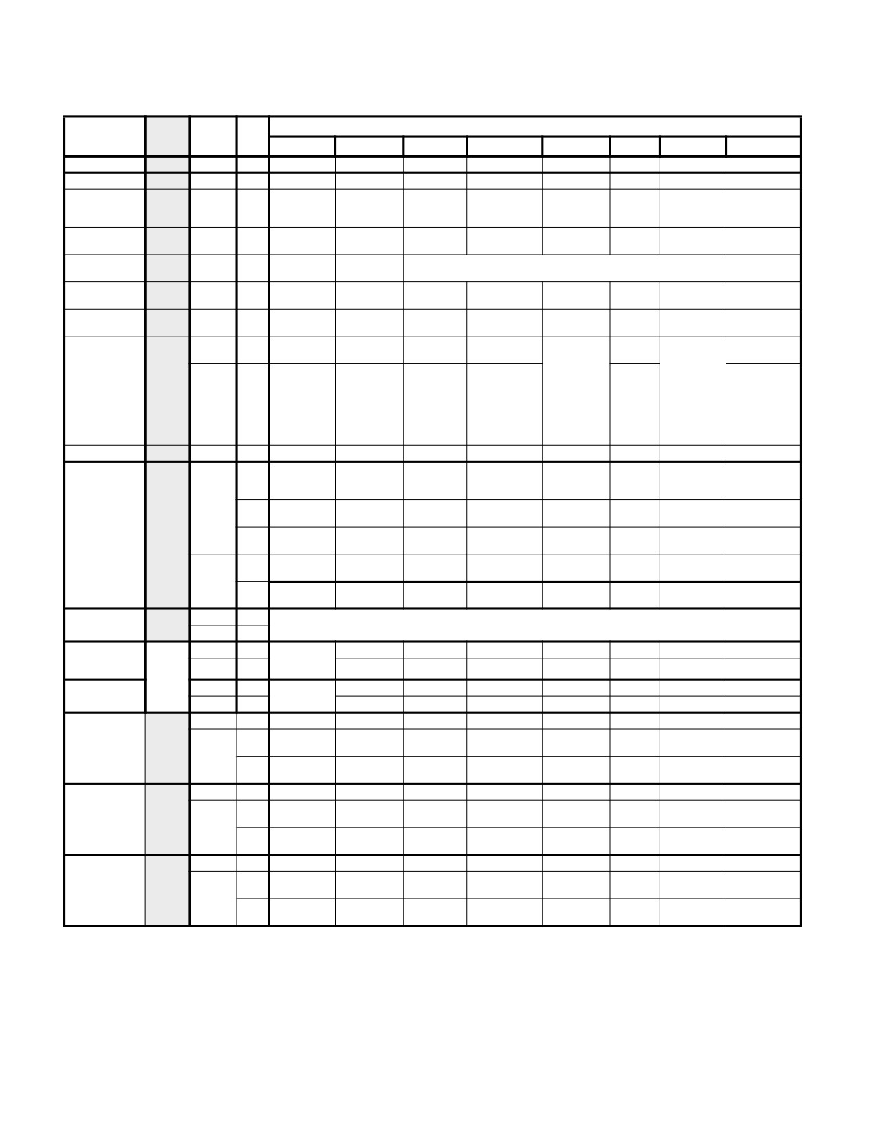
Table A-6. Opcode Extensions for One- and Two-byte Opcodes by Group Number *
Encoding of Bits 5,4,3 of the ModR/M Byte (bits 2,1,0 in parenthesis)
Opcode
Group
Mod 7,6
pfx
000
001
010
011
100
101
110
111
80-83
1
mem, 11B
ADD
OR
ADC
SBB
AND
SUB
XOR
CMP
8F
1A
mem, 11B
POP
C0,C1 reg, imm
mem, 11B
ROL
ROR
RCL
RCR
SHL/SAL
SHR
SAR
D0, D1 reg, 1
2
D2, D3 reg, CL
mem, 11B
TEST
NOT
NEG
MUL
IMUL
DIV
IDIV
F6, F7
3
Ib/Iz
AL/rAX
AL/rAX
AL/rAX
AL/rAX
mem, 11B
INC
DEC
FE
4
Eb
Eb
mem, 11B
INC
DEC
near CALL
f64
far CALL
near JMPf64
far JMP
PUSHd64
FF
5
Ev
Ev
Ev
Ep
Ev
Mp
Ev
mem, 11B
SLDT
STR
LLDT
LTR
VERR
VERW
0F 00
6
Rv/Mw
Rv/Mw
Ew
Ew
Ew
Ew
mem
SGDT
SIDT
LGDT
LIDT
SMSW
LMSW
INVLPG
Ms
Ms
Ms
Ms
Mw/Rv
Ew
Mb
11B
VMCALL (001)
MONITOR
XGETBV (000)
SWAPGS
VMLAUNCH
(000)
XSETBV (001)
o64(000)
0F 01
7
(010)
MWAIT (001)
RDTSCP (001)
VMFUNC
VMRESUME
CLAC (010)
(100)
(011) VMXOFF
STAC (011)
XEND (101)
(100)
ENCLS (111)
XTEST (110)
ENCLU(111)
0F BA
8
mem, 11B
BT
BTS
BTR
BTC
CMPXCH8B Mq
VMPTRLD
VMPTRST
CMPXCHG16B
Mq
Mq
Mdq
mem
66
VMCLEAR
Mq
0F C7
9
F3
VMXON
Mq
RDRAND
RDSEED
Rv
Rv
11B
F3
RDPID
Rd/q
mem
UD1
0F B9
10
11B
mem
MOV
C6
Eb, Ib
11B
XABORT (000) Ib
11
mem
MOV
C7
Ev, Iz
11B
XBEGIN (000) Jz
mem
psrlw
psraw
psllw
0F 71
12
Nq, Ib
Nq, Ib
Nq, Ib
11B
66
vpsrlw
vpsraw
vpsllw
Hx,Ux,Ib
Hx,Ux,Ib
Hx,Ux,Ib
mem
psrld
psrad
pslld
0F 72
13
Nq, Ib
Nq, Ib
Nq, Ib
11B
66
vpsrld
vpsrad
vpslld
Hx,Ux,Ib
Hx,Ux,Ib
Hx,Ux,Ib
mem
psrlq
psllq
0F 73
14
Nq, Ib
Nq, Ib
11B
66
vpsrlq
vpsrldq
vpsllq
vpslldq
Hx,Ux,Ib
Hx,Ux,Ib
Hx,Ux,Ib
Hx,Ux,Ib
A-18
Vol. 2D

OPCODE MAP
Table A-6. Opcode Extensions for One- and Two-byte Opcodes by Group Number * (Contd.)
Encoding of Bits 5,4,3 of the ModR/M Byte (bits 2,1,0 in parenthesis)
Opcode
Group
Mod 7,6
pfx
000
001
010
011
100
101
110
111
mem
fxsave
fxrstor
ldmxcsr
stmxcsr
XSAVE
XRSTOR
XSAVEOPT
clflush
lfence
mfence
sfence
0F AE
15
F3
RDFSBASE
RDGSBASE
WRFSBASE
WRGSBASE
11B
Ry
Ry
Ry
Ry
prefetch
prefetch
prefetch
prefetch
Reserved NOP
mem
NTA
T0
T1
T2
0F 18
16
11B
Reserved NOP
mem
BLSRv
BLSMSKv
BLSIv
VEX.0F38 F3
17
By, Ey
By, Ey
By, Ey
11B
NOTES:
* All blanks in all opcode maps are reserved and must not be used. Do not depend on the operation of undefined or reserved locations.
Vol. 2D A-19

OPCODE MAP
A.5
ESCAPE OPCODE INSTRUCTIONS
Opcode maps for coprocessor escape instruction opcodes (x87 floating-point instruction opcodes) are in Table A-7
through Table A-22. These maps are grouped by the first byte of the opcode, from D8-DF. Each of these opcodes
has a ModR/M byte. If the ModR/M byte is within the range of 00H-BFH, bits 3-5 of the ModR/M byte are used as
an opcode extension, similar to the technique used for 1-and 2-byte opcodes (see A.4). If the ModR/M byte is
outside the range of 00H through BFH, the entire ModR/M byte is used as an opcode extension.
A.5.1
Opcode Look-up Examples for Escape Instruction Opcodes
Examples are provided below.
Example A-6. Opcode with ModR/M Byte in the 00H through BFH Range
DD0504000000H can be interpreted as follows:
• The instruction encoded with this opcode can be located in Section . Since the ModR/M byte (05H) is within the
00H through BFH range, bits 3 through 5 (000) of this byte indicate the opcode for an FLD double-real
instruction (see Table A-9).
• The double-real value to be loaded is at 00000004H (the 32-bit displacement that follows and belongs to this
opcode).
Example A-7. Opcode with ModR/M Byte outside the 00H through BFH Range
D8C1H can be interpreted as follows:
• This example illustrates an opcode with a ModR/M byte outside the range of 00H through BFH. The instruction
can be located in Section A.4.
• In Table A-8, the ModR/M byte C1H indicates row C, column 1 (the FADD instruction using ST(0), ST(1) as
operands).
A.5.2
Escape Opcode Instruction Tables
Tables are listed below.
A.5.2.1
Escape Opcodes with D8 as First Byte
Table A-7 and A-8 contain maps for the escape instruction opcodes that begin with D8H. Table A-7 shows the map if the ModR/M
byte is in the range of 00H-BFH. Here, the value of bits 3-5 (the nnn field in Figure A-1) selects the instruction.
Table A-7. D8 Opcode Map When ModR/M Byte is Within 00H to BFH *
nnn Field of ModR/M Byte (refer to Figure A.4)
000B
001B
010B
011B
100B
101B
110B
111B
FADD
FMUL
FCOM
FCOMP
FSUB
FSUBR
FDIV
FDIVR
single-real
single-real
single-real
single-real
single-real
single-real
single-real
single-real
NOTES:
* All blanks in all opcode maps are reserved and must not be used. Do not depend on the operation of undefined or reserved locations.
A-20
Vol. 2D

OPCODE MAP
Table A-8 shows the map if the ModR/M byte is outside the range of 00H-BFH. Here, the first digit of the ModR/M byte selects the
table row and the second digit selects the column.
Table A-8. D8 Opcode Map When ModR/M Byte is Outside 00H to BFH *
0
1
2
3
4
5
6
7
C
FADD
ST(0),ST(0)
ST(0),ST(1)
ST(0),ST(2)
ST(0),ST(3)
ST(0),ST(4)
ST(0),ST(5)
ST(0),ST(6)
ST(0),ST(7)
D
FCOM
ST(0),ST(0)
ST(0),ST(1)
ST(0),T(2)
ST(0),ST(3)
ST(0),ST(4)
ST(0),ST(5)
ST(0),ST(6)
ST(0),ST(7)
E
FSUB
ST(0),ST(0)
ST(0),ST(1)
ST(0),ST(2)
ST(0),ST(3)
ST(0),ST(4)
ST(0),ST(5)
ST(0),ST(6)
ST(0),ST(7)
F
FDIV
ST(0),ST(0)
ST(0),ST(1)
ST(0),ST(2)
ST(0),ST(3)
ST(0),ST(4)
ST(0),ST(5)
ST(0),ST(6)
ST(0),ST(7)
8
9
A
B
C
D
E
F
C
FMUL
ST(0),ST(0)
ST(0),ST(1)
ST(0),ST(2)
ST(0),ST(3)
ST(0),ST(4)
ST(0),ST(5)
ST(0),ST(6)
ST(0),ST(7)
D
FCOMP
ST(0),ST(0)
ST(0),ST(1)
ST(0),T(2)
ST(0),ST(3)
ST(0),ST(4)
ST(0),ST(5)
ST(0),ST(6)
ST(0),ST(7)
E
FSUBR
ST(0),ST(0)
ST(0),ST(1)
ST(0),ST(2)
ST(0),ST(3)
ST(0),ST(4)
ST(0),ST(5)
ST(0),ST(6)
ST(0),ST(7)
F
FDIVR
ST(0),ST(0)
ST(0),ST(1)
ST(0),ST(2)
ST(0),ST(3)
ST(0),ST(4)
ST(0),ST(5)
ST(0),ST(6)
ST(0),ST(7)
NOTES:
* All blanks in all opcode maps are reserved and must not be used. Do not depend on the operation of undefined or reserved locations.
A.5.2.2
Escape Opcodes with D9 as First Byte
Table A-9 and A-10 contain maps for escape instruction opcodes that begin with D9H. Table A-9 shows the map if the ModR/M
byte is in the range of 00H-BFH. Here, the value of bits 3-5 (the nnn field in Figure A-1) selects the instruction.
Table A-9. D9 Opcode Map When ModR/M Byte is Within 00H to BFH *
nnn Field of ModR/M Byte
000B
001B
010B
011B
100B
101B
110B
111B
FLD
FST
FSTP
FLDENV
FLDCW
FSTENV
FSTCW
single-real
single-real
single-real
14/28 bytes
2 bytes
14/28 bytes
2 bytes
NOTES:
* All blanks in all opcode maps are reserved and must not be used. Do not depend on the operation of undefined or reserved locations.
Vol. 2D A-21

OPCODE MAP
Table A-10 shows the map if the ModR/M byte is outside the range of 00H-BFH. Here, the first digit of the ModR/M byte selects the
table row and the second digit selects the column.
Table A-10. D9 Opcode Map When ModR/M Byte is Outside 00H to BFH *
0
1
2
3
4
5
6
7
C
FLD
ST(0),ST(0)
ST(0),ST(1)
ST(0),ST(2)
ST(0),ST(3)
ST(0),ST(4)
ST(0),ST(5)
ST(0),ST(6)
ST(0),ST(7)
D
FNOP
E
FCHS
FABS
FTST
FXAM
F
F2XM1
FYL2X
FPTAN
FPATAN
FXTRACT
FPREM1
FDECSTP
FINCSTP
8
9
A
B
C
D
E
F
C
FXCH
ST(0),ST(0)
ST(0),ST(1)
ST(0),ST(2)
ST(0),ST(3)
ST(0),ST(4)
ST(0),ST(5)
ST(0),ST(6)
ST(0),ST(7)
D
E
FLD1
FLDL2T
FLDL2E
FLDPI
FLDLG2
FLDLN2
FLDZ
F
FPREM
FYL2XP1
FSQRT
FSINCOS
FRNDINT
FSCALE
FSIN
FCOS
NOTES:
* All blanks in all opcode maps are reserved and must not be used. Do not depend on the operation of undefined or reserved locations.
A.5.2.3
Escape Opcodes with DA as First Byte
Table A-11 and A-12 contain maps for escape instruction opcodes that begin with DAH. Table A-11 shows the map if the ModR/M
byte is in the range of 00H-BFH. Here, the value of bits 3-5 (the nnn field in Figure A-1) selects the instruction.
Table A-11. DA Opcode Map When ModR/M Byte is Within 00H to BFH *
nnn Field of ModR/M Byte
000B
001B
010B
011B
100B
101B
110B
111B
FIADD
FIMUL
FICOM
FICOMP
FISUB
FISUBR
FIDIV
FIDIVR
dword-integer
dword-integer
dword-integer
dword-integer
dword-integer
dword-integer
dword-integer
dword-integer
NOTES:
* All blanks in all opcode maps are reserved and must not be used. Do not depend on the operation of undefined or reserved locations.
A-22
Vol. 2D

OPCODE MAP
Table A-12 shows the map if the ModR/M byte is outside the range of 00H-BFH. Here, the first digit of the ModR/M byte selects
the table row and the second digit selects the column.
Table A-12. DA Opcode Map When ModR/M Byte is Outside 00H to BFH *
0
1
2
3
4
5
6
7
C
FCMOVB
ST(0),ST(0)
ST(0),ST(1)
ST(0),ST(2)
ST(0),ST(3)
ST(0),ST(4)
ST(0),ST(5)
ST(0),ST(6)
ST(0),ST(7)
D
FCMOVBE
ST(0),ST(0)
ST(0),ST(1)
ST(0),ST(2)
ST(0),ST(3)
ST(0),ST(4)
ST(0),ST(5)
ST(0),ST(6)
ST(0),ST(7)
E
F
8
9
A
B
C
D
E
F
C
FCMOVE
ST(0),ST(0)
ST(0),ST(1)
ST(0),ST(2)
ST(0),ST(3)
ST(0),ST(4)
ST(0),ST(5)
ST(0),ST(6)
ST(0),ST(7)
D
FCMOVU
ST(0),ST(0)
ST(0),ST(1)
ST(0),ST(2)
ST(0),ST(3)
ST(0),ST(4)
ST(0),ST(5)
ST(0),ST(6)
ST(0),ST(7)
E
FUCOMPP
F
NOTES:
* All blanks in all opcode maps are reserved and must not be used. Do not depend on the operation of undefined or reserved locations.
A.5.2.4
Escape Opcodes with DB as First Byte
Table A-13 and A-14 contain maps for escape instruction opcodes that begin with DBH. Table A-13 shows the map if the ModR/M
byte is in the range of 00H-BFH. Here, the value of bits 3-5 (the nnn field in Figure A-1) selects the instruction.
Table A-13. DB Opcode Map When ModR/M Byte is Within 00H to BFH *
nnn Field of ModR/M Byte
000B
001B
010B
011B
100B
101B
110B
111B
FILD
FISTTP
FIST
FISTP
FLD
FSTP
dword-integer
dword-integer
dword-integer
dword-integer
extended-real
extended-real
NOTES:
* All blanks in all opcode maps are reserved and must not be used. Do not depend on the operation of undefined or reserved locations.
Vol. 2D A-23

OPCODE MAP
Table A-14 shows the map if the ModR/M byte is outside the range of 00H-BFH. Here, the first digit of the ModR/M byte selects the
table row and the second digit selects the column.
Table A-14. DB Opcode Map When ModR/M Byte is Outside 00H to BFH *
0
1
2
3
4
5
6
7
C
FCMOVNB
ST(0),ST(0)
ST(0),ST(1)
ST(0),ST(2)
ST(0),ST(3)
ST(0),ST(4)
ST(0),ST(5)
ST(0),ST(6)
ST(0),ST(7)
D
FCMOVNBE
ST(0),ST(0)
ST(0),ST(1)
ST(0),ST(2)
ST(0),ST(3)
ST(0),ST(4)
ST(0),ST(5)
ST(0),ST(6)
ST(0),ST(7)
E
FCLEX
FINIT
F
FCOMI
ST(0),ST(0)
ST(0),ST(1)
ST(0),ST(2)
ST(0),ST(3)
ST(0),ST(4)
ST(0),ST(5)
ST(0),ST(6)
ST(0),ST(7)
8
9
A
B
C
D
E
F
C
FCMOVNE
ST(0),ST(0)
ST(0),ST(1)
ST(0),ST(2)
ST(0),ST(3)
ST(0),ST(4)
ST(0),ST(5)
ST(0),ST(6)
ST(0),ST(7)
D
FCMOVNU
ST(0),ST(0)
ST(0),ST(1)
ST(0),ST(2)
ST(0),ST(3)
ST(0),ST(4)
ST(0),ST(5)
ST(0),ST(6)
ST(0),ST(7)
E
FUCOMI
ST(0),ST(0)
ST(0),ST(1)
ST(0),ST(2)
ST(0),ST(3)
ST(0),ST(4)
ST(0),ST(5)
ST(0),ST(6)
ST(0),ST(7)
F
NOTES:
* All blanks in all opcode maps are reserved and must not be used. Do not depend on the operation of undefined or reserved locations.
A.5.2.5
Escape Opcodes with DC as First Byte
Table A-15 and A-16 contain maps for escape instruction opcodes that begin with DCH. Table A-15 shows the map if the ModR/M
byte is in the range of 00H-BFH. Here, the value of bits 3-5 (the nnn field in Figure A-1) selects the instruction.
Table A-15. DC Opcode Map When ModR/M Byte is Within 00H to BFH *
nnn Field of ModR/M Byte (refer to Figure A-1)
000B
001B
010B
011B
100B
101B
110B
111B
FADD
FMUL
FCOM
FCOMP
FSUB
FSUBR
FDIV
FDIVR
double-real
double-real
double-real
double-real
double-real
double-real
double-real
double-real
NOTES:
* All blanks in all opcode maps are reserved and must not be used. Do not depend on the operation of undefined or reserved locations.
A-24
Vol. 2D

OPCODE MAP
Table A-16 shows the map if the ModR/M byte is outside the range of 00H-BFH. In this case the first digit of the ModR/M byte
selects the table row and the second digit selects the column.
Table A-16. DC Opcode Map When ModR/M Byte is Outside 00H to BFH *
0
1
2
3
4
5
6
7
C
FADD
ST(0),ST(0)
ST(1),ST(0)
ST(2),ST(0)
ST(3),ST(0)
ST(4),ST(0)
ST(5),ST(0)
ST(6),ST(0)
ST(7),ST(0)
D
E
FSUBR
ST(0),ST(0)
ST(1),ST(0)
ST(2),ST(0)
ST(3),ST(0)
ST(4),ST(0)
ST(5),ST(0)
ST(6),ST(0)
ST(7),ST(0)
F
FDIVR
ST(0),ST(0)
ST(1),ST(0)
ST(2),ST(0)
ST(3),ST(0)
ST(4),ST(0)
ST(5),ST(0)
ST(6),ST(0)
ST(7),ST(0)
8
9
A
B
C
D
E
F
C
FMUL
ST(0),ST(0)
ST(1),ST(0)
ST(2),ST(0)
ST(3),ST(0)
ST(4),ST(0)
ST(5),ST(0)
ST(6),ST(0)
ST(7),ST(0)
D
E
FSUB
ST(0),ST(0)
ST(1),ST(0)
ST(2),ST(0)
ST(3),ST(0)
ST(4),ST(0)
ST(5),ST(0)
ST(6),ST(0)
ST(7),ST(0)
F
FDIV
ST(0),ST(0)
ST(1),ST(0)
ST(2),ST(0)
ST(3),ST(0)
ST(4),ST(0)
ST(5),ST(0)
ST(6),ST(0)
ST(7),ST(0)
NOTES:
* All blanks in all opcode maps are reserved and must not be used. Do not depend on the operation of undefined or reserved locations.
A.5.2.6
Escape Opcodes with DD as First Byte
Table A-17 and A-18 contain maps for escape instruction opcodes that begin with DDH. Table A-17 shows the map if the ModR/M
byte is in the range of 00H-BFH. Here, the value of bits 3-5 (the nnn field in Figure A-1) selects the instruction.
Table A-17. DD Opcode Map When ModR/M Byte is Within 00H to BFH *
nnn Field of ModR/M Byte
000B
001B
010B
011B
100B
101B
110B
111B
FLD
FISTTP
FST
FSTP
FRSTOR
FSAVE
FSTSW
double-real
integer64
double-real
double-real
98/108bytes
98/108bytes
2 bytes
NOTES:
* All blanks in all opcode maps are reserved and must not be used. Do not depend on the operation of undefined or reserved locations.
Vol. 2D A-25

OPCODE MAP
Table A-18 shows the map if the ModR/M byte is outside the range of 00H-BFH. The first digit of the ModR/M byte selects the table
row and the second digit selects the column.
Table A-18. DD Opcode Map When ModR/M Byte is Outside 00H to BFH *
0
1
2
3
4
5
6
7
C
FFREE
ST(0)
ST(1)
ST(2)
ST(3)
ST(4)
ST(5)
ST(6)
ST(7)
D
FST
ST(0)
ST(1)
ST(2)
ST(3)
ST(4)
ST(5)
ST(6)
ST(7)
E
FUCOM
ST(0),ST(0)
ST(1),ST(0)
ST(2),ST(0)
ST(3),ST(0)
ST(4),ST(0)
ST(5),ST(0)
ST(6),ST(0)
ST(7),ST(0)
F
8
9
A
B
C
D
E
F
C
D
FSTP
ST(0)
ST(1)
ST(2)
ST(3)
ST(4)
ST(5)
ST(6)
ST(7)
E
FUCOMP
ST(0)
ST(1)
ST(2)
ST(3)
ST(4)
ST(5)
ST(6)
ST(7)
F
NOTES:
* All blanks in all opcode maps are reserved and must not be used. Do not depend on the operation of undefined or reserved locations.
A.5.2.7
Escape Opcodes with DE as First Byte
Table A-19 and A-20 contain opcode maps for escape instruction opcodes that begin with DEH. Table A-19 shows the opcode map
if the ModR/M byte is in the range of 00H-BFH. In this case, the value of bits 3-5 (the nnn field in Figure A-1) selects the instruc-
tion.
Table A-19. DE Opcode Map When ModR/M Byte is Within 00H to BFH *
nnn Field of ModR/M Byte
000B
001B
010B
011B
100B
101B
110B
111B
FIADD
FIMUL
FICOM
FICOMP
FISUB
FISUBR
FIDIV
FIDIVR
word-integer
word-integer
word-integer
word-integer
word-integer
word-integer
word-integer
word-integer
NOTES:
* All blanks in all opcode maps are reserved and must not be used. Do not depend on the operation of undefined or reserved locations.
A-26
Vol. 2D

OPCODE MAP
Table A-20 shows the opcode map if the ModR/M byte is outside the range of 00H-BFH. The first digit of the ModR/M byte selects
the table row and the second digit selects the column.
Table A-20. DE Opcode Map When ModR/M Byte is Outside 00H to BFH *
0
1
2
3
4
5
6
7
C
FADDP
ST(0),ST(0)
ST(1),ST(0)
ST(2),ST(0)
ST(3),ST(0)
ST(4),ST(0)
ST(5),ST(0)
ST(6),ST(0)
ST(7),ST(0)
D
E
FSUBRP
ST(0),ST(0)
ST(1),ST(0)
ST(2),ST(0)
ST(3),ST(0)
ST(4),ST(0)
ST(5),ST(0)
ST(6),ST(0)
ST(7),ST(0)
F
FDIVRP
ST(0),ST(0)
ST(1),ST(0)
ST(2),ST(0)
ST(3),ST(0)
ST(4),ST(0)
ST(5),ST(0)
ST(6),ST(0)
ST(7),ST(0)
8
9
A
B
C
D
E
F
C
FMULP
ST(0),ST(0)
ST(1),ST(0)
ST(2),ST(0)
ST(3),ST(0)
ST(4),ST(0)
ST(5),ST(0)
ST(6),ST(0)
ST(7),ST(0)
D
FCOMPP
E
FSUBP
ST(0),ST(0)
ST(1),ST(0)
ST(2),ST(0)
ST(3),ST(0)
ST(4),ST(0)
ST(5),ST(0)
ST(6),ST(0)
ST(7),ST(0)
F
FDIVP
ST(0),ST(0)
ST(1),ST(0)
ST(2),ST(0).
ST(3),ST(0)
ST(4),ST(0)
ST(5),ST(0)
ST(6),ST(0)
ST(7),ST(0)
NOTES:
* All blanks in all opcode maps are reserved and must not be used. Do not depend on the operation of undefined or reserved locations.
A.5.2.8
Escape Opcodes with DF As First Byte
Table A-21 and A-22 contain the opcode maps for escape instruction opcodes that begin with DFH. Table A-21 shows the opcode
map if the ModR/M byte is in the range of 00H-BFH. Here, the value of bits 3-5 (the nnn field in Figure A-1) selects the instruction.
Table A-21. DF Opcode Map When ModR/M Byte is Within 00H to BFH *
nnn Field of ModR/M Byte
000B
001B
010B
011B
100B
101B
110B
111B
FILD
FISTTP
FIST
FISTP
FBLD
FILD
FBSTP
FISTP
word-integer
word-integer
word-integer
word-integer
packed-BCD
qword-integer
packed-BCD
qword-integer
NOTES:
* All blanks in all opcode maps are reserved and must not be used. Do not depend on the operation of undefined or reserved locations.
Vol. 2D A-27
OPCODE MAP
Table A-22 shows the opcode map if the ModR/M byte is outside the range of 00H-BFH. The first digit of the ModR/M byte selects
the table row and the second digit selects the column.
Table A-22. DF Opcode Map When ModR/M Byte is Outside 00H to BFH *
0
1
2
3
4
5
6
7
C
D
E
FSTSW
AX
F
FCOMIP
ST(0),ST(0)
ST(0),ST(1)
ST(0),ST(2)
ST(0),ST(3)
ST(0),ST(4)
ST(0),ST(5)
ST(0),ST(6)
ST(0),ST(7)
8
9
A
B
C
D
E
F
C
D
E
FUCOMIP
ST(0),ST(0)
ST(0),ST(1)
ST(0),ST(2)
ST(0),ST(3)
ST(0),ST(4)
ST(0),ST(5)
ST(0),ST(6)
ST(0),ST(7)
F
NOTES:
* All blanks in all opcode maps are reserved and must not be used. Do not depend on the operation of undefined or reserved locations.
A-28
Vol. 2D

OPCODE MAP
Vol. 2D A-29
OPCODE MAP
A-30
Vol. 2D

APPENDIX B
INSTRUCTION FORMATS AND ENCODINGS
This appendix provides machine instruction formats and encodings of IA-32 instructions. The first section describes
the IA-32 architecture’s machine instruction format. The remaining sections show the formats and encoding of
general-purpose, MMX, P6 family, SSE/SSE2/SSE3, x87 FPU instructions, and VMX instructions. Those instruction
formats also apply to Intel 64 architecture. Instruction formats used in 64-bit mode are provided as supersets of
the above.
B.1
MACHINE INSTRUCTION FORMAT
All Intel Architecture instructions are encoded using subsets of the general machine instruction format shown in
Figure B-1. Each instruction consists of:
•
an opcode
•
a register and/or address mode specifier consisting of the ModR/M byte and sometimes the scale-index-base
(SIB) byte (if required)
•
a displacement and an immediate data field (if required)
7 6 5 4 3 2 1 0
7 6 5 4 3 2 1 0
7 6 5 4 3 2 1 0
Legacy Prefixes
REX Prefixes
T T T T T T T T
T T T T T T T T
T T T T T T T T
Grp
1, Grp 2,
(optional)
Grp 3, Grp 4
1, 2, or 3 Byte Opcodes (T = Opcode
7-6
5-3
2-0
7-6
5-3
2-0
Mod Reg* R/M
Scale Index Base
d32 | 16 | 8 | None
d32 | 16 | 8 | None
ModR/M Byte
SIB Byte
Address Displacement
Immediate Data
(4, 2, 1 Bytes or None)
(4,2,1 Bytes or None)
Register and/or Address
NOTE:
Mode Specifier
* The Reg Field may be used as an
opcode extension field (TTT) and as a
way to encode diagnostic registers
(eee).
Figure B-1. General Machine Instruction Format
The following sections discuss this format.
B.1.1
Legacy Prefixes
The legacy prefixes noted in Figure B-1 include 66H, 67H, F2H, and F3H. They are optional, except when F2H, F3H,
and 66H are used in instruction extensions. Legacy prefixes must be placed before REX prefixes.
Refer to Chapter 2, “Instruction Format,” in the Intel® 64 and IA-32 Architectures Software Developer’s Manual,
Volume 2A, for more information on legacy prefixes.
Vol. 2D B-1

INSTRUCTION FORMATS AND ENCODINGS
B.1.2
REX Prefixes
REX prefixes are a set of 16 opcodes that span one row of the opcode map and occupy entries 40H to 4FH. These
opcodes represent valid instructions (INC or DEC) in IA-32 operating modes and in compatibility mode. In 64-bit
mode, the same opcodes represent the instruction prefix REX and are not treated as individual instructions.
Refer to Chapter 2, “Instruction Format,” in the Intel® 64 and IA-32 Architectures Software Developer’s Manual,
Volume 2A, for more information on REX prefixes.
B.1.3
Opcode Fields
The primary opcode for an instruction is encoded in one to three bytes of the instruction. Within the primary
opcode, smaller encoding fields may be defined. These fields vary according to the class of operation being
performed.
Almost all instructions that refer to a register and/or memory operand have a register and/or address mode byte
following the opcode. This byte, the ModR/M byte, consists of the mod field (2 bits), the reg field (3 bits; this field
is sometimes an opcode extension), and the R/M field (3 bits). Certain encodings of the ModR/M byte indicate that
a second address mode byte, the SIB byte, must be used.
If the addressing mode specifies a displacement, the displacement value is placed immediately following the
ModR/M byte or SIB byte. Possible sizes are 8, 16, or 32 bits. If the instruction specifies an immediate value, the
immediate value follows any displacement bytes. The immediate, if specified, is always the last field of the instruc-
tion.
Refer to Chapter 2, “Instruction Format,” in the Intel® 64 and IA-32 Architectures Software Developer’s Manual,
Volume 2A, for more information on opcodes.
B.1.4
Special Fields
Table B-1 lists bit fields that appear in certain instructions, sometimes within the opcode bytes. All of these fields
(except the d bit) occur in the general-purpose instruction formats in Table B-13.
Table B-1. Special Fields Within Instruction Encodings
Number of
Field Name
Description
Bits
reg
General-register specifier (see Table B-4 or B-5).
3
w
Specifies if data is byte or full-sized, where full-sized is 16 or 32 bits (see Table B-6).
1
s
Specifies sign extension of an immediate field (see Table B-7).
1
sreg2
Segment register specifier for CS, SS, DS, ES (see Table B-8).
2
sreg3
Segment register specifier for CS, SS, DS, ES, FS, GS (see Table B-8).
3
eee
Specifies a special-purpose (control or debug) register (see Table B-9).
3
tttn
For conditional instructions, specifies a condition asserted or negated (see Table B-12).
4
d
Specifies direction of data operation (see Table B-11).
1
B-2
Vol. 2D

INSTRUCTION FORMATS AND ENCODINGS
B.1.4.1
Reg Field (reg) for Non-64-Bit Modes
The reg field in the ModR/M byte specifies a general-purpose register operand. The group of registers specified is
modified by the presence and state of the w bit in an encoding (refer to Section B.1.4.3). Table B-2 shows the
encoding of the reg field when the w bit is not present in an encoding; Table B-3 shows the encoding of the reg field
when the w bit is present.
Table B-2. Encoding of reg Field When w Field is Not Present in Instruction
Register Selected during
Register Selected during
reg Field
16-Bit Data Operations
32-Bit Data Operations
000
AX
EAX
001
CX
ECX
010
DX
EDX
011
BX
EBX
100
SP
ESP
101
BP
EBP
110
SI
ESI
111
DI
EDI
Table B-3. Encoding of reg Field When w Field is Present in Instruction
Register Specified by reg Field
Register Specified by reg Field
During 16-Bit Data Operations
During 32-Bit Data Operations
Function of w Field
Function of w Field
reg
reg
When w = 0
When w = 1
When w = 0
When w = 1
000
AL
AX
000
AL
EAX
001
CL
CX
001
CL
ECX
010
DL
DX
010
DL
EDX
011
BL
BX
011
BL
EBX
100
AH
SP
100
AH
ESP
101
CH
BP
101
CH
EBP
110
DH
SI
110
DH
ESI
111
BH
DI
111
BH
EDI
Vol. 2D B-3

INSTRUCTION FORMATS AND ENCODINGS
B.1.4.2
Reg Field (reg) for 64-Bit Mode
Just like in non-64-bit modes, the reg field in the ModR/M byte specifies a general-purpose register operand. The
group of registers specified is modified by the presence of and state of the w bit in an encoding (refer to Section
B.1.4.3). Table B-4 shows the encoding of the reg field when the w bit is not present in an encoding; Table B-5
shows the encoding of the reg field when the w bit is present.
Table B-4. Encoding of reg Field When w Field is Not Present in Instruction
Register Selected during
Register Selected during
Register Selected during
reg Field
16-Bit Data Operations
32-Bit Data Operations
64-Bit Data Operations
000
AX
EAX
RAX
001
CX
ECX
RCX
010
DX
EDX
RDX
011
BX
EBX
RBX
100
SP
ESP
RSP
101
BP
EBP
RBP
110
SI
ESI
RSI
111
DI
EDI
RDI
Table B-5. Encoding of reg Field When w Field is Present in Instruction
Register Specified by reg Field
Register Specified by reg Field
During 16-Bit Data Operations
During 32-Bit Data Operations
Function of w Field
Function of w Field
reg
reg
When w = 0
When w = 1
When w = 0
When w = 1
000
AL
AX
000
AL
EAX
001
CL
CX
001
CL
ECX
010
DL
DX
010
DL
EDX
011
BL
BX
011
BL
EBX
100
AH1
SP
100
AH*
ESP
101
CH1
BP
101
CH*
EBP
110
DH1
SI
110
DH*
ESI
111
BH1
DI
111
BH*
EDI
NOTES:
1. AH, CH, DH, BH can not be encoded when REX prefix is used. Such an expression defaults to the low byte.
B.1.4.3
Encoding of Operand Size (w) Bit
The current operand-size attribute determines whether the processor is performing 16-bit, 32-bit or 64-bit opera-
tions. Within the constraints of the current operand-size attribute, the operand-size bit (w) can be used to indicate
operations on 8-bit operands or the full operand size specified with the operand-size attribute. Table B-6 shows the
encoding of the w bit depending on the current operand-size attribute.
Table B-6. Encoding of Operand Size (w) Bit
Operand Size When
Operand Size When
w Bit
Operand-Size Attribute is 16 Bits
Operand-Size Attribute is 32 Bits
0
8 Bits
8 Bits
1
16 Bits
32 Bits
B-4
Vol. 2D

INSTRUCTION FORMATS AND ENCODINGS
B.1.4.4
Sign-Extend (s) Bit
The sign-extend (s) bit occurs in instructions with immediate data fields that are being extended from 8 bits to 16
or 32 bits. See Table B-7.
Table B-7. Encoding of Sign-Extend (s) Bit
Effect on 8-Bit
Effect on 16- or 32-Bit
s
Immediate Data
Immediate Data
0
None
None
1
Sign-extend to fill 16-bit or 32-bit destination
None
B.1.4.5
Segment Register (sreg) Field
When an instruction operates on a segment register, the reg field in the ModR/M byte is called the sreg field and is
used to specify the segment register. Table B-8 shows the encoding of the sreg field. This field is sometimes a 2-bit
field (sreg2) and other times a 3-bit field (sreg3).
Table B-8. Encoding of the Segment Register (sreg) Field
2-Bit sreg2 Field
Segment Register Selected
3-Bit sreg3 Field
Segment Register Selected
00
ES
000
ES
01
CS
001
CS
10
SS
010
SS
11
DS
011
DS
100
FS
101
GS
110
Reserved1
111
Reserved
NOTES:
1. Do not use reserved encodings.
B.1.4.6
Special-Purpose Register (eee) Field
When control or debug registers are referenced in an instruction they are encoded in the eee field, located in bits 5
though 3 of the ModR/M byte (an alternate encoding of the sreg field). See Table B-9.
Table B-9. Encoding of Special-Purpose Register (eee) Field
eee
Control Register
Debug Register
000
CR0
DR0
001
Reserved1
DR1
010
CR2
DR2
011
CR3
DR3
100
CR4
Reserved
101
Reserved
Reserved
110
Reserved
DR6
111
Reserved
DR7
NOTES:
1. Do not use reserved encodings.
Vol. 2D B-5

INSTRUCTION FORMATS AND ENCODINGS
B.1.4.7
Condition Test (tttn) Field
For conditional instructions (such as conditional jumps and set on condition), the condition test field (tttn) is
encoded for the condition being tested. The ttt part of the field gives the condition to test and the n part indicates
whether to use the condition (n = 0) or its negation (n = 1).
• For 1-byte primary opcodes, the tttn field is located in bits 3, 2, 1, and 0 of the opcode byte.
• For 2-byte primary opcodes, the tttn field is located in bits 3, 2, 1, and 0 of the second opcode byte.
Table B-10 shows the encoding of the tttn field.
Table B-10. Encoding of Conditional Test (tttn) Field
t t t n
Mnemonic
Condition
0000
O
Overflow
0001
NO
No overflow
0010
B, NAE
Below, Not above or equal
0011
NB, AE
Not below, Above or equal
0100
E, Z
Equal, Zero
0101
NE, NZ
Not equal, Not zero
0110
BE, NA
Below or equal, Not above
0111
NBE, A
Not below or equal, Above
1000
S
Sign
1001
NS
Not sign
1010
P, PE
Parity, Parity Even
1011
NP, PO
Not parity, Parity Odd
1100
L, NGE
Less than, Not greater than or equal to
1101
NL, GE
Not less than, Greater than or equal to
1110
LE, NG
Less than or equal to, Not greater than
1111
NLE, G
Not less than or equal to, Greater than
B.1.4.8
Direction (d) Bit
In many two-operand instructions, a direction bit (d) indicates which operand is considered the source and which
is the destination. See Table B-11.
• When used for integer instructions, the d bit is located at bit 1 of a 1-byte primary opcode. Note that this bit
does not appear as the symbol “d” in Table B-13; the actual encoding of the bit as 1 or 0 is given.
• When used for floating-point instructions (in Table B-16), the d bit is shown as bit 2 of the first byte of the
primary opcode.
Table B-11. Encoding of Operation Direction (d) Bit
d
Source
Destination
0
reg Field
ModR/M or SIB Byte
1
ModR/M or SIB Byte
reg Field
B.1.5
Other Notes
Table B-12 contains notes on particular encodings. These notes are indicated in the tables shown in the following
sections by superscripts.
B-6
Vol. 2D

INSTRUCTION FORMATS AND ENCODINGS
Table B-12. Notes on Instruction Encoding
Symbol
Note
A
A value of 11B in bits 7 and 6 of the ModR/M byte is reserved.
B
A value of 01B (or 10B) in bits 7 and 6 of the ModR/M byte is reserved.
B.2
GENERAL-PURPOSE INSTRUCTION FORMATS AND ENCODINGS FOR NON-
64-BIT MODES
Table B-13 shows machine instruction formats and encodings for general purpose instructions in non-64-bit
modes.
Table B-13. General Purpose Instruction Formats and Encodings for Non-64-Bit Modes
Instruction and Format
Encoding
AAA - ASCII Adjust after Addition
0011 0111
AAD - ASCII Adjust AX before Division
1101 0101 : 0000 1010
AAM - ASCII Adjust AX after Multiply
1101 0100 : 0000 1010
AAS - ASCII Adjust AL after Subtraction
0011 1111
ADC - ADD with Carry
register1 to register2
0001 000w : 11 reg1 reg2
register2 to register1
0001 001w : 11 reg1 reg2
memory to register
0001 001w : mod reg r/m
register to memory
0001 000w : mod reg r/m
immediate to register
1000 00sw : 11 010 reg : immediate data
immediate to AL, AX, or EAX
0001 010w : immediate data
immediate to memory
1000 00sw : mod 010 r/m : immediate data
ADD - Add
register1 to register2
0000 000w : 11 reg1 reg2
register2 to register1
0000 001w : 11 reg1 reg2
memory to register
0000 001w : mod reg r/m
register to memory
0000 000w : mod reg r/m
immediate to register
1000 00sw : 11 000 reg : immediate data
immediate to AL, AX, or EAX
0000 010w : immediate data
immediate to memory
1000 00sw : mod 000 r/m : immediate data
AND - Logical AND
register1 to register2
0010 000w : 11 reg1 reg2
register2 to register1
0010 001w : 11 reg1 reg2
memory to register
0010 001w : mod reg r/m
register to memory
0010 000w : mod reg r/m
immediate to register
1000 00sw : 11 100 reg : immediate data
immediate to AL, AX, or EAX
0010 010w : immediate data
immediate to memory
1000 00sw : mod 100 r/m : immediate data
Vol. 2D B-7

INSTRUCTION FORMATS AND ENCODINGS
Table B-13. General Purpose Instruction Formats and Encodings for Non-64-Bit Modes (Contd.)
Instruction and Format
Encoding
ARPL - Adjust RPL Field of Selector
from register
0110 0011 : 11 reg1 reg2
from memory
0110 0011 : mod reg r/m
BOUND - Check Array Against Bounds
0110 0010 : modA reg r/m
BSF - Bit Scan Forward
register1, register2
0000 1111 : 1011 1100 : 11 reg1 reg2
memory, register
0000 1111 : 1011 1100 : mod reg r/m
BSR - Bit Scan Reverse
register1, register2
0000 1111 : 1011 1101 : 11 reg1 reg2
memory, register
0000 1111 : 1011 1101 : mod reg r/m
BSWAP - Byte Swap
0000 1111 : 1100 1 reg
BT - Bit Test
register, immediate
0000 1111 : 1011 1010 : 11 100 reg: imm8 data
memory, immediate
0000 1111 : 1011 1010 : mod 100 r/m : imm8 data
register1, register2
0000 1111 : 1010 0011 : 11 reg2 reg1
memory, reg
0000 1111 : 1010 0011 : mod reg r/m
BTC - Bit Test and Complement
register, immediate
0000 1111 : 1011 1010 : 11 111 reg: imm8 data
memory, immediate
0000 1111 : 1011 1010 : mod 111 r/m : imm8 data
register1, register2
0000 1111 : 1011 1011 : 11 reg2 reg1
memory, reg
0000 1111 : 1011 1011 : mod reg r/m
BTR - Bit Test and Reset
register, immediate
0000 1111 : 1011 1010 : 11 110 reg: imm8 data
memory, immediate
0000 1111 : 1011 1010 : mod 110 r/m : imm8 data
register1, register2
0000 1111 : 1011 0011 : 11 reg2 reg1
memory, reg
0000 1111 : 1011 0011 : mod reg r/m
BTS - Bit Test and Set
register, immediate
0000 1111 : 1011 1010 : 11 101 reg: imm8 data
memory, immediate
0000 1111 : 1011 1010 : mod 101 r/m : imm8 data
register1, register2
0000 1111 : 1010 1011 : 11 reg2 reg1
memory, reg
0000 1111 : 1010 1011 : mod reg r/m
CALL - Call Procedure (in same segment)
direct
1110 1000 : full displacement
register indirect
1111 1111 : 11 010 reg
memory indirect
1111 1111 : mod 010 r/m
CALL - Call Procedure (in other segment)
direct
1001 1010 : unsigned full offset, selector
indirect
1111 1111 : mod 011 r/m
B-8
Vol. 2D

INSTRUCTION FORMATS AND ENCODINGS
Table B-13. General Purpose Instruction Formats and Encodings for Non-64-Bit Modes (Contd.)
Instruction and Format
Encoding
CBW - Convert Byte to Word
1001 1000
CDQ - Convert Doubleword to Qword
1001 1001
CLC - Clear Carry Flag
1111 1000
CLD - Clear Direction Flag
1111 1100
CLI - Clear Interrupt Flag
1111 1010
CLTS - Clear Task-Switched Flag in CR0
0000 1111 : 0000 0110
CMC - Complement Carry Flag
1111 0101
CMP - Compare Two Operands
register1 with register2
0011 100w : 11 reg1 reg2
register2 with register1
0011 101w : 11 reg1 reg2
memory with register
0011 100w : mod reg r/m
register with memory
0011 101w : mod reg r/m
immediate with register
1000 00sw : 11 111 reg : immediate data
immediate with AL, AX, or EAX
0011 110w : immediate data
immediate with memory
1000 00sw : mod 111 r/m : immediate data
CMPS/CMPSB/CMPSW/CMPSD - Compare String Operands
1010 011w
CMPXCHG - Compare and Exchange
register1, register2
0000 1111 : 1011 000w : 11 reg2 reg1
memory, register
0000 1111 : 1011 000w : mod reg r/m
CPUID - CPU Identification
0000 1111 : 1010 0010
CWD - Convert Word to Doubleword
1001 1001
CWDE - Convert Word to Doubleword
1001 1000
DAA - Decimal Adjust AL after Addition
0010 0111
DAS - Decimal Adjust AL after Subtraction
0010 1111
DEC - Decrement by 1
register
1111 111w : 11 001 reg
register (alternate encoding)
0100 1 reg
memory
1111 111w : mod 001 r/m
DIV - Unsigned Divide
AL, AX, or EAX by register
1111 011w : 11 110 reg
AL, AX, or EAX by memory
1111 011w : mod 110 r/m
HLT - Halt
1111 0100
IDIV - Signed Divide
AL, AX, or EAX by register
1111 011w : 11 111 reg
AL, AX, or EAX by memory
1111 011w : mod 111 r/m
Vol. 2D B-9

INSTRUCTION FORMATS AND ENCODINGS
Table B-13. General Purpose Instruction Formats and Encodings for Non-64-Bit Modes (Contd.)
Instruction and Format
Encoding
IMUL - Signed Multiply
AL, AX, or EAX with register
1111 011w : 11 101 reg
AL, AX, or EAX with memory
1111 011w : mod 101 reg
register1 with register2
0000 1111 : 1010 1111 : 11 : reg1 reg2
register with memory
0000 1111 : 1010 1111 : mod reg r/m
register1 with immediate to register2
0110 10s1 : 11 reg1 reg2 : immediate data
memory with immediate to register
0110 10s1 : mod reg r/m : immediate data
IN - Input From Port
fixed port
1110 010w : port number
variable port
1110 110w
INC - Increment by 1
reg
1111 111w : 11 000 reg
reg (alternate encoding)
0100 0 reg
memory
1111 111w : mod 000 r/m
INS - Input from DX Port
0110 110w
INT n - Interrupt Type n
1100 1101 : type
INT - Single-Step Interrupt 3
1100 1100
INTO - Interrupt 4 on Overflow
1100 1110
INVD - Invalidate Cache
0000 1111 : 0000 1000
INVLPG - Invalidate TLB Entry
0000 1111 : 0000 0001 : mod 111 r/m
INVPCID - Invalidate Process-Context Identifier
0110 0110:0000 1111:0011 1000:1000 0010: mod reg r/m
IRET/IRETD - Interrupt Return
1100 1111
Jcc - Jump if Condition is Met
8-bit displacement
0111 tttn : 8-bit displacement
full displacement
0000 1111 : 1000 tttn : full displacement
JCXZ/JECXZ - Jump on CX/ECX Zero
Address-size prefix differentiates JCXZ
1110 0011 : 8-bit displacement
and JECXZ
JMP - Unconditional Jump (to same segment)
short
1110 1011 : 8-bit displacement
direct
1110 1001 : full displacement
register indirect
1111 1111 : 11 100 reg
memory indirect
1111 1111 : mod 100 r/m
JMP - Unconditional Jump (to other segment)
direct intersegment
1110 1010 : unsigned full offset, selector
indirect intersegment
1111 1111 : mod 101 r/m
LAHF - Load Flags into AHRegister
1001 1111
B-10
Vol. 2D

INSTRUCTION FORMATS AND ENCODINGS
Table B-13. General Purpose Instruction Formats and Encodings for Non-64-Bit Modes (Contd.)
Instruction and Format
Encoding
LAR - Load Access Rights Byte
from register
0000 1111 : 0000 0010 : 11 reg1 reg2
from memory
0000 1111 : 0000 0010 : mod reg r/m
LDS - Load Pointer to DS
1100 0101 : modA,B reg r/m
LEA - Load Effective Address
1000 1101 : modA reg r/m
LEAVE - High Level Procedure Exit
1100 1001
LES - Load Pointer to ES
1100 0100 : modA,B reg r/m
LFS - Load Pointer to FS
0000 1111 : 1011 0100 : modA reg r/m
LGDT - Load Global Descriptor Table Register
0000 1111 : 0000 0001 : modA 010 r/m
LGS - Load Pointer to GS
0000 1111 : 1011 0101 : modA reg r/m
LIDT - Load Interrupt Descriptor Table Register
0000 1111 : 0000 0001 : modA 011 r/m
LLDT - Load Local Descriptor Table Register
LDTR from register
0000 1111 : 0000 0000 : 11 010 reg
LDTR from memory
0000 1111 : 0000 0000 : mod 010 r/m
LMSW - Load Machine Status Word
from register
0000 1111 : 0000 0001 : 11 110 reg
from memory
0000 1111 : 0000 0001 : mod 110 r/m
LOCK - Assert LOCK# Signal Prefix
1111 0000
LODS/LODSB/LODSW/LODSD - Load String Operand
1010 110w
LOOP - Loop Count
1110 0010 : 8-bit displacement
LOOPZ/LOOPE - Loop Count while Zero/Equal
1110 0001 : 8-bit displacement
LOOPNZ/LOOPNE - Loop Count while not Zero/Equal
1110 0000 : 8-bit displacement
LSL - Load Segment Limit
from register
0000 1111 : 0000 0011 : 11 reg1 reg2
from memory
0000 1111 : 0000 0011 : mod reg r/m
LSS - Load Pointer to SS
0000 1111 : 1011 0010 : modA reg r/m
LTR - Load Task Register
from register
0000 1111 : 0000 0000 : 11 011 reg
from memory
0000 1111 : 0000 0000 : mod 011 r/m
MOV - Move Data
register1 to register2
1000 100w : 11 reg1 reg2
register2 to register1
1000 101w : 11 reg1 reg2
memory to reg
1000 101w : mod reg r/m
reg to memory
1000 100w : mod reg r/m
immediate to register
1100 011w : 11 000 reg : immediate data
immediate to register (alternate encoding)
1011 w reg : immediate data
immediate to memory
1100 011w : mod 000 r/m : immediate data
memory to AL, AX, or EAX
1010 000w : full displacement
Vol. 2D B-11

INSTRUCTION FORMATS AND ENCODINGS
Table B-13. General Purpose Instruction Formats and Encodings for Non-64-Bit Modes (Contd.)
Instruction and Format
Encoding
AL, AX, or EAX to memory
1010 001w : full displacement
MOV - Move to/from Control Registers
CR0 from register
0000 1111 : 0010 0010 : -- 000 reg
CR2 from register
0000 1111 : 0010 0010 : -- 010reg
CR3 from register
0000 1111 : 0010 0010 : -- 011 reg
CR4 from register
0000 1111 : 0010 0010 : -- 100 reg
register from CR0-CR4
0000 1111 : 0010 0000 : -- eee reg
MOV - Move to/from Debug Registers
DR0-DR3 from register
0000 1111 : 0010 0011 : -- eee reg
DR4-DR5 from register
0000 1111 : 0010 0011 : -- eee reg
DR6-DR7 from register
0000 1111 : 0010 0011 : -- eee reg
register from DR6-DR7
0000 1111 : 0010 0001 : -- eee reg
register from DR4-DR5
0000 1111 : 0010 0001 : -- eee reg
register from DR0-DR3
0000 1111 : 0010 0001 : -- eee reg
MOV - Move to/from Segment Registers
register to segment register
1000 1110 : 11 sreg3 reg
register to SS
1000 1110 : 11 sreg3 reg
memory to segment reg
1000 1110 : mod sreg3 r/m
memory to SS
1000 1110 : mod sreg3 r/m
segment register to register
1000 1100 : 11 sreg3 reg
segment register to memory
1000 1100 : mod sreg3 r/m
MOVBE - Move data after swapping bytes
memory to register
0000 1111 : 0011 1000:1111 0000 : mod reg r/m
register to memory
0000 1111 : 0011 1000:1111 0001 : mod reg r/m
MOVS/MOVSB/MOVSW/MOVSD - Move Data from String to
1010 010w
String
MOVSX - Move with Sign-Extend
memory to reg
0000 1111 : 1011 111w : mod reg r/m
MOVZX - Move with Zero-Extend
register2 to register1
0000 1111 : 1011 011w : 11 reg1 reg2
memory to register
0000 1111 : 1011 011w : mod reg r/m
MUL - Unsigned Multiply
AL, AX, or EAX with register
1111 011w : 11 100 reg
AL, AX, or EAX with memory
1111 011w : mod 100 r/m
NEG - Two's Complement Negation
register
1111 011w : 11 011 reg
memory
1111 011w : mod 011 r/m
NOP - No Operation
1001 0000
B-12
Vol. 2D

INSTRUCTION FORMATS AND ENCODINGS
Table B-13. General Purpose Instruction Formats and Encodings for Non-64-Bit Modes (Contd.)
Instruction and Format
Encoding
NOP - Multi-byte No Operation1
register
0000 1111 0001 1111 : 11 000 reg
memory
0000 1111 0001 1111 : mod 000 r/m
NOT - One's Complement Negation
register
1111 011w : 11 010 reg
memory
1111 011w : mod 010 r/m
OR - Logical Inclusive OR
register1 to register2
0000 100w : 11 reg1 reg2
register2 to register1
0000 101w : 11 reg1 reg2
memory to register
0000 101w : mod reg r/m
register to memory
0000 100w : mod reg r/m
immediate to register
1000 00sw : 11 001 reg : immediate data
immediate to AL, AX, or EAX
0000 110w : immediate data
immediate to memory
1000 00sw : mod 001 r/m : immediate data
OUT - Output to Port
fixed port
1110 011w : port number
variable port
1110 111w
OUTS - Output to DX Port
0110 111w
POP - Pop a Word from the Stack
register
1000 1111 : 11 000 reg
register (alternate encoding)
0101 1 reg
memory
1000 1111 : mod 000 r/m
POP - Pop a Segment Register from the Stack (Note: CS cannot be sreg2 in this usage.)
segment register DS, ES
000 sreg2 111
segment register SS
000 sreg2 111
segment register FS, GS
0000 1111: 10 sreg3 001
POPA/POPAD - Pop All General Registers
0110 0001
POPF/POPFD - Pop Stack into FLAGS or EFLAGS Register
1001 1101
PUSH - Push Operand onto the Stack
register
1111 1111 : 11 110 reg
register (alternate encoding)
0101 0 reg
memory
1111 1111 : mod 110 r/m
immediate
0110 10s0 : immediate data
PUSH - Push Segment Register onto the Stack
segment register CS,DS,ES,SS
000 sreg2 110
segment register FS,GS
0000 1111: 10 sreg3 000
PUSHA/PUSHAD - Push All General Registers
0110 0000
Vol. 2D
B-13

INSTRUCTION FORMATS AND ENCODINGS
Table B-13. General Purpose Instruction Formats and Encodings for Non-64-Bit Modes (Contd.)
Instruction and Format
Encoding
PUSHF/PUSHFD - Push Flags Register onto the Stack
1001 1100
RCL - Rotate thru Carry Left
register by 1
1101 000w : 11 010 reg
memory by 1
1101 000w : mod 010 r/m
register by CL
1101 001w : 11 010 reg
memory by CL
1101 001w : mod 010 r/m
register by immediate count
1100 000w : 11 010 reg : imm8 data
memory by immediate count
1100 000w : mod 010 r/m : imm8 data
RCR - Rotate thru Carry Right
register by 1
1101 000w : 11 011 reg
memory by 1
1101 000w : mod 011 r/m
register by CL
1101 001w : 11 011 reg
memory by CL
1101 001w : mod 011 r/m
register by immediate count
1100 000w : 11 011 reg : imm8 data
memory by immediate count
1100 000w : mod 011 r/m : imm8 data
RDMSR - Read from Model-Specific Register
0000 1111 : 0011 0010
RDPMC - Read Performance Monitoring Counters
0000 1111 : 0011 0011
RDTSC - Read Time-Stamp Counter
0000 1111 : 0011 0001
RDTSCP - Read Time-Stamp Counter and Processor ID
0000 1111 : 0000 0001: 1111 1001
REP INS - Input String
1111 0011 : 0110 110w
REP LODS - Load String
1111 0011 : 1010 110w
REP MOVS - Move String
1111 0011 : 1010 010w
REP OUTS - Output String
1111 0011 : 0110 111w
REP STOS - Store String
1111 0011 : 1010 101w
REPE CMPS - Compare String
1111 0011 : 1010 011w
REPE SCAS - Scan String
1111 0011 : 1010 111w
REPNE CMPS - Compare String
1111 0010 : 1010 011w
REPNE SCAS - Scan String
1111 0010 : 1010 111w
RET - Return from Procedure (to same segment)
no argument
1100 0011
adding immediate to SP
1100 0010 : 16-bit displacement
RET - Return from Procedure (to other segment)
intersegment
1100 1011
adding immediate to SP
1100 1010 : 16-bit displacement
B-14
Vol. 2D

INSTRUCTION FORMATS AND ENCODINGS
Table B-13. General Purpose Instruction Formats and Encodings for Non-64-Bit Modes (Contd.)
Instruction and Format
Encoding
ROL - Rotate Left
register by 1
1101 000w : 11 000 reg
memory by 1
1101 000w : mod 000 r/m
register by CL
1101 001w : 11 000 reg
memory by CL
1101 001w : mod 000 r/m
register by immediate count
1100 000w : 11 000 reg : imm8 data
memory by immediate count
1100 000w : mod 000 r/m : imm8 data
ROR - Rotate Right
register by 1
1101 000w : 11 001 reg
memory by 1
1101 000w : mod 001 r/m
register by CL
1101 001w : 11 001 reg
memory by CL
1101 001w : mod 001 r/m
register by immediate count
1100 000w : 11 001 reg : imm8 data
memory by immediate count
1100 000w : mod 001 r/m : imm8 data
RSM - Resume from System Management Mode
0000 1111 : 1010 1010
SAHF - Store AH into Flags
1001 1110
SAL - Shift Arithmetic Left
same instruction as SHL
SAR - Shift Arithmetic Right
register by 1
1101 000w : 11 111 reg
memory by 1
1101 000w : mod 111 r/m
register by CL
1101 001w : 11 111 reg
memory by CL
1101 001w : mod 111 r/m
register by immediate count
1100 000w : 11 111 reg : imm8 data
memory by immediate count
1100 000w : mod 111 r/m : imm8 data
SBB - Integer Subtraction with Borrow
register1 to register2
0001 100w : 11 reg1 reg2
register2 to register1
0001 101w : 11 reg1 reg2
memory to register
0001 101w : mod reg r/m
register to memory
0001 100w : mod reg r/m
immediate to register
1000 00sw : 11 011 reg : immediate data
immediate to AL, AX, or EAX
0001 110w : immediate data
immediate to memory
1000 00sw : mod 011 r/m : immediate data
SCAS/SCASB/SCASW/SCASD - Scan String
1010 111w
SETcc - Byte Set on Condition
register
0000 1111 : 1001 tttn : 11 000 reg
memory
0000 1111 : 1001 tttn : mod 000 r/m
SGDT - Store Global Descriptor Table Register
0000 1111 : 0000 0001 : modA 000 r/m
Vol. 2D B-15

INSTRUCTION FORMATS AND ENCODINGS
Table B-13. General Purpose Instruction Formats and Encodings for Non-64-Bit Modes (Contd.)
Instruction and Format
Encoding
SHL - Shift Left
register by 1
1101 000w : 11 100 reg
memory by 1
1101 000w : mod 100 r/m
register by CL
1101 001w : 11 100 reg
memory by CL
1101 001w : mod 100 r/m
register by immediate count
1100 000w : 11 100 reg : imm8 data
memory by immediate count
1100 000w : mod 100 r/m : imm8 data
SHLD - Double Precision Shift Left
register by immediate count
0000 1111 : 1010 0100 : 11 reg2 reg1 : imm8
memory by immediate count
0000 1111 : 1010 0100 : mod reg r/m : imm8
register by CL
0000 1111 : 1010 0101 : 11 reg2 reg1
memory by CL
0000 1111 : 1010 0101 : mod reg r/m
SHR - Shift Right
register by 1
1101 000w : 11 101 reg
memory by 1
1101 000w : mod 101 r/m
register by CL
1101 001w : 11 101 reg
memory by CL
1101 001w : mod 101 r/m
register by immediate count
1100 000w : 11 101 reg : imm8 data
memory by immediate count
1100 000w : mod 101 r/m : imm8 data
SHRD - Double Precision Shift Right
register by immediate count
0000 1111 : 1010 1100 : 11 reg2 reg1 : imm8
memory by immediate count
0000 1111 : 1010 1100 : mod reg r/m : imm8
register by CL
0000 1111 : 1010 1101 : 11 reg2 reg1
memory by CL
0000 1111 : 1010 1101 : mod reg r/m
SIDT - Store Interrupt Descriptor Table Register
0000 1111 : 0000 0001 : modA 001 r/m
SLDT - Store Local Descriptor Table Register
to register
0000 1111 : 0000 0000 : 11 000 reg
to memory
0000 1111 : 0000 0000 : mod 000 r/m
SMSW - Store Machine Status Word
to register
0000 1111 : 0000 0001 : 11 100 reg
to memory
0000 1111 : 0000 0001 : mod 100 r/m
STC - Set Carry Flag
1111 1001
STD - Set Direction Flag
1111 1101
STI - Set Interrupt Flag
1111 1011
STOS/STOSB/STOSW/STOSD - Store String Data
1010 101w
STR - Store Task Register
to register
0000 1111 : 0000 0000 : 11 001 reg
to memory
0000 1111 : 0000 0000 : mod 001 r/m
B-16
Vol. 2D