Intel 64 and IA-32 Architectures. Software Developer’s Manual (Collection, 2023) - page 58
PERFORMANCE MONITORING
microarchitecture has been enhanced to include new data format to capture additional information, such as
load latency.
• Load latency sampling facility. Average latency of memory load operation can be sampled using load-latency
facility in processors based on Nehalem microarchitecture. This field measures the load latency from load's first
dispatch of till final data writeback from the memory subsystem. The latency is reported for retired demand
load operations and in core cycles (it accounts for re-dispatches). This facility is used in conjunction with the
PEBS facility.
• Off-core response counting facility. This facility in the processor core allows software to count certain
transaction responses between the processor core to sub-systems outside the processor core (uncore).
Counting off-core response requires additional event qualification configuration facility in conjunction with
IA32_PERFEVTSELx. Two off-core response MSRs are provided to use in conjunction with specific event codes
that must be specified with IA32_PERFEVTSELx.
NOTE
The number of counters available to software may vary from the number of physical counters
present on the hardware, because an agent running at a higher privilege level (e.g., a VMM) may
not expose all counters. CPUID.0AH:EAX[15:8] reports the MSRs available to software; see Section
20.2.1.
20.3.1.1.1 Processor Event Based Sampling (PEBS)
All general-purpose performance counters, IA32_PMCx, can be used for PEBS if the performance event supports
PEBS. Software uses IA32_MISC_ENABLE[7] and IA32_MISC_ENABLE[12] to detect whether the performance
monitoring facility and PEBS functionality are supported in the processor. The MSR IA32_PEBS_ENABLE provides 4
bits that software must use to enable which IA32_PMCx overflow condition will cause the PEBS record to be
captured.
Additionally, the PEBS record is expanded to allow latency information to be captured. The MSR IA32_PEBS_EN-
ABLE provides 4 additional bits that software must use to enable latency data recording in the PEBS record upon
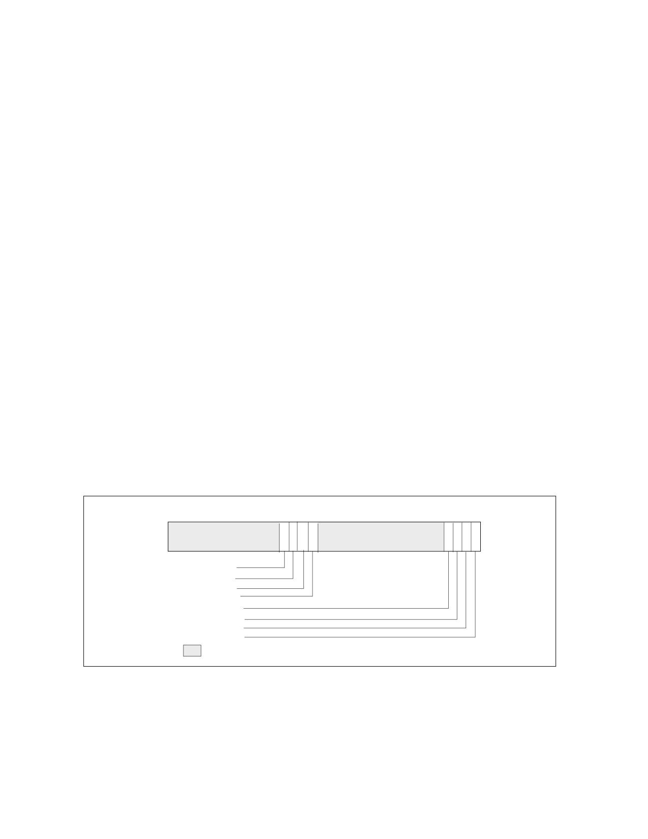
the respective IA32_PMCx overflow condition. The layout of IA32_PEBS_ENABLE for processors based on Nehalem
microarchitecture is shown in Figure 20-15.
When a counter is enabled to capture machine state (PEBS_EN_PMCx = 1), the processor will write machine state
information to a memory buffer specified by software as detailed below. When the counter IA32_PMCx overflows
from maximum count to zero, the PEBS hardware is armed.
63
36 3534
33 32
31
8 7
6
5 4
3
2
1
0
LL_EN_PMC3 (R/W)
LL_EN_PMC2 (R/W)
LL_EN_PMC1 (R/W)
LL_EN_PMC0 (R/W)
PEBS_EN_PMC3 (R/W)
PEBS_EN_PMC2 (R/W)
PEBS_EN_PMC1 (R/W)
PEBS_EN_PMC0 (R/W)
Reserved
RESET Value — 00000000_00000000H
Figure 20-15. Layout of IA32_PEBS_ENABLE MSR
Upon occurrence of the next PEBS event, the PEBS hardware triggers an assist and causes a PEBS record to be
written. The format of the PEBS record is indicated by the bit field IA32_PERF_CAPABILITIES[11:8] (see
Figure 20-65).
Vol. 3B
20-19

PERFORMANCE MONITORING
The behavior of PEBS assists is reported by IA32_PERF_CAPABILITIES[6] (see Figure 20-65). The return instruc-
tion pointer (RIP) reported in the PEBS record will point to the instruction after (+1) the instruction that causes the
PEBS assist. The machine state reported in the PEBS record is the machine state after the instruction that causes
the PEBS assist is retired. For instance, if the instructions:
mov eax, [eax] ; causes PEBS assist
nop
are executed, the PEBS record will report the address of the nop, and the value of EAX in the PEBS record will show
the value read from memory, not the target address of the read operation.
The PEBS record format is shown in Table 20-3, and each field in the PEBS record is 64 bits long. The PEBS record
format, along with debug/store area storage format, does not change regardless of IA-32e mode is active or not.
CPUID.01H:ECX.DTES64[bit 2] reports whether the processor's DS storage format support is mode-independent.
When set, it uses 64-bit DS storage format.
Table 20-3. PEBS Record Format for Intel Core i7 Processor Family
Byte Offset
Field
Byte Offset
Field
00H
R/EFLAGS
58H
R9
08H
R/EIP
60H
R10
10H
R/EAX
68H
R11
18H
R/EBX
70H
R12
20H
R/ECX
78H
R13
28H
R/EDX
80H
R14
30H
R/ESI
88H
R15
38H
R/EDI
90H
IA32_PERF_GLOBAL_STATUS
40H
R/EBP
98H
Data Linear Address
48H
R/ESP
A0H
Data Source Encoding
50H
R8
A8H
Latency value (core cycles)
In IA-32e mode, the full 64-bit value is written to the register. If the processor is not operating in IA-32e mode, 32-
bit value is written to registers with bits 63:32 zeroed. Registers not defined when the processor is not in IA-32e
mode are written to zero.
Bytes AFH:90H are enhancement to the PEBS record format. Support for this enhanced PEBS record format is indi-
cated by IA32_PERF_CAPABILITIES[11:8] encoding of 0001B.
The value written to bytes 97H:90H is the state of the IA32_PERF_GLOBAL_STATUS register before the PEBS assist
occurred. This value is written so software can determine which counters overflowed when this PEBS record was
written. Note that this field indicates the overflow status for all counters, regardless of whether they were
programmed for PEBS or not.
Programming PEBS Facility
Only a subset of non-architectural performance events in the processor support PEBS. The subset of precise events
are listed in Table 20-84. In addition to using IA32_PERFEVTSELx to specify event unit/mask settings and setting
the EN_PMCx bit in the IA32_PEBS_ENABLE register for the respective counter, the software must also initialize the
DS_BUFFER_MANAGEMENT_AREA data structure in memory to support capturing PEBS records for precise events.
The recording of PEBS records may not operate properly if accesses to the linear addresses in the DS buffer
management area or in the PEBS buffer (see below) cause page faults, VM exits, or the setting of accessed or dirty
flags in the paging structures (ordinary or EPT). For that reason, system software should establish paging struc-
tures (both ordinary and EPT) to prevent such occurrences. Implications of this may be that an operating system
should allocate this memory from a non-paged pool and that system software cannot do “lazy” page-table entry
propagation for these pages. A virtual-machine monitor may choose to allow use of PEBS by guest software only if
EPT maps all guest-physical memory as present and read/write.
20-20
Vol. 3B
PERFORMANCE MONITORING
NOTE
PEBS events are only valid when the following fields of IA32_PERFEVTSELx are all zero: AnyThread,
Edge, Invert, CMask.
The beginning linear address of the DS_BUFFER_MANAGEMENT_AREA data structure must be programmed into
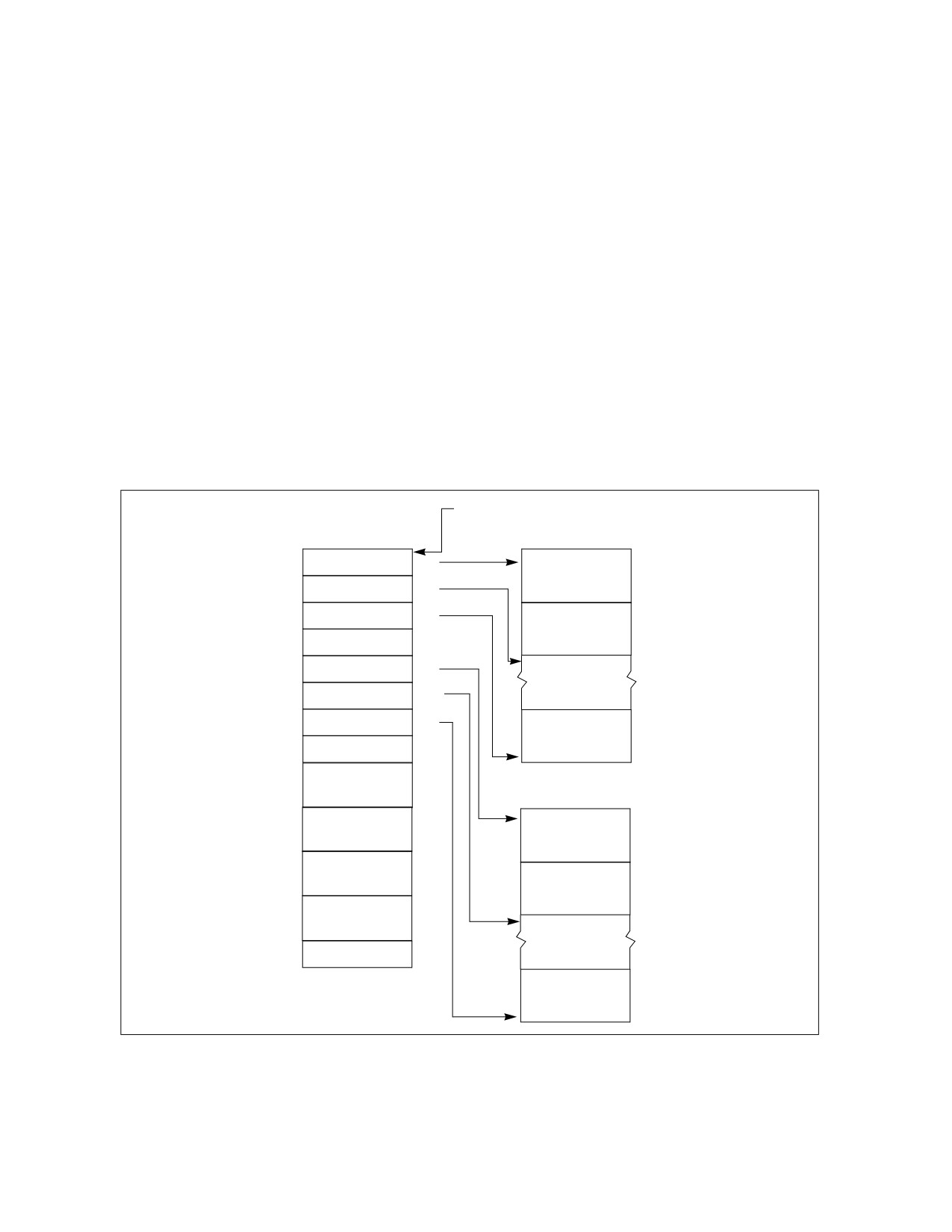
the IA32_DS_AREA register. The layout of the DS_BUFFER_MANAGEMENT_AREA is shown in Figure 20-16.
• PEBS Buffer Base: This field is programmed with the linear address of the first byte of the PEBS buffer
allocated by software. The processor reads this field to determine the base address of the PEBS buffer.
• PEBS Index: This field is initially programmed with the same value as the PEBS Buffer Base field, or the
beginning linear address of the PEBS buffer. The processor reads this field to determine the location of the next
PEBS record to write to. After a PEBS record has been written, the processor also updates this field with the
address of the next PEBS record to be written. The figure above illustrates the state of PEBS Index after the first
PEBS record is written.
• PEBS Absolute Maximum: This field represents the absolute address of the maximum length of the allocated
PEBS buffer plus the starting address of the PEBS buffer. The processor will not write any PEBS record beyond
the end of PEBS buffer, when PEBS Index equals PEBS Absolute Maximum. No signaling is generated when
PEBS buffer is full. Software must reset the PEBS Index field to the beginning of the PEBS buffer address to
continue capturing PEBS records.
IA32_DS_AREA MSR
DS Buffer Management Area
BTS Buffer
BTS Buffer Base
0H
Branch Record 0
BTS Index
8H
BTS Absolute
10H
Maximum
Branch Record 1
BTS Interrupt
18H
Threshold
PEBS Buffer Base
20H
PEBS Index
28H
PEBS Absolute
30H
Maximum
Branch Record n
PEBS Interrupt
38H
Threshold
40H
PEBS
Counter0 Reset
PEBS Buffer
48H
PEBS
Counter1 Reset
PEBS Record 0
50H
PEBS
Counter2 Reset
PEBS Record 1
58H
PEBS
Counter3 Reset
60H
Reserved
PEBS Record n
Figure 20-16. PEBS Programming Environment
Vol. 3B
20-21
PERFORMANCE MONITORING
• PEBS Interrupt Threshold: This field specifies the threshold value to trigger a performance interrupt and
notify software that the PEBS buffer is nearly full. This field is programmed with the linear address of the first
byte of the PEBS record within the PEBS buffer that represents the threshold record. After the processor writes
a PEBS record and updates PEBS Index, if the PEBS Index reaches the threshold value of this field, the
processor will generate a performance interrupt. This is the same interrupt that is generated by a performance
counter overflow, as programmed in the Performance Monitoring Counters vector in the Local Vector Table of
the Local APIC. When a performance interrupt due to PEBS buffer full is generated, the IA32_PERF_-
GLOBAL_STATUS.PEBS_Ovf bit will be set.
• PEBS CounterX Reset: This field allows software to set up PEBS counter overflow condition to occur at a rate
useful for profiling workload, thereby generating multiple PEBS records to facilitate characterizing the profile
the execution of test code. After each PEBS record is written, the processor checks each counter to see if it
overflowed and was enabled for PEBS (the corresponding bit in IA32_PEBS_ENABLED was set). If these
conditions are met, then the reset value for each overflowed counter is loaded from the DS Buffer Management
Area. For example, if counter IA32_PMC0 caused a PEBS record to be written, then the value of “PEBS Counter
0 Reset” would be written to counter IA32_PMC0. If a counter is not enabled for PEBS, its value will not be
modified by the PEBS assist.
Performance Counter Prioritization
Performance monitoring interrupts are triggered by a counter transitioning from maximum count to zero (assuming
IA32_PerfEvtSelX.INT is set). This same transition will cause PEBS hardware to arm, but not trigger. PEBS hard-
ware triggers upon detection of the first PEBS event after the PEBS hardware has been armed (a 0 to 1 transition
of the counter). At this point, a PEBS assist will be undertaken by the processor.
Performance counters (fixed and general-purpose) are prioritized in index order. That is, counter IA32_PMC0 takes
precedence over all other counters. Counter IA32_PMC1 takes precedence over counters IA32_PMC2 and
IA32_PMC3, and so on. This means that if simultaneous overflows or PEBS assists occur, the appropriate action will
be taken for the highest priority performance counter. For example, if IA32_PMC1 cause an overflow interrupt and
IA32_PMC2 causes an PEBS assist simultaneously, then the overflow interrupt will be serviced first.
The PEBS threshold interrupt is triggered by the PEBS assist, and is by definition prioritized lower than the PEBS
assist. Hardware will not generate separate interrupts for each counter that simultaneously overflows. General-
purpose performance counters are prioritized over fixed counters.
If a counter is programmed with a precise (PEBS-enabled) event and programmed to generate a counter overflow
interrupt, the PEBS assist is serviced before the counter overflow interrupt is serviced. If in addition the PEBS inter-
rupt threshold is met, the
threshold interrupt is generated after the PEBS assist completes, followed by the counter overflow interrupt (two
separate interrupts are generated).
Uncore counters may be programmed to interrupt one or more processor cores (see Section 20.3.1.2). It is
possible for interrupts posted from the uncore facility to occur coincident with counter overflow interrupts from the
processor core. Software must check core and uncore status registers to determine the exact origin of counter
overflow interrupts.
20.3.1.1.2 Load Latency Performance Monitoring Facility
The load latency facility provides software a means to characterize the average load latency to different levels of
cache/memory hierarchy. This facility requires processor supporting enhanced PEBS record format in the PEBS
buffer, see Table 20-3. This field measures the load latency from load's first dispatch of till final data writeback from
the memory subsystem. The latency is reported for retired demand load operations and in core cycles (it accounts
for re-dispatches).
To use this feature software must assure:
• One of the IA32_PERFEVTSELx MSR is programmed to specify the event unit MEM_INST_RETIRED, and the
LATENCY_ABOVE_THRESHOLD event mask must be specified (IA32_PerfEvtSelX[15:0] = 100H). The corre-
sponding counter IA32_PMCx will accumulate event counts for architecturally visible loads which exceed the
programmed latency threshold specified separately in a MSR. Stores are ignored when this event is
programmed. The CMASK or INV fields of the IA32_PerfEvtSelX register used for counting load latency must be
0. Writing other values will result in undefined behavior.
20-22
Vol. 3B

PERFORMANCE MONITORING
• The MSR_PEBS_LD_LAT_THRESHOLD MSR is programmed with the desired latency threshold in core clock
cycles. Loads with latencies greater than this value are eligible for counting and latency data reporting. The
minimum value that may be programmed in this register is 3 (the minimum detectable load latency is 4 core
clock cycles).
• The PEBS enable bit in the IA32_PEBS_ENABLE register is set for the corresponding IA32_PMCx counter
register. This means that both the PEBS_EN_CTRX and LL_EN_CTRX bits must be set for the counter(s) of
interest. For example, to enable load latency on counter IA32_PMC0, the IA32_PEBS_ENABLE register must be
programmed with the 64-bit value 00000001_00000001H.
When the load-latency facility is enabled, load operations are randomly selected by hardware and tagged to carry
information related to data source locality and latency. Latency and data source information of tagged loads are
updated internally.
When a PEBS assist occurs, the last update of latency and data source information are captured by the assist and
written as part of the PEBS record. The PEBS sample after value (SAV), specified in PEBS CounterX Reset, operates
orthogonally to the tagging mechanism. Loads are randomly tagged to collect latency data. The SAV controls the
number of tagged loads with latency information that will be written into the PEBS record field by the PEBS assists.
The load latency data written to the PEBS record will be for the last tagged load operation which retired just before
the PEBS assist was invoked.
The load-latency information written into a PEBS record (see Table 20-3, bytes AFH:98H) consists of:
• Data Linear Address: This is the linear address of the target of the load operation.
• Latency Value: This is the elapsed cycles of the tagged load operation between dispatch to GO, measured in
processor core clock domain.
• Data Source: The encoded value indicates the origin of the data obtained by the load instruction. The
encoding is shown in Table 20-4. In the descriptions, local memory refers to system memory physically
attached to a processor package, and remote memory refers to system memory physically attached to another
processor package.
Table 20-4. Data Source Encoding for Load Latency Record
Encoding
Description
00H
Unknown L3 cache miss.
01H
Minimal latency core cache hit. This request was satisfied by the L1 data cache.
02H
Pending core cache HIT. Outstanding core cache miss to same cache-line address was already underway.
03H
This data request was satisfied by the L2.
04H
L3 HIT. Local or Remote home requests that hit L3 cache in the uncore with no coherency actions required (snooping).
05H
L3 HIT. Local or Remote home requests that hit the L3 cache and were serviced by another processor core with a
cross core snoop where no modified copies were found. (clean).
06H
L3 HIT. Local or Remote home requests that hit the L3 cache and were serviced by another processor core with a
cross core snoop where no modified copies were found.
07H1
Reserved/LLC Snoop HitM. Local or Remote home requests that hit the last level cache and were serviced by another
core with a cross core snoop where modified copies were found.
08H
Reserved/L3 MISS. Local homed requests that missed the L3 cache and were serviced by forwarded data following a
cross package snoop where no modified copies were found. (Remote home requests are not counted).
09H
Reserved
0AH
L3 MISS. Local home requests that missed the L3 cache and were serviced by local DRAM (go to shared state).
0BH
L3 MISS. Remote home requests that missed the L3 cache and were serviced by remote DRAM (go to shared state).
0CH
L3 MISS. Local home requests that missed the L3 cache and were serviced by local DRAM (go to exclusive state).
0DH
L3 MISS. Remote home requests that missed the L3 cache and were serviced by remote DRAM (go to exclusive state).
0EH
I/O, Request of input/output operation.
0FH
The request was to un-cacheable memory.
Vol. 3B
20-23

PERFORMANCE MONITORING
NOTES:
1. Bit 7 is supported only for processors with a CPUID DisplayFamily_DisplayModel signature of 06_2A, and 06_2E; otherwise it is
reserved.
The layout of MSR_PEBS_LD_LAT_THRESHOLD is shown in Figure 20-17.
63
1615
0
THRHLD - Load latency threshold
Reserved
RESET Value — 00000000_00000000H
Figure 20-17. Layout of MSR_PEBS_LD_LAT MSR
Bits 15:0 specifies the threshold load latency in core clock cycles. Performance events with latencies greater than
this value are counted in IA32_PMCx and their latency information is reported in the PEBS record. Otherwise, they
are ignored. The minimum value that may be programmed in this field is 3.
20.3.1.1.3 Off-core Response Performance Monitoring in the Processor Core
Programming a performance event using the off-core response facility can choose any of the four IA32_PERFEVT-
SELx MSR with specific event codes and predefine mask bit value. Each event code for off-core response monitoring
requires programming an associated configuration MSR, MSR_OFFCORE_RSP_0. There is only one off-core
response configuration MSR. Table 20-5 lists the event code, mask value and additional off-core configuration MSR
that must be programmed to count off-core response events using IA32_PMCx.
Table 20-5. Off-Core Response Event Encoding
Event code in
Mask Value in
IA32_PERFEVTSELx
IA32_PERFEVTSELx
Required Off-core Response MSR
B7H
01H
MSR_OFFCORE_RSP_0 (address 1A6H)
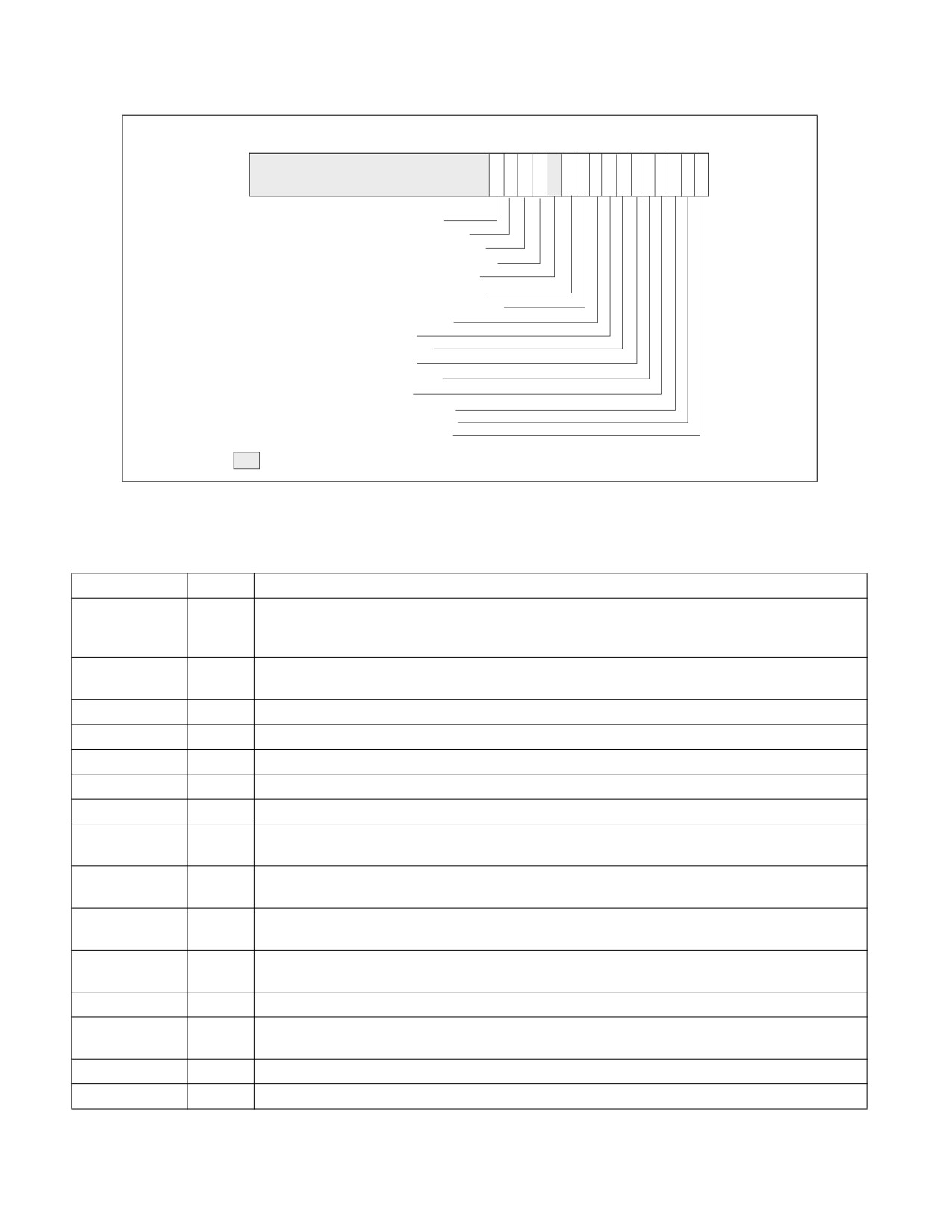
The layout of MSR_OFFCORE_RSP_0 is shown in Figure 20-18. Bits 7:0 specifies the request type of a transaction
request to the uncore. Bits 15:8 specifies the response of the uncore subsystem.
20-24
Vol. 3B
PERFORMANCE MONITORING
63
15 14 1312 11
10
9
8 7
6
5
4
3
2
1
0
RESPONSE TYPE — NON_DRAM (R/W)
RESPONSE TYPE — LOCAL_DRAM (R/W)
RESPONSE TYPE — REMOTE_DRAM (R/W)
RESPONSE TYPE — REMOTE_CACHE_FWD (R/W)
RESPONSE TYPE — RESERVED
RESPONSE TYPE — OTHER_CORE_HITM (R/W)
RESPONSE TYPE — OTHER_CORE_HIT_SNP (R/W)
RESPONSE TYPE — UNCORE_HIT (R/W)
REQUEST TYPE — OTHER (R/W)
REQUEST TYPE — PF_IFETCH (R/W)
REQUEST TYPE — PF_RFO (R/W)
REQUEST TYPE — PF_DATA_RD (R/W)
REQUEST TYPE — WB (R/W)
REQUEST TYPE — DMND_IFETCH (R/W)
REQUEST TYPE — DMND_RFO (R/W)
REQUEST TYPE — DMND_DATA_RD (R/W)
Reserved
RESET Value — 00000000_00000000H
Figure 20-18. Layout of MSR_OFFCORE_RSP_0 and MSR_OFFCORE_RSP_1 to Configure Off-core Response Events
Table 20-6. MSR_OFFCORE_RSP_0 and MSR_OFFCORE_RSP_1 Bit Field Definition
Bit Name
Offset
Description
DMND_DATA_RD
0
Counts the number of demand and DCU prefetch data reads of full and partial cachelines as well as
demand data page table entry cacheline reads. Does not count L2 data read prefetches or instruction
fetches.
DMND_RFO
1
Counts the number of demand and DCU prefetch reads for ownership (RFO) requests generated by a
write to data cacheline. Does not count L2 RFO.
DMND_IFETCH
2
Counts the number of demand instruction cacheline reads and L1 instruction cacheline prefetches.
WB
3
Counts the number of writeback (modified to exclusive) transactions.
PF_DATA_RD
4
Counts the number of data cacheline reads generated by L2 prefetchers.
PF_RFO
5
Counts the number of RFO requests generated by L2 prefetchers.
PF_IFETCH
6
Counts the number of code reads generated by L2 prefetchers.
OTHER
7
Counts one of the following transaction types, including L3 invalidate, I/O, full or partial writes, WC or
non-temporal stores, CLFLUSH, Fences, lock, unlock, split lock.
UNCORE_HIT
8
L3 Hit: local or remote home requests that hit L3 cache in the uncore with no coherency actions
required (snooping).
OTHER_CORE_HI
9
L3 Hit: local or remote home requests that hit L3 cache in the uncore and was serviced by another
T_SNP
core with a cross core snoop where no modified copies were found (clean).
OTHER_CORE_HI
10
L3 Hit: local or remote home requests that hit L3 cache in the uncore and was serviced by another
TM
core with a cross core snoop where modified copies were found (HITM).
Reserved
11
Reserved
REMOTE_CACHE_
12
L3 Miss: local homed requests that missed the L3 cache and was serviced by forwarded data following
FWD
a cross package snoop where no modified copies found. (Remote home requests are not counted)
REMOTE_DRAM
13
L3 Miss: remote home requests that missed the L3 cache and were serviced by remote DRAM.
LOCAL_DRAM
14
L3 Miss: local home requests that missed the L3 cache and were serviced by local DRAM.
Vol. 3B
20-25

PERFORMANCE MONITORING
Table 20-6. MSR_OFFCORE_RSP_0 and MSR_OFFCORE_RSP_1 Bit Field Definition (Contd.)
Bit Name
Offset
Description
NON_DRAM
15
Non-DRAM requests that were serviced by IOH.
20.3.1.2 Performance Monitoring Facility in the Uncore
The “uncore” in Nehalem microarchitecture refers to subsystems in the physical processor package that are shared
by multiple processor cores. Some of the sub-systems in the uncore include the L3 cache, Intel QuickPath Intercon-
nect link logic, and integrated memory controller. The performance monitoring facilities inside the uncore operates
in the same clock domain as the uncore (U-clock domain), which is usually different from the processor core clock
domain. The uncore performance monitoring facilities described in this section apply to Intel Xeon processor 5500
series and processors with the following CPUID signatures: 06_1AH, 06_1EH, 06_1FH (see Chapter 2, “Model-
Specific Registers (MSRs),” in the Intel® 64 and IA-32 Architectures Software Developer’s Manual, Volume 4). An
overview of the uncore performance monitoring facilities is described separately.
The performance monitoring facilities available in the U-clock domain consist of:
• Eight General-purpose counters (MSR_UNCORE_PerfCntr0 through MSR_UNCORE_PerfCntr7). The counters
are 48 bits wide. Each counter is associated with a configuration MSR, MSR_UNCORE_PerfEvtSelx, to specify
event code, event mask and other event qualification fields. A set of global uncore performance counter
enabling/overflow/status control MSRs are also provided for software.
• Performance monitoring in the uncore provides an address/opcode match MSR that provides event qualification
control based on address value or QPI command opcode.
• One fixed-function counter, MSR_UNCORE_FixedCntr0. The fixed-function uncore counter increments at the
rate of the U-clock when enabled.
The frequency of the uncore clock domain can be determined from the uncore clock ratio which is available in
the PCI configuration space register at offset C0H under device number 0 and Function 0.
20.3.1.2.1 Uncore Performance Monitoring Management Facility
MSR_UNCORE_PERF_GLOBAL_CTRL provides bit fields to enable/disable general-purpose and fixed-function
counters in the uncore. Figure 20-19 shows the layout of MSR_UNCORE_PERF_GLOBAL_CTRL for an uncore that is
shared by four processor cores in a physical package.
• EN_PCn (bit n, n = 0, 7): When set, enables counting for the general-purpose uncore counter MSR_UN-
CORE_PerfCntr n.
• EN_FC0 (bit 32): When set, enables counting for the fixed-function uncore counter MSR_UNCORE_FixedCntr0.
• EN_PMI_COREn (bit n, n = 0, 3 if four cores are present): When set, processor core n is programmed to receive
an interrupt signal from any interrupt enabled uncore counter. PMI delivery due to an uncore counter overflow
is enabled by setting IA32_DEBUGCTL.Offcore_PMI_EN to 1.
• PMI_FRZ (bit 63): When set, all U-clock uncore counters are disabled when any one of them signals a
performance interrupt. Software must explicitly re-enable the counter by setting the enable bits in MSR_UN-
CORE_PERF_GLOBAL_CTRL upon exit from the ISR.
20-26
Vol. 3B

PERFORMANCE MONITORING
63 62
51 50 4948
32
31
8 7
6
5 4
3
2
1
0
PMI_FRZ (R/W)
EN_PMI_CORE3 (R/W)
EN_PMI_CORE2 (R/W)
EN_PMI_CORE1 (R/W)
EN_PMI_CORE0 (R/W)
EN_FC0 (R/W)
EN_PC7 (R/W)
EN_PC6 (R/W)
EN_PC5 (R/W)
EN_PC4 (R/W)
EN_PC3 (R/W)
EN_PC2 (R/W)
EN_PC1 (R/W)
EN_PC0 (R/W)
Reserved
RESET Value — 00000000_00000000H
Figure 20-19. Layout of MSR_UNCORE_PERF_GLOBAL_CTRL MSR
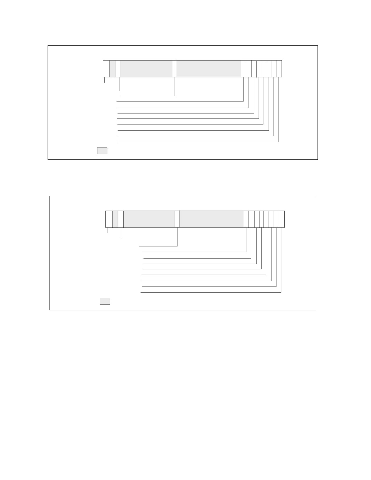
MSR_UNCORE_PERF_GLOBAL_STATUS provides overflow status of the U-clock performance counters in the
uncore. This is a read-only register. If an overflow status bit is set the corresponding counter has overflowed. The
register provides a condition change bit (bit 63) which can be quickly checked by software to determine if a signif-
icant change has occurred since the last time the condition change status was cleared. Figure 20-20 shows the
layout of MSR_UNCORE_PERF_GLOBAL_STATUS.
• OVF_PCn (bit n, n = 0, 7): When set, indicates general-purpose uncore counter MSR_UNCORE_PerfCntr n has
overflowed.
• OVF_FC0 (bit 32): When set, indicates the fixed-function uncore counter MSR_UNCORE_FixedCntr0 has
overflowed.
• OVF_PMI (bit 61): When set indicates that an uncore counter overflowed and generated an interrupt request.
• CHG (bit 63): When set indicates that at least one status bit in MSR_UNCORE_PERF_GLOBAL_STATUS register
has changed state.
MSR_UNCORE_PERF_GLOBAL_OVF_CTRL allows software to clear the status bits in the UNCORE_PERF_-
GLOBAL_STATUS register. This is a write-only register, and individual status bits in the global status register are
cleared by writing a binary one to the corresponding bit in this register. Writing zero to any bit position in this
register has no effect on the uncore PMU hardware.
Vol. 3B
20-27
PERFORMANCE MONITORING
63 62 6160
32
31
8 7
6
5 4
3
2
1
0
CHG (R/W)
OVF_PMI (R/W)
OVF_FC0 (R/O)
OVF_PC7 (R/O)
OVF_PC6 (R/O)
OVF_PC5 (R/O)
OVF_PC4 (R/O)
OVF_PC3 (R/O)
OVF_PC2 (R/O)
OVF_PC1 (R/O)
OVF_PC0 (R/O)
Reserved
RESET Value — 00000000_00000000H
Figure 20-20. Layout of MSR_UNCORE_PERF_GLOBAL_STATUS MSR
Figure 20-21 shows the layout of MSR_UNCORE_PERF_GLOBAL_OVF_CTRL.
63 62 6160
32
31
8 7
6
5 4
3
2
1
0
CLR_CHG (WO1)
CLR_OVF_PMI (WO1)
CLR_OVF_FC0 (WO1)
CLR_OVF_PC7 (WO1)
CLR_OVF_PC6 (WO1)
CLR_OVF_PC5 (WO1)
CLR_OVF_PC4 (WO1)
CLR_OVF_PC3 (WO1)
CLR_OVF_PC2 (WO1)
CLR_OVF_PC1 (WO1)
CLR_OVF_PC0 (WO1)
Reserved
RESET Value — 00000000_00000000H
Figure 20-21. Layout of MSR_UNCORE_PERF_GLOBAL_OVF_CTRL MSR
• CLR_OVF_PCn (bit n, n = 0, 7): Set this bit to clear the overflow status for general-purpose uncore counter
MSR_UNCORE_PerfCntr n. Writing a value other than 1 is ignored.
• CLR_OVF_FC0 (bit 32): Set this bit to clear the overflow status for the fixed-function uncore counter MSR_UN-
CORE_FixedCntr0. Writing a value other than 1 is ignored.
• CLR_OVF_PMI (bit 61): Set this bit to clear the OVF_PMI flag in MSR_UNCORE_PERF_GLOBAL_STATUS. Writing
a value other than 1 is ignored.
• CLR_CHG (bit 63): Set this bit to clear the CHG flag in MSR_UNCORE_PERF_GLOBAL_STATUS register. Writing
a value other than 1 is ignored.
20.3.1.2.2 Uncore Performance Event Configuration Facility
MSR_UNCORE_PerfEvtSel0 through MSR_UNCORE_PerfEvtSel7 are used to select performance event and
configure the counting behavior of the respective uncore performance counter. Each uncore PerfEvtSel MSR is
paired with an uncore performance counter. Each uncore counter must be locally configured using the corre-
20-28
Vol. 3B
PERFORMANCE MONITORING
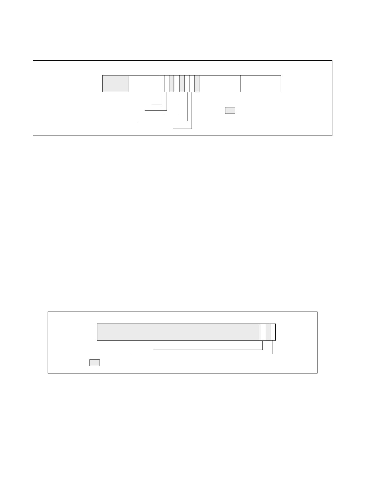
sponding MSR_UNCORE_PerfEvtSelx and counting must be enabled using the respective EN_PCx bit in MSR_UN-
CORE_PERF_GLOBAL_CTRL. Figure 20-22 shows the layout of MSR_UNCORE_PERFEVTSELx.
63
31
2423222120191817 16 15
8 7
0
Counter Mask
Unit Mask (UMASK)
Event Select
(CMASK)
INV—Invert counter mask
EN—Enable counters
Reserved
PMI—Enable PMI on overflow
E—Edge detect
RESET Value — 00000000_00000000H
OCC_CTR_RST—Rest Queue Occ
Figure 20-22. Layout of MSR_UNCORE_PERFEVTSELx MSRs
•
Event Select (bits 7:0): Selects the event logic unit used to detect uncore events.
•
Unit Mask (bits 15:8) : Condition qualifiers for the event selection logic specified in the Event Select field.
•
OCC_CTR_RST (bit17): When set causes the queue occupancy counter associated with this event to be cleared
(zeroed). Writing a zero to this bit will be ignored. It will always read as a zero.
•
Edge Detect (bit 18): When set causes the counter to increment when a deasserted to asserted transition
occurs for the conditions that can be expressed by any of the fields in this register.
•
PMI (bit 20): When set, the uncore will generate an interrupt request when this counter overflowed. This
request will be routed to the logical processors as enabled in the PMI enable bits (EN_PMI_COREx) in the
register MSR_UNCORE_PERF_GLOBAL_CTRL.
•
EN (bit 22): When clear, this counter is locally disabled. When set, this counter is locally enabled and counting
starts when the corresponding EN_PCx bit in MSR_UNCORE_PERF_GLOBAL_CTRL is set.
•
INV (bit 23): When clear, the Counter Mask field is interpreted as greater than or equal to. When set, the
Counter Mask field is interpreted as less than.
•
Counter Mask (bits 31:24): When this field is clear, it has no effect on counting. When set to a value other than
zero, the logical processor compares this field to the event counts on each core clock cycle. If INV is clear and
the event counts are greater than or equal to this field, the counter is incremented by one. If INV is set and the
event counts are less than this field, the counter is incremented by one. Otherwise the counter is not incre-
mented.
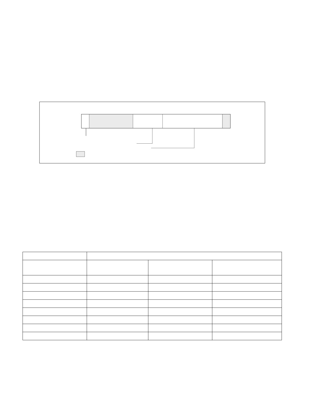
Figure 20-23 shows the layout of MSR_UNCORE_FIXED_CTR_CTRL.
63
8 7
6
5 4
3
2
1
0
PMI - Generate PMI on overflow
EN - Enable
Reserved
RESET Value — 00000000_00000000H
Figure 20-23. Layout of MSR_UNCORE_FIXED_CTR_CTRL MSR
• EN (bit 0): When clear, the uncore fixed-function counter is locally disabled. When set, it is locally enabled and
counting starts when the EN_FC0 bit in MSR_UNCORE_PERF_GLOBAL_CTRL is set.
• PMI (bit 2): When set, the uncore will generate an interrupt request when the uncore fixed-function counter
overflowed. This request will be routed to the logical processors as enabled in the PMI enable bits
(EN_PMI_COREx) in the register MSR_UNCORE_PERF_GLOBAL_CTRL.
Vol. 3B
20-29
PERFORMANCE MONITORING
Both the general-purpose counters (MSR_UNCORE_PerfCntr) and the fixed-function counter (MSR_UNCORE_-
FixedCntr0) are 48 bits wide. They support both counting and interrupt based sampling usages. The event logic
unit can filter event counts to specific regions of code or transaction types incoming to the home node logic.
20.3.1.2.3 Uncore Address/Opcode Match MSR
The Event Select field [7:0] of MSR_UNCORE_PERFEVTSELx is used to select different uncore event logic unit.
When the event “ADDR_OPCODE_MATCH” is selected in the Event Select field, software can filter uncore perfor-
mance events according to transaction address and certain transaction responses. The address filter and transac-
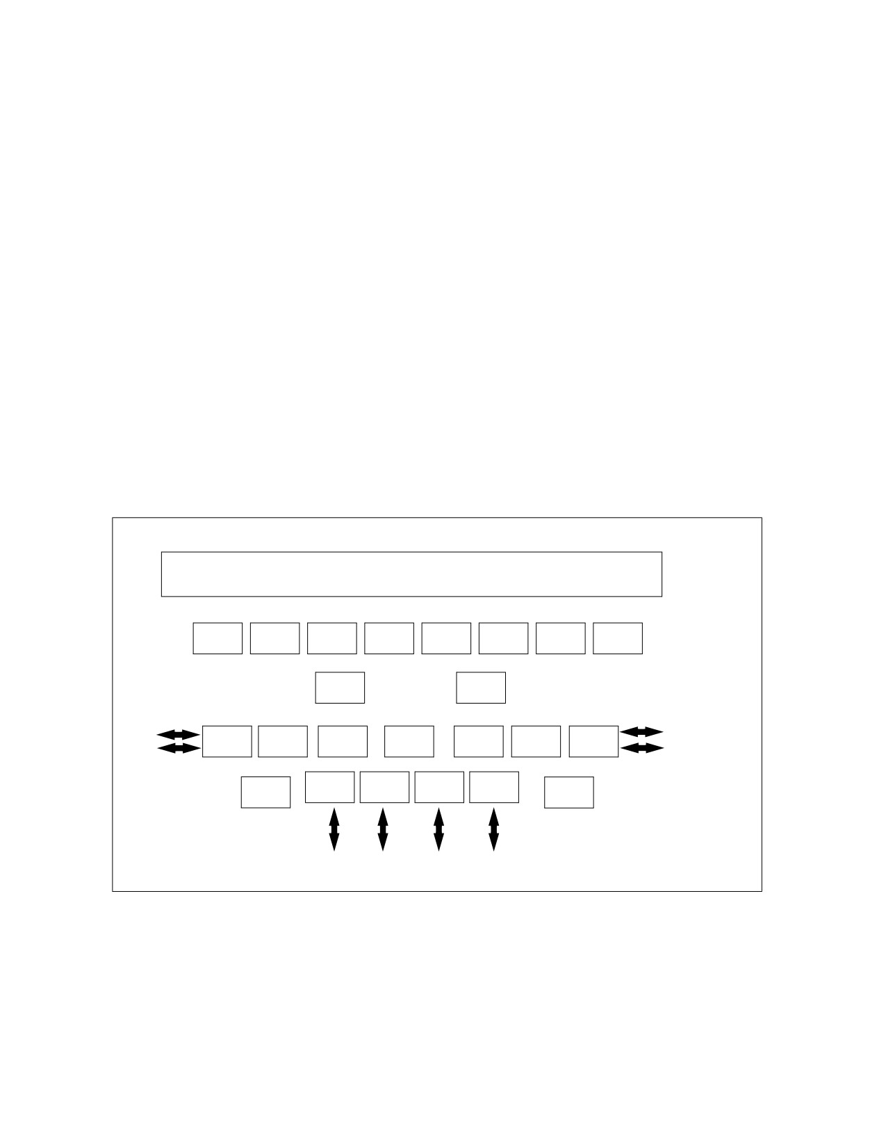
tion response filtering requires the use of MSR_UNCORE_ADDR_OPCODE_MATCH register. The layout is shown in
Figure 20-24.
63
60
4847
4039
3 2 0
Opcode
ADDR
MatchSel—Select addr/Opcode
Opcode—Opcode and Message
ADDR—Bits 39:4 of physical address
Reserved
RESET Value — 00000000_00000000H
Figure 20-24. Layout of MSR_UNCORE_ADDR_OPCODE_MATCH MSR
• Addr (bits 39:3): The physical address to match if “MatchSel“ field is set to select address match. The uncore
performance counter will increment if the lowest 40-bit incoming physical address (excluding bits 2:0) for a
transaction request matches bits 39:3.
• Opcode (bits 47:40) : Bits 47:40 allow software to filter uncore transactions based on QPI link message
class/packed header opcode. These bits are consists two sub-fields:
— Bits 43:40 specify the QPI packet header opcode.
— Bits 47:44 specify the QPI message classes.
Table 20-7 lists the encodings supported in the opcode field.
Table 20-7. Opcode Field Encoding for MSR_UNCORE_ADDR_OPCODE_MATCH
Opcode [43:40]
QPI Message Class
Home Request
Snoop Response
Data Response
[47:44] = 0000B
[47:44] = 0001B
[47:44] = 1110B
1
DMND_IFETCH
2
2
WB
3
3
PF_DATA_RD
4
4
PF_RFO
5
5
PF_IFETCH
6
6
OTHER
7
7
NON_DRAM
15
15
20-30
Vol. 3B
PERFORMANCE MONITORING
• MatchSel (bits 63:61): Software specifies the match criteria according to the following encoding:
— 000B: Disable addr_opcode match hardware.
— 100B: Count if only the address field matches.
— 010B: Count if only the opcode field matches.
— 110B: Count if either opcode field matches or the address field matches.
— 001B: Count only if both opcode and address field match.
— Other encoding are reserved.
20.3.1.3 Intel® Xeon® Processor 7500 Series Performance Monitoring Facility
The performance monitoring facility in the processor core of Intel® Xeon® processor 7500 series are the same as
those supported in Intel Xeon processor 5500 series. The uncore subsystem in Intel Xeon processor 7500 series
are significantly different The uncore performance monitoring facility consist of many distributed units associated
with individual logic control units (referred to as boxes) within the uncore subsystem. A high level block diagram of
the various box units of the uncore is shown in Figure 20-25.
Uncore PMUs are programmed via MSR interfaces. Each of the distributed uncore PMU units have several general-
purpose counters. Each counter requires an associated event select MSR, and may require additional MSRs to
configure sub-event conditions. The uncore PMU MSRs associated with each box can be categorized based on its
functional scope: per-counter, per-box, or global across the uncore. The number counters available in each box
type are different. Each box generally provides a set of MSRs to enable/disable, check status/overflow of multiple
counters within each box.
L3 Cache
CBox
CBox
CBox
CBox
CBox
CBox
CBox
CBox
SBox
SBox
SMI Channels
PBox
MBox
BBox
RBox
BBox
MBox
PBox
SMI Channels
PBox
PBox
PBox
PBox
WBox
UBox
4 Intel QPI Links
Figure 20-25. Distributed Units of the Uncore of Intel® Xeon® Processor 7500 Series
Table 20-8 summarizes the number MSRs for uncore PMU for each box.
Vol. 3B
20-31

PERFORMANCE MONITORING
Table 20-8. Uncore PMU MSR Summary
Counter
General
Global
Box
# of Boxes
Counters per Box
Width
Purpose
Enable
Sub-control MSRs
C-Box
8
6
48
Yes
per-box
None
S-Box
2
4
48
Yes
per-box
Match/Mask
B-Box
2
4
48
Yes
per-box
Match/Mask
M-Box
2
6
48
Yes
per-box
Yes
R-Box
1
16 ( 2 port, 8 per port)
48
Yes
per-box
Yes
W-Box
1
4
48
Yes
per-box
None
1
48
No
per-box
None
U-Box
1
1
48
Yes
uncore
None
The W-Box provides 4 general-purpose counters, each requiring an event select configuration MSR, similar to the
general-purpose counters in other boxes. There is also a fixed-function counter that increments clockticks in the
uncore clock domain.
For C,S,B,M,R, and W boxes, each box provides an MSR to enable/disable counting, configuring PMI of multiple
counters within the same box, this is somewhat similar the “global control“ programming interface, IA32_PERF_-
GLOBAL_CTRL, offered in the core PMU. Similarly status information and counter overflow control for multiple
counters within the same box are also provided in C,S,B,M,R, and W boxes.
In the U-Box, MSR_U_PMON_GLOBAL_CTL provides overall uncore PMU enable/disable and PMI configuration
control. The scope of status information in the U-box is at per-box granularity, in contrast to the per-box status
information MSR (in the C,S,B,M,R, and W boxes) providing status information of individual counter overflow. The
difference in scope also apply to the overflow control MSR in the U-Box versus those in the other Boxes.
The individual MSRs that provide uncore PMU interfaces are listed in Chapter 2, “Model-Specific Registers (MSRs),”
in the Intel® 64 and IA-32 Architectures Software Developer’s Manual, Volume 4, Table 2-17 under the general
naming style of MSR_%box#%_PMON_%scope_function%, where %box#% designates the type of box and zero-
based index if there are more the one box of the same type, %scope_function% follows the examples below:
• Multi-counter enabling MSRs: MSR_U_PMON_GLOBAL_CTL, MSR_S0_PMON_BOX_CTL, MSR_C7_PMON_-
BOX_CTL, etc.
• Multi-counter status MSRs: MSR_U_PMON_GLOBAL_STATUS, MSR_S0_PMON_BOX_STATUS, MSR_C7_P-
MON_BOX_STATUS, etc.
• Multi-counter overflow control MSRs: MSR_U_PMON_GLOBAL_OVF_CTL, MSR_S0_PMON_BOX_OVF_CTL,
MSR_C7_PMON_BOX_OVF_CTL, etc.
• Performance counters MSRs: the scope is implicitly per counter, e.g., MSR_U_PMON_CTR, MSR_S0_P-
MON_CTR0, MSR_C7_PMON_CTR5, etc.
• Event select MSRs: the scope is implicitly per counter, e.g., MSR_U_PMON_EVNT_SEL, MSR_S0_P-
MON_EVNT_SEL0, MSR_C7_PMON_EVNT_SEL5, etc.
• Sub-control MSRs: the scope is implicitly per-box granularity, e.g., MSR_M0_PMON_TIMESTAMP, MSR_R0_P-
MON_IPERF0_P1, MSR_S1_PMON_MATCH.
Details of uncore PMU MSR bit field definitions can be found in a separate document “Intel Xeon Processor 7500
Series Uncore Performance Monitoring Guide“.
20.3.2 Performance Monitoring for Processors Based on Westmere Microarchitecture
All of the performance monitoring programming interfaces (architectural and non-architectural core PMU facilities,
and uncore PMU) described in Section 20.6.3 also apply to processors based on Westmere microarchitecture.
Table 20-5 describes a non-architectural performance monitoring event (event code 0B7H) and associated
MSR_OFFCORE_RSP_0 (address 1A6H) in the core PMU. This event and a second functionally equivalent offcore
20-32
Vol. 3B

PERFORMANCE MONITORING
response event using event code 0BBH and MSR_OFFCORE_RSP_1 (address 1A7H) are supported in processors
based on Westmere microarchitecture. The event code and event mask definitions of non-architectural perfor-
mance monitoring events can be found at: https://perfmon-events.intel.com/.
The load latency facility is the same as described in Section 20.3.1.1.2, but added enhancement to provide more
information in the data source encoding field of each load latency record. The additional information relates to
STLB_MISS and LOCK, see Table 20-13.
20.3.3 Intel® Xeon® Processor E7 Family Performance Monitoring Facility
The performance monitoring facility in the processor core of the Intel® Xeon® processor E7 family is the same as
those supported in the Intel Xeon processor 5600 series1. The uncore subsystem in the Intel Xeon processor E7
family is similar to those of the Intel Xeon processor 7500 series. The high level construction of the uncore sub-
system is similar to that shown in Figure 20-25, with the additional capability that up to 10 C-Box units are
supported.
Table 20-9 summarizes the number MSRs for uncore PMU for each box.
Table 20-9. Uncore PMU MSR Summary for Intel® Xeon® Processor E7 Family
Counter
General
Global
Box
# of Boxes
Counters per Box
Width
Purpose
Enable
Sub-control MSRs
C-Box
10
6
48
Yes
per-box
None
S-Box
2
4
48
Yes
per-box
Match/Mask
B-Box
2
4
48
Yes
per-box
Match/Mask
M-Box
2
6
48
Yes
per-box
Yes
R-Box
1
16 ( 2 port, 8 per port)
48
Yes
per-box
Yes
W-Box
1
4
48
Yes
per-box
None
1
48
No
per-box
None
U-Box
1
1
48
Yes
uncore
None
Details of the uncore performance monitoring facility of Intel Xeon Processor E7 family is available in the “Intel®
Xeon® Processor E7 Uncore Performance Monitoring Programming Reference Manual”.
20.3.4 Performance Monitoring for Processors Based on Sandy Bridge Microarchitecture
Intel® Core™ i7-2xxx, Intel® Core™ i5-2xxx, Intel® Core™ i3-2xxx processor series, and Intel® Xeon® processor
E3-1200 family are based on Sandy Bridge microarchitecture; this section describes the performance monitoring
facilities provided in the processor core. The core PMU supports architectural performance monitoring capability
with version ID 3 (see Section 20.2.3) and a host of non-architectural monitoring capabilities.
Architectural performance monitoring version 3 capabilities are described in Section 20.2.3.
The core PMU’s capability is similar to those described in Section 20.3.1.1 and Section 20.6.3, with some differ-
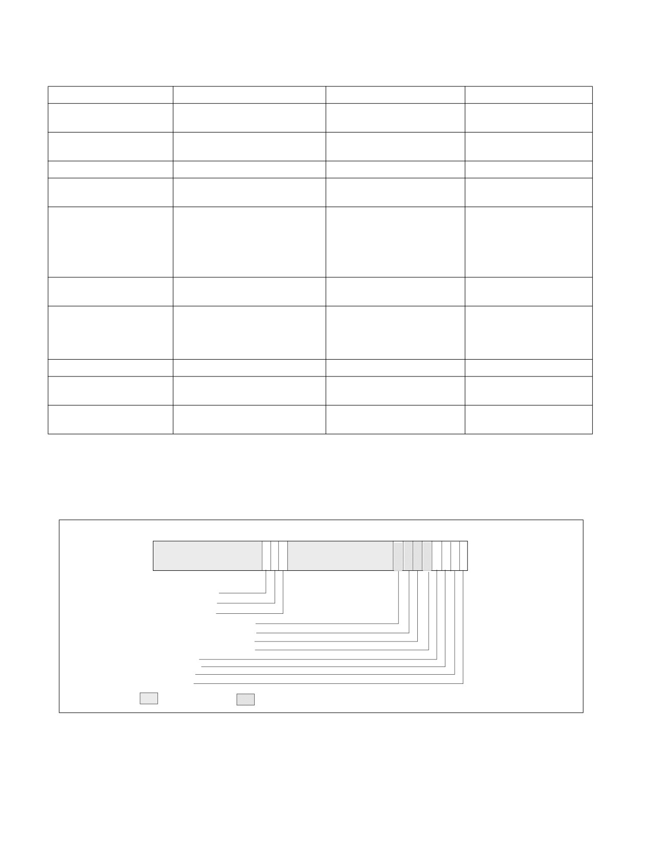
ences and enhancements relative to Westmere microarchitecture summarized in Table 20-10.
1. Exceptions are indicated for event code 0FH in the event list for this processor (https://perfmon-events.intel.com/ ); and valid
bits of data source encoding field of each load latency record is limited to bits 5:4 of Table 20-13.
Vol. 3B
20-33
PERFORMANCE MONITORING
Table 20-10. Core PMU Comparison
Box
Sandy Bridge Microarchitecture
Westmere Microarchitecture
Comment
# of Fixed counters per
3
3
Use CPUID to determine # of
thread
counters. See Section 20.2.1.
# of general-purpose
8
8
Use CPUID to determine # of
counters per core
counters. See Section 20.2.1.
Counter width (R,W)
R:48, W: 32/48
R:48, W:32
See Section 20.2.2.
# of programmable counters
4 or (8 if a core not shared by two
4
Use CPUID to determine # of
per thread
threads)
counters. See Section 20.2.1.
PMI Overhead Mitigation
• Freeze_Perfmon_on_PMI with
• Freeze_Perfmon_on_PMI
See Section 18.4.7.
legacy semantics.
with legacy semantics.
• Freeze_LBR_on_PMI with legacy
• Freeze_LBR_on_PMI with
semantics for branch profiling.
legacy semantics for branch
• Freeze_while_SMM.
profiling.
• Freeze_while_SMM.
Processor Event Based
See Table 20-12.
See Table 20-84.
IA32_PMC4-IA32_PMC7 do
Sampling (PEBS) Events
not support PEBS.
PEBS-Load Latency
See Section 20.3.4.4.2;
Data source encoding
• Data source encoding
• STLB miss encoding
• Lock transaction encoding
PEBS-Precise Store
Section 20.3.4.4.3
No
PEBS-PDIR
Yes (using precise
No
INST_RETIRED.ALL).
Off-core Response Event
MSR 1A6H and 1A7H, extended
MSR 1A6H and 1A7H, limited
Nehalem supports 1A6H
request and response types.
response types.
only.
20.3.4.1 Global Counter Control Facilities in Sandy Bridge Microarchitecture
The number of general-purpose performance counters visible to a logical processor can vary across Processors
based on Sandy Bridge microarchitecture. Software must use CPUID to determine the number performance
counters/event select registers (See Section 20.2.1.1).
63
3534333231
87
6 5
4 3
2 10
FIXED_CTR2 enable
FIXED_CTR1 enable
FIXED_CTR0 enable
PMC7_EN (if PMC7 present)
PMC6_EN (if PMC6 present)
PMC5_EN (if PMC5 present)
PMC4_EN (if PMC4 present)
PMC3_EN
PMC2_EN
PMC1_EN
PMC0_EN
Reserved
Valid if CPUID.0AH:EAX[15:8] = 8, else reserved.
Figure 20-26. IA32_PERF_GLOBAL_CTRL MSR in Sandy Bridge Microarchitecture
20-34
Vol. 3B
PERFORMANCE MONITORING
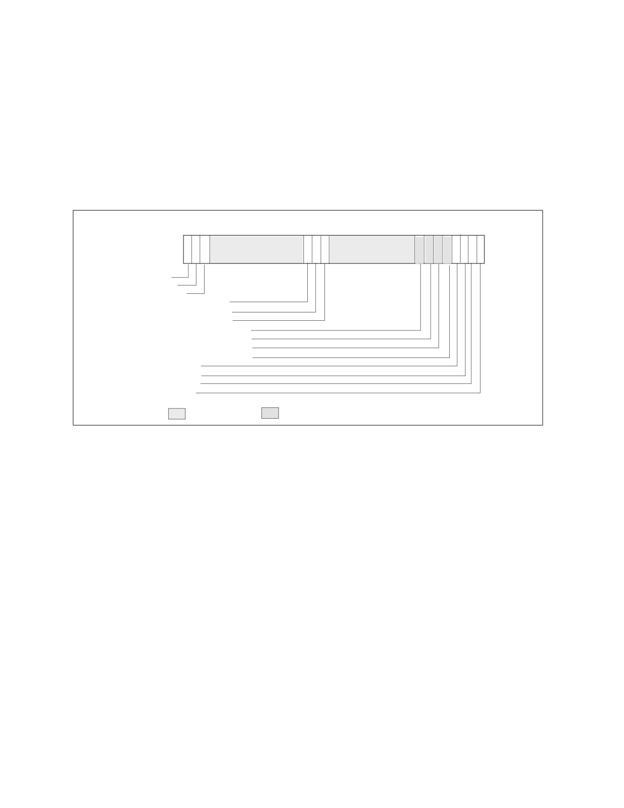
Figure 20-44 depicts the layout of IA32_PERF_GLOBAL_CTRL MSR. The enable bits (PMC4_EN, PMC5_EN,
PMC6_EN, PMC7_EN) corresponding to IA32_PMC4-IA32_PMC7 are valid only if CPUID.0AH:EAX[15:8] reports a
value of ‘8’. If CPUID.0AH:EAX[15:8] = 4, attempts to set the invalid bits will cause #GP.
Each enable bit in IA32_PERF_GLOBAL_CTRL is AND’ed with the enable bits for all privilege levels in the respective
IA32_PERFEVTSELx or IA32_PERF_FIXED_CTR_CTRL MSRs to start/stop the counting of respective counters.
Counting is enabled if the AND’ed results is true; counting is disabled when the result is false.
IA32_PERF_GLOBAL_STATUS MSR provides single-bit status used by software to query the overflow condition of
each performance counter. IA32_PERF_GLOBAL_STATUS[bit 62] indicates overflow conditions of the DS area data
buffer (see Figure 20-27). A value of 1 in each bit of the PMCx_OVF field indicates an overflow condition has
occurred in the associated counter.
636261
3534333231
87
6 5
4 3
2 10
CondChgd
Ovf_DSBuffer
Ovf_UncorePMU
FIXED_CTR2 Overflow (RO)
FIXED_CTR1 Overflow (RO)
FIXED_CTR0 Overflow (RO)
PMC7_OVF (RO, If PMC7 present)
PMC6_OVF (RO, If PMC6 present)
PMC5_OVF (RO, If PMC5 present)
PMC4_OVF (RO, If PMC4 present)
PMC3_OVF (RO)
PMC2_OVF (RO)
PMC1_OVF (RO)
PMC0_OVF (RO)
Reserved
Valid if CPUID.0AH:EAX[15:8] = 8; else reserved
Figure 20-27. IA32_PERF_GLOBAL_STATUS MSR in Sandy Bridge Microarchitecture
When a performance counter is configured for PEBS, an overflow condition in the counter will arm PEBS. On the
subsequent event following overflow, the processor will generate a PEBS event. On a PEBS event, the processor will
perform bounds checks based on the parameters defined in the DS Save Area (see Section 18.4.9). Upon
successful bounds checks, the processor will store the data record in the defined buffer area, clear the counter
overflow status, and reload the counter. If the bounds checks fail, the PEBS will be skipped entirely. In the event
that the PEBS buffer fills up, the processor will set the OvfBuffer bit in MSR_PERF_GLOBAL_STATUS.
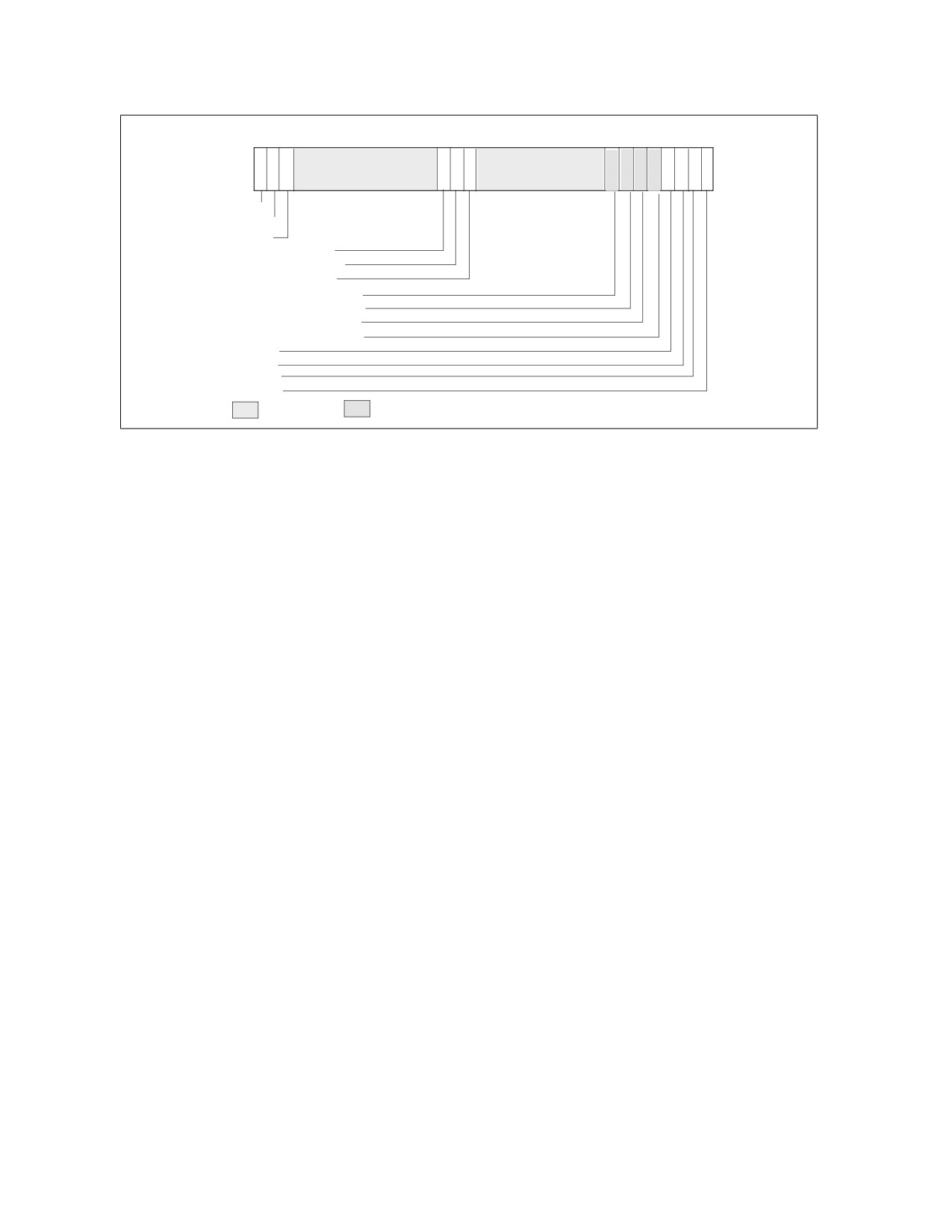
IA32_PERF_GLOBAL_OVF_CTL MSR allows software to clear overflow the indicators for general-purpose or fixed-
function counters via a single WRMSR (see Figure 20-28). Clear overflow indications when:
• Setting up new values in the event select and/or UMASK field for counting or interrupt based sampling.
• Reloading counter values to continue sampling.
• Disabling event counting or interrupt based sampling.
Vol. 3B
20-35
PERFORMANCE MONITORING
6362
3534333231
87
6 5
43
2 10
ClrCondChgd
ClrOvfDSBuffer
ClrOvfUncore
FIXED_CTR2 ClrOverflow
FIXED_CTR1 ClrOverflow
FIXED_CTR0 ClrOverflow
PMC7_ClrOvf (if PMC7 present)
PMC6_ClrOvf (if PMC6 present)
PMC5_ClrOvf (if PMC5 present)
PMC4_ClrOvf (if PMC4 present)
PMC3_ClrOvf
PMC2_ClrOvf
PMC1_ClrOvf
PMC0_ClrOvf
Reserved
Valid if CPUID.0AH:EAX[15:8] = 8; else reserved
Figure 20-28. IA32_PERF_GLOBAL_OVF_CTRL MSR in Sandy Bridge Microarchitecture
20.3.4.2 Counter Coalescence
In processors based on Sandy Bridge microarchitecture, each processor core implements eight general-purpose
counters. CPUID.0AH:EAX[15:8] will report the number of counters visible to software.
If a processor core is shared by two logical processors, each logical processors can access up to four counters
(IA32_PMC0-IA32_PMC3). This is the same as in the prior generation for processors based on Nehalem microarchi-
tecture.
If a processor core is not shared by two logical processors, up to eight general-purpose counters are visible. If
CPUID.0AH:EAX[15:8] reports 8 counters, then IA32_PMC4-IA32_PMC7 would occupy MSR addresses 0C5H
through 0C8H. Each counter is accompanied by an event select MSR (IA32_PERFEVTSEL4-IA32_PERFEVTSEL7).
If CPUID.0AH:EAX[15:8] report 4, access to IA32_PMC4-IA32_PMC7, IA32_PMC4-IA32_PMC7 will cause #GP.
Writing 1’s to bit position 7:4 of IA32_PERF_GLOBAL_CTRL, IA32_PERF_GLOBAL_STATUS, or IA32_PERF_-
GLOBAL_OVF_CTL will also cause #GP.
20.3.4.3 Full Width Writes to Performance Counters
Processors based on Sandy Bridge microarchitecture support full-width writes to the general-purpose counters,
IA32_PMCx. Support of full-width writes are enumerated by IA32_PERF_CAPABILITIES.FW_WRITES[13] (see
Section 20.2.4).
The default behavior of IA32_PMCx is unchanged, i.e., WRMSR to IA32_PMCx results in a sign-extended 32-bit
value of the input EAX written into IA32_PMCx. Full-width writes must issue WRMSR to a dedicated alias MSR
address for each IA32_PMCx.
Software must check the presence of full-width write capability and the presence of the alias address IA32_A_PMCx
by testing IA32_PERF_CAPABILITIES[13].
20.3.4.4 PEBS Support in Sandy Bridge Microarchitecture
Processors based on Sandy Bridge microarchitecture support PEBS, similar to those offered in prior generation,
with several enhanced features. The key components and differences of PEBS facility relative to Westmere microar-
chitecture is summarized in Table 20-11.
20-36
Vol. 3B

PERFORMANCE MONITORING
Table 20-11. PEBS Facility Comparison
Box
Sandy Bridge Microarchitecture
Westmere Microarchitecture
Comment
Valid IA32_PMCx
PMC0-PMC3
PMC0-PMC3
No PEBS on PMC4-PMC7.
PEBS Buffer Programming
Section 20.3.1.1.1
Section 20.3.1.1.1
Unchanged
IA32_PEBS_ENABLE
Figure 20-29
Figure 20-15
Layout
PEBS record layout
Physical Layout same as
Table 20-3
Enhanced fields at offsets
Table 20-3.
98H, A0H, A8H.
PEBS Events
See Table 20-12.
See Table 20-84.
IA32_PMC4-IA32_PMC7 do
not support PEBS.
PEBS-Load Latency
See Table 20-13.
Table 20-4
PEBS-Precise Store
Yes; see Section 20.3.4.4.3.
No
IA32_PMC3 only
PEBS-PDIR
Yes
No
IA32_PMC1 only
PEBS skid from EventingIP
1 (or 2 if micro+macro fusion)
1
SAMPLING Restriction
Small SAV(CountDown) value incur higher overhead than prior
generation.
Only IA32_PMC0 through IA32_PMC3 support PEBS.
NOTE
PEBS events are only valid when the following fields of IA32_PERFEVTSELx are all zero: AnyThread,
Edge, Invert, CMask.
In a PMU with PDIR capability, PEBS behavior is unpredictable if IA32_PERFEVTSELx or IA32_PMCx
is changed for a PEBS-enabled counter while an event is being counted. To avoid this, changes to
the programming or value of a PEBS-enabled counter should be performed when the counter is
disabled.
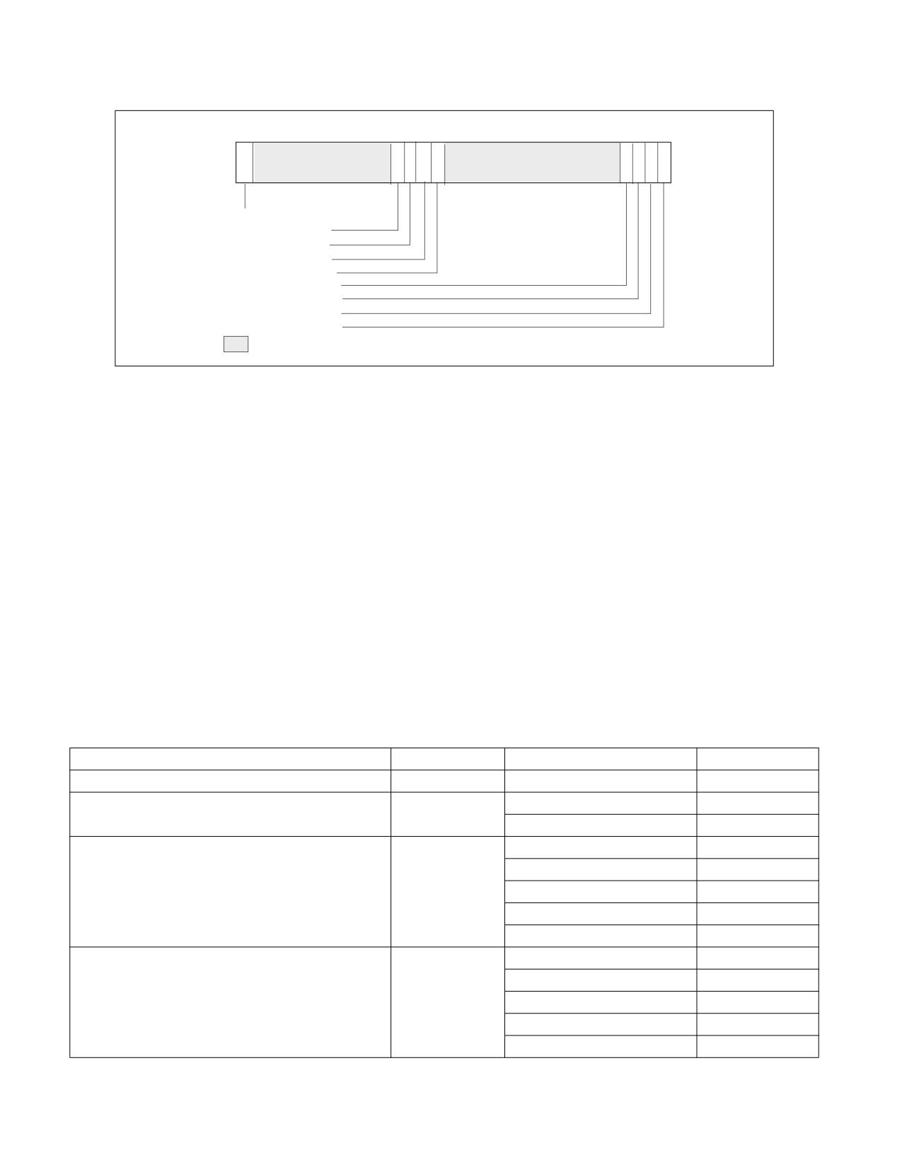
In IA32_PEBS_ENABLE MSR, bit 63 is defined as PS_ENABLE: When set, this enables IA32_PMC3 to capture
precise store information. Only IA32_PMC3 supports the precise store facility. In typical usage of PEBS, the bit
fields in IA32_PEBS_ENABLE are written to when the agent software starts PEBS operation; the enabled bit fields
should be modified only when re-programming another PEBS event or cleared when the agent uses the perfor-
mance counters for non-PEBS operations.
Vol. 3B
20-37
PERFORMANCE MONITORING
63
62
36 3534
33 32
31
8 7
6
5 4
3
2
1
0
PS_EN (R/W)
LL_EN_PMC3 (R/W)
LL_EN_PMC2 (R/W)
LL_EN_PMC1 (R/W)
LL_EN_PMC0 (R/W)
PEBS_EN_PMC3 (R/W)
PEBS_EN_PMC2 (R/W)
PEBS_EN_PMC1 (R/W)
PEBS_EN_PMC0 (R/W)
Reserved
RESET Value — 00000000_00000000H
Figure 20-29. Layout of IA32_PEBS_ENABLE MSR
20.3.4.4.1 PEBS Record Format
The layout of PEBS records physically identical to those shown in Table 20-3, but the fields at offsets 98H, A0H, and
A8H have been enhanced to support additional PEBS capabilities.
• Load/Store Data Linear Address (Offset 98H): This field will contain the linear address of the source of the load,
or linear address of the destination of the store.
• Data Source /Store Status (Offset A0H): When load latency is enabled, this field will contain three piece of
information (including an encoded value indicating the source which satisfied the load operation). The source
field encodings are detailed in Table 20-4. When precise store is enabled, this field will contain information
indicating the status of the store, as detailed in Table 19.
• Latency Value/0 (Offset A8H): When load latency is enabled, this field contains the latency in cycles to service
the load. This field is not meaningful when precise store is enabled and will be written to zero in that case. Upon
writing the PEBS record, microcode clears the overflow status bits in the IA32_PERF_GLOBAL_STATUS corre-
sponding to those counters that both overflowed and were enabled in the IA32_PEBS_ENABLE register. The
status bits of other counters remain unaffected.
The number PEBS events has expanded. The list of PEBS events supported in Sandy Bridge microarchitecture is
shown in Table 20-12.
Table 20-12. PEBS Performance Events for Sandy Bridge Microarchitecture
Event Name
Event Select
Sub-event
UMask
INST_RETIRED
C0H
PREC_DIST
01H1
UOPS_RETIRED
C2H
All
01H
Retire_Slots
02H
BR_INST_RETIRED
C4H
Conditional
01H
Near_Call
02H
All_branches
04H
Near_Return
08H
Near_Taken
20H
BR_MISP_RETIRED
C5H
Conditional
01H
Near_Call
02H
All_branches
04H
Not_Taken
10H
Taken
20H
20-38
Vol. 3B

PERFORMANCE MONITORING
Table 20-12. PEBS Performance Events for Sandy Bridge Microarchitecture (Contd.)
Event Name
Event Select
Sub-event
UMask
MEM_UOPS_RETIRED
D0H
STLB_MISS_LOADS
11H
STLB_MISS_STORE
12H
LOCK_LOADS
21H
SPLIT_LOADS
41H
SPLIT_STORES
42H
ALL_LOADS
81H
ALL_STORES
82H
MEM_LOAD_UOPS_RETIRED
D1H
L1_Hit
01H
L2_Hit
02H
L3_Hit
04H
Hit_LFB
40H
MEM_LOAD_UOPS_LLC_HIT_RETIRED
D2H
XSNP_Miss
01H
XSNP_Hit
02H
XSNP_Hitm
04H
XSNP_None
08H
NOTES:
1. Only available on IA32_PMC1.
20.3.4.4.2 Load Latency Performance Monitoring Facility
The load latency facility in Sandy Bridge microarchitecture is similar to that in prior microarchitectures. It provides
software a means to characterize the average load latency to different levels of cache/memory hierarchy. This
facility requires processor supporting enhanced PEBS record format in the PEBS buffer, see Table 20-3 and Section
20.3.4.4.1. This field measures the load latency from load's first dispatch of till final data writeback from the
memory subsystem. The latency is reported for retired demand load operations and in core cycles (it accounts for
re-dispatches).
To use this feature software must assure:
• One of the IA32_PERFEVTSELx MSR is programmed to specify the event unit MEM_TRANS_RETIRED, and the
LATENCY_ABOVE_THRESHOLD event mask must be specified (IA32_PerfEvtSelX[15:0] = 1CDH). The corre-
sponding counter IA32_PMCx will accumulate event counts for architecturally visible loads which exceed the
programmed latency threshold specified separately in a MSR. Stores are ignored when this event is
programmed. The CMASK or INV fields of the IA32_PerfEvtSelX register used for counting load latency must be
0. Writing other values will result in undefined behavior.
• The MSR_PEBS_LD_LAT_THRESHOLD MSR is programmed with the desired latency threshold in core clock
cycles. Loads with latencies greater than this value are eligible for counting and latency data reporting. The
minimum value that may be programmed in this register is 3 (the minimum detectable load latency is 4 core
clock cycles).
• The PEBS enable bit in the IA32_PEBS_ENABLE register is set for the corresponding IA32_PMCx counter
register. This means that both the PEBS_EN_CTRX and LL_EN_CTRX bits must be set for the counter(s) of
interest. For example, to enable load latency on counter IA32_PMC0, the IA32_PEBS_ENABLE register must be
programmed with the 64-bit value 00000001.00000001H.
• When Load latency event is enabled, no other PEBS event can be configured with other counters.
When the load-latency facility is enabled, load operations are randomly selected by hardware and tagged to carry
information related to data source locality and latency. Latency and data source information of tagged loads are
updated internally. The MEM_TRANS_RETIRED event for load latency counts only tagged retired loads. If a load is
cancelled it will not be counted and the internal state of the load latency facility will not be updated. In this case the
hardware will tag the next available load.
Vol. 3B
20-39

PERFORMANCE MONITORING
When a PEBS assist occurs, the last update of latency and data source information are captured by the assist and
written as part of the PEBS record. The PEBS sample after value (SAV), specified in PEBS CounterX Reset, operates
orthogonally to the tagging mechanism. Loads are randomly tagged to collect latency data. The SAV controls the
number of tagged loads with latency information that will be written into the PEBS record field by the PEBS assists.
The load latency data written to the PEBS record will be for the last tagged load operation which retired just before
the PEBS assist was invoked.
The physical layout of the PEBS records is the same as shown in Table 20-3. The specificity of Data Source entry at
offset A0H has been enhanced to report three pieces of information.
Table 20-13. Layout of Data Source Field of Load Latency Record
Field
Position
Description
Source
3:0
See Table 20-4
STLB_MISS
4
0: The load did not miss the STLB (hit the DTLB or STLB).
1: The load missed the STLB.
Lock
5
0: The load was not part of a locked transaction.
1: The load was part of a locked transaction.
Reserved
63:6
Reserved
The layout of MSR_PEBS_LD_LAT_THRESHOLD is the same as shown in Figure 20-17.
20.3.4.4.3 Precise Store Facility
Processors based on Sandy Bridge microarchitecture offer a precise store capability that complements the load
latency facility. It provides a means to profile store memory references in the system.
Precise stores leverage the PEBS facility and provide additional information about sampled stores. Having precise
memory reference events with linear address information for both loads and stores can help programmers improve
data structure layout, eliminate remote node references, and identify cache-line conflicts in NUMA systems.
Only IA32_PMC3 can be used to capture precise store information. After enabling this facility, counter overflows will
initiate the generation of PEBS records as previously described in PEBS. Upon counter overflow hardware captures
the linear address and other status information of the next store that retires. This information is then written to the
PEBS record.
To enable the precise store facility, software must complete the following steps. Please note that the precise store
facility relies on the PEBS facility, so the PEBS configuration requirements must be completed before attempting to
capture precise store information.
• Complete the PEBS configuration steps.
• Program the MEM_TRANS_RETIRED.PRECISE_STORE event in IA32_PERFEVTSEL3. Only counter 3
(IA32_PMC3) supports collection of precise store information.
• Set IA32_PEBS_ENABLE[3] and IA32_PEBS_ENABLE[63]. This enables IA32_PMC3 as a PEBS counter and
enables the precise store facility, respectively.
The precise store information written into a PEBS record affects entries at offsets 98H, A0H, and A8H of Table 20-3.
The specificity of Data Source entry at offset A0H has been enhanced to report three piece of information.
20-40
Vol. 3B

PERFORMANCE MONITORING
Table 20-14. Layout of Precise Store Information In PEBS Record
Field
Offset
Description
Store Data
98H
The linear address of the destination of the store.
Linear Address
Store Status
A0H
L1D Hit (Bit 0): The store hit the data cache closest to the core (lowest latency cache) if this bit is set,
otherwise the store missed the data cache.
STLB Miss (bit 4): The store missed the STLB if set, otherwise the store hit the STLB
Locked Access (bit 5): The store was part of a locked access if set, otherwise the store was not part of a
locked access.
Reserved
A8H
Reserved
20.3.4.4.4 Precise Distribution of Instructions Retired (PDIR)
Upon triggering a PEBS assist, there will be a finite delay between the time the counter overflows and when the
microcode starts to carry out its data collection obligations. INST_RETIRED is a very common event that is used to
sample where performance bottleneck happened and to help identify its location in instruction address space. Even
if the delay is constant in core clock space, it invariably manifest as variable “skids” in instruction address space.
This creates a challenge for programmers to profile a workload and pinpoint the location of bottlenecks.
The core PMU in processors based on Sandy Bridge microarchitecture include a facility referred to as precise distri-
bution of Instruction Retired (PDIR).
The PDIR facility mitigates the “skid” problem by providing an early indication of when the INST_RETIRED counter
is about to overflow, allowing the machine to more precisely trap on the instruction that actually caused the
counter overflow. On processors based on Sandy Bridge microarchitecture, skid is significantly reduced and can be
as little as one instruction. On future implementations, PDIR may eliminate skid.
PDIR applies only to the INST_RETIRED.ALL precise event, and processors based on Sandy Bridge microarchitec-
ture must use IA32_PMC1 with PerfEvtSel1 property configured and bit 1 in the IA32_PEBS_ENABLE set to 1.
INST_RETIRED.ALL is a non-architectural performance event, it is not supported in prior generation microarchitec-
tures. Additionally, on processors with CPUID DisplayFamily_DisplayModel signatures of 06_2A and 06_2D, the tool
that programs PDIR should quiesce the rest of the programmable counters in the core when PDIR is active.
20.3.4.5 Off-core Response Performance Monitoring
The core PMU in processors based on Sandy Bridge microarchitecture provides off-core response facility similar to
prior generation. Off-core response can be programmed only with a specific pair of event select and counter MSR,
and with specific event codes and predefine mask bit value in a dedicated MSR to specify attributes of the off-core
transaction. Two event codes are dedicated for off-core response event programming. Each event code for off-core
response monitoring requires programming an associated configuration MSR, MSR_OFFCORE_RSP_x. Table 20-15
lists the event code, mask value and additional off-core configuration MSR that must be programmed to count off-
core response events using IA32_PMCx.
Table 20-15. Off-Core Response Event Encoding
Counter
Event code
UMask
Required Off-core Response MSR
PMC0-3
B7H
01H
MSR_OFFCORE_RSP_0 (address 1A6H)
PMC0-3
BBH
01H
MSR_OFFCORE_RSP_1 (address 1A7H)
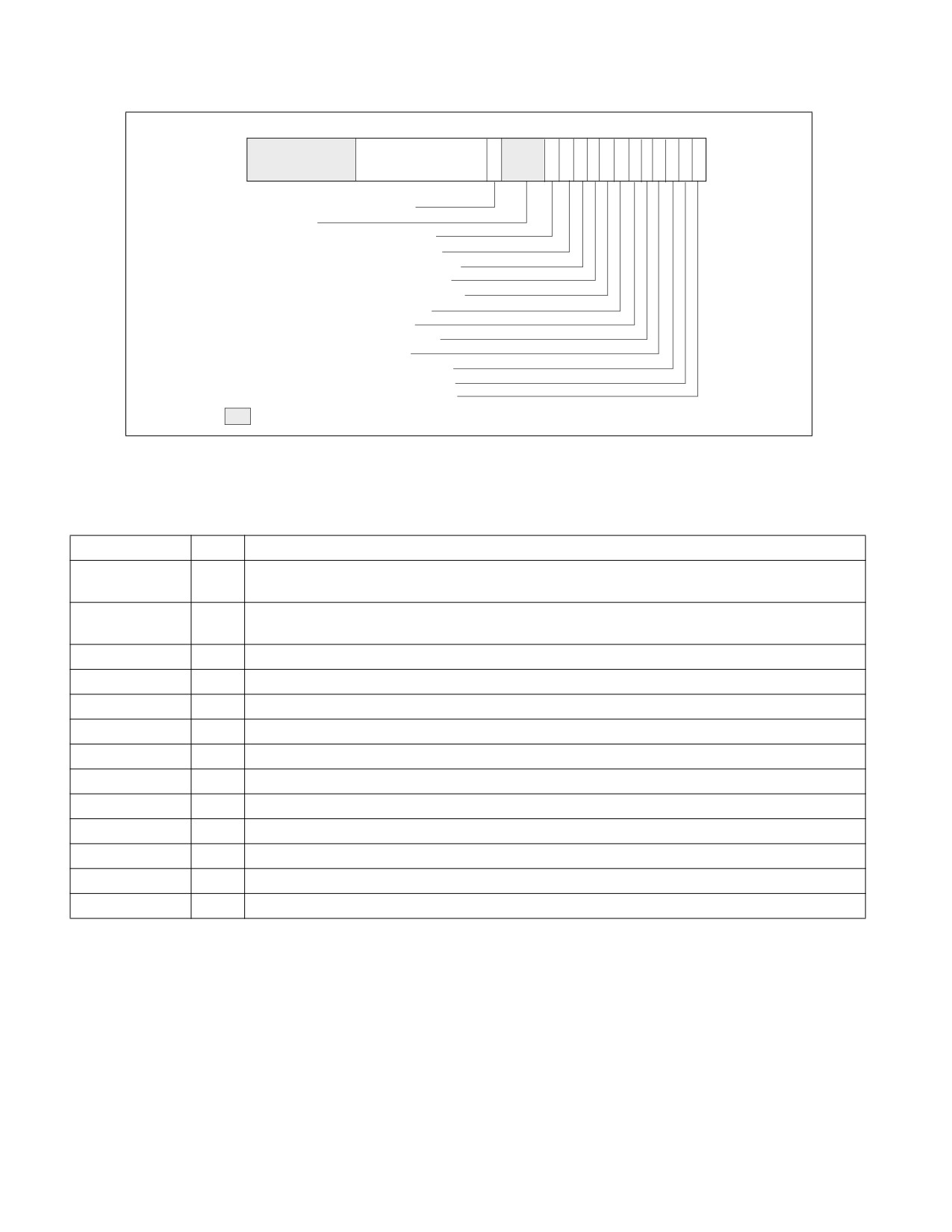
The layout of MSR_OFFCORE_RSP_0 and MSR_OFFCORE_RSP_1 are shown in Figure 20-30 and Figure 20-31. Bits
15:0 specifies the request type of a transaction request to the uncore. Bits 30:16 specifies supplier information,
bits 37:31 specifies snoop response information.
Vol. 3B
20-41
PERFORMANCE MONITORING
63
37
15 14 1312 11
10
9
8 7
6
5
4
3
2
1
0
See Figure 18-30
RESPONSE TYPE — Other (R/W)
RESERVED
REQUEST TYPE — STRM_ST (R/W)
REQUEST TYPE — BUS_LOCKS (R/W)
REQUEST TYPE — PF_LLC_IFETCH (R/W)
REQUEST TYPE — PF_LLC_RFO (R/W)
REQUEST TYPE — PF_LLC_DATA_RD (R/W)
REQUEST TYPE — PF_IFETCH (R/W)
REQUEST TYPE — PF_RFO (R/W)
REQUEST TYPE — PF_DATA_RD (R/W)
REQUEST TYPE — WB (R/W)
REQUEST TYPE — DMND_IFETCH (R/W)
REQUEST TYPE — DMND_RFO (R/W)
REQUEST TYPE — DMND_DATA_RD (R/W)
Reserved
RESET Value — 00000000_00000000H
Figure 20-30. Request_Type Fields for MSR_OFFCORE_RSP_x
Table 20-16. MSR_OFFCORE_RSP_x Request_Type Field Definition
Bit Name
Offset
Description
DMND_DATA_RD
0
Counts the number of demand data reads of full and partial cachelines as well as demand data page
table entry cacheline reads. Does not count L2 data read prefetches or instruction fetches.
DMND_RFO
1
Counts the number of demand and DCU prefetch reads for ownership (RFO) requests generated by a
write to data cacheline. Does not count L2 RFO prefetches.
DMND_IFETCH
2
Counts the number of demand instruction cacheline reads and L1 instruction cacheline prefetches.
WB
3
Counts the number of writeback (modified to exclusive) transactions.
PF_DATA_RD
4
Counts the number of data cacheline reads generated by L2 prefetchers.
PF_RFO
5
Counts the number of RFO requests generated by L2 prefetchers.
PF_IFETCH
6
Counts the number of code reads generated by L2 prefetchers.
PF_LLC_DATA_RD
7
L2 prefetcher to L3 for loads.
PF_LLC_RFO
8
RFO requests generated by L2 prefetcher
PF_LLC_IFETCH
9
L2 prefetcher to L3 for instruction fetches.
BUS_LOCKS
10
Bus lock and split lock requests
STRM_ST
11
Streaming store requests
OTHER
15
Any other request that crosses IDI, including I/O.
20-42
Vol. 3B
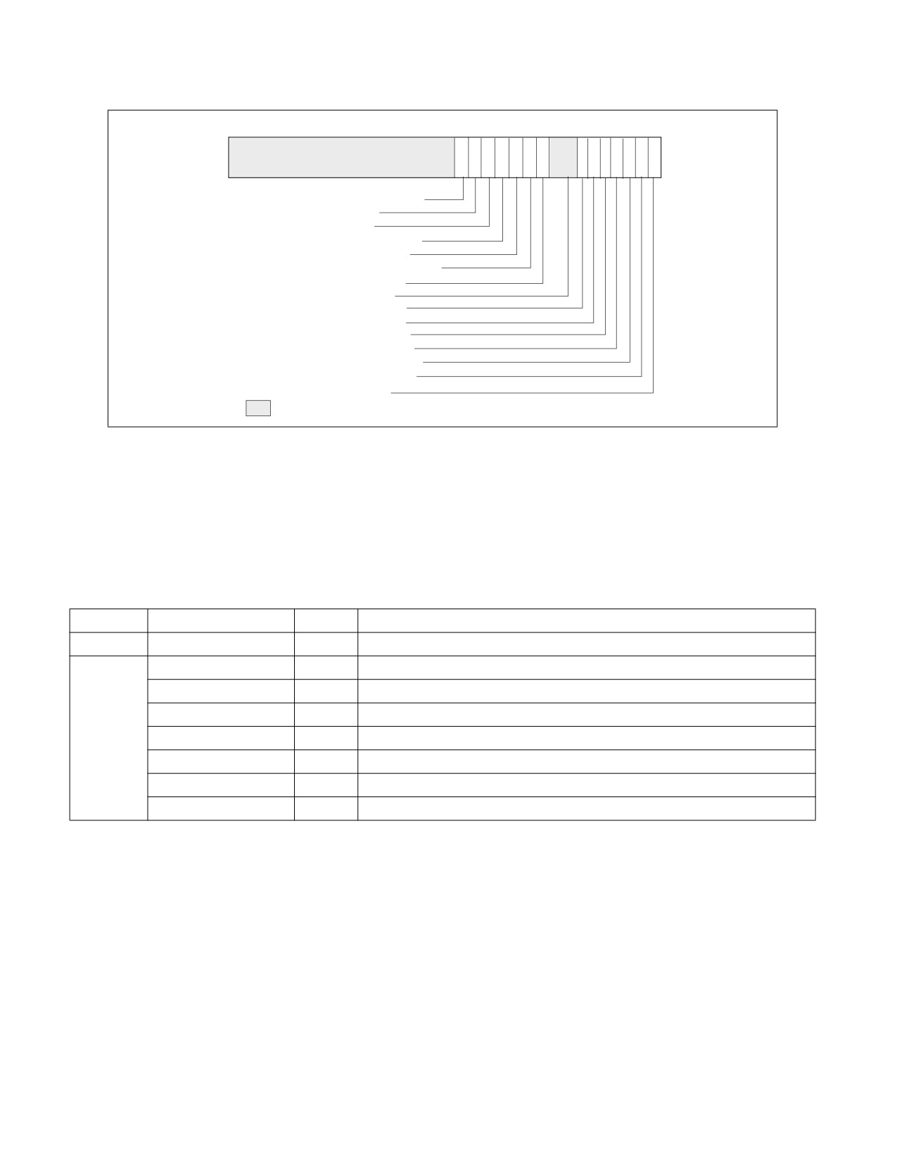
PERFORMANCE MONITORING
63
37 36 35
34 33
32
31
22 2120
19
18
17 16
RESPONSE TYPE — NON_DRAM (R/W)
RSPNS_SNOOP — HITM (R/W)
RSPNS_SNOOP — HIT_FWD
RSPNS_SNOOP — HIT_NO_FWD (R/W)
RSPNS_SNOOP — SNP_MISS (R/W)
RSPNS_SNOOP — SNP_NOT_NEEDED (R/W)
RSPNS_SNOOP — SNPl_NONE (R/W)
RSPNS_SUPPLIER — RESERVED
RSPNS_SUPPLIER — Local
RSPNS_SUPPLIER — LLC_HITF (R/W)
RSPNS_SUPPLIER — LLC_HITS (R/W)
RSPNS_SUPPLIER — LLC_HITE (R/W)
RSPNS_SUPPLIER — LLC_HITM (R/W)
RSPNS_SUPPLIER — No_SUPP (R/W)
RSPNS_SUPPLIER — ANY (R/W)
Reserved
RESET Value — 00000000_00000000H
Figure 20-31. Response_Supplier and Snoop Info Fields for MSR_OFFCORE_RSP_x
To properly program this extra register, software must set at least one request type bit and a valid response type
pattern. Otherwise, the event count reported will be zero. It is permissible and useful to set multiple request and
response type bits in order to obtain various classes of off-core response events. Although MSR_OFFCORE_RSP_x
allow an agent software to program numerous combinations that meet the above guideline, not all combinations
produce meaningful data.
Table 20-17. MSR_OFFCORE_RSP_x Response Supplier Info Field Definition
Subtype
Bit Name
Offset
Description
Common
Any
16
Catch all value for any response types.
Supplier
NO_SUPP
17
No Supplier Information available.
Info
LLC_HITM
18
M-state initial lookup stat in L3.
LLC_HITE
19
E-state
LLC_HITS
20
S-state
LLC_HITF
21
F-state
LOCAL
22
Local DRAM Controller.
Reserved
30:23
Reserved
To specify a complete offcore response filter, software must properly program bits in the request and response type
fields. A valid request type must have at least one bit set in the non-reserved bits of 15:0. A valid response type
must be a non-zero value of the following expression:
ANY | [(‘OR’ of Supplier Info Bits) & (‘OR’ of Snoop Info Bits)]
If “ANY“ bit is set, the supplier and snoop info bits are ignored.
Vol. 3B
20-43
PERFORMANCE MONITORING
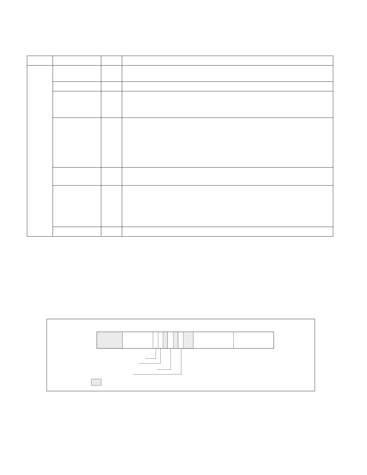
Table 20-18. MSR_OFFCORE_RSP_x Snoop Info Field Definition
Subtype
Bit Name
Offset
Description
Snoop
SNP_NONE
31
No details on snoop-related information.
Info
SNP_NOT_NEEDED
32
No snoop was needed to satisfy the request.
SNP_MISS
33
A snoop was needed and it missed all snooped caches:
-For LLC Hit, ReslHitl was returned by all cores
-For LLC Miss, Rspl was returned by all sockets and data was returned from DRAM.
SNP_NO_FWD
34
A snoop was needed and it hits in at least one snooped cache. Hit denotes a cache-line was
valid before snoop effect. This includes:
-Snoop Hit w/ Invalidation (LLC Hit, RFO)
-Snoop Hit, Left Shared (LLC Hit/Miss, IFetch/Data_RD)
-Snoop Hit w/ Invalidation and No Forward (LLC Miss, RFO Hit S)
In the LLC Miss case, data is returned from DRAM.
SNP_FWD
35
A snoop was needed and data was forwarded from a remote socket. This includes:
-Snoop Forward Clean, Left Shared (LLC Hit/Miss, IFetch/Data_RD/RFT).
HITM
36
A snoop was needed and it HitM-ed in local or remote cache. HitM denotes a cache-line was
in modified state before effect as a results of snoop. This includes:
-Snoop HitM w/ WB (LLC miss, IFetch/Data_RD)
-Snoop Forward Modified w/ Invalidation (LLC Hit/Miss, RFO)
-Snoop MtoS (LLC Hit, IFetch/Data_RD).
NON_DRAM
37
Target was non-DRAM system address. This includes MMIO transactions.
20.3.4.6 Uncore Performance Monitoring Facilities in the Intel® Core™ i7-2xxx, Intel® Core™ i5-2xxx,
and Intel® Core™ i3-2xxx Processor Series
The uncore sub-system in Intel® Core™ i7-2xxx, Intel® Core™ i5-2xxx, Intel® Core™ i3-2xxx processor series
provides a unified L3 that can support up to four processor cores. The L3 cache consists multiple slices, each slice
interface with a processor via a coherence engine, referred to as a C-Box. Each C-Box provides dedicated facility of
MSRs to select uncore performance monitoring events and each C-Box event select MSR is paired with a counter
register, similar in style as those described in Section 20.3.1.2.2. The ARB unit in the uncore also provides its local
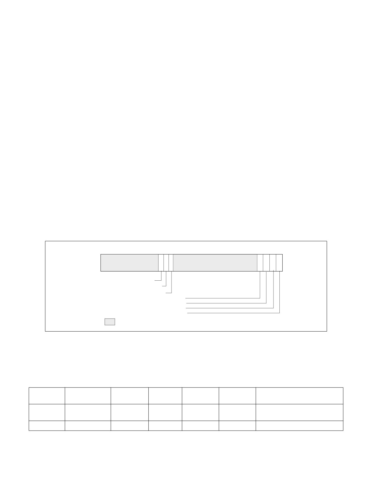
performance counters and event select MSRs. The layout of the event select MSRs in the C-Boxes and the ARB unit
are shown in Figure 20-32.
63
28
2423222120191817 16 15
8 7
0
Counter Mask
Unit Mask (UMASK)
Event Select
(CMASK)
INV—Invert counter mask
EN—Enable counter
OVF_EN—Overflow forwarding
E—Edge detect
Reserved
RESET Value — 00000000_00000000H
Figure 20-32. Layout of Uncore PERFEVTSEL MSR for a C-Box Unit or the ARB Unit
20-44
Vol. 3B
PERFORMANCE MONITORING
The bit fields of the uncore event select MSRs for a C-box unit or the ARB unit are summarized below:
• Event_Select (bits 7:0) and UMASK (bits 15:8): Specifies the microarchitectural condition to count in a local
uncore PMU counter, see the event list at: https://perfmon-events.intel.com/.
• E (bit 18): Enables edge detection filtering, if 1.
• OVF_EN (bit 20): Enables the overflow indicator from the uncore counter forwarded to MSR_UNC_PERF_-
GLOBAL_CTRL, if 1.
• EN (bit 22): Enables the local counter associated with this event select MSR.
• INV (bit 23): Event count increments with non-negative value if 0, with negated value if 1.
• CMASK (bits 28:24): Specifies a positive threshold value to filter raw event count input.
At the uncore domain level, there is a master set of control MSRs that centrally manages all the performance moni-
toring facility of uncore units. Figure 20-33 shows the layout of the uncore domain global control.
When an uncore counter overflows, a PMI can be routed to a processor core. Bits 3:0 of MSR_UNC_PERF_-
GLOBAL_CTRL can be used to select which processor core to handle the uncore PMI. Software must then write to
bit 13 of IA32_DEBUGCTL (at address 1D9H) to enable this capability.
• PMI_SEL_Core#: Enables the forwarding of an uncore PMI request to a processor core, if 1. If bit 30 (WakePMI)
is ‘1’, a wake request is sent to the respective processor core prior to sending the PMI.
• EN: Enables the fixed uncore counter, the ARB counters, and the CBO counters in the uncore PMU, if 1. This bit
is cleared if bit 31 (FREEZE) is set and any enabled uncore counters overflow.
• WakePMI: Controls sending a wake request to any halted processor core before issuing the uncore PMI request.
If a processor core was halted and not sent a wake request, the uncore PMI will not be serviced by the
processor core.
• FREEZE: Provides the capability to freeze all uncore counters when an overflow condition occurs in a unit
counter. When this bit is set, and a counter overflow occurs, the uncore PMU logic will clear the global enable
bit (bit 29).
63
32313029
28
4 3
2
1
0
FREEZE—Freeze counters
WakePMI—Wake cores on PMI
EN—Enable all uncore counters
PMI_Sel_Core3 — Uncore PMI to core 3
PMI_Sel_Core2 — Uncore PMI to core 2
PMI_Sel_Core1 — Uncore PMI to core 1
PMI_Sel_Core0 — Uncore PMI to core 0
Reserved
RESET Value — 00000000_00000000H
Figure 20-33. Layout of MSR_UNC_PERF_GLOBAL_CTRL MSR for Uncore
Additionally, there is also a fixed counter, counting uncore clockticks, for the uncore domain. Table 20-19 summa-
rizes the number MSRs for uncore PMU for each box.
Table 20-19. Uncore PMU MSR Summary
Counters per
Counter
General
Global
Box
# of Boxes
Box
Width
Purpose
Enable
Comment
C-Box
SKU specific
2
44
Yes
Per-box
Up to 4, seeTable 2-21
MSR_UNC_CBO_CONFIG
ARB
1
2
44
Yes
Uncore
Vol. 3B
20-45

PERFORMANCE MONITORING
Table 20-19. Uncore PMU MSR Summary (Contd.)
Counters per
Counter
General
Global
Box
# of Boxes
Box
Width
Purpose
Enable
Comment
Fixed
N.A.
N.A.
48
No
Uncore
Counter
20.3.4.6.1 Uncore Performance Monitoring Events
There are certain restrictions on the uncore performance counters in each C-Box. Specifically,
• Occupancy events are supported only with counter 0 but not counter 1.
• Other uncore C-Box events can be programmed with either counter 0 or 1.
The C-Box uncore performance events can collect performance characteristics of transactions initiated by
processor core. In that respect, they are similar to various sub-events in the OFFCORE_RESPONSE family of perfor-
mance events in the core PMU. Information such as data supplier locality (LLC HIT/MISS) and snoop responses can
be collected via OFFCORE_RESPONSE and qualified on a per-thread basis.
On the other hand, uncore performance event logic cannot associate its counts with the same level of per-thread
qualification attributes as the core PMU events can. Therefore, whenever similar event programming capabilities
are available from both core PMU and uncore PMU, the recommendation is that utilizing the core PMU events may
be less affected by artifacts, complex interactions and other factors.
20.3.4.7 Intel® Xeon® Processor E5 Family Performance Monitoring Facility
The Intel® Xeon® Processor E5 Family (and Intel® Core™ i7-3930K Processor) are based on Sandy Bridge-E
microarchitecture. While the processor cores share the same microarchitecture as those of the Intel® Xeon®
Processor E3 Family and 2nd generation Intel Core i7-2xxx, Intel Core i5-2xxx, Intel Core i3-2xxx processor series,
the uncore subsystems are different. An overview of the uncore performance monitoring facilities of the Intel Xeon
processor E5 family (and Intel Core i7-3930K processor) is described in Section 20.3.4.8.
Thus, the performance monitoring facilities in the processor core generally are the same as those described in
Section 20.6.3 through Section 20.3.4.5. However, the MSR_OFFCORE_RSP_0/MSR_OFFCORE_RSP_1 Response
Supplier Info field shown in Table 20-17 applies to Intel Core Processors with CPUID signature of DisplayFami-
ly_DisplayModel encoding of 06_2AH; Intel Xeon processor with CPUID signature of DisplayFamily_DisplayModel
encoding of 06_2DH supports an additional field for remote DRAM controller shown in Table 20-20. Additionally,
there are some small differences in the non-architectural performance monitoring events (see event list available
Table 20-20. MSR_OFFCORE_RSP_x Supplier Info Field Definitions
Subtype
Bit Name
Offset
Description
Common
Any
16
Catch all value for any response types.
Supplier Info
NO_SUPP
17
No Supplier Information available.
LLC_HITM
18
M-state initial lookup stat in L3.
LLC_HITE
19
E-state
LLC_HITS
20
S-state
LLC_HITF
21
F-state
LOCAL
22
Local DRAM Controller.
Remote
30:23
Remote DRAM Controller (either all 0s or all 1s).
20-46
Vol. 3B

PERFORMANCE MONITORING
20.3.4.8 Intel® Xeon® Processor E5 Family Uncore Performance Monitoring Facility
The uncore subsystem in the Intel Xeon processor E5-2600 product family has some similarities with those of the
Intel Xeon processor E7 family. Within the uncore subsystem, localized performance counter sets are provided at
logic control unit scope. For example, each Cbox caching agent has a set of local performance counters, and the
power controller unit (PCU) has its own local performance counters. Up to 8 C-Box units are supported in the
uncore sub-system.
Table 20-21 summarizes the uncore PMU facilities providing MSR interfaces.
Table 20-21. Uncore PMU MSR Summary for Intel® Xeon® Processor E5 Family
Counter
General
Global
Box
# of Boxes
Counters per Box
Width
Purpose
Enable
Sub-control MSRs
C-Box
8
4
44
Yes
per-box
None
PCU
1
4
48
Yes
per-box
Match/Mask
U-Box
1
2
44
Yes
uncore
None
Details of the uncore performance monitoring facility of Intel Xeon Processor E5 family is available in “Intel®
Xeon® Processor E5 Uncore Performance Monitoring Programming Reference Manual”. The MSR-based uncore
PMU interfaces are listed in Table 2-24.
20.3.5
3rd Generation Intel® Core™ Processor Performance Monitoring Facility
The 3rd generation Intel® Core™ processor family and Intel® Xeon® processor E3-1200v2 product family are
based on the Ivy Bridge microarchitecture. The performance monitoring facilities in the processor core generally
are the same as those described in Section 20.6.3 through Section 20.3.4.5. The non-architectural performance
monitoring events supported by the processor core can be found at: https://perfmon-events.intel.com/.
20.3.5.1 Intel® Xeon® Processor E5 v2 and E7 v2 Family Uncore Performance Monitoring Facility
The uncore subsystem in the Intel Xeon processor E5 v2 and Intel Xeon Processor E7 v2 product families are based
on the Ivy Bridge-E microarchitecture. There are some similarities with those of the Intel Xeon processor E5 family
based on the Sandy Bridge microarchitecture. Within the uncore subsystem, localized performance counter sets
are provided at logic control unit scope.
Details of the uncore performance monitoring facility of Intel Xeon Processor E5 v2 and Intel Xeon Processor E7 v2
families are available in the “Intel® Xeon® Processor E5 v2 and E7 v2 Uncore Performance Monitoring Program-
ming Reference Manual”. The MSR-based uncore PMU interfaces are listed in Table 2-28.
20.3.6
4th Generation Intel® Core™ Processor Performance Monitoring Facility
The 4th generation Intel® Core™ processor and Intel® Xeon® processor E3-1200 v3 product family are based on
the Haswell microarchitecture. The core PMU supports architectural performance monitoring capability with version
ID 3 (see Section 20.2.3) and a host of non-architectural monitoring capabilities.
Architectural performance monitoring version 3 capabilities are described in Section 20.2.3.
The core PMU’s capability is similar to those described in Section 20.6.3 through Section 20.3.4.5, with some differ-
ences and enhancements summarized in Table 20-22. Additionally, the core PMU provides some enhancement to
support performance monitoring when the target workload contains instruction streams using Intel® Transactional
Synchronization Extensions (TSX), see Section 20.3.6.5. For details of Intel TSX, see Chapter 16, “Programming with
Intel® Transactional Synchronization Extensions‚” of Intel® 64 and IA-32 Architectures Software Developer’s
Manual, Volume 1.
Vol. 3B
20-47

PERFORMANCE MONITORING
Table 20-22. Core PMU Comparison
Box
Haswell Microarchitecture
Sandy Bridge Microarchitecture
Comment
# of Fixed counters per thread
3
3
Use CPUID to determine #
of counters. See Section
20.2.1.
# of general-purpose counters
8
8
Use CPUID to determine #
per core
of counters. See Section
20.2.1.
Counter width (R,W)
R:48, W: 32/48
R:48, W: 32/48
See Section 20.2.2.
# of programmable counters
4 or (8 if a core not shared by two
4 or (8 if a core not shared by two
Use CPUID to determine #
per thread
threads)
threads)
of counters. See Section
20.2.1.
PMI Overhead Mitigation
• Freeze_Perfmon_on_PMI with
• Freeze_Perfmon_on_PMI with
See Section 18.4.7.
legacy semantics.
legacy semantics.
• Freeze_LBR_on_PMI with
• Freeze_LBR_on_PMI with
legacy semantics for branch
legacy semantics for branch
profiling.
profiling.
• Freeze_while_SMM.
• Freeze_while_SMM.
Processor Event Based
See Table 20-12 and Section
See Table 20-12.
IA32_PMC4-IA32_PMC7
Sampling (PEBS) Events
20.3.6.5.1.
do not support PEBS.
PEBS-Load Latency
See Section 20.3.4.4.2.
See Section 20.3.4.4.2.
PEBS-Precise Store
No, replaced by Data Address
Section 20.3.4.4.3
profiling.
PEBS-PDIR
Yes (using precise
Yes (using precise
INST_RETIRED.ALL)
INST_RETIRED.ALL)
PEBS-EventingIP
Yes
No
Data Address Profiling
Yes
No
LBR Profiling
Yes
Yes
Call Stack Profiling
Yes, see Section 18.11.
No
Use LBR facility.
Off-core Response Event
MSR 1A6H and 1A7H; extended
MSR 1A6H and 1A7H; extended
request and response types.
request and response types.
Intel TSX support for Perfmon
See Section 20.3.6.5.
No
20.3.6.1 Processor Event Based Sampling (PEBS) Facility
The PEBS facility in the 4th Generation Intel Core processor is similar to those in processors based on Sandy Bridge
microarchitecture, with several enhanced features. The key components and differences of PEBS facility relative to
Sandy Bridge microarchitecture is summarized in Table 20-23.
Table 20-23. PEBS Facility Comparison
Box
Haswell Microarchitecture
Sandy Bridge Microarchitecture
Comment
Valid IA32_PMCx
PMC0-PMC3
PMC0-PMC3
No PEBS on PMC4-PMC7
PEBS Buffer Programming
Section 20.3.1.1.1
Section 20.3.1.1.1
Unchanged
IA32_PEBS_ENABLE Layout
Figure 20-15
Figure 20-29
PEBS record layout
Table 20-24; enhanced fields
Table 20-3; enhanced fields at
at offsets 98H, A0H, A8H, B0H.
offsets 98H, A0H, A8H.
20-48
Vol. 3B

PERFORMANCE MONITORING
Table 20-23. PEBS Facility Comparison
Box
Haswell Microarchitecture
Sandy Bridge Microarchitecture
Comment
Precise Events
See Table 20-12.
See Table 20-12.
IA32_PMC4-IA32_PMC7 do
not support PEBS.
PEBS-Load Latency
See Table 20-13.
Table 20-13
PEBS-Precise Store
No, replaced by data address
Yes; see Section 20.3.4.4.3.
profiling.
PEBS-PDIR
Yes
Yes
IA32_PMC1 only.
PEBS skid from EventingIP
1 (or 2 if micro+macro fusion)
1
SAMPLING Restriction
Small SAV(CountDown) value incur higher overhead than prior
generation.
Only IA32_PMC0 through IA32_PMC3 support PEBS.
NOTE
PEBS events are only valid when the following fields of IA32_PERFEVTSELx are all zero: AnyThread,
Edge, Invert, CMask.
In a PMU with PDIR capability, PEBS behavior is unpredictable if IA32_PERFEVTSELx or IA32_PMCx
is changed for a PEBS-enabled counter while an event is being counted. To avoid this, changes to
the programming or value of a PEBS-enabled counter should be performed when the counter is
disabled.
20.3.6.2 PEBS Data Format
The PEBS record format for the 4th Generation Intel Core processor is shown in Table 20-24. The PEBS record
format, along with debug/store area storage format, does not change regardless of whether IA-32e mode is active
or not. CPUID.01H:ECX.DTES64[bit 2] reports whether the processor's DS storage format support is mode-inde-
pendent. When set, it uses 64-bit DS storage format.
Table 20-24. PEBS Record Format for 4th Generation Intel Core Processor Family
Byte Offset
Field
Byte Offset
Field
00H
R/EFLAGS
60H
R10
08H
R/EIP
68H
R11
10H
R/EAX
70H
R12
18H
R/EBX
78H
R13
20H
R/ECX
80H
R14
28H
R/EDX
88H
R15
30H
R/ESI
90H
IA32_PERF_GLOBAL_STATUS
38H
R/EDI
98H
Data Linear Address
40H
R/EBP
A0H
Data Source Encoding
48H
R/ESP
A8H
Latency value (core cycles)
50H
R8
B0H
EventingIP
58H
R9
B8H
TX Abort Information (Section
20.3.6.5.1)
Vol. 3B
20-49

PERFORMANCE MONITORING
The layout of PEBS records are almost identical to those shown in Table 20-3. Offset B0H is a new field that records
the eventing IP address of the retired instruction that triggered the PEBS assist.
The PEBS records at offsets 98H, A0H, and ABH record data gathered from three of the PEBS capabilities in prior
processor generations: load latency facility (Section 20.3.4.4.2), PDIR (Section 20.3.4.4.4), and the equivalent
capability of precise store in prior generation (see Section 20.3.6.3).
In the core PMU of the 4th generation Intel Core processor, load latency facility and PDIR capabilities are
unchanged. However, precise store is replaced by an enhanced capability, data address profiling, that is not
restricted to store address. Data address profiling also records information in PEBS records at offsets 98H, A0H,
and ABH.
20.3.6.3 PEBS Data Address Profiling
The Data Linear Address facility is also abbreviated as DataLA. The facility is a replacement or extension of the
precise store facility in previous processor generations. The DataLA facility complements the load latency facility by
providing a means to profile load and store memory references in the system, leverages the PEBS facility, and
provides additional information about sampled loads and stores. Having precise memory reference events with
linear address information for both loads and stores provides information to improve data structure layout, elimi-
nate remote node references, and identify cache-line conflicts in NUMA systems.
The DataLA facility in the 4th generation processor supports the following events configured to use PEBS:
Table 20-25. Precise Events That Supports Data Linear Address Profiling
Event Name
Event Name
MEM_UOPS_RETIRED.STLB_MISS_LOADS
MEM_UOPS_RETIRED.STLB_MISS_STORES
MEM_UOPS_RETIRED.LOCK_LOADS
MEM_UOPS_RETIRED.SPLIT_STORES
MEM_UOPS_RETIRED.SPLIT_LOADS
MEM_UOPS_RETIRED.ALL_STORES
MEM_UOPS_RETIRED.ALL_LOADS
MEM_LOAD_UOPS_LLC_MISS_RETIRED.LOCAL_DRAM
MEM_LOAD_UOPS_RETIRED.L1_HIT
MEM_LOAD_UOPS_RETIRED.L2_HIT
MEM_LOAD_UOPS_RETIRED.L3_HIT
MEM_LOAD_UOPS_RETIRED.L1_MISS
MEM_LOAD_UOPS_RETIRED.L2_MISS
MEM_LOAD_UOPS_RETIRED.L3_MISS
MEM_LOAD_UOPS_RETIRED.HIT_LFB
MEM_LOAD_UOPS_L3_HIT_RETIRED.XSNP_MISS
MEM_LOAD_UOPS_L3_HIT_RETIRED.XSNP_HIT
MEM_LOAD_UOPS_L3_HIT_RETIRED.XSNP_HITM
UOPS_RETIRED.ALL (if load or store is tagged)
MEM_LOAD_UOPS_LLC_HIT_RETIRED.XSNP_NONE
DataLA can use any one of the IA32_PMC0-IA32_PMC3 counters. Counter overflows will initiate the generation of
PEBS records. Upon counter overflow, hardware captures the linear address and possible other status information
of the retiring memory uop. This information is then written to the PEBS record that is subsequently generated.
To enable the DataLA facility, software must complete the following steps. Please note that the DataLA facility relies
on the PEBS facility, so the PEBS configuration requirements must be completed before attempting to capture
DataLA information.
• Complete the PEBS configuration steps.
• Program an event listed in Table 20-25 using any one of IA32_PERFEVTSEL0-IA32_PERFEVTSEL3.
• Set the corresponding IA32_PEBS_ENABLE.PEBS_EN_CTRx bit. This enables the corresponding IA32_PMCx as
a PEBS counter and enables the DataLA facility.
When the DataLA facility is enabled, the relevant information written into a PEBS record affects entries at offsets
98H, A0H, and A8H, as shown in Table 20-26.
20-50
Vol. 3B

PERFORMANCE MONITORING
Table 20-26. Layout of Data Linear Address Information In PEBS Record
Field
Offset
Description
Data Linear
98H
The linear address of the load or the destination of the store.
Address
Store Status
A0H
• DCU Hit (Bit 0): The store hit the data cache closest to the core (L1 cache) if this bit is set, otherwise
the store missed the data cache. This information is valid only for the following store events:
UOPS_RETIRED.ALL (if store is tagged),
MEM_UOPS_RETIRED.STLB_MISS_STORES,
MEM_UOPS_RETIRED.SPLIT_STORES, MEM_UOPS_RETIRED.ALL_STORES
• Other bits are zero, The STLB_MISS, LOCK bit information can be obtained by programming the
corresponding store event in Table 20-25.
Reserved
A8H
Always zero.
20.3.6.3.1 EventingIP Record
The PEBS record layout for processors based on Haswell microarchitecture adds a new field at offset 0B0H. This is
the eventingIP field that records the IP address of the retired instruction that triggered the PEBS assist. The
EIP/RIP field at offset 08H records the IP address of the next instruction to be executed following the PEBS assist.
20.3.6.4 Off-core Response Performance Monitoring
The core PMU facility to collect off-core response events are similar to those described in Section 20.3.4.5. The
event codes are listed in Table 20-15. Each event code for off-core response monitoring requires programming an
associated configuration MSR, MSR_OFFCORE_RSP_x. Software must program MSR_OFFCORE_RSP_x according
to:
• Transaction request type encoding (bits 15:0): see Table 20-27.
• Supplier information (bits 30:16): see Table 20-28.
• Snoop response information (bits 37:31): see Table 20-18.
Table 20-27. MSR_OFFCORE_RSP_x Request_Type Definition (Haswell Microarchitecture)
Bit Name
Offset
Description
DMND_DATA_RD
0
Counts the number of demand data reads and page table entry cacheline reads. Does not count L2 data
read prefetches or instruction fetches.
DMND_RFO
1
Counts demand read (RFO) and software prefetches (PREFETCHW) for exclusive ownership in
anticipation of a write.
DMND_IFETCH
2
Counts the number of demand instruction cacheline reads and L1 instruction cacheline prefetches.
COREWB
3
Counts the number of modified cachelines written back.
PF_DATA_RD
4
Counts the number of data cacheline reads generated by L2 prefetchers.
PF_RFO
5
Counts the number of RFO requests generated by L2 prefetchers.
PF_IFETCH
6
Counts the number of code reads generated by L2 prefetchers.
PF_L3_DATA_RD
7
Counts the number of data cacheline reads generated by L3 prefetchers.
PF_L3_RFO
8
Counts the number of RFO requests generated by L3 prefetchers.
PF_L3_CODE_RD
9
Counts the number of code reads generated by L3 prefetchers.
SPLIT_LOCK_UC_
10
Counts the number of lock requests that split across two cachelines or are to UC memory.
LOCK
STRM_ST
11
Counts the number of streaming store requests electronically.
Reserved
14:12
Reserved
Vol. 3B
20-51

PERFORMANCE MONITORING
Table 20-27. MSR_OFFCORE_RSP_x Request_Type Definition (Haswell Microarchitecture) (Contd.)
Bit Name
Offset
Description
OTHER
15
Any other request that crosses IDI, including I/O.
The supplier information field listed in Table 20-28. The fields vary across products (according to CPUID signatures)
and is noted in the description.
Table 20-28. MSR_OFFCORE_RSP_x Supplier Info Field Definition (CPUID Signatures: 06_3CH, 06_46H)
Subtype
Bit Name
Offset
Description
Common
Any
16
Catch all value for any response types.
Supplier
NO_SUPP
17
No Supplier Information available.
Info
L3_HITM
18
M-state initial lookup stat in L3.
L3_HITE
19
E-state
L3_HITS
20
S-state
Reserved
21
Reserved
LOCAL
22
Local DRAM Controller.
Reserved
30:23
Reserved
Table 20-29. MSR_OFFCORE_RSP_x Supplier Info Field Definition (CPUID Signature: 06_45H)
Subtype
Bit Name
Offset
Description
Common
Any
16
Catch all value for any response types.
Supplier
NO_SUPP
17
No Supplier Information available.
Info
L3_HITM
18
M-state initial lookup stat in L3.
L3_HITE
19
E-state
L3_HITS
20
S-state
Reserved
21
Reserved
L4_HIT_LOCAL_L4
22
L4 Cache
L4_HIT_REMOTE_HOP0_L4
23
L4 Cache
L4_HIT_REMOTE_HOP1_L4
24
L4 Cache
L4_HIT_REMOTE_HOP2P_L4
25
L4 Cache
Reserved
30:26
Reserved
20.3.6.4.1 Off-core Response Performance Monitoring in Intel Xeon Processors E5 v3 Series
Table 20-28 lists the supplier information field that apply to Intel Xeon processor E5 v3 series (CPUID signature
06_3FH).
20-52
Vol. 3B

PERFORMANCE MONITORING
Table 20-30. MSR_OFFCORE_RSP_x Supplier Info Field Definition
Subtype
Bit Name
Offset
Description
Common
Any
16
Catch all value for any response types.
Supplier
NO_SUPP
17
No Supplier Information available.
Info
L3_HITM
18
M-state initial lookup stat in L3.
L3_HITE
19
E-state
L3_HITS
20
S-state
L3_HITF
21
F-state
LOCAL
22
Local DRAM Controller.
Reserved
26:23
Reserved
L3_MISS_REMOTE_HOP0
27
Hop 0 Remote supplier.
L3_MISS_REMOTE_HOP1
28
Hop 1 Remote supplier.
L3_MISS_REMOTE_HOP2P
29
Hop 2 or more Remote supplier.
Reserved
30
Reserved
20.3.6.5 Performance Monitoring and Intel® TSX
Chapter 16 of the Intel® 64 and IA-32 Architectures Software Developer’s Manual, Volume 1, describes the details
of Intel® Transactional Synchronization Extensions (Intel® TSX). This section describes performance monitoring
support for Intel TSX.
If a processor supports Intel TSX, the core PMU enhances its IA32_PERFEVTSELx MSR with two additional bit fields
for event filtering. Support for Intel TSX is indicated by either (a) CPUID.(EAX=7, ECX=0):RTM[bit 11]=1, or (b) if
CPUID.07H.EBX.HLE [bit 4] = 1. The TSX-enhanced layout of IA32_PERFEVTSELx is shown in Figure 20-34. The
two additional bit fields are:
• IN_TX (bit 32): When set, the counter will only include counts that occurred inside a transactional region,
regardless of whether that region was aborted or committed. This bit may only be set if the processor supports
HLE or RTM.
• IN_TXCP (bit 33): When set, the counter will not include counts that occurred inside of an aborted transac-
tional region. This bit may only be set if the processor supports HLE or RTM. This bit may only be set for
IA32_PERFEVTSEL2.
When the IA32_PERFEVTSELx MSR is programmed with both IN_TX=0 and IN_TXCP=0 on a processor that
supports Intel TSX, the result in a counter may include detectable conditions associated with a transaction code
region for its aborted execution (if any) and completed execution.
In the initial implementation, software may need to take pre-caution when using the IN_TXCP bit. See Table 2-29.
Vol. 3B
20-53
PERFORMANCE MONITORING
63
34
31
2423222120191817 16 15
8 7
0
Counter Mask
I
A
I
U
E
P
O
Reserved
N
N
N
E
S
Unit Mask (UMASK)
Event Select
(CMASK)
N
C
S
V
Y
T
R
USR—User Mode
OS—Operating system mode
E—Edge detect
PC—Pin control
INT—APIC interrupt enable
ANY—Any Thread
EN—Enable counters
INV—Invert counter mask
IN_TX—In Trans. Rgn
IN_TXCP—In Tx exclude abort (PERFEVTSEL2 Only)
Figure 20-34. Layout of IA32_PERFEVTSELx MSRs Supporting Intel TSX
A common usage of setting IN_TXCP=1 is to capture the number of events that were discarded due to a transac-
tional abort. With IA32_PMC2 configured to count in such a manner, then when a transactional region aborts, the
value for that counter is restored to the value it had prior to the aborted transactional region. As a result, any
updates performed to the counter during the aborted transactional region are discarded.
On the other hand, setting IN_TX=1 can be used to drill down on the performance characteristics of transactional
code regions. When a PMCx is configured with the corresponding IA32_PERFEVTSELx.IN_TX=1, only eventing
conditions that occur inside transactional code regions are propagated to the event logic and reflected in the
counter result. Eventing conditions specified by IA32_PERFEVTSELx but occurring outside a transactional region
are discarded.
Additionally, a number of performance events are solely focused on characterizing the execution of Intel TSX trans-
actional code, they can be found at: https://perfmon-events.intel.com/.
20.3.6.5.1 Intel® TSX and PEBS Support
If a PEBS event would have occurred inside a transactional region, then the transactional region first aborts, and
then the PEBS event is processed.
Two of the TSX performance monitoring events also support using the PEBS facility to capture additional informa-
tion. They are:
• HLE_RETIRED.ABORTED (encoding C8H mask 04H),
• RTM_RETIRED.ABORTED (encoding C9H mask 04H).
A transactional abort (HLE_RETIRED.ABORTED,RTM_RETIRED.ABORTED) can also be programmed to cause PEBS
events. In this scenario, a PEBS event is processed following the abort.
Pending a PEBS record inside of a transactional region will cause a transactional abort. If a PEBS record was pended
at the time of the abort or on an overflow of the TSX PEBS events listed above, only the following PEBS entries will
be valid (enumerated by PEBS entry offset B8H bits[33:32] to indicate an HLE abort or an RTM abort):
• Offset B0H: EventingIP,
• Offset B8H: TX Abort Information
These fields are set for all PEBS events.
• Offset 08H (RIP/EIP) corresponds to the instruction following the outermost XACQUIRE in HLE or the first
instruction of the fallback handler of the outermost XBEGIN instruction in RTM. This is useful to identify the
aborted transactional region.
In the case of HLE, an aborted transaction will restart execution deterministically at the start of the HLE region. In
the case of RTM, an aborted transaction will transfer execution to the RTM fallback handler.
The layout of the TX Abort Information field is given in Table 20-31.
20-54
Vol. 3B

PERFORMANCE MONITORING
Table 20-31. TX Abort Information Field Definition
Bit Name
Offset
Description
Cycles_Last_TX
31:0
The number of cycles in the last TSX region, regardless of whether that region had aborted or
committed.
HLE_Abort
32
If set, the abort information corresponds to an aborted HLE execution
RTM_Abort
33
If set, the abort information corresponds to an aborted RTM execution
Instruction_Abort
34
If set, the abort was associated with the instruction corresponding to the eventing IP (offset
0B0H) within the transactional region.
Non_Instruction_Abort
35
If set, the instruction corresponding to the eventing IP may not necessarily be related to the
transactional abort.
Retry
36
If set, retrying the transactional execution may have succeeded.
Data_Conflict
37
If set, another logical processor conflicted with a memory address that was part of the
transactional region that aborted.
Capacity Writes
38
If set, the transactional region aborted due to exceeding resources for transactional writes.
Capacity Reads
39
If set, the transactional region aborted due to exceeding resources for transactional reads.
In_Suspend
40
Transaction was aborted while in a suspend region. This is an Intel Xeon processor only feature,
available beginning with 4th generation Intel Xeon Scalable Processor Family; otherwise
reserved.
Reserved
63:41
Reserved
20.3.6.6 Uncore Performance Monitoring Facilities in the 4th Generation Intel® Core™ Processors
The uncore sub-system in the 4th Generation Intel® Core™ processors provides its own performance monitoring
facility. The uncore PMU facility provides dedicated MSRs to select uncore performance monitoring events in a
similar manner as those described in Section 20.3.4.6.
The ARB unit and each C-Box provide local pairs of event select MSR and counter register. The layout of the event
select MSRs in the C-Boxes are identical as shown in Figure 20-32.
At the uncore domain level, there is a master set of control MSRs that centrally manages all the performance moni-
toring facility of uncore units. Figure 20-33 shows the layout of the uncore domain global control.
Additionally, there is also a fixed counter, counting uncore clockticks, for the uncore domain. Table 20-19 summa-
rizes the number MSRs for uncore PMU for each box.
Table 20-32. Uncore PMU MSR Summary
Counters per
Counter
General
Global
Box
# of Boxes
Box
Width
Purpose
Enable
Comment
C-Box
SKU specific
2
44
Yes
Per-box
Up to 4, seeTable 2-21
MSR_UNC_CBO_CONFIG
ARB
1
2
44
Yes
Uncore
Fixed Counter
N.A.
N.A.
48
No
Uncore
The uncore performance events for the C-Box and ARB units can be found at: https://perfmon-events.intel.com/.
20.3.6.7 Intel® Xeon® Processor E5 v3 Family Uncore Performance Monitoring Facility
Details of the uncore performance monitoring facility of Intel Xeon Processor E5 v3 families are available in “Intel®
Xeon® Processor E5 v3 Uncore Performance Monitoring Programming Reference Manual”. The MSR-based uncore
PMU interfaces are listed in Table 2-33.
Vol. 3B
20-55
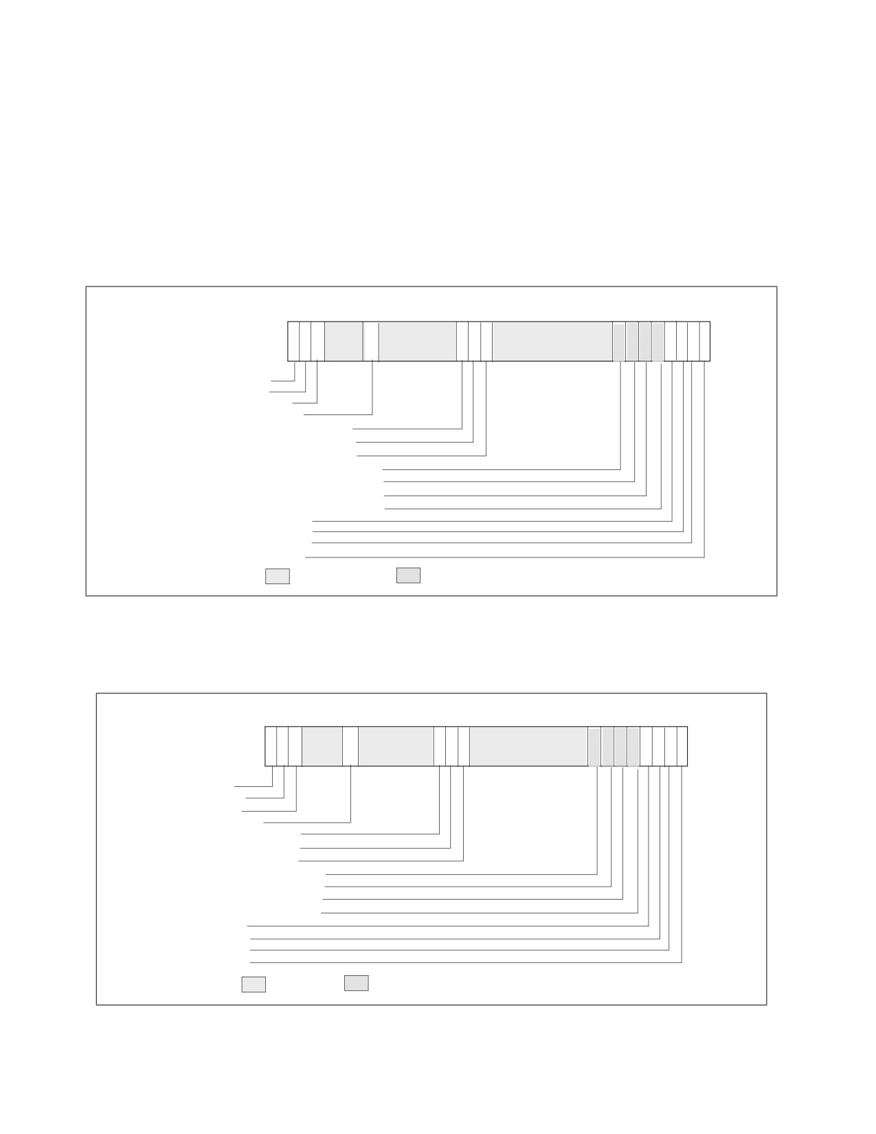
PERFORMANCE MONITORING
20.3.7
5th Generation Intel® Core™ Processor and Intel® Core™ M Processor Performance
Monitoring Facility
The 5th Generation Intel® Core™ processor and the Intel® Core™ M processor families are based on the Broadwell
microarchitecture. The core PMU supports architectural performance monitoring capability with version ID 3 (see
Section 20.2.3) and a host of non-architectural monitoring capabilities.
Architectural performance monitoring version 3 capabilities are described in Section 20.2.3.
The core PMU has the same capability as those described in Section 20.3.6. IA32_PERF_GLOBAL_STATUS provide
a bit indicator (bit 55) for PMI handler to distinguish PMI due to output buffer overflow condition due to accumu-
lating packet data from Intel Processor Trace.
636261
55
3534333231
87
6 5
4 3
2 10
CondChgd
Ovf_Buffer
Ovf_UncorePMU
Trace_ToPA_PMI
FIXED_CTR2 Overflow (RO)
FIXED_CTR1 Overflow (RO)
FIXED_CTR0 Overflow (RO)
PMC7_OVF (RO, If PMC7 present)
PMC6_OVF (RO, If PMC6 present)
PMC5_OVF (RO, If PMC5 present)
PMC4_OVF (RO, If PMC4 present)
PMC3_OVF (RO)
PMC2_OVF (RO)
PMC1_OVF (RO)
PMC0_OVF (RO)
Reserved
Valid if CPUID.0AH:EAX[15:8] = 8; else reserved
Figure 20-35. IA32_PERF_GLOBAL_STATUS MSR in Broadwell Microarchitecture
Details of Intel Processor Trace is described in Chapter 33, “Intel® Processor Trace.” The
IA32_PERF_GLOBAL_OVF_CTRL MSR provides a corresponding reset control bit.
636261
55
3534333231
87
6 5
43
2 10
ClrCondChgd
ClrOvfDSBuffer
ClrOvfUncore
ClrTraceToPA_PMI
FIXED_CTR2 ClrOverflow
FIXED_CTR1 ClrOverflow
FIXED_CTR0 ClrOverflow
PMC7_ClrOvf (if PMC7 present)
PMC6_ClrOvf (if PMC6 present)
PMC5_ClrOvf (if PMC5 present)
PMC4_ClrOvf (if PMC4 present)
PMC3_ClrOvf
PMC2_ClrOvf
PMC1_ClrOvf
PMC0_ClrOvf
Reserved
Valid if CPUID.0AH:EAX[15:8] = 8; else reserved
Figure 20-36. IA32_PERF_GLOBAL_OVF_CTRL MSR in Broadwell microarchitecture
20-56
Vol. 3B

PERFORMANCE MONITORING
The specifics of non-architectural performance events can be found at: https://perfmon-events.intel.com/.
20.3.8
6th Generation, 7th Generation and 8th Generation Intel® Core™ Processor
Performance Monitoring Facility
The 6th generation Intel® Core™ processor is based on the Skylake microarchitecture. The 7th generation Intel®
Core™ processor is based on the Kaby Lake microarchitecture. The 8th generation Intel® Core™ processors, 9th
generation Intel® Core™ processors, and Intel® Xeon® E processors are based on the Coffee Lake microarchitec-
ture. For these microarchitectures, the core PMU supports architectural performance monitoring capability with
version ID 4 (see Section 20.2.4) and a host of non-architectural monitoring capabilities.
Architectural performance monitoring version 4 capabilities are described in Section 20.2.4.
The core PMU’s capability is similar to those described in Section 20.6.3 through Section 20.3.4.5, with some differ-
ences and enhancements summarized in Table 20-33. Additionally, the core PMU provides some enhancement to
support performance monitoring when the target workload contains instruction streams using Intel® Transactional
Synchronization Extensions (TSX), see Section 20.3.6.5. For details of Intel TSX, see Chapter 16, “Programming
with Intel® Transactional Synchronization Extensions‚” of Intel® 64 and IA-32 Architectures Software Developer’s
Manual, Volume 1.
Performance monitoring result may be affected by side-band activity on processors that support Intel SGX, details
are described in Chapter 40, “Enclave Code Debug and Profiling.”
Table 20-33. Core PMU Comparison
Box
Skylake, Kaby Lake and Coffee Lake
Haswell and Broadwell
Comment
Microarchitectures
Microarchitectures
# of Fixed counters per thread
3
3
Use CPUID to
determine # of
counters. See
Section 20.2.1.
# of general-purpose counters
8
8
Use CPUID to
per core
determine # of
counters. See
Section 20.2.1.
Counter width (R,W)
R:48, W: 32/48
R:48, W: 32/48
See Section 20.2.2.
# of programmable counters
4 or (8 if a core not shared by two
4 or (8 if a core not shared by two
Use CPUID to
per thread
threads)
threads)
determine # of
counters. See
Section 20.2.1.
Architectural Perfmon version
4
3
See Section 20.2.4
PMI Overhead Mitigation
• Freeze_Perfmon_on_PMI with
• Freeze_Perfmon_on_PMI with
See Section 18.4.7.
streamlined semantics.
legacy semantics.
Legacy semantics
• Freeze_LBR_on_PMI with
• Freeze_LBR_on_PMI with
not supported with
streamlined semantics.
legacy semantics for branch
version 4 or higher.
• Freeze_while_SMM.
profiling.
• Freeze_while_SMM.
Counter and Buffer Overflow
• Query via
• Query via
See Section 20.2.4.
Status Management
IA32_PERF_GLOBAL_STATUS
IA32_PERF_GLOBAL_STATUS
• Reset via
• Reset via
IA32_PERF_GLOBAL_STATUS_RESET
IA32_PERF_GLOBAL_OVF_CTRL
• Set via
IA32_PERF_GLOBAL_STATUS_SET
Vol. 3B
20-57

PERFORMANCE MONITORING
Table 20-33. Core PMU Comparison (Contd.)
Box
Skylake, Kaby Lake and Coffee Lake
Haswell and Broadwell
Comment
Microarchitectures
Microarchitectures
IA32_PERF_GLOBAL_STATUS
• Individual counter overflow
• Individual counter overflow
See Section 20.2.4.
Indicators of
• PEBS buffer overflow
• PEBS buffer overflow
Overflow/Overhead/Interferen
• ToPA buffer overflow
• ToPA buffer overflow
• CTR_Frz, LBR_Frz, ASCI
(applicable to Broadwell
ce
microarchitecture)
Enable control in
• CTR_Frz
NA
See Section
IA32_PERF_GLOBAL_STATUS
• LBR_Frz
20.2.4.1.
Perfmon Counter In-Use
Query IA32_PERF_GLOBAL_INUSE
NA
See Section
Indicator
20.2.4.3.
Precise Events
See Table 20-36.
See Table 20-12.
IA32_PMC4-PMC7
do not support
PEBS.
PEBS for front end events
See Section 20.3.8.2.
No
LBR Record Format Encoding
000101b
000100b
Section 18.4.8.1
LBR Size
32 entries
16 entries
LBR Entry
From_IP/To_IP/LBR_Info triplet
From_IP/To_IP pair
Section 18.12
LBR Timing
Yes
No
Section 18.12.1
Call Stack Profiling
Yes, see Section 18.11
Yes, see Section 18.11
Use LBR facility.
Off-core Response Event
MSR 1A6H and 1A7H; Extended request
MSR 1A6H and 1A7H; Extended
and response types.
request and response types.
Intel TSX support for Perfmon
See Section 20.3.6.5.
See Section 20.3.6.5.
20.3.8.1 Processor Event Based Sampling (PEBS) Facility
The PEBS facility in the 6th generation, 7th generation and 8th generation Intel Core processors provides a number
enhancement relative to PEBS in processors based on Haswell/Broadwell microarchitectures. The key components
and differences of PEBS facility relative to Haswell/Broadwell microarchitecture is summarized in Table 20-34.
Table 20-34. PEBS Facility Comparison
Box
Skylake, Kaby Lake and
Haswell and Broadwell
Comment
Coffee Lake
Microarchitectures
Microarchitectures
Valid IA32_PMCx
PMC0-PMC3
PMC0-PMC3
No PEBS on PMC4-PMC7.
PEBS Buffer Programming
Section 20.3.1.1.1
Section 20.3.1.1.1
Unchanged
IA32_PEBS_ENABLE Layout
Figure 20-15
Figure 20-15
PEBS-EventingIP
Yes
Yes
PEBS record format encoding
0011b
0010b
PEBS record layout
Table 20-35; enhanced fields
Table 20-24; enhanced fields at
at offsets 98H- B8H; and TSC
offsets 98H, A0H, A8H, B0H.
record field at C0H.
Multi-counter PEBS
PEBS record 90H resolves the
PEBS record 90H reflects
resolution
eventing counter overflow.
IA32_PERF_GLOBAL_STATUS.
Precise Events
See Table 20-36.
See Table 20-12.
IA32_PMC4-IA32_PMC7 do not
support PEBS.
20-58
Vol. 3B

PERFORMANCE MONITORING
Table 20-34. PEBS Facility Comparison (Contd.)
Box
Skylake, Kaby Lake and
Haswell and Broadwell
Comment
Coffee Lake
Microarchitectures
Microarchitectures
PEBS-PDIR
Yes
Yes
IA32_PMC1 only.
PEBS-Load Latency
See Section 20.3.4.4.2.
See Section 20.3.4.4.2.
Data Address Profiling
Yes
Yes
FrontEnd event support
FrontEnd_Retried event and
No
IA32_PMC0-PMC3 only.
MSR_PEBS_FRONTEND.
Only IA32_PMC0 through IA32_PMC3 support PEBS.
NOTES
Precise events are only valid when the following fields of IA32_PERFEVTSELx are all zero:
AnyThread, Edge, Invert, CMask.
In a PMU with PDIR capability, PEBS behavior is unpredictable if IA32_PERFEVTSELx or IA32_PMCx
is changed for a PEBS-enabled counter while an event is being counted. To avoid this, changes to
the programming or value of a PEBS-enabled counter should be performed when the counter is
disabled.
20.3.8.1.1 PEBS Data Format
The PEBS record format for the 6th generation, 7th generation and 8th generation Intel Core processors is
reporting with encoding 0011b in IA32_PERF_CAPABILITIES[11:8]. The lay out is shown in Table 20-35. The PEBS
record format, along with debug/store area storage format, does not change regardless of whether IA-32e mode is
active or not. CPUID.01H:ECX.DTES64[bit 2] reports whether the processor's DS storage format support is mode-
independent. When set, it uses 64-bit DS storage format.
Table 20-35. PEBS Record Format for the 6th Generation, 7th Generation, and 8th Generation Intel Core Processor
Families
Byte Offset
Field
Byte Offset
Field
00H
R/EFLAGS
68H
R11
08H
R/EIP
70H
R12
10H
R/EAX
78H
R13
18H
R/EBX
80H
R14
20H
R/ECX
88H
R15
28H
R/EDX
90H
Applicable Counter
30H
R/ESI
98H
Data Linear Address
38H
R/EDI
A0H
Data Source Encoding
40H
R/EBP
A8H
Latency value (core cycles)
48H
R/ESP
B0H
EventingIP
50H
R8
B8H
TX Abort Information (Section 20.3.6.5.1)
58H
R9
C0H
TSC
60H
R10
The layout of PEBS records are largely identical to those shown in Table 20-24.
Vol. 3B
20-59

PERFORMANCE MONITORING
The PEBS records at offsets 98H, A0H, and ABH record data gathered from three of the PEBS capabilities in prior
processor generations: load latency facility (Section 20.3.4.4.2), PDIR (Section 20.3.4.4.4), and data address
profiling (Section 20.3.6.3).
In the core PMU of the 6th generation, 7th generation and 8th generation Intel Core processors, load latency facility
and PDIR capabilities and data address profiling are unchanged relative to the 4th generation and 5th generation
Intel Core processors. Similarly, precise store is replaced by data address profiling.
With format 0010b, a snapshot of the IA32_PERF_GLOBAL_STATUS may be useful to resolve the situations when
more than one of IA32_PMICx have been configured to collect PEBS data and two consecutive overflows of the
PEBS-enabled counters are sufficiently far apart in time. It is also possible for the image at 90H to indicate multiple
PEBS-enabled counters have overflowed. In the latter scenario, software cannot to correlate the PEBS record entry
to the multiple overflowed bits.
With PEBS record format encoding 0011b, offset 90H reports the “applicable counter” field, which is a multi-
counter PEBS resolution index allowing software to correlate the PEBS record entry with the eventing PEBS over-
flow when multiple counters are configured to record PEBS records. Additionally, offset C0H captures a snapshot of
the TSC that provides a time line annotation for each PEBS record entry.
20.3.8.1.2 PEBS Events
The list of precise events supported for PEBS in the Skylake, Kaby Lake and Coffee Lake microarchitectures is
shown in Table 20-36.
Table 20-36. Precise Events for the Skylake, Kaby Lake, and Coffee Lake Microarchitectures
Event Name
Event Select
Sub-event
UMask
INST_RETIRED
C0H
PREC_DIST1
01H
ALL_CYCLES2
01H
OTHER_ASSISTS
C1H
ANY
3FH
BR_INST_RETIRED
C4H
CONDITIONAL
01H
NEAR_CALL
02H
ALL_BRANCHES
04H
NEAR_RETURN
08H
NEAR_TAKEN
20H
FAR_BRACHES
40H
BR_MISP_RETIRED
C5H
CONDITIONAL
01H
ALL_BRANCHES
04H
NEAR_TAKEN
20H
FRONTEND_RETIRED
C6H
<Programmable3>
01H
HLE_RETIRED
C8H
ABORTED
04H
RTM_RETIRED
C9H
ABORTED
04H
MEM_INST_RETIRED2
D0H
LOCK_LOADS
21H
SPLIT_LOADS
41H
SPLIT_STORES
42H
ALL_LOADS
81H
ALL_STORES
82H
20-60
Vol. 3B

PERFORMANCE MONITORING
Table 20-36. Precise Events for the Skylake, Kaby Lake, and Coffee Lake Microarchitectures (Contd.)
Event Name
Event Select
Sub-event
UMask
MEM_LOAD_RETIRED4
D1H
L1_HIT
01H
L2_HIT
02H
L3_HIT
04H
L1_MISS
08H
L2_MISS
10H
L3_MISS
20H
HIT_LFB
40H
MEM_LOAD_L3_HIT_RETIRED2
D2H
XSNP_MISS
01H
XSNP_HIT
02H
XSNP_HITM
04H
XSNP_NONE
08H
NOTES:
1. Only available on IA32_PMC1.
2. INST_RETIRED.ALL_CYCLES is configured with additional parameters of cmask = 10 and INV = 1
3. Subevents are specified using MSR_PEBS_FRONTEND, see Section 20.3.8.3
4. Instruction with at least one load uop experiencing the condition specified in the UMask.
20.3.8.1.3 Data Address Profiling
The PEBS Data address profiling on the 6th generation, 7th generation and 8th generation Intel Core processors is
largely unchanged from the prior generation. When the DataLA facility is enabled, the relevant information written
into a PEBS record affects entries at offsets 98H, A0H, and A8H, as shown in Table 20-26.
Table 20-37. Layout of Data Linear Address Information In PEBS Record
Field
Offset
Description
Data Linear
98H
The linear address of the load or the destination of the store.
Address
Store Status
A0H
• DCU Hit (Bit 0): The store hit the data cache closest to the core (L1 cache) if this bit is set, otherwise
the store missed the data cache. This information is valid only for the following store events:
UOPS_RETIRED.ALL (if store is tagged),
MEM_INST_RETIRED.STLB_MISS_STORES,
MEM_INST_RETIRED.ALL_STORES,
MEM_INST_RETIRED.SPLIT_STORES.
• Other bits are zero.
Reserved
A8H
Always zero.
20.3.8.2 Frontend Retired Facility
The Skylake Core PMU has been extended to cover common microarchitectural conditions related to the front end
pipeline in addition to providing a generic latency mechanism that can locate fetch bubbles without necessarily
attributing them to a particular condition. The facility counts the events if the associated instruction reaches retire-
ment (architecturally committed). Additionally, the user may opt to enable the PEBS facility to obtain precise infor-
mation on the context of the event, e.g., EventingIP.
The supported frontend microarchitectural conditions require the following interfaces:
• The IA32_PERFEVTSELx MSR must select the FRONTEND_RETIRED event, EventSelect = C6H and UMASK =
01H.
Vol. 3B
20-61

PERFORMANCE MONITORING
• This event employs a new MSR, MSR_PEBS_FRONTEND, to specify the supported frontend event details, see
Table 20-38.
• If precise information is desired, program the PEBS_EN_PMCx field of IA32_PEBS_ENABLE MSR as required.
Note the AnyThread field of IA32_PERFEVTSELx is ignored by the processor for the “FRONTEND_RETIRED” event.
The sub-event encodings supported by MSR_PEBS_FRONTEND.EVTSEL is given in Table 20-38.
Table 20-38. FrontEnd_Retired Sub-Event Encodings Supported by MSR_PEBS_FRONTEND.EVTSEL
Sub-Event Name
EVTSEL
Description
ANY_DSB_MISS
1H
Retired Instructions which experienced any decode stream buffer (DSB) miss.
DSB_MISS
11H
Retired Instructions which experienced a DSB miss that caused a fetch starvation cycle.
L1I_MISS
12H
The fetch of retired Instructions which experienced Instruction L1 Cache true miss1. Additional
requests to the same cache line as an in-flight L1I cache miss will not be counted.
L2_MISS
13H
The fetch of retired Instructions which experienced L2 Cache true miss. Additional requests to the
same cache line as an in-flight MLC cache miss will not be counted.
ITLB_MISS
14H
The fetch of retired Instructions which experienced ITLB true miss. Additional requests to the same
cache line as an in-flight ITLB miss will not be counted.
STLB_MISS
15H
The fetch of retired Instructions which experienced STLB true miss. Additional requests to the
same cache line as an in-flight STLB miss will not be counted.
IDQ_READ_BUBBLES
6H
An IDQ read bubble is defined as any one of the 4 allocation slots of IDQ that is not filled by the
front-end on any cycle where there is no back end stall. Using the threshold and latency fields in
MSR_PEBS_FRONTEND allows counting of IDQ read bubbles of various magnitude and duration.
Latency controls the number of cycles and Threshold controls the number of allocation slots that
contain bubbles.
The event counts if and only if a sequence of at least FE_LATENCY consecutive cycles contain at
least FE_TRESHOLD number of bubbles each.
NOTES:
1. A true miss is the first miss for a cacheline/page (excluding secondary misses that fall into same cacheline/page).
The layout of MSR_PEBS_FRONTEND is given in Table 20-39.
Table 20-39. MSR_PEBS_FRONTEND Layout
Bit Name
Offset
Description
EVTSEL
7:0
Encodes the sub-event within FrontEnd_Retired that can use PEBS facility, see Table 20-38.
IDQ_Bubble_Length
19:8
Specifies the threshold of continuously elapsed cycles for the specified width of bubbles when
counting IDQ_READ_BUBBLES event.
IDQ_Bubble_Width
22:20
Specifies the threshold of simultaneous bubbles when counting IDQ_READ_BUBBLES event.
Reserved
63:23
Reserved
The FRONTEND_RETIRED event is designed to help software developers identify exact instructions that caused
front-end issues. There are some instances in which the event will, by design, the under-counting scenarios include
the following:
• The event counts only retired (non-speculative) front-end events, i.e., events from just true program execution
path are counted.
• The event will count once per cacheline (at most). If a cacheline contains multiple instructions which caused
front-end misses, the count will be only 1 for that line.
• If the multibyte sequence of an instruction spans across two cachelines and causes a miss it will be recorded
once. If there were additional misses in the second cacheline, they will not be counted separately.
20-62
Vol. 3B

PERFORMANCE MONITORING
• If a multi-uop instruction exceeds the allocation width of one cycle, the bubbles associated with these uops will
be counted once per that instruction.
• If 2 instructions are fused (macro-fusion), and either of them or both cause front-end misses, it will be counted
once for the fused instruction.
• If a front-end (miss) event occurs outside instruction boundary (e.g., due to processor handling of architectural
event), it may be reported for the next instruction to retire.
20.3.8.3 Off-core Response Performance Monitoring
The core PMU facility to collect off-core response events are similar to those described in Section 20.3.4.5. Each
event code for off-core response monitoring requires programming an associated configuration MSR, MSR_OFF-
CORE_RSP_x. Software must program MSR_OFFCORE_RSP_x according to:
• Transaction request type encoding (bits 15:0): see Table 20-40.
• Supplier information (bits 29:16): see Table 20-41.
• Snoop response information (bits 37:30): see Table 20-42.
Table 20-40. MSR_OFFCORE_RSP_x Request_Type Definition
(Skylake, Kaby Lake, and Coffee Lake Microarchitectures)
Bit Name
Offset
Description
DMND_DATA_RD
0
Counts the number of demand data reads and page table entry cacheline reads. Does not count hw or
sw prefetches.
DMND_RFO
1
Counts the number of demand reads for ownership (RFO) requests generated by a write to data
cacheline. Does not count L2 RFO prefetches.
DMND_IFETCH
2
Counts the number of demand instruction cacheline reads and L1 instruction cacheline prefetches.
Reserved
14:3
Reserved
OTHER
15
Counts miscellaneous requests, such as I/O and uncacheable accesses.
Table 20-41 lists the supplier information field that applies to 6th generation, 7th generation and 8th generation
Intel Core processors. (6th generation Intel Core processor CPUID signatures: 06_4EH and 06_5EH; 7th genera-
tion and 8th generation Intel Core processor CPUID signatures: 06_8EH and 06_9EH).
Table 20-41. MSR_OFFCORE_RSP_x Supplier Info Field Definition
(CPUID Signatures: 06_4EH, 06_5EH, 06_8EH, 06_9EH)
Subtype
Bit Name
Offset
Description
Common
Any
16
Catch all value for any response types.
Supplier
NO_SUPP
17
No Supplier Information available.
Info
L3_HITM
18
M-state initial lookup stat in L3.
L3_HITE
19
E-state
L3_HITS
20
S-state
Reserved
21
Reserved
L4_HIT
22
L4 Cache (if L4 is present in the processor).
Reserved
25:23
Reserved
DRAM
26
Local Node
Reserved
29:27
Reserved
SPL_HIT
30
L4 cache super line hit (if L4 is present in the processor).
Vol. 3B
20-63

PERFORMANCE MONITORING
Table 20-42 lists the snoop information field that apply to processors with CPUID signatures 06_4EH, 06_5EH,
06_8EH, 06_9E, and 06_55H.
Table 20-42. MSR_OFFCORE_RSP_x Snoop Info Field Definition
(CPUID Signatures: 06_4EH, 06_5EH, 06_8EH, 06_9E, 06_55H)
Subtype
Bit Name
Offset
Description
Snoop Info
SPL_HIT
30
L4 cache super line hit (if L4 is present in the processor).
SNOOP_NONE
31
No details on snoop-related information.
SNOOP_NOT_NEEDED
32
No snoop was needed to satisfy the request.
SNOOP_MISS
33
A snoop was needed and it missed all snooped caches:
-For LLC Hit, ReslHitl was returned by all cores.
-For LLC Miss, Rspl was returned by all sockets and data was returned from
DRAM.
SNOOP_HIT_NO_FWD
34
A snoop was needed and it hits in at least one snooped cache. Hit denotes a
cache-line was valid before snoop effect. This includes:
-Snoop Hit w/ Invalidation (LLC Hit, RFO).
-Snoop Hit, Left Shared (LLC Hit/Miss, IFetch/Data_RD).
-Snoop Hit w/ Invalidation and No Forward (LLC Miss, RFO Hit S).
In the LLC Miss case, data is returned from DRAM.
SNOOP_HIT_WITH_FWD
35
A snoop was needed and data was forwarded from a remote socket. This
includes:
-Snoop Forward Clean, Left Shared (LLC Hit/Miss, IFetch/Data_RD/RFT).
SNOOP_HITM
36
A snoop was needed and it HitM-ed in local or remote cache. HitM denotes a
cache-line was in modified state before effect as a results of snoop. This
includes:
-Snoop HitM w/ WB (LLC miss, IFetch/Data_RD).
-Snoop Forward Modified w/ Invalidation (LLC Hit/Miss, RFO).
-Snoop MtoS (LLC Hit, IFetch/Data_RD).
SNOOP_NON_DRAM
37
Target was non-DRAM system address. This includes MMIO transactions.
20.3.8.3.1
Off-core Response Performance Monitoring for the Intel® Xeon® Scalable Processor Family
The following tables list the requestor and supplier information fields that apply to the Intel® Xeon® Scalable
Processor Family.
• Transaction request type encoding (bits 15:0): see Table 20-43.
• Supplier information (bits 29:16): see Table 20-44.
• Supplier information (bits 29:16) with support for Intel® Optane™ DC Persistent Memory support: see
Table 20-45.
• Snoop response information has not been changed and is the same as in (bits 37:30): see Table 20-42.
20-64
Vol. 3B

PERFORMANCE MONITORING
Table 20-43. MSR_OFFCORE_RSP_x Request_Type Definition (Intel® Xeon® Scalable Processor Family)
Bit Name
Offset
Description
DEMAND_DATA_RD
0
Counts the number of demand data reads and page table entry cacheline reads. Does not count
hw or sw prefetches.
DEMAND_RFO
1
Counts the number of demand reads for ownership (RFO) requests generated by a write to data
cacheline. Does not count L2 RFO prefetches.
DEMAND_CODE_RD
2
Counts the number of demand instruction cacheline reads and L1 instruction cacheline
prefetches.
Reserved
3
Reserved.
PF_L2_DATA_RD
4
Counts the number of prefetch data reads into L2.
PF_L2_RFO
5
Counts the number of RFO Requests generated by the MLC prefetches to L2.
Reserved
6
Reserved.
PF_L3_DATA_RD
7
Counts the number of MLC data read prefetches into L3.
PF_L3_RFO
8
Counts the number of RFO requests generated by MLC prefetches to L3.
Reserved
9
Reserved.
PF_L1D_AND_SW
10
Counts data cacheline reads generated by hardware L1 data cache prefetcher or software
prefetch requests.
Reserved
14:11
Reserved.
OTHER
15
Counts miscellaneous requests, such as I/O and un-cacheable accesses.
Table 20-44 lists the supplier information field that applies to the Intel Xeon Scalable Processor Family (CPUID
signature: 06_55H).
Table 20-44. MSR_OFFCORE_RSP_x Supplier Info Field Definition (CPUID Signature: 06_55H)
Subtype
Bit Name
Offset
Description
Common
Any
16
Catch all value for any response types.
Supplier
SUPPLIER_NONE
17
No Supplier Information available.
Info
L3_HIT_M
18
M-state initial lookup stat in L3.
L3_HIT_E
19
E-state
L3_HIT_S
20
S-state
L3_HIT_F
21
F-state
Reserved
25:22
Reserved
L3_MISS_LOCAL_DRAM
26
L3 Miss: local home requests that missed the L3 cache and were
serviced by local DRAM.
L3_MISS_REMOTE_HOP0_DRAM
27
Hop 0 Remote supplier.
L3_MISS_REMOTE_HOP1_DRAM
28
Hop 1 Remote supplier.
L3_MISS_REMOTE_HOP2P_DRAM
29
Hop 2 or more Remote supplier.
Reserved
30
Reserved
Table 20-45 lists the supplier information field that applies to the Intel Xeon Scalable Processor Family (CPUID
signature: 06_55H, Steppings 0x5H - 0xFH).
Vol. 3B
20-65

PERFORMANCE MONITORING
Table 20-45. MSR_OFFCORE_RSP_x Supplier Info Field Definition
(CPUID Signature: 06_55H, Steppings 0x5H - 0xFH)
Subtype
Bit Name
Offset
Description
Common
Any
16
Catch all value for any response types.
Supplier
SUPPLIER_NONE
17
No Supplier Information available.
Info
L3_HIT_M
18
M-state initial lookup stat in L3.
L3_HIT_E
19
E-state
L3_HIT_S
20
S-state
L3_HIT_F
21
F-state
LOCAL_PMM
22
Local home requests that were serviced by local PMM.
REMOTE_HOP0_PMM
23
Hop 0 Remote supplier.
REMOTE_HOP1_PMM
24
Hop 1 Remote supplier.
REMOTE_HOP2P_PMM
25
Hop 2 or more Remote supplier.
L3_MISS_LOCAL_DRAM
26
L3 Miss: Local home requests that missed the L3 cache and were
serviced by local DRAM.
L3_MISS_REMOTE_HOP0_DRAM
27
Hop 0 Remote supplier.
L3_MISS_REMOTE_HOP1_DRAM
28
Hop 1 Remote supplier.
L3_MISS_REMOTE_HOP2P_DRAM
29
Hop 2 or more Remote supplier.
Reserved
30
Reserved
20.3.8.4
Uncore Performance Monitoring Facilities on Intel® Core™ Processors Based on Cannon Lake
Microarchitecture
Cannon Lake microarchitecture introduces LLC support of up to six processor cores. To support six processor cores
and eight LLC slices, existing MSRs have been rearranged and new CBo MSRs have been added. Uncore perfor-
mance monitoring software drivers from prior generations of Intel Core processors will need to update the MSR
addresses. The new MSRs and updated MSR addresses have been added to the Uncore PMU listing in Section
2.17.2, “MSRs Specific to 8th Generation Intel® Core™ i3 Processors,” in Intel® 64 and IA-32 Architectures Soft-
ware Developer’s Manual, Volume 4.
20.3.9
10th Generation Intel® Core™ Processor Performance Monitoring Facility
Some 10th generation Intel® Core™ processors and some 3rd generation Intel® Xeon® Scalable Processor Family
are based on Ice Lake microarchitecture. Some 11th generation Intel® Core™ processors are based on the Tiger
Lake microarchitecture, and some are based on the Rocket Lake microarchitecture. For these processors, the core
PMU supports architectural performance monitoring capability with version Id 5 (see Section 20.2.5) and a host of
non-architectural monitoring capabilities.
The core PMU's capability is similar to those described in Section 20.3.1 through Section 20.3.8, with some differ-
ences and enhancements summarized in Table 20-46.
20-66
Vol. 3B

PERFORMANCE MONITORING
Table 20-46. Core PMU Summary of the Ice Lake Microarchitecture
Box
Ice Lake Microarchitecture
Skylake, Kaby Lake and Coffee
Comment
Lake Microarchitectures
Architectural Perfmon
5
4
See Section 20.2.5.
version
Number of programmable
8
4
Use CPUID to determine number
counters per thread
of counters. See Section 20.2.1.
PEBS: Basic functionality
Yes
Yes
See Section 20.3.9.1.
PEBS record format encoding
0100b
0011b
See Section 20.6.2.4.2.
Extended PEBS
PEBS is extended to all Fixed
No
See Section 20.9.1.
and General Purpose counters
and to all performance
monitoring events.
Adaptive PEBS
Yes
No
See Section 20.9.2.
Performance Metrics
Yes (4)
No
See Section 20.3.9.3.
PEBS-PDIR
IA32_FIXED0 only
IA32_PMC1 only.
(Corresponding counter control
MSRs must be enabled.)
20.3.9.1 Processor Event Based Sampling (PEBS) Facility
The PEBS facility in the 10th generation Intel Core processors provides a number of enhancements relative to PEBS
in processors based on the Skylake, Kaby Lake, and Coffee Lake microarchitectures. Enhancement of the PEBS
facility with Extended PEBS and Adaptive PEBS features is described in detail in Section 20.9.
The 3rd generation Intel Xeon Scalable Family of processors based on the Ice Lake microarchitecture introduce
EPT-friendly PEBS. This allows EPT violations and other VM Exits to be taken on PEBS accesses to the DS Area. See
Section 20.9.5 for details.
20.3.9.2 Off-core Response Performance Monitoring
The core PMU facility to collect off-core response events are similar to those described in Section 20.3.4.5. Each
event code for off-core response monitoring requires programming an associated configuration MSR, MSR_OFF-
CORE_RSP_x. Software must program MSR_OFFCORE_RSP_x according to:
• Transaction request type encoding (bits 15:0): see Table 18-[N1].
• Response type encoding (bits 16-37) of
— Supplier information: see Table [18-N2].
— Snoop response information: see Table [18-N3].
• All transactions are tracked at cacheline granularity except some in request type OTHER.
Table 20-47. MSR_OFFCORE_RSP_x Request_Type Definition
(Processors Based on Ice Lake Microarchitecture)
Bit Name
Offset
Description
DEMAND_DATA_RD
0
Counts demand data and page table entry reads.
DEMAND_RFO
1
Counts demand read (RFO) and software prefetches (PREFETCHW) for exclusive ownership
in anticipation of a write.
DEMAND_CODE_RD
2
Counts demand instruction fetches and instruction prefetches targeting the L1 instruction
cache.
Reserved
3
Reserved
Vol. 3B
20-67

PERFORMANCE MONITORING
Table 20-47. MSR_OFFCORE_RSP_x Request_Type Definition
(Processors Based on Ice Lake Microarchitecture)
Bit Name
Offset
Description
HWPF_L2_DATA_RD
4
Counts hardware generated data read prefetches targeting the L2 cache.
HWPF_L2_RFO
5
Counts hardware generated prefetches for exclusive ownership (RFO) targeting the L2
cache.
Reserved
6
Reserved
HWPF_L3
9:7 and 131
Counts hardware generated prefetches of any type targeting the L3 cache.
HWPF_L1D_AND_SWPF
10
Counts hardware generated data read prefetches targeting the L1 data cache and the
following software prefetches (PREFETCHNTA, PREFETCHT0/1/2).
STREAMING_WR
11
Counts streaming stores.
Reserved
12
Reserved
Reserved
14
Reserved
OTHER
15
Counts miscellaneous requests, such as I/O and un-cacheable accesses.
NOTES:
1. All bits need to be set to 1 to count this type.
Ice Lake microarchitecture has added a new category of Response subtype, called a Combined Response Info. To
count a feature in this type, all the bits specified must be set to 1.
A valid response type must be a non-zero value of the following expression:
Any | ['OR' of Combined Response Info Bits | [('OR' of Supplier Info Bits) & ('OR' of Snoop Info Bits)]]
If "ANY" bit[16] is set, other response type bits [17-39] are ignored.
Table 20-48 lists the supplier information field that applies to processors based on Ice Lake microarchitecture.
Table 20-48. MSR_OFFCORE_RSP_x Supplier Info Field Definition
(Processors Based on Ice Lake Microarchitecture)
Subtype
Bit Name
Offset
Description
Common
Any
16
Catch all value for any response types.
Combined
DRAM
26, 31, 321
Requests that are satisfied by DRAM.
Response
NON_DRAM
26, 371
Requests that are satisfied by a NON_DRAM system component. This includes
Info
MMIO transactions.
L3_MISS
22, 23, 24, 25, 26, 27,
Requests that were not supplied by the L3 Cache. The event includes some
28, 29, 30, 31, 32, 33,
currently reserved bits in anticipation of future memory designs.
34, 35, 36, 371
Supplier
L3_HIT
18,19, 201
Requests that hit in L3 cache. Depending on the snoop response the L3 cache
Info
may have retrieved the cacheline from another core's cache.
Reserved
17, 21:25, 27:29
Reserved.
NOTES:
1. All bits need to be set to 1 to count this type.
Table 20-49 lists the snoop information field that applies to processors based on Ice Lake microarchitecture.
20-68
Vol. 3B

PERFORMANCE MONITORING
Table 20-49. MSR_OFFCORE_RSP_x Snoop Info Field Definition
(Processors Based on Ice Lake Microarchitecture)
Subtype
Bit Name
Offset
Description
Snoop
Reserved
30
Reserved.
Info
SNOOP_NOT_NEEDED
32
No snoop was needed to satisfy the request.
SNOOP_MISS
33
A snoop was sent and none of the snooped caches contained the cacheline.
SNOOP_HIT_NO_FWD
34
A snoop was sent and hit in at least one snooped cache. The unmodified
cacheline was not forwarded back, because the L3 already has a valid copy.
Reserved
35
Reserved.
SNOOP_HITM
36
A snoop was sent and the cacheline was found modified in another core's
caches. The modified cacheline was forwarded to the requesting core.
20.3.9.3 Performance Metrics
The Ice Lake core PMU provides built-in support for Top-down Microarchitecture Analysis (TMA) method level 1
metrics. These metrics are always available to cross-validate performance observations, freeing general purpose
counters to count other events in high counter utilization scenarios. For more details about the method, refer to
Top-Down Analysis Method chapter (Appendix B.1) of the Intel® 64 and IA-32 Architectures Optimization Refer-
ence Manual.
A new MSR called MSR_PERF_METRICS reports the metrics directly. Software can check (and/or expose to its
guests) the availability of the PERF_METRICS feature using IA32_PERF_CAPABILITIES.PERF_METRICS_AVAILABLE
(bit 15). For additional details on this MSR, refer to Chapter 2, “Model-Specific Registers (MSRs)‚” in the Intel® 64
and IA-32 Architectures Software Developer’s Manual, Volume 4.
Reserved
Backend Bound
Frontend Bound
Bad Speculation
Retiring
23
15
7
0
31
55
47
39
63
Figure 20-37. MSR_PERF_METRICS Definition
This register exposes the four TMA Level 1 metrics. The lower 32 bits are divided into four 8-bit fields, as shown by
the above figure, each of which is an integer fraction of 255.
Vol. 3B
20-69

PERFORMANCE MONITORING
To support built-in performance metrics, new bits have been added to the following MSRs:
• IA32_PERF_GLOBAL_CTRL. EN_PERF_METRICS[48]: If this bit is set and fixed-function performance-
monitoring counter 3 is enabled, built-in performance metrics are enabled.
• IA32_PERF_GLOBAL_STATUS_SET. SET_OVF_PERF_METRICS[48]: If this bit is set, it will set the status bit in
the IA32_PERF_GLOBAL_STATUS register for PERF_METRICS.
• IA32_PERF_GLOBAL_STATUS_RESET. RESET_OVF_PERF_METRICS[48]: If this bit is set, it will clear the status
bit in the IA32_PERF_GLOBAL_STATUS register for PERF_METRICS.
• IA32_PERF_GLOBAL_STATUS. OVF_PERF_METRICS[48]: If this bit is set, it indicates that a PERF_METRICS-
related resource has overflowed and a PMI is triggered1. If this bit is clear, no such overflow has occurred.
NOTE
Software has to synchronize, e.g., re-start, fixed-function performance-monitoring counter 3 as
well as PERF_METRICS when either bit 35 or 48 in IA32_PERF_GLOBAL_STATUS is set. Otherwise,
PERF_METRICS may return undefined values.
The values in MSR_PERF_METRICS are derived from fixed-function performance-monitoring counter 3. Software
should start both registers, PERF_METRICS and fixed-function performance-monitoring counter 3, from zero. Addi-
tionally, software is recommended to periodically clear both registers in order to maintain accurate measurements
for certain scenarios that involve sampling metrics at high rates.
In order to save/restore PERF_METRICS, software should follow these guidelines:
• PERF_METRICS and fixed-function performance-monitoring counter 3 should be saved and restored together.
• To ensure that PERF_METRICS and fixed-function performance-monitoring counter 3 remain synchronized,
both should be disabled during both save and restore. Software should enable/disable them atomically, with a
single write to IA32_PERF_GLOBAL_CTRL to set/clear both EN_PERF_METRICS[bit 48] and
EN_FIXED_CTR3[bit 35].
• On state restore, fixed-function performance-monitoring counter 3 must be restored before PERF_METRICS,
otherwise undefined results may be observed.
20.3.10
12th and 13th Generation Intel® Core™ Processors, and 4th Generation Intel® Xeon®
Scalable Processor Family Performance Monitoring Facility
The 12th generation Intel® Core™ processor supports Alder Lake performance hybrid architecture. These proces-
sors offer a unique combination of Performance and Efficient-cores (P-core and E-core). The P-core is based on
Golden Cove microarchitecture and the E-core is based on Gracemont microarchitecture. The 13th generation
Intel® Core™ processor supports Raptor Lake performance hybrid architecture, utilizing both Raptor Cove cores
and enhanced Gracemont cores. The 4th generation Intel® Xeon® Scalable Processor Family is based on Sapphire
Rapids microarchitecture utilizing Golden Cove cores. These processors all report architectural performance moni-
toring version ID = 5 and support non-architectural monitoring capabilities described in this section.
20.3.10.1 P-core Performance Monitoring Unit
The P-core PMU's capability is similar to those described in Section 20.3.1 through Section 20.3.9, with some differ-
ences and enhancements summarized in Table 20-50.
1. An overflow of fixed-function performance-monitoring counter 3 should normally happen first if software follows Intel’s recommen-
dations.
20-70
Vol. 3B

PERFORMANCE MONITORING
Table 20-50. Core PMU Summary of the Golden Cove Microarchitecture
Box
Golden Cove
Ice Lake Microarchitecture
Comment
Microarchitecture
Architectural Perfmon
5
5
See Section 20.2.5.
version
Event-Counter Restrictions
Simplified identification
Counters 4-7 support a subset of
events. See Section 20.3.10.1.2.
Performance Metrics
Yes (12)
Yes (4)
See Section 20.3.9.3.
PEBS: Baseline, record
Yes
Yes
See Section 20.3.9.
format
0100b
0100b
PEBS: EPT-friendly
Yes
No; debuts in Ice Lake server
See Section 20.6.2.4.2.
microarchitecture
PEBS: Precise Distribution
IA32_FIXED0 instruction-
IA32_FIXED0 cycle-granularity
See Section 20.9.6.
granularity
PDist on IA32_PMC0
No PDist
PEBS: Load Latency
Instruction latency
Instruction latency
See Section 20.9.7.
Cache latency
Access info fields (5)
Access info fields (3)
PEBS: Store Latency
Cache latency
None
See Section 20.9.8.
Access info fields (3)
PEBS: Intel TSX support
Abort info fields (9)
Abort info fields (8)
See Section 20.3.6.5.1.
(Intel Xeon processor only
feature.)
20.3.10.1.1 P-core Perf Metrics Extensions
For 12th generation Intel Core processor P-cores, the core PMU supports the built-in metrics that were introduced
in the Ice Lake microarchitecture PMU. This core PMU extends the PERF_METRICS MSR to feature TMA method
level 2 metrics, as shown in Figure 20-38.
Backend Bound
Frontend Bound
Bad Speculation
Retiring
31
23
15
7
0
Memory Bound
Fetch Latency
Branch Mispredicts
Heavy Operations
63
55
47
39
32
Figure 20-38. PERF_METRICS MSR Definition for 12th Generation Intel® Core™ Processor P-core
Vol. 3B
20-71

PERFORMANCE MONITORING
The lower half of the register is the TMA level 1 metrics (legacy). The upper half is also divided into four 8-bit fields,
each of which is an integer fraction of 255. Additionally, each of the new level 2 metrics in the upper half is a subset
of the corresponding level 1 metric in the lower half (that is, its parent node per the TMA hierarchy). This enables
software to deduce the other four level 2 metrics by subtracting corresponding metrics as shown in Figure 20-39.
Ligh t_O perations = Re tirin g - Heavy_ Opera tion s
Machine_Clears = Bad_Speculation - Branch_Mispredicts
Fetch_Bandwidth = Frontend_Bound - Fetch_Latency
Core_Bound = Backend_Bound - Memory_Bound
Figure 20-39. Deducing Implied Level 2 Metrics in the Core PMU for12th Generation Intel® Core™ Processor P-core
The PERF_METRICS MSR and fixed-function performance-monitoring counter 3 of the core PMU feature 12 metrics
in total that cover all level 1 and level 2 nodes of the TMA hierarchy.
20.3.10.1.2 P-core Counter Restrictions Simplification
The 12th generation Intel Core processor P-core allows identification of performance monitoring events with
counter restrictions based on event encodings. The general rule is: Event Codes < 0x90 are restricted to general-
purpose performance-monitoring counters 0-3. Event Codes ≥ 0x90 are likely to have no restrictions. Table 20-51
lists the exceptions to this rule.
Table 20-51. Special Performance Monitoring Events with Counter Restrictions
Event Encoding1
Event Name
Counter Restriction
xx3C
CPU_CLK_UNHALTED.*
0-7 (No restriction for all architectural events.)
xx2E
LONGEST_LAT_CACHE.*
xxDx
MEM_*_RETIRED.*
0-3
01A3, 02A3, 08A3
Some CYCLE_ACTIVITY sub-events
0-3
02CD
MEM_TRANS_RETIRED.STORE_SAMPLE
0
04A4
TOPDOWN.BAD_SPEC_SLOTS
0
08A4
TOPDOWN.BR_MISPREDICT_SLOTS
xxCE
AMX_OPS_RETIRED
0
NOTES:
1. Linux perf rUUEE syntax, where UU is the Unit Mask field and EE is the Event Select (also known as Event
Code) field in the IA32_PERFEVTSELx MSRs.
20.3.10.1.3 P-core Off-core Response Facility
For the 12th generation Intel Core processor P-core, the Off-core Response (OCR) Facility is similar to that
described in Section 20.3.9.2.
The following enhancements are introduced for the Request_Type of MSR_OFFCORE_RSP_x:
• WB (bits 3 and 12): Count writeback (modified or non-modified) transactions by core caches.
• HWPF_L1D (bit 10): Counts hardware generated data read prefetches targeting the L1 data cache (only).
• SWPF_READ (bit 14): Counts software generated data read prefetches by the PREFETCHNTA and
PREFETCHT0/1/2 instructions.
20-72
Vol. 3B

PERFORMANCE MONITORING
20.3.10.2 E-core Performance Monitoring Unit
The core PMU capabilities on the 12th generation Intel Core processor E-core are summarized in Table 20-52
below.
Table 20-52. Core PMU Summary of the Gracemont Microarchitecture
Box
Gracemont
Tremont Microarchitecture
Comment
Microarchitecture
Number of fixed-function
3
3
Use CPUID to enumerate number of
performance-monitoring
counters. See Section 20.2.1.
counters per core
Number of general-purpose
6
4
Use CPUID to enumerate number of
counters per core
counters. See Section 20.2.1.
Architectural Performance
5
5
See Section 20.2.5.
Monitoring version ID
PEBS record format encoding
0100b
0100b
See Section 20.5.5.
EPT-friendly PEBS support
Yes
No
See Section 20.9.5.
Extended PEBS
Yes
Yes
See Section 20.9.1.
Adaptive PEBS
Yes
Yes
See Section 20.9.2.
Precise distribution (PDist) PEBS
IA32_PMC0 and
IA32_PMC0 and
PDist eliminates skid, see Section
IA32_FIXED_CTR0
IA32_FIXED_CTR0
20.9.3, Section 20.9.4, and Section
20.9.6.
PEBS Latency
Load and Store Latency
No
See Section 20.3.10.2.1, Section
20.3.10.2.2, Section 20.9.7, and
Section 20.9.8.
PEBS Output
DS Save Area or Intel®
DS Save Area or Intel®
See Section 20.5.5.2.1.
Processor Trace
Processor Trace
Offcore Response
MSR 01A6H and 01A7H,
MSR 1A6H and 1A7H, each
See Section 20.5.5.4.
each core has its own
core has its own register,
register, extended request
extended request and
and response types.
response types.
20.3.10.2.1 E-core PEBS Load Latency
The 12th generation Intel Core processor E-core includes PEBS Load Latency support similar to that described in
Section 20.9.7.
When a programmable counter is configured to count MEM_UOPS_RETIRED.LOAD_LATENCY_ABOVE_THRESHOLD
(IA32_PERFEVTSELx[15:0] = 0xD005, with CMASK=0 and INV=0), selected load operations whose latency
exceeds the threshold provided in MSR_PEBS_LD_LAT_THRESHOLD (MSR 03F6H) will be counted. If a PEBS record
is generated on overflow of this counter, the Memory Access Latency and Memory Auxiliary Info data is reported in
the Memory Access Info group (Section 20.9.2.2.2). The formats of these fields are shown in Table 20-53 and Table
20-94.
Table 20-53. E-core PEBS Memory Access Info Encoding
Bit(s)
Field
Description
3:0
Data Source
The source of the data; see Table 20-54.
4
Lock
0: The operation was not part of a locked transaction.
1: The operation was part of a locked transaction.
Vol. 3B
20-73

PERFORMANCE MONITORING
Table 20-53. E-core PEBS Memory Access Info Encoding (Contd.)
Bit(s)
Field
Description
5
STLB_MISS
0: The load did not miss the STLB (hit the DTLB or STLB).
1: The load missed the STLB.
6
ST_FWD_BLK
0: Load did not get a store forward block.
1: Load got a store forward block.
63:7
Reserved
Reserved
For details on E-core PEBS memory access latency encoding, see the Access Latency Field in Table 20-94.
Table 20-54. E-core PEBS Data Source Encodings
Encoding
Description
00H
Unknown Data Source (the processor could not retrieve the origin of this request) and MMIO. Memory mapped I/O hit.
01H
L1 HIT. This request was satisfied by the L1 data cache. (Minimal latency core cache hit.)
02H
FB HIT. Outstanding core cache miss to same cache-line address was already underway. (Pending core cache hit.)
03H
L2 HIT. This request was satisfied by the L2 cache.
04H
L3 HIT. Local or Remote home requests that hit L3 cache in the uncore with no coherency actions required (snooping).
05H
L3 HITE. Local or Remote home requests that hit the L3 cache and were serviced by another processor core with a
cross core snoop where no modified copies were found (clean).
06H
L3 HITM. Local or Remote home requests that hit the L3 cache and were serviced by another processor core with a
cross core snoop where a modified copy was found.
07H
Reserved.
08H
L3 HITF. Local or Remote home requests that hit the L3 cache and were serviced by another processor core with a
cross core snoop where a shared or forwarding copy was found.
09H
Reserved.
0AH
L3 MISS. Local home requests that missed the L3 cache and were serviced by local DRAM (go to shared state).
0BH
Reserved.
0CH
Reserved.
0DH
Reserved.
0EH
I/O. Request of input/output operation.
0FH
The request was to un-cacheable memory.
20.3.10.2.2 E-core PEBS Store Latency
The 12th generation Intel Core processor E-core includes PEBS Store Latency support. When a programmable
counter is configured to count MEM_UOPS_RETIRED.STORE_LATENCY (IA32_PERFEVTSELx[15:0] = 0xD006, with
CMASK=0 and INV=0), all store operations will be counted. If a PEBS record is generated on overflow of this
counter, the Memory Access Latency and Memory Auxiliary Info data is reported in the Memory Access Info group
(Section 18.9.2.2.2). The formats of these fields are shown in Table 20-53 and Table 20-94.
20.3.10.2.3 E-core Precise Distribution (PDist) Support
The 12th generation Intel Core processor E-core supports PEBS with Precise Distribution (PDist) on IA32_PMC0 and
IA32_FIXED_CTR0. All precise events support PDist save for UOPS_RETIRED. See Section 20.9.6 for additional
details on PDist.
20-74
Vol. 3B

PERFORMANCE MONITORING
20.3.10.2.4 E-core Enhanced Off-core Response
Event number 0B7H support off-core response monitoring using an associated configuration MSR, MSR_OFF-
CORE_RSP0 (address 1A6H) in conjunction with UMASK value 01H or MSR_OFFCORE_RSP1 (address 1A7H) in
conjunction with UMASK value 02H. There are unique pairs of MSR_OFFCORE_RSPx registers per core. The layout
of MSR_OFFCORE_RSP0 and MSR_OFFCORE_RSP1 are organized as follows:
• Bits 15:0 and bits 49:44 specify the request type of a transaction request to the uncore. This is described in
Table 20-55.
• Bits 30:16 specify Response Type information or an L2 Hit, and is described in Table 20-75.
• If L2 misses, then bits 37:31 can be used to specify snoop response information and is described in Table
20-76.
• For outstanding requests, bit 38 can enable measurement of average latency of specific type of offcore
transaction requests using two programmable counter simultaneously; see Section 20.5.2.3 for details.
Table 20-55. MSR_OFFCORE_RSPx Request Type Definition
Bit Name
Offset
Description
DEMAND_DATA_RD
0
Counts demand data reads.
DEMAND_RFO
1
Counts all demand reads for ownership (RFO) requests and software based prefteches for
exclusive ownership (prefetchw).
DEMAND_CODE_RD
2
Counts demand instruction fetches and L1 instruction cache prefetches.
COREWB_M
3
Counts modified write backs from L1 and L2.
HWPF_L2_DATA_RD
4
Counts prefetch (that bring data to L2) data reads.
HWPF_L2_RFO
5
Counts all prefetch (that bring data to L2) RFOs.
HWPF_L2_CODE_RD
6
Counts all prefetch (that bring data to MLC only) code reads.
HWPF_L3_DATA_RD
7
Counts L3 cache hardware prefetch data reads (written to the L3 cache only).
HWPF_L3_RFO
8
Counts L3 cache hardware prefetch RFOs (written to the L3 cache only) .
HWPF_L3_CODE_RD
9
Counts L3 cache hardware prefetch code reads (written to the L3 cache only).
HWPF_L1D_AND_SWPF
10
Counts L1 data cache hardware prefetch requests, read for ownership prefetch requests
and software prefetch requests (except prefetchw).
STREAMING_WR
11
Counts all streaming stores.
COREWB_NONM
12
Counts non-modified write backs from L2.
RSVD
14:13
Reserved.
OTHER
15
Counts miscellaneous requests, such as I/O accesses that have any response type.
UC_RD
44
Counts uncached memory reads (PRd, UCRdF).
UC_WR
45
Counts uncached memory writes (WiL).
PARTIAL_STREAMING_WR
46
Counts partial (less than 64 byte) streaming stores (WCiL).
FULL_STREAMING_WR
47
Counts full, 64 byte streaming stores (WCiLF).
L1WB_M
48
Counts modified WriteBacks from L1 that miss the L2.
L2WB_M
49
Counts modified WriteBacks from L2.
20.3.10.3 Unhalted Reference Cycles
The Unhalted Reference Cycles architectural performance monitoring event is enhanced to count at TSC-rate in the
12th generation Intel Core processor P-core when used on a general-purpose PMC. This enhancement makes it
consistent with the fixed-function counter 2 and the E-core. As a result, this event is kept enumerated in CPUID leaf
0AH.EBX (unlike prior hybrid parts).
Vol. 3B
20-75
PERFORMANCE MONITORING
20.4
PERFORMANCE MONITORING (INTEL® XEON™ PHI PROCESSORS)
NOTE
This section also applies to the Intel® Xeon Phi™ Processor 7215, 7285, 7295 Series based on
Knights Mill microarchitecture.
20.4.1 Intel® Xeon Phi™ Processor 7200/5200/3200 Performance Monitoring
The Intel® Xeon Phi™ processor 7200/5200/3200 series are based on the Knights Landing microarchitecture. The
performance monitoring capabilities are distributed between its tiles (pair of processor cores) and untile
(connecting many tiles in a physical processor package). Functional details of the tiles and untile of the Knights
Landing microarchitecture can be found in Chapter 16 of Intel® 64 and IA-32 Architectures Optimization Reference
Manual.
A complete description of the tile and untile PMU programming interfaces for Intel Xeon Phi processors based on the
Knights Landing microarchitecture can be found in the Technical Document section at
A tile contains a pair of cores attached to a shared L2 cache and is similar to those found in Intel Atom® processors
based on the Silvermont microarchitecture. The processor provides several new capabilities on top of the Silver-
mont performance monitoring facilities.
The processor supports architectural performance monitoring capability with version ID 3 (see Section 20.2.3) and
a host of non-architectural performance monitoring capabilities. The processor provides two general-purpose
performance counters (IA32_PMC0, IA32_PMC1) and three fixed-function performance counters (IA32_-
FIXED_CTR0, IA32_FIXED_CTR1, IA32_FIXED_CTR2).
Non-architectural performance monitoring in the processor also uses the IA32_PERFEVTSELx MSR to configure a
set of non-architecture performance monitoring events to be counted by the corresponding general-purpose
performance counter.
The bit fields within each IA32_PERFEVTSELx MSR are defined in Figure 20-6 and described in Section 20.2.1.1 and
Section 20.2.3. The processor supports AnyThread counting in three architectural performance monitoring events.
20.4.1.1 Enhancements of Performance Monitoring in the Intel® Xeon Phi™ Processor Tile
The Intel® Xeon Phi™ processor tile includes the following enhancements to the Silvermont microarchitecture.
• AnyThread support. This facility is limited to following three architectural events: Instructions Retired, Unhalted
Core Cycles, Unhalted Reference Cycles using IA32_FIXED_CTR0-2 and Unhalted Core Cycles, Unhalted
Reference Cycles using IA32_PERFEVTSELx.
• PEBS-DLA (Processor Event-Based Sampling-Data Linear Address) fields. The processor provides memory
address in addition to the Silvermont PEBS record support on select events. The PEBS recording format as
reported by IA32_PERF_CAPABILITIES [11:8] is 2.
• Off-core response counting facility. This facility in the processor core allows software to count certain
transaction responses between the processor tile to subsystems outside the tile (untile). Counting off-core
response requires additional event qualification configuration facility in conjunction with IA32_PERFEVTSELx.
Two off-core response MSRs are provided to use in conjunction with specific event codes that must be specified
with IA32_PERFEVTSELx. Two cores do not share the off-core response MSRs. Knights Landing expands off-
core response capability to match the processor untile changes.
• Average request latency measurement. The off-core response counting facility can be combined to use two
performance counters to count the occurrences and weighted cycles of transaction requests. This facility is
updated to match the processor untile changes.
20.4.1.1.1 Processor Event-Based Sampling
The processor supports processor event based sampling (PEBS). PEBS is supported using IA32_PMC0 (see also
Section 18.4.9, “BTS and DS Save Area”).
20-76
Vol. 3B

PERFORMANCE MONITORING
PEBS uses a debug store mechanism to store a set of architectural state information for the processor. The infor-
mation provides architectural state of the instruction executed after the instruction that caused the event (See
Section 20.6.2.4).
The list of PEBS events supported in the processor is shown in the following table.
Table 20-56. PEBS Performance Events for Knights Landing Microarchitecture
Event Name
Event Select
Sub-event
UMask
Data Linear
Address Support
BR_INST_RETIRED
C4H
ALL_BRANCHES
00H
No
JCC
7EH
No
TAKEN_JCC
FEH
No
CALL
F9H
No
REL_CALL
FDH
No
IND_CALL
FBH
No
NON_RETURN_IND
EBH
No
FAR_BRANCH
BFH
No
RETURN
F7H
No
BR_MISP_RETIRED
C5H
ALL_BRANCHES
00H
No
JCC
7EH
No
TAKEN_JCC
FEH
No
IND_CALL
FBH
No
NON_RETURN_IND
EBH
No
RETURN
F7H
No
MEM_UOPS_RETIRED
04H
L2_HIT_LOADS
02H
Yes
L2_MISS_LOADS
04H
Yes
DLTB_MISS_LOADS
08H
Yes
RECYCLEQ
03H
LD_BLOCK_ST_FORWARD
01H
Yes
LD_SPLITS
08H
Yes
The PEBS record format 2 supported by processors based on the Knights Landing microarchitecture is shown in
Table 20-57, and each field in the PEBS record is 64 bits long.
Table 20-57. PEBS Record Format for Knights Landing Microarchitecture
Byte Offset
Field
Byte Offset
Field
00H
R/EFLAGS
60H
R10
08H
R/EIP
68H
R11
10H
R/EAX
70H
R12
18H
R/EBX
78H
R13
20H
R/ECX
80H
R14
28H
R/EDX
88H
R15
30H
R/ESI
90H
IA32_PERF_GLOBAL_STATUS
38H
R/EDI
98H
PSDLA
40H
R/EBP
A0H
Reserved
48H
R/ESP
A8H
Reserved
50H
R8
B0H
EventingRIP
Vol. 3B
20-77

PERFORMANCE MONITORING
Table 20-57. PEBS Record Format for Knights Landing Microarchitecture (Contd.)
Byte Offset
Field
Byte Offset
Field
58H
R9
B8H
Reserved
20.4.1.1.2 Offcore Response Event
Event number 0B7H support offcore response monitoring using an associated configuration MSR, MSR_OFF-
CORE_RSP0 (address 1A6H) in conjunction with UMASK value 01H or MSR_OFFCORE_RSP1 (address 1A7H) in
conjunction with UMASK value 02H. Table 20-58 lists the event code, mask value and additional off-core configura-
tion MSR that must be programmed to count off-core response events using IA32_PMCx.
Table 20-58. OffCore Response Event Encoding
Counter
Event code
UMask
Required Off-core Response MSR
PMC0-1
B7H
01H
MSR_OFFCORE_RSP0 (address 1A6H)
PMC0-1
B7H
02H
MSR_OFFCORE_RSP1 (address 1A7H)
Some of the MSR_OFFCORE_RESP [0,1] register bits are not valid in this processor and their use is reserved. The
layout of MSR_OFFCORE_RSP0 and MSR_OFFCORE_RSP1 registers are defined in Table 20-59. Bits 15:0 specifies
the request type of a transaction request to the uncore. Bits 30:16 specifies supplier information, bits 37:31 spec-
ifies snoop response information.
Additionally, MSR_OFFCORE_RSP0 provides bit 38 to enable measurement of average latency of specific type of
offcore transaction requests using two programmable counter simultaneously, see Section 20.5.2.3 for details.
Table 20-59. Bit fields of the MSR_OFFCORE_RESP [0, 1] Registers
Main
Sub-field
Bit
Name
Description
Request Type
0
DEMAND_DATA_RD
Demand cacheable data and L1 prefetch data reads.
1
DEMAND_RFO
Demand cacheable data writes.
2
DEMAND_CODE_RD
Demand code reads and prefetch code reads.
3
Reserved
Reserved.
4
Reserved
Reserved.
5
PF_L2_RFO
L2 data RFO prefetches (includes PREFETCHW instruction).
6
PF_L2_CODE_RD
L2 code HW prefetches.
7
PARTIAL_READS
Partial reads (UC or WC).
8
PARTIAL_WRITES
Partial writes (UC or WT or WP). Valid only for
OFFCORE_RESP_1 event. Should only be used on PMC1.
This bit is reserved for OFFCORE_RESP_0 event.
9
UC_CODE_READS
UC code reads.
10
BUS_LOCKS
Bus locks and split lock requests.
11
FULL_STREAMING_STO
Full streaming stores (WC). Valid only for OFFCORE_RESP_1
RES
event. Should only be used on PMC1. This bit is reserved for
OFFCORE_RESP_0 event.
12
SW_PREFETCH
Software prefetches.
13
PF_L1_DATA_RD
L1 data HW prefetches.
14
PARTIAL_STREAMING_
Partial streaming stores (WC). Valid only for
STORES
OFFCORE_RESP_1 event. Should only be used on PMC1.
This bit is reserved for OFFCORE_RESP_0 event.
15
ANY_REQUEST
Account for any requests.
20-78
Vol. 3B