Intel 64 and IA-32 Architectures. Software Developer’s Manual (Collection, 2023) - page 57

DEBUG, BRANCH PROFILE, TSC, AND INTEL® RESOURCE DIRECTOR TECHNOLOGY (INTEL® RDT) FEATURES
Table 18-17. LBR MSR Stack Size and TOS Pointer Range for the Pentium® 4 and the Intel® Xeon® Processor Family
DisplayFamily_DisplayModel
Size of LBR Stack
Range of TOS Pointer
Family 0FH, Models 0H-02H; MSRs at locations 1DBH-1DEH.
4
0 to 3
Family 0FH, Models; MSRs at locations 680H-68FH.
16
0 to 15
Family 0FH, Model 03H; MSRs at locations 6C0H-6CFH.
16
0 to 15
The registers in the LBR MSR stack and the MSR_LASTBRANCH_TOS MSR are read-only and can be read using the
RDMSR instruction.
Figure 18-13 shows the layout of a branch record in an LBR MSR (or MSR pair). Each branch record consists of two
linear addresses, which represent the “from” and “to” instruction pointers for a branch, interrupt, or exception. The
contents of the from and to addresses differ, depending on the source of the branch:
• Taken branch — If the record is for a taken branch, the “from” address is the address of the branch instruction
and the “to” address is the target instruction of the branch.
• Interrupt — If the record is for an interrupt, the “from” address the return instruction pointer (RIP) saved for
the interrupt and the “to” address is the address of the first instruction in the interrupt handler routine. The RIP
is the linear address of the next instruction to be executed upon returning from the interrupt handler.
• Exception — If the record is for an exception, the “from” address is the linear address of the instruction that
caused the exception to be generated and the “to” address is the address of the first instruction in the
exception handler routine.
CPUID Family 0FH, Models 0H-02H
MSR_LASTBRANCH_0 through MSR_LASTBRANCH_3
63
32 - 31
0
To Linear Address
From Linear Address
CPUID Family 0FH, Model 03H-04H
MSR_LASTBRANCH_0_FROM_IP through MSR_LASTBRANCH_15_FROM_IP
63
32 - 31
0
Reserved
From Linear Address
MSR_LASTBRANCH_0_TO_IP through MSR_LASTBRANCH_15_TO_IP
63
32 - 31
0
Reserved
To Linear Address
Figure 18-13. LBR MSR Branch Record Layout for the Pentium 4 and Intel® Xeon® Processor Family
Additional information is saved if an exception or interrupt occurs in conjunction with a branch instruction. If a
branch instruction generates a trap type exception, two branch records are stored in the LBR stack: a branch
record for the branch instruction followed by a branch record for the exception.
If a branch instruction is immediately followed by an interrupt, a branch record is stored in the LBR stack for the
branch instruction followed by a record for the interrupt.
18.13.3 Last Exception Records
The Pentium 4, Intel Xeon, Pentium M, Intel® Core™ Solo, Intel® Core™ Duo, Intel® Core™2 Duo, Intel® Core™ i7
and Intel Atom® processors provide two MSRs (the MSR_LER_TO_LIP and the MSR_LER_FROM_LIP MSRs) that
duplicate the functions of the LastExceptionToIP and LastExceptionFromIP MSRs found in the P6 family processors.
Vol. 3B
18-37

DEBUG, BRANCH PROFILE, TSC, AND INTEL® RESOURCE DIRECTOR TECHNOLOGY (INTEL® RDT) FEATURES
The MSR_LER_TO_LIP and MSR_LER_FROM_LIP MSRs contain a branch record for the last branch that the
processor took prior to an exception or interrupt being generated.
18.14 LAST BRANCH, INTERRUPT, AND EXCEPTION RECORDING (INTEL® CORE™
SOLO AND INTEL® CORE™ DUO PROCESSORS)
Intel Core Solo and Intel Core Duo processors provide last branch interrupt and exception recording. This capability
is almost identical to that found in Pentium 4 and Intel Xeon processors. There are differences in the stack and in
some MSR names and locations.
Note the following:
• IA32_DEBUGCTL MSR — Enables debug trace interrupt, debug trace store, trace messages enable,
performance monitoring breakpoint flags, single stepping on branches, and last branch. IA32_DEBUGCTL MSR
is located at register address 01D9H.
See Figure 18-14 for the layout and the entries below for a description of the flags:
— LBR (last branch/interrupt/exception) flag (bit 0) — When set, the processor records a running trace
of the most recent branches, interrupts, and/or exceptions taken by the processor (prior to a debug
exception being generated) in the last branch record (LBR) stack. For more information, see the “Last
Branch Record (LBR) Stack” below.
— BTF (single-step on branches) flag (bit 1) — When set, the processor treats the TF flag in the EFLAGS
register as a “single-step on branches” flag rather than a “single-step on instructions” flag. This mechanism
allows single-stepping the processor on taken branches. See Section 18.4.3, “Single-Stepping on
Branches,” for more information about the BTF flag.
— TR (trace message enable) flag (bit 6) — When set, branch trace messages are enabled. When the
processor detects a taken branch, interrupt, or exception; it sends the branch record out on the system bus
as a branch trace message (BTM). See Section 18.4.4, “Branch Trace Messages,” for more information
about the TR flag.
— BTS (branch trace store) flag (bit 7) — When set, the flag enables BTS facilities to log BTMs to a
memory-resident BTS buffer that is part of the DS save area. See Section 18.4.9, “BTS and DS Save Area.”
— BTINT (branch trace interrupt) flag (bits 8) — When set, the BTS facilities generate an interrupt when
the BTS buffer is full. When clear, BTMs are logged to the BTS buffer in a circular fashion. See Section 18.4.5,
“Branch Trace Store (BTS),” for a description of this mechanism.
31
8 7 6 5 4 3 2 1
0
Reserved
BTINT — Branch trace interrupt
BTS — Branch trace store
TR — Trace messages enable
Reserved
BTF — Single-step on branches
LBR — Last branch/interrupt/exception
Figure 18-14. IA32_DEBUGCTL MSR for Intel® Core™ Solo and Intel® Core™ Duo Processors
• Debug store (DS) feature flag (bit 21), returned by the CPUID instruction — Indicates that the
processor provides the debug store (DS) mechanism, which allows BTMs to be stored in a memory-resident
BTS buffer. See Section 18.4.5, “Branch Trace Store (BTS).”
• Last Branch Record (LBR) Stack — The LBR stack consists of 8 MSRs (MSR_LASTBRANCH_0 through
MSR_LASTBRANCH_7); bits 31-0 hold the ‘from’ address, bits 63-32 hold the ‘to’ address (MSR addresses start
at 40H). See Figure 18-15.
18-38
Vol. 3B

DEBUG, BRANCH PROFILE, TSC, AND INTEL® RESOURCE DIRECTOR TECHNOLOGY (INTEL® RDT) FEATURES
• Last Branch Record Top-of-Stack (TOS) Pointer — The TOS Pointer MSR contains a 3-bit pointer (bits 2-
0) to the MSR in the LBR stack that contains the most recent branch, interrupt, or exception recorded. For Intel
Core Solo and Intel Core Duo processors, this MSR is located at register address 01C9H.
For compatibility, the Intel Core Solo and Intel Core Duo processors provide two 32-bit MSRs (the
MSR_LER_TO_LIP and the MSR_LER_FROM_LIP MSRs) that duplicate functions of the LastExceptionToIP and Last-
ExceptionFromIP MSRs found in P6 family processors.
For details, see Section 18.12, “Last Branch, Call Stack, Interrupt, and Exception Recording for Processors based
on Skylake Microarchitecture,” and Section 2.20, “MSRs In Intel® Core™ Solo and Intel® Core™ Duo Processors,”
in the Intel® 64 and IA-32 Architectures Software Developer’s Manual, Volume 4.
MSR_LASTBRANCH_0 through MSR_LASTBRANCH_7
63
32 - 31
0
T
o Linear Address
From Linear Address
Figure 18-15. LBR Branch Record Layout for the Intel® Core™ Solo and Intel® Core™ Duo Processor
18.15 LAST BRANCH, INTERRUPT, AND EXCEPTION RECORDING (PENTIUM M
PROCESSORS)
Like the Pentium 4 and Intel Xeon processor family, Pentium M processors provide last branch interrupt and excep-
tion recording. The capability operates almost identically to that found in Pentium 4 and Intel Xeon processors.
There are differences in the shape of the stack and in some MSR names and locations. Note the following:
•
MSR_DEBUGCTLB MSR — Enables debug trace interrupt, debug trace store, trace messages enable,
performance monitoring breakpoint flags, single stepping on branches, and last branch. For Pentium M
processors, this MSR is located at register address 01D9H. See Figure 18-16 and the entries below for a
description of the flags.
— LBR (last branch/interrupt/exception) flag (bit 0) — When set, the processor records a running trace
of the most recent branches, interrupts, and/or exceptions taken by the processor (prior to a debug
exception being generated) in the last branch record (LBR) stack. For more information, see the “Last
Branch Record (LBR) Stack” bullet below.
— BTF (single-step on branches) flag (bit 1) — When set, the processor treats the TF flag in the EFLAGS
register as a “single-step on branches” flag rather than a “single-step on instructions” flag. This mechanism
allows single-stepping the processor on taken branches. See Section 18.4.3, “Single-Stepping on
Branches,” for more information about the BTF flag.
— PBi (performance monitoring/breakpoint pins) flags (bits 5-2) — When these flags are set, the
performance monitoring/breakpoint pins on the processor (BP0#, BP1#, BP2#, and BP3#) report
breakpoint matches in the corresponding breakpoint-address registers (DR0 through DR3). The processor
asserts then deasserts the corresponding BPi# pin when a breakpoint match occurs. When a PBi flag is
clear, the performance monitoring/breakpoint pins report performance events. Processor execution is not
affected by reporting performance events.
— TR (trace message enable) flag (bit 6) — When set, branch trace messages are enabled. When the
processor detects a taken branch, interrupt, or exception, it sends the branch record out on the system bus
as a branch trace message (BTM). See Section 18.4.4, “Branch Trace Messages,” for more information
about the TR flag.
— BTS (branch trace store) flag (bit 7) — When set, enables the BTS facilities to log BTMs to a memory-
resident BTS buffer that is part of the DS save area. See Section 18.4.9, “BTS and DS Save Area.”
— BTINT (branch trace interrupt) flag (bits 8) — When set, the BTS facilities generate an interrupt when
the BTS buffer is full. When clear, BTMs are logged to the BTS buffer in a circular fashion. See Section 18.4.5,
“Branch Trace Store (BTS),” for a description of this mechanism.
Vol. 3B
18-39

DEBUG, BRANCH PROFILE, TSC, AND INTEL® RESOURCE DIRECTOR TECHNOLOGY (INTEL® RDT) FEATURES
31
8 7 6 5 4 3 2 1
0
Reserved
BTINT — Branch trace interrupt
BTS — Branch trace store
TR — Trace messages enable
PB3/2/1/0 — Performance monitoring breakpoint flags
BTF — Single-step on branches
LBR — Last branch/interrupt/exception
Figure 18-16. MSR_DEBUGCTLB MSR for Pentium M Processors
• Debug store (DS) feature flag (bit 21), returned by the CPUID instruction — Indicates that the
processor provides the debug store (DS) mechanism, which allows BTMs to be stored in a memory-resident
BTS buffer. See Section 18.4.5, “Branch Trace Store (BTS).”
• Last Branch Record (LBR) Stack — The LBR stack consists of 8 MSRs (MSR_LASTBRANCH_0 through
MSR_LASTBRANCH_7); bits 31-0 hold the ‘from’ address, bits 63-32 hold the ‘to’ address. For Pentium M
Processors, these pairs are located at register addresses 040H-047H. See Figure 18-17.
• Last Branch Record Top-of-Stack (TOS) Pointer — The TOS Pointer MSR contains a 3-bit pointer (bits 2-0)
to the MSR in the LBR stack that contains the most recent branch, interrupt, or exception recorded. For Pentium
M Processors, this MSR is located at register address 01C9H.
MSR_LASTBRANCH_0
through MSR_LASTBRANCH_7
63
32 - 31
0
T
o Linear Address
From Linear Address
Figure 18-17. LBR Branch Record Layout for the Pentium M Processor
For more detail on these capabilities, see Section 18.13.3, “Last Exception Records,” and Section 2.21, “MSRs In
the Pentium M Processor,” in the Intel® 64 and IA-32 Architectures Software Developer’s Manual, Volume 4.
18.16 LAST BRANCH, INTERRUPT, AND EXCEPTION RECORDING (P6 FAMILY
PROCESSORS)
The P6 family processors provide five MSRs for recording the last branch, interrupt, or exception taken by the
processor: DEBUGCTLMSR, LastBranchToIP, LastBranchFromIP, LastExceptionToIP, and LastExceptionFromIP.
These registers can be used to collect last branch records, to set breakpoints on branches, interrupts, and excep-
tions, and to single-step from one branch to the next.
See Chapter 2, “Model-Specific Registers (MSRs)‚” in the Intel® 64 and IA-32 Architectures Software Developer’s
Manual, Volume 4, for a detailed description of each of the last branch recording MSRs.
18.16.1 DEBUGCTLMSR Register
The version of the DEBUGCTLMSR register found in the P6 family processors enables last branch, interrupt, and
exception recording; taken branch breakpoints; the breakpoint reporting pins; and trace messages. This register
can be written to using the WRMSR instruction, when operating at privilege level 0 or when in real-address mode.
18-40
Vol. 3B

DEBUG, BRANCH PROFILE, TSC, AND INTEL® RESOURCE DIRECTOR TECHNOLOGY (INTEL® RDT) FEATURES
A protected-mode operating system procedure is required to provide user access to this register. Figure 18-18
shows the flags in the DEBUGCTLMSR register for the P6 family processors. The functions of these flags are as
follows:
• LBR (last branch/interrupt/exception) flag (bit 0) — When set, the processor records the source and
target addresses (in the LastBranchToIP, LastBranchFromIP, LastExceptionToIP, and LastExceptionFromIP
MSRs) for the last branch and the last exception or interrupt taken by the processor prior to a debug exception
being generated. The processor clears this flag whenever a debug exception, such as an instruction or data
breakpoint or single-step trap occurs.
31
7 6 5 4 3 2 1 0
P
P
P
P
B
L
Reserved
T
B
B
B
B
T
B
R
3
2
1
0
F
R
TR — Trace messages enable
PBi — Performance monitoring/breakpoint pins
BTF — Single-step on branches
LBR — Last branch/interrupt/exception
Figure 18-18. DEBUGCTLMSR Register (P6 Family Processors)
• BTF (single-step on branches) flag (bit 1) — When set, the processor treats the TF flag in the EFLAGS
register as a “single-step on branches” flag. See Section 18.4.3, “Single-Stepping on Branches.”
• PBi (performance monitoring/breakpoint pins) flags (bits 2 through 5) — When these flags are set,
the performance monitoring/breakpoint pins on the processor (BP0#, BP1#, BP2#, and BP3#) report
breakpoint matches in the corresponding breakpoint-address registers (DR0 through DR3). The processor
asserts then deasserts the corresponding BPi# pin when a breakpoint match occurs. When a PBi flag is clear,
the performance monitoring/breakpoint pins report performance events. Processor execution is not affected by
reporting performance events.
• TR (trace message enable) flag (bit 6) — When set, trace messages are enabled as described in Section
18.4.4, “Branch Trace Messages.” Setting this flag greatly reduces the performance of the processor. When
trace messages are enabled, the values stored in the LastBranchToIP, LastBranchFromIP, LastExceptionToIP,
and LastExceptionFromIP MSRs are undefined.
18.16.2 Last Branch and Last Exception MSRs
The LastBranchToIP and LastBranchFromIP MSRs are 32-bit registers for recording the instruction pointers for the
last branch, interrupt, or exception that the processor took prior to a debug exception being generated. When a
branch occurs, the processor loads the address of the branch instruction into the LastBranchFromIP MSR and loads
the target address for the branch into the LastBranchToIP MSR.
When an interrupt or exception occurs (other than a debug exception), the address of the instruction that was
interrupted by the exception or interrupt is loaded into the LastBranchFromIP MSR and the address of the excep-
tion or interrupt handler that is called is loaded into the LastBranchToIP MSR.
The LastExceptionToIP and LastExceptionFromIP MSRs (also 32-bit registers) record the instruction pointers for
the last branch that the processor took prior to an exception or interrupt being generated. When an exception or
interrupt occurs, the contents of the LastBranchToIP and LastBranchFromIP MSRs are copied into these registers
before the to and from addresses of the exception or interrupt are recorded in the LastBranchToIP and LastBranch-
FromIP MSRs.
These registers can be read using the RDMSR instruction.
Note that the values stored in the LastBranchToIP, LastBranchFromIP, LastExceptionToIP, and LastExceptionFromIP
MSRs are offsets into the current code segment, as opposed to linear addresses, which are saved in last branch
records for the Pentium 4 and Intel Xeon processors.
Vol. 3B
18-41
DEBUG, BRANCH PROFILE, TSC, AND INTEL® RESOURCE DIRECTOR TECHNOLOGY (INTEL® RDT) FEATURES
18.16.3 Monitoring Branches, Exceptions, and Interrupts
When the LBR flag in the DEBUGCTLMSR register is set, the processor automatically begins recording branches that
it takes, exceptions that are generated (except for debug exceptions), and interrupts that are serviced. Each time
a branch, exception, or interrupt occurs, the processor records the to and from instruction pointers in the Last-
BranchToIP and LastBranchFromIP MSRs. In addition, for interrupts and exceptions, the processor copies the
contents of the LastBranchToIP and LastBranchFromIP MSRs into the LastExceptionToIP and LastExceptionFromIP
MSRs prior to recording the to and from addresses of the interrupt or exception.
When the processor generates a debug exception (#DB), it automatically clears the LBR flag before executing the
exception handler, but does not touch the last branch and last exception MSRs. The addresses for the last branch,
interrupt, or exception taken are thus retained in the LastBranchToIP and LastBranchFromIP MSRs and the
addresses of the last branch prior to an interrupt or exception are retained in the LastExceptionToIP, and LastEx-
ceptionFromIP MSRs.
The debugger can use the last branch, interrupt, and/or exception addresses in combination with code-segment
selectors retrieved from the stack to reset breakpoints in the breakpoint-address registers (DR0 through DR3),
allowing a backward trace from the manifestation of a particular bug toward its source. Because the instruction
pointers recorded in the LastBranchToIP, LastBranchFromIP, LastExceptionToIP, and LastExceptionFromIP MSRs are
offsets into a code segment, software must determine the segment base address of the code segment associated
with the control transfer to calculate the linear address to be placed in the breakpoint-address registers. The
segment base address can be determined by reading the segment selector for the code segment from the stack
and using it to locate the segment descriptor for the segment in the GDT or LDT. The segment base address can
then be read from the segment descriptor.
Before resuming program execution from a debug-exception handler, the handler must set the LBR flag again to re-
enable last branch and last exception/interrupt recording.
18.17 TIME-STAMP COUNTER
The Intel 64 and IA-32 architectures (beginning with the Pentium processor) define a time-stamp counter mecha-
nism that can be used to monitor and identify the relative time occurrence of processor events. The counter’s archi-
tecture includes the following components:
• TSC flag — A feature bit that indicates the availability of the time-stamp counter. The counter is available in an
if the function CPUID.1:EDX.TSC[bit 4] = 1.
• IA32_TIME_STAMP_COUNTER MSR (called TSC MSR in P6 family and Pentium processors) — The MSR used
as the counter.
• RDTSC instruction — An instruction used to read the time-stamp counter.
• TSD flag — A control register flag is used to enable or disable the time-stamp counter (enabled if
CR4.TSD[bit 2] = 1).
The time-stamp counter (as implemented in the P6 family, Pentium, Pentium M, Pentium 4, Intel Xeon, Intel Core
Solo and Intel Core Duo processors and later processors) is a 64-bit counter that is set to 0 following a RESET of
the processor. Following a RESET, the counter increments even when the processor is halted by the HLT instruction
or the external STPCLK# pin. Note that the assertion of the external DPSLP# pin may cause the time-stamp
counter to stop.
Processor families increment the time-stamp counter differently:
• For Pentium M processors (family [06H], models [09H, 0DH]); for Pentium 4 processors, Intel Xeon processors
(family [0FH], models [00H, 01H, or 02H]); and for P6 family processors: the time-stamp counter increments
with every internal processor clock cycle.
The internal processor clock cycle is determined by the current core-clock to bus-clock ratio. Intel®
SpeedStep® technology transitions may also impact the processor clock.
• For Pentium 4 processors, Intel Xeon processors (family [0FH], models [03H and higher]); for Intel Core Solo
and Intel Core Duo processors (family [06H], model [0EH]); for the Intel Xeon processor 5100 series and Intel
Core 2 Duo processors (family [06H], model [0FH]); for Intel Core 2 and Intel Xeon processors (family [06H],
DisplayModel [17H]); for Intel Atom processors (family [06H], DisplayModel [1CH]): the time-stamp counter
increments at a constant rate. That rate may be set by the maximum core-clock to bus-clock ratio of the
18-42
Vol. 3B
DEBUG, BRANCH PROFILE, TSC, AND INTEL® RESOURCE DIRECTOR TECHNOLOGY (INTEL® RDT) FEATURES
processor or may be set by the maximum resolved frequency at which the processor is booted. The maximum
resolved frequency may differ from the processor base frequency, see Section 20.7.2 for more detail. On
certain processors, the TSC frequency may not be the same as the frequency in the brand string.
The specific processor configuration determines the behavior. Constant TSC behavior ensures that the duration
of each clock tick is uniform and supports the use of the TSC as a wall clock timer even if the processor core
changes frequency. This is the architectural behavior moving forward.
NOTE
To determine average processor clock frequency, Intel recommends the use of performance
monitoring logic to count processor core clocks over the period of time for which the average is
required. See Section 20.6.4.5, “Counting Clocks on systems with Intel® Hyper-Threading
Technology in Processors Based on Intel NetBurst® Microarchitecture,” and https://perfmon-
events.intel.com/ for more information.
The RDTSC instruction reads the time-stamp counter and is guaranteed to return a monotonically increasing
unique value whenever executed, except for a 64-bit counter wraparound. Intel guarantees that the time-stamp
counter will not wraparound within 10 years after being reset. The period for counter wrap is longer for Pentium 4,
Intel Xeon, P6 family, and Pentium processors.
Normally, the RDTSC instruction can be executed by programs and procedures running at any privilege level and in
virtual-8086 mode. The TSD flag allows use of this instruction to be restricted to programs and procedures running
at privilege level 0. A secure operating system would set the TSD flag during system initialization to disable user
access to the time-stamp counter. An operating system that disables user access to the time-stamp counter should
emulate the instruction through a user-accessible programming interface.
The RDTSC instruction is not serializing or ordered with other instructions. It does not necessarily wait until all
previous instructions have been executed before reading the counter. Similarly, subsequent instructions may begin
execution before the RDTSC instruction operation is performed.
The RDMSR and WRMSR instructions read and write the time-stamp counter, treating the time-stamp counter as
an ordinary MSR (address 10H). In the Pentium 4, Intel Xeon, and P6 family processors, all 64-bits of the time-
stamp counter are read using RDMSR (just as with RDTSC). When WRMSR is used to write the time-stamp counter
on processors before family [0FH], models [03H, 04H]: only the low-order 32-bits of the time-stamp counter can
be written (the high-order 32 bits are cleared to 0). For family [0FH], models [03H, 04H, 06H]; for family [06H]],
model [0EH, 0FH]; for family [06H]], DisplayModel [17H, 1AH, 1CH, 1DH]: all 64 bits are writable.
18.17.1 Invariant TSC
The time stamp counter in newer processors may support an enhancement, referred to as invariant TSC.
Processor’s support for invariant TSC is indicated by CPUID.80000007H:EDX[8].
The invariant TSC will run at a constant rate in all ACPI P-, C-. and T-states. This is the architectural behavior
moving forward. On processors with invariant TSC support, the OS may use the TSC for wall clock timer services
(instead of ACPI or HPET timers). TSC reads are much more efficient and do not incur the overhead associated with
a ring transition or access to a platform resource.
18.17.2 IA32_TSC_AUX Register and RDTSCP Support
Processors based on Nehalem microarchitecture provide an auxiliary TSC register, IA32_TSC_AUX that is designed
to be used in conjunction with IA32_TSC. IA32_TSC_AUX provides a 32-bit field that is initialized by privileged
software with a signature value (for example, a logical processor ID).
The primary usage of IA32_TSC_AUX in conjunction with IA32_TSC is to allow software to read the 64-bit time
stamp in IA32_TSC and signature value in IA32_TSC_AUX with the instruction RDTSCP in an atomic operation.
RDTSCP returns the 64-bit time stamp in EDX:EAX and the 32-bit TSC_AUX signature value in ECX. The atomicity
of RDTSCP ensures that no context switch can occur between the reads of the TSC and TSC_AUX values.
Support for RDTSCP is indicated by CPUID.80000001H:EDX[27]. As with RDTSC instruction, non-ring 0 access is
controlled by CR4.TSD (Time Stamp Disable flag).
Vol. 3B
18-43

DEBUG, BRANCH PROFILE, TSC, AND INTEL® RESOURCE DIRECTOR TECHNOLOGY (INTEL® RDT) FEATURES
User mode software can use RDTSCP to detect if CPU migration has occurred between successive reads of the TSC.
It can also be used to adjust for per-CPU differences in TSC values in a NUMA system.
18.17.3 Time-Stamp Counter Adjustment
Software can modify the value of the time-stamp counter (TSC) of a logical processor by using the WRMSR instruc-
tion to write to the IA32_TIME_STAMP_COUNTER MSR (address 10H). Because such a write applies only to that
logical processor, software seeking to synchronize the TSC values of multiple logical processors must perform these
writes on each logical processor. It may be difficult for software to do this in a way that ensures that all logical
processors will have the same value for the TSC at a given point in time.
The synchronization of TSC adjustment can be simplified by using the 64-bit IA32_TSC_ADJUST MSR (address
3BH). Like the IA32_TIME_STAMP_COUNTER MSR, the IA32_TSC_ADJUST MSR is maintained separately for each
logical processor. A logical processor maintains and uses the IA32_TSC_ADJUST MSR as follows:
• On RESET, the value of the IA32_TSC_ADJUST MSR is 0.
• If an execution of WRMSR to the IA32_TIME_STAMP_COUNTER MSR adds (or subtracts) value X from the TSC,
the logical processor also adds (or subtracts) value X from the IA32_TSC_ADJUST MSR.
• If an execution of WRMSR to the IA32_TSC_ADJUST MSR adds (or subtracts) value X from that MSR, the logical
processor also adds (or subtracts) value X from the TSC.
Unlike the TSC, the value of the IA32_TSC_ADJUST MSR changes only in response to WRMSR (either to the MSR
itself, or to the IA32_TIME_STAMP_COUNTER MSR). Its value does not otherwise change as time elapses. Software
seeking to adjust the TSC can do so by using WRMSR to write the same value to the IA32_TSC_ADJUST MSR on
each logical processor.
Processor support for the IA32_TSC_ADJUST MSR is indicated by CPUID.(EAX=07H, ECX=0H):EBX.TSC_ADJUST
(bit 1).
18.17.4 Invariant Time-Keeping
The invariant TSC is based on the invariant timekeeping hardware (called Always Running Timer or ART), that runs
at the core crystal clock frequency. The ratio defined by CPUID leaf 15H expresses the frequency relationship
between the ART hardware and TSC.
If CPUID.15H:EBX[31:0] != 0 and CPUID.80000007H:EDX[InvariantTSC] = 1, the following linearity relationship
holds between TSC and the ART hardware:
TSC_Value = (ART_Value * CPUID.15H:EBX[31:0] )/ CPUID.15H:EAX[31:0] + K
Where 'K' is an offset that can be adjusted by a privileged agent1.
When ART hardware is reset, both invariant TSC and K are also reset.
18.18 INTEL® RESOURCE DIRECTOR TECHNOLOGY (INTEL® RDT) MONITORING
FEATURES
The Intel Resource Director Technology (Intel RDT) feature set provides a set of monitoring capabilities including
Cache Monitoring Technology (CMT) and Memory Bandwidth Monitoring (MBM). The Intel® Xeon® processor E5 v3
family introduced resource monitoring capability in each logical processor to measure specific platform shared
resource metrics, for example, L3 cache occupancy. The programming interface for these monitoring features is
described in this section. Two features within the monitoring feature set provided are described - Cache Monitoring
Technology (CMT) and Memory Bandwidth Monitoring.
1. IA32_TSC_ADJUST MSR and the TSC-offset field in the VM execution controls of VMCS are some of the common interfaces that priv-
ileged software can use to manage the time stamp counter for keeping time
18-44
Vol. 3B
DEBUG, BRANCH PROFILE, TSC, AND INTEL® RESOURCE DIRECTOR TECHNOLOGY (INTEL® RDT) FEATURES
Cache Monitoring Technology (CMT) allows an Operating System, Hypervisor or similar system management agent
to determine the usage of cache by applications running on the platform. The initial implementation is directed at
L3 cache monitoring (currently the last level cache in most server platforms).
Memory Bandwidth Monitoring (MBM), introduced in the Intel® Xeon® processor E5 v4 family, builds on the CMT
infrastructure to allow monitoring of bandwidth from one level of the cache hierarchy to the next - in this case
focusing on the L3 cache, which is typically backed directly by system memory. As a result of this implementation,
memory bandwidth can be monitored.
The monitoring mechanisms described provide the following key shared infrastructure features:
• A mechanism to enumerate the presence of the monitoring capabilities within the platform (via a CPUID feature
bit).
• A framework to enumerate the details of each sub-feature (including CMT and MBM, as discussed later, via
CPUID leaves and sub-leaves).
• A mechanism for the OS or Hypervisor to indicate a software-defined ID for each of the software threads (appli-
cations, virtual machines, etc.) that are scheduled to run on a logical processor. These identifiers are known as
Resource Monitoring IDs (RMIDs).
• Mechanisms in hardware to monitor cache occupancy and bandwidth statistics as applicable to a given product
generation on a per software-id basis.
• Mechanisms for the OS or Hypervisor to read back the collected metrics such as L3 occupancy or Memory
Bandwidth for a given software ID at any point during runtime.
18.18.1 Overview of Cache Monitoring Technology and Memory Bandwidth Monitoring
The shared resource monitoring features described in this chapter provide a layer of abstraction between applica-
tions and logical processors through the use of Resource Monitoring IDs (RMIDs). Each logical processor in the
system can be assigned an RMID independently, or multiple logical processors can be assigned to the same RMID
value (e.g., to track an application with multiple threads). For each logical processor, only one RMID value is active
at a time. This is enforced by the IA32_PQR_ASSOC MSR, which specifies the active RMID of a logical processor.
Writing to this MSR by software changes the active RMID of the logical processor from an old value to a new value.
The underlying platform shared resource monitoring hardware tracks cache metrics such as cache utilization and
misses as a result of memory accesses according to the RMIDs and reports monitored data via a counter register
(IA32_QM_CTR). The specific event types supported vary by generation and can be enumerated via CPUID. To read
back monitored data, software configures an event selection MSR (IA32_QM_EVTSEL) to specify which metric is to
be reported and the specific RMID for which the data should be returned.
Processor support of the monitoring framework and sub-features such as CMT is reported via the CPUID instruc-
tion. The resource type available to the monitoring framework is enumerated via a new leaf function in CPUID.
Reading and writing to the monitoring MSRs requires the RDMSR and WRMSR instructions.
The Cache Monitoring Technology feature set provides the following unique mechanisms:
• A mechanism to enumerate the presence and details of the CMT feature as applicable to a given level of the
cache hierarchy, independent of other monitoring features.
• CMT-specific event codes to read occupancy for a given level of the cache hierarchy.
The Memory Bandwidth Monitoring feature provides the following unique mechanisms:
• A mechanism to enumerate the presence and details of the MBM feature as applicable to a given level of the
cache hierarchy, independent of other monitoring features.
• MBM-specific event codes to read bandwidth out to the next level of the hierarchy and various sub-event codes
to read more specific metrics as discussed later (e.g., total bandwidth vs. bandwidth only from local memory
controllers on the same package).
18.18.2 Enabling Monitoring: Usage Flow
Figure 18-19 illustrates the key steps for OS/VMM to detect support of shared resource monitoring features such
as CMT and enable resource monitoring for available resource types and monitoring events.
Vol. 3B
18-45

DEBUG, BRANCH PROFILE, TSC, AND INTEL® RESOURCE DIRECTOR TECHNOLOGY (INTEL® RDT) FEATURES
On OS/VMM Initialization
On Context Switch
Periodical Resource
Selection/Reporting
PQM Capability
Set RMID to monitor
Configure event type
Enumeration
the scheduled app
Read monitored data
CPUID[
WRMSR
RDMSR/WRMSR
CPUID.(7,0):EBX.12
IA32_PQR_ASSOC.RMID
IA32_QM_EVTSEL
CPUID.(0FH,0):EDX[31:1]
IA32_QM_CTR
CPUID.(0FH,1):ECX[31:0]
CPUID.(0FH,1):EDX[31:0]
CPUID.(0FH,1):EBX[31:0]
CPUID.(0FH,0):EBX[31:0]
Figure 18-19. Platform Shared Resource Monitoring Usage Flow
18.18.3 Enumeration and Detecting Support of Cache Monitoring Technology and Memory
Bandwidth Monitoring
Software can query processor support of shared resource monitoring features capabilities by executing CPUID
instruction with EAX = 07H, ECX = 0H as input. If CPUID.(EAX=07H, ECX=0):EBX.PQM[bit 12] reports 1, the
processor provides the following programming interfaces for shared resource monitoring, including Cache Moni-
toring Technology:
• CPUID leaf function 0FH (Shared Resource Monitoring Enumeration leaf) provides information on available
resource types (see Section 18.18.4), and monitoring capabilities for each resource type (see Section 18.18.5).
Note CMT and MBM capabilities are enumerated as separate event vectors using shared enumeration infra-
structure under a given resource type.
• IA32_PQR_ASSOC.RMID: The per-logical-processor MSR, IA32_PQR_ASSOC, that OS/VMM can use to assign
an RMID to each logical processor, see Section 18.18.6.
• IA32_QM_EVTSEL: This MSR specifies an Event ID (EvtID) and an RMID which the platform uses to look up and
provide monitoring data in the monitoring counter, IA32_QM_CTR, see Section 18.18.7.
• IA32_QM_CTR: This MSR reports monitored resource data when available along with bits to allow software to
check for error conditions and verify data validity.
Software must follow the following sequence of enumeration to discover Cache Monitoring Technology capabilities:
1. Execute CPUID with EAX=0 to discover the “cpuid_maxLeaf” supported in the processor;
2. If cpuid_maxLeaf >= 7, then execute CPUID with EAX=7, ECX= 0 to verify CPUID.(EAX=07H,
ECX=0):EBX.PQM[bit 12] is set;
3. If CPUID.(EAX=07H, ECX=0):EBX.PQM[bit 12] = 1, then execute CPUID with EAX=0FH, ECX= 0 to query
available resource types that support monitoring;
4. If CPUID.(EAX=0FH, ECX=0):EDX.L3[bit 1] = 1, then execute CPUID with EAX=0FH, ECX= 1 to query the
specific capabilities of L3 Cache Monitoring Technology (CMT) and Memory Bandwidth Monitoring.
5. If CPUID.(EAX=0FH, ECX=0):EDX reports additional resource types supporting monitoring, then execute
CPUID with EAX=0FH, ECX set to a corresponding resource type ID (ResID) as enumerated by the bit position
of CPUID.(EAX=0FH, ECX=0):EDX.
18.18.4 Monitoring Resource Type and Capability Enumeration
CPUID leaf function 0FH (Shared Resource Monitoring Enumeration leaf) provides one sub-leaf (sub-function 0)
that reports shared enumeration infrastructure, and one or more sub-functions that report feature-specific
enumeration data:
• Monitoring leaf sub-function 0 enumerates available resources that support monitoring, i.e., executing CPUID
with EAX=0FH and ECX=0H. In the initial implementation, L3 cache is the only resource type available. Each
18-46
Vol. 3B

DEBUG, BRANCH PROFILE, TSC, AND INTEL® RESOURCE DIRECTOR TECHNOLOGY (INTEL® RDT) FEATURES
supported resource type is represented by a bit in CPUID.(EAX=0FH, ECX=0):EDX[31:1]. The bit position
corresponds to the sub-leaf index (ResID) that software must use to query details of the monitoring capability
of that resource type (see Figure 18-21 and Figure 18-22). Reserved bits of CPUID.(EAX=0FH,
ECX=0):EDX[31:2] correspond to unsupported sub-leaves of the CPUID.0FH leaf. Additionally,
CPUID.(EAX=0FH, ECX=0H):EBX reports the highest RMID value of any resource type that supports
monitoring in the processor.
CPUID.(EAX=0FH, ECX=0H) Output: (EAX: Reserved; ECX: Reserved)
31
2
1
0
EDX
L
Reserved
3
31
0
EBX
Highest RMID Value of Any Resource Type (Zero-Based)
Figure 18-20. CPUID.(EAX=0FH, ECX=0H) Monitoring Resource Type Enumeration
18.18.5 Feature-Specific Enumeration
Each additional sub-leaf of CPUID.(EAX=0FH, ECX=ResID) enumerates the specific details for software to program
monitoring MSRs using the resource type associated with the given ResID.
Note that in future Monitoring implementations the meanings of the returned registers may vary in other sub-
leaves that are not yet defined. The registers will be specified and defined on a per-ResID basis.
CPUID.(EAX=0FH, ECX=1H) Output:
31
10
9
8
7
0
EAX
Reserved
Non-CPU Agent Memory L3 External Bandwidth Monitoring
Non-CPU Agent Cache Occupancy Monitoring
Enumeration of an Overflow Bit (Bit 61) in the IA32_QM _CTR MSR
Counter Width Encoded as an Offset from 24b
31
0
EBX
Upscaling Factor to Total Occupancy (Bytes)
Upscaling Factor
31
0
ECX
Highest RMID Value of this Resource Type (Zero-Based)
MaxRMID
Figure 18-21. L3 Cache Monitoring Capability Enumeration Data (CPUID.(EAX=0FH, ECX=1H) )
CPUID.(EAX=0FH, ECX=1H).EAX[7:0]: Encode counter width as offset from 24b. See Section 18.18.5.2 for details.
Bits 31:11 of EAX are reserved.
Vol. 3B
18-47

DEBUG, BRANCH PROFILE, TSC, AND INTEL® RESOURCE DIRECTOR TECHNOLOGY (INTEL® RDT) FEATURES
CPUID.(EAX=0FH, ECX=1H).EAX[bit 8]: If 1, indicates the presence of an overflow bit in the IA32_QM_CTR MSR.
See Section 18.18.5.2 for details. Bits 31:11 of EAX are reserved.
CPUID.(EAX=0FH, ECX=1H).EAX[bit 9]: If 1, indicates the presence of non-CPU agent Intel RDT CMT support. See
Section 18.20 for details. Bits 31:11 of EAX are reserved.
CPUID.(EAX=0FH, ECX=1H).EAX[bit 10]:If 1, indicates the presence of non-CPU agent Intel RDT MBM support.
See Section 18.20 for details. Bits 31:11 of EAX are reserved.
For each supported Cache Monitoring resource type, hardware supports only a finite number of RMIDs.
CPUID.(EAX=0FH, ECX=1H).ECX enumerates the highest RMID value that can be monitored with this resource
type, see Figure 18-21.
CPUID.(EAX=0FH, ECX=1H).EDX specifies a bit vector that is used to look up the EventID (See Figure 18-22 and
Table 18-18) that software must program with IA32_QM_EVTSEL in order to retrieve event data. After software
configures IA32_QMEVTSEL with the desired RMID and EventID, it can read the resulting data from IA32_QM_CTR.
The raw numerical value reported from IA32_QM_CTR can be converted to the final value (occupancy in bytes or
bandwidth in bytes per sampled time period) by multiplying the counter value by the value from CPUID.(EAX=0FH,
ECX=1H).EBX, see Figure 18-21.
EventTypeBitMask
31
3
2
1
0
EDX
Reserved
L3 Occupancy
L3 Total BW
L3 Local BW
Figure 18-22. L3 Cache Monitoring Capability Enumeration Event Type Bit Vector (CPUID.(EAX=0FH, ECX=1H) )
18.18.5.1 Cache Monitoring Technology
On processors for which Cache Monitoring Technology supports the L3 cache occupancy event, CPUID.(EAX=0FH,
ECX=1H).EDX returns with bit 0 set. The corresponding event ID is shown in Table 18-18. The L3 occupancy data
accumulated in the IA32_QM_CTR MSR can be converted to total occupancy (in bytes) by multiplying with
CPUID.(EAX=0FH, ECX=1H).EBX.
Event codes for Cache Monitoring Technology are discussed in the next section.
18.18.5.2 Memory Bandwidth Monitoring
On processors that monitoring supports Memory Bandwidth Monitoring using ResID=1 (L3), two additional bits are
defined in the vector at CPUID.(EAX=0FH, ECX=1H).EDX:
• CPUID.(EAX=0FH, ECX=1H).EDX[bit 1]: indicates the L3 total external bandwidth monitoring event is
supported if set. This event monitors the L3 total external bandwidth to the next level of the cache hierarchy,
including all demand and prefetch misses from the L3 to the next hierarchy of the memory system. In most
platforms, this represents memory bandwidth.
• CPUID.(EAX=0FH, ECX=1H).EDX[bit 2]: indicates L3 local memory bandwidth monitoring event is supported if
set. This event monitors the L3 external bandwidth satisfied by the local memory. In most platforms that
support this event, L3 requests are likely serviced by a memory system with non-uniform memory architecture.
This allows bandwidth to off-package memory resources to be tracked by subtracting local from total bandwidth
(for instance, bandwidth over QPI to a memory controller on another physical processor could be tracked by
subtraction). Note that it is not possible to read the local and total bandwidth atomically; multiple operations
are needed. Because of this, it is possible for the counters to change in between the two reads.
The corresponding Event ID is shown in Table 18-18. The L3 bandwidth data accumulated in IA32_QM_CTR can be
converted to total bandwidth (in bytes) using CPUID.(EAX=0FH, ECX=1H).EBX.
18-48
Vol. 3B

DEBUG, BRANCH PROFILE, TSC, AND INTEL® RESOURCE DIRECTOR TECHNOLOGY (INTEL® RDT) FEATURES
Table 18-18. Monitoring Supported Event IDs
Event Type
Event ID
Context
L3 Cache Occupancy
01H
Cache Monitoring Technology
L3 Total External Bandwidth
02H
MBM
L3 Local External Bandwidth
03H
MBM
Reserved
All other event codes
N/A
A field is added to CPUID to enumerate the MBM counter width in platforms that support the extensible MBM
counter width feature.
• CPUID.(EAX=0FH, ECX=1H).EAX[7:0]: Encode counter width as offset from 24b in bits[7:0]. In EAX bits 7:0,
the counter width is encoded as an offset from 24b. A value of zero in this field means 24-bit counters are
supported. A value of 8 indicates that 32-bit counters are supported, as in the 3rd generation Intel Xeon
Scalable Processor Family. With this enumerable counter width, the requirement that software polls at 1Hz is
removed. Software may poll at a varying rate with a reduced risk of rollover. Under typical conditions, rollover
will likely require hundreds of seconds (though this value is not explicitly specified and may vary and decrease
in future processor generations as memory bandwidths increase). Suppose software seeks to ensure that
rollover does not occur more than once between samples. In that case, sampling at 1Hz while consuming the
enumerated counter widths' worth of data will provide this guarantee for a specific platform and counter width
under all conditions.
• CPUID.(EAX=0FH, ECX=1H).EAX[8]: Enumeration of the presence of an overflow bit in the IA32_QM_CTR MSR
via EAX bit[8]. Software that uses the MBM event retrieval MSR interface should be updated to comprehend
this new format, which enables up to 62-bit MBM counters to be provided by future platforms. Higher-level
software that consumes the resulting bandwidth values is not expected to be affected. An overflow bit is
defined in the IA32_QM_CTR MSR, bit 61, if CPUID.(EAX=0FH, ECX=1H).EAX[bit 8] is set. This rollover bit will
be set on overflow of the MBM counters and reset upon read. Current processors do not support this capability.
18.18.6 Monitoring Resource RMID Association
After Monitoring and sub-features have been enumerated, software can begin using the monitoring features. The
first step is to associate a given software thread (or multiple threads as part of an application, VM, group of appli-
cations or other abstraction) with an RMID.
Note that the process of associating an RMID with a given software thread is the same for all shared resource moni-
toring features (CMT, MBM), and a given RMID number has the same meaning from the viewpoint of any logical
processors in a package. Stated another way, a thread may be associated in a 1:1 mapping with an RMID, and that
RMID may allow cache occupancy, memory bandwidth information or other monitoring data to be read back later
with monitoring event codes (retrieving data is discussed in a previous section).
The association of an application thread with an RMID requires an OS to program the per-logical-processor MSR
IA32_PQR_ASSOC at context swap time (updates may also be made at any other arbitrary points during program
execution such as application phase changes). The IA32_PQR_ASSOC MSR specifies the active RMID that moni-
toring hardware will use to tag internal operations, such as L3 cache requests. The layout of the MSR is shown in
Figure 18-23. Software specifies the active RMID to monitor in the IA32_PQR_ASSOC.RMID field. The width of the
RMID field can vary from one implementation to another, and is derived from Ceil (LOG2 ( 1 + CPUID.(EAX=0FH,
ECX=0):EBX[31:0])). The value of IA32_PQR_ASSOC after power-on is 0.
Width of IA32_PQR_ASSOC.RMID field: Log2 ( CPUID.(EAX=0FH, ECX=0H).EBX[31:0] +1)
63
32 31
10 9
0
Reserved for CLOS*
Reserved
RMID
IA32_PQR_ASSOC
*See Section 17.18
Figure 18-23. IA32_PQR_ASSOC MSR
Vol. 3B
18-49
DEBUG, BRANCH PROFILE, TSC, AND INTEL® RESOURCE DIRECTOR TECHNOLOGY (INTEL® RDT) FEATURES
In the initial implementation, the width of the RMID field is up to 10 bits wide, zero-referenced and fully encoded.
However, software must use CPUID to query the maximum RMID supported by the processor. If a value larger than
the maximum RMID is written to IA32_PQR_ASSOC.RMID, a #GP(0) fault will be generated.
RMIDs have a global scope within the physical package- if an RMID is assigned to one logical processor then the
same RMID can be used to read multiple thread attributes later (for example, L3 cache occupancy or external
bandwidth from the L3 to the next level of the cache hierarchy). In a multiple LLC platform the RMIDs are to be
reassigned by the OS or VMM scheduler when an application is migrated across LLCs.
Note that in a situation where Monitoring supports multiple resource types, some upper range of RMIDs (e.g., RMID
31) may only be supported by one resource type but not by another resource type.
18.18.7 Monitoring Resource Selection and Reporting Infrastructure
The reporting mechanism for Cache Monitoring Technology and other related features is architecturally exposed as
an MSR pair that can be programmed and read to measure various metrics such as the L3 cache occupancy (CMT)
and bandwidths (MBM) depending on the level of Monitoring support provided by the platform. Data is reported
back on a per-RMID basis. These events do not trigger based on event counts or trigger APIC interrupts (e.g., no
Performance Monitoring Interrupt occurs based on counts). Rather, they are used to sample counts explicitly.
The MSR pair for the shared resource monitoring features (CMT, MBM) is separate from and not shared with archi-
tectural Perfmon counters, meaning software can use these monitoring features simultaneously with the Perfmon
counters.
Access to the aggregated monitoring information is accomplished through the following programmable monitoring
MSRs:
• IA32_QM_EVTSEL: This MSR provides a role similar to the event select MSRs for programmable performance
monitoring described in Chapter 18. The simplified layout of the MSR is shown in Figure 18-24.
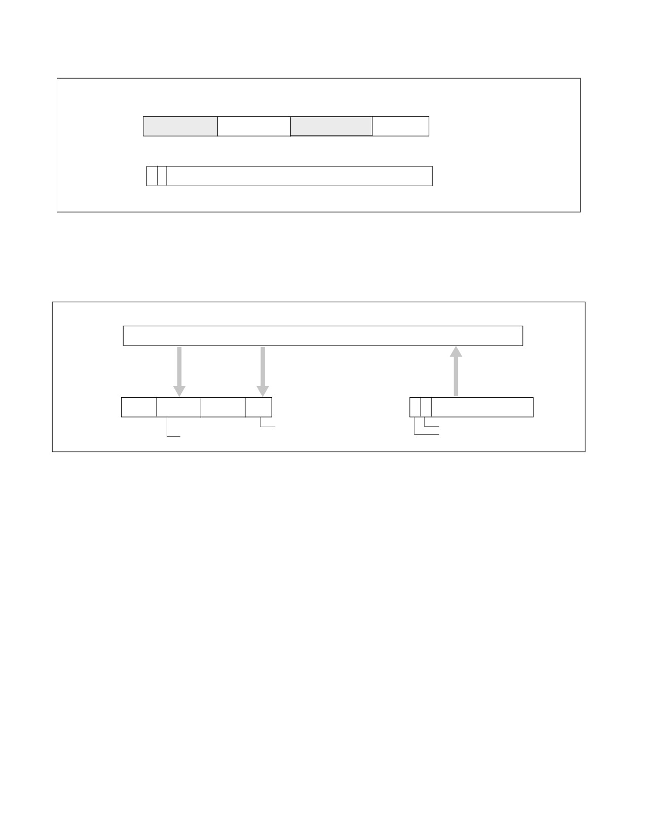
IA32_QM_EVTSEL.EvtID (bits 7:0) specifies an event code of a supported resource type for hardware to report
monitored data associated with IA32_QM_EVTSEL.RMID (bits 41:32). Software can configure
IA32_QM_EVTSEL.RMID with any RMID that is active within the physical processor. The width of
IA32_QM_EVTSEL.RMID matches that of IA32_PQR_ASSOC.RMID. Supported event codes for the
IA32_QM_EVTSEL register are shown in Table 18-18. Note that valid event codes may not necessarily map
directly to the bit position used to enumerate support for the resource via CPUID.
Software can program an RMID / Event ID pair into the IA32_QM_EVTSEL MSR bit field to select an RMID to
read a particular counter for a given resource. The currently supported list of Monitoring Event IDs is discussed
in Section 18.18.5, which covers feature-specific details.
Thread access to the IA32_QM_EVTSEL and IA32_QM_CTR MSR pair should be serialized (that is, treated as a
critical section under lock) to avoid situations where one thread changes the RMID/EvtID just before another
thread reads monitoring data from IA32_QM_CTR.
• IA32_QM_CTR: This MSR reports monitored data when available. It contains three bit fields. If software
configures an unsupported RMID or event type in IA32_QM_EVTSEL, then IA32_QM_CTR.Error (bit 63) will be
set, indicating there is no valid data to report. If IA32_QM_CTR.Unavailable (bit 62) is set, it indicates
monitored data for the RMID is not available, and IA32_QM_CTR.data (bits 61:0) should be ignored. Therefore,
IA32_QM_CTR.data (bits 61:0) is valid only if bit 63 and 62 are both clear. For Cache Monitoring Technology,
software can convert IA32_QM_CTR.data into cache occupancy or bandwidth metrics expressed in bytes by
multiplying with the conversion factor from CPUID.(EAX=0FH, ECX=1H).EBX.
18-50
Vol. 3B
DEBUG, BRANCH PROFILE, TSC, AND INTEL® RESOURCE DIRECTOR TECHNOLOGY (INTEL® RDT) FEATURES
63
4241
32
31
8
7
0
Reserved
RMID
Reserved
EvtID
IA32_QM_EVTSEL
63
61
0
E
U
Resource Monitoring Data
IA32_QM_CTR
Figure 18-24. IA32_QM_EVTSEL and IA32_QM_CTR MSRs
18.18.8 Monitoring Programming Considerations
Figure 18-25 illustrates how system software can program IA32_QOSEVTSEL and IA32_QM_CTR to perform
resource monitoring.
System Software
RMID
Event ID
Counter Data
IA32_QOSEVTSEL MSR
IA32_QM_CTR MSR
63
41
32
7
0
63
62
0
Reserved
RMID
Reserved
EvtID
Monitoring Data
Event ID
Availability
Error
Resource Monitoring ID
Figure 18-25. Software Usage of Cache Monitoring Resources
Though the field provided in IA32_QM_CTR allows for up to 62 bits of data to be returned, often a subset of bits are
used. With Cache Monitoring Technology for instance, the number of bits used is the base-two logarithm of the
total cache size divided by the Upscaling Factor from CPUID.
In Memory Bandwidth Monitoring, the initial counter size is 24 bits, and retrieving the value at 1Hz or faster is suffi-
cient to ensure at most one rollover per sampling period. Any changes to counter width are enumerated to soft-
ware; see Section 18.18.5.2 for details.
18.18.8.1 Monitoring Dynamic Configuration
Both the IA32_QM_EVTSEL and IA32_PQR_ASSOC registers are accessible and modifiable at any time during
execution using RDMSR/WRMSR unless otherwise noted. When writing to these MSRs a #GP(0) will be generated
if any of the following conditions occur:
• A reserved bit is modified,
• An RMID exceeding the maximum RMID is used.
18.18.8.2 Monitoring Operation With Power Saving Features
Some advanced power management features such as deep package C-states may shrink the L3 cache and cause
CMT occupancy count to be reduced. MBM bandwidth counts may increase due to flushing cached data out of L3.
Vol. 3B
18-51
DEBUG, BRANCH PROFILE, TSC, AND INTEL® RESOURCE DIRECTOR TECHNOLOGY (INTEL® RDT) FEATURES
18.18.8.3 Monitoring Operation with Other Operating Modes
The states in IA32_PQR_ASSOC and monitoring counter are unmodified across an SMI delivery. Thus, the execu-
tion of SMM handler code and SMM handler’s data can manifest as spurious contribution in the monitored data.
It is possible for an SMM handler to minimize the impact on of spurious contribution in the QOS monitoring counters
by reserving a dedicated RMID for monitoring the SMM handler. Such an SMM handler can save the previously
configured QOS Monitoring state immediately upon entering SMM, and restoring the QOS monitoring state back to
the prev-SMM RMID upon exit.
18.18.8.4 Monitoring Operation with RAS Features
In general, the Reliability, Availability, and Serviceability (RAS) features present in Intel Platforms are not expected
to significantly affect shared resource monitoring counts. In cases where software RAS features cause memory
copies or cache accesses, these may be tracked and may influence the shared resource monitoring counter values.
18.19 INTEL® RESOURCE DIRECTOR TECHNOLOGY (INTEL® RDT) ALLOCATION
FEATURES
The Intel Resource Director Technology (Intel RDT) feature set provides a set of allocation (resource control) capa-
bilities including Cache Allocation Technology (CAT) and Code and Data Prioritization (CDP). The Intel Xeon
processor E5 v4 family (and a subset of communication-focused processors in the Intel Xeon E5 v3 family) intro-
duce capabilities to configure and make use of the Cache Allocation Technology (CAT) mechanisms on the L3 cache.
Certain Intel Atom processors also provide support for control over the L2 cache, with capabilities as described
below. The programming interface for Cache Allocation Technology and for the more general allocation capabilities
are described in the rest of this chapter. The CAT and CDP capabilities, where architecturally supported, may be
detected and enumerated in software using the CPUID instruction, as described in this chapter.
The Intel Xeon Scalable Processor Family introduces the Memory Bandwidth Allocation (MBA) feature which
provides indirect control over the memory bandwidth available to CPU cores, and is discussed later in this chapter.
18.19.1 Introduction to Cache Allocation Technology (CAT)
Cache Allocation Technology enables an Operating System (OS), Hypervisor /Virtual Machine Manager (VMM) or
similar system service management agent to specify the amount of cache space into which an application can fill
(as a hint to hardware - certain features such as power management may override CAT settings). Specialized user-
level implementations with minimal OS support are also possible, though not necessarily recommended (see notes
below for OS/Hypervisor with respect to ring 3 software and virtual guests). Depending on the processor family, L2
or L3 cache allocation capability may be provided, and the technology is designed to scale across multiple cache
levels and technology generations.
Software can determine which levels are supported in a given platform programmatically using CPUID as described
in the following sections.
The CAT mechanisms defined in this document provide the following key features:
• A mechanism to enumerate platform Cache Allocation Technology capabilities and available resource types that
provides CAT control capabilities. For implementations that support Cache Allocation Technology, CPUID
provides enumeration support to query which levels of the cache hierarchy are supported and specific CAT
capabilities, such as the max allocation bitmask size,
• A mechanism for the OS or Hypervisor to configure the amount of a resource available to a particular Class of
Service via a list of allocation bitmasks,
• Mechanisms for the OS or Hypervisor to signal the Class of Service to which an application belongs, and
• Hardware mechanisms to guide the LLC fill policy when an application has been designated to belong to a
specific Class of Service.
Note that for many usages, an OS or Hypervisor may not want to expose Cache Allocation Technology mechanisms
to Ring3 software or virtualized guests.
18-52
Vol. 3B
DEBUG, BRANCH PROFILE, TSC, AND INTEL® RESOURCE DIRECTOR TECHNOLOGY (INTEL® RDT) FEATURES
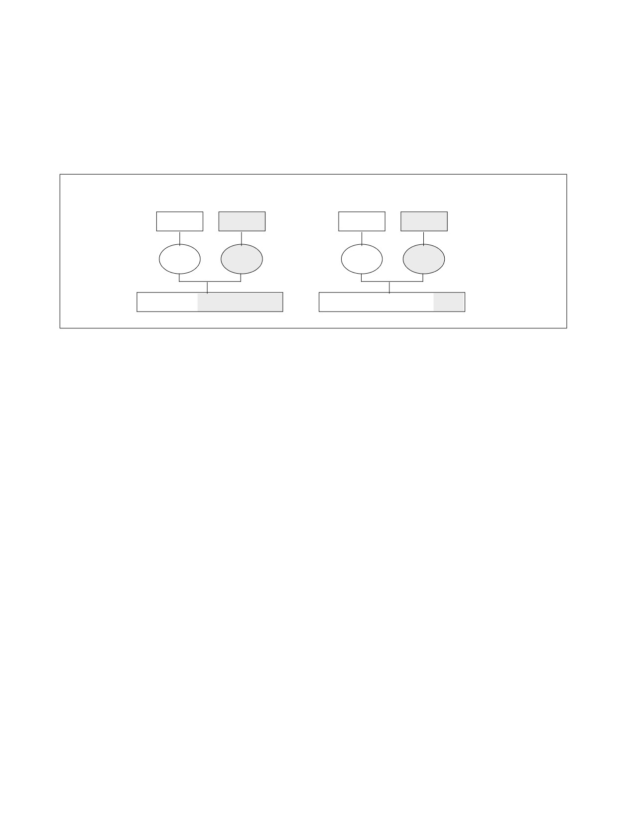
The Cache Allocation Technology feature enables more cache resources (i.e., cache space) to be made available for
high priority applications based on guidance from the execution environment as shown in Figure 18-26. The archi-
tecture also allows dynamic resource reassignment during runtime to further optimize the performance of the high
priority application with minimal degradation to the low priority app. Additionally, resources can be rebalanced for
system throughput benefit across uses cases of OSes, VMMs, containers, and other scenarios by managing the
CPUID and MSR interfaces. This section describes the hardware and software support required in the platform
including what is required of the execution environment (i.e., OS/VMM) to support such resource control. Note that
in Figure 18-26 the L3 Cache is shown as an example resource.
Without CAT
With CAT
Hi Pri App
Lo Pri App
Hi Pri App
Lo Pri App
Core 0
Core 1
Core 0
Core 1
Shared LLC, Low priority got more cache
Shared LLC, High priority got more cache
Figure 18-26. Cache Allocation Technology Enables Allocation of More Resources to High Priority Applications
18.19.2 Cache Allocation Technology Architecture
The fundamental goal of Cache Allocation Technology is to enable resource allocation based on application priority
or Class of Service (COS or CLOS). The processor exposes a set of Classes of Service into which applications (or
individual threads) can be assigned. Cache allocation for the respective applications or threads is then restricted
based on the class with which they are associated. Each Class of Service can be configured using capacity bitmasks
(CBMs) which represent capacity and indicate the degree of overlap and isolation between classes. For each logical
processor there is a register exposed (referred to here as the IA32_PQR_ASSOC MSR or PQR) to allow the OS/VMM
to specify a COS when an application, thread or VM is scheduled.
The usage of Classes of Service (COS) are consistent across resources and a COS may have multiple resource
control attributes attached, which reduces software overhead at context swap time. Rather than adding new types
of COS tags per resource for instance, the COS management overhead is constant. Cache allocation for the indi-
cated application/thread/container/VM is then controlled automatically by the hardware based on the class and the
bitmask associated with that class. Bitmasks are configured via the IA32_resourceType_MASK_n MSRs, where
resourceType indicates a resource type (e.g., “L3” for the L3 cache) and “n” indicates a COS number.
The basic ingredients of Cache Allocation Technology are as follows:
• An architecturally exposed mechanism using CPUID to indicate whether CAT is supported, and what resource
types are available which can be controlled,
• For each available resourceType, CPUID also enumerates the total number of Classes of Services and the length
of the capacity bitmasks that can be used to enforce cache allocation to applications on the platform,
• An architecturally exposed mechanism to allow the execution environment (OS/VMM) to configure the behavior
of different classes of service using the bitmasks available,
• An architecturally exposed mechanism to allow the execution environment (OS/VMM) to assign a COS to an
executing software thread (i.e., associating the active CR3 of a logical processor with the COS in
IA32_PQR_ASSOC),
• Implementation-dependent mechanisms to indicate which COS is associated with a memory access and to
enforce the cache allocation on a per COS basis.
A capacity bitmask (CBM) provides a hint to the hardware indicating the cache space an application should be
limited to as well as providing an indication of overlap and isolation in the CAT-capable cache from other applica-
tions contending for the cache. The bit length of the capacity mask available generally depends on the configura-
Vol. 3B
18-53
DEBUG, BRANCH PROFILE, TSC, AND INTEL® RESOURCE DIRECTOR TECHNOLOGY (INTEL® RDT) FEATURES
tion of the cache and is specified in the enumeration process for CAT in CPUID (this may vary between models in a
processor family as well). Similarly, other parameters such as the number of supported COS may vary for each
resource type, and these details can be enumerated via CPUID.
M7
M6
M5
M4
M3
M2
M1
M0
A
A
A
A
A
A
A
A
COS0
Default Bitmask
COS1
A
A
A
A
A
A
A
A
COS2
A
A
A
A
A
A
A
A
COS3
A
A
A
A
A
A
A
A
M7
M6
M5
M4
M3
M2
M1
M0
A
A
A
A
A
A
A
A
COS0
Overlapped Bitmask
COS1
A
A
A
A
COS2
A
A
COS3
A
M7
M6
M5
M4
M3
M2
M1
M0
COS0
A
A
A
A
Isolated Bitmask
COS1
A
A
COS2
A
COS3
A
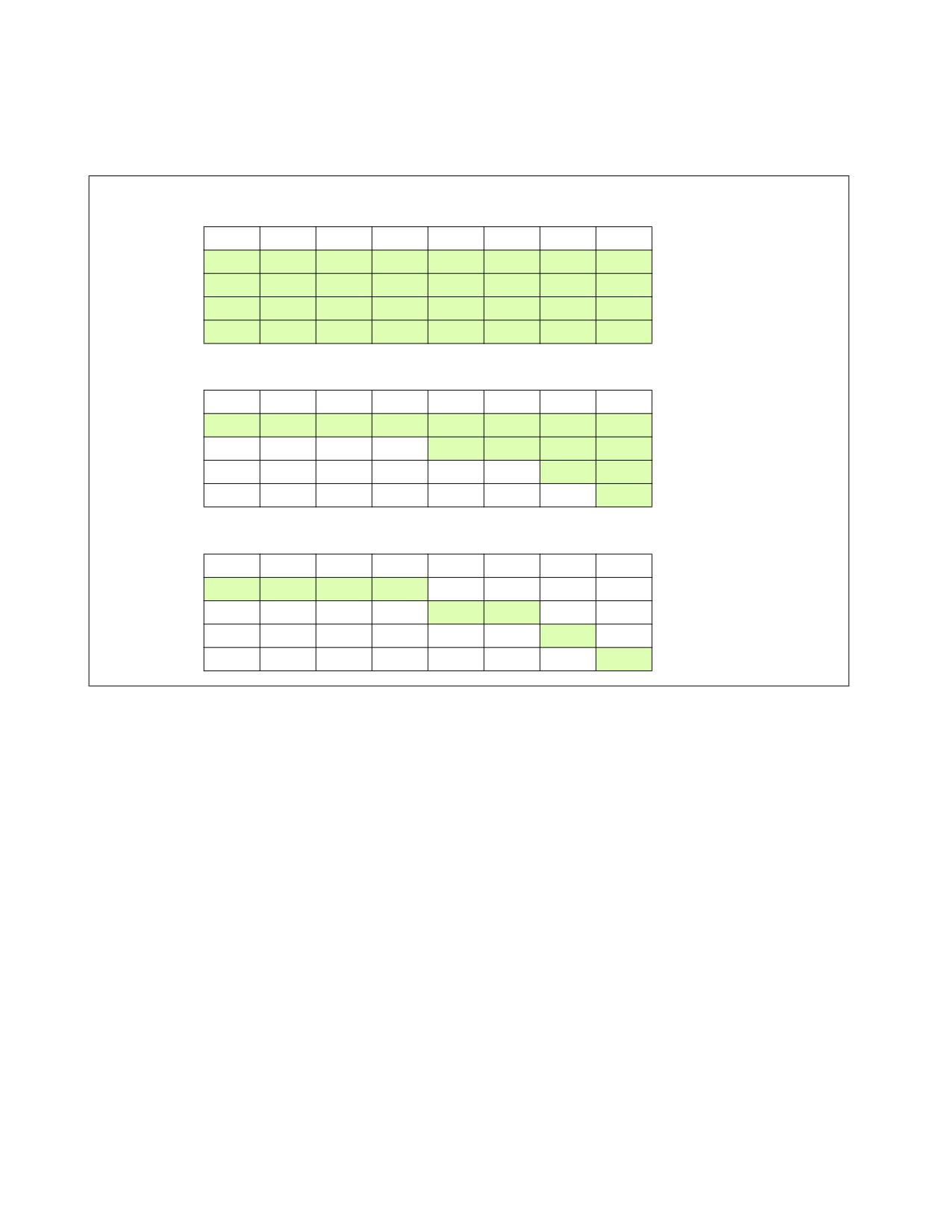
Figure 18-27. Examples of Cache Capacity Bitmasks
Sample cache capacity bitmasks for a bit length of 8 are shown in Figure 18-27. Note that all (and only) contiguous
'1' combinations are allowed (e.g., FFFFH, 0FF0H, 003CH, etc.), unless otherwise non-contiguous capacity bitmask
support is specified in CPUID enumeration for the resource type. Attempts to program a value without contiguous
'1's (including zero) will result in a general protection fault (#GP(0)). It is generally expected that in way-based
implementations, one capacity mask bit corresponds to some number of ways in cache, but the specific mapping is
implementation-dependent. In all cases, a mask bit set to '1' specifies that a particular Class of Service can allocate
into the cache subset represented by that bit. A value of '0' in a mask bit specifies that a Class of Service cannot
allocate into the given cache subset. In general, allocating more cache to a given application is usually beneficial to
its performance.
Figure 18-27 also shows three examples of sets of Cache Capacity Bitmasks. For simplicity these are represented
as 8-bit vectors, though this may vary depending on the implementation and how the mask is mapped to the avail-
able cache capacity. The first example shows the default case where all 4 Classes of Service (the total number of
COS are implementation-dependent) have full access to the cache. The second case shows an overlapped case,
which would allow some lower-priority threads to share cache space with the highest priority threads. The third
case shows various non-overlapped partitioning schemes. As a matter of software policy for extensibility, COS0
should typically be considered and configured as the highest priority COS, followed by COS1, and so on, though
there is no hardware restriction enforcing this mapping. When the system boots all threads are initialized to COS0,
which has full access to the cache by default.
Though the representation of the CBMs looks similar to a way-based mapping they are independent of any specific
enforcement implementation (e.g., way partitioning.) Rather, this is a convenient manner to represent capacity,
overlap, and isolation of cache space. For example, executing a POPCNT instruction (population count of set bits)
18-54
Vol. 3B
DEBUG, BRANCH PROFILE, TSC, AND INTEL® RESOURCE DIRECTOR TECHNOLOGY (INTEL® RDT) FEATURES
on the capacity bitmask can provide the fraction of cache space that a class of service can allocate into. In addition
to the fraction, the exact location of the bits also shows whether the class of service overlaps with other classes of
service or is entirely isolated in terms of cache space used.
Enum/Confg
Association
Enforcement
Enumerate
OS Context
Application
Enforcement
Switch
Memory Request
Configure CBM for
Set Class of Service
Tag with Cache
each Class of Service
in IA32_PQR
Class of Service
Config
COS = 2
Mem Request
COS
Transaction
Cache Subsystem
Enforce Mask
Cache Allocation
Set 1
Set 2
COS 0
Capacity bitmask 3
Set n
COS 1
Capacity bitmask 3
way 1
COS 2
Capacity bitmask 3
COS 3
Capacity bitmask 3
way 16
2
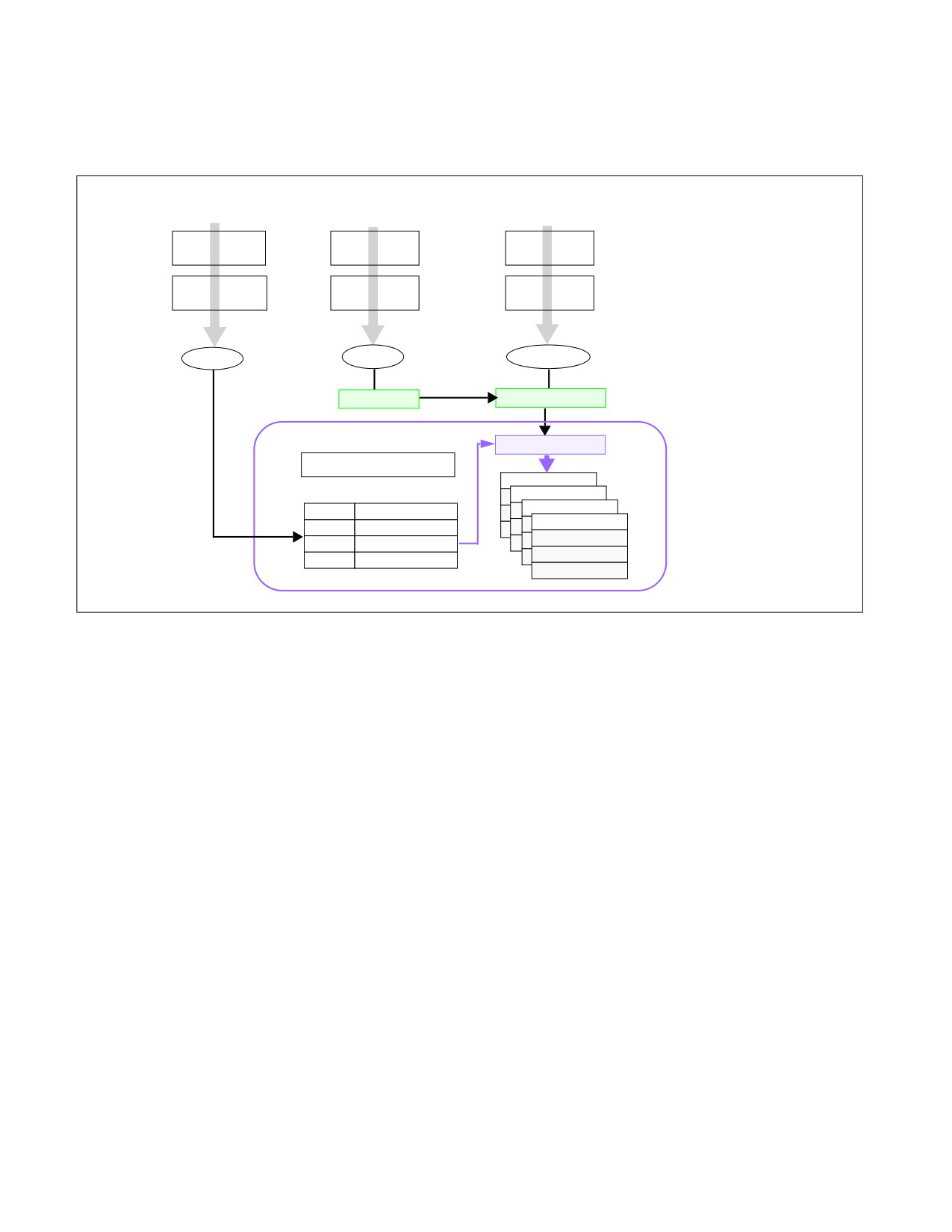
Figure 18-28. Class of Service and Cache Capacity Bitmasks
Figure 18-28 shows how the Cache Capacity Bitmasks and the per-logical-processor Class of Service are logically
used to enable Cache Allocation Technology. All (and only) contiguous 1's in the CBM are permitted, unless other-
wise non-contiguous capacity bitmask support is specified in CPUID enumeration for the resource type. The length
of a CBM may vary from resource to resource or between processor generations and can be enumerated using
CPUID. From the available mask set and based on the goals of the OS/VMM (shared or isolated cache, etc.)
bitmasks are selected and associated with different classes of service. For the available Classes of Service the asso-
ciated CBMs can be programmed via the global set of CAT configuration registers (in the case of L3 CAT, via the
IA32_L3_MASK_n MSRs, where “n” is the Class of Service, starting from zero). In all architectural implementations
supporting CPUID it is possible to change the CBMs dynamically, during program execution, unless stated other-
wise by Intel.
The currently running application's Class of Service is communicated to the hardware through the per-logical-
processor PQR MSR (IA32_PQR_ASSOC MSR). When the OS schedules an application thread on a logical processor,
the application thread is associated with a specific COS (i.e., the corresponding COS in the PQR) and all requests to
the CAT-capable resource from that logical processor are tagged with that COS (in other words, the application
thread is configured to belong to a specific COS). The cache subsystem uses this tagged request information to
enforce QoS. The capacity bitmask may be mapped into a way bitmask (or a similar enforcement entity based on
the implementation) at the cache before it is applied to the allocation policy. For example, the capacity bitmask can
be an 8-bit mask and the enforcement may be accomplished using a 16-way bitmask for a cache enforcement
implementation based on way partitioning.
The following sections describe extensions of CAT such as Code and Data Prioritization (CDP), followed by details
on specific features such as L3 CAT, L3 CDP, L2 CAT, and L2 CDP. Depending on the specific processor a mix of
features may be supported, and CPUID provides enumeration capabilities to enable software to dynamically detect
the set of supported features.
Vol. 3B
18-55

DEBUG, BRANCH PROFILE, TSC, AND INTEL® RESOURCE DIRECTOR TECHNOLOGY (INTEL® RDT) FEATURES
18.19.3 Code and Data Prioritization (CDP) Technology
Code and Data Prioritization Technology is an extension of CAT. CDP enables isolation and separate prioritization of
code and data fetches to the L2 or L3 cache in a software configurable manner, depending on hardware support,
which can enable workload prioritization and tuning of cache capacity to the characteristics of the workload. CDP
extends Cache Allocation Technology (CAT) by providing separate code and data masks per Class of Service (COS).
Support for the L2 CDP feature and the L3 CDP features are separately enumerated (via CPUID) and separately
controlled (via remapping the L2 CAT MSRs or L3 CAT MSRs respectively). Section 18.19.6.3 and Section 18.19.7
provide details on enumerating, controlling, and enabling L3 and L2 CDP respectively, while this section provides a
general overview.
The L3 CDP feature was first introduced on the Intel Xeon E5 v4 family of server processors, as an extension to L3
CAT. The L2 CDP feature is first introduced on future Intel Atom family processors, as an extension to L2 CAT.
By default, CDP is disabled on the processor. If the CAT MSRs are used without enabling CDP, the processor oper-
ates in a traditional CAT-only mode. When CDP is enabled,
• the CAT mask MSRs are re-mapped into interleaved pairs of mask MSRs for data or code fetches (see
Figure 18-29),
• the range of COS for CAT is re-indexed, with the lower-half of the COS range available for CDP.
Using the CDP feature, virtual isolation between code and data can be configured on the L2 or L3 cache if desired,
similar to how some processor cache levels provide separate L1 data and L1 instruction caches.
Like the CAT feature, CDP may be dynamically configured by privileged software at any point during normal system
operation, including dynamically enabling or disabling the feature provided that certain software configuration
requirements are met (see Section 18.19.5).
An example of the operating mode of CDP is shown in Figure 18-29. Shown at the top are traditional CAT usage
models where capacity masks map 1:1 with a COS number to enable control over the cache space which a given
COS (and thus applications, threads or VMs) may occupy. Shown at the bottom are example mask configurations
where CDP is enabled, and each COS number maps 1:2 to two masks, one for code and one for data. This enables
code and data to be either overlapped or isolated to varying degrees either globally or on a per-COS basis,
depending on application and system needs.
Example of CAT-Only Usage - 16 bit Capacity Masks
COS0
1
1
1
1
0
0
0
0
0
0
0
0
0
0
0
0
COS1
0
0
0
0
1
1
1
1
0
0
0
0
0
0
0
0
Traditional
COS2
0
0
0
0
0
0
0
0
1
1
0
0
0
0
0
0
CAT
COS3
0
0
0
0
0
0
0
0
1
1
1
1
1
1
1
1
Example of Code/Data Prioritization Usage - 16 bit Capacity Masks
1
1
1
1
0
0
0
0
0
0
0
0
0
0
0
0
COS0.Data
0
0
0
0
1
1
0
0
0
0
0
0
0
0
0
0
COS0.Code
CAT with
0
0
0
0
0
0
1
1
1
1
1
0
0
0
0
0
CDP
COS1.Data
0
0
0
0
0
0
0
0
0
1
1
1
0
0
0
0
COS1.Code
0
0
0
0
0
0
0
0
0
0
0
0
1
1
1
1
Other COS.Data
Other COS.Code
0
0
0
0
0
0
0
0
0
0
0
0
1
1
1
1
Figure 18-29. Code and Data Capacity Bitmasks of CDP
18-56
Vol. 3B

DEBUG, BRANCH PROFILE, TSC, AND INTEL® RESOURCE DIRECTOR TECHNOLOGY (INTEL® RDT) FEATURES
When CDP is enabled, the existing mask space for CAT-only operation is split. As an example if the system supports
16 CAT-only COS, when CDP is enabled the same MSR interfaces are used, however half of the masks correspond
to code, half correspond to data, and the effective number of COS is reduced by half. Code/Data masks are defined
per-COS and interleaved in the MSR space as described in subsequent sections.
In cases where CPUID exposes a non-even number of supported Classes of Service for the CAT or CDP features,
software using CDP should use the lower matched pairs of code/data masks, and any upper unpaired masks should
not be used. As an example, if CPUID exposes 5 CLOS, when CDP is enabled then two code/data pairs are available
(masks 0/1 for CLOS[0] data/code and masks 2/3 for CLOS[1] data/code), however the upper un-paired mask
should not be used (mask 4 in this case) or undefined behavior may result.
18.19.4 Enabling Cache Allocation Technology Usage Flow
Figure 18-30 illustrates the key steps for OS/VMM to detect support of Cache Allocation Technology and enable
priority-based resource allocation for a CAT-capable resource.
On OS/VMM Initialization
Cache Allocation Configuration
On Context Switch
CQE Capability
Configure CBM
Set COS for scheduled
Enumeration
per COS
thread context
CPUID[
WRMSR
WRMSR
CPUID.(7,0):EBX.15
IA32_L3_QOS_MASK_0
CPUID.(10H,0):EBX[31:1]
IA32_PQR_ASSOC
CPUID.(10H,1):EAX[4:0]
CPUID.(10H,1):EDX[15:0]
IA32_L3_QOS_MASK_n
CPUID.(10H,1):EBX[
Figure 18-30. Cache Allocation Technology Usage Flow
Enumeration and configuration of L2 CAT is similar to L3 CAT, however CPUID details and MSR addresses differ.
Common CLOS are used across the features.
18.19.4.1 Enumeration and Detection Support of Cache Allocation Technology
Software can query processor support of CAT capabilities by executing CPUID instruction with EAX = 07H, ECX =
0H as input. If CPUID.(EAX=07H, ECX=0):EBX.PQE[bit 15] reports 1, the processor supports software control over
shared processor resources. Software must use CPUID leaf 10H to enumerate additional details of available
resource types, classes of services and capability bitmasks. The programming interfaces provided by Cache Alloca-
tion Technology include:
• CPUID leaf function 10H (Cache Allocation Technology Enumeration leaf) and its sub-functions provide
information on available resource types, and CAT capability for each resource type (see Section 18.19.4.2).
• IA32_L3_MASK_n: A range of MSRs is provided for each resource type, each MSR within that range specifying
a software-configured capacity bitmask for each class of service. For L3 with Cache Allocation support, the CBM
is specified using one of the IA32_L3_QOS_MASK_n MSR, where 'n' corresponds to a number within the
supported range of COS, i.e., the range between 0 and CPUID.(EAX=10H, ECX=ResID):EDX[15:0], inclusive.
See Section 18.19.4.3 for details.
• IA32_L2_MASK_n: A range of MSRs is provided for L2 Cache Allocation Technology, enabling software control
over the amount of L2 cache available for each CLOS. Similar to L3 CAT, a CBM is specified for each CLOS using
the set of registers, IA32_L2_QOS_MASK_n MSR, where 'n' ranges from zero to the maximum CLOS number
reported for L2 CAT in CPUID. See Section 18.19.4.3 for details.
The L2 mask MSRs are scoped at the same level as the L2 cache (similarly, the L3 mask MSRs are scoped at the
same level as the L3 cache). Software may determine which logical processors share an MSR (for instance local
Vol. 3B
18-57

DEBUG, BRANCH PROFILE, TSC, AND INTEL® RESOURCE DIRECTOR TECHNOLOGY (INTEL® RDT) FEATURES
to a core, or shared across multiple cores) by performing a write to one of these MSRs and noting which logical
threads observe the change. Example flows for a similar method to determine register scope are described in
Section 16.5.2, “System Software Recommendation for Managing CMCI and Machine Check Resources.”
Software may also use CPUID leaf 4 to determine the maximum number of logical processor IDs that may share
a given level of the cache.
• IA32_PQR_ASSOC.CLOS: The IA32_PQR_ASSOC MSR provides a COS field that OS/VMM can use to assign a
logical processor to an available COS. The set of COS are common across all allocation features, meaning that
multiple features may be supported in the same processor without additional software COS management
overhead at context swap time. See Section 18.19.4.4 for details.
18.19.4.2 Cache Allocation Technology: Resource Type and Capability Enumeration
CPUID leaf function 10H (Cache Allocation Technology Enumeration leaf) provides two or more sub-functions:
• CAT Enumeration leaf sub-function 0 enumerates available resource types that support allocation control, i.e.,
by executing CPUID with EAX=10H and ECX=0H. Each supported resource type is represented by a bit field in
CPUID.(EAX=10H, ECX=0):EBX[31:1]. The bit position of each set bit corresponds to a Resource ID (ResID),
for instance ResID=1 is used to indicate L3 CAT support, and ResID=2 indicates L2 CAT support. The ResID is
also the sub-leaf index that software must use to query details of the CAT capability of that resource type (see
Figure 18-31).
CPUID.(EAX=10H, ECX=0) Output: (EAX: Reserved; ECX: Reserved; EDX: Reserved)
31
4
3
2
1
0
M
L
L
EBX
Reserved
B
2
3
A
Figure 18-31. CPUID.(EAX=10H, ECX=0H) Available Resource Type Identification
— For ECX>0, EAX[4:0] reports the length of the capacity bitmask (ECX=1 or 2 for L3 CAT or L2 CAT respec-
tively). Add one to the return value to get the result, e.g., a value of 15 corresponds to the capacity bitmask
having length of 16 bits. Bits 31:5 of EAX are reserved.
• Sub-functions of CPUID.EAX=10H with a non-zero ECX input matching a supported ResID enumerate the
specific enforcement details of the corresponding ResID. The capabilities enumerated include the length of the
capacity bitmasks and the number of Classes of Service for a given ResID. Software should query the capability
of each available ResID that supports CAT from a sub-leaf of leaf 10H using the sub-leaf index reported by the
corresponding non-zero bit in CPUID.(EAX=10H, ECX=0):EBX[31:1] in order to obtain additional feature
details.
18-58
Vol. 3B

DEBUG, BRANCH PROFILE, TSC, AND INTEL® RESOURCE DIRECTOR TECHNOLOGY (INTEL® RDT) FEATURES
CPUID.(EAX=10H, ECX=ResID=1) Output:
31
5
4
0
EAX
Reserved
CBM_LEN
31
0
EBX
Bitmask of Shareable Resource with Other Executing Entities
31
3
2
1
0
ECX
Reserved
L3 CAT for Non-CPU
Agents
CDP
Non-contiguous
Capacity Bitmask
31
16
15
0
EDX
Reserved
COS_MAX
Figure 18-32. L3 Cache Allocation Technology and CDP Enumeration
•
CAT capability for L3 is enumerated by CPUID.(EAX=10H, ECX=1H), see Figure 18-32. The specific CAT
capabilities reported by CPUID.(EAX=10H, ECX=1) are:
— CPUID.(EAX=10H, ECX=ResID=1):EAX[4:0] reports the length of the capacity bitmask. Add one to the
return value to get the result, e.g., a value of 15 corresponds to the capability bitmask having length of 16
bits. Bits 31:5 of EAX are reserved.
— CPUID.(EAX=10H, ECX=1):EBX[31:0] reports a bit mask. Each set bit within the length of the CBM
indicates the corresponding unit of the L3 allocation may be used by other entities in the platform (e.g., an
integrated graphics engine or hardware units outside the processor core and have direct access to L3). Each
cleared bit within the length of the CBM indicates the corresponding allocation unit can be configured to
implement a priority-based allocation scheme chosen by an OS/VMM without interference with other
hardware agents in the system. Bits outside the length of the CBM are reserved.
— CPUID.(EAX=10H, ECX=1):ECX[bit 1]: If 1, indicates L3 CAT for non-CPU agents is supported. Bits 0 and
31:4 of ECX are reserved. See section 18.20 for details.
— CPUID.(EAX=10H, ECX=1):ECX.CDP[bit 2]: If 1, indicates L3 Code and Data Prioritization Technology is
supported (see Section 18.19.5). Bits 0 and 31:4 of ECX are reserved.
— CPUID.(EAX=10H, ECX=1):ECX[bit 3]: If 1, indicates non-contiguous capacity bitmask is supported. The
bits that are set in the various IA32_L3_MASK_n registers do not have to be contiguous. Bits 0 and 31:4 of
ECX are reserved.
— CPUID.(EAX=10H, ECX=1):EDX[15:0] reports the maximum COS supported for the resource (COS are
zero-referenced, meaning a reported value of '15' would indicate 16 total supported COS). Bits 31:16 are
reserved.
Vol. 3B
18-59

DEBUG, BRANCH PROFILE, TSC, AND INTEL® RESOURCE DIRECTOR TECHNOLOGY (INTEL® RDT) FEATURES
CPUID.(EAX=10H, ECX=ResID=2) Output:
31
5
4
0
EAX
Reserved
CBM_LEN
31
0
EBX
Bitmask of Shareable Resource with Other Executing Entities
31
3
2
1
0
ECX
Reserved
CDP
Non-Contiguous
Capacity Bitmask
31
16
15
0
EDX
Reserved
COS_MAX
Figure 18-33. L2 Cache Allocation Technology
•
CAT capability for L2 is enumerated by CPUID.(EAX=10H, ECX=2H), see Figure 18-33. The specific CAT
capabilities reported by CPUID.(EAX=10H, ECX=2) are:
— CPUID.(EAX=10H, ECX=ResID=2):EAX[4:0] reports the length of the capacity bitmask. Add one to the
return value to get the result, e.g., a value of 15 corresponds to the capability bitmask having length of 16
bits. Bits 31:5 of EAX are reserved.
— CPUID.(EAX=10H, ECX=2):EBX[31:0] reports a bit mask. Each set bit within the length of the CBM
indicates the corresponding unit of the L2 allocation may be used by other entities in the platform. Each
cleared bit within the length of the CBM indicates the corresponding allocation unit can be configured to
implement a priority-based allocation scheme chosen by an OS/VMM without interference with other
hardware agents in the system. Bits outside the length of the CBM are reserved.
— CPUID.(EAX=10H, ECX=2):ECX.CDP[bit 2]: If 1, indicates L2 Code and Data Prioritization Technology is
supported (see Section 17.19.6). Bits 1:0 and 31:4 of ECX are reserved.
— CPUID.(EAX=10H, ECX=2):ECX[bit 3]: If 1, indicates non-contiguous capacity bitmask is supported. The
bits which are set in the various IA32_L2_MASK_n registers do not have to be contiguous. Bits 1:0 and 31:4
of ECX are reserved.
— CPUID.(EAX=10H, ECX=2):EDX[15:0] reports the maximum COS supported for the resource (COS are
zero-referenced, meaning a reported value of '15' would indicate 16 total supported COS). Bits 31:16 are
reserved.
A note on migration of Classes of Service (COS): Software should minimize migrations of COS across logical
processors (across threads or cores), as a reduction in the performance of the Cache Allocation Technology feature
may result if COS are migrated frequently. This is aligned with the industry-standard practice of minimizing unnec-
essary thread migrations across processor cores in order to avoid excessive time spent warming up processor
caches after a migration. In general, for best performance, minimize thread migration and COS migration across
processor logical threads and processor cores.
18-60
Vol. 3B

DEBUG, BRANCH PROFILE, TSC, AND INTEL® RESOURCE DIRECTOR TECHNOLOGY (INTEL® RDT) FEATURES
18.19.4.3 Cache Allocation Technology: Cache Mask Configuration
After determining the length of the capacity bitmasks (CBM) and number of COS supported using CPUID (see
Section 18.19.4.2), each COS needs to be programmed with a CBM to dictate its available cache via a write to the
corresponding IA32_resourceType_MASK_n register, where 'n' corresponds to a number within the supported
range of COS, i.e., the range between 0 and CPUID.(EAX=10H, ECX=ResID):EDX[15:0], inclusive, and 'resource-
Type' corresponds to a specific resource as enumerated by the set bits of CPUID.(EAX=10H, ECX=0):EBX[31:1],
for instance, ‘L2’ or ‘L3’ cache.
A hierarchy of MSRs is reserved for Cache Allocation Technology registers of the form IA32_resource-
Type_MASK_n:
• From 0C90H through 0D8FH (inclusive), providing support for multiple sub-ranges to support varying resource
types. The first supported resource type is 'L3', corresponding to the L3 cache in a platform. The MSRs range
from 0C90H through 0D0FH (inclusive), enables support for up to 128 L3 CAT Classes of Service.
63
31
10
9
0
COS
Reserved
RMID
IA32_PQR_ASSOC
63
32
31
0
Reserved
Bit_Mask
IA32_L3_MASK_0
63
32
31
0
Reserved
Bit_Mask
IA32_L3_MASK_n
Figure 18-34. IA32_PQR_ASSOC, IA32_L3_MASK_n MSRs
• Within the same CAT range hierarchy, another set of registers is defined for resourceType 'L2', corresponding
to the L2 cache in a platform, and MSRs IA32_L2_MASK_n are defined for n=[0,63] at addresses 0D10H
through 0D4FH (inclusive).
Figure 18-34 and Figure 18-35 provide an overview of the relevant registers.
63
32
31
0
Reserved
Bit_Mask
IA32_L2_MASK_0
63
32
31
0
Reserved
Bit_Mask
IA32_L2_MASK_n
Figure 18-35. IA32_L2_MASK_n MSRs
All CAT configuration registers can be accessed using the standard RDMSR / WRMSR instructions.
Note that once L3 or L2 CAT masks are configured, threads can be grouped into Classes of Service (COS) using the
IA32_PQR_ASSOC MSR as described in Section 18.19.4.4, “Class of Service to Cache Mask Association: Common
Across Allocation Features.”
18.19.4.4 Class of Service to Cache Mask Association: Common Across Allocation Features
After configuring the available classes of service with the preferred set of capacity bitmasks, the OS/VMM can set
the IA32_PQR_ASSOC.COS of a logical processor to the class of service with the desired CBM when a thread
Vol. 3B
18-61

DEBUG, BRANCH PROFILE, TSC, AND INTEL® RESOURCE DIRECTOR TECHNOLOGY (INTEL® RDT) FEATURES
context switch occurs. This allows the OS/VMM to indicate which class of service an executing thread/VM belongs
within. Each logical processor contains an instance of the IA32_PQR_ASSOC register at MSR location 0C8FH, and
Figure 18-34 shows the bit field layout for this register. Bits[63:32] contain the COS field for each logical processor.
Note that placing the RMID field within the same PQR register enables both RMID and CLOS to be swapped at
context swap time for simultaneous use of monitoring and allocation features with a single register write for effi-
ciency.
When CDP is enabled, Specifying a COS value in IA32_PQR_ASSOC.COS greater than MAX_COS_CDP =
(CPUID.(EAX=10H, ECX=1):EDX[15:0] >> 1) will cause undefined performance impact to code and data fetches.
In all cases, code and data masks for L2 and L3 CDP should be programmed with at least one bit set.
Note that if the IA32_PQR_ASSOC.COS is never written then the CAT capability defaults to using COS 0, which in
turn is set to the default mask in IA32_L3_MASK_0 - which is all “1”s (on reset). This essentially disables the
enforcement feature by default or for legacy operating systems and software.
See Section 18.19.7, “Introduction to Memory Bandwidth Allocation,” for important COS programming consider-
ations including maximum values when using CAT and CDP.
18.19.5 Code and Data Prioritization (CDP): Enumerating and Enabling L3 CDP Technology
L3 CDP is an extension of L3 CAT. The presence of the L3 CDP feature is enumerated via CPUID.(EAX=10H,
ECX=1):ECX.CDP[bit 2] (see Figure 18-32). Most of the CPUID.(EAX=10H, ECX=1) sub-leaf data that applies to
CAT also apply to CDP. However, CPUID.(EAX=10H, ECX=1):EDX.COS_MAX_CAT specifies the maximum COS
applicable to CAT-only operation. For CDP operations, COS_MAX_CDP is equal to (CPUID.(EAX=10H,
ECX=1):EDX.COS_MAX_CAT >>1).
If CPUID.(EAX=10H, ECX=1):ECX.CDP[bit 2] =1, the processor supports CDP and provides a new MSR
IA32_L3_QOS_CFG at address 0C81H. The layout of IA32_L3_QOS_CFG is shown in Figure 18-36. The bit field
definition of IA32_L3_QOS_CFG are:
• Bit 0: L3 CDP Enable. If set, enables CDP, maps CAT mask MSRs into pairs of Data Mask and Code Mask MSRs.
The maximum allowed value to write into IA32_PQR_ASSOC.COS is COS_MAX_CDP.
• Bits 63:1: Reserved. Attempts to write to reserved bits result in a #GP(0).
IA32_L3_QOS_CFG
63
3
2 1
0
Reserved
L3 CDP Enable
Figure 18-36. Layout of IA32_L3_QOS_CFG
IA32_L3_QOS_CFG default values are all 0s at RESET, the mask MSRs are all 1s. Hence, all logical processors are
initialized in COS0 allocated with the entire L3 with CDP disabled, until software programs CAT and CDP. The scope
of the IA32_L3_QOS_CFG MSR is defined to be the same scope as the L3 cache (e.g., typically per processor
socket). Refer to Section 18.19.7 for software considerations while enabling or disabling L3 CDP.
18.19.5.1 Mapping Between L3 CDP Masks and CAT Masks
When CDP is enabled, the existing CAT mask MSR space is re-mapped to provide a code mask and a data mask per
COS. The re-mapping is shown in Table 18-19.
18-62
Vol. 3B

DEBUG, BRANCH PROFILE, TSC, AND INTEL® RESOURCE DIRECTOR TECHNOLOGY (INTEL® RDT) FEATURES
Table 18-19. Re-indexing of COS Numbers and Mapping to CAT/CDP Mask MSRs
Mask MSR
CAT-only Operation
CDP Operation
IA32_L3_QOS_Mask_0
COS0
COS0.Data
IA32_L3_QOS_Mask_1
COS1
COS0.Code
IA32_L3_QOS_Mask_2
COS2
COS1.Data
IA32_L3_QOS_Mask_3
COS3
COS1.Code
IA32_L3_QOS_Mask_4
COS4
COS2.Data
IA32_L3_QOS_Mask_5
COS5
COS2.Code
IA32_L3_QOS_Mask_’2n’
COS’2n’
COS’n’.Data
IA32_L3_QOS_Mask_’2n+1’
COS’2n+1’
COS’n’.Code
One can derive the MSR address for the data mask or code mask for a given COS number ‘n’ by:
• data_mask_address (n) = base + (n <<1), where base is the address of IA32_L3_QOS_MASK_0.
• code_mask_address (n) = base + (n <<1) +1.
When CDP is enabled, each COS is mapped 1:2 with mask MSRs, with one mask enabling programmatic control
over data fill location and one mask enabling control over code placement. A variety of overlapped and isolated
mask configurations are possible (see the example in Figure 18-29).
Mask MSR field definitions remain the same. Capacity masks must be formed of contiguous set bits, unless other-
wise non-contiguous capacity bitmask support is specified in CPUID enumeration for the resource type with a
length of 1 bit or longer and should not exceed the maximum mask length specified in CPUID. As examples, valid
masks on a cache with max bitmask length of 16b (from CPUID) include 0xFFFF, 0xFF00, 0x00FF, 0x00F0, 0x0001,
0x0003, and so on. Maximum valid mask lengths are unchanged whether CDP is enabled or disabled, and writes of
invalid mask values may lead to undefined behavior. Writes to reserved bits will generate #GP(0).
18.19.6 Code and Data Prioritization (CDP): Enumerating and Enabling L2 CDP Technology
L2 CDP is an extension of the L2 CAT feature. The presence of the L2 CDP feature is enumerated via
CPUID.(EAX=10H, ECX=2):ECX.CDP[bit 2] (see Figure 17-33). Most of the CPUID.(EAX=10H, ECX=2) sub-leaf
data that applies to CAT also apply to CDP. However, CPUID.(EAX=10H, ECX=2):EDX.COS_MAX_CAT specifies the
maximum COS applicable to CAT-only operation. For CDP operations, COS_MAX_CDP is equal to
(CPUID.(EAX=10H, ECX=2):EDX.COS_MAX_CAT >>1).
If CPUID.(EAX=10H, ECX=2):ECX.CDP[bit 2] =1, the processor supports L2 CDP and provides a new MSR
IA32_L2_QOS_CFG at address 0C82H. The layout of IA32_L2_QOS_CFG is shown in Figure 18-37. The bit field
definition of IA32_L2_QOS_CFG are:
• Bit 0: L2 CDP Enable. If set, enables CDP, maps CAT mask MSRs into pairs of Data Mask and Code Mask MSRs.
The maximum allowed value to write into IA32_PQR_ASSOC.COS is COS_MAX_CDP.
• Bits 63:1: Reserved. Attempts to write to reserved bits result in a #GP(0).
IA32_L2_QOS_CFG
63
3
2 1
0
Reserved
L2 CDP Enable
Figure 18-37. Layout of IA32_L2_QOS_CFG
Vol. 3B
18-63
DEBUG, BRANCH PROFILE, TSC, AND INTEL® RESOURCE DIRECTOR TECHNOLOGY (INTEL® RDT) FEATURES
IA32_L2_QOS_CFG default values are all 0s at RESET, and the mask MSRs are all 1s. Hence all logical processors
are initialized in COS0 allocated with the entire L2 available and with CDP disabled, until software programs CAT
and CDP. The IA32_L2_QOS_CFG MSR is defined at the same scope as the L2 cache, typically at the module level
for Intel Atom processors for instance. In processors with multiple modules present it is recommended to program
the IA32_L2_QOS_CFG MSR consistently across all modules for simplicity.
18.19.6.1 Mapping Between L2 CDP Masks and L2 CAT Masks
When CDP is enabled, the existing CAT mask MSR space is re-mapped to provide a code mask and a data mask per
COS. This remapping is the same as the remapping shown in Table 18-19 for L3 CDP, but for the L2 MSR block
(IA32_L2_QOS_MASK_n) instead of the L3 MSR block (IA32_L3_QOS_MASK_n). The same code / data mask
mapping algorithm applies to remapping the MSR block between code and data masks.
As with L3 CDP, when L2 CDP is enabled, each COS is mapped 1:2 with mask MSRs, with one mask enabling
programmatic control over data fill location and one mask enabling control over code placement. A variety of over-
lapped and isolated mask configurations are possible (see the example in Figure 18-29).
Mask MSR field definitions for L2 CDP remain the same as for L2 CAT. Capacity masks must be formed of contiguous
set bits, unless otherwise non-contiguous capacity bitmask support is specified in CPUID enumeration for the
resource type with a length of 1 bit or longer and should not exceed the maximum mask length specified in CPUID.
As examples, valid masks on a cache with max bitmask length of 16b (from CPUID) include 0xFFFF, 0xFF00,
0x00FF, 0x00F0, 0x0001, 0x0003, and so on. Maximum valid mask lengths are unchanged whether CDP is enabled
or disabled, and writes of invalid mask values may lead to undefined behavior. Writes to reserved bits will generate
#GP(0).
18.19.6.2 Common L2 and L3 CDP Programming Considerations
Before enabling or disabling L2 or L3 CDP, software should write all 1's to all of the corresponding CAT/CDP masks
to ensure proper behavior (e.g., the IA32_L3_QOS_Mask_n set of MSRs for the L3 CAT feature). When enabling
CDP, software should also ensure that only COS number which are valid in CDP operation is used, otherwise unde-
fined behavior may result. For instance in a case with 16 CAT COS, since COS are reduced by half when CDP is
enabled, software should ensure that only COS 0-7 are in use before enabling CDP (along with writing 1's to all
mask bits before enabling or disabling CDP).
Software should also account for the fact that mask interpretations change when CDP is enabled or disabled,
meaning for instance that a CAT mask for a given COS may become a code mask for a different Class of Service
when CDP is enabled. In order to simplify this behavior and prevent unintended remapping software should
consider resetting all threads to COS[0] before enabling or disabling CDP.
18.19.6.3 Cache Allocation Technology Dynamic Configuration
All Intel Resource Director Technology (Intel RDT) interfaces including the IA32_PQR_ASSOC MSR, CAT/CDP
masks, MBA delay values, and CQM/MBM registers are accessible and modifiable at any time during execution
using RDMSR/WRMSR unless otherwise noted. When writing to these MSRs a #GP(0) will be generated if any of the
following conditions occur:
• A reserved bit is modified,
• Accessing a QOS mask register outside the supported COS (the max COS number is specified in
CPUID.(EAX=10H, ECX=ResID):EDX[15:0]), or
• Writing a COS greater than the supported maximum (specified as the maximum value of CPUID.(EAX=10H,
ECX=ResID):EDX[15:0] for all valid ResID values) is written to the IA32_PQR_ASSOC.CLOS field.
When CDP is enabled, specifying a COS value in IA32_PQR_ASSOC.COS outside of the lower half of the COS space
will cause undefined performance impact to code and data fetches due to MSR space re-indexing into code/data
masks when CDP is enabled.
When reading the IA32_PQR_ASSOC register the currently programmed COS on the core will be returned.
When reading an IA32_resourceType_MASK_n register the current capacity bit mask for COS 'n' will be returned.
18-64
Vol. 3B
DEBUG, BRANCH PROFILE, TSC, AND INTEL® RESOURCE DIRECTOR TECHNOLOGY (INTEL® RDT) FEATURES
As noted previously, software should minimize migrations of COS across logical processors (across threads or
cores), as a reduction in the accuracy of the Cache Allocation feature may result if COS are migrated frequently.
This is aligned with the industry standard practice of minimizing unnecessary thread migrations across processor
cores in order to avoid excessive time spent warming up processor caches after a migration. In general, for best
performance, minimize thread migration and COS migration across processor logical threads and processor cores.
18.19.6.4 Cache Allocation Technology Operation With Power Saving Features
Note that the Cache Allocation Technology feature cannot be used to enforce cache coherency, and that some
advanced power management features such as C-states which may shrink or power off various caches within the
system may interfere with CAT hints - in such cases the CAT bitmasks are ignored and the other features take
precedence. If the highest possible level of CAT differentiation or determinism is required, disable any power-
saving features which shrink the caches or power off caches. The details of the power management interfaces are
typically implementation-specific, but can be found at Intel® 64 and IA-32 Architectures Software Developer’s
Manual, Volume 3C.
If software requires differentiation between threads but not absolute determinism then in many cases it is possible
to leave power-saving cache shrink features enabled, which can provide substantial power savings and increase
battery life in mobile platforms. In such cases when the caches are powered off (e.g., package C-states) the entire
cache of a portion thereof may be powered off. Upon resuming an active state any new incoming data to the cache
will be filled subject to the cache capacity bitmasks. Any data in the cache prior to the cache shrink or power off
may have been flushed to memory during the process of entering the idle state, however, and is not guaranteed to
remain in the cache. If differentiation between threads is the goal of system software then this model allows
substantial power savings while continuing to deliver performance differentiation. If system software needs
optimal determinism then power saving modes which flush portions of the caches and power them off should be
disabled.
NOTE
IA32_PQR_ASSOC is saved and restored across C6 entry/exit. Similarly, the mask register contents
are saved across package C-state entry/exit and are not lost.
18.19.6.5 Cache Allocation Technology Operation with Other Operating Modes
The states in IA32_PQR_ASSOC and mask registers are unmodified across an SMI delivery. Thus, the execution of
SMM handler code can interact with the Cache Allocation Technology resource and manifest some degree of non-
determinism to the non-SMM software stack. An SMM handler may also perform certain system-level or power
management practices that affect CAT operation.
It is possible for an SMM handler to minimize the impact on data determinism in the cache by reserving a COS with
a dedicated partition in the cache. Such an SMM handler can switch to the dedicated COS immediately upon
entering SMM, and switching back to the previously running COS upon exit.
18.19.6.6 Associating Threads with CAT/CDP Classes of Service
Threads are associated with Classes of Service (CLOS) via the per-logical-processor IA32_PQR_ASSOC MSR. The
same COS concept applies to both CAT and CDP (for instance, COS[5] means the same thing whether CAT or CDP
is in use, and the COS has associated resource usage constraint attributes including cache capacity masks). The
mapping of COS to mask MSRs does change when CDP is enabled, according to the following guidelines:
• In CAT-only Mode - one set of bitmasks in one mask MSR control both code and data.
— Each COS number map 1:1 with a capacity mask on the applicable resource (e.g., L3 cache).
• When CDP is enabled,
— Two mask sets exist for each COS number, one for code, one for data.
— Masks for code/data are interleaved in the MSR address space (see Table 18-19).
Vol. 3B
18-65
DEBUG, BRANCH PROFILE, TSC, AND INTEL® RESOURCE DIRECTOR TECHNOLOGY (INTEL® RDT) FEATURES
18.19.7 Introduction to Memory Bandwidth Allocation
The Memory Bandwidth Allocation (MBA) feature provides indirect and approximate control over memory band-
width available per-core. It was introduced in the Intel Xeon Scalable Processor Family. This feature provides a
method to control applications that may be over-utilizing bandwidth relative to their priority in environments such
as the data-center.
The MBA feature uses existing constructs from the Intel RDT feature set, including Classes of Service (CLOS). A
given CLOS used for L3 CAT, for instance, means the same thing as a CLOS used for MBA. Infrastructure, such as
the MSR used to associate a thread with a CLOS (the IA32_PQR_ASSOC_MSR) and some elements of the CPUID
enumeration (such as CPUID leaf 10H), are shared. Certain generations include advanced hardware controllers for
efficiency. For more information, refer to the “Intel® Resource Director Technology Architecture Specification.”
The following sections describe CPU interfaces to Memory Bandwidth Allocation, such as CPUID enumeration and
configuration interfaces (MSRs).
18.19.7.1 Memory Bandwidth Allocation Enumeration
Similar to other Intel RDT features, enumeration of the presence and details of the MBA feature is provided via a
sub-leaf of the CPUID instruction.
Key components of the enumeration are as follows.
• Support for the MBA feature on the processor, and if MBA is supported, the following details:
— Number of supported Classes of Service (CLOS) for the processor.
— The maximum MBA delay value supported (which also implicitly provides a definition of the granularity).
— An indication of whether the delay values which can be programmed are linearly spaced or not.
The presence of any of the Intel RDT features which enable control over shared platform resources is enumerated
by executing CPUID instruction with EAX = 07H, ECX = 0H as input. If CPUID.(EAX=07H, ECX=0):EBX.PQE[bit 15]
reports 1, the processor supports software control over shared processor resources. Software may then use CPUID
leaf 10H to enumerate additional details on the specific controls provided.
Through CPUID leaf 10H software may determine whether MBA is supported on the platform. Specifically, as shown
in Figure 18-31, bit 3 of the EBX register indicates whether MBA is supported on the processor, and the bit position
(3) constitutes a Resource ID (ResID) which allows enumeration of MBA details. For instance, if bit 3 is supported
this implies the presence of CPUID.10H.[ResID=3] as shown in Figure 18-38 which provides the following details.
• CPUID.(EAX=10H, ECX=ResID=3):EAX[11:0] reports the maximum MBA throttling value supported, minus
one. For instance, a value of 89 indicates that a maximum throttling value of 90 is supported. Additionally, in
cases where a linear interface (see below) is supported then one hundred minus the maximum throttling value
indicates the granularity, 10% in this example.
• CPUID.(EAX=10H, ECX=ResID=3):EBX is reserved.
• CPUID.(EAX=10H, ECX=ResID=3):ECX[2] reports whether the response of the delay values is linear (see
text).
• CPUID.(EAX=10H, ECX=ResID=3):EDX[15:0] reports the number of Classes of Service (CLOS) supported for
the feature (minus one). For instance, a reported value of 15 implies a maximum of 16 supported MBA CLOS.
The number of CLOS supported for the MBA feature may or may not align with other resources such as L3 CAT. In
cases where the Intel RDT features support different numbers of CLOS the lowest numerical CLOS support the
common set of features, while higher CLOS may support a subset. For instance, if L3 CAT supports 8 CLOS while
MBA supports 4 CLOS, all 8 CLOS would have L3 CAT masks available for cache control, but the upper 4 CLOS would
not offer MBA support. In this case the upper 4 CLOS would not be subject to any throttling control. Software can
manage supported resources / CLOS in order to either have consistent capabilities across CLOS by using the
common subset or enable more flexibility by selectively applying resource control where needed based on careful
CLOS and thread mapping. In all cases, CLOS[0] supports all Intel RDT resource control features present on the
platform.
Discussion on the interpretation and usage of the MBA delay values is provided in Section 18.19.7.2 on MBA config-
uration.
18-66
Vol. 3B

DEBUG, BRANCH PROFILE, TSC, AND INTEL® RESOURCE DIRECTOR TECHNOLOGY (INTEL® RDT) FEATURES
CPUID.(EAX = 10H, ECX = ResID = 3) Output:
31
11
0
EAX
Reserved
MBA_MAX-1
31
0
EBX
Reserved
31
2
1
0
ECX
Reserved
MBA_Lin_Rsp
31
16
15
0
EDX
Reserved
COS_MAX
Figure 18-38. CPUID.(EAX=10H, ECX=3H) MBA Feature Details Identification
18.19.7.2 Memory Bandwidth Allocation Configuration
The configuration of MBA takes consists of two processes once enumeration is complete.
• Association of threads to Classes of Service (CLOS) - accomplished in a common fashion across Intel RDT
features as described in Section 18.19.7.1 via the IA32_PQR_ASSOC MSR. As with features such as L3 CAT,
software may update the CLOS field of the PQR MSR at context swap time in order to maintain the proper
association of software threads to Classes of Service on the hardware. While logical processors may each be
associated with independent CLOS, see Section 18.19.7.3 for important usage model considerations (initial
versions of the MBA feature select the maximum delay value across threads).
• Configuration of the per-CLOS delay values, accomplished via the IA32_L2_QoS_Ext_BW_Thrtl_n MSR set
shown in Table 18-20.
The MBA delay values which may be programmed range from zero (implying zero delay, and full bandwidth avail-
able) to the maximum (MBA_MAX) specified in CPUID as discussed in Section 18.19.7.1. The throttling values are
approximate and do not sum to 100% across CLOS, rather they should be viewed as a maximum bandwidth “cap”
per-CLOS.
Software may select an MBA delay value then write the value into one or more of the IA32_L2_QoS_Ext_B-
W_Thrtl_n MSRs to update the delay values applied for a specific CLOS. As shown in Table 18-20 the base address
of the MSRs is at D50H, and the range corresponds to the maximum supported CLOS from CPUID.(EAX=10H,
ECX=ResID=1):EDX[15:0] as described in Section 18.19.7.1. For instance, if 16 CLOS are supported then the valid
MSR range will extend from D50H through D5F inclusive.
Vol. 3B
18-67

DEBUG, BRANCH PROFILE, TSC, AND INTEL® RESOURCE DIRECTOR TECHNOLOGY (INTEL® RDT) FEATURES
Table 18-20. MBA Delay Value MSRs
Delay Value MSR
Address
IA32_L2_QoS_Ext_BW_Thrtl_0
D50H
IA32_L2_QoS_Ext_BW_Thrtl_1
D51H
IA32_L2_QoS_Ext_BW_Thrtl_2
D52H
IA32_L2_QoS_Ext_BW_Thrtl_'COS_MAX'
D50H + COS_MAX from CPUID.10H.3
The definition for the MBA delay value MSRs is provided in Figure 17.39. The lower 16 bits are used for MBA delay
values, and values from zero to the maximum from the CPUID MBA_MAX-1 value are supported. Values outside this
range will generate #GP(0).
If linear input throttling values are indicated by CPUID.(EAX=10H, ECX=ResID=3):ECX[bit 2] then values from
zero through the MBA_MAX field from CPUID.(EAX=10H, ECX=ResID=3):EAX[11:0] are supported as inputs. In
the linear mode the input precision is defined as 100-(MBA_MAX). For instance, if the MBA_MAX value is 90, the
input precision is 10%. Values not an even multiple of the precision (e.g., 12%) will be rounded down (e.g., to 10%
delay applied).
• If linear values are not supported (CPUID.(EAX=10H, ECX=ResID=3):ECX[bit 2] = 0) then input delay values
are powers-of-two from zero to the MBA_MAX value from CPUID. In this case any values not a power of two will
be rounded down the next nearest power of two.
Base MSR Address = 0xD50
63
16
15
0
IA32_L2_QOS_Ext_BW_Thrtl_n MSR
Reserved
MBA Delay Value
Figure 18-39. IA32_L2_QoS_Ext_BW_Thrtl_n MSR Definition
Note that the throttling values provided to software are calibrated through specific traffic patterns, however as
workload characteristics may vary the response precision and linearity of the delay values will vary across products
and should be treated as approximate values only.
18.19.7.3 Memory Bandwidth Allocation Usage Considerations
Different versions of Memory Bandwidth Allocation have various usage considerations and improving efficiency
over time. See the “Intel® Resource Director Technology Architecture Specification” for additional details.
18.20 INTEL® RESOURCE DIRECTOR TECHNOLOGY (INTEL® RDT) FOR NON-CPU
AGENTS
This section describes Intel RDT features for non-CPU agents. CPU agents are threads running on IA cores. Non-
CPU agents include PCIe and CXL devices and integrated accelerators, thus broadly encompassing the set of agents
that read from and write to either caches or memory, excluding IA cores. The non-CPU agent Intel RDT features
enable monitoring of I/O device shared cache and memory bandwidth and cache allocation control. This provides
features for I/O devices equivalent to the CPU agent Intel RDT capabilities CMT, MBM, and CAT (discussed in
18-68
Vol. 3B
DEBUG, BRANCH PROFILE, TSC, AND INTEL® RESOURCE DIRECTOR TECHNOLOGY (INTEL® RDT) FEATURES
Section 18.18 and Section 18.19). Refer to the “Intel® Resource Director Technology Architecture Specification”
regarding design goals, use cases, software architecture, ACPI enumeration, and MMIO register interfaces.
“Non-CPU agent Intel RDT” refers to capabilities that monitor and control non-CPU agents' resource utilization,
including PCIe and CXL devices and integrated accelerators. Non-CPU agent Intel RDT may be called I/O RDT in
some literature. In this document, the term “non-CPU agent Intel RDT” is used.
18.20.1 Non-CPU Agent Intel® RDT Features Enumeration Details
CPU agent Intel RDT features use the CPUID instruction to enumerate supported features and the level of support.
Architectural Model-Specific Registers (MSRs) are interfaces to the monitoring and allocation features, as described
in Sections 18.18 and 18.19.
Non-CPU agent Intel RDT builds on CPU agent Intel RDT by extending CPUID to indicate the presence and integra-
tion of non-CPU agent Intel RDT and by providing rich enumeration information in vendor-specific extensions to the
Advanced Configuration and Power Interface (ACPI), in particular in the I/O RDT (IRDT) table. The ACPI extensions
detailed in the “Intel® Resource Director Technology Architecture Specification” provide mechanisms to compre-
hend the structure of devices attached behind I/O blocks to particular links and what forms of tagging are
supported on a per-link basis.
It is recommended that software parse CPUID and ACPI to obtain a detailed understanding of platform support and
capabilities before attempting to use non-CPU agent Intel RDT.
18.20.1.1 CPUID-Based Enumeration for Non-CPU Agent Intel® RDT Feature
CPUID-based enumeration provides a method by which all architectural Intel RDT features may be enumerated.
For CPU agent Intel RDT, monitoring details are enumerated in a CPUID sub-leaf denoted as CPUID.(EAX=0FH,
ECX=ResID), where ResID corresponds to a resource ID bit index from the CPUID.(EAX=0FH, ECX=0) sub-leaf.
Similarly, Intel RDT allocation features are described in CPUID.(EAX=10H, ECX=ResID). (Note that the ResID bit
positions are not guaranteed to be symmetric or have the same encodings.)
No CPUID leaves or sub-leaves are created for non-CPU agent Intel RDT. Rather, non-CPU agent Intel RDT extends
the existing Intel RDT CPUID sub-leaves with a bit per resource type, indicating whether non-CPU agent Intel RDT
monitoring or control is present. CPUID.(EAX=0FH, ECX=ResID=1):EAX[bits 9, 10] represents the presence of
CMT and MBM features for non-CPU agents. CPUID.(EAX=10H, ECX=ResID=1):ECX[bit 1] represents the presence
of the CAT feature for non-CPU agents.
Specifically, for non-CPU Agent Intel RDT Monitoring (see Figure 18-21):
• Bits are added in the CPU Agent Intel RDT CMT/MBM leaf: CPUID.(EAX=0FH, ECX=ResID=1):EAX[bits 9, 10].
— EAX[bit 9]: If set, indicates the presence of non-CPU Agent Cache Occupancy Monitoring (the equivalent of
CPU Agent Intel RDT's CMT feature).
— EAX[bit 10]: If set, indicates the presence of non-CPU Agent memory L3 external BW monitoring (the
equivalent of CPU Agent Intel RDT's MBM feature).
For non-CPU Agent Intel RDT Allocation (see Figure 18-32):
• New bit in L3 CAT leaf: CPUID.(EAX=10H, ECX=ResID=1):ECX[bit 1].
— ECX[bit 1]: If set, indicates the presence of non-CPU Agent Cache Allocation Technology (the equivalent of
CPU Agent Intel RDT's L3 CAT feature).
• As before, ECX[bit 2] indicates that L3 CDP is supported if set.
Note that no equivalent bits are defined in CPUID.(EAX=10H, ECX=ResID=2) as there is no ability for devices to fill
into core L2 caches.
If any of these non-CPU agent Intel RDT enumeration bits are set, indicating that a monitoring feature or allocation
feature is present, it also indicates the presence of the IA32_L3_IO_RDT_CFG architectural MSR. This MSR may be
used to enable the non-CPU agent Intel RDT features. See Section 18.20.2 for MSR details.
The presence of Intel RDT is a prerequisite for using the equivalent non-CPU agent Intel RDT feature. If a particular
CPU agent Intel RDT feature is absent, any attempt to use non-CPU agent Intel RDT equivalents will result in
Vol. 3B
18-69

DEBUG, BRANCH PROFILE, TSC, AND INTEL® RESOURCE DIRECTOR TECHNOLOGY (INTEL® RDT) FEATURES
general protection faults in the MSR interface. Attempts to enable unsupported features in the I/O complex will
result in writes to the corresponding MMIO enable or configuration interfaces being ignored.
Software may use the existing CPUID leaves to gather the maximum number of RMID and CLOS tags for each
resource level (e.g., L3 cache), and non-CPU agent Intel RDT is also subject to these limits.
Some platforms may support a mix of features, for instance, supporting L3 CAT architectural controls and the non-
CPU agent Intel RDT equivalent, but no CMT/MBM monitoring or non-CPU agent monitoring equivalent, and these
capabilities should be enumerated on a per-platform basis.
18.20.1.2 ACPI Enumeration
When support for non-CPU agent Intel RDT features is detected using CPUID, ACPI may be consulted for further
details on the level of feature support, device structures behind various I/O ports, and the specific MMIO interfaces
used to control a given device.
Non-CPU agent Intel RDT enumeration is via the “IRDT” ACPI table. For more information, refer to the “Intel®
Resource Director Technology Architecture Specification.”
18.20.2 Non-CPU Agent Intel® RDT Feature Enable MSR
Before configuring non-CPU agent Intel RDT through MMIO, the feature should be enabled using the non-CPU
agent Intel RDT Feature Enable MSR, IA32_L3_IO_RDT_CFG (MSR address 0C83H). As described in Section
18.20.1.1, the presence of one or more CPUID bits indicating support for one or more non-CPU agent Intel RDT
features also indicates the presence of this MSR. This MSR may be used to enable the non-CPU agent Intel RDT
features.
Two bits are defined in this MSR. Bit 0, when set, enables non-CPU agent RDT resource allocation features. Bit 1,
when set, enables non-CPU agent Intel RDT monitoring features.
The L3 Non-CPU agent Intel RDT Monitoring Enable bit is supported if CPUID indicates that one or more non-CPU
agent Intel RDT resource monitoring features are present.
The L3 Non-CPU agent Intel RDT Allocation Enable bit is supported if CPUID indicates that one or more non-CPU
agent Intel RDT resource allocation features are present.
The default value is 0x0, so both classes of features are disabled by default. All bits not defined are reserved.
Writing a non-zero value to any reserved bit will generate a General Protection Fault (#GP(0)).
This MSR is scoped at the L3 cache level and is cleared on system reset. It is expected that the software will
configure this MSR consistently across all L3 caches that may be present on that package.
The definition of the IA32_L3_IO_RDT_CFG MSR is shown in Figure 18-40.
63
2
1
0
Reserved
M
A
IRME = L3 Non-CPU Agent Intel® RDT Monitoring Enable
IRAE = L3 Non-CPU Agent Intel® RDT Allocation Enable
Figure 18-40. Layout of the IA32_L3_IO_QOS_CFG MSR for Enabling Non-CPU Agent Intel® RDT
18-70
Vol. 3B

CHAPTER 19
LAST BRANCH RECORDS
NOTE
This chapter defines a last-branch recording (LBR) facility that is architectural and part of the Intel
64 architecture. This facility is an enhancement of but distinct from earlier LBR facilities that were
not architectural. Those earlier facilities are documented in Chapter 18.
Support of the architectural LBR feature in a logical processor is reported in CPUID.(EAX=07H,
ECX=0):EDX[19]=1. When the architectural LBR feature is supported, capability details like the number of LBR
records that are available is indicated in CPUID.(EAX=1CH, ECX=0):EAX[7:0]. The number of LBR records avail-
able varies across processor generations, so software is expected to query the CPUID.(EAX=1CH,
ECX=0):EAX[7:0] reported value and only access the available LBR records.
Last Branch Records (LBRs) enable recording of software path history by logging taken branches and other control
flow transfers within processor registers. Each LBR record or entry is comprised of three MSRs:
• IA32_LBR_x_FROM_IP − Holds the source IP of the operation.
• IA32_LBR_x_TO_IP − Holds the destination IP of the operation.
• IA32_LBR_x_INFO − Holds metadata for the operation, including mispredict, TSX, and elapsed cycle time infor-
mation.
LBR records are stored in age order. The most recent LBR entry is stored in IA32_LBR_0_*, the next youngest in
IA32_LBR_1_*, and so on. When an operation to be recorded completes (retires) with LBRs enabled
(IA32_LBR_CTL.LBREn=1), older LBR entries are shifted in the LBR array by one entry, then a record of the new
operation is written into entry 0. See Section 19.1.1 for the list of recorded operations.
The number of LBR entries available for recording operations is dictated by the value in IA32_LBR_DEPTH.DEPTH.
By default, the DEPTH value matches the maximum number of LBRs supported by the processor, but software may
opt to use fewer in order to achieve reduced context switch latency.
In addition to the LBRs, there is a single Last Event Record (LER). It records the last taken branch preceding the
last exception, hardware interrupt, or software interrupt. Like LBRs, the LER is comprised of three MSRs
(IA32_LER_FROM_IP, IA32_LER_TO_IP, IA32_LER_INFO), and is subject to the same dependencies on enabling
and filtering.
Which operations are recorded in LBRs depends upon a series of factors:
• Branch Type Filtering − Software must opt in to the types of branches to be logged; see Section 19.1.2.3.
• Current Privilege Level (CPL) − LBRs can be filtered based on CPL; see Section 19.1.2.5.
• LBR Freeze − LBR and LER recording can be suspended by setting IA32_PERF_GLOBAL_STATUS.LBR_FRZ to 1.
See Section 18.4.7 for details on LBR_FRZ.
On some implementations, recording LBRs may require constraining the number of operations that can complete in
a cycle. As a result, on these implementations, enabling LBRs may have some performance overhead.
19.1
BEHAVIOR
19.1.1 Logged Operations
LBRs can log most control flow transfer operations.
The source IP recorded for a branch instruction is the IP of that instruction. For events that take place between
instructions, the source IP recorded is the IP of the next sequential instruction.
The destination IP recorded is always the target of the branch or event, the next instruction that will execute.
The full list of operations and the respective IPs recorded is shown in Table 19-1.
Vol. 3B
19-1

LAST BRANCH RECORDS
Table 19-1. LBR IP Values for Various Operations
Operation
FROM_IP
TO_IP
Taken Branch1, Exception, INT3, INTn,
Current IP
Target IP
INTO, TSX Abort
Interrupt
Next IP
Target IP
INIT (BSP)
Next IP
Reset Vector
INIT (AP) + SIPI
Next IP
SIPI Vector
EENTER/ERESUME + EEXIT/AEX
Current IP
Target or Trampoline IP
RSM2
Target IP
Target IP
#DB, #SMI, VM exit, VM entry
None
None
NOTES:
1. Direct CALLs with displacement zero, for which the target is typically the next sequential IP, are not treated as
taken branches by LBRs.
2. RSM is only recorded in LBRs when IA32_DEBUGCTL.FREEZE_WHILE_SMM is set to 0.
19.1.2 Configuration
19.1.2.1 Enabling and Disabling
LBRs are enabled by setting IA32_LBR_CTL.LBREn to 1.
Some operations, such as entry to a secure mode like SMM or Intel SGX, can cause LBRs to be temporarily
disabled. Other operations, such as debug exceptions or some SMX operations, disable LBRs and require software
to re-enable them. Details on these interactions can be found in Section 19.1.4.
19.1.2.2 LBR Depth
The number of LBRs used by the processor can be constrained by modifying the IA32_LBR_DEPTH.DEPTH value.
DEPTH defaults to the maximum number of LBRs supported by the processor. Allowed DEPTH values can be found
in CPUID.(EAX=01CH, ECX=0):EAX[7:0].
Reducing the LBR depth can result in improved performance, by reducing the number of LBRs that need to be read
and/or context switched.
On a software write to IA32_LBR_DEPTH, all LBR entries are reset to 0. LERs are not impacted.
A RDMSR or WRMSR to any IA32_LBR_x_* MSRs, such that x ≥ DEPTH, will generate a #GP exception. Note that
the XSAVES and XRSTORS instructions access only the LBRs associated with entries 0 to DEPTH-1.
By clearing the LBR entries on writes to IA32_LBR_DEPTH, and forbidding any software writes to LBRs ≥ DEPTH, it
is thereby guaranteed that any LBR entries equal to or above DEPTH will have value 0.
19.1.2.3 Branch Type Enabling and Filtering
Software must opt in to the types of branches that are desired to be recorded. These elections are made in
IA32_LBR_CTL; see Section 19.2. Branch type options are listed in Table 19-2; only those enabled will be recorded.
19-2
Vol. 3B

LAST BRANCH RECORDS
Table 19-2. Branch Type Filtering Details
Branch Type
Operations Recorded
COND
Jcc, J*CXZ, and LOOP*
NEAR_IND_JMP
JMP r/m*
NEAR_REL_JMP
JMP rel*
NEAR_IND_CALL
CALL r/m*
NEAR_REL_CALL
CALL rel* (excluding CALLs to the next sequential IP)
NEAR_RET
RET (0C3H)
OTHER_BRANCH
JMP/CALL ptr*, JMP/CALL m*, RET (0C8H), SYS*, interrupts, exceptions (other than debug
exceptions), IRET, INT3, INTn, INTO, TSX Abort, EENTER, ERESUME, EEXIT, AEX, INIT, SIPI, RSM
These encodings match those in IA32_LBR_x_INFO.BR_TYPE.
Control flow transfers that are not recorded include #DB, VM exit, VM entry, and #SMI.
19.1.2.4 Call-Stack Mode
The LBR array is, by default, treated as a ring buffer that captures control flow transitions. However, the finite
depth of the LBR array can be limiting when profiling certain high-level languages (e.g., C++), where a transition
of the execution flow is accompanied by a large number of leaf function calls. These calls to leaf functions, and their
returns, are likely to displace the main execution context from the LBRs.
When call-stack mode is enabled, the LBR array can capture unfiltered call data normally, but as return instructions
are executed the last captured branch (call) record is flushed from the LBRs in a last-in first-out (LIFO) manner.
Thus, branch information pertaining to completed leaf functions will not be retained, while preserving the call stack
information of the main line execution path.
Call-stack mode is enabled by setting IA32_LBR_CTL.CALL_STACK to 1. When enabled, near RET instructions
receive special treatment. Rather than adding a new record in LBR_0, a near RET will instead “pop” the CALL entry
at LBR_0 by shifting entries LBR_1..LBR_[DEPTH-1] up to LBR_0..LBR_[DEPTH-2], and clearing LBR_[DEPTH-1] to
0. Thus, LBR processing software can consume only valid call-stack entries by reading until finding an entry that is
all zeros.
Call-stack mode should be used with branch type enabling configured to capture only CALLs (NEAR_REL_CALL and
NEAR_IND_CALL) and RETs (NEAR_RET). When configured in this manner, the LBR array emulates a call stack,
where CALLs are “pushed” and RETs “pop” them off the stack. If other branch types (JCC, NEAR_*_JMP, or
OTHER_BRANCH) are enabled for recording with call-stack mode, LBR behavior may be undefined.
It is recommended that call-stack mode be used along with CPL filtering, by setting at most one of the OS and USR
bits in the IA32_LBR_CTL MSR. Call-stack mode does not emulate the stack switch that can occur on CPL transi-
tions, and hence monitoring all CPLs may result in a corrupted LBR call stack.
Call-Stack Mode and LBR Freeze
When IA32_DEBUGCTL.FREEZE_LBRS_ON_PMI=1, IA32_PERF_GLOBAL_STATUS.LBR_FRZ will be set to 1 when a
PMI is pended. That will cause LBRs and LERs to cease recording branches until LBR_FRZ is cleared. Because there
may be some “skid”, or instructions retiring, in between the PMI being pended and the PMI being taken, it is
possible that some branches may be missing from the LBRs. In the case of call-stack mode, if a CALL or RET is
missed, that can lead to confusing results where CALL entries fail to get “popped” off the stack, and RETs “pop” the
wrong CALLs.
An alternative is to utilize CPL filtering to limit LBR recording to less privileged modes only (CPL>3) instead of using
the FREEZE_LBRS_ON_PMI=1 feature. This will record branches in the “skid”, but avoid recording any branches in
the privilege level 0 handler.
Vol. 3B
19-3

LAST BRANCH RECORDS
19.1.2.5 CPL Filtering
Software must opt in to which CPL(s) will have branches recorded. If IA32_LBR_CTL.OS=1, then branches in
CPL=0 can be recorded. If IA32_LBR_CTL.USR=1, then branches in CPL>0 can be recorded. For operations which
change the CPL, the operation is recorded in LBRs only if the CPL at the end of the operation is enabled for LBR
recording. In cases where the CPL transitions from a value that is filtered out to a value that is enabled for LBR
recording, the FROM_IP address for the recorded CPL transition branch or event will be 0FFFFFFFFFFFFFFFFH.
19.1.3 Record Data
19.1.3.1 IP Fields
The source and destination IP values in IA32_LBR_x_[FROM|TO]_IP and IA32_LER_x_[FROM|TO]_IP may hold
effective IPs or linear IPs (LIPs), depending on the processor generation. The effective IP is the offset from the CS
base address, while LIP includes the CS base address. Which IP type is used is indicated in CPUID.(EAX=01CH,
ECX=0):EAX[bit 31].
The value read from this field will always be canonical. Note that this includes the case where a canonical violation
(#GP) results from executing sequential code that runs precisely to the end of the lower canonical address space
(where IP[63:MAXLINADDR-1] is 0, but IP[MAXLINADDR-2:0] is all ones). In this case, the FROM_IP will hold the
lowest canonical address in the upper canonical space, such that IP[63:MAXLINADDR-1] is all ones, and IP[MAXLI-
NADDR-2:0] is 0.
In some cases, due to CPL filtering, the FROM_IP of the recorded operation may be filtered out. In this case
0FFFFFFFFFFFFFFFFH will be recorded. See Section 19.1.2.5 for details.
Writes of these fields will be forced canonical, such that the processor ignores the value written to the upper bits
(IP[63:MAXLINADDR-1]).
19.1.3.2 Branch Types
The IA32_LBR_x_INFO.BR_TYPE and IA32_LER_INFO.BR_TYPE fields encode the branch types as shown in Table
19-3.
Table 19-3. IA32_LBR_x_INFO and IA32_LER_INFO Branch Type Encodings
Encoding
Branch Type
0000B
COND
0001B
NEAR_IND_JMP
0010B
NEAR_REL_JMP
0011B
NEAR_IND_CALL
0100B
NEAR_REL_CALL
0101B
NEAR_RET
011xB
Reserved
1xxxB
OTHER_BRANCH
For a list of branch operations that fall into the categories above, see Table 19-2. In future generations, BR_TYPE
bits 2:0 may be used to distinguish between differing types of OTHER_BRANCH.
19.1.3.3 Cycle Time
Each time an operation is recorded in an LBR, the value of the LBR cycle timer is recorded in
IA32_LBR_x_INFO.CYC_CNT. The LBR cycle timer is a saturating counter that counts at the processor clock rate.
Each time an operation is recorded in an LBR, the counter is reset but continues counting.
19-4
Vol. 3B

LAST BRANCH RECORDS
There is an LBR cycle counter valid bit, IA32_LBR_x_INFO.CYC_CNT_VALID. When set, the CYC_CNT field holds a
valid value, the number of elapsed cycles since the last operation recorded in an LBR (up to 0FFFFH).
Some implementations may opt to reduce the granularity of the CYC_CNT field for larger values. The implication of
this is that the least significant bits may be forced to 1 in cases where the count has reached some minimum
threshold. It is guaranteed that this reduced granularity will never result in an inaccuracy of more than 10%.
19.1.3.4 Mispredict Information
IA32_LBR_x_INFO.MISPRED provides an indication of whether the recorded branch was predicted incorrectly by
the processor. The bit is set if either the taken/not-taken direction of a conditional branch was mispredicted, or if
the target of an indirect branch was mispredicted.
19.1.3.5 Intel® TSX Information
IA32_LBR_x_INFO.IN_TSX indicates whether the operation recorded retired during a TSX transaction.
IA32_LBR_x_INFO.TSX_ABORT indicates that the operation is a TSX Abort.
19.1.4 Interaction with Other Processor Features
19.1.4.1 SMM
IA32_LBR_CTL.LBREn is saved and cleared on #SMI, and restored on RSM. As a result of disabling LBRs, the #SMI
is not recorded. RSM is recorded only if IA32_DEBUGCTL.FREEZE_WHILE_SMM is set to 0, and the FROM_IP will be
set to the same value as the TO_IP.
19.1.4.2 SMM Transfer Monitor (STM)
LBREn is not cleared on #SMI when it causes SMM VM exit. Instead, the STM should use the VMCS controls
described in Section 19.1.4.3 to disable LBRs while in SMM, and to restore them on VM entries that exit SMM.
On VMCALL to configure STM, IA32_LBR_CTL is cleared.
19.1.4.3 VMX
By default, LBR operation persists across VMX transitions. However, VMCS fields have been added to enable
constraining LBR usage to within non-root operation only. See details in Table 19-4.
Table 19-4. LBR VMCS Fields
Name
Type
Bit Position
Behavior
Guest IA32_LBR_CTL
Guest State Field
NA
The guest value of IA32_LBR_CTL is written to this field on all
VM exits.
Load Guest IA32_LBR_CTL
Entry Control
21
When set, VM entry will write the value from the “Guest
IA32_LBR_CTL” guest state field to IA32_LBR_CTL.
Clear IA32_LBR_CTL
Exit Control
26
When set, VM exit will clear IA32_LBR_CTL after the value has
been saved to the “Guest IA32_LBR_CTL” guest state field.
To enable “guest-only” LBR use, a VMM should set both the “Load Guest IA32_LBR_CTL” entry control and the
“Clear IA32_LBR_CTL” exit control. For “system-wide” LBR use, where LBRs remain enabled across host and
guest(s), a VMM should keep both new VMCS controls clear.
VM entry checks that, if the “Load Guest IA32_LBR_CTL” entry control is 1, bits reserved in the IA32_LBR_CTL MSR
must be 0 in the field for that register.
Vol. 3B
19-5
LAST BRANCH RECORDS
For additional information relating to VMX transitions, see Chapter 25, Chapter 27, and Chapter 28 in the Intel® 64
and IA-32 Architectures Software Developer’s Manual, Volume 3C.
19.1.4.4 Intel® SGX
On entry to an enclave, via EENTER or ERESUME, logging of LBR entries is suspended. On enclave exit, via EEXIT
or AEX, logging resumes. The cycle counter will continue to run during enclave execution.
An exception to the above is made for opt-in debug enclaves. For such enclaves, LBR logging is not impacted.
19.1.4.5 Debug Exceptions
When a branch happens because of a #DB exception, IA32_LBR_CTL.LBREn is cleared. As a result, the operation is
not recorded.
19.1.4.6 SMX
On GETSEC leaves SENTER or ENTERACCS, IA32_LBR_CTL is cleared. As a result, the operation is not recorded.
19.1.4.7 MWAIT
On an MWAIT that requests a C-state deeper than C1, IA32_LBR_x_* MSRs may be cleared to 0. IA32_LBR_CTL,
IA32_LBR_DEPTH, and IA32_LER_* MSRs will be preserved.
For an MWAIT that enters a C-state equal to or less deep than C1, and all C-states that enter as a result of Hard-
ware Duty Cycling (HDC), all LBR MSRs are preserved.
19.1.4.8 Processor Event-Based Sampling (PEBS)
PEBS records can be configured to include LBRs, by setting PEBS_DATA_CFG.LBREn[3]=1. The number of LBRs to
include in the record is also configurable, via PEBS_DATA_CFG.NUM_LBRS[28:24]. For details on PEBS, see Section
20.9 of the Intel® 64 and IA-32 Architectures Software Developer’s Manual, Volume 3B.
If NUM_LBRS is set to a value greater than LBR_DEPTH, then only LBR_DEPTH entries will be written into the PEBS
record. Further, the Record Size field will be decreased to match the actual size of the record to be written, and the
Record Format field will replace the value of NUM_LBRS with the value of LBR_DEPTH. These adjustments ensure
that software is able to properly interpret the PEBS record.
19.2
MSRS
The MSRs that represent the LBR entries (IA32_LBR_x_[TO|FROM|INFO]) and the LER entry
(IA32_LER_[TO|FROM|INFO]) do not fault on writes. Any address field written will force sign-extension based on
the maximum linear address width supported by the processor, and any non-zero value written to undefined bits
may be ignored such that subsequent reads return 0.
On a warm reset, all LBR MSRs, including IA32_LBR_DEPTH, have their values preserved. However,
IA32_LBR_CTL.LBREn is cleared to 0, disabling LBRs. If a warm reset is triggered while the processor is in the C6
idle state, also known as warm init, all LBR MSRs will be reset to their initial values.
See Table 2-2 in the Intel® 64 and IA-32 Architectures Software Developer’s Manual, Volume 4, for details on LBR
MSRs.
19.3
FAST LBR READ ACCESS
XSAVES provides a faster means than RDMSR for software to read all LBRs. When using XSAVES for reading LBRs
rather than for context switch, software should take care to ensure that XSAVES does not write LBR state to an area
of memory that has been or will be used by XRSTORS. This could corrupt INIT tracking.
19-6
Vol. 3B
LAST BRANCH RECORDS
19.4
OTHER IMPACTS
19.4.1 Branch Trace Store on Intel Atom® Processors
Branch Trace Store (BTS) on Intel Atom processors that support the architectural form of the LBR feature has
dependencies on the LBR configuration. BTS will store out the LBR_0 (TOS) record each time a taken branch or
event retires. If any filtering of LBRs is employed, or if LBRs are disabled, some duplicate entries may be stored by
BTS. Like LBRs and LERs, BTS is suspended when IA32_PERF_GLOBAL_STATUS.LBR_FRZ is set to 1.
BTS will change to cease issuing branch records for direct near CALLs with displacement zero to align with LBR
behavior.
19.4.2 IA32_DEBUGCTL
On processors that do not support model-specific LBRs, IA32_DEBUGCTL[bit 0] has no meaning. It can be written
to 0 or 1, but reads will always return 0.
19.4.3 IA32_PERF_CAPABILITIES
On processors that do not support model-specific LBRs, IA32_PERF_CAPABILITIES.LBR_FMT will have the value
03FH.
Vol. 3B
19-7
LAST BRANCH RECORDS
19-8
Vol. 3B

CHAPTER 20
PERFORMANCE MONITORING
Intel 64 and IA-32 architectures provide facilities for monitoring performance via a PMU (Performance Monitoring
Unit).
NOTE
Performance monitoring events can be found here: https://perfmon-events.intel.com/.
Additionally, performance monitoring event files for Intel processors are hosted by the Intel Open
Source Technology Center. These files can be downloaded here:
https://download.01.org/perfmon/.
20.1
PERFORMANCE MONITORING OVERVIEW
Performance monitoring was introduced in the Pentium processor with a set of model-specific performance-moni-
toring counter MSRs. These counters permit selection of processor performance parameters to be monitored and
measured. The information obtained from these counters can be used for tuning system and compiler perfor-
mance.
In Intel P6 family of processors, the performance monitoring mechanism was enhanced to permit a wider selection
of events to be monitored and to allow greater control events to be monitored. Next, Intel processors based on
Intel NetBurst microarchitecture introduced a distributed style of performance monitoring mechanism and perfor-
mance events.
The performance monitoring mechanisms and performance events defined for the Pentium, P6 family, and Intel
processors based on Intel NetBurst microarchitecture are not architectural. They are all model specific (not
compatible among processor families). Intel Core Solo and Intel Core Duo processors support a set of architectural
performance events and a set of non-architectural performance events. Newer Intel processor generations support
enhanced architectural performance events and non-architectural performance events.
Starting with Intel Core Solo and Intel Core Duo processors, there are two classes of performance monitoring capa-
bilities. The first class supports events for monitoring performance using counting or interrupt-based event
sampling usage. These events are non-architectural and vary from one processor model to another. They are
similar to those available in Pentium M processors. These non-architectural performance monitoring events are
specific to the microarchitecture and may change with enhancements. They are discussed in Section 20.6.3,
“Performance Monitoring (Processors Based on Intel NetBurst® Microarchitecture).” Non-architectural events for a
given microarchitecture cannot be enumerated using CPUID; and they can be found at:
https://perfmon-events.intel.com/.
The second class of performance monitoring capabilities is referred to as architectural performance monitoring.
This class supports the same counting and Interrupt-based event sampling usages, with a smaller set of available
events. The visible behavior of architectural performance events is consistent across processor implementations.
Availability of architectural performance monitoring capabilities is enumerated using the CPUID.0AH. These events
are discussed in Section 20.2.
See also:
— Section 20.2, “Architectural Performance Monitoring.”
— Section 20.3, “Performance Monitoring (Intel® Core™ Processors and Intel® Xeon® Processors).”
• Section 20.3.1, “Performance Monitoring for Processors Based on Nehalem Microarchitecture.”
• Section 20.3.2, “Performance Monitoring for Processors Based on Westmere Microarchitecture.”
• Section 20.3.3, “Intel® Xeon® Processor E7 Family Performance Monitoring Facility.”
• Section 20.3.4, “Performance Monitoring for Processors Based on Sandy Bridge Microarchitecture.”
• Section 20.3.5, “3rd Generation Intel® Core™ Processor Performance Monitoring Facility.”
Vol. 3B
20-1
PERFORMANCE MONITORING
• Section 20.3.6, “4th Generation Intel® Core™ Processor Performance Monitoring Facility.”
• Section 20.3.7, “5th Generation Intel® Core™ Processor and Intel® Core™ M Processor Performance
Monitoring Facility.”
• Section 20.3.8, “6th Generation, 7th Generation and 8th Generation Intel® Core™ Processor
Performance Monitoring Facility.”
• Section 20.3.9, “10th Generation Intel® Core™ Processor Performance Monitoring Facility.”
• Section 20.3.10, “12th and 13th Generation Intel® Core™ Processors, and 4th Generation Intel®
Xeon® Scalable Processor Family Performance Monitoring Facility.”
— Section 20.4, “Performance monitoring (Intel® Xeon™ Phi Processors).”
• Section 20.4.1, “Intel® Xeon Phi™ Processor 7200/5200/3200 Performance Monitoring.”
— Section 20.5, “Performance Monitoring (Intel Atom® Processors).”
• Section 20.5.1, “Performance Monitoring (45 nm and 32 nm Intel Atom® Processors).”
• Section 20.5.2, “Performance Monitoring for Silvermont Microarchitecture.”
• Section 20.5.3, “Performance Monitoring for Goldmont Microarchitecture.”
• Section 20.5.4, “Performance Monitoring for Goldmont Plus Microarchitecture.”
• Section 20.5.5, “Performance Monitoring for Tremont Microarchitecture.”
— Section 20.6, “Performance Monitoring (Legacy Intel Processors).”
• Section 20.6.1, “Performance Monitoring (Intel® Core™ Solo and Intel® Core™ Duo Processors).”
• Section 20.6.2, “Performance Monitoring (Processors Based on Intel® Core™ Microarchitecture).”
• Section 20.6.3, “Performance Monitoring (Processors Based on Intel NetBurst® Microarchitecture).”
• Section 20.6.4, “Performance Monitoring and Intel® Hyper-Threading Technology in Processors Based
on Intel NetBurst® Microarchitecture.”
•
Section 20.6.4.5, “Counting Clocks on systems with Intel® Hyper-Threading Technology in
Processors Based on Intel NetBurst® Microarchitecture.”
• Section 20.6.5, “Performance Monitoring and Dual-Core Technology.”
• Section 20.6.6, “Performance Monitoring on 64-bit Intel® Xeon® Processor MP with Up to 8-MByte L3
Cache.”
• Section 20.6.7, “Performance Monitoring on L3 and Caching Bus Controller Sub-Systems.”
• Section 20.6.8, “Performance Monitoring (P6 Family Processor).”
• Section 20.6.9, “Performance Monitoring (Pentium Processors).”
— Section 20.7, “Counting Clocks.”
— Section 20.8, “IA32_PERF_CAPABILITIES MSR Enumeration.”
— Section 20.9, “PEBS Facility.”
20.2
ARCHITECTURAL PERFORMANCE MONITORING
Performance monitoring events are architectural when they behave consistently across microarchitectures. Intel
Core Solo and Intel Core Duo processors introduced architectural performance monitoring. The feature provides a
mechanism for software to enumerate performance events and provides configuration and counting facilities for
events.
Architectural performance monitoring does allow for enhancement across processor implementations. The
CPUID.0AH leaf provides version ID for each enhancement. Intel Core Solo and Intel Core Duo processors support
base level functionality identified by version ID of 1. Processors based on Intel Core microarchitecture support, at
a minimum, the base level functionality of architectural performance monitoring. Intel Core 2 Duo processor T
20-2
Vol. 3B
PERFORMANCE MONITORING
7700 and newer processors based on Intel Core microarchitecture support both the base level functionality and
enhanced architectural performance monitoring identified by version ID of 2.
45 nm and 32 nm Intel Atom processors and Intel Atom processors based on the Silvermont microarchitecture
support the functionality provided by versionID 1, 2, and 3; CPUID.0AH:EAX[7:0] reports versionID = 3 to indicate
the aggregate of architectural performance monitoring capabilities. Intel Atom processors based on the Airmont
microarchitecture support the same performance monitoring capabilities as those based on the Silvermont
microarchitecture. Intel Atom processors based on the Goldmont and Goldmont Plus microarchitectures support
versionID 4. Intel Atom processors starting with processors based on the Tremont microarchitecture support
versionID 5.
Intel Core processors and related Intel Xeon processor families based on the Nehalem through Broadwell microar-
chitectures support version ID 3. Intel processors based on the Skylake through Coffee Lake microarchitectures
support versionID 4. Intel processors starting with processors based on the Ice Lake microarchitecture support
versionID 5.
20.2.1 Architectural Performance Monitoring Version 1
Configuring an architectural performance monitoring event involves programming performance event select regis-
ters. There are a finite number of performance event select MSRs (IA32_PERFEVTSELx MSRs). The result of a
performance monitoring event is reported in a performance monitoring counter (IA32_PMCx MSR). Performance
monitoring counters are paired with performance monitoring select registers.
Performance monitoring select registers and counters are architectural in the following respects:
• The bit field layout of IA32_PERFEVTSELx is consistent across microarchitectures. A non-zero write of a field
that is introduced after the initial implementation of architectural performance monitoring (Version 1) results in
#GP if that field is not supported.
• Addresses of IA32_PERFEVTSELx MSRs remain the same across microarchitectures.
• Addresses of IA32_PMC MSRs remain the same across microarchitectures.
• Each logical processor has its own set of IA32_PERFEVTSELx and IA32_PMCx MSRs. Configuration facilities and
counters are not shared between logical processors sharing a processor core.
Architectural performance monitoring provides a CPUID mechanism for enumerating the following information:
• Number of performance monitoring counters available to software in a logical processor (each
IA32_PERFEVTSELx MSR is paired to the corresponding IA32_PMCx MSR).
• Number of bits supported in each IA32_PMCx.
• Number of architectural performance monitoring events supported in a logical processor.
Software can use CPUID to discover architectural performance monitoring availability (CPUID.0AH). The architec-
tural performance monitoring leaf provides an identifier corresponding to the version number of architectural
performance monitoring available in the processor.
The version identifier is retrieved by querying CPUID.0AH:EAX[bits 7:0] (see Chapter 3, “Instruction Set Refer-
ence, A-L,” in the Intel® 64 and IA-32 Architectures Software Developer’s Manual, Volume 2A). If the version iden-
tifier is greater than zero, architectural performance monitoring capability is supported. Software queries the
CPUID.0AH for the version identifier first; it then analyzes the value returned in CPUID.0AH.EAX, CPUID.0AH.EBX
to determine the facilities available.
In the initial implementation of architectural performance monitoring; software can determine how many
IA32_PERFEVTSELx/ IA32_PMCx MSR pairs are supported per core, the bit-width of PMC, and the number of archi-
tectural performance monitoring events available.
20.2.1.1 Architectural Performance Monitoring Version 1 Facilities
Architectural performance monitoring facilities include a set of performance monitoring counters and performance
event select registers. These MSRs have the following properties:
• IA32_PMCx MSRs start at address 0C1H and occupy a contiguous block of MSR address space; the number of
MSRs per logical processor is reported using CPUID.0AH:EAX[15:8]. Note that this may vary from the number
Vol. 3B
20-3

PERFORMANCE MONITORING
of physical counters present on the hardware, because an agent running at a higher privilege level (e.g., a
VMM) may not expose all counters.
• IA32_PERFEVTSELx MSRs start at address 186H and occupy a contiguous block of MSR address space. Each
performance event select register is paired with a corresponding performance counter in the 0C1H address
block. Note the number of IA32_PERFEVTSELx MSRs may vary from the number of physical counters present
on the hardware, because an agent running at a higher privilege level (e.g., a VMM) may not expose all
counters.
• The bit width of an IA32_PMCx MSR is reported using the CPUID.0AH:EAX[23:16]. This the number of valid bits
for read operation. On write operations, the lower-order 32 bits of the MSR may be written with any value, and
the high-order bits are sign-extended from the value of bit 31.
• Bit field layout of IA32_PERFEVTSELx MSRs is defined architecturally.
See Figure 20-1 for the bit field layout of IA32_PERFEVTSELx MSRs. The bit fields are:
•
Event select field (bits 0 through 7) — Selects the event logic unit used to detect microarchitectural
conditions (see Table 20-1, for a list of architectural events and their 8-bit codes). The set of values for this field
is defined architecturally; each value corresponds to an event logic unit for use with an architectural
performance event. The number of architectural events is queried using CPUID.0AH:EAX. A processor may
support only a subset of pre-defined values.
63
31
2423222120191817 16 15
8 7
0
Counter Mask
I
I
U
N
E
N
P
E
O
S
Unit Mask (UMASK)
Event Select
(CMASK)
N
C
S
V
T
R
INV—Invert counter mask
EN—Enable counters
INT—APIC interrupt enable
PC—Pin control
E—Edge detect
OS—Operating system mode
Reserved
USR—User Mode
Figure 20-1. Layout of IA32_PERFEVTSELx MSRs
•
Unit mask (UMASK) field (bits 8 through 15) — These bits qualify the condition that the selected event
logic unit detects. Valid UMASK values for each event logic unit are specific to the unit. For each architectural
performance event, its corresponding UMASK value defines a specific microarchitectural condition.
A pre-defined microarchitectural condition associated with an architectural event may not be applicable to a
given processor. The processor then reports only a subset of pre-defined architectural events. Pre-defined
architectural events are listed in Table 20-1; support for pre-defined architectural events is enumerated using
CPUID.0AH:EBX.
•
USR (user mode) flag (bit 16) — Specifies that the selected microarchitectural condition is counted when
the logical processor is operating at privilege levels 1, 2 or 3. This flag can be used with the OS flag.
•
OS (operating system mode) flag (bit 17) — Specifies that the selected microarchitectural condition is
counted when the logical processor is operating at privilege level 0. This flag can be used with the USR flag.
•
E (edge detect) flag (bit 18) — Enables (when set) edge detection of the selected microarchitectural
condition. The logical processor counts the number of deasserted to asserted transitions for any condition that
can be expressed by the other fields. The mechanism does not permit back-to-back assertions to be distin-
guished.
This mechanism allows software to measure not only the fraction of time spent in a particular state, but also the
average length of time spent in such a state (for example, the time spent waiting for an interrupt to be
serviced).
•
PC (pin control) flag (bit 19) — Beginning with Sandy Bridge microarchitecture, this bit is reserved (not
writeable). On processors based on previous microarchitectures, the logical processor toggles the PMi pins and
20-4
Vol. 3B

PERFORMANCE MONITORING
increments the counter when performance-monitoring events occur; when clear, the processor toggles the PMi
pins when the counter overflows. The toggling of a pin is defined as assertion of the pin for a single bus clock
followed by deassertion.
• INT (APIC interrupt enable) flag (bit 20) — When set, the logical processor generates an exception
through its local APIC on counter overflow.
• EN (Enable Counters) Flag (bit 22) — When set, performance counting is enabled in the corresponding
performance-monitoring counter; when clear, the corresponding counter is disabled. The event logic unit for a
UMASK must be disabled by setting IA32_PERFEVTSELx[bit 22] = 0, before writing to IA32_PMCx.
• INV (invert) flag (bit 23) — When set, inverts the counter-mask (CMASK) comparison, so that both greater
than or equal to and less than comparisons can be made (0: greater than or equal; 1: less than). Note if
counter-mask is programmed to zero, INV flag is ignored.
• Counter mask (CMASK) field (bits 24 through 31) — When this field is not zero, a logical processor
compares this mask to the events count of the detected microarchitectural condition during a single cycle. If
the event count is greater than or equal to this mask, the counter is incremented by one. Otherwise the counter
is not incremented.
This mask is intended for software to characterize microarchitectural conditions that can count multiple
occurrences per cycle (for example, two or more instructions retired per clock; or bus queue occupations). If
the counter-mask field is 0, then the counter is incremented each cycle by the event count associated with
multiple occurrences.
20.2.1.2 Pre-defined Architectural Performance Events
Table 20-1 lists architecturally defined events.
Table 20-1. UMask and Event Select Encodings for Pre-Defined Architectural Performance Events
Bit Position
Event Name
UMask
Event Select
CPUID.AH.EBX
0
UnHalted Core Cycles
00H
3CH
1
Instruction Retired
00H
C0H
2
UnHalted Reference Cycles1
01H
3CH
3
LLC Reference
4FH
2EH
4
LLC Misses
41H
2EH
5
Branch Instruction Retired
00H
C4H
6
Branch Misses Retired
00H
C5H
7
Topdown Slots
01H
A4H
NOTES:
1. Implementations prior to the 12th generation Intel® Core™ processor P-cores count at core crystal clock, TSC, or bus clock frequency.
A processor that supports architectural performance monitoring may not support all the predefined architectural
performance events (Table 20-1). The number of architectural events is reported through CPUID.0AH:EAX[31:24],
while non-zero bits in CPUID.0AH:EBX indicate any architectural events that are not available.
The behavior of each architectural performance event is expected to be consistent on all processors that support
that event. Minor variations between microarchitectures are noted below:
• UnHalted Core Cycles — Event select 3CH, Umask 00H
This event counts core clock cycles when the clock signal on a specific core is running (not halted). The counter
does not advance in the following conditions:
— An ACPI C-state other than C0 for normal operation.
— HLT.
— STPCLK# pin asserted.
Vol. 3B
20-5
PERFORMANCE MONITORING
— Being throttled by TM1.
— During the frequency switching phase of a performance state transition (see Chapter 15, “Power and
Thermal Management”).
The performance counter for this event counts across performance state transitions using different core clock
frequencies.
•
Instructions Retired — Event select C0H, Umask 00H
This event counts the number of instructions at retirement. For instructions that consist of multiple micro-ops,
this event counts the retirement of the last micro-op of the instruction. An instruction with a REP prefix counts
as one instruction (not per iteration). Faults before the retirement of the last micro-op of a multi-ops instruction
are not counted.
This event does not increment under VM-exit conditions. Counters continue counting during hardware
interrupts, traps, and inside interrupt handlers.
•
UnHalted Reference Cycles — Event select 3CH, Umask 01H
This event counts reference clock cycles at a fixed frequency while the clock signal on the core is running. The
event counts at a fixed frequency, irrespective of core frequency changes due to performance state transitions.
Processors may implement this behavior differently. Current implementations use the core crystal clock, TSC or
the bus clock. Because the rate may differ between implementations, software should calibrate it to a time
source with known frequency.
•
Last Level Cache References — Event select 2EH, Umask 4FH
This event counts requests originating from the core that reference a cache line in the last level on-die cache.
The event count includes speculation and cache line fills due to the first-level cache hardware prefetcher, but
may exclude cache line fills due to other hardware-prefetchers.
Because cache hierarchy, cache sizes and other implementation-specific characteristics; value comparison to
estimate performance differences is not recommended.
•
Last Level Cache Misses — Event select 2EH, Umask 41H
This event counts each cache miss condition for references to the last level on-die cache. The event count may
include speculation and cache line fills due to the first-level cache hardware prefetcher, but may exclude cache
line fills due to other hardware-prefetchers.
Because cache hierarchy, cache sizes and other implementation-specific characteristics; value comparison to
estimate performance differences is not recommended.
•
Branch Instructions Retired — Event select C4H, Umask 00H
This event counts branch instructions at retirement. It counts the retirement of the last micro-op of a branch
instruction.
•
All Branch Mispredict Retired — Event select C5H, Umask 00H
This event counts mispredicted branch instructions at retirement. It counts the retirement of the last micro-op
of a branch instruction in the architectural path of execution and experienced misprediction in the branch
prediction hardware.
Branch prediction hardware is implementation-specific across microarchitectures; value comparison to
estimate performance differences is not recommended.
•
Topdown Slots — Event select A4H, Umask 01H
This event counts the total number of available slots for an unhalted logical processor.
The event increments by machine-width of the narrowest pipeline as employed by the Top-down Microarchi-
tecture Analysis method. The count is distributed among unhalted logical processors (hyper-threads) who
share the same physical core, in processors that support Intel Hyper-Threading Technology.
Software can use this event as the denominator for the top-level metrics of the Top-down Microarchitecture
Analysis method.
NOTE
Programming decisions or software precisians on functionality should not be based on the event
values or dependent on the existence of performance monitoring events.
20-6
Vol. 3B
PERFORMANCE MONITORING
20.2.2 Architectural Performance Monitoring Version 2
The enhanced features provided by architectural performance monitoring version 2 include the following:
•
Fixed-function performance counter register and associated control register — Three of the architec-
tural performance events are counted using three fixed-function MSRs (IA32_FIXED_CTR0 through IA32_-
FIXED_CTR2). Each of the fixed-function PMC can count only one architectural performance event.
Configuring the fixed-function PMCs is done by writing to bit fields in the MSR (IA32_FIXED_CTR_CTRL) located
at address 38DH. Unlike configuring performance events for general-purpose PMCs (IA32_PMCx) via UMASK
field in (IA32_PERFEVTSELx), configuring, programming IA32_FIXED_CTR_CTRL for fixed-function PMCs do
not require any UMASK.
•
Simplified event programming — Most frequent operation in programming performance events are
enabling/disabling event counting and checking the status of counter overflows. Architectural performance
event version 2 provides three architectural MSRs:
— IA32_PERF_GLOBAL_CTRL allows software to enable/disable event counting of all or any combination of
fixed-function PMCs (IA32_FIXED_CTRx) or any general-purpose PMCs via a single WRMSR.
— IA32_PERF_GLOBAL_STATUS allows software to query counter overflow conditions on any combination of
fixed-function PMCs or general-purpose PMCs via a single RDMSR.
— IA32_PERF_GLOBAL_OVF_CTRL allows software to clear counter overflow conditions on any combination of
fixed-function PMCs or general-purpose PMCs via a single WRMSR.
•
PMI Overhead Mitigation — Architectural performance monitoring version 2 introduces two bit field interface
in IA32_DEBUGCTL for PMI service routine to accumulate performance monitoring data and LBR records with
reduced perturbation from servicing the PMI. The two bit fields are:
— IA32_DEBUGCTL.Freeze_LBR_On_PMI(bit 11). In architectural performance monitoring version 2, only the
legacy semantic behavior is supported. See Section 18.4.7 for details of the legacy Freeze LBRs on PMI
control.
— IA32_DEBUGCTL.Freeze_PerfMon_On_PMI(bit 12). In architectural performance monitoring version 2,
only the legacy semantic behavior is supported. See Section 18.4.7 for details of the legacy Freeze LBRs on
PMI control.
The facilities provided by architectural performance monitoring version 2 can be queried from CPUID leaf 0AH by
examining the content of register EDX:
• Bits 0 through 4 of CPUID.0AH.EDX indicates the number of fixed-function performance counters available per
core,
• Bits 5 through 12 of CPUID.0AH.EDX indicates the bit-width of fixed-function performance counters. Bits
beyond the width of the fixed-function counter are reserved and must be written as zeros.
NOTE
Early generation of processors based on Intel Core microarchitecture may report in
CPUID.0AH:EDX of support for version 2 but indicating incorrect information of version 2 facilities.
The IA32_FIXED_CTR_CTRL MSR include multiple sets of 4-bit field, each 4 bit field controls the operation of a
fixed-function performance counter. Figure 20-2 shows the layout of 4-bit controls for each fixed-function PMC.
Two sub-fields are currently defined within each control. The definitions of the bit fields are:
Vol. 3B
20-7

PERFORMANCE MONITORING
63
12 11
9
8 7
5
4
3
2
1
0
P
P
P
E
E
E
M
M
M
N
N
N
I
I
I
Cntr2 — Controls for IA32_FIXED_CTR2
Cntr1 — Controls for IA32_FIXED_CTR1
PMI — Enable PMI on overflow
Cntr0 — Controls for IA32_FIXED_CTR0
ENABLE — 0: disable; 1: OS; 2: User; 3: All ring levels
Reserved
Figure 20-2. Layout of IA32_FIXED_CTR_CTRL MSR
• Enable field (lowest 2 bits within each 4-bit control) — When bit 0 is set, performance counting is
enabled in the corresponding fixed-function performance counter to increment while the target condition
associated with the architecture performance event occurred at ring 0. When bit 1 is set, performance counting
is enabled in the corresponding fixed-function performance counter to increment while the target condition
associated with the architecture performance event occurred at ring greater than 0. Writing 0 to both bits stops
the performance counter. Writing a value of 11B enables the counter to increment irrespective of privilege
levels.
• PMI field (the fourth bit within each 4-bit control) — When set, the logical processor generates an
exception through its local APIC on overflow condition of the respective fixed-function counter.
IA32_PERF_GLOBAL_CTRL MSR provides single-bit controls to enable counting of each performance counter.
Figure 20-3 shows the layout of IA32_PERF_GLOBAL_CTRL. Each enable bit in IA32_PERF_GLOBAL_CTRL is
AND’ed with the enable bits for all privilege levels in the respective IA32_PERFEVTSELx or IA32_PERF_FIXED_C-
TR_CTRL MSRs to start/stop the counting of respective counters. Counting is enabled if the AND’ed results is true;
counting is disabled when the result is false.
63
3534333231
2 10
IA32_FIXED_CTR2 enable
IA32_FIXED_CTR1 enable
IA32_FIXED_CTR0 enable
IA32_PMC1 enable
IA32_PMC0 enable
Reserved
Figure 20-3. Layout of IA32_PERF_GLOBAL_CTRL MSR
The behavior of the fixed function performance counters supported by architectural performance version 2 is
expected to be consistent on all processors that support those counters, and is defined as follows.
20-8
Vol. 3B

PERFORMANCE MONITORING
Table 20-2. Association of Fixed-Function Performance Counters with Architectural Performance Events
Fixed-Function
Address
Event Mask Mnemonic
Description
Performance Counter
IA32_FIXED_CTR0
309H
INST_RETIRED.ANY
This event counts the number of instructions that retire
execution. For instructions that consist of multiple uops,
this event counts the retirement of the last uop of the
instruction. The counter continues counting during
hardware interrupts, traps, and in-side interrupt handlers.
IA32_FIXED_CTR1
30AH
CPU_CLK_UNHALTED.THREAD
The CPU_CLK_UNHALTED.THREAD event counts the
CPU_CLK_UNHALTED.CORE
number of core cycles while the logical processor is not in a
halt state.
If there is only one logical processor in a processor core,
CPU_CLK_UNHALTED.CORE counts the unhalted cycles of
the processor core.
The core frequency may change from time to time due to
transitions associated with Enhanced Intel SpeedStep
Technology or TM2. For this reason this event may have a
changing ratio with regards to time.
IA32_FIXED_CTR2
30BH
CPU_CLK_UNHALTED.REF_TSC
This event counts the number of reference cycles at the
TSC rate when the core is not in a halt state and not in a TM
stop-clock state. The core enters the halt state when it is
running the HLT instruction or the MWAIT instruction. This
event is not affected by core frequency changes (e.g., P
states) but counts at the same frequency as the time stamp
counter. This event can approximate elapsed time while the
core was not in a halt state and not in a TM stopclock state.
IA32_FIXED_CTR3
30CH
TOPDOWN.SLOTS
This event counts the number of available slots for an
unhalted logical processor. The event increments by
machine-width of the narrowest pipeline as employed by
the Top-down Microarchitecture Analysis method. The
count is distributed among unhalted logical processors
(hyper-threads) who share the same physical core.
Software can use this event as the denominator for the
top-level metrics of the Top-down Microarchitecture
Analysis method.
IA32_PERF_GLOBAL_STATUS MSR provides single-bit status for software to query the overflow condition of each
performance counter. IA32_PERF_GLOBAL_STATUS[bit 62] indicates overflow conditions of the DS area data
buffer. IA32_PERF_GLOBAL_STATUS[bit 63] provides a CondChgd bit to indicate changes to the state of perfor-
mance monitoring hardware. Figure 20-4 shows the layout of IA32_PERF_GLOBAL_STATUS. A value of 1 in bits 0,
1, 32 through 34 indicates a counter overflow condition has occurred in the associated counter.
When a performance counter is configured for PEBS, overflow condition in the counter generates a performance-
monitoring interrupt signaling a PEBS event. On a PEBS event, the processor stores data records into the buffer
area (see Section 18.15.5), clears the counter overflow status., and sets the “OvfBuffer” bit in IA32_PERF_-
GLOBAL_STATUS.
Vol. 3B
20-9

PERFORMANCE MONITORING
6362
3534333231
2 10
CondChgd
OvfDSBuffer
IA32_FIXED_CTR2 Overflow
IA32_FIXED_CTR1 Overflow
IA32_FIXED_CTR0 Overflow
IA32_PMC1 Overflow
IA32_PMC0 Overflow
Reserved
Figure 20-4. Layout of IA32_PERF_GLOBAL_STATUS MSR
IA32_PERF_GLOBAL_OVF_CTL MSR allows software to clear overflow indicator(s) of any general-purpose or fixed-
function counters via a single WRMSR. Software should clear overflow indications when
• Setting up new values in the event select and/or UMASK field for counting or interrupt-based event sampling.
• Reloading counter values to continue collecting next sample.
• Disabling event counting or interrupt-based event sampling.
The layout of IA32_PERF_GLOBAL_OVF_CTL is shown in Figure 20-5.
6362
3534333231
2 10
ClrCondChgd
ClrOvfDSBuffer
IA32_FIXED_CTR2 ClrOverflow
IA32_FIXED_CTR1 ClrOverflow
IA32_FIXED_CTR0 ClrOverflow
IA32_PMC1 ClrOverflow
IA32_PMC0 ClrOverflow
Reserved
Figure 20-5. Layout of IA32_PERF_GLOBAL_OVF_CTRL MSR
20.2.3 Architectural Performance Monitoring Version 3
Processors supporting architectural performance monitoring version 3 also supports version 1 and 2, as well as
capability enumerated by CPUID leaf 0AH. Specifically, version 3 provides the following enhancement in perfor-
mance monitoring facilities if a processor core comprising of more than one logical processor, i.e., a processor core
supporting Intel Hyper-Threading Technology or simultaneous multi-threading capability:
• AnyThread counting for processor core supporting two or more logical processors. The interface that supports
AnyThread counting include:
— Each IA32_PERFEVTSELx MSR (starting at MSR address 186H) support the bit field layout defined in Figure
20-6.
20-10
Vol. 3B

PERFORMANCE MONITORING
63
31
2423222120191817 16 15
8 7
0
Counter Mask
I
A
I
U
E
P
O
N
N
N
E
S
Unit Mask (UMASK)
Event Select
(CMASK)
N
C
S
V
Y
T
R
INV—Invert counter mask
EN—Enable counters
ANY—Any Thread
INT—APIC interrupt enable
PC—Pin control
E—Edge detect
OS—Operating system mode
Reserved
USR—User Mode
Figure 20-6. Layout of IA32_PERFEVTSELx MSRs Supporting Architectural Performance Monitoring Version 3
Bit 21 (AnyThread) of IA32_PERFEVTSELx is supported in architectural performance monitoring version 3 for
processor core comprising of two or more logical processors. When set to 1, it enables counting the associated
event conditions (including matching the thread’s CPL with the OS/USR setting of IA32_PERFEVTSELx)
occurring across all logical processors sharing a processor core. When bit 21 is 0, the counter only increments
the associated event conditions (including matching the thread’s CPL with the OS/USR setting of IA32_PERFE-
VTSELx) occurring in the logical processor which programmed the IA32_PERFEVTSELx MSR.
— Each fixed-function performance counter IA32_FIXED_CTRx (starting at MSR address 309H) is configured
by a 4-bit control block in the IA32_PERF_FIXED_CTR_CTRL MSR. The control block also allows thread-
specificity configuration using an AnyThread bit for fixed-function counters 0, 1, and 2. The layout of
IA32_PERF_FIXED_CTR_CTRL MSR is shown.
63
12 11
9
8 7
5
4
3
2
1
0
P
A
P
A
P
A
E
E
E
M
N
M
N
M
N
N
N
N
I
Y
I
Y
I
Y
Cntr2 — Controls for IA32_FIXED_CTR2
Cntr1 — Controls for IA32_FIXED_CTR1
PMI — Enable PMI on overflow on IA32_FIXED_CTR0
AnyThread — AnyThread for IA32_FIXED_CTR0
ENABLE — IA32_FIXED_CTR0. 0: disable; 1: OS; 2: User; 3: All ring levels
Reserved
Figure 20-7. IA32_FIXED_CTR_CTRL MSR Supporting Architectural Performance Monitoring Version 3
Each control block for a fixed-function performance counter provides an AnyThread (bit position 2 + 4*N, N=
0, 1, etc.) bit. When set to 1, it enables counting the associated event conditions (including matching the
thread’s CPL with the ENABLE setting of the corresponding control block of IA32_PERF_FIXED_CTR_CTRL)
occurring across all logical processors sharing a processor core. When an AnyThread bit is 0 in IA32_PERF_-
FIXED_CTR_CTRL, the corresponding fixed counter only increments the associated event conditions occurring
in the logical processor which programmed the IA32_PERF_FIXED_CTR_CTRL MSR.
•
The IA32_PERF_GLOBAL_CTRL, IA32_PERF_GLOBAL_STATUS, IA32_PERF_GLOBAL_OVF_CTRL MSRs provide
single-bit controls/status for each general-purpose and fixed-function performance counter. Figure 20-8 and
Figure 20-9 show the layout of these MSRs for N general-purpose performance counters (where N is reported
by CPUID.0AH:EAX[15:8]) and three fixed-function counters.
Vol. 3B
20-11

PERFORMANCE MONITORING
NOTE
The number of general-purpose performance monitoring counters (i.e., N in Figure 20-9) can vary
across processor generations within a processor family, across processor families, or could be
different depending on the configuration chosen at boot time in the BIOS regarding Intel Hyper
Threading Technology, (e.g., N=2 for 45 nm Intel Atom processors; N =4 for processors based on
the Nehalem microarchitecture; for processors based on the Sandy Bridge microarchitecture, N =
4 if Intel Hyper Threading Technology is active and N=8 if not active). In addition, the number of
counters may vary from the number of physical counters present on the hardware, because an
agent running at a higher privilege level (e.g., a VMM) may not expose all counters.
Global Enable Controls IA32_PERF_GLOBAL_CTRL
63
3534333231
N ..
10
Reserved
IA32_FIXED_CTR2 enable
IA32_FIXED_CTR1 enable
IA32_FIXED_CTR0 enable
IA32_PMC(N-1) enable
.................... enable
IA32_PMC1 enable
IA32_PMC0 enable
Figure 20-8. Layout of Global Performance Monitoring Control MSR
Global Overflow Status IA32_PERF_GLOBAL_STATUS
636261
3534333231
N ..
10
CondChgd
OvfDSBuffer
OvfUncore
IA32_PMC(N-1) Overflow
IA32_FIXED_CTR2 Overflow
...................... Overflow
IA32_FIXED_CTR1 Overflow
IA32_FIXED_CTR0 Overflow
IA32_PMC1 Overflow
IA32_PMC0 Overflow
Global Overflow Status IA32_PERF_GLOBAL_OVF_CTRL
6362
3534333231
N ..
10
ClrCondChgd
ClrOvfDSBuffer
ClrOvfUncore
IA32_FIXED_CTR2 ClrOverflow
IA32_PMC(N-1) ClrOverflow
IA32_FIXED_CTR1 ClrOverflow
........................ ClrOverflow
IA32_FIXED_CTR0 ClrOverflow
IA32_PMC1 ClrOverflow
IA32_PMC0 ClrOverflow
Figure 20-9. Global Performance Monitoring Overflow Status and Control MSRs
20-12
Vol. 3B
PERFORMANCE MONITORING
20.2.3.1 AnyThread Counting and Software Evolution
The motivation for characterizing software workload over multiple software threads running on multiple logical
processors of the same processor core originates from a time earlier than the introduction of the AnyThread inter-
face in IA32_PERFEVTSELx and IA32_FIXED_CTR_CTRL. While AnyThread counting provides some benefits in
simple software environments of an earlier era, the evolution contemporary software environments introduce
certain concepts and pre-requisites that AnyThread counting does not comply with.
One example is the proliferation of software environments that support multiple virtual machines (VM) under VMX
(see Chapter 24, “Introduction to Virtual Machine Extensions”) where each VM represents a domain separated
from one another.
A Virtual Machine Monitor (VMM) that manages the VMs may allow an individual VM to employ performance moni-
toring facilities to profiles the performance characteristics of a workload. The use of the Anythread interface in
IA32_PERFEVTSELx and IA32_FIXED_CTR_CTRL is discouraged with software environments supporting virtualiza-
tion or requiring domain separation.
Specifically, Intel recommends VMM:
• Configure the MSR bitmap to cause VM-exits for WRMSR to IA32_PERFEVTSELx and IA32_FIXED_CTR_CTRL in
VMX non-Root operation (see Chapter 25 for additional information),
• Clear the AnyThread bit of IA32_PERFEVTSELx and IA32_FIXED_CTR_CTRL in the MSR-load lists for VM exits
and VM entries (see Chapter 25, Chapter 27, and Chapter 28).
Even when operating in simpler legacy software environments which might not emphasize the pre-requisites of a
virtualized software environment, the use of the AnyThread interface should be moderated and follow any event-
specific guidance where explicitly noted.
20.2.4 Architectural Performance Monitoring Version 4
Processors supporting architectural performance monitoring version 4 also supports version 1, 2, and 3, as well as
capability enumerated by CPUID leaf 0AH. Version 4 introduced a streamlined PMI overhead mitigation interface
that replaces the legacy semantic behavior but retains the same control interface in IA32_DEBUGCTL.Freeze_L-
BRs_On_PMI and Freeze_PerfMon_On_PMI. Specifically version 4 provides the following enhancements:
• New indicators (LBR_FRZ, CTR_FRZ) in IA32_PERF_GLOBAL_STATUS, see Section 20.2.4.1.
• Streamlined Freeze/PMI Overhead management interfaces to use IA32_DEBUGCTL.Freeze_LBRs_On_PMI and
IA32_DEBUGCTL.Freeze_PerfMon_On_PMI: see Section 20.2.4.1. Legacy semantics of Freeze_LBRs_On_PMI
and Freeze_PerfMon_On_PMI (applicable to version 2 and 3) are not supported with version 4 or higher.
• Fine-grain separation of control interface to manage overflow/status of IA32_PERF_GLOBAL_STATUS and
read-only performance counter enabling interface in IA32_PERF_GLOBAL_STATUS: see Section 20.2.4.2.
• Performance monitoring resource in-use MSR to facilitate cooperative sharing protocol between perfmon-
managing privilege agents.
20.2.4.1 Enhancement in IA32_PERF_GLOBAL_STATUS
The IA32_PERF_GLOBAL_STATUS MSR provides the following indicators with architectural performance monitoring
version 4:
• IA32_PERF_GLOBAL_STATUS.LBR_FRZ[bit 58]: This bit is set due to the following conditions:
— IA32_DEBUGCTL.FREEZE_LBR_ON_PMI has been set by the profiling agent, and
— A performance counter, configured to generate PMI, has overflowed to signal a PMI. Consequently the LBR
stack is frozen.
Effectively, the IA32_PERF_GLOBAL_STATUS.LBR_FRZ bit also serves as a control to enable capturing data in
the LBR stack. To enable capturing LBR records, the following expression must hold with architectural perfmon
version 4 or higher:
— (IA32_DEBUGCTL.LBR & (!IA32_PERF_GLOBAL_STATUS.LBR_FRZ) ) =1
• IA32_PERF_GLOBAL_STATUS.CTR_FRZ[bit 59]: This bit is set due to the following conditions:
Vol. 3B
20-13

PERFORMANCE MONITORING
— IA32_DEBUGCTL.FREEZE_PERFMON_ON_PMI has been set by the profiling agent, and
— A performance counter, configured to generate PMI, has overflowed to signal a PMI. Consequently, all the
performance counters are frozen.
Effectively, the IA32_PERF_GLOBAL_STATUS.CTR_FRZ bit also serve as an read-only control to enable
programmable performance counters and fixed counters in the core PMU. To enable counting with the
performance counters, the following expression must hold with architectural perfmon version 4 or higher:
•
(IA32_PERFEVTSELn.EN & IA32_PERF_GLOBAL_CTRL.PMCn & (!IA32_PERF_-
GLOBAL_STATUS.CTR_FRZ) ) = 1 for programmable counter ‘n’, or
•
(IA32_PERF_FIXED_CRTL.ENi & IA32_PERF_GLOBAL_CTRL.FCi & (!IA32_PERF_-
GLOBAL_STATUS.CTR_FRZ) ) = 1 for fixed counter ‘i’
The read-only enable interface IA32_PERF_GLOBAL_STATUS.CTR_FRZ provides a more efficient flow for a PMI
handler to use IA32_DEBUGCTL.Freeze_Perfmon_On_PMI to filter out data that may distort target workload anal-
ysis, see Table 18-3. It should be noted the IA32_PERF_GLOBAL_CTRL register continue to serve as the primary
interface to control all performance counters of the logical processor.
For example, when the Freeze-On-PMI mode is not being used, a PMI handler would be setting IA32_PERF_-
GLOBAL_CTRL as the very last step to commence the overall operation after configuring the individual counter
registers, controls, and PEBS facility. This does not only assure atomic monitoring but also avoids unnecessary
complications (e.g., race conditions) when software attempts to change the core PMU configuration while some
counters are kept enabled.
Additionally, IA32_PERF_GLOBAL_STATUS.TraceToPAPMI[bit 55]: On processors that support Intel Processor Trace
and configured to store trace output packets to physical memory using the ToPA scheme, bit 55 is set when a PMI
occurred due to a ToPA entry memory buffer was completely filled.
IA32_PERF_GLOBAL_STATUS also provides an indicator to distinguish interaction of performance monitoring oper-
ations with other side-band activities, which apply Intel SGX on processors that support it (for additional informa-
tion about Intel SGX, see the Intel® 64 and IA-32 Architectures Software Developer’s Manual, Volume 3D):
• IA32_PERF_GLOBAL_STATUS.ASCI[bit 60]: This bit is set when data accumulated in any of the configured
performance counters (i.e., IA32_PMCx or IA32_FIXED_CTRx) may include contributions from direct or indirect
operation of Intel SGX to protect an enclave (since the last time IA32_PERF_GLOBAL_STATUS.ASCI was
cleared).
6362
61
60 59 58
55
3534333231
N ..
10
CondChgd
OvfDSBuffer
OvfUncore
ASCI
IA32_PMC(N-1) Overflow
CTR_Frz
...................... Overflow
LBR_Frz
IA32_PMC1 Overflow
TraceToPAPMI
IA32_PMC0 Overflow
IA32_FIXED_CTR2 Overflow
IA32_FIXED_CTR1 Overflow
Reserved
IA32_FIXED_CTR0 Overflow
Figure 20-10. IA32_PERF_GLOBAL_STATUS MSR and Architectural Perfmon Version 4
Note, a processor’s support for IA32_PERF_GLOBAL_STATUS.TraceToPAPMI[bit 55] is enumerated as a result of
CPUID enumerated capability of Intel Processor Trace and the use of the ToPA buffer scheme. Support of IA32_PER-
F_GLOBAL_STATUS.ASCI[bit 60] is enumerated by the CPUID enumeration of Intel SGX.
20-14
Vol. 3B
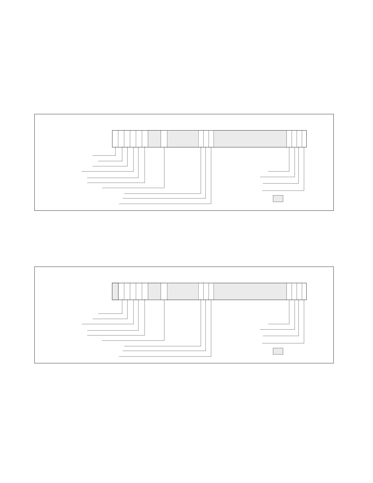
PERFORMANCE MONITORING
20.2.4.2 IA32_PERF_GLOBAL_STATUS_RESET and IA32_PERF_GLOBAL_STATUS_SET MSRS
With architectural performance monitoring version 3 and lower, clearing of the set bits in IA32_PERF_-
GLOBAL_STATUS MSR by software is done via IA32_PERF_GLOBAL_OVF_CTRL MSR. Starting with architectural
performance monitoring version 4, software can manage the overflow and other indicators in IA32_PERF_-
GLOBAL_STATUS using separate interfaces to set or clear individual bits.
The address and the architecturally-defined bits of IA32_PERF_GLOBAL_OVF_CTRL is inherited by IA32_PERF_-
GLOBAL_STATUS_RESET (see Figure 20-11). Further, IA32_PERF_GLOBAL_STATUS_RESET provides additional bit
fields to clear the new indicators in IA32_PERF_GLOBAL_STATUS described in Section 20.2.4.1.
6362
61
60 59 58
55
3534333231
N ..
10
Clr CondChgd
Clr OvfDSBuffer
Clr OvfUncore
Clr ASCI
Clr IA32_PMC(N-1) Ovf
Clr CTR_Frz
Clr
Ovf
Clr LBR_Frz
Clr IA32_PMC1 Ovf
Clr TraceToPAPMI
Clr IA32_PMC0 Ovf
Clr IA32_FIXED_CTR2 Ovf
Clr IA32_FIXED_CTR1 Ovf
Reserved
Clr IA32_FIXED_CTR0 Ovf
Figure 20-11. IA32_PERF_GLOBAL_STATUS_RESET MSR and Architectural Perfmon Version 4
The IA32_PERF_GLOBAL_STATUS_SET MSR is introduced with architectural performance monitoring version 4. It
allows software to set individual bits in IA32_PERF_GLOBAL_STATUS. The IA32_PERF_GLOBAL_STATUS_SET
interface can be used by a VMM to virtualize the state of IA32_PERF_GLOBAL_STATUS across VMs.
63 62 61 60 59 58
55
3534333231
N ..
10
Set OvfDSBuffer
Set OvfUncore
Set ASCI
Set IA32_PMC(N-1) Ovf
Set CTR_Frz
Set
Ovf
Set LBR_Frz
Set IA32_PMC1 Ovf
Set TraceToPAPMI
Set IA32_PMC0 Ovf
Set IA32_FIXED_CTR2 Ovf
Set IA32_FIXED_CTR1 Ovf
Reserved
Set IA32_FIXED_CTR0 Ovf
Figure 20-12. IA32_PERF_GLOBAL_STATUS_SET MSR and Architectural Perfmon Version 4
20.2.4.3 IA32_PERF_GLOBAL_INUSE MSR
In a contemporary software environment, multiple privileged service agents may wish to employ the processor’s
performance monitoring facilities. The IA32_MISC_ENABLE.PERFMON_AVAILABLE[bit 7] interface could not serve
Vol. 3B
20-15

PERFORMANCE MONITORING
the need of multiple agent adequately. A white paper, “Performance Monitoring Unit Sharing Guideline”1, proposed
a cooperative sharing protocol that is voluntary for participating software agents.
Architectural performance monitoring version 4 introduces a new MSR, IA32_PERF_GLOBAL_INUSE, that simplifies
the task of multiple cooperating agents to implement the sharing protocol.
The layout of IA32_PERF_GLOBAL_INUSE is shown in Figure 20-13.
63
3534333231
N ..
10
PMI InUse
FIXED_CTR2 InUse
PERFEVTSEL(N-1) InUse
FIXED_CTR1 InUse
....................... InUse
FIXED_CTR0 InUse
PERFEVTSEL1 InUse
PERFEVTSEL0 InUse
N = CPUID.0AH:EAX[15:8]
Reserved
Figure 20-13. IA32_PERF_GLOBAL_INUSE MSR and Architectural Perfmon Version 4
The IA32_PERF_GLOBAL_INUSE MSR provides an “InUse” bit for each programmable performance counter and
fixed counter in the processor. Additionally, it includes an indicator if the PMI mechanism has been configured by a
profiling agent.
• IA32_PERF_GLOBAL_INUSE.PERFEVTSEL0_InUse[bit 0]: This bit reflects the logical state of (IA32_PERFE-
VTSEL0[7:0] != 0).
• IA32_PERF_GLOBAL_INUSE.PERFEVTSEL1_InUse[bit 1]: This bit reflects the logical state of (IA32_PERFE-
VTSEL1[7:0] != 0).
• IA32_PERF_GLOBAL_INUSE.PERFEVTSEL2_InUse[bit 2]: This bit reflects the logical state of (IA32_PERFE-
VTSEL2[7:0] != 0).
• IA32_PERF_GLOBAL_INUSE.PERFEVTSELn_InUse[bit n]: This bit reflects the logical state of (IA32_PERFE-
VTSELn[7:0] != 0), n < CPUID.0AH:EAX[15:8].
• IA32_PERF_GLOBAL_INUSE.FC0_InUse[bit 32]: This bit reflects the logical state of (IA32_FIXED_C-
TR_CTRL[1:0] != 0).
• IA32_PERF_GLOBAL_INUSE.FC1_InUse[bit 33]: This bit reflects the logical state of (IA32_FIXED_C-
TR_CTRL[5:4] != 0).
• IA32_PERF_GLOBAL_INUSE.FC2_InUse[bit 34]: This bit reflects the logical state of (IA32_FIXED_C-
TR_CTRL[9:8] != 0).
• IA32_PERF_GLOBAL_INUSE.PMI_InUse[bit 63]: This bit is set if any one of the following bit is set:
— IA32_PERFEVTSELn.INT[bit 20], n < CPUID.0AH:EAX[15:8].
— IA32_FIXED_CTR_CTRL.ENi_PMI, i = 0, 1, 2.
— Any IA32_PEBS_ENABLES bit which enables PEBS for a general-purpose or fixed-function performance
counter.
1. Available at http://www.intel.com/sdm
20-16
Vol. 3B
PERFORMANCE MONITORING
20.2.5 Architectural Performance Monitoring Version 5
Processors supporting architectural performance monitoring version 5 also support versions 1, 2, 3, and 4, as well
as capability enumerated by CPUID leaf 0AH. Specifically, version 5 provides the following enhancements:
• Deprecation of AnyThread mode, see Section 20.2.5.1.
• Individual enumeration of Fixed counters in CPUID.0AH, see Section 20.2.5.2.
• Domain separation, see Section 20.2.5.3.
20.2.5.1 AnyThread Mode Deprecation
With Architectural Performance Monitoring Version 5, a processor that supports AnyThread mode deprecation is
enumerated by CPUID.0AH.EDX[15]. If set, software will not have to follow guidelines in Section 20.2.3.1.
20.2.5.2 Fixed Counter Enumeration
With Architectural Performance Monitoring Version 5, register CPUID.0AH.ECX indicates Fixed Counter enumera-
tion. It is a bit mask which enumerates the supported Fixed Counters in a processor. If bit 'i' is set, it implies that
Fixed Counter 'i' is supported. Software is recommended to use the following logic to check if a Fixed Counter is
supported on a given processor:
FxCtr[i]_is_supported := ECX[i] || (EDX[4:0] > i);
20.2.5.3 Domain Separation
When the INV flag in IA32_PERFEVTSELx is used, a counter stops counting when the logical processor exits the C0
ACPI C-state.
20.2.6 Full-Width Writes to Performance Counter Registers
The general-purpose performance counter registers IA32_PMCx are writable via WRMSR instruction. However, the
value written into IA32_PMCx by WRMSR is the signed extended 64-bit value of the EAX[31:0] input of WRMSR.
A processor that supports full-width writes to the general-purpose performance counters enumerated by
CPUID.0AH:EAX[15:8] will set IA32_PERF_CAPABILITIES[13] to enumerate its full-width-write capability See
Figure 20-65.
If IA32_PERF_CAPABILITIES.FW_WRITE[bit 13] =1, each IA32_PMCi is accompanied by a corresponding alias
address starting at 4C1H for IA32_A_PMC0.
The bit width of the performance monitoring counters is specified in CPUID.0AH:EAX[23:16].
If IA32_A_PMCi is present, the 64-bit input value (EDX:EAX) of WRMSR to IA32_A_PMCi will cause IA32_PMCi to
be updated by:
COUNTERWIDTH = CPUID.0AH:EAX[23:16] bit width of the performance monitoring counter
IA32_PMCi[COUNTERWIDTH-1:32] := EDX[COUNTERWIDTH-33:0]);
IA32_PMCi[31:0] := EAX[31:0];
EDX[63:COUNTERWIDTH] are reserved
20.3
PERFORMANCE MONITORING (INTEL® CORE™ PROCESSORS AND INTEL®
XEON® PROCESSORS)
20.3.1 Performance Monitoring for Processors Based on Nehalem Microarchitecture
Intel Core i7 processor family1 supports architectural performance monitoring capability with version ID 3 (see
Section 20.2.3) and a host of non-architectural monitoring capabilities. The Intel Core i7 processor family is based
Vol. 3B
20-17

PERFORMANCE MONITORING
on Nehalem microarchitecture, and provides four general-purpose performance counters (IA32_PMC0,
IA32_PMC1, IA32_PMC2, IA32_PMC3) and three fixed-function performance counters (IA32_FIXED_CTR0, IA32_-
FIXED_CTR1, IA32_FIXED_CTR2) in the processor core.
Non-architectural performance monitoring in Intel Core i7 processor family uses the IA32_PERFEVTSELx MSR to
configure a set of non-architecture performance monitoring events to be counted by the corresponding general-
purpose performance counter. The list of non-architectural performance monitoring events can be found at:
https://perfmon-events.intel.com/. Non-architectural performance monitoring events fall into two broad catego-
ries:
• Performance monitoring events in the processor core: These include many events that are similar to
performance monitoring events available to processor based on Intel Core microarchitecture. Additionally,
there are several enhancements in the performance monitoring capability for detecting microarchitectural
conditions in the processor core or in the interaction of the processor core to the off-core sub-systems in the
physical processor package. The off-core sub-systems in the physical processor package is loosely referred to
as “uncore“.
• Performance monitoring events in the uncore: The uncore sub-system is shared by more than one processor
cores in the physical processor package. It provides additional performance monitoring facility outside of
IA32_PMCx and performance monitoring events that are specific to the uncore sub-system.
Architectural and non-architectural performance monitoring events in Intel Core i7 processor family support thread
qualification using bit 21 of IA32_PERFEVTSELx MSR.
The bit fields within each IA32_PERFEVTSELx MSR are defined in Figure 20-6 and described in Section 20.2.1.1 and
Section 20.2.3.
63 62 6160
3534333231
8 7
6
5 4
3
2
1
0
CHG (R/W)
OVF_PMI (R/W)
OVF_FC2 (R/O)
OVF_FC1 (R/O)
OVF_FC0 (R/O)
OVF_PC7 (R/O), if CCNT>7
OVF_PC6 (R/O), if CCNT>6
OVF_PC5 (R/O), if CCNT>5
OVF_PC4 (R/O), if CCNT>4
OVF_PC3 (R/O)
OVF_PC2 (R/O)
OVF_PC1 (R/O)
OVF_PC0 (R/O)
Reserved
RESET Value — 00000000_00000000H
CCNT: CPUID.AH:EAX[15:8]
Figure 20-14. IA32_PERF_GLOBAL_STATUS MSR
20.3.1.1 Enhancements of Performance Monitoring in the Processor Core
The notable enhancements in the monitoring of performance events in the processor core include:
• Four general purpose performance counters, IA32_PMCx, associated counter configuration MSRs, IA32_PERFE-
VTSELx, and global counter control MSR supporting simplified control of four counters. Each of the four
performance counter can support processor event based sampling (PEBS) and thread-qualification of architec-
tural and non-architectural performance events. Width of IA32_PMCx supported by hardware has been
increased. The width of counter reported by CPUID.0AH:EAX[23:16] is 48 bits. The PEBS facility in Nehalem
1. Intel Xeon processor 5500 series and 3400 series are also based on Nehalem microarchitecture; the performance monitoring facili-
ties described in this section generally also apply.
20-18
Vol. 3B