Intel 64 and IA-32 Architectures. Software Developer’s Manual (Collection, 2023) - page 52

ADVANCED PROGRAMMABLE INTERRUPT CONTROLLER (APIC)
Table 11-9. Short Message (21 Cycles) (Contd.)
Cycle
Bit1
Bit0
17
C
C
Checksum for cycles 6-16
18
0
0
19
A
A
Status cycle 0
20
A1
A1
Status cycle 1
21
0
0
Idle
If the physical delivery mode is being used, then cycles 15 and 16 represent the APIC ID and cycles 13 and 14 are
considered don't care by the receiver. If the logical delivery mode is being used, then cycles 13 through 16 are the
8-bit logical destination field.
For shorthands of “all-incl-self” and “all-excl-self,” the physical delivery mode and an arbitration priority of 15
(D0:D3 = 1111) are used. The agent sending the message is the only one required to distinguish between the two
cases. It does so using internal information.
When using lowest priority delivery with an existing focus processor, the focus processor identifies itself by driving
10 during cycle 19 and accepts the interrupt. This is an indication to other APICs to terminate arbitration. If the
focus processor has not been found, the short message is extended on-the-fly to the non-focused lowest-priority
message. Note that except for the EOI message, messages generating a checksum or an acceptance error (see
Section 11.5.3, “Error Handling”) terminate after cycle 21.
11.13.2.2 Non-focused Lowest Priority Message
These 34-cycle messages (see Table 11-10) are used in the lowest priority delivery mode when a focus processor
is not present. Cycles 1 through 20 are same as for the short message. If during the status cycle (cycle 19) the
state of the (A:A) flags is 10B, a focus processor has been identified, and the short message format is used (see
Table 11-9). If the (A:A) flags are set to 00B, lowest priority arbitration is started and the 34-cycles of the non-
focused lowest priority message are competed. For other combinations of status flags, refer to Section 11.13.2.3,
“APIC Bus Status Cycles.”
Table 11-10. Non-Focused Lowest Priority Message (34 Cycles)
Cycle
Bit0
Bit1
1
0
1
0 1 = normal
2
ArbID3
0
Arbitration ID bits 3 through 0
3
ArbID2
0
4
ArbID1
0
5
ArbID0
0
6
DM
M2
DM = Destination mode
7
M1
M0
M2-M0 = Delivery mode
8
L
TM
L = Level, TM = Trigger Mode
9
V7
V6
V7-V0 = Interrupt Vector
10
V5
V4
11
V3
V2
12
V1
V0
13
D7
D6
D7-D0 = Destination
14
D5
D4
15
D3
D2
16
D1
D0
Vol. 3A
11-49

ADVANCED PROGRAMMABLE INTERRUPT CONTROLLER (APIC)
Table 11-10. Non-Focused Lowest Priority Message (34 Cycles) (Contd.)
Cycle
Bit0
Bit1
17
C
C
Checksum for cycles 6-16
18
0
0
19
A
A
Status cycle 0
20
A1
A1
Status cycle 1
21
P7
0
P7 - P0 = Inverted Processor Priority
22
P6
0
23
P5
0
24
P4
0
25
P3
0
26
P2
0
27
P1
0
28
P0
0
29
ArbID3
0
Arbitration ID 3 -0
30
ArbID2
0
31
ArbID1
0
32
ArbID0
0
33
A2
A2
Status Cycle
34
0
0
Idle
Cycles 21 through 28 are used to arbitrate for the lowest priority processor. The processors participating in the arbi-
tration drive their inverted processor priority on the bus. Only the local APICs having free interrupt slots participate
in the lowest priority arbitration. If no such APIC exists, the message will be rejected, requiring it to be tried at a
later time.
Cycles 29 through 32 are also used for arbitration in case two or more processors have the same lowest priority. In
the lowest priority delivery mode, all combinations of errors in cycle 33 (A2 A2) will set the “accept error” bit in the
error status register (see Figure 11-9). Arbitration priority update is performed in cycle 20, and is not affected by
errors detected in cycle 33. Only the local APIC that wins in the lowest priority arbitration, drives cycle 33. An error
in cycle 33 will force the sender to resend the message.
11.13.2.3 APIC Bus Status Cycles
Certain cycles within an APIC bus message are status cycles. During these cycles the status flags (A:A) and
(A1:A1) are examined. Table 11-11 shows how these status flags are interpreted, depending on the current
delivery mode and existence of a focus processor.
11-50
Vol. 3A

ADVANCED PROGRAMMABLE INTERRUPT CONTROLLER (APIC)
Table 11-11. APIC Bus Status Cycles Interpretation
Delivery
A Status
A1 Status
A2 Status
Update ArbID
Message
Retry
Mode
and Cycle#
Length
EOI
00: CS_OK
10: Accept
XX:
Yes, 13
14 Cycle
No
00: CS_OK
11: Retry
XX:
Yes, 13
14 Cycle
Yes
00: CS_OK
0X: Accept Error
XX:
No
14 Cycle
Yes
11: CS_Error
XX:
XX:
No
14 Cycle
Yes
10: Error
XX:
XX:
No
14 Cycle
Yes
01: Error
XX:
XX:
No
14 Cycle
Yes
Fixed
00: CS_OK
10: Accept
XX:
Yes, 20
21 Cycle
No
00: CS_OK
11: Retry
XX:
Yes, 20
21 Cycle
Yes
00: CS_OK
0X: Accept Error
XX:
No
21 Cycle
Yes
11: CS_Error
XX:
XX:
No
21 Cycle
Yes
10: Error
XX:
XX:
No
21 Cycle
Yes
01: Error
XX:
XX:
No
21 Cycle
Yes
NMI, SMI, INIT,
00: CS_OK
10: Accept
XX:
Yes, 20
21 Cycle
No
ExtINT,
00: CS_OK
11: Retry
XX:
Yes, 20
21 Cycle
Yes
Start-Up
00: CS_OK
0X: Accept Error
XX:
No
21 Cycle
Yes
11: CS_Error
XX:
XX:
No
21 Cycle
Yes
10: Error
XX:
XX:
No
21 Cycle
Yes
01: Error
XX:
XX:
No
21 Cycle
Yes
Lowest
00: CS_OK, NoFocus
11: Do Lowest
10: Accept
Yes, 20
34 Cycle
No
00: CS_OK, NoFocus
11: Do Lowest
11: Error
Yes, 20
34 Cycle
Yes
00: CS_OK, NoFocus
11: Do Lowest
0X: Error
Yes, 20
34 Cycle
Yes
00: CS_OK, NoFocus
10: End and Retry
XX:
Yes, 20
34 Cycle
Yes
00: CS_OK, NoFocus
0X: Error
XX:
No
34 Cycle
Yes
10: CS_OK, Focus
XX:
XX:
Yes, 20
34 Cycle
No
11: CS_Error
XX:
XX:
No
21 Cycle
Yes
01: Error
XX:
XX:
No
21 Cycle
Yes
Vol. 3A
11-51
ADVANCED PROGRAMMABLE INTERRUPT CONTROLLER (APIC)
11-52
Vol. 3A
CHAPTER 12
MEMORY CACHE CONTROL
This chapter describes the memory cache and cache control mechanisms, the TLBs, and the store buffer in Intel 64
and IA-32 processors. It also describes the memory type range registers (MTRRs) introduced in the P6 family
processors and how they are used to control caching of physical memory locations.
12.1
INTERNAL CACHES, TLBS, AND BUFFERS
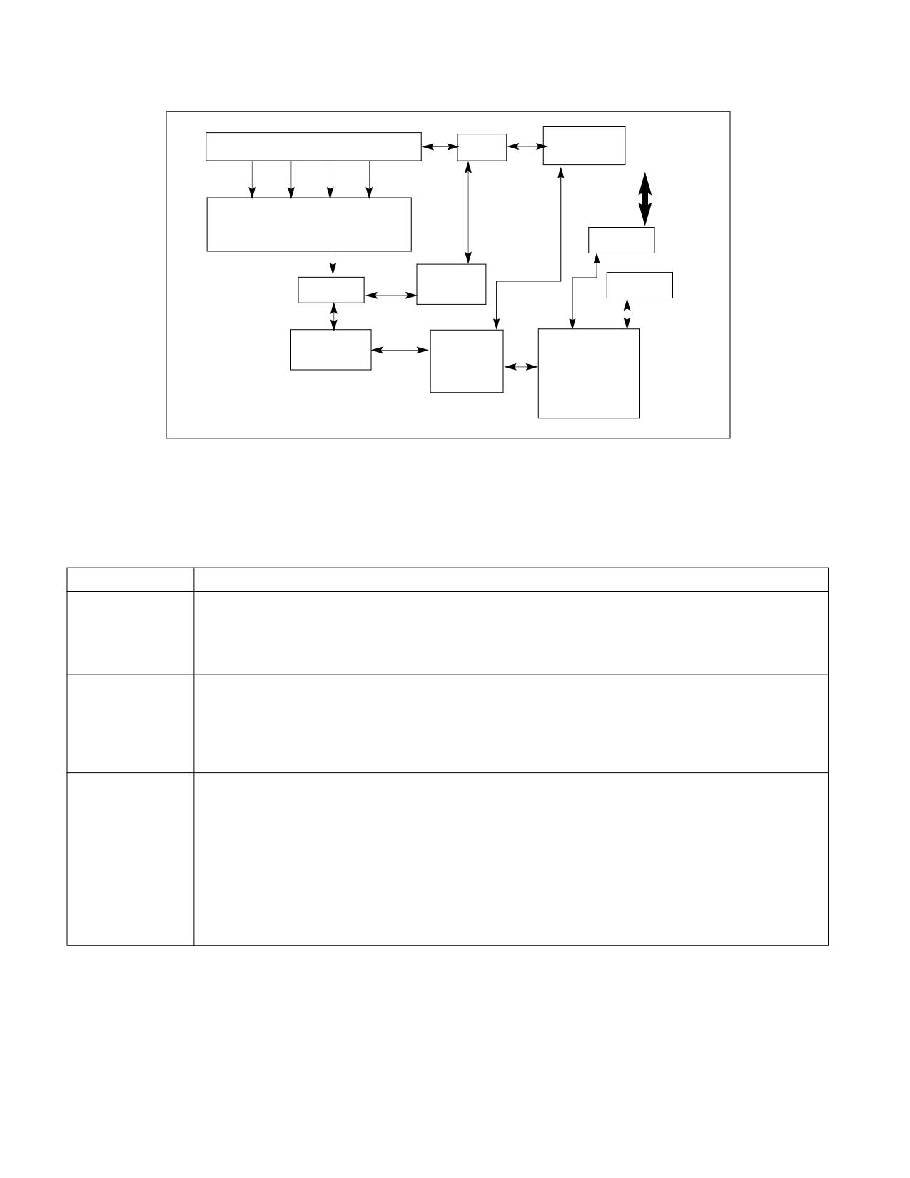
The Intel 64 and IA-32 architectures support cache, translation look aside buffers (TLBs), and a store buffer for
temporary on-chip (and external) storage of instructions and data. (Figure 12-1 shows the arrangement of caches,
TLBs, and the store buffer for the Pentium 4 and Intel Xeon processors.) Table 12-1 shows the characteristics of
these caches and buffers for the Pentium 4, Intel Xeon, P6 family, and Pentium processors. The sizes and char-
acteristics of these units are machine specific and may change in future versions of the processor. The
CPUID instruction returns the sizes and characteristics of the caches and buffers for the processor on which the
instruction is executed. See “CPUID-CPU Identification” in Chapter 3, “Instruction Set Reference, A-L,” of the
Intel® 64 and IA-32 Architectures Software Developer’s Manual, Volume 2A.
Physical
Memory
System Bus
(External)
Data Cache
L2 Cache
L3 Cache
†
Unit (L1)
Instruction
TLBs
Bus Interface Unit
Data TLBs
Instruction Decoder
Trace Cache
Store Buffer
† Intel Xeon processors only
Figure 12-1. Cache Structure of the Pentium 4 and Intel Xeon Processors
Vol. 3A
12-1
MEMORY CACHE CONTROL
Instruction
Instruction Decoder and front end
ITLB
Cache
Chipset
Out-of-Order Engine
QPI
STLB
IMC
Data TLB
Data Cache
Unit (L1)
L2 Cache
L3 Cache
Figure 12-2. Cache Structure of the Intel Core i7 Processors
Figure 12-2 shows the cache arrangement of Intel Core i7 processor.
Table 12-1. Characteristics of the Caches, TLBs, Store Buffer, and
Write Combining Buffer in Intel 64 and IA-32 Processors
Cache or Buffer
Characteristics
Trace Cache1
• Pentium 4 and Intel Xeon processors (Based on Intel NetBurst® microarchitecture): 12 Kμops, 8-way set
associative.
• Intel Core i7, Intel Core 2 Duo, Intel Atom, Intel Core Duo, Intel Core Solo, Pentium M processor: not
implemented.
• P6 family and Pentium processors: not implemented.
L1 Instruction Cache
• Pentium 4 and Intel Xeon processors (Based on Intel NetBurst microarchitecture): not implemented.
• Intel Core i7 processor: 32-KByte, 4-way set associative.
• Intel Core 2 Duo, Intel Atom, Intel Core Duo, Intel Core Solo, Pentium M processor: 32-KByte, 8-way set
associative.
• P6 family and Pentium processors: 8- or 16-KByte, 4-way set associative, 32-byte cache line size; 2-way set
associative for earlier Pentium processors.
L1 Data Cache
• Pentium 4 and Intel Xeon processors (Based on Intel NetBurst microarchitecture): 8-KByte, 4-way set
associative, 64-byte cache line size.
• Pentium 4 and Intel Xeon processors (Based on Intel NetBurst microarchitecture): 16-KByte, 8-way set
associative, 64-byte cache line size.
• Intel Atom processors: 24-KByte, 6-way set associative, 64-byte cache line size.
• Intel Core i7, Intel Core 2 Duo, Intel Core Duo, Intel Core Solo, Pentium M and Intel Xeon processors: 32-
KByte, 8-way set associative, 64-byte cache line size.
• P6 family processors: 16-KByte, 4-way set associative, 32-byte cache line size; 8-KBytes, 2-way set
associative for earlier P6 family processors.
• Pentium processors: 16-KByte, 4-way set associative, 32-byte cache line size; 8-KByte, 2-way set
associative for earlier Pentium processors.
12-2
Vol. 3A
MEMORY CACHE CONTROL
Table 12-1. Characteristics of the Caches, TLBs, Store Buffer, and
Write Combining Buffer in Intel 64 and IA-32 Processors (Contd.)
Cache or Buffer
Characteristics
L2 Unified Cache
•
Intel Core 2 Duo and Intel Xeon processors: up to 4-MByte (or 4MBx2 in quadcore processors), 16-way set
associative, 64-byte cache line size.
•
Intel Core 2 Duo and Intel Xeon processors: up to 6-MByte (or 6MBx2 in quadcore processors), 24-way set
associative, 64-byte cache line size.
•
Intel Core i7, i5, i3 processors: 256KBbyte, 8-way set associative, 64-byte cache line size.
•
Intel Atom processors: 512-KByte, 8-way set associative, 64-byte cache line size.
•
Intel Core Duo, Intel Core Solo processors: 2-MByte, 8-way set associative, 64-byte cache line size
•
Pentium 4 and Intel Xeon processors: 256, 512, 1024, or 2048-KByte, 8-way set associative, 64-byte cache
line size, 128-byte sector size.
•
Pentium M processor: 1 or 2-MByte, 8-way set associative, 64-byte cache line size.
•
P6 family processors: 128-KByte, 256-KByte, 512-KByte, 1-MByte, or 2-MByte, 4-way set associative,
32-byte cache line size.
•
Pentium processor (external optional): System specific, typically 256- or 512-KByte, 4-way set associative,
32-byte cache line size.
L3 Unified Cache
•
Intel Xeon processors: 512-KByte, 1-MByte, 2-MByte, or 4-MByte, 8-way set associative, 64-byte cache line
size, 128-byte sector size.
•
Intel Core i7 processor, Intel Xeon processor 5500: Up to 8MByte, 16-way set associative, 64-byte cache
line size.
•
Intel Xeon processor 5600: Up to 12MByte, 64-byte cache line size.
•
Intel Xeon processor 7500: Up to 24MByte, 64-byte cache line size.
Instruction TLB
•
Pentium 4 and Intel Xeon processors (Based on Intel NetBurst microarchitecture): 128 entries, 4-way set
(4-KByte Pages)
associative.
•
Intel Atom processors: 32-entries, fully associative.
•
Intel Core i7, i5, i3 processors: 64-entries per thread (128-entries per core), 4-way set associative.
•
Intel Core 2 Duo, Intel Core Duo, Intel Core Solo processors, Pentium M processor: 128 entries, 4-way set
associative.
•
P6 family processors: 32 entries, 4-way set associative.
•
Pentium processor: 32 entries, 4-way set associative; fully set associative for Pentium processors with MMX
technology.
Data TLB (4-KByte
•
Intel Core i7, i5, i3 processors, DTLB0: 64-entries, 4-way set associative.
Pages)
•
Intel Core 2 Duo processors: DTLB0, 16 entries, DTLB1, 256 entries, 4 ways.
•
Intel Atom processors: 16-entry-per-thread micro-TLB, fully associative; 64-entry DTLB, 4-way set
associative; 16-entry PDE cache, fully associative.
•
Pentium 4 and Intel Xeon processors (Based on Intel NetBurst microarchitecture): 64 entry, fully set
associative, shared with large page DTLB.
•
Intel Core Duo, Intel Core Solo processors, Pentium M processor: 128 entries, 4-way set associative.
•
Pentium and P6 family processors: 64 entries, 4-way set associative; fully set, associative for Pentium
processors with MMX technology.
Instruction TLB
•
Intel Core i7, i5, i3 processors: 7-entries per thread, fully associative.
(Large Pages)
•
Intel Core 2 Duo processors: 4 entries, 4 ways.
•
Pentium 4 and Intel Xeon processors: large pages are fragmented.
•
Intel Core Duo, Intel Core Solo, Pentium M processor: 2 entries, fully associative.
•
P6 family processors: 2 entries, fully associative.
•
Pentium processor: Uses same TLB as used for 4-KByte pages.
Data TLB (Large
•
Intel Core i7, i5, i3 processors, DTLB0: 32-entries, 4-way set associative.
Pages)
•
Intel Core 2 Duo processors: DTLB0, 16 entries, DTLB1, 32 entries, 4 ways.
•
Intel Atom processors: 8 entries, 4-way set associative.
•
Pentium 4 and Intel Xeon processors: 64 entries, fully set associative; shared with small page data TLBs.
•
Intel Core Duo, Intel Core Solo, Pentium M processor: 8 entries, fully associative.
•
P6 family processors: 8 entries, 4-way set associative.
•
Pentium processor: 8 entries, 4-way set associative; uses same TLB as used for 4-KByte pages in Pentium
processors with MMX technology.
Second-level Unified
•
Intel Core i7, i5, i3 processor, STLB: 512-entries, 4-way set associative.
TLB (4-KByte
Pages)
Vol. 3A
12-3
MEMORY CACHE CONTROL
Table 12-1. Characteristics of the Caches, TLBs, Store Buffer, and
Write Combining Buffer in Intel 64 and IA-32 Processors (Contd.)
Cache or Buffer
Characteristics
Store Buffer
• Intel Core i7, i5, i3 processors: 32entries.
• Intel Core 2 Duo processors: 20 entries.
• Intel Atom processors: 8 entries, used for both WC and store buffers.
• Pentium 4 and Intel Xeon processors: 24 entries.
• Pentium M processor: 16 entries.
• P6 family processors: 12 entries.
• Pentium processor: 2 buffers, 1 entry each (Pentium processors with MMX technology have 4 buffers for 4
entries).
Write Combining
• Intel Core 2 Duo processors: 8 entries.
(WC) Buffer
• Intel Atom processors: 8 entries, used for both WC and store buffers.
• Pentium 4 and Intel Xeon processors: 6 or 8 entries.
• Intel Core Duo, Intel Core Solo, Pentium M processors: 6 entries.
• P6 family processors: 4 entries.
NOTES:
1 Introduced to the IA-32 architecture in the Pentium 4 and Intel Xeon processors.
Intel 64 and IA-32 processors may implement four types of caches: the trace cache, the level 1 (L1) cache, the
level 2 (L2) cache, and the level 3 (L3) cache. See Figure 12-1. Cache availability is described below:
• Intel Core i7, i5, i3 processor family and Intel Xeon processor family based on Nehalem microarchi-
tecture and Westmere microarchitecture - The L1 cache is divided into two sections: one section is
dedicated to caching instructions (pre-decoded instructions) and the other caches data. The L2 cache is a
unified data and instruction cache. Each processor core has its own L1 and L2. The L3 cache is an inclusive,
unified data and instruction cache, shared by all processor cores inside a physical package. No trace cache is
implemented.
• Intel® Core™ 2 processor family and Intel® Xeon® processor family based on Intel® Core™ micro-
architecture - The L1 cache is divided into two sections: one section is dedicated to caching instructions (pre-
decoded instructions) and the other caches data. The L2 cache is a unified data and instruction cache located
on the processor chip; it is shared between two processor cores in a dual-core processor implementation.
Quad-core processors have two L2, each shared by two processor cores. No trace cache is implemented.
• Intel Atom® processor - The L1 cache is divided into two sections: one section is dedicated to caching
instructions (pre-decoded instructions) and the other caches data. The L2 cache is a unified data and
instruction cache is located on the processor chip. No trace cache is implemented.
• Intel® Core™ Solo and Intel® Core™ Duo processors - The L1 cache is divided into two sections: one
section is dedicated to caching instructions (pre-decoded instructions) and the other caches data. The L2 cache
is a unified data and instruction cache located on the processor chip. It is shared between two processor cores
in a dual-core processor implementation. No trace cache is implemented.
• Pentium® 4 and Intel® Xeon® processors Based on Intel NetBurst® microarchitecture - The trace
cache caches decoded instructions (μops) from the instruction decoder and the L1 cache contains data. The L2
and L3 caches are unified data and instruction caches located on the processor chip. Dualcore processors have
two L2, one in each processor core. Note that the L3 cache is only implemented on some Intel Xeon processors.
• P6 family processors - The L1 cache is divided into two sections: one dedicated to caching instructions (pre-
decoded instructions) and the other to caching data. The L2 cache is a unified data and instruction cache
located on the processor chip. P6 family processors do not implement a trace cache.
• Pentium® processors - The L1 cache has the same structure as on P6 family processors. There is no trace
cache. The L2 cache is a unified data and instruction cache external to the processor chip on earlier Pentium
processors and implemented on the processor chip in later Pentium processors. For Pentium processors where
the L2 cache is external to the processor, access to the cache is through the system bus.
For Intel Core i7 processors and processors based on Intel Core, Intel Atom, and Intel NetBurst microarchitectures,
Intel Core Duo, Intel Core Solo and Pentium M processors, the cache lines for the L1 and L2 caches (and L3 caches
if supported) are 64 bytes wide. The processor always reads a cache line from system memory beginning on a 64-
byte boundary. (A 64-byte aligned cache line begins at an address with its 6 least-significant bits clear.) A cache
12-4
Vol. 3A
MEMORY CACHE CONTROL
line can be filled from memory with a 8-transfer burst transaction. The caches do not support partially-filled cache
lines, so caching even a single doubleword requires caching an entire line.
The L1 and L2 cache lines in the P6 family and Pentium processors are 32 bytes wide, with cache line reads from
system memory beginning on a 32-byte boundary (5 least-significant bits of a memory address clear.) A cache line
can be filled from memory with a 4-transfer burst transaction. Partially-filled cache lines are not supported.
The trace cache in processors based on Intel NetBurst microarchitecture is available in all execution modes:
protected mode, system management mode (SMM), and real-address mode. The L1,L2, and L3 caches are also
available in all execution modes; however, use of them must be handled carefully in SMM (see Section 32.4.2,
“SMRAM Caching”).
The TLBs store the most recently used page-directory and page-table entries. They speed up memory accesses
when paging is enabled by reducing the number of memory accesses that are required to read the page tables
stored in system memory. The TLBs are divided into four groups: instruction TLBs for 4-KByte pages, data TLBs for
4-KByte pages; instruction TLBs for large pages (2-MByte, 4-MByte or 1-GByte pages), and data TLBs for large
pages. The TLBs are normally active only in protected mode with paging enabled. When paging is disabled or the
processor is in real-address mode, the TLBs maintain their contents until explicitly or implicitly flushed (see Section
12.9, “Invalidating the Translation Lookaside Buffers (TLBs)”).
Processors based on Intel Core microarchitectures implement one level of instruction TLB and two levels of data
TLB. Intel Core i7 processor provides a second-level unified TLB.
The store buffer is associated with the processors instruction execution units. It allows writes to system memory
and/or the internal caches to be saved and in some cases combined to optimize the processor’s bus accesses. The
store buffer is always enabled in all execution modes.
The processor’s caches are for the most part transparent to software. When enabled, instructions and data flow
through these caches without the need for explicit software control. However, knowledge of the behavior of these
caches may be useful in optimizing software performance. For example, knowledge of cache dimensions and
replacement algorithms gives an indication of how large of a data structure can be operated on at once without
causing cache thrashing.
In multiprocessor systems, maintenance of cache consistency may, in rare circumstances, require intervention by
system software. For these rare cases, the processor provides privileged cache control instructions for use in
flushing caches and forcing memory ordering.
There are several instructions that software can use to improve the performance of the L1, L2, and L3 caches,
including the PREFETCHh, CLFLUSH, and CLFLUSHOPT instructions and the non-temporal move instructions
(MOVNTI, MOVNTQ, MOVNTDQ, MOVNTPS, and MOVNTPD). The use of these instructions are discussed in Section
12.5.5, “Cache Management Instructions.”
12.2
CACHING TERMINOLOGY
IA-32 processors (beginning with the Pentium processor) and Intel 64 processors use the MESI (modified, exclu-
sive, shared, invalid) cache protocol to maintain consistency with internal caches and caches in other processors
(see Section 12.4, “Cache Control Protocol”).
When the processor recognizes that an operand being read from memory is cacheable, the processor reads an
entire cache line into the appropriate cache (L1, L2, L3, or all). This operation is called a cache line fill. If the
memory location containing that operand is still cached the next time the processor attempts to access the
operand, the processor can read the operand from the cache instead of going back to memory. This operation is
called a cache hit.
When the processor attempts to write an operand to a cacheable area of memory, it first checks if a cache line for
that memory location exists in the cache. If a valid cache line does exist, the processor (depending on the write
policy currently in force) can write the operand into the cache instead of writing it out to system memory. This
operation is called a write hit. If a write misses the cache (that is, a valid cache line is not present for area of
memory being written to), the processor performs a cache line fill, write allocation. Then it writes the operand into
the cache line and (depending on the write policy currently in force) can also write it out to memory. If the operand
is to be written out to memory, it is written first into the store buffer, and then written from the store buffer to
memory when the system bus is available. (Note that for the Pentium processor, write misses do not result in a
cache line fill; they always result in a write to memory. For this processor, only read misses result in cache line fills.)
Vol. 3A
12-5
MEMORY CACHE CONTROL
When operating in an MP system, IA-32 processors (beginning with the Intel486 processor) and Intel 64 processors
have the ability to snoop other processor’s accesses to system memory and to their internal caches. They use this
snooping ability to keep their internal caches consistent both with system memory and with the caches in other
processors on the bus. For example, in the Pentium and P6 family processors, if through snooping one processor
detects that another processor intends to write to a memory location that it currently has cached in shared state,
the snooping processor will invalidate its cache line forcing it to perform a cache line fill the next time it accesses
the same memory location.
Beginning with the P6 family processors, if a processor detects (through snooping) that another processor is trying
to access a memory location that it has modified in its cache, but has not yet written back to system memory, the
snooping processor will signal the other processor (by means of the HITM# signal) that the cache line is held in
modified state and will perform an implicit write-back of the modified data. The implicit write-back is transferred
directly to the initial requesting processor and snooped by the memory controller to assure that system memory
has been updated. Here, the processor with the valid data may pass the data to the other processors without actu-
ally writing it to system memory; however, it is the responsibility of the memory controller to snoop this operation
and update memory.
12.3
METHODS OF CACHING AVAILABLE
The processor allows any area of system memory to be cached in the L1, L2, and L3 caches. In individual pages or
regions of system memory, it allows the type of caching (also called memory type) to be specified (see Section
12.5). Memory types currently defined for the Intel 64 and IA-32 architectures are (see Table 12-2):
• Strong Uncacheable (UC) -System memory locations are not cached. All reads and writes appear on the
system bus and are executed in program order without reordering. No speculative memory accesses, page-
table walks, or prefetches of speculated branch targets are made. This type of cache-control is useful for
memory-mapped I/O devices. When used with normal RAM, it greatly reduces processor performance.
NOTE
The behavior of x87 and SIMD instructions referencing memory is implementation dependent. In
some implementations, accesses to UC memory may occur more than once. To ensure predictable
behavior, use loads and stores of general purpose registers to access UC memory that may have
read or write side effects.
Table 12-2. Memory Types and Their Properties
Memory Type and
Cacheable
Writeback
Allows
Memory Ordering Model
Mnemonic
Cacheable
Speculative
Reads
Strong Uncacheable
No
No
No
Strong Ordering
(UC)
Uncacheable (UC-)
No
No
No
Strong Ordering. Can only be selected through the PAT. Can be
overridden by WC in MTRRs.
Write Combining (WC)
No
No
Yes
Weak Ordering. Available by programming MTRRs or by selecting it
through the PAT.
Write Through (WT)
Yes
No
Yes
Speculative Processor Ordering.
Write Back (WB)
Yes
Yes
Yes
Speculative Processor Ordering.
Write Protected (WP)
Yes for
No
Yes
Speculative Processor Ordering. Available by programming MTRRs.
reads; no for
writes
• Uncacheable (UC-) - Has same characteristics as the strong uncacheable (UC) memory type, except that
this memory type can be overridden by programming the MTRRs for the WC memory type. This memory type
is available in processor families starting from the Pentium III processors and can only be selected through the
PAT.
12-6
Vol. 3A
MEMORY CACHE CONTROL
•
Write Combining (WC) - System memory locations are not cached (as with uncacheable memory) and
coherency is not enforced by the processor’s bus coherency protocol. Speculative reads are allowed. Writes
may be delayed and combined in the write combining buffer (WC buffer) to reduce memory accesses. If the WC
buffer is partially filled, the writes may be delayed until the next occurrence of a serializing event; such as an
SFENCE or MFENCE instruction, CPUID or other serializing instruction, a read or write to uncached memory, an
interrupt occurrence, or an execution of a LOCK instruction (including one with an XACQUIRE or XRELEASE
prefix). In addition, an execution of the XEND instruction (to end a transactional region) evicts any writes that
were buffered before the corresponding execution of the XBEGIN instruction (to begin the transactional region)
before evicting any writes that were performed inside the transactional region.
This type of cache-control is appropriate for video frame buffers, where the order of writes is unimportant as
long as the writes update memory so they can be seen on the graphics display. See Section 12.3.1, “Buffering
of Write Combining Memory Locations,” for more information about caching the WC memory type. This memory
type is available in the Pentium Pro and Pentium II processors by programming the MTRRs; or in processor
families starting from the Pentium III processors by programming the MTRRs or by selecting it through the PAT.
•
Write-through (WT) - Writes and reads to and from system memory are cached. Reads come from cache
lines on cache hits; read misses cause cache fills. Speculative reads are allowed. All writes are written to a
cache line (when possible) and through to system memory. When writing through to memory, invalid cache
lines are never filled, and valid cache lines are either filled or invalidated. Write combining is allowed. This type
of cache-control is appropriate for frame buffers or when there are devices on the system bus that access
system memory, but do not perform snooping of memory accesses. It enforces coherency between caches in
the processors and system memory.
•
Write-back (WB) - Writes and reads to and from system memory are cached. Reads come from cache lines
on cache hits; read misses cause cache fills. Speculative reads are allowed. Write misses cause cache line fills
(in processor families starting with the P6 family processors), and writes are performed entirely in the cache,
when possible. Write combining is allowed. The write-back memory type reduces bus traffic by eliminating
many unnecessary writes to system memory. Writes to a cache line are not immediately forwarded to system
memory; instead, they are accumulated in the cache. The modified cache lines are written to system memory
later, when a write-back operation is performed. Write-back operations are triggered when cache lines need to
be deallocated, such as when new cache lines are being allocated in a cache that is already full. They also are
triggered by the mechanisms used to maintain cache consistency. This type of cache-control provides the best
performance, but it requires that all devices that access system memory on the system bus be able to snoop
memory accesses to ensure system memory and cache coherency.
•
Write protected (WP) - Reads come from cache lines when possible, and read misses cause cache fills.
Writes are propagated to the system bus and cause corresponding cache lines on all processors on the bus to
be invalidated. Speculative reads are allowed. This memory type is available in processor families starting from
the P6 family processors by programming the MTRRs (see Table 12-6).
Table 12-3 shows which of these caching methods are available in the Pentium, P6 Family, Pentium 4, and Intel
Xeon processors.
Table 12-3. Methods of Caching Available in Intel Core 2 Duo, Intel Atom, Intel Core Duo, Pentium M, Pentium 4,
Intel Xeon, P6 Family, and Pentium Processors
Memory Type
Intel Core 2 Duo, Intel Atom, Intel Core Duo,
P6 Family
Pentium
Pentium M, Pentium 4 and Intel Xeon Processors
Processors
Processor
Strong Uncacheable (UC)
Yes
Yes
Yes
Uncacheable (UC-)
Yes
Yes*
No
Write Combining (WC)
Yes
Yes
No
Write Through (WT)
Yes
Yes
Yes
Write Back (WB)
Yes
Yes
Yes
Write Protected (WP)
Yes
Yes
No
NOTE:
* Introduced in the Pentium III processor; not available in the Pentium Pro or Pentium II processors
Vol. 3A
12-7
MEMORY CACHE CONTROL
12.3.1 Buffering of Write Combining Memory Locations
Writes to the WC memory type are not cached in the typical sense of the word cached. They are retained in an
internal write combining buffer (WC buffer) that is separate from the internal L1, L2, and L3 caches and the store
buffer. The WC buffer is not snooped and thus does not provide data coherency. Buffering of writes to WC memory
is done to allow software a small window of time to supply more modified data to the WC buffer while remaining as
non-intrusive to software as possible. The buffering of writes to WC memory also causes data to be collapsed; that
is, multiple writes to the same memory location will leave the last data written in the location and the other writes
will be lost.
The size and structure of the WC buffer is not architecturally defined. For the Intel Core 2 Duo, Intel Atom, Intel
Core Duo, Pentium M, Pentium 4 and Intel Xeon processors; the WC buffer is made up of several 64-byte WC
buffers. For the P6 family processors, the WC buffer is made up of several 32-byte WC buffers.
When software begins writing to WC memory, the processor begins filling the WC buffers one at a time. When one
or more WC buffers has been filled, the processor has the option of evicting the buffers to system memory. The
protocol for evicting the WC buffers is implementation dependent and should not be relied on by software for
system memory coherency. When using the WC memory type, software must be sensitive to the fact that the
writing of data to system memory is being delayed and must deliberately empty the WC buffers when system
memory coherency is required.
Once the processor has started to evict data from the WC buffer into system memory, it will make a bus-transaction
style decision based on how much of the buffer contains valid data. If the buffer is full (for example, all bytes are
valid), the processor will execute a burst-write transaction on the bus. This results in all 32 bytes (P6 family proces-
sors) or 64 bytes (Pentium 4 and more recent processor) being transmitted on the data bus in a single burst trans-
action. If one or more of the WC buffer’s bytes are invalid (for example, have not been written by software), the
processor will transmit the data to memory using “partial write” transactions (one chunk at a time, where a “chunk”
is 8 bytes).
This will result in a maximum of 4 partial write transactions (for P6 family processors) or 8 partial write transactions
(for the Pentium 4 and more recent processors) for one WC buffer of data sent to memory.
The WC memory type is weakly ordered by definition. Once the eviction of a WC buffer has started, the data is
subject to the weak ordering semantics of its definition. Ordering is not maintained between the successive alloca-
tion/deallocation of WC buffers (for example, writes to WC buffer 1 followed by writes to WC buffer 2 may appear
as buffer 2 followed by buffer 1 on the system bus). When a WC buffer is evicted to memory as partial writes there
is no guaranteed ordering between successive partial writes (for example, a partial write for chunk 2 may appear
on the bus before the partial write for chunk 1 or vice versa).
The only elements of WC propagation to the system bus that are guaranteed are those provided by transaction
atomicity. For example, with a P6 family processor, a completely full WC buffer will always be propagated as a
single 32-bit burst transaction using any chunk order. In a WC buffer eviction where data will be evicted as partials,
all data contained in the same chunk (0 mod 8 aligned) will be propagated simultaneously. Likewise, for more
recent processors starting with those based on Intel NetBurst microarchitectures, a full WC buffer will always be
propagated as a single burst transactions, using any chunk order within a transaction. For partial buffer propaga-
tions, all data contained in the same chunk will be propagated simultaneously.
12.3.2 Choosing a Memory Type
The simplest system memory model does not use memory-mapped I/O with read or write side effects, does not
include a frame buffer, and uses the write-back memory type for all memory. An I/O agent can perform direct
memory access (DMA) to write-back memory and the cache protocol maintains cache coherency.
A system can use strong uncacheable memory for other memory-mapped I/O, and should always use strong unca-
cheable memory for memory-mapped I/O with read side effects.
Dual-ported memory can be considered a write side effect, making relatively prompt writes desirable, because
those writes cannot be observed at the other port until they reach the memory agent. A system can use strong
uncacheable, uncacheable, write-through, or write-combining memory for frame buffers or dual-ported memory
that contains pixel values displayed on a screen. Frame buffer memory is typically large (a few megabytes) and is
usually written more than it is read by the processor. Using strong uncacheable memory for a frame buffer gener-
ates very large amounts of bus traffic, because operations on the entire buffer are implemented using partial writes
rather than line writes. Using write-through memory for a frame buffer can displace almost all other useful cached
12-8
Vol. 3A
MEMORY CACHE CONTROL
lines in the processor's L2 and L3 caches and L1 data cache. Therefore, systems should use write-combining
memory for frame buffers whenever possible.
Software can use page-level cache control, to assign appropriate effective memory types when software will not
access data structures in ways that benefit from write-back caching. For example, software may read a large data
structure once and not access the structure again until the structure is rewritten by another agent. Such a large
data structure should be marked as uncacheable, or reading it will evict cached lines that the processor will be
referencing again.
A similar example would be a write-only data structure that is written to (to export the data to another agent), but
never read by software. Such a structure can be marked as uncacheable, because software never reads the values
that it writes (though as uncacheable memory, it will be written using partial writes, while as write-back memory,
it will be written using line writes, which may not occur until the other agent reads the structure and triggers
implicit write-backs).
On the Pentium III, Pentium 4, and more recent processors, new instructions are provided that give software
greater control over the caching, prefetching, and the write-back characteristics of data. These instructions allow
software to use weakly ordered or processor ordered memory types to improve processor performance, but when
necessary to force strong ordering on memory reads and/or writes. They also allow software greater control over
the caching of data. For a description of these instructions and their intended use, see Section 12.5.5, “Cache
Management Instructions.”
12.3.3 Code Fetches in Uncacheable Memory
Programs may execute code from uncacheable (UC) memory, but the implications are different from accessing
data in UC memory. When doing code fetches, the processor never transitions from cacheable code to UC code
speculatively. It also never speculatively fetches branch targets that result in UC code.
The processor may fetch the same UC cache line multiple times in order to decode an instruction once. It may
decode consecutive UC instructions in a cache line without fetching between each instruction. It may also fetch
additional cachelines from the same or a consecutive 4-KByte page in order to decode one non-speculative UC
instruction (this can be true even when the instruction is contained fully in one line).
Because of the above and because cache line sizes may change in future processors, software should avoid placing
memory-mapped I/O with read side effects in the same page or in a subsequent page used to execute UC code.
12.4
CACHE CONTROL PROTOCOL
The following section describes the cache control protocol currently defined for the Intel 64 and IA-32 architec-
tures.
In the L1 data cache and in the L2/L3 unified caches, the MESI (modified, exclusive, shared, invalid) cache protocol
maintains consistency with caches of other processors. The L1 data cache and the L2/L3 unified caches have two
MESI status flags per cache line. Each line can be marked as being in one of the states defined in Table 12-4. In
general, the operation of the MESI protocol is transparent to programs.
Table 12-4. MESI Cache Line States
Cache Line State
M (Modified)
E (Exclusive)
S (Shared)
I (Invalid)
This cache line is valid?
Yes
Yes
Yes
No
The memory copy is…
Out of date
Valid
Valid
-
Copies exist in caches of other
No
No
Maybe
Maybe
processors?
A write to this line …
Does not go to the
Does not go to the
Causes the processor to
Goes directly to the
system bus.
system bus.
gain exclusive ownership
system bus.
of the line.
Vol. 3A
12-9
MEMORY CACHE CONTROL
The L1 instruction cache in P6 family processors implements only the “SI” part of the MESI protocol, because the
instruction cache is not writable. The instruction cache monitors changes in the data cache to maintain consistency
between the caches when instructions are modified. See Section 12.6, “Self-Modifying Code,” for more information
on the implications of caching instructions.
12.5
CACHE CONTROL
The Intel 64 and IA-32 architectures provide a variety of mechanisms for controlling the caching of data and
instructions and for controlling the ordering of reads and writes between the processor, the caches, and memory.
These mechanisms can be divided into two groups:
• Cache control registers and bits - The Intel 64 and IA-32 architectures define several dedicated registers
and various bits within control registers and page- and directory-table entries that control the caching system
memory locations in the L1, L2, and L3 caches. These mechanisms control the caching of virtual memory pages
and of regions of physical memory.
• Cache control and memory ordering instructions - The Intel 64 and IA-32 architectures provide several
instructions that control the caching of data, the ordering of memory reads and writes, and the prefetching of
data. These instructions allow software to control the caching of specific data structures, to control memory
coherency for specific locations in memory, and to force strong memory ordering at specific locations in a
program.
The following sections describe these two groups of cache control mechanisms.
12.5.1 Cache Control Registers and Bits
Figure 12-3 depicts cache-control mechanisms in IA-32 processors. Other than for the matter of memory address
space, these work the same in Intel 64 processors.
The Intel 64 and IA-32 architectures provide the following cache-control registers and bits for use in enabling or
restricting caching to various pages or regions in memory:
• CD flag, bit 30 of control register CR0 - Controls caching of system memory locations (see Section 2.5,
“Control Registers”). If the CD flag is clear, caching is enabled for the whole of system memory, but may be
restricted for individual pages or regions of memory by other cache-control mechanisms. When the CD flag is
set, caching is restricted in the processor’s caches (cache hierarchy) for the P6 and more recent processor
families and prevented for the Pentium processor (see note below). With the CD flag set, however, the caches
will still respond to snoop traffic. Caches should be explicitly flushed to ensure memory coherency. For highest
processor performance, both the CD and the NW flags in control register CR0 should be cleared. Table 12-5
shows the interaction of the CD and NW flags.
The effect of setting the CD flag is somewhat different for processor families starting with P6 family than the
Pentium processor (see Table 12-5). To ensure memory coherency after the CD flag is set, the caches should
be explicitly flushed (see Section 12.5.3, “Preventing Caching”). Setting the CD flag for the P6 and more
recent processor families modifies cache line fill and update behavior. Also, setting the CD flag on these
processors do not force strict ordering of memory accesses unless the MTRRs are disabled and/or all memory
is referenced as uncached (see Section 9.2.5, “Strengthening or Weakening the Memory-Ordering Model”).
12-10
Vol. 3A
MEMORY CACHE CONTROL
CR4
P
G
E
Enables global pages
CR3
designated with G flag
Physical Memory
FFFFFFFFH2
P
P
C
W
D
T
PAT4
Control caching of
page directory
PAT controls caching
of virtual memory
Page-Directory or
pages
Page-Table Entry
CR0
P
4
P
P
C
N
A
G1
C
W
D
W
T
D
T
CD and NW Flags
PCD and PWT flags
MTRRs3
control overall caching
control page-level
of system memory
caching
MTRRs control caching
G flag controls page-
of selected regions of
level flushing of TLBs
0
physical memory
Store Buffer
TLBs
1. G flag only available in P6 and later processor families
2. The maximum physical address size is reported by CPUID leaf
function 80000008H. The maximum physical address size of
FFFFFFFFFH applies only If 36-bit physical addressing is used.
3. MTRRs available only in P6 and later processor families;
similar control available in Pentium processor with the KEN#
and WB/WT# pins.
4. PAT available only in Pentium III and later processor families.
5. L3 in processors based on Intel NetBurst microarchitecture can
be disabled using IA32_MISC_ENABLE MSR.
Figure 12-3. Cache-Control Registers and Bits Available in Intel 64 and IA-32 Processors
Vol. 3A
12-11
MEMORY CACHE CONTROL
Table 12-5. Cache Operating Modes
CD
NW
Caching and Read/Write Policy
L1
L2/L31
0
0
Normal Cache Mode. Highest performance cache operation.
Yes
Yes
• Read hits access the cache; read misses may cause replacement.
• Write hits update the cache.
Yes
Yes
• Only writes to shared lines and write misses update system memory.
Yes
Yes
• Write misses cause cache line fills.
Yes
Yes
• Write hits can change shared lines to modified under control of the MTRRs and with associated
Yes
read invalidation cycle.
• (Pentium processor only.) Write misses do not cause cache line fills.
Yes
• (Pentium processor only.) Write hits can change shared lines to exclusive under control of WB/WT#.
Yes
• Invalidation is allowed.
• External snoop traffic is supported.
Yes
Yes
Yes
Yes
0
1
Invalid setting.
NA
NA
Generates a general-protection exception (#GP) with an error code of 0.
1
0
No-fill Cache Mode. Memory coherency is maintained.3
Yes
Yes
• (Pentium 4 and later processor families.) State of processor after a power up or reset.
• Read hits access the cache; read misses do not cause replacement (see Pentium 4 and Intel Xeon
processors reference below).
Yes
Yes
• Write hits update the cache.
• Only writes to shared lines and write misses update system memory.
Yes
Yes
Yes
Yes
• Write misses access memory.
Yes
Yes
• Write hits can change shared lines to exclusive under control of the MTRRs and with associated
Yes
Yes
read invalidation cycle.
• (Pentium processor only.) Write hits can change shared lines to exclusive under control of the
Yes
WB/WT#.
• (P6 and later processor families only.) Strict memory ordering is not enforced unless the MTRRs are
Yes
Yes
disabled and/or all memory is referenced as uncached (see Section 7.2.4., “Strengthening or
Weakening the Memory Ordering Model”).
• Invalidation is allowed.
• External snoop traffic is supported.
Yes
Yes
Yes
Yes
1
1
Memory coherency is not maintained.2, 3
Yes
Yes
• (P6 family and Pentium processors.) State of the processor after a power up or reset.
• Read hits access the cache; read misses do not cause replacement.
• Write hits update the cache and change exclusive lines to modified.
Yes
Yes
Yes
Yes
• Shared lines remain shared after write hit.
Yes
Yes
• Write misses access memory.
Yes
Yes
• Invalidation is inhibited when snooping; but is allowed with INVD and WBINVD instructions.
Yes
Yes
• External snoop traffic is supported.
No
Yes
NOTES:
1. The L2/L3 column in this table is definitive for the Pentium 4, Intel Xeon, and P6 family processors. It is intended to represent what
could be implemented in a system based on a Pentium processor with an external, platform specific, write-back L2 cache.
2. The Pentium 4 and more recent processor families do not support this mode; setting the CD and NW bits to 1 selects the no-fill
cache mode.
3. Not supported In Intel Atom processors. If CD = 1 in an Intel Atom processor, caching is disabled.
12-12
Vol. 3A
MEMORY CACHE CONTROL
•
NW flag, bit 29 of control register CR0 - Controls the write policy for system memory locations (see
Section 2.5, “Control Registers”). If the NW and CD flags are clear, write-back is enabled for the whole of
system memory, but may be restricted for individual pages or regions of memory by other cache-control
mechanisms. Table 12-5 shows how the other combinations of CD and NW flags affects caching.
NOTES
For the Pentium 4 and Intel Xeon processors, the NW flag is a don’t care flag; that is, when the CD
flag is set, the processor uses the no-fill cache mode, regardless of the setting of the NW flag.
For Intel Atom processors, the NW flag is a don’t care flag; that is, when the CD flag is set, the
processor disables caching, regardless of the setting of the NW flag.
For the Pentium processor, when the L1 cache is disabled (the CD and NW flags in control register
CR0 are set), external snoops are accepted in DP (dual-processor) systems and inhibited in unipro-
cessor systems.
When snoops are inhibited, address parity is not checked and APCHK# is not asserted for a corrupt
address; however, when snoops are accepted, address parity is checked and APCHK# is asserted
for corrupt addresses.
•
PCD and PWT flags in paging-structure entries - Control the memory type used to access paging
structures and pages (see Section 4.9, “Paging and Memory Typing”).
•
PCD and PWT flags in control register CR3 - Control the memory type used to access the first paging
structure of the current paging-structure hierarchy (see Section 4.9, “Paging and Memory Typing”).
•
G (global) flag in the page-directory and page-table entries (introduced to the IA-32 architecture in
the P6 family processors) - Controls the flushing of TLB entries for individual pages. See Section 4.10,
“Caching Translation Information,” for more information about this flag.
•
PGE (page global enable) flag in control register CR4 - Enables the establishment of global pages with
the G flag. See Section 4.10, “Caching Translation Information,” for more information about this flag.
•
Memory type range registers (MTRRs) (introduced in P6 family processors) - Control the type of
caching used in specific regions of physical memory. Any of the caching types described in Section 12.3,
“Methods of Caching Available,” can be selected. See Section 12.11, “Memory Type Range Registers (MTRRs),”
for a detailed description of the MTRRs.
•
Page Attribute Table (PAT) MSR (introduced in the Pentium III processor) - Extends the memory
typing capabilities of the processor to permit memory types to be assigned on a page-by-page basis (see
Section 12.12, “Page Attribute Table (PAT)”).
•
Third-Level Cache Disable flag, bit 6 of the IA32_MISC_ENABLE MSR (Available only in processors
based on Intel NetBurst microarchitecture) - Allows the L3 cache to be disabled and enabled, indepen-
dently of the L1 and L2 caches.
•
KEN# and WB/WT# pins (Pentium processor) - Allow external hardware to control the caching method
used for specific areas of memory. They perform similar (but not identical) functions to the MTRRs in the P6
family processors.
•
PCD and PWT pins (Pentium processor) - These pins (which are associated with the PCD and PWT flags in
control register CR3 and in the page-directory and page-table entries) permit caching in an external L2 cache
to be controlled on a page-by-page basis, consistent with the control exercised on the L1 cache of these
processors. The P6 and more recent processor families do not provide these pins because the L2 cache in
internal to the chip package.
12.5.2 Precedence of Cache Controls
The cache control flags and MTRRs operate hierarchically for restricting caching. That is, if the CD flag is set,
caching is prevented globally (see Table 12-5). If the CD flag is clear, the page-level cache control flags and/or the
MTRRs can be used to restrict caching. If there is an overlap of page-level and MTRR caching controls, the mecha-
nism that prevents caching has precedence. For example, if an MTRR makes a region of system memory uncache-
able, a page-level caching control cannot be used to enable caching for a page in that region. The converse is also
Vol. 3A
12-13

MEMORY CACHE CONTROL
true; that is, if a page-level caching control designates a page as uncacheable, an MTRR cannot be used to make
the page cacheable.
In cases where there is a overlap in the assignment of the write-back and write-through caching policies to a page
and a region of memory, the write-through policy takes precedence. The write-combining policy (which can only be
assigned through an MTRR or the PAT) takes precedence over either write-through or write-back.
The selection of memory types at the page level varies depending on whether PAT is being used to select memory
types for pages, as described in the following sections.
On processors based on Intel NetBurst microarchitecture, the third-level cache can be disabled by bit 6 of the
IA32_MISC_ENABLE MSR. Using IA32_MISC_ENABLE[bit 6] takes precedence over the CD flag, MTRRs, and PAT
for the L3 cache in those processors. That is, when the third-level cache disable flag is set (cache disabled), the
other cache controls have no affect on the L3 cache; when the flag is clear (enabled), the cache controls have the
same affect on the L3 cache as they have on the L1 and L2 caches.
IA32_MISC_ENABLE[bit 6] is not supported in Intel Core i7 processors, nor processors based on Intel Core, and
Intel Atom microarchitectures.
12.5.2.1 Selecting Memory Types for Pentium Pro and Pentium II Processors
The Pentium Pro and Pentium II processors do not support the PAT. Here, the effective memory type for a page is
selected with the MTRRs and the PCD and PWT bits in the page-table or page-directory entry for the page. Table
12-6 describes the mapping of MTRR memory types and page-level caching attributes to effective memory types,
when normal caching is in effect (the CD and NW flags in control register CR0 are clear). Combinations that appear
in gray are implementation-defined for the Pentium Pro and Pentium II processors. System designers are encour-
aged to avoid these implementation-defined combinations.
Table 12-6. Effective Page-Level Memory Type for Pentium Pro and Pentium II Processors
MTRR Memory Type1
PCD Value
PWT Value
Effective Memory Type
UC
X
X
UC
WC
0
0
WC
0
1
WC
1
0
WC
1
1
UC
WT
0
X
WT
1
X
UC
WP
0
0
WP
0
1
WP
1
0
WC
1
1
UC
WB
0
0
WB
0
1
WT
1
X
UC
NOTE:
1. These effective memory types also apply to the Pentium 4, Intel Xeon, and Pentium III processors when the PAT bit is not used
(set to 0) in page-table and page-directory entries.
When normal caching is in effect, the effective memory type shown in Table 12-6 is determined using the following
rules:
1. If the PCD and PWT attributes for the page are both 0, then the effective memory type is identical to the
MTRR-defined memory type.
12-14
Vol. 3A

MEMORY CACHE CONTROL
2. If the PCD flag is set, then the effective memory type is UC.
3. If the PCD flag is clear and the PWT flag is set, the effective memory type is WT for the WB memory type and
the MTRR-defined memory type for all other memory types.
4. Setting the PCD and PWT flags to opposite values is considered model-specific for the WP and WC memory
types and architecturally-defined for the WB, WT, and UC memory types.
12.5.2.2 Selecting Memory Types for Pentium III and More Recent Processor Families
The Intel Core 2 Duo, Intel Atom, Intel Core Duo, Intel Core Solo, Pentium M, Pentium 4, Intel Xeon, and Pentium
III processors use the PAT to select effective page-level memory types. Here, a memory type for a page is selected
by the MTRRs and the value in a PAT entry that is selected with the PAT, PCD, and PWT bits in a page-table or page-
directory entry (see Section 12.12.3, “Selecting a Memory Type from the PAT”). Table 12-7 describes the mapping
of MTRR memory types and PAT entry types to effective memory types, when normal caching is in effect (the CD
and NW flags in control register CR0 are clear).
Table 12-7. Effective Page-Level Memory Types for Pentium III and More Recent Processor Families
MTRR Memory Type
PAT Entry Value
Effective Memory Type
UC
UC
UC1
UC-
UC1
WC
WC
WT
UC1
WB
UC1
WP
UC1
WC
UC
UC2
UC-
WC
WC
WC
WT
UC2,3
WB
WC
WP
UC2,3
WT
UC
UC2
UC-
UC2
WC
WC
WT
WT
WB
WT
WP
WP3
WB
UC
UC2
UC-
UC2
WC
WC
WT
WT
WB
WB
WP
WP
Vol. 3A
12-15
MEMORY CACHE CONTROL
Table 12-7. Effective Page-Level Memory Types for Pentium III and More Recent Processor Families (Contd.)
MTRR Memory Type
PAT Entry Value
Effective Memory Type
WP
UC
UC2
UC-
WC3
WC
WC
WT
WT3
WB
WP
WP
WP
NOTES:
1. The UC attribute comes from the MTRRs and the processors are not required to snoop their caches since the data could never have
been cached. This attribute is preferred for performance reasons.
2. The UC attribute came from the page-table or page-directory entry and processors are required to check their caches because the
data may be cached due to page aliasing, which is not recommended.
3. These combinations were specified as “undefined” in previous editions of the Intel® 64 and IA-32 Architectures Software Devel-
oper’s Manual. However, all processors that support both the PAT and the MTRRs determine the effective page-level memory
types for these combinations as given.
12.5.2.3 Writing Values Across Pages with Different Memory Types
If two adjoining pages in memory have different memory types, and a word or longer operand is written to a
memory location that crosses the page boundary between those two pages, the operand might be written to
memory twice. This action does not present a problem for writes to actual memory; however, if a device is mapped
to the memory space assigned to the pages, the device might malfunction.
12.5.3 Preventing Caching
To disable the L1, L2, and L3 caches after they have been enabled and have received cache fills, perform the
following steps:
1. Enter the no-fill cache mode. (Set the CD flag in control register CR0 to 1 and the NW flag to 0.
2. Flush all caches using the WBINVD instruction.
3. Disable the MTRRs and set the default memory type to uncached or set all MTRRs for the uncached memory
type (see the discussion of the discussion of the TYPE field and the E flag in Section 12.11.2.1, “IA32_MTR-
R_DEF_TYPE MSR”).
The caches must be flushed (step 2) after the CD flag is set to ensure system memory coherency. If the caches are
not flushed, cache hits on reads will still occur and data will be read from valid cache lines.
The intent of the three separate steps listed above address three distinct requirements: (i) discontinue new data
replacing existing data in the cache (ii) ensure data already in the cache are evicted to memory, (iii) ensure subse-
quent memory references observe UC memory type semantics. Different processor implementation of caching
control hardware may allow some variation of software implementation of these three requirements. See note
below.
NOTES
Setting the CD flag in control register CR0 modifies the processor’s caching behavior as indicated in
Table 12-5, but setting the CD flag alone may not be sufficient across all processor families to force
the effective memory type for all physical memory to be UC nor does it force strict memory
ordering, due to hardware implementation variations across different processor families. To force
the UC memory type and strict memory ordering on all of physical memory, it is sufficient to either
program the MTRRs for all physical memory to be UC memory type or disable all MTRRs.
For the Pentium 4 and Intel Xeon processors, after the sequence of steps given above has been
executed, the cache lines containing the code between the end of the WBINVD instruction and
before the MTRRS have actually been disabled may be retained in the cache hierarchy. Here, to
12-16
Vol. 3A
MEMORY CACHE CONTROL
remove code from the cache completely, a second WBINVD instruction must be executed after the
MTRRs have been disabled.
For Intel Atom processors, setting the CD flag forces all physical memory to observe UC semantics
(without requiring memory type of physical memory to be set explicitly). Consequently, software
does not need to issue a second WBINVD as some other processor generations might require.
12.5.4 Disabling and Enabling the L3 Cache
On processors based on Intel NetBurst microarchitecture, the third-level cache can be disabled by bit 6 of the
IA32_MISC_ENABLE MSR. The third-level cache disable flag (bit 6 of the IA32_MISC_ENABLE MSR) allows the L3
cache to be disabled and enabled, independently of the L1 and L2 caches. Prior to using this control to disable or
enable the L3 cache, software should disable and flush all the processor caches, as described earlier in Section
12.5.3, “Preventing Caching,” to prevent of loss of information stored in the L3 cache. After the L3 cache has been
disabled or enabled, caching for the whole processor can be restored.
Newer Intel 64 processor with L3 do not support IA32_MISC_ENABLE[bit 6], the procedure described in Section
12.5.3, “Preventing Caching,” apply to the entire cache hierarchy.
12.5.5 Cache Management Instructions
The Intel 64 and IA-32 architectures provide several instructions for managing the L1, L2, and L3 caches. The INVD
and WBINVD instructions are privileged instructions and operate on the L1, L2, and L3 caches as a whole. The
PREFETCHh, CLFLUSH, and CLFLUSHOPT instructions and the non-temporal move instructions (MOVNTI, MOVNTQ,
MOVNTDQ, MOVNTPS, and MOVNTPD) offer more granular control over caching, and are available to all privileged
levels.
The INVD and WBINVD instructions are used to invalidate the contents of the L1, L2, and L3 caches. The INVD
instruction invalidates all internal cache entries, then generates a special-function bus cycle that indicates that
external caches also should be invalidated. The INVD instruction should be used with care. It does not force a
write-back of modified cache lines; therefore, data stored in the caches and not written back to system memory
will be lost. Unless there is a specific requirement or benefit to invalidating the caches without writing back the
modified lines (such as, during testing or fault recovery where cache coherency with main memory is not a
concern), software should use the WBINVD instruction.
The WBINVD instruction first writes back any modified lines in all the internal caches, then invalidates the contents
of the L1, L2, and L3 caches. It ensures that cache coherency with main memory is maintained regardless of the
write policy in effect (that is, write-through or write-back). Following this operation, the WBINVD instruction gener-
ates one (P6 family processors) or two (Pentium and Intel486 processors) special-function bus cycles to indicate to
external cache controllers that write-back of modified data followed by invalidation of external caches should occur.
The amount of time or cycles for WBINVD to complete will vary due to the size of different cache hierarchies and
other factors. As a consequence, the use of the WBINVD instruction can have an impact on interrupt/event
response time.
The PREFETCHh instructions allow a program to suggest to the processor that a cache line from a specified location
in system memory be prefetched into the cache hierarchy (see Section 12.8, “Explicit Caching”).
The CLFLUSH and CLFLUSHOPT instructions allow selected cache lines to be flushed from memory. These instruc-
tions give a program the ability to explicitly free up cache space, when it is known that cached section of system
memory will not be accessed in the near future.
The non-temporal move instructions (MOVNTI, MOVNTQ, MOVNTDQ, MOVNTPS, and MOVNTPD) allow data to be
moved from the processor’s registers directly into system memory without being also written into the L1, L2,
and/or L3 caches. These instructions can be used to prevent cache pollution when operating on data that is going
to be modified only once before being stored back into system memory. These instructions operate on data in the
general-purpose, MMX, and XMM registers.
Vol. 3A
12-17
MEMORY CACHE CONTROL
12.5.6 L1 Data Cache Context Mode
L1 data cache context mode is a feature of processors based on the Intel NetBurst microarchitecture that support
Intel Hyper-Threading Technology. When CPUID.1:ECX[bit 10] = 1, the processor supports setting L1 data cache
context mode using the L1 data cache context mode flag ( IA32_MISC_ENABLE[bit 24] ). Selectable modes are
adaptive mode (default) and shared mode.
The BIOS is responsible for configuring the L1 data cache context mode.
12.5.6.1 Adaptive Mode
Adaptive mode facilitates L1 data cache sharing between logical processors. When running in adaptive mode, the
L1 data cache is shared across logical processors in the same core if:
• CR3 control registers for logical processors sharing the cache are identical.
• The same paging mode is used by logical processors sharing the cache.
In this situation, the entire L1 data cache is available to each logical processor (instead of being competitively
shared).
If CR3 values are different for the logical processors sharing an L1 data cache or the logical processors use different
paging modes, processors compete for cache resources. This reduces the effective size of the cache for each logical
processor. Aliasing of the cache is not allowed (which prevents data thrashing).
12.5.6.2 Shared Mode
In shared mode, the L1 data cache is competitively shared between logical processors. This is true even if the
logical processors use identical CR3 registers and paging modes.
In shared mode, linear addresses in the L1 data cache can be aliased, meaning that one linear address in the cache
can point to different physical locations. The mechanism for resolving aliasing can lead to thrashing. For this
reason, IA32_MISC_ENABLE[bit 24] = 0 is the preferred configuration for processors based on the Intel NetBurst
microarchitecture that support Intel Hyper-Threading Technology.
12.6
SELF-MODIFYING CODE
A write to a memory location in a code segment that is currently cached in the processor causes the associated
cache line (or lines) to be invalidated. This check is based on the physical address of the instruction. In addition,
the P6 family and Pentium processors check whether a write to a code segment may modify an instruction that has
been prefetched for execution. If the write affects a prefetched instruction, the prefetch queue is invalidated. This
latter check is based on the linear address of the instruction. For the Pentium 4 and Intel Xeon processors, a write
or a snoop of an instruction in a code segment, where the target instruction is already decoded and resident in the
trace cache, invalidates the entire trace cache. The latter behavior means that programs that self-modify code can
cause severe degradation of performance when run on the Pentium 4 and Intel Xeon processors.
In practice, the check on linear addresses should not create compatibility problems among IA-32 processors. Appli-
cations that include self-modifying code use the same linear address for modifying and fetching the instruction.
Systems software, such as a debugger, that might possibly modify an instruction using a different linear address
than that used to fetch the instruction, will execute a serializing operation, such as a CPUID instruction, before the
modified instruction is executed, which will automatically resynchronize the instruction cache and prefetch queue.
(See Section 9.1.3, “Handling Self- and Cross-Modifying Code,” for more information about the use of self-modi-
fying code.)
For Intel486 processors, a write to an instruction in the cache will modify it in both the cache and memory, but if
the instruction was prefetched before the write, the old version of the instruction could be the one executed. To
prevent the old instruction from being executed, flush the instruction prefetch unit by coding a jump instruction
immediately after any write that modifies an instruction.
12-18
Vol. 3A
MEMORY CACHE CONTROL
12.7
IMPLICIT CACHING (PENTIUM 4, INTEL® XEON®, AND P6 FAMILY
PROCESSORS)
Implicit caching occurs when a memory element is made potentially cacheable, although the element may never
have been accessed in the normal von Neumann sequence. Implicit caching occurs on the P6 and more recent
processor families due to aggressive prefetching, branch prediction, and TLB miss handling. Implicit caching is an
extension of the behavior of existing Intel386, Intel486, and Pentium processor systems, since software running
on these processor families also has not been able to deterministically predict the behavior of instruction prefetch.
To avoid problems related to implicit caching, the operating system must explicitly invalidate the cache when
changes are made to cacheable data that the cache coherency mechanism does not automatically handle. This
includes writes to dual-ported or physically aliased memory boards that are not detected by the snooping mecha-
nisms of the processor, and changes to page- table entries in memory.
The code in Example 12-1 shows the effect of implicit caching on page-table entries. The linear address F000H
points to physical location B000H (the page-table entry for F000H contains the value B000H), and the page-table
entry for linear address F000 is PTE_F000.
Example 12-1. Effect of Implicit Caching on Page-Table Entries
mov EAX, CR3; Invalidate the TLB
mov CR3, EAX; by copying CR3 to itself
mov PTE_F000, A000H; Change F000H to point to A000H
mov EBX, [F000H];
Because of speculative execution in the P6 and more recent processor families, the last MOV instruction performed
would place the value at physical location B000H into EBX, rather than the value at the new physical address
A000H. This situation is remedied by placing a TLB invalidation between the load and the store.
12.8
EXPLICIT CACHING
The Pentium III processor introduced four new instructions, the PREFETCHh instructions, that provide software with
explicit control over the caching of data. These instructions provide “hints” to the processor that the data requested
by a PREFETCHh instruction should be read into cache hierarchy now or as soon as possible, in anticipation of its
use. The instructions provide different variations of the hint that allow selection of the cache level into which data
will be read.
The PREFETCHh instructions can help reduce the long latency typically associated with reading data from memory
and thus help prevent processor “stalls.” However, these instructions should be used judiciously. Overuse can lead
to resource conflicts and hence reduce the performance of an application. Also, these instructions should only be
used to prefetch data from memory; they should not be used to prefetch instructions. For more detailed informa-
tion on the proper use of the prefetch instruction, refer to Chapter 7, “Optimizing Cache Usage,” in the Intel® 64
and IA-32 Architectures Optimization Reference Manual.
12.9
INVALIDATING THE TRANSLATION LOOKASIDE BUFFERS (TLBS)
The processor updates its address translation caches (TLBs) transparently to software. Several mechanisms are
available, however, that allow software and hardware to invalidate the TLBs either explicitly or as a side effect of
another operation. Most details are given in Section 4.10.4, “Invalidation of TLBs and Paging-Structure Caches.” In
addition, the following operations invalidate all TLB entries, irrespective of the setting of the G flag:
• Asserting or de-asserting the FLUSH# pin.
• (Pentium 4, Intel Xeon, and later processors only.) Writing to an MTRR (with a WRMSR instruction).
• Writing to control register CR0 to modify the PG or PE flag.
Vol. 3A
12-19
MEMORY CACHE CONTROL
• (Pentium 4, Intel Xeon, and later processors only.) Writing to control register CR4 to modify the PSE, PGE, or
PAE flag.
• Writing to control register CR4 to change the PCIDE flag from 1 to 0.
See Section 4.10, “Caching Translation Information,” for additional information about the TLBs.
12.10 STORE BUFFER
Intel 64 and IA-32 processors temporarily store each write (store) to memory in a store buffer. The store buffer
improves processor performance by allowing the processor to continue executing instructions without having to
wait until a write to memory and/or to a cache is complete. It also allows writes to be delayed for more efficient use
of memory-access bus cycles.
In general, the existence of the store buffer is transparent to software, even in systems that use multiple proces-
sors. The processor ensures that write operations are always carried out in program order. It also ensures that the
contents of the store buffer are always drained to memory in the following situations:
• When an exception or interrupt is generated.
• (P6 and more recent processor families only) When a serializing instruction is executed.
• When an I/O instruction is executed.
• When a LOCK operation is performed.
• (P6 and more recent processor families only) When a BINIT operation is performed.
• (Pentium III, and more recent processor families only) When using an SFENCE instruction to order stores.
• (Pentium 4 and more recent processor families only) When using an MFENCE instruction to order stores.
The discussion of write ordering in Section 9.2, “Memory Ordering,” gives a detailed description of the operation of
the store buffer.
12.11 MEMORY TYPE RANGE REGISTERS (MTRRS)
The following section pertains only to the P6 and more recent processor families.
The memory type range registers (MTRRs) provide a mechanism for associating the memory types (see Section
12.3, “Methods of Caching Available”) with physical-address ranges in system memory. They allow the processor to
optimize operations for different types of memory such as RAM, ROM, frame-buffer memory, and memory-mapped
I/O devices. They also simplify system hardware design by eliminating the memory control pins used for this func-
tion on earlier IA-32 processors and the external logic needed to drive them.
The MTRR mechanism allows multiple ranges to be defined in physical memory, and it defines a set of model-
specific registers (MSRs) for specifying the type of memory that is contained in each range. Table 12-8 shows the
memory types that can be specified and their properties; Figure 12-4 shows the mapping of physical memory with
MTRRs. See Section 12.3, “Methods of Caching Available,” for a more detailed description of each memory type.
Following a hardware reset, the P6 and more recent processor families disable all the fixed and variable MTRRs,
which in effect makes all of physical memory uncacheable. Initialization software should then set the MTRRs to a
specific, system-defined memory map. Typically, the BIOS (basic input/output system) software configures the
MTRRs. The operating system or executive is then free to modify the memory map using the normal page-level
cacheability attributes.
In a multiprocessor system using a processor in the P6 family or a more recent family, each processor MUST use
the identical MTRR memory map so that software will have a consistent view of memory.
NOTE
In multiple processor systems, the operating system must maintain MTRR consistency between all
the processors in the system (that is, all processors must use the same MTRR values). The P6 and
more recent processor families provide no hardware support for maintaining this consistency.
12-20
Vol. 3A
MEMORY CACHE CONTROL
Table 12-8. Memory Types That Can Be Encoded in MTRRs
Memory Type and Mnemonic
Encoding in MTRR
Uncacheable (UC)
00H
Write Combining (WC)
01H
Reserved*
02H
Reserved*
03H
Write-through (WT)
04H
Write-protected (WP)
05H
Writeback (WB)
06H
Reserved*
7H through FFH
NOTE:
* Use of these encodings results in a general-protection exception (#GP).
Physical Memory
FFFFFFFFH
Address ranges not
mapped by an MTRR
are set to a default type
Variable ranges
(from 4 KBytes to
maximum size of
physical memory)
100000H
64 fixed ranges
FFFFFH
256 KBytes
(4 KBytes each)
C0000H
16 fixed ranges
BFFFFH
256 KBytes
(16 KBytes each)
80000H
7FFFFH
8 fixed ranges
512 KBytes
(64-KBytes each)
0
Figure 12-4. Mapping Physical Memory With MTRRs
12.11.1 MTRR Feature Identification
The availability of the MTRR feature is model-specific. Software can determine if MTRRs are supported on a
processor by executing the CPUID instruction and reading the state of the MTRR flag (bit 12) in the feature infor-
mation register (EDX).
If the MTRR flag is set (indicating that the processor implements MTRRs), additional information about MTRRs can
be obtained from the 64-bit IA32_MTRRCAP MSR (named MTRRcap MSR for the P6 family processors). The
IA32_MTRRCAP MSR is a read-only MSR that can be read with the RDMSR instruction. Figure 12-5 shows the
contents of the IA32_MTRRCAP MSR. The functions of the flags and field in this register are as follows:
Vol. 3A
12-21
MEMORY CACHE CONTROL
• VCNT (variable range registers count) field, bits 0 through 7 - Indicates the number of variable ranges
implemented on the processor.
• FIX (fixed range registers supported) flag, bit 8 - Fixed range MTRRs (IA32_MTRR_FIX64K_00000
through IA32_MTRR_FIX4K_0F8000) are supported when set; no fixed range registers are supported when
clear.
• WC (write combining) flag, bit 10 - The write-combining (WC) memory type is supported when set; the
WC type is not supported when clear.
• SMRR (System-Management Range Register) flag, bit 11 - The system-management range register
(SMRR) interface is supported when bit 11 is set; the SMRR interface is not supported when clear.
Bit 9 and bits 12 through 63 in the IA32_MTRRCAP MSR are reserved. If software attempts to write to the
IA32_MTRRCAP MSR, a general-protection exception (#GP) is generated.
Software must read IA32_MTRRCAP VCNT field to determine the number of variable MTRRs and query other
feature bits in IA32_MTRRCAP to determine additional capabilities that are supported in a processor. For example,
some processors may report a value of ‘8’ in the VCNT field, other processors may report VCNT with different
values.
63
11
10
9
8
7
0
W
F
Reserved
I
VCNT
C
X
SMRR - SMRR interface supported
WC - Write-combining memory type supported
FIX - Fixed range registers supported
VCNT - Number of variable range registers
Reserved
Figure 12-5. IA32_MTRRCAP Register
12.11.2 Setting Memory Ranges with MTRRs
The memory ranges and the types of memory specified in each range are set by three groups of registers: the
IA32_MTRR_DEF_TYPE MSR, the fixed-range MTRRs, and the variable range MTRRs. These registers can be read
and written to using the RDMSR and WRMSR instructions, respectively. The IA32_MTRRCAP MSR indicates the
availability of these registers on the processor (see Section 12.11.1, “MTRR Feature Identification”).
12.11.2.1 IA32_MTRR_DEF_TYPE MSR
The IA32_MTRR_DEF_TYPE MSR (named MTRRdefType MSR for the P6 family processors) sets the default proper-
ties of the regions of physical memory that are not encompassed by MTRRs. The functions of the flags and field in
this register are as follows:
• Type field, bits 0 through 7 - Indicates the default memory type used for those physical memory address
ranges that do not have a memory type specified for them by an MTRR (see Table 12-8 for the encoding of this
field). The legal values for this field are 0, 1, 4, 5, and 6. All other values result in a general-protection
exception (#GP) being generated.
Intel recommends the use of the UC (uncached) memory type for all physical memory addresses where
memory does not exist. To assign the UC type to nonexistent memory locations, it can either be specified as the
default type in the Type field or be explicitly assigned with the fixed and variable MTRRs.
12-22
Vol. 3A
MEMORY CACHE CONTROL
63
1211
10
9
8
7
0
F
Reserved
E
Type
E
E - MTRR enable/disable
FE - Fixed-range MTRRs enable/disable
Type - Default memory type
Reserved
Figure 12-6. IA32_MTRR_DEF_TYPE MSR
• FE (fixed MTRRs enabled) flag, bit 10 - Fixed-range MTRRs are enabled when set; fixed-range MTRRs are
disabled when clear. When the fixed-range MTRRs are enabled, they take priority over the variable-range
MTRRs when overlaps in ranges occur. If the fixed-range MTRRs are disabled, the variable-range MTRRs can
still be used and can map the range ordinarily covered by the fixed-range MTRRs.
• E (MTRRs enabled) flag, bit 11 - MTRRs are enabled when set; all MTRRs are disabled when clear, and the
UC memory type is applied to all of physical memory. When this flag is set, the FE flag can disable the fixed-
range MTRRs; when the flag is clear, the FE flag has no affect. When the E flag is set, the type specified in the
default memory type field is used for areas of memory not already mapped by either a fixed or variable MTRR.
Bits 8 and 9, and bits 12 through 63, in the IA32_MTRR_DEF_TYPE MSR are reserved; the processor generates a
general-protection exception (#GP) if software attempts to write nonzero values to them.
12.11.2.2 Fixed Range MTRRs
The fixed memory ranges are mapped with 11 fixed-range registers of 64 bits each. Each of these registers is
divided into 8-bit fields that are used to specify the memory type for each of the sub-ranges the register controls:
• Register IA32_MTRR_FIX64K_00000 - Maps the 512-KByte address range from 0H to 7FFFFH. This range
is divided into eight 64-KByte sub-ranges.
• Registers IA32_MTRR_FIX16K_80000 and IA32_MTRR_FIX16K_A0000 - Maps the two 128-KByte
address ranges from 80000H to BFFFFH. This range is divided into sixteen 16-KByte sub-ranges, 8 ranges per
register.
• Registers IA32_MTRR_FIX4K_C0000 through IA32_MTRR_FIX4K_F8000 - Maps eight 32-KByte
address ranges from C0000H to FFFFFH. This range is divided into sixty-four 4-KByte sub-ranges, 8 ranges per
register.
Table 12-9 shows the relationship between the fixed physical-address ranges and the corresponding fields of the
fixed-range MTRRs; Table 12-8 shows memory type encoding for MTRRs.
For the P6 family processors, the prefix for the fixed range MTRRs is MTRRfix.
12.11.2.3 Variable Range MTRRs
The Pentium 4, Intel Xeon, and P6 family processors permit software to specify the memory type for m variable-
size address ranges, using a pair of MTRRs for each range. The number m of ranges supported is given in bits 7:0
of the IA32_MTRRCAP MSR (see Figure 12-5 in Section 12.11.1).
The first entry in each pair (IA32_MTRR_PHYSBASEn) defines the base address and memory type for the range;
the second entry (IA32_MTRR_PHYSMASKn) contains a mask used to determine the address range. The “n” suffix
is in the range 0 through m-1 and identifies a specific register pair.
For P6 family processors, the prefixes for these variable range MTRRs are MTRRphysBase and MTRRphysMask.
Vol. 3A
12-23

MEMORY CACHE CONTROL
Table 12-9. Address Mapping for Fixed-Range MTRRs
Address Range (hexadecimal)
MTRR
63
56
55
48
47
40
39
32
31
24
23
16
15
8
7
0
70000-
60000-
50000-
40000-
30000-
20000-
10000-
00000-
IA32_MTRR_
7FFFF
6FFFF
5FFFF
4FFFF
3FFFF
2FFFF
1FFFF
0FFFF
FIX64K_00000
9C000
98000-
94000-
90000-
8C000-
88000-
84000-
80000-
IA32_MTRR_
9FFFF
9BFFF
97FFF
93FFF
8FFFF
8BFFF
87FFF
83FFF
FIX16K_80000
BC000
B8000-
B4000-
B0000-
AC000-
A8000-
A4000-
A0000-
IA32_MTRR_
BFFFF
BBFFF
B7FFF
B3FFF
AFFFF
ABFFF
A7FFF
A3FFF
FIX16K_A0000
C7000
C6000-
C5000-
C4000-
C3000-
C2000-
C1000-
C0000-
IA32_MTRR_
C7FFF
C6FFF
C5FFF
C4FFF
C3FFF
C2FFF
C1FFF
C0FFF
FIX4K_C0000
CF000
CE000-
CD000-
CC000-
CB000-
CA000-
C9000-
C8000-
IA32_MTRR_
CFFFF
CEFFF
CDFFF
CCFFF
CBFFF
CAFFF
C9FFF
C8FFF
FIX4K_C8000
D7000
D6000-
D5000-
D4000-
D3000-
D2000-
D1000-
D0000-
IA32_MTRR_
D7FFF
D6FFF
D5FFF
D4FFF
D3FFF
D2FFF
D1FFF
D0FFF
FIX4K_D0000
DF000
DE000-
DD000-
DC000-
DB000-
DA000-
D9000-
D8000-
IA32_MTRR_
DFFFF
DEFFF
DDFFF
DCFFF
DBFFF
DAFFF
D9FFF
D8FFF
FIX4K_D8000
E7000
E6000-
E5000-
E4000-
E3000-
E2000-
E1000-
E0000-
IA32_MTRR_
E7FFF
E6FFF
E5FFF
E4FFF
E3FFF
E2FFF
E1FFF
E0FFF
FIX4K_E0000
EF000
EE000-
ED000-
EC000-
EB000-
EA000-
E9000-
E8000-
IA32_MTRR_
EFFFF
EEFFF
EDFFF
ECFFF
EBFFF
EAFFF
E9FFF
E8FFF
FIX4K_E8000
F7000
F6000-
F5000-
F4000-
F3000-
F2000-
F1000-
F0000-
IA32_MTRR_
F7FFF
F6FFF
F5FFF
F4FFF
F3FFF
F2FFF
F1FFF
F0FFF
FIX4K_F0000
FF000
FE000-
FD000-
FC000-
FB000-
FA000-
F9000-
F8000-
IA32_MTRR_
FFFFF
FEFFF
FDFFF
FCFFF
FBFFF
FAFFF
F9FFF
F8FFF
FIX4K_F8000
Figure 12-7 shows flags and fields in these registers. The functions of these flags and fields are:
• Type field, bits 0 through 7 - Specifies the memory type for the range (see Table 12-8 for the encoding of
this field).
• PhysBase field, bits 12 through (MAXPHYADDR-1) - Specifies the base address of the address range.
This 24-bit value, in the case where MAXPHYADDR is 36 bits, is extended by 12 bits at the low end to form the
base address (this automatically aligns the address on a 4-KByte boundary).
• PhysMask field, bits 12 through (MAXPHYADDR-1) - Specifies a mask (24 bits if the maximum physical
address size is 36 bits, 28 bits if the maximum physical address size is 40 bits). The mask determines the range
of the region being mapped, according to the following relationships:
- Address_Within_Range AND PhysMask = PhysBase AND PhysMask
- This value is extended by 12 bits at the low end to form the mask value. For more information: see Section
12.11.3, “Example Base and Mask Calculations.”
- The width of the PhysMask field depends on the maximum physical address size supported by the
processor.
CPUID.80000008H reports the maximum physical address size supported by the processor. If
CPUID.80000008H is not available, software may assume that the processor supports a 36-bit physical
address size (then PhysMask is 24 bits wide and the upper 28 bits of IA32_MTRR_PHYSMASKn are
reserved). See the Note below.
• V (valid) flag, bit 11 - Enables the register pair when set; disables register pair when clear.
12-24
Vol. 3A
MEMORY CACHE CONTROL
IA32_MTRR_PHYSBASEn Register
63
MAXPHYADDR
1211
8
7
0
Reserved
PhysBase
Type
PhysBase - Base address of range
Type - Memory type for range
IA32_MTRR_PHYSMASKn Register
63
MAXPHYADDR
121110
0
Reserved
PhysMask
V
Reserved
PhysMask - Sets range mask
V - Valid
Reserved
MAXPHYADDR: The bit position indicated by MAXPHYADDR depends on the maximum
physical address range supported by the processor. It is reported by CPUID leaf
function 80000008H. If CPUID does not support leaf 80000008H, the processor
supports 36-bit physical address size, then bit PhysMask consists of bits 35:12, and
bits 63:36 are reserved.
Figure 12-7. IA32_MTRR_PHYSBASEn and IA32_MTRR_PHYSMASKn Variable-Range Register Pair
All other bits in the IA32_MTRR_PHYSBASEn and IA32_MTRR_PHYSMASKn registers are reserved; the processor
generates a general-protection exception (#GP) if software attempts to write to them.
Some mask values can result in ranges that are not continuous. In such ranges, the area not mapped by the mask
value is set to the default memory type, unless some other MTRR specifies a type for that range. Intel does not
encourage the use of “discontinuous” ranges.
NOTE
It is possible for software to parse the memory descriptions that BIOS provides by using the
ACPI/INT15 e820 interface mechanism. This information then can be used to determine how
MTRRs are initialized (for example: allowing the BIOS to define valid memory ranges and the
maximum memory range supported by the platform, including the processor).
See Section 12.11.4.1, “MTRR Precedences,” for information on overlapping variable MTRR ranges.
12.11.2.4 System-Management Range Register Interface
If IA32_MTRRCAP[bit 11] is set, the processor supports the SMRR interface to restrict access to a specified
memory address range used by system-management mode (SMM) software (see Section 32.4.2.1). If the SMRR
interface is supported, SMM software is strongly encouraged to use it to protect the SMI code and data stored by
SMI handler in the SMRAM region.
The system-management range registers consist of a pair of MSRs (see Figure 12-8). The IA32_SMRR_PHYSBASE
MSR defines the base address for the SMRAM memory range and the memory type used to access it in SMM. The
IA32_SMRR_PHYSMASK MSR contains a valid bit and a mask that determines the SMRAM address range protected
by the SMRR interface. These MSRs may be written only in SMM; an attempt to write them outside of SMM causes
a general-protection exception.1
Figure 12-8 shows flags and fields in these registers. The functions of these flags and fields are the following:
1. For some processor models, these MSRs can be accessed by RDMSR and WRMSR only if the SMRR interface has been enabled using
a model-specific bit in the IA32_FEATURE_CONTROL MSR.
Vol. 3A
12-25
MEMORY CACHE CONTROL
• Type field, bits 0 through 7 - Specifies the memory type for the range (see Table 12-8 for the encoding of
this field).
• PhysBase field, bits 12 through 31 - Specifies the base address of the address range. The address must be
less than 4 GBytes and is automatically aligned on a 4-KByte boundary.
• PhysMask field, bits 12 through 31 - Specifies a mask that determines the range of the region being
mapped, according to the following relationships:
- Address_Within_Range AND PhysMask = PhysBase AND PhysMask
- This value is extended by 12 bits at the low end to form the mask value. For more information: see Section
12.11.3, “Example Base and Mask Calculations.”
• V (valid) flag, bit 11 - Enables the register pair when set; disables register pair when clear.
Before attempting to access these SMRR registers, software must test bit 11 in the IA32_MTRRCAP register. If
SMRR is not supported, reads from or writes to registers cause general-protection exceptions.
When the valid flag in the IA32_SMRR_PHYSMASK MSR is 1, accesses to the specified address range are treated as
follows:
• If the logical processor is in SMM, accesses uses the memory type in the IA32_SMRR_PHYSBASE MSR.
• If the logical processor is not in SMM, write accesses are ignored and read accesses return a fixed value for each
byte. The uncacheable memory type (UC) is used in this case.
The above items apply even if the address range specified overlaps with a range specified by the MTRRs.
IA32_SMRR_PHYSBASE Register
63
31
1211
8
7
0
Reserved
PhysBase
Type
PhysBase - Base address of range
Type - Memory type for range
IA32_SMRR_PHYSMASK Register
63
31
121110
0
Reserved
PhysMask
V
Reserved
PhysMask - Sets range mask
V - Valid
Reserved
Figure 12-8. IA32_SMRR_PHYSBASE and IA32_SMRR_PHYSMASK SMRR Pair
12.11.3 Example Base and Mask Calculations
The examples in this section apply to processors that support a maximum physical address size of 36 bits. The base
and mask values entered in variable-range MTRR pairs are 24-bit values that the processor extends to 36-bits.
For example, to enter a base address of 2 MBytes (200000H) in the IA32_MTRR_PHYSBASE3 register, the 12 least-
significant bits are truncated and the value 000200H is entered in the PhysBase field. The same operation must be
performed on mask values. For example, to map the address range from 200000H to 3FFFFFH (2 MBytes to 4
MBytes), a mask value of FFFE00000H is required. Again, the 12 least-significant bits of this mask value are trun-
cated, so that the value entered in the PhysMask field of IA32_MTRR_PHYSMASK3 is FFFE00H. This mask is chosen
so that when any address in the 200000H to 3FFFFFH range is AND’d with the mask value, it will return the same
value as when the base address is AND’d with the mask value (which is 200000H).
12-26
Vol. 3A
MEMORY CACHE CONTROL
To map the address range from 400000H to 7FFFFFH (4 MBytes to 8 MBytes), a base value of 000400H is entered
in the PhysBase field and a mask value of FFFC00H is entered in the PhysMask field.
Example 12-2. Setting-Up Memory for a System
Here is an example of setting up the MTRRs for an system. Assume that the system has the following characteris-
tics:
•
96 MBytes of system memory is mapped as write-back memory (WB) for highest system performance.
• A custom 4-MByte I/O card is mapped to uncached memory (UC) at a base address of 64 MBytes. This
restriction forces the 96 MBytes of system memory to be addressed from 0 to 64 MBytes and from 68 MBytes
to 100 MBytes, leaving a 4-MByte hole for the I/O card.
• An 8-MByte graphics card is mapped to write-combining memory (WC) beginning at address A0000000H.
• The BIOS area from 15 MBytes to 16 MBytes is mapped to UC memory.
The following settings for the MTRRs will yield the proper mapping of the physical address space for this system
configuration.
IA32_MTRR_PHYSBASE0 = 0000 0000 0000 0006H
IA32_MTRR_PHYSMASK0 = 0000 000F FC00 0800H
Caches 0-64 MByte as WB cache type.
IA32_MTRR_PHYSBASE1 = 0000 0000 0400 0006H
IA32_MTRR_PHYSMASK1 = 0000 000F FE00 0800H
Caches 64-96 MByte as WB cache type.
IA32_MTRR_PHYSBASE2 = 0000 0000 0600 0006H
IA32_MTRR_PHYSMASK2 = 0000 000F FFC0 0800H
Caches 96-100 MByte as WB cache type.
IA32_MTRR_PHYSBASE3 = 0000 0000 0400 0000H
IA32_MTRR_PHYSMASK3 = 0000 000F FFC0 0800H
Caches 64-68 MByte as UC cache type.
IA32_MTRR_PHYSBASE4 = 0000 0000 00F0 0000H
IA32_MTRR_PHYSMASK4 = 0000 000F FFF0 0800H
Caches 15-16 MByte as UC cache type.
IA32_MTRR_PHYSBASE5 = 0000 0000 A000 0001H
IA32_MTRR_PHYSMASK5 = 0000 000F FF80 0800H
Caches A0000000-A0800000 as WC type.
This MTRR setup uses the ability to overlap any two memory ranges (as long as the ranges are mapped to WB and
UC memory types) to minimize the number of MTRR registers that are required to configure the memory environ-
ment. This setup also fulfills the requirement that two register pairs are left for operating system usage.
12.11.3.1 Base and Mask Calculations for Greater-Than 36-bit Physical Address Support
For Intel 64 and IA-32 processors that support greater than 36 bits of physical address size, software should query
CPUID.80000008H to determine the maximum physical address. See the example.
Example 12-3. Setting-Up Memory for a System with a 40-Bit Address Size
If a processor supports 40-bits of physical address size, then the PhysMask field (in IA32_MTRR_PHYSMASKn
registers) is 28 bits instead of 24 bits. For this situation, Example 12-2 should be modified as follows:
IA32_MTRR_PHYSBASE0 = 0000 0000 0000 0006H
IA32_MTRR_PHYSMASK0 = 0000 00FF FC00 0800H
Caches 0-64 MByte as WB cache type.
Vol. 3A
12-27
MEMORY CACHE CONTROL
IA32_MTRR_PHYSBASE1 = 0000 0000 0400 0006H
IA32_MTRR_PHYSMASK1 = 0000 00FF FE00 0800H
Caches 64-96 MByte as WB cache type.
IA32_MTRR_PHYSBASE2 = 0000 0000 0600 0006H
IA32_MTRR_PHYSMASK2 = 0000 00FF FFC0 0800H
Caches 96-100 MByte as WB cache type.
IA32_MTRR_PHYSBASE3 = 0000 0000 0400 0000H
IA32_MTRR_PHYSMASK3 = 0000 00FF FFC0 0800H
Caches 64-68 MByte as UC cache type.
IA32_MTRR_PHYSBASE4 = 0000 0000 00F0 0000H
IA32_MTRR_PHYSMASK4 = 0000 00FF FFF0 0800H
Caches 15-16 MByte as UC cache type.
IA32_MTRR_PHYSBASE5 = 0000 0000 A000 0001H
IA32_MTRR_PHYSMASK5 = 0000 00FF FF80 0800H
Caches A0000000-A0800000 as WC type.
12.11.4 Range Size and Alignment Requirement
A range that is to be mapped to a variable-range MTRR must meet the following “power of 2” size and alignment
rules:
1. The minimum range size is 4 KBytes and the base address of the range must be on at least a 4-KByte
boundary.
2. For ranges greater than 4 KBytes, each range must be of length 2n and its base address must be aligned on a
2n boundary, where n is a value equal to or greater than 12. The base-address alignment value cannot be less
than its length. For example, an 8-KByte range cannot be aligned on a 4-KByte boundary. It must be aligned on
at least an 8-KByte boundary.
12.11.4.1 MTRR Precedences
If the MTRRs are not enabled (by setting the E flag in the IA32_MTRR_DEF_TYPE MSR), then all memory accesses
are of the UC memory type. If the MTRRs are enabled, then the memory type used for a memory access is deter-
mined as follows:
1. If the physical address falls within the first 1 MByte of physical memory and fixed MTRRs are enabled, the
processor uses the memory type stored for the appropriate fixed-range MTRR.
2. Otherwise, the processor attempts to match the physical address with a memory type set by the variable-range
MTRRs:
- If one variable memory range matches, the processor uses the memory type stored in the
IA32_MTRR_PHYSBASEn register for that range.
- If two or more variable memory ranges match and the memory types are identical, then that memory type
is used.
- If two or more variable memory ranges match and one of the memory types is UC, the UC memory type
used.
- If two or more variable memory ranges match and the memory types are WT and WB, the WT memory type
is used.
- For overlaps not defined by the above rules, processor behavior is undefined.
3. If no fixed or variable memory range matches, the processor uses the default memory type.
12-28
Vol. 3A
MEMORY CACHE CONTROL
12.11.5 MTRR Initialization
On a hardware reset, the P6 and more recent processors clear the valid flags in variable-range MTRRs and clear the
E flag in the IA32_MTRR_DEF_TYPE MSR to disable all MTRRs. All other bits in the MTRRs are undefined.
Prior to initializing the MTRRs, software (normally the system BIOS) must initialize all fixed-range and variable-
range MTRR register fields to 0. Software can then initialize the MTRRs according to known types of memory,
including memory on devices that it auto-configures. Initialization is expected to occur prior to booting the oper-
ating system.
See Section 12.11.8, “MTRR Considerations in MP Systems,” for information on initializing MTRRs in MP (multiple-
processor) systems.
12.11.6 Remapping Memory Types
A system designer may re-map memory types to tune performance or because a future processor may not imple-
ment all memory types supported by the Pentium 4, Intel Xeon, and P6 family processors. The following rules
support coherent memory-type re-mappings:
1. A memory type should not be mapped into another memory type that has a weaker memory ordering model.
For example, the uncacheable type cannot be mapped into any other type, and the write-back, write-through,
and write-protected types cannot be mapped into the weakly ordered write-combining type.
2. A memory type that does not delay writes should not be mapped into a memory type that does delay writes,
because applications of such a memory type may rely on its write-through behavior. Accordingly, the write-
back type cannot be mapped into the write-through type.
3. A memory type that views write data as not necessarily stored and read back by a subsequent read, such as
the write-protected type, can only be mapped to another type with the same behavior (and there are no others
for the Pentium 4, Intel Xeon, and P6 family processors) or to the uncacheable type.
In many specific cases, a system designer can have additional information about how a memory type is used,
allowing additional mappings. For example, write-through memory with no associated write side effects can be
mapped into write-back memory.
12.11.7 MTRR Maintenance Programming Interface
The operating system maintains the MTRRs after booting and sets up or changes the memory types for memory-
mapped devices. The operating system should provide a driver and application programming interface (API) to
access and set the MTRRs. The function calls MemTypeGet() and MemTypeSet() define this interface.
12.11.7.1 MemTypeGet() Function
The MemTypeGet() function returns the memory type of the physical memory range specified by the parameters
base and size. The base address is the starting physical address and the size is the number of bytes for the memory
range. The function automatically aligns the base address and size to 4-KByte boundaries. Pseudocode for the
MemTypeGet() function is given in Example 12-4.
Vol. 3A
12-29
MEMORY CACHE CONTROL
Example 12-4. MemTypeGet() Pseudocode
#define MIXED_TYPES -1
/* 0 < MIXED_TYPES || MIXED_TYPES > 256 */
IF CPU_FEATURES.MTRR /* processor supports MTRRs */
THEN
Align BASE and SIZE to 4-KByte boundary;
IF (BASE + SIZE) wrap physical-address space
THEN return INVALID;
FI;
IF MTRRdefType.E = 0
THEN return UC;
FI;
FirstType := Get4KMemType (BASE);
/* Obtains memory type for first 4-KByte range. */
/* See Get4KMemType (4KByteRange) in Example 12-5. */
FOR each additional 4-KByte range specified in SIZE
NextType := Get4KMemType (4KByteRange);
IF NextType != FirstType
THEN return Mixed_Types;
FI;
ROF;
return FirstType;
ELSE return UNSUPPORTED;
FI;
If the processor does not support MTRRs, the function returns UNSUPPORTED. If the MTRRs are not enabled, then
the UC memory type is returned. If more than one memory type corresponds to the specified range, a status of
MIXED_TYPES is returned. Otherwise, the memory type defined for the range (UC, WC, WT, WB, or WP) is
returned.
The pseudocode for the Get4KMemType() function in Example 12-5 obtains the memory type for a single 4-KByte
range at a given physical address. The sample code determines whether an PHY_ADDRESS falls within a fixed
range by comparing the address with the known fixed ranges: 0 to 7FFFFH (64-KByte regions), 80000H to BFFFFH
(16-KByte regions), and C0000H to FFFFFH (4-KByte regions). If an address falls within one of these ranges, the
appropriate bits within one of its MTRRs determine the memory type.
Example 12-5. Get4KMemType() Pseudocode
IF IA32_MTRRCAP.FIX AND MTRRdefType.FE /* fixed registers enabled */
THEN IF PHY_ADDRESS is within a fixed range
return IA32_MTRR_FIX.Type;
FI;
FOR each variable-range MTRR in IA32_MTRRCAP.VCNT
IF IA32_MTRR_PHYSMASK.V = 0
THEN continue;
FI;
IF (PHY_ADDRESS AND IA32_MTRR_PHYSMASK.Mask) =
(IA32_MTRR_PHYSBASE.Base
AND IA32_MTRR_PHYSMASK.Mask)
THEN
return IA32_MTRR_PHYSBASE.Type;
FI;
ROF;
return MTRRdefType.Type;
12-30
Vol. 3A
MEMORY CACHE CONTROL
12.11.7.2 MemTypeSet() Function
The MemTypeSet() function in Example 12-6 sets a MTRR for the physical memory range specified by the parame-
ters base and size to the type specified by type. The base address and size are multiples of 4 KBytes and the size
is not 0.
Example 12-6. MemTypeSet Pseudocode
IF CPU_FEATURES.MTRR (* processor supports MTRRs *)
THEN
IF BASE and SIZE are not 4-KByte aligned or size is 0
THEN return INVALID;
FI;
IF (BASE + SIZE) wrap 4-GByte address space
THEN return INVALID;
FI;
IF TYPE is invalid for Pentium 4, Intel Xeon, and P6 family
processors
THEN return UNSUPPORTED;
FI;
IF TYPE is WC and not supported
THEN return UNSUPPORTED;
FI;
IF IA32_MTRRCAP.FIX is set AND range can be mapped using a
fixed-range MTRR
THEN
pre_mtrr_change();
update affected MTRR;
post_mtrr_change();
FI;
ELSE (* try to map using a variable MTRR pair *)
IF IA32_MTRRCAP.VCNT = 0
THEN return UNSUPPORTED;
FI;
IF conflicts with current variable ranges
THEN return RANGE_OVERLAP;
FI;
IF no MTRRs available
THEN return VAR_NOT_AVAILABLE;
FI;
IF BASE and SIZE do not meet the power of 2 requirements for
variable MTRRs
THEN return INVALID_VAR_REQUEST;
FI;
pre_mtrr_change();
Update affected MTRRs;
post_mtrr_change();
FI;
pre_mtrr_change()
BEGIN
disable interrupts;
Save current value of CR4;
disable and flush caches;
Vol. 3A
12-31
MEMORY CACHE CONTROL
flush TLBs;
disable MTRRs;
IF multiprocessing
THEN maintain consistency through IPIs;
FI;
END
post_mtrr_change()
BEGIN
flush caches and TLBs;
enable MTRRs;
enable caches;
restore value of CR4;
enable interrupts;
END
The physical address to variable range mapping algorithm in the MemTypeSet function detects conflicts with
current variable range registers by cycling through them and determining whether the physical address in question
matches any of the current ranges. During this scan, the algorithm can detect whether any current variable ranges
overlap and can be concatenated into a single range.
The pre_mtrr_change() function disables interrupts prior to changing the MTRRs, to avoid executing code with a
partially valid MTRR setup. The algorithm disables caching by setting the CD flag and clearing the NW flag in control
register CR0. The caches are invalidated using the WBINVD instruction. The algorithm flushes all TLB entries either
by clearing the page-global enable (PGE) flag in control register CR4 (if PGE was already set) or by updating control
register CR3 (if PGE was already clear). Finally, it disables MTRRs by clearing the E flag in the
IA32_MTRR_DEF_TYPE MSR.
After the memory type is updated, the post_mtrr_change() function re-enables the MTRRs and again invalidates
the caches and TLBs. This second invalidation is required because of the processor's aggressive prefetch of both
instructions and data. The algorithm restores interrupts and re-enables caching by setting the CD flag.
An operating system can batch multiple MTRR updates so that only a single pair of cache invalidations occur.
12.11.8 MTRR Considerations in MP Systems
In MP (multiple-processor) systems, the operating systems must maintain MTRR consistency between all the
processors in the system. The Pentium 4, Intel Xeon, and P6 family processors provide no hardware support to
maintain this consistency. In general, all processors must have the same MTRR values.
This requirement implies that when the operating system initializes an MP system, it must load the MTRRs of the
boot processor while the E flag in register MTRRdefType is 0. The operating system then directs other processors to
load their MTRRs with the same memory map. After all the processors have loaded their MTRRs, the operating
system signals them to enable their MTRRs. Barrier synchronization is used to prevent further memory accesses
until all processors indicate that the MTRRs are enabled. This synchronization is likely to be a shoot-down style
algorithm, with shared variables and interprocessor interrupts.
Any change to the value of the MTRRs in an MP system requires the operating system to repeat the loading and
enabling process to maintain consistency, using the following procedure:
1. Broadcast to all processors to execute the following code sequence.
2. Disable interrupts.
3. Wait for all processors to reach this point.
4. Enter the no-fill cache mode. (Set the CD flag in control register CR0 to 1 and the NW flag to 0.)
5. Flush all caches using the WBINVD instructions. On a processor that supports self-snooping (enumerating
CPUID.01H:EDX.SS[bit 27] as 1), this step may be unnecessary. However, if there are changes for which self-
snooping behavior would be problematic (e.g., changing the memory type of a cache line from WB to UC for
memory-mapped I/O), execution of WBINVD would still be required.
12-32
Vol. 3A
MEMORY CACHE CONTROL
6. If either the PGE or PCIDE flag is set in control register CR4, flush all TLBs by clearing one or both of these flags.
7. If the PGE and PCIDE flags are both clear in control register CR4, flush all TLBs by executing a MOV from control
register CR3 to another register and then a MOV from that register back to CR3.
8. Disable all range registers (by clearing the E flag in register MTRRdefType). If only variable ranges are being
modified, software may clear the valid bits for the affected register pairs instead.
9. Update the MTRRs.
10. Enable all range registers (by setting the E flag in register MTRRdefType). If only variable-range registers were
modified and their individual valid bits were cleared, then set the valid bits for the affected ranges instead.
11. Flush all caches and all TLBs a second time. (The TLB flush is required for Pentium 4, Intel Xeon, and P6 family
processors. Executing the WBINVD instruction is not needed when using Pentium 4, Intel Xeon, and P6 family
processors, but it may be needed in future systems.)
12. Enter the normal cache mode to re-enable caching. (Set the CD and NW flags in control register CR0 to 0.)
13. Restore the values of the PGE and/or PCIDE flags in control register CR4, if cleared in Step 6 (above).
14. Wait for all processors to reach this point.
15. Enable interrupts.
12.11.9 Large Page Size Considerations
The MTRRs provide memory typing for a limited number of regions that have a 4 KByte granularity (the same gran-
ularity as 4-KByte pages). The memory type for a given page is cached in the processor’s TLBs. When using large
pages (2 MBytes, 4 MBytes, or 1 GBytes), a single page-table entry covers multiple 4-KByte granules, each with a
single memory type. Because the memory type for a large page is cached in the TLB, the processor can behave in
an undefined manner if a large page is mapped to a region of memory that MTRRs have mapped with multiple
memory types.
Undefined behavior can be avoided by ensuring that all MTRR memory-type ranges within a large page are of the
same type. If a large page maps to a region of memory containing different MTRR-defined memory types, the PCD
and PWT flags in the page-table entry should be set for the most conservative memory type for that range. For
example, a large page used for memory mapped I/O and regular memory is mapped as UC memory. Alternatively,
the operating system can map the region using multiple 4-KByte pages each with its own memory type.
The requirement that all 4-KByte ranges in a large page are of the same memory type implies that large pages with
different memory types may suffer a performance penalty, since they must be marked with the lowest common
denominator memory type. The same consideration apply to 1 GByte pages, each of which may consist of multiple
2-Mbyte ranges.
The Pentium 4, Intel Xeon, and P6 family processors provide special support for the physical memory range from 0
to 4 MBytes, which is potentially mapped by both the fixed and variable MTRRs. This support is invoked when a
Pentium 4, Intel Xeon, or P6 family processor detects a large page overlapping the first 1 MByte of this memory
range with a memory type that conflicts with the fixed MTRRs. Here, the processor maps the memory range as
multiple 4-KByte pages within the TLB. This operation ensures correct behavior at the cost of performance. To
avoid this performance penalty, operating-system software should reserve the large page option for regions of
memory at addresses greater than or equal to 4 MBytes.
12.12 PAGE ATTRIBUTE TABLE (PAT)
The Page Attribute Table (PAT) extends the IA-32 architecture’s page-table format to allow memory types to be
assigned to regions of physical memory based on linear address mappings. The PAT is a companion feature to the
MTRRs; that is, the MTRRs allow mapping of memory types to regions of the physical address space, where the PAT
allows mapping of memory types to pages within the linear address space. The MTRRs are useful for statically
describing memory types for physical ranges, and are typically set up by the system BIOS. The PAT extends the
functions of the PCD and PWT bits in page tables to allow all five of the memory types that can be assigned with the
MTRRs (plus one additional memory type) to also be assigned dynamically to pages of the linear address space.
Vol. 3A
12-33
MEMORY CACHE CONTROL
The PAT was introduced to IA-32 architecture on the Pentium III processor. It is also available in the Pentium 4 and
Intel Xeon processors.
12.12.1 Detecting Support for the PAT Feature
An operating system or executive can detect the availability of the PAT by executing the CPUID instruction with a
value of 1 in the EAX register. Support for the PAT is indicated by the PAT flag (bit 16 of the values returned to EDX
register). If the PAT is supported, the operating system or executive can use the IA32_PAT MSR to program the PAT.
When memory types have been assigned to entries in the PAT, software can then use of the PAT-index bit (PAT) in
the page-table and page-directory entries along with the PCD and PWT bits to assign memory types from the PAT
to individual pages.
Note that there is no separate flag or control bit in any of the control registers that enables the PAT. The PAT is
always enabled on all processors that support it, and the table lookup always occurs whenever paging is enabled,
in all paging modes.
12.12.2 IA32_PAT MSR
The IA32_PAT MSR is located at MSR address 277H (see Chapter 2, “Model-Specific Registers (MSRs)‚” in the
Intel® 64 and IA-32 Architectures Software Developer’s Manual, Volume 4). Figure 12-9. shows the format of the
64-bit IA32_PAT MSR.
The IA32_PAT MSR contains eight page attribute fields: PA0 through PA7. The three low-order bits of each field are
used to specify a memory type. The five high-order bits of each field are reserved, and must be set to all 0s. Each
of the eight page attribute fields can contain any of the memory type encodings specified in Table 12-10.
31
27
26
24
23
19
18
16
15
11
10
8
7
3
2
0
Reserved
PA3
Reserved
PA2
Reserved
PA1
Reserved
PA0
63
59
58
56
55
51
50
48
47
43
42
40
39
35
34
32
Reserved
PA7
Reserved
PA6
Reserved
PA5
Reserved
PA4
Figure 12-9. IA32_PAT MSR
Note that for the P6 family processors, the IA32_PAT MSR is named the PAT MSR.
Table 12-10. Memory Types That Can Be Encoded With PAT
Encoding
Mnemonic
00H
Uncacheable (UC)
01H
Write Combining (WC)
02H
Reserved*
03H
Reserved*
04H
Write Through (WT)
05H
Write Protected (WP)
06H
Write Back (WB)
07H
Uncached (UC-)
08H - FFH
Reserved*
NOTE:
* Using these encodings will result in a general-protection exception (#GP).
12-34
Vol. 3A

MEMORY CACHE CONTROL
12.12.3 Selecting a Memory Type from the PAT
To select a memory type for a page from the PAT, a 3-bit index made up of the PAT, PCD, and PWT bits must be
encoded in the page-table or page-directory entry for the page. Table 12-11 shows the possible encodings of the
PAT, PCD, and PWT bits and the PAT entry selected with each encoding. The PAT bit is bit 7 in page-table entries that
point to 4-KByte pages and bit 12 in paging-structure entries that point to larger pages. The PCD and PWT bits are
bits 4 and 3, respectively, in paging-structure entries that point to pages of any size.
The PAT entry selected for a page is used in conjunction with the MTRR setting for the region of physical memory
in which the page is mapped to determine the effective memory type for the page, as shown in Table 12-7.
Table 12-11. Selection of PAT Entries with PAT, PCD, and PWT Flags
PAT
PCD
PWT
PAT Entry
0
0
0
PAT0
0
0
1
PAT1
0
1
0
PAT2
0
1
1
PAT3
1
0
0
PAT4
1
0
1
PAT5
1
1
0
PAT6
1
1
1
PAT7
12.12.4 Programming the PAT
Table 12-12 shows the default setting for each PAT entry following a power up or reset of the processor. The setting
remain unchanged following a soft reset (INIT reset).
Table 12-12. Memory Type Setting of PAT Entries Following a Power-up or Reset
PAT Entry
Memory Type Following Power-up or Reset
PAT0
WB
PAT1
WT
PAT2
UC-
PAT3
UC
PAT4
WB
PAT5
WT
PAT6
UC-
PAT7
UC
The values in all the entries of the PAT can be changed by writing to the IA32_PAT MSR using the WRMSR instruc-
tion. The IA32_PAT MSR is read and write accessible (use of the RDMSR and WRMSR instructions, respectively) to
software operating at a CPL of 0. Table 12-10 shows the allowable encoding of the entries in the PAT. Attempting to
write an undefined memory type encoding into the PAT causes a general-protection (#GP) exception to be gener-
ated.
The operating system (OS) is responsible for ensuring that changes to a PAT entry occur in a manner that main-
tains the consistency of the processor caches and translation lookaside buffers (TLB). It requires the OS to invali-
date all affected TLB entries (including global entries) and all entries in all paging-structure caches. It may also
require flushing of the processor caches in certain situations. This can be accomplished in various ways, including
the sequence below or by following the procedure specified in Section 12.11.8, “MTRR Considerations in MP
Systems.” (See Section 4.10.4, “Invalidation of TLBs and Paging-Structure Caches” for additional backg3round
information.) Also note that in a multi-processor environment, it is the software's responsibility to resolve differ-
ences in conflicting memory types across logical processors that may arise from changes to the PAT (e.g., if two
Vol. 3A
12-35
MEMORY CACHE CONTROL
logical processors map a linear address to the same physical address but have PATs that specify a different memory
type for that physical address).
Example of a sequence to invalidate the processor TLBs and caches (if necessary):
1. If the PCIDE or PGE flag is set in CR4, flush TLBs by clearing one of those flags (then restore the flag via a
subsequent CR4 write).
Otherwise, flush TLBs by executing a MOV from control register CR3 to another register and then a MOV from
that register back to CR3.
2. In the case that there are changes to memory-type mappings for which cache self-snooping behavior would be
problematic given the existing mappings (e.g., changing a cache line's memory type from WB to UC to be used
for memory-mapped I/O), then cache flushing is also required. This can be done by executing CLFLUSH
operations for all affected cache lines or by executing the WBINVD instruction (recommended only if there are
a large number of affected mappings or if it is unknown which mappings are affected).
The PAT allows any memory type to be specified in the page tables, and therefore it is possible to have a single
physical page mapped to two or more different linear addresses, each with different memory types. Intel does not
support this practice because it may lead to undefined operations that can result in a system failure. In particular,
a WC page must never be aliased to a cacheable page because WC writes may not check the processor caches.
When remapping a page that was previously mapped as a cacheable memory type to a WC page, an operating
system can avoid this type of aliasing by doing the following:
1. Remove the previous mapping to a cacheable memory type in the page tables; that is, make them not
present.
2. Flush the TLBs of processors that may have used the mapping, even speculatively.
3. Create a new mapping to the same physical address with a new memory type, for instance, WC.
4. Flush the caches on all processors that may have used the mapping previously. Note on processors that support
self-snooping, CPUID feature flag bit 27, this step is unnecessary.
Operating systems that use a page directory as a page table (to map large pages) and enable page size extensions
must carefully scrutinize the use of the PAT index bit for the 4-KByte page-table entries. The PAT index bit for a
page-table entry (bit 7) corresponds to the page size bit in a page-directory entry. Therefore, the operating system
can only use PAT entries PA0 through PA3 when setting the caching type for a page table that is also used as a page
directory. If the operating system attempts to use PAT entries PA4 through PA7 when using this memory as a page
table, it effectively sets the PS bit for the access to this memory as a page directory.
For compatibility with earlier IA-32 processors that do not support the PAT, care should be taken in selecting the
encodings for entries in the PAT (see Section 12.12.5, “PAT Compatibility with Earlier IA-32 Processors”).
12.12.5 PAT Compatibility with Earlier IA-32 Processors
For IA-32 processors that support the PAT, the IA32_PAT MSR is always active. That is, the PCD and PWT bits in
page-table entries and in page-directory entries (that point to pages) are always select a memory type for a page
indirectly by selecting an entry in the PAT. They never select the memory type for a page directly as they do in
earlier IA-32 processors that do not implement the PAT (see Table 12-6).
To allow compatibility for code written to run on earlier IA-32 processor that do not support the PAT, the PAT mech-
anism has been designed to allow backward compatibility to earlier processors. This compatibility is provided
through the ordering of the PAT, PCD, and PWT bits in the 3-bit PAT entry index. For processors that do not imple-
ment the PAT, the PAT index bit (bit 7 in the page-table entries and bit 12 in the page-directory entries) is reserved
and set to 0. With the PAT bit reserved, only the first four entries of the PAT can be selected with the PCD and PWT
bits. At power-up or reset (see Table 12-12), these first four entries are encoded to select the same memory types
as the PCD and PWT bits would normally select directly in an IA-32 processor that does not implement the PAT. So,
if encodings of the first four entries in the PAT are left unchanged following a power-up or reset, code written to run
on earlier IA-32 processors that do not implement the PAT will run correctly on IA-32 processors that do implement
the PAT.
12-36
Vol. 3A