Intel 64 and IA-32 Architectures. Software Developer’s Manual (Collection, 2023) - page 50
PROCESSOR MANAGEMENT AND INITIALIZATION
100
101
; offset of GDT and IDT descriptors in builder generated GDT
102
GDT_DESC_OFF
EQU 1*SIZE(DESC)
103
IDT_DESC_OFF
EQU 2*SIZE(DESC)
104
105
; equates for building temporary GDT in RAM
106
LINEAR_SEL
EQU
1*SIZE (DESC)
107
LINEAR_PROTO_LO
EQU
00000FFFFH
; LINEAR_ALIAS
108
LINEAR_PROTO_HI
EQU
000CF9200H
109
110
; Protection Enable Bit in CR0
111
PE_BIT EQU 1B
112
113
; ------------------------------------------------------------
114
115
; ------------------------- DATA SEGMENT----------------------
116
117
; Initially, this data segment starts at linear 0, according
118
; to the processor’s power-up state.
119
120
STARTUP_DATA
SEGMENT RW
121
122
free_mem_linear_base
LABEL
DWORD
123
TEMP_GDT
LABEL
BYTE
; must be first in segment
124
TEMP_GDT_NULL_DESC
DESC
<>
125
TEMP_GDT_LINEAR_DESC DESC
<>
126
127
; scratch areas for LGDT and LIDT instructions
128
TEMP_GDT_SCRATCH TABLE_REG
<>
129
APP_GDT_RAM
TABLE_REG
<>
130
APP_IDT_RAM
TABLE_REG
<>
131
; align end_data
132
fill
DW
?
133
134
; last thing in this segment - should be on a dword boundary
135
end_data
LABEL
BYTE
136
137
STARTUP_DATA
ENDS
138
; ------------------------------------------------------------
139
140
141
; ------------------------- CODE SEGMENT----------------------
142
STARTUP_CODE SEGMENT ER PUBLIC USE16
143
144
; filled in by builder
145
PUBLIC GDT_EPROM
146
GDT_EPROM
TABLE_REG
<>
147
148
; filled in by builder
149
PUBLIC IDT_EPROM
150
IDT_EPROM
TABLE_REG
<>
151
152
; entry point into startup code - the bootstrap will vector
153
; here with a near JMP generated by the builder.
This
Vol. 3A
10-19
PROCESSOR MANAGEMENT AND INITIALIZATION
154
; label must be in the top 64K of linear memory.
155
156
PUBLIC STARTUP
157
STARTUP:
158
159
; DS,ES address the bottom 64K of flat linear memory
160
ASSUME DS:STARTUP_DATA, ES:STARTUP_DATA
161
; See Figure 10-4
162
; load GDTR with temporary GDT
163
LEA
EBX,TEMP_GDT
; build the TEMP_GDT in low ram,
164
MOV
DWORD PTR [EBX],0
; where we can address
165
MOV
DWORD PTR [EBX]+4,0
166
MOV
DWORD PTR [EBX]+8, LINEAR_PROTO_LO
167
MOV
DWORD PTR [EBX]+12, LINEAR_PROTO_HI
168
MOV
TEMP_GDT_scratch.table_linear,EBX
169
MOV
TEMP_GDT_scratch.table_lim,15
170
171
DB 66H; execute a 32 bit LGDT
172
LGDT
TEMP_GDT_scratch
173
174
; enter protected mode
175
MOV
EBX,CR0
176
OR
EBX,PE_BIT
177
MOV
CR0,EBX
178
179
; clear prefetch queue
180
JMP
CLEAR_LABEL
181
CLEAR_LABEL:
182
183
; make DS and ES address 4G of linear memory
184
MOV
CX,LINEAR_SEL
185
MOV
DS,CX
186
MOV
ES,CX
187
188
; do board specific initialization
189
;
190
;
191
;
192
;
193
194
195
; See Figure 10-5
196
; copy EPROM GDT to ram at:
197
;
RAM_START + size (STARTUP_DATA)
198
MOV
EAX,RAM_START
199
ADD
EAX,OFFSET (end_data)
200
MOV
EBX,RAM_START
201
MOV
ECX, CS_BASE
202
ADD
ECX, OFFSET (GDT_EPROM)
203
MOV
ESI, [ECX].table_linear
204
MOV
EDI,EAX
205
MOVZX
ECX, [ECX].table_lim
206
MOV
APP_GDT_ram[EBX].table_lim,CX
10-20
Vol. 3A
PROCESSOR MANAGEMENT AND INITIALIZATION
207
INC
ECX
208
MOV
EDX,EAX
209
MOV
APP_GDT_ram[EBX].table_linear,EAX
210
ADD
EAX,ECX
211
REP MOVS
BYTE PTR ES:[EDI],BYTE PTR DS:[ESI]
212
213
; fixup GDT base in descriptor
214
MOV
ECX,EDX
215
MOV
[EDX].bas_0_15+GDT_DESC_OFF,CX
216
ROR
ECX,16
217
MOV
[EDX].bas_16_23+GDT_DESC_OFF,CL
218
MOV
[EDX].bas_24_31+GDT_DESC_OFF,CH
219
220
; copy EPROM IDT to ram at:
221
; RAM_START+size(STARTUP_DATA)+SIZE (EPROM GDT)
222
MOV
ECX, CS_BASE
223
ADD
ECX, OFFSET (IDT_EPROM)
224
MOV
ESI, [ECX].table_linear
225
MOV
EDI,EAX
226
MOVZX
ECX, [ECX].table_lim
227
MOV
APP_IDT_ram[EBX].table_lim,CX
228
INC
ECX
229
MOV
APP_IDT_ram[EBX].table_linear,EAX
230
MOV
EBX,EAX
231
ADD
EAX,ECX
232
REP MOVS
BYTE PTR ES:[EDI],BYTE PTR DS:[ESI]
233
234
; fixup IDT pointer in GDT
235
MOV
[EDX].bas_0_15+IDT_DESC_OFF,BX
236
ROR
EBX,16
237
MOV
[EDX].bas_16_23+IDT_DESC_OFF,BL
238
MOV
[EDX].bas_24_31+IDT_DESC_OFF,BH
239
240
; load GDTR and IDTR
241
MOV
EBX,RAM_START
242
DB
66H
; execute a 32 bit LGDT
243
LGDT
APP_GDT_ram[EBX]
244
DB
66H
; execute a 32 bit LIDT
245
LIDT
APP_IDT_ram[EBX]
246
247
; move the TSS
248
MOV
EDI,EAX
249
MOV
EBX,TSS_INDEX*SIZE(DESC)
250
MOV
ECX,GDT_DESC_OFF ;build linear address for TSS
251
MOV
GS,CX
252
MOV
DH,GS:[EBX].bas_24_31
253
MOV
DL,GS:[EBX].bas_16_23
254
ROL
EDX,16
255
MOV
DX,GS:[EBX].bas_0_15
256
MOV
ESI,EDX
257
LSL
ECX,EBX
258
INC
ECX
259
MOV
EDX,EAX
260
ADD
EAX,ECX
Vol. 3A
10-21
PROCESSOR MANAGEMENT AND INITIALIZATION
261
REP MOVS
BYTE PTR ES:[EDI],BYTE PTR DS:[ESI]
262
263
; fixup TSS pointer
264
MOV
GS:[EBX].bas_0_15,DX
265
ROL
EDX,16
266
MOV
GS:[EBX].bas_24_31,DH
267
MOV
GS:[EBX].bas_16_23,DL
268
ROL
EDX,16
269
;save start of free ram at linear location RAMSTART
270
MOV
free_mem_linear_base+RAM_START,EAX
271
272
;assume no LDT used in the initial task
- if necessary,
273
;code to move the LDT could be added, and should resemble
274
;that used to move the TSS
275
276
; load task register
277
LTR
BX
; No task switch, only descriptor loading
278
; See Figure 10-6
279
; load minimal set of registers necessary to simulate task
280
; switch
281
282
283
MOV
AX,[EDX].SS_reg
; start loading registers
284
MOV
EDI,[EDX].ESP_reg
285
MOV
SS,AX
286
MOV
ESP,EDI
; stack now valid
287
PUSH
DWORD PTR [EDX].EFLAGS_reg
288
PUSH
DWORD PTR [EDX].CS_reg
289
PUSH
DWORD PTR [EDX].EIP_reg
290
MOV
AX,[EDX].DS_reg
291
MOV
BX,[EDX].ES_reg
292
MOV
DS,AX
; DS and ES no longer linear memory
293
MOV
ES,BX
294
295
; simulate far jump to initial task
296
IRETD
297
298 STARTUP_CODE ENDS
*** WARNING #377 IN 298, (PASS 2) SEGMENT CONTAINS PRIVILEGED INSTRUCTION(S)
299
300 END STARTUP, DS:STARTUP_DATA, SS:STARTUP_DATA
301
302
ASSEMBLY COMPLETE,
1 WARNING,
NO ERRORS.
10-22
Vol. 3A
PROCESSOR MANAGEMENT AND INITIALIZATION
FFFF FFFFH
START: [CS.BASE+EIP]
FFFF 0000H
• Jump near start
• Construct TEMP_GDT
• LGDT
• Move to protected mode
DS, ES = GDT[1]
4 GB
Base
Limit
GDT_SCRATCH
GDT [1]
Base=0, Limit=4G
GDT [0]
0
TEMP_GDT
Figure 10-4. Constructing Temporary GDT and Switching to Protected Mode (Lines 162-172 of List File)
Vol. 3A
10-23
PROCESSOR MANAGEMENT AND INITIALIZATION
FFFF FFFFH
TSS
IDT
GDT
• Move the GDT, IDT, TSS
from ROM to RAM
• Fix Aliases
• LTR
TSS RAM
IDT RAM
GDT RAM
RAM_START
0
Figure 10-5. Moving the GDT, IDT, and TSS from ROM to RAM (Lines 196-261 of List File)
10-24
Vol. 3A
PROCESSOR MANAGEMENT AND INITIALIZATION
•
•
EIP
EFLAGS
SS = TSS.SS
ESP = TSS.ESP
•
•
PUSH TSS.EFLAG
•
PUSH TSS.CS
ESP
PUSH TSS.EIP
ES = TSS.ES
•
DS = TSS.DS
IRET
ES
CS
SS
DS
GDT
TSS RAM
IDT Alias
IDT RAM
GDT Alias
GDT RAM
RAM_START
0
Figure 10-6. Task Switching (Lines 282-296 of List File)
10.10.3 MAIN.ASM Source Code
The file MAIN.ASM shown in Example 10-2 defines the data and stack segments for this application and can be
substituted with the main module task written in a high-level language that is invoked by the IRET instruction
executed by STARTUP.ASM.
Example 10-2. MAIN.ASM
NAME
main_module
data
SEGMENT RW
dw 1000 dup(?)
DATA
ENDS
stack stackseg 800
CODE SEGMENT ER use32 PUBLIC
main_start:
nop
nop
nop
CODE ENDS
END main_start, ds:data, ss:stack
10.10.4 Supporting Files
The batch file shown in Example 10-3 can be used to assemble the source code files STARTUP.ASM and MAIN.ASM
and build the final application.
Vol. 3A
10-25
PROCESSOR MANAGEMENT AND INITIALIZATION
Example 10-3. Batch File to Assemble and Build the Application
ASM386 STARTUP.ASM
ASM386 MAIN.ASM
BLD386 STARTUP.OBJ, MAIN.OBJ buildfile(EPROM.BLD) bootstrap(STARTUP) Bootload
BLD386 performs several operations in this example:
It allocates physical memory location to segments and tables.
It generates tables using the build file and the input files.
It links object files and resolves references.
It generates a boot-loadable file to be programmed into the EPROM.
Example 10-4 shows the build file used as an input to BLD386 to perform the above functions.
Example 10-4. Build File
INIT_BLD_EXAMPLE;
SEGMENT
*SEGMENTS(DPL = 0)
,
startup.startup_code(BASE = 0FFFF0000H)
;
TASK
BOOT_TASK(OBJECT = startup, INITIAL,DPL = 0,
NOT INTENABLED)
,
PROTECTED_MODE_TASK(OBJECT = main_module,DPL = 0,
NOT INTENABLED)
;
TABLE
GDT (
LOCATION = GDT_EPROM
,
ENTRY = (
10:
PROTECTED_MODE_TASK
,
startup.startup_code
,
startup.startup_data
,
main_module.data
,
main_module.code
,
main_module.stack
)
),
IDT (
LOCATION = IDT_EPROM
);
MEMORY
(
RESERVE = (0..3FFFH
-- Area for the GDT, IDT, TSS copied from ROM
,
60000H..0FFFEFFFFH)
,
RANGE = (ROM_AREA = ROM (0FFFF0000H..0FFFFFFFFH))
-- Eprom size 64K
,
RANGE = (RAM_AREA = RAM (4000H..05FFFFH))
10-26
Vol. 3A
PROCESSOR MANAGEMENT AND INITIALIZATION
);
END
Table 10-6 shows the relationship of each build item with an ASM source file.
Table 10-6. Relationship Between BLD Item and ASM Source File
Item
ASM386 and Startup.A58
BLD386 Controls
Effect
and BLD file
Bootstrap
public startup
bootstrap
Near jump at 0FFFFFFF0H to
startup:
start(startup)
start.
GDT location
public GDT_EPROM
TABLE
The location of the GDT will be
GDT_EPROM TABLE_REG <>
GDT(location = GDT_EPROM)
programmed into the
GDT_EPROM location.
IDT location
public IDT_EPROM
TABLE
The location of the IDT will be
IDT_EPROM TABLE_REG <>
IDT(location = IDT_EPROM
programmed into the
IDT_EPROM location.
RAM start
RAM_START equ 400H
memory (reserve = (0..3FFFH))
RAM_START is used as the ram
destination for moving the
tables. It must be excluded from
the application's segment area.
Location of the
TSS_INDEX EQU 10
TABLE GDT(
Put the descriptor of the
application TSS in
ENTRY = (10: PROTECTED_MODE_
application TSS in GDT entry 10.
the GDT
TASK))
EPROM size and
size and location of the initialization
SEGMENT startup.code (base =
Initialization code size must be
location
code
0FFFF0000H) ...memory (RANGE(
less than 64K and resides at
ROM_AREA = ROM(x..y))
upper most 64K of the 4-GByte
memory space.
10.11 MICROCODE UPDATE FACILITIES
The P6 family and later processors have the capability to correct errata by loading an Intel-supplied data block into
the processor. The data block is called a microcode update. This section describes the mechanisms the BIOS needs
to provide in order to use this feature during system initialization. It also describes a specification that permits the
incorporation of future updates into a system BIOS.
Intel considers the release of a microcode update for a silicon revision to be the equivalent of a processor stepping
and completes a full-stepping level validation for releases of microcode updates.
A microcode update is used to correct errata in the processor. The BIOS, which has an update loader, is responsible
for loading the update on processors during system initialization (Figure 10-7). There are two steps to this process:
the first is to incorporate the necessary update data blocks into the BIOS; the second is to load update data blocks
into the processor.
Vol. 3A
10-27
PROCESSOR MANAGEMENT AND INITIALIZATION
Update
Loader
Update
New Update
CPU
Blocks
BIOS
Figure 10-7. Applying Microcode Updates
10.11.1 Microcode Update
A microcode update consists of an Intel-supplied binary that contains a descriptive header and data. No executable
code resides within the update. Each microcode update is tailored for a specific list of processor signatures. A
mismatch of the processor’s signature with the signature contained in the update will result in a failure to load. A
processor signature includes the extended family, extended model, type, family, model, and stepping of the
processor (starting with processor family 0fH, model 03H, a given microcode update may be associated with one of
multiple processor signatures; see Section 10.11.2 for details).
Microcode updates are composed of a multi-byte header, followed by encrypted data and then by an optional
extended signature table. Table 10-7 provides a definition of the fields; Table 10-8 shows the format of an update.
The header is 48 bytes. The first 4 bytes of the header contain the header version. The update header and its
reserved fields are interpreted by software based upon the header version. An encoding scheme guards against
tampering and provides a means for determining the authenticity of any given update. For microcode updates with
a data size field equal to 00000000H, the size of the microcode update is 2048 bytes. The first 48 bytes contain the
microcode update header. The remaining 2000 bytes contain encrypted data.
For microcode updates with a data size not equal to 00000000H, the total size field specifies the size of the micro-
code update. The first 48 bytes contain the microcode update header. The second part of the microcode update is
the encrypted data. The data size field of the microcode update header specifies the encrypted data size, its value
must be a multiple of the size of DWORD. The total size field of the microcode update header specifies the
encrypted data size plus the header size; its value must be in multiples of 1024 bytes (1 KBytes). The optional
extended signature table if implemented follows the encrypted data, and its size is calculated by (Total Size - (Data
Size + 48)).
NOTE
The optional extended signature table is supported starting with processor family 0FH, model 03H.
Table 10-7. Microcode Update Field Definitions
Field Name
Offset (bytes)
Length
Description
(bytes)
Header Version
0
4
Version number of the update header.
Update Revision
4
4
Unique version number for the update, the basis for the update
signature provided by the processor to indicate the current update
functioning within the processor. Used by the BIOS to authenticate
the update and verify that the processor loads successfully. The
value in this field cannot be used for processor stepping identification
alone. This is a signed 32-bit number.
Date
8
4
Date of the update creation in binary format: mmddyyyy (e.g.,
07/18/98 is 07181998H).
10-28
Vol. 3A

PROCESSOR MANAGEMENT AND INITIALIZATION
Table 10-7. Microcode Update Field Definitions (Contd.)
Field Name
Offset (bytes)
Length
Description
(bytes)
Processor Signature
12
4
Extended family, extended model, type, family, model, and stepping
of processor that requires this particular update revision (e.g.,
00000650H). Each microcode update is designed specifically for a
given extended family, extended model, type, family, model, and
stepping of the processor.
Software should use the processor signature field in conjunction with
the CPUID instruction to determine whether or not an update is
appropriate to load on a processor. The information encoded within
this field exactly corresponds to the bit representations returned by
the CPUID instruction.
Checksum
16
4
Checksum of Update Data and Header. Used to verify the integrity of
the update header and data. Checksum is correct when the
summation of all the DWORDs (including the extended Processor
Signature Table) that comprise the microcode update result in
00000000H.
Loader Revision
20
4
Version number of the loader program needed to correctly load this
update. The initial version is 00000001H.
Processor Flags
24
4
Platform type information is encoded in the lower 8 bits of this 4-
byte field. Each bit represents a particular platform type for a given
CPUID. Software should use the processor flags field in conjunction
with the platform Id bits in MSR (17H) to determine whether or not
an update is appropriate to load on a processor. Multiple bits may be
set representing support for multiple platform IDs.
Data Size
28
4
Specifies the size of the encrypted data in bytes, and must be a
multiple of DWORDs. If this value is 00000000H, then the microcode
update encrypted data is 2000 bytes (or 500 DWORDs).
Total Size
32
4
Specifies the total size of the microcode update in bytes. It is the
summation of the header size, the encrypted data size and the size of
the optional extended signature table. This value is always a multiple
of 1024.
Reserved
36
12
Reserved fields for future expansion.
Update Data
48
Data Size or
Update data.
2000
Extended Signature
Data Size + 48
4
Specifies the number of extended signature structures (Processor
Count
Signature[n], processor flags[n] and checksum[n]) that exist in this
microcode update.
Extended Checksum
Data Size + 52
4
Checksum of update extended processor signature table. Used to
verify the integrity of the extended processor signature table.
Checksum is correct when the summation of the DWORDs that
comprise the extended processor signature table results in
00000000H.
Reserved
Data Size + 56
12
Reserved fields.
Vol. 3A
10-29

PROCESSOR MANAGEMENT AND INITIALIZATION
Table 10-7. Microcode Update Field Definitions (Contd.)
Field Name
Offset (bytes)
Length
Description
(bytes)
Processor Signature[n]
Data Size + 68 +
4
Extended family, extended model, type, family, model, and stepping
(n * 12)
of processor that requires this particular update revision (e.g.,
00000650H). Each microcode update is designed specifically for a
given extended family, extended model, type, family, model, and
stepping of the processor.
Software should use the processor signature field in conjunction with
the CPUID instruction to determine whether or not an update is
appropriate to load on a processor. The information encoded within
this field exactly corresponds to the bit representations returned by
the CPUID instruction.
Processor Flags[n]
Data Size + 72 +
4
Platform type information is encoded in the lower 8 bits of this 4-
(n * 12)
byte field. Each bit represents a particular platform type for a given
CPUID. Software should use the processor flags field in conjunction
with the platform Id bits in MSR (17H) to determine whether or not
an update is appropriate to load on a processor. Multiple bits may be
set representing support for multiple platform IDs.
Checksum[n]
Data Size + 76 +
4
Used by utility software to decompose a microcode update into
(n * 12)
multiple microcode updates where each of the new updates is
constructed without the optional Extended Processor Signature
Table.
To calculate the Checksum, substitute the Primary Processor
Signature entry and the Processor Flags entry with the
corresponding Extended Patch entry. Delete the Extended Processor
Signature Table entries. The Checksum is correct when the
summation of all DWORDs that comprise the created Extended
Processor Patch results in 00000000H.
Table 10-8. Microcode Update Format
31
24
16
8
0
Bytes
Header Version
0
Update Revision
4
Month: 8
Day: 8
Year: 16
8
Processor Signature (CPUID)
12
Checksum
16
Loader Revision
20
Processor Flags
24
Reserved (24 bits)
Data Size
28
Total Size
32
Reserved (12 Bytes)
36
10-30
Vol. 3A

PROCESSOR MANAGEMENT AND INITIALIZATION
Table 10-8. Microcode Update Format (Contd.)
31
24
16
8
0
Bytes
Update Data (Data Size bytes, or 2000 Bytes if Data Size = 00000000H)
48
Extended Signature Count ‘n’
Data Size +
48
Extended Processor Signature Table Checksum
Data Size +
52
Reserved (12 Bytes)
Data Size +
56
Processor Signature[n]
Data Size +
68 +
(n * 12)
Processor Flags[n]
Data Size +
72 +
(n * 12)
Checksum[n]
Data Size +
76 +
(n * 12)
10.11.2 Optional Extended Signature Table
The extended signature table is a structure that may be appended to the end of the encrypted data when the
encrypted data only supports a single processor signature (optional case). The extended signature table will always
be present when the encrypted data supports multiple processor steppings and/or models (required case).
The extended signature table consists of a 20-byte extended signature header structure, which contains the
extended signature count, the extended processor signature table checksum, and 12 reserved bytes (Table 10-9).
Following the extended signature header structure, the extended signature table contains 0-to-n extended
processor signature structures.
Each processor signature structure consist of the processor signature, processor flags, and a checksum
(Table 10-10).
The extended signature count in the extended signature header structure indicates the number of processor signa-
ture structures that exist in the extended signature table.
The extended processor signature table checksum is a checksum of all DWORDs that comprise the extended signa-
ture table. That includes the extended signature count, extended processor signature table checksum, 12 reserved
bytes and the n processor signature structures. A valid extended signature table exists when the result of a
DWORD checksum is 00000000H.
Table 10-9. Extended Processor Signature Table Header Structure
Extended Signature Count ‘n’
Data Size + 48
Extended Processor Signature Table Checksum
Data Size + 52
Reserved (12 Bytes)
Data Size + 56
Table 10-10. Processor Signature Structure
Processor Signature[n]
Data Size + 68 + (n * 12)
Processor Flags[n]
Data Size + 72 + (n * 12)
Checksum[n]
Data Size + 76 + (n * 12)
Vol. 3A
10-31
PROCESSOR MANAGEMENT AND INITIALIZATION
10.11.3 Processor Identification
Each microcode update is designed to for a specific processor or set of processors. To determine the correct micro-
code update to load, software must ensure that one of the processor signatures embedded in the microcode update
matches the 32-bit processor signature returned by the CPUID instruction when executed by the target processor
with EAX = 1. Attempting to load a microcode update that does not match a processor signature embedded in the
microcode update with the processor signature returned by CPUID will cause the BIOS to reject the update.
Example 10-5 shows how to check for a valid processor signature match between the processor and microcode
update.
Example 10-5. Pseudo Code to Validate the Processor Signature
ProcessorSignature ← CPUID(1):EAX
If (Update.HeaderVersion = 00000001h)
{
// first check the ProcessorSignature field
If (ProcessorSignature = Update.ProcessorSignature)
Success
// if extended signature is present
Else If (Update.TotalSize > (Update.DataSize + 48))
{
//
// Assume the Data Size has been used to calculate the
// location of Update.ProcessorSignature[0].
//
For (N ← 0; ((N < Update.ExtendedSignatureCount) AND
(ProcessorSignature ≠ Update.ProcessorSignature[N])); N++);
// if the loops ended when the iteration count is
// less than the number of processor signatures in
// the table, we have a match
If (N < Update.ExtendedSignatureCount)
Success
Else
Fail
}
Else
Fail
Else
Fail
10.11.4 Platform Identification
In addition to verifying the processor signature, the intended processor platform type must be determined to prop-
erly target the microcode update. The intended processor platform type is determined by reading the
IA32_PLATFORM_ID register, (MSR 17H). This 64-bit register must be read using the RDMSR instruction.
The three platform ID bits, when read as a binary coded decimal (BCD) number, indicate the bit position in the
microcode update header’s processor flags field associated with the installed processor. The processor flags in the
48-byte header and the processor flags field associated with the extended processor signature structures may have
multiple bits set. Each set bit represents a different platform ID that the update supports.
Register Name:
IA32_PLATFORM_ID
MSR Address:
017H
10-32
Vol. 3A
PROCESSOR MANAGEMENT AND INITIALIZATION
Access:
Read Only
IA32_PLATFORM_ID is a 64-bit register accessed only when referenced as a Qword through a RDMSR instruction.
Table 10-11. Processor Flags
Bit
Descriptions
63:53
Reserved
52:50
Platform Id Bits (RO). The field gives information concerning the intended platform for the processor. See also Table
10-8.
52
51
50
0
0
0
Processor Flag 0
0
0
1
Processor Flag 1
0
1
0
Processor Flag 2
0
1
1
Processor Flag 3
1
0
0
Processor Flag 4
1
0
1
Processor Flag 5
1
1
0
Processor Flag 6
1
1
1
Processor Flag 7
49:0
Reserved
To validate the platform information, software may implement an algorithm similar to the algorithms in
Example 10-6.
Example 10-6. Pseudo Code Example of Processor Flags Test
Flag ← 1 << IA32_PLATFORM_ID[52:50]
If (Update.HeaderVersion = 00000001h)
{
If (Update.ProcessorFlags & Flag)
{
Load Update
}
Else
{
//
// Assume the Data Size has been used to calculate the
// location of Update.ProcessorSignature[N] and a match
// on Update.ProcessorSignature[N] has already succeeded
//
If (Update.ProcessorFlags[n] & Flag)
{
Load Update
}
}
}
10.11.5 Microcode Update Checksum
Each microcode update contains a DWORD checksum located in the update header. It is software’s responsibility to
ensure that a microcode update is not corrupt. To check for a corrupt microcode update, software must perform a
Vol. 3A
10-33
PROCESSOR MANAGEMENT AND INITIALIZATION
unsigned DWORD (32-bit) checksum of the microcode update. Even though some fields are signed, the checksum
procedure treats all DWORDs as unsigned. Microcode updates with a header version equal to 00000001H must sum
all DWORDs that comprise the microcode update. A valid checksum check will yield a value of 00000000H. Any
other value indicates the microcode update is corrupt and should not be loaded.
The checksum algorithm shown by the pseudo code in Example 10-7 treats the microcode update as an array of
unsigned DWORDs. If the data size DWORD field at byte offset 32 equals 00000000H, the size of the encrypted
data is 2000 bytes, resulting in 500 DWORDs. Otherwise the microcode update size in DWORDs = (Total Size / 4),
where the total size is a multiple of 1024 bytes (1 KBytes).
Example 10-7. Pseudo Code Example of Checksum Test
N ← 512
If (Update.DataSize ≠ 00000000H)
N ← Update.TotalSize / 4
ChkSum ← 0
For (I ← 0; I < N; I++)
{
ChkSum ← ChkSum + MicrocodeUpdate[I]
}
If (ChkSum = 00000000H)
Success
Else
Fail
10.11.6 Microcode Update Loader
This section describes an update loader used to load an update into a P6 family or later processors. It also discusses
the requirements placed on the BIOS to ensure proper loading. The update loader described contains the minimal
instructions needed to load an update. The specific instruction sequence that is required to load an update is
dependent upon the loader revision field contained within the update header. This revision is expected to change
infrequently (potentially, only when new processor models are introduced).
Example 10-8 below represents the update loader with a loader revision of 00000001H. Note that the microcode
update must be aligned on a 16-byte boundary and the size of the microcode update must be 1-KByte granular.
Example 10-8. Assembly Code Example of Simple Microcode Update Loader
mov
ecx,79h
; MSR to write in ECX
xor
eax,eax
; clear EAX
xor
ebx,ebx
; clear EBX
mov
ax,cs
; Segment of microcode update
shl
eax,4
mov
bx,offset Update
; Offset of microcode update
add
eax,ebx
; Linear Address of Update in EAX
add
eax,48d
; Offset of the Update Data within the Update
xor
edx,edx
; Zero in EDX
WRMSR
; microcode update trigger
The loader shown in Example 10-8 assumes that update is the address of a microcode update (header and data)
embedded within the code segment of the BIOS. It also assumes that the processor is operating in real mode. The
data may reside anywhere in memory, aligned on a 16-byte boundary, that is accessible by the processor within its
current operating mode.
Before the BIOS executes the microcode update trigger (WRMSR) instruction, the following must be true:
10-34
Vol. 3A
PROCESSOR MANAGEMENT AND INITIALIZATION
• In 64-bit mode, EAX contains the lower 32-bits of the microcode update linear address. In protected mode, EAX
contains the full 32-bit linear address of the microcode update.
• In 64-bit mode, EDX contains the upper 32-bits of the microcode update linear address. In protected mode,
EDX equals zero.
• ECX contains 79H (address of IA32_BIOS_UPDT_TRIG).
Other requirements are:
• The addresses for the microcode update data must be in canonical form.
• If paging is enabled, the microcode update data must map that data as present.
• The microcode update data must start at a 16-byte aligned linear address.
10.11.6.1 Hard Resets in Update Loading
The effects of a loaded update are cleared from the processor upon a hard reset. Therefore, each time a hard reset
is asserted during the BIOS POST, the update must be reloaded on all processors that observed the reset. The
effects of a loaded update are, however, maintained across a processor INIT. There are no side effects caused by
loading an update into a processor multiple times.
10.11.6.2 Update in a Multiprocessor System
A multiprocessor (MP) system requires loading each processor with update data appropriate for its CPUID and plat-
form ID bits. The BIOS is responsible for ensuring that this requirement is met and that the loader is located in a
module executed by all processors in the system. If a system design permits multiple steppings of Pentium 4, Intel
Xeon, and P6 family processors to exist concurrently; then the BIOS must verify individual processors against the
update header information to ensure appropriate loading. Given these considerations, it is most practical to load
the update during MP initialization.
10.11.6.3 Update in a System Supporting Intel Hyper-Threading Technology
Intel Hyper-Threading Technology has implications on the loading of the microcode update. The update must be
loaded for each core in a physical processor. Thus, for a processor supporting Intel Hyper-Threading Technology,
only one logical processor per core is required to load the microcode update. Each individual logical processor can
independently load the update. However, MP initialization must provide some mechanism (e.g., a software sema-
phore) to force serialization of microcode update loads and to prevent simultaneous load attempts to the same
core.
10.11.6.4 Update in a System Supporting Dual-Core Technology
Dual-core technology has implications on the loading of the microcode update. The microcode update facility is not
shared between processor cores in the same physical package. The update must be loaded for each core in a phys-
ical processor.
If processor core supports Intel Hyper-Threading Technology, the guideline described in Section 10.11.6.3 also
applies.
10.11.6.5 Update Loader Enhancements
The update loader presented in Section 10.11.6, “Microcode Update Loader,” is a minimal implementation that can
be enhanced to provide additional functionality. Potential enhancements are described below:
• BIOS can incorporate multiple updates to support multiple steppings of the Pentium 4, Intel Xeon, and P6
family processors. This feature provides for operating in a mixed stepping environment on an MP system and
enables a user to upgrade to a later version of the processor. In this case, modify the loader to check the CPUID
and platform ID bits of the processor that it is running on against the available headers before loading a
particular update. The number of updates is only limited by available BIOS space.
Vol. 3A
10-35
PROCESSOR MANAGEMENT AND INITIALIZATION
• A loader can load the update and test the processor to determine if the update was loaded correctly. See
Section 10.11.7, “Update Signature and Verification.”
• A loader can verify the integrity of the update data by performing a checksum on the double words of the
update summing to zero. See Section 10.11.5, “Microcode Update Checksum.”
• A loader can provide power-on messages indicating successful loading of an update.
10.11.7 Update Signature and Verification
The P6 family and later processors provide capabilities to verify the authenticity of a particular update and to iden-
tify the current update revision. This section describes the model-specific extensions of processors that support
this feature. The update verification method below assumes that the BIOS will only verify an update that is more
recent than the revision currently loaded in the processor.
CPUID returns a value in a model specific register in addition to its usual register return values. The semantics of
CPUID cause it to deposit an update ID value in the 64-bit model-specific register at address 08BH
(IA32_BIOS_SIGN_ID). If no update is present in the processor, the value in the MSR remains unmodified. The
BIOS must pre-load a zero into the MSR before executing CPUID. If a read of the MSR at 8BH still returns zero after
executing CPUID, this indicates that no update is present.
The update ID value returned in the EDX register after RDMSR executes indicates the revision of the update loaded
in the processor. This value, in combination with the CPUID value returned in the EAX register, uniquely identifies a
particular update. The signature ID can be directly compared with the update revision field in a microcode update
header for verification of a correct load. No consecutive updates released for a given stepping of a processor may
share the same signature. The processor signature returned by CPUID differentiates updates for different step-
pings.
10.11.7.1 Determining the Signature
An update that is successfully loaded into the processor provides a signature that matches the update revision of
the currently functioning revision. This signature is available any time after the actual update has been loaded.
Requesting the signature does not have a negative impact upon a loaded update.
The procedure for determining this signature shown in Example 10-9.
Example 10-9. Assembly Code to Retrieve the Update Revision
MOV
ECX, 08BH
;IA32_BIOS_SIGN_ID
XOR
EAX, EAX
;clear EAX
XOR
EDX, EDX
;clear EDX
WRMSR
;Load 0 to MSR at 8BH
MOV
EAX, 1
cpuid
MOV
ECX, 08BH
;IA32_BIOS_SIGN_ID
rdmsr
;Read Model Specific Register
If there is an update active in the processor, its revision is returned in the EDX register after the RDMSR instruction
executes.
IA32_BIOS_SIGN_ID
Microcode Update Signature Register
MSR Address:
08BH Accessed as a Qword
Default Value:
XXXX XXXX XXXX XXXXh
Access:
Read/Write
The IA32_BIOS_SIGN_ID register is used to report the microcode update signature when CPUID executes. The
signature is returned in the upper DWORD (Table 10-12).
10-36
Vol. 3A
PROCESSOR MANAGEMENT AND INITIALIZATION
Table 10-12. Microcode Update Signature
Bit
Description
63:32
Microcode update signature. This field contains the signature of the currently loaded microcode update when read following
the execution of the CPUID instruction, function 1. It is required that this register field be pre-loaded with zero prior to
executing the CPUID, function 1. If the field remains equal to zero, then there is no microcode update loaded. Another non-
zero value will be the signature.
31:0
Reserved.
10.11.7.2 Authenticating the Update
An update may be authenticated by the BIOS using the signature primitive, described above, and the algorithm in
Example 10-10.
Example 10-10. Pseudo Code to Authenticate the Update
Z ← Obtain Update Revision from the Update Header to be authenticated;
X ← Obtain Current Update Signature from MSR 8BH;
If (Z > X)
{
Load Update that is to be authenticated;
Y ← Obtain New Signature from MSR 8BH;
If (Z = Y)
Success
Else
Fail
}
Else
Fail
Example 10-10 requires that the BIOS only authenticate updates that contain a numerically larger revision than
the currently loaded revision, where Current Signature (X) < New Update Revision (Z). A processor with no loaded
update is considered to have a revision equal to zero.
This authentication procedure relies upon the decoding provided by the processor to verify an update from a poten-
tially hostile source. As an example, this mechanism in conjunction with other safeguards provides security for
dynamically incorporating field updates into the BIOS.
10.11.8 Optional Processor Microcode Update Specifications
This section an interface that an OEM-BIOS may provide to its client system software to manage processor micro-
code updates. System software may choose to build its own facility to manage microcode updates (e.g., similar to
the facility described in Section 9.11.6) or rely on a facility provided by the BIOS to perform microcode updates.
Sections 10.11.8.1-10.11.8.9 describes an extension (Function 0D042H) to the real mode INT 15H service. INT
15H 0D042H function is one of several alternatives that a BIOS may choose to implement microcode update facility
and offer to its client application (e.g., an OS). Other alternative microcode update facility that BIOS can choose
are dependent on platform-specific capabilities, including the Capsule Update mechanism from the UEFI specifica-
tion (www.uefi.org). In this discussion, the application is referred to as the calling program or caller.
The real mode INT15 call specification described here is an Intel extension to an OEM BIOS. This extension allows
an application to read and modify the contents of the microcode update data in NVRAM. The update loader, which
is part of the system BIOS, cannot be updated by the interface. All of the functions defined in the specification must
be implemented for a system to be considered compliant with the specification. The INT15 functions are accessible
only from real mode.
Vol. 3A
10-37
PROCESSOR MANAGEMENT AND INITIALIZATION
10.11.8.1 Responsibilities of the BIOS
If a BIOS passes the presence test (INT 15H, AX = 0D042H, BL = 0H), it must implement all of the sub-functions
defined in the INT 15H, AX = 0D042H specification. There are no optional functions. BIOS must load the appropriate
update for each processor during system initialization.
A Header Version of an update block containing the value 0FFFFFFFFH indicates that the update block is unused and
available for storing a new update.
The BIOS is responsible for providing a region of non-volatile storage (NVRAM) for each potential processor step-
ping within a system. This storage unit consists of one or more update blocks. An update block is a contiguous
2048-byte block of memory. The BIOS for a single processor system need only provide update blocks to store one
microcode update. If the BIOS for a multiple processor system is intended to support mixed processor steppings,
then the BIOS needs to provide enough update blocks to store each unique microcode update or for each processor
socket on the OEM’s system board.
The BIOS is responsible for managing the NVRAM update blocks. This includes garbage collection, such as
removing microcode updates that exist in NVRAM for which a corresponding processor does not exist in the system.
This specification only provides the mechanism for ensuring security, the uniqueness of an entry, and that stale
entries are not loaded. The actual update block management is implementation specific on a per-BIOS basis.
As an example, the BIOS may use update blocks sequentially in ascending order with CPU signatures sorted versus
the first available block. In addition, garbage collection may be implemented as a setup option to clear all NVRAM
slots or as BIOS code that searches and eliminates unused entries during boot.
NOTES
For IA-32 processors starting with family 0FH and model 03H and Intel 64 processors, the
microcode update may be as large as 16 KBytes. Thus, BIOS must allocate 8 update blocks for each
microcode update. In a MP system, a common microcode update may be sufficient for each socket
in the system.
For IA-32 processors earlier than family 0FH and model 03H, the microcode update is 2 KBytes. An
MP-capable BIOS that supports multiple steppings must allocate a block for each socket in the
system.
A single-processor BIOS that supports variable-sized microcode update and fixed-sized microcode
update must allocate one 16-KByte region and a second region of at least 2 KBytes.
The following algorithm (Example 10-11) describes the steps performed during BIOS initialization used to load the
updates into the processor(s). The algorithm assumes:
• The BIOS ensures that no update contained within NVRAM has a header version or loader version that does not
match one currently supported by the BIOS.
• The update contains a correct checksum.
• The BIOS ensures that (at most) one update exists for each processor stepping.
• Older update revisions are not allowed to overwrite more recent ones.
These requirements are checked by the BIOS during the execution of the write update function of this interface.
The BIOS sequentially scans through all of the update blocks in NVRAM starting with index 0. The BIOS scans until
it finds an update where the processor fields in the header match the processor signature (extended family,
extended model, type, family, model, and stepping) as well as the platform bits of the current processor.
Example 10-11. Pseudo Code, Checks Required Prior to Loading an Update
For each processor in the system
{
Determine the Processor Signature via CPUID function 1;
Determine the Platform Bits ← 1 << IA32_PLATFORM_ID[52:50];
For (I ← UpdateBlock 0, I < NumOfBlocks; I++)
{
If (Update.Header_Version = 00000001H)
{
10-38
Vol. 3A
PROCESSOR MANAGEMENT AND INITIALIZATION
If ((Update.ProcessorSignature = Processor Signature) &&
(Update.ProcessorFlags & Platform Bits))
{
Load Update.UpdateData into the Processor;
Verify update was correctly loaded into the processor
Go on to next processor
Break;
}
Else If (Update.TotalSize > (Update.DataSize + 48))
{
N ← 0
While (N < Update.ExtendedSignatureCount)
{
If ((Update.ProcessorSignature[N] =
Processor Signature) &&
(Update.ProcessorFlags[N] & Platform Bits))
{
Load Update.UpdateData into the Processor;
Verify update correctly loaded into the processor
Go on to next processor
Break;
}
N ← N + 1
}
I ← I + (Update.TotalSize / 2048)
If ((Update.TotalSize MOD 2048) = 0)
I ← I + 1
}
}
}
}
NOTES
The platform Id bits in IA32_PLATFORM_ID are encoded as a three-bit binary coded decimal field.
The platform bits in the microcode update header are individually bit encoded. The algorithm must
do a translation from one format to the other prior to doing a check.
When performing the INT 15H, 0D042H functions, the BIOS must assume that the caller has no knowledge of plat-
form specific requirements. It is the responsibility of BIOS calls to manage all chipset and platform specific prereq-
uisites for managing the NVRAM device. When writing the update data using the Write Update sub-function, the
BIOS must maintain implementation specific data requirements (such as the update of NVRAM checksum). The
BIOS should also attempt to verify the success of write operations on the storage device used to record the update.
10.11.8.2 Responsibilities of the Calling Program
This section of the document lists the responsibilities of a calling program using the interface specifications to load
microcode update(s) into BIOS NVRAM.
• The calling program should call the INT 15H, 0D042H functions from a pure real mode program and should be
executing on a system that is running in pure real mode.
• The caller should issue the presence test function (sub function 0) and verify the signature and return codes of
that function.
• It is important that the calling program provides the required scratch RAM buffers for the BIOS and the proper
stack size as specified in the interface definition.
• The calling program should read any update data that already exists in the BIOS in order to make decisions
about the appropriateness of loading the update. The BIOS must refuse to overwrite a newer update with an
Vol. 3A
10-39
PROCESSOR MANAGEMENT AND INITIALIZATION
older version. The update header contains information about version and processor specifics for the calling
program to make an intelligent decision about loading.
• There can be no ambiguous updates. The BIOS must refuse to allow multiple updates for the same CPU to exist
at the same time; it also must refuse to load updates for processors that don’t exist on the system.
• The calling application should implement a verify function that is run after the update write function success-
fully completes. This function reads back the update and verifies that the BIOS returned an image identical to
the one that was written.
Example 10-12 represents a calling program.
Example 10-12. INT 15 DO42 Calling Program Pseudo-code
//
// We must be in real mode
//
If the system is not in Real mode exit
//
// Detect presence of Genuine Intel processor(s) that can be updated
// using(CPUID)
//
If no Intel processors exist that can be updated exit
//
// Detect the presence of the Intel microcode update extensions
//
If the BIOS fails the PresenceTestexit
//
// If the APIC is enabled, see if any other processors are out there
//
Read IA32_APICBASE
If APIC enabled
{
Send Broadcast Message to all processors except self via APIC
Have all processors execute CPUID, record the Processor Signature
(i.e.,Extended Family, Extended Model, Type, Family, Model, Stepping)
Have all processors read IA32_PLATFORM_ID[52:50], record Platform
Id Bits
If current processor cannot be updated
exit
}
//
// Determine the number of unique update blocks needed for this system
//
NumBlocks = 0
For each processor
{
If ((this is a unique processor stepping) AND
(we have a unique update in the database for this processor))
{
Checksum the update from the database;
If Checksum fails
exit
NumBlocks ← NumBlocks + size of microcode update / 2048
}
}
//
// Do we have enough update slots for all CPUs?
//
10-40
Vol. 3A
PROCESSOR MANAGEMENT AND INITIALIZATION
If there are more blocks required to support the unique processor steppings than update blocks
provided by the BIOS exit
//
// Do we need any update blocks at all? If not, we are done
//
If (NumBlocks = 0)
exit
//
// Record updates for processors in NVRAM.
//
For (I=0; I<NumBlocks; I++)
{
//
// Load each Update
//
Issue the WriteUpdate function
If (STORAGE_FULL) returned
{
Display Error -- BIOS is not managing NVRAM appropriately
exit
}
If (INVALID_REVISION) returned
{
Display Message: More recent update already loaded in NVRAM for
this stepping
continue
}
If any other error returned
{
Display Diagnostic
exit
}
//
// Verify the update was loaded correctly
//
Issue the ReadUpdate function
If an error occurred
{
Display Diagnostic
exit
}
//
// Compare the Update read to that written
//
If (Update read ≠ Update written)
{
Display Diagnostic
exit
}
I ← I + (size of microcode update / 2048)
}
//
// Enable Update Loading, and inform user
Vol. 3A
10-41

PROCESSOR MANAGEMENT AND INITIALIZATION
//
Issue the Update Control function with Task = Enable.
10.11.8.3 Microcode Update Functions
Table 10-13 defines the processor microcode update functions that implementations of INT 15H 0D042H must
support.
Table 10-13. Microcode Update Functions
Microcode Update Function
Function
Description
Required/Optional
Number
Presence test
00H
Returns information about the supported functions.
Required
Write update data
01H
Writes one of the update data areas (slots).
Required
Update control
02H
Globally controls the loading of updates.
Required
Read update data
03H
Reads one of the update data areas (slots).
Required
10.11.8.4 INT 15H-based Interface
If an OEM-BIOS is implementing INT 15H 0D042H interface and offer to its client, the BIOS should allow additional
microcode updates to be added to system flash.
The program that calls this interface is responsible for providing three 64-kilobyte RAM areas for BIOS use during
calls to the read and write functions. These RAM scratch pads can be used by the BIOS for any purpose, but only
for the duration of the function call. The calling routine places real mode segments pointing to the RAM blocks in
the CX, DX, and SI registers. Calls to functions in this interface must be made with a minimum of 32 kilobytes of
stack available to the BIOS.
In general, each function returns with CF cleared and AH contains the returned status. The general return codes
and other constant definitions are listed in Section 10.11.8.9, “Return Codes.”
The OEM error field (AL) is provided for the OEM to return additional error information specific to the platform. If
the BIOS provides no additional information about the error, OEM error must be set to SUCCESS. The OEM error
field is undefined if AH contains either SUCCESS (00H) or NOT_IMPLEMENTED (86H). In all other cases, it must be
set with either SUCCESS or a value meaningful to the OEM.
The following sections describe functions provided by the INT15H-based interface.
10.11.8.5 Function 00H-Presence Test
This function verifies that the BIOS has implemented required microcode update functions. Table 10-14 lists the
parameters and return codes for the function.
Table 10-14. Parameters for the Presence Test
Input
AX
Function Code
0D042H
BL
Sub-function
00H - Presence test
Output
CF
Carry Flag
Carry Set - Failure - AH contains status
Carry Clear - All return values valid
AH
Return Code
AL
OEM Error
Additional OEM information.
EBX
Signature Part 1
'INTE' - Part one of the signature
ECX
Signature Part 2
'LPEP'- Part two of the signature
EDX
Loader Version
Version number of the microcode update loader
10-42
Vol. 3A

PROCESSOR MANAGEMENT AND INITIALIZATION
Table 10-14. Parameters for the Presence Test (Contd.)
Input
SI
Update Count
Number of 2048 update blocks in NVRAM the BIOS allocated to storing
microcode updates
Return Codes (see Table 10-19 for code definitions
SUCCESS
The function completed successfully.
NOT_IMPLEMENTED
The function is not implemented.
In order to assure that the BIOS function is present, the caller must verify the carry flag, the return code, and the
64-bit signature. The update count reflects the number of 2048-byte blocks available for storage within one non-
volatile RAM.
The loader version number refers to the revision of the update loader program that is included in the system BIOS
image.
10.11.8.6 Function 01H-Write Microcode Update Data
This function integrates a new microcode update into the BIOS storage device. Table 10-15 lists the parameters
and return codes for the function.
Table 10-15. Parameters for the Write Update Data Function
Input
AX
Function Code
0D042H
BL
Sub-function
01H - Write update
ES:DI
Update Address
Real Mode pointer to the Intel Update structure. This buffer is 2048 bytes in
length if the processor supports only fixed-size microcode update or...
Real Mode pointer to the Intel Update structure. This buffer is 64 KBytes in
length if the processor supports a variable-size microcode update.
CX
Scratch Pad1
Real mode segment address of 64 KBytes of RAM block
DX
Scratch Pad2
Real mode segment address of 64 KBytes of RAM block
SI
Scratch Pad3
Real mode segment address of 64 KBytes of RAM block
SS:SP
Stack pointer
32 KBytes of stack minimum
Output
CF
Carry Flag
Carry Set - Failure - AH Contains status
Carry Clear - All return values valid
AH
Return Code
Status of the call
AL
OEM Error
Additional OEM information
Return Codes (see Table 10-19 for code definitions
SUCCESS
The function completed successfully.
NOT_IMPLEMENTED
The function is not implemented.
WRITE_FAILURE
A failure occurred because of the inability to write the storage device.
ERASE_FAILURE
A failure occurred because of the inability to erase the storage device.
READ_FAILURE
A failure occurred because of the inability to read the storage device.
Vol. 3A
10-43
PROCESSOR MANAGEMENT AND INITIALIZATION
Table 10-15. Parameters for the Write Update Data Function (Contd.)
Input
STORAGE_FULL
The BIOS non-volatile storage area is unable to accommodate the update
because all available update blocks are filled with updates that are needed for
processors in the system.
CPU_NOT_PRESENT
The processor stepping does not currently exist in the system.
INVALID_HEADER
The update header contains a header or loader version that is not recognized by
the BIOS.
INVALID_HEADER_CS
The update does not checksum correctly.
SECURITY_FAILURE
The processor rejected the update.
INVALID_REVISION
The same or more recent revision of the update exists in the storage device.
Description
The BIOS is responsible for selecting an appropriate update block in the non-volatile storage for storing the new
update. This BIOS is also responsible for ensuring the integrity of the information provided by the caller, including
authenticating the proposed update before incorporating it into storage.
Before writing the update block into NVRAM, the BIOS should ensure that the update structure meets the following
criteria in the following order:
1. The update header version should be equal to an update header version recognized by the BIOS.
2. The update loader version in the update header should be equal to the update loader version contained within
the BIOS image.
3. The update block must checksum. This checksum is computed as a 32-bit summation of all double words in the
structure, including the header, data, and processor signature table.
The BIOS selects update block(s) in non-volatile storage for storing the candidate update. The BIOS can select any
available update block as long as it guarantees that only a single update exists for any given processor stepping in
non-volatile storage. If the update block selected already contains an update, the following additional criteria apply
to overwrite it:
• The processor signature in the proposed update must be equal to the processor signature in the header of the
current update in NVRAM (Processor Signature + platform ID bits).
• The update revision in the proposed update should be greater than the update revision in the header of the
current update in NVRAM.
If no unused update blocks are available and the above criteria are not met, the BIOS can overwrite update
block(s) for a processor stepping that is no longer present in the system. This can be done by scanning the update
blocks and comparing the processor steppings, identified in the MP Specification table, to the processor steppings
that currently exist in the system.
Finally, before storing the proposed update in NVRAM, the BIOS must verify the authenticity of the update via the
mechanism described in Section 10.11.6, “Microcode Update Loader.” This includes loading the update into the
current processor, executing the CPUID instruction, reading MSR 08Bh, and comparing a calculated value with the
update revision in the proposed update header for equality.
When performing the write update function, the BIOS must record the entire update, including the header, the
update data, and the extended processor signature table (if applicable). When writing an update, the original
contents may be overwritten, assuming the above criteria have been met. It is the responsibility of the BIOS to
ensure that more recent updates are not overwritten through the use of this BIOS call, and that only a single
update exists within the NVRAM for any processor stepping and platform ID.
Figure 10-8 and Figure 10-9 show the process the BIOS follows to choose an update block and ensure the integrity
of the data when it stores the new microcode update.
10-44
Vol. 3A
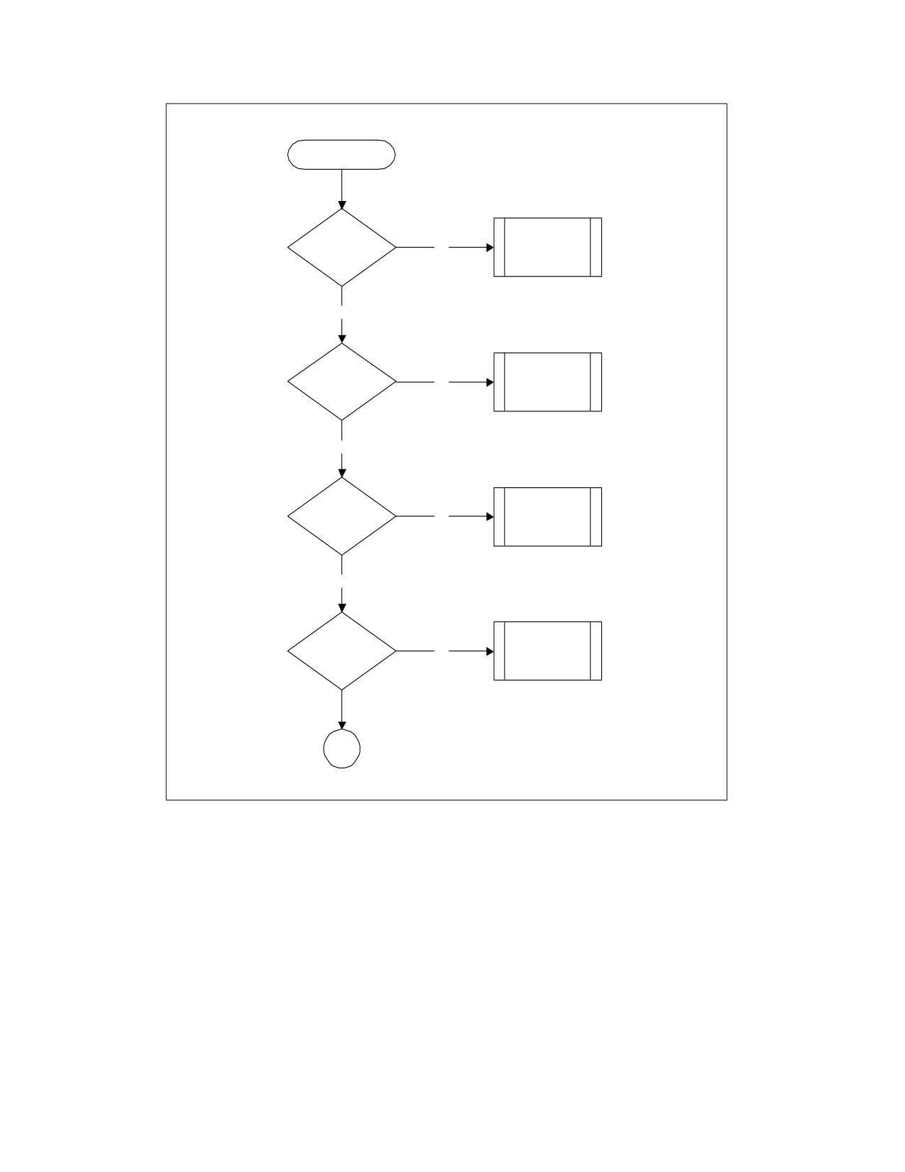
PROCESSOR MANAGEMENT AND INITIALIZATION
Write Microcode Update
Does Update Match A
Return
No
CPU_NOT_PRESENT
CPU in The System
Yes
Valid Update
Return
No
Header Version?
INVALID_HEADER
Yes
Return
Loader Revision Match
No
INVALID_HEADER
BIOS’s Loader?
Yes
Does Update
Return
Checksum Correctly?
No
INVALID_HEADER_CS
1
Figure 10-8. Microcode Update Write Operation Flow [1]
Vol. 3A
10-45
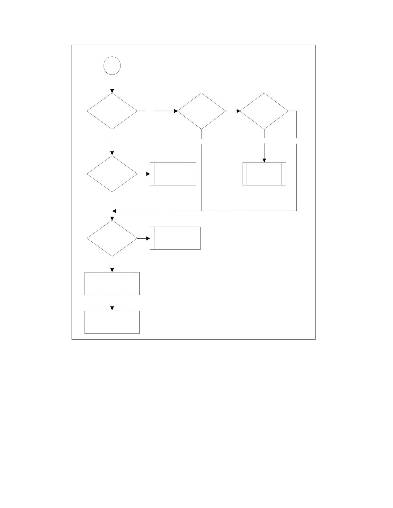
PROCESSOR MANAGEMENT AND INITIALIZATION
1
Replacement
Update Matching CPU
Space Available in
No
No
policy implemented?
Already In NVRAM?
NVRAM?
Yes
Yes
No
Yes
Update Revision Newer
Return
Return
No
Than NVRAM Update?
INVALID_REVISION
STORAGE_FULL
Yes
Update Pass
Return
Authenticity Test?
SECURITY_FAILURE
Yes
Update NMRAM Record
Return
SUCCESS
Figure 10-9. Microcode Update Write Operation Flow [2]
10.11.8.7 Function 02H-Microcode Update Control
This function enables loading of binary updates into the processor. Table 10-16 lists the parameters and return
codes for the function.
10-46
Vol. 3A

PROCESSOR MANAGEMENT AND INITIALIZATION
Table 10-16. Parameters for the Control Update Sub-function
Input
AX
Function Code
0D042H
BL
Sub-function
02H - Control update
BH
Task
See the description below.
CX
Scratch Pad1
Real mode segment of 64 KBytes of RAM block
DX
Scratch Pad2
Real mode segment of 64 KBytes of RAM block
SI
Scratch Pad3
Real mode segment of 64 KBytes of RAM block
SS:SP
Stack pointer
32 kilobytes of stack minimum
Output
CF
Carry Flag
Carry Set - Failure - AH contains status
Carry Clear - All return values valid.
AH
Return Code
Status of the call
AL
OEM Error
Additional OEM Information.
BL
Update Status
Either enable or disable indicator
Return Codes (see Table 10-19 for code definitions)
SUCCESS
Function completed successfully.
READ_FAILURE
A failure occurred because of the inability to read the storage device.
This control is provided on a global basis for all updates and processors. The caller can determine the current status
of update loading (enabled or disabled) without changing the state. The function does not allow the caller to disable
loading of binary updates, as this poses a security risk.
The caller specifies the requested operation by placing one of the values from Table 10-17 in the BH register. After
successfully completing this function, the BL register contains either the enable or the disable designator. Note that
if the function fails, the update status return value is undefined.
Table 10-17. Mnemonic Values
Mnemonic
Value
Meaning
Enable
1
Enable the Update loading at initialization time.
Query
2
Determine the current state of the update control without changing its status.
The READ_FAILURE error code returned by this function has meaning only if the control function is implemented in
the BIOS NVRAM. The state of this feature (enabled/disabled) can also be implemented using CMOS RAM bits
where READ failure errors cannot occur.
10.11.8.8 Function 03H-Read Microcode Update Data
This function reads a currently installed microcode update from the BIOS storage into a caller-provided RAM buffer.
Table 10-18 lists the parameters and return codes.
Table 10-18. Parameters for the Read Microcode Update Data Function
Input
AX
Function Code
0D042H
BL
Sub-function
03H - Read Update
ES:DI
Buffer Address
Real Mode pointer to the Intel Update structure that
will be written with the binary data
Vol. 3A
10-47

PROCESSOR MANAGEMENT AND INITIALIZATION
Table 10-18. Parameters for the Read Microcode Update Data Function (Contd.)
ECX
Scratch Pad1
Real Mode Segment address of 64 KBytes of RAM
Block (lower 16 bits)
ECX
Scratch Pad2
Real Mode Segment address of 64 KBytes of RAM
Block (upper 16 bits)
DX
Scratch Pad3
Real Mode Segment address of 64 KBytes of RAM
Block
SS:SP
Stack pointer
32 KBytes of Stack Minimum
SI
Update Number
This is the index number of the update block to be
read. This value is zero based and must be less than
the update count returned from the presence test
function.
Output
CF
Carry Flag
Carry Set
- Failure - AH contains Status
Carry Clear - All return values are
valid.
AH
Return Code
Status of the Call
AL
OEM Error
Additional OEM Information
Return Codes (see Table 10-19 for code definitions)
SUCCESS
The function completed successfully.
READ_FAILURE
There was a failure because of the inability to read the
storage device.
UPDATE_NUM_INVALID
Update number exceeds the maximum number of
update blocks implemented by the BIOS.
NOT_EMPTY
The specified update block is a subsequent block in use
to store a valid microcode update that spans multiple
blocks.
The specified block is not a header block and is not
empty.
The read function enables the caller to read any microcode update data that already exists in a BIOS and make
decisions about the addition of new updates. As a result of a successful call, the BIOS copies the microcode update
into the location pointed to by ES:DI, with the contents of all Update block(s) that are used to store the specified
microcode update.
If the specified block is not a header block, but does contain valid data from a microcode update that spans multiple
update blocks, then the BIOS must return Failure with the NOT_EMPTY error code in AH.
An update block is considered unused and available for storing a new update if its Header Version contains the
value 0FFFFFFFFH after return from this function call. The actual implementation of NVRAM storage management
is not specified here and is BIOS dependent. As an example, the actual data value used to represent an empty
block by the BIOS may be zero, rather than 0FFFFFFFFH. The BIOS is responsible for translating this information
into the header provided by this function.
10.11.8.9 Return Codes
After the call has been made, the return codes listed in Table 10-19 are available in the AH register.
10-48
Vol. 3A

PROCESSOR MANAGEMENT AND INITIALIZATION
Table 10-19. Return Code Definitions
Return Code
Value
Description
SUCCESS
00H
The function completed successfully.
NOT_IMPLEMENTED
86H
The function is not implemented.
ERASE_FAILURE
90H
A failure because of the inability to erase the storage device.
WRITE_FAILURE
91H
A failure because of the inability to write the storage device.
READ_FAILURE
92H
A failure because of the inability to read the storage device.
STORAGE_FULL
93H
The BIOS non-volatile storage area is unable to accommodate the update
because all available update blocks are filled with updates that are needed
for processors in the system.
CPU_NOT_PRESENT
94H
The processor stepping does not currently exist in the system.
INVALID_HEADER
95H
The update header contains a header or loader version that is not
recognized by the BIOS.
INVALID_HEADER_CS
96H
The update does not checksum correctly.
SECURITY_FAILURE
97H
The update was rejected by the processor.
INVALID_REVISION
98H
The same or more recent revision of the update exists in the storage device.
UPDATE_NUM_INVALID
99H
The update number exceeds the maximum number of update blocks
implemented by the BIOS.
NOT_EMPTY
9AH
The specified update block is a subsequent block in use to store a valid
microcode update that spans multiple blocks.
The specified block is not a header block and is not empty.
Vol. 3A
10-49
PROCESSOR MANAGEMENT AND INITIALIZATION
10-50
Vol. 3A
CHAPTER 11
ADVANCED PROGRAMMABLE INTERRUPT CONTROLLER (APIC)
The Advanced Programmable Interrupt Controller (APIC), referred to in the following sections as the local APIC,
was introduced into the IA-32 processors with the Pentium processor (see Section 23.27, “Advanced Program-
mable Interrupt Controller (APIC)”) and is included in the P6 family, Pentium 4, Intel Xeon processors, and other
more recent Intel 64 and IA-32 processor families (see Section 11.4.2, “Presence of the Local APIC”). The local
APIC performs two primary functions for the processor:
• It receives interrupts from the processor’s interrupt pins, from internal sources and from an external I/O APIC
(or other external interrupt controller). It sends these to the processor core for handling.
• In multiple processor (MP) systems, it sends and receives interprocessor interrupt (IPI) messages to and from
other logical processors on the system bus. IPI messages can be used to distribute interrupts among the
processors in the system or to execute system wide functions (such as, booting up processors or distributing
work among a group of processors).
The external I/O APIC is part of Intel’s system chipset. Its primary function is to receive external interrupt events
from the system and its associated I/O devices and relay them to the local APIC as interrupt messages. In MP
systems, the I/O APIC also provides a mechanism for distributing external interrupts to the local APICs of selected
processors or groups of processors on the system bus.
This chapter provides a description of the local APIC and its programming interface. It also provides an overview of
the interface between the local APIC and the I/O APIC. Contact Intel for detailed information about the I/O APIC.
When a local APIC has sent an interrupt to its processor core for handling, the processor uses the interrupt and
exception handling mechanism described in Chapter 6, “Interrupt and Exception Handling.” See Section 6.1, “Inter-
rupt and Exception Overview,” for an introduction to interrupt and exception handling.
11.1
LOCAL AND I/O APIC OVERVIEW
Each local APIC consists of a set of APIC registers (see Table 11-1) and associated hardware that control the
delivery of interrupts to the processor core and the generation of IPI messages. The APIC registers are memory
mapped and can be read and written to using the MOV instruction.
Local APICs can receive interrupts from the following sources:
• Locally connected I/O devices - These interrupts originate as an edge or level asserted by an I/O device
that is connected directly to the processor’s local interrupt pins (LINT0 and LINT1). The I/O devices may also
be connected to an 8259-type interrupt controller that is in turn connected to the processor through one of the
local interrupt pins.
• Externally connected I/O devices - These interrupts originate as an edge or level asserted by an I/O
device that is connected to the interrupt input pins of an I/O APIC. Interrupts are sent as I/O interrupt
messages from the I/O APIC to one or more of the processors in the system.
• Inter-processor interrupts (IPIs) - An Intel 64 or IA-32 processor can use the IPI mechanism to interrupt
another processor or group of processors on the system bus. IPIs are used for software self-interrupts,
interrupt forwarding, or preemptive scheduling.
• APIC timer generated interrupts - The local APIC timer can be programmed to send a local interrupt to its
associated processor when a programmed count is reached (see Section 11.5.4, “APIC Timer”).
• Performance monitoring counter interrupts - P6 family, Pentium 4, and Intel Xeon processors provide the
ability to send an interrupt to its associated processor when a performance-monitoring counter overflows (see
Section 20.6.3.5.8, “Generating an Interrupt on Overflow”).
• Thermal Sensor interrupts - Pentium 4 and Intel Xeon processors provide the ability to send an interrupt to
themselves when the internal thermal sensor has been tripped (see Section 15.8.2, “Thermal Monitor”).
• APIC internal error interrupts - When an error condition is recognized within the local APIC (such as an
attempt to access an unimplemented register), the APIC can be programmed to send an interrupt to its
associated processor (see Section 11.5.3, “Error Handling”).
Vol. 3A
11-1
ADVANCED PROGRAMMABLE INTERRUPT CONTROLLER (APIC)
Of these interrupt sources: the processor’s LINT0 and LINT1 pins, the APIC timer, the performance-monitoring
counters, the thermal sensor, and the internal APIC error detector are referred to as local interrupt sources.
Upon receiving a signal from a local interrupt source, the local APIC delivers the interrupt to the processor core
using an interrupt delivery protocol that has been set up through a group of APIC registers called the local vector
table or LVT (see Section 11.5.1, “Local Vector Table”). A separate entry is provided in the local vector table for
each local interrupt source, which allows a specific interrupt delivery protocol to be set up for each source. For
example, if the LINT1 pin is going to be used as an NMI pin, the LINT1 entry in the local vector table can be set up
to deliver an interrupt with vector number 2 (NMI interrupt) to the processor core.
The local APIC handles interrupts from the other two interrupt sources (externally connected I/O devices and IPIs)
through its IPI message handling facilities.
A processor can generate IPIs by programming the interrupt command register (ICR) in its local APIC (see Section
11.6.1, “Interrupt Command Register (ICR)”). The act of writing to the ICR causes an IPI message to be generated
and issued on the system bus (for Pentium 4 and Intel Xeon processors) or on the APIC bus (for Pentium and P6
family processors). See Section 11.2, “System Bus Vs. APIC Bus.”
IPIs can be sent to other processors in the system or to the originating processor (self-interrupts). When the target
processor receives an IPI message, its local APIC handles the message automatically (using information included
in the message such as vector number and trigger mode). See Section 11.6, “Issuing Interprocessor Interrupts,”
for a detailed explanation of the local APIC’s IPI message delivery and acceptance mechanism.
The local APIC can also receive interrupts from externally connected devices through the I/O APIC (see
Figure 11-1). The I/O APIC is responsible for receiving interrupts generated by system hardware and I/O devices
and forwarding them to the local APIC as interrupt messages.
Pentium 4 and
Pentium and P6
Intel Xeon Processors
Family Processors
Processor Core
Processor Core
Local APIC
Local APIC
Interrupt
Local
Interrupt
Local
Messages
Interrupts
Messages
Interrupts
Interrupt
System Bus
3-Wire APIC Bus
Messages
Bridge
External
I/O APIC
Interrupts
PCI
System Chipset
I/O APIC
External
Interrupts
System Chipset
Figure 11-1. Relationship of Local APIC and I/O APIC In Single-Processor Systems
Individual pins on the I/O APIC can be programmed to generate a specific interrupt vector when asserted. The I/O
APIC also has a “virtual wire mode” that allows it to communicate with a standard 8259A-style external interrupt
controller. Note that the local APIC can be disabled (see Section 11.4.3, “Enabling or Disabling the Local APIC”).
This allows an associated processor core to receive interrupts directly from an 8259A interrupt controller.
Both the local APIC and the I/O APIC are designed to operate in MP systems (see Figures 11-2 and 11-3). Each local
APIC handles interrupts from the I/O APIC, IPIs from processors on the system bus, and self-generated interrupts.
Interrupts can also be delivered to the individual processors through the local interrupt pins; however, this mecha-
nism is commonly not used in MP systems.
11-2
Vol. 3A
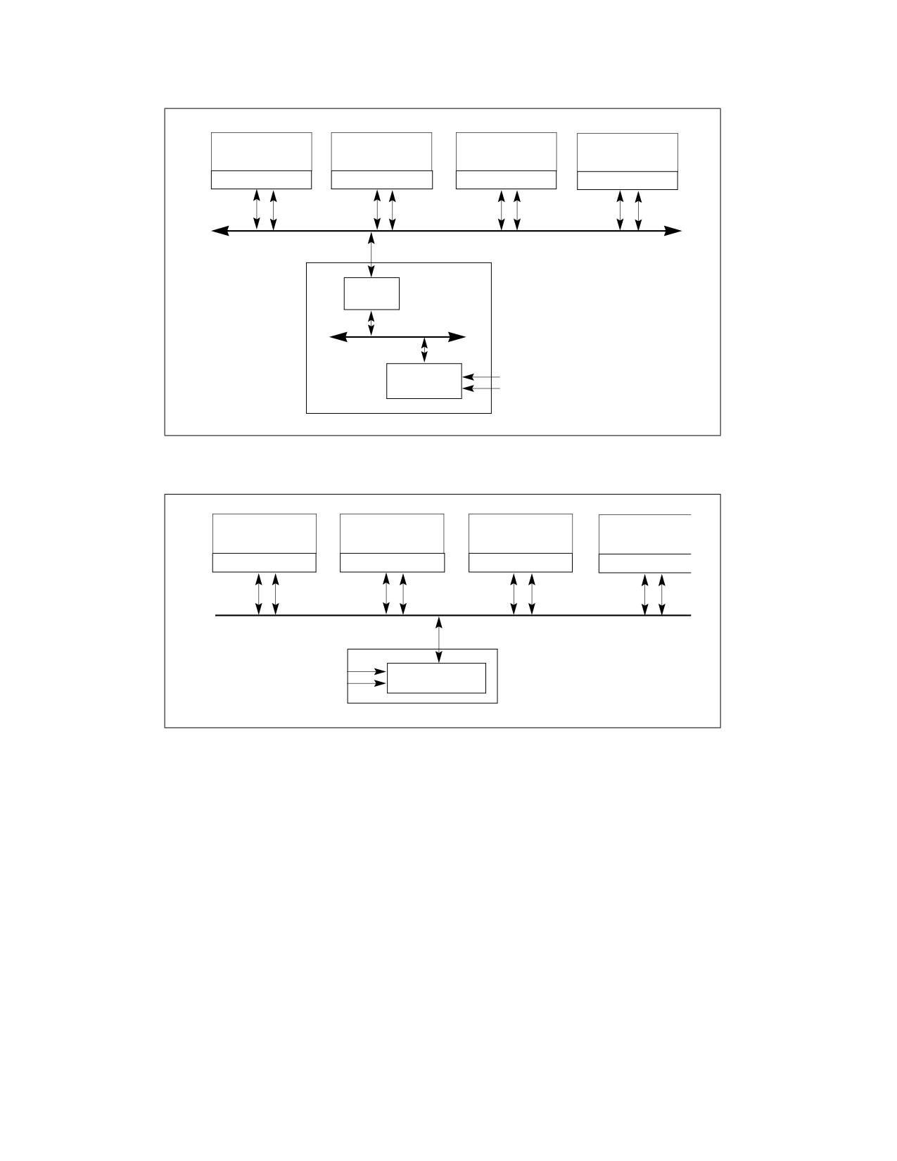
ADVANCED PROGRAMMABLE INTERRUPT CONTROLLER (APIC)
Processor #1
Processor #2
Processor #3
Processor #3
CPU
CPU
CPU
CPU
Local APIC
Local APIC
Local APIC
Local APIC
Interrupt
Interrupt
Interrupt
Interrupt
IPIs
IPIs
IPIs
IPIs
Messages
Messages
Messages
Messages
Processor System Bus
Interrupt
Messages
Bridge
PCI
I/O APIC
External
Interrupts
System Chipset
Figure 11-2. Local APICs and I/O APIC When Intel Xeon Processors Are Used in Multiple-Processor Systems
Processor #1
Processor #2
Processor #3
Processor #4
CPU
CPU
CPU
CPU
Local APIC
Local APIC
Local APIC
Local APIC
Interrupt
IPIs
Interrupt
IPIs
Interrupt
IPIs
Interrupt
IPIs
Messages
Messages
Messages
Messages
Interrupt
3-wire APIC Bus
Messages
External
I/O APIC
Interrupts
System Chipset
Figure 11-3. Local APICs and I/O APIC When P6 Family Processors Are Used in Multiple-Processor Systems
The IPI mechanism is typically used in MP systems to send fixed interrupts (interrupts for a specific vector number)
and special-purpose interrupts to processors on the system bus. For example, a local APIC can use an IPI to
forward a fixed interrupt to another processor for servicing. Special-purpose IPIs (including NMI, INIT, SMI, and
SIPI IPIs) allow one or more processors on the system bus to perform system-wide boot-up and control functions.
The following sections focus on the local APIC and its implementation in the Pentium 4, Intel Xeon, and P6 family
processors. In these sections, the terms “local APIC” and “I/O APIC” refer to local and I/O APICs used with the P6
family processors and to local and I/O xAPICs used with the Pentium 4 and Intel Xeon processors (see Section
11.3, “The Intel® 82489DX External APIC, the APIC, the xAPIC, and the X2APIC”).
11.2
SYSTEM BUS VS. APIC BUS
For the P6 family and Pentium processors, the I/O APIC and local APICs communicate through the 3-wire inter-
APIC bus (see Figure 11-3). Local APICs also use the APIC bus to send and receive IPIs. The APIC bus and its
messages are invisible to software and are not classed as architectural.
Vol. 3A
11-3
ADVANCED PROGRAMMABLE INTERRUPT CONTROLLER (APIC)
Beginning with the Pentium 4 and Intel Xeon processors, the I/O APIC and local APICs (using the xAPIC architec-
ture) communicate through the system bus (see Figure 11-2). The I/O APIC sends interrupt requests to the
processors on the system bus through bridge hardware that is part of the Intel chipset. The bridge hardware gener-
ates the interrupt messages that go to the local APICs. IPIs between local APICs are transmitted directly on the
system bus.
11.3
THE INTEL® 82489DX EXTERNAL APIC, THE APIC, THE XAPIC, AND THE
X2APIC
The local APIC in the P6 family and Pentium processors is an architectural subset of the Intel® 82489DX external
APIC. See Section 23.27.1, “Software Visible Differences Between the Local APIC and the 82489DX.”
The APIC architecture used in the Pentium 4 and Intel Xeon processors (called the xAPIC architecture) is an exten-
sion of the APIC architecture found in the P6 family processors. The primary difference between the APIC and
xAPIC architectures is that with the xAPIC architecture, the local APICs and the I/O APIC communicate through the
system bus. With the APIC architecture, they communication through the APIC bus (see Section 11.2, “System Bus
Vs. APIC Bus”). Also, some APIC architectural features have been extended and/or modified in the xAPIC architec-
ture. These extensions and modifications are described in Section 11.4 through Section 11.10.
The basic operating mode of the xAPIC is xAPIC mode. The x2APIC architecture is an extension of the xAPIC
architecture, primarily to increase processor addressability. The x2APIC architecture provides backward compati-
bility to the xAPIC architecture and forward extendability for future Intel platform innovations. These extensions
and modifications are supported by a new mode of execution (x2APIC mode) are detailed in Section 11.12.
11.4
LOCAL APIC
The following sections describe the architecture of the local APIC and how to detect it, identify it, and determine its
status. Descriptions of how to program the local APIC are given in Section 11.5.1, “Local Vector Table,” and Section
11.6.1, “Interrupt Command Register (ICR).”
11.4.1 The Local APIC Block Diagram
Figure 11-4 gives a functional block diagram for the local APIC. Software interacts with the local APIC by reading
and writing its registers. APIC registers are memory-mapped to a 4-KByte region of the processor’s physical
address space with an initial starting address of FEE00000H. For correct APIC operation, this address space must
be mapped to an area of memory that has been designated as strong uncacheable (UC). See Section 12.3,
“Methods of Caching Available.”
In MP system configurations, the APIC registers for Intel 64 or IA-32 processors on the system bus are initially
mapped to the same 4-KByte region of the physical address space. Software has the option of changing initial
mapping to a different 4-KByte region for all the local APICs or of mapping the APIC registers for each local APIC to
its own 4-KByte region. Section 11.4.5, “Relocating the Local APIC Registers,” describes how to relocate the base
address for APIC registers.
On processors supporting x2APIC architecture (indicated by CPUID.01H:ECX[21] = 1), the local APIC supports
operation both in xAPIC mode and (if enabled by software) in x2APIC mode. x2APIC mode provides extended
processor addressability (see Section 11.12).
NOTE
For P6 family, Pentium 4, and Intel Xeon processors, the APIC handles all memory accesses to
addresses within the 4-KByte APIC register space internally and no external bus cycles are
produced. For the Pentium processors with an on-chip APIC, bus cycles are produced for accesses
to the APIC register space. Thus, for software intended to run on Pentium processors, system
software should explicitly not map the APIC register space to regular system memory. Doing so can
result in an invalid opcode exception (#UD) being generated or unpredictable execution.
11-4
Vol. 3A
ADVANCED PROGRAMMABLE INTERRUPT CONTROLLER (APIC)
Version Register
EOI Register
Timer
Task Priority Register
Current Count
Register
INTA
From
Initial Count
Processor Priority
CPU
Register
Register
Core
Divide Configuration
Register
INTR To
Prioritizer
Local Vector Table
CPU
EXTINT
Core
Timer
In-Service Register (ISR)
Local
LINT0/1
Interrupt Request Register (IRR)
Interrupts 0,1
Perf. Mon.
Performance
Trigger Mode Register (TMR)
(Internal
Monitoring Counters1/
Interrupt)
Intel Processor Trace
Vec[3:0]
Register
Thermal
& TMR Bit
Select
Sensor
Thermal Sensor2
(Internal
Arb. ID
Vecter
Interrupt)
Error
Register4
Decode
Error Status
Register
Local
Acceptance
Interrupts
Logic
Dest. Mode
& Vector
APIC ID
To
Register
Protocol
CPU
Logical Destination
Translation Logic
INIT
Core
Register
NMI
SMI
Destination Format
Register
Interrupt Command
Register (ICR)
Spurious Vector Register
Processor System Bus3
1. Introduced in P6 family processors.
2. Introduced in the Pentium 4 and Intel Xeon processors.
3. Three-wire APIC bus in P6 family and Pentium processors.
4. Not implemented in Pentium 4 and Intel Xeon processors.
Figure 11-4. Local APIC Structure
Table 11-1 shows how the APIC registers are mapped into the 4-KByte APIC register space. Registers are 32 bits,
64 bits, or 256 bits in width; all are aligned on 128-bit boundaries. All 32-bit registers should be accessed using
128-bit aligned 32-bit loads or stores. Some processors may support loads and stores of less than 32 bits to some
of the APIC registers. This is model specific behavior and is not guaranteed to work on all processors. Any
FP/MMX/SSE access to an APIC register, or any access that touches bytes 4 through 15 of an APIC register may
cause undefined behavior and must not be executed. This undefined behavior could include hangs, incorrect results
or unexpected exceptions, including machine checks, and may vary between implementations. Wider registers
(64-bit or 256-bit) must be accessed using multiple 32-bit loads or stores, with all accesses being 128-bit aligned.
The local APIC registers listed in Table 11-1 are not MSRs. The only MSR associated with the programming of the
local APIC is the IA32_APIC_BASE MSR (see Section 11.4.3, “Enabling or Disabling the Local APIC”).
NOTE
In processors based on Nehalem1 microarchitecture, the Local APIC ID Register is no longer
Read/Write; it is Read Only.
Vol. 3A
11-5

ADVANCED PROGRAMMABLE INTERRUPT CONTROLLER (APIC)
Table 11-1. Local APIC Register Address Map
Address
Register Name
Software Read/Write
FEE0 0000H
Reserved
FEE0 0010H
Reserved
FEE0 0020H
Local APIC ID Register
Read/Write.
FEE0 0030H
Local APIC Version Register
Read Only.
FEE0 0040H
Reserved
FEE0 0050H
Reserved
FEE0 0060H
Reserved
FEE0 0070H
Reserved
FEE0 0080H
Task Priority Register (TPR)
Read/Write.
FEE0 0090H
Arbitration Priority Register1 (APR)
Read Only.
FEE0 00A0H
Processor Priority Register (PPR)
Read Only.
FEE0 00B0H
EOI Register
Write Only.
FEE0 00C0H
Remote Read Register1 (RRD)
Read Only
FEE0 00D0H
Logical Destination Register
Read/Write.
FEE0 00E0H
Destination Format Register
Read/Write (see Section
11.6.2.2).
FEE0 00F0H
Spurious Interrupt Vector Register
Read/Write (see Section 11.9.
FEE0 0100H
In-Service Register (ISR); bits 31:0
Read Only.
FEE0 0110H
In-Service Register (ISR); bits 63:32
Read Only.
FEE0 0120H
In-Service Register (ISR); bits 95:64
Read Only.
FEE0 0130H
In-Service Register (ISR); bits 127:96
Read Only.
FEE0 0140H
In-Service Register (ISR); bits 159:128
Read Only.
FEE0 0150H
In-Service Register (ISR); bits 191:160
Read Only.
FEE0 0160H
In-Service Register (ISR); bits 223:192
Read Only.
FEE0 0170H
In-Service Register (ISR); bits 255:224
Read Only.
FEE0 0180H
Trigger Mode Register (TMR); bits 31:0
Read Only.
FEE0 0190H
Trigger Mode Register (TMR); bits 63:32
Read Only.
FEE0 01A0H
Trigger Mode Register (TMR); bits 95:64
Read Only.
FEE0 01B0H
Trigger Mode Register (TMR); bits 127:96
Read Only.
FEE0 01C0H
Trigger Mode Register (TMR); bits 159:128
Read Only.
FEE0 01D0H
Trigger Mode Register (TMR); bits 191:160
Read Only.
FEE0 01E0H
Trigger Mode Register (TMR); bits 223:192
Read Only.
FEE0 01F0H
Trigger Mode Register (TMR); bits 255:224
Read Only.
FEE0 0200H
Interrupt Request Register (IRR); bits 31:0
Read Only.
FEE0 0210H
Interrupt Request Register (IRR); bits 63:32
Read Only.
FEE0 0220H
Interrupt Request Register (IRR); bits 95:64
Read Only.
1. See Table 2-1, “CPUID Signature Values of DisplayFamily_DisplayModel,” on page 1, and Section 2.8, “MSRs In Processors Based on
Nehalem Microarchitecture,” of the Intel® 64 and IA-32 Architectures Software Developer’s Manual, Volume 4, to determine which
processors are based on Nehalem microarchitecture.
11-6
Vol. 3A

ADVANCED PROGRAMMABLE INTERRUPT CONTROLLER (APIC)
Table 11-1. Local APIC Register Address Map (Contd.)
Address
Register Name
Software Read/Write
FEE0 0230H
Interrupt Request Register (IRR); bits 127:96
Read Only.
FEE0 0240H
Interrupt Request Register (IRR); bits 159:128
Read Only.
FEE0 0250H
Interrupt Request Register (IRR); bits 191:160
Read Only.
FEE0 0260H
Interrupt Request Register (IRR); bits 223:192
Read Only.
FEE0 0270H
Interrupt Request Register (IRR); bits 255:224
Read Only.
FEE0 0280H
Error Status Register
Write/Read; see Section
11.5.3.
FEE0 0290H through
Reserved
FEE0 02E0H
FEE0 02F0H
LVT Corrected Machine Check Interrupt (CMCI) Register
Read/Write.
FEE0 0300H
Interrupt Command Register (ICR); bits 0-31
Read/Write.
FEE0 0310H
Interrupt Command Register (ICR); bits 32-63
Read/Write.
FEE0 0320H
LVT Timer Register
Read/Write.
FEE0 0330H
LVT Thermal Sensor Register2
Read/Write.
FEE0 0340H
LVT Performance Monitoring Counters Register3
Read/Write.
FEE0 0350H
LVT LINT0 Register
Read/Write.
FEE0 0360H
LVT LINT1 Register
Read/Write.
FEE0 0370H
LVT Error Register
Read/Write.
FEE0 0380H
Initial Count Register (for Timer)
Read/Write.
FEE0 0390H
Current Count Register (for Timer)
Read Only.
FEE0 03A0H through
Reserved
FEE0 03D0H
FEE0 03E0H
Divide Configuration Register (for Timer)
Read/Write.
FEE0 03F0H
Reserved
NOTES:
1. Not supported in the Pentium 4 and Intel Xeon processors. The Illegal Register Access bit (7) of the ESR will not be set when writ-
ing to these registers.
2. Introduced in the Pentium 4 and Intel Xeon processors. This APIC register and its associated function are implementation depen-
dent and may not be present in future IA-32 or Intel 64 processors.
3. Introduced in the Pentium Pro processor. This APIC register and its associated function are implementation dependent and may not
be present in future IA-32 or Intel 64 processors.
11.4.2 Presence of the Local APIC
Beginning with the P6 family processors, the presence or absence of an on-chip local APIC can be detected using
the CPUID instruction. When the CPUID instruction is executed with a source operand of 1 in the EAX register, bit 9
of the CPUID feature flags returned in the EDX register indicates the presence (set) or absence (clear) of a local
APIC.
11.4.3 Enabling or Disabling the Local APIC
The local APIC can be enabled or disabled in either of two ways:
1. Using the APIC global enable/disable flag in the IA32_APIC_BASE MSR (MSR address 1BH; see Figure 11-5):
Vol. 3A
11-7
ADVANCED PROGRAMMABLE INTERRUPT CONTROLLER (APIC)
- When IA32_APIC_BASE[11] is 0, the processor is functionally equivalent to an IA-32 processor without an
on-chip APIC. The CPUID feature flag for the APIC (see Section 11.4.2, “Presence of the Local APIC”) is also
set to 0.
- When IA32_APIC_BASE[11] is set to 0, processor APICs based on the 3-wire APIC bus cannot be generally
re-enabled until a system hardware reset. The 3-wire bus loses track of arbitration that would be necessary
for complete re-enabling. Certain APIC functionality can be enabled (for example: performance and
thermal monitoring interrupt generation).
- For processors that use Front Side Bus (FSB) delivery of interrupts, software may disable or enable the
APIC by setting and resetting IA32_APIC_BASE[11]. A hardware reset is not required to re-start APIC
functionality, if software guarantees no interrupt will be sent to the APIC as IA32_APIC_BASE[11] is
cleared.
- When IA32_APIC_BASE[11] is set to 0, prior initialization to the APIC may be lost and the APIC may return
to the state described in Section 11.4.7.1, “Local APIC State After Power-Up or Reset.”
2. Using the APIC software enable/disable flag in the spurious-interrupt vector register (see Figure 11-23):
- If IA32_APIC_BASE[11] is 1, software can temporarily disable a local APIC at any time by clearing the APIC
software enable/disable flag in the spurious-interrupt vector register (see Figure 11-23). The state of the
local APIC when in this software-disabled state is described in Section 11.4.7.2, “Local APIC State After It
Has Been Software Disabled.”
- When the local APIC is in the software-disabled state, it can be re-enabled at any time by setting the APIC
software enable/disable flag to 1.
For the Pentium processor, the APICEN pin (which is shared with the PICD1 pin) is used during power-up or reset
to disable the local APIC.
Note that each entry in the LVT has a mask bit that can be used to inhibit interrupts from being delivered to the
processor from selected local interrupt sources (the LINT0 and LINT1 pins, the APIC timer, the performance-moni-
toring counters, Intel® Processor Trace, the thermal sensor, and/or the internal APIC error detector).
11.4.4 Local APIC Status and Location
The status and location of the local APIC are contained in the IA32_APIC_BASE MSR (see Figure 11-5). MSR bit
functions are described below:
• BSP flag, bit 8 ⎯ Indicates if the processor is the bootstrap processor (BSP). See Section 9.4, “Multiple-
Processor (MP) Initialization.” Following a power-up or reset, this flag is set to 1 for the processor selected as
the BSP and set to 0 for the remaining processors (APs).
• APIC Global Enable flag, bit 11 ⎯ Enables or disables the local APIC (see Section 11.4.3, “Enabling or
Disabling the Local APIC”). This flag is available in the Pentium 4, Intel Xeon, and P6 family processors. It is not
guaranteed to be available or available at the same location in future Intel 64 or IA-32 processors.
• APIC Base field, bits 12 through 35 ⎯ Specifies the base address of the APIC registers. This 24-bit value is
extended by 12 bits at the low end to form the base address. This automatically aligns the address on a 4-KByte
boundary. Following a power-up or reset, the field is set to FEE0 0000H.
• Bits 0 through 7, bits 9 and 10, and bits MAXPHYADDR1 through 63 in the IA32_APIC_BASE MSR are reserved.
1. The MAXPHYADDR is 36 bits for processors that do not support CPUID leaf 80000008H, or indicated by
CPUID.80000008H:EAX[bits 7:0] for processors that support CPUID leaf 80000008H.
11-8
Vol. 3A