OMRON NB-Designer OPERATION MANUAL (NB-series, 2020) - page 19
Appendices
A-2
NB-Designer Function List
Items
Descriptions of Function
Parts
Bit Button
Operations such as the touch input allow the specified bit address turned
ON/OFF.
Bit Lamp
Indicates the specified ON/OFF state of one bit address.
Bit Switch
Operations such as touch input allow the specified bit address turned
ON/OFF. Specify the Read/Write addresses separately to operate them as
the lamp.
Command Button
Function Component performs several processing such as transmission of
constant value.
Word Lamp
Function Component switches the display status according to the change
with value of the communications address.
Word Switch
Function Component performs increase and decrease of the value or
transmission of the value selected from the list.
XY Graph
Describing a continuum from the value of the communications addresses as
each point of coordinates in the component area. The shape can be modified
dynamically.
Moving
Describing the vector graphics or the bit map from the value of the
Component
communications addresses as point of coordinates. The shape can be
modified dynamically.
Animation
Draw the component with the specified track in the PT, and this position is
determined by the value of the preset path and the communication
addresses.
Number Input
Display the specified value of the communication address. Also Entering
number by pop-up keyboard and pressing [ENTER] allow the communication
address modified.
Number Display
Display the value of the specified communication address.
Text Input
Set the value of the specified communication address to text string data. The
input data is saved to a consecutive memory with the “Read Address” as the
first address.
Text Display
Display the value of the specified communication address as text string.
Level Meter
Display the value of the specified communications address in a bar chart
percentage style according to the set maximum and minimum values.
Analog Meter
Display the value of the specified communication address by means of a
Analog Meter diagram.
Indirect Screen
Display the screen of the specified screen No. in pop-up screen.
Direct Screen
Display the specified screen in pop-up screen.
Alarm
Display the occurred alarm information in the specified area. The content
displayed by the Alarm Display component is the same as that displayed by
the Alarm component.
Data Log
Obtain the values of periodically specified communications address and
display them in the graphic chart. The background communication still
continues to do when the current screen where the Data Log locates is
closed. Even after the switching the screen in which the Data Log component
located to another screen, if the screen in which Data Log component
located is refreshed, the sampling data which was obtained until switching
the screen can be displayed.
Recipe
Used to transfer the data from the recipe memory of PT to PLC or PLC data
to the PT Recipe memory.
Oscillograph
The Oscillograph functions similarly to the Data Log. But the data sampling
of the Oscillograph is valid only during the screen in which the Oscillograph
is located is displayed, which means that each time the screen is switched,
the sampling data will be deleted and a new sampling will be started.
A-6
Appendices
Items
Descriptions of Function
Parts
Scroll Bar
Move the slider to modify the value of the specified communications address.
Event
Used to make the event information logged in “Event Information” and
meeting the current triggering conditions displayed.
Note Book
Used to modify or display the value of the specified communications
address. The input data is saved to a consecutive memory with the “Read
Address” as the first address.
Word Neon Lamp
Used to display the label contents in loopy moving way, and it supports the
label contents corresponding to 256 (max.) states in the loopy-moving way.
Bit Neon Lamp
Used to display the label contents in loopy moving way, and it supports the
label contents corresponding to State 0 and State 1 in the loopy-moving way.
Touch Trigger
This function allows the multiple components operated all at once. When the
communications addresses specified to the Touch Trigger component are
satisfied to the trigger conditions, the components placed in the valid area for
the Touch Trigger component can be triggered to act.
Table
Used to make the selection type of “Select by row”, “Select by column” and
“Select by cell”. The user can set the “Row”, “Column”, “Select Color”,
“Background Color”, “Border Color”, and write the selected Row No. and
Column No. into the specified communication address.
Data History
Read the consecutive addresses of the memory periodically with the top of
the specified communications address, and display in the table format.
Event History
It can be used to search or display the event history information, which is
Display
recorded in the “Event Setting” database and whose current state meets the
triggering conditions, in the table form. And this component works only
together with the external memory.
Operation Log
It can be used to record or display the PT operations in the table form. The
operation log will be stored into the external memory in CSV format. This
component works only together with the external memory.
Function
Scale
Draw the scale for the shapes such as portrait, landscape, arc, and circle.
Parts
Function Key
Used to provide functions such as “Switch Screens”, “Keyboard Function”,
“Execute Macro”, “Touch Calibration”, “Clear Event” and “Notepad” etc. The
function key cannot be controlled by the communication address. so the
execution of specified function needs to be activated by touching this
component.
Alarm Display
When the bit address specified with [Alarm Setting] matched to the trigger
condition, display the specified message. The message will be displayed in
loopy-moving way at the site where the alarm display is placed. The alarm
information will continue to scroll until this bit address is switched to the non-
alarm state.
Timer
When the specified duration is passed, other functions such as the Macro
execution, writing the value, or the data transmission are performed.
Bitmap
Used to call and display the bg-form graphics in the system graphics library
or the graphics library in project file window. The graphics in the formats
such as .jpg, .bmp, .gif, .png can be imported into the bitmap and displayed.
Vector Graphics
Call and display the graphics in vg format in system graphics library
displayed or project file window. Vector Graphics can be generated from the
file in “.JPG, .BMP, .GIF, or .PNG” formats.
Notepad
Draw the texts or graphics manually and freely in the specified area.
Data Transmission
Transmitting the value of the specified communication address to the other
communications address. Data Transmission can be triggered by the manual
touching method or the state change of the specified address.
FreePlotting
Draw the graphics with the pixel based on the consecutive data stored in the
specified communications addresses.
A-7
Appendices
Items
Descriptions of Function
Function
Date/Time
Used to display the value of the RTC clock inside the PT in the set format.
Parts
Indirect Shape
Modifying the specified communications addresses allows the specifying
rectangle, ellipse, location and size of the lines to draw the shape.
User Information
Used to display the related information of the current login user in the table
form.
Multifunction
Used to incorporate the Bit Button component and Command Button
component into one component, thus making the user realize the Bit Set and
Word Set operations through only one key.
Event Display
Display the event information with [Event Setting] matching to the specified
trigger condition.
File List
The File List is used to display the file information of the external memory.
This component is divided into three parts: the left part displays the
information on the folder under the current folder, the upper-right part
displays the information on the file under the current folder, and the lower-
right part displays the PT information on the selected project file.
Project
Text Library
Specify the necessary text strings in advance, thus preventing the label with
Database
the same text from being input frequently.
Variable Table
It is a useful address library, which prevents the inconvenience resulting from
repeated input of address.
Alarm Setting
Specifying the message displayed in [Alarm] or [Alarm Display] and the bit
address and the trigger conditions applied to the trigger. If the bit address
registered to [Alarm Setting] matches the specified trigger condition, the
registered message will be displayed.
Event Setting
Specifying the function operated with the message displayed in [Event] or
[Event Display], the communications addressed which should be the trigger,
and the trigger condition. If the bit address or word address registered to the
[Event Setting] are matched the specified trigger condition, the registered
function can be operated or the registered message can be displayed.
PLC Control
Specify the communication address allocated to the specific functions as
follows. It is available to select among the screen switching, writing the data
(the current base screen) in the PLC, general PLC controlling, turning OFF
the back light, and turning ON the back light and others.
Screen
Base Screen
It is the general screen.
Type
Common Sheet
There is only 1 Common Sheet, which can be set to above or under the Base
Screen.
The maximum number of Base Screen ejected in 1 Common Sheet is up to
16.
Menu Screen
There is only 1 Menu Screen, which will appear only after “Menu” is touched.
Sheet Screen
Up to 3 Sheet Screens can be set for 1 Base Screen.
Pop-up Screen
The types are “Tracking”, “Modal”, “Clipping” and “Fixed”.
It can be displayed normally or in the top layer.
The maximum number of Pop-up Screen ejected in 1 Base Screen is up to
16.
Direct Screen
Up to 16 Direct Screens can be displayed simultaneously in 1 Base Screen.
It is controlled by the bit.
Indirect Screen
Up to 16 Indirect Screens can be displayed simultaneously in 1 Base Screen.
It is controlled by word.
Screen Property
Security level of the screen, screen attribute, background color, transparency
rate, width and color of frame, location to place screen, size of screen (width
and height), sheet screen allocated to screen (three screens at max.), type of
pop-up used as pop-up can be specified.
A-8
Appendices
Items
Descriptions of Function
Screen
Maximum Screen
It is up to 32768.
Number
Number
Screen No.
It includes 0 and 10 to 32767 (Base Screens)
1: Common Sheet (Default)
2: Menu Screen (Default)
3: NUM Keyboard (Default)
4: ASCII Keyboard (Default)
5: File List Screen (Reserved by system)
6: Password Screen (Reserved by system)
7: Confirmation Screen (Default)
8: HEX Keyboard (Default)
9: Login Screen (Default)
Screen Switching Method
The function of switching screen with [Function Key] allows switching the
displayed screen to optional base screen, common sheet screen, menu
screen, or pop-up screen.
Entering the optional screen No. to the communications address specified to
the function of switching screen with [PLC Control] allows switching the
screen to the screen with the entered screen No.
Macro Function
The function to create the simple original program by the user and to execute
it. The user can add the functions such a arithmetical operations or
discriminant of the conditions which are not be supported by the basic
functions of the NB-Designer. Using the Macro function, the user also
convert the display processing in the screen or the data processing used to
be performed in the PLC. This function allows the PC loading reduced. The
Macro of the NB-Designer conforms to C Language (ANSI C89).
Internal
LB
Refers to the local bit address of PT, which can’t be saved when power is
Address
OFF.
inside PT
RB
Refers to the absolute address of bit address saved in the recipe data that is
stored in the flash memory, even when the power turns OFF, the data can be
retained. Even if the battery is dead in PT, the data stored in the recipe
memory will not be lost.
RBI
Refers to the index address of bit address saved in the recipe data that is
stored in the flash memory, even when the power turns OFF, the data can be
retained. Even if the battery is dead in PT, the data stored in the recipe
memory will not be lost.
LW.B
Refers to the bit address corresponding to the local word address of PT,
which can’t be retained when the power is OFF.
FRB
Refers to the bit address to be stored in the flash memory, even when the PT
turns OFF, the stored data can be retained. When the battery is dead in PT,
the data saved in flash memory will not be affected.
FRBI
Refers to the index address of bit address saved in flash memory, which can
be retained when the power of PT turns OFF. When the battery is dead in
PT, the data saved in flash memory will not be affected.
LW
Refers to the local word address of PT, which can’t be retained when power
is OFF.
RW
Refers to the absolute address saved in the recipe data that is stored in the
flash memory, which can be retained when the power of PT turns OFF. Even
if the battery is dead in PT, the data stored in the recipe memory will not be
lost.
RWI
Refers to the index address saved in the recipe data that is stored in the
flash memory, which can be saved when the power is OFF. Even if the
battery is dead in PT, the stored data in the flash memory can be retained.
FRW
Refers to the word address stored in the flash memory, which can be
retained when the power of PT turns OFF. When the battery is dead in PT,
the data saved in flash memory will not be affected.
A-9
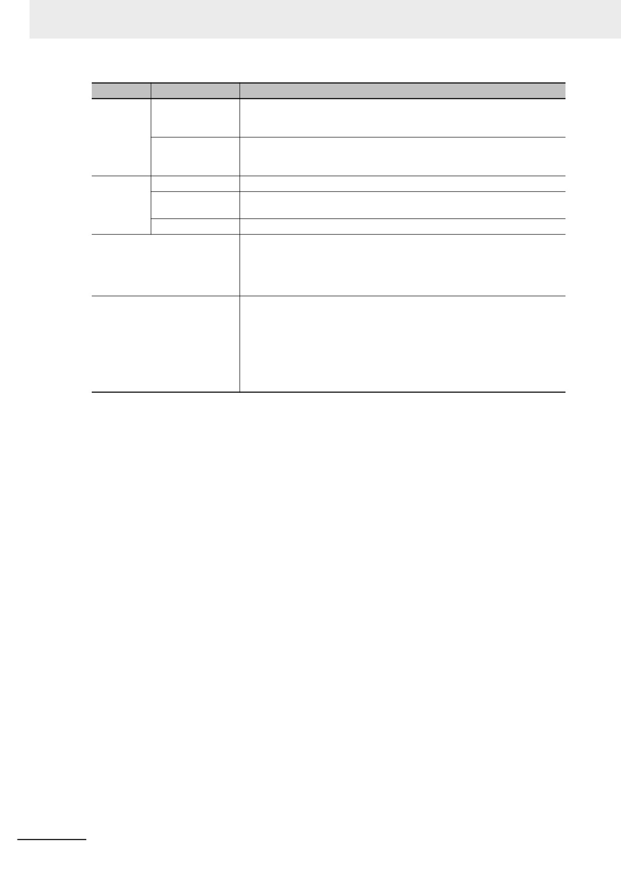
Appendices
Items
Descriptions of Function
Internal
FRWI
Refers to the index address of word address saved in flash memory, which
Address
can be retained when the power of PT turns OFF. When the battery is dead
inside PT
in PT, the data saved in flash memory will not be affected.
ERW
Refers to the word address stored in the external memory, which can be
retained when the power of PT turns OFF. When the battery is dead in PT,
the data saved in external memory will not be affected.
File Formats
.rcp
It is the file format which is used by PT device.
Supported by
.frp
It is the file format of Recipe data saved and used in the flash memory of the
RecipeEditor
NB.
.csv
It can be imported/exported with Microsoft Excel or others.
Security Level
The security level is classified into 16 levels (0 to 15). The optional
passwords can be specified every one pasword for each level wit eight digits.
And the greater the level number, the higher the level. 15-level is the highest
and 0-level is the lowest. When the security level is 0, password cannot be
specified. The number of the security level is specified to “3” by default.
User Permission
User permission can be specified for 32 users at max. Also all the 32 kinds of
user permission can be specified for each user. The same user permission
can be specified to the multiple different users. The addition and deletion of
user or the modification of user permission settings can be performed on NB
units using system memory. The default valid time of user permission is 10
minutes. When 10 minutes passed after the login, this user permission will
be automatically cancelled, and the operation permission can be obtained by
inputting the password again.
Note Data saving into a flash memory such as RB/RW and FRB/FRW or an external memory such as ERW is per-
formed in accordance with CPU's processing load.
If turning off the power before saving, you may lose data because data is not instantly saved.
A-10
Appendices
A-3
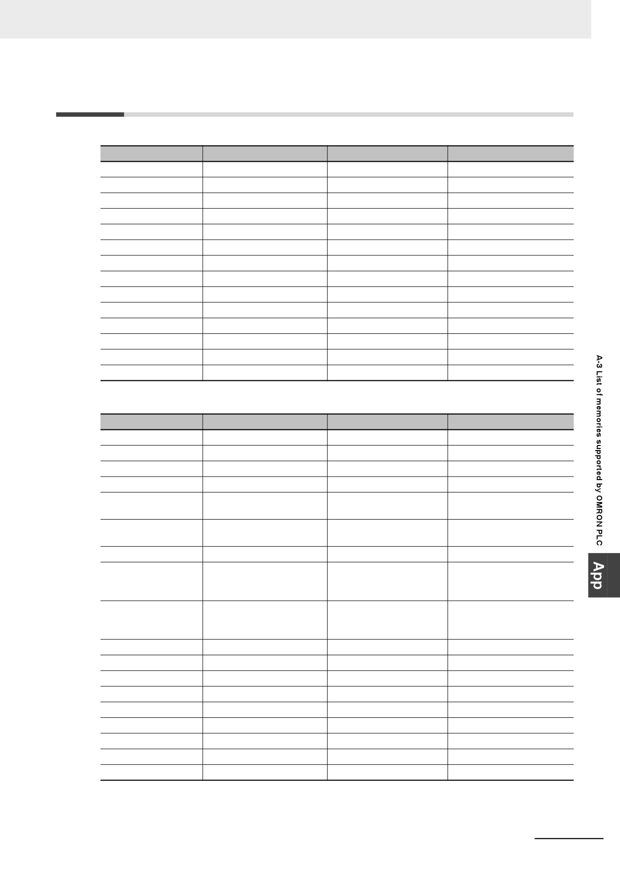
List of memories supported by OMRON PLC
z Omron C Series
Device
Bit Address
Word Address
Format
Counter (Completion Flag)
C_FLAG 0-511
------
DDD
Timer (Completion Flag)
T_FLAG 0-511
------
DDD
Holding Area
H_bit 00.00-99.15
------
DD.DD
Data Area
D_bit 0000.00-6655.15
------
DDDD.DD
Link Area
LR_bit 00.00-63.15
------
DD.DD
Auxiliary Area
A_bit 00.00-27.15
------
DD.DD
CIO Area
CIO_IR_bit 000.00-511.15
------
DDD.DD
Counter Area
------
C 000-511
DDD
Timer Area
------
T 000-511
DDD
Holding Area
------
H 00-99
DD
Data Area
------
D 0000-6655
DDDD
Link Area
------
LR 00-63
DD
Auxiliary Area
------
A 0-27
DD
CIO Area
------
CIO_IR_word 000-511
DDD
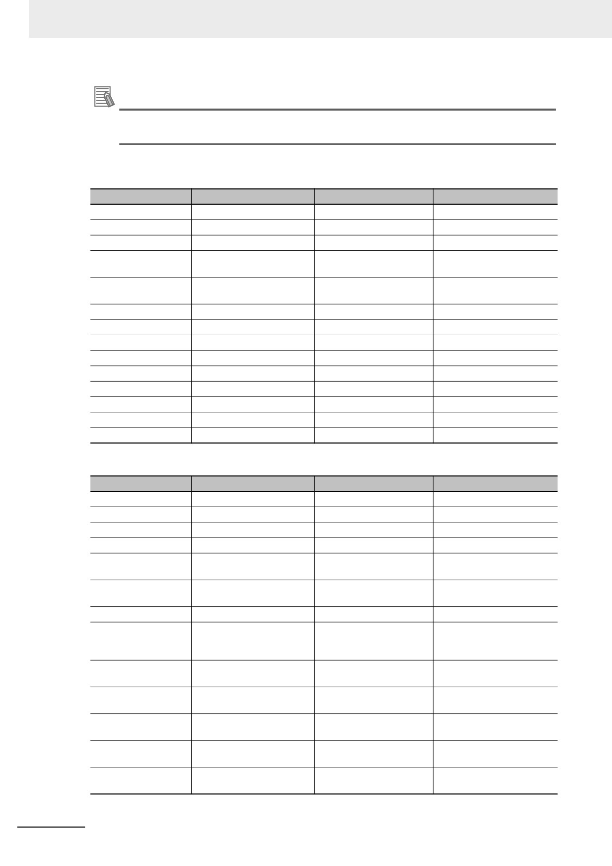
z Omron CJ/CS/NX Series
Device
Bit Address
Word Address
Format
CIO Area
CIO_bit 0000.00-6143.15
------
DDDD.DD
Work Area
W_bit 000.00-511.15
------
DDD.DD
Auxiliary Area
A_bit 000.00-11535.15
------
DDDDD.DD
Holding Area
H_bit 000.00-1535.15
------
DDDD.DD
Timer
T_Flag 0000-4095
------
DDDD
(Completion Flag)
Counter
C_Flag 0000-4095
------
DDDD
(Completion Flag)
Data Memory
D_bit 00000.00-32767.15
------
DDDDD.DD
Extension Data
E0_bit 0.00-32767.15
------
DDDDD.DD
Memory Area
…
(E0-E18)
E18_bit 0.00-32767.15
Extension Data
------
E0 0-32767
DDDDD
Memory(E0-E18)
…
E18 0-32767
CIO Area
------
CIO 0000-6143
DDDD
Work Area
------
W 000-511
DDD
Auxiliary Area
------
A 000-11535
DDDDD
Holding Area
------
H 000-1535
DDDD
Timer Area
------
T 0000-4095
DDDD
Counter Area
------
C 0000-4095
DDDD
Data Memory
------
D 00000-32767
DDDDD
Index memory Area
------
IR 00-15
DD
Data memory Area
------
DR 00-15
DD
A-11
Appendices
Additional Information
As for the NX series, only NX1P2-
is supported. To use the PLC, the settings for the
memory used for CJ-series Units are required. Make the settings on the Controller Unit.
z Omron CP Series
Device
Bit Address
Word Address
Format
Work Area
W_bit 0.00-511.15
------
DDD.DD
Hold Area
H_bit 0.00-1535.15
------
DDDD.DD
Data Area
D_bit 0.00-32767.15
------
DDDDD.DD
Counter
C_Flag 0.00-4095.00
------
DDDD.DD
(Completion Flag)
Timer
T_Flag 0.00-4095.00
------
DDDD.DD
(Completion Flag)
Auxiliary
A_bit 0.00-959.15
------
DDD.DD
CIO Area
CIO_bit 0.00-6143.15
------
DDDD.DD
Work Area
------
W 0-511
DDD
Hold Area
------
H 0-1535
DDDD
Data Area
------
D 0-32767
DDDDD
Counter Area
------
C 0-4095
DDDD
Timer Area
------
T 0-4095
DDDD
Auxiliary Area
------
A 0-959
DDD
CIO Area
------
CIO 0-6143
DDDD
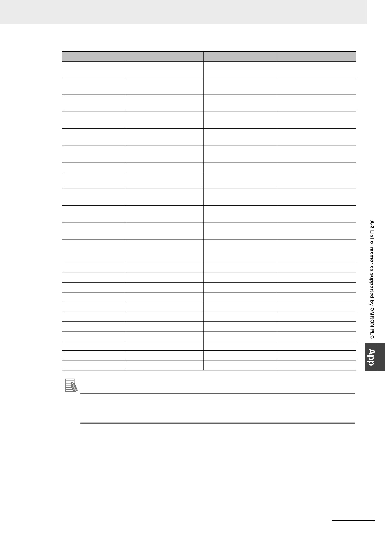
z OMRON CJ/CS/NJ/NX Series Ethernet (UDP Slave)
Device
Bit Address
Word Address
Format
CIO Area
CIO_bit 0000.00-6143.15
------
DDDD.DD
Work Area
W_bit 000.00-511.15
------
DDD.DD
Auxiliary Area
A_bit 000.00-11535.15
------
DDDDD.DD
Holding Area
H_bit 000.00-1535.15
------
DDDD.DD
Timer
T_FLAG 0000-4095
------
DDDD
(Completion Flag)
Counter
C_FLAG 0000-4095
------
DDDD
(Completion Flag)
Data Memory
D_bit 00000.00-32767.15
------
DDDDD.DD
Extension Data
E0_bit 0.00-32767.15
------
DDDDD.DD
Memory Area
…
(E0-E18)
E18_bit 0.00-32767.15
Counter Release
C_RELEASE_STATUS
------
DDDD
Forced Status Area
0000-4095
Timer Release Forced
T_RELEASE_STATUS
------
DDDD
Status Area
0000-4095
Holding Release
H_RELEASE_STATUS
------
DDD.DD
Forced Status Area
0.00-511.15
Work Release Forced
W_RELEASE_STATUS
------
DDD.DD
Status Area
0.00-511.15
CIO Release Forced
CIO_RELEASE_STATUS
------
DDDD.DD
Status Area
0.00-6143.15
A-12
Appendices
Device
Bit Address
Word Address
Format
Holding Set/Reset
H_FORCED_RELEASE
------
DDD.DD
Forced Release Area
0.00-511.15
Holding Forced
H_FORCED 0.00-511.15
------
DDD.DD
Set/Reset Area
Work Set/Reset
W_FORCED_RELEASE
------
DDD.DD
Forced Release Area
0.00-511.15
Work Forced
W_FORCED 0.00-511.15
------
DDD.DD
Set/Reset Area
CIO Set/Reset Forced
CIO_FORCED_RELEASE
------
DDDD.DD
Release Area
0000.00-6143.15
CIO Forced Set/Reset
CIO_FORCED
------
DDDD.DD
Area
0000.00-6143.15
Task Flag Area
TK_FLAG 0-127
------
DDD
Counter Set/Reset
C_FORCED_RELASE
------
DDDD
Forced Release Area
0000-4095
Counter Forced
C_FORCED
------
DDDD
Set/Reset Area
0000-4095
Timer Set/Reset
T_FORCED_RELASE
------
DDDD
Forced Release Area
0000-4095
Timer Forced
T_FORCED
------
DDDD
Set/Reset Area
0000-4095
Extension Data
------
E0 0-32767
DDDDD
Memory
…
(E0-E18)
E18 0-32767
EM Area
------
EM 0-32767
DDDDD
CIO Area
------
CIO 0000-6143
DDDD
Work Area
------
W 000-511
DDD
Auxiliary Area
------
A 000-11535
DDDDD
Holding Area
------
H 000-1535
DDDD
Timer Area
------
T 0000-4095
DDDD
Counter Area
------
C 0000-4095
DDDD
Data Memory
------
D 00000-32767
DDDDD
Index memory Area
------
IR 00-15
DD
Data memory Area
------
DR 00-15
DD
Task Flag Area
------
TK 00-127
DDD
Additional Information
As for the NX series, only NX102-
and NX1P2-
are supported. To use the PLC,
the settings for the memory used for CJ-series Units are required. Make the settings on the Con-
troller Unit.
A-13
Appendices
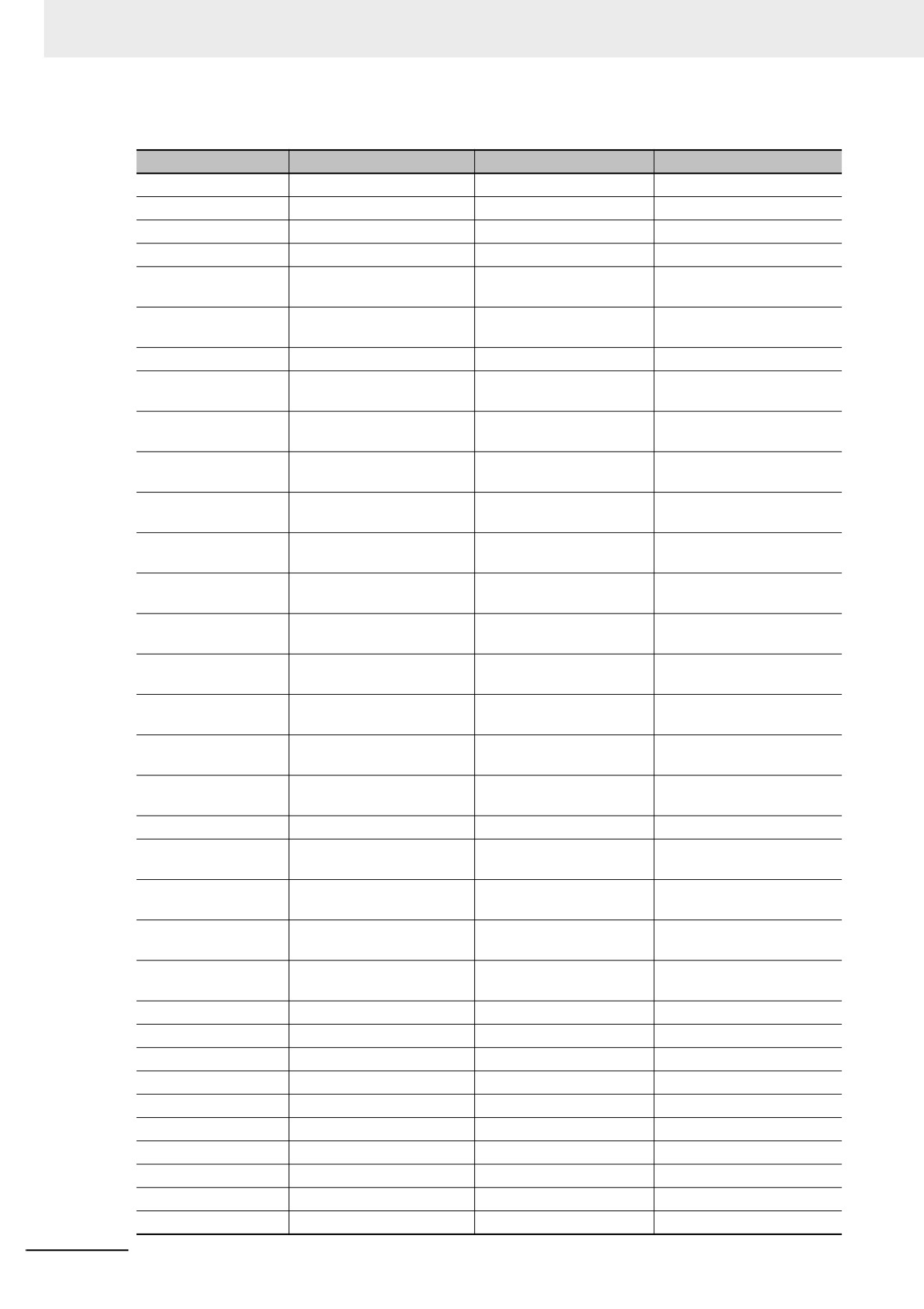
z OMRON CP Series Ethernet (UDP Slave)
Device
Bit Address
Word Address
Format
CIO Area
CIO_bit 0000.00-6143.15
------
DDDD.DD
Work Area
W_bit 000.00-511.15
------
DDD.DD
Auxiliary Area
A_bit 000.00-959.15
------
DDD.DD
Holding Area
H_bit 000.00-1535.15
------
DDDD.DD
Timer
T_FLAG 0000-4095
------
DDDD
(Completion Flag)
Counter
C_FLAG 0000-4095
------
DDDD
(Completion Flag)
Data Memory
D_bit 00000.00-32767.15
------
DDDDD.DD
Counter Release
C_RELEASE_STATUS
------
DDDD
Forced Status Area
0000-4095
Timer Release Forced
T_RELEASE_STATUS
------
DDDD
Status Area
0000-4095
Holding Release
H_RELEASE_STATUS
------
DDD.DD
Forced Status Area
0.00-511.15
Work Release Forced
W_RELEASE_STATUS
------
DDD.DD
Status Area
0.00-511.15
CIO Release Forced
CIO_RELEASE_STATUS
------
DDDD.DD
Status Area
0.00-6143.15
Holding Set/Reset
H_FORCED_RELEASE
------
DDD.DD
Forced Release Area
0.00-511.15
Holding Forced
H_FORCED
------
DDD.DD
Set/Reset Area
0.00-511.15
Work Set/Reset
W_FORCED_RELEASE
------
DDD.DD
Forced Release Area
0.00-511.15
Work Forced
W_FORCED
------
DDD.DD
Set/Reset Area
0.00-511.15
CIO Set/Reset Forced
CIO_FORCED_RELEASE
------
DDDD.DD
Release Area
0000.00-6143.15
CIO Forced Set/Reset
CIO_FORCED
------
DDDD.DD
Area
0000.00-6143.15
Task Flag Area
TK_FLAG 0-31
------
DD
Counter Set/Reset
C_FORCED_RELEASE
------
DDDD
Forced Release Area
0000-4095
Counter Forced
C_FORCED 0000-4095
------
DDDD
Set/Reset Area
Timer Set/Reset
T_FORCED_RELEASE
------
DDDD
Forced Release Area
0000-4095
Timer Forced
T_FORCED
------
DDDD
Set/Reset Area
0000-4095
CIO Area
------
CIO 0000-6143
DDDD
Work Area
------
W 000-511
DDD
Auxiliary Area
------
A 000-959
DDD
Holding Area
------
H 000-1535
DDDD
Timer Area
------
T 0000-4095
DDDD
Counter Area
------
C 0000-4095
DDDD
Data Memory
------
D 00000-32767
DDDDD
Index memory Area
------
IR 00-15
DD
Data memory Area
------
DR 00-15
DD
Task Flag Area
------
TK 00-31
DD
A-14
Appendices
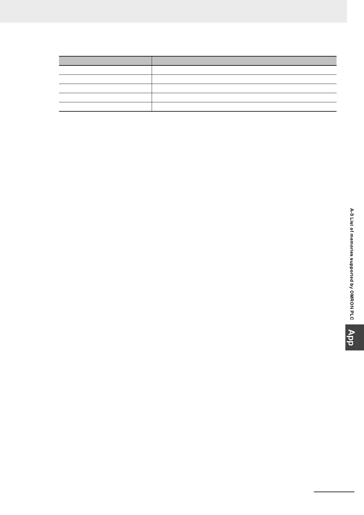
Note
Name
Operation
Forced Reset
Turns OFF (0) the bit/flag and places it in forced status.
Forced Set
Turns ON (1) the bit/flag and places it in forced status.
Forced Set/Reset OFF Release
Turns OFF (0) the bit/flag and releases the forced status.
Forced Set/Reset ON Release
Turns ON (1) the bit/flag and releases the forced status.
Forced Set/Reset Release
Releases the forced status while retaining the ON/OFF status.
A-15
Appendices
A-4
Usage of Forced Address Bit
When the OMRON PLC is connected via Ethernet, there are some special bit addresses:
_FORCED,
_FORCED_RELEASE and
_RELEASE_STATUS.
Usage example:
W_FORCED, W_FORCED_RELEASE and W_RELEASE_STATUS function as follows:
W_FORCED will enforce the address bit to 0 or 1, and then retain it in the forced status.
W_FORCED_RELEASE will enforce the address bit to 0 or 1, but it releases the forced state.
W_RELEASE_STATUS will release the forced status and make no change.
Usage example:
Place two Bit Switch components and one Bit Button component with settings as follows:
Switch No.
Component Name
Address
Switch Type
1
Bit Switch
W_FORCED 0.00
Alternate
2
Bit Switch
W_FORCED_RELEASE 0.00
Alternate
3
Bit Button
W_RELEASE_STATUS 0.00
Set
Perform the test:
Operation 1:
Firstly, touch switch 1 to specify the value to “0 (forced)” and then touch switch 2 to modify the value to
“1” and it causes the bit to be released of the forced state at the same time. Also when the bit is
specified to “1 (forced)” with switch 1, touch switch 2 to modify the bit to “0” and is causes the bit to be
released of the forced state at the same time.
Operation 2:
Firstly, touch switch 1 to specify the value to “0 (forced)” and then touch switch 3, but the bit will be
remained as “0” and it causes the bit to be released of the forced state. Also when the bit is specified to
“1 (forced)”, touch switch 3, but the bit will be remained as “1” and it causes the bit to be released of the
forced state.
Descriptions:
From the above results, it can be concluded that the difference between W_FORCED_RELEASE and
W_RELEASE_STATUS is: the former sets the value of address bit to 0 or 1, and then releases its
forced status, while the latter only releases the forced status of address bit without changing its value.
As W_FORCED_RELEASE is readable and writable, you can allocate it as readable and writable bit.
As W_RELEASE_STATUS is write-only, do not allocate it to reading status processing (e.g. Reading
the ON/OFF status of lamps and switches).
A-16
Revision History
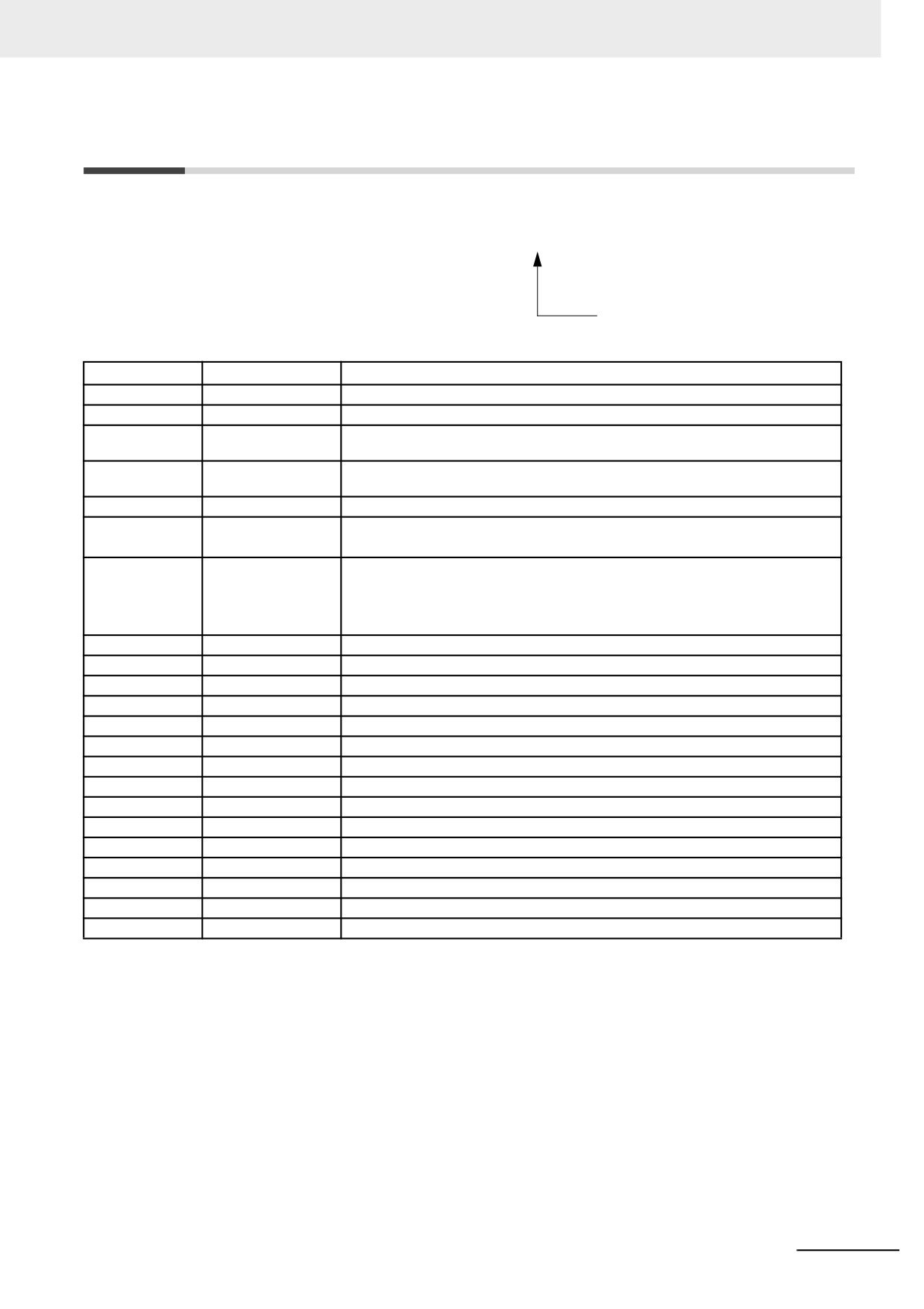
A manual revision code appears as a suffix to the catalog number on the front cover of the manual.
Cat. No. V106-E1-
Revision code
Revision code
Date
Revised content
01
October 2011
Original production
02
February 2012
Changes related to battery.
03
April 2012
Adding descriptions of new functions added into NB5Q/NB7W-TW01B model
and the related contents.
04
August 2012
Adding descriptions and functions of NB3Q-TW00B/TW01B and NB10W-
TW01B models.
05
October 2012
Manual correction and updating.
06
December 2012
• Correction related to the backlight lamp, rubber packing and battery maintenance.
• Adding descriptions of the PictBridge printing function
07
December 2012
• Adding descriptions of the power supply and wire connection in Precautions
for Safe Use.
• Correcting descriptions of the memories related to printing.
• Adding contents to the list of error codes for printing.
08
April 2013
Changes and corrections
09
August 2013
Changes and corrections
10
February 2014
Changes and corrections
11
July 2014
This is a revision accompanied with adding a function to Web Interface.
12
July 2016
Changes and corrections
13
October 2016
Changes and corrections
14
November 2016
Changes related to OS.
15
March 2017
Changes and corrections
16
December 2017
Changes and corrections
17
April 2018
Changes and corrections
18
October 2018
Changes and corrections
19
April 2019
Changed and corrections
20
November 2019
Changes and corrections
21
June 2020
Changes and corrections
22
October 2020
Changes and corrections
Revision-1