Loongson 1C300 Processor User Manual (Version 1.0, 2014) - page 9

The expanded part of USART has added relevant register supporting ISO7816 specification, modified the receiver
and transmitter modules, and added functions of receiving and transmitting error checking and retransmission
control.
19.3 UART0 Split Configuration Introduction
Global fuction interfaces of UART0 in Loongson can be divided into two four-wire serial ports. See section 5.2.4
SHUT_CTRL[31:30] for configuration register.
When UART_split = 0, the pin of UART0 is the global function serial port of UART00.
When UART_split = 1, the UART0 is divided into two controllers: UART00 and UART01. The global functional
pin of UART acts as four-wire serial output of two serial ports: UART00 and UART01, and their relationship is
shown as follows:
Table 19-1 Configuration and function multiplexing of UART split
Original
UART0 functionUart_split= 0
Uart_split= 1
pin-out
UART0_TXD
UART00_TXD
UART00_TXD
UART0_RTS
UART00_RTS
UART00_RTS
UART0_DTR
UART00_DTR
UART01_TXD
UART0_RI
UART00_RI
UART01_RTS
UART0_RXD
UART00_RXD
UART00_RXD
UART0_CTS
UART00_CTS
UART00_CTS
UART0_DSR
UART00_DSR
UART01_RXD
UART0_DCD
UART00_DCD
UART01_CTS
The function register of UART0 and UART01 is completely the same with the register described in 19.4, but the
access base address is different. Therein, the base address of register physical address of UART00 is 0xbfe4_0000,
and that of UART01 is 0xbfe4_1000.
19.4 Register Description
Loongson 1C has 12 UART/USART (marked as URT) interface, and its function is completely the same with
functional register, but the access base address is different.
Ɣ The base address of register physical address of URT0 is 0xbfe4_0000.
ƔThe base address of register physical address of URT1 is 0xbfe4_4000.
Ɣ The base address of register physical address of URT2 is 0xbfe4_8000.
Ɣ The base address of register physical address of URT3 is 0xbfe4_c000.
Ɣ The base address of register physical address of URT4 is 0xbfe4_c400.
Ɣ The base address of register physical address of URT5 is 0xbfe4_c500.
Ɣ The base address of register physical address of URT6 is 0xbfe4_c600.
Ɣ The base address of register physical address of URT7 is 0xbfe4_c700.
Ɣ The base address of register physical address of URT8 is 0xbfe4_c800.
Ɣ The base address of register physical address of URT9 is 0xbfe4_c900.
Ɣ The base address of register physical address of URT10 is 0xbfe4_ca00.
Ɣ The base address of register physical address of URT11 is 0xbfe4_cb00.
19.4.1 Data register (DAT)
English name: Data transmission register
-158-
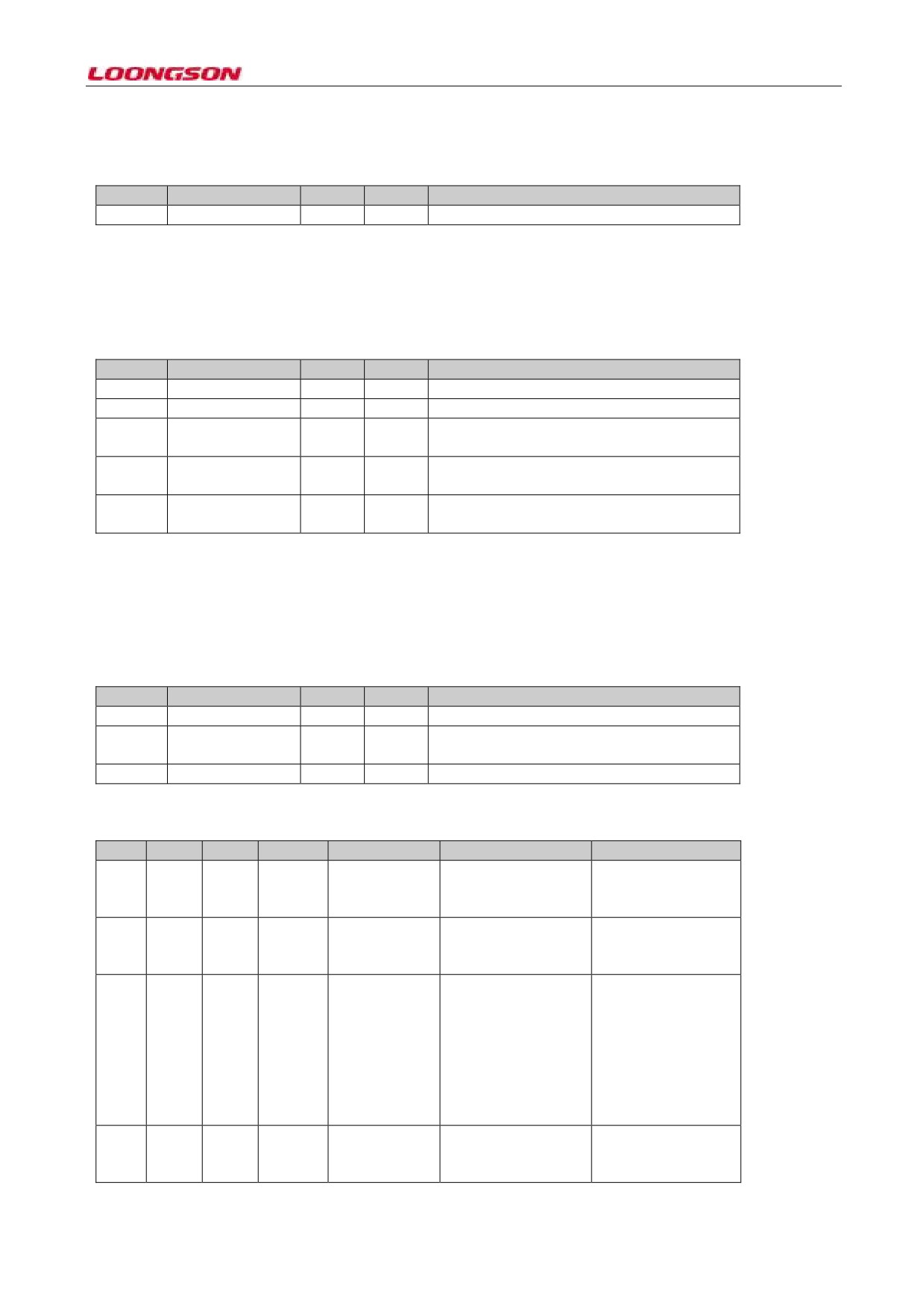
Register bit width: [7:0]
Offset: 0x00
Reset value: 0x00
Bit field
Bit field name
Bit width
Access
Description
7:0
Tx FIFO
8
W
Data transmitter register
19.4.2 Interrupt enable register (IER)
English name: Interrupt enable register
Register bit width: [7:0]
Offset: 0x01
Reset value: 0x00
Bit field
Bit field name
Bit width
Access
Description
7:4
Reserved
4
RW
Reserved
3
IME
1
RW
Modem status interrupt enables '0' - off '1' -on
2
ILE
1
RW
Receiver line status interrupt enable '0' - off '1'
-on
1
ITxE
1
RW
Transfer and storage register is empty interrupt
enable '0' - off '1' -on
0
IRxE
1
RW
Receive valid data interrupt enable '0' - off '1'
-on
19.4.3 Interrupt identification register (IIR)
English name: Interrupt source register
Register bit width: [7:0]
Offset: 0x02
Reset Value: 0xc1
Bit field
Bit field name
Bit width
Access
Description
7:4
Reserved
4
R
Reserved
3:1
II
3
R
Interrupt source indicating bit, details in the
table below
0
INTp
1
R
Interrupt indicating bit
Interrupt control function table:
Bit 3
Bit 2
Bit 1
Priorities
Interrupt type
Interrupt source
Interrupt reset control
0
1
1
1st
Receive
lineOdd-even, overflow orReading LSR
status
framing error, or break
interrupt
0
1
0
2nd
Receive validThe character numberThe character number
number
of FIFO reaches theof FIFO is lower than
trigger level.
trigger value.
1
1
0
2nd
Receive timeout
There is at least oneReading
reception
character in FIFO, butFIFO
there is
no any
operation within the
time
of
four
characters, including
read
and
write
operations.
0
0
1
3rd
Transmit, saveEmpty transmissionWrite data to THR or
and storage
save register
multiple IIR
Empty device
-159-

0
0
0
4th
Modem status
CTS, DSR, RI orRead MSR
DCD.
19.4.4 FIFO control register (FCR)
English name: FIFO control register
Register bit width: [7:0]
Offset: 0x02
Reset value: 0xc0
Bit field
Bit field name
Bit width
Access
Description
7:6
TL
2
W
Receive the trigger value '00' -1 byte '01' -4
bytes '10' -8 bytes '11' -14 bytes from interrupt
request of FIFO
5:3
Reserved
3
W
Reserved
2
Txset
1
W
'1' clears the content sent to FIFO, and reset its
logic
1
Rxset
1
W
'1' clears the content received from FIFO, and
reset its logic
0
Reserved
1
W
Reserved
19.4.5 Line control register (LCR)
English name: Line control register
Register bit width: [7:0]
Offset: 0x03
Reset value: 0x03
Bit field
Bit field name
Bit width
Access
Description
7
dlab
1
RW
Fractional frequency latch access bit
'1 '- Access operation fractional frequency latch
'0 '- Access operation normal register
6
bcb
1
RW
Interrupt control bit
'1' -the serial output is set to 0 (interrupt status)
'0'—normal operation
5
spb
1
RW
Specified parity check bit
'0 '- No specified parity check bit
'1'
-if LCR[4] bit is 1, transfer and check the
parity check bit is 0. If LCR[4] bit is 0, transfer
and check the parity check bit is 1.
4
eps
1
RW
Parity check bit selection
'0'
-there is an odd number of
1 in each
character (including data and parity check bit)
1 '- there are an even number of characters in
each character
3
pe
1
RW
Parity check bit enable
'0 '- No parity check bit
'1'
- generate the parity check bits in output,
and judge the parity check bits in input.
2
sb
1
RW
Digits of defined generation stop bit
'0 '- 1 stop bit
‘1’ -in case of five-bit length, there is 1.5 stop
bits, and other lengths are 2 stop bits.
1:0
bec
2
RW
Set the digits of each character
'00' -5 bit '01' -6 bit
'10' -7 bit '11' -8 bit
-160-
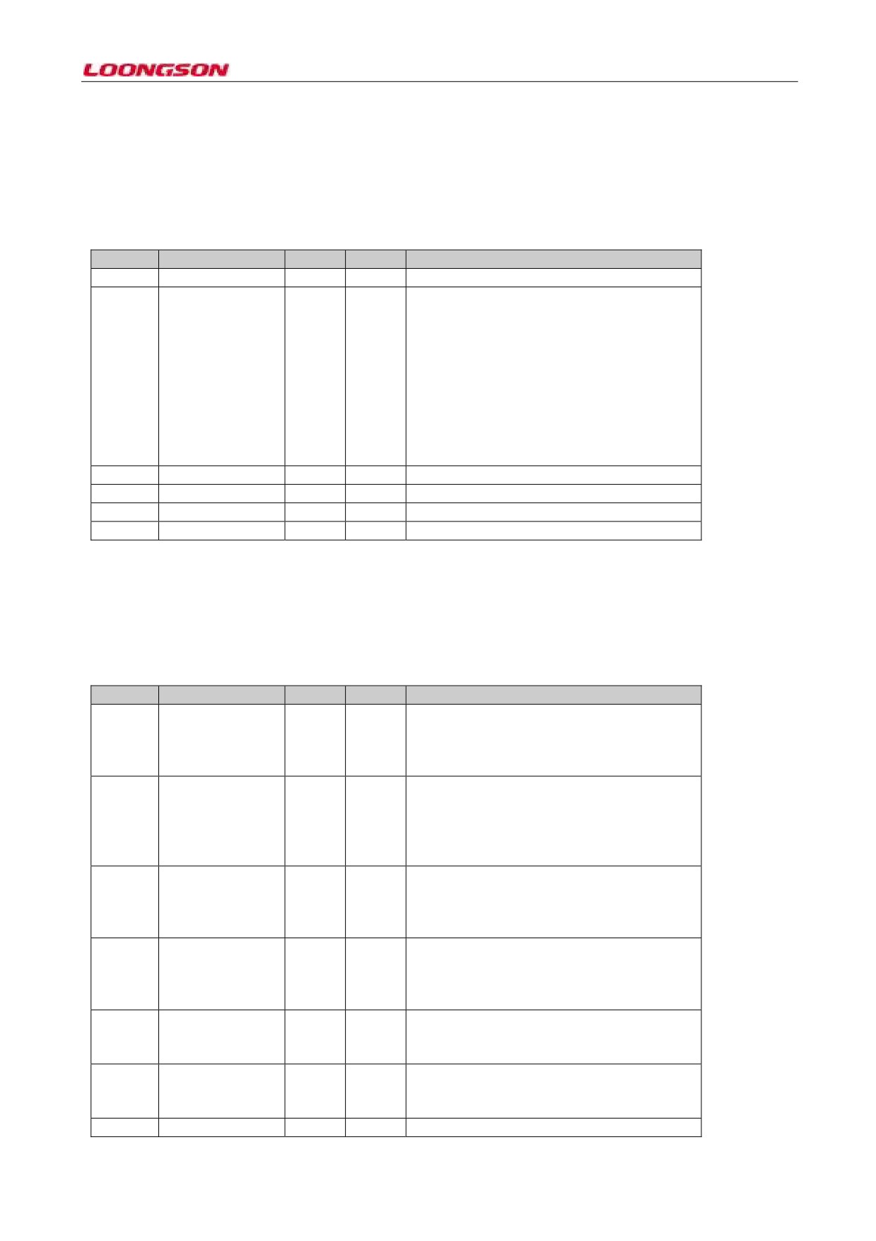
19.4.6 MODEM control register (MCR)
English name: Modem control register
Register bit width: [7:0]
Offset: 0x04
Reset value: 0x00
Bit field
Bit field name
Bit width
Access
Description
7:5
Reserved
3
W
Reserved
4
Loop
1
W
Loopback mode control bit
'0'—normal operation
'1'—- loopback mode. In loopback mode, TXD
output has been 1, and the output shift register
is directly connected to input shift register.
Other connections are as follows.
DTR DSR
RTS CTS
Out1 RI
Out2 DCD
3
OUT2
1
W
Connect to DCD input in the loopback mode
2
OUT1
1
W
Connect to RI input in the loopback mode
1
RTSC
1
W
RTS signal control bit
0
DTRC
1
W
DTR signal control bit
19.4.7 Line status register (LSR)
English name: Line status register
Register bit width: [7:0]
Offset: 0x05
Reset value: 0x00
Bit field
Bit field name
Bit width
Access
Description
7
ERROR
1
R
Error indicating bit
'1' - at least one of parity check bit error, frame
error or interrupt.
'0 '- No error
6
TE
1
R
Empty transmission indicating bit
'1' -transfer FIFO and transfer shift register are
empty. Cleared when writing data to the FIFO
transmission
'0 '- with data
5
TFE
1
R
Transmit empty FIFO bit indicating bit
'1'
-the current transfer FIFO is empty, reset
when writing data to transfer FIFO
'0 '- with data
4
BI
1
R
Break interrupt indicating bit
1' -receive start bit + data + parity bit + stop
bit are all 0, namely, there is interrupt
'0 '- no interrupt
3
FE
1
R
Frame error indicating bit
'1 '- No stop bit in the received data
'0 '- No error
2
PE
1
R
Error bit of parity check bit
'1 '- parity error in current receiving data
'0 '- No parity error
1
OE:
1
R
Data overflow indicating bit
-161-
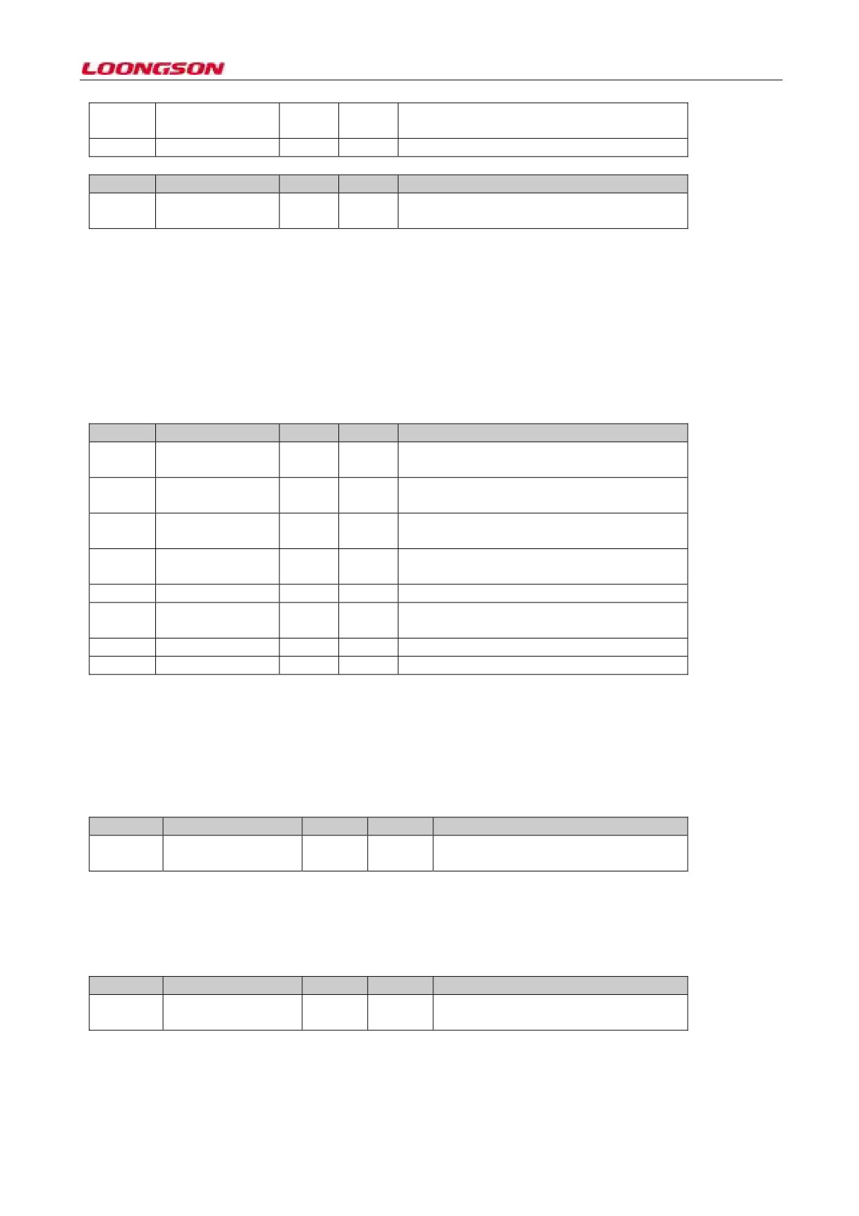
'1 '- Data overflow
'0 '- No overflow
0
DR
1
R
Indicating bit of valid received data
Bit field
Bit field name
Bit width
Access
Description
'0 '- No data in the FIFO
'1 '- with data in the FIFO
During the read operation of the register, LSR[4:1] and LSR[7] are cleared; when writing data to transfer FIFO,
LSR[6:5] is cleared, and LSR[0] judges received FIFO.
19.4.8 MODEM status register (MSR)
English name: Modem status register
Register bit width: [7:0]
Offset: 0x06
Reset value: 0x00
Bit field
Bit field name
Bit width
Access
Description
7
CDCD
1
R
The opposite of DCD input value or connect
Out2 in loopback mode
6
CRI
1
R
The opposite of RI input value or connect to
Out1 in loopback mode
5
CDSR
1
R
The opposite of DSR input value or connect to
DTR in loopback mode
4
CCTS
1
R
The opposite of CTS input value or connect to
RTS in loopback mode
3
DDCD
1
R
DDCD indicating bit
2
TERI
1
R
RI edge detection. RI status changes from low
to high
1
DDSR
1
R
DDSR Indication bit
0
DCTS
1
R
DCTS Indication bit
19.4.9 Fractional frequency latch
English name: Fractional frequency latch 1
Register bit width: [7:0]
Offset: 0x00
Reset value: 0x00
Bit field
Bit field name
Bit width
Access
Description
7:0
LSB
8
RW
Fractional frequency latch storage low 8
bit
English name: Fractional frequency latch 2
Register bit width: [7:0]
Offset: 0x01
Reset value: 0x00
Bit field
Bit field name
Bit width
Access
Description
7:0
MSB
8
RW
Fractional frequency latch storage high 8
bit
19.5 USART Register Description
On the basis of UART, USART adds registers CR, MR and FIDIR supporting ISO7816 specification.
-162-
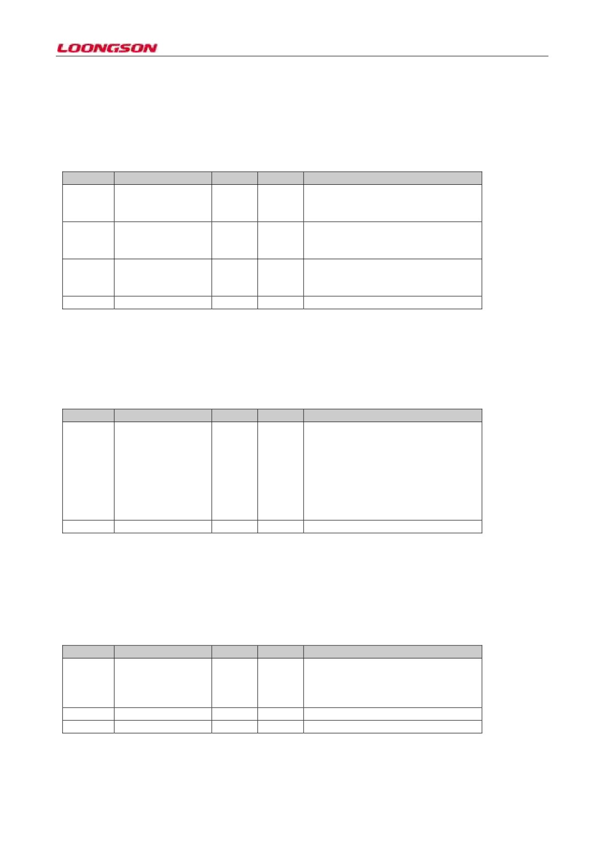
19.5.1 Control register (CR)
English name: control register
Register bit width: [7:0]
Offset: 0x8
Reset value: 0x00
Bit field
Bit field name
Bit width
Access
Description
0
UART_EN
1
RW
Serial port enable
0: Disable
1: Enable
1
IRDA_EN
1
RW
Infrared interface enable
0: Disable
1: Enable
2
SC_EN
1
RW
Smart card interface enable
0: Disable
1: Enable
3-7
-
-
-
Reserved
19.5.2 Mode register (MR)
English name: Mode register
Register bit width: [7:0]
Offset: 0x9
Reset value: 0x00
Bit field
Bit field name
Bit width
Access
Description
0-3
USART_MODE
4
RW
USART working mode:
0000: Normal
0001: Serial
0010: Hardware handshake
0011: modem
0100: ISO7816 T=0
0110: ISO7816 T=1
1000: IrDA Others: reserved
4-7
-
-
-
Reserved
19.5.3 FI/DI parameter register (FIDIR)
English name: Mode register
Register bit width: [31:0]
Offset: 0xA
Reset value: 0x00000000
Bit field
Bit field name
Bit width
Access
Description
0-10
FI_DI_RATIO
11
RW
0: ISO7816 mode doesn’t generate Baud
rate signal
1~2047: ISO7816 produces Baud rate
signal
11-31
-
-
-
Reserved
-163-
20 NAND Controller
20.1 NAND Controller Structural Description
NAND FLASH controller supports four chip selections and four RDY signals at most, and the controller supports
the operation of two types of FLASH (SLC and MLC), supports 512Bytes, 2K, 4K, 8K page size FLASH
operations, supports single chip of 8GB, 32GB for four chips. NAND FLASH controller supports the system
startup, and the startup mode includes ECC mode startup and ordinary mode startup.
The system startup mode selection includes two types, as is shown in following table:
Startup mode
Configuration
Note
ECC mode
NAND_CLE external pull-up
The content of the first page in external NAND FLASH
Start
must be data produced by original data via RS (204,188)
decoding.
Normal
NAND_CLE
external
The first page data of the external NAND FLASH is
startup
pull-down
ordinary original data.
20.2 NAND Control Register Configuration Description
The list of NAND internal registers is as follows:
Address
Register name
0xbfe7_8000
NAND_CMD
0xbfe7_8004
ADDR_C
0xbfe7_8008
ADDR_R
0xbfe7_800C
NAND_TIMING
0xbfe7_8010
ID_L
0xbfe7_8014
STATUS
0xbfe7_8018
NAND_PARAMETER
0xbfe7_801C
NAND_OP_NUM
0xbfe7_8020
CS_RDY_MAP
0xbfe7_8040
DMA
20.2.1 Command register (NAND_CMD)
Bit
Bit field name
RW
Description
(read/w
rite)
31
DMA_REQ
R/-
In non-ECC mode, NAND sends DMA request.
30
ECC_DMA_REQ
R/-
In ECC mode, NAND sends DMA request.
29:25
STATUS
R/-
Internal status machine (for testing)
24
R/-
Reserved
23: 20
NAND_CE
R/-
Selection of external NAND chips and four
bits
correspond to four chip selections respectively.
0
stands for being chosen.
19: 16
NAND_RDY
R/-
In case of RDY of external NAND chip, the
corresponding relationship is consistent with
NAND_CE, and 1 indicates ready.
15
Reserved
14
Wait_rs_rd_done
R/W
1 indicates waiting for ECC read to finish (used in
ECC read)
13
INT_EN
R/W
NAND interrupt enable signal, and
1 indicates
-164-
enable interrupt.
12
RS_WR
R/W
1 indicates that ECC function is started in read
operation.
11
RS_RD
R/W
1 indicates that ECC function is started in read
operation.
10
done
R/W
1 indicates that the operation is finished, and it needs
the software to clear.
9
Spare
R/W
1 indicates the operation occurs in SPARE area of
NAND.
8
Main
R/W
1 indicates the operation occurs in MAIN area of
NAND.
7
Read status
R/W
1 indicates the status operation of read NAND.
6
Reset
R/W
1 indicating Nand reset operation
5
read id
R/W
1 indicating reading ID operations
4
blocks erase
R/W
Erase the flag continuously, and default 0; 1 is valid,
and the number of continuous erasing blocks are
decided by nand_op_num.
3
erase operation
R/W
1 indicating erasure operation
2
write operation
R/W
1 indicating write operation
1
read operation
R/W
1 indicating read operation
0
command valid
R/W
1 indicates the command is valid, and the hardware
is automatically cleared after operation.
20.2.2 Page offset address register (ADDR_C)
Bit
Bit field name
RW (read/write)
Description
31:14
R/-
Reserved
13:0
R/W
Read, write and erase the initial address of the
Nand_Col
page address operation
(it must be aligned by words, multiples of 4),
and its corresponding relation with page size is:
512Bytes: it only needs to fill out [8:0]
2K: it needs to fill out
[11:0], and
[12]
represents spare area, and [11:0] represents page
offset address.
4K: it needs to fill out
[12:0], and
[12]
represents spare area, and [11:0] represents page
offset address.
8K: it needs to fill out
[13:0], and
[12]
represents spare area, and [11:0] represents page
offset address.
20.2.3 Page address register (ADDR_R)
Bit
Bit field name
RW (read/write)
Description
31:25
R/-
Reserved
24:0
Nand_Row
R/W
Read, write and erase operations start address, page
address, and the address consists of:
{Chip selection, pages}
The chip selection is fixed to 2 bits, and the page
number is determined based on actual capacity of
single particle. For example, 1M page is [19:0], and
[21:20] is used select which chip among 4 chips.
-165-
20.2.4 Timing sequence register (NAND_TIMING)
Bit
Bit field name
RW
Description
(read/write)
31:16
R/-
Reserved
15:8
Hold cycle
R/W
The cycle number required by NAND command
significant, default 4
7:0
Wait cycle
R/W
Total clock cycle number required by NAND
one-time read and write, default 18, and configure
to 8’hb in ECC mode
20.2.5 ID register (ID_L)
Bit
Bit field name
RW
Description
(read/write)
[31:0]
ID (310)
R/-
ID (310)
20.2.6 ID and status register (STATUS & ID_H)
Bit
Bit field name
Access
31:24
R/-
Reserved
23:16
STATUS
R/-
Current reading and writing completion status of
NAND device
15:0
ID (4732)
R/-
ID high 16 bits (if the ID has only
5 bytes,
ID[47:40] is 0)
20.2.7 Parameter configuration register (NAND_PARAMETER)
Bit
Bit field name
RW
Description
(read/write)
31:30
R/-
Reserved
29:16
op_scope
R/W
Each capable operating range, the configuration
is as follows:
1. Operate main area, and configure it to the size
of the main area in a page
2. Operate spare area, and configure it to the size
of the spare area in a page
3. Operate the main and spare areas, and
configure to the size of the main and spare areas
in a page
15
R/-
Reserved
14:12
ID_number
R/W
The number of bytes of the ID
11:8
External
grain
R/W
0:1 Gb (2K page)
capacity size
1:2 Gb (2K page)
2:4 Gb (2K page)
3:8 Gb (2K page)
4:16 Gb (4K page)
5:32 Gb (8K page)
6:64 Gb (8K page)
7:128 Gb (8K page)
9:64 Mb (512B page)
a: 128Mb (512B page)
b: 256Mb (512B page)
c: 512Mb (512B page)
-166-
d: 1Gb (512B page)
7:0
R/-
Reserved
20.2.8 Operating number register (NAND_OP_NUM)
Bit
Bit field name
RW
Description
(read/write)
31:0
NAND_OP_NUM
R/W
NAND read and write Byte numbers (must be
aligned by words, and multiples of
4); erase
block number
20.2.9 Map register (CS_RDY_MAP)
Four CSs of NAND are automatically generated by the accessed address hardware, and CS0/RDY0 corresponds to
the lowest space, CS1/RDY1 to the next lowest space, and so forth. If it’s necessary to adjust the relationship
between external chip and NAND address, remap cs_rdy 1/2/3 by setting this register.
Bit
Bit field name
RW
Description
(read/write)
31:28
rdy3_sel
R/W
rdy3 signal is mapped from chip pin to NAND
controller
4’b0001:NAND_RDY[0]
4’b0010:NAND_RDY[1]
4’b0100:NAND_RDY[2]
4’b1000:NAND_RDY[3]
27:24
cs3_sel
R/W
rdy3 signal is mapped from NAND controller to
chip pin
4’b0001:NAND_CS[0] 4’b0010:NAND_CS[1]
4’b0100:NAND_CS[2] 4’b1000:NAND_CS[3]
23:20
rdy2_sel
R/W
rdy2 signal is mapped from chip pin to NAND
controller
4’b0001:NAND_RDY[0]
4’b0010:NAND_RDY[1]
4’b0100:NAND_RDY[2]
4’b1000:NAND_RDY[3]
19:16
cs2_sel
R/W
cs2 signal is mapped from NAND controller to chip
pin
4’b0001:NAND_CS[0] 4’b0010:NAND_CS[1]
4’b0100:NAND_CS[2] 4’b1000:NAND_CS[3]
15:12
rdy1_sel
R/W
rdy1 signal is mapped from chip pin to NAND
controller
4’b0001:NAND_RDY[0]
4’b0010:NAND_RDY[1]
4’b0100:NAND_RDY[2]
4’b1000:NAND_RDY[3]
11:8
cs1_sel
R/W
cs1 signal is mapped from NAND controller to chip
pin
4’b0001:NAND_CS[0] 4’b0010:NAND_CS[1]
4’b0100:NAND_CS[2] 4’b1000:NAND_CS[3]
7:0
R/-
Reserved
20.2.10 DMA read and write data register (DMA_ADDRESS)
Bit
Bit field name
RW
Description
(read/write
-167-
)
[31£º0]
DMA_ADDRESS
R/W
For the access address where DMA reads and writes
NAND flash data
(except ID/STATUS), the
read/write address is the same and the read/write
direction is implemented by DMA configuration.
20.3 NAND ADDR Description
Taking 2K-page NAND flash for example, it’s defined as follows:
The size of the main area in each page is 2KB, and that of the spare area is 64B
main_op = NAND_CMD[8];
spare_op = NAND_CMD[9];
addr_in_page
={A11, A10.. A2, A1, A0}=ADDR_C page_number
={
…A30,A29,A28,A27…A13,A12}=
ADDR_R
Total capacity of computational formula of main area NAND flash
Capacity=2^(ADDR_C-1) * 2^(ADDR_R)*8bit = 2K*2^(ADDR_R)*8bit
NAND address space is exampled in the following table:
Table 20-1 NAND address space diagram
I/O
0
1
2
3
4
5
6
7
Column1
1st Cycle
A0
A1
A2
A3
A4
A5
A6
A7
Column2
2nd Cycle
A8
A9
A10
A11
L.
L.
L.
L.
Row1
3rd Cycle
A12
A13
A14
A15
A16
A17
A18
A19
Row2
4th Cycle
A20
A21
A22
A23
A24
A25
A26
A27
Row3 (Note)
5th Cycle
A28
A29
A30
A31
A32
A33
….
….
(Notes: the maximum Row corresponding to 2K-page 1Gb NAND flash is A27, and only Column1~2 and
Row1~2 are used instead of Row3 to the address to NAND flash. In the configuration of NAND parameters,
attention should be paid to the model configuration, or data won’t be read and the controller may die, etc.)
For NAND particles in system board, if only the spare area is operated, A11=1 will be the only sign. Thus, when
the software configures the internal register, it’s necessary to configure A11 and spare_op to 1 (see Examples5).
See Examples2 for wrong examples.
For NAND particles in system panel, if only the spare area is operated, A11=1 is the only sign. Thus, when the
software configures the internal register, it’s necessary to configure A11 and spare_op to 0 (see Examples1). See
Examples4 for wrong examples.
For NAND particles in system panel, if only main+spare areas are operated, A11 may be 0 (see Examples3), and
may also be 1 (See Examples6)
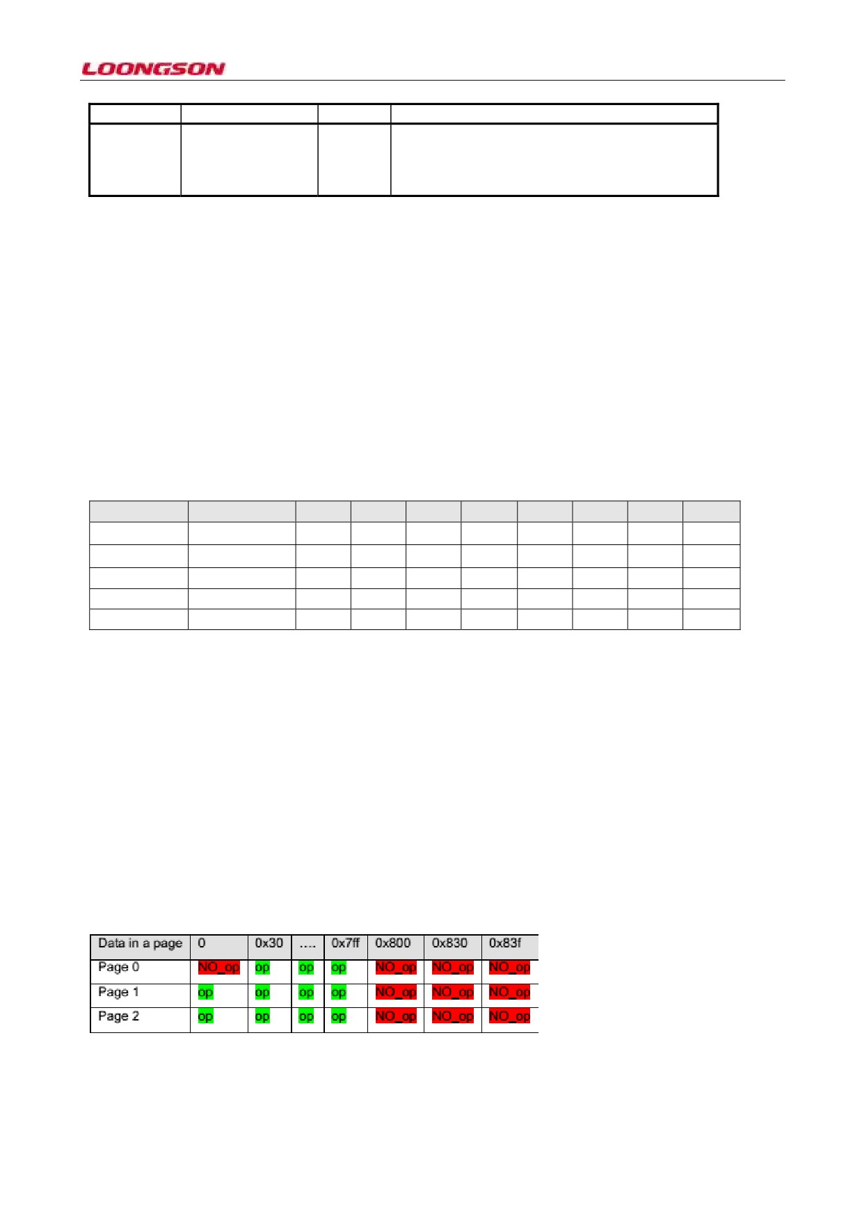
Examples1: (In non-ECC mode, One-page data in NAND particles is only located in 0x0-0x83f. The first op
indicates the initial read and write data, and the following ops indicate the subsequent read and write data; NO_op
indicates the data that can’t be read and written by this NAND configuration.
(spare_op = 1’b0 & main_op =1’b0) equal to (spare_op = 1’b0 & main_op=1’b1); ADDR_C =0x30
Examples2:
spare_op=1’b1 & main_op=1’b0; ADDR_C = 0x30 (Wrong configuration!! The initial operation isn’t performed in
spare area, and the figure below shows the possible sequence of wrong access)
-168-
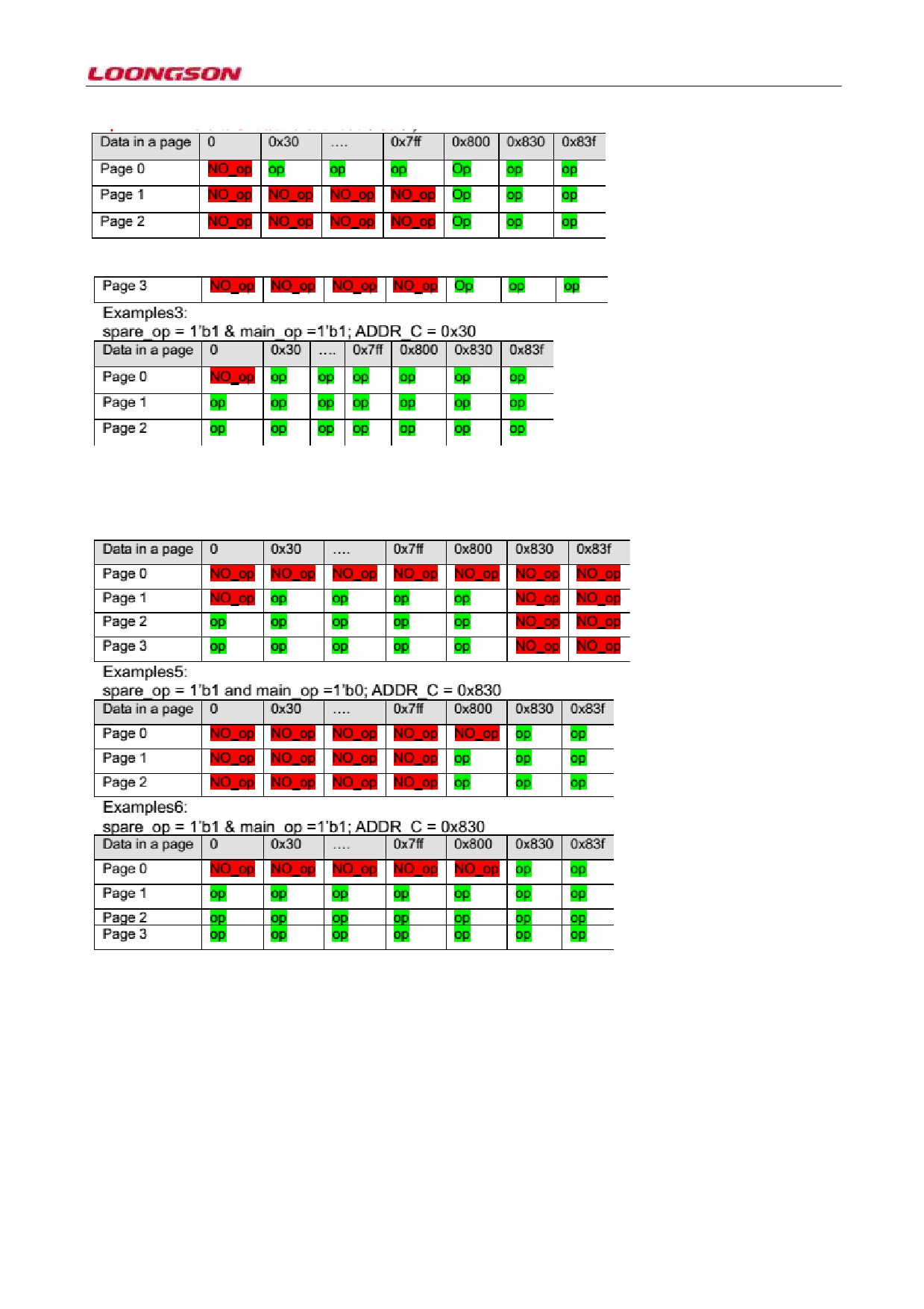
Examples4:
(spare_op=1’b0 & main_op=1’b0),
(equal to spare_op=1’b0 & main_op=1’b1); ADDR_C=0x830: Wrong
configuration!! The initial operation is performed in spare area, and the figure below shows the possible sequence of
wrong access)
The configuration of 512B-page and 2KB-page NAND flash is similar, but there are some differences that need
attention:
The size of the main area in each page is 512B, and that of the spare area is 16B Therein, the main area is divided
into two 256B areas, each of which is addressed by A0~A7. In read and write operations, commands 0x00, 0x01
and 0x50 are sent to choose which 256B area or spare area (Don’t care about the software; the hardware selects
automatically, for example, when the configuration NAND controller writes
0x100, the hardware will
automatically send it to high 256B area).
Transmit address command sequence is as follows:
-169-
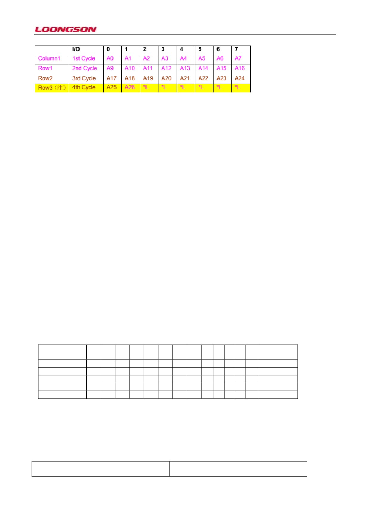
(Notes: when the capacity of Nand flash is 64Mb, 128Mb and 256Mb, their corresponding largest column
addresses of ADDR_R are A22, A23 and A24 respectively. Only address commands of Column1 and Row1~2 are
sent three times, and Row3 won’t be sent; when the capacity is 512Mb and 1Gb, Row3 needs to be sent.
4K/8K page- and 2K page-configurations are the same. The 4K page configuration has 4KB main area and 128B
spare area; the 8K page configuration has 8KB main area and 640B spare area. Need to transmit five address
commands.
20.4 Examples of Nand-flash Read and Write Operations
The “command valid” bit of the register can’t be set simultaneously with other read and write enable bits. Only
after the operation is set, can ‘command valid’ bit is set.
For example, to read the data of Main area, the operation is divided into two steps:
a. firstly, NAND_CMD = 0x102
b. Then, NAND_CMD = 0x103
20.5 NAND ECC Description
The hardware integrates ECC function, and ECC adopts the RS (204,188) method to encode and decode. But in
software configuration, attention should be paid to the following:
1. In reading and writing NAND, 0 is recommended for the internal address (ADDR_C) of Page;
2. In each PAGE, NAND has 2048Bytes. After coding and decoding by RS (204,188), only the first 2040Bytes
will be used, and 8 bytes will not; after the adoption of ECC, the NAND utilization rate is 188/204;
3. In operand configuration, in operating one page, the op_num in NAND is configured to multiples of 204 (in the
unit of byte); in DMA configuration, the operand is the multiples of 47(188/4) (in the unit of word).
4. ECC operation and OOB operation may be separated. For example, after one page finishes ECC read/write, its
OOB can be operated.
After the completion of ECC operation, all contents can be read back by common way, including original data and
the data added by ECC check (the configuration operand op_num and DMA are the same). Check ability: 8 bytes
may be corrected at most, and 1-8 bits may go wrong among those Bytes.
64bits are wrong in the first line of data, just equal to 8 bytes, which can be corrected; although 9bits are wrong in
the last of data, and scatter among 9Bytes, which can’t be corrected.
Original data
ff
ff
ff
ff
ff
ff
ff
ff
ff
ff
ff
ff
(204Bytes)
Data 1
00
00
00
00
00
00
00
00
ff
ff
ff
ff
…
Correctable
Data 2
1
ff
ff
ff
ff
ff
ff
ff
ff
ff
ff
ff
…
Correctable
Data 3
fe
ff
ff
ff
ff
ff
ff
ff
ff
ff
ff
ff
…
Correctable
Data 4
1
2
3
4
5
6
07
08
ff
ff
ff
ff
…
Correctable
Data 5
fe
fe
fe
fe
fe
fe
fe
fe
fe
ff
ff
ff
…
Uncorrectable
20.6 NAND BOOT Description
The NAND BOOT supports the NAND flash boot in 512B, 2K page, 4K page and 8K page. Based on the capacity
and pagesize of FLASH, the pull-up and pull-down resistors of NAND_D[7:6] are configured (they must
correspond to each other, or it may die, etc.). This is shown in figure below:
In NAND boot, configure the particle capacity of
NAND_D [7:6] nand _type
NAND flash
-170-
11 indicates the capacity is equal to 2GB (2K
page/4K page/8K page)
10 indicates the capacity is 1GB (2K page)
01 indicates the capacity is 512MB (512 Bytes
page)
00: it indicates the capacity is low and equal to
256MB (512 Bytes page)
In NAND boot, 1K bytes will be fetched from Page 0 for the chip initialization. If it’s 512B, two pages will be
read; if it’s 2K page or larger, 1K bytes will be read. The system initial code needs to start from 0 byte from Page
0.
Through the pulling up and down of NAND_CLE, NAND BOOT may choose ECC boot or non-ECC boot. Their
differences are: ECC adopts RS(204,188) code, and in ECC boot 1020 bytes are read, 940 bytes of which are valid
data, and the rest coded data. (Notes: in ECC boot, 512B page isn’t supported.)
-171-
21 RTC
21.1 Overview
Loongson 1C real-time clock unit can be configured after the main board is powered on, and after the main board
is powered off, the unit still runs normally relying on the battery in main board. RTC unit only consumes several
microwatts during operation.
RTC is driven by the external 32.768KHZ crystal oscillator, and after the frequency division by configurable
frequency divider, this clock is used to count, and update hour, minute, second, day, month, and year. At the
meantime, the clock is also used to generate various timing and counting interrupts.
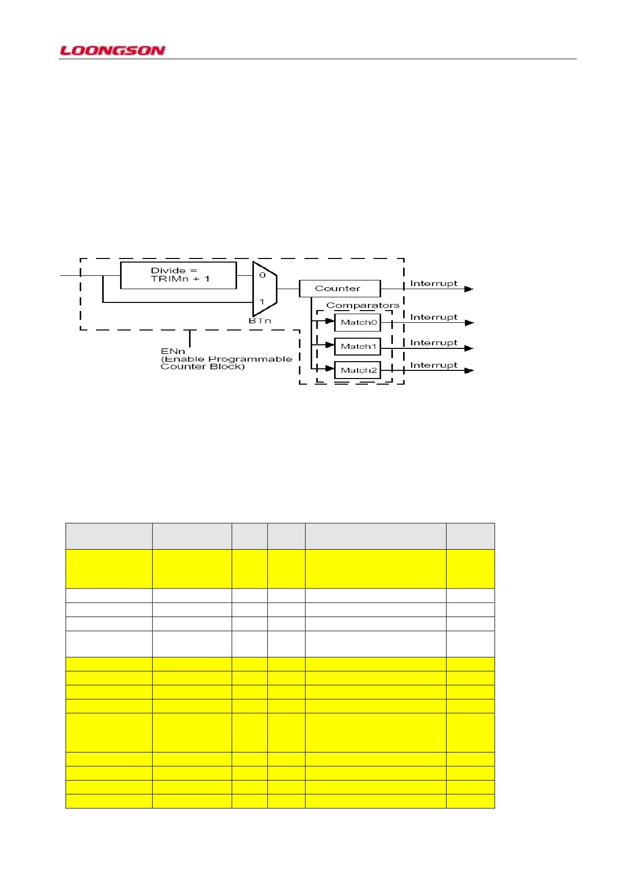
RTC unit consists of counter and timer, and its architecture is shown in the figure below:
Figure 21-1 RTC block architecture diagram
21.2 Register Description
RTC module register is located in 0xbfe6_4000
In 16KB address space of -0xbfe6_7fff, its base address is 0xbfe6_4000, and the bit width of all registers is 32-bit.
21.2.1 Register address list
Name
Address
Bit
RW
Description
Reset
width
value
sys_toytrim
32
For the frequency division
0xbfe6_4020
W
factor of 32.768kHz
(Counter clock)
sys_toywrite0
0xbfe6_4024
32
W
TOY low 32-bit value read-in
sys_toywrite1
0xbfe6_4028
32
W
TOY high 32-bit value read-in
sys_toyread0
0xbfe6_402C
32
R
TOY low 32-bit value read-out
sys_toyread1
0xbfe6_4030
32
R
TOY high
32-bit
value
read-out
sys_toymatch0
0xbfe6_4034
32
RW
TOY timer interrupt 0
sys_toymatch1
0xbfe6_4038
32
RW
TOY timer interrupt 1
sys_toymatch2
0xbfe6_403C
32
RW
TOY timer interrupt 2
sys_rtcctrl
0xbfe6_4040
32
RW
TOY and RTC control register
sys_rtctrim
32
RW
For the frequency division
0xbfe6_4060
factor of 32.768kHz
(Timer clock)
sys_rtcwrite0
0xbfe6_4064
32
RW
RTC timer count write-in
sys_rtcread0
0xbfe6_4068
32
RW
RTC timer counter read-out
sys_rtcmatch0
0xbfe6_406C
32
RW
RTC clock timer interrupt 0
sys_rtcmatch1
0xbfe6_4070
32
RW
RTC clock timer interrupt 1
-172-
sys_rtcmatch2
0xbfe6_4074
32
RW
RTC clock timer interrupt 2
Notes: after the reset of sys_toytrim and sys_rtctrim registers, their values can’t be determined. If it’s not
necessary to divide the frequency of the external crystal oscillator, these two registers need clearing for the normal
counting of the RTC module. The part marked in yellow in the above table doesn’t exist in 1C2.
21.2.2 SYS_TOYWRITE0
English name: set up TOY counter low 32bits value
Register bit width: [31:0]
Offset: 0x24
Reset value: 0x00000000
Bit field
Bit field name
Access
Default
Description
31:26
TOY_MONTH
W
Months, ranging from 1 to 12
25:21
TOY_DAY
W
Days, ranging from 1 to 31
20:16
TOY_HOUR
W
Hours, ranging from 0 to 23
15:10
TOY_MIN
W
Minutes, ranging from 0 to 59
9:4
TOY_SEC
W
Seconds, ranging from 0 to 59
3:0
TOY_MILLISEC
W
0.1 seconds, ranging from 0 to 9
21.2.3 SYS_TOYWRITE1
English name: set up TOY counter low 32-bit value
Register bit width: [31:0]
Offset: 0x28
Reset value: 0x00000000
Bit field
Bit field name
Access
Default
Description
31:0
TOY_YEAR
W
Years, ranging from 0 to 99
21.2.4 SYS_TOYREAD0
English name: set up TOY counter low 32bits value
Register bit width: [31:0]
Offset: 0x2c
Reset value: 0x00000000
Bit field
Bit field name
Access
Default
Description
31:26
TOY_MONTH
R
Months, ranging from 1 to 12
25:21
TOY_DAY
R
Days, ranging from 1 to 31
20:16
TOY_HOUR
R
Hours, ranging from 0 to 23
15:10
TOY_MIN
R
Minutes, ranging from 0 to 59
9:4
TOY_SEC
R
Seconds, ranging from 0 to 59
3:0
TOY_MILLISEC
R
0.1 seconds, ranging from 0 to 9
21.2.5 SYS_TOYREAD1
English name: set up TOY counter low 32-bit value
Register bit width: [31:0]
Offset: 0x30
Reset value: 0x00000000
-173-
Bit field
Bit field name
Access
Default
Description
31:0
TOY_YEAR
R
Years, ranging from 0 to 99
21.2.6 SYS_TOYMATCH0/1/2 (no register in 1C2)
English name: TOY counter interrupt register 0/1/2
Register bit width: [31:0]
Offset: 0x34/38/3C
Reset value: 0x00000000
Bit field
Bit field name
Access
Default
Description
31:26
YEAR
Rw
Years, ranging from 0 to 16383
25:22
MONTH
Rw
Months, ranging from 1 to 12
21:17
DAY
Rw
Days, ranging from 1 to 31
16:12
HOUR
Rw
Hours, ranging from 0 to 23
11:6
MIN
Rw
Minutes, ranging from 0 to 59
5:0
SEC
Rw
Seconds, ranging from 0 to 59
21.2.7 SYS_RTCCTRL (no register in 1C2)
English name: RTC timer interrupt register 0/1/2
Register bit width: [31:0]
Offset: 0x40
Reset value: 0x00000000
Bit field
Bit field name
Access
Default
Description
31:24
Reserved
R
0
Reserved, set to 0
23
ERS
R
0
REN (bit13) write status
22:21
Reserved
R
0
Reserved, set to 0
20
RTS
R
0
Sys_rtctrim write status
19
RM2
R
0
Sys_rtcmatch2 write status
18
RM2
R
0
Sys_rtcmatch2 write status
17
RM0
R
0
Sys_rtcmatch0 write status
16
RS
R
0
Sys_rtcwrite write status
15
Reserved
R
0
Reserved, set to 0
14
BP
R/W
0
Bypass 32.768k oscillator
0: oscillator selection input;
1: GPIO8 is used to drive counter, which
is the test mode. GPIO8 adopts the
external clock or GPIO8 controller.
13
REN
R/W
0
0: RTC disabled; 1: RTC enabled
12
BRT
R/W
0
Bypass RTC frequency division
0: Normal operation;
1:RTC is directly driven by
32.768k
crystal oscillator
11
TEN
R/W
0
0: TOY disabled; 1: TOY enabled
10
BTT
R/W
0
Bypass TOY frequency division
0: Normal operation;
1: TOY is directly driven by
32.768k
oscillator
9
Reserved
R
0
Reserved, set to 0
8
EO
R/W
0
0: 32.768k oscillator disabled;
-174-
1: 32.768k oscillator enabled
7
ETS
R
0
TOY enable write status
6
Reserved
R
0
Reserved, set to 0
5
32S
R
0
0:32.768k oscillator does not work;
1:32.768k oscillator works properly.
4
TTS
R
0
Sys_toytrim write status
3
TM2
R
0
Sys_toymatch2 write status
2
TM1
R
0
Sys_ toymatch1 write status
1
TM0
R
0
Sys_ toymatch0 write status
0
TS
R
0
Sys_toywrite write status
21.2.8 SYS_TOYMATCH0/1/2 (no register in 1C2)
English name: RTC timer interrupt register 0/1/2
Register bit width: [31:0]
Offset: 0x 6C/70/74
Reset value: 0x00000000
Bit field
Bit field name
Access
Default
Description
31:26
YEAR
RW
Years, ranging from 0 to 16383
25:22
MONTH
RW
Months, ranging from 1 to 12
21:17
DAY
RW
Days, ranging from 1 to 31
16:12
HOUR
RW
Hours, ranging from 0 to 23
11:6
MIN
RW
Minutes, ranging from 0 to 59
5:0
SEC
RW
Seconds, ranging from 0 to 59
-175-
22 SDIO Controller
22.1 Function Overview
Loongson 1C integrates one SDIO controller that is used for the read and write of SD Memory and SDIO, and
supports the boot of Memory card. SDIO controller features are in the following:
Ɣ Be compatible with the specification of SD storage card (version 2.0)
Ɣ Be compatible with the specification of SDIO card (version 2.0)
Ɣ8 words (32 bytes) data sending/receiving FIFO
Ɣ Expanded 256bits SD card status register
Ɣ8 bits prescale logic (frequency=system clock /(p+1))
Ɣ DMA data transmission mode
Ɣ SD mode of 1-bit/4 bits (wide bus)
22.2 SDIO Protocol Overview
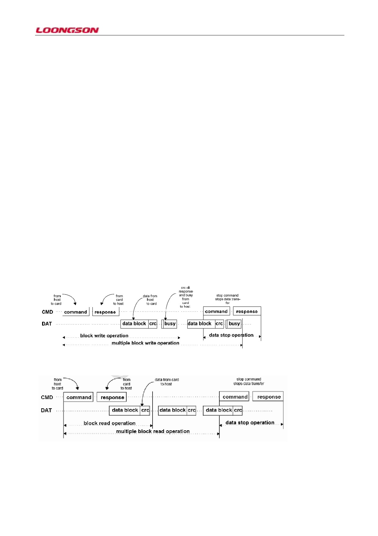
SDIO is a serial communication method, and master and slave devices can implement the transmission of data and
status by message delivery. The below is the schematic diagram of writing multi-block data, and its process is as
follows:
1. The master device sends the write command message to salve device by order wire.
2. After the slave device receives the message, it sends the acknowledgment message to slave device by order line.
3. After the master device receives the right acknowledge message, a data block (512K Byte or more) are sent to
the slave device by data line and to test the busy status of data line.
2. After the slave device receives the right data, it enters into the programming state. Then, the data line is set to
busy, and won’t respond to the data request of master device.
5. From the master device detection to device programming, the next data block will be sent continuously.
6. After the master device sends the last data block, it sends the stop command to the slave device by command
line. After the slave device receives the right response, the multi-block read and write operations are finished.
Figure 22-1 Schematic diagram of SD card multi-block write operation
The multi-block read operation is similar with the multi-block write operation (supplementary instructions).
Figure 22-2 Schematic diagram of SD card multi-block read operation
Different commands have a uniform format. The format of general commands is shown in the table below, 1bit
start bit, 1bit transmission direction bit, 6bit command sequence number, 32bit command parameter, 7bit CRC
check bit and 1bit stop bit.
-176-
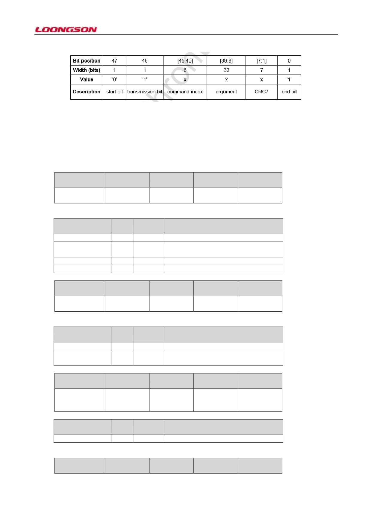
Table 22-1 Command format in SD mode
Therein, the command index corresponds to the command number, for example, cmdindex is 0 for command 0,
and cmdindex is 37 for command 55. Parameters of different commands may be different. Please refer to SD
protocol specification
22.3 Register Description
The register of SDIO controller is shown as follows:
Register name
Address
Read / Write
Function
Reset value
(R / W)
description
sdi_con
0xbfe6c000
r/w
SDIO control0x0
register
sdi_con
Bit
Default
Description
values
reserved
31:9
0x0
soft_rst
8
0x0
Software reset, the entire module is reset.
Hardware is automatically cleared after reset
reserved
7:0
0x0
enclk
0
0x0
SD clock output enable
Register name
Address
Read / Write
Function
Reset value
(R / W)
description
sdi_pre
0xbfe6c004
r/w
SDIO prescale0x1
register
sdi_pre
Bit
Default
Description
values
reserved
31:8
0x0
sdi_pre
7:0
0x1
SDIO clock prescale value, the output
frequency =PCLK/prescale value
Register name
Address
Read / Write
Function
Reset value
(R / W)
description
sdi_cmd_arg
0xbfe6c008
r/w
SDIO command0x0
parameter
register
sdi_cmd_arg
Bit
Default
Description
values
sdi_cmd_arg
31:0
0x0
Command parameter
Register name
Address
Read / Write
Function
Reset value
(R / W)
description
-177-