Loongson 1C300 Processor User Manual (Version 1.0, 2014) - page 10
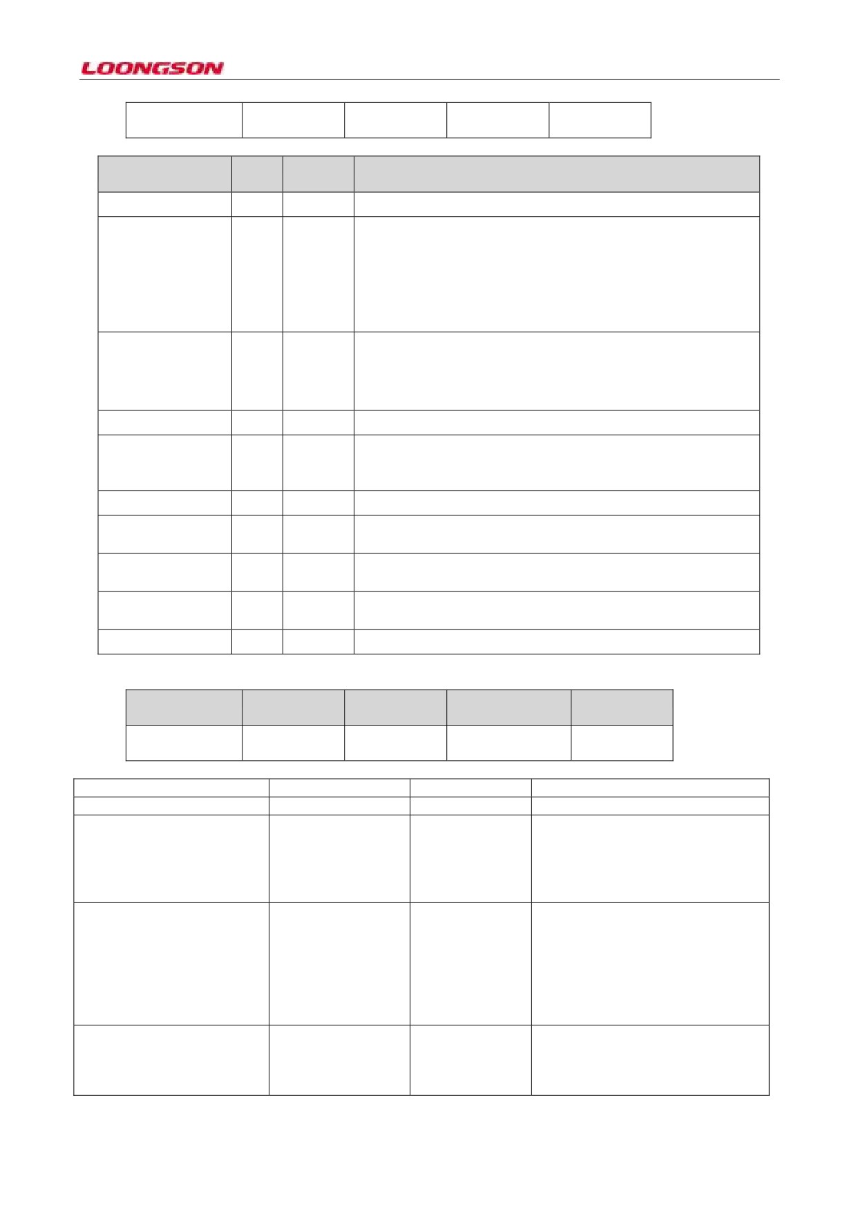
sdi_cmd_con
0xbfe6c00c
r/w
SDIO command0x0
control register
Bit
Default
Description
sdi_cmd_con
values
reserved
31:18
0x0
func_num_abort
17: 15
0x0
When the function number of SDIO card interrupt is used fo
multi-block read and write, the hardware will send the stop
command automatically. If auto_stop_en is
0, this bit is
insignificant.
sdio_en
14
0x0
SDIO enable signal. When used for multi-block read and write, the
hardware will send the stop command automatically. If the bit is 1,
CMD52 is sent; if the bit is 0, CMD12 is sent. If auto_stop_en is 0,
this bit is insignificant.
Check the CRC or not, significant at 1
check_on
13
0x0
Hardware automatically sends a stop command. In multi-block read
auto_stop_en
12
0x0
and write, does the hardware send the stop command
automatically? If the bit is 1, it’s significant.
reserved
11
0x0
Is it the 136-bit long response? If the bit is 1, it’s the long message
long_rsp
10
0x0
reply.
It decides whether the host waits for the response. If the bit is 1, it
wait_rsp
9
0x0
indicates waiting for message reply.
When the bit is set to 1, the command starts, and the hardware is
CMST
8
0x0
cleared automatically after the command ends.
Command index with initial 2 bits (8bits in total)
cmd_index
7:0
0x0
Register name
Address
Read / Write
Function
Reset value
(R / W)
description
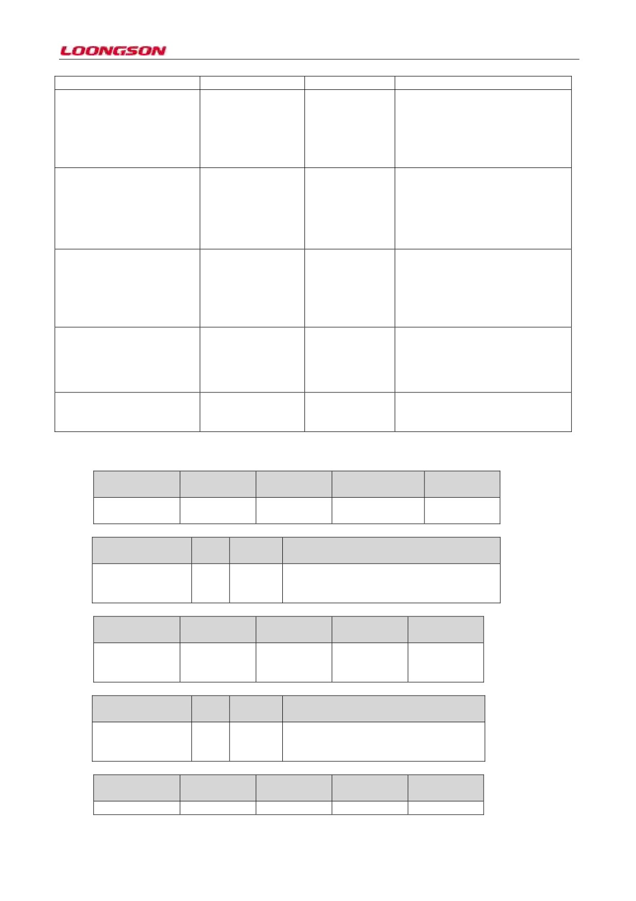
sdi_cmd_sta
0xbfe6c010
ro
SDIO command
0x0
status register
sdi_cmd_sta
Bit
Default value
Description
reserved
31:13
0x0
cmd_sent_fin
14
0x0
Flag bit of the command sending
(including response) finished. When
the bit is
1, it indicates that the
command is sent and the response is
made.
auto_stop
13
0x0
Flag bit of hardware sending stop
command automatically. When the
bit is
1, it indicates that the
hardware sends stop command
automatically, and when it’s
0, it
indicates the hardware sends does
not stop command automatically
rsp_crc_err
12
0x0
Response CRC error. Received
response CRC error. When the bit is
1, it indicates responding CRC
error, and when it’s 0, it indicates no
-178-
CRC error is found.
cmd_end
11
0x0
Command
sending
finished
(indifferent to concern). When the
bit is
1, it indicates command
sending finished, and when it’s 0, it
indicates
command
sending
unfinished.
cmd_tout
10
0x0
Command timeout. Command
response timeout (64 clock periods)
or R1b command, busy waiting
command. When the bit is
1, it
indicates response timeout, and
when it’s 0, it indicates no timeout.
rsp_fin
9
0x0
Response finished, and return
message received from equipment.
When the bit is
1, it indicates
response finished, and when the bit
is
0,
it
indicates
response
unfinished.
cmd_on
8
0x0
Flag bit of command transmission.
When the bit is
1, it indicates
transmission under way, and when
it’s 0, it indicates the transmission is
finished.
rsp_index
7:0
0x0
Response index with initial 2 bits
returned from equipment (8bits in
total)
Register name
Address
Read / Write
Function
Reset value
(R / W)
description
sdi_rsp0
0xbfe6c014
ro
SDIO command0x0
response register 0
sdi_cmd_arg
Bit
Default
Description
values
sdi_rsp0
31:0
0x0
Card status [31:0] (short), card status [127:96]
(long) see sdi_cmd_con[10] for the
configuration of long response
Register name
Address
Read / Write
Function
Reset value
(R / W)
description
sdi_rsp1
0xbfe6c018
ro
SDIO command0x0
response
register 1
sdi_cmd_arg
Bit
Default
Description
values
sdi_rsp1
31:0
0x0
Unused (short), card status [95:64]
(long)
see sdi_cmd_con[10] for the configuration
of long response
Register name
Address
Read / Write
Function
Reset value
(R / W)
description
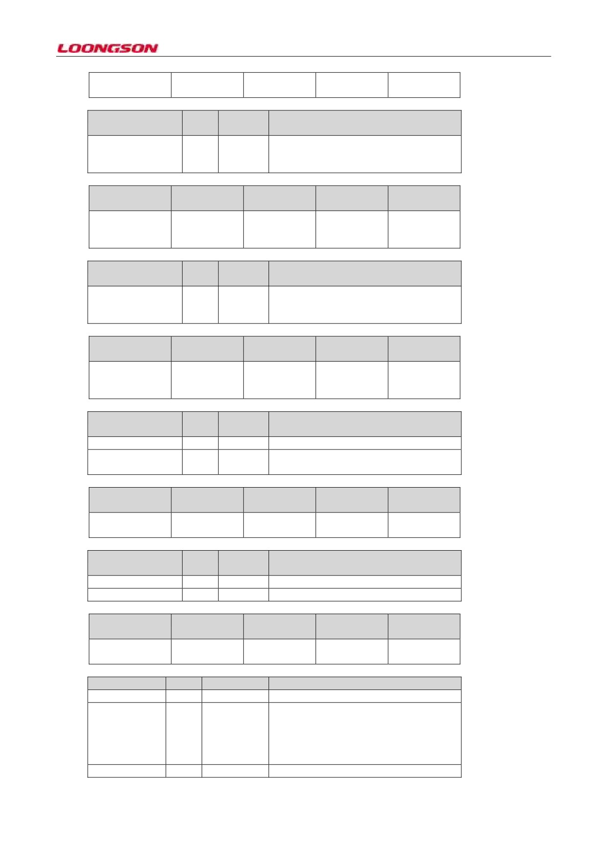
sdi_rsp2
0xbfe6c01c
ro
SDIO command0x0
-179-
response
register 2
sdi_cmd_arg
Bit
Default
Description
values
sdi_rsp2
31:0
0x0
Unused (short), card status [63:32]
(long)
see sdi_cmd_con[10] for the configuration
of long response
Register name
Address
Read / Write
Function
Reset value
(R / W)
description
sdi_rsp3
0xbfe6c020
ro
SDIO command0x0
response
register 3
sdi_cmd_arg
Bit
Default
Description
values
sdi_rsp3
31:0
0x0
Unused (short), card status [31:0] (long) see
sdi_cmd_con[10] for the configuration of
long response
Register name
Address
Read / Write
Function
Reset value
(R / W)
description
sdi_dtimer
0xbfe6c024
r/w
SDIO command0x0
data
timeout
register
sdi_dtimer
Bit
Default
Description
values
reserved
31:24
0x0
sdi_dtimer
23:0
0x0
Data timeout count value uses the clock
count after frequency division
Register name
Address
Read / Write
Function
Reset value
(R / W)
description
sdi_bsize
0xbfe6c028
r/w
SDIO block size
0x0
register
sdi_bsize
Bit
Default
Description
values
reserved
31:23
0x0
sdi_bsize
11:0
0x0
Block size value (0 to 4095)
Register name
Address
Read / Write
Function
Reset value
(R / W)
description
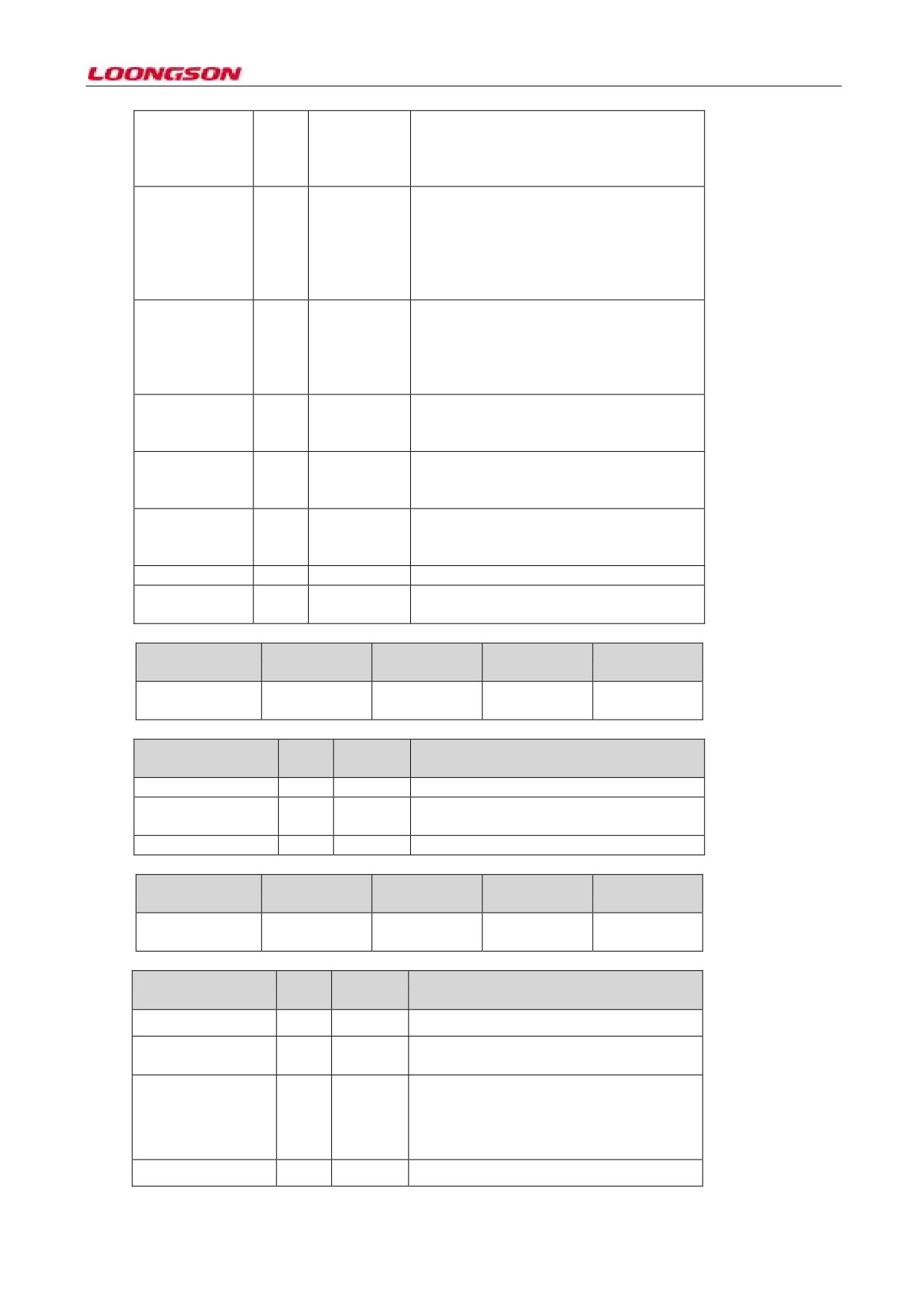
sdi_dat_con
0xbfe6c02c
r/w
SDIO
data0x0
control register
sdi_dat_con
Bit
Default values
Description
reserved
31:15
0x0
resume_rw
20
0x0
SDIO suspend and resume reading and
writing flag bit. When the bit is
1, the
previous write operations are recovered
after SDIO suspension; when the bit is 0,
previous read operations are recovered.
IO_resume
19
0x0
SDIO recovery request. After the SDIO
-180-
device enters into the suspended state, 1 is
written to this bit. After
0 is written to
IO_suspend, SDIO device recovers
previous operations.
IO_suspend
18
0x0
SDIO suspending request. After
1 is
written to this bit, the controller will send
CMD52 command in right time, and notify
SDIO device to enter into the suspended
state. Write 0 in this bit when resuming
operation
RwaitReq
17
0x0
Read pending request After 1 is written to
the bit, the controller will pull down DAT2
in right time, and notify SDIO device to
enter into the read waiting state. Write 0 to
recover the previous read operation.
wide_mode
16
0x0
Bit width select bit. When the bit is 1, it
indicates t he four-wire mode; when the bit
is 0, it indicates the single-line mode.
DMA_en
15
0x0
DMA enable When the bit is 1, it indicates
DMA enable; when the bit is 0, it indicates
DMA disable.
DTST
14
0x0
When 1 is written to the bit, the data
transfer begins, and the hardware is
cleared after the data transfer ends.
reserved
13:12
0x0
blk_num
11:0
0x0
The number of blocks for reading and
writing operations
Register name
Address
Read / Write
Function
Reset value
(R / W)
description
sdi_dat_cnt
0xbfe6c030
r/w
SDIO
data0x0
counter
sdi_dat_cnt
Bit
Default
Description
values
reserved
31:24
0x0
blk_num_cnt
23:12
0x0
Current number of bytes of transmission
blocks
blk_cnt
11:0
0x0
Current number of transmission blocks
Register name
Address
Read / Write
Function
Reset value
(R / W)
description
sdi_dat_sta
0xbfe6c034
ro
SDIO
data0x0
status register
Bit
Default
Description
sdi_dat_sta
values
reserved
31:11
0x0
When the bit is 1, it indicates in suspended
suspend_on
16
0x0
status.
rst_suspend
15
0x0
When the bit is 1, it indicates .in suspended
reset After the SDIO device is suspended,
the controller resets FIFO and DMA
requests.
When the bit is 1, it indicates R1b
R1b_tout
14
0x0
-181-
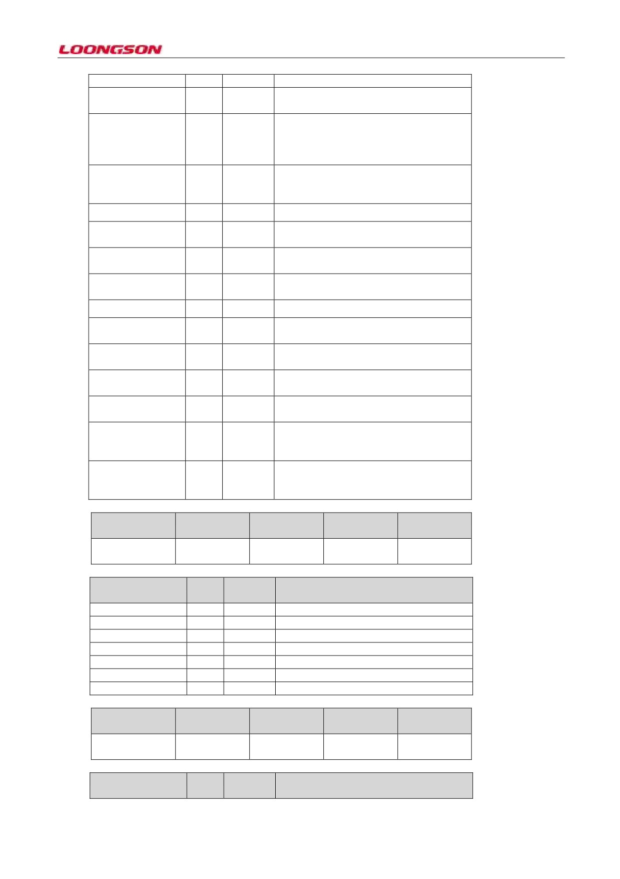
command timeout.
When the bit is 1, it indicates data
data_start
13
0x0
transmission starting
Test the completion of the command with
R1b_fin
12
0x0
busy state When the command with busy
state is sent, the bit is 0; when the busy
state ends, the bit becomes 1.
When the bit is 1, it indicates the hardware
auto_stop
11
0x0
is sending the stop command
automatically.
reserved
10
0x0
Reading waiting to happen. Send the read
r_wait_req
9
0x0
waiting request signal to SDIO card.
SDIO interrupt flag bit. When the bit is 1,
SDIO_int
8
0x0
it indicates interrupt detection
After the data transfer, CRC error is
crc_sta
7
0x0
returned from the device
Data receiving CRC errors
dat_crc
6
0x0
Data transmission timeout. When the bit is
dat_tout
5
0x0
1, it indicates data timeout
Data transmission end flag bit. When the
dat_fin
4
0x0
bit is 1, it indicates data transmission end
Busy end flag bit (such as programming).
busy_fin
3
0x0
When the bit is 1, it indicates busy end
Programming error flag bit. When the bit is
prog_err
2
0x0
1, it indicates the wrong programming.
In Tx data transfer, when the bit is 1, it
tx_dat_on
1
0x0
indicates sending; when the bit is 0, it
indicates sending completes.
In rX data acceptance, when the bit is 1, it
indicates receiving; when the bit is 0, it
rx_dat_on
0
0x0
indicates receiving completes.
Register name
Address
Read / Write
Function
Reset value
(R / W)
description
sdi_fifo_sta
0xbfe6c038
ro
SDIOFIFO
0x0
Status register
sdi_fifo_sta
Bit
Default
Description
values
reserved
31:12
0x0
tx_full
11
0x0
tx fifo full flag bit
tx_empty
10
0x0
tx fifo empty flag bit
reserved
9
0x0
rx_full
8
0x0
rx fifo full flag bit
rx_empty
7
0x0
rx fifo empty flag bit
reserved
6:0
0x0
Register name
Address
Read / Write
Function
Reset value
(R / W)
description
sdi_int_msk
0xbfe6c03c
r/c
SDIO interrupt0x0
register
sdi_int_msk
Bit
Default
Description
values
-182-
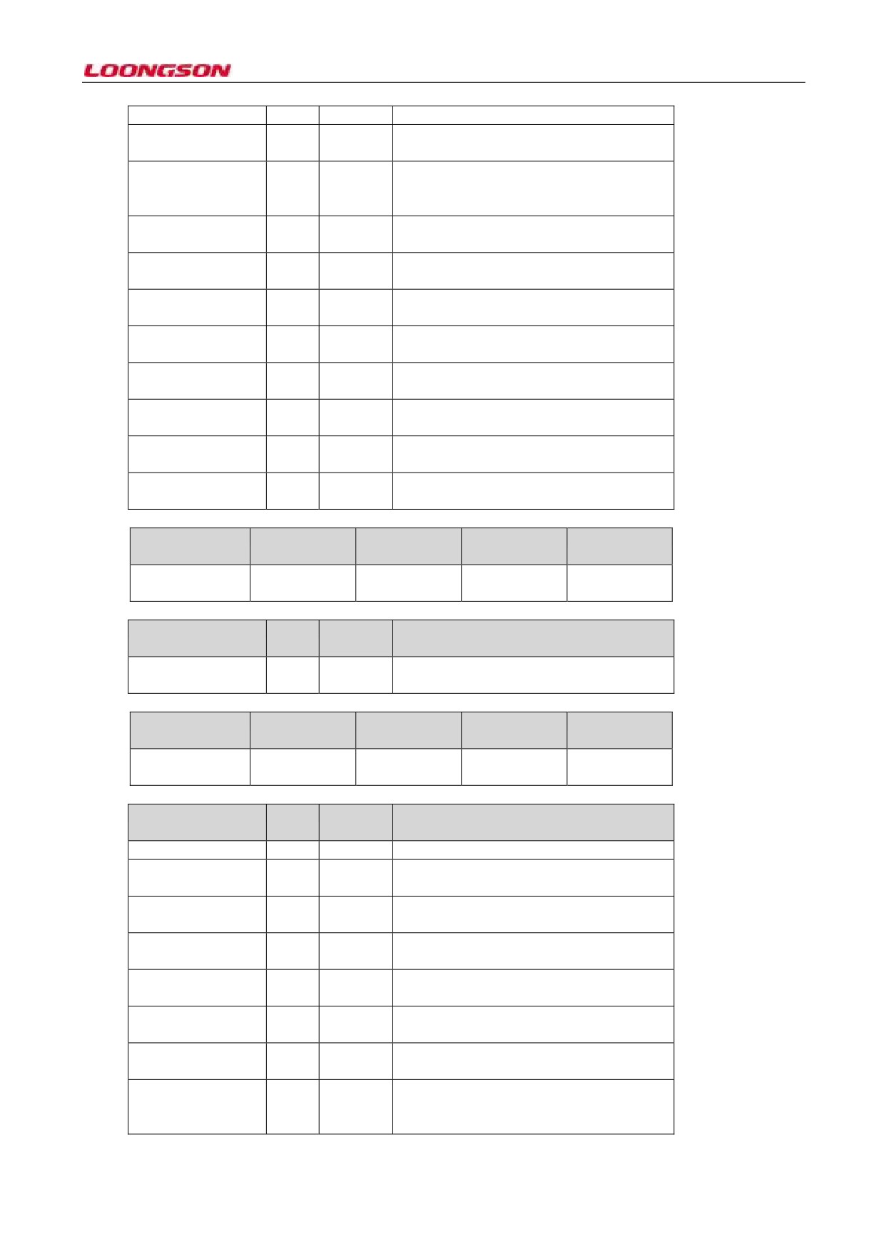
reserved
31:10
0x0
R1b_fin_int
9
0x0
Detest busy end interrupt, 1 is written to
the bit for clearing.
rsp_crc_int
8
0x0
The command responds to CRC error
interrupt, and
1 is written to the bit for
clearing.
cmd_tout_int
7
0x0
Command timeout interrupt, 1 is written to
the bit for clearing.
cmd_fin_int
6
0x0
Number of command transmission
completion interrupt, hardware clearing
SDIO_int
5
0x0
Detest SDIO interrupt, and 1 is written to
the bit for clearing.
prog_err_int
4
0x0
SD card programming error interrupt, and
1 is written to the bit for clearing
crc_sta_int
3
0x0
After the data is sent, CRC error interrupt
is returned from device, write 1 and clear
dat_crc_int
2
0x0
The data receives CRC error interrupt,
write 1 and clear
dat_tout_int
1
0x0
Data timeout interrupt, and 1 is written to
the bit for clearing
dat_fin_int
0
0x0
Data interrupt completion, hardware
clearing
Register name
Address
Read / Write
Function
Reset value
(R / W)
description
sdi_dat
0xbfe6c040
ro
SDIO command0x0
data register
sdi_dat
Bit
Default
Description
values
SDIO controller sends or receives data (used
sdi_dat
31:0
0x0
DMA operation)
Register name
Address
Read / Write
Function
Reset value
(R / W)
description
sdi_int_en
0xbfe6c064
r/w
SDIO interrupt0x0
enable register
sdi_int_en
Bit
Default
Description
values
reserved
31:10
0x0
R1b_fin_int_en
9
0x0
Busy finish interrupt enable. When the bit
is 1, it’s significant.
Command response CRC error interrupt
rsp_crc_int_en
8
0x0
enable. When the bit is 1, it’s significant.
cmd_tout_int_en
7
0x0
Command timeout interrupt enable,
significant at 1
cmd_fin_int_en
6
0x0
Data command send finish interrupt
enable. When the bit is 1, it’s significant.
SDIO_int_en
5
0x0
SDIO interrupt enable. When the bit is 1,
it’s significant.
prog_err_int_en
4
0x0
SD card programming error interrupt
enable. When the bit is 1, it’s significant.
crc_sta_int_en
3
0x0
Return CRC error interrupt enable after the
data transfer. When the bit is
1, it’s
significant.
-183-
dat_crc_int_en
2
0x0
Data receive CRC error interrupt enable.
When the bit is 1, it’s significant.
dat_tout_int_en
1
0x0
Data timeout interrupt enable, significant
at 1
dat_fin_int_en
0
0x0
Data completion interrupt
enable,
significant at 1
22.4 Software Programming Instructions
22.4.1 SD Memory card software programming instructions
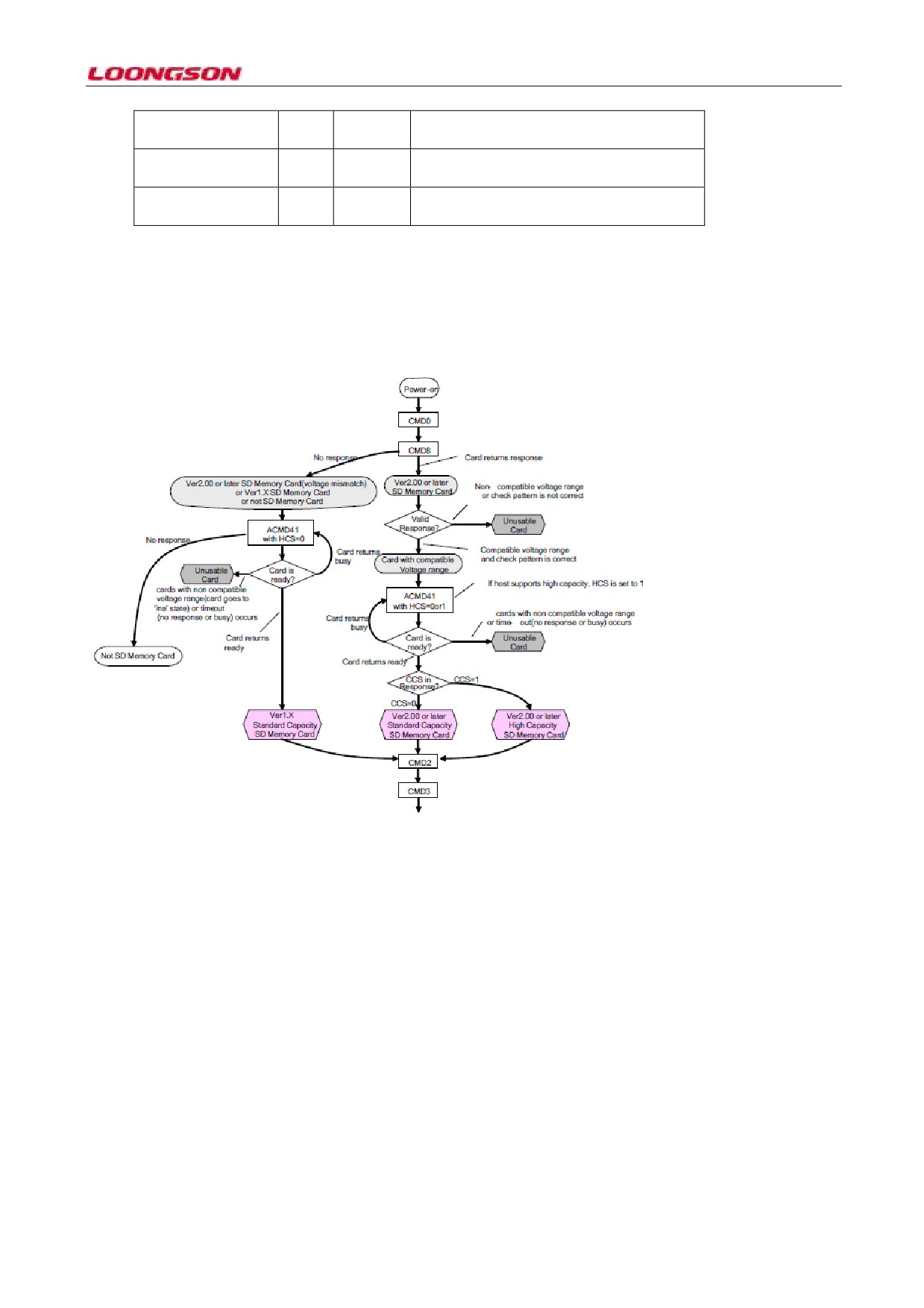
If SD Memory card wants to operate normally, it must be initialized first. The initialization process needs to send
different command sequences to configure the slave device. Initialization process diagram as follows:
Figure 22-3 Schematic diagram of SD Memory card initialization process
Normal work can be carried out after initialization completion.
Configuration register process is as follows:
1. Configure sdi_con, enable output clock
2. Configure sdi_pre, set a frequency division factor, and if the time sequence isn’t satisfied, the output direction
clock is set to adjust the time sequence.
3. Configure sdi_int_en, enable command and data completion and other interrupts.
4. According to the above initialization process, the configuration register where initialization controller sends
command as follows:
¾ Based on the sent command, the cmd_arg register is configured.
¾ Configure cmd_con register, send command
¾ Read sdi_int_msk register, and check if the transfer is finished, and if there is an error
¾ If necessary, read the sdi_rsp register
Initialization process is as follows:
CMD0ĺCMD8ĺACMD41(namely, CMD55ĺCMD41) ĺCMD2ĺCMD3ĺCMD7ĺACMD6 (if 4bit data line
is used for transfer)
5. Before the data operation, it’s necessary to configure Bsize register and Dtimer register.
-184-
6. For the data operation, it’s necessary to configure DMA, configure dat_con register and DMA (Notes: In read
operation, configure DMA first, and in write operation, configure dat_con first)
7. Read sdi_int_msk register, and check if the transfer is finished, and if there is an error
8. Without error, one data transfer is finished, and it doesn’t need the software to send stop command.
22.4.2 SDIO card software programming instructions
The initialization process of SDIO card is different from that of SD memory card, and it’s initialized as follows:
1.
Configure sdi_con, enable output clock
2.
Configure sdi_pre, set one frequency division factor. If the time sequence isn’t satisfied, the output inversion
is set.
3.
Clock to adjust timing sequence.
4.
Configure sdi_int_en, enable command and data completion and other interrupts.
5.
Initialization process is as follows: Configuration register process for transmitting command is as follows:
¾
Based on the sent command, the cmd_arg register is configured.
¾
Configure cmd_con register, send command
¾
Read sdi_int_msk register, and check if the transfer is finished, and if there is an error
¾
If necessary, read the sdi_rsp register
The initialization process is shown as follows (the CCCR operation)
6.
CMD52 (reset) ĺCMD5 (after powered on) ĺCMD3 (obtain RCA) ĺCMD7 (select the corresponding
RCA card) ĺCMD52 (configure whether to use 4bit data line transmission) ĺCMD52 (configure the block
size of read and write data) ĺCMD52 (open IO interrupt enable) it’s necessary to configure Bsize register
and Dtimer register before row data operation.
7.
For the data operation, it’s necessary to configure DMA, configure dat_con register and DMA (Notes: In read
operation, configure DMA first, and in write operation, configure dat_con first)
8.
In sending the command of read and write data, if the hardware is required to send stop command
automatically, it’s necessary to configure auto_stop and sdio_en. In reading and writing data, it’s necessary to
read and write Function, configure the corresponding FBR pointer register, and then send multi-block read
and write (CMD53) or single-block read and write (CMD52) command to read and write.
9.
Read sdi_int_msk register, and check if the transfer is finished, and if there is an error
10. Without error, one data transfer is finished, and it doesn’t need the software to send stop command.
11. If the IO interrupt is detected, the controller will enable the interrupt triggering response, but will not stop the
current operation.
12. For the read waiting, the controller will pull down DAT2 in right time, and notify the SDIO card to stop
sending data. Thus, if it’s under the process of data transfer, the controller may send the wait signal after the
previous data block transfer ends, and it won’t receive the next block data.
13.
13 For the suspending and resuming operations. Suspend and nest may occur, for example, operation 1 is
suspended because operation 2 interrupts, and then operation 2 is suspended because operation 3 interrupts.
In suspension, the interrupt field requires the software to save( such as read and write flag bit, number of
current transmission block, address and so on), and starts the PUSH operation. In recovery, the software is
pulled in corresponding sequence.
-185-
23 CAN Controller
23.1 Overview
1C integrates two ways of CAN interface controllers CAN bus is the serial bus made up of transmitter data line
TX and receiver data line RX to transmit and receive data. The bidirectional transfer is conducted between devices,
and the highest transfer rate is 1Mbps
The interrupt of two CAN bus controllers is connected to the first group of interrupt control registers. Therein,
can0 interrupt corresponds to bit6, and can1 interrupt to bit7. Refer to description in Chapter 15.
The register base address of CAN0 bus controller is 16KB at the beginning of 0xbfe5_0000.
The register base address of CAN1 bus controller is 16KB at the beginning of 0xbfe5_4000.
23.2 CAN Controller Architecture
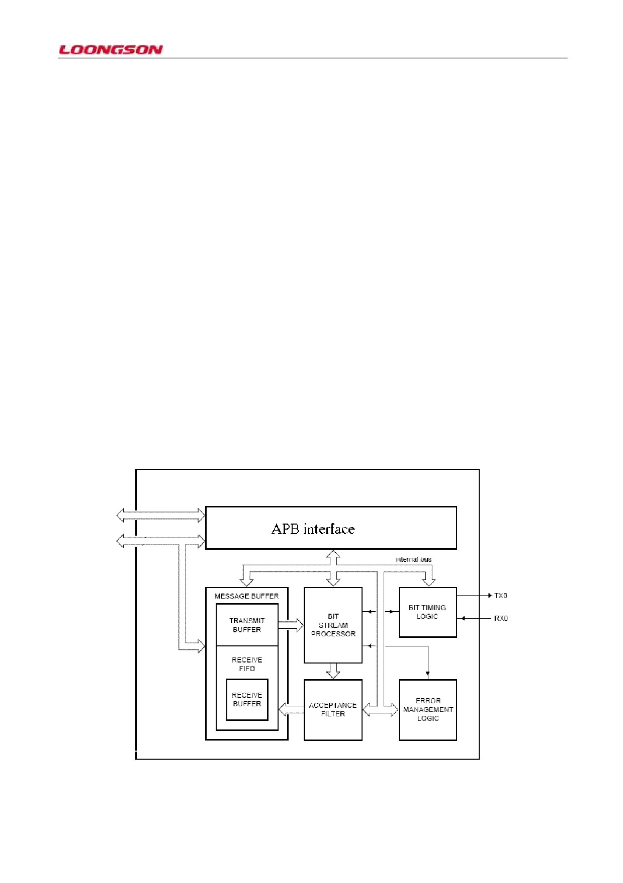
The figure below is the architecture of CAN master controller, and main modules include APB bus interface, bit
stream processing unit, bit time sequence logic, error management logic, receiving filtering, and data buffer cache.
z
APB bus interface: receive APB bus command and return data.
z
Bit stream processing unit: implement the control of data stream between transmitter buffer, receiver FIFO
and CAN bus, and performs functions such as error detection, bus arbitration, data filling and error handling.
z
Bit time sequence logic: monitor the serial CAN bus and handle the bit time sequence related to the bus. In
addition, it provides the programmable time quantum to compensate the propagation delay time, phase switch
(for example, due to oscillation drift) and define the sampling point and sampling times within the time of
one bit.
z
Error management logic: judge the transmitted CRC error and count errors.
z
Receiving filtering: compared the received identification codes to decide whether to receive the message or
not.
z
Data buffer cache: the receiving buffer is the interface between acceptance filter and CPU, and is also used to
store messages received from CAN bus. As one window of FIFO (64 bytes long) , the receive buffer (13
bytes) may be accessed by CPU.
Figure 23-1 CAN master controller architecture
-186-
CAN supports two operating modes: standard mode and expansion mode. The operating mode is selected through
CAN mode in command register. Reset default is the standard mode.
23.3 Standard Mode
23.3.1 Standard mode address list
The address area includes the control segment and message buffer. In initial loading, the control segment may be
programmed to configure communication parameters, and the message to be transmitted will be written in send
buffer. After receiving the message, the microcontroller will read the received message from receive buffer, and
then release the space for next application.
After the initial loading, the acceptance code and acceptance mask of register, 0 and 1 of bus timing register, and
output control can’t be changed. Only when the reset bit of control register is set high, can these registers be
accessed. In different modes of reset mode and operating mode, the access register is different. After the hardware
reset or controller drops, the bus status of status register will enter into the reset mode automatically. The operating
mode is activated by the reset request of setting control register.
CAN
field
Operating mode
Reset mode
address
Read
Write
Read
Write
0
Control
Control
Control
Control
1
FF
Commands
FF
Commands
2
Status
-
Status
-
3
FF
-
Interrupt
-
Control
4
FF
-
Acceptance code
Acceptance
code
5
FF
-
Acceptance mask
Acceptance
mask
6
FF
-
Bus timing 0
Bus timing 0
7
FF
-
Bus timing 1
Bus timing 1
8
Reserved
Reserved
Reserved
Reserved
9
Reserved
Reserved
Reserved
Reserved
10
ID (10-3)
ID (10-3)
FF
-
ID
(2-0), RTR,ID
(2-0), RTR,
11
DLC
DLC
FF
-
12
Data byte 1
Data byte 1
FF
-
13
Data byte 2
Data byte 2
FF
-
14
Data byte 3
Data byte 3
FF
-
15
Data byte 4
Data byte 4
FF
-
16
Data byte 5
Data byte 5
FF
-
17
Data byte 6
Data byte 6
FF
-
18
Data byte 7
Data byte 7
FF
-
19
Data byte 8
Data byte 8
FF
-
20
ID (10-3)
ID (10-3)
FF
-
ID
(2-0), RTR,ID
(2-0), RTR,
21
DLC
DLC
FF
-
22
Data byte 1
Data byte 1
FF
-
23
Data byte 2
Data byte 2
FF
-
24
Data byte 3
Data byte 3
FF
-
25
Data byte 4
Data byte 4
FF
-
26
Data byte 5
Data byte 5
FF
-
27
Data byte 6
Data byte 6
FF
-
28
Data byte 7
Data byte 7
FF
-
29
Data byte 8
Data byte 8
FF
-
-187-
23.3.2 Control register (CTR)
English name: control register
Register bit width: [7:0]
Offset: 0x00
Reset value: 0x01
The reading value of this bit is always logic 1. In hard boot or when the bus status bit set to 1 (bus shutdown), the
reset request bit is set to 1. If these bits are accessed by software, its value will change and influence the next
rising edge of the internal clock. During the external reset, the microprocessor can’t set the reset request bit to 0. If
the reset request bit is set to 0, the microprocessor must check the bit and guarantee the external reset pin isn’t low.
The change in reset request bit is synchronous with internal frequency division clock. Read reset request bit, and
you can find such synchronous state.
After the reset request bit is set to 0, the controller will wait.
a) One bus idle signal (11 weak bit), if the previous reset request is hardware rest or CPU initial reset.
b) 128 buses are idle, if the previous reset request is caused by initialization bus before CAN controller reenters
the bus startup mode.
Bit field
Bit field name
Bit width
Access
Description
7: 5
Reserve
3
-
Reserved
4
OIE
1
Rw
Overflow interrupt enable
3
EIE
1
Rw
Error interrupt enable
2
TIE
1
Rw
Transmit interrupt enable
1
RIE
1
Rw
Receive interrupt enable
0
RR
1
Rw
Reset request
23.3.3 Command register (CMR)
English name: Command register
Register bit width: [7:0]
Offset: 0x01
Reset value: 0x00
For microcontroller, the command register is the write-only memory, and if the address is read, the returned value
is 1111 1111.
Bit field
Bit field name
Bit width
Access
Description
7
EFF
1
W
Extension mode
6: 5
Reserve
2
-
Reserved
4
GTS
1
W
sleep
3
CDO
1
W
Clear data overflow
2
RRB
1
W
Release receiving buffer
1
AT
1
W
Stop transmitting
0
TR
1
W
RTS (Request to send )
23.3.4 Status register (SR)
English name: Status register
Register bit width: [7:0]
Offset: 0x02
Reset value: 0x00
Bit field
Bit field name
Bit width
Access
Description
7
BS
1
R
Bus status
-188-
6
ES
1
R
Faulted state
5
TS
1
R
Send state
4
RS
1
R
Receive state
3
TCS
1
R
Send completed state
2
TBS
1
R
Transmit buffer state
1
DOS
1
R
Data overflow state
0
RBS
1
R
Receive buffer status
23.3.5 Interrupt register (IR)
English name: Interrupt register
Register bit width: [7:0]
Offset: 0x03
Reset value: 0x00
Bit field
Bit field name
Bit width
Access
Description
7: 5
Reserved
1
R
Reserved
4
WUI
1
R
Wake-up interrupt
3
DOI
1
R
Data overflow interrupt
2
EI
1
R
Error interrupt
1
TI
1
R
Send interrupt
0
RI
1
R
Receive interrupt
23.3.6 Acceptance Code Register (ACR)
English name: Acceptance code register
Register bit width: [7:0]
Offset: 0x04
Reset value: 0x00
In reset, the register may be read and written.
Bit field
Bit field name
Bit width
Access
Description
7:0
AC
8
RW
ID acceptance code
23.3.7 Acceptance Mask Register (AMR)
English name: Acceptance mask register
Register bit width: [7:0]
Offset: 0x05
Reset value: 0x00
Acceptance code bit AC is equal to high 8bits ID.10-ID.3 of message identification code, and when it corresponds
to the phase of acceptance mask bit or is 1, the data may be accepted. In reset, the register may be read and
written.
Bit field
Bit field name
Bit width
Access
Description
7:0
AM
8
Rw
ID mask bit
23.3.8 Transmit buffer list
The buffer is used to store the message that the microprocessor requires CAN controller to send, and it’s divided
into descriptor area and data area. The read/write of buffer can only be sent by microcontroller in operating mode,
and in reset mode the read value is always FF.
Address
Area
Name
Data bit
10
ID byte 1
ID (10-3)
-189-

ID byte 2
ID (2-0), RTR, DLC
11
12
TX data 1
TX data 1
13
TX data 2
TX data 2
14
TX data 3
TX data 3
15
TX data 4
TX data 4
16
TX data 5
TX data 5
17
TX data 6
TX data 6
18
TX data 7
TX data 7
19
TX data 8
TX data 8
23.3.9 Receive buffer list
The configuration of receive buffer and send buffer is the same, but the address is changed to 20-29.
23.4 Extension Mode
23.4.1 Extension mode address table
Operating mode
Reset mode
CAN
Read
Write
Read
Write
address
0
Control
Control
Control
Control
1
0
Commands
0
Commands
2
Status
-
Status
-
3
Interrupt
-
Interrupt
-
4
Interrupt enable
Interrupt enable
Interrupt enable
Interrupt enable
5
-
-
Acceptance mask
Acceptance mask
6
Bus timing 0
-
Bus timing 0
Bus timing 0
7
Bus timing 1
-
Bus timing 1
Bus timing 1
8
Reserved
Reserved
Reserved
Reserved
9
Reserved
Reserved
Reserved
Reserved
10
Reserved
Reserved
Reserved
Reserved
11
Arbitration lost capture
-
Arbitration
lost-
capture
12
Error code capture
-
Error code capture
-
13
Error alarm limit
-
Error alarm limit
-
14
RX error counter
-
RX error counter
-
15
TX error counter
-
TX error counter
-
16
RX frame information
TX
frame
Acceptance Code 0
Acceptance Code 0
information
17
RX ID 1
TX ID 1
Acceptance Code 1
Acceptance Code 1
18
RX ID 2
TX ID 2
Acceptance Code 2
Acceptance Code 2
19
RX ID 3
TX ID 3
Acceptance Code 3
Acceptance Code 3
20
RX ID 4
TX ID 4
Acceptance mask 0
Acceptance mask 0
21
RX data 1
TX data 1
Acceptance mask 1
Acceptance mask 1
22
RX data 2
TX data 2
Acceptance mask 2
Acceptance mask 2
23
RX data 3
TX data 3
Acceptance mask 3
Acceptance mask 3
24
RX data 4
TX data 4
-
-
25
RX data 5
TX data 5
-
-
26
RX data 6
TX data 6
-
-
27
RX data 7
TX data 7
-
-
28
RX data 8
TX data 8
-
-
-190-
29
RX message counter
-
RX message counter
-
23.4.2 Mode register (MOD)
English name: Mode register
Register bit width: [7:0]
Offset: 0x00
Reset value: 0x01
The reading value of this bit is always logic 1. In hard boot or when the bus status bit set to 1 (bus shutdown), the
reset request bit is set to 1. If these bits are accessed by software, its value will change and influence the next
rising edge of the internal clock. During the external reset, the microprocessor can’t set the reset request bit to 0. If
the reset request bit is set to 0, the microprocessor must check the bit and guarantee the external reset pin isn’t low.
The change in reset request bit is synchronous with internal frequency division clock. Read reset request bit, and
you can find such synchronous state.
After the reset request bit is set to 0, the controller will wait.
a) One bus idle signal (11 weak bit), if the previous reset request is hardware rest or CPU initial reset.
b) 128 buses are idle, if the previous reset request is caused by initialization bus before CAN controller reenters
the bus startup mode.
Bit field
Bit field name
Bit width
Access
Description
7: 5
Reserve
3
-
Reserved
4
SM
1
Rw
Sleep mode
3
AFM
1
Rw
Single / Dual filter mode
2
STM
1
Rw
Normal operating mode
1
LOM
1
Rw
Listen mode
0
RM
1
Rw
Reset mode
23.4.3 Command register (CMR)
English name: Command register
Register bit width: [7:0]
Offset: 0x01
Reset value: 0x00
For microcontroller, the command register is the write-only memory, and if the address is read, the returned value
is 1111 1111.
Bit field
Bit field name
Bit width
Access
Description
7
EFF
1
W
Extension mode
6: 5
Reserve
2
-
Reserved
4
SRR
1
W
Self receiving request
3
CDO
1
W
Clear data overflow
2
RRB
1
W
Release receiving buffer
1
AT
1
W
Stop transmitting
0
TR
1
W
RTS (Request to send )
23.4.4 Status register (SR)
English name: Status register
Register bit width: [7:0]
Offset: 0x02
Reset value: 0x00
-191-
Bit field
Bit field name
Bit width
Access
Description
7
BS
1
R
Bus status
6
ES
1
R
Faulted state
5
TS
1
R
Send state
4
RS
1
R
Receive state
3
TCS
1
R
Send completed state
2
TBS
1
R
Transmit buffer state
1
DOS
1
R
Data overflow state
0
RBS
1
R
Receive buffer status
23.4.5 Interrupt register (IR)
English name: Interrupt register
Register bit width: [7:0]
Offset: 0x03
Reset value: 0x00
Bit field
Bit field name
Bit width
Access
Description
7
BEI
1
R
Bus error interrupt
6
ALI
1
R
Arbitration lost interrupt
5
EPI
1
R
Error passive interrupt
4
WUI
1
R
Wake-up interrupt
3
DOI
1
R
Data overflow interrupt
2
EI
1
R
Error interrupt
1
TI
1
R
Send interrupt
0
RI
1
R
Receive interrupt
23.4.6 Interrupt enable register (IER)
English name: Interrupt enable register
Register bit width: [7:0]
Offset: 0x04
Reset value: 0x00
Bit field
Bit field name
Bit width
Access
Description
7
BEIE
1
RW
Bus error interrupt enable
6
ALIE
1
RW
Arbitration lost interrupt enable
5
EPIE
1
RW
Error passive interrupt enable
4
WUIE
1
RW
Wake-up interrupt enable
3
DOIE
1
RW
Data overflow interrupt enable
2
EIE
1
RW
Error interrupt enable
1
TIE
1
RW
Transmit interrupt enable
0
RIE
1
RW
Receive interrupt enable
23.4.7 Arbitration Loss Capture Register (IER)
English name: Arbitration lost capture register
Register bit width: [7:0]
Offset: 0xB
Reset value: 0x00
-192-
Bit field
Bit field name
Bit width
Access
Description
7: 5
-
3
R
Reserved
4
BITNO4
1
R
Fourth bit
3
BITNO3
1
R
Third bit
2
BITNO2
1
R
Second bit
1
BITNO1
1
R
First bit
0
BITNO0
1
R
Zero bit
Bit
Decimal
Function
value
0
0
0
0
0
0
Arbitration lost in the ID code bit1
0
0
0
0
1
1
Arbitration lost in the ID code bit 2
0
0
0
1
0
2
Arbitration lost in the ID code bit3
0
0
01
1
3
Arbitration lost in the ID code bit4
0
0
1
0
0
4
Arbitration lost in the ID code bit5
0
0
1
0
1
5
Arbitration lost in the ID code bit6
0
0
1
1
0
6
Arbitration lost in the ID code bit7
0
0
1
1
1
7
Arbitration lost in the ID code bit8
0
1
0
0
0
8
Arbitration lost in the ID code bit9
0
1
0
0
1
9
Arbitration lost in the ID code bit10
0
1
0
1
0
10
Arbitration lost in the ID code bit11
0
1
0
1
1
11
Arbitration lost in SRTR bit
0
1
1
0
0
12
Arbitration lost in IDE bit
0
1
1
0
1
13
Arbitration lost in the ID code bit12
0
1
1
1
0
14
Arbitration lost in the ID code bit13
0
1
1
1
1
15
Arbitration lost in the ID code bit14
1
0
0
0
0
16
Arbitration lost in the ID code bit15
1
0
0
0
1
17
Arbitration lost in the ID code bit16
1
0
0
1
0
18
Arbitration lost in the ID code bit17
1
0
0
1
1
19
Arbitration lost in the ID code bit18
1
1
1
0
0
20
Arbitration lost in the ID code bit19
1
1
1
0
1
21
Arbitration lost in the ID code bit 20
1
1
1
1
0
22
Arbitration lost in the ID code bit21
1
1
1
1
1
23
Arbitration lost in the ID code bit22
1
0
0
0
0
24
Arbitration lost in the ID code bit 23
1
0
0
0
1
25
Arbitration lost in the ID code bit 24
1
0
0
1
0
26
Arbitration lost in the ID code bit 25
1
0
0
1
1
27
Arbitration lost in the ID code bit26
1
1
1
0
0
28
Arbitration lost in the ID code bit 27
1
1
1
0
1
29
Arbitration lost in the ID code bit 28
1
1
1
1
0
30
Arbitration lost in the ID code bit 29
1
1
1
1
1
31
Arbitration lost in RTR bit
23.4.8 Error Alarm Limit Register (EMLR)
English name: Error alarm limit register
Register bit width: [7:0]
Offset: 0xD
Reset value: 0x60
Bit field
Bit field name
Bit width
Access
Description
[7:0]
EML
8
Rw
Error alarm threshold
-193-
23.4.9 RX Error Count Register (RXERR)
English name: RX error count register
Register bit width: [7:0]
Offset: 0xE
Reset value: 0x60
Bit field
Bit field name
Bit width
Access
Description
[7:0]
RXERR
8
R
Receive error count
23.4.10 TX Error Count Register (TXERR)
English name: TX error count register
Register bit width: [7:0]
Offset: 0xF
Reset value: 0x60
Bit field
Bit field name
Bit width
Access
Description
[7:0]
TXERR
8
R
Transmit error count
23.4.11 Acceptance filter
With the help of acceptance filter, only when the value predefined by identification bit and acceptance filter in
received message are equal, can CAN controller be allowed to store the received message into RXFIFO. The
acceptance filter is defined by acceptance code register and acceptance mask register. In mode register, the single
filter mode or double filter mode is selected. See SJA1000 data manual for the specific configuration.
23.4.12 RX message count register (RMCR)
English name: RX message count register
Register bit width: [7:0]
Offset: 0x1 D
Reset value: 0x00
Bit field
Bit field name
Bit width
Access
Description
[7:0]
RMCR
8
R
The received data frame counter
23.5 Public Register
23.5.1 Bus timing register 0 (BTR0)
English name: Bus timing register
Register bit width: [7:0]
Offset: 0x06
Reset value: 0x00
Notes: in reset mode, it’s read and written; in operating mode, it’s read-only.
Bit field
Bit field name
Bit width
Access
Description
7: 6
SJW
8
RW
Synchronization skip width
[5£º0]
BRP
8
RW
The Baud rate frequency division factor
23.5.2 Bus timing register 1 (BTR1)
English name: Bus timing register 1
Register bit width: [7:0]
Offset: 0x07
-194-
Reset value: 0x00
Bit field
Bit field name
Bit width
Access
Description
7
SAM
1
Rw
When the bit is 1, it’s sampled three times, or
sampled once.
6: 4
TESG2
3
Rw
The count value of time period 2 in a bit
3:0
TSEG1
4
Rw
The count value of time period 2 in a bit
23.5.3 Output Control Register (OCR)
English name: Output control register
Register bit width: [7:0]
Offset: 0x08
Reset value: 0x00
Bit field
Bit field name
Bit width
Access
Description
[7:0]
OCR
8
Rw
Reserved
-195-
24 ADC Controller
24.1 Overview
Loongson 1C integrates the ADC controller that is used to control ADC channel and has implemented some
specific applications, such as continuous switch, single switch, touch screen application and analog watchdog.
Main characteristic parameters of ADC controller in Loongson 1C include:
z
4-channel ADC analog input, 10bit output precision
z
Measuring voltage scope is 0.01~0.99VREF, and recommend the VREF input of 0.5~0.9VDDA
z
The operating frequency of ADC can be configured from 0 to 16M
z
The operating mode of ADC has single and continuous switch, and the touch screen application belong to the
special continuous switch.
z
The continuous conversion of ADC adopts DMA transmission data, but the coordinates of touch screen
doesn’t adopt DMA.
z
The continuous conversion interval of ADC can be configured from 0 to 1M.
z
In continuous switch, the unused channels of ADC may conduct the single switch.
z
In touch screen application, when the touch screen is pressed, the interrupt is generated; when the touch
screen is released, the interrupt is also generated.
z
It can support four-wire touch screen and five-wire touch screen. In the connection of four-wire touch screen,
two ways of general ADC may be used. In the connection of five-wire touch screen, three ways of general
ADC may be used.
z
Support multi-channel scanning single conversion
z
It supports the function of analog watchdog, and the upper and lower thresholds may be configured. And the
interrupt is generated when exceeding the threshold.
24.2 Register Description
Register name
Address
Read / Write
Function
Reset value
(R / W)
description
adc_cnt
0xbfe74000
R/W
Frequency
0x400010
division
and
sampling
interval register
Adc_cnt
Bit
Default
Description
values
adc_pre
31:20
0x4
The frequency division value of adc
conversion clock is from 0 to 16M, and the
clock after frequency division is F=
sys_clk/adc_pre
cc_gap
19:0
0x10
The interval count of continuous
conversion is from 0 to 1M, and the clock
count after frequency division is used.
Register name
Address
Read / Write
Function
Reset value
(R / W)
description
adc_s_ctrl
0xbfe74004
R/W
Single sampling0x0
control register
adc_s_ctrl
Bit
Default
Description
values
-196-
reserved
31:7
0x0
Stop ADC conversion, including all AD
power_down
6
0x0
conversions Active high, turn off the
power.
soft_reset
5
0x0
Soft reset; the high level is valid; the
hardware is cleared automatically
soc
4
0x0
The conversion starts; the high level is
valid;
the
hardware
is
cleared
automatically
ch_s_sel
3:0
0x0
Single conversion channel selection, four
bits correspond to four channels
Register name
Address
Read / Write
Function
Reset value
(R / W)
description
adc_c_ctrl
0xbfe74008
r/w
Continuous
0x0
sampling
control register
adc_c_ctrl
Bit
Default
Description
values
reserved
31:8
0x0
cc_en
7
0x0
Continuous switch enable. When the bit is
1, it’s significant; when the bit is 0, the
continuous conversion is disabled.
touch_pad_sel
6
0x0
Touch screen application enable. The
touch screen is used when the bit is 1.
mode5_or_mode4
5
0x0
Four-wire or five-wire touch screen.
Five-wire touch screen at 1;
Four-wire touch screen at 0.
awatchdog_sel
4
0x0
Analog watchdog enable, significant at 1
ch_s_sel
3:0
0x0
Single conversion channel selection, four
bits correspond to four channels
Register name
Address
Read / Write
Function
Reset value
(R / W)
description
x_range
0xbfe74010
r/w
Touch screen X0x3ff0000
direction
threshold
x_range
Bit
Default
Description
values
reserved
31:26
0x0
x_range_max
25:16
0x3ff
The maximum threshold is x direction is
used to judge whether the touch screen has
been pressed.
reserved
15:10
0x0
x_range_min
9:0
0x0
The minimum threshold of x direction is
used to judge whether the touch screen has
been pressed.
Register name
Address
Read / Write
Function
Reset value
(R / W)
description
y_range
0xbfe74014
r/w
Touch screen X0x3ff0000
direction
threshold
-197-