LoongArch Reference Manual. Volume 1: Basic Architecture (Version 1.02) - page 9
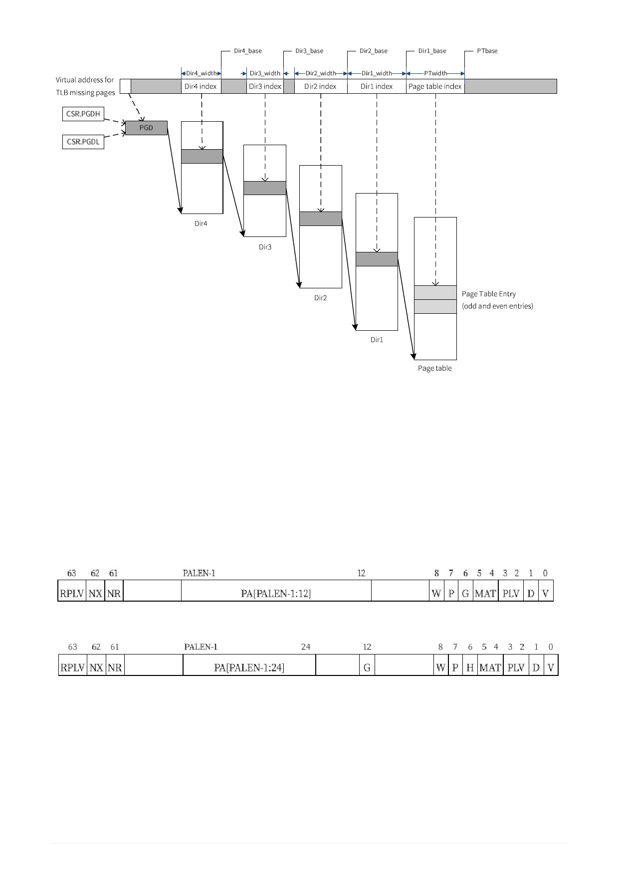
Figure 7. Multi-level page table structure supported by page walking
The base address of the top-level directory (global directory) of the traversed page table called PGD is
determined by the (PALEN-1) bit of the queried virtual address. When this bit is 0, the PGD comes from
CSR.PGDL; when this bit is 1, the PGD comes from CSR.PGDH. This means that the entire page table
structure is (PALEN-1) bits.
The specifications of each level of directory entries and page table entries are configured by the system
software in CSR.PWCL and CSR.PWCH.
Whether the LDDIR and LDPTE instructions are used to implement software page walking or hardware page
walking, the system software needs to define the page table entries in the following format.
Figure 8. Table entry format for common pages
Figure 9. Table entry format for huge pages
In the above definition of the page table entry format, the main differences between the page table entry of
a huge page and the page table entry of a common page are:
1.
Bit 6 of the directory entry is the huge page table entry flag bit, and 1 indicates that the directory entry
actually stores the page table entry of a huge page at this time;
2.
The G bit of the common page table entry is in bit 6, while the G bit of the huge page table entry is in bit
12.
112
Bits not defined in either of these formats are automatically ignored by the LDDIR and LDPTE instructions
or hardware page walking.
The P field defined in the above page table entry format represents whether the physical page exists, and
the W field represents whether the page is writable. This information is not filled in the TLB table entry, but
is used during the page walking.
Due to the double-page memory structure of the TLB table entries, for the huge page table entries (which
has only one), the hardware page table refill or the software LDPTE instruction will automatically split the
two page table entries in half according to the information of the huge page table entries and then fill in the
TLB. For example, if the standard page size is 16KB, the size of the first-level huge page size is usually
32MB. After the LDPTE rj, 0 and LDPTE rj, 1 instructions are executed during page walking, The TLB
will be filled with two page table entries (page size is 16MB) without special software intervention.
Because the address mapping is in direct address translation mode during TLB Refill exception (TLBR), the
addresses configured in the PGD and in the directory entries of the page table in memory must be physical
addresses.
113
Chapter 6. Exceptions and interrupts
6.1. Interrupts
6.1.1. Interrupt Types
Interrupts in LoongArch take the form of line-based interrupts. Each processor core can record 13 line-
based interrupts: one Inter-Processor Interrupt (IPI), one Timer Interrupt (TI), one Performance Monitor
Counter Overflow Interrupt (PMCOV), eight HardWare Interrupts (HWI0-HWI7), and two SoftWare Interrupts
(SWI0-SWI1). All line-based interrupts are level-triggered and are high level triggered.
The interrupt source for inter-processor interrupts comes from an interrupt controller outside the core,
which is recorded by the processor core in the CSR.ESTA.IS[12] bit.
The interrupt source for the timer interrupt is from the constant frequency timer in the core. This interrupt is
triggered when the constant frequency timer counts down to zero. The timer interrupt is recorded by the
processor core in the CSR.ESTA.IS[11] bit. Clearing the timer interrupt is accomplished by the software
via writing 1 to CSR.TICLR.TI.
The interrupt source for the performance monitor counter overflow interrupt comes from the performance
monitor counter in the core. This interrupt is triggered when the [63] bit of the performance counter of any
enabled interrupt is 1. The performance monitor counter overflow interrupt is recorded by the processor
core in the CSR.ESTA.IS[10] bit. To clear a performance monitor counter overflow interrupt, set the
performance monitor counter of the interrupt that is triggered to 0 at the [63] bit, or disable the interrupt
for that performance monitor counter.
The interrupt source for hardware interrupts comes from outside the processor core, and its direct source
is usually an interrupt controller outside the core. 8 hardware interrupts (HWI[7:0]) are recorded by the
processor core in the CSR.ESTA.IS[9:2] bits .
The source of the software interrupt comes from the internal core of the processor, and the software writes
1 to CSR.ESTA.IS[1:0] to set up the software interrupt and 0 to clear it.
The index of the location of the interrupt recorded by the CSR.ESTA.IS field is also called the Interrupt
Number (Int Number). Int number for SWI0 is equal to 0, int number for SWI1 is equal to 1, … , int number of
IPI is equal to 12.
6.1.2. Interrupt Priority
The response to multiple interrupts at the same time is arbitrated by a fixed priority. The higher the int
number, the higher the priority. Therefore, IPI has the highest priority, TI the second highest, … , SWI0 has
the lowest priority.
6.1.3. Interrupt Entry
Interrupts are treated as an exception once they are marked to the instruction by the processor, so the
calculation of interrupt entries follows the rules for calculating general exception entries. See Exception
Entry for the rules of calculating the general exception entries. The exception number for an interrupt is its
own int number plus 64. The exception number for interrupt SWI0 is 64, the exception number for interrupt
SWI1 is 65, … , and so on.
6.1.4. Process of Processor Responding to Interrupts
The interrupt signal from each interrupt source is recorded by the processor in the CSR.ESTA.IS field. The
114
value of this field and the value of the local interrupt enable field configured by software in the
CSR.ECFG.LIE field perform the bitwise AND operation to obtain a 13-bit interrupt vector (int_vec).
When CSR.CRMD.IE=1 and int_vec is not all 0 values, the processor considers that there is an interrupt
that needs to be responded to. So the processor picks an instruction from the executed instruction stream
and marks it with a special kind of exception — interrupt exception.
The subsequent process of the processor is the same as that of the general exception, see the description
in General Hardware Exception Handling of General Exceptions.
6.2. Exceptions
6.2.1. Exception Entry
The entry for the TLB refill exception comes from CSR.TLBRENTRY.
The entry for the machine error exception comes from CSR.MERRENTRY.
Exceptions other than the above two exceptions are called general exceptions, and their entries are
calculated by address|offset. Here | is a bitwise OR operation.
All general exception entries have the same base address from CSR.EENTRY.
The offset of the general exception entry is determined by both the mode of the interrupt offset and the
exception number (ecode), which is equal to 2(CSR.ERG.V+2)×(ecode+64). See the ecode column in Table of
exception encoding for general exceptions except interrupts; the ecode for interrupts is its int number plus
64.
When CSR.ECFG.VS=0, all general exceptions have the same entry, and the software needs to determine
the specific exception type by Ecode and IS fields in CSR.ESTA. When CSR.ECFG.VS!=0, different
interrupt sources have different exception entries and the software does not need to confirm the exception
type by CSR.ESTA.
Since the exception entry is an offset on the base address calculated by bitwise OR operation, when
CSR.ECFG.VS!=0, during assigning the exception entry base address, the software needs to ensure that
all possible offsets do not exceed the bound alignment space corresponding to the low bit of the entry base
address.
6.2.2. Exception Priority
The exception priority follows two basic principles: first, the interrupt priority is higher than the exception;
second, for the exception, the highest priority is detected in the fetching stage, followed by the priority
detected in the decoding stage, and the priority detected in the execution stage.
For exceptions detected in the fetching stage: the highest priority is given to the fetch operation watchpoint
exception, the second highest priority is given to the fetch operation address error exception, the second
highest priority is given to TLB-related exceptions, and the lowest priority is given to the machine error
exception.
The exceptions that can be detected in the decoding stage are mutually exclusive, so there is no need to
consider the priority between them.
Only memory access instructions may trigger multiple exceptions at the same time during the execution
stage, with the following priorities in descending order: Address aLignment fault Exception (ALE) caused by
unaligned addresses for memory access instructions requesting alignment addresses > ADdress error
Exception (ADE) > Bound Check Exception (BCE)[1] > TLB-related exceptions[2] > Address aLignment fault
Exception (ALE) caused by addresses that span two pages of different Cache attributes for memory access
115
instructions allowing non-alignment addresses.
6.2.3. General Hardware Exception Handling of General Exceptions
There may be some differences in the handling of different general exceptions by the processor, and the
general hardware exception handling of general exceptions is described here.
When a general exception is triggered, the processor does the following:
•
Store PLV and IE in CSR.CRMD to PPLV and PIE in CSR.PRMD, then set PLV in CSR.CRMD to 0 and IE
to 0;
•
For implementations that support the Watch function, also store WE in CSR.CRMD to PWE in CSR.PRMD
and then set WE in CSR.CRMD to 0;
•
Record PC that triggered the exception by CSR.ERA;
• Jump to the exception entry to fetch instructions.
When the software executes the ERTN instruction returning from general exceptions, the processor does
the following:
•
Restore PPLV and PIE in CSR.PRMD to PLV and IE in CSR.CRMD;
•
For implementations that support the Watch function, also restore PWE in CSR.PRMD to WE in
CSR.CRMD;
•
Jump to the address recorded by CSR.ERA to fetch instructions.
For the above hardware implementation, the software needs to save PPLV and PIE in CSR.PRMD if the
interrupt needs to be enabled during the exception handling, and restore the saved contents to CSR.PRMD
before the exception returns.
6.2.4. Hardware Exception Handling of TLB Refill Exception
When the TLB refill exception is triggered, the processor does the following:
•
Store PLV and IE in CSR.CRMD to PPLV and PIE in CSR.TLBRPRMD, then set PLV in CSR.CRMD to 0,
IE to 0, DA to 1 and PG to 0.
•
For implementations that support the Watch function, also store WE in CSR.CRMD to PWE in
CSR.TLBRPRMD, and then set WE in CSR.CRMD to 0;
•
Record the
[GRLEN-1:2] bits of the PC that triggered the exception instruction by ERA in
CSR.TLBRERA, and set IsTLBR in CSR.TLBRERA to 1;
•
Record the virtual memory access address that triggered the exception (or PC if triggered by fetching
instructions) by CSR.TLBRBADV and the [PALEN-1:13] bits of address by VPPN in CSR.TLBREHI;
•
Jump to the exception entry configured by CSR.TLBRENTRY to fetch instructions.
When software executes the ERTN instruction to return from TLB refill exception, the processor does the
following:
•
Restore PPLV and PIE in CSR.TLBRPRMD to PLV and IE in CSR.CRMD;
•
For implementations that support the Watch function, restore PWE in CSR.TLBRPRMD to WE in
CSR.CRMD;
116
•
Set DA in CSR.CRMD to 0 and PG to 1;
•
Set IsTLBR in CSR.TLBRERA to 0;
•
Jump to the address recorded by CSR.TLBRERA to fetch instructions.
6.2.5. Hardware Exception Handling of Machine Error Exception
When the machine error exception is triggered, the processor does the following:
•
Store PLV, IE, DA, PG, DATF and DATM in CSR.CRMD to PPLV, PIE, PDA, PPG, PDATF and PDATM in
CSR.MERRCTL, then set PLV in CSR.CRMD to 0, IE to 0, DA to 1, PG to 0, DATF to 0, and DATM to 0;
•
For implementations that support the Watch function, also store WE in CSR.CRMD to PWE in
CSR.MERRCTL, and then set WE in CSR.CRMD to 0;
•
Record PC that triggered the exception instruction by CSR.MERRERA;
•
Set IsMERR in CSR.MERRCTL to 1;
•
Record the specific error message by CSR.ERRINFO and CSR.MERRINFO1;
•
Jump to the exception entry configured by CSR.MERRENTRY to fetch instructions.
When the software executes the ERTN instruction returning from the machine error exception, the
processor does the following:
•
Restore PPLV, PIE, PDA, PPG, PDATF and PDATM in CSR.MERRCTL;
•
For implementations that support the Watch function, also restore PWE in CSR.MERRCTL to WE in
CSR.CRMD;
•
Set the IsMERR in CSR.TLBRERA to 0;
•
Jump to the address recorded by CSR.MERRERA to fetch instructions.
6.3. Reset
A reset will reset all logic in the processor core and place the circuit in a determined state. The definition of
the state of the processor after reset is given here.
The PC after the reset is 0x1C000000. Since the MMU must be in direct address translation mode after the
reset, the physical address of the first instruction fetched after reset is also 0x1000000.
After the reset, the contents of the registers in the determined state are:
•
PLV in CSR.CRMD is 0, IE is 0, DA is 1, PG is 0, DATF is 0, DATM is 0, and WE is 0;
•
FPUen, VPUen, XVPUen and BTUen in CSR.PUCTL are all 0 values;
•
All configurable bits in CSR.MISC are 0;
•
VS and LIE in CSR.ECFG are 0;
•
All bits of IS[1:0] in CSR.ESTA are 0;
•
RDVA in CSR.RVACFG is 0;
•
En in CSR.TCFG is 0;
•
KLO in CSR.LLBCTL is 0;
117
•
IsTLBR in CSR.TLBRERA is 0;
•
IsMERR in CSR.MERRCTL is 0;
•
PLV0-PLV3 in all implemented CSR.DMWs are 0;
•
All configurable bits except EvCode in all implemented CSR.PMCFGs are 0;
•
All configurable bits in all implemented data breakpoint CSRs are 0;
•
All configurable bits in all implemented instruction breakpoint CSRs are 0;
•
DST in CSR.DEBUG is 0.
In addition to what is specified above, the values of all other software-visible registers in the processor are
undefinded after the reset. The software has to set their values before they can be used.
Whether TLB and Cache need to do a hardware reset during the reset is decided by the implementation.
The software responsible for booting determines whether to do a software reset via the processor
configuration information.
1. It is generated only when it is a memory access instruction of bound class.
2. The definition of TLB-related exceptions dictates that only one TLB-related exception will be generated by a single memory access
instruction in any case.
118
Chapter 7. Control and Status Registers
7.1. Overview of Control and Status Registers
Table 14. Overview of Control and Status Registers
Address
Name
CuRrent MoDe information
0x0
CRMD
PRe-exception MoDe information
0x1
PRMD
0x2
Extended component Unit ENable
EUEN
MISCellaneous controller
0x3
MISC
Exception ConFiGuration
0x4
ECFG
0x5
Exception STATus
ESTAT
Exception Return Address
0x6
ERA
BAD virtual Address
0x7
BADV
0x8
BAD Instruction
BADI
Exception ENTRY address
0xC
EENTRY
TLB InDeX
0x10
TLBIDX
0x11
TLB Entry HIgh-order bits
TLBEHI
TLB Entry LOw-order bits 0
0x12
TLBELO0
TLB Entry LOw-order bits 1
0x13
TLBELO1
0x18
Address Space IDentifier
ASID
Page Global Directory base address for Lower half address
0x19
PGDL
space
Page Global Directory base address for Higher half address
0x1A
PGDH
space
Page Global Directory base address
0x1B
PGD
Page Walk Controller for Lower half address space
0x1C
PWCL
0x1D
Page Walk Controller for Higher half address space
PWCH
STLB Page Size
0x1E
STLBPS
Reduced Virtual Address ConFiGuration
0x1F
RVACFG
0x20
CPU IDentity
CPUID
Privileged Resource ConFiGuration 1
0x21
PRCFG1
Privileged Resource ConFiGuration 2
0x22
PRCFG2
0x23
Privileged Resource ConFiGuration 3
PRCFG3
Data SAVA register
0x30+n (0 ≤ n ≤
SAVEn
15)
0x40
Timer IDentity
TID
Timer ConFiGuration
0x41
TCFG
119
Address
Name
0x42
Timer VALue
TVAL
CouNTer Compensation
0x43
CNTC
Timer Interrupt CLeaRing
0x44
TICLR
0x60
LLBit ConTroLler
LLBCTL
IMPlementation-specific ConTroLler 1
0x80
IMPCTL1
IMPlementation-specific ConTroLler 2
0x81
IMPCTL2
0x88
TLB Refill exception ENTRY address
TLBRENTRY
TLB Refill exception BAD Virtual address
0x89
TLBRBADV
TLB Refill Exception Return Address
0x8A
TLBRERA
0x8B
TLB Refill exception data SAVE register
TLBRSAVE
TLB Refill exception Entry LOw-order bits 0
0x8C
TLBRELO0
TLB Refill exception Entry LOw-order bits 1
0x8D
TLBRELO1
0x8E
TLB Refill exception Entry HIgh-order bits
TLBREHI
TLB Refill exception PRe-exception MoDe information
0x8F
TLBRPRMD
Machine ERRor ConTroLler
0x90
MERRCTL
0x91
Machine ERRor INFOrmation 1
MERRINFO1
Machine ERRor INFOrmation 2
0x92
MERRINFO2
Machine ERRor exception ENTRY address
0x93
MERRENTRY
0x94
Machine ERRor Exception Return Address
MERRERA
Machine ERRor exception data SAVE register
0x95
MERRSAVE
Cache TAGs
0x98
CTAG
0x180+n (0 ≤ n
Direct Mapping configuration Window n
DMWn
≤ 3)
Performance Monitor ConFiGuration n
0x200+2n (0 ≤ n
PMCFGn
≤ 31)
Performance Monitor overall CouNTer n
0x201+2n (0 ≤ n
PMCNTn
≤ 31)
0x300
Memory load/store WatchPoint overall Controller
MWPC
Memory load/store WatchPoint overall Status
0x301
MWPS
Memory load/store WatchPoint n ConFiGuration 1
0x310+8n (0 ≤ n
MWPnCFG1
≤ 7)
Memory load/store WatchPoint n ConFiGuration 2
0x311+8n (0 ≤ n
MWPnCFG2
≤ 7)
0x312+8n (0 ≤ n
Memory load/store WatchPoint n ConFiGuration 3
MWPnCFG3
≤ 7)
120
Address
Name
0x313+8n (0 ≤ n
Memory load/store WatchPoint n ConFiGuration 4
MWPnCFG4
≤ 7)
Fetch WatchPoint overall Controller
0x380
FWPC
0x381
Fetch WatchPoint overall Status
FWPS
Fetch WatchPoint n ConFiGuration 1
0x390+8n (0 ≤ n
FWPnCFG1
≤ 7)
0x391+8n (0 ≤ n
Fetch WatchPoint n ConFiGuration 2
FWPnCFG2
≤ 7)
Fetch WatchPoint n ConFiGuration 3
0x392+8n (0 ≤ n
FWPnCFG3
≤ 7)
Fetch WatchPoint n ConFiGuration 4
0x393+8n (0 ≤ n
FWPnCFG4
≤ 7)
0x500
DeBuG register
DBG
Debug Exception Return Address
0x501
DERA
Debug data SAVE register
0x502
DSAVE
7.2. Characteristics of Accessing Control and Status
Registers
7.2.1. Attributes of Reading and Writing
The definition of the “read/write” attribute for each field is described later in this manual in the control and
status register field definition. The “read/write” attributes are defined primarily from the perspective of
software and are divided into four types:
• RW - readable and writable. Software can write any value, except for illegal values that are explicitly
stated in the definition and lead to uncertainty in the processor’s execution. Normally, software writes
to these fields before it reads them, and what is read should be the value written. However, when the
accessed field can be updated by hardware, or when an interrupt occurs between the two instructions
executing the read and write operation, it is possible that the read value is not consistent with the
written value.
• R - read-only. Software writes to these fields will not update their contents, and will have no side
effects.
•
R0 - always return 0 if read these fields. But at the same time software must ensure that either it avoids
updating these fields by setting the CSR write mask bit, or it must write 0 when updating these fields.
This requirement is to ensure software backward compatibility. For hardware implementations, fields
marked with this attribute will prohibit software writing.
•
W1 - write 1 is valid. Software writes 0 to these fields will not clear them to 0 and will have no side
effects. Also, the read values of these fields have no real meaning and software should ignore these
values.
7.2.2. Length of Control and Status Registers in LA32 and LA64
The length of all status control registers is either fixed 32 bits, or it depends on whether the implementation
is LA32 or LA64. For the first type of registers, when they are accessed by CSR instructions in LA64, retrun
values of reading these registers are symbolic expansion to 64 bits, and bits higher than 32 bits of values of
121
writing to them are automatically ignored by hardware. For the second type, the definitions will clearly
indicate the difference between LA32 and LA64.
7.2.3. Access Effects of Undefined and Unimplemented Control and Status Registers
When software uses CSR instructions to access CSR objects that are not defined in the architecture
specification or that are implementable entries defined in the architecture specification but not
implemented by the specific hardware, the return value of reading can be any value, but the write operation
will not change the software-visible processor state.
Although software writes to these undefined or unimplemented status control registers do not change the
software-visible processor state, software should not write to these registers if it wants to ensure backward
compatibility.
7.3. Conflicts Caused by Control and Status Registers
Conflicts caused by the control and status register are maintained by the hardware, and the software does
not need to add barrier-type instructions for avoiding conflict.
7.4. Basic Control and Status Registers
7.4.1. Current Mode Information (CRMD)
The information in this register is used to determine the the processor core’s privilege level, global interrupt
enable bit, watchpoint enable bit, and address translation mode at that time.
Table 15. Definition of current mode information register
Bits
Name
Read/Write
Description
RW
1:0
PLV
Current privilege level. The legal value range is 0 to 3, where 0 is
the highest privilege level and 3 is the lowest privilege level.
When an exception is triggered, the hardware sets the value of
this field to 0 to ensure that it is at the highest privilege level after
being caught.
When the ERTN instruction is executed to return from the
exception handler, if CSR.MERRCTL.IsMERR=1, the hardware
restores the value of the PPLV field of CSR.MERRCTL to here;
otherwise, if CSR.TLBRERA.IsTLBR=1, the hardware restores
the value of the PPLV field of CSR.TLBRPRMD to here; otherwise,
the hardware restores the value of the PPLV field of
CSR.TLBRPRMD to here;
otherwise, the hardware restores the value of the PPLV field of
CSR.TLBRPRMD to here. Hardware restores the value of the PPLV
field of CSR.PRMD to here.
122
Bits
Name
Read/Write
Description
2
IE
RW
Current global interrupt enable bit, which is active high.
When an exception is triggered, the hardware sets the value of
this field to 0, to ensure that the interrupt is masked when caught.
This field needs to be explicitly set to 1 when the exception
handler decides to re-open the interrupt response.
When the ERTN instruction is executed to return from the
exception handler, if CSR.MERRCTL.IsMERR=1, the hardware
restores the value of the PIE field of CSR.MERRCTL to this field;
Otherwise, if CSR.TLBRERA.IsTLBR=1, the hardware restores
the value of the PIE field of CSR.TLBRPRMD here;
Otherwise, the hardware restores the value of the PIE field of
CSR.PRMD to here.
3
DA
RW
Direct address translation mode enable bit, which is active high.
The hardware sets this field to 1 when a TLB refill exception or a
machine error exception is triggered.
If CSR.MERRCTL.IsMERR=1, the hardware restores the value of
the PDA field of CSR.MERRCTL when the ERTN instruction is
executed and returns from the exception handler;
otherwise, if CSR.TLBRERA.IsTLBR=1, the hardware sets this
field to 0.
The legal combination of DA and PG bits is 0, 1 or 1, 0. The result
is uncertain when the software is configured for other
combinations.
4
PG
RW
Mapped address translation mode enable bit, which is active high.
The hardware sets this field to 0 when a TLB refill exception or a
machine error exception is triggered.
When the ERTN instruction is executed to return from an
exception handler,
if CSR.MERRCTL.IsMERR=1, the hardware restores the value of
the PPG field of CSR.MERRCTL to this;
otherwise, if CSR.TLBRERA.IsTLBR=1, the hardware sets this
field to 1.
The legal combination of PG and DA bits is 0, 1 or 1, 0. The result
is uncertain when the software is configured for other
combinations.
123
Bits
Name
Read/Write
Description
6:5
DATF
RW
The type of memory access for fetch operations when in direct
address translation mode.
The hardware sets this field to 0 when a machine error exception
is triggered.
When the execution of the ERTN instruction returns from the
exception handler and CSR.MERRCTL.IsMERR=1, the hardware
restores the value of the PDATF field of CSR.MERRCTL to here.
In the case of using software to handle TLB refill, when the
software sets PG to 1, it needs to set the DATF field to 0b01 at
the same time, which is the consistent cacheable type.
RW
The type of memory access for load and store operations when in
8:7
DATM
direct address translation mode.
The hardware sets this field to 0 when a machine error exception
is triggered.
When the execution of the ERTN instruction returns from the
exception handler and CSR.MERRCTL.IsMERR=1, the hardware
restores the value of the PDATM field of CSR.MERRCTL to here.
In the case of using software to handle TLB refill, when the
software sets PG to 1, it needs to set DATM to 0b01 at the same
time, i.e., consistent cacheable type.
9
WE
RW
Instruction and data watchpoints enable bit, which is active high.
The hardware sets the value of this field to 0 when an exception is
triggered.
When the ERTN instruction is executed to return from the
exception handler.
If CSR.MERRCTL.IsMERR=1, the hardware restores the value of
the PWE field of CSR.MERRCTL to here;
otherwise, if CSR.TLBRERA.IsTLBR=1, the hardware restores
the value of the PWE field of CSR.TLBRPRMD to here;
Otherwise, the hardware restores the value of the PWE field of
CSR.PRMD here.
31:10
0
R0
Reserved field. Return 0 if read this field and the software does
not allow to change its value.
7.4.2. Pre-exception Mode Information (PRMD)
When an exception is triggered, if the exception type is not TLB refill exception and machine error
exception, the hardware will save the processor core’s privilege level, global interrupt enable bit and
watchpoint enable bit at that time to the pre-exception mode information register for restoring the
processor core to the context when the exception returns.
124
Table 16. Definition of pre-exception mode information register
Bits
Name
Read/Write
Description
1:0
PPLV
RW
When an exception is triggered, the hardware records the old
value of the PLV field in CSR.CRMD in this field if the exception
type is not a TLB refill exception and a machine error exception.
When the exception being processed is neither a TLB refill
exception (CSR.TLBRERA.IsTLBR=0) nor a machine error
exception (CSR.MERRCTL.IsMERR=0), the hardware restores the
value of this field to the PLV field of CSR.CRMD when the ERTN
instruction is executed to return from the exception handler.
RW
When an exception is triggered, the hardware records the old
2
PIE
value of the IE field in CSR.CRMD in this field if the exception type
is not a TLB refill exception and a machine error exception.
When the exception being processed is neither a TLB refill
exception (CSR.TLBRERA.IsTLBR=0) nor a machine error
exception (CSR.MERRCTL.IsMERR=0), the hardware restores the
value of this field to the IE field of CSR.CRMD when the ERTN
instruction is executed to return from the exception handler.
RW
When an exception is triggered, the hardware records the old
3
PWE
value of the WE field in CSR.CRMD in this field if the exception type
is not a TLB refill exception and a machine error exception.
When the exception being processed is neither a TLB refill
exception (CSR.TLBRERA.IsTLBR=0) nor a machine error
exception (CSR.MERRCTL.IsMERR=0), the hardware restores the
value of this field to the WE field of CSR.CRMD when the ERTN
instruction is executed to return from the exception handler.
R0
31:4
0
Reserved field. Return 0 if read this field and the software does
not allow to change its value.
7.4.3. Extended Component Unit Enable (EUEN)
In addition to the base integer instruction set and the privileged instruction set, the base floating-point
instruction set, the binary translation extension instruction set, the 128-bit vector extension instruction set,
and the 256-bit vector extension instruction set each have software-configurable enable bits. When these
enable controls are disabled, execution of the corresponding instruction will trigger the corresponding
instruction unavailable exception. Software uses this mechanism to determine the scope when saving the
context. Hardware implementations can also use the control bits here to implement circuit power control.
Table 17. Definition of extended component unit enable register
Bits
Name
Read/Write
Description
RW
0
FPE
The base floating-point instruction enable bit. When this bit is 0,
execution of the base floating-point instruction as described in
Overview of Floating-Point Instructions will trigger a floating-point
instruction disable exception (FPD).
RW
The 128-bit vector expansion instruction enable bit. When this bit
1
SXE
is 0, execution of the 128-bit vector expansion instruction as
described in Volume 2 will trigger the 128-bit vector expansion
instruction disable exception (SXD).
125
Bits
Name
Read/Write
Description
2
ASXE
RW
The 256-bit vector expansion instruction enables the control bit.
When this bit is 0, execution of the 256-bit vector expansion
instruction as described in Volume 2 will trigger the 256-bit vector
expansion instruction disable exception (ASXD).
RW
Binary translation expansion instruction enable bit. When this bit
3
BTE
is 0, execution of the binary translation expansion instruction
described in Volume 2 will trigger the binary translation expansion
instruction disable exception (BTD).
31:4
0
R0
Reserved field. Return 0 if read this field, and software is not
allowed to change its value.
7.4.4. Miscellaneous Controller (MISC)
This register contains a number of control bits for the operating behavior of the processor core at different
privilege levels, including whether to enable 32-bit address mode, whether to allow partially privileged
instructions at non-privileged levels, whether to enable address non-alignment check, and whether to
enable page table write protection check.
Table 18. Definition of miscellaneous controller register
Bits
Name
Read/Write
Description
0
0
RO
Reserved field. Return 0 if read this field and software is not
allowed to change its value.
RW
Whether to enable 32-bit address mode at the PLV1 privilege
1
VA32L1
level. 0 - disable, 1 - enable. This bit can be read and written only
in LA64, at the LA32 privilege level, this attribute is R0.
RW
Whether to turn on 32-bit address mode at the PLV2 privilege
2
VA32L2
level. 0 - disable, 1 - enable. This bit is read/write only in LA64,
and at the LA32 privilege level, this attribute is R0.
RW
Whether to enable 32-bit address mode at the PLV3 privilege
3
VA32L3
level. 0 - disable, 1 - enable. This bit is read/write only in LA64,
and at the LA32 privilege level, this attribute is R0.
4
0
R0
Reserved field. Return 0 if read this field and software is not
allowed to change its value.
RW
Whether to disable RDTIME-like instructions at the PLV1 privilege
5
DRDTL1
level. When this bit is 1, execution of an RDTIME-like instruction at
the PLV1 privilege level will trigger an instruction privilege level
error exception (IPE).
6
DRDTL2
RW
Whether to disable RDTIME-like instructions at the PLV2 privilege
level. When this bit is 1, execution of RDTIME-like instructions at
PLV2 privilege level will trigger instruction privilege level error
exception (IPE).
RW
Whether to disable RDTIME class instructions at the PLV3
7
DRDTL3
privilege level. When this bit is 1, execution of RDTIME-like
instructions at the PLV3 privilege level will trigger an instruction
privilege level error exception (IPE).
8
0
R0
Reserved field. Return 0 if read this field and software is not
allowed to change its value.
126