Intel 64 and IA-32 Architectures. Software Developer’s Manual (2026) - page 48
PROTECTED-MODE MEMORY MANAGEMENT
offset against the segment limit. For example, when the granularity flag is set, a limit of 0 results in
valid offsets from 0 to 4095.
L (64-bit code segment) flag
In IA-32e mode, bit 21 of the second doubleword of the segment descriptor indicates whether a
code segment contains native 64-bit code. A value of 1 indicates instructions in this code segment
are executed in 64-bit mode. A value of 0 indicates the instructions in this code segment are
executed in compatibility mode. If the L-bit is set, then the D-bit must be cleared. Bit 21 is not used
outside IA-32e mode (or for data segments). Because an attempt to activate IA-32e mode will fault
if the current CS has the L-bit set (see Section 12.8.5), software operating outside IA-32e mode
should avoid loading CS from a descriptor that sets the L-bit.
Available and reserved bits
Bit 20 of the second doubleword of the segment descriptor is available for use by system software.
3.4.5.1
Code- and Data-Segment Descriptor Types
When the S (descriptor type) flag in a segment descriptor is set, the descriptor is for either a code or a data
segment. The highest order bit of the type field (bit 11 of the second double word of the segment descriptor) then
determines whether the descriptor is for a data segment (clear) or a code segment (set).
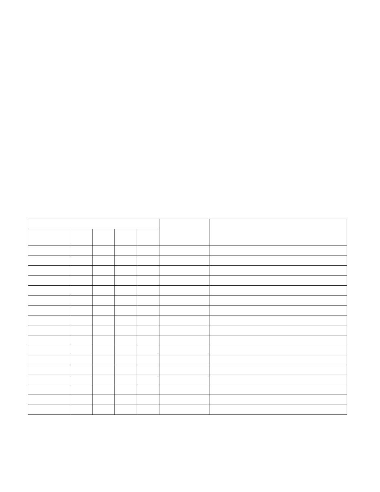
For data segments, the three low-order bits of the type field (bits 8, 9, and 10) are interpreted as accessed (A),
write-enable (W), and expansion-direction (E). See Table 3-1 for a description of the encoding of the bits in the
type field for code and data segments. Data segments can be read-only or read/write segments, depending on the
setting of the write-enable bit.
Table 3-1. Code- and Data-Segment Types
Type Field
Descriptor
Description
Type
Decimal
11
10
9
8
E
W
A
0
0
0
0
0
Data
Read-Only
1
0
0
0
1
Data
Read-Only, accessed
2
0
0
1
0
Data
Read/Write
3
0
0
1
1
Data
Read/Write, accessed
4
0
1
0
0
Data
Read-Only, expand-down
5
0
1
0
1
Data
Read-Only, expand-down, accessed
6
0
1
1
0
Data
Read/Write, expand-down
7
0
1
1
1
Data
Read/Write, expand-down, accessed
C
R
A
8
1
0
0
0
Code
Execute-Only
9
1
0
0
1
Code
Execute-Only, accessed
10
1
0
1
0
Code
Execute/Read
11
1
0
1
1
Code
Execute/Read, accessed
12
1
1
0
0
Code
Execute-Only, conforming
13
1
1
0
1
Code
Execute-Only, conforming, accessed
14
1
1
1
0
Code
Execute/Read, conforming
15
1
1
1
1
Code
Execute/Read, conforming, accessed
Stack segments are data segments which must be read/write segments. Loading the SS register with a segment
selector for a nonwritable data segment generates a general-protection exception (#GP). If the size of a stack
segment needs to be changed dynamically, the stack segment can be an expand-down data segment (expansion-
3-12
Vol. 3A
PROTECTED-MODE MEMORY MANAGEMENT
direction flag set). Here, dynamically changing the segment limit causes stack space to be added to the bottom of
the stack. If the size of a stack segment is intended to remain static, the stack segment may be either an expand-
up or expand-down type.
The accessed bit indicates whether the segment has been accessed since the last time the operating-system or
executive cleared the bit. The processor sets this bit whenever it loads a segment selector for the segment into a
segment register, assuming that the type of memory that contains the segment descriptor supports processor
writes. The bit remains set until explicitly cleared. This bit can be used both for virtual memory management and
for debugging.
For code segments, the three low-order bits of the type field are interpreted as accessed (A), read enable (R), and
conforming (C). Code segments can be execute-only or execute/read, depending on the setting of the read-enable
bit. An execute/read segment might be used when constants or other static data have been placed with instruction
code in a ROM. Here, data can be read from the code segment either by using an instruction with a CS override
prefix or by loading a segment selector for the code segment in a data-segment register (the DS, ES, FS, or GS
registers). In protected mode, code segments are not writable.
Code segments can be either conforming or nonconforming. A transfer of execution into a more-privileged
conforming segment allows execution to continue at the current privilege level. A transfer into a nonconforming
segment at a different privilege level results in a general-protection exception (#GP), unless a call gate or task gate
is used (see Section 6.8.1, “Direct Calls or Jumps to Code Segments,” for more information on conforming and
nonconforming code segments). System utilities that do not access protected facilities and handlers for some types
of exceptions (such as, divide error or overflow) may be loaded in conforming code segments. Utilities that need to
be protected from less privileged programs and procedures should be placed in nonconforming code segments.
NOTE
Execution cannot be transferred by a call or a jump to a less-privileged (numerically higher
privilege level) code segment, regardless of whether the target segment is a conforming or
nonconforming code segment. Attempting such an execution transfer will result in a general-
protection exception.
All data segments are nonconforming, meaning that they cannot be accessed by less privileged programs or proce-
dures (code executing at numerically higher privilege levels). Unlike code segments, however, data segments can
be accessed by more privileged programs or procedures (code executing at numerically lower privilege levels)
without using a special access gate.
If the segment descriptors in the GDT or an LDT are placed in ROM, the processor can enter an indefinite loop if
software or the processor attempts to update (write to) the ROM-based segment descriptors. To prevent this
problem, set the accessed bits for all segment descriptors placed in a ROM. Also, remove operating-system or
executive code that attempts to modify segment descriptors located in ROM.
3.5
SYSTEM DESCRIPTOR TYPES
When the S (descriptor type) flag in a segment descriptor is clear, the descriptor type is a system descriptor. The
processor recognizes the following types of system descriptors:
• Local descriptor-table (LDT) segment descriptor.
• Task-state segment (TSS) descriptor.
• Call-gate descriptor.
• Interrupt-gate descriptor.
• Trap-gate descriptor.
• Task-gate descriptor.
These descriptor types fall into two categories: system-segment descriptors and gate descriptors. System-
segment descriptors point to system segments (LDT and TSS segments). Gate descriptors are in themselves
“gates,” which hold pointers to procedure entry points in code segments (call, interrupt, and trap gates) or which
hold segment selectors for TSS’s (task gates).
Vol. 3A
3-13
PROTECTED-MODE MEMORY MANAGEMENT
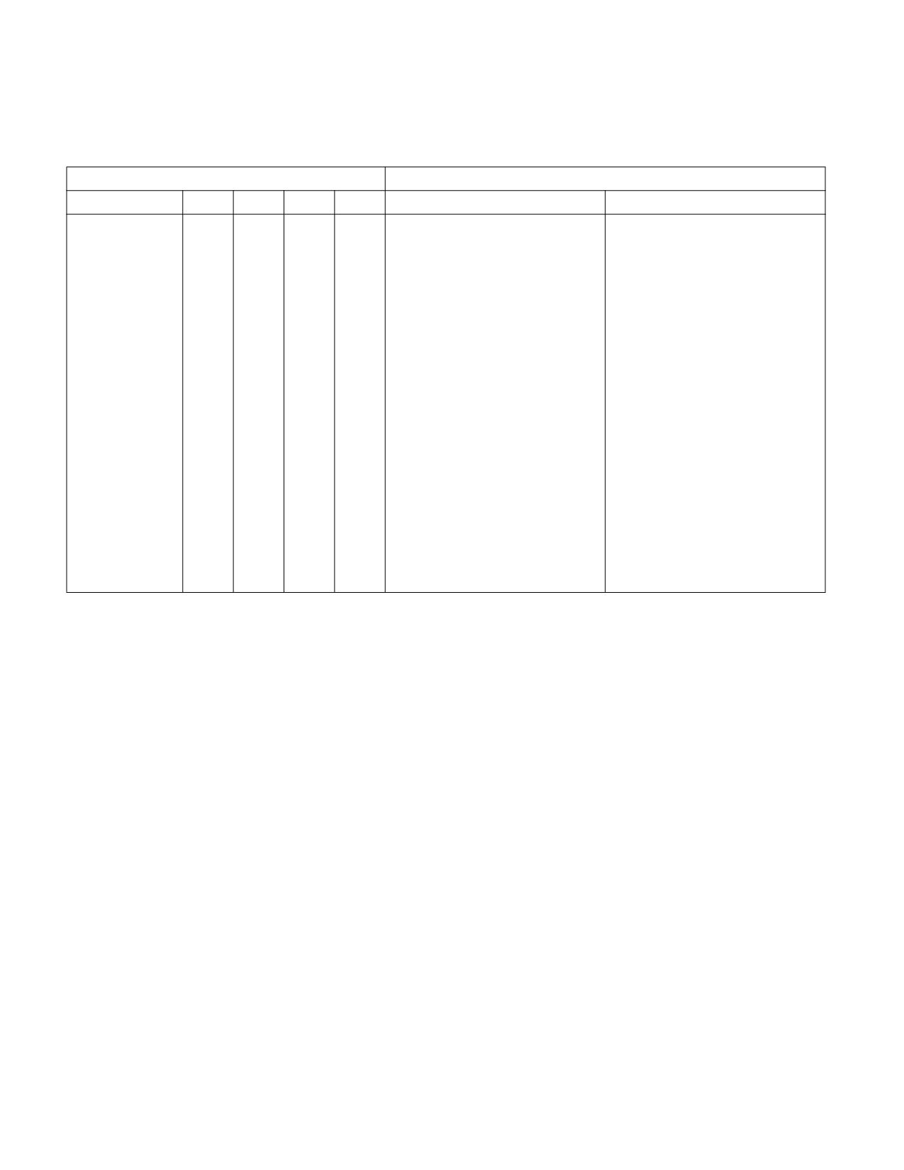
Table 3-2 shows the encoding of the type field for system-segment descriptors and gate descriptors. Note that
system descriptors in IA-32e mode are 16 bytes instead of 8 bytes.
Table 3-2. System-Segment and Gate-Descriptor Types
Type Field
Description
Decimal
11
10
9
8
32-Bit Mode
IA-32e Mode
0
0
0
0
0
Reserved
Reserved
1
0
0
0
1
16-bit TSS (Available)
Reserved
2
0
0
1
0
LDT
LDT
3
0
0
1
1
16-bit TSS (Busy)
Reserved
4
0
1
0
0
16-bit Call Gate
Reserved
5
0
1
0
1
Task Gate
Reserved
6
0
1
1
0
16-bit Interrupt Gate
Reserved
7
0
1
1
1
16-bit Trap Gate
Reserved
8
1
0
0
0
Reserved
Reserved
9
1
0
0
1
32-bit TSS (Available)
64-bit TSS (Available)
10
1
0
1
0
Reserved
Reserved
11
1
0
1
1
32-bit TSS (Busy)
64-bit TSS (Busy)
12
1
1
0
0
32-bit Call Gate
64-bit Call Gate
13
1
1
0
1
Reserved
Reserved
14
1
1
1
0
32-bit Interrupt Gate
64-bit Interrupt Gate
15
1
1
1
1
32-bit Trap Gate
64-bit Trap Gate
See also: Section 3.5.1, “Segment Descriptor Tables,” and Section 10.2.2, “TSS Descriptor,” (for more information
on the system-segment descriptors); see Section 6.8.3, “Call Gates,” Section 7.11, “IDT Descriptors,” and Section
10.2.5, “Task-Gate Descriptor,” (for more information on the gate descriptors).
3.5.1
Segment Descriptor Tables
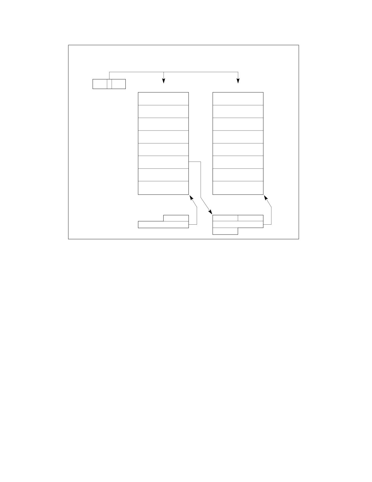
A segment descriptor table is an array of segment descriptors (see Figure 3-10). A descriptor table is variable in
length and can contain up to 8192 (213) 8-byte descriptors. There are two kinds of descriptor tables:
• The global descriptor table (GDT).
• The local descriptor tables (LDT).
3-14
Vol. 3A
PROTECTED-MODE MEMORY MANAGEMENT
Global
Local
Descriptor
Descriptor
Table (GDT)
Table (LDT)
T
I
TI = 0
TI = 1
Segment
Selector
56
56
48
48
40
40
32
32
24
24
16
16
8
8
First Descriptor in
GDT is Not Used
0
0
GDTR Register
LDTR Register
Limit
Limit
Base Address
Base Address
Seg. Sel.
Figure 3-10. Global and Local Descriptor Tables
Each system must have one GDT defined, which may be used for all programs and tasks in the system. Optionally,
one or more LDTs can be defined. For example, an LDT can be defined for each separate task being run, or some
or all tasks can share the same LDT.
The GDT is not a segment itself; instead, it is a data structure in linear address space. The base linear address and
limit of the GDT must be loaded into the GDTR register (see Section 2.4, “Memory-Management Registers”). The
base address of the GDT should be aligned on an eight-byte boundary to yield the best processor performance. The
limit value for the GDT is expressed in bytes. As with segments, the limit value is added to the base address to get
the address of the last valid byte. A limit value of 0 results in exactly one valid byte. Because segment descriptors
are always 8 bytes long, the GDT limit should always be one less than an integral multiple of eight (that is, 8N - 1).
The first descriptor in the GDT is not used by the processor. A segment selector to this “null descriptor” does not
generate an exception when loaded into a data-segment register (DS, ES, FS, or GS), but it always generates a
general-protection exception (#GP) when an attempt is made to access memory using the descriptor. By initializing
the segment registers with this segment selector, accidental reference to unused segment registers can be guar-
anteed to generate an exception.
The LDT is located in a system segment of the LDT type. The GDT must contain a segment descriptor for the LDT
segment. If the system supports multiple LDTs, each must have a separate segment selector and segment
descriptor in the GDT. The segment descriptor for an LDT can be located anywhere in the GDT. See Section 3.5,
“System Descriptor Types,” for information on the LDT segment-descriptor type.
An LDT is accessed with its segment selector. To eliminate address translations when accessing the LDT, the
segment selector, base linear address, limit, and access rights of the LDT are stored in the LDTR register (see
Section 2.4, “Memory-Management Registers”).
When the GDTR register is stored (using the SGDT instruction), a 48-bit “pseudo-descriptor” is stored in memory
(see top diagram in Figure 3-11). To avoid alignment check faults in user mode (privilege level 3), the pseudo-
descriptor should be located at an odd word address (that is, address MOD 4 is equal to 2). This causes the
Vol. 3A
3-15

PROTECTED-MODE MEMORY MANAGEMENT
processor to store an aligned word, followed by an aligned doubleword. User-mode programs normally do not store
pseudo-descriptors, but the possibility of generating an alignment check fault can be avoided by aligning pseudo-
descriptors in this way. The same alignment should be used when storing the IDTR register using the SIDT instruc-
tion. When storing the LDTR or task register (using the SLDT or STR instruction, respectively), the pseudo-
descriptor should be located at a doubleword address (that is, address MOD 4 is equal to 0).
47
16 15
0
32-bit Base Address
Limit
79
16 15
0
64-bit Base Address
Limit
Figure 3-11. Pseudo-Descriptor Formats
3.5.2
Segment Descriptor Tables in IA-32e Mode
In IA-32e mode, a segment descriptor table can contain up to 8192 (213) 8-byte descriptors. An entry in the
segment descriptor table can be 8 bytes. System descriptors are expanded to 16 bytes (occupying the space of two
entries).
GDTR and LDTR registers are expanded to hold 64-bit base address. The corresponding pseudo-descriptor is 80
bits. (see the bottom diagram in Figure 3-11).
The following system descriptors expand to 16 bytes:
- Call gate descriptors (see Section 6.8.3.1, “IA-32e Mode Call Gates”).
- IDT gate descriptors (see Section 7.14.1, “64-Bit Mode IDT”).
- LDT and TSS descriptors (see Section 10.2.3, “TSS Descriptor in 64-bit mode”).
3-16
Vol. 3A
CHAPTER 4
LINEAR-ADDRESS PRE-PROCESSING
As described in Chapter 3, “Protected-Mode Memory Management‚” software accesses to memory typically use
logical addresses. The processor uses segmentation, as detailed in Section 3.4, to generate linear addresses from
logical addresses. Linear addresses are then translated to physical addresses using paging, as described in Chapter
5, “Paging.”
In IA-32e mode (if IA32_EFER.LMA = 1), linear addresses may undergo some pre-processing before being trans-
lated through paging.1 Some of this pre-processing is done only if enabled by software, but some occurs uncondi-
tionally. Specifically, linear addresses are subject to pre-processing in IA-32e mode as follows:
1. Linear-address-space separation (LASS). This is a feature that, when enabled by software, may limit the
linear addresses that are accessible by software, generating faults for accesses out of range.
2. Linear-address masking (LAM). This is a feature that, when enabled by software, masks certain linear-
address bits.
3. Canonicality checking. As will be detailed in Chapter 5, paging does not translate all 64 bits of a linear
address. Each linear address must be canonical, meaning that the untranslated bits have a fixed value.
Memory accesses using a non-canonical address generate faults.
Both LASS and canonicality checking can generate faults. For any specific memory access, the two features
generate the same fault. For that reason, the relative order of that checking is not defined and cannot be deter-
mined by software.
4.1
ENABLING AND ENUMERATION
Software enables LASS by setting CR4.LASS[bit 27]. Enabling of LAM is based on three different bits:
CR3.LAM_U48[bit 62], CR3.LAM_U57[bit 61], and CR4.LAM_SUP[bit 28]. The use of these bits is explained in
Section 4.4. Canonicality checking is not enabled by software and is always performed in 64-bit mode.
The processor enumerates support for LASS with CPUID.07H.01H:EAX.LASS[6]. If this bit is enumerated as 1, soft-
ware can set CR4.LASS.
The processor enumerates support for LAM with CPUID.07H.01H:EAX.LAM[26]. If this bit is enumerated as 1, soft-
ware can set CR3.LAM_U48, CR3.LAM_U57, and CR4.LAM_SUP.
4.2
MODE-BASED ACCESSES AND LINEAR-ADDRESS-SPACE PARTITIONING
Every access to a linear address is either a supervisor-mode access or a user-mode access. For all instruction
fetches and most data accesses, this distinction is determined by the current privilege level (CPL): accesses made
while CPL < 3 are supervisor-mode accesses, while accesses made while CPL = 3 are user-mode accesses.
Some operations implicitly access system data structures with linear addresses; the resulting accesses to those
data structures are supervisor-mode accesses regardless of CPL. Such accesses include the following: accesses to
the global descriptor table (GDT) or local descriptor table (LDT) to load a segment descriptor; accesses to the inter-
rupt descriptor table (IDT) when delivering an interrupt or exception; accesses to the task-state segment (TSS) as
part of a task switch or change of CPL; and accesses to a user posted-interrupt descriptor (UPID) during user-inter-
rupt notification processing. Such accesses are called implicit supervisor-mode accesses regardless of CPL.
Other accesses made while CPL < 3 are called explicit supervisor-mode accesses.2
1. The presentation in this chapter focuses on 64-bit addresses. 32-bit and 16-bit addresses can also be used in IA-32e mode. For the
purposes of this chapter, the upper bits of such addresses (32 bits and 48 bits, respectively) are treated as if they were all zero.
2. The WRUSS instruction is an exception; although it can be executed only if CPL = 0, the processor treats its shadow-stack accesses
as user-mode accesses.
Vol. 3A
4-1
LINEAR-ADDRESS PRE-PROCESSING
Some 64-bit operating systems partition the 64-bit linear-address space into a supervisor portion and a user
portion. Specifically, the upper half of the linear-address space (comprising addresses in which bit 63 is 1) is used
for supervisor instructions and data, while the lower half (addresses in which bit 63 is 0) is for user instructions and
data.
The LASS and LAM features are designed for operating systems that establish such linear-address-space parti-
tioning. However, the features are defined and may be used even if such partitioning is not in effect.
4.3
LINEAR-ADDRESS-SPACE SEPARATION (LASS)
The access rights determined by paging (see Section 5.6) are based on whether a linear address is a supervisor-
mode address or a user-mode address. Paging provides protection by preventing user-mode accesses to super-
visor-mode addresses; in addition, there are paging features that can prevent supervisor-mode accesses to user-
mode addresses.
These paging-based protections prevent malicious software from directly reading or writing memory inappropri-
ately. However, they require the processor to traverse a hierarchy of paging structures in memory. Unprivileged
software may be able to use the timing information resulting from this traversal to determine details about the
paging structures, the layout of supervisor memory, or its use by supervisor software.
Linear-address-space separation (LASS) is an independent mechanism that can enforce mode-based protection
without traversing the paging structures. Because LASS provides this protection as part of linear-address pre-
processing, unprivileged software is denied paging-based timing information.
An operating system can use LASS to provide protections corresponding to the mode-based paging protections if it
has established the linear-address-space partitioning outlined in Section 4.2.
4.3.1
Enumeration and Enabling
The processor enumerates support for LASS with CPUID.07H.01H:EAX.LASS[6].
Software enables LASS by setting CR4.LASS[bit 27]. CR4.LASS can be set to 1 if CPUID.07H.01H:EAX.LASS[6] is
enumerated as 1.
The operation of LASS is also affected by the paging-mode bit CR4.SMAP[bit 21], which enables supervisor-access
prevention. LASS enforces the equivalent of supervisor-mode execution prevention regardless of the setting of
CR4.SMEP[bit 17]. See Section 4.3.2 for details.
4.3.2
Operation of Linear-Address-Space Separation (LASS)
This section describes the operation of linear-address-space separation (LASS). This operation applies only in
IA-32e mode (if IA32_EFER.LMA = 1) and only if CR4.LASS = 1.
As indicated earlier, LASS enforces protections similar to those enforced by paging. Violations of these protections
are called LASS violations.
LASS violations typically result in faults. In most cases, an access causing a LASS violation results in a general
protection exception (#GP); for stack accesses (those due to stack-oriented instructions, as well as accesses that
implicitly or explicitly use the SS segment register), a stack fault (#SS) is generated. In either case, a null error
code is produced.
Some accesses are not subject to faults due to LASS violations. These include prefetches (e.g., those resulting from
execution of one of the PREFETCHh instructions), executions of the CLDEMOTE instruction, and accesses resulting
from the speculative fetch or execution of an instruction. Such an access may cause a LASS violation; if it does, the
access is not performed but no fault occurs.
The remainder of this section describes how LASS applies to different types of accesses to linear addresses. The
items below discuss specific LASS violations based on bit 63 of a linear address. For a linear address with only 32
bits (or 16 bits), the processor treats bit 63 as if it were 0; this includes accesses in compatibility mode.
• A user-mode data access causes a LASS violation if it would access a linear address of which bit 63 is 1.
4-2
Vol. 3A
LINEAR-ADDRESS PRE-PROCESSING
• A supervisor-mode data access causes a LASS violation if it would access a linear address of which bit 63 is 0,
supervisor-mode access protection is enabled (by setting CR4.SMAP), and either RFLAGS.AC = 0 or the access
is an implicit supervisor-mode access.
• A user-mode instruction fetch causes a LASS violation if it would fetch an instruction using a linear address of
which bit 63 is 1.
• A supervisor-mode instruction fetch causes a LASS violation if it would accesses a linear address of which bit 63
is 0. (Unlike paging, this behavior of LASS applies regardless of the setting of CR4.SMEP.)
LASS for instruction fetches applies when the linear address in RIP is used to load an instruction from memory.
Unlike canonicality checking (see Section 4.5.2), LASS does not apply to branch instructions that load RIP. A
branch instruction can load RIP with an address that would violate LASS. Only when the address is used to fetch an
instruction will a LASS violation occur, generating a #GP. (The return instruction pointer of the #GP handler is the
address that incurred the LASS violation.)
4.4
LINEAR-ADDRESS MASKING
This section describes linear-address masking (LAM). LAM modifies linear addresses before they are subject to
canonicality checking as described in Section 4.5. Doing so allows untranslated linear-address bits to contain arbi-
trary values.
In IA-32e mode, linear address have 64 bits and are translated either with 4-level paging, which translates the low
48 bits of each linear address, or with 5-level paging, which translates 57 bits. The upper linear-address bits are
reserved by canonicality checking (see Section 4.5).
Software usages that associate metadata with a pointer might benefit from being able to place metadata in the
upper (untranslated) bits of the pointer itself. However, the canonicality enforcement mentioned earlier implies
that software would have to mask the metadata bits in a pointer (making it canonical) before using it as a linear
address to access memory. LAM allows software to use pointers with metadata without having to mask the meta-
data bits. With LAM enabled, the processor masks the metadata bits in a pointer before using it as a linear address
to access memory.
LAM applies only to 64-bit linear addresses used for data accesses. It does not apply to addresses used for instruc-
tion fetches or to those being loaded into the RIP register (e.g., as targets of jump and call instructions).
4.4.1
Enumeration, Enabling, and Configuration
The processor enumerates support for LAM with CPUID.07H.01H:EAX.LAM[26].
Enabling and configuration of LAM is controlled by the following control-register bits: CR3.LAM_U48[bit 62],
CR3.LAM_U57[bit 61], and CR4.LAM_SUP[bit 28]. The use of these control bits is explained below.
LAM supports configurations that differ regarding which linear-address bits are masked and can be used for meta-
data. With LAM48, linear-address bits 62:48 are masked (resulting in a LAM width of 15); with LAM57, linear-
address bits 62:57 are masked (a LAM width of 6).
Like LASS, LAM was designed for operating systems that establish the linear-address-space partitioning outlined in
Section 4.2: linear addresses that clear bit 63 are used for user memory, while those that set bit 63 are for super-
visor memory. For LAM, the identification of an address as user or supervisor is based solely on the value of bit 63
and does not depend on the CPL.
LAM and the LAM width can be configured independently for user and supervisor addresses (as identified in the
previous paragraph, using bit 63). CR3.LAM_U48 and CR3.LAM_U57 enable and configure LAM for user addresses:
• If CR3.LAM_U48 = CR3.LAM_U57 = 0, LAM is not enabled for user addresses.
• If CR3.LAM_U48 = 1 and CR3.LAM_U57 = 0, LAM48 is enabled for user addresses (a LAM width of 15).
• If CR3.LAM_U57 = 1, LAM57 is enabled for user addresses (a LAM width of 6; CR3.LAM_U48 is ignored in this
case).
CR4.LAM_SUP enables and configures LAM for supervisor addresses:
• If CR4.LAM_SUP = 0, LAM is not enabled for supervisor addresses.
Vol. 3A
4-3
LINEAR-ADDRESS PRE-PROCESSING
• If CR4.LAM_SUP = 1, LAM is enabled for supervisor addresses with a width determined by the paging mode
(see Section 5.1.1):
- If 4-level paging is enabled, LAM48 is enabled for supervisor addresses (a LAM width of 15).
- If 5-level paging is enabled, LAM57 is enabled for supervisor addresses (a LAM width of 6).
4.4.2
Treatment of Data Accesses with LAM Active
When LAM is active, linear addresses used to access data are masked before they are subject to the canonicality
checking identified in Section 4.5. Specifically, LAM modifies a linear address by extending the value of one address
bit (depending on the LAM width) over others:
• When LAM48 is enabled (see Section 4.4.1), the processor modifies each linear address to replace each of
bits 62:48 with the value of bit 47.
• When LAM57 is enabled, each of bits 62:57 is replaced by the value of bit 56 (bits 56:48 are not modified).
4.4.3
Paging Interactions
As explained in Section 4.4.2, LAM masks certain bits in a linear address before that address is translated by
paging.
In most cases, the address bits in the masked positions are not used by address translation. However, if 5-level
paging is active and LAM48 is enabled for user pointers, bit 47 of a user pointer is extended over bits 62:48 to form
a linear address, and bits 56:48 are used by 5-level paging.
Page faults report the faulting linear address in CR2. Because LAM masking applies before paging, the faulting
linear address recorded in CR2 reflects the result of that masking and does not contain any masked metadata.
The INVLPG, INVPCID, and INVVPID instructions can be used to invalidate any translation lookaside buffer (TLB)
entries for specified linear addresses. LAM does not apply to those addresses, although those addresses are subject
to canonicality checking (see Section 4.5.4).
4.5
CANONICALITY CHECKING
Memory accesses in IA-32e mode can use 64-bit linear addresses. As detailed in Section 5.5.4, 4-level paging
translates the low 48 bits of each linear address, while 5-level paging translates the low 57 bits. The remaining
upper bits (bits 63:48 with 4-level paging; bits 63:57 with 5-level paging) are not translated.
IA-32e mode accounts for the fact that address bits are not translated (and thus should be reserved) with the
concept of canonicality. In general, a linear address is canonical if the untranslated bits are a sign-extension of
the most significant translated bit. More specifically, there are two types of canonicality:
• A linear address is paging canonical if it is canonical for the current paging mode: a linear address is canonical
for 4-level paging (48-bit canonical) if bits 63:47 of the address are identical; it is canonical for 5-level paging
(57-bit canonical) if bits 63:56 are identical.
• A linear address is CPU canonical if it is canonical relative to the widest linear address supported by the
processor: 48-bit canonical if the processor supports only 4-level paging and 57-bit canonical if the processor
supports 5-level paging.
Unlike LASS and LAM, there is no control to enable canonicality checking. It always applies (as described in this
section) when 64-bit linear addresses are used.
Section 4.5.1 and Section 4.5.2 explain canonicality checking for accesses to memory using linear addresses and
for loads of the instruction pointer, respectively. Section 4.5.3 details how canonicality checking applies to certain
system registers that contain linear addresses. Section 4.5.4 explains the role of canonicality checking by instruc-
tions that invalidate TLB entries.
4-4
Vol. 3A
LINEAR-ADDRESS PRE-PROCESSING
NOTE
Section 4.5.2 and Section 4.5.3 discuss the canonicality checking performed by the WRMSR
instruction. The WRMSRLIST and WRMSRNS instructions perform the same canonicality checking in
corresponding situations. (Similarly, the characterization of RDMSR in Section 4.5.3 applies also to
RDMSRLIST.)
4.5.1
Memory Accesses
An access to memory using a linear address is allowed only if the address is paging canonical; if it is not, a canon-
icality violation occurs. In most cases, an access causing a canonicality violation results in a general protection
exception (#GP); for stack accesses (those due to stack-oriented instructions, as well as accesses that implicitly or
explicitly use the SS segment register), a stack fault (#SS) is generated. In either case, a null error code is
produced.
When LAM is enabled, canonicality checking is performed after masking of the linear address. This implies that the
requirements of canonicality on an original (unmasked) linear address used to access data are effectively relaxed
when LAM is enabled:
• With LAM48, bit 63 and bit 47 of the original linear address must be identical.
• With LAM57 and 4-level paging, bit 63 and bits 56:47 of the original linear address must be identical.
• With LAM57 and 5-level paging, bit 63 and bit 56 of the original linear address must be identical.
While LAM applies only to data accesses, canonicality checking applies both data accesses and instruction fetches.
4.5.2
Loads of the Instruction Pointer (RIP)
In 64-bit mode, the RIP register contains the linear address of the instruction pointer. Operations that load RIP
(including both instructions such as JMP as well as control transfers through the IDT) check first whether the value
to be loaded is paging canonical. If it is not, the operation does not modify RIP and instead causes a #GP. (This #GP
is delivered as a fault, meaning that the return instruction pointer of the fault handler is the address of the faulting
instruction and not the non-canonical address whose load was attempted.)
This treatment applies to the SYSRET and SYSEXIT instructions, which load RIP from RCX and RDX, respectively.
The SYSCALL and SYSENTER instructions load RIP from the IA32_LSTAR and IA32_SYSENTER_EIP MSRs, respec-
tively. On processors that support only 4-level paging, these instructions do not check explicitly that the values
being loaded are paging canonical. This is because the WRMSR instruction ensures that these MSRs necessarily
contain values that are CPU canonical, which is the same as being paging canonical on processors that support only
4-level paging. On processors that support 5-level paging, the checking by WRMSR is relaxed to ensure only 57-bit
canonicality. (See Section 4.5.3 for the treatment of WRMSR.) On such processors, an execution of SYSCALL or
SYSENTER with 4-level paging checks that the value being loaded into RIP is 48-bit canonical (paging canonical).
4.5.3
System Registers Containing Linear Addresses
In addition to RIP, the CPU maintains numerous other registers that hold linear addresses:
• GDTR and IDTR (in their base-address portions).
• LDTR, TR, FS, and GS (in the base-address portions of their hidden descriptor caches).
• Control register CR2, which holds the linear address causing a page fault.
• The debug-address registers (DR0 through DR3), which hold the linear addresses of breakpoints.
• The following MSRs: IA32_BNDCFGS, IA32_DS_AREA, IA32_FS_BASE, IA32_GS_BASE,
IA32_INTERRUPT_SSP_TABLE_ADDR, IA32_KERNEL_GS_BASE, IA32_LSTAR, IA32_PL0_SSP, IA32_PL1_SSP,
IA32_PL2_SSP, IA32_PL3_SSP, IA32_RTIT_ADDR0_A, IA32_RTIT_ADDR0_B, IA32_RTIT_ADDR1_A,
IA32_RTIT_ADDR1_B, IA32_RTIT_ADDR2_A, IA32_RTIT_ADDR2_B, IA32_RTIT_ADDR3_A,
IA32_RTIT_ADDR3_B, IA32_S_CET, IA32_SYSENTER_EIP, IA32_SYSENTER_ESP, IA32_UINTR_HANDLER,
IA32_UINTR_PD, IA32_UINTR_STACKADJUST, IA32_U_CET, and IA32_UINTR_TT.
• The x87 FPU instruction pointer (FIP).
Vol. 3A
4-5
LINEAR-ADDRESS PRE-PROCESSING
• The user-mode configuration register BNDCFGU, used by Intel® MPX.
With a few exceptions, the processor ensures that the addresses in these registers are always canonical in the
following ways:
•
Some instructions fault on attempts to load a linear-address register with a non-canonical address:
- An execution of the LGDT or LIDT instruction causes a general-protection exception (#GP) if the base
address specified in the instruction’s memory operand is not canonical.
- An execution of the LLDT or LTR instruction causes a #GP if the base address to be loaded from the GDT is
not canonical.
- An execution of WRFSBASE or WRGSBASE causes a #GP if it would load the base address of either FS or GS
with a non-canonical address.
- An execution of WRMSR causes a #GP if it would load any of the following MSRs with a non-canonical
address: IA32_BNDCFGS, IA32_DS_AREA, IA32_FS_BASE, IA32_GS_BASE,
IA32_INTERRUPT_SSP_TABLE_ADDR, IA32_KERNEL_GS_BASE, IA32_LSTAR, IA32_PL0_SSP,
IA32_PL1_SSP, IA32_PL2_SSP, IA32_PL3_SSP, IA32_RTIT_ADDR0_A, IA32_RTIT_ADDR0_B,
IA32_RTIT_ADDR1_A, IA32_RTIT_ADDR1_B, IA32_RTIT_ADDR2_A, IA32_RTIT_ADDR2_B,
IA32_RTIT_ADDR3_A, IA32_RTIT_ADDR3_B, IA32_S_CET, IA32_SYSENTER_EIP, IA32_SYSENTER_ESP,
IA32_UINTR_HANDLER, IA32_UINTR_PD, IA32_UINTR_STACKADJUST, IA32_U_CET, and
IA32_UINTR_TT.1
- An execution of XRSTORS causes a #GP if it would load any of the following MSRs with a non-canonical
address: IA32_PL0_SSP, IA32_PL1_SSP, IA32_PL2_SSP, IA32_PL3_SSP, IA32_RTIT_ADDR0_A,
IA32_RTIT_ADDR0_B, IA32_RTIT_ADDR1_A, IA32_RTIT_ADDR1_B, IA32_RTIT_ADDR2_A,
IA32_RTIT_ADDR2_B, IA32_RTIT_ADDR3_A, IA32_RTIT_ADDR3_B, IA32_U_CET,
IA32_UINTR_HANDLER, IA32_UINTR_PD, IA32_UINTR_STACKADJUST, or IA32_UINTR_TT.
With a small number of exceptions, this enforcement checks for CPU canonicality and is thus independent of the
current paging mode. Thus, a processor that supports 5-level paging will allow the instructions mentioned
above to load these registers with addresses that are 57-bit canonical but not 48-bit canonical, even if 4-level
paging is active. (As a result, instructions that store these values - SGDT, SIDT, SLDT, STR, RDFSBASE,
RDGSBASE, RDMSR, XSAVE, XSAVEC, XSAVEOPT, and XSAVES - may save addresses that are 57-bit canonical
but not 48-bit canonical, even if 4-level paging is active.)
The WRFSBASE and WRGSBASE instructions, which load the base address of FS and GS, respectively, operate
differently. An execution of either of these instructions causes a #GP if it would load a base address with an
address that is not paging canonical. Thus, if 4-level paging is active, these instructions do not allow loading of
addresses that are 57-bit canonical but not 48-bit canonical.
•
The FXRSTOR, XRSTOR, and XRSTORS instructions ignore attempts to load some of these registers with non-
canonical addresses:
- Loads of FIP ignore any bits in the memory image beyond the enumerated maximum linear-address width.
The processor sign-extends the most significant bit (e.g., bit 56 on processors that support 5-level paging)
to ensure that FIP is always CPU canonical.
- Loads of BNDCFGU (by XRSTOR or XRSTORS) ignore any bits in the memory image beyond the enumerated
maximum linear-address width. The processor sign-extends the most significant bit to ensure that
BNDCFGU is always CPU canonical.
•
Every non-control x87 instruction loads FIP. The value loaded is always paging canonical.
•
CR2 can be loaded with the MOV to CR instruction. The instruction allows that register to be loaded with a non-
canonical address. The MOV from CR instruction will return for CR2 the value last loaded into that register by a
page fault or with the MOV to CR instruction, even if (for the latter case) the address is not canonical. Page
faults load CR2 only with linear addresses that are paging canonical.
•
DR0 through DR3 can be loaded with the MOV to DR instruction. The instruction allows those registers to be
loaded with non-canonical addresses. The MOV from DR instruction will return for a debug register the value
1.
Such canonicality checking may apply also when the WRMSR instruction is used to load some non-architec-
tural MSRs (not listed here) that hold a linear address.
4-6
Vol. 3A
LINEAR-ADDRESS PRE-PROCESSING
last loaded into that register with the MOV to DR instruction, even if the address is not canonical. Breakpoint
address matching is supported only for linear addresses that are paging canonical.
4.5.4
TLB-Invalidation Instructions
The Intel 64 architecture includes three instructions that may invalidate TLB entries for the linear address of an
instruction operand: INVLPG, INVPCID, and INVVPID. The following items describe how they are affected by
canonicality.
• The INVLPG instruction takes a memory operand. It invalidates any TLB entries that the logical processor is
caching for the linear address of that operand for the current linear address space. The instruction does not
fault if that address is not paging canonical. However, no invalidation is performed because the processor does
not cache TLB entries for addresses that are not paging canonical.
• The INVPCID instruction takes a register operand (INVPCID type) and a memory operand (INVPCID
descriptor). If the INVPCID type is 0, the instruction invalidates any TLB entries that the logical processor is
caching for the linear address and PCID specified in the INVPCID descriptor. If the linear address is not CPU
canonical, the instruction causes a #GP. If the processor supports 5-level paging, the instruction will not cause
such a #GP for an address that is 57-bit canonical, regardless of paging mode, even if 4-level paging is active
and the address is not 48-bit canonical.
• The INVVPID instruction takes a register operand (INVVPID type) and a memory operand (INVVPID
descriptor). If the INVPCID type is 0, the instruction invalidates any TLB entries that the logical processor is
caching for the linear address and VPID specified in the INVVPID descriptor. If the linear address is not CPU
canonical, the instruction fails.1 If the processor supports 5-level paging, the instruction will not fail for an
address that is 57-bit canonical, regardless of paging mode, even if 4-level paging is active and the address is
not 48-bit canonical.
LAM does not apply to the linear addresses that these instructions use to invalidate TLB entries.
1. INVVPID is a VMX instruction. In response to certain conditions, execution of a VMX instruction may fail, meaning that it does not
complete its normal operation. When a VMX instruction fails, control passes to the next instruction (rather than to a fault handler)
and a flag is set to report the failure.
Vol. 3A
4-7
LINEAR-ADDRESS PRE-PROCESSING
4-8
Vol. 3A
CHAPTER 5
PAGING
Chapter 3 explains how segmentation converts logical addresses to linear addresses. Paging (or linear-address
translation) is the process of translating linear addresses so that they can be used to access memory or I/O
devices. Paging translates each linear address to a physical address and determines, for each translation, what
accesses to the linear address are allowed (the address’s access rights) and the type of caching used for such
accesses (the address’s memory type).
Intel-64 processors support four different paging modes. These modes are identified and defined in Section 5.1.
Section 5.2 gives an overview of the translation mechanism that is used in all modes. Section 5.3, Section 5.4, and
Section 5.5 discuss the four paging modes in detail.
Section 5.6 details how paging determines and uses access rights. Section 5.7 discusses exceptions that may be
generated by paging (page-fault exceptions). Section 5.8 considers data which the processor writes in response to
linear-address accesses (accessed and dirty flags).
Section 5.9 describes how paging determines the memory types used for accesses to linear addresses. Section
5.10 provides details of how a processor may cache information about linear-address translation. Section 5.11
outlines interactions between paging and certain VMX features. Section 5.12 gives an overview of how paging can
be used to implement virtual memory.
5.1
PAGING MODES AND CONTROL BITS
Paging behavior is controlled by the following control bits:
• The WP and PG flags in control register CR0 (bit 16 and bit 31, respectively).
• The PSE, PAE, PGE, LA57, PCIDE, SMEP, SMAP, PKE, CET, and PKS flags in control register CR4 (bit 4, bit 5,
bit 7, bit 12, bit 17, bit 20, bit 21, bit 22, bit 23, and bit 24, respectively).
• The LME and NXE flags in the IA32_EFER MSR (bit 8 and bit 11, respectively).
• The AC flag in the EFLAGS register (bit 18).
• The “enable HLAT” VM-execution control (tertiary processor-based VM-execution control bit 1; see Section
27.6.2, “Processor-Based VM-Execution Controls,” in the Intel® 64 and IA-32 Architectures Software
Developer’s Manual, Volume 3C).
Software enables paging by using the MOV to CR0 instruction to set CR0.PG. Before doing so, software should
ensure control register CR3 contains the physical address of the first paging structure that the processor will use
for linear-address translation (see Section 5.2) and that structure is initialized as desired. See Table 5-3, Table 5-7,
and Table 5-12 for the use of CR3 in the different paging modes.
Section 5.1.1 describes how the values of CR0.PG, CR4.PAE, CR4.LA57, and IA32_EFER.LME determine whether
paging is enabled and, if so, which of four paging modes is in use. Section 5.1.2 explains how to manage these bits
to establish or make changes in paging modes. Section 5.1.3 discusses how CR0.WP, CR4.PSE, CR4.PGE,
CR4.PCIDE, CR4.SMEP, CR4.SMAP, CR4.PKE, CR4.CET, CR4.PKS, and IA32_EFER.NXE modify the operation of the
different paging modes.
5.1.1
Four Paging Modes
If CR0.PG = 0, paging is not used. The logical processor treats all linear addresses as if they were physical
addresses. CR4.PAE, CR4.LA57, and IA32_EFER.LME are ignored by the processor, as are CR0.WP, CR4.PSE,
CR4.PGE, CR4.SMEP, CR4.SMAP, and IA32_EFER.NXE. (CR4.CET is also ignored insofar as it affects linear-address
access rights.)
Paging is enabled if CR0.PG = 1. Paging can be enabled only if protection is enabled (CR0.PE = 1). If paging is
enabled, one of four paging modes is used. The values of CR4.PAE, CR4.LA57, and IA32_EFER.LME determine
which paging mode is used:
Vol. 3A
5-1

PAGING
• If CR4.PAE = 0, 32-bit paging is used. 32-bit paging is detailed in Section 5.3. 32-bit paging uses CR0.WP,
CR4.PSE, CR4.PGE, CR4.SMEP, CR4.SMAP, and CR4.CET as described in Section 5.1.3 and Section 5.6.
• If CR4.PAE = 1 and IA32_EFER.LME = 0, PAE paging is used. PAE paging is detailed in Section 5.4. PAE paging
uses CR0.WP, CR4.PGE, CR4.SMEP, CR4.SMAP, CR4.CET, and IA32_EFER.NXE as described in Section 5.1.3 and
Section 5.6.
• If CR4.PAE = 1, IA32_EFER.LME = 1, and CR4.LA57 = 0, 4-level paging1 is used.2 4-level paging is detailed
in Section 5.5 (along with 5-level paging). 4-level paging uses CR0.WP, CR4.PGE, CR4.PCIDE, CR4.SMEP,
CR4.SMAP, CR4.PKE, CR4.CET, CR4.PKS, and IA32_EFER.NXE as described in Section 5.1.3 and Section 5.6.
• If CR4.PAE = 1, IA32_EFER.LME = 1, and CR4.LA57 = 1, 5-level paging is used. 5-level paging is detailed in
Section 5.5 (along with 4-level paging). 5-level paging uses CR0.WP, CR4.PGE, CR4.PCIDE, CR4.SMEP,
CR4.SMAP, CR4.PKE, CR4.CET, CR4.PKS, and IA32_EFER.NXE as described in Section 5.1.3 and Section 5.6.
NOTE
32-bit paging and PAE paging can be used only in legacy protected mode (IA32_EFER.LME = 0). In
contrast, 4-level paging and 5-level paging can be used only IA-32e mode (IA32_EFER.LME = 1).
The four paging modes differ with regard to the following details:
• Linear-address width. The size of the linear addresses that can be translated.
• Physical-address width. The size of the physical addresses produced by paging.
• Page size. The granularity at which linear addresses are translated. Linear addresses on the same page are
translated to corresponding physical addresses on the same page.
• Support for execute-disable access rights. In some paging modes, software can be prevented from fetching
instructions from pages that are otherwise readable.
• Support for PCIDs. With 4-level paging and 5-level paging, software can enable a facility by which a logical
processor caches information for multiple linear-address spaces. The processor may retain cached information
when software switches between different linear-address spaces.
• Support for protection keys. With 4-level paging and 5-level paging, each linear address is associated with a
protection key. Software can use the protection-key rights registers to disable, for each protection key, how
certain accesses to linear addresses associated with that protection key.
Table 5-1 illustrates the principal differences between the four paging modes.
Table 5-1. Properties of Different Paging Modes
Supports
Lin.-
Phys.-
Supports
Paging
PG in
PAE in
LME in
LA57 in
Page
PCIDs and
Addr.
Addr.
Execute-
Mode
CR0
CR4
IA32_EFER
CR4
Sizes
protection
Width
Width1
Disable?
keys?
None
0
N/A
N/A
N/A
32
32
N/A
No
No
4 KB
32-bit
1
0
02
N/A
32
Up to 403
No
No
4 MB4
4 KB
PAE
1
1
0
N/A
32
Up to 52
Yes5
No
2 MB
4 KB
4-level
1
1
1
0
48
Up to 52
2 MB
Yes5
Yes7
1 GB6
1. Earlier versions of this manual used the term “IA-32e paging” to identify 4-level paging.
2. The LMA flag in the IA32_EFER MSR (bit 10) is a status bit that indicates whether the logical processor is in IA-32e mode (and thus
uses either 4-level paging or 5-level paging). The processor always sets IA32_EFER.LMA to CR0.PG & IA32_EFER.LME. Software can-
not directly modify IA32_EFER.LMA; an execution of WRMSR to the IA32_EFER MSR ignores bit 10 of its source operand.
5-2
Vol. 3A

PAGING
Table 5-1. Properties of Different Paging Modes (Contd.)
Supports
Lin.-
Phys.-
Supports
Paging
PG in
PAE in
LME in
LA57 in
Page
PCIDs and
Addr.
Addr.
Execute-
Mode
CR0
CR4
IA32_EFER
CR4
Sizes
protection
Width
Width1
Disable?
keys?
4 KB
5-level
1
1
1
1
57
Up to 52
2 MB
Yes5
Yes7
1 GB6
NOTES:
1. The physical-address width is always bounded by MAXPHYADDR; see Section 5.1.4.
2. The processor ensures that IA32_EFER.LME must be 0 if CR0.PG = 1 and CR4.PAE = 0.
3. 32-bit paging supports physical-address widths of more than 32 bits only for 4-MByte pages and only if the PSE-36 mechanism is
supported; see Section 5.1.4 and Section 5.3.
4. 32-bit paging uses 4-MByte pages only if CR4.PSE = 1; see Section 5.3.
5. Execute-disable access rights are applied only if IA32_EFER.NXE = 1; see Section 5.6.
6. Processors that support 4-level paging or 5-level paging do not necessarily support 1-GByte pages; see Section 5.1.4.
7. PCIDs are used only if CR4.PCIDE = 1; see Section 5.10.1. Protection keys are used only if certain conditions hold; see Section 5.6.2.
Because 32-bit paging and PAE paging are used only in legacy protected mode and because legacy protected mode
cannot produce linear addresses larger than 32 bits, 32-bit paging and PAE paging translate 32-bit linear
addresses.
4-level paging and 5-level paging are used only in IA-32e mode. IA-32e mode has two sub-modes:
• Compatibility mode. This sub-mode uses only 32-bit linear addresses. In this sub-mode, 4-level paging and 5-
level paging treat bits 63:32 of such an address as all 0. These addresses are subject to linear-address pre-
processing, specifically linear-address-space separation (Section 4.3).
•
64-bit mode. This sub-mode produces 64-bit linear addresses. These addresses are then subject to linear-
address pre-processing (Chapter 4). As part of this, the processor enforces canonicality (Section 4.5),
ensuring that the upper bits of such an address are identical: bits 63:47 for 4-level paging and bits 63:56 for
5-level paging. 4-level paging (respectively, 5-level paging) does not use bits 63:48 (respectively, bits 63:57)
of such addresses.
5.1.2
Paging-Mode Enabling
If CR0.PG = 1, a logical processor is in one of four paging modes, depending on the values of CR4.PAE,
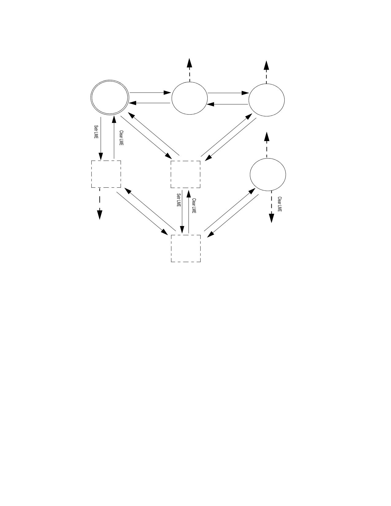
IA32_EFER.LME, and CR4.LA57. Figure 5-1 illustrates how software can enable these modes and make transitions
between them. The following items identify certain limitations and other details:
• IA32_EFER.LME cannot be modified while paging is enabled (CR0.PG = 1). Attempts to do so using WRMSR
cause a general-protection exception (#GP(0)).
• Paging cannot be enabled (by setting CR0.PG to 1) while CR4.PAE = 0 and IA32_EFER.LME = 1. Attempts to do
so using MOV to CR0 cause a general-protection exception (#GP(0)).
• One node in Figure 5-1 is labeled “IA-32e mode.” This node represents either 4-level paging (if CR4.LA57 = 0)
or 5-level paging (if CR4.LA57 = 1). As noted in the following items, software cannot modify CR4.LA57
(effecting transition between 4-level paging and 5-level paging) without first disabling paging.
• CR4.PAE and CR4.LA57 cannot be modified while either 4-level paging or 5-level paging is in use (when
CR0.PG = 1 and IA32_EFER.LME = 1). Attempts to do so using MOV to CR4 cause a general-protection
exception (#GP(0)).
• Regardless of the current paging mode, software can disable paging by clearing CR0.PG with MOV to CR0.1
1. If the logical processor is in 64-bit mode or if CR4.PCIDE = 1, an attempt to clear CR0.PG causes a general-protection exception
(#GP). Software should transition to compatibility mode and clear CR4.PCIDE before attempting to disable paging.
Vol. 3A
5-3
PAGING
#GP
#GP
Set LME
Set LME
No Paging
Set PG
32-bit Paging
Set PAE
PAE Paging
PG = 0
PG = 1
PG = 1
PAE = 0
PAE = 0
PAE = 1
LME = 0
Clear PG
LME = 0
Clear PAE
LME = 0
#GP
Clear PAE
Set PG
Clear PAE
Set PAE
Clear PG
No Paging
No Paging
4-level Paging
PG = 0
PG = 0
PG = 1
PAE = 0
PAE = 1
PAE = 1
LME = 1
LME = 0
LME = 1
Set PG
Set PG
Clear PAE
Clear PG
Set PAE
#GP
#GP
No Paging
PG = 0
PAE = 1
LME = 1
Figure 5-1. Enabling and Changing Paging Modes
•
Software can transition between 32-bit paging and PAE paging by changing the value of CR4.PAE with MOV to
CR4.
•
Software cannot transition directly between 4-level paging (or 5-level paging) and any of other paging mode.
It must first disable paging (by clearing CR0.PG with MOV to CR0), then set CR4.PAE, IA32_EFER.LME, and
CR4.LA57 to the desired values (with MOV to CR4 and WRMSR), and then re-enable paging (by setting CR0.PG
with MOV to CR0). As noted earlier, an attempt to modify CR4.PAE, IA32_EFER.LME, or CR.LA57 while 4-level
paging or 5-level paging is enabled causes a general-protection exception (#GP(0)).
•
VMX transitions allow transitions between paging modes that are not possible using MOV to CR or WRMSR. This
is because VMX transitions can load CR0, CR4, and IA32_EFER in one operation. See Section 5.11.1.
5.1.3
Paging-Mode Modifiers
Details of how each paging mode operates are determined by the following control bits:
• The WP flag in CR0 (bit 16).
• The PSE, PGE, PCIDE, SMEP, SMAP, PKE, CET, and PKS flags in CR4 (bit 4, bit 7, bit 17, bit 20, bit 21, bit 22,
bit 23, and bit 24, respectively).
• The NXE flag in the IA32_EFER MSR (bit 11).
• The “enable HLAT” VM-execution control (tertiary processor-based VM-execution control bit 1).
5-4
Vol. 3A
PAGING
CR0.WP allows pages to be protected from supervisor-mode writes. If CR0.WP = 0, supervisor-mode write
accesses are allowed to linear addresses with read-only access rights; if CR0.WP = 1, they are not. (User-mode
write accesses are never allowed to linear addresses with read-only access rights, regardless of the value of
CR0.WP.) Section 5.6 explains how access rights are determined, including the definition of supervisor-mode and
user-mode accesses.
CR4.PSE enables 4-MByte pages for 32-bit paging. If CR4.PSE = 0, 32-bit paging can use only 4-KByte pages; if
CR4.PSE = 1, 32-bit paging can use both 4-KByte pages and 4-MByte pages. See Section 5.3 for more information.
(PAE paging, 4-level paging, and 5-level paging can use multiple page sizes regardless of the value of CR4.PSE.)
CR4.PGE enables global pages. If CR4.PGE = 0, no translations are shared across address spaces; if CR4.PGE = 1,
specified translations may be shared across address spaces. See Section 5.10.2.4 for more information.
CR4.PCIDE enables process-context identifiers (PCIDs) for 4-level paging and 5-level paging. PCIDs allow a logical
processor to cache information for multiple linear-address spaces. See Section 5.10.1 for more information.
CR4.SMEP allows pages to be protected from supervisor-mode instruction fetches. If CR4.SMEP = 1, software
operating in supervisor mode cannot fetch instructions from linear addresses that are accessible in user mode.
Section 5.6 explains how access rights are determined, including the definition of supervisor-mode accesses and
user-mode accessibility.
CR4.SMAP allows pages to be protected from supervisor-mode data accesses. If CR4.SMAP = 1, software oper-
ating in supervisor mode cannot access data at linear addresses that are accessible in user mode. Software can
override this protection by setting EFLAGS.AC. Section 5.6 explains how access rights are determined, including
the definition of supervisor-mode accesses and user-mode accessibility.
CR4.PKE and CR4.PKS enable specification of access rights based on protection keys. 4-level paging and 5-level
paging associate each linear address with a protection key. When CR4.PKE = 1, the PKRU register specifies, for
each protection key, whether user-mode linear addresses with that protection key can be read or written. When
CR4.PKS = 1, the IA32_PKRS MSR does the same for supervisor-mode linear addresses. See Section 5.6 for more
information.
CR4.CET enables control-flow enforcement technology, including the shadow-stack feature. If CR4.CET = 1,
certain memory accesses are identified as shadow-stack accesses and certain linear addresses translate to
shadow-stack pages. Section 5.6 explains how access rights are determined for these accesses and pages. (The
processor allows CR4.CET to be set only if CR0.WP is also set.)
IA32_EFER.NXE enables execute-disable access rights for PAE paging, 4-level paging, and 5-level paging. If
IA32_EFER.NXE = 1, instruction fetches can be prevented from specified linear addresses (even if data reads from
the addresses are allowed). Section 5.6 explains how access rights are determined. (IA32_EFER.NXE has no effect
with 32-bit paging. Software that wants to use this feature to limit instruction fetches from readable pages must
use PAE paging, 4-level paging, or 5-level paging.)
The “enable HLAT” VM-execution control enables HLAT paging for 4-level paging and 5-level paging. HLAT paging
does not use control register CR3 to identify the address of the first paging str] ] ucture used for linear-address
translation; instead, that structure is located using a field in the virtual-machine control structure (VMCS). In addi-
tion, HLAT paging interprets certain bits in paging-structure entries differently than ordinary paging. See Section
5.5 for details.
5.1.4
Enumeration of Paging Features by CPUID
Software can discover support for different paging features using the CPUID instruction:
• PSE: page-size extensions for 32-bit paging.If CPUID.01H:EDX.PSE[3] = 1, CR4.PSE may be set to 1, enabling
support for 4-MByte pages with 32-bit paging (see Section 5.3).
• PAE: physical-address extension.If CPUID.01H:EDX.PAE[6] = 1, CR4.PAE may be set to 1, enabling PAE paging
(this setting is also required for 4-level paging and 5-level paging).
• PGE: global-page support.If CPUID.01H:EDX.PGE[13] = 1, CR4.PGE may be set to 1, enabling the global-page
feature (see Section 5.10.2.4).
• PAT: page-attribute table.If CPUID.01H:EDX.PAT[16] = 1, the 8-entry page-attribute table (PAT) is supported.
When the PAT is supported, three bits in certain paging-structure entries select a memory type (used to
determine type of caching used) from the PAT (see Section 5.9.2).
Vol. 3A
5-5
PAGING
•
PSE-36: page-size extensions with 40-bit physical-address extension.If CPUID.01H:EDX.PSE_36[17] = 1, the
PSE-36 mechanism is supported, indicating that translations using 4-MByte pages with 32-bit paging may
produce physical addresses with up to 40 bits (see Section 5.3).
•
PCID: process-context identifiers.If CPUID.01H:ECX.PCID[17] = 1, CR4.PCIDE may be set to 1, enabling
process-context identifiers (see Section 5.10.1).
•
SMEP: supervisor-mode execution prevention.If CPUID.07H.00H:EBX.SMEP[7] = 1, CR4.SMEP may be set to
1, enabling supervisor-mode execution prevention (see Section 5.6).
•
SMAP: supervisor-mode access prevention.If CPUID.07H.00H:EBX.SMAP[20] = 1, CR4.SMAP may be set to 1,
enabling supervisor-mode access prevention (see Section 5.6).
•
PKU: protection keys for user-mode pages.If CPUID.07H.00H:ECX.PKU[3] = 1, CR4.PKE may be set to 1,
enabling protection keys for user-mode pages (see Section 5.6).
•
OSPKE: enabling of protection keys for user-mode pages.CPUID.07H.00H:ECX.OSPKE[4] returns the value of
CR4.PKE. Thus, protection keys for user-mode pages are enabled if this flag is 1 (see Section 5.6).
•
CET: control-flow enforcement technology.If CPUID.07H.00H:ECX.CET_SS[7] = 1, CR4.CET may be set to 1,
enabling shadow-stack pages (see Section 5.6).
•
LA57: 57-bit linear addresses and 5-level paging.If CPUID.07H.00H:ECX.LA57[16] = 1, CR4.LA57 may be set
to 1, enabling 5-level paging.
•
PKS: protection keys for supervisor-mode pages.If CPUID.07H.00H:ECX.PKS[31] = 1, CR4.PKS may be set to
1, enabling protection keys for supervisor-mode pages (see Section 5.6).
•
NX: execute disable.If CPUID.80000001H:EDX.EXECUTE_DIS[20] = 1, IA32_EFER.NXE may be set to 1,
allowing software to disable execute access to selected pages (see Section 5.6). (Processors that do not
support CPUID.80000001H do not allow IA32_EFER.NXE to be set to 1.)
•
Page1GB: 1-GByte pages.If CPUID.80000001H:EDX.PAGE_1GB[26] = 1, 1-GByte pages may be supported
with 4-level paging and 5-level paging (see Section 5.5).
•
LM: IA-32e mode support.If CPUID.80000001H:EDX.INTEL64[29] = 1, IA32_EFER.LME may be set to 1,
enabling IA-32e mode (with either 4-level paging or 5-level paging). (Processors that do not support
CPUID.80000001H do not allow IA32_EFER.LME to be set to 1.)
•
CPUID.80000008H:EAX[7:0] reports the physical-address width supported by the processor. (For processors
that do not support CPUID.80000008H, the width is generally 36 if CPUID.01H:EDX.PAE[6] = 1 and 32
otherwise.) This width is at most 52 and is used to determine the value of MAXPHYADDR, which is used by
paging.
If IA32_TME_ACTIVATE[0] = 1 (indicating that TME has been configured), MAXPHYADDR is reduced by the
value of IA32_TME_ACTIVATE[39:36] when a logical processor is outside secure arbitration mode (SEAM; see
Chapter 35); the value is not reduced in SEAM.1
For example, if CPUID.80000008H:EAX[7:0] = 48, IA32_TME_ACTIVATE[39:36] = 4, and TME has been
configured, MAXPHYADDR is 44 outside SEAM (but remains 48 in SEAM).
If the logical processor is in VMX non-root operation and EPT is enabled (see Section 5.11.2), the addresses in
CR3 and in paging-structure entries are treated as guest-physical addresses. The width of these addresses
is limited only by the value enumerated by CPUID.80000008H:EAX[7:0] without any regard to TME or SEAM.
•
CPUID.80000008H:EAX[15:8] reports the linear-address width supported by the processor. Generally, this
value is reported as follows:
- If CPUID.80000001H:EDX.INTEL64[29] = 0, the value is reported as 32.
- If CPUID.80000001H:EDX.INTEL64[29] = 1 and CPUID.07H.00H:ECX.LA57[16] = 0, the value is reported
as 48.
- If CPUID.07H.00H:ECX.LA57[16] = 1, the value is reported as 57.
(Processors that do not support CPUID.80000008H, support a linear-address width of 32.)
1. IA32_TME_ACTIVATE[39:36] is the number of physical-address bits reserved to encode TDX-private key identifiers. This number is
never greater than IA32_TME_ACTIVATE[35:32], which is the number physical-address bits used for key identifiers generally.
5-6
Vol. 3A
PAGING
5.2
HIERARCHICAL PAGING STRUCTURES: AN OVERVIEW
All four paging modes translate linear addresses using hierarchical paging structures. This section provides an
overview of their operation. Section 5.3, Section 5.4, Section 5.5, and Section 5.6 provide details for the four
paging modes.
Every paging structure is 4096 Bytes in size and comprises a number of individual entries. With 32-bit paging,
each entry is 32 bits (4 bytes); there are thus 1024 entries in each structure. With the other paging modes, each
entry is 64 bits (8 bytes); there are thus 512 entries in each structure. (PAE paging includes one exception, a
paging structure that is 32 bytes in size, containing 4 64-bit entries.)
The processor uses the upper portion of a linear address to identify a series of paging-structure entries. The last of
these entries identifies the physical address of the region to which the linear address translates (called the page
frame). The lower portion of the linear address (called the page offset) identifies the specific address within that
region to which the linear address translates.
Each paging-structure entry contains a physical address, which is either the address of another paging structure or
the address of a page frame. In the first case, the entry is said to reference the other paging structure; in the
latter, the entry is said to map a page.
The first paging structure used for any translation is located at the physical address in CR3.1 A linear address is
translated using the following iterative procedure. A portion of the linear address (initially the uppermost bits)
selects an entry in a paging structure (initially the one located using CR3). If that entry references another paging
structure, the process continues with that paging structure and with the portion of the linear address immediately
below that just used. If instead the entry maps a page, the process completes: the physical address in the entry is
that of the page frame and the remaining lower portion of the linear address is the page offset.
The following items give an example for each of the four paging modes (each example locates a 4-KByte page
frame):
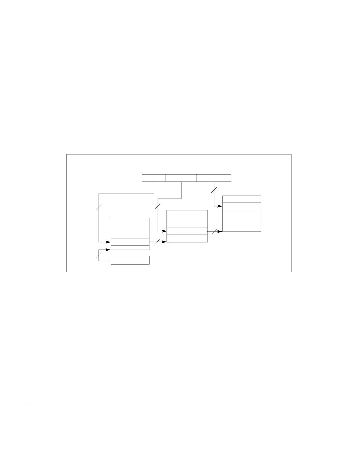
• With 32-bit paging, each paging structure comprises 1024 = 210 entries. For this reason, the translation
process uses 10 bits at a time from a 32-bit linear address. Bits 31:22 identify the first paging-structure entry
and bits 21:12 identify a second. The latter identifies the page frame. Bits 11:0 of the linear address are the
page offset within the 4-KByte page frame. (See Figure 5-2 for an illustration.)
• With PAE paging, the first paging structure comprises only 4 = 22 entries. Translation thus begins by using
bits 31:30 from a 32-bit linear address to identify the first paging-structure entry. Other paging structures
comprise 512 = 29 entries, so the process continues by using 9 bits at a time. Bits 29:21 identify a second
paging-structure entry and bits 20:12 identify a third. This last identifies the page frame. (See Figure 5-5 for
an illustration.)
• With 4-level paging, each paging structure comprises 512 = 29 entries and translation uses 9 bits at a time
from a 48-bit linear address. Bits 47:39 identify the first paging-structure entry, bits 38:30 identify a second,
bits 29:21 a third, and bits 20:12 identify a fourth. Again, the last identifies the page frame. (See Figure 5-8
for an illustration.)
•
5-level paging is similar to 4-level paging except that 5-level paging translates 57-bit linear addresses.
Bits 56:48 identify the first paging-structure entry, while the remaining bits are used as with 4-level paging.
The translation process in each of the examples above completes by identifying a page frame; the page frame is
part of the translation of the original linear address. In some cases, however, the paging structures may be
configured so that the translation process terminates before identifying a page frame. This occurs if the process
encounters a paging-structure entry that is marked “not present” (because its P flag - bit 0 - is clear) or in which
a reserved bit is set. In this case, there is no translation for the linear address; an access to that address causes a
page-fault exception (see Section 5.7).
In the examples above, a paging-structure entry maps a page with a 4-KByte page frame when only 12 bits remain
in the linear address; entries identified earlier always reference other paging structures. That may not apply in
other cases. The following items identify when an entry maps a page and when it references another paging struc-
ture:
• If more than 12 bits remain in the linear address, bit 7 (PS - page size) of the current paging-structure entry
is consulted. If the bit is 0, the entry references another paging structure; if the bit is 1, the entry maps a page.
1. If HLAT paging is in use, a different mechanism is used to identify the first paging structure. See Section 5.5 for more information.
Vol. 3A
5-7
PAGING
• If only 12 bits remain in the linear address, the current paging-structure entry always maps a page (bit 7 is
used for other purposes).
If a paging-structure entry maps a page when more than 12 bits remain in the linear address, the entry identifies
a page frame larger than 4 KBytes. For example, 32-bit paging uses the upper 10 bits of a linear address to locate
the first paging-structure entry; 22 bits remain. If that entry maps a page, the page frame is 222 Bytes = 4 MBytes.
32-bit paging can use 4-MByte pages if CR4.PSE = 1. The other paging modes can use 2-MByte pages (regardless
of the value of CR4.PSE). 4-level paging and 5-level paging can use 1-GByte pages if the processor supports them
(see Section 5.1.4).
Paging structures are given different names based on their uses in the translation process. Table 5-2 gives the
names of the different paging structures. It also provides, for each structure, the source of the physical address
used to locate it (CR3 or a different paging-structure entry); the bits in the linear address used to select an entry
from the structure; and details of whether and how such an entry can map a page.
Table 5-2. Paging Structures in the Different Paging Modes
Physical
Entry
Bits Selecting
Paging Structure
Paging Mode
Address of
Page Mapping
Name
Entry
Structure
32-bit, PAE, 4-level
N/A
PML5 table
PML5E
5-level
CR31
56:48
N/A (PS must be 0)
32-bit, PAE
N/A
PML4 table
PML4E
4-level
CR31
47:39
N/A (PS must be 0)
5-level
PML5E
32-bit
N/A
Page-directory-
PDPTE
PAE
CR3
31:30
N/A (PS must be 0)
pointer table
4-level, 5-level
PML4E
38:30
1-GByte page if PS = 12
32-bit
CR3
31:22
4-MByte page if PS = 13
Page directory
PDE
PAE, 4-level, 5-level
PDPTE
29:21
2-MByte page if PS = 1
32-bit
21:12
Page table
PTE
PDE
4-KByte page
PAE, 4-level, 5-level
20:12
NOTES:
1. If HLAT paging is in use, a different mechanism is used to identify the first paging structure. See Section 5.5 for more information.
2. Not all processors support 1-GByte pages; see Section 5.1.4.
3. 32-bit paging ignores the PS flag in a PDE (and uses the entry to reference a page table) unless CR4.PSE = 1. Not all processors sup-
port 4-MByte pages with 32-bit paging; see Section 5.1.4.
5-8
Vol. 3A
PAGING
5.3
32-BIT PAGING
A logical processor uses 32-bit paging if CR0.PG = 1 and CR4.PAE = 0. 32-bit paging translates 32-bit linear
addresses to 40-bit physical addresses.1 Although 40 bits corresponds to 1 TByte, linear addresses are limited to
32 bits; at most 4 GBytes of linear-address space may be accessed at any given time.
32-bit paging uses a hierarchy of paging structures to produce a translation for a linear address. CR3 is used to
locate the first paging-structure, the page directory. Table 5-3 illustrates how CR3 is used with 32-bit paging.
32-bit paging may map linear addresses to either 4-KByte pages or 4-MByte pages. Figure 5-2 illustrates the
translation process when it uses a 4-KByte page; Figure 5-3 covers the case of a 4-MByte page. The following
items describe the 32-bit paging process in more detail as well has how the page size is determined:
• A 4-KByte naturally aligned page directory is located at the physical address specified in bits 31:12 of CR3 (see
Table 5-3). A page directory comprises 1024 32-bit entries (PDEs). A PDE is selected using the physical address
defined as follows:
- Bits 39:32 are all 0.
- Bits 31:12 are from CR3.
- Bits 11:2 are bits 31:22 of the linear address.
- Bits 1:0 are 0.
Because a PDE is identified using bits 31:22 of the linear address, it controls access to a 4-Mbyte region of the
linear-address space. Use of the PDE depends on CR4.PSE and the PDE’s PS flag (bit 7):
• If CR4.PSE = 1 and the PDE’s PS flag is 1, the PDE maps a 4-MByte page (see Table 5-4). The final physical
address is computed as follows:
- Bits 39:32 are bits 20:13 of the PDE.
- Bits 31:22 are bits 31:22 of the PDE.2
- Bits 21:0 are from the original linear address.
• If CR4.PSE = 0 or the PDE’s PS flag is 0, a 4-KByte naturally aligned page table is located at the physical
address specified in bits 31:12 of the PDE (see Table 5-5). A page table comprises 1024 32-bit entries (PTEs).
A PTE is selected using the physical address defined as follows:
- Bits 39:32 are all 0.
- Bits 31:12 are from the PDE.
- Bits 11:2 are bits 21:12 of the linear address.
- Bits 1:0 are 0.
• Because a PTE is identified using bits 31:12 of the linear address, every PTE maps a 4-KByte page (see
Table 5-6). The final physical address is computed as follows:
- Bits 39:32 are all 0.
- Bits 31:12 are from the PTE.
- Bits 11:0 are from the original linear address.
If a paging-structure entry’s P flag (bit 0) is 0 or if the entry sets any reserved bit, the entry is used neither to refer-
ence another paging-structure entry nor to map a page. There is no translation for a linear address whose transla-
tion would use such a paging-structure entry; a reference to such a linear address causes a page-fault exception
(see Section 5.7).
1. Bits in the range 39:32 are 0 in any physical address used by 32-bit paging except those used to map 4-MByte pages. If the proces-
sor does not support the PSE-36 mechanism, this is true also for physical addresses used to map 4-MByte pages. If the processor
does support the PSE-36 mechanism and MAXPHYADDR < 40, bits in the range 39:MAXPHYADDR are 0 in any physical address used
to map a 4-MByte page. (The corresponding bits are reserved in PDEs.) See Section 5.1.4 for how to determine MAXPHYADDR and
whether the PSE-36 mechanism is supported.
2. The upper bits in the final physical address do not all come from corresponding positions in the PDE; the physical-address bits in the
PDE are not all contiguous.
Vol. 3A
5-9
PAGING
With 32-bit paging, there are reserved bits only if CR4.PSE = 1:
• If the P flag and the PS flag (bit 7) of a PDE are both 1, the bits reserved depend on MAXPHYADDR, and whether
the PSE-36 mechanism is supported:1
- If the PSE-36 mechanism is not supported, bits 21:13 are reserved.
- If the PSE-36 mechanism is supported, bits 21:M-19 are reserved, where M is the minimum of 40 and
MAXPHYADDR.
• If the PAT is not supported:2
- If the P flag of a PTE is 1, bit 7 is reserved.
- If the P flag and the PS flag of a PDE are both 1, bit 12 is reserved.
(If CR4.PSE = 0, no bits are reserved with 32-bit paging.)
A reference using a linear address that is successfully translated to a physical address is performed only if allowed
by the access rights of the translation; see Section 5.6.
Linear Address
31
22 21
12 11
0
Directory
Table
Offset
12
4-KByte Page
Page Table
Physical Address
10
10
Page Directory
PTE
20
PDE with PS=0
20
32
CR3
Figure 5-2. Linear-Address Translation to a 4-KByte Page using 32-Bit Paging
1. See Section 5.1.4 for how to determine MAXPHYADDR and whether the PSE-36 mechanism is supported.
2. See Section 5.1.4 for how to determine whether the PAT is supported.
5-10
Vol. 3A
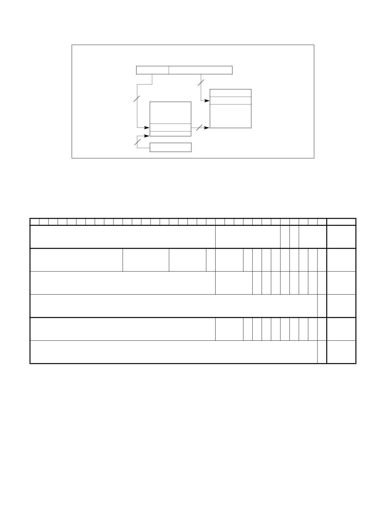
PAGING
Linear Address
31
22 21
0
Directory
Offset
22
4-MByte Page
Page Directory
10
Physical Address
PDE with PS=1
18
32
CR3
Figure 5-3. Linear-Address Translation to a 4-MByte Page using 32-Bit Paging
Figure 5-4 gives a summary of the formats of CR3 and the paging-structure entries with 32-bit paging. For the
paging structure entries, it identifies separately the format of entries that map pages, those that reference other
paging structures, and those that do neither because they are “not present”; bit 0 (P) and bit 7 (PS) are high-
lighted because they determine how such an entry is used.
31
30
29
28
27
26
25
24
23
22
21
20
19
18
17
16
15
14
13
12
11
10
9
8
7
6
5
4
3
2
1
0
P
P
Address of page directory1
Ignored
C
W
Ignored
CR3
D
T
P
P
P
U
R
PDE:
Bits 31:22 of address
Reserved
Bits 39:32 of
A
Ignored
G
1
D
A
C
W
/
/
1
4MB
of 4MB page frame
(must be 0)
address2
T
D
T
S
W
page
I
P
P
U
R
PDE:
Address of page table
Ignored
0
g
A
C
W
/
/
1
page
n
D
T
S
W
table
PDE:
Ignored
0
not
present
P
P
P
U
R
PTE:
Address of 4KB page frame
Ignored
G
A
D
A
C
W
/
/
1
4KB
T
D
T
S
W
page
PTE:
Ignored
0
not
present
Figure 5-4. Formats of CR3 and Paging-Structure Entries with 32-Bit Paging
NOTES:
1. CR3 has 64 bits on processors supporting the Intel-64 architecture. These bits are ignored with 32-bit paging.
2. This example illustrates a processor in which MAXPHYADDR is 36. If this value is larger or smaller, the number of bits reserved in
positions 20:13 of a PDE mapping a 4-MByte page will change.
Vol. 3A
5-11

PAGING
Table 5-3. Use of CR3 with 32-Bit Paging
Bit
Contents
Position(s)
2:0
Ignored
3 (PWT)
Page-level write-through; indirectly determines the memory type used to access the page directory during linear-
address translation (see Section 5.9)
4 (PCD)
Page-level cache disable; indirectly determines the memory type used to access the page directory during linear-
address translation (see Section 5.9)
11:5
Ignored
31:12
Physical address of the 4-KByte aligned page directory used for linear-address translation
63:32
Ignored (these bits exist only on processors supporting the Intel-64 architecture)
Table 5-4. Format of a 32-Bit Page-Directory Entry that Maps a 4-MByte Page
Bit
Contents
Position(s)
0 (P)
Present; must be 1 to map a 4-MByte page
1 (R/W)
Read/write; if 0, writes may not be allowed to the 4-MByte page referenced by this entry (see Section 5.6)
2 (U/S)
User/supervisor; if 0, user-mode accesses are not allowed to the 4-MByte page referenced by this entry (see Section
5.6)
3 (PWT)
Page-level write-through; indirectly determines the memory type used to access the 4-MByte page referenced by
this entry (see Section 5.9)
4 (PCD)
Page-level cache disable; indirectly determines the memory type used to access the 4-MByte page referenced by
this entry (see Section 5.9)
5 (A)
Accessed; indicates whether software has accessed the 4-MByte page referenced by this entry (see Section 5.8)
6 (D)
Dirty; indicates whether software has written to the 4-MByte page referenced by this entry (see Section 5.8)
7 (PS)
Page size; must be 1 (otherwise, this entry references a page table; see Table 5-5)
8 (G)
Global; if CR4.PGE = 1, determines whether the translation is global (see Section 5.10); ignored otherwise
11:9
Ignored
12 (PAT)
If the PAT is supported, indirectly determines the memory type used to access the 4-MByte page referenced by this
entry (see Section 5.9.2); otherwise, reserved (must be 0)1
M-20:13
Bits M-1:32 of physical address of the 4-MByte page referenced by this entry2
21:M-19
Reserved (must be 0)
31:22
Bits 31:22 of physical address of the 4-MByte page referenced by this entry
NOTES:
1. See Section 5.1.4 for how to determine whether the PAT is supported.
2. If the PSE-36 mechanism is not supported, M is 32, and this row does not apply. If the PSE-36 mechanism is supported, M is the min-
imum of 40 and MAXPHYADDR (this row does not apply if MAXPHYADDR = 32). See Section 5.1.4 for how to determine MAXPHY-
ADDR and whether the PSE-36 mechanism is supported.
5-12
Vol. 3A

PAGING
Table 5-5. Format of a 32-Bit Page-Directory Entry that References a Page Table
Bit
Contents
Position(s)
0 (P)
Present; must be 1 to reference a page table
1 (R/W)
Read/write; if 0, writes may not be allowed to the 4-MByte region controlled by this entry (see Section 5.6)
2 (U/S)
User/supervisor; if 0, user-mode accesses are not allowed to the 4-MByte region controlled by this entry (see Section
5.6)
3 (PWT)
Page-level write-through; indirectly determines the memory type used to access the page table referenced by this
entry (see Section 5.9)
4 (PCD)
Page-level cache disable; indirectly determines the memory type used to access the page table referenced by this
entry (see Section 5.9)
5 (A)
Accessed; indicates whether this entry has been used for linear-address translation (see Section 5.8)
6
Ignored
7 (PS)
If CR4.PSE = 1, must be 0 (otherwise, this entry maps a 4-MByte page; see Table 5-4); otherwise, ignored
11:8
Ignored
31:12
Physical address of 4-KByte aligned page table referenced by this entry
Table 5-6. Format of a 32-Bit Page-Table Entry that Maps a 4-KByte Page
Bit
Contents
Position(s)
0 (P)
Present; must be 1 to map a 4-KByte page
1 (R/W)
Read/write; if 0, writes may not be allowed to the 4-KByte page referenced by this entry (see Section 5.6)
2 (U/S)
User/supervisor; if 0, user-mode accesses are not allowed to the 4-KByte page referenced by this entry (see Section
5.6)
3 (PWT)
Page-level write-through; indirectly determines the memory type used to access the 4-KByte page referenced by this
entry (see Section 5.9)
4 (PCD)
Page-level cache disable; indirectly determines the memory type used to access the 4-KByte page referenced by this
entry (see Section 5.9)
5 (A)
Accessed; indicates whether software has accessed the 4-KByte page referenced by this entry (see Section 5.8)
6 (D)
Dirty; indicates whether software has written to the 4-KByte page referenced by this entry (see Section 5.8)
7 (PAT)
If the PAT is supported, indirectly determines the memory type used to access the 4-KByte page referenced by this
entry (see Section 5.9.2); otherwise, reserved (must be 0)1
8 (G)
Global; if CR4.PGE = 1, determines whether the translation is global (see Section 5.10); ignored otherwise
11:9
Ignored
31:12
Physical address of the 4-KByte page referenced by this entry
NOTES:
1. See Section 5.1.4 for how to determine whether the PAT is supported.
Vol. 3A
5-13

PAGING
5.4
PAE PAGING
A logical processor uses PAE paging if CR0.PG = 1, CR4.PAE = 1, and IA32_EFER.LME = 0. PAE paging translates
32-bit linear addresses to 52-bit physical addresses.1 Although 52 bits corresponds to 4 PBytes, linear addresses
are limited to 32 bits; at most 4 GBytes of linear-address space may be accessed at any given time.
With PAE paging, a logical processor maintains a set of four (4) PDPTE registers, which are loaded from an address
in CR3. Linear address are translated using 4 hierarchies of in-memory paging structures, each located using one
of the PDPTE registers. (This is different from the other paging modes, in which there is one hierarchy referenced
by CR3.)
Section 5.4.1 discusses the PDPTE registers. Section 5.4.2 describes linear-address translation with PAE paging.
5.4.1
PDPTE Registers
When PAE paging is used, CR3 references the base of a 32-Byte page-directory-pointer table. Table 5-7 illus-
trates how CR3 is used with PAE paging.
Table 5-7. Use of CR3 with PAE Paging
Bit
Contents
Position(s)
4:0
Ignored
31:5
Physical address of the 32-Byte aligned page-directory-pointer table used for linear-address translation
63:32
Ignored (these bits exist only on processors supporting the Intel-64 architecture)
The page-directory-pointer-table comprises four (4) 64-bit entries called PDPTEs. Each PDPTE controls access to a
1-GByte region of the linear-address space. Corresponding to the PDPTEs, the logical processor maintains a set of
four (4) internal, non-architectural PDPTE registers, called PDPTE0, PDPTE1, PDPTE2, and PDPTE3. The logical
processor loads these registers from the PDPTEs in memory as part of certain operations:
• If PAE paging would be in use following an execution of MOV to CR0 or MOV to CR4 (see Section 5.1.1) and the
instruction is modifying any of CR0.CD, CR0.NW, CR0.PG, CR4.PAE, CR4.PGE, CR4.PSE, or CR4.SMEP; then the
PDPTEs are loaded from the address in CR3.
• If MOV to CR3 is executed while the logical processor is using PAE paging, the PDPTEs are loaded from the
address being loaded into CR3.
• If PAE paging is in use and a task switch changes the value of CR3, the PDPTEs are loaded from the address in
the new CR3 value.
• Certain VMX transitions load the PDPTE registers. See Section 5.11.1.
Table 5-8 gives the format of a PDPTE. If any of the PDPTEs sets both the P flag (bit 0) and any reserved bit, the
MOV to CR instruction causes a general-protection exception (#GP(0)) and the PDPTEs are not loaded.2 As shown
in Table 5-8, bits 2:1, 8:5, and 63:MAXPHYADDR are reserved in the PDPTEs.
1. If MAXPHYADDR < 52, bits in the range 51:MAXPHYADDR will be 0 in any physical address used by PAE paging. (The corresponding
bits are reserved in the paging-structure entries.) See Section 5.1.4 for how to determine MAXPHYADDR.
2. On some processors, reserved bits are checked even in PDPTEs in which the P flag (bit 0) is 0.
5-14
Vol. 3A

PAGING
Table 5-8. Format of a PAE Page-Directory-Pointer-Table Entry (PDPTE)
Bit
Contents
Position(s)
0 (P)
Present; must be 1 to reference a page directory
2:1
Reserved (must be 0)
3 (PWT)
Page-level write-through; indirectly determines the memory type used to access the page directory referenced by
this entry (see Section 5.9)
4 (PCD)
Page-level cache disable; indirectly determines the memory type used to access the page directory referenced by
this entry (see Section 5.9)
8:5
Reserved (must be 0)
11:9
Ignored
M-1:12
Physical address of 4-KByte aligned page directory referenced by this entry1
63:M
Reserved (must be 0)
NOTES:
1. If EPT is not enabled, M is an abbreviation for MAXPHYADDR. If EPT is enabled, M represents the value returned by
CPUID.80000008H:EAX[7:0]. See Section 5.1.4.
5.4.2
Linear-Address Translation with PAE Paging
PAE paging may map linear addresses to either 4-KByte pages or 2-MByte pages. Figure 5-5 illustrates the trans-
lation process when it produces a 4-KByte page; Figure 5-6 covers the case of a 2-MByte page. The following items
describe the PAE paging process in more detail as well has how the page size is determined:
• Bits 31:30 of the linear address select a PDPTE register (see Section 5.4.1); this is PDPTEi, where i is the value
of bits 31:30.1 Because a PDPTE register is identified using bits 31:30 of the linear address, it controls access
to a 1-GByte region of the linear-address space. If the P flag (bit 0) of PDPTEi is 0, the processor ignores bits
63:1, and there is no mapping for the 1-GByte region controlled by PDPTEi. A reference using a linear address
in this region causes a page-fault exception (see Section 5.7).
• If the P flag of PDPTEi is 1, 4-KByte naturally aligned page directory is located at the physical address specified
in bits 51:12 of PDPTEi (see Table 5-8 in Section 5.4.1). A page directory comprises 512 64-bit entries (PDEs).
A PDE is selected using the physical address defined as follows:
- Bits 51:12 are from PDPTEi.
- Bits 11:3 are bits 29:21 of the linear address.
- Bits 2:0 are 0.
Because a PDE is identified using bits 31:21 of the linear address, it controls access to a 2-Mbyte region of the
linear-address space. Use of the PDE depends on its PS flag (bit 7):
• If the PDE’s PS flag is 1, the PDE maps a 2-MByte page (see Table 5-9). The final physical address is computed
as follows:
- Bits 51:21 are from the PDE.
- Bits 20:0 are from the original linear address.
• If the PDE’s PS flag is 0, a 4-KByte naturally aligned page table is located at the physical address specified in
bits 51:12 of the PDE (see Table 5-10). A page table comprises 512 64-bit entries (PTEs). A PTE is selected
using the physical address defined as follows:
1. With PAE paging, the processor does not use CR3 when translating a linear address (as it does in the other paging modes). It does
not access the PDPTEs in the page-directory-pointer table during linear-address translation.
Vol. 3A
5-15
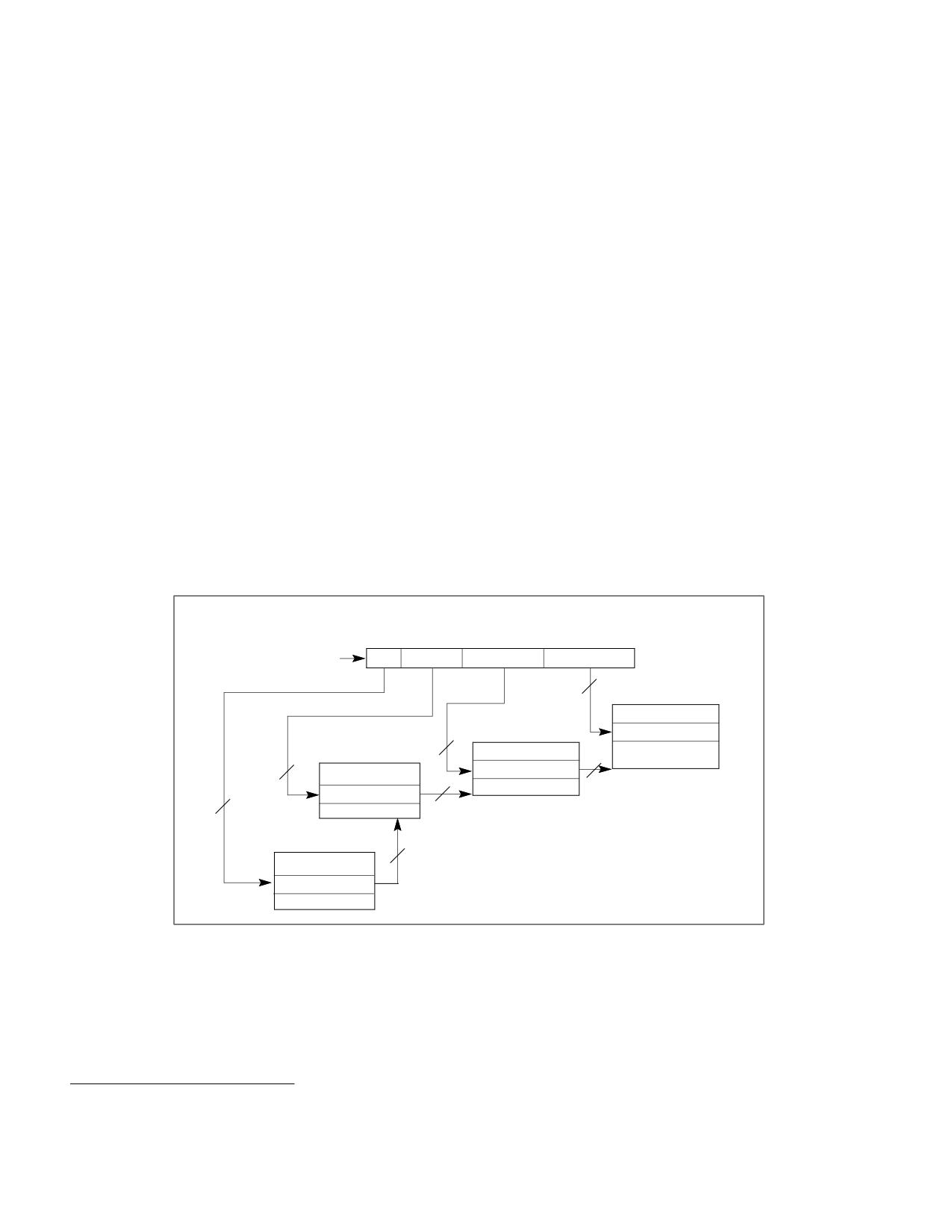
PAGING
- Bits 51:12 are from the PDE.
- Bits 11:3 are bits 20:12 of the linear address.
- Bits 2:0 are 0.
• Because a PTE is identified using bits 31:12 of the linear address, every PTE maps a 4-KByte page (see
Table 5-11). The final physical address is computed as follows:
- Bits 51:12 are from the PTE.
- Bits 11:0 are from the original linear address.
If the P flag (bit 0) of a PDE or a PTE is 0 or if a PDE or a PTE sets any reserved bit, the entry is used neither to
reference another paging-structure entry nor to map a page. There is no translation for a linear address whose
translation would use such a paging-structure entry; a reference to such a linear address causes a page-fault
exception (see Section 5.7).
The following bits are reserved with PAE paging:
• If the P flag (bit 0) of a PDE or a PTE is 1, bits 62:M are reserved, where M is MAXPHYADDR (unless EPT is
enabled, in which case M is the value enumerated by CPUID.80000008H:EAX[7:0]). See Section 5.1.4.
• If the P flag and the PS flag (bit 7) of a PDE are both 1, bits 20:13 are reserved.
• If IA32_EFER.NXE = 0 and the P flag of a PDE or a PTE is 1, the XD flag (bit 63) is reserved.
• If the PAT is not supported:1
- If the P flag of a PTE is 1, bit 7 is reserved.
- If the P flag and the PS flag of a PDE are both 1, bit 12 is reserved.
A reference using a linear address that is successfully translated to a physical address is performed only if allowed
by the access rights of the translation; see Section 5.6.
Linear Address
31
30 29
21 20
12 11
0
Directory Pointer
Directory
Table
Offset
12
4-KByte Page
Page Table
Physical Address
Page Directory
9
PTE
9
40
PDE with PS=0
2
40
PDPTE Registers
40
PDPTE value
Figure 5-5. Linear-Address Translation to a 4-KByte Page using PAE Paging
1. See Section 5.1.4 for how to determine whether the PAT is supported.
5-16
Vol. 3A
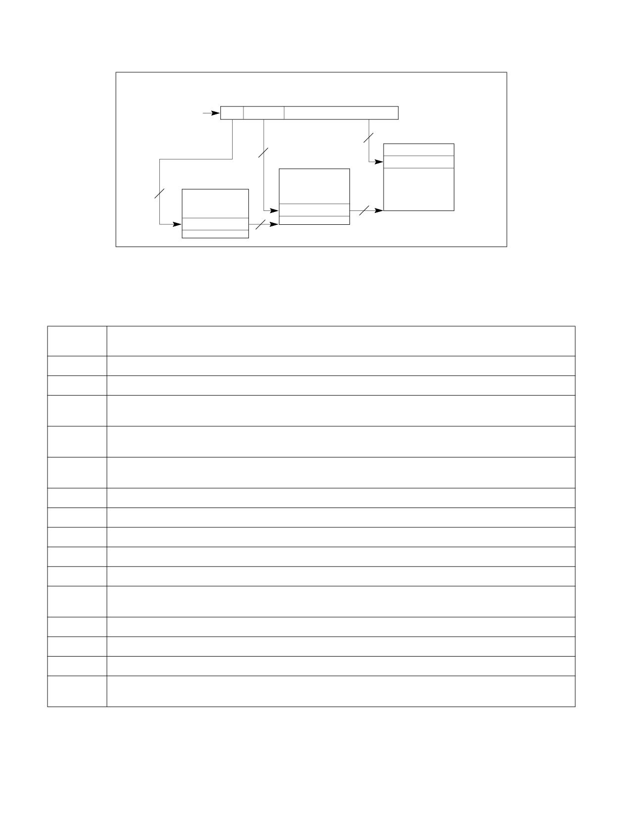
PAGING
Linear Address
31
30 29
21 20
0
Directory
Directory
Offset
Pointer
2-MByte Page
21
9
Page Directory
Physical Address
PDPTE Registers
2
PDE with PS=1
31
PDPTE value
40
Figure 5-6. Linear-Address Translation to a 2-MByte Page using PAE Paging
Table 5-9. Format of a PAE Page-Directory Entry that Maps a 2-MByte Page
Bit
Contents
Position(s)
0 (P)
Present; must be 1 to map a 2-MByte page
1 (R/W)
Read/write; if 0, writes may not be allowed to the 2-MByte page referenced by this entry (see Section 5.6)
2 (U/S)
User/supervisor; if 0, user-mode accesses are not allowed to the 2-MByte page referenced by this entry (see Section
5.6)
3 (PWT)
Page-level write-through; indirectly determines the memory type used to access the 2-MByte page referenced by
this entry (see Section 5.9)
4 (PCD)
Page-level cache disable; indirectly determines the memory type used to access the 2-MByte page referenced by this
entry (see Section 5.9)
5 (A)
Accessed; indicates whether software has accessed the 2-MByte page referenced by this entry (see Section 5.8)
6 (D)
Dirty; indicates whether software has written to the 2-MByte page referenced by this entry (see Section 5.8)
7 (PS)
Page size; must be 1 (otherwise, this entry references a page table; see Table 5-10)
8 (G)
Global; if CR4.PGE = 1, determines whether the translation is global (see Section 5.10); ignored otherwise
11:9
Ignored
12 (PAT)
If the PAT is supported, indirectly determines the memory type used to access the 2-MByte page referenced by this
entry (see Section 5.9.2); otherwise, reserved (must be 0)1
20:13
Reserved (must be 0)
M-1:21
Physical address of the 2-MByte page referenced by this entry2
62:M
Reserved (must be 0)
63 (XD)
If IA32_EFER.NXE = 1, execute-disable (if 1, instruction fetches are not allowed from the 2-MByte page controlled by
this entry; see Section 5.6); otherwise, reserved (must be 0)
NOTES:
1. See Section 5.1.4 for how to determine whether the PAT is supported.
Vol. 3A
5-17

PAGING
2. If EPT is not enabled, M is an abbreviation for MAXPHYADDR. If EPT is enabled, M represents the value returned by
CPUID.80000008H:EAX[7:0]. See Section 5.1.4.
Table 5-10. Format of a PAE Page-Directory Entry that References a Page Table
Bit
Contents
Position(s)
0 (P)
Present; must be 1 to reference a page table
1 (R/W)
Read/write; if 0, writes may not be allowed to the 2-MByte region controlled by this entry (see Section 5.6)
2 (U/S)
User/supervisor; if 0, user-mode accesses are not allowed to the 2-MByte region controlled by this entry (see
Section 5.6)
3 (PWT)
Page-level write-through; indirectly determines the memory type used to access the page table referenced by this
entry (see Section 5.9)
4 (PCD)
Page-level cache disable; indirectly determines the memory type used to access the page table referenced by this
entry (see Section 5.9)
5 (A)
Accessed; indicates whether this entry has been used for linear-address translation (see Section 5.8)
6
Ignored
7 (PS)
Page size; must be 0 (otherwise, this entry maps a 2-MByte page; see Table 5-9)
11:8
Ignored
M-1:12
Physical address of 4-KByte aligned page table referenced by this entry1
62:M
Reserved (must be 0)
63 (XD)
If IA32_EFER.NXE = 1, execute-disable (if 1, instruction fetches are not allowed from the 2-MByte region controlled
by this entry; see Section 5.6); otherwise, reserved (must be 0)
NOTES:
1. If EPT is not enabled, M is an abbreviation for MAXPHYADDR. If EPT is enabled, M represents the value returned by
CPUID.80000008H:EAX[7:0]. See Section 5.1.4.
Table 5-11. Format of a PAE Page-Table Entry that Maps a 4-KByte Page
Bit
Contents
Position(s)
0 (P)
Present; must be 1 to map a 4-KByte page
1 (R/W)
Read/write; if 0, writes may not be allowed to the 4-KByte page referenced by this entry (see Section 5.6)
2 (U/S)
User/supervisor; if 0, user-mode accesses are not allowed to the 4-KByte page referenced by this entry (see Section
5.6)
3 (PWT)
Page-level write-through; indirectly determines the memory type used to access the 4-KByte page referenced by
this entry (see Section 5.9)
4 (PCD)
Page-level cache disable; indirectly determines the memory type used to access the 4-KByte page referenced by this
entry (see Section 5.9)
5 (A)
Accessed; indicates whether software has accessed the 4-KByte page referenced by this entry (see Section 5.8)
5-18
Vol. 3A
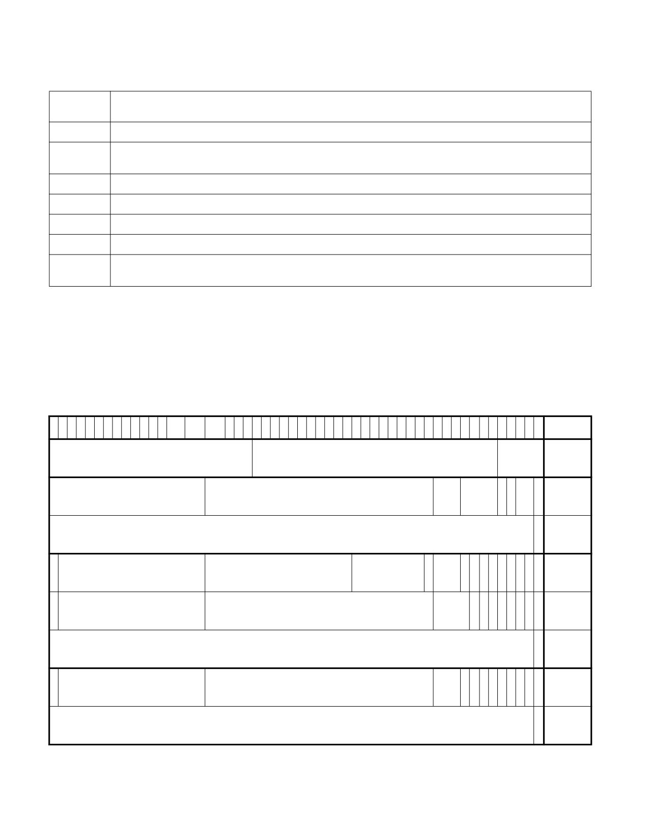
PAGING
Table 5-11. Format of a PAE Page-Table Entry that Maps a 4-KByte Page (Contd.)
Bit
Contents
Position(s)
6 (D)
Dirty; indicates whether software has written to the 4-KByte page referenced by this entry (see Section 5.8)
7 (PAT)
If the PAT is supported, indirectly determines the memory type used to access the 4-KByte page referenced by this
entry (see Section 5.9.2); otherwise, reserved (must be 0)1
8 (G)
Global; if CR4.PGE = 1, determines whether the translation is global (see Section 5.10); ignored otherwise
11:9
Ignored
M-1:12
Physical address of the 4-KByte page referenced by this entry2
62:M
Reserved (must be 0)
63 (XD)
If IA32_EFER.NXE = 1, execute-disable (if 1, instruction fetches are not allowed from the 4-KByte page controlled by
this entry; see Section 5.6); otherwise, reserved (must be 0)
NOTES:
1. See Section 5.1.4 for how to determine whether the PAT is supported.
2. If EPT is not enabled, M is an abbreviation for MAXPHYADDR. If EPT is enabled, M represents the value returned by
CPUID.80000008H:EAX[7:0]. See Section 5.1.4.
Figure 5-7 gives a summary of the formats of CR3 and the paging-structure entries with PAE paging. For the paging
structure entries, it identifies separately the format of entries that map pages, those that reference other paging
structures, and those that do neither because they are “not present”; bit 0 (P) and bit 7 (PS) are highlighted
because they determine how a paging-structure entry is used.
6
6
6
6
5
5
5
5
5
5
5
5
5
3
3
3
2
2
2
2
2
2
2
2
2
2
1
1
1
1
1
1
1
1
1
1
M1
M-1
3
2
1
0
9
8
7
6
5
4
3
2
1
2
1
0
9
8
7
6
5
4
3
2
1
0
9
8
7
6
5
4
3
2
1
0
9
8
7
6
5
4
3
2
1
0
Ignored2
Address of page-directory-pointer table
Ignored
CR3
P
P
Rs
PDPTE:
Reserved3
Address of page directory
Ign.
Rsvd.
C
W
1
vd
present
D
T
PDPTE:
Ignored
0
not
present
X
P
P
P
R
PDE:
Address of
U
D
Reserved
Reserved
A
Ign.
G
1
D
A
C
W
/
1
2MB
4
2MB page frame
/S
T
D
T
W
page
I
P
P
R
PDE:
X
U
Reserved
Address of page table
Ign.
0
g
A
C
W
/
1
page
D
/S
n
D
T
W
table
PDE:
Ignored
0
not
present
P
P
P
R
PTE:
X
U
Reserved
Address of 4KB page frame
Ign.
G
A
D
A
C
W
/
1
4KB
D
/S
T
D
T
W
page
PTE:
Ignored
0
not
present
Figure 5-7. Formats of CR3 and Paging-Structure Entries with PAE Paging
Vol. 3A
5-19
PAGING
NOTES:
1. If EPT is not enabled, M is an abbreviation for MAXPHYADDR. If EPT is enabled, M represents the value returned by
CPUID.80000008H:EAX[7:0]. See Section 5.1.4.
2. CR3 has 64 bits only on processors supporting the Intel-64 architecture. These bits are ignored with PAE paging.
3. Reserved fields must be 0.
4. If IA32_EFER.NXE = 0 and the P flag of a PDE or a PTE is 1, the XD flag (bit 63) is reserved.
5.5
4-LEVEL PAGING AND 5-LEVEL PAGING
Because the operation of 4-level paging and 5-level paging is very similar, they are described together in this
section. The following items highlight the distinctions between the two paging modes:
• A logical processor uses 4-level paging if CR0.PG = 1, CR4.PAE = 1, IA32_EFER.LME = 1, and CR4.LA57 = 0.
4-level paging translates 48-bit linear addresses to 52-bit physical addresses.1 Although 52 bits corresponds to
4 PBytes, linear addresses are limited to 48 bits; at most 256 TBytes of linear-address space may be accessed
at any given time.
• A logical processor uses 5-level paging if CR0.PG = 1, CR4.PAE = 1, IA32_EFER.LME = 1, and CR4.LA57 = 1.
5-level paging translates 57-bit linear addresses to 52-bit physical addresses. Thus, 5-level paging supports a
linear-address space sufficient to access the entire physical-address space.
5.5.1
Ordinary Paging and HLAT Paging
There are two forms of 4-level paging and 5-level paging that differ principally with regard to how linear-address
translation identifies the first paging structure.
The normal form is called ordinary paging, and it uses CR3 to locate the first paging structure, similar to what is
done for 32-bit paging. Section 5.5.2 provides details of this use of CR3.
An alternative form of paging may be used with the VMX feature called hypervisor-managed linear-address trans-
lation (HLAT). Called HLAT paging, this form is used only in VMX non-root operation and only if the “enable HLAT”
VM-execution control is 1.2 HLAT paging locates the first paging structure using a VM-execution control field in the
VMCS called the HLAT pointer (HLATP). Section 5.5.3 provides details.
Whether HLAT paging is used to translate a specific linear address depends on the address and on the value of a
VM-execution control field in the VMCS called the HLAT prefix size:
• If the HLAT prefix size is zero, every linear address is translated using HLAT paging.
• If the HLAT prefix size is not zero, a linear address is translated using HLAT paging if bit 63 of the address is 1.3
The address is translated using ordinary paging if bit 63 of the address is 0.
In some cases, HLAT paging may specify that a translation of a linear address must be restarted. When this occurs,
the linear address is then translated using ordinary paging (starting with a paging structure identified using CR3).
The situations leading to this restart are detailed in Section 5.5.4, and additional details of the restart process are
given in Section 5.5.5.
1. If MAXPHYADDR < 52, bits in the range 51:MAXPHYADDR will be 0 in any physical address used by 4-level paging or 5-level paging.
(The corresponding bits are reserved in the paging-structure entries.) See Section 5.1.4 for how to determine MAXPHYADDR.
2. HLAT paging is used only with 4-level paging and 5-level paging. It is never used with 32-bit paging or PAE paging, regardless of the
value of the “enable HLAT” VM-execution control.
3. This behavior applies if the CPU enumerates a maximum HLAT prefix size of 1 in IA32_VMX_EPT_VPID_CAP[53:48] (see Appendix
A.10). Behavior when a different value is enumerated is not currently defined.
5-20
Vol. 3A

PAGING
5.5.2
Use of CR3 with Ordinary 4-Level Paging and 5-Level Paging
Ordinary 4-level paging and 5-level paging each translate linear addresses using a hierarchy of in-memory paging
structures located using the contents of CR3, which is used to locate the first paging structure. For 4-level paging,
this is the PML4 table, and for 5-level paging it is the PML5 table. Use of CR3 with 4-level paging and 5-level paging
depends on whether process-context identifiers (PCIDs) have been enabled by setting CR4.PCIDE:
• Table 5-12 illustrates how CR3 is used with 4-level paging and 5-level paging if CR4.PCIDE = 0.
Table 5-12. Use of CR3 with 4-Level Paging and 5-level Paging and CR4.PCIDE = 0
Bit
Contents
Position(s)
2:0
Ignored
3 (PWT)
Page-level write-through; indirectly determines the memory type used to access the PML4 table or PML5 table
during linear-address translation (see Section 5.9.2)
4 (PCD)
Page-level cache disable; indirectly determines the memory type used to access the PML4 table or PML5 table during
linear-address translation (see Section 5.9.2)
11:5
Ignored
M-1:12
Physical address of the 4-KByte aligned PML4 table or PML5 table used for linear-address translation1
60:M
Reserved (must be 0)
61
Enables LAM57 for user pointers; Section 4.4.2
62
Enables LAM48 for user pointers; ignored if bit 61 is set.2
63
Reserved (must be 0)3
NOTES:
1. If EPT is not enabled, M is an abbreviation for MAXPHYADDR. If EPT is enabled, M represents the value returned by
CPUID.80000008H:EAX[7:0]. See Section 5.1.4.
2. LAM is not a paging feature.
3. See Section 5.10.4.1 for use of bit 63 of the source operand of the MOV to CR3 instruction.
• Table 5-13 illustrates how CR3 is used with 4-level paging and 5-level paging if CR4.PCIDE = 1.
Table 5-13. Use of CR3 with 4-Level Paging and 5-Level Paging and CR4.PCIDE = 1
Bit
Contents
Position(s)
11:0
PCID (see Section 5.10.1)1
M-1:12
Physical address of the 4-KByte aligned PML4 table used for linear-address translation2
60:M
Reserved (must be 0)
61
Enables LAM57 for user pointers; Section 4.4.3
62
Enables LAM48 for user pointers; ignored if bit 61 is set.3
63
Reserved (must be 0)4
NOTES:
1. Section 5.9.2 explains how the processor determines the memory type used to access the PML4 table during linear-address transla-
tion with CR4.PCIDE = 1.
Vol. 3A
5-21
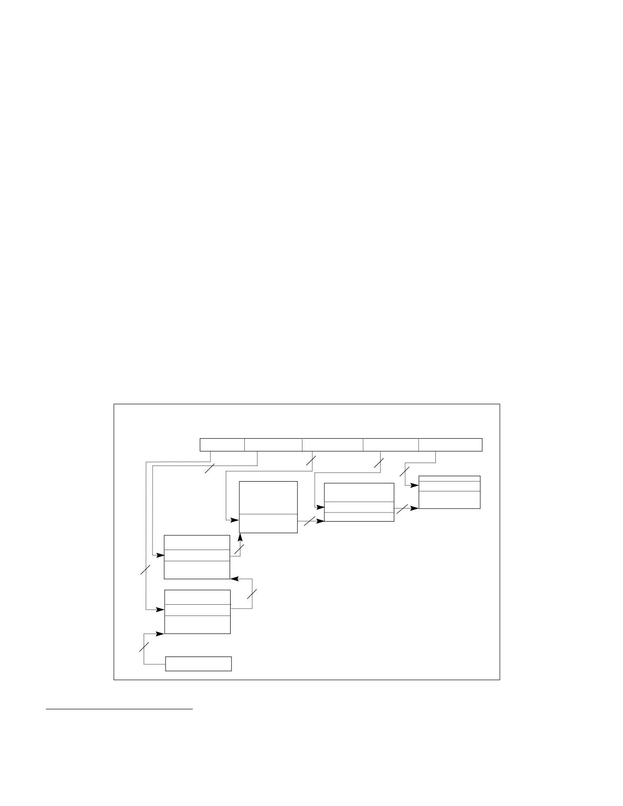
PAGING
2. If EPT is not enabled, M is an abbreviation for MAXPHYADDR. If EPT is enabled, M represents the value returned by
CPUID.80000008H:EAX[7:0]. See Section 5.1.4.
3. LAM is not a paging feature.
4. See Section 5.10.4.1 for use of bit 63 of the source operand of the MOV to CR3 instruction.
After software modifies the value of CR4.PCIDE, the logical processor immediately begins using CR3 as specified for
the new value. For example, if software changes CR4.PCIDE from 1 to 0, the current PCID immediately changes
from CR3[11:0] to 000H (see also Section 5.10.4.1). In addition, the logical processor subsequently determines
the memory type used to access the PML4 table using CR3.PWT and CR3.PCD, which had been bits 4:3 of the PCID.
5.5.3
Use of HLATP with HLAT 4-Level Paging and 5-Level Paging
With HLAT paging, 4-level paging and 5-level paging each translate linear addresses using a hierarchy of in-
memory paging structures located using the value of HLATP (a VM-execution control field in the VMCS), which is
used to locate the first paging structure. For 4-level paging, this is the PML4 table, and for 5-level paging it is the
PML5 table.
HLATP has the same format as that given for CR3 in Table 5-12, with the exception that bits 2:0 and bits 11:5 are
reserved and must be zero (these bits are checked by VM entry). HLATP does not contain a PCID value. HLAT
paging with CR4.PCIDE = 1 uses the PCID value in CR3[11:0].
5.5.4
Linear-Address Translation with 4-Level Paging and 5-Level Paging
4-level paging and 5-level paging may map linear addresses to 4-KByte pages, 2-MByte pages, or 1-GByte pages.1
Figure 5-8 illustrates the translation process for 4-level paging when it produces a 4-KByte page; Figure 5-9 covers
the case of a 2-MByte page, and Figure 5-10 the case of a 1-GByte page. (The process for 5-level paging is similar.)
Linear Address
47
39 38
30 29
21 20
12
11
0
PML4
Directory Ptr
Directory
Table
Offset
9
9
9
4-KByte Page
12
Physical Addr
PTE
40
Page-Directory-
PDE with PS=0
Pointer Table
40
Page Table
Page-Directory
40
PDPTE
9
40
PML4E
40
CR3 or HLATP
Figure 5-8. Linear-Address Translation to a 4-KByte Page Using 4-Level Paging
1. Not all processors support 1-GByte pages; see Section 5.1.4.
5-22
Vol. 3A
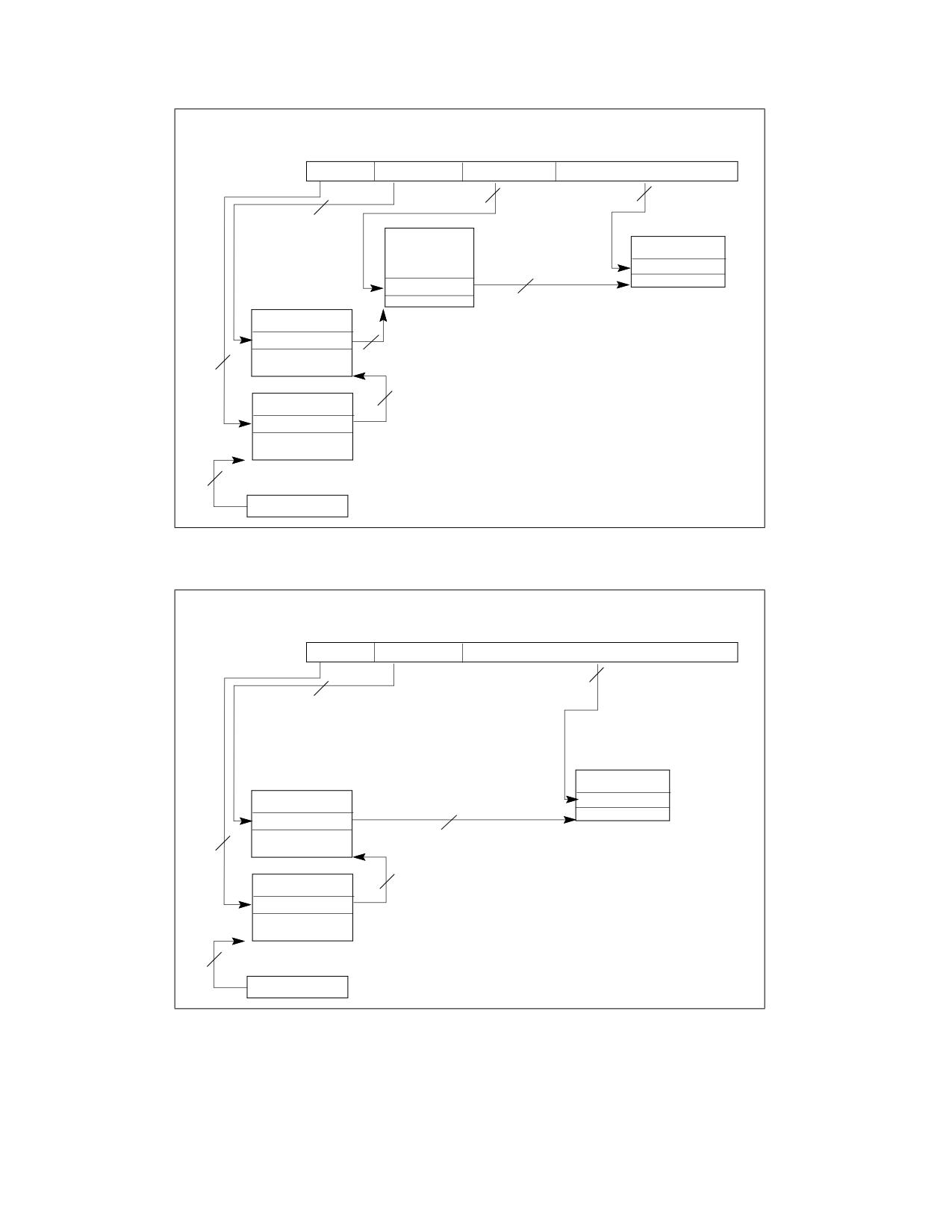
PAGING
Linear Address
47
39 38
30 29
21
20
0
PML4
Directory Ptr
Directory
Offset
21
9
9
2-MByte Page
Physical Addr
Page-Directory-
PDE with PS=1
Pointer Table
31
Page-Directory
PDPTE
40
9
40
PML4E
40
CR3 or HLATP
Figure 5-9. Linear-Address Translation to a 2-MByte Page using 4-Level Paging
Linear Address
47
39 38
30 29
0
PML4
Directory Ptr
Offset
30
9
1-GByte Page
Page-Directory-
Pointer Table
Physical Addr
PDPTE with PS=1
22
9
40
PML4E
40
CR3 or HLATP
Figure 5-10. Linear-Address Translation to a 1-GByte Page using 4-Level Paging
Vol. 3A
5-23
PAGING
4-level paging and 5-level paging associate with each linear address a protection key. Section 5.6 explains how
the processor uses the protection key in its determination of the access rights of each linear address.
The remainder of this section describes the translation process used by 4-level paging and 5-level paging in more
detail, as well has how the page size and protection key are determined. Because the process used by the two
paging modes is similar, they are described together, with any differences identified, in the following items:
• With 5-level paging, a 4-KByte naturally aligned PML5 table is located at the physical address specified in
bits 51:12 of CR3 (see Table 5-12). (4-level paging does not use a PML5 table and omits this step.) A PML5
table comprises 512 64-bit entries (PML5Es). A PML5E is selected using the physical address defined as follows:
- Bits 51:12 are from CR3 or HLATP.
- Bits 11:3 are bits 56:48 of the linear address.
- Bits 2:0 are all 0.
Because a PML5E is identified using bits 56:48 of the linear address, it controls access to a 256-TByte region of
the linear-address space.
With HLAT paging, if bit 11 of the PML5E is 1, translation is restarted with ordinary paging with a maximum
page size of 256-TBytes (see Section 5.5.5). Otherwise, the translation process continues as described in the
next item.
• A 4-KByte naturally aligned PML4 table is located at the physical address specified in bits 51:12 of CR3 (for 4-
level paging; see Table 5-12) or in bits 51:12 of the PML5E (for 5-level paging; see Table 5-14). A PML4 table
comprises 512 64-bit entries (PML4Es). A PML4E is selected using the physical address defined as follows:
- Bits 51:12 are from CR3 or the HLATP (for 4-level paging) or in bits 51:12 of the PML5E (for 5-level
paging).
- Bits 11:3 are bits 47:39 of the linear address.
- Bits 2:0 are all 0.
Because a PML4E is identified using bits 47:39 of the linear address, it controls access to a 512-GByte region of
the linear-address space.
With HLAT paging, if bit 11 of the PML4E is 1, translation is restarted with ordinary paging with a maximum
page size of 512-GBytes (see Section 5.5.5). Otherwise, the translation process continues as described in the
next item.
• A 4-KByte naturally aligned page-directory-pointer table is located at the physical address specified in
bits 51:12 of the PML4E (see Table 5-15). A page-directory-pointer table comprises 512 64-bit entries
(PDPTEs). A PDPTE is selected using the physical address defined as follows:
- Bits 51:12 are from the PML4E.
- Bits 11:3 are bits 38:30 of the linear address.
- Bits 2:0 are all 0.
Because a PDPTE is identified using bits 47:30 of the linear address, it controls access to a 1-GByte region of the
linear-address space.
With HLAT paging, if bit 11 of the PDPTE is 1, translation is restarted with ordinary paging with a maximum page
size of 1-GByte (see Section 5.5.5). Otherwise, the translation process continues as described below.
Use of the PDPTE depends on its PS flag (bit 7):1
• If the PDPTE’s PS flag is 1, the PDPTE maps a 1-GByte page (see Table 5-16). The final physical address is
computed as follows:
- Bits 51:30 are from the PDPTE.
- Bits 29:0 are from the original linear address.
The linear address’s protection key is the value of bits 62:59 of the PDPTE (see Section 5.6.2).
1. The PS flag of a PDPTE is reserved and must be 0 (if the P flag is 1) if 1-GByte pages are not supported. See Section 5.1.4 for how
to determine whether 1-GByte pages are supported.
5-24
Vol. 3A
PAGING
• If the PDPTE’s PS flag is 0, a 4-KByte naturally aligned page directory is located at the physical address
specified in bits 51:12 of the PDPTE (see Table 5-17). A page directory comprises 512 64-bit entries (PDEs). A
PDE is selected using the physical address defined as follows:
- Bits 51:12 are from the PDPTE.
- Bits 11:3 are bits 29:21 of the linear address.
- Bits 2:0 are all 0.
Because a PDE is identified using bits 47:21 of the linear address, it controls access to a 2-MByte region of the
linear-address space.
With HLAT paging, if bit 11 of the PDE is 1, translation is restarted with ordinary paging with a maximum page size
of 2-MBytes (see Section 5.5.5). Otherwise, the translation process continues as described below.
Use of the PDE depends on its PS flag:
• If the PDE's PS flag is 1, the PDE maps a 2-MByte page (see Table 5-18). The final physical address is computed
as follows:
- Bits 51:21 are from the PDE.
- Bits 20:0 are from the original linear address.
The linear address’s protection key is the value of bits 62:59 of the PDE (see Section 5.6.2).
• If the PDE’s PS flag is 0, a 4-KByte naturally aligned page table is located at the physical address specified in
bits 51:12 of the PDE (see Table 5-19). A page table comprises 512 64-bit entries (PTEs). A PTE is selected
using the physical address defined as follows:
- Bits 51:12 are from the PDE.
- Bits 11:3 are bits 20:12 of the linear address.
- Bits 2:0 are all 0.
• Because a PTE is identified using bits 47:12 of the linear address, every PTE maps a 4-KByte page (see
Table 5-20).
With HLAT paging, if bit 11 of the PTE is 1, translation is restarted with ordinary paging with a maximum page
size of 4-KBytes (see Section 5.5.5). Otherwise, the final physical address is computed as follows:
- Bits 51:12 are from the PTE.
- Bits 11:0 are from the original linear address.
The linear address’s protection key is the value of bits 62:59 of the PTE (see Section 5.6.2).
If a paging-structure entry’s P flag (bit 0) is 0 or if the entry sets any reserved bit, the entry is used neither to refer-
ence another paging-structure entry nor to map a page. There is no translation for a linear address whose transla-
tion would use such a paging-structure entry; a reference to such a linear address causes a page-fault exception
(see Section 5.7).
The following bits in a paging-structure entry are reserved with 4-level paging and 5-level paging (assuming that
the entry’s P flag is 1):
• Bits 51:M are reserved in every paging-structure entry, where M is MAXPHYADDR (unless EPT is enabled, in
which case it is the value enumerated by CPUID.80000008H:EAX[7:0]). See Section 5.1.4.
• The PS flag is reserved in a PML5E or a PML4E.
• If 1-GByte pages are not supported, the PS flag is reserved in a PDPTE.1
• If the PS flag in a PDPTE is 1, bits 29:13 of the entry are reserved.
• If the PS flag in a PDE is 1, bits 20:13 of the entry are reserved.
• If IA32_EFER.NXE = 0, the XD flag (bit 63) is reserved in every paging-structure entry.
A reference using a linear address that is successfully translated to a physical address is performed only if allowed
by the access rights of the translation; see Section 5.6.
1. See Section 5.1.4 for how to determine whether 1-GByte pages are supported.
Vol. 3A
5-25

PAGING
Figure 5-11 gives a summary of the formats of CR3 and the 4-level and 5-level paging-structure entries. For the
paging structure entries, it identifies separately the format of entries that map pages, those that reference other
paging structures, and those that do neither because they are “not present”; bit 0 (P) and bit 7 (PS) are highlighted
because they determine how a paging-structure entry is used.
Table 5-14. Format of a PML5 Entry (PML5E) that References a PML4 Table
Bit
Contents
Position(s)
0 (P)
Present; must be 1 to reference a PML4 table
1 (R/W)
Read/write; if 0, writes may not be allowed to the 256-TByte region controlled by this entry (see Section 5.6)
2 (U/S)
User/supervisor; if 0, user-mode accesses are not allowed to the 256-TByte region controlled by this entry (see
Section 5.6)
3 (PWT)
Page-level write-through; indirectly determines the memory type used to access the PML4 table referenced by this
entry (see Section 5.9.2)
4 (PCD)
Page-level cache disable; indirectly determines the memory type used to access the PML4 table referenced by this
entry (see Section 5.9.2)
5 (A)
Accessed; indicates whether this entry has been used for linear-address translation (see Section 5.8)
6
Ignored
7 (PS)
Reserved (must be 0)
10:8
Ignored
11 (R)
For ordinary paging, ignored; for HLAT paging, restart (if 1, linear-address translation is restarted with ordinary
paging)
M-1:12
Physical address of 4-KByte aligned PML4 table referenced by this entry1
51:M
Reserved (must be 0)
62:52
Ignored
63 (XD)
If IA32_EFER.NXE = 1, execute-disable (if 1, instruction fetches are not allowed from the 256-TByte region
controlled by this entry; see Section 5.6); otherwise, reserved (must be 0)
NOTES:
1. If EPT is not enabled, M is an abbreviation for MAXPHYADDR. If EPT is enabled, M represents the value returned by
CPUID.80000008H:EAX[7:0]. See Section 5.1.4.
Table 5-15. Format of a PML4 Entry (PML4E) that References a Page-Directory-Pointer Table
Bit
Contents
Position(s)
0 (P)
Present; must be 1 to reference a page-directory-pointer table
1 (R/W)
Read/write; if 0, writes may not be allowed to the 512-GByte region controlled by this entry (see Section 5.6)
2 (U/S)
User/supervisor; if 0, user-mode accesses are not allowed to the 512-GByte region controlled by this entry (see
Section 5.6)
3 (PWT)
Page-level write-through; indirectly determines the memory type used to access the page-directory-pointer table
referenced by this entry (see Section 5.9.2)
4 (PCD)
Page-level cache disable; indirectly determines the memory type used to access the page-directory-pointer table
referenced by this entry (see Section 5.9.2)
5-26
Vol. 3A

PAGING
Table 5-15. Format of a PML4 Entry (PML4E) that References a Page-Directory-Pointer Table (Contd.)
Bit
Contents
Position(s)
5 (A)
Accessed; indicates whether this entry has been used for linear-address translation (see Section 5.8)
6
Ignored
7 (PS)
Reserved (must be 0)
10:8
Ignored
11 (R)
For ordinary paging, ignored; for HLAT paging, restart (if 1, linear-address translation is restarted with ordinary
paging)
M-1:12
Physical address of 4-KByte aligned page-directory-pointer table referenced by this entry1
51:M
Reserved (must be 0)
62:52
Ignored
63 (XD)
If IA32_EFER.NXE = 1, execute-disable (if 1, instruction fetches are not allowed from the 512-GByte region
controlled by this entry; see Section 5.6); otherwise, reserved (must be 0)
NOTES:
1. If EPT is not enabled, M is an abbreviation for MAXPHYADDR. If EPT is enabled, M represents the value returned by
CPUID.80000008H:EAX[7:0]. See Section 5.1.4.
Table 5-16. Format of a Page-Directory-Pointer-Table Entry (PDPTE) that Maps a 1-GByte Page
Bit
Contents
Position(s)
0 (P)
Present; must be 1 to map a 1-GByte page
1 (R/W)
Read/write; if 0, writes may not be allowed to the 1-GByte page referenced by this entry (see Section 5.6)
2 (U/S)
User/supervisor; if 0, user-mode accesses are not allowed to the 1-GByte page referenced by this entry (see Section
5.6)
3 (PWT)
Page-level write-through; indirectly determines the memory type used to access the 1-GByte page referenced by this
entry (see Section 5.9.2)
4 (PCD)
Page-level cache disable; indirectly determines the memory type used to access the 1-GByte page referenced by this
entry (see Section 5.9.2)
5 (A)
Accessed; indicates whether software has accessed the 1-GByte page referenced by this entry (see Section 5.8)
6 (D)
Dirty; indicates whether software has written to the 1-GByte page referenced by this entry (see Section 5.8)
7 (PS)
Page size; must be 1 (otherwise, this entry references a page directory; see Table 5-17)
8 (G)
Global; if CR4.PGE = 1, determines whether the translation is global (see Section 5.10); ignored otherwise
10:9
Ignored
11 (R)
For ordinary paging, ignored; for HLAT paging, restart (if 1, linear-address translation is restarted with ordinary
paging)
12 (PAT)
Indirectly determines the memory type used to access the 1-GByte page referenced by this entry (see Section
5.9.2)1
29:13
Reserved (must be 0)
Vol. 3A
5-27

PAGING
Table 5-16. Format of a Page-Directory-Pointer-Table Entry (PDPTE) that Maps a 1-GByte Page (Contd.)
Bit
Contents
Position(s)
M-1:30
Physical address of the 1-GByte page referenced by this entry2
51:M
Reserved (must be 0)
58:52
Ignored
62:59
Protection key; if CR4.PKE = 1 or CR4.PKS = 1, this may control the page’s access rights (see Section 5.6.2); otherwise,
it is ignored and not used to control access rights.
63 (XD)
If IA32_EFER.NXE = 1, execute-disable (if 1, instruction fetches are not allowed from the 1-GByte page controlled by
this entry; see Section 5.6); otherwise, reserved (must be 0)
NOTES:
1. The PAT is supported on all processors that support 4-level paging.
2. If EPT is not enabled, M is an abbreviation for MAXPHYADDR. If EPT is enabled, M represents the value returned by
CPUID.80000008H:EAX[7:0]. See Section 5.1.4.
Table 5-17. Format of a Page-Directory-Pointer-Table Entry (PDPTE) that References a Page Directory
Bit
Contents
Position(s)
0 (P)
Present; must be 1 to reference a page directory
1 (R/W)
Read/write; if 0, writes may not be allowed to the 1-GByte region controlled by this entry (see Section 5.6)
2 (U/S)
User/supervisor; if 0, user-mode accesses are not allowed to the 1-GByte region controlled by this entry (see Section
5.6)
3 (PWT)
Page-level write-through; indirectly determines the memory type used to access the page directory referenced by
this entry (see Section 5.9.2)
4 (PCD)
Page-level cache disable; indirectly determines the memory type used to access the page directory referenced by
this entry (see Section 5.9.2)
5 (A)
Accessed; indicates whether this entry has been used for linear-address translation (see Section 5.8)
6
Ignored
7 (PS)
Page size; must be 0 (otherwise, this entry maps a 1-GByte page; see Table 5-16)
10:8
Ignored
11 (R)
For ordinary paging, ignored; for HLAT paging, restart (if 1, linear-address translation is restarted with ordinary
paging)
M-1:12
Physical address of 4-KByte aligned page directory referenced by this entry1
51:M
Reserved (must be 0)
62:52
Ignored
63 (XD)
If IA32_EFER.NXE = 1, execute-disable (if 1, instruction fetches are not allowed from the 1-GByte region controlled
by this entry; see Section 5.6); otherwise, reserved (must be 0)
NOTES:
1. If EPT is not enabled, M is an abbreviation for MAXPHYADDR. If EPT is enabled, M represents the value returned by
CPUID.80000008H:EAX[7:0]. See Section 5.1.4.
5-28
Vol. 3A

PAGING
Table 5-18. Format of a Page-Directory Entry that Maps a 2-MByte Page
Bit
Contents
Position(s)
0 (P)
Present; must be 1 to map a 2-MByte page
1 (R/W)
Read/write; if 0, writes may not be allowed to the 2-MByte page referenced by this entry (see Section 5.6)
2 (U/S)
User/supervisor; if 0, user-mode accesses are not allowed to the 2-MByte page referenced by this entry (see Section
5.6)
3 (PWT)
Page-level write-through; indirectly determines the memory type used to access the 2-MByte page referenced by
this entry (see Section 5.9.2)
4 (PCD)
Page-level cache disable; indirectly determines the memory type used to access the 2-MByte page referenced by
this entry (see Section 5.9.2)
5 (A)
Accessed; indicates whether software has accessed the 2-MByte page referenced by this entry (see Section 5.8)
6 (D)
Dirty; indicates whether software has written to the 2-MByte page referenced by this entry (see Section 5.8)
7 (PS)
Page size; must be 1 (otherwise, this entry references a page table; see Table 5-19)
8 (G)
Global; if CR4.PGE = 1, determines whether the translation is global (see Section 5.10); ignored otherwise
10:9
Ignored
11 (R)
For ordinary paging, ignored; for HLAT paging, restart (if 1, linear-address translation is restarted with ordinary
paging)
12 (PAT)
Indirectly determines the memory type used to access the 2-MByte page referenced by this entry (see Section
5.9.2)
20:13
Reserved (must be 0)
M-1:21
Physical address of the 2-MByte page referenced by this entry1
51:M
Reserved (must be 0)
58:52
Ignored
62:59
Protection key; if CR4.PKE = 1 or CR4.PKS = 1, this may control the page’s access rights (see Section 5.6.2);
otherwise, it is ignored and not used to control access rights.
63 (XD)
If IA32_EFER.NXE = 1, execute-disable (if 1, instruction fetches are not allowed from the 2-MByte page controlled by
this entry; see Section 5.6); otherwise, reserved (must be 0)
NOTES:
1. If EPT is not enabled, M is an abbreviation for MAXPHYADDR. If EPT is enabled, M represents the value returned by
CPUID.80000008H:EAX[7:0]. See Section 5.1.4.
Vol. 3A
5-29

PAGING
Table 5-19. Format of a Page-Directory Entry that References a Page Table
Bit
Contents
Position(s)
0 (P)
Present; must be 1 to reference a page table
1 (R/W)
Read/write; if 0, writes may not be allowed to the 2-MByte region controlled by this entry (see Section 5.6)
2 (U/S)
User/supervisor; if 0, user-mode accesses are not allowed to the 2-MByte region controlled by this entry (see Section
5.6)
3 (PWT)
Page-level write-through; indirectly determines the memory type used to access the page table referenced by this
entry (see Section 5.9.2)
4 (PCD)
Page-level cache disable; indirectly determines the memory type used to access the page table referenced by this
entry (see Section 5.9.2)
5 (A)
Accessed; indicates whether this entry has been used for linear-address translation (see Section 5.8)
6
Ignored
7 (PS)
Page size; must be 0 (otherwise, this entry maps a 2-MByte page; see Table 5-18)
10:8
Ignored
11 (R)
For ordinary paging, ignored; for HLAT paging, restart (if 1, linear-address translation is restarted with ordinary
paging)
M-1:12
Physical address of 4-KByte aligned page table referenced by this entry1
51:M
Reserved (must be 0)
62:52
Ignored
63 (XD)
If IA32_EFER.NXE = 1, execute-disable (if 1, instruction fetches are not allowed from the 2-MByte region controlled
by this entry; see Section 5.6); otherwise, reserved (must be 0)
NOTES:
1. If EPT is not enabled, M is an abbreviation for MAXPHYADDR. If EPT is enabled, M represents the value returned by
CPUID.80000008H:EAX[7:0]. See Section 5.1.4.
5-30
Vol. 3A

PAGING
Table 5-20. Format of a Page-Table Entry that Maps a 4-KByte Page
Bit
Contents
Position(s)
0 (P)
Present; must be 1 to map a 4-KByte page
1 (R/W)
Read/write; if 0, writes may not be allowed to the 4-KByte page referenced by this entry (see Section 5.6)
2 (U/S)
User/supervisor; if 0, user-mode accesses are not allowed to the 4-KByte page referenced by this entry (see Section
5.6)
3 (PWT)
Page-level write-through; indirectly determines the memory type used to access the 4-KByte page referenced by
this entry (see Section 5.9.2)
4 (PCD)
Page-level cache disable; indirectly determines the memory type used to access the 4-KByte page referenced by this
entry (see Section 5.9.2)
5 (A)
Accessed; indicates whether software has accessed the 4-KByte page referenced by this entry (see Section 5.8)
6 (D)
Dirty; indicates whether software has written to the 4-KByte page referenced by this entry (see Section 5.8)
7 (PAT)
Indirectly determines the memory type used to access the 4-KByte page referenced by this entry (see Section 5.9.2)
8 (G)
Global; if CR4.PGE = 1, determines whether the translation is global (see Section 5.10); ignored otherwise
10:9
Ignored
11 (R)
For ordinary paging, ignored; for HLAT paging, restart (if 1, linear-address translation is restarted with ordinary
paging)
M-1:12
Physical address of the 4-KByte page referenced by this entry1
51:M
Reserved (must be 0)
58:52
Ignored
62:59
Protection key; if CR4.PKE = 1 or CR4.PKS = 1, this may control the page’s access rights (see Section 5.6.2);
otherwise, it is ignored and not used to control access rights.
63 (XD)
If IA32_EFER.NXE = 1, execute-disable (if 1, instruction fetches are not allowed from the 4-KByte page controlled by
this entry; see Section 5.6); otherwise, reserved (must be 0)
NOTES:
1. If EPT is not enabled, M is an abbreviation for MAXPHYADDR. If EPT is enabled, M represents the value returned by
CPUID.80000008H:EAX[7:0]. See Section 5.1.4.
Vol. 3A
5-31
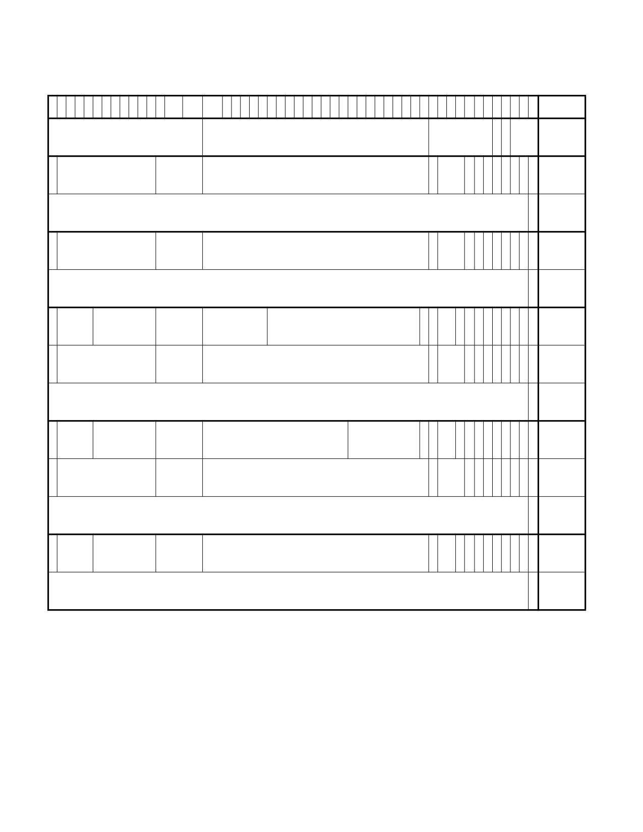
PAGING
6
6
6
6
5
5
5
5
5
5
5
5
5
3
3
3
2
2
2
2
2
2
2
2
2
2
1
1
1
1
1
1
1
1
1
1
M1
M-1
3
2
1
0
9
8
7
6
5
4
3
2
1
2
1
0
9
8
7
6
5
4
3
2
1
0
9
8
7
6
5
4
3
2
1
0
9
8
7
6
5
4
3
2
1
0
P
P
Address of PML4 table (4-level paging)
Reserved2
Ignored
C
W
Ign.
CR3
or PML5 table (5-level paging)
D
T
X
I
P
P
R
R
Rs
U
PML5E:
D
Ignored
Rsvd.
Address of PML4 table
4
Ign.
g
A
C
W
/
1
vd
/S
present
3
n
D
T
W
PML5E:
Ignored
0
not
present
I
P
P
R
X
Rs
U
PML4E:
Ignored
Rsvd.
Address of page-directory-pointer table
R
Ign.
g
A
C
W
/
1
D
vd
/S
present
n
D
T
W
PML4E:
Ignored
0
not
present
P
P
P
R
PDPTE:
X
Prot.
Address of
U
Ignored
Rsvd.
Reserved
A
R
Ign.
G
1
D
A
C
W
/
1
1GB
D
Key5
1GB page frame
/S
T
D
T
W
page
I
P
P
R
PDPTE:
X
U
Ignored
Rsvd.
Address of page directory
R
Ign.
0
g
A
C
W
/
1
page
D
/S
n
D
T
W
directory
PDPTE:
Ignored
0
not
present
P
P
P
R
PDE:
X
Prot.
Address of
U
Ignored
Rsvd.
Reserved
A
R
Ign.
G
1
D
A
C
W
/
1
2MB
D
Key
2MB page frame
/S
T
D
T
W
page
I
P
P
R
PDE:
X
U
Ignored
Rsvd.
Address of page table
R
Ign.
0
g
A
C
W
/
1
page
D
/S
n
D
T
W
table
PDE:
Ignored
0
not
present
P
P
P
R
PTE:
X
Prot.
U
Ignored
Rsvd.
Address of 4KB page frame
R
Ign.
G
A
D
A
C
W
/
1
4KB
D
Key
/S
T
D
T
W
page
PTE:
Ignored
0
not
present
Figure 5-11. Formats of CR3 and Paging-Structure Entries with 4-Level Paging and 5-Level Paging
NOTES:
1. If EPT is not enabled, M is an abbreviation for MAXPHYADDR. If EPT is enabled, M represents the value returned by
CPUID.80000008H:EAX[7:0]. See Section 5.1.4.
2. Reserved fields must be 0. On processors that support linear-address masking (see Section 4.4), bits 62:61 configure that feature and
may be set to 1. Because linear-address masking is not a paging feature, those bits are not illustrated here.
3. If IA32_EFER.NXE = 0 and the P flag of a paging-structure entry is 1, the XD flag (bit 63) is reserved.
4. Bit 11 is R (restart) only for HLAT paging; it is ignored for ordinary paging.
5. The protection key is used only if software has enabled the appropriate feature; see Section 5.6.2. It is ignored otherwise.
5-32
Vol. 3A
PAGING
5.5.5
Restart of HLAT Paging
As noted in Section 5.5.1, HLAT paging may specify that a translation of a linear address must be restarted. Specif-
ically, this occurs when HLAT paging encounters a paging-structure entry that sets bit 11 (see Section 5.5.4).
When this occurs, translation of the linear address is restarted using ordinary paging (starting with a paging struc-
ture identified using CR3). The restarted translation proceeds just as if the HLAT feature were not enabled. The
entire linear address is translated again, including those portions that had been used by HLAT paging prior to the
restart.
The process of restarting HLAT paging (using ordinary paging) always specifies a maximum page size to be used
when a resulting translation is cached in the TLBs. This maximum page size depends on the level of the paging-
structure entry that restarts the translation by setting bit 11; details are given in Section 5.5.4. The page size of
the translation produced by the restarted process is never greater than this maximum page size. See Section
5.10.2.2 for more discussion.
5.6
ACCESS RIGHTS
There is a translation for a linear address if the processes described in Section 5.3, Section 5.4.2, and Section 5.5
(depending upon the paging mode) completes and produces a physical address. Whether an access is permitted by
a translation is determined by the access rights specified by the paging-structure entries controlling the transla-
tion;1 paging-mode modifiers in CR0, CR4, and the IA32_EFER MSR; EFLAGS.AC; and the mode of the access.
Section 5.6.1 describes how the processor determines the access rights for each linear address. Section 5.6.2
provides additional information about how protection keys contribute to access-rights determination. (They do so
only with 4-level paging and 5-level paging, and only if CR4.PKE = 1 or CR4.PKS = 1.)
NOTE
If HLAT paging is restarted, permissions are determined only by the access rights specified by the
paging-structure entries that the subsequent ordinary paging used to translate the linear address.
The access rights specified by the entries used earlier by HLAT paging do not apply.
5.6.1
Determination of Access Rights
Every access to a linear address is either a supervisor-mode access or a user-mode access. For all instruction
fetches and most data accesses, this distinction is determined by the current privilege level (CPL): accesses made
while CPL < 3 are supervisor-mode accesses, while accesses made while CPL = 3 are user-mode accesses.
Some operations implicitly access system data structures with linear addresses; the resulting accesses to those
data structures are supervisor-mode accesses regardless of CPL. Examples of such accesses include the following:
accesses to the global descriptor table (GDT) or local descriptor table (LDT) to load a segment descriptor; accesses
to the interrupt descriptor table (IDT) when delivering an interrupt or exception; and accesses to the task-state
segment (TSS) as part of a task switch or change of CPL. All these accesses are called implicit supervisor-mode
accesses regardless of CPL. Other accesses made while CPL < 3 are called explicit supervisor-mode accesses.
Access rights are also controlled by the mode of a linear address as specified by the paging-structure entries
controlling the translation of the linear address. If the U/S flag (bit 2) is 0 in at least one of the paging-structure
entries, the address is a supervisor-mode address. Otherwise, the address is a user-mode address.
When the shadow-stack feature of control-flow enforcement technology (CET) is enabled, certain accesses to
linear addresses are considered shadow-stack accesses (see Section 18.2, “Shadow Stacks,” in the Intel® 64
and IA-32 Architectures Software Developer’s Manual, Volume 1). Like ordinary data accesses, each shadow-stack
access is defined as being either a user access or a supervisor access. In general, a shadow-stack access is a user
access if CPL = 3 and a supervisor access if CPL < 3. The WRUSS instruction is an exception; although it can be
executed only if CPL = 0, the processor treats its shadow-stack accesses as user accesses.
1. With PAE paging, the PDPTEs do not determine access rights.
Vol. 3A
5-33
PAGING
Shadow-stack accesses are allowed only to shadow-stack addresses. A linear address is a shadow-stack
address if the following are true of the translation of the linear address: (1) the R/W flag (bit 1) is 0 and the dirty
flag (bit 6) is 1 in the paging-structure entry that maps the page containing the linear address; and (2) the R/W
flag is 1 in every other paging-structure entry controlling the translation of the linear address.
The following items detail how paging determines access rights (only the items noted explicitly apply to shadow-
stack accesses):
NOTE
Many of the items below refer to an address with a protection key for which read (or write) access
is permitted. Section 5.6.2 provides details on when a protection key will permit (or not permit) a
data access (read or write) to a linear address using that protection key.
• For supervisor-mode accesses:
- Data may be read (implicitly or explicitly) from any supervisor-mode address with a protection key for
which read access is permitted.
- Data reads from user-mode pages.
Access rights depend on the value of CR4.SMAP:
• If CR4.SMAP = 0, data may be read from any user-mode address with a protection key for which read
access is permitted.
• If CR4.SMAP = 1, access rights depend on the value of EFLAGS.AC and whether the access is implicit or
explicit:
- If EFLAGS.AC = 1 and the access is explicit, data may be read from any user-mode address with a
protection key for which read access is permitted.
- If EFLAGS.AC = 0 or the access is implicit, data may not be read from any user-mode address.
- Data writes to supervisor-mode addresses.
Access rights depend on the value of CR0.WP:
• If CR0.WP = 0, data may be written to any supervisor-mode address with a protection key for which
write access is permitted.
• If CR0.WP = 1, data may be written to any supervisor-mode address with a translation for which the
R/W flag (bit 1) is 1 in every paging-structure entry controlling the translation and with a protection key
for which write access is permitted; data may not be written to any supervisor-mode address with a
translation for which the R/W flag is 0 in any paging-structure entry controlling the translation.
- Data writes to user-mode addresses.
Access rights depend on the value of CR0.WP:
• If CR0.WP = 0, access rights depend on the value of CR4.SMAP:
- If CR4.SMAP = 0, data may be written to any user-mode address with a protection key for which
write access is permitted.
- If CR4.SMAP = 1, access rights depend on the value of EFLAGS.AC and whether the access is
implicit or explicit:
• If EFLAGS.AC = 1 and the access is explicit, data may be written to any user-mode address
with a protection key for which write access is permitted.
• If EFLAGS.AC = 0 or the access is implicit, data may not be written to any user-mode address.
• If CR0.WP = 1, access rights depend on the value of CR4.SMAP:
- If CR4.SMAP = 0, data may be written to any user-mode address with a translation for which the
R/W flag is 1 in every paging-structure entry controlling the translation and with a protection key
for which write access is permitted; data may not be written to any user-mode address with a
translation for which the R/W flag is 0 in any paging-structure entry controlling the translation.
- If CR4.SMAP = 1, access rights depend on the value of EFLAGS.AC and whether the access is
implicit or explicit:
5-34
Vol. 3A
PAGING
• If EFLAGS.AC = 1 and the access is explicit, data may be written to any user-mode address
with a translation for which the R/W flag is 1 in every paging-structure entry controlling the
translation and with a protection key for which write access is permitted; data may not be
written to any user-mode address with a translation for which the R/W flag is 0 in any paging-
structure entry controlling the translation.
• If EFLAGS.AC = 0 or the access is implicit, data may not be written to any user-mode address.
- Instruction fetches from supervisor-mode addresses.
• For 32-bit paging or if IA32_EFER.NXE = 0, instructions may be fetched from any supervisor-mode
address.
• For other paging modes with IA32_EFER.NXE = 1, instructions may be fetched from any supervisor-
mode address with a translation for which the XD flag (bit 63) is 0 in every paging-structure entry
controlling the translation; instructions may not be fetched from any supervisor-mode address with a
translation for which the XD flag is 1 in any paging-structure entry controlling the translation.
- Instruction fetches from user-mode addresses.
Access rights depend on the values of CR4.SMEP:
• If CR4.SMEP = 0, access rights depend on the paging mode and the value of IA32_EFER.NXE:
- For 32-bit paging or if IA32_EFER.NXE = 0, instructions may be fetched from any user-mode
address.
- For other paging modes with IA32_EFER.NXE = 1, instructions may be fetched from any user-
mode address with a translation for which the XD flag is 0 in every paging-structure entry
controlling the translation; instructions may not be fetched from any user-mode address with a
translation for which the XD flag is 1 in any paging-structure entry controlling the translation.
• If CR4.SMEP = 1, instructions may not be fetched from any user-mode address.
- Supervisor-mode shadow-stack accesses are allowed only to supervisor-mode shadow-stack addresses
(see above).
• For user-mode accesses:
- Data reads.
Access rights depend on the mode of the linear address:
• Data may be read from any user-mode address with a protection key for which read access is
permitted.
• Data may not be read from any supervisor-mode address.
- Data writes.
Access rights depend on the mode of the linear address:
• Data may be written to any user-mode address with a translation for which the R/W flag is 1 in every
paging-structure entry controlling the translation and with a protection key for which write access is
permitted.
• Data may not be written to any supervisor-mode address.
- Instruction fetches.
Access rights depend on the mode of the linear address, the paging mode, and the value of
IA32_EFER.NXE:
• For 32-bit paging or if IA32_EFER.NXE = 0, instructions may be fetched from any user-mode address.
• For other paging modes with IA32_EFER.NXE = 1, instructions may be fetched from any user-mode
address with a translation for which the XD flag is 0 in every paging-structure entry controlling the
translation.
• Instructions may not be fetched from any supervisor-mode address.
- User-mode shadow-stack accesses made outside enclave mode are allowed only to user-mode shadow-
stack addresses (see above). User-mode shadow-stack accesses made in enclave mode are treated like
ordinary data accesses (see above).
Vol. 3A
5-35
PAGING
A processor may cache information from the paging-structure entries in TLBs and paging-structure caches (see
Section 5.10). These structures may include information about access rights. The processor may enforce access
rights based on the TLBs and paging-structure caches instead of on the paging structures in memory.
This fact implies that, if software modifies a paging-structure entry to change access rights, the processor might
not use that change for a subsequent access to an affected linear address (see Section 5.10.4.3). See Section
5.10.4.2 for how software can ensure that the processor uses the modified access rights.
5.6.2
Protection Keys
4-level paging and 5-level paging associate a 4-bit protection key with each linear address (the protection key
located in bits 62:59 of the paging-structure entry that mapped the page containing the linear address; see Section
5.5). Two protection key features control accesses to linear addresses based on their protection keys:
• If CR4.PKE = 1, the PKRU register determines, for each protection key, whether user-mode addresses with that
protection key may be read or written.
• If CR4.PKS = 1, the IA32_PKRS MSR (MSR index 6E1H) determines, for each protection key, whether
supervisor-mode addresses with that protection key may be read or written.
32-bit paging and PAE paging do not associate linear addresses with protection keys. For the purposes of Section
5.6.1, reads and writes are implicitly permitted for all protection keys with either of those paging modes.
The PKRU register (protection-key rights for user pages) is a 32-bit register with the following format: for each i
(0 ? i ? 15), PKRU[2i] is the access-disable bit for protection key i (ADi); PKRU[2i+1] is the write-disable bit for
protection key i (WDi). The IA32_PKRS MSR has the same format (bits 63:32 of the MSR are reserved and must be
zero).
Software can use the RDPKRU and WRPKRU instructions with ECX = 0 to read and write PKRU. In addition, the
PKRU register is XSAVE-managed state and can thus be read and written by instructions in the XSAVE feature set.
See Chapter 13, “Managing State Using the XSAVE Feature Set,” of Intel® 64 and IA-32 Architectures Software
Developer’s Manual, Volume 1, for more information about the XSAVE feature set.
Software can use the RDMSR and WRMSR instructions to read and write the IA32_PKRS MSR. Writes to the
IA32_PKRS MSR using WRMSR are not serializing. The IA32_PKRS MSR is not XSAVE-managed.
How a linear address’s protection key controls access to the address depends on the mode of the linear address:
• A linear address’s protection key controls only data accesses to the address. It does not in any way affect
instructions fetches from the address.
• If CR4.PKE = 0, the protection key of a user-mode address does not control data accesses to the address (for
the purposes of Section 5.6.1, reads and writes of user-mode addresses are implicitly permitted for all
protection keys).
If CR4.PKE = 1, use of the protection key i of a user-mode address depends on the value of the PKRU register:
- If ADi = 1, no data accesses are permitted.
- If WDi = 1, permission may be denied to certain data write accesses:
• User-mode write accesses are not permitted.
• Supervisor-mode write accesses are not permitted if CR0.WP = 1. (If CR0.WP = 0, WDi does not affect
supervisor-mode write accesses to user-mode addresses with protection key i.)
• If CR4.PKS = 0, the protection key of a supervisor-mode address does not control data accesses to the address
(for the purposes of Section 5.6.1, reads and writes of supervisor-mode addresses are implicitly permitted for
all protection keys).
If CR4.PKS = 1, use of the protection key i of a supervisor-mode address depends on the value of the
IA32_PKRS MSR:
- If ADi = 1, no data accesses are permitted.
- If WDi = 1, write accesses are not permitted if CR0.WP = 1. (If CR0.WP = 0, IA32_PKRS.WDi does not
affect write accesses to supervisor-mode addresses with protection key i.)
Protection keys apply to shadow-stack accesses just as they do to ordinary data accesses.
5-36
Vol. 3A
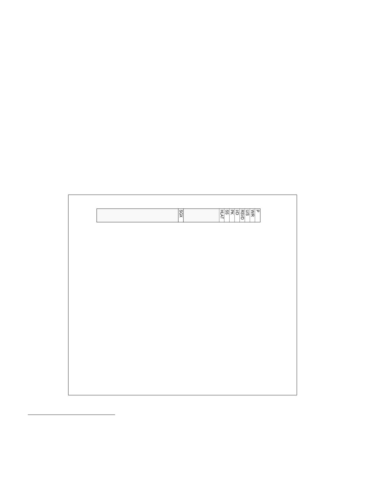
PAGING
5.7
PAGE-FAULT EXCEPTIONS
Accesses using linear addresses may cause page-fault exceptions (#PF; exception 14). An access to a linear
address may cause a page-fault exception for either of two reasons: (1) there is no translation for the linear
address; or (2) there is a translation for the linear address, but its access rights do not permit the access.
As noted in Section 5.3, Section 5.4.2, and Section 5.5, there is no translation for a linear address if the translation
process for that address would use a paging-structure entry in which the P flag (bit 0) is 0 or one that sets a
reserved bit.1 If there is a translation for a linear address, its access rights are determined as specified in Section
5.6.
When Intel® Software Guard Extensions (Intel® SGX) are enabled, the processor may deliver exception 14 for
reasons unrelated to paging. See Section 38.3, “Access-control Requirements,” and Section 38.20, “Enclave Page
Cache Map (EPCM),” in Chapter 38, “Enclave Access Control and Data Structures.” Such an exception is called an
SGX-induced page fault. The processor uses the error code to distinguish SGX-induced page faults from ordinary
page faults.
When a page fault occurs, the processor loads the CR2 register with the linear address that generated the excep-
tion. If linear-address masking had been in effect (Section 4.4), the address recorded reflects the result of that
masking and does not contain any masked metadata. If the page-fault exception occurred during execution of an
instruction in enclave mode (and not during delivery of an event incident to enclave mode), bits 11:0 of the address
are cleared.
Figure 5-12 illustrates the error code that the processor provides on delivery of a page-fault exception. The
following items explain how the bits in the error code describe the nature of the page-fault exception:
31
15
7
6
5
4
3
2
1
0
Reserved
Reserved
P
0
The fault was caused by a non-present page.
1
The fault was caused by a page-level protection violation.
W/R
0
The access causing the fault was a read.
1
The access causing the fault was a write.
U/S
0
A supervisor-mode access caused the fault.
1
A user-mode access caused the fault.
RSVD
0
The fault was not caused by reserved bit violation.
The fault was caused by a reserved bit set to 1 in some
1
paging-structure entry.
I/D
0 The fault was not caused by an instruction fetch.
1 The fault was caused by an instruction fetch.
PK
0 The fault was not caused by protection keys.
1 There was a protection-key violation.
SS
0 The fault was not caused by a shadow-stack access.
1 The fault was caused by a shadow-stack access.
HLAT
0 The fault occurred during ordinary paging or due to access rights.
1 The fault occurred during HLAT paging.
SGX
0 The fault is not related to SGX.
1 The fault resulted from violation of SGX-specific access-control
requirements.
Figure 5-12. Page-Fault Error Code
1. If HLAT paging encounters a paging-structure entry that sets a reserved bit, there is no translation even if the bit 11 of the entry
indicates a restart. In this case, there is a page fault and the translation is not restarted.
Vol. 3A
5-37
PAGING
•
P flag (bit 0).
This flag is 0 if there is no translation for the linear address because the P flag was 0 in one of the paging-
structure entries used to translate that address.
•
W/R (bit 1).
If the access causing the page-fault exception was a write, this flag is 1; otherwise, it is 0. This flag describes
the access causing the page-fault exception, not the access rights specified by paging.
•
U/S (bit 2).
If a user-mode access caused the page-fault exception, this flag is 1; it is 0 if a supervisor-mode access did so.
This flag describes the access causing the page-fault exception, not the access rights specified by paging. User-
mode and supervisor-mode accesses are defined in Section 5.6.
•
RSVD flag (bit 3).
This flag is 1 if there is no translation for the linear address because a reserved bit was set in one of the paging-
structure entries used to translate that address. (Because reserved bits are not checked in a paging-structure
entry whose P flag is 0, bit 3 of the error code can be set only if bit 0 is also set.1)
Bits reserved in the paging-structure entries are reserved for future functionality. Software developers should
be aware that such bits may be used in the future and that a paging-structure entry that causes a page-fault
exception on one processor might not do so in the future.
•
I/D flag (bit 4).
This flag is 1 if (1) the access causing the page-fault exception was an instruction fetch; and (2) either
(a) CR4.SMEP = 1; or (b) both (i) CR4.PAE = 1 (either PAE paging, 4-level paging, or 5-level paging is in use);
and (ii) IA32_EFER.NXE = 1. Otherwise, the flag is 0. This flag describes the access causing the page-fault
exception, not the access rights specified by paging.
•
PK flag (bit 5).
This flag is 1 only for data accesses and only with 4-level paging and 5-level paging. In these cases, the setting
depends on the mode of the address being accessed:
- For accesses to supervisor-mode addresses, the flag is set if (1) CR4.PKS = 1; (2) the linear address has
protection key i; and (3) the IA32_PKRS MSR (see Section 5.6.2) is such that either (a) ADi = 1; or (b) the
following all hold: (i) WDi = 1; (ii) the access is a write access; and (iii) either CR0.WP = 1 or the access
causing the page-fault exception was a user-mode access. (Note that this flag may be set on page faults
due to user-mode accesses to supervisor-mode addresses.)
- For accesses to user-mode addresses, the flag is set if (1) CR4.PKE = 1; (2) the linear address has
protection key i; and (3) the PKRU register (see Section 5.6.2) is such that either (a) ADi = 1; or (b) the
following all hold: (i) WDi = 1; (ii) the access is a write access; and (iii) either CR0.WP = 1 or the access
causing the page-fault exception was a user-mode access.
•
SS (bit 6).
If the access causing the page-fault exception was a shadow-stack access (including shadow-stack accesses in
enclave mode), this flag is 1; otherwise, it is 0. This flag describes the access causing the page-fault exception,
not the access rights specified by paging.
•
HLAT (bit 7).
This flag is 1 if there is no translation for the linear address using HLAT paging because, in one of the paging-
structure entries used to translate that address, either the P flag was 0 or a reserved bit was set. An error code
will set this flag only if it clears bit 0 or sets bit 3. This flag will not be set by a page fault resulting from a
violation of access rights, nor for one encountered during ordinary paging, including the case in which there has
been a restart of HLAT paging.
•
SGX flag (bit 15).
This flag is 1 if the exception is unrelated to paging and resulted from violation of SGX-specific access-control
requirements. Because such a violation can occur only if there is no ordinary page fault, this flag is set only if
the P flag (bit 0) is 1 and the RSVD flag (bit 3) and the PK flag (bit 5) are both 0.
Page-fault exceptions occur only due to an attempt to use a linear address. Failures to load the PDPTE registers
with PAE paging (see Section 5.4.1) cause general-protection exceptions (#GP(0)) and not page-fault exceptions.
1. Some past processors had errata for some page faults that occur when there is no translation for the linear address because the P
flag was 0 in one of the paging-structure entries used to translate that address. Due to these errata, some such page faults pro-
duced error codes that cleared bit 0 (P flag) and set bit 3 (RSVD flag).
5-38
Vol. 3A
PAGING
5.8
ACCESSED AND DIRTY FLAGS
For any paging-structure entry that is used during linear-address translation, bit 5 is the accessed flag.1 For
paging-structure entries that map a page (as opposed to referencing another paging structure), bit 6 is the dirty
flag. These flags are provided for use by memory-management software to manage the transfer of pages and
paging structures into and out of physical memory.
Whenever the processor uses a paging-structure entry as part of linear-address translation, it sets the accessed
flag in that entry (if it is not already set).
Whenever there is a write to a linear address, the processor sets the dirty flag (if it is not already set) in the paging-
structure entry that identifies the final physical address for the linear address (either a PTE or a paging-structure
entry in which the PS flag is 1).
The previous two paragraphs apply also to HLAT paging. If HLAT paging encounters a paging-structure entry that
sets bit 11, indicating a restart, the processor will set the accessed flag in that entry; it will not set the dirty flag
because, if an entry indicates a restart, it does identify the final physical address for the linear address being trans-
lated.
NOTE
If software on one logical processor writes to a page while software on another logical processor
concurrently clears the R/W flag in the paging-structure entry that maps the page, execution on
some processors may result in the entry’s dirty flag being set (due to the write on the first logical
processor) and the entry’s R/W flag being clear (due to the update to the entry on the second
logical processor). This will never occur on a processor that supports control-flow enforcement
technology (CET). Specifically, a processor that supports CET will never set the dirty flag in a
paging-structure entry in which the R/W flag is clear.
Memory-management software may clear these flags when a page or a paging structure is initially loaded into
physical memory. These flags are “sticky,” meaning that, once set, the processor does not clear them; only soft-
ware can clear them.
A processor may cache information from the paging-structure entries in TLBs and paging-structure caches (see
Section 5.10). This fact implies that, if software changes an accessed flag or a dirty flag from 1 to 0, the processor
might not set the corresponding bit in memory on a subsequent access using an affected linear address (see
Section 5.10.4.3). See Section 5.10.4.2 for how software can ensure that these bits are updated as desired.
NOTE
The accesses used by the processor to set these flags may or may not be exposed to the
processor’s self-modifying code detection logic. If the processor is executing code from the same
memory area that is being used for the paging structures, the setting of these flags may or may not
result in an immediate change to the executing code stream.
5.9
PAGING AND MEMORY TYPING
The memory type of a memory access refers to the type of caching used for that access. Chapter 14, “Memory
Cache Control‚” provides many details regarding memory typing in the Intel-64 and IA-32 architectures. This
section describes how paging contributes to the determination of memory typing.
The way in which paging contributes to memory typing depends on whether the processor supports the Page
Attribute Table (PAT; see Section 14.12).2 Section 5.9.1 and Section 5.9.2 explain how paging contributes to
memory typing depending on whether the PAT is supported.
1. With PAE paging, the PDPTEs are not used during linear-address translation but only to load the PDPTE registers for some execu-
tions of the MOV CR instruction (see Section 5.4.1). For this reason, the PDPTEs do not contain accessed flags with PAE paging.
2. The PAT is supported on Pentium III and more recent processor families. See Section 5.1.4 for how to determine whether the PAT is
supported.
Vol. 3A
5-39
PAGING
5.9.1
Paging and Memory Typing When the PAT is Not Supported (Pentium Pro and Pentium
II Processors)
NOTE
The PAT is supported on all processors that support 4-level paging or 5-level paging. Thus, this
section applies only to 32-bit paging and PAE paging.
If the PAT is not supported, paging contributes to memory typing in conjunction with the memory-type range regis-
ters (MTRRs) as specified in Table 14-6 in Section 14.5.2.1.
For any access to a physical address, the table combines the memory type specified for that physical address by
the MTRRs with a PCD value and a PWT value. The latter two values are determined as follows:
• For an access to a PDE with 32-bit paging, the PCD and PWT values come from CR3.
• For an access to a PDE with PAE paging, the PCD and PWT values come from the relevant PDPTE register.
• For an access to a PTE, the PCD and PWT values come from the relevant PDE.
• For an access to the physical address that is the translation of a linear address, the PCD and PWT values come
from the relevant PTE (if the translation uses a 4-KByte page) or the relevant PDE (otherwise).
• With PAE paging, the UC memory type is used when loading the PDPTEs (see Section 5.4.1).
5.9.2
Paging and Memory Typing When the PAT is Supported (Pentium III and More Recent
Processor Families)
If the PAT is supported, paging contributes to memory typing in conjunction with the PAT and the memory-type
range registers (MTRRs) as specified in Table 14-7 in Section 14.5.2.2.
The PAT is a 64-bit MSR (IA32_PAT; MSR index 277H) comprising eight (8) 8-bit entries (entry i comprises
bits 8i+7:8i of the MSR).
For any access to a physical address, the table combines the memory type specified for that physical address by
the MTRRs with a memory type selected from the PAT. Table 14-11 in Section 14.12.3 specifies how a memory type
is selected from the PAT. Specifically, it comes from entry i of the PAT, where i is defined as follows:
• For an access to an entry in a paging structure whose address is in CR3 (e.g., the PML4 table with 4-level
paging):
- For 4-level paging or 5-level paging with CR4.PCIDE = 1, i = 0.
- Otherwise, i = 2*PCD+PWT, where the PCD and PWT values come from CR3.
• For an access to a PDE with PAE paging, i = 2*PCD+PWT, where the PCD and PWT values come from the
relevant PDPTE register.
• For an access to a paging-structure entry X whose address is in another paging-structure entry Y, i =
2*PCD+PWT, where the PCD and PWT values come from Y.
• For an access to the physical address that is the translation of a linear address, i = 4*PAT+2*PCD+PWT, where
the PAT, PCD, and PWT values come from the relevant PTE (if the translation uses a 4-KByte page), the relevant
PDE (if the translation uses a 2-MByte page or a 4-MByte page), or the relevant PDPTE (if the translation uses
a 1-GByte page).
• With PAE paging, the WB memory type is used when loading the PDPTEs (see Section 5.4.1).1
1. Some older IA-32 processors used the UC memory type when loading the PDPTEs. Some processors may use the UC memory type if
CR0.CD = 1 or if the MTRRs are disabled. These behaviors are model-specific and not architectural.
5-40
Vol. 3A
PAGING
5.9.3
Caching Paging-Related Information about Memory Typing
A processor may cache information from the paging-structure entries in TLBs and paging-structure caches (see
Section 5.10). These structures may include information about memory typing. The processor may use memory-
typing information from the TLBs and paging-structure caches instead of from the paging structures in memory.
This fact implies that, if software modifies a paging-structure entry to change the memory-typing bits, the
processor might not use that change for a subsequent translation using that entry or for access to an affected
linear address. See Section 5.10.4.2 for how software can ensure that the processor uses the modified memory
typing.
5.10
CACHING TRANSLATION INFORMATION
The Intel-64 and IA-32 architectures may accelerate the address-translation process by caching data from the
paging structures on the processor. Because the processor does not ensure that the data that it caches are always
consistent with the structures in memory, it is important for software developers to understand how and when the
processor may cache such data. They should also understand what actions software can take to remove cached
data that may be inconsistent and when it should do so. This section provides software developers information
about the relevant processor operation.
Section 5.10.1 introduces process-context identifiers (PCIDs), which a logical processor may use to distinguish
information cached for different linear-address spaces. Section 5.10.2 and Section 5.10.3 describe how the
processor may cache information in translation lookaside buffers (TLBs) and paging-structure caches, respectively.
Section 5.10.4 explains how software can remove inconsistent cached information by invalidating portions of the
TLBs and paging-structure caches. Section 5.10.5 describes special considerations for multiprocessor systems.
5.10.1 Process-Context Identifiers (PCIDs)
Process-context identifiers (PCIDs) are a facility by which a logical processor may cache information for multiple
linear-address spaces. The processor may retain cached information when software switches to a different linear-
address space with a different PCID (e.g., by loading CR3; see Section 5.10.4.1 for details).
A PCID is a 12-bit identifier. Non-zero PCIDs are enabled by setting the PCIDE flag (bit 17) of CR4. If CR4.PCIDE =
0, the current PCID is always 000H; otherwise, the current PCID is the value of bits 11:0 of CR3.1 Not all proces-
sors allow CR4.PCIDE to be set to 1; see Section 5.1.4 for how to determine whether this is allowed.
The processor ensures that CR4.PCIDE can be 1 only in IA-32e mode (thus, 32-bit paging and PAE paging use only
PCID 000H). In addition, software can change CR4.PCIDE from 0 to 1 only if CR3[11:0] = 000H. These require-
ments are enforced by the following limitations on the MOV CR instruction:
• MOV to CR4 causes a general-protection exception (#GP) if it would change CR4.PCIDE from 0 to 1 and either
IA32_EFER.LMA = 0 or CR3[11:0] ≠ 000H.
• MOV to CR0 causes a general-protection exception if it would clear CR0.PG to 0 while CR4.PCIDE = 1.
When a logical processor creates entries in the TLBs (Section 5.10.2) and paging-structure caches (Section
5.10.3), it associates those entries with the current PCID. When using entries in the TLBs and paging-structure
caches to translate a linear address, a logical processor uses only those entries associated with the current PCID
(see Section 5.10.2.4 for an exception).
If CR4.PCIDE = 0, a logical processor does not cache information for any PCID other than 000H. This is because
(1) if CR4.PCIDE = 0, the logical processor will associate any newly cached information with the current PCID,
000H; and (2) if MOV to CR4 clears CR4.PCIDE, all cached information is invalidated (see Section 5.10.4.1).
1. Note that, while HLAT paging (Section 5.5.3) does not use CR3 to locate the first paging structure, it does use the PCID in CR3[11:0]
when CR4.PCIDE = 1.
Vol. 3A
5-41
PAGING
NOTE
In revisions of this manual that were produced when no processors allowed CR4.PCIDE to be set to
1, Section 5.10, “Caching Translation Information,” discussed the caching of translation information
without any reference to PCIDs. While the section now refers to PCIDs in its specification of this
caching, this documentation change is not intended to imply any change to the behavior of
processors that do not allow CR4.PCIDE to be set to 1.
5.10.2 Translation Lookaside Buffers (TLBs)
A processor may cache information about the translation of linear addresses in translation lookaside buffers (TLBs).
In general, TLBs contain entries that map page numbers to page frames; these terms are defined in Section
5.10.2.1. Section 5.10.2.2 describes how information may be cached in TLBs, and Section 5.10.2.3 gives details of
TLB usage. Section 5.10.2.4 explains the global-page feature, which allows software to indicate that certain trans-
lations should receive special treatment when cached in the TLBs.
5.10.2.1 Page Numbers, Page Frames, and Page Offsets
Section 5.3, Section 5.4.2, and Section 5.5 give details of how the different paging modes translate linear
addresses to physical addresses. Specifically, the upper bits of a linear address (called the page number) deter-
mine the upper bits of the physical address (called the page frame); the lower bits of the linear address (called the
page offset) determine the lower bits of the physical address. The boundary between the page number and the
page offset is determined by the page size. Specifically:
•
32-bit paging:
- If the translation does not use a PTE (because CR4.PSE = 1 and the PS flag is 1 in the PDE used), the page
size is 4 MBytes and the page number comprises bits 31:22 of the linear address.
- If the translation does use a PTE, the page size is 4 KBytes and the page number comprises bits 31:12 of
the linear address.
• PAE paging:
- If the translation does not use a PTE (because the PS flag is 1 in the PDE used), the page size is 2 MBytes
and the page number comprises bits 31:21 of the linear address.
- If the translation does use a PTE, the page size is 4 KBytes and the page number comprises bits 31:12 of
the linear address.
•
4-level paging and 5-level paging:
- If the translation does not use a PDE (because the PS flag is 1 in the PDPTE used), the page size is 1 GByte
and the page number comprises bits 47:30 of the linear address.
- If the translation does use a PDE but does not uses a PTE (because the PS flag is 1 in the PDE used), the
page size is 2 MBytes and the page number comprises bits 47:21 of the linear address.
- If the translation does use a PTE, the page size is 4 KBytes and the page number comprises bits 47:12 of
the linear address.
- The page size identified by the preceding items may be reduced if there has been a restart of HLAT paging
(see Section 5.5.5). Restart of HLAT paging always specifies a maximum page size; this page size is
determined by the level of the paging-structure entry that caused the restart. The page size used by the
translation is the minimum of the maximum page size specified by the restart and the page size determined
by the restarted translation (as specified by the previous items).
For example, suppose that HLAT paging encounters a PDE that sets bit 11, indicating a restart. As a result,
the restart uses a maximum page size of 2 MBytes. Suppose that the restarted translation encounters a
PDPTE that sets bit 7, indicating a 1-GByte page. In this case, the translation produced will have a page size
of 2 MBytes (the smaller of the two sizes).
5-42
Vol. 3A
PAGING
5.10.2.2 Caching Translations in TLBs
The processor may accelerate the paging process by caching individual translations in translation lookaside
buffers (TLBs). Each entry in a TLB is an individual translation. Each translation is referenced by a page number.
It contains the following information from the paging-structure entries used to translate linear addresses with the
page number:
• The physical address corresponding to the page number (the page frame).
• The access rights from the paging-structure entries used to translate linear addresses with the page number
(see Section 5.6):
- The logical-AND of the R/W flags.
- The logical-AND of the U/S flags.
- The logical-OR of the XD flags (necessary only if IA32_EFER.NXE = 1).
- The protection key (only with 4-level paging and 5-level paging).
• Attributes from a paging-structure entry that identifies the final page frame for the page number (either a PTE
or a paging-structure entry in which the PS flag is 1):
- The dirty flag (see Section 5.8).
- The memory type (see Section 5.9).
(TLB entries may contain other information as well. A processor may implement multiple TLBs, and some of these
may be for special purposes, e.g., only for instruction fetches. Such special-purpose TLBs may not contain some of
this information if it is not necessary. For example, a TLB used only for instruction fetches need not contain infor-
mation about the R/W and dirty flags.)
As noted in Section 5.10.1, any TLB entries created by a logical processor are associated with the current PCID.
Processors need not implement any TLBs. Processors that do implement TLBs may invalidate any TLB entry at any
time. Software should not rely on the existence of TLBs or on the retention of TLB entries.
5.10.2.3 Details of TLB Use
Because the TLBs cache entries only for linear addresses with translations, there can be a TLB entry for a page
number only if the P flag is 1 and the reserved bits are 0 in each of the paging-structure entries used to translate
that page number. In addition, the processor does not cache a translation for a page number unless the accessed
flag is 1 in each of the paging-structure entries used during translation; before caching a translation, the processor
sets any of these accessed flags that is not already 1.
Subject to the limitations given in the previous paragraph, the processor may cache a translation for any linear
address, even if that address is not used to access memory. For example, the processor may cache translations
required for prefetches and for accesses that result from speculative execution that would never actually occur in
the executed code path.
If the page number of a linear address corresponds to a TLB entry associated with the current PCID, the processor
may use that TLB entry to determine the page frame, access rights, and other attributes for accesses to that linear
address. In this case, the processor may not actually consult the paging structures in memory. The processor may
retain a TLB entry unmodified even if software subsequently modifies the relevant paging-structure entries in
memory. See Section 5.10.4.2 for how software can ensure that the processor uses the modified paging-structure
entries.
If the paging structures specify a translation using a page larger than 4 KBytes, some processors may cache
multiple smaller-page TLB entries for that translation. Each such TLB entry would be associated with a page
number corresponding to the smaller page size (e.g., bits 47:12 of a linear address with 4-level paging), even
though part of that page number (e.g., bits 20:12) is part of the offset with respect to the page specified by the
paging structures. The upper bits of the physical address in such a TLB entry are derived from the physical address
in the PDE used to create the translation, while the lower bits come from the linear address of the access for which
the translation is created. There is no way for software to be aware that multiple translations for smaller pages
have been used for a large page. For example, an execution of INVLPG for a linear address on such a page invali-
dates any and all smaller-page TLB entries for the translation of any linear address on that page.
Vol. 3A
5-43
PAGING
If software modifies the paging structures so that the page size used for a 4-KByte range of linear addresses
changes, the TLBs may subsequently contain multiple translations for the address range (one for each page size).
A reference to a linear address in the address range may use any of these translations. Which translation is used
may vary from one execution to another, and the choice may be implementation-specific.
5.10.2.4 Global Pages
The Intel-64 and IA-32 architectures also allow for global pages when the PGE flag (bit 7) is 1 in CR4. If the G flag
(bit 8) is 1 in a paging-structure entry that maps a page (either a PTE or a paging-structure entry in which the PS
flag is 1), any TLB entry cached for a linear address using that paging-structure entry is considered to be global.
Because the G flag is used only in paging-structure entries that map a page, and because information from such
entries is not cached in the paging-structure caches, the global-page feature does not affect the behavior of the
paging-structure caches.
A logical processor may use a global TLB entry to translate a linear address, even if the TLB entry is associated with
a PCID different from the current PCID.
5.10.3 Paging-Structure Caches
In addition to the TLBs, a processor may cache other information about the paging structures in memory.
5.10.3.1 Caches for Paging Structures
A processor may support any or all of the following paging-structure caches:
• PML5E cache (5-level paging only). Each PML5E-cache entry is referenced by a 9-bit value and is used for
linear addresses for which bits 56:48 have that value. The entry contains information from the PML5E used to
translate such linear addresses:
- The physical address from the PML5E (the address of the PML4 table).
- The value of the R/W flag of the PML5E.
- The value of the U/S flag of the PML5E.
- The value of the XD flag of the PML5E.
- The values of the PCD and PWT flags of the PML5E.
The following items detail how a processor may use the PML5E cache:
- If the processor has a PML5E-cache entry for a linear address, it may use that entry when translating the
linear address (instead of the PML5E in memory).
- The processor does not create a PML5E-cache entry unless the P flag is 1 and all reserved bits are 0 in the
PML5E in memory.
- The processor does not create a PML5E-cache entry unless the accessed flag is 1 in the PML5E in memory;
before caching a translation, the processor sets the accessed flag if it is not already 1.
- The processor may create a PML5E-cache entry even if there are no translations for any linear address that
might use that entry (e.g., because the P flags are 0 in all entries in the referenced PML4 table).
- If the processor creates a PML5E-cache entry, the processor may retain it unmodified even if software
subsequently modifies the corresponding PML5E in memory.
• PML4E cache (4-level paging and 5-level paging only). The use of the PML4E cache depends on the paging
mode:
- For 4-level paging, each PML4E-cache entry is referenced by a 9-bit value and is used for linear addresses
for which bits 47:39 have that value.
- For 5-level paging, each PML4E-cache entry is referenced by an 18-bit value and is used for linear
addresses for which bits 56:39 have that value.
A PML4E-cache entry contains information from the PML5E and PML4E used to translate the relevant linear
addresses (for 4-level paging, the PML5E does not apply):
5-44
Vol. 3A
PAGING
- The physical address from the PML4E (the address of the page-directory-pointer table).
- The logical-AND of the R/W flags in the PML5E and the PML4E.
- The logical-AND of the U/S flags in the PML5E and the PML4E.
- The logical-OR of the XD flags in the PML5E and the PML4E.
- The values of the PCD and PWT flags of the PML4E.
The following items detail how a processor may use the PML4E cache:
- If the processor has a PML4E-cache entry for a linear address, it may use that entry when translating the
linear address (instead of the PML5E and PML4E in memory).
- The processor does not create a PML4E-cache entry unless the P flags are 1 and all reserved bits are 0 in
the PML5E and the PML4E in memory.
- The processor does not create a PML4E-cache entry unless the accessed flags are 1 in the PML5E and the
PML4E in memory; before caching a translation, the processor sets any accessed flags that are not already
1.
- The processor may create a PML4E-cache entry even if there are no translations for any linear address that
might use that entry (e.g., because the P flags are 0 in all entries in the referenced page-directory-pointer
table).
- If the processor creates a PML4E-cache entry, the processor may retain it unmodified even if software
subsequently modifies the corresponding PML4E in memory.
•
PDPTE cache (4-level paging and 5-level paging only).1 The use of the PML4E cache depends on the paging
mode:
- For 4-level paging, each PDPTE-cache entry is referenced by an 18-bit value and is used for linear
addresses for which bits 47:30 have that value.
- For 5-level paging, each PDPTE-cache entry is referenced by a 27-bit value and is used for linear addresses
for which bits 56:30 have that value.
A PDPTE-cache entry contains information from the PML5E, PML4E, PDPTE used to translate the relevant linear
addresses (for 4-level paging, the PML5E does not apply):
- The physical address from the PDPTE (the address of the page directory). (No PDPTE-cache entry is created
for a PDPTE that maps a 1-GByte page.)
- The logical-AND of the R/W flags in the PML5E, PML4E, and PDPTE.
- The logical-AND of the U/S flags in the PML5E, PML4E, and PDPTE.
- The logical-OR of the XD flags in the PML5E, PML4E, and PDPTE.
- The values of the PCD and PWT flags of the PDPTE.
The following items detail how a processor may use the PDPTE cache:
- If the processor has a PDPTE-cache entry for a linear address, it may use that entry when translating the
linear address (instead of the PML5E, PML4E, and PDPTE in memory).
- The processor does not create a PDPTE-cache entry unless the P flags are 1, the PS flags are 0, and the
reserved bits are 0 in the PML5E, PML4E, and PDPTE in memory.
- The processor does not create a PDPTE-cache entry unless the accessed flags are 1 in the PML5E, PML4E,
and PDPTE in memory; before caching a translation, the processor sets any accessed flags that are not
already 1.
- The processor may create a PDPTE-cache entry even if there are no translations for any linear address that
might use that entry.
- If the processor creates a PDPTE-cache entry, the processor may retain it unmodified even if software
subsequently modifies the corresponding PML5E, PML4E, or PDPTE in memory.
1.
With PAE paging, the PDPTEs are stored in internal, non-architectural registers. The operation of these registers is described in Sec-
tion 5.4.1 and differs from that described here.
Vol. 3A
5-45
PAGING
• PDE cache. The use of the PDE cache depends on the paging mode:
- For 32-bit paging, each PDE-cache entry is referenced by a 10-bit value and is used for linear addresses for
which bits 31:22 have that value.
- For PAE paging, each PDE-cache entry is referenced by an 11-bit value and is used for linear addresses for
which bits 31:21 have that value.
- For 4-level paging, each PDE-cache entry is referenced by a 27-bit value and is used for linear addresses for
which bits 47:21 have that value.
- For 5-level paging, each PDE-cache entry is referenced by a 36-bit value and is used for linear addresses for
which bits 56:21 have that value.
A PDE-cache entry contains information from the PML5E, PML4E, PDPTE, and PDE used to translate the relevant
linear addresses (for 32-bit paging and PAE paging, only the PDE applies; for 4-level paging, the PML5E does
not apply):
- The physical address from the PDE (the address of the page table). (No PDE-cache entry is created for a
PDE that maps a page.)
- The logical-AND of the R/W flags in the PML5E, PML4E, PDPTE, and PDE.
- The logical-AND of the U/S flags in the PML5E, PML4E, PDPTE, and PDE.
- The logical-OR of the XD flags in the PML5E, PML4E, PDPTE, and PDE.
- The values of the PCD and PWT flags of the PDE.
The following items detail how a processor may use the PDE cache (references below to PML5Es, PML4Es, and
PDPTEs apply only to 4-level paging and to 5-level paging, as appropriate):
- If the processor has a PDE-cache entry for a linear address, it may use that entry when translating the
linear address (instead of the PML5E, PML4E, PDPTE, and PDE in memory).
- The processor does not create a PDE-cache entry unless the P flags are 1, the PS flags are 0, and the
reserved bits are 0 in the PML5E, PML4E, PDPTE, and PDE in memory.
- The processor does not create a PDE-cache entry unless the accessed flag is 1 in the PML5E, PML4E, PDPTE,
and PDE in memory; before caching a translation, the processor sets any accessed flags that are not
already 1.
- The processor may create a PDE-cache entry even if there are no translations for any linear address that
might use that entry.
- If the processor creates a PDE-cache entry, the processor may retain it unmodified even if software subse-
quently modifies the corresponding PML5E, PML4E, PDPTE, or PDE in memory.
Information from a paging-structure entry can be included in entries in the paging-structure caches for other
paging-structure entries referenced by the original entry. For example, if the R/W flag is 0 in a PML4E, then the R/W
flag will be 0 in any PDPTE-cache entry for a PDPTE from the page-directory-pointer table referenced by that
PML4E. This is because the R/W flag of each such PDPTE-cache entry is the logical-AND of the R/W flags in the
appropriate PML4E and PDPTE.
On processors that support HLAT paging (see Section 5.5.1), each entry in a paging-structure cache indicates
whether the entry was cached during ordinary paging or HLAT paging. When the processor commences linear-
address translation using ordinary paging (respectively, HLAT paging), it will use only entries that indicate that they
were cached during ordinary paging (respectively, HLAT paging).
Entries that were cached during HLAT paging also include the restart flag (bit 11) of the original paging-structure
entry. When the processor commences HLAT paging using such an entry, it immediately restarts (using ordinary
paging) if this cached restart flag is 1.
The paging-structure caches contain information only from paging-structure entries that reference other paging
structures (and not those that map pages). Because the G flag is not used in such paging-structure entries, the
global-page feature does not affect the behavior of the paging-structure caches.
The processor may create entries in paging-structure caches for translations required for prefetches and for
accesses that are a result of speculative execution that would never actually occur in the executed code path.
5-46
Vol. 3A
PAGING
As noted in Section 5.10.1, any entries created in paging-structure caches by a logical processor are associated
with the current PCID.
A processor may or may not implement any of the paging-structure caches. Software should rely on neither their
presence nor their absence. The processor may invalidate entries in these caches at any time. Because the
processor may create the cache entries at the time of translation and not update them following subsequent modi-
fications to the paging structures in memory, software should take care to invalidate the cache entries appropri-
ately when causing such modifications. The invalidation of TLBs and the paging-structure caches is described in
Section 5.10.4.
5.10.3.2 Using the Paging-Structure Caches to Translate Linear Addresses
When a linear address is accessed, the processor uses a procedure such as the following to determine the physical
address to which it translates and whether the access should be allowed:
• If the processor finds a TLB entry that is for the page number of the linear address and that is associated with
the current PCID (or which is global), it may use the physical address, access rights, and other attributes from
that entry.
• If the processor does not find a relevant TLB entry, it may use the upper bits of the linear address to select an
entry from the PDE cache that is associated with the current PCID (Section 5.10.3.1 indicates which bits are
used in each paging mode). It can then use that entry to complete the translation process (locating a PTE, etc.)
as if it had traversed the PDE (and, for 4-level paging and 5-level paging, the PDPTE, PML4E, and PML5E, as
appropriate) corresponding to the PDE-cache entry.
• The following items apply when 4-level paging or 5-level paging is used:
- If the processor does not find a relevant TLB entry or PDE-cache entry, it may use the upper bits of the
linear address (for 4-level paging, bits 47:30; for 5-level paging, bits 56:30) to select an entry from the
PDPTE cache that is associated with the current PCID. It can then use that entry to complete the translation
process (locating a PDE, etc.) as if it had traversed the PDPTE, the PML4E, and (for 5-level paging) the
PML5E corresponding to the PDPTE-cache entry.
- If the processor does not find a relevant TLB entry, PDE-cache entry, or PDPTE-cache entry, it may use the
upper bits of the linear address (for 4-level paging, bits 47:39; for 5-level paging, bits 56:39) to select an
entry from the PML4E cache that is associated with the current PCID. It can then use that entry to complete
the translation process (locating a PDPTE, etc.) as if it had traversed the corresponding PML4E.
- With 5-level paging, if the processor does not find a relevant TLB entry, PDE-cache entry, PDPTE-cache
entry, or PML4E-cache entry, it may use bits 56:48 of the linear address to select an entry from the PML5E
cache that is associated with the current PCID. It can then use that entry to complete the translation
process (locating a PML4E, etc.) as if it had traversed the corresponding PML5E.
(Any of the above steps would be skipped if the processor does not support the cache in question.)
If the processor does not find a TLB or paging-structure-cache entry for the linear address, it uses the linear
address to traverse the entire paging-structure hierarchy, as described in Section 5.3, Section 5.4.2, and Section
5.5.
5.10.3.3 Multiple Cached Entries for a Single Paging-Structure Entry
The paging-structure caches and TLBs may contain multiple entries associated with a single PCID and with infor-
mation derived from a single paging-structure entry. The following items give some examples for 4-level paging:
• Suppose that two PML4Es contain the same physical address and thus reference the same page-directory-
pointer table. Any PDPTE in that table may result in two PDPTE-cache entries, each associated with a different
set of linear addresses. Specifically, suppose that the n1th and n2th entries in the PML4 table contain the same
physical address. This implies that the physical address in the mth PDPTE in the page-directory-pointer table
would appear in the PDPTE-cache entries associated with both p1 and p2, where (p1 » 9) = n1, (p2 » 9) = n2,
and (p1 & 1FFH) = (p2 & 1FFH) = m. This is because both PDPTE-cache entries use the same PDPTE, one
resulting from a reference from the n1th PML4E and one from the n2th PML4E.
• Suppose that the first PML4E (i.e., the one in position 0) contains the physical address X in CR3 (the physical
address of the PML4 table). This implies the following:
Vol. 3A
5-47
PAGING
- Any PML4-cache entry associated with linear addresses with 0 in bits 47:39 contains address X.
- Any PDPTE-cache entry associated with linear addresses with 0 in bits 47:30 contains address X. This is
because the translation for a linear address for which the value of bits 47:30 is 0 uses the value of
bits 47:39 (0) to locate a page-directory-pointer table at address X (the address of the PML4 table). It then
uses the value of bits 38:30 (also 0) to find address X again and to store that address in the PDPTE-cache
entry.
- Any PDE-cache entry associated with linear addresses with 0 in bits 47:21 contains address X for similar
reasons.
- Any TLB entry for page number 0 (associated with linear addresses with 0 in bits 47:12) translates to page
frame X » 12 for similar reasons.
The same PML4E contributes its address X to all these cache entries because the self-referencing nature of the
entry causes it to be used as a PML4E, a PDPTE, a PDE, and a PTE.
5.10.4 Invalidation of TLBs and Paging-Structure Caches
As noted in Section 5.10.2 and Section 5.10.3, the processor may create entries in the TLBs and the paging-struc-
ture caches when linear addresses are translated, and it may retain these entries even after the paging structures
used to create them have been modified. To ensure that linear-address translation uses the modified paging struc-
tures, software should take action to invalidate any cached entries that may contain information that has since
been modified.
5.10.4.1 Operations that Invalidate TLBs and Paging-Structure Caches
The following instructions invalidate entries in the TLBs and the paging-structure caches:
• INVLPG. This instruction takes a single operand, which is a linear address. The instruction invalidates any TLB
entries that are for a page number corresponding to the linear address and that are associated with the current
PCID. It also invalidates any global TLB entries with that page number, regardless of PCID (see Section
5.10.2.4).1 INVLPG also invalidates all entries in all paging-structure caches associated with the current PCID,
regardless of the linear addresses to which they correspond.
• INVPCID. The operation of this instruction is based on instruction operands, called the INVPCID type and the
INVPCID descriptor. Four INVPCID types are currently defined:
- Individual-address. If the INVPCID type is 0, the logical processor invalidates mappings-except global
translations-associated with the PCID specified in the INVPCID descriptor and that would be used to
translate the linear address specified in the INVPCID descriptor.2 (The instruction may also invalidate global
translations, as well as mappings associated with other PCIDs and for other linear addresses.)
- Single-context. If the INVPCID type is 1, the logical processor invalidates all mappings-except global
translations-associated with the PCID specified in the INVPCID descriptor. (The instruction may also
invalidate global translations, as well as mappings associated with other PCIDs.)
- All-context, including globals. If the INVPCID type is 2, the logical processor invalidates
mappings-including global translations-associated with all PCIDs.
- All-context. If the INVPCID type is 3, the logical processor invalidates mappings-except global transla-
tions-associated with all PCIDs. (The instruction may also invalidate global translations.)
See Chapter 3 of the Intel 64 and IA-32 Architecture Software Developer’s Manual, Volume 2A for details of the
INVPCID instruction.
• MOV to CR0. The instruction invalidates all TLB entries (including global entries) and all entries in all paging-
structure caches (for all PCIDs) if it changes the value of CR0.PG from 1 to 0.
• MOV to CR3. The behavior of the instruction depends on the value of CR4.PCIDE:
1. If the paging structures map the linear address using a page larger than 4 KBytes and there are multiple TLB entries for that page
(see Section 5.10.2.3), the instruction invalidates all of them.
2. If the paging structures map the linear address using a page larger than 4 KBytes and there are multiple TLB entries for that page
(see Section 5.10.2.3), the instruction invalidates all of them.
5-48
Vol. 3A
PAGING
- If CR4.PCIDE = 0, the instruction invalidates all TLB entries associated with PCID 000H except those for
global pages. It also invalidates all entries in all paging-structure caches associated with PCID 000H.
- If CR4.PCIDE = 1 and bit 63 of the instruction’s source operand is 0, the instruction invalidates all TLB
entries associated with the PCID specified in bits 11:0 of the instruction’s source operand except those for
global pages. It also invalidates all entries in all paging-structure caches associated with that PCID. It is not
required to invalidate entries in the TLBs and paging-structure caches that are associated with other PCIDs.
- If CR4.PCIDE = 1 and bit 63 of the instruction’s source operand is 1, the instruction is not required to
invalidate any TLB entries or entries in paging-structure caches.
• MOV to CR4. The behavior of the instruction depends on the bits being modified:
- The instruction invalidates all TLB entries (including global entries) and all entries in all paging-structure
caches (for all PCIDs) if (1) it changes the value of CR4.PGE;1 or (2) it changes the value of the CR4.PCIDE
from 1 to 0.
- The instruction invalidates all TLB entries and all entries in all paging-structure caches for the current PCID
if (1) it changes the value of CR4.PAE; or (2) it changes the value of CR4.SMEP from 0 to 1.
• Task switch. If a task switch changes the value of CR3, it invalidates all TLB entries associated with PCID 000H
except those for global pages. It also invalidates all entries in all paging-structure caches associated with PCID
000H.2
• VMX transitions. See Section 5.11.1.
The processor is always free to invalidate additional entries in the TLBs and paging-structure caches. The following
are some examples:
• INVLPG may invalidate TLB entries for pages other than the one corresponding to its linear-address operand. It
may invalidate TLB entries and paging-structure-cache entries associated with PCIDs other than the current
PCID.
• INVPCID may invalidate TLB entries for pages other than the one corresponding to the specified linear address.
It may invalidate TLB entries and paging-structure-cache entries associated with PCIDs other than the
specified PCID.
• MOV to CR0 may invalidate TLB entries even if CR0.PG is not changing. For example, this may occur if either
CR0.CD or CR0.NW is modified.
• MOV to CR3 may invalidate TLB entries for global pages. If CR4.PCIDE = 1 and bit 63 of the instruction’s source
operand is 0, it may invalidate TLB entries and entries in the paging-structure caches associated with PCIDs
other than the PCID it is establishing. It may invalidate entries if CR4.PCIDE = 1 and bit 63 of the instruction’s
source operand is 1.
• MOV to CR4 may invalidate TLB entries when changing CR4.PSE or when changing CR4.SMEP from 1 to 0.
• On a processor supporting Hyper-Threading Technology, invalidations performed on one logical processor may
invalidate entries in the TLBs and paging-structure caches used by other logical processors.
(Other instructions and operations may invalidate entries in the TLBs and the paging-structure caches, but the
instructions identified above are recommended.)
In addition to the instructions identified above, page faults invalidate entries in the TLBs and paging-structure
caches. In particular, a page-fault exception resulting from an attempt to use a linear address will invalidate any
TLB entries that are for a page number corresponding to that linear address and that are associated with the
current PCID. It also invalidates all entries in the paging-structure caches that would be used for that linear address
and that are associated with the current PCID.3 These invalidations ensure that the page-fault exception will not
recur (if the faulting instruction is re-executed) if it would not be caused by the contents of the paging structures
1. If CR4.PGE is changing from 0 to 1, there were no global TLB entries before the execution; if CR4.PGE is changing from 1 to 0, there
will be no global TLB entries after the execution.
2. Task switches do not occur in IA-32e mode and thus cannot occur with 4-level paging. Since CR4.PCIDE can be set only with 4-level
paging, task switches occur only with CR4.PCIDE = 0.
3. Unlike INVLPG, page faults need not invalidate all entries in the paging-structure caches, only those that would be used to translate
the faulting linear address.
Vol. 3A
5-49
PAGING
in memory (and if, therefore, it resulted from cached entries that were not invalidated after the paging structures
were modified in memory).
As noted in Section 5.10.2, some processors may choose to cache multiple smaller-page TLB entries for a transla-
tion specified by the paging structures to use a page larger than 4 KBytes. There is no way for software to be aware
that multiple translations for smaller pages have been used for a large page. The INVLPG instruction and page
faults provide the same assurances that they provide when a single TLB entry is used: they invalidate all TLB
entries corresponding to the translation specified by the paging structures.
5.10.4.2 Recommended Invalidation
The following items provide some recommendations regarding when software should perform invalidations:
•
If software modifies a paging-structure entry that maps a page (rather than referencing another paging
structure), it should execute INVLPG for any linear address with a page number whose translation uses that
paging-structure entry.1
(If the paging-structure entry may be used in the translation of different page numbers - see Section 5.10.3.3
- software should execute INVLPG for linear addresses with each of those page numbers; alternatively, it could
use MOV to CR3 or MOV to CR4.)
•
If software modifies a paging-structure entry that references another paging structure, it may use one of the
following approaches depending upon the types and number of translations controlled by the modified entry:
- Execute INVLPG for linear addresses with each of the page numbers with translations that would use the
entry. However, if no page numbers that would use the entry have translations (e.g., because the P flags are
0 in all entries in the paging structure referenced by the modified entry), it remains necessary to execute
INVLPG at least once.
- Execute MOV to CR3 if the modified entry controls no global pages.
- Execute MOV to CR4 to modify CR4.PGE.
•
If CR4.PCIDE = 1 and software modifies a paging-structure entry that does not map a page or in which the G
flag (bit 8) is 0, additional steps are required if the entry may be used for PCIDs other than the current one. Any
one of the following suffices:
- Execute MOV to CR4 to modify CR4.PGE, either immediately or before again using any of the affected
PCIDs. For example, software could use different (previously unused) PCIDs for the processes that used the
affected PCIDs.
- For each affected PCID, execute MOV to CR3 to make that PCID current (and to load the address of the
appropriate PML4 table). If the modified entry controls no global pages and bit 63 of the source operand to
MOV to CR3 was 0, no further steps are required. Otherwise, execute INVLPG for linear addresses with each
of the page numbers with translations that would use the entry; if no page numbers that would use the
entry have translations, execute INVLPG at least once.
•
If software using PAE paging modifies a PDPTE, it should reload CR3 with the register’s current value to ensure
that the modified PDPTE is loaded into the corresponding PDPTE register (see Section 5.4.1).
•
If the nature of the paging structures is such that a single entry may be used for multiple purposes (see Section
5.10.3.3), software should perform invalidations for all of these purposes. For example, if a single entry might
serve as both a PDE and PTE, it may be necessary to execute INVLPG with two (or more) linear addresses, one
that uses the entry as a PDE and one that uses it as a PTE. (Alternatively, software could use MOV to CR3 or
MOV to CR4.)
•
As noted in Section 5.10.2, the TLBs may subsequently contain multiple translations for the address range if
software modifies the paging structures so that the page size used for a 4-KByte range of linear addresses
changes. A reference to a linear address in the address range may use any of these translations.
Software wishing to prevent this uncertainty should not write to a paging-structure entry in a way that would
change, for any linear address, both the page size and either the page frame, access rights, or other attributes.
It can instead use the following algorithm: first clear the P flag in the relevant paging-structure entry (e.g.,
1. One execution of INVLPG is sufficient even for a page with size greater than 4 KBytes.
5-50
Vol. 3A
PAGING
PDE); then invalidate any translations for the affected linear addresses (see above); and then modify the
relevant paging-structure entry to set the P flag and establish modified translation(s) for the new page size.
• Software should clear bit 63 of the source operand to a MOV to CR3 instruction that establishes a PCID that had
been used earlier for a different linear-address space (e.g., with a different value in bits 51:12 of CR3). This
ensures invalidation of any information that may have been cached for the previous linear-address space.
This assumes that both linear-address spaces use the same global pages and that it is thus not necessary to
invalidate any global TLB entries. If that is not the case, software should invalidate those entries by executing
MOV to CR4 to modify CR4.PGE.
5.10.4.3 Optional Invalidation
The following items describe cases in which software may choose not to invalidate and the potential consequences
of that choice:
•
If a paging-structure entry is modified to change the P flag from 0 to 1, no invalidation is necessary. This is
because no TLB entry or paging-structure cache entry is created with information from a paging-structure
entry in which the P flag is 0.1
•
If a paging-structure entry is modified to change the accessed flag from 0 to 1, no invalidation is necessary
(assuming that an invalidation was performed the last time the accessed flag was changed from 1 to 0). This is
because no TLB entry or paging-structure cache entry is created with information from a paging-structure
entry in which the accessed flag is 0.
•
If a paging-structure entry is modified to change the R/W flag from 0 to 1, failure to perform an invalidation
may result in a “spurious” page-fault exception (e.g., in response to an attempted write access) but no other
adverse behavior. Such an exception will occur at most once for each affected linear address (see Section
5.10.4.1).
•
If CR4.SMEP = 0 and a paging-structure entry is modified to change the U/S flag from 0 to 1, failure to perform
an invalidation may result in a “spurious” page-fault exception (e.g., in response to an attempted user-mode
access) but no other adverse behavior. Such an exception will occur at most once for each affected linear
address (see Section 5.10.4.1).
•
If a paging-structure entry is modified to change the XD flag from 1 to 0, failure to perform an invalidation may
result in a “spurious” page-fault exception (e.g., in response to an attempted instruction fetch) but no other
adverse behavior. Such an exception will occur at most once for each affected linear address (see Section
5.10.4.1).
•
If a paging-structure entry is modified to change the accessed flag from 1 to 0, failure to perform an invali-
dation may result in the processor not setting that bit in response to a subsequent access to a linear address
whose translation uses the entry. Software cannot interpret the bit being clear as an indication that such an
access has not occurred.
•
If software modifies a paging-structure entry that identifies the final physical address for a linear address
(either a PTE or a paging-structure entry in which the PS flag is 1) to change the dirty flag from 1 to 0, failure
to perform an invalidation may result in the processor not setting that bit in response to a subsequent write to
a linear address whose translation uses the entry. Software cannot interpret the bit being clear as an indication
that such a write has not occurred.
•
The read of a paging-structure entry in translating an address being used to fetch an instruction may appear to
execute before an earlier write to that paging-structure entry if there is no serializing instruction between the
write and the instruction fetch. Note that the invalidating instructions identified in Section 5.10.4.1 are all
serializing instructions.
•
Section 5.10.3.3 describes situations in which a single paging-structure entry may contain information cached
in multiple entries in the paging-structure caches. Because all entries in these caches are invalidated by any
execution of INVLPG, it is not necessary to follow the modification of such a paging-structure entry by
executing INVLPG multiple times solely for the purpose of invalidating these multiple cached entries. (It may be
necessary to do so to invalidate multiple TLB entries.)
1. If it is also the case that no invalidation was performed the last time the P flag was changed from 1 to 0, the processor may use a
TLB entry or paging-structure cache entry that was created when the P flag had earlier been 1.
Vol. 3A
5-51
PAGING
5.10.4.4 Delayed Invalidation
Required invalidations may be delayed under some circumstances. Software developers should understand that,
between the modification of a paging-structure entry and execution of the invalidation instruction recommended in
Section 5.10.4.2, the processor may use translations based on either the old value or the new value of the paging-
structure entry. The following items describe some of the potential consequences of delayed invalidation:
• If a paging-structure entry is modified to change the P flag from 1 to 0, an access to a linear address whose
translation is controlled by this entry may or may not cause a page-fault exception.
• If a paging-structure entry is modified to change the R/W flag from 0 to 1, write accesses to linear addresses
whose translation is controlled by this entry may or may not cause a page-fault exception.
• If a paging-structure entry is modified to change the U/S flag from 0 to 1, user-mode accesses to linear
addresses whose translation is controlled by this entry may or may not cause a page-fault exception.
• If a paging-structure entry is modified to change the XD flag from 1 to 0, instruction fetches from linear
addresses whose translation is controlled by this entry may or may not cause a page-fault exception.
As noted in Section 11.1.1, an x87 instruction or an SSE instruction that accesses data larger than a quadword may
be implemented using multiple memory accesses. If such an instruction stores to memory and invalidation has
been delayed, some of the accesses may complete (writing to memory) while another causes a page-fault excep-
tion.1 In this case, the effects of the completed accesses may be visible to software even though the overall instruc-
tion caused a fault.
In some cases, the consequences of delayed invalidation may not affect software adversely. For example, when
freeing a portion of the linear-address space (by marking paging-structure entries “not present”), invalidation
using INVLPG may be delayed if software does not re-allocate that portion of the linear-address space or the
memory that had been associated with it. However, because of speculative execution (or errant software), there
may be accesses to the freed portion of the linear-address space before the invalidations occur. In this case, the
following can happen:
• Reads can occur to the freed portion of the linear-address space. Therefore, invalidation should not be delayed
for an address range that has read side effects.
• The processor may retain entries in the TLBs and paging-structure caches for an extended period of time.
Software should not assume that the processor will not use entries associated with a linear address simply
because time has passed.
• As noted in Section 5.10.3.1, the processor may create an entry in a paging-structure cache even if there are
no translations for any linear address that might use that entry. Thus, if software has marked “not present” all
entries in a page table, the processor may subsequently create a PDE-cache entry for the PDE that references
that page table (assuming that the PDE itself is marked “present”).
• If software attempts to write to the freed portion of the linear-address space, the processor might not generate
a page fault. (Such an attempt would likely be the result of a software error.) For that reason, the page frames
previously associated with the freed portion of the linear-address space should not be reallocated for another
purpose until the appropriate invalidations have been performed.
5.10.5 Propagation of Paging-Structure Changes to Multiple Processors
As noted in Section 5.10.4, software that modifies a paging-structure entry may need to invalidate entries in the
TLBs and paging-structure caches that were derived from the modified entry before it was modified. In a system
containing more than one logical processor, software must account for the fact that there may be entries in the
TLBs and paging-structure caches of logical processors other than the one used to modify the paging-structure
entry. The process of propagating the changes to a paging-structure entry is commonly referred to as “TLB shoot-
down.”
TLB shootdown can be done using memory-based semaphores and/or interprocessor interrupts (IPI). The following
items describe a simple but inefficient example of a TLB shootdown algorithm for processors supporting the
Intel-64 and IA-32 architectures:
1. If the accesses are to different pages, this may occur even if invalidation has not been delayed.
5-52
Vol. 3A
PAGING
1. Begin barrier: Stop all but one logical processor; that is, cause all but one to execute the HLT instruction or to
enter a spin loop.
2. Allow the active logical processor to change the necessary paging-structure entries.
3. Allow all logical processors to perform invalidations appropriate to the modifications to the paging-structure
entries.
4. Allow all logical processors to resume normal operation.
Alternative, performance-optimized, TLB shootdown algorithms may be developed; however, software developers
must take care to ensure that the following conditions are met:
• All logical processors that are using the paging structures that are being modified must participate and perform
appropriate invalidations after the modifications are made.
• If the modifications to the paging-structure entries are made before the barrier or if there is no barrier, the
operating system must ensure one of the following: (1) that the affected linear-address range is not used
between the time of modification and the time of invalidation; or (2) that it is prepared to deal with the conse-
quences of the affected linear-address range being used during that period. For example, if the operating
system does not allow pages being freed to be reallocated for another purpose until after the required invalida-
tions, writes to those pages by errant software will not unexpectedly modify memory that is in use.
• Software must be prepared to deal with reads, instruction fetches, and prefetch requests to the affected linear-
address range that are a result of speculative execution that would never actually occur in the executed code
path.
When multiple logical processors are using the same linear-address space at the same time, they must coordinate
before any request to modify the paging-structure entries that control that linear-address space. In these cases,
the barrier in the TLB shootdown routine may not be required. For example, when freeing a range of linear
addresses, some other mechanism can assure no logical processor is using that range before the request to free it
is made. In this case, a logical processor freeing the range can clear the P flags in the PTEs associated with the
range, free the physical page frames associated with the range, and then signal the other logical processors using
that linear-address space to perform the necessary invalidations. All the affected logical processors must complete
their invalidations before the linear-address range and the physical page frames previously associated with that
range can be reallocated.
5.11
INTERACTIONS WITH VIRTUAL-MACHINE EXTENSIONS (VMX)
The architecture for virtual-machine extensions (VMX) includes features that interact with paging. Section 5.11.1
discusses ways in which VMX-specific control transfers, called VMX transitions specially affect paging. Section
5.11.2 gives an overview of VMX features specifically designed to support address translation.
5.11.1 VMX Transitions
The VMX architecture defines two control transfers called VM entries and VM exits; collectively, these are called
VMX transitions. VM entries and VM exits are described in detail in Chapter 28 and Chapter 29, respectively, in
the Intel® 64 and IA-32 Architectures Software Developer’s Manual, Volume 3C. The following items identify
paging-related details:
• VMX transitions modify the CR0 and CR4 registers and the IA32_EFER MSR concurrently. For this reason, they
allow transitions between paging modes that would not otherwise be possible:
- VM entries allow transitions from 4-level paging directly to either 32-bit paging or PAE paging.
- VM exits allow transitions from either 32-bit paging or PAE paging directly to 4-level paging or 5-level
paging.
• VMX transitions that result in PAE paging load the PDPTE registers (see Section 5.4.1) as follows:
- VM entries load the PDPTE registers either from the physical address being loaded into CR3 or from the
virtual-machine control structure (VMCS); see Section 29.3.2.4.
- VM exits load the PDPTE registers from the physical address being loaded into CR3; see Section 30.5.4.
Vol. 3A
5-53
PAGING
• VMX transitions invalidate the TLBs and paging-structure caches based on certain control settings. See Section
29.3.2.5 and Section 30.5.5 in the Intel® 64 and IA-32 Architectures Software Developer’s Manual, Volume 3C.
5.11.2 VMX Support for Address Translation
Chapter 31, “VMX Support for Address Translation,” in the Intel® 64 and IA-32 Architectures Software Developer’s
Manual, Volume 3C, describes two features of the virtual-machine extensions (VMX) that interact directly with
paging. These are virtual-processor identifiers (VPIDs) and the extended page table mechanism (EPT).
VPIDs provide a way for software to identify to the processor the address spaces for different “virtual processors.”
The processor may use this identification to maintain concurrently information for multiple address spaces in its
TLBs and paging-structure caches, even when non-zero PCIDs are not being used. See Section 31.1 for details.
When EPT is in use, the addresses in the paging-structures are not used as physical addresses to access memory
and memory-mapped I/O. Instead, they are treated as guest-physical addresses and are translated through a set
of EPT paging structures to produce physical addresses. EPT can also specify its own access rights and memory
typing; these are used on conjunction with those specified in this chapter. See Section 31.3 for more information.
Both VPIDs and EPT may change the way that a processor maintains information in TLBs and paging structure
caches and the ways in which software can manage that information. Some of the behaviors documented in Section
5.10 may change. See Section 31.4 for details.
5.12
USING PAGING FOR VIRTUAL MEMORY
With paging, portions of the linear-address space need not be mapped to the physical-address space; data for the
unmapped addresses can be stored externally (e.g., on disk). This method of mapping the linear-address space is
referred to as virtual memory or demand-paged virtual memory.
Paging divides the linear address space into fixed-size pages that can be mapped into the physical-address space
and/or external storage. When a program (or task) references a linear address, the processor uses paging to trans-
late the linear address into a corresponding physical address if such an address is defined.
If the page containing the linear address is not currently mapped into the physical-address space, the processor
generates a page-fault exception as described in Section 5.7. The handler for page-fault exceptions typically directs
the operating system or executive to load data for the unmapped page from external storage into physical memory
(perhaps writing a different page from physical memory out to external storage in the process) and to map it using
paging (by updating the paging structures). When the page has been loaded into physical memory, a return from
the exception handler causes the instruction that generated the exception to be restarted.
Paging differs from segmentation through its use of fixed-size pages. Unlike segments, which usually are the same
size as the code or data structures they hold, pages have a fixed size. If segmentation is the only form of address
translation used, a data structure present in physical memory will have all of its parts in memory. If paging is used,
a data structure can be partly in memory and partly in disk storage.
5.13
MAPPING SEGMENTS TO PAGES
The segmentation and paging mechanisms provide support for a wide variety of approaches to memory manage-
ment. When segmentation and paging are combined, segments can be mapped to pages in several ways. To imple-
ment a flat (unsegmented) addressing environment, for example, all the code, data, and stack modules can be
mapped to one or more large segments (up to 4-GBytes) that share same range of linear addresses (see Figure 3-2
in Section 3.2.2). Here, segments are essentially invisible to applications and the operating-system or executive. If
paging is used, the paging mechanism can map a single linear-address space (contained in a single segment) into
virtual memory. Alternatively, each program (or task) can have its own large linear-address space (contained in its
own segment), which is mapped into virtual memory through its own paging structures.
Segments can be smaller than the size of a page. If one of these segments is placed in a page which is not shared
with another segment, the extra memory is wasted. For example, a small data structure, such as a 1-Byte sema-
phore, occupies 4 KBytes if it is placed in a page by itself. If many semaphores are used, it is more efficient to pack
them into a single page.
5-54
Vol. 3A
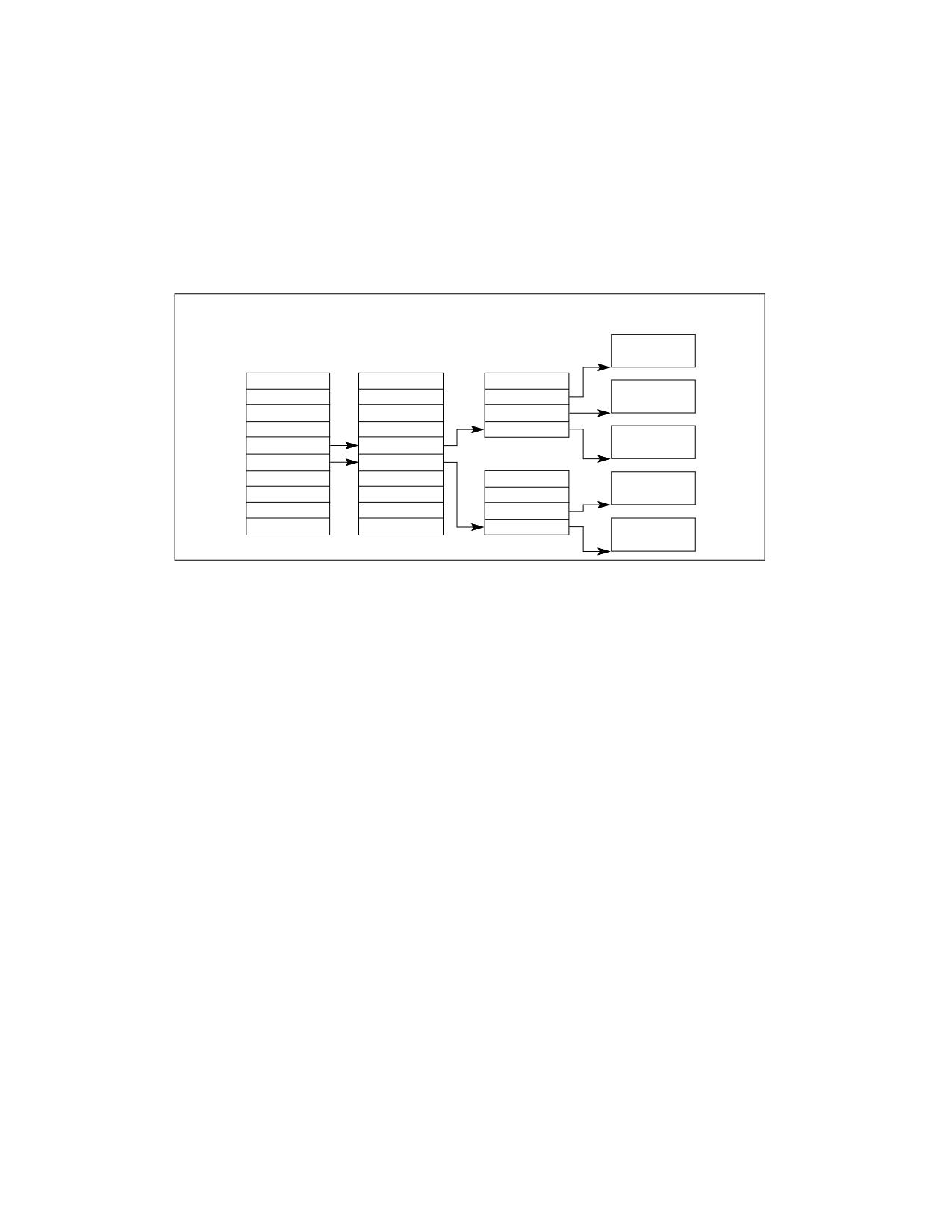
PAGING
The Intel-64 and IA-32 architectures do not enforce correspondence between the boundaries of pages and
segments. A page can contain the end of one segment and the beginning of another. Similarly, a segment can
contain the end of one page and the beginning of another.
Memory-management software may be simpler and more efficient if it enforces some alignment between page and
segment boundaries. For example, if a segment which can fit in one page is placed in two pages, there may be
twice as much paging overhead to support access to that segment.
One approach to combining paging and segmentation that simplifies memory-management software is to give
each segment its own page table, as shown in Figure 5-13. This convention gives the segment a single entry in the
page directory, and this entry provides the access control information for paging the entire segment.
Page Frames
LDT
Page Directory
Page Tables
PTE
PTE
PTE
Seg. Descript.
PDE
Seg. Descript.
PDE
PTE
PTE
Figure 5-13. Memory Management Convention That Assigns a Page Table to Each Segment
Vol. 3A
5-55