HV590L Series Frequency Inverter. User Manual (Version: 3.1.14) - page 5
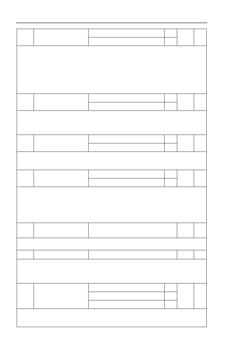
See P5 group for physics DO output
1~40
selection
Short circuit with physics DIx internals
0
A1.13
Virtual VDO3 output function
0
☆
See P5 group for physics DO output
1~40
selection
Short circuit with physics DIx internals
0
A1.14
Virtual VDO4 output function
0
☆
See P5 group for physics DO output
1~40
selection
Short circuit with physics DIx internals
0
A1.15
Virtual VDO5 output function
0
☆
See P5 group for physics DO output
1~40
selection
A1.16
VDO1 output delay time
0.0s~3600.0s
0.0s
☆
A1.17
VDO2 output delay time
0.0s~3600.0s
0.0s
☆
A1.18
VDO3 output delay time
0.0s~3600.0s
0.0s
☆
A1.19
VDO4 output delay time
0.0s~3600.0s
0.0s
☆
A1.20
VDO5 output delay time
0.0s~3600.0s
0.0s
☆
1bit
VDO1
Positive logic
0
Negative logic
1
10bit
VDO2
Positive logic
0
Negative logic
1
100bit
VDO3
Positive logic
0
VDO output terminal
valid
A1.21
00000
☆
state selection
Negative logic
1
1000
VDO4
bit
Positive logic
0
Negative logic
1
10000
VDO5
bit
Positive logic
0
Negative logic
1
Virtual digit output function , which is similar with control board DO output function , can be used to
cooperate with virtual digit input VDIx, to realize some simple logic control.
128
When virtual VDOx output function selecting 0, VDO1~VDO5 output states is determined by input
states of DI1~DI5 on the keyboard.VDOx and DIx one-to-one corresponding.
When virtual VDOx output function selecting non-zero digits, VDOx function setting and use
method are same with P5 group DO output relevant parameters, for details please refer to P5 group.
Similarly, VDOx output valid state can choose positive or negative logic, and set through A1.21.
For VDOx use reference , please refer to applications for VDIx use .
5.20 The second motor control:A2.00-A2.65
HV590L can switch operation between 4 motors. The 4 motors could set motor nameplate
parameters, tune motor parameters, use V/F control or vector control, set encoder relating
parameters and set V/F control or vector control relating parameters respectively.
Groups of A2、A3、A4 are corresponding to motor2、motor3、motor4 respectively. And
the layout of the 3 groups of function codes are completely consistent .
For details please refer to relating parameters of motor1.
Description/
FactoryChange
Code
Setting Range
Keyboard Display
Setting
Limit
General asynchronous motor
0
A2.00
Motor type selection
Variable frequency asynchronous motor
1
0
★
Permanent magnet synchronous motor
2
A2.01
Rated power
0.1kW~1000.0kW
-
★
A2.02
Rated voltage
1V~2000V
-
★
0.01A~655.35A(Inverter power <=55kW)
A2.03
Rated current
-
★
0.1A~6553.5A(Inverter power >55kW)
A2.04
Rated frequency
0.01Hz~maximum frequency
-
★
A2.05
Rated revolving speed
1rpm~65535rpm
-
★
Asynchronous motor stator
0.001Ω~65.535Ω(Inverter power <=55kW)
A2.06
-
★
resistance
0.0001Ω~6.5535Ω(Inverter power >55kW)
Asynchronous motor rotor
0.001Ω~65.535Ω(Inverter power <=55kW)
A2.07
-
★
resistance
0.0001Ω~6.5535Ω(Inverter power >55kW)
Asynchronous motor leakage
0.01mH~655.35mH(Inverter power <=55kW)
A2.08
-
★
inductance
0.001mH~65.535mH(Inverter power >55kW)
Asynchronous motor mutual
0.1mH~6553.5mH(Inverter power <=55kW)
A2.09
-
★
inductance
0.01mH~655.35mH(Inverter power >55kW)
Asynchronous motor no load
0.01A~A2.03(Inverter power <=55kW)
A2.10
-
★
current
0.1A~A2.03(Inverter power >55kW)
A2.27
Encoder pulses number
1~65535
2500
★
ABZ incremental encoder
0
UVW incremental encoder
1
A2.28
Encoder type
0
★
Rotary transformer
2
Sine/cosine encoder
3
129
UVW encoder
4
Local PG
0
A2.29
Speed feedback PG selection
Expansion PG
1
0
★
PULSE pulse input(DI5)
2
ABZ incremental encoder AB
Forward
0
A2.30
0
★
phase
Reserve
1
A2.31
Encoder installation angle
0.0°~359.9°
0
0
★
Forward
0
A2.32
UVW phase sequence
0
★
Reverse
1
A2.33
UVW encoder offset angle
0.0°~359.9°
0.00
★
A2.34
Rotary transformer pole pairs
1~65535
1
★
No action
0.0s
A2.36
PG dropped inspection time
0.0s
★
0.1s~10.0s
0.1s
No operation
0
Asynchronous static tuning
1
A2.37
Tuning selection
Asynchronous complete tuning
2
0
★
Synchronous static tuning
11
Synchronous complete tuning
12
A2.38
Speed loop proportional gain 1
1~100
30
☆
A2.39
Speed loop integration time1
0.01s~10.00s
0.50s
☆
A2.40
Switching frequency1
0.00~A2.43
5.00Hz
☆
A2.41
Speed loop proportional gain 2
0~100
20
☆
A2.42
Speed loop integration time 2
0.01s~10.00s
1.00s
☆
A2.43
Switching frequency 2
A2.40~maximum output frequency
10.00Hz
☆
A2.44
Vector control slip gain
50%~200%
150%
☆
A2.45
Speed-loop filtering time
0.000s~0.100s
0.000s
☆
A2.48 setup
0
AI1
1
AI2
2
Torque upper limit source in
AI3(Potentiometer)
3
A2.47
0
☆
speed control mode
PULSE setup
4
Communication setup
5
MIN(AI1,AI2)
6
MAX(AI1,AI2)
7
130
Torque upper limit digital
A2.48
setup in speed control
0.0%~200.0%
150.0%
☆
mode
Excitation regulation
A2.51
0~60000
2000
☆
proportional gain
Excitation regulation
A2.52
0~60000
1300
☆
integration gain
Torque requlation
A2.53
0~60000
2000
☆
proportional gain
Torque regulation
A2.54
0~60000
1300
☆
integration gain
1bit
Integration separation
Speed loop integration
A2.55
Invalid
0
0
☆
attribute
Valid
1
Speed sensorless vector control(SVC)
0
A2.61
Motor2 control mode
Speed sensor vector control(FVC)
1
0
★
V/F control
2
Same with the first motor
0
Acceleration time1
1
Motor 2 acc./dec. time
A2.62
Acceleration time 2
2
0
☆
selection
Acceleration time 3
3
Acceleration time 4
4
Auto torque hoist
0.0%
A2.63
Motor 2 torque hoist
-
☆
0.1%~30.0%
Motor 2 oscillation
A2.65
0~100
-
☆
suppression gain
5.21 The third motor control: A5.00-A5.09
Description/
FactoryChange
Code
Setting Range
Keyboard Display
Setting
Limit
DPWM switching frequency
A5.00
0.00Hz~15.00Hz
12.00Hz
☆
upper limit
A5.00 is only valid for VF control mode. In asynchronous motor VF running mode, square wave
dertermines the continuous modulation mode. Wave value<A5.00:7-stage continuous modulation
mode. Wave value>A5.00:5-stage continuous modulation mode.
In 7-stage continuous modulation mode, inverter switch loss is relatively big, but current ripple is
small. In 5-stage continuous modulation mode, inverter switch loss is relatively small, but current ripple
is big. High frequency may lead to motor operation instability, generally there is no need of modification.
For VF operation instability please refer to P3.11. For inverter loss and temperature rise please
refer to P0.15.
131
Asynchronous modulation
0
A5.01
PWM modulation mode
0
☆
Synchronous modulation
1
This parameter is only valid for VF control mode. Asynchronous modulation refers to carrier
frequency that linear changes with output frequency, and ensure that the ratio of them (carrier ratio)
remains the same. Generally high output frequency is benefit for output voltage quality.
Generally, synchronous modulation is not needed at low frequencies ( below 100Hz), because the
ratio of carrier frequency and output frequency is relatively high,asynchronous modulation advantage is
more obvious.
When running frequency is greater than 85Hz, synchronous modulation is valid. And fixed as
asynchronous modulation mode when below this frequency.
Dead-zone compensation
No compensation
0
A5.02
1
☆
mode selection
Compensation mode 1
1
Generally speaking , A5.02 needs not to be modified. Only when the output voltage waveform quality
has special requirements or motor appears abnormal phenomenon would users switch the compensation
mode.
Random PWM invalid
0
A5.03
Random PWM depth
0
☆
PWM carrier frequency randomdepth
1~10
Set the random PWM, monotonous and harsh electromagnetic noise can be changed to the
heterogeneous and soft, the external electromagnetic interference can be effectively reduced.
0
indicates that the PWM is invalid. Different random PWM depth represents different regulation effect.
Invalid
0
A5.04
Rapid current-limiting enable
1
☆
Valid
1
Enable the rapid current-limiting function so as to minimize inverter overcurrent protection fault and
make the inverter work normally.
If the inverter long time continuous staying in rapid current-limiting state, it may occur overheating
fault, which is not allowed during operation. Fault alarm of long time rapid current-limiting is 40= Err40 ,
which refers to inverter overload and necessary stop.
Current detection
A5.05
0~100
5
☆
compensation
It is used to set inverter current detection compensation. Excessive setting may lead to decrease of
control performance.Generally do not need to be modified.
A5.06
Under-voltage point setup
60.0%~140.0%
60.0%
☆
A5.06 is used to set value of inverter under-voltage fault 9= E.LU. Different voltage level of 100.0%
corresponds to different voltage point,respectively:
Single phase 220V or three-phase 220V:220V
Three-phase 380V:350V
Three phase 480V:450V
Three-phase 690V:650V
No optimization
0
SVC optimization mode
A5.07
Optimization mode 1
1
1
☆
selection
Optimization mode 2
2
0:No optimization
1: Optimization mode 1
It is used when there is high torque control linearity requirements.
132
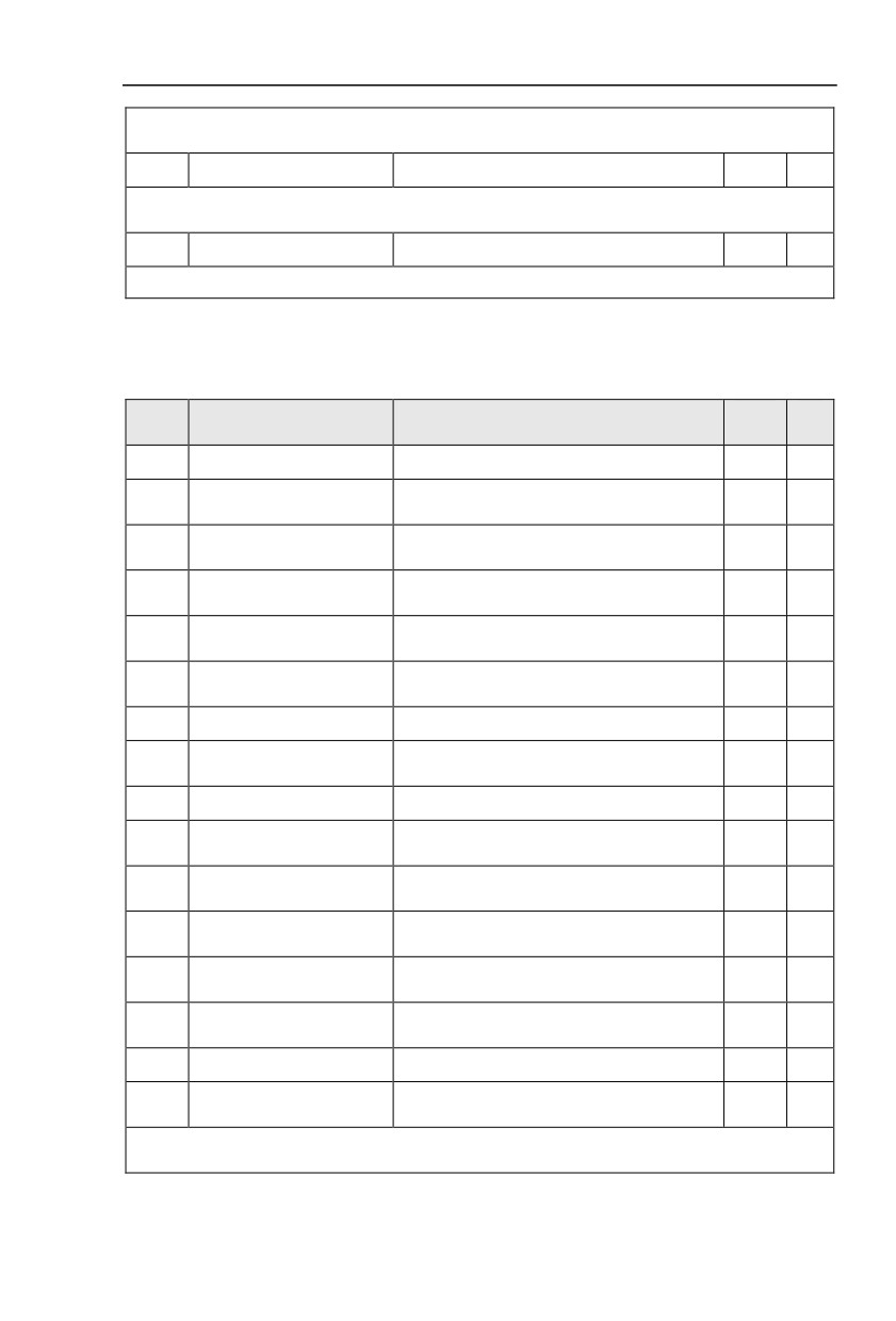
2: Optimization mode 2
It is used when there is high speed stability requirement.
A5.08
Dead zone time adjustment
100%~200%
150%
☆
This parameter is set according to 1140V voltage level. By adjusting the value can improve the
voltage effective use rate. Users are not suggested to modify.
A5.09
Overvoltage point setup
200.0V~2500.0V
810.0V
☆
A5.09 is overvoltage point set through software, which is not related to hardware overvoltage point.
5.22 AI curve setup: A6.00-A6.29
Description/
FactoryChange
Code
Setting Range
Keyboard Display
Setting
Limit
A6.00
AI curve 4 minimum input
-10.00V~A6.02
0.00V
☆
AI curve 4 minimum input
A6.01
-100.0%~100.0%
0.0%
☆
corresponding setup
AI curve
4inflection point
1
A6.02
A6.00~A6.04
3.00V
☆
input
AI curve 4 inflection point 1
A6.03
-100.0%~100.0%
30.0%
☆
input corresponding setup
AI curve 4 inflection point 2
A6.04
A6.02~A6.06
6.00V
☆
input
AI curve 4 inflection point 2
A6.05
-100.0%~100.0%
60.0%
☆
input corresponding setup
A6.06
AI curve 4 maximum input
A6.06~10.00V
10.00V
☆
AI curve 4 maximum input
A6.07
-100.0%~100.0%
100.0%
☆
corresponding setup
A6.08
AI curve 4 minimum input
-10.00V~A6.10
-10.00V
☆
AI curve 5 minimum input
A6.09
-100.0%~100.0%
-100.0%
☆
corresponding setup
AI curve 5 inflection point 1
A6.10
A6.08~A6.12
-3.00V
☆
input
AI curve 5 inflection point 1
A6.11
-100.0%~100.0%
-30.0%
☆
input corresponding setup
AI curve 5 inflection point 2
A6.12
A6.10~A6.14
3.00V
☆
input
AI curve 5 inflection point 2
A6.13
-100.0%~100.0%
30.0%
☆
input corresponding setup
A6.14
AI curve 5 maximum input
A6.12~10.00V
10.00V
☆
AI curve 5 maximum input
A6.15
-100.0%~100.0%
100.0%
☆
corresponding setup
Function of curve 4 and curve 5 are similar with curve 1~curve 3’s. Curve 1~curve 3 are straight
lines, while curve 4 and curve 5 are 4-point curves which could realize more flexible correspondence.
133
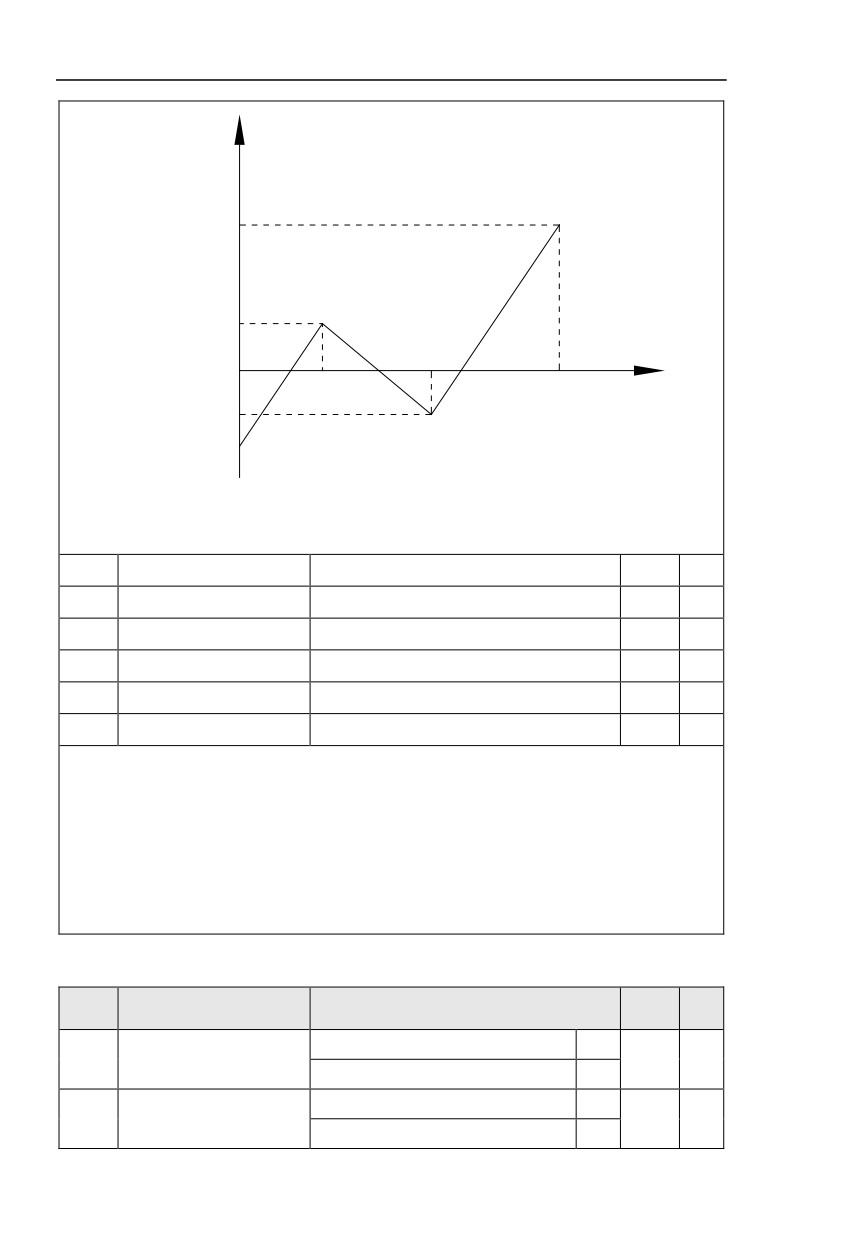
Analog input
100%
corresponding setting
AI maximum input
corresponding setting
AI inflection point 1
corresponding setting
AI input voltage
AI inflection point 2
0V(0mA)
AI inflection point 1
10V(20mA)
AI inflection point 2
corresponding setting
AI minimum input
corresponding setting
-100%
Fig.5-32Curve4 and curve 5 schematic diagram
Notice:When setting curve 4 and curve 5, minimum input voltage, inflection point 1 voltage,
inflection point 2 voltage and maximum voltage must be increased in turn.
A6.24
AI1 set hopping point
-100.0%~100.0%
0.0%
☆
A6.25
AI1 set hopping amplitude
0.0%~100.0%
0.5%
☆
A6.26
AI2 set hopping point
-100.0%~100.0%
0.0%
☆
A6.27
AI2 set hopping amplitude
0.0%~100.0%
0.5%
☆
A6.28
AI3 set hopping point
-100.0%~100.0%
0.0%
☆
A6.29
AI3 set hopping amplitude
0.0%~100.0%
0.5%
☆
Analog input AI1~AI3 of HV590L are all provided with hopping function for set value.
Hopping frequency refers to fixing of analog corresponding setup to the value of hopping point
when analog correspondending setting varies within jump point upper/lower limit.
E.g:
Voltage of analog input AI1 is in 5.00V fluctuation, which range is 4.90V~5.10V. Minimum input
0.00V corresponding to 0.0%, while maximum input 10.00V corresponding to 100.%.The corresponding
setting of AI1 fluctuates between 49.0%~51.0%.
Set A5.16 to 50.0% and A5.17 to 1.0%, after hopping function processing, AI1 is fixed as 50.0%. In
this way, AI1 is converted into a stable input, and fluctuation is eliminated.
5.23 User programmable card parameters: A7.00-A7.09
Description/
FactoryChange
Code
Setting Range
Keyboard Display
Setting
Limit
Invalid
0
User programmable function
A7.00
0
★
selection
Valid
1
Inverter control
0
Control board output terminal
A7.01
-
★
control mode selection
User programmable card control
1
134
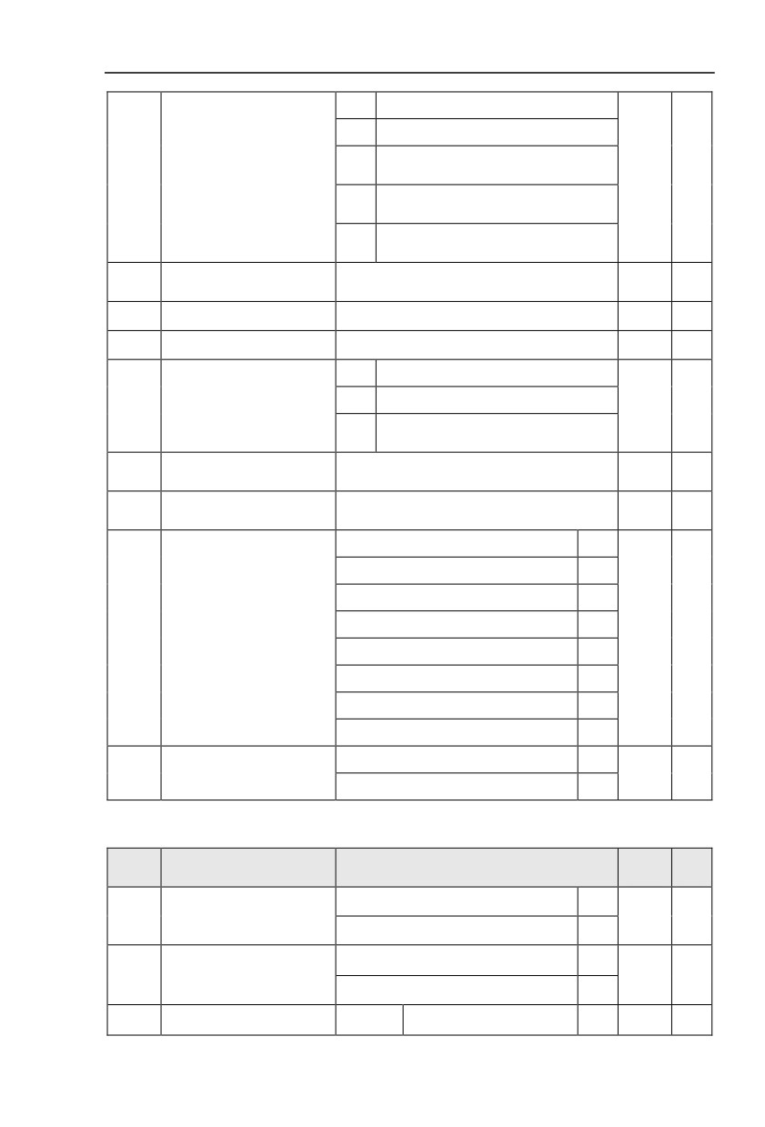
1bit
Y1P(Y1 as pulse output)
10bit
Relay(T/A1-T/B1-T/C1)
100
DO1
bit
1000
Y1R(Y1 as switch output)
bit
10000
AO1
bit
Programmable card expansion
See 《 User programmable control card 》 for
A7.02
-
★
AI3x function configuration
supplementary description
A7.03
Y1P output
0.0%-100.0%
0.0%
☆
A7.04
AO1 output
0.0%-100.0%
0.0%
☆
1bit
Y1R
10bit
Relay 1
A7.05
Switch output
000
☆
100
DO
bit
Programmable card
A7.06
0.0%-100.0%
0.0%
☆
frequency setup
Programmable card torque
A7.07
-200.0%-200.0%
0.0%
☆
setup
No command
0
Forward command
1
Reverse command
2
Forward jog
3
Programmable card
A7.08
0
☆
command setup
Reverse jog
4
Free stop
5
Decelerate to stop
6
Fault reset
7
No fault
0
Programmable card fault
A7.09
0
☆
setup
Fault code
80-89
5.24 Point to point communication:A8.00-8.11
Description/
FactoryChange
Code
Setting Range
Keyboard Display
Setting
Limit
Invalid
0
Master slave control
A8.00
0
☆
function selection
Valid
1
Master
0
A8.01
Master slave selection
0
☆
slave
1
A8.02
0 bit
Do not follow
the
0
011
☆
Master slave information
135
exchange
Mastercommand
follow the Master command
1
10 bit
Do notsend fault information
0
send fault information
1
100 bit
Do notwarning when slave
0
off line
warning when slave off line
1
Master slave control frame
0
A8.03
Message frame selection
0
☆
Droop control frame
1
Receive data zero
-100.00%~100.00%
A8.04
0.00
★
offsettorque
A8.05
Receive data gaintorque
-10.00~100.0
1.00
★
Communication interrupt
0.0s~10.0s
A8.06
1.0s
☆
detection time
Communication Master
0.001s~10.000s
A8.07
0.001
☆
data transmission cycle
Receive data zero
-100.00%~100.00%
A8.08
0.00
★
offsetfrequency
Receive data
-10.00~100.00
A8.09
1.00
★
gainfrequency
A8.10
Reverse
-
A8.11
view
0.20Hz~10.00Hz
0.5
★
5.25 Extended function group:A9.00-A9.09
Description/
FactoryChange
Code
Setting Range
Keyboard Display
Setting
Limit
A9.00
Reverse
0
●
A9.01
Reverse
0~65535
0
☆
A9.02
Reverse
0~65535
0
☆
A9.03
Reverse
0~65535
0
☆
A9.04
Reverse
0~65535
0
☆
A9.05
Reverse
0~65535
0
☆
A9.06
Reverse
0~65535
0
☆
136
A9.07
Reverse
0~65535
0
☆
A9.08
Reverse
0~65535
0
☆
A9.09
Reverse
0~65535
0
☆
5.26 AI/AO correction: AC.00-AC.19
Description/
FactoryChange
Code
Setting Range
Keyboard Display
Setting
Limit
Factory
AC.00
AI1measured voltage 1
0.500V~4.000V
☆
calibration
Factory
AC.01
AI1 display voltage 1
0.500V~4.000V
☆
calibration
Factory
AC.02
AI1 measured voltage 2
6.000V~9.999V
☆
calibration
Factory
AC.03
AI1 display voltage 2
6.000V~9.999V
☆
calibration
Factory
AC.04
AI2 measured voltage 1
0.500V~4.000V
☆
calibration
Factory
AC.05
AI2 display voltage 1
0.500V~4.000V
☆
calibration
Factory
AC.06
AI2 measured voltage 2
6.000V~9.999V
☆
calibration
Factory
AC.07
AI2 display voltage 2
6.000V~9.999V
☆
calibration
Factory
AC.08
AI3 measured voltage 1
-9.999V~10.000V
☆
calibration
Factory
AC.09
AI3 display voltage 1
-9.999V~10.000V
☆
calibration
Factory
AC.10
AI3 measured voltage 2
-9.999V~10.000V
☆
calibration
Factory
AC.11
AI3 display voltage 2
-9.999V~10.000V
☆
calibration
This group of function codes are used for calibration of analog input AI , which could eliminate AI
input bias and gain influence. Generally , there is no need of calibration in application, for it has been
calibrated in factory. When restoring the factory value, the parameter would be restored to the default
value of factory calibration.
Measured voltage refers to the actual voltage that has been measured through measuring
instrument such as multimeter. Display voltage refers to the display value that has been sampled by the
inverter. See U0 group (U0.21、U0.22、U0.23) display.
During calibration, put the multimeter measurement value and the U0 value respectively into the
function codes above, inverter would automatically calibrate the AI zero off and gain.
Factory
AC.12
A01 target voltage 1
0.500V~4.000V
☆
calibration
Factory
AC.13
A01 measured voltage 1
0.500V~4.000V
☆
calibration
Factory
AC.14
A01 target voltage 2
6.000V~9.999V
☆
calibration
AC.15
A01 measured voltage 2
6.000V~9.999V
Factory
☆
137
calibration
Factory
AC.16
A02 target voltage 1
0.500V~4.000V
☆
calibration
Factory
AC.17
A02 measured voltage 1
0.500V~4.000V
☆
calibration
Factory
AC.18
A02 target voltage 2
6.000V~9.999V
☆
calibration
Factory
AC.19
A02 measured voltage 2
6.000V~9.999V
☆
calibration
This group of function codes are used for calibration of analog output AO. Generally , there is no
need of calibration in application, for it has been calibrated in factory. When restoring the factory value,
the parameter would be auto restored to the default value of factory calibration.
Target voltage refers to inverter theoretical output voltage, while measured voltage refers to the
actual voltage that has been measured through measuring instrument such as multimeter.
138
Section VI. Fault Diagnosis & Solutions
HV590L is able to make full use of the device performance, while implementing effective
protection. You may encounter following fault tips during operation, please control the following
table analysis the possible causes, and rule out the fault.
6.1 Fault alarm and solutions
HV590L series can not only make full use of equipment performance but also implement
effective protection. HV590L series has 51 alarming information and protection function.Once
fault occurs, protection function acts,output stops, inverter fault relay contact starts,and fault
code is been displayed on the display panel. Before consulting the service department, the user
can perform self-check according to the prompts of this chapter, analyze the fault cause and find
out t solution. If the fault is caused by the reasons as described in the dotted frame, please
consult the agents or our company directly.
Among the 51 items of warning information:
Fault no.22= Err22refers to hardware over-current or over-voltage signal.In most cases
hardware over-voltage fault led to fault no.22= Err22 alarming.
Fault name
Inverter unit protection
Panel display
Fault No.1= Err01
1、Inverter output loop short circuit
2、Two long wiring between motor and inverter.
3、Module overheating
Fault investigation
4、Inverter internal wiring loose
5、Main control board anomalies
6、Drive board anomalies
7、Inverter module anomalies
1、Eliminate external faults
2、Add reactor or output filter
Fault
3、Check air duct, fan and eliminate existing problems.
countermeasures
4、Insert all connecting wires
5、For technical support
Fault name
Acceleration over current
Panel display
Fault No.2= Err02
1、Acceleration time too short
2、Improper manual torque boost or V/F curve
3、Low voltage
4、Inverter output loop grouded or short circuit
Fault investigation
5、Vector control mode without parameter identification
6、Start the rotating motor
7、Sudden load add in acceleration process
8、Small type selection of inverter.
Fault
1、Increase acceleration time
139
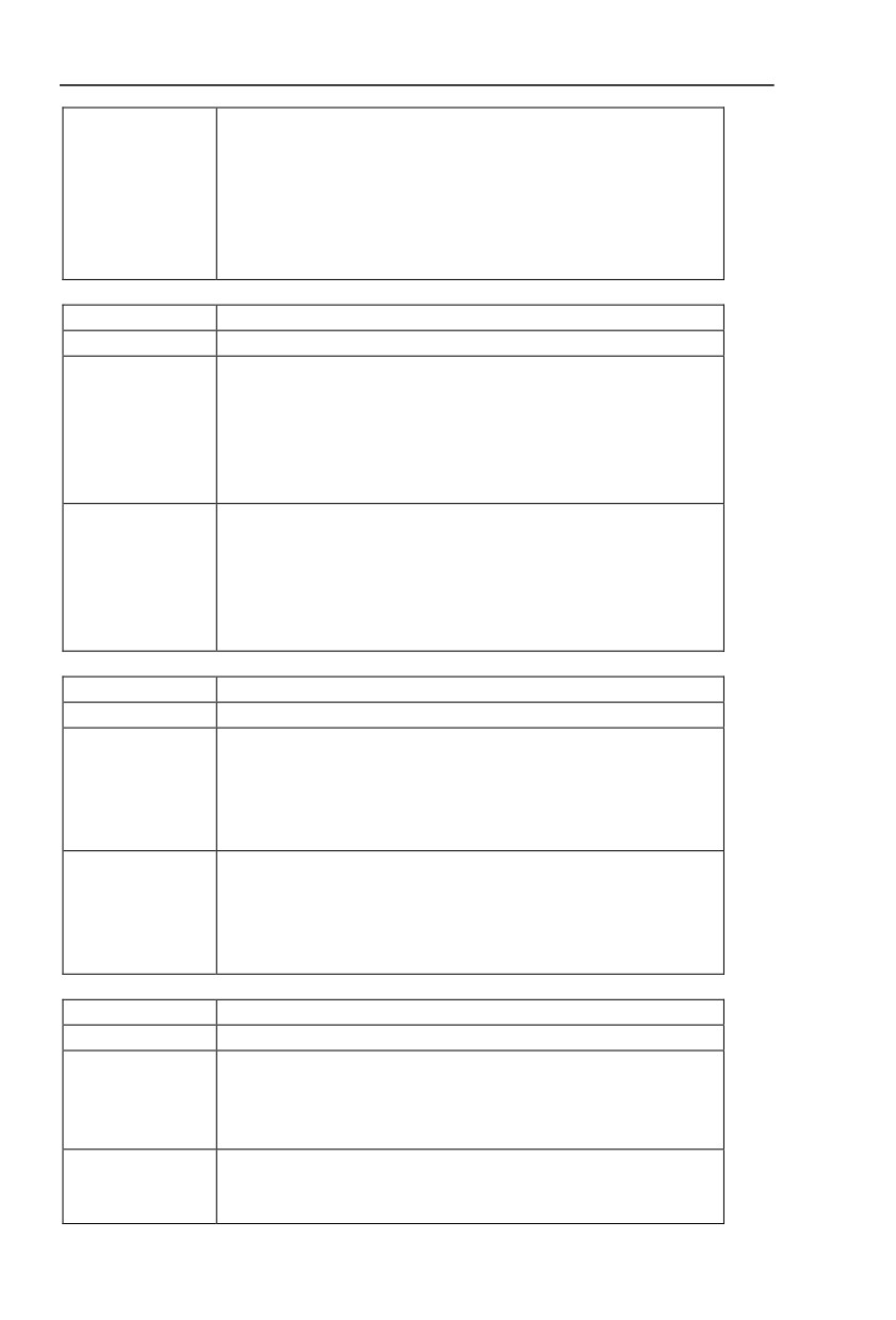
countermeasures
2、Adjust manual torque boost or V/F curve
3、Adjust voltage to normal range
4、Eliminate external faults
5、Parameter identification
6、Select speed tracking start or restart after motor stop
7、Cancel sudden added load
8、Choose inverter of greater power level
Fault name
Deceleration over current
Panel display
Fault No.3= Err03
1、Inverter output loop grouded or short circuit
2、Vector control mode without parameter identification
3、Deceleration time too short
Fault investigation
4、Low voltage
5、Sudden load add in deceleration process
6、No braking unit and brake resistence installed
1、Eliminate external faults
2、Parameter identification
Fault
3、Increase deceleration time
countermeasures
4、Adjust voltage to normal range
5、Cancel sudden added load
6、Install braking unit and brake resistence
Fault name
Constant speed over current
Panel display
Fault No.4= Err04
1、Inverter output loop grouded or short circuit
2、Vector control mode without parameter identification
Fault investigation
3、Low voltage
4、Sudden load add in deceleration process
5、Small type selection of inverter
1、Eliminate external faults
2、Parameter identification
Fault
3、Adjust voltage to normal range
countermeasures
4、Cancel sudden added load
5、Choose inverter of greater power level
Fault name
Acceleration over voltage
Panel display
Fault No.5= Err05
1、No braking unit and brake resistence installed
2、High input voltage
Fault investigation
3、External force drive motor operation during acceleration process
4、Acceleration time too short
1、Install braking unit and brake resistence
Fault
2、Adjust voltage to normal range
countermeasures
3、Cancel external force or install brake resistence
140
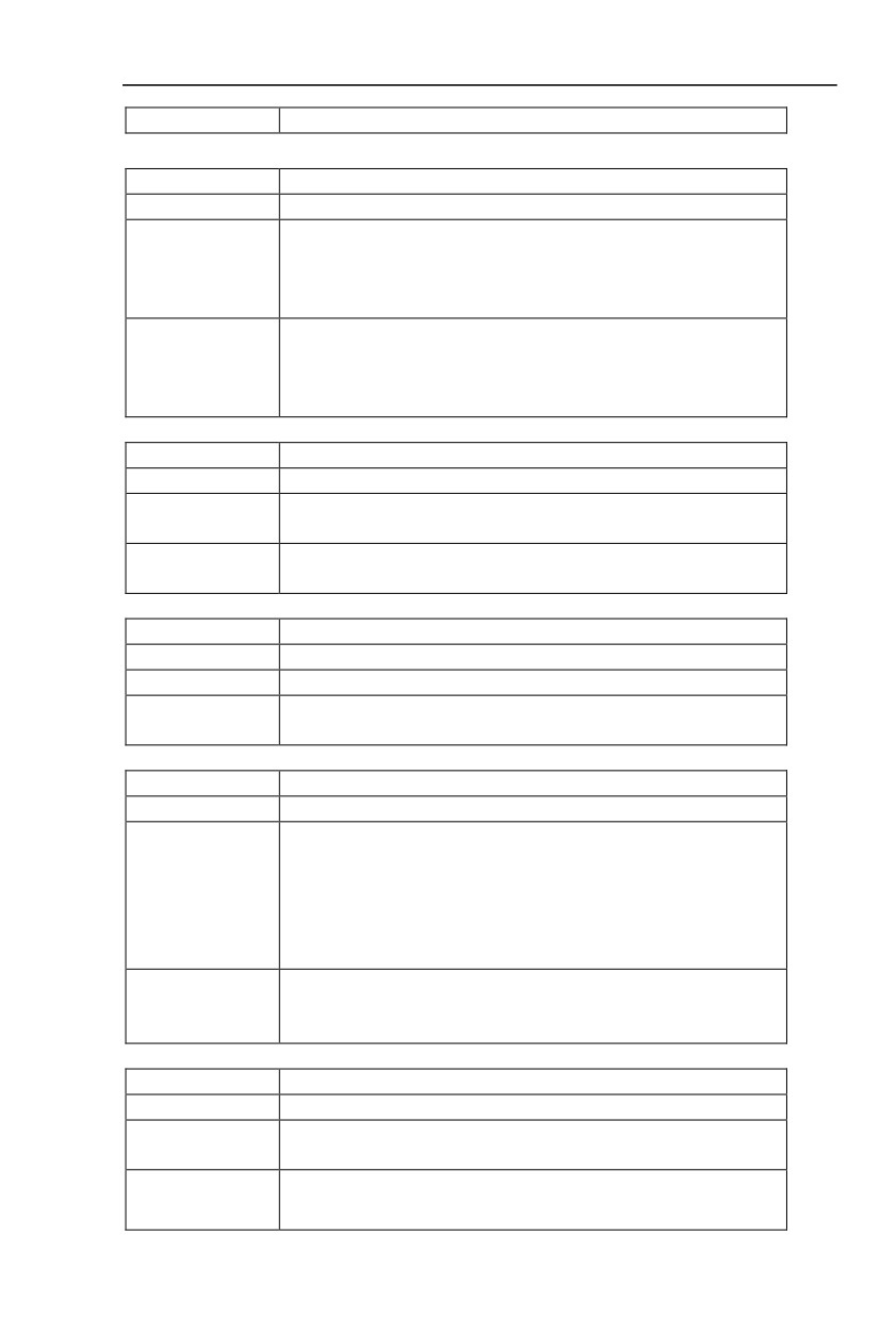
4、Increase acceleration time
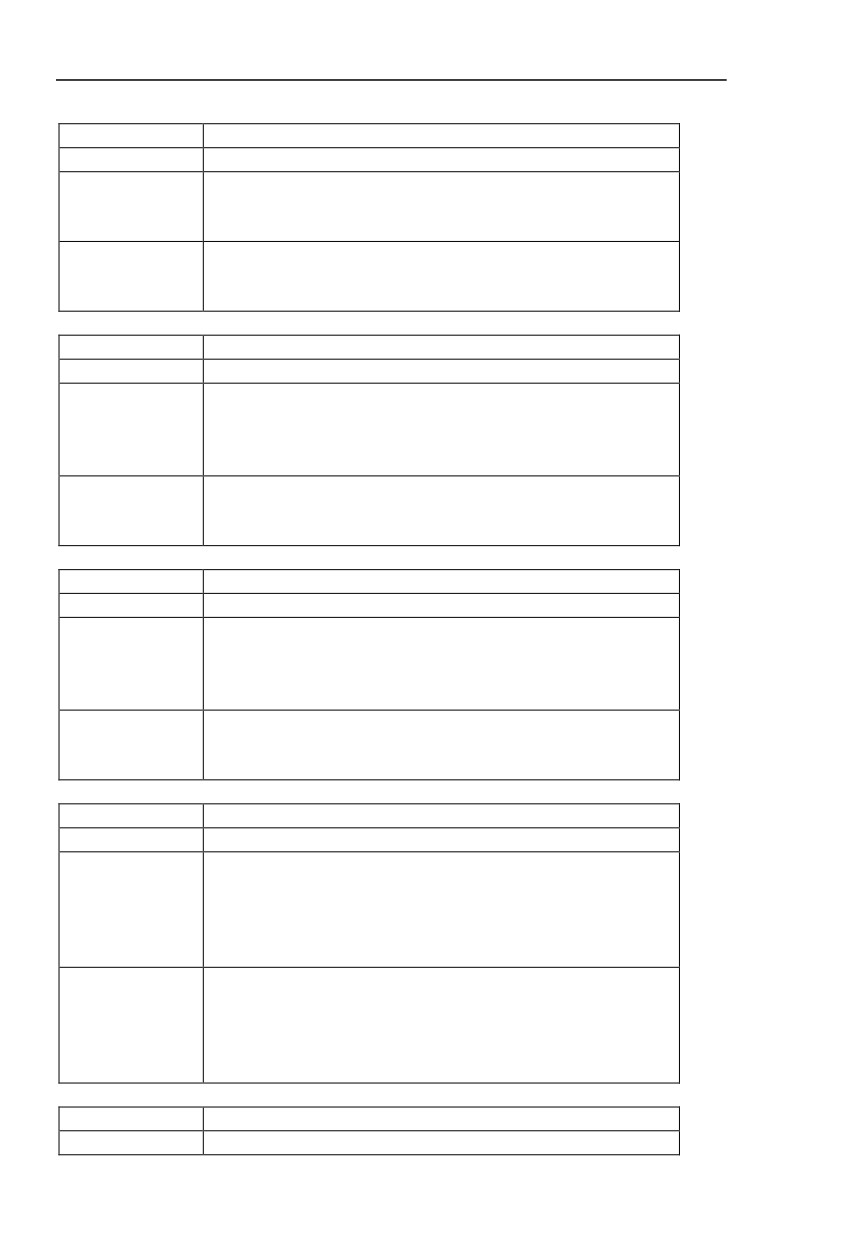
Fault name
Deceleration over voltage
Panel display
Fault No.6= Err06
1、High input voltage
2、External force drive motor operation during deceleration process
Fault investigation
3、Deceleration time too short
4、No braking unit and brake resistence installed
1、Adjust voltage to normal range
Fault
2、Cancel external force or install brake resistence
countermeasures
3、Increase deceleration time
4、Install braking unit and brake resistence
Fault name
Constant speed over voltage
Panel display
Fault No.7= Err07
1、External force drive motor operation
Fault investigation
2、High input voltage
Fault
1、Cancel external force or install brake resistence
countermeasures
2、Adjust voltage to normal range
Fault name
Control power supply fault
Panel display
Fault No.8= Err08
Fault investigation
1、Input voltage is not within the specified range
Fault
1、Adjust voltage to normal range
countermeasures
Fault name
Undervoltage fault
Panel display
Fault No.9= Err09
1、Instantaneous power-off
2、Input voltage is not within the specified range
3、Bus voltage anomalies
Fault investigation
4、Rectifier and buffer resistance anomalies
5、Drive board anomalies
6、Control board anomalies
1、Reset fault
Fault
2、Adjust voltage to normal range
countermeasures
3、For technical support
Fault name
Inverter overload
Panel display
Fault No.10= Err10
1、Small type selection of inverter.
Fault investigation
2、Overload or motor stall
Fault
1、Choose inverter of greater power level
countermeasures
2、Reduce the load and check the motor and mechanical condition
141
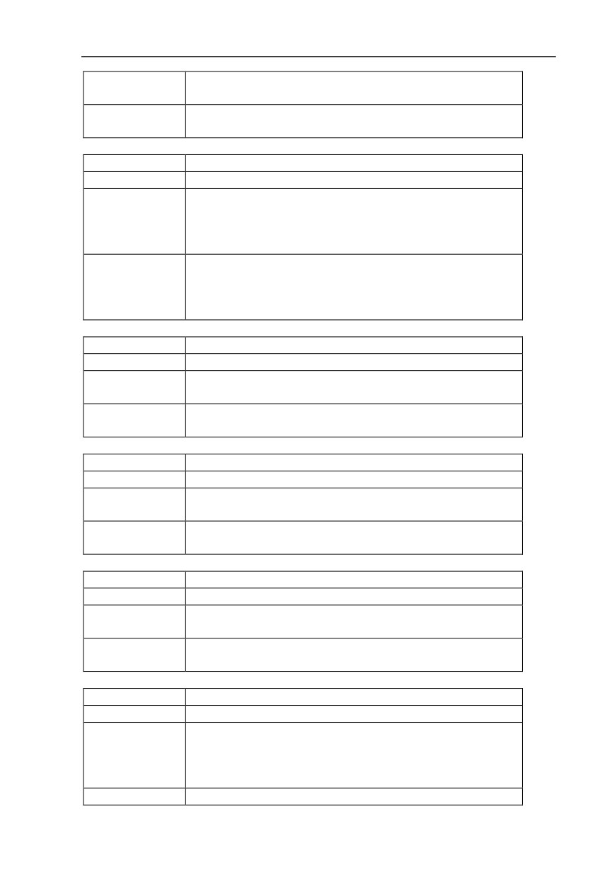
Fault name
Motor overload
Panel display
Fault No.11= Err11
1、Small type selection of inverter
Fault investigation
2、Improper setup of P9.01
3、Overload or motor stall
1、Choose inverter of greater power level
Fault
2、Set P9.01 correctly
countermeasures
3、Reduce the load and check the motor and mechanical condition
Fault name
Input phase lack
Panel display
Fault No.12= Err12
1、Drive board anomalies
2、Lightning protection board (BESP ) anomalies
Fault investigation
3、Control board anomalies
4、3-phase input power-supply anomalies
1、Replace driver, power- supply board or contactor
Fault
2、For technical support
countermeasures
3、Eliminate external loop faults
Fault name
Output phase lack
Panel display
Fault No.13= Err13
1、Wiring between motor and inverter anomalies
2、Inverter unbalanced 3-phase output
Fault investigation
3、Drive board anomalies
4、Module anomalies
1、Eliminate external loop faults
Fault
2、Check 3-phase winding and eliminate faults
countermeasures
3、For technical support
Fault name
Module overheating
Panel display
Fault No.14= Err14
1、Air duct block
2、Fan damage
Fault investigation
3、High ambient temperature
4、Module thermistor damage
5、Inverter module damage
1、Clean air dust
2、Replace the fan
Fault
3、Reduce ambient temperature
countermeasures
4、Replace thermistor
5、Replace inverter module
Fault name
External equipment fault
Panel display
Fault No.15= Err15
142
1、Input external fault signal through DI
Fault investigation
2、Input external fault signal through IO
Fault
1、Reset operation
countermeasures
Fault name
Communication fault
Panel display
Fault No.16= Err16
1、Abnornal communication cable
2、Wrongly set communication expansion card P0.28
Fault investigation
3、Wrongly set communication parameter PD group
4、Position machine operation anomalies
1、Check the communication cable
Fault
2、Set communication expansion card type correctly
countermeasures
3、Set communication parameter correctly
4、Check position machine cable
Fault name
Contactor fault
Panel display
Fault No.17= Err17
1、Input phase lack
Fault investigation
2、Drive board , contactor anomalies
Fault
1、Eliminate external loop faults
countermeasures
2、Replace driver, power- supply board or contactor
Fault name
Current inspection fault
Panel display
Fault No.18= Err18
1、Drive board anomalies
Fault investigation
2、Hall devices anomalies
Fault
1、Replace drive board
countermeasures
2、Replace hall devices
Fault name
Motor tuning fault
Panel display
Fault No.19= Err19
1、Parameter identification process overtime
Fault investigation
2、Wrongly set motor parameters
Fault
1、Check wire between inverter and motor
countermeasures
2、Set motor parameters correctly according to the nameplate
Fault name
Encoder /PG card fault
Panel display
Fault No.20= Err20
1、Encoder anomalies
2、PG card anomalies
Fault investigation
3、Encoder type mismatch
4、Encoder connections fault
Fault
1、Replace encoder
143
countermeasures
2、Replace PG card
3、Set motor encoder type correctly
4、Eliminate circuit faults
Fault name
EEPROM read & write fault
Panel display
Fault No.21= Err21
Fault investigation
1、EEPROM chip damage
Fault
1、Replace main control board
countermeasures
Fault name
Inverter hardware fault
Panel display
Fault No.22= Err22
1、Presence of overvoltage
Fault investigation
2、Presence of overcurrent
Fault
1、Treat according to overvoltage fault
countermeasures
2、Treat according to overcurrent fault
Fault name
Short circuit to ground fault
Panel display
Fault No.23= Err23
Fault investigation
1、Motor short circuit to ground
Fault
1、Replace cable or motor
countermeasures
Fault name
Total running time arrival fault
Panel display
Fault No.26= Err26
Fault investigation
1、Total running time arrive the set value
Fault
1、Clear record information using parameter initialization function
countermeasures
Fault name
User-defined fault 1
Panel display
Fault No.27= Err27
1、Input user-defined fault 1 signal through multi-function terminal DI
Fault investigation
2、Input user-defined fault 1 signal through virtual IO function
Fault
1、Reset operation
countermeasures
Fault name
User-defined fault 2
Panel display
Fault No.28= Err28
1、Input user-defined fault 2 signal through multi-function terminal DI
Fault investigation
2、Input user-defined fault 2 signal through virtual IO function
Fault
1、Reset operation
countermeasures
Fault name
Total power-on time arrival fault
144
Panel display
Fault No.29= Err29
Fault investigation
1、Total power-on time arrive the set value
Fault
1、Clear record information using parameter initialization function
countermeasures
Fault name
Load off fault
Panel display
Fault No.30= Err30
Fault investigation
1、Inverter running current less than P9.64
Fault
1、Confirm whether load off or P9.64, P9.65parameter settings is
countermeasures
inaccordance with the actual operating condition
Fault name
PID feedback loss during operation fault
Panel display
Fault No.31= Err31
Fault investigation
1、PID feedback less than PA.26 set value
Fault
1、Check PID feedback signal or set PA.26 to a proper value
countermeasures
Fault name
Each wave current limiting fault
Panel display
Fault No.40= Err40
1、Excessive load or motor stall
Fault investigation
2、Small type selection of inverter.
Fault
1、Reduce the load and check the motor and mechanical condition
countermeasures
2、Choose inverter of greater power level
Fault name
Motor switching fault
Panel display
Fault No.41= Err41
Fault investigation
1、Change current motor selection during inverter operation
Fault
1、Switch the motor after inverter stopped.
countermeasures
Fault name
Excessive speed deviation fautl
Panel display
Fault No.42= Err42
1、Improper set inspection parameters P9.69、P9.60
Fault investigation
2、Wrongly set encoder parameters
3、No parameter identification
1、Set inspection parameters properly according to actual situation
Fault
2、Set motor encoder parameters correctly
countermeasures
3、Motor parameter identification
Fault name
Motor overspeed fault
Panel display
Fault No.43= Err43
1、No parameter identification
Fault investigation
2、Wrongly set encoder parameters
3、Improper set inspection parameters P9.69、P9.60
145
1、Motor parameter identification
Fault
2、Set motor encoder parameters correctly
countermeasures
3、Set inspection parameters properly according to actual situation
Fault name
Motor overtemperature fault
Panel display
Fault No.45= Err45
1、Temperature sensor wiring loose
Fault investigation
2、Motor overtemperature
Fault
1、Check sensor wiring and eliminate fault
countermeasures
2、Reduced carrier frequency or take other cooling measures for the motor
Fault name
Initial position fault
Panel display
Fault No.51= Err51
Fault investigation
1、Excessive deviation between motor parameters and the paractical value
Fault
1、Reconfirm motor parameter settings, pay attention to the rated current
countermeasures
value
6.2 Common fault and solutions
During the inverter using process, the following faults may occur. Please conduct simple
fault analysis by referring to the methods below:
Fault
No.
Possible Cause
Solution
Phenomenon
Abnormal
input
power
supply,switch power supply
fault of driven board, rectifier
bridge damage, inverter
Check inputpower supply, bus voltage,
No display or error codes
1
buffer resistance damage,
re-plug
26
core
cable,
occur upon power-on
control board/keyboard fault,
consultthemanufacturer
control
board/driven
board/keyboard
disconnection
Poor contact between driven
board and control board,
device damage on control
Re-plug 26 core cable,
2
Display“510” upon power-on
board, motor or motor cable
consult the manufacturer
short circuited, hall fault, grid
undervoltage
The motor or the output line
Measure the insulationof the motor and
“Error 23=Err23” alarming
is short circuited to the
3
output line with magneto-ohmmeter,
upon power on
earth
、 the inverter is
consult themanufacturer.
damaged.
The inverter displays
normally upon power-on,
The fan is either damaged or
Replace the fan,exclude external short-
4
but “510” is displayed upon
blocked,
peripheral
circuit fault
running and stops
controlterminalshortcircuited
immediately
The carrier frequency is set too
Frequent fault
Replace the fan,clean air duct, reduce
high, the fan is damaged or the
5
reportERR14=Err14(module
carrier
air duct is blocked, inverter
overheating)
frequency(P0.15) ,consultmanufacturer.
internal components damaged
Motor no rotating after
Motor or motor cable,
Replace the motor orremove the
6
inverter power-on
wrongly set inverter
mechanical fault, check and reset the
146

parameters(motor
parameters, confirm connection between
parameter), poor contact
inverter and motor
between driven board and
control board, driven board
fault
Wrongly set inverter
Check and reset the P4relevant
parameters, wrong external
parameters,reconnect cables, reconfirm
7
DI terminal invalid
signal, SP and +24V jumper
PLC and +24V jumper, consultthe
loosening, control board fault
manufacturer.
Encoder fault; PG card fault;
Closed loop vector control,
drive board fault; encoder
Replace encoder&reconfirm connections;
8
motor speed cannot
wrong connection or poor
replace PG card; consultmanufacturer.
ascend
contact
The inverter frequently
Motor wrongly set
Reset motor parameters or motor tuning,
9
reports over current fault &
parameters,improper
set proper
over voltage fault
acc./dec. time, load fluctuation
acc./dec.time,consultmanufacturer.
Caution:
※ After power off and within 5 minutes of charging indicator light(!CHARGE)out , please do
not touch any spare parts inside the machine. The operator must use instrument to confirm
capacitor discharge is comleted, then could implement machine operation, or there may be
electric shock risk!
※ Please do not touch the printed circuit board and IGBT etc internal device without
electrostatic prevention measures. Or it could lead to the damage of components.
147
Section VII. Inspection & Maintenance
7.1 Inspection and Maintenance
Under normal working conditions, in addition to daily inspection, the frequency converter
should be subject to regular inspection (for example inspection for overhaul or as specified but
at an interval of at most six months). Please refer to the following table in order to prevent faults.
Daily
Regular
Check item
Check details
Method
Criterion
LED display
If any abnormal display
Visual check
As per use state
√
If any abnormal noise or
√
√
Fan
Visual and audible check
No anomalies
vibration
Surrounding
Temperature, humidity, dust
Visual\audible\sensory
√
As per 2-1 item
conditions
content, harmful gas, etc.
check
Input output
If any abnormal input, output
Measure R, S, T and
As per standard
√
voltage
voltage
U, V, W terminals
specifications
Fasteners whether loose, if
any signs showing overheat,
Check visually, tighten
Main circuit
discharging, or too high dust
the fastenings, and clean
No anomalies
√
content, or the air piping is
the related parts
blocked
Electrolytic
If any abnormal appearance
Check visually
No anomalies
√
capacitor
Current-conducting
√
Loose or not
Check visually
No anomalies
leads or blocks
Tighten the loose
Terminals
If the screws or bolts loose
No anomalies
√
screws or bolts
“√” means need daily check or regularly check.
For inspection,do not disassemble or shake the parts without reason, or pull off the plug-in-
parts at random. Otherwise, the unit will not operate normally, or can not enter the mode of fault
display, or causes faults of components or even parts of the main switch components IGBT
module is damaged.
When needing measurement, the user should note that much different results will be gained
possibly if the measuring is performed with different instruments. It is recommended that the
input voltage be measured with pointer-type voltmeter, output voltage with rectification voltmeter,
input and output current with tong-test ammeter, and power with electrically-driven wattmeter.
148
7.2 Regular replacement of the device
In order to ensure the operation reliability of the frequency converter, in addition to regular
maintenance and inspection, all the parts suffering long-term mechanical wear should be
replaced at a regular interval, which includes all cooling fans and the filtering capacitors of main
circuits for energy buffer and interchange and PCBs. For continuous use under normal
conditions, these parts can be replaced according to the following table and the operating
environment, loads and the current state of frequency converter.
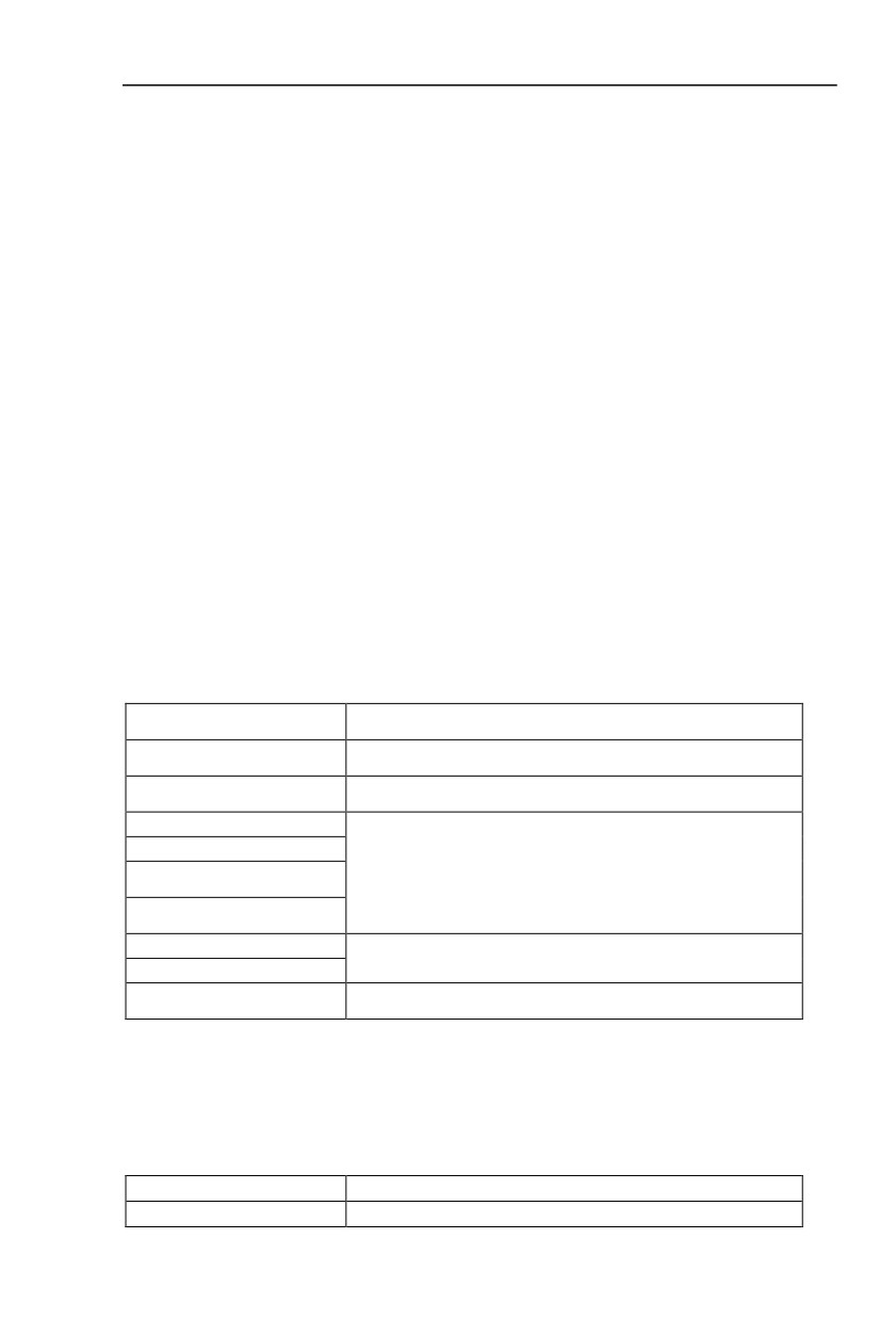
Part name
Standard replacement years
Cooling fan
1~3 years
Filtering capacitor
4~5 years
PCB
5~8 years
(printed circuit board)
7.3 Storage
The following actions must be taken if the frequency converter is not put into use
immediately after delivery to the user and need to keep well for the time being or stored for a
long time:
※ Stored in a dry and adequately-ventilated place without dust and metal powder at the
temperature specified in the specifications.
※ If the frequency converter is not put into use after one year, a charge test should be made,
so as to resume the performance of the filtering capacitor of main circuit in it. For charging,
a voltage regulator should be used to slowly increase the input voltage of the frequency
converter until it reaches the rating, and the charge should last more than 1~2 hours. This
test should be made at least once a year.
※ Don’t perform breakdown test at random, for this test will cause shorter life of the frequency
converter. The insulation test must be performed after the insulation resistance is measured
with a 500-volt mega ohm and this value must not be less than 4MΩ.
7.4 Measuring and Judgment
※ If the current is measured with the general instrument, imbalance will exists for the current
at the input terminal. Generally, differing by not more than 10% is normal. If it differs by 30%,
inform the factory to replace the rectification bridge, or check if the error of three-phase
input voltage is above 5V.
※ If the three-phase output voltage is measured with a general multi-meter, the read data is
not accurate due to the interference of carrier frequency and only for reference.
7.5 Safety Precaution
※ Only specially trained persons are allowed to disassembly,replace the drive components.
※ Before the inspection and maintenance,inverter must be confirmed at least 5 minutes after
149
power off or charged(CHARGE) light is off,otherwise there is risk of electric shock.
※ Avoid metal parts leaving in the drive, or it may result in equipment damage.
150

Appendix I H5RS485 Card & RS485Communication Protocol
I.1 H5RS485 card
H5RS485 card produced by HNC is used with HV590L series inverter as RS485
communication card. It contains the following resources:
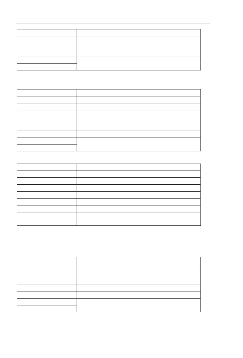
Table 2Jumper description
Jumper number
Description
J1
SP1 connection mode selection
J2
RS485 Termination resistor selection
I.2 Communication protocol
I.2.1 Protocol content
The serial communication protocol defines the information content and format of the
use of the transmission in serial communication. Including: the host polling (or broadcast)
format、host encoding methods.Concent including: require action of the function code,
data transmission and error checking and so on. Slave machine's response is the same
structure, including: action confirmation, return data and error checking. Slave error
occurred when receiving information, or can not do what the host request action, it will
organize a fault messageas the response back to the host computer.
Application mode:
The inverter accessing with “ single main multi-slave” PC/PLC control network which
equipped with RS232/RS485 bus.
Bus structure:
(1) Interface mode
RS232/RS485 hardware interface
(2) Transmission mode
Asynchronous serial, half-duplex transmission. At the same time host and slave
computer can only permit one to send data while the other can only receive data. Data in
the process of serial asynchronous communication is in the message format and sent one
frame by one frame.
(3) Topological mode
In single-master system, the setup range of slave address is 1 to 247. Zero refers to
broadcast communication address. The address of slave must is exclusive in the network.
That is one condition of one slave machine.
I.3 Protocol Description
HV590L series inverter communication protocol is an asynchronous serial master-slave
Modbus communication protocol, only one device in the network
(master) to establish
protocol (known as the "query / command"). Other device (slave) can only provide data
response to the host query / command, or make the appropriate action according to the
148
host query
/ command. Host refers to a personal computer
(PC), industrial control
equipment, or programmable logic controller
(PLC), etc. The slave indicates HV590L
inverter. Host can not only communicate separately with the slave, but also broadcast
messages tothe lower machine. For separate access to the host query / command, the
slave should return a message (called the response), and for broadcast information issued
by host machine , feedback needs not to be responded to the host.
Communication data structure HV590L series inverter Modbus protocol communication
data format is as follows: using RTU mode, messages are sent at least at interval of 3.5
bytes times pause. In a variety of bytes in the network baud rate of time, this could be most
easily achieved (see below T1-T2-T3-T4 shown). The transmission of a do main is the
device address.
Transmission characters are hexadecimal 0...9, A...F. Network equipment continue to
detect the network bus, including a pause interval of time. When the first field (the address
field) is received, each device decodes it to determine whether sent to their own. At least
3.5 bytes times pause after the last transmitted character, a calibration of the end of the
message. A new message may start after this pause.
The entire message frame must be used as a continuous stream. If the pause time
frame prior to the completion of more than 1.5 byte times, the receiving device will refresh
the incomplete message and assumes thatthe nextbytewill be the address field ofa
newmessage. Similarly, if a new message starts in less than 3.5 bytes times following the
previous message, the receiving device will consider it a continuationof thepreviousmessage.
Thiswillsetanerror,
asthevaluein
thefinalCRCfieldwillnotbevalidforthecombinedmessages.A
typical message frame is shownbelow.
RTU frame format:
START
3.5-character time
Slave address ADDR
Communication address:1~247
Command code CMD
03:Read slaveparameters;06:Writeslaveparameters
DATA(N-1)
DATA(N-2)
Function code parameter address,function code parameter
………………………
number,function code parameter value,etc.
DATA0
CRC CHK loworder
Detection value:CRC value。
CRC CHK highorder
END
Atleast 3.5-character time
CMD(command instructions) and DATA(material words description)
Commandcode:03H,readsNwords(Thereare12characterscanberead atmost). For example:
the inverter start address F0.02 of the slave machine address 01 continuously reads two
consecutive values.
Host command
ADR
01H
CMD
03H
149
Start address highorder
F0H
Start address loworder
02H
Register number highorder
00H
Register number loworder
02H
CRC CHK low order
CRC CHK values to be calculated
CRC CHK high order
Slave response
PD.05=0:
ADR
01H
CMD
03H
Byte number high order
00H
Byte number low order
04H
Data P002H high order
00H
Data P002H low order
00H
Data P003H high order
01H
CRC CHK low order
CRC CHK values to be calculated
CRC CHK high order
PD.05=1:
ADR
01H
CMD
03H
Byte number
04H
Data F002H high order
00H
Data F002H low order
00H
Data F003H high order
00H
Data F003H low order
01H
CRC CHK low order
CRC CHK values to be calculated
CRC CHK high order
Command code:06H write a word
For example: Write 5000(1388H) into F00AH which slave address is 02H.
Master command information
ADR
02H
CMD
06H
Data address high order
F0H
Data address low order
0AH
Data content high order
13H
Data content low order
88H
CRC CHK low order
CRC CHK values to be calculated
CRC CHK high order
150

Slave response
ADR
02H
CMD
06H
Data address high order
F0H
Data address low order
0AH
Data content high order
13H
Data content low order
88H
CRC CHK low order
CRC CHK values to be calculated
CRC CHK high order
I.4 Cyclical Redundancy Check
Cyclical Redundancy Check—CRC mode:CRC(Cyclical Redundancy Check) is in RTU
frame format, message contains an error-checking field that is based on a CRC method. The
CRC field checks the contents of the entire message. The CRC field is two bytes, containing a
16-bit binary value. The CRC value is calculated by the transmitting device, which appends the
CRC to the message. The receiving device recalculates a CRC during receipt of the message,
and compares the calculated value to the actual value it received in the CRC field. If the two
values are not equal, an error results. The CRC is started by 0xFFFF. Then a process begins of
applying successive 8-bit bytes of the message to the current contents of the register. Only the
eight bits of data in each character are used for generating the CRC. Start and stop bits, and the
parity bit, do not apply to the CRC.
During generation of the CRC, each eight-bit character is exclusive XOR with the register
contents. Then the result is shifted in the direction of the least significant bit (LSB), with a ZERO
filled into the most significant bit (MSB) position. The LSB extracted and examined. If the LSB
was 1, the register then exclusive XOR with a preset, fixed value. If the LSB was 0, no exclusive
XOR takes place. This process is repeated until 8 shifts have been performed. After the last (8)
shift, the next eight-bit byte is exclusive XOR with the register’s current value, and the process
repeats for 8 more shifts as described above. The final contents of the register, after all the
bytes of the message have been applied, is the CRC value.
When CRC appended to the message, the low byte is appended first, and then the high
byte.
CRC calculation program:
unsigned int cal_crc16
(unsigned char *data, unsigned int length)
{
unsigned int i,crc_result=0xffff;
while(length--)
{
crc_result^=*data++;
for(i=0;i<8;i++)
{
if(crc_result&0x01)
151
crc_result=(crc_result>>1)^0xa001;
else
crc_result=crc_result>>1;
}
}
crc_result=((crc_result&0xff)<<8)|(crc_result>>8);
return(crc_result);
152
I.5 Communication parameter address
The chapter is about communication contents, it’s used to control the inverter operation, the
status of the inverter and related parameter setup. Read and write functioncode parameters
(Some function codesare not able to be changed, only for the manufacturer use.). The mark
rules of function code parameters address:
The group number and mark of function codesare parameter address for indication rules.
High byte:F0~FF(P group), A0~AF(A group), 70~F(U group)Low byte:00~FF
For example: P3.12, the address indicates F30C
Caution:
Group PF: Parameters could not be read or be modified.
Group U: Parameters could be read but not be modified.
Some parameters can not be changed during operation, some parameters regardless of
the kind of state the inverter in, the parameters can not be changed. Change the function code
parameters, pay attention to the scope of the parameters, units, and relative instructions.
Besides, if EEPROM is frequently stored, it will reduce the service life of EEPROM. In some
communication mode, function code needto be stored as long as changing the RAM value.
Group P: to achieve this function, change high order F of the function code address into 0.
Group A: to achieve this function, change high order A of the function code address to be 4.
Corresponding function code address are indicated below:
High byte: 00~0F(P group), 40~4F(A group)Low byte: 00~FF
For example:
Function code P3.12 can not be stored into EEPROM, address indicates to be
030C,function code A0-05 can not be stored in EEPROM, address indicates to be 4005;This
address can only act writing RAM, it can not act reading, when act reading, it is invalid address.
For all parameters, command code 07H can be used to achieve this function.
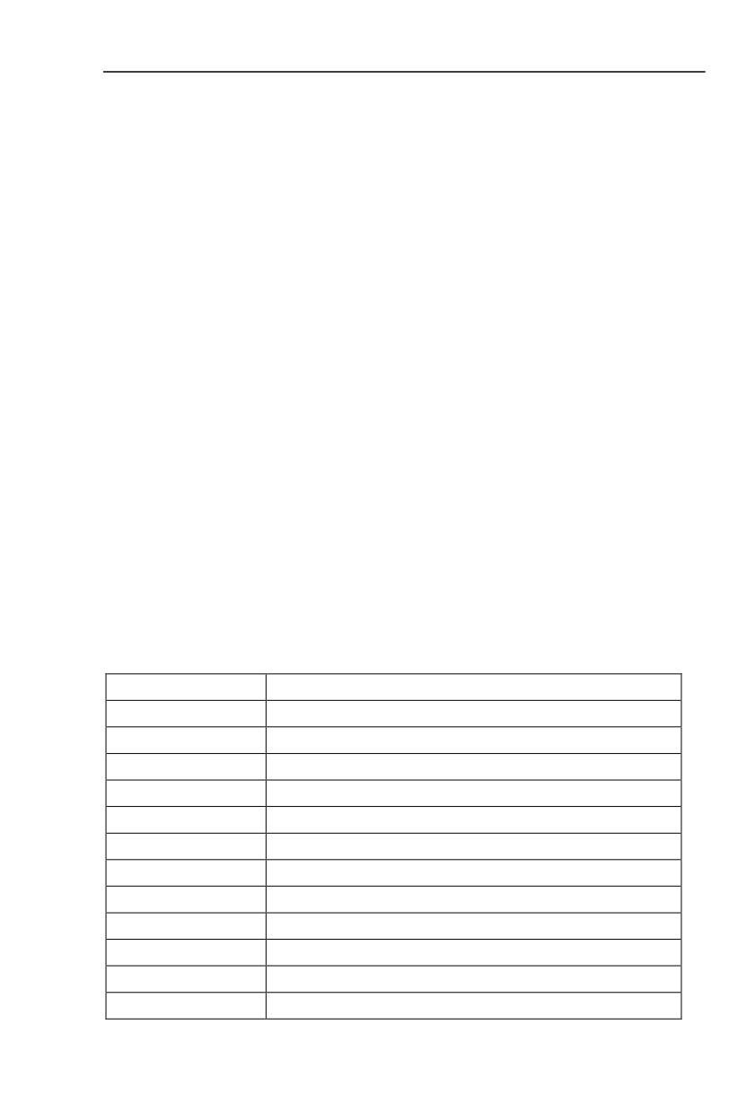
Stop/running parameter:
Parameter addr.
Parameter description
1000
* Communication setup value(-10000~10000)(Decimal)
1001
Running frequency
1002
Bus voltage
1003
Output voltage
1004
Output current
1005
Output power
1006
Output torque
1007
Running speed
1008
DI input status
1009
DO output status
100A
AI1voltage
100B
AI2 voltage
153
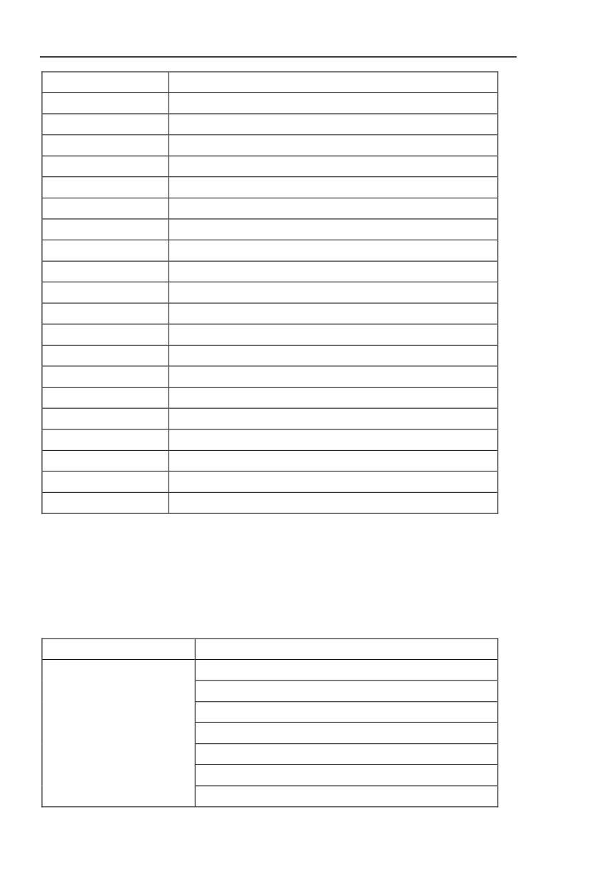
100C
AI3 voltage
100D
Counting value input
100E
Length value input
100F
Load speed
1010
PID setup
1011
PID feedback
1012
PLC process
1013
PULSE input pulse frequency, unit 0.01kHz
1014
Feedback speed, unit 0.1Hz
1015
Rest running time
1016
AI1 voltage before correction
1017
AI2 voltage before correction
1018
AI3 voltage before correction
1019
Line speed
101A
Current power on time
101B
Current running time
101C
PULSE input pulse frequency, unit 1Hz
101D
Communication setup value
101E
Actual feedback speed
101F
Main frequency X display
1020
Auxiliary frequency Y display
Caution:
The communication setup value is percentage of the relative value, 10000 corresponds
to
100.00% , -10000 correspondsto
-100.00%.For data of dimensional frequency,the
percentage value is the percentage of the maximum frequency.For data of dimensional
torque, the percentage is P2.10, A2.48, A3.48, A4.48
(Torque upper digital setup,
corresponding to the first, second, third, fourth motor).
Control command input to the inverter (write-only)
Command word address
Command function
0001:Forward operation
0002:Reverse operation
0003:Forward jog
2000
0004:Reverse jog
0005:Free stop
0006:Speed-Down stop
0007:Fault reset
154
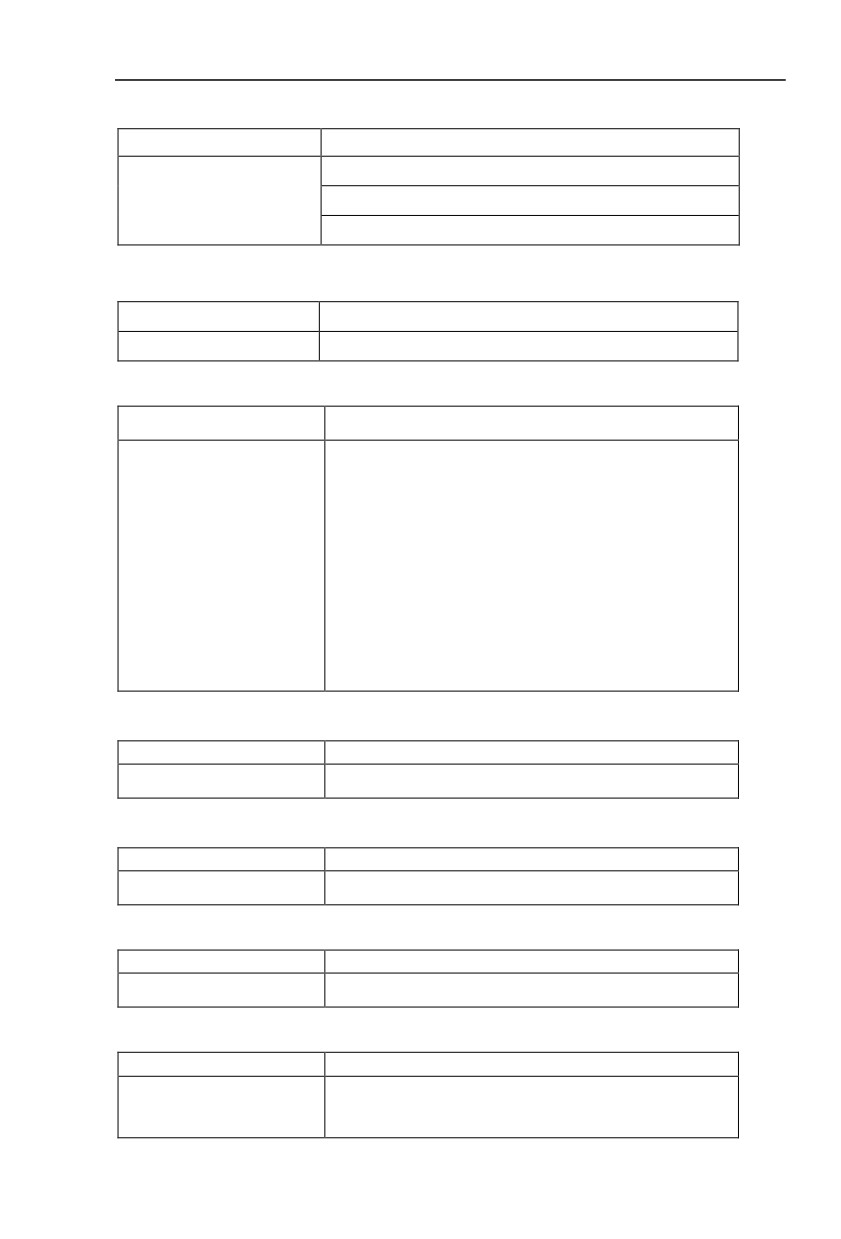
Read inverter status:(read-only)
Status word address
Status word function
0001:Forward operation
3000
0002:Reverse operation
0003:Stop
Parameters lock password check:(if the return is the 8888H, it indicates the password
checksum pass)
Password address
Contents of input password
1F00
*****
Digital output terminal control:(write-only)
Command address
Command content
BIT0:DO1 Output control
BIT1:DO2 Output control
BIT2 RELAY1 Output control
BIT3:RELAY2 Output control
BIT4:Y1R Output control
2001
BIT5:VY1
BIT6:VY2
BIT7:VY3
BIT8:VY4
BIT9:VY5
Analog output AO1 control:(write-only)
Command address
Command content
2002
0~7FFF indicates 0%~100%
Analog output AO2control:(write-only)
Command address
Command content
2003
0~7FFFindicates 0%~100%
(PULSE)output control :(write-only)
Command address
Command content
2004
0~7FFFindicates 0%~100%
Inverter fault description:
Inverter fault address
Inverter fault information
0000:No fault
8000
0001:Reserved
0002:Speed-up over current
155
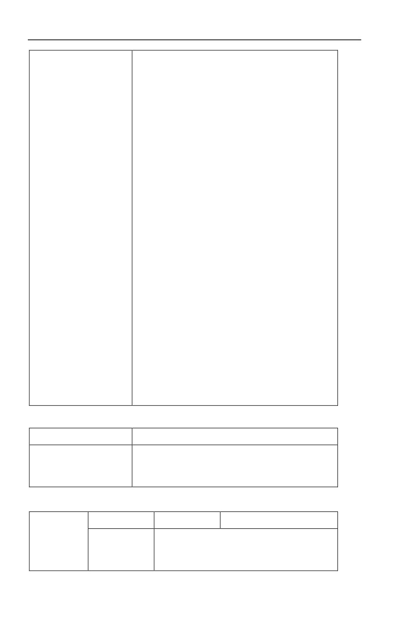
0003:Speed-down over current
0004:Constant speed over current
0005:Speed-up over voltage
0006:Speed-DOWN over voltage
0007:Constant speed over voltage
0008:Buffer resistance overload fault
0009:Under-voltage fault
000A:Inverter overload
000B:Motor overload
000C:Input phase lost
000D:Output phase lost
000E:Module overheating
000F:External fault
0010:Communication fault
0011:Contactor fault
0012:Current detection fault
0013:Motor tuning fault
0014:Encoder/PG card fault
0015:Parameter read and write fault
0016:Inverter hardware fault
0017:Motor earthing short-circuit fault
0018:Reserved
0019:Reserved
001A:Running time arrive fault
001B:User defined fault 1
001C:User defined fault 2
001D:Power on time arrive fault
001E:Load off
001F:PID feedback lost during operation
0028:Fast current limit timeout fault
0029:Motor shifting fault during operation
002A:Excessive speed deviation
002B:Motor over speed
002D:Motor over-temperature
005A:Encoder line number setup fault
005B:Encoder not connected
005C:Initial position error
005E:Speed feedback fault
Communication fault information describing data (fault code):
Communication fault address
Fault function description
0000:No fault
0001:Password error
0002:Command code error
0003:CRC check error
8001
0004:Invalid address
0005:Invalid parameter
0006:Parameter change invalid
0007:The system is locked
0008:Operating EEPROM
Pd group communication parameters description
Baud rate
Factory default value
6005
1 bit:MODUBS baud rate
Pd.00
0:300BPS
1:600BPS
Setup range
2:1200BPS
3:2400BPS
4:4800BPS
5:9600BPS
6:19200BPS
7:38400BPS
156