Intel 64 and IA-32 Architectures. Software Developer’s Manual (Collection, 2023) - page 42
CONTENTS
PAGE
Figure 34-1.
An Enclave Within the Application’s Virtual Address Space
34-1
Figure 36-1.
Enclave Memory Layout
36-1
Figure 36-2.
Measurement Flow of Enclave Build Process
36-7
Figure 36-3.
SGX Local Attestation
36-9
Figure 37-1.
Exit Stack Just After Interrupt with Stack Switch
37-1
Figure 37-2.
The SSA Stack
37-2
Figure 38-1.
Relationships Between SECS, SIGSTRUCT, and EINITTOKEN
38-47
Figure 40-1.
Single Stepping with Opt-out Entry - No AEX
40-2
Figure 40-2.
Single Stepping with Opt-out Entry -AEX Due to Non-SMI Event Before Single-Step Boundary
40-3
Figure 40-3.
LBR Stack Interaction with Opt-in Entry
40-6
Figure 40-4.
LBR Stack Interaction with Opt-out Entry
40-7
Vol. 3A xli
CONTENTS
PAGE
TABLES
Table 2-1.
IA32_EFER MSR Information
2-9
Table 2-2.
Action Taken By x87 FPU Instructions for Different Combinations of EM, MP, and TS
2-16
Table 2-3.
Summary of System Instructions
2-23
Table 3-1.
Code- and Data-Segment Types
3-12
Table 3-2.
System-Segment and Gate-Descriptor Types
3-14
Table 4-1.
Properties of Different Paging Modes
4-2
Table 4-2.
Paging Structures in the Different Paging Modes
4-8
Table 4-3.
Use of CR3 with 32-Bit Paging
4-12
Table 4-4.
Format of a 32-Bit Page-Directory Entry that Maps a 4-MByte Page
4-12
Table 4-6.
Format of a 32-Bit Page-Table Entry that Maps a 4-KByte Page
4-13
Table 4-5.
Format of a 32-Bit Page-Directory Entry that References a Page Table
4-13
Table 4-7.
Use of CR3 with PAE Paging
4-14
Table 4-8.
Format of a PAE Page-Directory-Pointer-Table Entry (PDPTE)
4-15
Table 4-9.
Format of a PAE Page-Directory Entry that Maps a 2-MByte Page
4-17
Table 4-10.
Format of a PAE Page-Directory Entry that References a Page Table
4-18
Table 4-11.
Format of a PAE Page-Table Entry that Maps a 4-KByte Page
4-18
Table 4-12.
Use of CR3 with 4-Level Paging and 5-level Paging and CR4.PCIDE = 0
4-20
Table 4-13.
Use of CR3 with 4-Level Paging and 5-Level Paging and CR4.PCIDE = 1
4-21
Table 4-14.
Format of a PML5 Entry (PML5E) that References a PML4 Table
4-26
Table 4-15.
Format of a PML4 Entry (PML4E) that References a Page-Directory-Pointer Table
4-26
Table 4-16.
Format of a Page-Directory-Pointer-Table Entry (PDPTE) that Maps a 1-GByte Page
4-27
Table 4-17.
Format of a Page-Directory-Pointer-Table Entry (PDPTE) that References a Page Directory
4-28
Table 4-18.
Format of a Page-Directory Entry that Maps a 2-MByte Page
4-29
Table 4-19.
Format of a Page-Directory Entry that References a Page Table
4-30
Table 4-20.
Format of a Page-Table Entry that Maps a 4-KByte Page
4-31
Table 5-1.
Privilege Check Rules for Call Gates
5-16
Table 5-2.
64-Bit-Mode Stack Layout After Far CALL with CPL Change
5-19
Table 5-3.
Combined Page-Directory and Page-Table Protection
5-29
Table 5-4.
Extended Feature Enable MSR (IA32_EFER)
5-30
Table 5-6.
4-KByte Page Level Protection Matrix with Execute-Disable Bit Capability with PAE Paging
5-31
Table 5-7.
2-MByte Page Level Protection with Execute-Disable Bit Capability with PAE Paging
5-31
Table 5-5.
Page Level Protection Matrix with Execute-Disable Bit Capability with 4-Level Paging
5-31
Table 5-9.
Reserved Bit Checking with Execute-Disable Bit Capability Not Enabled
5-32
Table 5-8.
Page Level Protection Matrix with Execute-Disable Bit Capability Enabled
5-32
Table 6-1.
Protected-Mode Exceptions and Interrupts
6-2
Table 6-2.
Priority Among Concurrent Events
6-8
Table 6-3.
Debug Exception Conditions and Corresponding Exception Classes
6-25
Table 6-4.
Interrupt and Exception Classes
6-33
Table 6-5.
Conditions for Generating a Double Fault
6-34
Table 6-6.
Invalid TSS Conditions
6-36
Table 6-7.
Alignment Requirements by Data Type
6-50
Table 6-8.
SIMD Floating-Point Exceptions Priority
6-54
Table 7-1.
Format of User Posted-Interrupt Descriptor - UPID
7-5
Table 8-1.
Exception Conditions Checked During a Task Switch
8-13
Table 8-2.
Effect of a Task Switch on Busy Flag, NT Flag, Previous Task Link Field, and TS Flag
8-15
Table 9-1.
Broadcast INIT-SIPI-SIPI Sequence and Choice of Timeouts
9-23
Table 9-2.
Initial APIC IDs for the Logical Processors in a System that has Four Intel Xeon MP Processors Supporting Intel
Hyper-Threading Technology1
9-39
Table 9-3.
Initial APIC IDs for the Logical Processors in a System that has Two Physical Processors Supporting Dual-Core and
Intel Hyper-Threading Technology
9-40
Table 9-4.
Example of Possible x2APIC ID Assignment in a System that has Two Physical Processors Supporting x2APIC and
Intel Hyper-Threading Technology
9-40
Table 9-5.
Boot Phase IPI Message Format
9-55
Table 10-1.
IA-32 and Intel® 64 Processor States Following Power-up, Reset, or INIT
10-2
Table 10-2.
Variance of RESET Values in Selected Intel Architecture Processors
10-4
Table 10-3.
Recommended Settings of EM and MP Flags on IA-32 Processors
10-6
Table 10-4.
Software Emulation Settings of EM, MP, and NE Flags
10-7
Table 10-5.
Main Initialization Steps in STARTUP.ASM Source Listing
10-16
Table 10-6.
Relationship Between BLD Item and ASM Source File
10-27
Table 10-7.
Microcode Update Field Definitions
10-28
Table 10-8.
Microcode Update Format
10-30
Table 10-9.
Extended Processor Signature Table Header Structure
10-31
xlii Vol. 3A
CONTENTS
PAGE
Table 10-10.
Processor Signature Structure
10-31
Table 10-11.
Processor Flags
10-33
Table 10-12.
Microcode Update Signature
10-37
Table 10-13.
Microcode Update Functions
10-42
Table 10-14.
Parameters for the Presence Test
10-42
Table 10-15.
Parameters for the Write Update Data Function
10-43
Table 10-16.
Parameters for the Control Update Sub-function
10-47
Table 10-17.
Mnemonic Values
10-47
Table 10-18.
Parameters for the Read Microcode Update Data Function
10-47
Table 10-19.
Return Code Definitions
10-49
Table 11-1.
Local APIC Register Address Map
11-6
Table 11-2.
Local APIC Timer Modes
11-17
Table 11-3.
Valid Combinations for Pentium 4 and Intel Xeon Processors Local xAPIC Interrupt Command Register
11-21
Table 11-4.
Valid Combinations for the P6 Family Processor Local APIC Interrupt Command Register
11-22
Table 11-5.
x2APIC Operating Mode Configurations
11-37
Table 11-6.
Local APIC Register Address Map Supported by x2APIC
11-38
Table 11-7.
MSR/MMIO Interface of a Local x2APIC in Different Modes of Operation
11-40
Table 11-8.
EOI Message (14 Cycles)
11-47
Table 11-9.
Short Message (21 Cycles)
11-48
Table 11-10.
Non-Focused Lowest Priority Message (34 Cycles)
11-49
Table 11-11.
APIC Bus Status Cycles Interpretation
11-51
Table 12-1.
Characteristics of the Caches, TLBs, Store Buffer, and Write Combining Buffer in Intel 64 and IA-32 Processors . 12-2
Table 12-2.
Memory Types and Their Properties
12-6
Table 12-3.
Methods of Caching Available in Intel Core 2 Duo, Intel Atom, Intel Core Duo, Pentium M, Pentium 4, Intel Xeon, P6
Family, and Pentium Processors
12-7
Table 12-4.
MESI Cache Line States
12-9
Table 12-5.
Cache Operating Modes
12-12
Table 12-6.
Effective Page-Level Memory Type for Pentium Pro and Pentium II Processors
12-14
Table 12-7.
Effective Page-Level Memory Types for Pentium III and More Recent Processor Families
12-15
Table 12-8.
Memory Types That Can Be Encoded in MTRRs
12-21
Table 12-9.
Address Mapping for Fixed-Range MTRRs
12-24
Table 12-10.
Memory Types That Can Be Encoded With PAT
12-34
Table 12-11.
Selection of PAT Entries with PAT, PCD, and PWT Flags
12-35
Table 12-12.
Memory Type Setting of PAT Entries Following a Power-up or Reset
12-35
Table 13-1.
Action Taken By MMX Instructions for Different Combinations of EM, MP, and TS
13-1
Table 13-3.
Effect of the MMX, x87 FPU, and FXSAVE/FXRSTOR Instructions on the x87 FPU Tag Word
13-3
Table 13-2.
Effects of MMX Instructions on x87 FPU State
13-3
Table 14-1.
Action Taken for Combinations of OSFXSR, OSXMMEXCPT, SSE, SSE2, SSE3, EM, MP, and TS
14-3
Table 14-2.
Action Taken for Combinations of OSFXSR, SSSE3, SSE4, EM, and TS
14-4
Table 14-3.
CPUID.(EAX=0DH, ECX=1) EAX Bit Assignment
14-8
Table 15-1.
Architectural and Non-Architectural MSRs Related to HWP
15-6
Table 15-2.
IA32_HWP_CTL MSR Bit 0 Behavior
15-13
Table 15-3.
Architectural and non-Architecture MSRs Related to HDC
15-21
Table 15-4.
Hardware Feedback Interface Structure
15-25
Table 15-5.
Hardware Feedback Interface Global Header Structure
15-26
Table 15-6.
Hardware Feedback Interface Logical Processor Entry Structure
15-26
Table 15-7.
Intel® Thread Director Table Structure
15-27
Table 15-8.
Intel® Thread Director Global Header Structure
15-28
Table 15-9.
Intel® Thread Director Logical Processor Entry Structure
15-29
Table 15-10.
IA32_HW_FEEDBACK_CONFIG Control Options
15-32
Table 15-11.
On-Demand Clock Modulation Duty Cycle Field Encoding
15-40
Table 15-12.
RAPL MSR Interfaces and RAPL Domains
15-50
Table 16-1.
Bits 54:53 in IA32_MCi_STATUS MSRs when IA32_MCG_CAP[11] = 1 and UC = 0
16-7
Table 16-2.
Overwrite Rules for Enabled Errors
16-8
Table 16-3.
Address Mode in IA32_MCi_MISC[8:6]
16-10
Table 16-4.
Address Mode in IA32_MCi_MISC[8:6]
16-11
Table 16-5.
Extended Machine Check State MSRs in Processors Without Support for Intel® 64 Architecture
16-12
Table 16-6.
Extended Machine Check State MSRs In Processors With Support for Intel® 64 Architecture
16-12
Table 16-7.
MC Error Classifications
16-18
Table 16-8.
Overwrite Rules for UC, CE, and UCR Errors
16-18
Table 16-9.
IA32_MCi_Status [15:0] Simple Error Code Encoding
16-21
Table 16-10.
IA32_MCi_Status [15:0] Compound Error Code Encoding
16-21
Table 16-11.
Encoding for TT (Transaction Type) Sub-Field
16-22
Table 16-12.
Level Encoding for LL (Memory Hierarchy Level) Sub-Field
16-22
Table 16-13.
Encoding of Request (RRRR) Sub-Field
16-23
Vol. 3A xliii
CONTENTS
PAGE
Table 16-14.
Encodings of PP, T, and II Sub-Fields
16-23
Table 16-15.
Encodings of MMM and CCCC Sub-Fields
16-24
Table 16-16.
MCA Compound Error Code Encoding for SRAO Errors
16-24
Table 16-17.
IA32_MCi_STATUS Values for SRAO Errors
16-25
Table 16-18.
IA32_MCG_STATUS Flag Indication for SRAO Errors
16-25
Table 16-19.
MCA Compound Error Code Encoding for SRAR Errors
16-25
Table 16-20.
IA32_MCi_STATUS Values for SRAR Errors
16-26
Table 16-21.
IA32_MCG_STATUS Flag Indication for SRAR Errors
16-26
Table 17-1.
CPUID DisplayFamily_DisplayModel Signatures for Processor Family 06H
17-1
Table 17-2.
Incremental Decoding Information: Processor Family 06H Machine Error Codes for Machine Check
17-1
Table 17-3.
CPUID DisplayFamily_DisplayModel Signatures for Processors Based on Intel® Core™ Microarchitecture
17-3
Table 17-4.
Incremental Bus Error Codes of Machine Check for Processors Based on Intel® Core™ Microarchitecture
17-4
Table 17-5.
Incremental MCA Error Code Types for Intel® Xeon® Processor 7400
17-6
Table 17-6.
Type B: Bus and Interconnect Error Codes
17-6
Table 17-7.
Type C: Cache Bus Controller Error Codes
17-7
Table 17-8.
Intel® QPI Machine Check Error Codes for IA32_MC0_STATUS and IA32_MC1_STATUS
17-8
Table 17-9.
Intel® QPI Machine Check Error Codes for IA32_MC0_MISC and IA32_MC1_MISC
17-8
Table 17-10.
Machine Check Error Codes for IA32_MC7_STATUS
17-9
Table 17-11.
Incremental Memory Controller Error Codes of Machine Check for IA32_MC8_STATUS
17-9
Table 17-12.
Incremental Memory Controller Error Codes of Machine Check for IA32_MC8_MISC
17-10
Table 17-13.
Machine Check Error Codes for IA32_MC4_STATUS
17-10
Table 17-14.
Intel® QPI MC Error Codes for IA32_MC6_STATUS and IA32_MC7_STATUS
17-11
Table 17-15.
Intel IMC MC Error Codes for IA32_MCi_STATUS (i= 8, 11)
17-12
Table 17-16.
Intel IMC MC Error Codes for IA32_MCi_MISC (i= 8, 11)
17-12
Table 17-17.
Machine Check Error Codes for IA32_MC4_STATUS
17-13
Table 17-18.
Intel IMC MC Error Codes for IA32_MCi_STATUS (i= 9-16)
17-14
Table 17-19.
Intel IMC MC Error Codes for IA32_MCi_MISC (i= 9-16)
17-15
Table 17-20.
Machine Check Error Codes for IA32_MC4_STATUS
17-16
Table 17-21.
Intel® QPI MC Error Codes for IA32_MCi_STATUS (i = 5, 20, 21)
17-17
Table 17-22.
Intel IMC MC Error Codes for IA32_MCi_STATUS (i= 9-16)
17-18
Table 17-23.
Intel IMC MC Error Codes for IA32_MCi_MISC (i= 9-16)
17-18
Table 17-24.
Machine Check Error Codes for IA32_MC4_STATUS
17-19
Table 17-25.
Intel IMC MC Error Codes for IA32_MCi_STATUS (i= 9-10)
17-20
Table 17-26.
Intel IMC MC Error Codes for IA32_MCi_STATUS (i= 9-16)
17-21
Table 17-27.
Intel HA MC Error Codes for IA32_MCi_MISC (i= 7, 8)
17-22
Table 17-28.
Machine Check Error Codes for IA32_MC4_STATUS
17-22
Table 17-29.
Interconnect MC Error Codes for IA32_MCi_STATUS (i = 5, 12, 19)
17-24
Table 17-30.
Intel IMC MC Error Codes for IA32_MCi_STATUS (i= 13-18)
17-26
Table 17-31.
M2M MC Error Codes for IA32_MCi_STATUS (i= 7, 8)
17-27
Table 17-32.
Intel HA MC Error Codes for IA32_MCi_MISC (i= 7, 8)
17-27
Table 17-33.
Intel IMC MC Error Codes for IA32_MCi_STATUS (i= 6, 7)
17-28
Table 17-34.
Machine Check Error Codes for IA32_MC4_STATUS
17-29
Table 17-35.
Interconnect MC Error Codes for IA32_MCi_STATUS (i = 5, 7, 8)
17-31
Table 17-36.
MSRs Reporting MC Error Codes by CPUID DisplayFamily_DisplaySignature
17-32
Table 17-37.
Intel IMC MC Error Codes for IA32_MCi_STATUS (i= 13-14, 17-18, 21-22, 25-26)
17-33
Table 17-38.
Additional Information Reported in IA32_MCi_MISC (i= 13-14, 17-18, 21-22, 25-26)
17-35
Table 17-39.
M2M MC Error Codes for IA32_MCi_STATUS (i= 12, 16, 20, 24)
17-36
Table 17-40.
Machine Check Error Codes for IA32_MC4_STATUS
17-37
Table 17-41.
Interconnect MC Error Codes for IA32_MC5_STATUS
17-40
Table 17-42.
Intel IMC MC Error Codes for IA32_MCi_STATUS (i= 13-20)
17-41
Table 17-43.
Additional Information Reported in IA32_MCi_MISC (i= 13-20)
17-43
Table 17-44.
M2M MC Error Codes for IA32_MC12_STATUS
17-44
Table 17-45.
Incremental Decoding Information: Processor Family 0FH, Machine Error Codes for Machine Check
17-45
Table 17-46.
MCi_STATUS Register Bit Definition
17-46
Table 17-47.
Incremental MCA Error Code for Intel® Xeon® Processor MP 7100
17-47
Table 17-48.
Other Information Field Bit Definition
17-47
Table 17-49.
Type A: L3 Error Codes
17-48
Table 17-50.
Type B: Bus and Interconnect Error Codes
17-48
Table 17-51.
Type C: Cache Bus Controller Error Codes
17-49
Table 17-52.
Decoding Family 0FH Machine Check Codes for Cache Hierarchy Errors
17-50
Table 18-1.
Breakpoint Examples
18-6
Table 18-2.
Debug Exception Conditions
18-9
Table 18-4.
LBR Stack Size and TOS Pointer Range
18-17
Table 18-3.
Legacy and Streamlined Operation with Freeze_Perfmon_On_PMI = 1, Counter Overflowed
18-17
Table 18-5.
IA32_DEBUGCTL Flag Encodings
18-25
xliv Vol. 3A
CONTENTS
PAGE
Table 18-6.
CPL-Qualified Branch Trace Store Encodings
18-26
Table 18-7.
MSR_LASTBRANCH_x_TO_IP for the Goldmont Microarchitecture
18-28
Table 18-8.
MSR_LASTBRANCH_x_FROM_IP
18-30
Table 18-9.
MSR_LASTBRANCH_x_TO_IP
18-31
Table 18-10.
LBR Stack Size and TOS Pointer Range
18-31
Table 18-11.
MSR_LBR_SELECT for Nehalem Microarchitecture
18-31
Table 18-12.
MSR_LBR_SELECT for Sandy Bridge Microarchitecture
18-32
Table 18-13.
MSR_LBR_SELECT for Haswell Microarchitecture
18-32
Table 18-14.
MSR_LASTBRANCH_x_FROM_IP with TSX Information
18-33
Table 18-15.
LBR Stack Size and TOS Pointer Range
18-34
Table 18-16.
MSR_LBR_INFO_x
18-34
Table 18-17.
LBR MSR Stack Size and TOS Pointer Range for the Pentium® 4 and the Intel® Xeon® Processor Family
18-37
Table 18-18.
Monitoring Supported Event IDs
18-49
Table 18-19.
Re-indexing of COS Numbers and Mapping to CAT/CDP Mask MSRs
18-63
Table 18-20.
MBA Delay Value MSRs
18-68
Table 19-1.
LBR IP Values for Various Operations
19-2
Table 19-2.
Branch Type Filtering Details
19-3
Table 19-3.
IA32_LBR_x_INFO and IA32_LER_INFO Branch Type Encodings
19-4
Table 19-4.
LBR VMCS Fields
19-5
Table 20-1.
UMask and Event Select Encodings for Pre-Defined Architectural Performance Events
20-5
Table 20-2.
Association of Fixed-Function Performance Counters with Architectural Performance Events
20-9
Table 20-3.
PEBS Record Format for Intel Core i7 Processor Family
20-20
Table 20-4.
Data Source Encoding for Load Latency Record
20-23
Table 20-5.
Off-Core Response Event Encoding
20-24
Table 20-6.
MSR_OFFCORE_RSP_0 and MSR_OFFCORE_RSP_1 Bit Field Definition
20-25
Table 20-7.
Opcode Field Encoding for MSR_UNCORE_ADDR_OPCODE_MATCH
20-30
Table 20-8.
Uncore PMU MSR Summary
20-32
Table 20-9.
Uncore PMU MSR Summary for Intel® Xeon® Processor E7 Family
20-33
Table 20-10.
Core PMU Comparison
20-34
Table 20-11.
PEBS Facility Comparison
20-37
Table 20-12.
PEBS Performance Events for Sandy Bridge Microarchitecture
20-38
Table 20-13.
Layout of Data Source Field of Load Latency Record
20-40
Table 20-15.
Off-Core Response Event Encoding
20-41
Table 20-14.
Layout of Precise Store Information In PEBS Record
20-41
Table 20-16.
MSR_OFFCORE_RSP_x Request_Type Field Definition
20-42
Table 20-17.
MSR_OFFCORE_RSP_x Response Supplier Info Field Definition
20-43
Table 20-18.
MSR_OFFCORE_RSP_x Snoop Info Field Definition
20-44
Table 20-19.
Uncore PMU MSR Summary
20-45
Table 20-20.
MSR_OFFCORE_RSP_x Supplier Info Field Definitions
20-46
Table 20-21.
Uncore PMU MSR Summary for Intel® Xeon® Processor E5 Family
20-47
Table 20-22.
Core PMU Comparison
20-48
Table 20-23.
PEBS Facility Comparison
20-48
Table 20-24.
PEBS Record Format for 4th Generation Intel Core Processor Family
20-49
Table 20-25.
Precise Events That Supports Data Linear Address Profiling
20-50
Table 20-26.
Layout of Data Linear Address Information In PEBS Record
20-51
Table 20-27.
MSR_OFFCORE_RSP_x Request_Type Definition (Haswell Microarchitecture)
20-51
Table 20-28.
MSR_OFFCORE_RSP_x Supplier Info Field Definition (CPUID Signatures: 06_3CH, 06_46H)
20-52
Table 20-29.
MSR_OFFCORE_RSP_x Supplier Info Field Definition (CPUID Signature: 06_45H)
20-52
Table 20-30.
MSR_OFFCORE_RSP_x Supplier Info Field Definition
20-53
Table 20-31.
TX Abort Information Field Definition
20-55
Table 20-32.
Uncore PMU MSR Summary
20-55
Table 20-33.
Core PMU Comparison
20-57
Table 20-34.
PEBS Facility Comparison
20-58
Table 20-35.
PEBS Record Format for the 6th Generation, 7th Generation, and 8th Generation Intel Core Processor Families 20-59
Table 20-36.
Precise Events for the Skylake, Kaby Lake, and Coffee Lake Microarchitectures
20-60
Table 20-37.
Layout of Data Linear Address Information In PEBS Record
20-61
Table 20-38.
FrontEnd_Retired Sub-Event Encodings Supported by MSR_PEBS_FRONTEND.EVTSEL
20-62
Table 20-39.
MSR_PEBS_FRONTEND Layout
20-62
Table 20-40.
MSR_OFFCORE_RSP_x Request_Type Definition (Skylake, Kaby Lake, and Coffee Lake Microarchitectures)
20-63
Table 20-41.
MSR_OFFCORE_RSP_x Supplier Info Field Definition (CPUID Signatures: 06_4EH, 06_5EH, 06_8EH, 06_9EH) . . 20-63
Table 20-42.
MSR_OFFCORE_RSP_x Snoop Info Field Definition (CPUID Signatures: 06_4EH, 06_5EH, 06_8EH, 06_9E,
06_55H)
20-64
Table 20-44.
MSR_OFFCORE_RSP_x Supplier Info Field Definition (CPUID Signature: 06_55H)
20-65
Table 20-43.
MSR_OFFCORE_RSP_x Request_Type Definition (Intel® Xeon® Scalable Processor Family)
20-65
Table 20-45.
MSR_OFFCORE_RSP_x Supplier Info Field Definition (CPUID Signature: 06_55H, Steppings 0x5H - 0xFH)
20-66
Vol. 3A xlv
CONTENTS
PAGE
Table 20-47.
MSR_OFFCORE_RSP_x Request_Type Definition (Processors Based on Ice Lake Microarchitecture)
20-67
Table 20-46.
Core PMU Summary of the Ice Lake Microarchitecture
20-67
Table 20-48.
MSR_OFFCORE_RSP_x Supplier Info Field Definition (Processors Based on Ice Lake Microarchitecture)
20-68
Table 20-49.
MSR_OFFCORE_RSP_x Snoop Info Field Definition (Processors Based on Ice Lake Microarchitecture)
20-69
Table 20-50.
Core PMU Summary of the Golden Cove Microarchitecture
20-71
Table 20-51.
Special Performance Monitoring Events with Counter Restrictions
20-72
Table 20-52.
Core PMU Summary of the Gracemont Microarchitecture
20-73
Table 20-53.
E-core PEBS Memory Access Info Encoding
20-73
Table 20-54.
E-core PEBS Data Source Encodings
20-74
Table 20-55.
MSR_OFFCORE_RSPx Request Type Definition
20-75
Table 20-56.
PEBS Performance Events for Knights Landing Microarchitecture
20-77
Table 20-57.
PEBS Record Format for Knights Landing Microarchitecture
20-77
Table 20-58.
OffCore Response Event Encoding
20-78
Table 20-59.
Bit fields of the MSR_OFFCORE_RESP [0, 1] Registers
20-78
Table 20-60.
PEBS Performance Events for the Silvermont Microarchitecture
20-81
Table 20-62.
OffCore Response Event Encoding
20-82
Table 20-61.
PEBS Record Format for the Silvermont Microarchitecture
20-82
Table 20-63.
MSR_OFFCORE_RSPx Request_Type Field Definition
20-83
Table 20-64.
MSR_OFFCORE_RSP_x Response Supplier Info Field Definition
20-84
Table 20-65.
MSR_OFFCORE_RSPx Snoop Info Field Definition
20-84
Table 20-66.
Core PMU Comparison Between the Goldmont and Silvermont Microarchitectures
20-85
Table 20-67.
Precise Events Supported by the Goldmont Microarchitecture
20-87
Table 20-68.
PEBS Record Format for the Goldmont Microarchitecture
20-88
Table 20-69.
MSR_OFFCORE_RSPx Request_Type Field Definition
20-89
Table 20-70.
MSR_OFFCORE_RSPx For L2 Miss and Outstanding Requests
20-90
Table 20-71.
Core PMU Comparison Between the Goldmont Plus and Goldmont Microarchitectures
20-91
Table 20-72.
Core PMU Comparison Between the Tremont and Goldmont Plus Microarchitectures
20-92
Table 20-73.
New Fields in IA32_PEBS_ENABLE
20-93
Table 20-74.
MSR_OFFCORE_RSPx Request Type Definition
20-94
Table 20-75.
MSR_OFFCORE_RSPx Response Type Definition
20-95
Table 20-76.
MSR_OFFCORE_RSPx Snoop Info Definition
20-95
Table 20-77.
Core Specificity Encoding within a Non-Architectural Umask
20-96
Table 20-78.
Agent Specificity Encoding within a Non-Architectural Umask
20-97
Table 20-79.
HW Prefetch Qualification Encoding within a Non-Architectural Umask
20-97
Table 20-80.
MESI Qualification Definitions within a Non-Architectural Umask
20-97
Table 20-81.
Bus Snoop Qualification Definitions within a Non-Architectural Umask
20-98
Table 20-82.
Snoop Type Qualification Definitions within a Non-Architectural Umask
20-98
Table 20-83.
At-Retirement Performance Events for Intel Core Microarchitecture
20-101
Table 20-84.
PEBS Performance Events for Intel Core Microarchitecture
20-102
Table 20-85.
Requirements to Program PEBS
20-103
Table 20-86.
Performance Counter MSRs and Associated CCCR and ESCR MSRs (Processors Based on Intel NetBurst
Microarchitecture)
20-104
Table 20-87.
Event Example
20-111
Table 20-88.
CCR Names and Bit Positions
20-115
Table 20-89.
Effect of Logical Processor and CPL Qualification for Logical-Processor-Specific (TS) Events
20-123
Table 20-90.
Effect of Logical Processor and CPL Qualification for Non-logical-Processor-specific (TI) Events
20-124
Table 20-91.
Nominal Core Crystal Clock Frequency
20-140
Table 20-92.
Basic Info Group
20-146
Table 20-93.
Memory Access Info Group
20-147
Table 20-94.
Updated Memory Access Info Group
20-148
Table 20-95.
GPRs in Ice Lake Microarchitecture
20-149
Table 20-96.
XMMs
20-149
Table 20-97.
LBRs
20-150
Table 20-98.
MSR_PEBS_CFG Programming
20-151
Table 20-99.
PEBS Record Example 1
20-151
Table 20-100.
PEBS Record Example 2
20-152
Table 20-101.
Data Source Encoding for Memory Accesses (Ice Lake and Later Microarchitectures)
20-155
Table 21-1.
Real-Address Mode Exceptions and Interrupts
21-6
Table 21-2.
Software Interrupt Handling Methods While in Virtual-8086 Mode
21-17
Table 22-1.
Characteristics of 16-Bit and 32-Bit Program Modules
22-1
Table 23-1.
New Instruction in the Pentium Processor and Later IA-32 Processors
23-4
Table 23-3.
EM and MP Flag Interpretation
23-17
Table 23-2.
Recommended Values of the EM, MP, and NE Flags for Intel486 SX Microprocessor/Intel 487 SX Math
Coprocessor System
23-17
Table 23-4.
Exception Conditions for Legacy SIMD/MMX Instructions with FP Exception and 16-Byte Alignment
23-22
xlvi Vol. 3A
CONTENTS
PAGE
Table 23-5.
Exception Conditions for Legacy SIMD/MMX Instructions with XMM and FP Exception
23-23
Table 23-6.
Exception Conditions for Legacy SIMD/MMX Instructions with XMM and without FP Exception
23-24
Table 23-7.
Exception Conditions for SIMD/MMX Instructions with Memory Reference
23-25
Table 23-8.
Exception Conditions for Legacy SIMD/MMX Instructions without FP Exception
23-26
Table 23-9.
Exception Conditions for Legacy SIMD/MMX Instructions without Memory Reference
23-27
Table 23-10.
Processor State Following Power-up/Reset/INIT for Pentium, Pentium Pro and Pentium 4 Processors
23-37
Table 25-1.
Format of the VMCS Region
25-2
Table 25-2.
Format of Access Rights
25-4
Table 25-3.
Format of Interruptibility State
25-6
Table 25-4.
Format of Pending-Debug-Exceptions
25-7
Table 25-5.
Definitions of Pin-Based VM-Execution Controls
25-10
Table 25-6.
Definitions of Primary Processor-Based VM-Execution Controls
25-10
Table 25-7.
Definitions of Secondary Processor-Based VM-Execution Controls
25-12
Table 25-8.
Definitions of Tertiary Processor-Based VM-Execution Controls
25-13
Table 25-9.
Format of Extended-Page-Table Pointer
25-17
Table 25-10.
Definitions of VM-Function Controls
25-18
Table 25-11.
Format of Sub-Page-Permission-Table Pointer
25-19
Table 25-12.
Format of Hypervisor-Managed Linear-Address Translation Pointer
25-20
Table 25-13.
Definitions of Primary VM-Exit Controls
25-21
Table 25-14.
Definitions of Secondary VM-Exit Controls
25-22
Table 25-15.
Format of an MSR Entry
25-23
Table 25-16.
Definitions of VM-Entry Controls
25-23
Table 25-17.
Format of the VM-Entry Interruption-Information Field
25-25
Table 25-18.
Format of Exit Reason
25-26
Table 25-19.
Format of the VM-Exit Interruption-Information Field
25-27
Table 25-20.
Format of the IDT-Vectoring Information Field
25-28
Table 25-21.
Structure of VMCS Component Encoding
25-30
Table 26-1.
Format of the Virtualization-Exception Information Area
26-21
Table 28-1.
Exit Qualification for Debug Exceptions
28-4
Table 28-2.
Exit Qualification for Task Switches
28-5
Table 28-3.
Exit Qualification for Control-Register Accesses
28-7
Table 28-4.
Exit Qualification for MOV DR
28-8
Table 28-5.
Exit Qualification for I/O Instructions
28-8
Table 28-6.
Exit Qualification for APIC-Access VM Exits from Linear Accesses and Guest-Physical Accesses
28-9
Table 28-7.
Exit Qualification for EPT Violations
28-10
Table 28-8.
Format of the VM-Exit Instruction-Information Field as Used for INS and OUTS
28-16
Table 28-9.
Format of the VM-Exit Instruction-Information Field as Used for INVEPT, INVPCID, and INVVPID
28-17
Table 28-10.
Format of the VM-Exit Instruction-Information Field as Used for LIDT, LGDT, SIDT, or SGDT
28-18
Table 28-11.
Format of the VM-Exit Instruction-Information Field as Used for LLDT, LTR, SLDT, and STR
28-19
Table 28-12.
Format of the VM-Exit Instruction-Information Field as Used for RDRAND and RDSEED
28-20
Table 28-13.
Format of the VM-Exit Instruction-Information Field as Used for TPAUSE and UMWAIT
28-20
Table 28-14.
Format of the VM-Exit Instruction-Information Field as Used for VMCLEAR, VMPTRLD, VMPTRST, VMXON,
XRSTORS, and XSAVES
28-21
Table 28-15.
Format of the VM-Exit Instruction-Information Field as Used for VMREAD and VMWRITE
28-22
Table 28-16.
Format of the VM-Exit Instruction-Information Field as Used for LOADIWKEY
28-23
Table 29-1.
Format of an EPT PML5 Entry (PML5E) that References an EPT PML4 Table
29-4
Table 29-2.
Format of an EPT PML4 Entry (PML4E) that References an EPT Page-Directory-Pointer Table
29-5
Table 29-3.
Format of an EPT Page-Directory-Pointer-Table Entry (PDPTE) that Maps a 1-GByte Page
29-6
Table 29-4.
Format of an EPT Page-Directory-Pointer-Table Entry (PDPTE) that References an EPT Page Directory
29-7
Table 29-5.
Format of an EPT Page-Directory Entry (PDE) that Maps a 2-MByte Page
29-8
Table 29-6.
Format of an EPT Page-Directory Entry (PDE) that References an EPT Page Table
29-9
Table 29-7.
Format of an EPT Page-Table Entry that Maps a 4-KByte Page
29-11
Table 30-1.
Format of Posted-Interrupt Descriptor
30-15
Table 31-1.
VM-Instruction Error Numbers
31-31
Table 32-1.
SMRAM State Save Map
32-5
Table 32-2.
Processor Signatures and 64-bit SMRAM State Save Map Format
32-6
Table 32-3.
SMRAM State Save Map for Intel 64 Architecture
32-7
Table 32-4.
Processor Register Initialization in SMM
32-9
Table 32-5.
I/O Instruction Information in the SMM State Save Map
32-12
Table 32-6.
I/O Instruction Type Encodings
32-12
Table 32-7.
Auto HALT Restart Flag Values
32-14
Table 32-8.
I/O Instruction Restart Field Values
32-16
Table 32-9.
Exit Qualification for SMIs That Arrive Immediately After the Retirement of an I/O Instruction
32-21
Table 32-10.
Format of MSEG Header
32-25
Table 33-1.
COFI Type for Branch Instructions
33-3
Vol. 3A xlvii
CONTENTS
PAGE
Table 33-2.
IP Filtering Packet Example
33-7
Table 33-3.
ToPA Table Entry Fields
33-12
Table 33-4.
Algorithm to Manage Intel PT ToPA PMI and XSAVES/XRSTORS
33-15
Table 33-5.
Behavior on Restricted Memory Access
33-16
Table 33-6.
IA32_RTIT_CTL MSR
33-17
Table 33-7.
IA32_RTIT_STATUS MSR
33-21
Table 33-8.
IA32_RTIT_OUTPUT_BASE MSR
33-23
Table 33-10.
TSX Packet Scenarios with BranchEn=1
33-24
Table 33-9.
IA32_RTIT_OUTPUT_MASK_PTRS MSR
33-24
Table 33-11.
CPUID Leaf 14H Enumeration of Intel Processor Trace Capabilities
33-27
Table 33-12.
CPUID Leaf 14H, sub-leaf 1H Enumeration of Intel Processor Trace Capabilities
33-29
Table 33-13.
An Illustrative CYC Packet Example
33-34
Table 33-14.
Compound Packet Event Summary
33-37
Table 33-15.
Packets Forbidden Between BBP and BEP
33-37
Table 33-16.
TNT Packet Definition
33-39
Table 33-17.
IP Packet Definition
33-40
Table 33-18.
FUP/TIP IP Reconstruction
33-41
Table 33-19.
TNT Examples with Deferred TIPs
33-42
Table 33-20.
TIP.PGE Packet Definition
33-43
Table 33-21.
TIP.PGD Packet Definition
33-44
Table 33-22.
FUP Packet Definition
33-45
Table 33-23.
FUP Cases and IP Payload
33-46
Table 33-24.
PIP Packet Definition
33-47
Table 33-25.
General Form of MODE Packets
33-48
Table 33-26.
MODE.Exec Packet Definition
33-48
Table 33-27.
MODE.TSX Packet Definition
33-49
Table 33-28.
TraceStop Packet Definition
33-50
Table 33-29.
CBR Packet Definition
33-50
Table 33-30.
TSC Packet Definition
33-51
Table 33-31.
MTC Packet Definition
33-52
Table 33-32.
TMA Packet Definition
33-53
Table 33-33.
Cycle Count Packet Definition
33-54
Table 33-34.
VMCS Packet Definition
33-55
Table 33-35.
OVF Packet Definition
33-56
Table 33-36.
PSB Packet Definition
33-56
Table 33-37.
PSBEND Packet Definition
33-57
Table 33-38.
MNT Packet Definition
33-58
Table 33-39.
PAD Packet Definition
33-58
Table 33-40.
PTW Packet Definition
33-59
Table 33-41.
EXSTOP Packet Definition
33-60
Table 33-42.
MWAIT Packet Definition
33-61
Table 33-43.
PWRE Packet Definition
33-62
Table 33-44.
PWRX Packet Definition
33-63
Table 33-45.
Block Begin Packet Definition
33-64
Table 33-46.
Block Item Packet Definition
33-65
Table 33-47.
BIP Encodings
33-65
Table 33-48.
Block End Packet Definition
33-70
Table 33-49.
Control Flow Event Packet Definition
33-71
Table 33-50.
CFE Packet Type and Vector Fields Details
33-71
Table 33-51.
Event Data Packet Definition
33-73
Table 33-52.
VMX Controls For Intel Processor Trace
33-74
Table 33-53.
Packets on VMX Transitions (System-Wide Tracing)
33-75
Table 33-54.
Packets on a Failed VM Entry
33-76
Table 33-55.
Packet Generation under Different Example Operations
33-77
Table 33-56.
Packet Generation with Operations That Alter the Value of PacketEn
33-78
Table 33-57.
Examples of PTWRITE when TriggerEn && PTWEn is True
33-79
Table 33-58.
Examples of Power Event Trace when TriggerEn && PwrEvtEn is True
33-79
Table 33-59.
Event Trace Examples when TriggerEn && ContextEn && EventEn is True
33-80
Table 34-1.
Supervisor and User Mode Enclave Instruction Leaf Functions in Long-Form of SGX1
34-3
Table 34-2.
Supervisor and User Mode Enclave Instruction Leaf Functions in Long-Form of SGX2
34-4
Table 34-3.
VMX Operation and Supervisor Mode Enclave Instruction Leaf Functions in Long-Form of OVERSUB
34-4
Table 34-4.
Intel® SGX Opt-in and Enabling Behavior
34-5
Table 34-5.
CPUID Leaf 12H, Sub-Leaf 0 Enumeration of Intel® SGX Capabilities
34-5
Table 34-6.
CPUID Leaf 12H, Sub-Leaf 1 Enumeration of Intel® SGX Capabilities
34-6
Table 34-7.
CPUID Leaf 12H, Sub-Leaf Index 2 or Higher Enumeration of Intel® SGX Resources
34-6
xlviii Vol. 3A
CONTENTS
PAGE
Table 35-1.
List of Implicit and Explicit Memory Access by Intel® SGX Enclave Instructions
35-3
Table 35-2.
Layout of SGX Enclave Control Structure (SECS)
35-5
Table 35-3.
Layout of ATTRIBUTES Structure
35-6
Table 35-4.
Bit Vector Layout of MISCSELECT Field of Extended Information
35-6
Table 35-5.
Bit Vector Layout of CET_ATTRIBUTES Field of Extended Information
35-7
Table 35-6.
Layout of Thread Control Structure (TCS)
35-7
Table 35-7.
Layout of TCS.FLAGS Field
35-8
Table 35-8.
Top-to-Bottom Layout of an SSA Frame
35-9
Table 35-9.
Layout of GPRSGX Portion of the State Save Area
35-9
Table 35-10.
Layout of EXITINFO Field
35-10
Table 35-11.
Exception Vectors
35-10
Table 35-12.
Layout of MISC region of the State Save Area
35-11
Table 35-13.
Layout of EXINFO Structure
35-11
Table 35-14.
Page Fault Error Code
35-12
Table 35-15.
Layout of CET State Save Area Frame
35-12
Table 35-16.
Layout of PAGEINFO Data Structure
35-12
Table 35-17.
Layout of SECINFO Data Structure
35-13
Table 35-18.
Layout of SECINFO.FLAGS Field
35-13
Table 35-19.
Supported PAGE_TYPE
35-13
Table 35-20.
Layout of PCMD Data Structure
35-14
Table 35-21.
Layout of Enclave Signature Structure (SIGSTRUCT)
35-14
Table 35-23.
Layout of REPORT
35-16
Table 35-22.
Layout of EINIT Token (EINITTOKEN)
35-16
Table 35-24.
Layout of TARGETINFO Data Structure
35-17
Table 35-25.
Layout of KEYREQUEST Data Structure
35-18
Table 35-26.
Supported KEYName Values
35-18
Table 35-27.
Layout of KEYPOLICY Field
35-18
Table 35-28.
Layout of Version Array Data Structure
35-19
Table 35-29.
Content of an Enclave Page Cache Map Entry
35-19
Table 35-30.
Layout of RDINFO Structure
35-20
Table 35-31.
Layout of RDINFO STATUS Structure
35-20
Table 35-32.
Layout of RDINFO FLAGS Structure
35-20
Table 36-1.
Illegal Instructions Inside an Enclave
36-15
Table 37-1.
GPR, x87 Synthetic States on Asynchronous Enclave Exit
37-3
Table 38-1.
Register Usage of Privileged Enclave Instruction Leaf Functions
38-1
Table 38-2.
Register Usage of Unprivileged Enclave Instruction Leaf Functions
38-2
Table 38-3.
Register Usage of Virtualization Operation Enclave Instruction Leaf Functions
38-2
Table 38-4.
Error or Information Codes for Intel® SGX Instructions
38-2
Table 38-5.
List of Internal CREG
38-3
Table 38-6.
Base Concurrency Restrictions
38-5
Table 38-7.
Additional Concurrency Restrictions
38-6
Table 38-8.
Base Concurrency Restrictions of EADD
38-17
Table 38-9.
Additional Concurrency Restrictions of EADD
38-18
Table 38-10.
Base Concurrency Restrictions of EAUG
38-22
Table 38-11.
Additional Concurrency Restrictions of EAUG
38-23
Table 38-12.
EBLOCK Return Value in RAX
38-27
Table 38-13.
Base Concurrency Restrictions of EBLOCK
38-27
Table 38-14.
Additional Concurrency Restrictions of EBLOCK
38-28
Table 38-15.
Base Concurrency Restrictions of ECREATE
38-30
Table 38-16.
Additional Concurrency Restrictions of ECREATE
38-31
Table 38-17.
EDBGRD Return Value in RAX
38-36
Table 38-18.
Base Concurrency Restrictions of EDBGRD
38-37
Table 38-19.
Additional Concurrency Restrictions of EDBGRD
38-37
Table 38-20.
EDBGWR Return Value in RAX
38-40
Table 38-21.
Base Concurrency Restrictions of EDBGWR
38-41
Table 38-22.
Additional Concurrency Restrictions of EDBGWR
38-41
Table 38-23.
Base Concurrency Restrictions of EEXTEND
38-44
Table 38-24.
Additional Concurrency Restrictions of EEXTEND
38-45
Table 38-25.
EINIT Return Value in RAX
38-48
Table 38-26.
Base Concurrency Restrictions of EINIT
38-49
Table 38-27.
Additional Concurrency Restrictions of ENIT
38-49
Table 38-28.
ELDB/ELDU/ELDBC/ELBUC Return Value in RAX
38-55
Table 38-29.
Base Concurrency Restrictions of ELDB/ELDU/ELDBC/ELBUC
38-56
Table 38-30.
Additional Concurrency Restrictions of ELDB/ELDU/ELDBC/ELBUC
38-56
Table 38-31.
EMODPR Return Value in RAX
38-61
Vol. 3A xlix
CONTENTS
PAGE
Table 38-32.
Base Concurrency Restrictions of EMODPR
38-61
Table 38-33.
Additional Concurrency Restrictions of EMODPR
38-62
Table 38-34.
EMODT Return Value in RAX
38-64
Table 38-35.
Base Concurrency Restrictions of EMODT
38-64
Table 38-36.
Additional Concurrency Restrictions of EMODT
38-65
Table 38-37.
Base Concurrency Restrictions of EPA
38-67
Table 38-38.
Additional Concurrency Restrictions of EPA
38-67
Table 38-39.
ERDINFO Return Value in RAX
38-69
Table 38-40.
Base Concurrency Restrictions of ERDINFO
38-70
Table 38-41.
Additional Concurrency Restrictions of ERDINFO
38-70
Table 38-42.
EREMOVE Return Value in RAX
38-73
Table 38-43.
Base Concurrency Restrictions of EREMOVE
38-74
Table 38-44.
Additional Concurrency Restrictions of EREMOVE
38-74
Table 38-45.
ETRACK Return Value in RAX
38-77
Table 38-46.
Base Concurrency Restrictions of ETRACK
38-77
Table 38-47.
Additional Concurrency Restrictions of ETRACK
38-77
Table 38-48.
ETRACKC Return Value in RAX
38-80
Table 38-49.
Base Concurrency Restrictions of ETRACKC
38-80
Table 38-50.
Additional Concurrency Restrictions of ETRACKC
38-81
Table 38-51.
EWB Return Value in RAX
38-84
Table 38-52.
Base Concurrency Restrictions of EWB
38-84
Table 38-53.
Additional Concurrency Restrictions of EWB
38-84
Table 38-54.
EACCEPT Return Value in RAX
38-90
Table 38-55.
Base Concurrency Restrictions of EACCEPT
38-91
Table 38-56.
Additional Concurrency Restrictions of EACCEPT
38-91
Table 38-57.
EACCEPTCOPY Return Value in RAX
38-95
Table 38-58.
Base Concurrency Restrictions of EACCEPTCOPY
38-96
Table 38-59.
Additional Concurrency Restrictions of EACCEPTCOPY
38-96
Table 38-60.
Base Concurrency Restrictions of EDECCSSA
38-99
Table 38-61.
Additional Concurrency Restrictions of EDECCSSA
38-99
Table 38-62.
Base Concurrency Restrictions of EENTER
38-104
Table 38-63.
Additional Concurrency Restrictions of EENTER
38-104
Table 38-64.
Base Concurrency Restrictions of EEXIT
38-112
Table 38-65.
Additional Concurrency Restrictions of EEXIT
38-112
Table 38-66.
Key Derivation
38-116
Table 38-67.
EGETKEY Return Value in RAX
38-116
Table 38-68.
Base Concurrency Restrictions of EGETKEY
38-116
Table 38-69.
Additional Concurrency Restrictions of EGETKEY
38-117
Table 38-70.
Base Concurrency Restrictions of EMODPE
38-125
Table 38-71.
Additional Concurrency Restrictions of EMODPE
38-125
Table 38-72.
Base Concurrency Restrictions of EREPORT
38-129
Table 38-73.
Additional Concurrency Restrictions of EREPORT
38-129
Table 38-74.
Base Concurrency Restrictions of ERESUME
38-134
Table 38-75.
Additional Concurrency Restrictions of ERESUME
38-134
Table 38-76.
Base Concurrency Restrictions of EDECVIRTCHILD
38-146
Table 38-77.
Additional Concurrency Restrictions of EDECVIRTCHILD
38-147
Table 38-78.
Base Concurrency Restrictions of EINCVIRTCHILD
38-150
Table 38-79.
Additional Concurrency Restrictions of EINCVIRTCHILD
38-151
Table 38-80.
Base Concurrency Restrictions of ESETCONTEXT
38-153
Table 38-81.
Additional Concurrency Restrictions of ESETCONTEXT
38-154
Table 39-1.
SGX Conflict Exit Qualification
39-4
Table 39-2.
SMRAM Synthetic States on Asynchronous Enclave Exit
39-11
Table 39-3.
Layout of the IA32_SGX_SVN_STATUS MSR
39-13
Table A-1.
Memory Types Recommended for VMCS and Related Data Structures
A-1
Table B-1.
Encoding for 16-Bit Control Fields (0000_00xx_xxxx_xxx0B)
B-1
Table B-2.
Encodings for 16-Bit Guest-State Fields (0000_10xx_xxxx_xxx0B)
B-1
Table B-3.
Encodings for 16-Bit Host-State Fields (0000_11xx_xxxx_xxx0B)
B-2
Table B-4.
Encodings for 64-Bit Control Fields (0010_00xx_xxxx_xxxAb)
B-2
Table B-5.
Encodings for 64-Bit Read-Only Data Field (0010_01xx_xxxx_xxxAb)
B-5
Table B-6.
Encodings for 64-Bit Guest-State Fields (0010_10xx_xxxx_xxxAb)
B-5
Table B-7.
Encodings for 64-Bit Host-State Fields (0010_11xx_xxxx_xxxAb)
B-6
Table B-8.
Encodings for 32-Bit Control Fields (0100_00xx_xxxx_xxx0B)
B-7
Table B-9.
Encodings for 32-Bit Read-Only Data Fields (0100_01xx_xxxx_xxx0B)
B-8
Table B-10.
Encodings for 32-Bit Guest-State Fields (0100_10xx_xxxx_xxx0B)
B-8
Table B-11.
Encoding for 32-Bit Host-State Field (0100_11xx_xxxx_xxx0B)
B-9
l Vol. 3A
CONTENTS
PAGE
Table B-12.
Encodings for Natural-Width Control Fields (0110_00xx_xxxx_xxx0B)
B-9
Table B-13.
Encodings for Natural-Width Read-Only Data Fields (0110_01xx_xxxx_xxx0B)
B-10
Table B-14.
Encodings for Natural-Width Guest-State Fields (0110_10xx_xxxx_xxx0B)
B-10
Table B-15.
Encodings for Natural-Width Host-State Fields (0110_11xx_xxxx_xxx0B)
B-11
Table C-1.
Basic Exit Reasons
C-1
Vol. 3A li
CONTENTS
PAGE
lii Vol. 3A
CHAPTER 1
ABOUT THIS MANUAL
The Intel® 64 and IA-32 Architectures Software Developer’s Manual, Volume 3A: System Programming Guide, Part
1 (order number 253668), the Intel® 64 and IA-32 Architectures Software Developer’s Manual, Volume 3B: System
Programming Guide, Part 2 (order number 253669), the Intel® 64 and IA-32 Architectures Software Developer’s
Manual, Volume 3C: System Programming Guide, Part 3 (order number 326019), and the Intel® 64 and IA-32
Architectures Software Developer’s Manual, Volume 3D:System Programming Guide, Part 4 (order number
332831) are part of a set that describes the architecture and programming environment of Intel 64 and IA-32
Architecture processors. The other volumes in this set are:
• Intel® 64 and IA-32 Architectures Software Developer’s Manual, Volume 1: Basic Architecture (order number
253665).
• Intel® 64 and IA-32 Architectures Software Developer’s Manual, Volumes 2A, 2B, 2C, & 2D: Instruction Set
Reference (order numbers 253666, 253667, 326018, and 334569).
• The Intel® 64 and IA-32 Architectures Software Developer’s Manual, Volume 4: Model-Specific Registers
(order number 335592).
The Intel® 64 and IA-32 Architectures Software Developer’s Manual, Volume 1, describes the basic architecture
and programming environment of Intel 64 and IA-32 processors. The Intel® 64 and IA-32 Architectures Software
Developer’s Manual, Volumes 2A, 2B, 2C, & 2D, describe the instruction set of the processor and the opcode struc-
ture. These volumes apply to application programmers and to programmers who write operating systems or exec-
utives. The Intel® 64 and IA-32 Architectures Software Developer’s Manual, Volumes 3A, 3B, 3C, & 3D, describe
the operating-system support environment of Intel 64 and IA-32 processors. These volumes target operating-
system and BIOS designers. In addition, Intel® 64 and IA-32 Architectures Software Developer’s Manual, Volume
3B, and Intel® 64 and IA-32 Architectures Software Developer’s Manual, Volume 3C, address the programming
environment for classes of software that host operating systems. The Intel® 64 and IA-32 Architectures Software
Developer’s Manual, Volume 4, describes the model-specific registers of Intel 64 and IA-32 processors.
1.1
INTEL® 64 AND IA-32 PROCESSORS COVERED IN THIS MANUAL
This manual set includes information pertaining primarily to the most recent Intel 64 and IA-32 processors, which
include:
• Pentium® processors
• P6 family processors
• Pentium® 4 processors
• Pentium® M processors
• Intel® Xeon® processors
• Pentium® D processors
• Pentium® processor Extreme Editions
•
64-bit Intel® Xeon® processors
• Intel® Core™ Duo processor
• Intel® Core™ Solo processor
• Dual-Core Intel® Xeon® processor LV
• Intel® Core™ 2 Duo processor
• Intel® Core™ 2 Quad processor Q6000 series
• Intel® Xeon® processor 3000, 3200 series
• Intel® Xeon® processor 5000 series
• Intel® Xeon® processor 5100, 5300 series
Vol. 3A
1-1
ABOUT THIS MANUAL
•
Intel® Core™ 2 Extreme processor X7000 and X6800 series
•
Intel® Core™ 2 Extreme QX6000 series
•
Intel® Xeon® processor 7100 series
•
Intel® Pentium® Dual-Core processor
•
Intel® Xeon® processor 7200, 7300 series
•
Intel® Core™ 2 Extreme QX9000 series
•
Intel® Xeon® processor 5200, 5400, 7400 series
•
Intel® Core™ 2 Extreme processor QX9000 and X9000 series
•
Intel® Core™ 2 Quad processor Q9000 series
•
Intel® Core™ 2 Duo processor E8000, T9000 series
•
Intel Atom® processors 200, 300, D400, D500, D2000, N200, N400, N2000, E2000, Z500, Z600, Z2000,
C1000 series are built from 45 nm and 32 nm processes.
•
Intel® Core™ i7 processor
•
Intel® Core™ i5 processor
•
Intel® Xeon® processor E7-8800/4800/2800 product families
•
Intel® Core™ i7-3930K processor
•
2nd generation Intel® Core™ i7-2xxx, Intel® Core™ i5-2xxx, Intel® Core™ i3-2xxx processor series
•
Intel® Xeon® processor E3-1200 product family
•
Intel® Xeon® processor E5-2400/1400 product family
•
Intel® Xeon® processor E5-4600/2600/1600 product family
•
3rd generation Intel® Core™ processors
•
Intel® Xeon® processor E3-1200 v2 product family
•
Intel® Xeon® processor E5-2400/1400 v2 product families
•
Intel® Xeon® processor E5-4600/2600/1600 v2 product families
•
Intel® Xeon® processor E7-8800/4800/2800 v2 product families
•
4th generation Intel® Core™ processors
•
The Intel® Core™ M processor family
•
Intel® Core™ i7-59xx Processor Extreme Edition
•
Intel® Core™ i7-49xx Processor Extreme Edition
•
Intel® Xeon® processor E3-1200 v3 product family
•
Intel® Xeon® processor E5-2600/1600 v3 product families
•
5th generation Intel® Core™ processors
•
Intel® Xeon® processor D-1500 product family
•
Intel® Xeon® processor E5 v4 family
•
Intel Atom® processor X7-Z8000 and X5-Z8000 series
•
Intel Atom® processor Z3400 series
•
Intel Atom® processor Z3500 series
•
6th generation Intel® Core™ processors
•
Intel® Xeon® processor E3-1500m v5 product family
•
7th generation Intel® Core™ processors
•
Intel® Xeon Phi™ Processor 3200, 5200, 7200 Series
•
Intel® Xeon® Scalable Processor Family
•
8th generation Intel® Core™ processors
•
Intel® Xeon Phi™ Processor 7215, 7285, 7295 Series
1-2
Vol. 3A
ABOUT THIS MANUAL
• Intel® Xeon® E processors
• 9th generation Intel® Core™ processors
• 2nd generation Intel® Xeon® Scalable Processor Family
•
10th generation Intel® Core™ processors
•
11th generation Intel® Core™ processors
• 3rd generation Intel® Xeon® Scalable Processor Family
•
12th generation Intel® Core™ processors
•
13th generation Intel® Core™ processors
• 4th generation Intel® Xeon® Scalable Processor Family
• 5th generation Intel® Xeon® Scalable Processor Family
• Intel® Core™ Ultra 7 processors
P6 family processors are IA-32 processors based on the P6 family microarchitecture. This includes the Pentium®
Pro, Pentium® II, Pentium® III, and Pentium® III Xeon® processors.
The Pentium® 4, Pentium® D, and Pentium® processor Extreme Editions are based on the Intel NetBurst® micro-
architecture. Most early Intel® Xeon® processors are based on the Intel NetBurst® microarchitecture. Intel Xeon
processor 5000, 7100 series are based on the Intel NetBurst® microarchitecture.
The Intel® Core™ Duo, Intel® Core™ Solo and dual-core Intel® Xeon® processor LV are based on an improved
Pentium® M processor microarchitecture.
The Intel® Xeon® processor 3000, 3200, 5100, 5300, 7200, and 7300 series, Intel® Pentium® dual-core, Intel®
Core™ 2 Duo, Intel® Core™ 2 Quad, and Intel® Core™ 2 Extreme processors are based on Intel® Core™ microar-
chitecture.
The Intel® Xeon® processor 5200, 5400, 7400 series, Intel® Core™ 2 Quad processor Q9000 series, and Intel®
Core™ 2 Extreme processors QX9000, X9000 series, Intel® Core™ 2 processor E8000 series are based on
Enhanced Intel® Core™ microarchitecture.
The Intel Atom® processors 200, 300, D400, D500, D2000, N200, N400, N2000, E2000, Z500, Z600, Z2000,
C1000 series are based on the Intel Atom® microarchitecture and supports Intel 64 architecture.
P6 family, Pentium® M, Intel® Core™ Solo, Intel® Core™ Duo processors, dual-core Intel® Xeon® processor LV,
and early generations of Pentium 4 and Intel Xeon processors support IA-32 architecture. The Intel® AtomTM
processor Z5xx series support IA-32 architecture.
The Intel® Xeon® processor 3000, 3200, 5000, 5100, 5200, 5300, 5400, 7100, 7200, 7300, 7400 series, Intel®
Core™ 2 Duo, Intel® Core™ 2 Extreme, Intel® Core™ 2 Quad processors, Pentium® D processors, Pentium® Dual-
Core processor, newer generations of Pentium 4 and Intel Xeon processor family support Intel® 64 architecture.
The Intel® Core™ i7 processor and Intel® Xeon® processor 3400, 5500, 7500 series are based on 45 nm Nehalem
microarchitecture. Westmere microarchitecture is a 32 nm version of the Nehalem microarchitecture. Intel®
Xeon® processor 5600 series, Intel Xeon processor E7 and various Intel Core i7, i5, i3 processors are based on the
Westmere microarchitecture. These processors support Intel 64 architecture.
The Intel® Xeon® processor E5 family, Intel® Xeon® processor E3-1200 family, Intel® Xeon® processor E7-
8800/4800/2800 product families, Intel® Core™ i7-3930K processor, and 2nd generation Intel® Core™ i7-2xxx,
Intel® CoreTM i5-2xxx, Intel® Core™ i3-2xxx processor series are based on the Sandy Bridge microarchitecture and
support Intel 64 architecture.
The Intel® Xeon® processor E7-8800/4800/2800 v2 product families, Intel® Xeon® processor E3-1200 v2 product
family and 3rd generation Intel® Core™ processors are based on the Ivy Bridge microarchitecture and support
Intel 64 architecture.
The Intel® Xeon® processor E5-4600/2600/1600 v2 product families, Intel® Xeon® processor E5-2400/1400 v2
product families and Intel® Core™ i7-49xx Processor Extreme Edition are based on the Ivy Bridge-E microarchitec-
ture and support Intel 64 architecture.
The Intel® Xeon® processor E3-1200 v3 product family and 4th Generation Intel® Core™ processors are based on
the Haswell microarchitecture and support Intel 64 architecture.
Vol. 3A
1-3
ABOUT THIS MANUAL
The Intel® Xeon® processor E5-2600/1600 v3 product families and the Intel® Core™ i7-59xx Processor Extreme
Edition are based on the Haswell-E microarchitecture and support Intel 64 architecture.
The Intel Atom® processor Z8000 series is based on the Airmont microarchitecture.
The Intel Atom® processor Z3400 series and the Intel Atom® processor Z3500 series are based on the Silvermont
microarchitecture.
The Intel® Core™ M processor family, 5th generation Intel® Core™ processors, Intel® Xeon® processor D-1500
product family and the Intel® Xeon® processor E5 v4 family are based on the Broadwell microarchitecture and
support Intel 64 architecture.
The Intel® Xeon® Scalable Processor Family, Intel® Xeon® processor E3-1500m v5 product family and 6th gener-
ation Intel® Core™ processors are based on the Skylake microarchitecture and support Intel 64 architecture.
The 7th generation Intel® Core™ processors are based on the Kaby Lake microarchitecture and support Intel 64
architecture.
The Intel Atom® processor C series, the Intel Atom® processor X series, the Intel® Pentium® processor J series,
the Intel® Celeron® processor J series, and the Intel® Celeron® processor N series are based on the Goldmont
microarchitecture.
The Intel® Xeon Phi™ Processor 3200, 5200, 7200 Series is based on the Knights Landing microarchitecture and
supports Intel 64 architecture.
The Intel® Pentium® Silver processor series, the Intel® Celeron® processor J series, and the Intel® Celeron®
processor N series are based on the Goldmont Plus microarchitecture.
The 8th generation Intel® Core™ processors, 9th generation Intel® Core™ processors, and Intel® Xeon® E proces-
sors are based on the Coffee Lake microarchitecture and support Intel 64 architecture.
The Intel® Xeon Phi™ Processor 7215, 7285, 7295 Series is based on the Knights Mill microarchitecture and
supports Intel 64 architecture.
The 2nd generation Intel® Xeon® Scalable Processor Family is based on the Cascade Lake product and supports
Intel 64 architecture.
Some 10th generation Intel® Core™ processors are based on the Ice Lake microarchitecture, and some are based
on the Comet Lake microarchitecture; both support Intel 64 architecture.
Some 11th generation Intel® Core™ processors are based on the Tiger Lake microarchitecture, and some are
based on the Rocket Lake microarchitecture; both support Intel 64 architecture.
Some 3rd generation Intel® Xeon® Scalable Processor Family processors are based on the Cooper Lake product,
and some are based on the Ice Lake microarchitecture; both support Intel 64 architecture.
The 12th generation Intel® Core™ processors supporting Alder Lake performance hybrid architecture support Intel
64 architecture.
The 13th generation Intel® Core™ processors are based on the Raptor Lake performance hybrid architecture and
support Intel 64 architecture.
The 4th generation Intel® Xeon® Scalable Processor Family is based on Sapphire Rapids microarchitecture and
supports Intel 64 architecture.
The 5th generation Intel® Xeon® Scalable Processor Family is based on Emerald Rapids microarchitecture and
supports Intel 64 architecture.
The Intel® Core™ Ultra 7 processor is based on Meteor Lake hybrid architecture and supports Intel 64 architecture.
IA-32 architecture is the instruction set architecture and programming environment for Intel's 32-bit microproces-
sors. Intel® 64 architecture is the instruction set architecture and programming environment which is the superset
of Intel’s 32-bit and 64-bit architectures. It is compatible with the IA-32 architecture.
1.2
OVERVIEW OF THE SYSTEM PROGRAMMING GUIDE
A description of this manual’s content follows1:
1-4
Vol. 3A
ABOUT THIS MANUAL
Chapter 1 - About This Manual. Gives an overview of all volumes of the Intel® 64 and IA-32 Architectures Soft-
ware Developer’s Manual. It also describes the notational conventions in these manuals and lists related Intel
manuals and documentation of interest to programmers and hardware designers.
Chapter 2 - System Architecture Overview. Describes the modes of operation used by Intel 64 and IA-32
processors and the mechanisms provided by the architectures to support operating systems and executives,
including the system-oriented registers and data structures and the system-oriented instructions. The steps neces-
sary for switching between real-address and protected modes are also identified.
Chapter 3 - Protected-Mode Memory Management. Describes the data structures, registers, and instructions
that support segmentation and paging. The chapter explains how they can be used to implement a “flat” (unseg-
mented) memory model or a segmented memory model.
Chapter 4 - Paging. Describes the paging modes supported by Intel 64 and IA-32 processors.
Chapter 5 - Protection. Describes the support for page and segment protection provided in the Intel 64 and IA-
32 architectures. This chapter also explains the implementation of privilege rules, stack switching, pointer valida-
tion, user mode, and supervisor mode.
Chapter 6 - Interrupt and Exception Handling. Describes the basic interrupt mechanisms defined in the Intel
64 and IA-32 architectures, shows how interrupts and exceptions relate to protection, and describes how the archi-
tecture handles each exception type. Reference information for each exception is given in this chapter. Includes
programming the LINT0 and LINT1 inputs and gives an example of how to program the LINT0 and LINT1 pins for
specific interrupt vectors.
Chapter 7 - User Interrupts. Describes user interrupts supported by Intel 64 and IA-32 processors.
Chapter 8 - Task Management. Describes mechanisms the Intel 64 and IA-32 architectures provide to support
multitasking and inter-task protection.
Chapter 9 - Multiple-Processor Management. Describes the instructions and flags that support multiple
processors with shared memory, memory ordering, and Intel® Hyper-Threading Technology. Includes MP initializa-
tion for P6 family processors and gives an example of how to use the MP protocol to boot P6 family processors in
an MP system.
Chapter 10 - Processor Management and Initialization. Defines the state of an Intel 64 or IA-32 processor
after reset initialization. This chapter also explains how to set up an Intel 64 or IA-32 processor for real-address
mode operation and protected- mode operation, and how to switch between modes.
Chapter 11 - Advanced Programmable Interrupt Controller (APIC). Describes the programming interface
to the local APIC and gives an overview of the interface between the local APIC and the I/O APIC. Includes APIC bus
message formats and describes the message formats for messages transmitted on the APIC bus for P6 family and
Pentium processors.
Chapter 12 - Memory Cache Control. Describes the general concept of caching and the caching mechanisms
supported by the Intel 64 or IA-32 architectures. This chapter also describes the memory type range registers
(MTRRs) and how they can be used to map memory types of physical memory. Information on using the new cache
control and memory streaming instructions introduced with the Pentium III, Pentium 4, and Intel Xeon processors
is also given.
Chapter 13 - Intel® MMX™ Technology System Programming. Describes those aspects of the Intel® MMX™
technology that must be handled and considered at the system programming level, including: task switching,
exception handling, and compatibility with existing system environments.
Chapter 14 - System Programming For Instruction Set Extensions And Processor Extended States.
Describes the operating system requirements to support SSE/SSE2/SSE3/SSSE3/SSE4 extensions, including task
switching, exception handling, and compatibility with existing system environments. The latter part of this chapter
describes the extensible framework of operating system requirements to support processor extended states.
Processor extended state may be required by instruction set extensions beyond those of
SSE/SSE2/SSE3/SSSE3/SSE4 extensions.
Chapter 15 - Power and Thermal Management. Describes facilities of Intel 64 and IA-32 architecture used for
power management and thermal monitoring.
1. Model-Specific Registers have been moved out of this volume and into a separate volume: Intel® 64 and IA-32 Architectures Soft-
ware Developer’s Manual, Volume 4.
Vol. 3A
1-5
ABOUT THIS MANUAL
Chapter 16 - Machine-Check Architecture. Describes the machine-check architecture and machine-check
exception mechanism found in the Pentium 4, Intel Xeon, and P6 family processors. Additionally, a signaling mech-
anism for software to respond to hardware corrected machine check error is covered.
Chapter 17 - Interpreting Machine-Check Error Codes. Gives an example of how to interpret the error codes
for a machine-check error that occurred on a P6 family processor.
Chapter 18 - Debug, Branch Profile, TSC, and Resource Monitoring Features. Describes the debugging
registers and other debug mechanism provided in Intel 64 or IA-32 processors. This chapter also describes the
time-stamp counter.
Chapter 19 - Last Branch Records. Describes the Last Branch Records (architectural feature).
Chapter 20 - Performance Monitoring. Describes the Intel 64 and IA-32 architectures’ facilities for monitoring
performance.
Chapter 21 - 8086 Emulation. Describes the real-address and virtual-8086 modes of the IA-32 architecture.
Chapter 22 - Mixing 16-Bit and 32-Bit Code. Describes how to mix 16-bit and 32-bit code modules within the
same program or task.
Chapter 23 - IA-32 Architecture Compatibility. Describes architectural compatibility among IA-32 proces-
sors.
Chapter 24 - Introduction to Virtual Machine Extensions. Describes the basic elements of virtual machine
architecture and the virtual machine extensions for Intel 64 and IA-32 Architectures.
Chapter 25 - Virtual Machine Control Structures. Describes components that manage VMX operation. These
include the working-VMCS pointer and the controlling-VMCS pointer.
Chapter 26 - VMX Non-Root Operation. Describes the operation of a VMX non-root operation. Processor oper-
ation in VMX non-root mode can be restricted programmatically such that certain operations, events or conditions
can cause the processor to transfer control from the guest (running in VMX non-root mode) to the monitor software
(running in VMX root mode).
Chapter 27 - VM Entries. Describes VM entries. VM entry transitions the processor from the VMM running in VMX
root-mode to a VM running in VMX non-root mode. VM-Entry is performed by the execution of VMLAUNCH or VMRE-
SUME instructions.
Chapter 28 - VM Exits. Describes VM exits. Certain events, operations or situations while the processor is in VMX
non-root operation may cause VM-exit transitions. In addition, VM exits can also occur on failed VM entries.
Chapter 29 - VMX Support for Address Translation. Describes virtual-machine extensions that support
address translation and the virtualization of physical memory.
Chapter 30 - APIC Virtualization and Virtual Interrupts. Describes the VMCS including controls that enable
the virtualization of interrupts and the Advanced Programmable Interrupt Controller (APIC).
Chapter 31 - VMX Instruction Reference. Describes the virtual-machine extensions (VMX). VMX is intended
for a system executive to support virtualization of processor hardware and a system software layer acting as a host
to multiple guest software environments.
Chapter 32 - System Management Mode. Describes Intel 64 and IA-32 architectures’ system management
mode (SMM) facilities.
Chapter 33 - Intel® Processor Trace. Describes details of Intel® Processor Trace.
Chapter 34 - Introduction to Intel® Software Guard Extensions. Provides an overview of the Intel® Soft-
ware Guard Extensions (Intel® SGX) set of instructions.
Chapter 35 - Enclave Access Control and Data Structures. Describes Enclave Access Control procedures and
defines various Intel SGX data structures.
Chapter 36 - Enclave Operation. Describes enclave creation and initialization, adding pages and measuring an
enclave, and enclave entry and exit.
Chapter 37 - Enclave Exiting Events. Describes enclave-exiting events (EEE) and asynchronous enclave exit
(AEX).
Chapter 38 - SGX Instruction References. Describes the supervisor and user level instructions provided by
Intel SGX.
1-6
Vol. 3A
ABOUT THIS MANUAL
Chapter 39 - Intel® SGX Interactions with IA32 and Intel® 64 Architecture. Describes the Intel SGX
collection of enclave instructions for creating protected execution environments on processors supporting IA32 and
Intel 64 architectures.
Chapter 40 - Enclave Code Debug and Profiling. Describes enclave code debug processes and options.
Appendix A - VMX Capability Reporting Facility. Describes the VMX capability MSRs. Support for specific VMX
features is determined by reading capability MSRs.
Appendix B - Field Encoding in VMCS. Enumerates all fields in the VMCS and their encodings. Fields are
grouped by width (16-bit, 32-bit, etc.) and type (guest-state, host-state, etc.).
Appendix C - VM Basic Exit Reasons. Describes the 32-bit fields that encode reasons for a VM exit. Examples
of exit reasons include, but are not limited to: software interrupts, processor exceptions, software traps, NMIs,
external interrupts, and triple faults.
1.3
NOTATIONAL CONVENTIONS
This manual uses specific notation for data-structure formats, for symbolic representation of instructions, and for
hexadecimal and binary numbers. A review of this notation makes the manual easier to read.
1.3.1
Bit and Byte Order
In illustrations of data structures in memory, smaller addresses appear toward the bottom of the figure; addresses
increase toward the top. Bit positions are numbered from right to left. The numerical value of a set bit is equal to
two raised to the power of the bit position. Intel 64 and IA-32 processors are “little endian” machines; this means
the bytes of a word are numbered starting from the least significant byte. Figure 1-1 illustrates these conventions.
1.3.2
Reserved Bits and Software Compatibility
In many register and memory layout descriptions, certain bits are marked as reserved. When bits are marked as
reserved, it is essential for compatibility with future processors that software treat these bits as having a future,
though unknown, effect. The behavior of reserved bits should be regarded as not only undefined, but unpredict-
able. Software should follow these guidelines in dealing with reserved bits:
• Do not depend on the states of any reserved bits when testing the values of registers which contain such bits.
Mask out the reserved bits before testing.
• Do not depend on the states of any reserved bits when storing to memory or to a register.
• Do not depend on the ability to retain information written into any reserved bits.
• When loading a register, always load the reserved bits with the values indicated in the documentation, if any,
or reload them with values previously read from the same register.
NOTE
Avoid any software dependence upon the state of reserved bits in Intel 64 and IA-32 registers.
Depending upon the values of reserved register bits will make software dependent upon the
unspecified manner in which the processor handles these bits. Programs that depend upon
reserved values risk incompatibility with future processors.
Vol. 3A
1-7
ABOUT THIS MANUAL
Data Structure
Highest
31
24 23
16 15
8
7
0
Bit offset
Address
28
24
20
16
12
8
4
Lowest
Byte 3
Byte 2
Byte 1
Byte 0
0
Address
Byte Offset
Figure 1-1. Bit and Byte Order
1.3.3
Instruction Operands
When instructions are represented symbolically, a subset of assembly language is used. In this subset, an instruc-
tion has the following format:
label: mnemonic argument1, argument2, argument3
where:
• A label is an identifier which is followed by a colon.
• A mnemonic is a reserved name for a class of instruction opcodes which have the same function.
• The operands argument1, argument2, and argument3 are optional. There may be from zero to three
operands, depending on the opcode. When present, they take the form of either literals or identifiers for data
items. Operand identifiers are either reserved names of registers or are assumed to be assigned to data items
declared in another part of the program (which may not be shown in the example).
When two operands are present in an arithmetic or logical instruction, the right operand is the source and the left
operand is the destination.
For example:
LOADREG: MOV EAX, SUBTOTAL
In this example LOADREG is a label, MOV is the mnemonic identifier of an opcode, EAX is the destination operand,
and SUBTOTAL is the source operand. Some assembly languages put the source and destination in reverse order.
1.3.4
Hexadecimal and Binary Numbers
Base 16 (hexadecimal) numbers are represented by a string of hexadecimal digits followed by the character H (for
example, F82EH). A hexadecimal digit is a character from the following set: 0, 1, 2, 3, 4, 5, 6, 7, 8, 9, A, B, C, D,
E, and F.
Base 2 (binary) numbers are represented by a string of 1s and 0s, sometimes followed by the character B (for
example, 1010B). The “B” designation is only used in situations where confusion as to the type of number might
arise.
1.3.5
Segmented Addressing
The processor uses byte addressing. This means memory is organized and accessed as a sequence of bytes.
Whether one or more bytes are being accessed, a byte address is used to locate the byte or bytes memory. The
range of memory that can be addressed is called an address space.
1-8
Vol. 3A
ABOUT THIS MANUAL
The processor also supports segmented addressing. This is a form of addressing where a program may have many
independent address spaces, called segments. For example, a program can keep its code (instructions) and stack
in separate segments. Code addresses would always refer to the code space, and stack addresses would always
refer to the stack space. The following notation is used to specify a byte address within a segment:
Segment-register:Byte-address
For example, the following segment address identifies the byte at address FF79H in the segment pointed by the DS
register:
DS:FF79H
The following segment address identifies an instruction address in the code segment. The CS register points to the
code segment and the EIP register contains the address of the instruction.
CS:EIP
1.3.6
Syntax for CPUID, CR, and MSR Values
Obtain feature flags, status, and system information by using the CPUID instruction, by checking control register
bits, and by reading model-specific registers. We are moving toward a single syntax to represent this type of infor-
mation. See Figure 1-2.
CPUID Input and Output
CPUID.01H:EDX.SSE[bit 25] = 1
Input value for EAX register
Output register and feature flag or field
name with bit position(s)
Value (or range) of output
Control Register Values
CR4.OSFXSR[bit 9] = 1
Example CR name
Feature flag or field name
with bit position(s)
Value (or range) of output
Model-Specific Register Values
IA32_MISC_ENABLE.ENABLEFOPCODE[bit 2] = 1
Example MSR name
Feature flag or field name with bit position(s)
Value (or range) of output
Figure 1-2. Syntax for CPUID, CR, and MSR Data Presentation
Vol. 3A
1-9
ABOUT THIS MANUAL
1.3.7
Exceptions
An exception is an event that typically occurs when an instruction causes an error. For example, an attempt to
divide by zero generates an exception. However, some exceptions, such as breakpoints, occur under other condi-
tions. Some types of exceptions may provide error codes. An error code reports additional information about the
error. An example of the notation used to show an exception and error code is shown below:
#PF(fault code)
This example refers to a page-fault exception under conditions where an error code naming a type of fault is
reported. Under some conditions, exceptions which produce error codes may not be able to report an accurate
code. In this case, the error code is zero, as shown below for a general-protection exception:
#GP(0)
1.4
RELATED LITERATURE
Literature related to Intel 64 and IA-32 processors is listed and viewable on-line at:
See also:
• The latest security information on Intel® products:
• Software developer resources, guidance, and insights for security advisories:
• The data sheet for a particular Intel 64 or IA-32 processor
• The specification update for a particular Intel 64 or IA-32 processor
• Intel® C++ Compiler documentation and online help:
• Intel® Fortran Compiler documentation and online help:
• Intel® Software Development Tools:
• Intel® 64 and IA-32 Architectures Software Developer’s Manual (in one, four or ten volumes):
• Intel® 64 and IA-32 Architectures Optimization Reference Manual:
• Intel® Trusted Execution Technology Measured Launched Environment Programming Guide:
http://www.intel.com/content/www/us/en/software-developers/intel-txt-software-development-guide.html
• Intel® Software Guard Extensions (Intel® SGX) Information
• Developing Multi-threaded Applications: A Platform Consistent Approach:
tions.pdf
• Using Spin-Loops on Intel® Pentium® 4 Processor and Intel® Xeon® Processor:
• Performance Monitoring Unit Sharing Guide
Literature related to select features in future Intel processors are available at:
• Intel® Architecture Instruction Set Extensions Programming Reference
More relevant links are:
1-10
Vol. 3A
ABOUT THIS MANUAL
• Intel® Developer Zone:
• Developer centers:
• Processor support general link:
• Intel® Hyper-Threading Technology (Intel® HT Technology):
Vol. 3A
1-11
ABOUT THIS MANUAL
1-12
Vol. 3A
CHAPTER 2
SYSTEM ARCHITECTURE OVERVIEW
IA-32 architecture (beginning with the Intel386 processor family) provides extensive support for operating-system
and system-development software. This support offers multiple modes of operation, which include:
• Real mode, protected mode, virtual 8086 mode, and system management mode. These are sometimes
referred to as legacy modes.
Intel 64 architecture supports almost all the system programming facilities available in IA-32 architecture and
extends them to a new operating mode (IA-32e mode) that supports a 64-bit programming environment. IA-32e
mode allows software to operate in one of two sub-modes:
•
64-bit mode supports 64-bit OS and 64-bit applications
• Compatibility mode allows most legacy software to run; it co-exists with 64-bit applications under a 64-bit OS.
The IA-32 system-level architecture includes features to assist in the following operations:
• Memory management.
• Protection of software modules.
• Multitasking.
• Exception and interrupt handling.
• Multiprocessing.
• Cache management.
• Hardware resource and power management.
• Debugging and performance monitoring.
This chapter provides a description of each part of this architecture. It also describes the system registers that are
used to set up and control the processor at the system level and gives a brief overview of the processor’s system-
level (operating system) instructions.
Many features of the system-level architecture are used only by system programmers. However, application
programmers may need to read this chapter and the following chapters in order to create a reliable and secure
environment for application programs.
This overview and most subsequent chapters of this book focus on protected-mode operation of the IA-32 architec-
ture. IA-32e mode operation of the Intel 64 architecture, as it differs from protected mode operation, is also
described.
All Intel 64 and IA-32 processors enter real-address mode following a power-up or reset (see Chapter 10,
“Processor Management and Initialization”). Software then initiates the switch from real-address mode to
protected mode. If IA-32e mode operation is desired, software also initiates a switch from protected mode to IA-
32e mode.
2.1
OVERVIEW OF THE SYSTEM-LEVEL ARCHITECTURE
System-level architecture consists of a set of registers, data structures, and instructions designed to support basic
system-level operations such as memory management, interrupt and exception handling, task management, and
control of multiple processors.
Figure 2-1 provides a summary of system registers and data structures that applies to 32-bit modes. System regis-
ters and data structures that apply to IA-32e mode are shown in Figure 2-2.
Vol. 3A
2-1
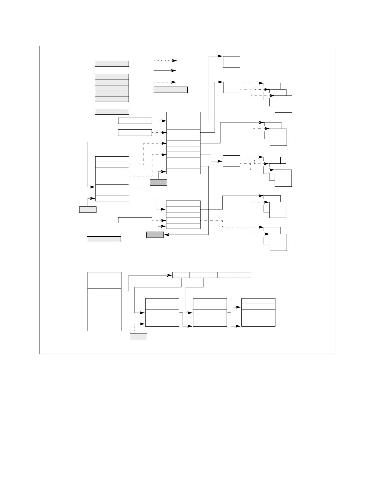
SYSTEM ARCHITECTURE OVERVIEW
EFLAGS Register
Physical Address
Code, Data or
Stack Segment
Linear Address
Control Registers
Task-State
CR4
Segment Selector
Segment (TSS)
Task
CR3
Code
CR2
Register
Data
CR1
CR0
Stack
Global Descriptor
Task Register
Table (GDT)
Interrupt Handler
Segment Sel.
Seg. Desc.
Code
Current
TSS Seg. Sel.
TSS Desc.
Stack
Interrupt
TSS
Vector
Seg. Desc.
Interrupt Descriptor
Task-State
Table (IDT)
Segment (TSS)
TSS Desc.
Task
Code
Interrupt Gate
LDT Desc.
Data
Stack
Task Gate
GDTR
Trap Gate
Local Descriptor
Exception Handler
Table (LDT)
Code
Current
Stack
Call-Gate
TSS
IDTR
Seg. Desc.
Segment Selector
Call Gate
Protected Procedure
Code
XCR0 (XFEM)
Current
LDTR
TSS
Stack
Linear Address Space
Linear Address
Dir
Table
Offset
Linear Addr.
Page Directory
Page Table
Page
Physical Addr.
Pg. Dir. Entry
Pg. Tbl. Entry
0
This page mapping example is for 4-KByte pages
CR3*
and 32-bit paging.
*Physical Address
Figure 2-1. IA-32 System-Level Registers and Data Structures
2-2
Vol. 3A
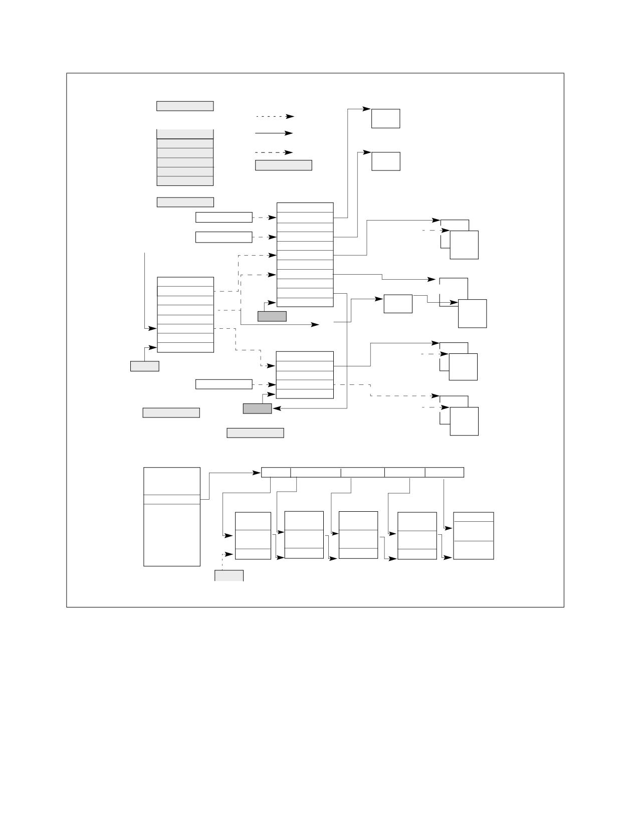
SYSTEM ARCHITECTURE OVERVIEW
RFLAGS
Physical Address
Code, Data or Stack
Control Register
Segment (Base =0)
Linear Address
CR8
Task-State
CR4
Segment Selector
Segment (TSS)
CR3
CR2
Register
CR1
CR0
Global Descriptor
Task Register
Table (GDT)
Interrupt Handler
Segment Sel.
Seg. Desc.
Code
NULL
Interrupt
TR
TSS Desc.
Stack
Vector
Seg. Desc.
Interrupt Descriptor
Table (IDT)
Interr. Handler
Seg. Desc.
Code
Interrupt Gate
LDT Desc.
Current TSS
Stack
Interrupt Gate
GDTR
IST
Trap Gate
Local Descriptor
Exception Handler
Table (LDT)
Code
NULL
Stack
IDTR
Call-Gate
Seg. Desc.
Segment Selector
Call Gate
Protected Procedure
XCR0 (XFEM)
Code
LDTR
NULL
Stack
PKRU
Linear Address Space
Linear Address
PML4
Dir. Pointer
Directory
T
able
Offset
Linear Addr.
PML4
Pg. Dir
. Ptr.
Page Dir.
Page Table
Page
Physical
PML4.
Pg. Dir.
Page Tbl
Addr.
Entry
Entry
Entry
0
This page mapping example is for 4-KByte pages
CR3*
and 4-level paging.
*Physical Address
Figure 2-2. System-Level Registers and Data Structures in IA-32e Mode and 4-Level Paging
2.1.1
Global and Local Descriptor Tables
When operating in protected mode, all memory accesses pass through either the global descriptor table (GDT) or
an optional local descriptor table (LDT) as shown in Figure 2-1. These tables contain entries called segment
descriptors. Segment descriptors provide the base address of segments well as access rights, type, and usage
information.
Vol. 3A
2-3
SYSTEM ARCHITECTURE OVERVIEW
Each segment descriptor has an associated segment selector. A segment selector provides the software that uses
it with an index into the GDT or LDT (the offset of its associated segment descriptor), a global/local flag (deter-
mines whether the selector points to the GDT or the LDT), and access rights information.
To access a byte in a segment, a segment selector and an offset must be supplied. The segment selector provides
access to the segment descriptor for the segment (in the GDT or LDT). From the segment descriptor, the processor
obtains the base address of the segment in the linear address space. The offset then provides the location of the
byte relative to the base address. This mechanism can be used to access any valid code, data, or stack segment,
provided the segment is accessible from the current privilege level (CPL) at which the processor is operating. The
CPL is defined as the protection level of the currently executing code segment.
See Figure 2-1. The solid arrows in the figure indicate a linear address, dashed lines indicate a segment selector,
and the dotted arrows indicate a physical address. For simplicity, many of the segment selectors are shown as
direct pointers to a segment. However, the actual path from a segment selector to its associated segment is always
through a GDT or LDT.
The linear address of the base of the GDT is contained in the GDT register (GDTR); the linear address of the LDT is
contained in the LDT register (LDTR).
2.1.1.1
Global and Local Descriptor Tables in IA-32e Mode
GDTR and LDTR registers are expanded to 64-bits wide in both IA-32e sub-modes (64-bit mode and compatibility
mode). For more information: see Section 3.5.2, “Segment Descriptor Tables in IA-32e Mode.”
Global and local descriptor tables are expanded in 64-bit mode to support 64-bit base addresses, (16-byte LDT
descriptors hold a 64-bit base address and various attributes). In compatibility mode, descriptors are not
expanded.
2.1.2
System Segments, Segment Descriptors, and Gates
Besides code, data, and stack segments that make up the execution environment of a program or procedure, the
architecture defines two system segments: the task-state segment (TSS) and the LDT. The GDT is not considered
a segment because it is not accessed by means of a segment selector and segment descriptor. TSSs and LDTs have
segment descriptors defined for them.
The architecture also defines a set of special descriptors called gates (call gates, interrupt gates, trap gates, and
task gates). These provide protected gateways to system procedures and handlers that may operate at a different
privilege level than application programs and most procedures. For example, a CALL to a call gate can provide
access to a procedure in a code segment that is at the same or a numerically lower privilege level (more privileged)
than the current code segment. To access a procedure through a call gate, the calling procedure1 supplies the
selector for the call gate. The processor then performs an access rights check on the call gate, comparing the CPL
with the privilege level of the call gate and the destination code segment pointed to by the call gate.
If access to the destination code segment is allowed, the processor gets the segment selector for the destination
code segment and an offset into that code segment from the call gate. If the call requires a change in privilege
level, the processor also switches to the stack for the targeted privilege level. The segment selector for the new
stack is obtained from the TSS for the currently running task. Gates also facilitate transitions between 16-bit and
32-bit code segments, and vice versa.
2.1.2.1
Gates in IA-32e Mode
In IA-32e mode, the following descriptors are 16-byte descriptors (expanded to allow a 64-bit base): LDT descrip-
tors, 64-bit TSSs, call gates, interrupt gates, and trap gates.
Call gates facilitate transitions between 64-bit mode and compatibility mode. Task gates are not supported in IA-
32e mode. On privilege level changes, stack segment selectors are not read from the TSS. Instead, they are set to
NULL.
1. The word “procedure” is commonly used in this document as a general term for a logical unit or block of code (such as a program, pro-
cedure, function, or routine).
2-4
Vol. 3A
SYSTEM ARCHITECTURE OVERVIEW
2.1.3
Task-State Segments and Task Gates
The TSS (see Figure 2-1) defines the state of the execution environment for a task. It includes the state of general-
purpose registers, segment registers, the EFLAGS register, the EIP register, and segment selectors with stack
pointers for three stack segments (one stack for each privilege level). The TSS also includes the segment selector
for the LDT associated with the task and the base address of the paging-structure hierarchy.
All program execution in protected mode happens within the context of a task (called the current task). The
segment selector for the TSS for the current task is stored in the task register. The simplest method for switching
to a task is to make a call or jump to the new task. Here, the segment selector for the TSS of the new task is given
in the CALL or JMP instruction. In switching tasks, the processor performs the following actions:
1. Stores the state of the current task in the current TSS.
2. Loads the task register with the segment selector for the new task.
3. Accesses the new TSS through a segment descriptor in the GDT.
4. Loads the state of the new task from the new TSS into the general-purpose registers, the segment registers,
the LDTR, control register CR3 (base address of the paging-structure hierarchy), the EFLAGS register, and the
EIP register.
5. Begins execution of the new task.
A task can also be accessed through a task gate. A task gate is similar to a call gate, except that it provides access
(through a segment selector) to a TSS rather than a code segment.
2.1.3.1
Task-State Segments in IA-32e Mode
Hardware task switches are not supported in IA-32e mode. However, TSSs continue to exist. The base address of
a TSS is specified by its descriptor.
A 64-bit TSS holds the following information that is important to 64-bit operation:
• Stack pointer addresses for each privilege level.
• Pointer addresses for the interrupt stack table.
• Offset address of the IO-permission bitmap (from the TSS base).
The task register is expanded to hold 64-bit base addresses in IA-32e mode. See also: Section 8.7, “Task Manage-
ment in 64-bit Mode.”
2.1.4
Interrupt and Exception Handling
External interrupts, software interrupts and exceptions are handled through the interrupt descriptor table (IDT).
The IDT stores a collection of gate descriptors that provide access to interrupt and exception handlers. Like the
GDT, the IDT is not a segment. The linear address for the base of the IDT is contained in the IDT register (IDTR).
Gate descriptors in the IDT can be interrupt, trap, or task gate descriptors. To access an interrupt or exception
handler, the processor first receives an interrupt vector from internal hardware, an external interrupt controller, or
from software by means of an INT n, INTO, INT3, INT1, or BOUND instruction. The interrupt vector provides an
index into the IDT. If the selected gate descriptor is an interrupt gate or a trap gate, the associated handler proce-
dure is accessed in a manner similar to calling a procedure through a call gate. If the descriptor is a task gate, the
handler is accessed through a task switch.
2.1.4.1
Interrupt and Exception Handling IA-32e Mode
In IA-32e mode, interrupt gate descriptors are expanded to 16 bytes to support 64-bit base addresses. This is true
for 64-bit mode and compatibility mode.
The IDTR register is expanded to hold a 64-bit base address. Task gates are not supported.
Vol. 3A
2-5
SYSTEM ARCHITECTURE OVERVIEW
2.1.5
Memory Management
System architecture supports either direct physical addressing of memory or virtual memory (through paging).
When physical addressing is used, a linear address is treated as a physical address. When paging is used: all code,
data, stack, and system segments (including the GDT and IDT) can be paged with only the most recently accessed
pages being held in physical memory.
The location of pages (sometimes called page frames) in physical memory is contained in the paging structures.
These structures reside in physical memory (see Figure 2-1 for the case of 32-bit paging).
The base physical address of the paging-structure hierarchy is contained in control register CR3. The entries in the
paging structures determine the physical address of the base of a page frame, access rights and memory manage-
ment information.
To use this paging mechanism, a linear address is broken into parts. The parts provide separate offsets into the
paging structures and the page frame. A system can have a single hierarchy of paging structures or several. For
example, each task can have its own hierarchy.
2.1.5.1
Memory Management in IA-32e Mode
In IA-32e mode, physical memory pages are managed by a set of system data structures. In both compatibility
mode and 64-bit mode, four or five levels of system data structures are used (see Chapter 4, “Paging”). These
include the following:
• The page map level 5 (PML5) - An entry in the PML5 table contains the physical address of the base of a
PML4 table, access rights, and memory management information. The base physical address of the PML5 table
is stored in CR3. The PML5 table is used only with 5-level paging.
• A page map level 4 (PML4) - An entry in a PML4 table contains the physical address of the base of a page
directory pointer table, access rights, and memory management information. With 4-level paging, there is only
one PML4 table and its base physical address is stored in CR3.
• A set of page directory pointer tables - An entry in a page directory pointer table contains the physical
address of the base of a page directory table, access rights, and memory management information.
• Sets of page directories - An entry in a page directory table contains the physical address of the base of a
page table, access rights, and memory management information.
• Sets of page tables - An entry in a page table contains the physical address of a page frame, access rights,
and memory management information.
2.1.6
System Registers
To assist in initializing the processor and controlling system operations, the system architecture provides system
flags in the EFLAGS register and several system registers:
• The system flags and IOPL field in the EFLAGS register control task and mode switching, interrupt handling,
instruction tracing, and access rights. See also: Section 2.3, “System Flags and Fields in the EFLAGS Register.”
• The control registers (CR0, CR2, CR3, and CR4) contain a variety of flags and data fields for controlling system-
level operations. Other flags in these registers are used to indicate support for specific processor capabilities
within the operating system or executive. See also: Chapter 2, “Control Registers,” and Section 2.6, “Extended
Control Registers (Including XCR0).”
• The debug registers (not shown in Figure 2-1) allow the setting of breakpoints for use in debugging programs
and systems software. See also: Chapter 18, “Debug, Branch Profile, TSC, and Intel® Resource Director
Technology (Intel® RDT) Features.”
• The GDTR, LDTR, and IDTR registers contain the linear addresses and sizes (limits) of their respective tables.
See also: Section 2.4, “Memory-Management Registers.”
• The task register contains the linear address and size of the TSS for the current task. See also: Section 2.4,
“Memory-Management Registers.”
• Model-specific registers (not shown in Figure 2-1).
2-6
Vol. 3A
SYSTEM ARCHITECTURE OVERVIEW
The model-specific registers (MSRs) are a group of registers available primarily to operating-system or executive
procedures (that is, code running at privilege level 0). These registers control items such as the debug extensions,
the performance-monitoring counters, the machine- check architecture, and the memory type ranges (MTRRs).
The number and function of these registers varies among different members of the Intel 64 and IA-32 processor
families. See also: Section 10.4, “Model-Specific Registers (MSRs),” and Chapter 2, “Model-Specific Registers
(MSRs),” in the Intel® 64 and IA-32 Architectures Software Developer’s Manual, Volume 4.
Most systems restrict access to system registers (other than the EFLAGS register) by application programs.
Systems can be designed, however, where all programs and procedures run at the most privileged level (privilege
level 0). In such a case, application programs would be allowed to modify the system registers.
2.1.6.1
System Registers in IA-32e Mode
In IA-32e mode, the four system-descriptor-table registers (GDTR, IDTR, LDTR, and TR) are expanded in hardware
to hold 64-bit base addresses. EFLAGS becomes the 64-bit RFLAGS register. CR0-CR4 are expanded to 64 bits.
CR8 becomes available. CR8 provides read-write access to the task priority register (TPR) so that the operating
system can control the priority classes of external interrupts.
In 64-bit mode, debug registers DR0-DR7 are 64 bits. In compatibility mode, address-matching in DR0-DR3 is
also done at 64-bit granularity.
On systems that support IA-32e mode, the extended feature enable register (IA32_EFER) is available. This model-
specific register controls activation of IA-32e mode and other IA-32e mode operations. In addition, there are
several model-specific registers that govern IA-32e mode instructions:
• IA32_KERNEL_GS_BASE - Used by SWAPGS instruction.
• IA32_LSTAR - Used by SYSCALL instruction.
• IA32_FMASK - Used by SYSCALL instruction.
• IA32_STAR - Used by SYSCALL and SYSRET instruction.
2.1.7
Other System Resources
Besides the system registers and data structures described in the previous sections, system architecture provides
the following additional resources:
• Operating system instructions (see also: Section 2.8, “System Instruction Summary”).
• Performance-monitoring counters (not shown in Figure 2-1).
• Internal caches and buffers (not shown in Figure 2-1).
Performance-monitoring counters are event counters that can be programmed to count processor events such as
the number of instructions decoded, the number of interrupts received, or the number of cache loads.
The processor provides several internal caches and buffers. The caches are used to store both data and instruc-
tions. The buffers are used to store things like decoded addresses to system and application segments and write
operations waiting to be performed. See also: Chapter 12, “Memory Cache Control.”
2.2
MODES OF OPERATION
The IA-32 architecture supports three operating modes and one quasi-operating mode:
• Protected mode - This is the native operating mode of the processor. It provides a rich set of architectural
features, flexibility, high performance and backward compatibility to existing software base.
• Real-address mode - This operating mode provides the programming environment of the Intel 8086
processor, with a few extensions (such as the ability to switch to protected or system management mode).
• System management mode (SMM) - SMM is a standard architectural feature in all IA-32 processors,
beginning with the Intel386 SL processor. This mode provides an operating system or executive with a
transparent mechanism for implementing power management and OEM differentiation features. SMM is
entered through activation of an external system interrupt pin (SMI#), which generates a system management
Vol. 3A
2-7
SYSTEM ARCHITECTURE OVERVIEW
interrupt (SMI). In SMM, the processor switches to a separate address space while saving the context of the
currently running program or task. SMM-specific code may then be executed transparently. Upon returning
from SMM, the processor is placed back into its state prior to the SMI.
• Virtual-8086 mode - In protected mode, the processor supports a quasi-operating mode known as virtual-
8086 mode. This mode allows the processor execute 8086 software in a protected, multitasking environment.
Intel 64 architecture supports all operating modes of IA-32 architecture and IA-32e modes:
• IA-32e mode - In IA-32e mode, the processor supports two sub-modes: compatibility mode and 64-bit
mode. 64-bit mode provides 64-bit linear addressing and support for physical address space larger than 64
GBytes. Compatibility mode allows most legacy protected-mode applications to run unchanged.
Figure 2-3 shows how the processor moves between operating modes.
SMI#
Real-Address
Mode
Reset
or
Reset or
RSM
PE=1
PE=0
SMI#
Reset
Protected Mode
RSM
System
Management
LME=1, CR0.PG=1*
SMI#
Mode
See**
IA-32e
RSM
Mode
VM=0
VM=1
* See Section 10.8.5
SMI#
** See Section 10.8.5.4
Virtual-8086
Mode
RSM
Figure 2-3. Transitions Among the Processor’s Operating Modes
The processor is placed in real-address mode following power-up or a reset. The PE flag in control register CR0 then
controls whether the processor is operating in real-address or protected mode. See also: Section 10.9, “Mode
Switching,” and Section 4.1.2, “Paging-Mode Enabling.”
The VM flag in the EFLAGS register determines whether the processor is operating in protected mode or virtual-
8086 mode. Transitions between protected mode and virtual-8086 mode are generally carried out as part of a task
switch or a return from an interrupt or exception handler. See also: Section 21.2.5, “Entering Virtual-8086 Mode.”
The LMA bit (IA32_EFER.LMA[bit 10]) determines whether the processor is operating in IA-32e mode. When
running in IA-32e mode, 64-bit or compatibility sub-mode operation is determined by CS.L bit of the code segment.
The processor enters into IA-32e mode from protected mode by enabling paging and setting the LME bit
(IA32_EFER.LME[bit 8]). See also: Chapter 10, “Processor Management and Initialization.”
The processor switches to SMM whenever it receives an SMI while the processor is in real-address, protected,
virtual-8086, or IA-32e modes. Upon execution of the RSM instruction, the processor always returns to the mode
it was in when the SMI occurred.
2-8
Vol. 3A
SYSTEM ARCHITECTURE OVERVIEW
2.2.1
Extended Feature Enable Register
The IA32_EFER MSR provides several fields related to IA-32e mode enabling and operation. It also provides one
field that relates to page-access right modification (see Section 4.6, “Access Rights”). The layout of the IA32_EFER
MSR is shown in Figure 2-4.
63
12 11 10 9
8
7
1
0
IA32_EFER
Execute Disable Bit Enable
IA-32e Mode Active
IA-32e Mode Enable
SYSCALL Enable
Reserved
Figure 2-4. IA32_EFER MSR Layout
Table 2-1. IA32_EFER MSR Information
Bit
Description
0
SYSCALL Enable: IA32_EFER.SCE (R/W)
Enables SYSCALL/SYSRET instructions in 64-bit mode.
7:1
Reserved.
8
IA-32e Mode Enable: IA32_EFER.LME (R/W)
Enables IA-32e mode operation.
9
Reserved.
10
IA-32e Mode Active: IA32_EFER.LMA (R)
Indicates IA-32e mode is active when set.
11
Execute Disable Bit Enable: IA32_EFER.NXE (R/W)
Enables page access restriction by preventing instruction fetches from PAE pages with the XD bit set (See Section 4.6).
63:12
Reserved.
2.3
SYSTEM FLAGS AND FIELDS IN THE EFLAGS REGISTER
The system flags and IOPL field of the EFLAGS register control I/O, maskable hardware interrupts, debugging, task
switching, and the virtual-8086 mode (see Figure 2-5). Only privileged code (typically operating system or execu-
tive code) should be allowed to modify these bits.
The system flags and IOPL are:
TF
Trap (bit 8) - Set to enable single-step mode for debugging; clear to disable single-step mode. In single-
step mode, the processor generates a debug exception after each instruction. This allows the execution
state of a program to be inspected after each instruction. If an application program sets the TF flag using a
Vol. 3A
2-9
SYSTEM ARCHITECTURE OVERVIEW
POPF, POPFD, or IRET instruction, a debug exception is generated after the instruction that follows the
POPF, POPFD, or IRET.
31
22 21 20 19 18 17 16
15 14 13 12 11 10 9
8
7
6
5
4
3
2
1
0
I
V
V
I
A
V
R
N
O
O
D
I
T
S
Z
A
P
C
Reserved (set to 0)
I
I
0
0
0
1
D
C
M
F
T
P
F
F
F
F
F
F
F
F
F
P
F
L
ID
- Identification Flag
VIP - Virtual Interrupt Pending
VIF - Virtual Interrupt Flag
AC - Alignment Check / Access Control
VM - Virtual-8086 Mode
RF - Resume Flag
NT - Nested Task Flag
IOPL- I/O Privilege Level
IF
- Interrupt Enable Flag
TF
- Trap Flag
Reserved
Figure 2-5. System Flags in the EFLAGS Register
IF
Interrupt enable (bit 9) - Controls the response of the processor to maskable hardware interrupt
requests (see also: Section 6.3.2, “Maskable Hardware Interrupts”). The flag is set to respond to maskable
hardware interrupts; cleared to inhibit maskable hardware interrupts. The IF flag does not affect the gener-
ation of exceptions or nonmaskable interrupts (NMI interrupts). The CPL, IOPL, and the state of the VME
flag in control register CR4 determine whether the IF flag can be modified by the CLI, STI, POPF, POPFD,
and IRET.
IOPL
I/O privilege level field (bits 12 and 13) - Indicates the I/O privilege level (IOPL) of the currently
running program or task. The CPL of the currently running program or task must be less than or equal to
the IOPL to access the I/O address space. The POPF and IRET instructions can modify this field only when
operating at a CPL of 0.
The IOPL is also one of the mechanisms that controls the modification of the IF flag and the handling of
interrupts in virtual-8086 mode when virtual mode extensions are in effect (when CR4.VME = 1). See also:
Chapter 19, “Input/Output,” in the Intel® 64 and IA-32 Architectures Software Developer’s Manual, Volume
1.
NT
Nested task (bit 14) - Controls the chaining of interrupted and called tasks. The processor sets this flag
on calls to a task initiated with a CALL instruction, an interrupt, or an exception. It examines and modifies
this flag on returns from a task initiated with the IRET instruction. The flag can be explicitly set or cleared
with the POPF/POPFD instructions; however, changing to the state of this flag can generate unexpected
exceptions in application programs.
See also: Section 8.4, “Task Linking.”
RF
Resume (bit 16) - Controls the processor’s response to instruction-breakpoint conditions. When set, this
flag temporarily disables debug exceptions (#DB) from being generated for instruction breakpoints
(although other exception conditions can cause an exception to be generated). When clear, instruction
breakpoints will generate debug exceptions.
The primary function of the RF flag is to allow the restarting of an instruction following a debug exception
that was caused by an instruction breakpoint condition. Here, debug software must set this flag in the
EFLAGS image on the stack just prior to returning to the interrupted program with IRETD (to prevent the
instruction breakpoint from causing another debug exception). The processor then automatically clears
this flag after the instruction returned to has been successfully executed, enabling instruction breakpoint
faults again.
See also: Section 18.3.1.1, “Instruction-Breakpoint Exception Condition.”
VM
Virtual-8086 mode (bit 17) - Set to enable virtual-8086 mode; clear to return to protected mode.
2-10
Vol. 3A
SYSTEM ARCHITECTURE OVERVIEW
See also: Section 21.2.1, “Enabling Virtual-8086 Mode.”
AC
Alignment check or access control (bit 18) - If the AM bit is set in the CR0 register, alignment
checking of user-mode data accesses is enabled if and only if this flag is 1. An alignment-check exception
is generated when reference is made to an unaligned operand, such as a word at an odd byte address or a
doubleword at an address which is not an integral multiple of four. Alignment-check exceptions are gener-
ated only in user mode (privilege level 3). Memory references that default to privilege level 0, such as
segment descriptor loads, do not generate this exception even when caused by instructions executed in
user-mode.
The alignment-check exception can be used to check alignment of data. This is useful when exchanging
data with processors which require all data to be aligned. The alignment-check exception can also be used
by interpreters to flag some pointers as special by misaligning the pointer. This eliminates overhead of
checking each pointer and only handles the special pointer when used.
If the SMAP bit is set in the CR4 register, explicit supervisor-mode data accesses to user-mode pages are
allowed if and only if this bit is 1. See Section 4.6, “Access Rights.”
VIF
Virtual Interrupt (bit 19) - Contains a virtual image of the IF flag. This flag is used in conjunction with
the VIP flag. The processor only recognizes the VIF flag when either the VME flag or the PVI flag in control
register CR4 is set and the IOPL is less than 3. (The VME flag enables the virtual-8086 mode extensions;
the PVI flag enables the protected-mode virtual interrupts.)
See also: Section 21.3.3.5, “Method 6: Software Interrupt Handling,” and Section 21.4, “Protected-Mode
Virtual Interrupts.”
VIP
Virtual interrupt pending (bit 20) - Set by software to indicate that an interrupt is pending; cleared to
indicate that no interrupt is pending. This flag is used in conjunction with the VIF flag. The processor reads
this flag but never modifies it. The processor only recognizes the VIP flag when either the VME flag or the
PVI flag in control register CR4 is set and the IOPL is less than 3. The VME flag enables the virtual-8086
mode extensions; the PVI flag enables the protected-mode virtual interrupts.
See Section 21.3.3.5, “Method 6: Software Interrupt Handling,” and Section 21.4, “Protected-Mode Virtual
Interrupts.”
ID
Identification (bit 21) - The ability of a program or procedure to set or clear this flag indicates support
for the CPUID instruction.
2.3.1
System Flags and Fields in IA-32e Mode
In 64-bit mode, the RFLAGS register expands to 64 bits with the upper 32 bits reserved. System flags in RFLAGS
(64-bit mode) or EFLAGS (compatibility mode) are shown in Figure 2-5.
In IA-32e mode, the processor does not allow the VM bit to be set because virtual-8086 mode is not supported
(attempts to set the bit are ignored). Also, the processor will not set the NT bit. The processor does, however, allow
software to set the NT bit (note that an IRET causes a general protection fault in IA-32e mode if the NT bit is set).
In IA-32e mode, the SYSCALL/SYSRET instructions have a programmable method of specifying which bits are
cleared in RFLAGS/EFLAGS. These instructions save/restore EFLAGS/RFLAGS.
2.4
MEMORY-MANAGEMENT REGISTERS
The processor provides four memory-management registers (GDTR, LDTR, IDTR, and TR) that specify the locations
of the data structures which control segmented memory management (see Figure 2-6). Special instructions are
provided for loading and storing these registers.
Vol. 3A
2-11
SYSTEM ARCHITECTURE OVERVIEW
System Table Registers
47(79)
16 15
0
GDTR
32(64)-bit Linear Base Address
16-Bit Table Limit
IDTR
32(64)-bit Linear Base Address
16-Bit Table Limit
System Segment
Segment Descriptor Registers (Automatically Loaded)
Registers
15
0
Attributes
Task
Seg. Sel.
32(64)-bit Linear Base Address
Segment Limit
Register
LDTR
Seg. Sel.
32(64)-bit Linear Base Address
Segment Limit
Figure 2-6. Memory Management Registers
2.4.1
Global Descriptor Table Register (GDTR)
The GDTR register holds the base address (32 bits in protected mode; 64 bits in IA-32e mode) and the 16-bit table
limit for the GDT. The base address specifies the linear address of byte 0 of the GDT; the table limit specifies the
number of bytes in the table.
The LGDT and SGDT instructions load and store the GDTR register, respectively. On power up or reset of the
processor, the base address is set to the default value of 0 and the limit is set to 0FFFFH. A new base address must
be loaded into the GDTR as part of the processor initialization process for protected-mode operation.
See also: Section 3.5.1, “Segment Descriptor Tables.”
2.4.2
Local Descriptor Table Register (LDTR)
The LDTR register holds the 16-bit segment selector, base address (32 bits in protected mode; 64 bits in IA-32e
mode), segment limit, and descriptor attributes for the LDT. The base address specifies the linear address of byte
0 of the LDT segment; the segment limit specifies the number of bytes in the segment. See also: Section 3.5.1,
“Segment Descriptor Tables.”
The LLDT and SLDT instructions load and store the segment selector part of the LDTR register, respectively. The
segment that contains the LDT must have a segment descriptor in the GDT. When the LLDT instruction loads a
segment selector in the LDTR: the base address, limit, and descriptor attributes from the LDT descriptor are auto-
matically loaded in the LDTR.
When a task switch occurs, the LDTR is automatically loaded with the segment selector and descriptor for the LDT
for the new task. The contents of the LDTR are not automatically saved prior to writing the new LDT information
into the register.
On power up or reset of the processor, the segment selector and base address are set to the default value of 0 and
the limit is set to 0FFFFH.
2.4.3
IDTR Interrupt Descriptor Table Register
The IDTR register holds the base address (32 bits in protected mode; 64 bits in IA-32e mode) and 16-bit table limit
for the IDT. The base address specifies the linear address of byte 0 of the IDT; the table limit specifies the number
of bytes in the table. The LIDT and SIDT instructions load and store the IDTR register, respectively. On power up or
reset of the processor, the base address is set to the default value of 0 and the limit is set to 0FFFFH. The base
address and limit in the register can then be changed as part of the processor initialization process.
See also: Section 6.10, “Interrupt Descriptor Table (IDT).”
2-12
Vol. 3A
SYSTEM ARCHITECTURE OVERVIEW
2.4.4
Task Register (TR)
The task register holds the 16-bit segment selector, base address (32 bits in protected mode; 64 bits in IA-32e
mode), segment limit, and descriptor attributes for the TSS of the current task. The selector references the TSS
descriptor in the GDT. The base address specifies the linear address of byte 0 of the TSS; the segment limit speci-
fies the number of bytes in the TSS. See also: Section 8.2.4, “Task Register.”
The LTR and STR instructions load and store the segment selector part of the task register, respectively. When the
LTR instruction loads a segment selector in the task register, the base address, limit, and descriptor attributes from
the TSS descriptor are automatically loaded into the task register. On power up or reset of the processor, the base
address is set to the default value of 0 and the limit is set to 0FFFFH.
When a task switch occurs, the task register is automatically loaded with the segment selector and descriptor for
the TSS for the new task. The contents of the task register are not automatically saved prior to writing the new TSS
information into the register.
2.5
CONTROL REGISTERS
Control registers (CR0, CR1, CR2, CR3, and CR4; see Figure 2-7) determine operating mode of the processor and
the characteristics of the currently executing task. These registers are 32 bits in all 32-bit modes and compatibility
mode.
In 64-bit mode, control registers are expanded to 64 bits. The MOV CRn instructions are used to manipulate the
register bits. Operand-size prefixes for these instructions are ignored. The following is also true:
• The control registers can be read and loaded (or modified) using the move-to-or-from-control-registers forms
of the MOV instruction. In protected mode, the MOV instructions allow the control registers to be read or loaded
(at privilege level 0 only). This restriction means that application programs or operating-system procedures
(running at privilege levels 1, 2, or 3) are prevented from reading or loading the control registers.
• Some of the bits in CR0 and CR4 are reserved and must be written with zeros. Attempting to set any reserved
bits in CR0[31:0] is ignored. Attempting to set any reserved bits in CR0[63:32] results in a general-protection
exception, #GP(0). Attempting to set any reserved bits in CR4 results in a general-protection exception,
#GP(0).
• All 64 bits of CR2 are writable by software.
• Reserved bits in CR3[63:MAXPHYADDR] must be zero. Attempting to set any of them results in #GP(0).
• The MOV CR2 instruction does not check that address written to CR2 is canonical.
• A 64-bit capable processor will retain the upper 32 bits of each control register when transitioning out of IA-32e
mode.
• On a 64-bit capable processor, an execution of MOV to CR outside of 64-bit mode zeros the upper 32 bits of the
control register.
• Register CR8 is available in 64-bit mode only.
The control registers are summarized below, and each architecturally defined control field in these control registers
is described individually. In Figure 2-7, the width of the register in 64-bit mode is indicated in parenthesis (except
for CR0).
• CR0 - Contains system control flags that control operating mode and states of the processor.
• CR1 - Reserved.
• CR2 - Contains the page-fault linear address (the linear address that caused a page fault).
• CR3 - Contains the physical address of the base of the paging-structure hierarchy and two flags (PCD and
PWT). Only the most-significant bits (less the lower 12 bits) of the base address are specified; the lower 12 bits
of the address are assumed to be 0. The first paging structure must thus be aligned to a page (4-KByte)
boundary. The PCD and PWT flags control caching of that paging structure in the processor’s internal data
caches (they do not control TLB caching of page-directory information).
When using the physical address extension, the CR3 register contains the base address of the page-directory-
pointer table. With 4-level paging and 5-level paging, the CR3 register contains the base address of the PML4
Vol. 3A
2-13
SYSTEM ARCHITECTURE OVERVIEW
table and PML5 table, respectively. If PCIDs are enabled, CR3 has a format different from that illustrated in
Figure 2-7. See Section 4.5, “4-Level Paging and 5-Level Paging.”
See also: Chapter 4, “Paging.”
• CR4 - Contains a group of flags that enable several architectural extensions, and indicate operating system or
executive support for specific processor capabilities. Bits CR4[63:32] can only be used for IA-32e mode only
features that are enabled after entering 64-bit mode. Bits CR4[63:32] do not have any effect outside of IA-32e
mode.
• CR8 - Provides read and write access to the Task Priority Register (TPR). It specifies the priority threshold
value that operating systems use to control the priority class of external interrupts allowed to interrupt the
processor. This register is available only in 64-bit mode. However, interrupt filtering continues to apply in
compatibility mode.
31 (63)
25
24
23
22
21
20
19
18
17
16
15
14
13
12
11
10
9
8
7
6
5
4
3
2
1
0
U
P
S
S
S
V
L
U
I
P
C
P
C
P
P
M
P
P
T
P
V
M
M
K
M
M
A
M
D
Reserved
N
K
E
K
I
C
G
C
A
S
S
V
M
CR4
A
E
L
X
X
5
I
E
T
S
T
E
D
E
E
E
E
E
D
I
E
P
P
E
E
7
P
R
E
OSFXSR
OSXSAVE
FSGSBASE
OSXMMEXCPT
31 (63)
12
11
5
4
3
2
0
P
P
Page-Directory Base
C
W
CR3
D
T
31 (63)
0
Page-Fault Linear Address
CR2
31 (63)
0
CR1
31
30
29
28
19
18
17
16
15
6
5
4
3
2
1
0
P
C
N
A
W
N
E
T
E
M
P
G
D
W
M
P
E
T
S
M
P
E
CR0
Reserved
Figure 2-7. Control Registers
2-14
Vol. 3A
SYSTEM ARCHITECTURE OVERVIEW
The flags in control registers are:
CR0.PG
Paging (bit 31 of CR0) - Enables paging when set; disables paging when clear. When paging is
disabled, all linear addresses are treated as physical addresses. The PG flag has no effect if the PE flag (bit
0 of register CR0) is not also set; setting the PG flag when the PE flag is clear causes a general-protection
exception (#GP). See also: Chapter 4, “Paging.”
On Intel 64 processors, enabling and disabling IA-32e mode operation also requires modifying CR0.PG.
CR0.CD
Cache Disable (bit 30 of CR0) - When the CD and NW flags are clear, caching of memory locations for
the whole of physical memory in the processor’s internal (and external) caches is enabled. When the CD
flag is set, caching is restricted as described in Table 12-5. To prevent the processor from accessing and
updating its caches, the CD flag must be set and the caches must be invalidated so that no cache hits can
occur.
See also: Section 12.5.3, “Preventing Caching,” and Section 12.5, “Cache Control.”
CR0.NW
Not Write-through (bit 29 of CR0) - When the NW and CD flags are clear, write-back (for Pentium 4,
Intel Xeon, P6 family, and Pentium processors) or write-through (for Intel486 processors) is enabled for
writes that hit the cache and invalidation cycles are enabled. See Table 12-5 for detailed information about
the effect of the NW flag on caching for other settings of the CD and NW flags.
CR0.AM
Alignment Mask (bit 18 of CR0) - Enables automatic alignment checking when set; disables alignment
checking when clear. Alignment checking is performed only when the AM flag is set, the AC flag in the
EFLAGS register is set, CPL is 3, and the processor is operating in either protected or virtual-8086 mode.
CR0.WP
Write Protect (bit 16 of CR0) - When set, inhibits supervisor-level procedures from writing into read-
only pages; when clear, allows supervisor-level procedures to write into read-only pages (regardless of the
U/S bit setting; see Section 4.1.3 and Section 4.6). This flag facilitates implementation of the copy-on-
write method of creating a new process (forking) used by operating systems such as UNIX. This flag must
be set before software can set CR4.CET, and it cannot be cleared as long as CR4.CET = 1 (see below).
CR0.NE
Numeric Error (bit 5 of CR0) - Enables the native (internal) mechanism for reporting x87 FPU errors
when set; enables the PC-style x87 FPU error reporting mechanism when clear. When the NE flag is clear
and the IGNNE# input is asserted, x87 FPU errors are ignored. When the NE flag is clear and the IGNNE#
input is deasserted, an unmasked x87 FPU error causes the processor to assert the FERR# pin to generate
an external interrupt and to stop instruction execution immediately before executing the next waiting
floating-point instruction or WAIT/FWAIT instruction.
The FERR# pin is intended to drive an input to an external interrupt controller (the FERR# pin emulates the
ERROR# pin of the Intel 287 and Intel 387 DX math coprocessors). The NE flag, IGNNE# pin, and FERR#
pin are used with external logic to implement PC-style error reporting. Using FERR# and IGNNE# to handle
floating-point exceptions is deprecated by modern operating systems; this non-native approach also limits
newer processors to operate with one logical processor active.
See also: Section 8.7, “Handling x87 FPU Exceptions in Software,” in Chapter 8, “Programming with the
x87 FPU,” and Appendix A, “EFLAGS Cross-Reference,” in the Intel® 64 and IA-32 Architectures Software
Developer’s Manual, Volume 1.
CR0.ET
Extension Type (bit 4 of CR0) - Reserved in the Pentium 4, Intel Xeon, P6 family, and Pentium proces-
sors. In the Pentium 4, Intel Xeon, and P6 family processors, this flag is hardcoded to 1. In the Intel386
and Intel486 processors, this flag indicates support of Intel 387 DX math coprocessor instructions when
set.
CR0.TS
Task Switched (bit 3 of CR0) - Allows the saving of the x87 FPU/MMX/SSE/SSE2/SSE3/SSSE3/SSE4
context on a task switch to be delayed until an x87 FPU/MMX/SSE/SSE2/SSE3/SSSE3/SSE4 instruction is
Vol. 3A
2-15
SYSTEM ARCHITECTURE OVERVIEW
actually executed by the new task. The processor sets this flag on every task switch and tests it when
executing x87 FPU/MMX/SSE/SSE2/SSE3/SSSE3/SSE4 instructions.
• If the TS flag is set and the EM flag (bit 2 of CR0) is clear, a device-not-available exception (#NM) is
raised prior to the execution of any x87 FPU/MMX/SSE/SSE2/SSE3/SSSE3/SSE4 instruction; with the
exception of PAUSE, PREFETCHh, SFENCE, LFENCE, MFENCE, MOVNTI, CLFLUSH, CRC32, and POPCNT.
See the paragraph below for the special case of the WAIT/FWAIT instructions.
• If the TS flag is set and the MP flag (bit 1 of CR0) and EM flag are clear, an #NM exception is not raised
prior to the execution of an x87 FPU WAIT/FWAIT instruction.
• If the EM flag is set, the setting of the TS flag has no effect on the execution of x87
FPU/MMX/SSE/SSE2/SSE3/SSSE3/SSE4 instructions.
Table 2-2 shows the actions taken when the processor encounters an x87 FPU instruction based on the
settings of the TS, EM, and MP flags. Table 13-1 and 14-1 show the actions taken when the processor
encounters an MMX/SSE/SSE2/SSE3/SSSE3/SSE4 instruction.
The processor does not automatically save the context of the x87 FPU, XMM, and MXCSR registers on a
task switch. Instead, it sets the TS flag, which causes the processor to raise an #NM exception whenever it
encounters an x87 FPU/MMX/SSE/SSE2/SSE3/SSSE3/SSE4 instruction in the instruction stream for the
new task (with the exception of the instructions listed above).
The fault handler for the #NM exception can then be used to clear the TS flag (with the CLTS instruction)
and save the context of the x87 FPU, XMM, and MXCSR registers. If the task never encounters an x87
FPU/MMX/SSE/SSE2/SSE3/SSSE3/SSE4 instruction, the x87 FPU/MMX/SSE/SSE2/SSE3/SSSE3/SSE4
context is never saved.
Table 2-2. Action Taken By x87 FPU Instructions for Different Combinations of EM, MP, and TS
CR0 Flags
x87 FPU Instruction Type
EM
MP
TS
Floating-Point
WAIT/FWAIT
0
0
0
Execute
Execute.
0
0
1
#NM Exception
Execute.
0
1
0
Execute
Execute.
0
1
1
#NM Exception
#NM exception.
1
0
0
#NM Exception
Execute.
1
0
1
#NM Exception
Execute.
1
1
0
#NM Exception
Execute.
1
1
1
#NM Exception
#NM exception.
CR0.EM
Emulation (bit 2 of CR0) - Indicates that the processor does not have an internal or external x87 FPU when set;
indicates an x87 FPU is present when clear. This flag also affects the execution of
MMX/SSE/SSE2/SSE3/SSSE3/SSE4 instructions.
When the EM flag is set, execution of an x87 FPU instruction generates a device-not-available exception
(#NM). This flag must be set when the processor does not have an internal x87 FPU or is not connected to
an external math coprocessor. Setting this flag forces all floating-point instructions to be handled by soft-
ware emulation. Table 10-3 shows the recommended setting of this flag, depending on the IA-32 processor
and x87 FPU or math coprocessor present in the system. Table 2-2 shows the interaction of the EM, MP, and
TS flags.
Also, when the EM flag is set, execution of an MMX instruction causes an invalid-opcode exception (#UD)
to be generated (see Table 13-1). Thus, if an IA-32 or Intel 64 processor incorporates MMX technology, the
EM flag must be set to 0 to enable execution of MMX instructions.
Similarly for SSE/SSE2/SSE3/SSSE3/SSE4 extensions, when the EM flag is set, execution of most
SSE/SSE2/SSE3/SSSE3/SSE4 instructions causes an invalid opcode exception (#UD) to be generated (see
2-16
Vol. 3A