PCI/PCI-X Family of Gigabit Ethernet Controllers. Software Developer’s Manual (2009) - page 2
Receive and Transmit Description
3.5.9.3
TCP/IP/UDP Header for the Last Frame
The controller makes the following changes to the headers for the last frame of a TCP
segmentation context:
Note: Last frame payload bytes = PAYLEN - (N * MSS)
• IPv4 Header
- IP Total Length = (last frame payload bytes + HDRLEN) - IPCSS
- IP Identification: incremented from last value (wrap around)
- IP Checksum
• IPv6 Header
• Payload Length = MSS + HDRLEN - IPCSS
• TCP Header
- Sequence Number update: Add previous TCP payload size to the previous sequence
number value. This is equivalent to adding the MSS to the previous sequence number.
- If FIN flag = 1b, set it in this last frame
- If PSH flag =1b, set it in this last frame
- TCP Checksum
• UDP Header
- UDP length: (last frame payload bytes + HDRLEN) - TUCSS
- UDP Checksum
3.6
IP/TCP/UDP Transmit Checksum Offloading
The previous section on TCP Segmentation offload describes the IP/TCP/UDP checksum
offloading mechanism used in conjunction with TCP Segmentation. The same underlying
mechanism can also be applied as a standalone feature. The main difference in normal packet mode
(non-TCP Segmentation) is that only the checksum fields in the IP/TCP/UDP headers need to be
updated.
Before taking advantage of the Ethernet controller’s enhanced checksum offload capability, a
checksum context must be initialized. For the normal transmit checksum offload feature, this task
is performed by providing the Ethernet controller with a TCP/IP Context Descriptor with TSE = 0b
to denote a non-segmentation context. For additional details on contexts, refer to Section 3.3.5.
Enabling the checksum offloading capability without first initializing the appropriate checksum
context leads to unpredictable results. Once the checksum context has been set, that context, is used
for all normal packet transmissions until a new context is loaded. Also, since checksum insertion is
controlled on a per packet basis, there is no need to clear/reset the context.
The Ethernet controller is capable of performing two transmit checksum calculations. Typically,
these would be used for TCP/IP and UDP/IP packet types, however, the mechanism is general
enough to support other checksums as well. Each checksum operates independently and provides
identical functionality. Only the IP checksum case is discussed as follows.
68
Receive and Transmit Description
Three fields in the TCP/IP Context Descriptor set the context of the IP checksum offloading
feature:
• IPCSS
This field specifies the byte offset form the start of the transferred data to the first byte to be
included in the checksum. Setting this value to 0b means that the first byte of the data is
included in the checksum. The maximum value for this field is 255. This is adequate for
typical applications.
Note: The IPCSS value needs to be less than the total DMA length to a packet. If this is not the case, the
result will be unpredictable.
• IPCSO
This field specifies where the resulting checksum should be placed. Again, this is limited to
the first 256 bytes of the packet and must be less than or equal to the total length of a given
packet. If this is not the case, the checksum is not inserted.
• IPCSE
This field specifies where the checksum should stop. A 16-bit value supports checksum
offloading of packets as large as 64KB. Setting the IPCSE field to all zeros means End-of-
Packet. In this way, the length of the packet does not need to be calculated.
As mentioned above, it is not necessary to set a new context for each new packet. In many cases,
the same checksum context can be used for a majority of the packet stream. In this case, some of
the offload feature only for a particular traffic type, thereby avoiding all context descriptors except
for the initial one.
69
Receive and Transmit Description
Note: This page intentionally left blank.
70

PCI Local Bus Interface
4
The PCI/PCI-X Family of Gigabit Ethernet Controllers are PCI 2.2 or 2.3 compliant devices and
implement the PCI-X Addendum to the PCI Local Bus Specification, Revision 1.0.
Note: The 82540EP/EM, 82541xx, and 82547GI/EI do not support PCI-X mode.
4.1
PCI Configuration
The PCI Specification requires implementation of PCI Configuration registers. After a system
reset, these registers are initially configured by the BIOS, and/or a “Plug and Play” aware
Operating System (OS). Device drivers read these registers to determine what resources (interrupt
number, memory mapping location, etc.) the BIOS and/or OS assigned to the Ethernet controller.
The 82547GI/EI uses a dedicated CSA port for its system bus connection. Logically, it still follows
PCI configuration. However, some configuration parameters, such as cache line, are irrelevant.
Additionally, the 82547GI/EI requires special interrupt configuration in the BIOS (see Section
4.5).
Note: The 82547GI/EI does not support 64-bit addressing.
Four different regions of the PCI configuration space are used.
Address
Item
Description
00h-3Ch
PCI
Section 2.3.1
DCh-E0h
PCI Power Management
Section 6.3.3
E4h-E8h
PCI-X
Section 4.1.1
F0h-FCh
Message Signaled Interrupta
Section 4.1.3.1
a.
Not applicable to the 82541xx and 82547GI/EI.
These spaces are linked into a linked list using the Capabilities Pointer field (Cap_Ptr) in the PCI
Configuration section.
The implementation of the PCI registers for the PCI/PCI-X Family of Gigabit Ethernet Controllers
are listed in Table 4-1:
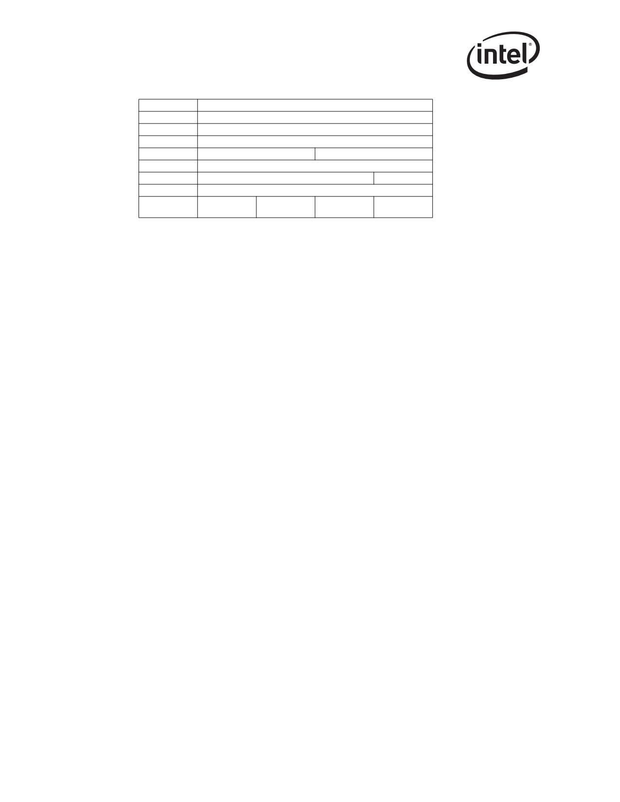
Table 4-1. Mandatory PCI Registers
Byte Offset
Byte 3
Byte 2
Byte 1
Byte 0
0h
Device ID
Vendor ID
4h
Status Register
Command Register
8h
Class Code (020000h)
Revision ID
Header Type
Latency
Cache Line
Ch
BIST (00h)
(00h)
Timer
Size
10h
Base Address 0a
4h
Base Address 1
18h
Base Address 2
71
PCI Local Bus Interface
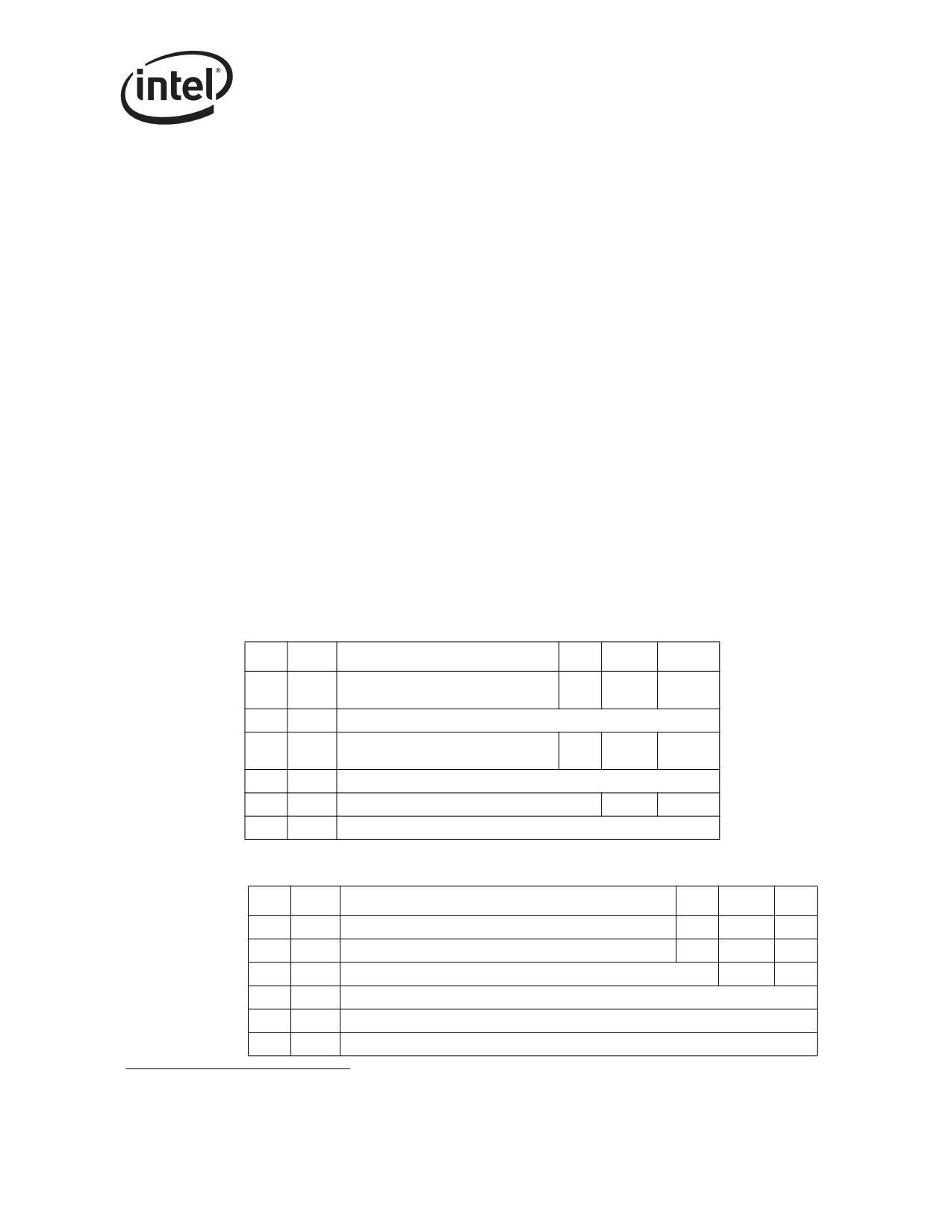
1Ch
Base Address 3 (unused)
20h
Base Address 4 (unused)
2h4
Base Address 5 (unused)
28h
Cardbus CIS Pointer (not used)
2Ch
Subsystem ID
Subsystem Vendor ID
30h
Expansion ROM Base Address
34h
Reserved
Cap_Ptr
38h
Reserved
Max_Latency
Min_Grant
Interrupt Pin
3Ch
Interrupt Line
(00h)
(FFh)
(01h)
a.
Refer to Table 4-2.
The following list provides explanations of the various PCI registers and their bit fields:
Vendor ID
This uniquely identifies all Intel PCI products. This field may be auto-loaded
from the EEPROM at power on or upon the assertion of PCI_RST#. A value of
8086h is the default for this field upon power up if the EEPROM does not
respond or is not programmed.
Device ID
This uniquely identifies the Ethernet controller. This field may be autoloaded
from the EEPROM at power on or upon the assertion of RST#. The default value
for this field is used upon power up if the EEPROM does not respond or is not
programmed.
Command Reg. The layout is listed in Table 4-3. Shaded bits are not used by this implementation
and are hard wired to 0b.
Status Register The layout is listed in Table 4-4. Shaded bits are not used by this implementation
and are hard wired to 0b.
Revision
Sequential stepping number starting with 00h for the A0 revision of the Ethernet
controller. Refer to the PCI/PCI-X Family of Gigabit Ethernet Controllers
Specification Update for the latest stepping information.
Class Code
The class code, 020000h identifies the Ethernet controller as an Ethernet adapter.
72
PCI Local Bus Interface
Cache Line Size1 Used to store the cache line size. The value is in units of 4 bytes. A system with a
cache line size of 64 bytes sets the value of this register to 10h. The only sizes
that are supported are 16, 32, 64, and 128 bytes. All other sizes are treated as 0b.
See the information about exceptions in Section 4.4.
Unsupported values affect PCI cache line support. All writes default to using the
memory write (MW) command, and memory read command determination uses
a cache line size of 32 bytes.
Latency Timer The lower two bits are not implemented and return 0b. The upper six bits are
Read/Write.
Header Type
This is for a normal single function Ethernet controller and reads 00h.
BIST
Built in Self-test is not implemented as supportable from PCI configuration
space in this version of the Ethernet controller.
Base Address Registers
The Base Address Registers (or BARs) are used to map the Ethernet con-
troller’s register space and flash to system memory space. In PCI-X mode
or in PCI mode when the BAR32 bit of the EEPROM is 0b, two registers
are used for each of the register space and the flash memory in order to
map 64-bit addresses. In PCI mode, if the BAR32 bit in the EEPROM is
1b, one register is used for each to map 32-bit addresses.
64-bit BARs
PCI-X mode with BAR32 bit in the EEPROM set to 0b.
Table 4-2. Base Address Registers
BAR
Addr.
31 4
3
2
1
0
Memory Register Base Address (bits
pref.
type
mem
0
10h
31:4)
1
14h
Memory Register Base Address (bits 63:32)
Memory Flash Base Address (bits
pref.
type
mem
2
18h
31:4)
3
1Ch
Memory Flash Base Address (bits 63:32)
4
20h
IO Register Base Address (bits 31:2)
0b
mem
5
24h
Reserved (read as all 0b’s)
32-bit BARs
Conventional PCI mode with BAR32 bit in the EEPROM set to 1b
BAR
Addr.
31
4
3
2
1
0
0
10h
Memory Register Base Address
pref.
type
mem
1
14h
Memory Flash Base Address
pref.
type
mem
2
18h
IO Register Base Address (bits 31:2)
0b
mem
3
1Ch
Reserved (read as all 0b’s)
4
20h
Reserved (read as all 0b’s)
5
24h
Reserved (read as all 0b’s)
1.
Not applicable to the 82547GI/EI.
73
PCI Local Bus Interface
All base address registers have the following fields:
Read/
Initial
Field
Bit(s)
Description
Write
Value
0b for
0b indicates memory space. 1b indicates I/O.
Mem
0
R
mem
1b for I/O
00b for 32-
Indicates the address space size.
bit
Type
2:1
R
00b = 32-bit
10b for 64-
10b = 64-bit
bit
0b = non-prefetchable space
1b = prefetchable space
Prefetch
3
R
0b
Ethernet controller implements non-prefetchable space
since it has read side-effects.
The lower bits of the address are hard-wired to 0b. The
upper bits can be written by the system software to set
the base address of the register or flash address space.
The memory register space is 128K bytes. The
Memory Register BAR has:
• Bits 16:4 are hard-wired to 0b.
• Bits 63:17 or 31:17 are read/write.
The size of the flash space can very between 64 KB and
512 KB depending on the FLASH size read from the
EEPROM. The Memory Flash BAR has these
characteristics:
Address
31:0
R/W
0b
Flash Size Valid Bits Zero Bits
(R/W) (RO)
•
64 KB 63/31:16 15:4
•
128 KB 63/31:17 16:4
•
256 KB 63/31:18 17:4
•
512 KB 63/31:19 18:4
The size of the IO register space is 8 bytes. The I/O
Register BAR has:
• Bit 2 hard-wired to 0b
• Bits 31:3 as read/write
74

PCI Local Bus Interface
Expansion ROM Base Address
This register is used to define the address and size information for boot-
time access to the optional Flash memory.
31
11
10
1
0
Expansion Rom Base Address
Reserved
En
Read/
Initial
Field
Bit(s)
Description
Write
Value
1b = Enables expansion ROM access.
En
0
R/W
0b
0b = Disables expansion ROM access.
Reserved
10:1
R
0b
Always read as 0b. Writes are ignored.
The lower bits of the address are hard-wired to 0b.
The upper bits can be written by the system software
to set the base address of the register or flash
address space.
Since the flash is used as the expansion ROM, the
size of the expansion ROM can very between 64 KB
and 512 KB, depending on the FLASH size read
Address
31:11
R/W
0b
from the EEPROM.
Flash Size Valid Bits Zero Bits:
•
64 KB 63/31:16 15:11
•
128 KB 63/31:17 16:11
•
256 KB 63/31:18 17:11
•
512 KB 63/31:19 18:11
CardBus CIS Pointer (82541PI/GI/EI and 82540EP Only)
When the Enable CLK_RUN# bit of the EEPROM’s Initialization Control
Word 2 and the 64/32 BAR bit of the EEPROM Initialization Control
Word 1 (indicating a 32-bit BAR) are both set to 1b, the Cardbus CIS
Pointer contains a value of 00000022h. Otherwise, it contains a value of
00000000h.
31
3
2
0
Offset
Space
75
PCI Local Bus Interface
Read/
Initial
Field
Bit(s)
Description
Write
Value
Indicates the address space where the CIS is
located.
0 = Configuration Space
1 = BAR0
2 = BAR1
Space
2:0
R/W
0 or 2
3 = BAR2
4 = BAR3
5 = BAR4
6 = BAR5
7 = Expansion ROM
Offset within the specified address space,
multiplied by eight. When enabled, the value
Offset
31:3
R
0 or 4
indicates that the CIS (Card Information
Structure) is at an offset of 4*8, or 32 bytes into
the Flash memory.
Subsystem ID
This value can be loaded automatically from the EEPROM upon power-up or
PCI reset. A value of 1008h is the default for this field upon power-up if the
EEPROM does not respond or is not programmed.
Subsystem Vendor ID
This value can be loaded automatically from the EEPROM upon power-up or
PCI reset. A value of 8086h is the default for this field upon power-up if the
EEPROM does not respond or is not programmed.
Cap_Ptr
The Capabilities Pointer field (Cap_Ptr) is an 8-bit field that provides an offset in
the Ethernet controller’s PCI Configuration Space for the location of the first
item in the Capabilities Linked List. The Ethernet controller sets this bit and then
implements a capabilities list to indicate that it supports PCI Power
Management, PCI-X, and Message Signaled Interrupts1. Its value is DCh which
is the address of the first entry: ACPI2 Power Management.
Address
Item
Next Pointer
DCh-E0h
ACPI Power Management
E4h
E4h-E8h
PCI-X
F0h
F0h-FCh
Message Signaled Interrupt
00h
Figure 4-1. Capabilities Linked List
In conventional PCI mode, Message Signaled interrupts can be disabled in the
EEPROM. If disabled, the message signaled interrupts won’t appear on the
linked list and PCI-X’s “Next Pointer” is 0b.
1.
Not applicable to the 82541xx or 82547GI/EI.
2.
Not applicable to the 82541ER.
76
PCI Local Bus Interface
Max_Lat/Min_Gnt1
The Ethernet controller places a very high load on the PCI bus during peak
transmit and receive traffic. In full duplex mode, it has a peak throughput
demand of 250 MB/sec. The peak delivered bandwidth on a 64-bit PCI bus at 33
MHz is 264 MB/sec, so the bus is fully saturated when transmit and receive are
operating simultaneously. In half duplex operation, the Ethernet controller has a
peak throughput demand of 125 MB/sec, which still puts an enormous load on
the PCI bus. Consequently, the Max_Lat should be small and is set to 00h, and
Min_Gnt is set to FFh indicating that the Ethernet controller requires a very high
priority and time slice.
Interrupt Pin
Read only register indicating which interrupt line (INTA# vs. INTB#) the
82546GB/EB uses. A value of 1b indicates that the 82546GB/EB uses INTA#
(as with all single-port Ethernet controllers). A value of 10b indicates that the
82546GB/EB uses INTB#.
For each separate device/function within the Ethernet controller, the value
reported here is based on the EEPROM Initialization Control Word 3 associated
with this controller, as well as whether both device/functions are enabled.
Provided both functions are enabled, then the value reported for each specific
function is based on the Interrupt Pin field of each Ethernet controller’s
Initialization Control Word 3.
If only a single internal device/function is enabled, then the value reported here
is 1b regardless of EEPROM configuration.
Interrupt Line
Read write register programmed by software to indicate which of the system
interrupt request lines this Ethernet controller’s interrupt pin is bound to. See the
PCI definition for more details.
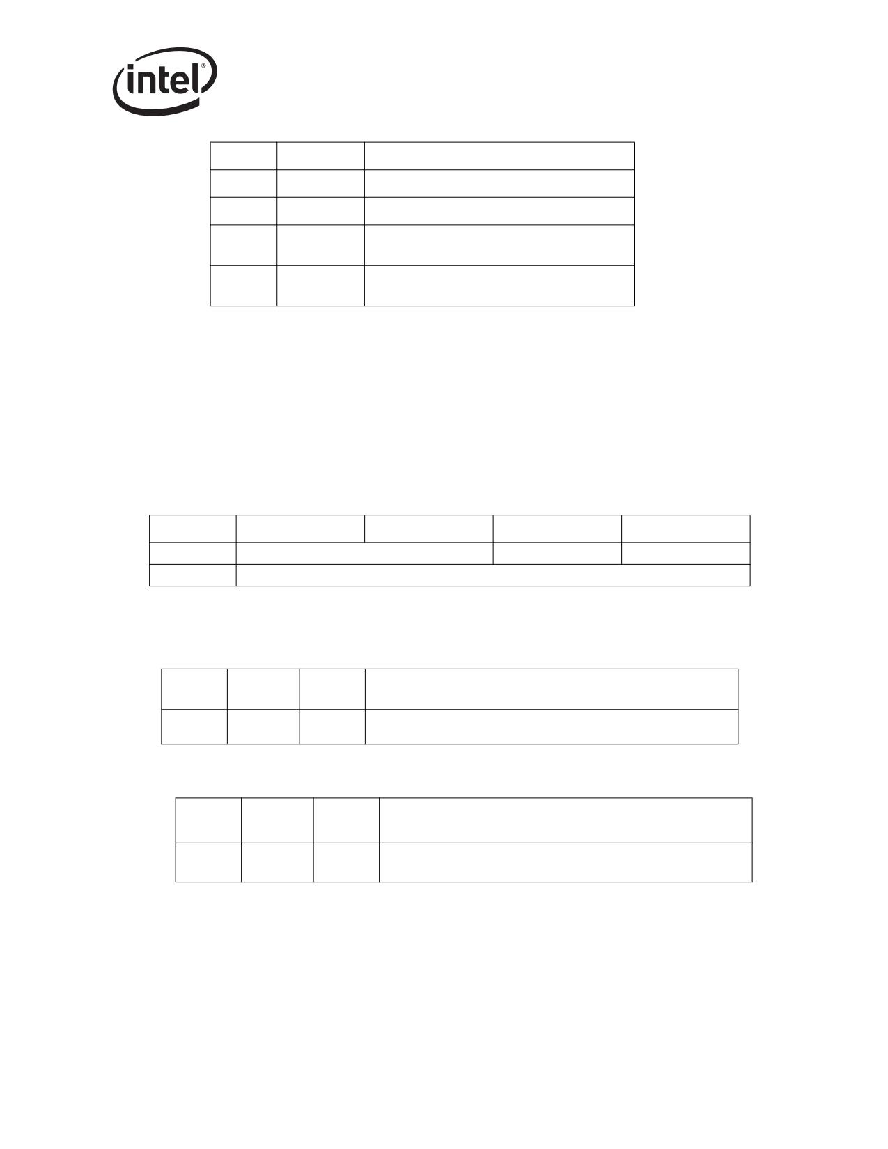
Table 4-3. Command Register Layout
15
10 9
0
Reserved
Command Bits
Bit(s)
Initial Value
Description
0
0b
I/O Access Enable.
1
0b
Memory Access Enable.
Enable Mastering. Ethernet controller in PCI-X
2
0b
mode is permitted to initiate a split completion
transaction regardless of the state of this bit.
3
0b
Special Cycle Monitoring.
1.
This bit is a don’t care for the 82547GI/EI.
77

PCI Local Bus Interface
Bit(s)
Initial Value
Description
Memory Write and Invalidate Enable (not
4
0b
applicable to the 82547GI/EI).
5
0b
Palette Snoop Enable.
Parity Error Response (not applicable to the
6
0b
82547GI/EI).
7
0b
Wait Cycle Enable.
8
0b
SERR# Enable (not applicable to the 82547GI/EI).
9
0b
Fast Back-to-Back Enable.
10a
0b
Interrupt Disable (INTA# or CSA signaled).
15:10
0b
Reserved.
15:11a
a.
82541xx and 82547GI/EI only.
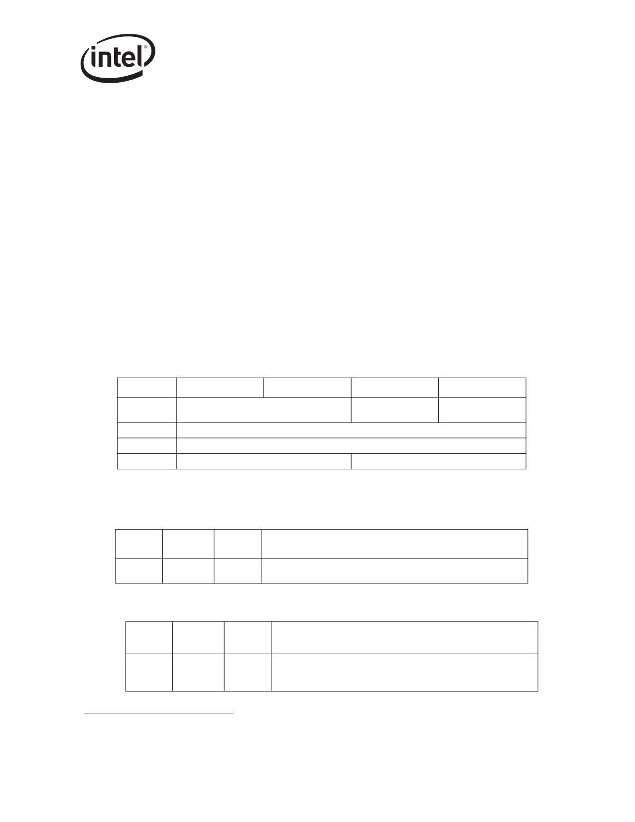
Table 4-4. Status Register Layout
15
4 3
0
Status Bits
Reserved
Bit(s)
Initial Value
Description
3:0
0b
Reserved.
2:0a
Interrupt Status. This bit is 1b when the Ethernet
controller is generating an interrupt internally.
3a
0b
When Interrupt Disable in the Command Register
is also cleared, the Ethernet controller asserts
INTA# or signal an interrupt over CSA.
New Capabilities: Indicates that an Ethernet
controller implements Extended Capabilities. The
Ethernet controller sets this bit and implements a
4
1b
capabilities list to indicate that it supports PCI
Power Management, PCI-X Bus, and message
signaled interrupts.
5
1b
66 MHz Capable (don’t care for the 82547GI/EI).
6
0b
UDF Supported. Hardwired to 0b for PCI 2.3a.
Fast Back-to-Back CapableThis bit must be
7
0b
cleared to 0b in PCI-X mode (not applicable to the
82547GI/EI).
8
0b
Data Parity Reported.
DEVSEL Timing (indicates medium device). Not
10:9
01b
applicable to the 82547GI/EI.
11
0b
Signaled Target Abort.
78
PCI Local Bus Interface
Bit(s)
Initial Value
Description
12
0b
Received Target Abort.
13
0b
Received Master Abort.
Signaled System Error (not applicable to the
14
0b
82547GI/EI).
Detected Parity Error (not applicable to the
15
0b
82547GI/EI).
a.
82541xx and 82547GI/EI only.
4.1.1
PCI-X Configuration Registers
The Ethernet controller supports additional configuration registers that are specific to PCI-X.
These registers are visible in conventional PCI and PCI-X modes, although they only affect the
operation of PCI-X mode. The PCI-X registers are linked into the Capabilities linked list.
Note: The 82540EP/EM, 82541xx, and 82547GI/EI do not support PCI-X mode.
Byte Offset
Byte 3
Byte 2
Byte 1
Byte 0
E4h
PCI-X Command
Next Capability
PCI-X Capability ID
E8h
PCI-X Status
Figure 4-2. PCI-X Capability Registers
4.1.1.1
PCI-X Capability ID
Read/
Initial
Bits
Description
Write
Value
Capability ID - Identifies the PCI-X register set in the capabilities
7:0
R
7
linked list.
4.1.1.2
Next Capability
Read/
Initial
Bits
Description
Write
Value
Next Capability - points to the next capability in the capabilities
7:0
R
F0a
linked list.
a.
In conventional PCI mode, Message Signaled Interrupts can also be disabled in the EEPROM. If disabled, the Message
Signaled Interrupt registers are not visible, and PCI-X’s “Next Capability” pointer is 0b.
79

PCI Local Bus Interface
4.1.1.3
PCI-X Command
15
7
6
4
3
2
1
0
Max. Split Trans-
Read
Reserved
RO
DP
actions
Count
Read
Initial
Bits
Description
Write
Value
Data Parity Error Recovery Enable. If this bit is 1b, the Ethernet
controller attempts to recover from Parity errors. If this bit is 0b, the
0
RW
0b
Ethernet controller asserts SERR# (if enabled) whenever the Master
Data Parity Error bit (Status Register, bit 8) is set.
Enable Relaxed Ordering. If this bit is set, the Ethernet controller sets
1
RW
1b
the Relaxed Ordering attribute bit in some transactions.
Maximum Memory Read Byte Count. This register sets the
maximum byte count the Ethernet controller uses for a Memory Read
Sequence. The allowable values are:
Register
Maximum Byte Count
3:2
RW
0b
0
512
1
1024
2
2048
3
4096
Maximum Outstanding Split Transactions. This register sets the
maximum number of outstanding split transactions that the Ethernet
controller uses. The Ethernet controller is only allowed to have one
outstanding split transaction at any time.
Register
Maximum Outstanding Transactions
0
1
1
2
6:4
RW
0b
2
3
3
4
4
8
5
12
6
16
7
32
15:7
R
0b
Reserved. Reads as 0b
80

PCI Local Bus Interface
4.1.1.4
PCI-X Status
31 29
28 26
25 23
22 21
20
19
18
17
16
15
8
7
3
2
0
Read
Max.
Rd
Device
Func.
Res.
Cplx
USC
SCD
133
64b
Bus Number
Size
Split
Byte
Number
Num.
Read/
Intial
Bits
Description
Write
Value
Function Number. This number forms part of the Requester and
2:0
R
0b
Completer IDs for PCI-X transactions.
Device Number. The system assigns a device number (other than 0b) to
the Ethernet controller. It forms part of the Requester and Completer IDs
7:3
R
1Fh
for PCI-X transactions. The Ethernet controller updates this register with
the contents of AD[15:11] on any Type 0 Configuration Write cycle.
Bus Number. This indicates the bus the Ethernet controller is placed on. It
forms part of the Requester and Completer IDs for PCI-X transactions. The
15:8
R
FFh
Ethernet controller updates this register with the contents of AD[7:0] on any
Type 0 Configuration Write cycle.
64-bit Device. This indicates the Ethernet controller is a 64-bit device. It
16
R
1ba
does not indicate the current bus width. It is loaded from the EEPROM
Initialization Control Word 2 (see Section 5.6.12).
133 MHz Capable. A 1b indicates that the Ethernet controller is capable of
operating at 133 MHz in PCI-X mode. A 0b indicates 66 MHz capability.
17
R
1ba
This bit is loaded from the EEPROM Initialization Control Word 2 (see
Section 5.6.12).
Split Completion Discarded. (Write 1b to clear) This bit is set if the
read, write 1b
18
0b
Ethernet controller discards a Split Completion because the requester
to clear
would not accept it.
Unexpected Split Completion. (Write 1b to clear) This bit indicates
read, write 1b
19
0b
whether the Ethernet controller received an unexpected Split Completion
to clear
with its requestor ID.
Device Complexity. A 0b indicates the Ethernet controller is a simple
20
R
0b
device. A 1b indicates that the Ethernet controller is a bridge.
Designed Maximum Memory Read Byte Count. Indicates the maximum
memory read byte count the Ethernet controller is designed to generate.
Register
Maximum Byte Count
0
512
1
1024
22:21
R
2ba
2
2048
3
4096
The value of this register depends on the Max_Read bit in the EEPROM’s
Initialization Control Word 2 (see Section 5.6.12).
Max_Read = 0b then value = 2 (2 KB)
Max_Read = 1b then value = 3 (4 KB)
81

PCI Local Bus Interface
Read/
Intial
Bits
Description
Write
Value
Designed Maximum Outstanding Split Transactions. A 0b indicates that
the Ethernet controller is designed to have at the most one outstanding
transaction.
Register
Maximum Outstanding Transactions
0
1
1
2
25:23
R
0b
2
3
3
4
4
8
5
12
6
16
7
32
Designed Maximum Cumulative Read Size. Indicates a number that is
greater or equal maximum cumulative outstanding bytes to be read at one
time.
Register
Maximum Outstanding Bytes
0
1 KB
1
2 KB
2
4 KB
3
8 KB
4
16 KB
5
32 KB
6
64 KB
7
128 KB
28:26
R
The value of this register depends on the DMCR_Map and Max_Read bits
in the EEPROM’s Initialization Control Word 2 (see Section 5.6.12).
• DMCR_Map = 0b:
The value of this register reflects the number of bytes programmed in the
Maximum Memory Read Byte Count (MMRBC) field of the PCI-X
Command Register as follows:
• MMRBC = 0 (512) - DMCRS = 0 (1KB)
• MMRBC = 1 (1K) - DMCRS = 0 (1KB)
• MMRBC = 2 (2K) - DMCRS = 1 (2KB)
• MMRBC = 3 (4K) - DMCRS = 2 (4KB)
• DMCR_Map = 1b and Max_Read = 0b: DMCRS = 1 (2KB)
• DMCR_Map = 1b and Max_Read = 1b: DMCRS = 2 (4KB)
Received Split Completion Error Message. This bit is set if the Ethernet
Read, write 1b
29
0b
controller receives a Split Completion Message with the Split Completion
to clear
Error attribute bit set.
31:30
R
0b
Reserved. Reads as 0b
a. Loaded from EEPROM.
4.1.2
Reserved and Undefined Addresses
Any PCI or PCI-X register address space not explicitly declared in this specification should be
considered to be reserved, and should not be written. Writing to reserved or undefined
configuration register addresses can cause indeterminate behavior. Reads from reserved or
undefined configuration register addresses can return indeterminate values.
82
PCI Local Bus Interface
4.1.3
Message Signaled Interrupts1
Message Signaled Interrupt (MSI) capability is optional for PCI 2.2 or 2.3, but required for PCI-X.
When Message Signaled Interrupts are enabled, instead of asserting an interrupt pin, the Ethernet
controller generates an interrupt using a memory write command. The address and most of the data
of the command are determined by the system and programmed in configuration registers. This
permits the system to program a different message for each function so it can speed up interrupt
delivery.
To enable Message Signaled Interrupts, the system software writes to the “MSI Enable” bit in the
MSI “Message Control” register. When Message Signaled Interrupts are enabled, the Ethernet
controller no longer asserts its INTA# pin to signal interrupts.
MSI systems allow a function to request up to 32 messages, but does not guarantee that all of them
are allocated. The Ethernet controller supports only a single message. When Message Signaled
Interrupts are enabled, the Ethernet controller generates a message when any of the unmasked bits
in the Interrupt Cause Read register (ICR) are set to 1b. The Ethernet controller does not generate
the message again until the ICR is read and a subsequent interrupt event occurs.
In conventional PCI mode, Message Signaled Interrupts can also be disabled in the EEPROM. If
MSI is disabled, the Message Signaled Interrupt registers is not visible.
4.1.3.1
Message Signaled Interrupt Configuration Registers
Byte Offset
Byte 3
Byte 2
Byte 1
Byte 0
MSI
F0h
Message Control
Next Capability
Capability ID
F4h
Message Address
F8h
Message Upper Address
FCh
Reserved
Message Data
Figure 4-3. Message Signaled Interrupt Configuration Registers
4.1.3.1.1
MSI Capability ID
Read/
Initial
Bits
Description
Write
Value
Capability ID - Identifies the Message Signaled Interrupt register set in
7:0
R
05h
the capabilities linked list.
4.1.3.1.2
Next Capability
Read/
Initial
Bits
Description
Write
Value
Next Capability - points to the next capability in the capabilities
7:0
R
00h
linked list. Its value is 0b since the Message Signaled Interrupt is the
last item in the list.
1.
Not applicable to the 82541xx or 82547GI/EI.
83
PCI Local Bus Interface
4.1.3.1.3
Message Control
15
8
7
6
4
3
1
0
Multiple
Multiple
Reserved
64b
En
Enable
Capable
Read/
Initial
Bits
Description
Write
Value
MSI Enable. If 1b, Message Signaled Interruptsa are enabled and the
0
R
0b
Ethernet controller generates Message Signaled Interrupts instead of
asserting INTA#.
Multiple Message Capable. Indicates the number of messages
requested. The Ethernet controller only requests one message.
Register
Number of messages
0
1
1
2
2
4
3:1
R
0b
3
8
4
16
5
32
6
Reserved
7
Reserved
Multiple Message Enable. Written by the system to indicate the
number of messages allocated. Since the Ethernet controller only
6:4
RW
0b
supports one message, the system should never write a value other
than 0b.
64-bit capable. A value of 1b indicates that the Ethernet controller is
7
R
1b
capable of generating 64-bit message addresses.
15:8
R
0b
Reserved. Reads as 0b.
a.
Not applicable to the 82541xx or 82547GI/EI.
84

PCI Local Bus Interface
4.1.3.1.4
Message Address
Read/
Initial
Bits
Description
Write
Value
Message Address - Written by the system to indicate the lower 32-
31:0
RW
0b
bits of the address to use for the MSI memory write transaction. The
lower two bits are always written as 0b.
4.1.3.1.5
Message Upper Address
Read/
Initial
Bits
Description
Write
Value
Message Upper Address - Written by the system to indicate the
31:0
RW
0b
upper 32-bits of the address to use for the MSI memory write
transaction.
4.1.3.1.6
Message Data
Read/
Initial
Bits
Description
Write
Value
Message Data - Written by the system to indicate the lower 16 bits of
15:0
RW
0b
the data written in the MSI memory write DWORD transaction. The
upper 16 bits of the transaction are written as 0b.
4.2
Commands
The Ethernet controller is capable of decoding and encoding commands for both PCI and PCI-X
modes. The difference between PCI and PCI-X commands is noted in Table 4-5.
Table 4-5. PCI and PCI-X Encoding Difference
C/BE
PCI Commands
Abr.
PCI-X Commands
Abr.
Encoding
0h
Interrupt Acknowledge
Interrupt Acknowledge
1h
Special Cycle
Special Cycle
2h
I/O Read
IOR
I/O Read
IOR
3h
I/O Write
IOW
I/O Write
IOW
4h
Reserved
Reserved
5h
Reserved
Reserved
6h
Memory Read
MR
Memory Read DWORD
MRD
7h
Memory Write
MW
8h
Reserved
Alias to MRB
AMR
9h
Reserved
Alias to MWB
AMW
Ah
Configuration Read
CFR
Configuration Read
CFR
Bh
Configuration Write
CFW
Configuration Write
CFW
Ch
Memory Read Multiple
MRM
Split Completion
SC
85
PCI Local Bus Interface
Table 4-5. PCI and PCI-X Encoding Difference
C/BE
PCI Commands
Abr.
PCI-X Commands
Abr.
Encoding
Dh
Dual Address Cycle
DAC
Dual Address Cycle
DAC
Eh
Memory Read Line
MRL
Memory Read Block
MRB
Fh
Memory Write & Invalidate
MWI
Memory Write Block
MWB
As a target, the Ethernet controller only accepts transactions that address its BARs or a
configuration transaction in which its IDSEL input is asserted. In PCI-X mode, the Ethernet
controller also accepts split completion for an outstanding memory read command that it has
requested. The Ethernet controller does not respond to Interrupt Acknowledge or Special Cycle in
either mode.
Table 4-6. Accepted PCI/PCI-X Command as a Target
Transaction Target
PCI Commands
PCI-X Commands
Register or Flash Read
MR,MRL,MRM,IOR
MRD, MRB, AMR,IOR
Register or Flash Write
MW, MWI,IOW
MW, MWB, AMW,IOW
Configuration Read
CFR
CFR
Configuration Write
CFW
CFW
Memory Read Completion
N/A
SC
As a master, the Ethernet controller generates Read and Write commands for different causes as
listed in Table 4-7. The addresses of these transactions are programmed either by system software
or the software driver. The Ethernet controller always expects that they are claimed by one of the
devices on the bus segment. The Ethernet controller never generates Interrupt Acknowledge,
Special Cycle, I/O commands, or Configuration Commands.
Table 4-7. Generated PCI/PCI-X as a Master
Transaction Cause
PCI Commands
PCI-X Commands
CMD
RO
Tx Descriptor Read
MR,MRL,MRM
MRB
1
Tx Descriptor Write back
MW,MWI
MWB
0
Tx Data Read
MR, MRL,MRM
MRB
1
Rx Descriptor Read
MR,MRL,MRM
MRB
1
Rx Descriptor Write back
MW,MWI
MWB
0
Rx Data Write
MW,MWI
MWB
1
Message Signaled Interrupta
MW
MWB
0
Split Completion
N/A
SC
N/A
a.
Not applicable to the 82541xx or 82547GI/EI.
Transaction burst length on PCI is determined by several factors, including the PCI latency timer
expiration, the type of bus transfer (descriptor read/write or data read/write) made, the size of the
data transfer (for data transfers), and whether the cycle is initiated by the receive or transmit logic.
86
PCI Local Bus Interface
Following are a few specific rules:
• For descriptor fetches, the burst length is always equal to the multiple of cache line sizes set by
the transmit and receive descriptor fetch threshold fields. (See Section 3.2.4 and Section 3.4.1)
For descriptor writes, the transfer size ranges from 8 bytes to N cache line's worth of data.
Cache line sizes are: 16, 32, 64, and 128 bytes.
• For transmit data fetches, the burst length is generally equal to the block of data being fetched,
in other words, a descriptor's worth of data.
• For receive data writes, the burst size is typically equal to the packet length (rounded up to the
next 8 bytes) or the buffer size, whichever is smaller.
4.3
PCI/PCI-X Command Usage
The Ethernet controller optimizes the use of PCI/PCI-X bus cycles to maximize throughput. The
following sections describe this behavior.
4.3.1
Memory Write Operations
Memory write command usage has been implemented in the Ethernet controller to improve PCI
performance. As noted below, cache line size has a significant impact on the usage of memory
write commands. Specifically, cache line size entries which are unsupported causes hardware to
default to the Memory Write (MW) command for all master write transactions. Also, all writes
default to MW if the Memory Write and Invalidate (MWI) enable bit in the PCI configuration
command register is 0b. MWI is the preferred write command and is used when the circumstances
allow it.
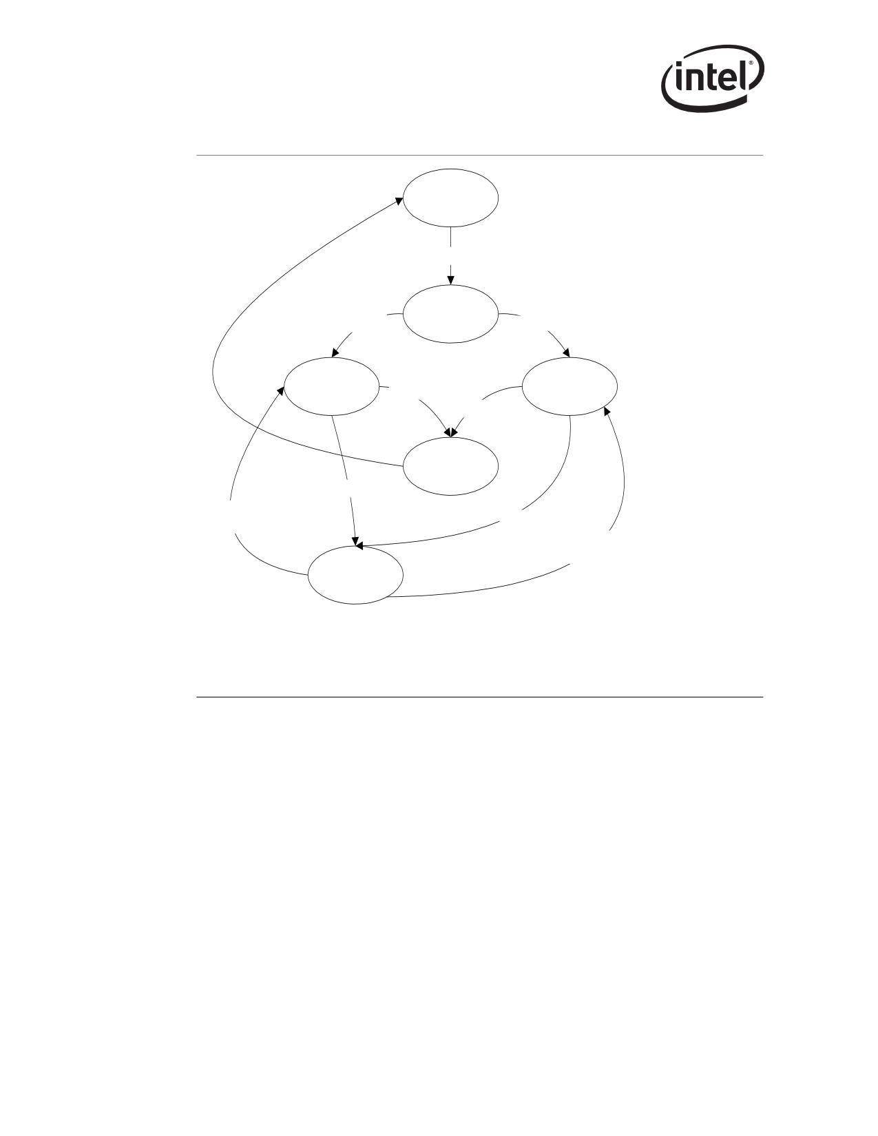
Figure 4-4 depicts a behavioral state-machine representation of the command usage algorithm for
master write operations.
Upon EACH master write access, the hardware evaluates the address alignment and the amount of
data to be transferred. The following guidelines are used for command determination:
• If the address is cache line aligned and there is at least one cache line of data, then hardware
uses the MWI command.
• If the address is aligned but there is not at least one cache line of data, or the address is not
aligned, or if the MWI enable bit is set to 0b, then hardware uses the MW command.
During the burst, regardless of which command was originally issued, the hardware evaluates the
remaining amount of data each time the write burst comes to a cache line boundary, or when the
transaction is terminated due to a target disconnect or latency timer expiration.
87
PCI Local Bus Interface
IDLE
Wr_Req || (Cnt_Rmn != 0)
Write Command
Aligned && (Count >= CLS)
Determination
!Aligned || (Aligned && (Count < CLS)) || !MWI_Enable
MWI
MW
Burst*
Cnt_Rmn = 0
Burst
Cnt_Rmn = 0
Terminate
Transaction
Boundary || Terminate
MWI_Enable &&
Terminate
d && Cnt_Rmn >= CLS)
!MWI_Enable ||
(!Aligned || Cnt_Rmn < CLS)
MWI
Boundary
Evaluation
Count = Amount of data for XFR
Cnt_Rmn = Remaining data for XFR
Wr_Req = Initial request for master write
CLS = Cache line size
* Either the initiation or continuation of the MWI Burst
Boundary = At cache line boundary?
Aligned = Address aligned to cache line boundary
Terminate = Target disconnect or latency timer e
Figure 4-4. Master Write Command Usage Algorithm
4.3.1.1
MWI Bursts
• If there is at least one cache line of data remaining, then the Ethernet controller continues the
MWI burst.
• If there is not at least one cache line of data remaining, then the Ethernet controller terminates
the transaction on the boundary, re-acquires the bus, and issues a MW command for the
remainder of data.
• If the transaction is terminated prematurely due to a target disconnect or latency time-out, the
Ethernet controller re-evaluates command usage based on the new start address and the
amount of remaining data.
88
PCI Local Bus Interface
4.3.1.2
MW Bursts
• The Ethernet controller always continues the burst until the end. If the system is concerned
about MWI usage, it disconnects at the cache line boundary. The Ethernet controller then
restarts the transaction and re-evaluates command usage.
Note: The algorithm described above defaults to the MW case when the MWI enable bit in the
Configuration Register is set to 0b.
4.3.2
Memory Read Operations
For all read commands, the hardware evaluates the amount of data to be read with respect to the
cache line size register and the read address alignment for command determination. The following
rules apply:
Table 4-8. Rules for Memory Read Operations
Amount of
Number of Cache Line
Command
Data Requested
Boundaries Crossed
Used by Hardware
> 2 Cache Lines
n/a
MRM
>= 1 Cache Line
>= 2
MRM
<= 1 Cache Line
0 or 1
MRL
< 1 Cache Line
0
MR
In other words, read command usage depends on the number of cache lines from which the data
must be read from the target device.
As mentioned above, unsupported values in the cache line size field default to a size of 32 bytes for
the memory read command usage algorithm.
Note: MRL should be used for a single cache line of data that is cache line aligned.
4.3.2.1
PCI-X Command Usage
In PCI-X mode, the Ethernet controller takes advantage of split transaction protocol to minimize
retries and eliminate delayed read transactions.
Target Split Responses
When the Ethernet controller responds to a Memory Read or I/O Read command it determines if
the data can be returned within 16 clock cycles. If not, it signals a split response and returns data
later through the split completion protocol. If the Ethernet controller already has a command in its
completion register it retries the requested read until the register is empty. Target posted writes and
split completion are still accepted during that period. The internal register reads that cause splits
are:
• General Registers: CTRL, STATUS, EECD, CTRL_EXT, FCAL, FCAH, FCT, VET, FCTTV,
TXCW, RXCW, PBA,
• Interrupt Registers: ICR, ICS, IMS, IMC
• Transmit Registers: TCTL
89
PCI Local Bus Interface
Outstanding Memory Read
When the Ethernet controller masters a memory read and is responded to with a split response it
waits for the completion of the data as a target. The Ethernet controller allows one outstanding
memory read command at any time. The Ethernet controller continues to master posted memory
writes and split completions if there are any.
Relaxed Ordering
• The Ethernet controller takes advantage of the relaxed ordering rules in PCI-X. By setting the
RO bit for some of its master transactions, the Ethernet controller allows the system to
optimize performance in the following cases:
- Relaxed ordering for descriptor and data reads: When the Ethernet controller masters a
read transaction its split completion has no relationship with the writes from the CPUs
(same direction). It should be allowed to bypass the writes from the CPUs.
- Relaxed ordering for receiving data writes: When the Ethernet controller masters receive
data writes it also allows them to bypass each other in the path to system memory because
the software does not process this data until their associated descriptor writes are done.
• The Ethernet controller cannot relax ordering for descriptor writes or an MSI write.
No Snoop Setting
The Ethernet controller always clears this bit in all of its master transactions because it cannot
guarantee that the memory locations between transaction addresses are not cached in the system.
4.4
Cache Line Information1
The cache line size PCI configuration register is programmed by the BIOS and/or OS after a
system reset. The value in the cache line size register corresponds to the cache line size that the
system supports.
The value programmed into the cache line size register affects the DMA operations of the Ethernet
controller. In general, the hardware attempts to fetch descriptors on a cache line basis. It also
attempts to write back descriptors when a cache line of descriptors has been filled.
The size of the cache line register also has an effect on the Ethernet controller’s usage of the MWI
PCI command, because the use of this command requires that at least a whole cache line of data is
written. The memory read commands are also affected as discussed in Section 4.3.2.
In PCI-X mode, the cache line size does not affect the commands used. However it does affect the
descriptor transfer. If an unsupported cache line size larger than 128 bytes is programmed, the
Ethernet controller acts as if a cache line size of 128 bytes was programmed.
1.
Not applicable to the 82547GI/EI.
90
PCI Local Bus Interface
4.4.1
Target Transaction Termination
When the Ethernet controller accepts a transaction as a target it always disconnects the transaction
after a single data phase by following the “Master Completion Termination” in PCI 2.2, 2.3, or
“Single data phase disconnect termination” in PCI-X. The “memory” in the Ethernet controller is
actually a set of registers and is marked as “non-prefetchable”. This is also the case for FLASH
memory.
4.5
Interrupt Assignment (82547GI/EI Only)
During a Power-On Self-Test (POST), the system BIOS must assign an Interrupt Request (IRQ) for
the 82547GI(EI). The 82547GI(EI) generates an interrupt by sending a hub interface message
through the CSA port.
In a typical system, the 82547GI(EI) component is Device 1 on the bus behind the CSA bridge
component. When the GMCH component receives an interrupt message, it forwards the interrupt
through a PIRQ programmed into the CSA Interface Interrupt Control Register (CSAINTC). Use
the following information to program this register:
Address Offset - 48h
Default Value - 04h
Access - R/W
Size - 8 bits
Bit Field - [2:1]
Description - PCI Interrupt type for CSA generated Interrupt - R/W
00 - Reserved
01 - INT#B
10 - INT#C (default)
11 - INT#D
Interrupts are communicated with a special CSA bus cycle that causes the MCH to issue an
interrupt to the interrupt controller in the ICH.
4.6
LAN Disable
For LAN designs, it is often desirable to program the BIOS setup to selectively enable or disable
LOM devices. This capability gives the end user more control over system resource management
and avoids conflicts with add-in boards.
Device presence or absence must be established early during BIOS execution to ensure that
resource allocation (interrupts and memory) is performed correctly. This task is frequently
accomplished using a BIOS CVDR (Configuration Values Driven on Reset) mechanism.
The 82541xx and 82547GI/EI LAN disable function resides on the FLSH_SO pin. This pin should
be driven by a port on the system Super IO device so that BIOS can control it dependably.
91
PCI Local Bus Interface
4.7
CardBus Application (82541PI/GI/EI Only)
The 82541PI/GI/EI has some features to facilitate its use in a CardBus application, following
revision 7 of the PC Card specification.
To use the 82541PI/GI/EI on CardBus, an external flash memory is required. Configure the Base
Address Registers to 32-bit (required for CardBus) and enable CLKRUN in EEPROM. Setting
these bits also enables the CardBus Information Space (CIS) pointer in the PCI Configuration
Space. When enabled, the CIS pointer starts the first tuple of the CIS chain at byte address 20h in
the Flash device. The PC Card specification requires that this tuple be a CISTPL_LINKTARGET
tuple. The tuple chain can then continue within the memory.
When operating as a CardBus card, the 82541PI/GI/EI supports full functionality with the
exception of wake up.
92
EEPROM Interface
5
5.1
General Overview
The PCI/PCI-X Family of Gigabit Ethernet Controllers uses an EEPROM device for storing
product configuration information. The EEPROM is divided into four general regions:
• Hardware accessed - loaded by the Ethernet controller after power-up, PCI Reset
deassertion, D3->D0 transition, or software commanded EEPROM reset
(CTRL_EXT.EE_RST).
• ASF accessed - loaded by the Ethernet controller in ASF mode after power-up, ASF Soft
Reset (ASF FRC_RST), or software commanded ASF EEPROM read (ASF FRC_EELD).
• Software accessed - used by software only. The meaning of these registers as listed here is a
convention for the software only and is ignored by the Ethernet controller.
• External BMC (TCO) accessed - loaded by an external BMC (TCO) from the SMBus after
power up.
Note: The 82544GC/EI and 82541ER do not support ASF, SMBus, or an external BMC (TCO).
Several words of the EEPROM are accessed automatically by the Ethernet controller after reset to
provide pre-boot configuration data before it is accessed by host software. The remainder of the
stored information is available to software for storing the MAC address, serial numbers, and
additional configuration information.
Intel has a software utility called EEUPDATE, which can be used to program EEPROM images in
development or production line environments. To obtain a copy of this program, contact your Intel
representative.
Note: Since the 82546GB/EB is a dual port device, there are portions of the EEPROM and Flash that
control one or both ports. Special considerations due to this feature are noted in this section.
93
EEPROM Interface
5.2
Component Identification Via Programming
Interface
Ethernet controller stepping is identified by the following register contents.
Table 5-1. Component Identification
Stepping
Vendor ID
Device ID
Description
82547EI-A0
8086h
1019h
Copper
82547EI-A1
8086h
1019h
Copper
82547EI-B0
8086h
1019h
Copper
82547EI-B0
8086h
101Ah
Mobile
82547GI-B0
8086h
1019h
Copper
Copper; Dual Port
82546EB-A1
8086h
1010h
MAC Default
82546EB-A1
8086h
1012h
Fiber; Dual Port
82546EB-A1
8086h
101Dh
Copper; Quad Port
82546GB-B0
8086h
1079h
Copper; Dual Port
82546GB-B0
8086h
107Ah
Fiber; Dual Port
82546GB-B0
8086h
107Bh
SerDes; Dual Port
82545EM-A
8086h
100Fh
Copper
82545EM-A
8086h
1011h
Fiber
Copper
82545GM-B
8086h
1026h
MAC Default
82545GM-B
8086h
1027h
Fiber
82545GM-B
8086h
1028h
SerDes
Copper
82544EI-A4
8086h
1107h
MAC Default
Copper
82544GC-A4
8086h
1112h
MAC Default
Cooper
82541EI-A0
8086h
1013h
MAC Default
Cooper
82541EI-A0
8086h
1013h
MAC Default
Cooper
82541EI-B0
8086h
1013h
MAC Default
82541EI-B0
8086h
1018h
Mobile
94

EEPROM Interface
Table 5-1. Component Identification
Stepping
Vendor ID
Device ID
Description
82541GI-B1
8086h
1076h
Cooper
82541GI-B1
8086h
1077h
Mobile
82541PI-C0
8086h
1076h
Cooper
82541ER-C0
8086h
1078h
Cooper
82540EP-A
8086h
1017
Desktop
82540EP-A
8086h
1016
Mobile
82540EM-A
8086h
100E
Desktop
82540EM-A
8086h
1015
Mobile
Note: These Ethernet controllers also provide identification data through the Test Access Port (TAP).
5.3
EEPROM Device and Interface
The EEPROM access algorithm, programmed into the Ethernet controller, is compatible with most,
but not all, commerically available 3.3 V dc Microwire* interfaces and serial EEPROM devices
with a 1 MHz speed rating. Ethernet controllers are compatible with two sizes of 4-wire serial
EEPROM devices1. If ASF mode functionality is desired, a 4096-bit serial NM93C66 compatible
EEPROM can be used. Otherwise, a 1024-bit serial NM93C46 compatible EEPROM can be used.
Both EEPROMs are accessed in 16-bit words; the larger has 256 words while the smaller has 64
words. Refer to the appropriate Ethernet controller’s design guide for recommended EEPROM
manufacturers.
An Ethernet controller automatically determines which EEPROM it is connected to and sets the
EEPROM SIZE field of the EEPROM/FLASH Control and Data Register (EEC.EE_SIZE) field
appropriately. Software can use this field to determine how to access the EEPROM using direct
access. Note that different EEPROM sizes have different numbers of address bits and therefore
must be accessed with a slightly different serial protocol. Software must be aware of this if it
accesses the EEPROM using direct access.
1.
The 82544GC/EI only supports one size of EEPROM. Refer to the 82544GC Gigabit Ethernet Controller Datasheet and Hardware Design
Guide (AP-427) for more information.
95
EEPROM Interface
The EEPROM interface trace routing is not critical because the interface runs at a very slow speed.
Note: For the 82544GC/EI, 82540EP/EM, 82541xx, and 82547GI/EI, the EEPROM access algorithm
drives extra pulses on the shift clock at the beginnings and ends of read and write cycles. the extra
pulses might violate the timing specifications of some EEPROM devices. In selecting a serial
EEPROM, choose a device that specifies “don’t care” shift clock states between accesses.
5.3.1
Software Access
The Ethernet controller provides two different methods for software access to the EEPROM.
Software can either use the built-in controller to read the EEPROM, or access the EEPROM
directly using the EEPROM’s 4-wire interface.
Software can use the EEPROM Read register (EERD) to cause the Ethernet controller to read a
word from the EEPROM that the software can then use. To do this, software writes the address to
read the Read Address (EERD.ADDR) field and then simultaneously writes a 1b to the Start Read
bit (EERD.START). The Ethernet controller then reads the word from the EEPROM, sets the Read
Done bit (EERD.DONE), and puts the data in the Read Data field (EERD.DATA). Software can
poll the EEPROM Read register until it sees the EERD.DONE bit set, then use the data from the
EERD.DATA field. Any words read this way are not written to hardware’s internal registers.
Software can also directly access the EEPROM’s 4-wire interface through the EEPROM/FLASH
Control Register (EEC). It can use this for reads, writes, or other EEPROM operations.
To directly access the EEPROM, software should follow these steps:
1. Write a 1b to the EEPROM Request bit (EEC.EE_REQ).
2. Read the EEPROM Grant bit (EEC.EE_GNT) until it becomes 1b. It remains 0b as long as the
hardware is accessing the EEPROM.
3. Write or read the EEPROM using the direct access to the 4-wire interface as defined in the
EEPROM/FLASH Control & Data Register (EEC). The exact protocol used depends on the
EEPROM placed on the board and can be found in the appropriate data sheet.
4. Write a 0b to the EEPROM Request bit (EEC.EE_REQ).
Software can cause the Ethernet controller to re-read the hardware accessed fields of the EEPROM
(setting hardware’s internal registers appropriately) by writing a 1b to the EEPROM Reset bit of
the Extended Device Control Register (CTRL_EXT.EE_RST). This action will also cause a reset.
5.4
Signature and CRC Fields
The Ethernet controller uses the Signature and CRC fields to determine if an EEPROM is present
by attempting to read the EEPROM. The Ethernet controller first reads the Initialization Control
Word 1 at address 0Ah and then checks the received value for bits 15 and 14. If bit 15 is 0b and bit
14 is 1b, the Ethernet controller considers the EEPROM to be present and valid. It then reads the
additional EEPROM words and programs its internal registers based on the values read. Otherwise,
it ignores the values it read from the Initialization Control Word 1 and does not read any other
words.
96
EEPROM Interface
In ASF Mode1, the Ethernet controller's ASF function reads the ASF CRC word to determine if the
EEPROM is valid. If the CRC is not valid, the ASF Configuration registers retain their default
value. This CRC does not affect any of the remaining Ethernet controller's configuration, including
the Management Control Register.
5.5
EEUPDATE Utility
The EEUPDATE utility meets the two basic requirements for an in-circuit programming utility.
First, the utility can be used to update EEPROM images as part of an end-of-line production tool.
Secondly, it can be used as a standalone development tool. The tool uses the two basic data files
outlined in the following section (static data file and IA address file). To obtain a copy of this
program, contact your Intel representative.
The EEUPDATE utility is flexible and can be used to update the entire EEPROM image or update
only the IA address of the Ethernet controller.
5.5.1
Command Line Parameters
The DOS command format is a follows:
EEUPDATE Parameter_1 Parameter_2
where:
Parameter_1 = filename or /D
Parameter_2 = filename or /A
Parameter 1, above, is file1.eep, which contains the complete EEPROM image in a
specific format that is used to update the complete EEPROM. All comments in the .eep file must
be preceded by a semicolon (;).
Parameter 1 can also be a switch /D. the switch /D implies: do not update the complete
EEPROM image.
Parameter 2, above, is file2.dat, which contains a list of IA addresses. the EEUPDATE
utility picks up the first unused address from this file and uses it to update the EEPROM. An
address is marked as used by following the address with a date stamp. When the utility uses a
specific address, it updates that address as used in a log file called eelog.dat. This file should then
be used as the .dat file for the next update.
Note: Refer to the appropriate Ethernet controller’s EEPROM map and programming information for
sample EEPROM images.
1.
The 82544GC/EI and 82541ER do not support ASF.
97

EEPROM Interface
5.6
EEPROM Address Map1
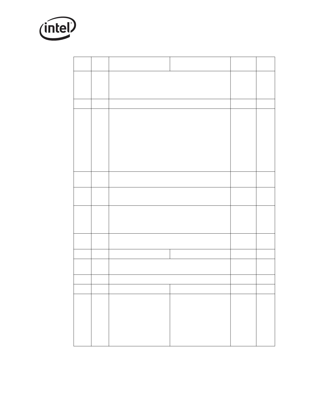
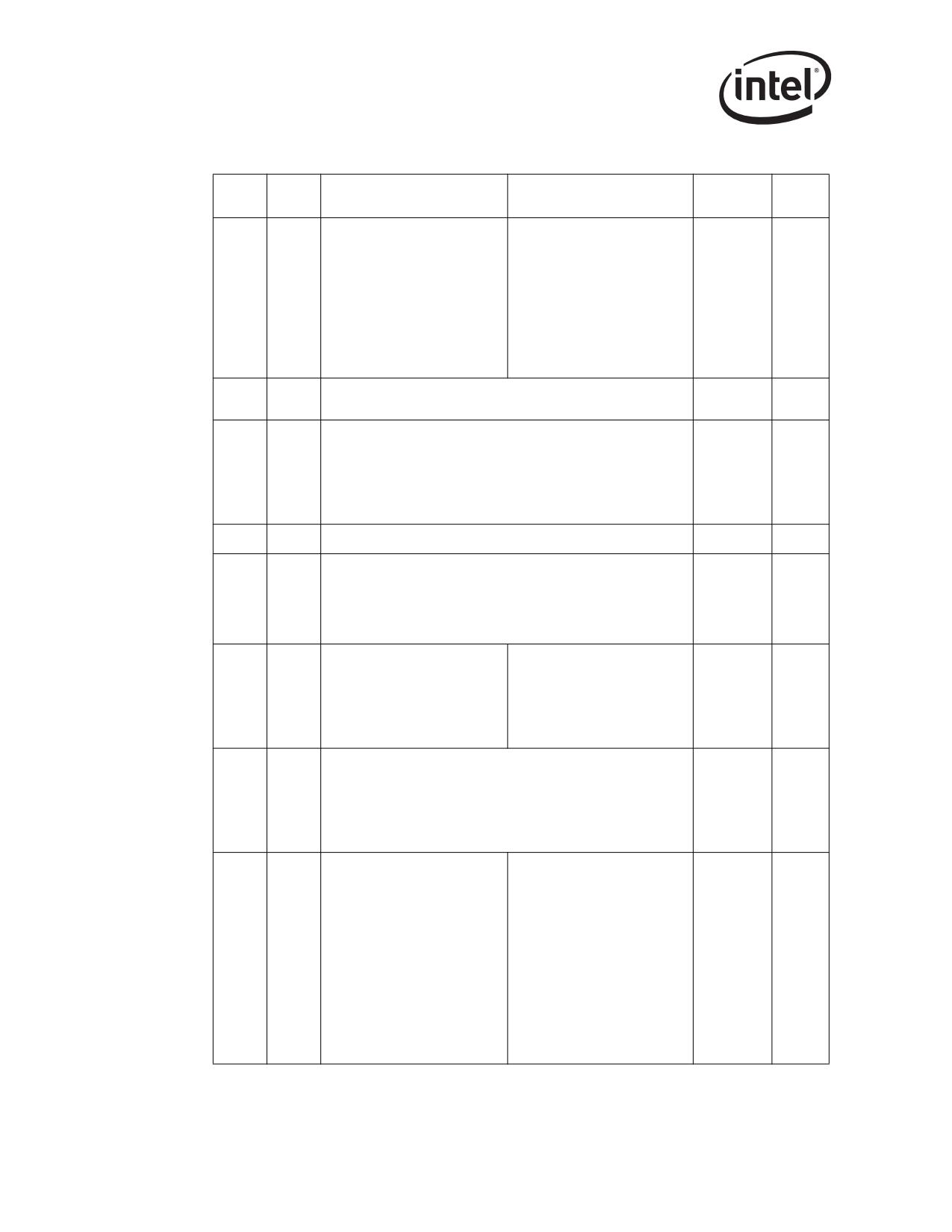
Table 5-2 lists the EEPROM address map for the Ethernet controllers. Each word listed is
described in the sections that follow.
Note: The “LAN A/B” column in Table 5-2 is only applicable to the 82546GB/EB.
Table 5-2. Ethernet Controller Address Map
Used
Bit
Bit
Image
LAN
Word
By
15 - 8
7 - 0
Value
A/B
00h
HW
Ethernet Address Byte 2
Ethernet Address Byte 1
IA(2,1)
LAN
01h
HW
Ethernet Address Byte 4
Ethernet Address Byte 3
IA(4,3)
A/B
(both)
02h
HW
Ethernet Address Byte 6a
Ethernet Address Byte 5
IA(6,5)
03h
Compatibility High
Compatibility Low
0000h
both
SerDes Configuration
04h
SW
Note: Not applicable to the 82540EP/EM, 82541xx, and
FFFFh
both
82547GI/EI
EEPROM Image Version
05h
SW
0000h
N/A
Note: Applicable to the 82541xx and 82547GI/EI only
Compatibility High
Compatibility Low
05h
0000h
(Words 06h and 07h reserved
(Words 06h and 07h reserved
06h
0000h
both
for the 82541xx and 82547GI/
for the 82541xx and 82547GI/
07h
0000h
EI)
EI)
08h
PBA, byte 1
PBA, byte 2
09h
PBA, byte 3
PBA, byte 4
4408h
640Ah for
0Ah
HW
Init Control 1
both
the
82541xx
and
82547GI/EI
see Table
5-1 for
0Bh
HW
Subsystem ID (Vendor)
specific
both
image
values
0Ch
HW
Subsystem Vendor ID
8086h
both
1.
Refer to Table 5-3 for the 82544GC/EI and 82541ER EEPROM address map.
98
EEPROM Interface
Table 5-2. Ethernet Controller Address Map
Used
Bit
Bit
Image
LAN
Word
By
15 - 8
7 - 0
Value
A/B
see Table
5-1 for
0Dh
HW
Device ID
specific
LAN A
image
values
0Eh
HW
Vendor ID
8086h
both
3040h for
the
82545GM/
EM and
82540EP/
EM
0Fh
HW
Init Control 2
both
B080h for
the
82541xx
and
82547GI/EI
10h
PHY Registers
00BAh
SW
N/A
11h
82541xx and 82547GI/EI only
0000h
Software Defined Pins Control (82546GB/EB only)
10h
HW
Note: Words 10h, 11h, and 13h through 1Fh are reserved for the
XXXXh
LAN B
82545GM/EM and 82540EP/EM
see Table
5-1 for
Device ID
11h
HW
specific
LAN B
82546GB/EB only
image
values
EEPROM Size
12h
HW
N/A
82541xx and 82547GI/EI only
12h
HW
Common Power
both
13h
PHY Registers
00BAh
SW
N/A
1Eh
82541xx and 82547GI/EI only
0000h
13h
HW
Management Control
LAN B
14h
HW
Init Control 3
SMBus Addressb
XXXXh
LAN B
15h
IPv4 Address Byte 2
IPv4 Address Byte 1
IP(2,1)
HW
LAN B
16h
IPv4 Address Byte 4
IPv4 Address Byte 3
IP(4,3)
99
EEPROM Interface
Table 5-2. Ethernet Controller Address Map
Used
Bit
Bit
Image
LAN
Word
By
15 - 8
7 - 0
Value
A/B
17h
IPv6 Address Byte 2
IPv6 Address Byte 1
IP(2,1)
18h
IPv6 Address Byte 4
IPv6 Address Byte 3
IP(4,3)
19h
IPv6 Address Byte 6
IPv6 Address Byte 5
IP(6,5)
1Ah
IPv6 Address Byte 8
IPv6 Address Byte 7
IP(8,7)
HW
LAN B
1Bh
IPv6 Address Byte 10
IPv6 Address Byte 9
IP(10,9)
1Ch
IPv6 Address Byte 12
IPv6 Address Byte 11
IP(12,11)
1Dh
IPv6 Address Byte 14
IPv6 Address Byte 13
IP(14,13)
1Eh
IPv6 Address Byte 16
IPv6 Address Byte 15
IP(16,15)
CSA Port Config 1 (82547GI/EI only)
1Fh
0000h
N/A
Note: This word is reserved for all remaining Ethernet controllers
XXXXh
000Ch for
the
20h
HW
Software Defined Pins Control
LAN A
82541xx
and
82547GI/EI
21h
HW
CSA Port Config 2 (82547GI/EI only)
0002h
N/A
7863h
7061h for
21h
HW
Circuit Control
the
both
82540EP/
EM
280Ch
280Bh for
the
22h
HW
D0 Power
D3 Power
both
82541xx
and
82547GI/EI
XXC8h
XXXXh for
the
23h
HW
Management Control
LAN A
82541xx
and
82547GI/EI
XXXXh
XXC8h for
the
82545GM/
EM and
82540EP/
24h
HW
Init Control 3
SMBus Addressb
EM
LAN A
001Ch for
the
82541xx
and
82547GI/EI
100

EEPROM Interface
Table 5-2. Ethernet Controller Address Map
Used
Bit
Bit
Image
LAN
Word
By
15 - 8
7 - 0
Value
A/B
25h
IPv4 Address Byte 2
IPv4 Address Byte 1
IP(2,1)
HW
LAN A
26h
IPv4 Address Byte 4
IPv4 Address Byte 3
IP(4,3)
27h
IPv6 Address Byte 2
IPv6 Address Byte 1
IP(2,1)
28h
IPv6 Address Byte 4
IPv6 Address Byte 3
IP(4,3)
29h
IPv6 Address Byte 6
IPv6 Address Byte 5
IP(6,5)
2Ah
IPv6 Address Byte 8
IPv6 Address Byte 7
IP(8,7)
HW
LAN A
2Bh
IPv6 Address Byte 10
IPv6 Address Byte 9
IP(10,9)
2Ch
IPv6 Address Byte 12
IPv6 Address Byte 11
IP(12,11)
2Dh
IPv6 Address Byte 14
IPv6 Address Byte 13
IP(14,13)
2Eh
IPv6 Address Byte 16
IPv6 Address Byte 15
IP(16,15)
2Fh
HW
LEDCTL Default
0602h
both
Intel Boot Agent Configuration
30h
31h
32h
Firm-
33h
…
ware
34h
Note: Words 34h and 35h are not applicable to the 82545GM/EM
and 82540EP/EM
3Eh
3Fh
Software Checksum, words 00h through 3Fh
40h
ASF
Controlled by the ASF Agent
F7h
F8h
Free for Software
FFh
a.
The lower bit of the last byte is complemented for LAN B.
b.
The SMBus Address is a 7-bit value that is found in bits 7 through 1 of this byte. Bit 0 should be 0b.
101

EEPROM Interface
Table 5-3. 82544GC/EI and 82541ER EEPROM Address Map
Default
Word
Description
Description
HW Access
Image Value
Address
(Hi Byte)
(Low Byte)
(hex)
00h
Yes
IA Byte 2
IA Byte 1
IA(2,1)
01h
Yes
IA Byte 4
IA Byte 3
IA(4,3)
02h
Yes
IA Byte 6
IA Byte 5
IA(6,5)
03h
No
Compatibility high
Compatibility low
0000h
04h
No
Reserved
0000h
EEPROM Image Version
05h
No
0000h
Note: Word 05h is reserved for the 82544GC/EI
06h
No
Reserved
0000h
07h
08h
No
PBA, byte 1
PBA, byte 2
09h
No
PBA, byte 3
PBA, byte 4
0Ah
Yes
Init Control 1, high byte
Init Control 1, low byte
See Text
Subsystem_ID,
Subsystem_ID,
0Bh
Yes
1005h
high byte
low byte
Subsystem_Vendor,
Subsystem_Vendor,
0Ch
Yes
8086h
high byte
low byte
0Dh
Yes
Device ID, high
Device ID, low
1008h
0Eh
Yes
Vendor ID, high
Vendor ID, low
8086h
0Fh
Yes
Init Control 2, high byte
Init Control 2, low byte
See Text
10h - 1Fh
No
OEM Reserved
OEM Reserved
0000h
Software Defined Pins
Software Defined Pins
20h
Yes
See Text
Control, high byte
Control, low byte
21h
Yes
Circuit Control, high
Circuit Control, low
0021h
22h
Yes
D0 Power
D3 Power
See Text
23h - 2Eh
No
Reserved
Reserved
0000h
LEDCTRL Default
2Fh
Yes
0602h
Note: Word 2Fh is reserved for the 82544GC/EI
Intel Boot Agent
30h - 33h
Firmware
0000h
Note: Words 30 - 33h are reserved for the 82541ER
34h - 3Eh
Fixed
Reserved
Reserved
0000h
Checksum of
3Fh
No
Checksum, high byte
Checksum, low byte
words 00h - 3Eh
102

EEPROM Interface
5.6.1
Ethernet Address (Words 00h-02h)
The Ethernet Individual Address (IA) is a six-byte field that must be unique for each Ethernet port
(and unique for each copy of the EEPROM image). The first three bytes are vendor specific. The
value from this field is loaded into the Receive Address Register 0 (RAL0/RAH0). For a MAC
address of 12-34-56-78-90-AB, words 2:0 load as follows (note that these words are byte-
swapped):
Word 0 = 3412
Word 1 = 7856
Word 2 - AB90
Note: Since the 82546GB/EB is a dual-port device, the Ethernet Address in these words are assigned to
LAN A. The Ethernet Address for LAN B is the Ethernet Address for LAN A with its least
significant bit inverted.
5.6.2
Software Compatibility Word (Word 03h)
This is the third word read by the Ethernet controller and contains additional initialization values
that:
• Sets defaults for some internal registers
• Enables/disables specific features
Note: For the 82544GC/EI, typical values are 0000h for a fiber-based design and 0400h for a copper-
based design.
Table 5-4. Software Compatibility Word (Word 03h)
Bit
Name
Description
15:12
Reserved
Reserved for future use.
LAN on Motherboard (LOM#). Set this bit to 1b (default) to enable LOM#;
11
LOM
set to 0b to disable LOM#.
Server card. Set this bit to 1b (default) to enable server card; set to 0b to
10
SRV
disable server card.
0b is the default setting for the 82541xx and 82547GI/EI.
Client card. Set this bit to 0b (default) to disable client card; set to 1b to
9
CLI
enable client card.
1b is the default setting for the 82541xx and 82547GI/EI.
OEM card. Set this bit to 1b (default) to enable OEM card; set to 0b to
8
OEM
disable OEM card.
7:6
Reserved
Reserved for future use. Set these bits to 0b.
Reserved for future use.
5
Reserved
Set this bit to 1b.
Set this bit to 0b for the 82540EP/EM, 82541xx and 82547GI/EI.
SMBus. Set this bit to 1b (default) to enable SMBus; set to 0b to disable
4
SMBa
SMBus.
103

EEPROM Interface
Table 5-4. Software Compatibility Word (Word 03h)
3
Reserved
Reserved for future use. Set this bit to 0b.
PCI bridge. Set this bit to 0b (default) to disable PCI bridge; set to 1b to
2
BOB
enable PCI bridge.
1b is the default setting for the 82540EP/EM.
1:0
Reserved
Reserved for future use. Set these bits to 0b.
a.
Not applicable to the 82544GC/EI or 82541ER.
5.6.3
SerDes Configuration (Word 04h)
If this word has a value of other than FFFFh, software programs its value into the Extended PHY
Specific Control Register 2, located at address 26d in the PHY register space (see Table 13-47).
Note: SerDes Configuration (Word 04h) is a reserved area for the 82544GC/EI, 82540EP/EM, 82541xx,
and 82547GI/EI.
5.6.4
EEPROM Image Version (Word 05h)
Word 05h determines the EEPROM image version for the 82541xx and the 82547GI/EI.
Bits
Name
Value
15:12
EEPROM major version.
0000h
11:8
EEPROM minor version.
0000h
7:0
EEPROM fix.
00000000h
5.6.5
Compatibility Fields (Word 05h - 07h)
These areas are reserved for compatibility information and are used by software drivers.
5.6.6
PBA Number (Word 08h, 09h)
A nine-digit Printed Board Assembly (PBA) number, used for Intel manufactured adapter cards,
are stored in a four-byte field. Other hardware manufacturers can use these fields as they wish.
Software device drivers should not rely on this field to identify the product or its capabilities.
104

EEPROM Interface
5.6.7
Initialization Control Word 1 (Word 0Ah)
The first word read by the Ethernet controller contains initialization values that:
• Sets defaults for some internal registers
• Enables/disables specific features
• Determines which PCI configuration space values are loaded from the EEPROM
Table 5-5. Initialization Control Word 1 (Word 0Ah)
Bit
Name
Description
The Signature field represents a signature of 01b (default), indicating to the
Ethernet controller that there is a valid EEPROM present.
15:14
Signature
If the Signature field is not 01b, the other bits in this word are ignored, no
further EEPROM read is performed, and default values are used for the
configuration space IDs.
When set to 0b (default), enables 64-bit memory mapping.
13
64/32 BAR
When set to 1b, disables 64-bit memory mapping
Note: Set to 1b for the 82540EP/EM.
When set to 0b (default), does not invert the Power State Output bit 0
(CTRL_EXT[14]).
12
IPS0
When set to 1b, inverts the Power State Output invert bit 0
(CTRL_EXT[14]).
Note: Reserved bit for the 82541xx and 82547GI/EI (set to 0b).
Force Speed bit in the Device Control register (CTRL[11]).
When set to 0b (default), does not force speed.
When set to 1b, forces speed (default for the 82540EP/EM).
11
FRCSPD
For 10/100/1000 Mb/s systems using TBI mode (82544GC/EI)/internal
SerDes (82546GB/EB and 82545GM/EM)a, set this bit to 0b.
Note: Reserved bit for the 82541xx and 82547GI/EI (set to 0b).
Full Duplex (mapped to CTRL[0] and TXCW[5]).
When set to 1b (default), enables full duplex (TBI mode/internal SerDes
only).
10
FD
When set to 0b, disables full duplex (TBI mode only/internal SerDes).
Note: Reserved bit for the 82541PI/GI/EI and 82547GI/EI (set to 1b).
Note: Reserved bit for the 82541ER (set to 0b).
Link Reset (mapped to CTRL[3]).
When set to 0b, enables Auto-Negotiation at power up or when asserting
RST# without driver intervention.
9
LRST
When set to 1b, disables Auto-Negotiation at power up or when asserting
RST# without driver intervention.
Note: Reserved bit for the 82541xx and 82547GI/EI (set to 0b).
When set to 0b (default), does not invert the Power State Output bit 1
(CTRL_EXT[16]).
8
IPS1
When set to 1b, inverts the Power State Output invert bit 1
(CTRL_EXT[16]).
Note: Reserved bit for the 82541xx and 82547GI/EI (set to 0b).
105

EEPROM Interface
Table 5-5. Initialization Control Word 1 (Word 0Ah)
82541xx and 82547GI/EI Only
This bit is used to define the usage of the internal 1.2 V dc and 1.8 V dc
regulators to supply power.
Internal VREG Power
7
Down Control
0b = Yes (default).
1b = No (external regulators used).
Note: Reserved bit for all other Ethernet controllers.
Bit
Name
Description
6:5
Reserved
Reserved for future use. Set these bits to 0b.
4
Reserved
Reserved for copper PHY. Set this bit to 0b.
When set to 1b (default), enables full support for power management.
When set to 0b, the Power Management Registers set is read only. The
3
Power Management
Ethernet controller does not execute a hardware transition to D3.
Note: Reserved bit for the 82541PI/GI/EI and 82547GI/EI (set to 1b).
Note: Reserved bit for the 82541ER (set to 0b).
When set to 0b (default), indicates that the PCICLK is not required for
PME# output.
2
PME Clock
When set to 1b, indicates that the PCICLK is required for PME# output.
Note: Reserved bit for the 82541xx and 82547GI/EI (set to 0b).
When set to 1b (default), indicates that the Ethernet controller is to load its
PCI Subsystem ID and Subsystem Vendor ID from the EEPROM (words
1
Load Subsystem IDs
0Bh, 0Ch).
When set to 0b, indicates that the Ethernet controller is to load the default
PCI Subsystem ID and Subsystem Vendor ID.
When set to 0b (default), indicates that the Ethernet controller is to load the
default values for PCI Vendor and Device IDs.
Load Vendor/Device
0
When set to 1b (default for the 82541xx and 82547GI/EI only), indicates
IDs
that the Ethernet controller is to load its PCI Vendor and Device IDs from
the EEPROM (words 0Dh, 0Eh).
a.
Not applicable to the 82541xx, 82547GI/EI or 82540EP/EM.
5.6.8
Subsystem ID (Word 0Bh)
If the signature bits (15:14) and bit 1 (Load Subsystem IDs) of word 0Ah are valid, this word is
read in to initialize the Subsystem ID.
5.6.9
Subsystem Vendor ID (Word 0Ch)
If the signature bits (15:14) and bit 1 (Load Subsystem IDs) of word 0Ah are valid, this word is
read in to initialize the Subsystem Vendor ID.
106

EEPROM Interface
5.6.10
Device ID (Word 0Dh, 11h1)
If the signature bits (15:14) and bit 1 (Load Subsystem IDs) of word 0Ah are valid, this word is
read in to initialize the Subsystem ID.
For the 82546GB, the Device ID must be forced to 107Bh for SerDes-SerDes interface operation.
For the 82545GM, the Device ID should be 1028h. This ensures proper functionality with Intel
drivers and boot agent.
Note:
Since the 82546GB/EB is a dual-port device, the Device ID in 0Dh corresponds to LAN A and the
Device ID in 11h corresponds to LAN B.
5.6.11
Vendor ID (Word 0Eh)
If the signature bits (15:14) and bit 1 (Load Subsystem IDs) of word 0Ah are valid, this word is
read in to initialize the Subsystem ID.
5.6.12
Initialization Control Word 2 (Word 0Fh)
This is the second word read by the Ethernet controller and contains additional initialization values
that:
• Sets defaults for some internal registers
• Enables/disables specific features
Table 5-6. Initialization Control Word 2 (Word 0Fh)
Bit
Name
Description
Initial value of the Assert PME On APM Wakeup bit in the Wakeup Control
Register (WUC.APMPME).
15
APM PME# Enable
When set to 0b (default), deasserts PME# on wakeup.
Set this bit to 1b for Intel LAN controller cards.
When set to 0b (default), indicates the initial value of the Auto-Speed
14
ASDE
Detection Enable (ASDE) bit of the Device Control Register (CTRL).
When set to 1b, enables 10/100/1000 Mb/s systems.
Pause Capability - Mapped to TXCW[8:7].
When set to 1b (default), enables desired PAUSE capability for an
13:12
PAUSE Capability
advertised configuration base page.
When set to 0b, disables desired PAUSE capability for an advertised
configuration base page.
ANE
Auto-Negotiation Enable. Mapped to TXCW[31].
Reserved bit for the
Set this bit to 1b to automatically enable Auto-Negotiation.
11
82541xx and
Set this bit to 0b (default) to automatically disable Auto-Negotiation.
82547GI/EI (set to
0b).
Note: Fiber implementations do not support this function.
Indicates FLASH size. 00b = 64 KB (default); 01b = 128 KB; 10b = 256 KB;
11b = 512 KB.
10:9
FLASH Size Indication
These bits also impact the requested memory space for the FLASH and
Expansion ROM BARs in PCI configuration space.
1.
Word 11h only applicable to the 82546GB/EB.
107

EEPROM Interface
Table 5-6. Initialization Control Word 2 (Word 0Fh)
Bit
Name
Description
82541PI/GI Only.
0b = MAC runs at full speed.
8
MAC Clock Speed
1b = MAC runs at 1/4 speed on any drop from 1000 Mb/s.
Note: Reserved bit for all other Ethernet controllers (set to 0b). Formally
FLASH Disable, now located in Initialization Control Word 3, bit 3.
When set to 0b (default), enables Message Signalled Interrupts (MSI) in
standard PCI mode.
7
MSI Disable
When set to 1b, disables Message Signalled Interrupts (MSI) in standard
PCI mode.
Note: Reserved bit for the 82541xx and 82547GI/EI (set to 1b).
When set to 1b (default), maps the 133 MHz Capable bit of the PCI-X
Status Register (PCIXS).
When set to 0b, does not map the 133 MHz Capable bit of the PCI-X Status
6
133 MHz Capable
Register (PCIXS).
Note: Reserved bit for the 82541xx, 82547GI/EI, and 82540EP/EM (set to
0b).
Indicates how the Designed Maximum Cumulative Read size bits in the
PCI-X Status register are mapped.
When set to 1b (default), the DMCR value reflects the hard-coded design
capability as indicated by the Max_Read bit (bit 4).
5
DMCR_Map
When set to 0b, the DMCR is mapped directly to the Maximum Memory
Read Byte Count indicated in the PCI-X Command register.
Note: Reserved bit for the 82541xx, 82547GI/EI, and 82540EP/EM (set to
0b).
Indicates the maximum read value as advertised in the Designed Maximum
Memory Read Byte Count field in the PCI-X Status Register.
When set to 0b (default), or if there is no EEPROM, the advertised
maximum read is 2 KB.
4
Max_Read
When set to 1b, the advertised maximum read is 4 KB. Note that it is not
recommended to set Max_Read to 1b because transmit FIFO overruns are
possible under specific operating conditions.
Note: Reserved bit for the 82541xx, 82547GI/EI, and 82540EP/EM (set to
0b).
When set to 1b (default), loads the 64-bit Device field of the PCI-X Status
Register.
When set to 0b, does not load the 64-bit Device field of the PCI-X Status
3
64-bit
Register.
Note: Reserved bit for the 82541xx, 82547GI/EI, and 82540EP/EM (set to
0b).
Reserved for future use (set to 0b). Formerly APM Enable, now located in
2
Reserved
Initialization Control Word 3, bit 2.
Note: Set to 1b for the 82541xx and 82547GI/EI.
When set to 0b (default), certain critical registers are decoded for non-split
access.
1
Force CSR Read Split
When set to 1b, forces all Ethernet controller control/status register-reads
to be split when operating in a PCI-X environment.
Note: Reserved bit for the 82541xx and 82547GI/EI (set to 0b).
0
Reserved
Reserved for future use (set to 0b).
108

EEPROM Interface
5.6.13
PHY Register Address Data (Words 10h, 11h, and 13h - 1Eh)
These settings are specific to individual platform configurations for the 82541xx and 82547GI/EI
and should not be altered from the reference design unless instructed to do so. Future Intel Ethernet
controllers might use this space differently.
5.6.14
OEM Reserved Words (Words 10h, 11h, 13h - 1Fh)
Words 10h, 11h, and 13h through 1Fh of the EEPROM are reserved areas for general OEM use for
all Ethernet controllers except the 82546GB/EB.
5.6.15
EEPROM Size (Word 12h)
This word is only applicable to 82541xx and 82547GI/EI Ethernet controllers that use SPI
EEPROMs. Unused bits are reserved and should be programmed to 0b. Bits 15:13 and 8:0 are
reserved (see Table 5-7).
Table 5-7. SPI EEPROM Sizes
Bits 12:10
Bit 9
EEPROM Size (Bits)
EEPROM Size (Bytes)
000
0
1 Kb
128 Bytes
001
1
4 Kb
512 Bytes
010
1
8 Kb
1 KB
011
1
16 Kb
2 KB
100
1
32 Kb
4 KB
101
1
64 Kb
8 KB
110
1
128 Kb
16 KB
111
1
Reserved
Reserved
5.6.16
Common Power (Word 12h)
For all Ethernet controllers except the 82541xx and 82547GI/EI, if the signature bits are valid and
Power Management is not disabled, the value in this field is used in the PCI Power Management
Data Register when the Data_Select field of the Power Management Control/Status Register
(PMCSR) is set to 8. This setting indicates the power usage and heat dissipation of the common
logic that is shared by both functions in tenths of a watt.
5.6.17
Software Defined Pins Control (Word 10h1, 20h)
This field contains initial settings for the Software Defined Pins (SPD). The default value for the
upper byte (bits 15:8) is DFh; the default value for the lower byte (bits 7:0) is DEh.
1.
Applicable to the 82546GB/EB only.
109

EEPROM Interface
Table 5-8. Software Defined Pins Control (Word 10h, 20h)
Bit
Name
Description
SDP7(3) Pin - Initial Direction.
Set this bit to 0b (default) to configure the initial hardware value of
SDPDIR[7]
the SDP7(3)_IODIR bit in the Extended Device Control Register
15
SDPDIR[3] for the 82541xx
(CTRL_EXT) following power up.
and 82547GI/EI
Set this bit to 1b if not connected on a board or if used as an
output.
SDP6(2) Pin - Initial Direction.
Set this bit to 0b (default) to configure the initial hardware value of
SDPDIR[6]
the SDP6(2)_IODIR bit in the Extended Device Control Register
14
SDPDIR[2] for the 82541xx
(CTRL_EXT) following power up.
and 82547GI/EI
Set this bit to 1b if not connected on a board or if used as an
output.
13:10
Reserved
Set these bits to 0b.
SDP1 Pin - Initial Direction.
Set this bit to 0b (default) to configure the initial hardware value of
the SDP1_IODIR bit in the Extended Device Control Register
9
SDPDIR[1]
(CTRL_EXT) following power up.
Set this bit to 1b if not connected on a board or if used as an
output.
SDP0 Pin - Initial Direction.
Set this bit to 0b (default) to configure the initial hardware value of
the SDP0_IODIR bit in the Extended Device Control Register
8
SDPDIR[0]
(CTRL_EXT) following power up.
Set this bit to 1b if not connected on a board or if used as an
output.
SDP7(3) Pin - Initial Output Value.
Set this bit to 0b (default) to configure the initial power-on value
SDPVAL[7]
output on SDP7(3) (when configured as an output) by configuring
7
SDPVAL[3] for the 82541xx
the initial hardware value of the SDP7(3)_DATA bit in the Extended
and 82547GI/EI
Device Control Register (CTRL_EXT) after power up.
Set this bit to 1b if used as an output.
SDP6(2) Pin - Initial Output Value.
Set this bit to 0b (default) to configure the initial power-on value
SDPVAL[6]
output on SDP6(2) (when configured as an output) by configuring
6
SDPVAL[2] for the 82541xx
the initial hardware value of the SDP6(2)_DATA bit in the Extended
and 82547GI/EI
Device Control Register (CTRL_EXT) after power up.
Set this bit to 1b if used as an output.
5:4
Reserved
Set these bits to 0b.
Set this bit to 1b (default) to configure the initial hardware default
value of this bit in the Device Control Register (CTRL) following
power up.
3
EN_PHY_PWR_MGMT
Set this bit to 0b to not configure the initial hardware default value
of this bit in the Device Control Register (CTRL) following power
up.
110

EEPROM Interface
Table 5-8. Software Defined Pins Control (Word 10h, 20h)
Bit
Name
Description
Set this bit to 1b (default) to configure the initial hardware default
value of the ADVD3WUC bit in the Device Control Register (CTRL)
following power up.
2
D3COLD_WAKEUP_ADV_EN
Set this bit to 0b to not configure the initial hardware default value
of the ADVD3WUC bit in the Device Control Register (CTRL)
following power up.
SDP1 Pin - Initial Output Value.
Set this bit to 0b (default) to configure the initial power-on value
output on SDP1 (when configured as an output) by configuring the
1
SDPVAL[1]
initial hardware value of the SDP1_DATA bit in the Extended
Device Control Register (CTRL_EXT) after power up.
Set this bit to 1b if used as an output.
SDP0 Pin - Initial Output Value.
Set this bit to 0b (default) to configure the initial power-on value
output on SDP0 (when configured as an output) by configuring the
0
SDPVAL[0]
initial hardware value of the SDP0_DATA bit in the Extended
Device Control Register (CTRL_EXT) after power up.
Set this bit to 1b if used as an output.
Note:
Since the 82546GB/EB is a dual-port device, the SDP control in 10h corresponds to LAN B, and
the SDP control in 20h corresponds to LAN A.
5.6.18
CSA Port Configuration 2 (Word 21h)
For the 82547GI/EI only, this word controls the CSA port configuration and must be programmed
to 93A7h for regular operation (see Table 5-9).
Table 5-9. CSA Port Configuration 2 (Word 21h)
Bit
Description
Default
15:13
Reserved.
Set to 100b.
12
Reserved.
Set to 1b.
11:2
Reserved.
Set to 0011101001b.
1b = Indicates Docked (default).
1
Dock/Undock Polarity.
0b = Indicates Undocked.
0
Reserved.
Set to 1b.
111
EEPROM Interface
5.6.19
Circuit Control (Word 21h)
This word is loaded into the Circuit Control Register (CIRC) for setting PCI-X driver strength. See
Table 5-2 and Table 5-3 for suggested values.
Note:
PCI-X is not applicable to the 82540EP/EM, 82541xx, and 82547GI/EI.
5.6.20
D0 Power (Word 22h high byte)
If the signature bits are valid and Power Management is not disabled, the value in this field is used
in the PCI Power Management Data Register when the Data_Select field of the Power
Management Control/Status Register (PMCSR) is set to 0 or 4. This indicates the power usage and
heat dissipation of the networking function (including the Ethernet controller and any other devices
managed by the Ethernet controller) in tenths of a watt. For example:
If word22h = 290E, POWER CONSUMPTION (in 1/10W, hex), then:
bits 15:8 = 29h Power in D0a, 29h = 4.1W
bits 7:0 = 0Eh Power in D3h, 0Eh = 1.4W
5.6.21
D3 Power (Word 22h low byte)
If the signature bits are valid and Power Management is not disabled, the value in this field is used
in the PCI Power Management Data Register when the Data_Select field of the Power
Management Control/Status Register (PMCSR) is set to 3 or 7. This indicates the power usage and
heat dissipation of the networking function (including the Ethernet controller and any other devices
managed by the Ethernet controller) in tenths of a watt as described in Section 5.6.20.
5.6.22
Reserved Words (23h - 2Eh)
Words 23h through 2Eh of the EEPROM are reserved areas for the 82541ER.
5.6.23
Reserved Words (23h - 2Fh)
Words 23h through 2Fh of the EEPROM are reserved areas for the 82544GC/EI.
112

EEPROM Interface
5.6.24
Management Control (Word 13h1, 23h2)
The following table lists the initial settings for the Management Control Register as well as valid
bits for the IPv4 Address and the IPv6 Address.
Table 5-10. Initial Management Control Register Settings
Bit
Name
Description
This bit controls the initial value of the MANC.RSP_EN bit.
Enable ARP Response
0b: ARP response packets are delivered to host memory.
15
Filtering
1b: ARP response packets are delivered to the Ethernet controller
for automatic ARP reply or forwarded to the BMC.
14
Reserved
Reserved. Set this bit to 0b.
This bit controls the initial value of the MANC.ARP_EN bit.
0b: ARP request packets are delivered to host memory.
13
Enable ARP Request Filtering
1b: ARP request packets are delivered to the Ethernet controller for
automatic ARP reply or forwarded to the BMC.
12:10
Reserved
Set these bits to 0b.
This bit is controlled by the ASF agent. Manually set this bit for
TCO mode.
Set this bit to 0b (default) to control the initial value of the
9
Enable RMCP 0298h Filtering
MANC.0298_EN bit, which enables classifying UDP packets of port
0298h as Management Packets for delivery to the SMBus or ASF
controller.
Set this bit to 0b if the SMBus is disabled.
This bit is controlled by the ASF agent. Manually set this bit for
TCO mode.
Set this bit to 1b (default) to control the initial value of the
8
Enable RMCP 026F Filtering
MANC.0298_EN bit, which enables classifying UDP packets of port
026Fh as Management Packets for delivery to the SMBus or ASF
controller.
Set this bit to 0b if the SMBus is disabled.
IPv6 Address in the IP Address EEPROM register is valid. This is
7
IPv6 Address Valid
written to bit 16 of the IP Address Valid (IPAV[16]) register.
IPv4 Address in the IP Address EEPROM register is valid. This is
6
IPv4 Address Valid
written to bit 0b of the IP Address Valid (IPAV[0]) register.
82541PI/GI/EI and 82547GI/EI Only.
This bit enables the flexible filter loaded from the EEPROM.
5
Flex Filter Enable
0b = Disable flex filter.
1b = Enable flex filter.
Note: Reserved bit for all other Ethernet controllers (set to 0b).
4:3
Reserved
Set these bits to 0b.
1.
Applicable to the 82546GB/EB only.
2.
Not applicable to the 82544GC/EI or 82541ER.
113

EEPROM Interface
Table 5-10. Initial Management Control Register Settings
Bit
Name
Description
This bit is controlled by the ASF agent. Manually set this bit for
TCO mode.
Reset the Ethernet controller on a ForceTCO SMBus Command
2
Reset on Force TCO
with the “Force” bit set to 1b (default) in TCO mode, or on various
conditions in ASF mode.
Set this bit to 0b if the SMBus is disabled.
This bit is controlled by the ASF agent.
Set this bit to 1b to enable ASF mode.
1
ASF Mode
Set this bit to 0b (default) for TCO mode and Intel’s ASF Agent
implementation.
This bit is controlled by the ASF agent. Manually set this bit for
TCO mode.
0
SMBus Enable
Set this bit to 1b (default) to enable SMBus functionality.
Set this bit to 0b to enable ASF mode if its being routed by LAN A
and if LAN A is the active interface for ASF to the BIOS.
Note:
Since the 82546GB/EB is a dual-port device, the Management Control in 13h corresponds to LAN
B, and the Management Control in 23h corresponds to LAN A.
5.6.25
SMBus Slave Address (Word 14h1 low byte, 24h low byte)
The following table lists the SMBus slave address for TCO mode.
Table 5-11. SMBus Slave Address
Bit
Name
Description
These bits are controlled by the ASF agent. Manually set these bits for
TCO mode.
7:1
SMBus Slave Address
Contains the SMBus slave address for TCO mode. This address must
be 1100b 100b for ASF mode.
0
Reserved
Set this bit to 0b.
Note:
This byte must be C8h for ASF mode. For example, to program an address of 0011_001b, the byte
should be set to 0011_0010b. When this address is used on the SMBus, the address byte is
0011_0010b for writes and 0011_0011b for reads.
Note:
Since the 82546GB/EB is a dual-port device, the SMBus Slave Address in 14h corresponds to
LAN B, and the SMBus Slave Address in 24h corresponds to LAN A.
1.
Applicable to the 82546GB/EB only.
114

EEPROM Interface
5.6.26
Initialization Control 3 (Word 14h1 high byte, 24h high byte)
This word controls the general initialization values.
Table 5-12. Initialization Control 3
Bit
Name
Description
7:5
Reserved
Reserved. Set these bits to 0b.
Controls the value advertised in the Interrupt Pin field of the PCI
Configuration header for this device/function.
A value of 0b (default), reflected in the Interrupt Pin field, indicates that
the 82546GB/EB uses INTA#; a value of 1b indicates that the
4
Interrupt Pin
82546GB/EB uses INTB#.
If only a single device/function of the Ethernet controller is enabled, this
value is ignored and the Interrupt Pin field of the enabled device reports
INTA# usage.
Set this bit to 0b (default) to enable the FLASH logic.
Set this bit to 1b to disable the FLASH logic. Note that the Expansion
3
FLASH Disable
ROM & secondary FLASH access BARs in PCI configuration space are
also disabled.
Initial value of Advanced Power Management Wakeup Enable in the
2
APM Enable
Wakeup Control Register (WUC.APME).
The default for this bit is 0b.
Initial value of Link Mode bits of the Extended Device Control Register
(CTRL_EXT.LINK_MODE), specifying which link interface and protocol
is used by the MAC.
For Address 24h (High Byte) / LAN A
00b = MAC operates in GMII/MII mode with internal copper PHYa
01b = External GMII/MII mode
10b = Internal SerDes mode (not applicable to the 82540EP/EM)
1:0
Link Mode
11b = MAC operates in TBI mode using external TBI interface
For Address 14h (High Byte) / LAN B
00b = MAC operates in GMII/MII mode with internal copper PHY
01b = Reserved
10b = Internal SerDes mode (not applicable to the 82540EP/EM)
11b = MAC operates in TBI mode using external TBI interface
a.
For the 82540EP/EM, 82541PI/GI/EI, and 82547GI/EI to properly communicate with the internal copper PHY, this value
must be set to 00b.
Note:
Since the 82546GB/EB is a dual-port device, the Initialization Control Word 3 bit assignments are
port specific.
1.
Applicable to the 82546GB/EB only.
115

EEPROM Interface
5.6.27
IPv4 Address (Words 15h - 16h1 and 25h - 26h)
The following table lists the initial values for the IPv4 addresses.
Table 5-13. IPv4 Addresses
Bit
Name
Description
The initial value of IPv4 Address Table entry 0. (IP4AT[0]).
31:0
IPv4 Address
Refer to the EEPROM Address Map listed in Table 5-2 for an indication
of how the bytes are stored.
Note: Since the 82546GB/EB is a dual-port device, the IPv4 Address in 15h-16h corresponds to LAN B,
and the IPv4 Address in 25h-26h corresponds to LAN A.
5.6.28
IPv6 Address (words 17h - 1Eh1 and 27h - 2Eh)
The following table lists the initial values for the IPv6 addresses.
Table 5-14. IPv6 Address
Bit
Name
Description
The initial value of IPv6 Address Table entry 0. (IP6AT[0])
127:0
IPv6 Address
Refer to the EEPROM Address Map listed in Table 5-2 for an indication
of how the bytes are stored.
Note: Since the 82546GB/EB is a dual-port device, the IPv6 Address in 17h-1Eh corresponds to LAN B,
and the IPv6 Address in 27h-2Eh corresponds to LAN A.
1.
Applicable to the 82546GB/EB only.
116

EEPROM Interface
5.6.29
LED Configuration Defaults (Word 2Fh)1
This EEPROM word specifies the hardware defaults for the LEDCTL register fields controlling the
LED0/(LINK_UP#) and LED2/LINK100 output behaviors. Refer to Table 13-60 for the LED
Control bit descriptions and Table 13-61 for the Mode Encodings.
Note: A value of 0602h is used to configure default hardware LED behavior equivalent to 82544-based
Copper adapters (LED0/LINK_UP#, LED1/ACTIVITY# (blinking), LED2/LINK100#, and
LED3/LINK1000#).
Table 5-15. LED Configuration Defaults
Bit
Name
Description
Initial value of the LED0_MODE field specifying what event/state/
3:0
LED0 Mode
pattern will be displayed on LED0 (LINK_UP) output. A value of
0010 (0x2) causes this to indicate LINK_UP state.
Reserved.
5:4
Reserved
Set as 0b.
Initial value of LED0_IVRT field.
6
LED0 Invert
0b = Active-low output.
Initial value of LED0_BLINK field.
7
LED0 Blink
0b = Non-blinking.
Initial value of the LED2_MODE field specifying what event/state/
11:8
LED2 Mode
pattern will be displayed on LED2 (LINK_100) output. A value of
0110b (0x6) causes this to indicate 100 Mb/s operation.
13:12
Reserved
Reserved. Set as 0b.
Initial value of LED2_IVRT field.
14
LED2 Invert
0b = Active-low output.
Initial value of.LED2_BLINK field.
15
LED2 Blink
0b = Non-blinking
5.6.30
Boot Agent Main Setup Options (Word 30h)
The boot agent software configuration is controlled by the EEPROM with the main setup options
stored in word 30h. These options are those that can be changed by using the Control-S setup menu
or by using the IBA Intel Boot Agent utility.
Note: The 82541ER does not support the Intel Boot Agent functionality.
1.
Not applicable to the 82544GC/EI.
117

EEPROM Interface
Table 5-16. Boot Agent Main Setup Options
Bit
Name
Description
PXE Presence.
Setting this bit to 0b Indicates that the image in the FLASH contains a
PXE image.
Setting this bit to 1b indicates that no PXE image is contained.
15
PPB
The default for this bit is 0b in order to be backwards compatible with
existing systems already in the field.
If this bit is set to 0b, EEPROM word 32h (PXE Version) is valid. When
EPB is set to 1b and this bit is set to 0b, indicates that both images are
present in the FLASH.
EFI Presence.
Setting this bit to 1b Indicates that the image in the FLASH contains an
EFI image.
Setting this bit to 0b indicates that no EFI image is contained.
14
EPB
The default for this bit is 0b in order to be backwards compatible with
existing systems already in the field.
If this bit is set to 1b, EEPROM word 33h (EFI Version) is valid. When
PPB is set to 0b and this bit is set to 1b, indicates that both images
(PXE and EFI) are present in the FLASH.
13
Reserved
Reserved for future use. Set this bit to 0b.
Force Full Duplex.
12
FDP
Set this bit to 0b for half duplex; set to 1b for full duplex.
Note that this bit is a don’t care unless bits 10 and 11 are set.
These bits determine speed. 01b = 10 Mbs, 10b = 100 Mbs, 11b = Not
allowed.
11:10
FSP
All zeros indicate Auto-negotiate (the current bit state).
Note that bit 12 is a don’t care unless these bits are set.
9
Reserved
Reserved for future use. Set this bit to 0b.
Display Setup Message.
If this bit is set to 1b, the "Press Control-S" message appears after the
8
DSM
title message.
The default for this bit is 1b.
Prompt Time. These bits control how long the "Press Control-S" setup
prompt message appears, if enabled by DIM.
00b = 2 seconds (default)
01b = 3 seconds
7:6
PT
10b = 5 seconds
11b = 0 seconds
Note that the Ctrl-S message does not appear if 0 seconds prompt time
is selected.
Local Boot Selection (OBSOLETE). In previous versions of the agent,
this bit enables or disables local boot, if the DBS bit selects it.
5
LBS
The default for this bit is 1b; enable local booting. The boot agent, at
runtime, no longer uses this bit.
118

EEPROM Interface
Table 5-16. Boot Agent Main Setup Options
Bit
Name
Description
Default Boot Selection. These bits select which device is the default
boot device. These bits are only used if the agent detects that the BIOS
does not support boot order selection or if the MODE field of word 31h
is set to MODE_LEGACY.
4:3
DBS
00b = Network boot, then local boot
01b = Local boot, then network boot
10b = Network boot only
11b = Local boot only
BIOS Boot Specification (OBSOLETE). In previous versions of the
agent, this bit enables or disables use of the BBS to determine boot
order. If set to 1b, the BIOS boot order is used, and the DBS bits are
2
BBS
ignored. The boot agent at runtime no longer uses this bit. The runtime
checks for BBS/PnP and the setting in the MODE field of word 31h are
used instead.
Protocol Select. These bits select the boot protocol.
00b = PXE (default value)
1:0
PS
01b = RPL protocol
Other values are undefined.
5.6.31
Boot Agent Configuration Customization Options (Word
31h)
Word 31h contains settings that can be programmed by an OEM or network administrator to
customize the operation of the software. These settings cannot be changed from within the Control-
S setup menu or the IBA Intel Boot Agent utility. The lower byte contains settings that would
typically be configured by a network administrator using the Intel Boot Agent utility; these settings
generally control which setup menu options are changeable. The upper byte are generally settings
that would be used by an OEM to control the operation of the agent in a LOM environment,
although there is nothing in the agent to prevent their use on a NIC implementation
119

EEPROM Interface
Table 5-17. Boot Agent Configuration Customization Options (Word 31h)
Bit
Name
Description
Signature. These bits must be set to 1b to indicate that this word has
15:14
SIG
been programmed by the agent or other configuration software.
13:11
Reserved
Reserved for future use. Set these bits to 0b.
Selects the agent's boot order setup mode. This field changes the
agent's default behavior in order to make it compatible with systems
that do not completely support the BBS and PnP Expansion ROM
standards. Valid values and their meanings are:
000b - Normal behavior. The agent attempts to detect BBS and PnP
Expansion ROM support as it normally does.
001b - Force Legacy mode. The agent does not attempt to detect BBS
or PnP Expansion ROM supports in the BIOS and assumes the BIOS is
not compliant. The BIOS boot order can be changed in the Setup
Menu.
010b - Force BBS mode. The agent assumes the BIOS is BBS-
compliant, even though it may not be detected as such by the agent's
detection code. The BIOS boot order CANNOT be changed in the
Setup Menu.
10:8
MODE
011b - Force PnP Int18 mode. The agent assumes the BIOS allows
boot order setup for PnP Expansion ROMs and hooks interrupt 18h (to
inform the BIOS that the agent is a bootable device) in addition to
registering as a BBS IPL device. The BIOS boot order CANNOT be
changed in the Setup Menu.
100b - Force PnP Int19 mode. The agent assumes the BIOS allows
boot order setup for PnP Expansion ROMs and hooks interrupt 19h (to
inform the BIOS that the agent is a bootable device) in addition to
registering as a BBS IPL device. The BIOS boot order CANNOT be
changed in the Setup Menu.
101b - Reserved for future use. If specified, treated as value 000b.
110b - Reserved for future use. If specified, treated as value 000b.
111b - Reserved for future use. If specified, treated as value 000b.
7:6
Reserved
Reserved for future use. Set these bits to 0b.
Disable FLASH Update.
If set to 1b, no updates to the FLASH image using PROSet is allowed.
5
DFU
The default for this bit is 0b; allow FLASH image updates using
PROSet.
Disable Legacy Wakeup Support.
If set to 1b, no changes to the Legacy OS Wakeup Support menu
4
DLWS
option is allowed.
The default for this bit is 0b; allow Legacy OS Wakeup Support menu
option changes.
Disable Boot Selection.
3
DBS
If set to 1b, no changes to the boot order menu option is allowed.
The default for this bit 0b; allow boot order menu option changes.
120

EEPROM Interface
Table 5-17. Boot Agent Configuration Customization Options (Word 31h)
Bit
Name
Description
Disable Protocol Select.
2
DPS
If set to 1b, no changes to the boot protocol is allowed.
The default for this bit is 0b; allow changes to the boot protocol.
Disable Title Message.
If set to 1b, the title message displaying the version of the boot agent is
suppressed; the Control-S message is also suppressed. This is for
1
DTM
OEMs who do not wish the boot agent to display any messages at
system boot.
The default for this bit is 0b; allow the title message that displays the
version of the boot agent and the Control-S message.
Disable Setup Menu.
If set to 1b, no invoking the setup menu by pressing Control-S is
allowed. In this case, the EEPROM can only be changed via an
0
DSM
external program.
The default for this bit is 0b; allow invoking the setup menu by pressing
Control-S.
5.6.32
Boot Agent Configuration Customization Options (Word
32h)
Word 32h is used to store the version of the boot agent that is stored in the FLASH image. When
the Boot Agent loads, it can check this value to determine if any first-time configuration needs to
be performed. The agent then updates this word with its version. Some diagnostic tools to report
the version of the Boot Agent in the FLASH also read this word. This word is only valid if the PPB
is set to 0b. Otherwise the contents might be undefined.
Table 5-18. Boot Agent Configuration Customization Options (Word 32h)
Bit
Name
Description
15:12
MAJOR
PXE boot agent major version. The default for these bits is 0b.
11:8
MINOR
PXE boot agent minor version. The default for these bits is 0b.
7:0
BUILD
PXE boot agent build number. The default for these bits is 0b.
121

EEPROM Interface
5.6.33
IBA Capabilities (Word 33h)
Word 33h is used to enumerate the boot technologies that have been programmed into the FLASH.
It is updated by IBA configuration tools and is not updated or read by IBA.
Table 5-19. IBA Capabilities
Bit
Name
Description
Signature. These bits must be set to 1b to indicate that this word has
15:14
SIG
been programmed by the agent or other configuration software.
13:5
Reserved
Reserved for future use. Set these bits to 0b.
SAN capability is present in FLASH.
4
SAN
0b = The SAN capability is not present (default).
1b = The SAN capability is present.
EFI UNDI capability is present in FLASH.
3
EFI
0b = The RPL code is not present (default).
1b = The RPL code is present.
RPL capability is present in FLASH.
2
RPL
1b = The RPL code is present (default).
0b = The RPL code is not present.
PXE/UNDI capability is present in FLASH.
1
UNDI
1b = The PXE base code is present (default).
0b = The PXE base code is not present.
PXE base code is present in FLASH.
0
BC
0b = The PXE base code is present (default).
1b = The PXE base code is not present.
5.6.34
IBA Secondary Port Configuration (Words 34h-35h)
These words provide a unique configuration for the second port of the 82546GB/EB. The format is
the same as that used in words 30h and 31h for LAN A.
122

EEPROM Interface
5.6.35
Checksum Word Calculation (Word 3Fh)
The Checksum word (3Fh) should be calculated such that after adding all the words (00h-3Fh),
including the Checksum word itself, the sum should be BABAh. The initial value in the 16-bit
summing register should be 0000h and the carry bit should be ignored after each addition. This
checksum is not accessed by the Ethernet controller. If CRC checking is required, it must be
performed by software.
Note:
Hardware does not calculate checksum word 3Fh during EEPROM write; it must be calculated by
software independently and included in the EEPROM write data. Hardware does not compute a
checksum over words 00h-0Fh during EEPROM reads in order to determine the validity of the
EEPROM image; this field is provided strictly for software verification of EEPROM validity. All
hardware configuration based on word 00h-0Fh content is based on the validity of the Signature
field of EEPROM Initialization Control Word 1. Signature must be 01b.
5.6.36
82546GB/EB Dual-Channel Fiber Wake on LAN (WOL) Mode
and Functionality (Word 0Ah, 20h)
Four bits and two words determine dual-channel fiber WOL mode and functionality. In addition to
the power management bits, one of the SDP’s must be set in order for the “A” laser to remain on
when the system goes into D3. Three states are defined for the EEPROM image:
• Never - The Ethernet controller has WOL disabled and cannot be put into WOL mode.
• Possible - The Ethernet controller can be WOL enabled, but currently has the feature turned
off. This is the normal shipping configuration for WOL-capable server adapter cards.
• On - The Ethernet controller is set with WOL functionality enabled.
Table 5-20. WOL Mode and Functionality (Word 0Ah)
State
Bit 2
Bit 7
Resulting Word
Never
0
0
4C03
Possible
1
0
4C0B
On
1
1
4C2B
Table 5-21. WOL Mode and Functionality (Word 20h)
State
Bit 2
Bit 7
Resulting Word
Never
0
0
C109
Possible
1
0
C10D
On
1
1
C18D
5.6.37
EEPROM Images
Refer to the appropriate Ethernet controller’s EEPROM map and programming information for
sample EEPROM images.
123
EEPROM Interface
5.7
Parallel FLASH Memory
All Ethernet controllers except the 82540EP/EM provide an external parallel interface to an
optional FLASH or boot EEPROM device. Accesses to the FLASH memory are controlled by the
Ethernet controllers, but are accessible to host software as normal PCI reads or writes to the
FLASH memory mapping range. Software developers can also map FLASH memory to I/O space.
The Ethernet controllers support 8-bit wide parallel FLASH memory up to 4 Mb (512 KB); an
appropriate size for typical applications would be 1 Mb (128 KB). The size of the FLASH
implemented in the design can be encoded into bits in the EEPROM. FLASH and expansion ROM
base address registers are reconfigured based on these EEPROM settings.
Representative FLASH memory devices that have been found to work satisfactorily with the
Ethernet controllers are listed in Table 5-22:
Table 5-22. FLASH Memory Manufacturers
Manufacturer’s Part
Manufacturer
Number
AT49LV010
Atmel
AT49BV002AN-70J1
SST39V512
Silicon Storage
39VF020-90-4I-NH
Technology
39VF020-70-4C-NH
The FLASH memory interface trace routing is not critical because the interface runs at a very slow
speed. In a tightly space-constrained design, the FLASH memory device is a good choice for
placement in relative isolation from the Ethernet controllers.
Note: The 82540EP/EM provides an external interface to a serial FLASH or Boot EEPROM device. See
Appendix B for more information.
124
EEPROM Interface
Note: This page intentionally left blank.
125
EEPROM Interface
126
FLASH Memory Interface
7
All Ethernet controllers (except the 82540EP/EM) provide an external parallel interface to a
FLASH, or boot ROM, device such as the Atmel AT49LV0101. All accesses to this device are
managed by the Ethernet controller and are accessible to software as normal PCI reads or writes to
the FLASH memory mapping range. The Ethernet controller supports parallel FLASH devices
with up to 4 Mb (512 KB) of memory. The size of the FLASH implemented with the Ethernet
controller can be encoded into bits in the EEPROM. The FLASH and Expansion ROM Base
Address Registers are reconfigured based on these EEPROM settings.
Note: Though the Ethernet controller supports devices with up to 512 KB of memory, smaller devices can
also be used. Accesses to memory beyond the FLASH device size results in access wrapping as
only the lower address bits are utilized by the FLASH.
7.1
FLASH Interface Operation
The FLASH is read from, or written to, each time the host processor performs a read or a write
operation to a memory location that is within the FLASH address mapping or upon boot through
accesses in the space indicated by the Expansion ROM Base Address Register (see Section 4.1).
All accesses to the FLASH, except read accesses, require the appropriate command sequence for
the device used. Refer to the specific FLASH data sheet for more details on reading from or writing
to FLASH. Accesses to the FLASH are based on a direct decode of processor accesses to a memory
window defined in either the Ethernet controller's FLASH Base Address Register (PCI Control
Register at offset 14h or 18h) or the Expansion ROM Base Address Register (PCI Control Register
at offset 30h).
FLASH accesses must always be assembled or disassembled by the Ethernet controller to or from
the FLASH whenever the access is greater than a byte-wide access. Due to slow access times to a
typical FLASH, word (32-bit) accesses are not recommended for any cycles that occur after system
initialization in order to avoid violating PCI hold specifications. Boot ROM shadowing is an
exception to the 16 clock rule and can incur in excess of 25 wait states. The Ethernet controller byte
reads to the FLASH take approximately of 256 ns. The Ethernet controller issues retry accesses
during this time.
7.2
FLASH Control and Accesses
Write control of the FLASH is controlled by the FWE bits in the EEPROM/FLASH Control and
Data Register (EECD.FWE). See Section 13.4.3 for details.
Processor accesses to the FLASH are very slow. The Ethernet controller always issues a target-
disconnect at the first data cycle. The Ethernet controller asserts the STOP# signal to indicate the
target-disconnect. Section 7.2.1 and Figure 7.2.2 show read and write accesses to the FLASH. Note
that burst accesses to the FLASH address space are not allowed.
1.
The 82540EP/EM provides an external interface to a serial FLASH or Boot EEPROM device. See Appendix B for more information.
127
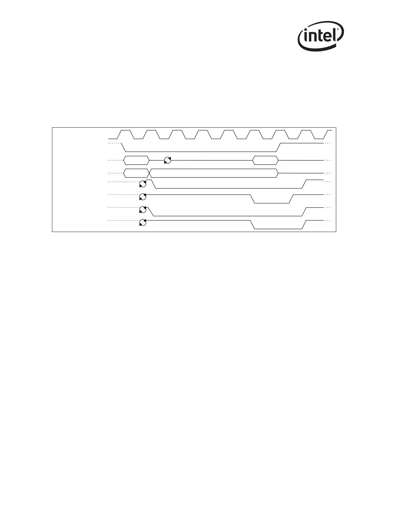
FLASH Memory Interface
7.2.1
Read Accesses
Upon reads to the FLASH address space, the Ethernet controller uses the TRDY# signal to insert
target wait states until valid data can be read from the FLASH device and presented on the data
lines. When TRDY# is asserted, the Ethernet controller drives valid data on the data lines. The
processor master can then complete normal data read cycle by asserting IRDY# when it is ready.
CLK
1
2
3
4
5
6
7
8
9
FRAME#
AD
ADDRESS
DATA
CBE#
MEM-RD
BE#s
IRDY#
TRDY#
DEVSEL#
STOP#
Figure 7-1. FLASH Buffer Read Cycles
7.2.2
Write Accesses
The processor, as the initiator, drives the address lines AD[63:0], the command and byte enable
lines [7:0]#, and the control lines IRDY# and FRAME#. It also provides the Ethernet controller
with valid data immediately after asserting TRDY#. The Ethernet controller controls the TRDY#
signal and deasserts it for a certain number of clocks until valid data is written to the FLASH
buffer. By asserting TRDY#, the Ethernet controller signals the processor that the current data
phase has completed.
128
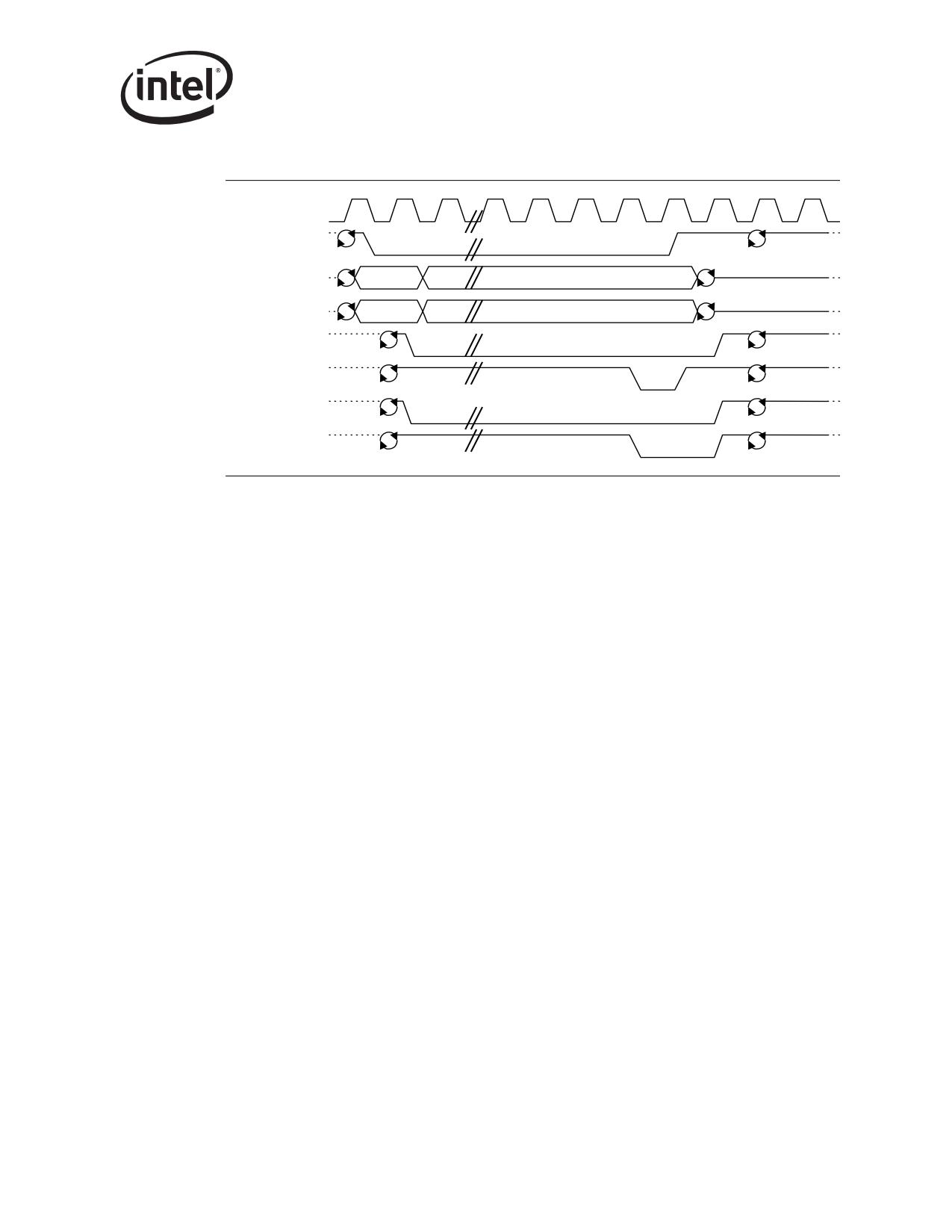
FLASH Memory Interface
CLK
1
2
3
7
8
9
10
11
12
13
14
FRAME#
AD
ADDRESS
DATA
MEM-WR
BE#s
CBE#
IRDY#
TRDY#
DEVSEL#
STOP#
Figure 7-2. FLASH Buffer Write Cycle
129
FLASH Memory Interface
Note: This page is intentionally left blank.
130
Power Management
6
6.1
Introduction to Power Management
The PCI/PCI-X Family of Gigabit Ethernet Controllers support the Advanced Configuration and
Power Interface (ACPI) specification as well as Advanced Power Management (APM). This
section describes how Power Management is implemented in the Ethernet controllers.
Note: The 82541ER does not support ACPI or APM wakeup.
Power Management can be disabled via bits in the Initialization Control Word 2 which is loaded
from the EEPROM during power-up reset. See the EEPROM description in Section 5.6.12 for
further details. Even when disabled, the Power Management register set is still present.
The Ethernet controller supports the following Power Management related features:
• Power states of D0 & D3hot with optional D3cold support
• Power(D3) < Power(D0)
• Wakeup
6.2
Assumptions
The following assumptions apply to the implementation of Power Management for the Ethernet
controller.
• Any time LAN_PWR_GOOD is asserted all power supplies are stable, RST# is stable, and the
clock is stable.
• Prior to transition from D0 to the D3 state, the operating system ensures that the software
device driver is disabled and all pending bus transactions are complete or cleanly terminated.
• The driver sets up the filters prior to the system transitioning the Ethernet controller to the D3
state.
• The system never deactivates the PCI clock in 66 MHz PCI mode or any PCI-X1 mode without
asserting RST#.
• No wakeup capability, except APM Wakeup if enabled in the EEPROM, is required after the
system asserts, then de-asserts RST#.
• No wakeup capability, except APM Wakeup if enabled in the EEPROM, is required after the
system puts the Ethernet controller in the D3 state and then returns it to D0.
• If the APMPME bit (bit 3) in the Wakeup Control Register (WUC.APMPME) is set to 1b, it is
permissible to assert PME# even when PME_En is 0b.
• The deassertion (rising) edge of RST# puts the Ethernet controller in the D0u state.
1.
The 82540EP/EM, 82541xx, and 82547GI/EI do not support PCI-X mode.
131
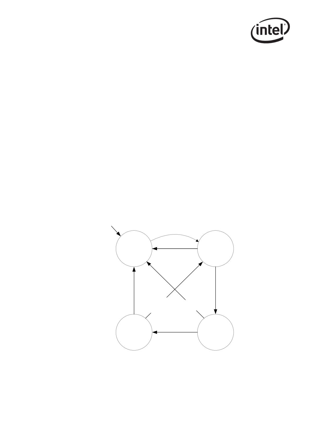
Power Management
6.3
D3cold support
If the AUX pin is connected to logic 1b, the Ethernet controller advertises D3cold Wakeup support.
The amount of power required for this function (which includes the entire Ethernet port circuitry)
is advertised in the Power Management Data Register which is loaded from the EEPROM.
If D3cold is supported, the PME_En and PME_Status bits of the Power Management Control/Status
Register (PMCSR), as well as their shadow bits in the Wakeup Control Register (WUC) are not
reset by RST#. If D3cold Wakeup is not supported, PMCSR and WUC is reset on the deassertion
(rising edge) of RST#.
The only effect of setting AUX to 1b is advertising D3cold Wakeup support and changing the reset
function of PME_En and PME_Status. The 82541PI/GI can enter a fully-disabled low-power state
in D3cold if an enable bit is set in the EEPROM. All remaining Ethernet controllers do nothing
different in D3cold compared to D3hot. AUX_POWER is level sensitive, and any changes are
immediately reflected in the D3cold Wakeup advertisements and the PME_En and PME_Status
reset function.
6.3.1
Power States
The Ethernet controller supports D0 and D3 power states defined in the PCI Power Management
Specification. D0 is divided into two sub-states: D0u, and D0a. In addition, it supports a Dr state
that is entered when RST# is asserted. Dr behaves the same as D3 except that the PCI bus is
isolated. Figure 6-1 illustrates the power states and the conditions that cause transitions from state
to state.
LAN_POWER_GOOD
assertion
RST#
deassertion
Dr*
D0u
RST# assertion
RST#
Enable Memory
assertion
Access
Write 00b
RST#
to Power
assertion
State
D3
D0a
Write 11b to
Power State
*equivalent to D3 except PCI pins are floated
Figure 6-1. Power State Transitions
132
Power Management
6.3.1.1
Dr State
At initial boot-up, once LAN_PWR_GOOD is asserted, the Ethernet controller reads the
EEPROM. If the APM Mode bit in the EEPROM’s Initialization Control Word 2 is set then APM
Wakeup is enabled.
The system may maintain RST# asserted for an arbitrary time. During this time, and for up to 1 ms
afterwards, the Ethernet controller does not assert any PCI signals except PME#.
During operation, the system may assert RST# at any time. In particular, if the system wishes an
Ethernet controller to enter the D3cold state it must assert RST# before dropping main power. Any
time RST# is asserted, the Ethernet controller transitions to the Dr state. It also floats all PCI
signals except PME# and remains in the “reset” state until no more than 1 ms after the deassertion
of RST#.
Internally, the Ethernet controller treats the reset state equivalently to D3. Any Wakeups enabled
before entering reset is maintained. For power savings, the Ethernet controller shuts down some
internal clocks and registers and deasserts PWR_STATE1. If Wakeup is not enabled, the Ethernet
controller also deasserts PWR_STATE0. As a result, the Ethernet controller won’t transmit any
frames in Dr state or send idles in TBI mode (82544GC/EI)/internal SerDes (82546GB/EB and
82545GM/EM)1.
The deassertion (rising edge) of RST# causes a transition to D0u.
6.3.1.2
D0u State
The D0u state is a low-power state used after RST# is deasserted, or when coming out of D3, but
before the Ethernet controller is initialized.
When entering D0u, the Ethernet controller disables Wakeups, resets the PHY, and then re-reads
the EEPROM. If the APM Mode bit in the EEPROM’s Initialization Control Word 2 is set, then
APM Wakeup is enabled.
Internally, D0u is treated like D3 and some internal clocks and registers are shut down. The D0u
state is exited when the system enables memory space access to the Ethernet controller by writing a
1b to the Memory Access Enable bit of the PCI Command Register.
Note:
In order for hardware to transition from D3 to the D0 state properly, BIOS should not alter the
Memory Access Enable or the I/O Access Enable bit of the PCI Command Register. Also, the PCI
configuration space must be programmed when hardware transitions out of D3 to D0.
1.
Not applicable to the 82541xx, 82547GI/EI, or 82540EP/EM.
133
Power Management
6.3.1.3
D0a (D0 active)
Once memory space is enabled, all internal clocks are activated, the Ethernet controller enters an
active state, and can then transmit and receive packets if properly configured by the software
driver. The controller also signals the PHY (if using the internal PHY) to indicate full speed/
power1. If APM Wakeup was activated it remains active. The software driver can deactivate APM
Wakeup by writing to the Wakeup Control Register (WUC), or activate other Wakeup Filters by
writing to the Wakeup Registers.
6.3.1.4
D3
Prior to transition from D0 to the D3 state, the software driver must ensure the Ethernet controller
transmit and receive functions have been disabled and all pending bus transactions are complete or
cleanly terminated. If Wakeup capability is needed, the software driver needs to set up the
appropriate Wakeup registers and the system needs to write a 1b to the PME_En bit of the Power
Management Control / Status Register (PMCSR) prior to the transition to D3.
When the system writes a 11b to the PowerState field of the Power Management Control/Status
Register (PMCSR) the Ethernet controller transitions to D3. Any Wakeups that are enabled remain
enabled. Upon transitioning to D3 the Ethernet controller clears the Memory Access Enable or the
I/O Access Enable bit of the PCI Command Register, which disables memory access decode. In
D3, the Ethernet controller only responds to PCI configuration accesses. It won’t generate master
cycles, transmit any frames on the TBI/internal SerDes2/internal PHY interface, or transmit idles in
TBI mode/internal SerDes if Wakeup is enabled.
For power savings the Ethernet controller shuts down some internal clocks and registers.
To transition back to D0u, the system writes a 00b to the Power State field of the Power
Management Control/Status Register (PMCSR).
6.3.2
Timing
The following sections give detailed timing for the state transitions. In the diagrams the dotted
connecting lines represent the Ethernet controller’s requirements, while the solid connecting lines
represent the Ethernet controller’s guarantees.
Note:
The following timing diagrams are not to scale. The clocks edges are shown to indicate running
clocks only and are not used to indicate the actual number of cycles for any operation.
If CLK_RUN# functionality is enabled in the EEPROM, then the 82541PI/GI/EI and 82540EP
Ethernet controllers assert the CLK_RUN# pin when it requires the PCI clock. Otherwise, the
clock is not required and the system might shut the PCI clock off.
1.
Not applicable to the 82541xx or 82547GI/EI.
2.
Not applicable to the 82541xx, 82547GI/EI, or 82540EP/EM.
134
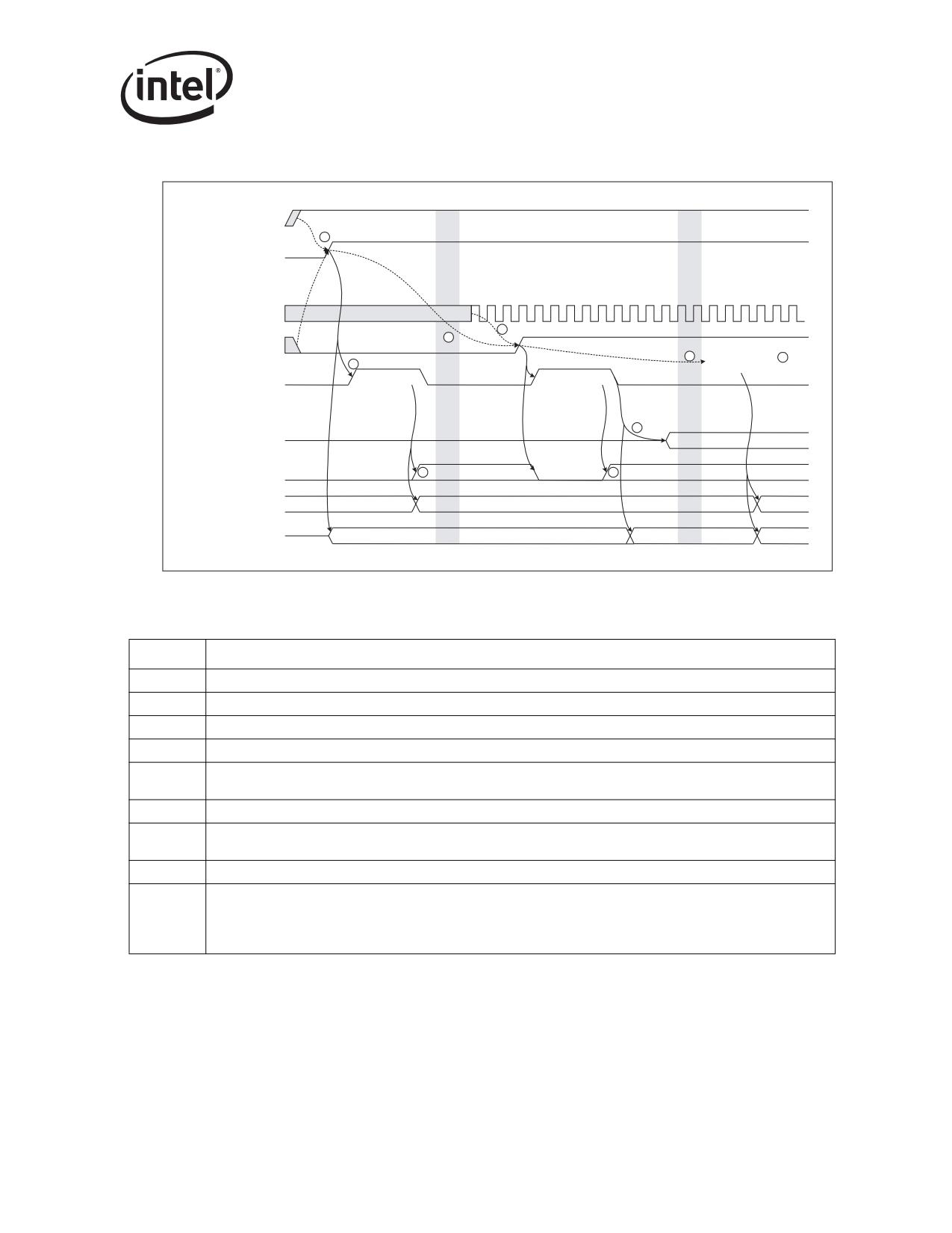
Power Management
6.3.2.1
Power Up (Off to Dr to D0u to D0a)
Power
1
LAN_POWER_GOOD
CLK#
5
4
RST#
8
Memory Access
9
2
Reading EEPROM
Read EEPROM
Read EEPROM
7
PCI Pins
Running
Wakeup Enabled
3
APM Wakeup
6
APM Wakeup
PWR_STATE[1:0]
00b
00b if wakeup is disabled, 10b if wakeup is enabled
11b
82544GC/EI Only
DState
Dr
D0u
D0a
Figure 6-2. Startup Timing
Diagram #
Notes
1
LAN_PWR_GOOD must not be asserted until all power supplies are good and the clock is stable.
2
An EEPROM read starts on the rising edge of LAN_PWR_GOOD and RST#.
3
APM Wakeup mode can be enabled based on what is read from the EEPROM.
4
The system can delay an arbitrary time before deasserting RST#.
The PCI 2.2 or 2.3 specification requires the clock to be active 100 µs before deasserting RST#. (Tclk-rst
5
parameter)
6
The deassertion edge of RST# causes the EEPROM to be re-read and Wakeup disabled.
Synchronizing the clock generators and circuit adjustments require up to 512 PCI clocks before the Ethernet
7
controller drives PCI signals and responds to PCI transactions.
8
The system can delay an arbitrary time before enabling Memory Access.
Writing a 1b to the Memory Access Enable or I/O Access Enable bit in the PCI Command Register transitions the
Ethernet controller from D0u to D0 state.
9
For the 82544GC/EI, writing a 1b to the Memory Access Enable or I/O Access Enable bit in the PCI Command
Register transitions the Ethernet controller from D0u to D0 state and asserts both PWR_STATE outputs.
135
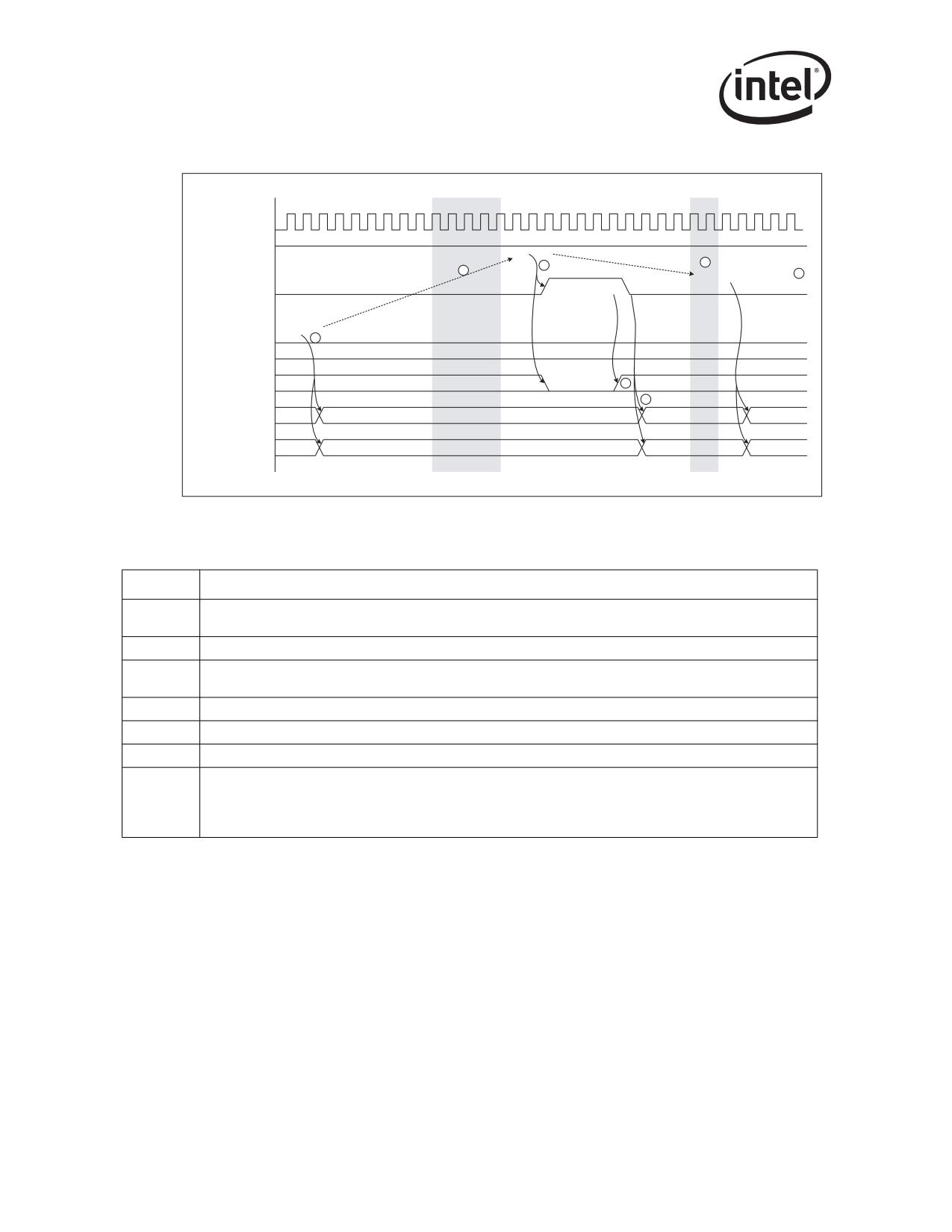
Power Management
6.3.2.2
Transition From D0a to D3 and Back Without PCI Reset
I_PCI_CLK
RST#
D0 Write
3
6
2
7
Memory Access Enable
Reading EEPROM
Read EEPROM
D3 write
1
PCI Pins
Run
ning
Wakeup Enabled
Any mode
4
APM only
5
PWR_STATE[1:0]
11b
00b if wakeup is disabled, 01b if wakeup is enabled
00b/01b
11b
82544GC/EI Only
DState
D0a
D3
D0u
D0
Figure 6-3. Transition from D0a to D3 and Back Without PCI Reset
Diagram #
Notes
Writing a 11b to the Power State field of the Power Management Control/Status Register (PMCSR) transitions
1
the Ethernet controller to D3.
2
The system can keep the Ethernet controller in D3 state for an arbitrary amount of time.
To exit D3 state the system writes 00b to the Power State field of the Power Management Control/Status
3
Register (PMCSR).
4
APM Wakeup mode can be enabled based on what is read in the EEPROM.
5
For the 82544GC/EI, PWR_STATE[1:0] is set to 01b if APM Wakeup is enabled, 00b otherwise.
6
The system can delay an arbitrary time before enabling memory access.
Writing a 1b to the Memory Access Enable or I/O Access Enable bit in the PCI Command Register transitions
the Ethernet controller from D0u to D0 state.
7
For the 82544GC/EI, writing a 1b to the Memory Access Enable or I/O Access Enable bit in the PCI Command
Register transitions the Ethernet controller from D0u to D0 state and asserts both PWR_STATE outputs.
136
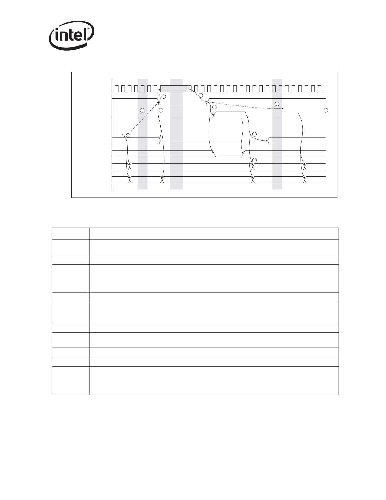
Power Management
6.3.2.3
Transition From D0a to D3 and Back with PCI Reset
CLK#
3
5
RST#
9
6
2
4
Memory Access Enable
10
Reading EEPROM
Read EEPROM
D3 write
1
7
PCI Pins
Running
Wakeup Enabled
Any mode
APM Wakeup
8
PWR_STATE[1:0]
11b
00b if w
akeup is disabled, 01b if wakeup is enabled
00b/01b
11b
82544GC/EI Only
DState
D0a
D3
Dr
D0u
D0a
Figure 6-4. Transition From D0a to D3 and Back with PCI Reset
Diagram #
Notes
Writing a 11b to the Power State field of the Power Management Control/Status Register (PMCSR) transitions
1
the Ethernet controller to D3.
2
The system can delay an arbitrary amount of time between setting D3 mode and asserting RST#.
In 66 MHz or PCI-Xa modes the system must assert RST# before stopping the PCI clock. It may assert RST#
without stopping the clock.
3
For the 82541PI/GI/EI and 82540EP, If CLK_RUN# is enabled, then they do not require a continuous clock
during this time, but does require that the system drive the clock in response to CLK_RUN# assertion.
4
Upon assertion of RST# the Ethernet controller floats all PCI pins except PME# and goes to “Dr” state.
In 66 MHz or PCI-X modes, the PCI 2.2 and 2.3 specification requires the system to start the PCI clock 100 µs
5
before deassertion of RST#. In 33 MHz systems the PCI clock can start and stop at any time independent of
RST#.
6
The deassertion edge of RST# causes the EEPROM to be re-read and Wakeup disabled.
Synchronizing the clock circuits and circuit adjustments require up to 512 PCI clocks before the Ethernet
7
controller drives PCI signals and responds to PCI transactions.
8
For the 82544GC/EI, O_PWR_STATE is set to 01b if APM Wakeup is enabled, 00b otherwise.
9
The system can delay an arbitrary time before enabling memory access.
Writing a 1b to the Memory Access Enable or I/O Access Enable bit in the PCI Command Register transitions
the Ethernet controller from D0u to D0 state.
10
For the 82544GC/EI, writing a 1b to the Memory Access Enable or I/O Access Enable bit in the PCI Command
Register transitions the Ethernet controller from D0u to D0 state and asserts both PWR_STATE outputs.
a.
Not applicable to the 82541xx, 82547GI/EI, or 82540EP/EM.
137
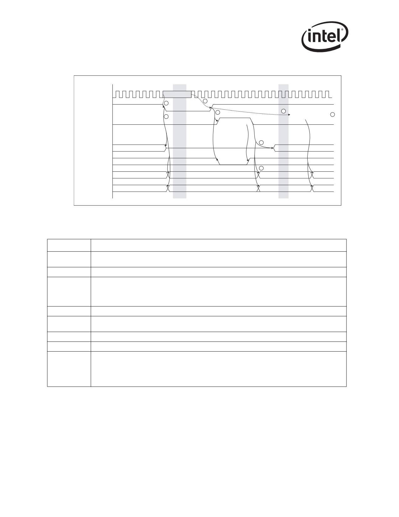
Power Management
6.3.2.4
PCI Reset Without Transition to D3
CLK#
3
1
RST#
4
7
Memory Access Enable
8
2
Reading EEPROM
Read EEPROM
5
PCI Pins
Running
Running
Wakeup Enabled
Any mode
APM Wakeup
6
PWR_STATE[1:0]
11b
00b if wakeup is disabled, 01b if wakeup is enabled
00b/01b
11b
82544GC/EI Only
DState
D0a
Dr
D0u
D0a
Figure 6-5. PCI Reset Sequence
Diagram #
Notes
In 66 MHz or PCI-Xa modes, the system must assert RST# before stopping the PCI clock. It may assert RST#
1
without stopping the clock.
2
Upon assertion of RST# the Ethernet controller floats all PCI pins except PME# and goes to “Dr” state.
In 66 MHz or PCI-X modes the system must assert RST# before stopping the PCI clock. It may assert RST#
without stopping the clock.
3
For the 82541PI/GI/EI and 82540EP, If CLK_RUN# is enabled, then they do not require a continuous clock
during this time, but does require that the system drive the clock in response to CLK_RUN# assertion.
4
The deassertion edge of RST# caused the EEPROM to be re-read and Wakeup disabled.
Synchronizing the clock circuits and circuit adjustments require up to 512 PCI clocks before the Ethernet
5
controller drives PCI signals and responds to PCI transactions.
6
For the 82544GC/EI, PWR_STATE[1:0] is set to 01b if APM Wakeup is enabled, 00b otherwise.
7
The system can delay an arbitrary time before enabling memory access.
Writing a 1b to the Memory Access Enable or I/O Access Enable bit in the PCI Command Register transitions
the Ethernet controller from D0u to D0 state.
8
For the 82544GC/EI, writing a 1b to the Memory Access Enable or I/O Access Enable bit in the PCI
Command Register transitions the Ethernet controller from D0u to D0 state and asserts both PWR_STATE
outputs.
a.
Not applicable to the 82541xx, 82547GI/EI, or 82540EP/EM.
138

Power Management
6.3.3
PCI Power Management Registers
Power Management registers are part of the capabilities linked list pointed to by the Capabilities
Pointer (Cap_Ptr) in the PCI configuration space. Refer to Section 4.1.
All fields are reset by LAN_PWR_GOOD. All of the fields except PME_En and PME_Status are
reset by the deassertion (rising edge) of RST#. If AUX_POWER = 0b, the PME_En and
PME_Status fields also reset by the deassertion (rising edge) of RST#.
The following table lists the organization of the PCI Power Management Register Block:
Byte Offset
Byte 3
Byte 2
Byte 1
Byte 0
Power Management Capabilities
DCh
Next Item Ptr
Capability ID
(PMC)
PMCSR_BSE
Power Management Control / Status
E0h
Data
Bridge Support
Register (PMCSR)
Extensions
The following sections describe the register definitions, whether they are required or optional for
compliance, and how they are implemented in the Ethernet controller. Complete details can be
found in the PCI Power Management Interface specification.
Note: The offset indicated is the byte-offset from the position indicated by Cap_Ptr in the Configuration
Space Header.
6.3.3.1
Capability ID
1 Byte Offset = 0 (RO)
Bits
Default
R/W
Description
Read
ID - The Ethernet controller returns a value of 01h for this field, indicating
07:00
01h
Only
the linked list item as being the PCI Power Management Registers.
6.3.3.2
Next Item Pointer
1 Byte Offset = 1 (RO)
Bits
Default
R/W
Description
Next Item Pointer - This field provides an offset into the function’s PCI
Read
07:00
E4h
Configuration Space pointing to the location of next item in the function’s
Only
capability list. Its value of E4h points to the PCI-Xa capability.
a.
Not applicable to the 82541xx, 82547GI/EI, or 82540EP/EM.
139

Power Management
6.3.3.3
Power Management Capabilities - (PMC)
2 Bytes Offset = 2 (RO)
Bits
Default
R/W
Description
PME_Support - This 5-bit field indicates the power states in which the
function may assert PME#a. A value of 0b for any bit indicates that the
function is not capable of asserting the PME# signal while in that power
state.
bit (11) (XXXX1)b - PME# can be asserted from D0
bit (12) (XXX1X)b - PME# can be asserted from D1
bit (13) (XX1XX)b - PME# can be asserted from D2
bit (14) (X1XXX)b - PME# can be asserted from D3hot
Read
15:11
See text
bit (15) (1XXXX)b - PME# can be asserted from D3cold
Only
If Power Management is not disabled in the EEPROM, the Ethernet
controller supports PME# generation from D0 and D3hot states. If Power
Management is not disabled and AUX_POWER = 1b, the Ethernet
controller also supports the D3cold state.
Condition
Value
00000b
Power Management disabled in EEPROM
AUX_POWER = 01001b Power Management enabled,
AUX_POWER = 11001b Power Management enabled,
D2_Support - If this bit is set to 1b, supports the D2 Power Management
State.
Read
10
0b
The Ethernet controller returns a value of 0b for this bit indicating that it
Only
does not support D2 and cannot handle the PCI clock stopping in PCI
66 MHz mode (or PCI-Xb mode) without RST# being asserted.
D1_Support - If this bit is set to 1b, supports the D1 Power Management
Read
09
0b
State. The Ethernet controller returns a value of 0b for this bit indicating
Only
that it does not support D1.
Read
AUX Current - Specifies the auxiliary power current required for PME#
08:06
000b
Only
generation from D3cold if the Data Register is not implemented.
DSI - The Device Specific Initialization bit indicates whether special
initialization of this function is required (beyond the standard PCI
Read
configuration header) before the generic class device driver is able to use
05
1b
Only
it. The Ethernet controller returns a value of 1b for this bit indicating that
it’s device driver must be executed following transition to the D0
uninitialized state.
Read
04
0b
Reserved
Only
Loaded
PME_Clock - When this bit is a 1b it indicates that the function relies on
Read
03
from
the presence of the PCI clock for PME# operation. The controller loads
Only
EEPROM
this bit from the EEPROM. Otherwise, it returns a 0b.
Read
Version - A value of 010b indicates that this function complies with the
02:00
010b
Only
Revision 1.1 of the PCI Power Management Interface Specification.
a.
Not applicable to the 82541ER.
b.
Not applicable to the 82541xx, 82547GI/EI, or 82540EP/EM.
140

Power Management
6.3.3.4
Power Management Control / Status Register - (PMCSR)
2 Bytes Offset = 4 (RO)
Bits
Default
R/W
Description
PME_Status - This bit is set when the function would normally assert the
PME# signal independent of the state of the PME_En bit. The Ethernet
controller returns a value of 1b for this bit if a Wakeup condition has been
Read/
detected.
0b (see
15
Write 1b
description)
Writing a 1b clears this bit and deasserts PME#a.
to clear
If the AUX_POWER input is 1b, the PME_Status field is only reset by
LAN_PWR_GOOD. If AUX_POWER is 0b, PME_Status is also reset on the
deassertion (rising edge) of RST#.
00b
Data_Scale - This 2- bit read-only field indicates the scaling factor to be
01b if
used when interpreting the value of the Data register. This field outputs 01b
Read
14:13
Manageability is
(to indicate units of 0.1 watt) when Manageability is enabled in the
Only
enabled
EEPROM and the Data_Select field is set to 0, 3, 4, or 7, and 00b
otherwise.
(see description)
Data_Select - This 4-bit field is used to select which data is to be reported
Read/
12:09
0000b
through the Data register and Data_Scale field. These bits are only writable
Write
when Power Management is enabled via EEPROM.
PME_En - If Power Management is not disabled in the EEPROM, writing a
1b to this register enables Wakeup and causes the Ethernet controller to
assert PME# when it receives a Wakeup event enabled in the Wakeup Filter
Control Register (WUFC).
Note: This bit cannot be set for the 82541ER.
0b on Power-On
Read/
If Power Management is disabled in the EEPROM, writing a 1b to this bit
08
reset
Write
has no affect, and does not set the bit to 1b.
If the AUX_POWER input is 1b, the PME_En field is only reset by
LAN_PWR_GOOD. If AUX_POWER is 0b, it is also reset on the
deassertion (rising edge) of RST#.
Note: If APM Wakeup is enabled, the PME# pin can be asserted even if
PME_En is 0b. See Section 6.4.1 for details.
Read
07:02
000000b
Reserved - The Ethernet controller returns a value of 000000b for this field.
Only
PowerState - This 2-bit field is used both to determine the current power
state of a function and to set the function into a new power state. The
definition of the field values is as follows:
00b - D0
01b - D1 (ignored if written with this value)
10b - D2 (ignored if written with this value)
Read/
01:00
00b
Write
11b - D3
If software attempts to write an unsupported state to this field, 00b or 10b, or
if Power Management is disabled in the EEPROM, then the Ethernet
controller completes the write operation normally on the bus, however the
data is discarded and no state change occurs.
These bits are cleared and the power state is returned to D0 after the trailing
edge of RST#.
a.
Not applicable to the 82541ER.
This register is used to control and monitor power management events in the Ethernet controller. If
auxiliary power is present, as indicated by AUX_POWER = 1b, a PCI reset does not clear
PME_En and PME_Status.
141
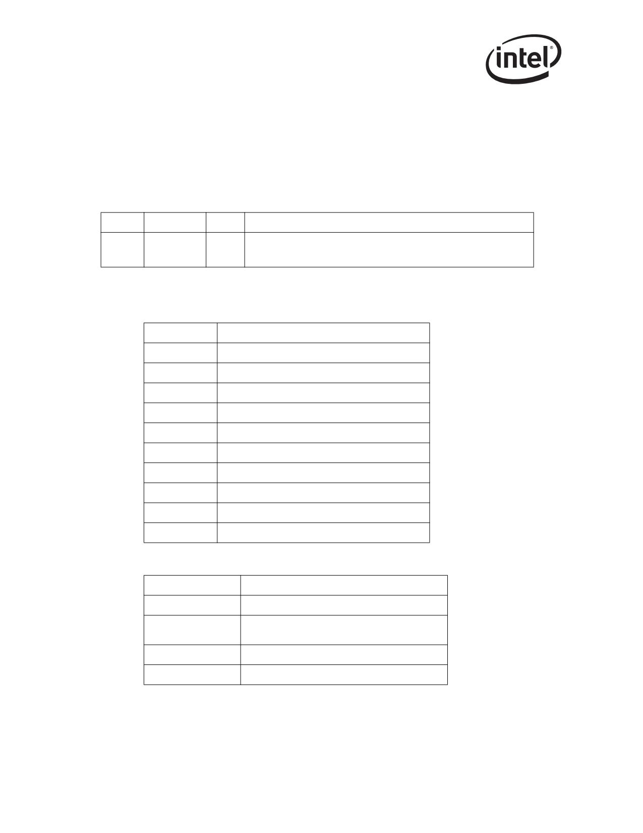
Power Management
6.3.3.5
PMCSR_BSE Bridge Support Extensions
1 Byte Offset = 6 (RO)
This register indicates support for PCI bridge specific functions. Note that these functions are not
implemented in the Ethernet controller and the values are set to 00h.
6.3.3.6
Data Register
1 Byte Offset = 7 (RO)
Bits
Default
R/W
Description
00h (loaded
Read
Data returned.
07:00
from
Only
See the following explanation.
EEPROM)
This register is used to report power consumption and heat dissipation. Its value and meaning is
determined by the value programmed in the Data_Select field of the Power Management Control/
Status Register (PMCSR).
Data Select
Meaning
0
D0 Power Consumed
1
D1 Power Consumed
2
D2 Power Consumed
3
D3 Power Consumed
4
D0 Power Dissipated
5
D1 Power Dissipated
6
D2 Power Dissipated
7
D3 Power Dissipated
8
Common power consumption of multi-function devices
9-15
Reserved
The units are defined by the Data_Scale field of the Power Management Control/Status Register.
Data Select
Meaning
0
Unknown (used for unsupported states)
0.1 Watts (used by Ethernet controller for supported
1
states)
2
0.01 Watts
3
0.001 Watts
If power management is disabled in the EEPROM, then the data register always reads 0b.
142
Power Management
If power management is not disabled and when the Data_Select field is programmed to 0 or 4, the
Ethernet controller sets the Data Register to the D0 Power value in the EEPROM. When the
Data_Select field is programmed to 3 or 7, the Ethernet controller sets the Data Register to the D3
Power value in the EEPROM. Otherwise it returns 0b.
6.4
Wakeup
The Ethernet controller supports two types of wakeup mechanisms:
• Advanced Power Management (APM) Wakeup
• ACPI Power Management Wakeup
Note: The 82541ER contains power management logic, but is not spec-compliant, because it does not
assert PME# for Magic Packets, Network Wakeup Packets, or link change status.
The ACPI Power Management Wakeup uses the PME# pin to wake up the system. The Advanced
Power Management Wakeup uses the PME# pin.
6.4.1
Advanced Power Management Wakeup
“Advanced Power Management Wakeup”, or “APM Wakeup”, was previously known as “Wake on
LAN”. The basic premise is to receive a broadcast or unicast packet with an explicit data pattern,
and then to assert a signal to wake up the system. In the earlier generations of the Ethernet
controller, this was accomplished by using special signal. The Ethernet controller would assert the
signal for approximately 50 ms to signal a wakeup. The 82544GC/EI uses the APM_WAKEUP
pin for this function. For the remaining Ethernet controllers, the PCI PME# signal has been used to
wake up the system.
On power-up, the Ethernet controller reads the APM Enable bits from the EEPROM Initialization
Control Word 2 into the APM Enable (APME) bits of the Wakeup Control Register (WUC). These
bits control enabling of APM Wakeup.
When APM Wakeup is enabled, the Ethernet controller checks all incoming packets for “Magic
Packets”. See Section 6.4.3.1.4 for a definition of “Magic Packets*”.
Once the Ethernet controller receives a matching magic packet, it:
• Sets the PME_Status bit in the Power Management Control / Status Register (PMCSR) and
asserts PME#. If the Assert PME On APM Wakeup (APMPME) bit is set in the Wakeup
Control Register (WUCR).
• Stores the first 128 bytes of the packet in the Wakeup Packet Memory (WUPM).
• Sets the Magic Packet Received bit in the Wakeup Status Register (WUS).
• Sets the packet length in the Wakeup Packet Length Register (WUPL).
• Asserts PME# until the driver clears the Magic Packet Received AMAG bit in the Wakeup
Status Register (WUS), the driver clears the Assert PME On APM Wakeup (APMPME) bit in
the Wakeup Control Register (WUC), or the driver disables APM Wakeup.
• For the 82544GC/EI only, asserts APM_WAKEUP for 50 ms. For purposes of
APM_WAKEUP assertion, the 82544GC/EI ignores any additional magic packets received
during that 50 ms. If the 82544GC/EI receives another magic packet afterwards, it reasserts
APM_WAKEUP for another 50 ms.
143
Power Management
• Maintains the first magic packet received in the Wakeup Packet Memory (WPM) until the
driver writes a 0b to the Magic Packet Received MAG bit in the Wakeup Status Register
(WUS).
“APM Wakeup” is supported in all power states and only disabled if a subsequent EEPROM read
results in the APM Wakeup bit being cleared or software explicitly writes a 0b to the APM Wakeup
(APM) bit of the WUC register.
6.4.2
ACPI Power Management Wakeup
The Ethernet controller supports ACPI Power Management based wakeups. It generates system
wakeup events from three sources:
• Reception of a “Magic Packet”.
• Reception of a Network Wakeup Packet.
• Detection of a link change of state.
Note: The 82541ER does not support ACPI wakeup events.
Activating ACPI Power Management Wakeup requires:
• The software driver to program the Wakeup Filter Control Register (WUFC). This indicates
the packets the driver wishes to wake up and supplies the necessary data to the IP Address
Table (IPAT) and the Flexible Filter Mask Table (FFMT), Flexible Filter Length Table (FFLT),
and the Flexible Filter Value Table (FFVT). The driver can also set the Link Status Change
Wakeup Enable (LNKC) bit in the Wakeup Filter Control Register (WUFC) to cause wakeup
when the link changes state.
• The OS to write a 1b to the Pme_En bit of the Power Management Control / Status Register
(PMCSR).
Normally, after enabling wakeup, the OS sets the Ethernet controller to D3 (low-power mode).
Once wakeup is enabled, the Ethernet controller monitors incoming packets, first filtering them
according to its standard address filtering method, then filtering them with all of the enabled
wakeup filters. If a packet passes both the standard address filtering and at least one of the enabled
wakeup filters, the Ethernet controller:
• Sets the PME_Status bit in the Power Management Control / Status Register (PMCSR)
• Assert PME#. If the PME_En bit in the Power Management Control / Status Register
(PMCSR) is set.
• Stores the first 128 bytes of the packet in the Wakeup Packet Memory.
• Sets one or more of the “Received” bits in the Wakeup Status Register (WUS). Note that the
Ethernet controller sets more than one bit if a packet matches more than one filter.
• Sets the packet length in the Wakeup Packet Length Register (WUPL).
If enabled, a link state change wakeup causes similar results. For example, setting PME_Status,
asserting PME#, and setting the Link Status Changed (LNKC) bit in the Wakeup Status Register
(WUSR) when the link goes up or down.
PME# remains asserted until the OS either writes a 1b to the PME_Status bit of the PMCSR
register or writes a 0b to the Pme_En bit.
144
Power Management
After receiving a wakeup packet, the Ethernet controller ignores any subsequent wakeup packets
until the driver clears all of the “Received” bits in the Wakeup Status Register (WUS). It also
ignores link change events until the driver clears the Link Status Changed (LNKC) bit in the
Wakeup Status Register (WUSR).
6.4.3
Wakeup Packets
The Ethernet controller supports various wakeup packets using two types of filters:
• Pre-defined Filters
• Flexible Filters
Each of these filters are enabled if the corresponding bit in the Wakeup Filter Control Register
(WUFC) is set to 1b.
6.4.3.1
Pre-Defined Filters
The following packets are supported by the Ethernet controller’s pre-defined filters:
• Directed Packet (including exact, multicast indexed, and broadcast)
• Magic Packet* (not applicable to the 82541ER)
• ARP/IPv4 Request Packet (ARP Request Packet for the 82544GC/EI)
• Directed IPv4 Packet (Directed IP Packet for the 82544GC/EI)
• Directed IPv6 Packet1
Each of these filters are enabled if the corresponding bit in the Wakeup Filter Control Register
(WUFC) is set to 1b.
The following explanation of each filter includes a table listing which bytes at which offsets are
compared to determine if the packet passes the filter. Note that both VLAN2 frames and LLC/Snap
can increase the given offsets if they are present (see Section 9.3 for details).
For the 82541PI/GI/EI and 82547GI/EI, various tables can also include a reference to a possible
VLAN Tag and LLC/SNAP Header. These Ethernet controllers detect VLAN and LLC/Snap
frames by checking the initial size/type field. They first check for a VLAN header by comparing
the size/type field to the value programmed in the VLAN EtherType register. If the field matches,
the Ethernet controllers consider the frame a VLAN frame. They then check the VLAN ID against
the values programmed in the VLAN Filter Table Array. If the ID matches the packet, processing
continues. If the ID doesn’t match, or the CTRL.VME bit is 0b, and the VLAN Tag is listed as
compare in the table, the packet is not considered a wakeup packet.
After processing a possible VLAN Tag, the 82541PI/GI/EI and 82547GI/EI Ethernet controllers
check for an LLC/SNAP Header. If the size/type field is less than or equal to 1500 bytes, they
check the following 6 bytes for the pattern of AAAA03000000h. If the pattern matches, then the
packet processing continues. If the pattern doesn’t match, and the LLC/SNAP Header is listed as
compare or check in the table, the packet is not considered a wakeup packet.
6.4.3.1.1
Directed Exact Packet
1.
Not applicable to the 82544GC/EI.
2.
Not applicable to the 82541ER.
145

Power Management
The Ethernet controller generates a wakeup event after receiving any packet whose destination
address matches one of the 16 valid programmed Receive Addresses if the Directed Exact Wakeup
Enable bit is set in the Wakeup Filter Control Register (WUFC.EX).
# of
Offset
Field
Value
Action
Comment
bytes
Match any pre-
0
6
Destination Address
Compare
programmed address
6.4.3.1.2
Directed Multicast Packet
For multicast packets, the upper bits of the incoming packet’s destination address indexes a bit
vector (Multicast Table Array) that indicates whether to accept the packet. If the Directed Multicast
Wakeup Enable bit set in the Wakeup Filter Control Register (WUFC.MC) and the indexed bit in
the vector is one then the Ethernet controller generates a wakeup event. The exact bits used in the
comparison are programmed by software in the Multicast Offset field of the Receive Control
Register (RCTL.MO).
# of
Offset
Field
Value
Action
Comment
Bytes
0
6
Destination Address
Compare
See Section 6.4.3.1.2.
6.4.3.1.3
Broadcast
If the Broadcast Wakeup Enable bit in the Wakeup Filter Control Register (WUFC.BC) is set, the
Ethernet controller generates a wakeup event when it receives a broadcast packet.
# of
Offset
Field
Value
Action
Comment
bytes
0
6
Destination Address
FF*6
Compare
6.4.3.1.4
Magic Packet*1
Magic Packet* technology is defined at: http://www.amd.com/products/npd/overview/20212.html.
The Ethernet controller expects the destination address to:
1. Be the broadcast address (FF.FF.FF.FF.FF.FF)
2. Match the value in Receive Address Register 0 (RAH0, RAL0). This is initially loaded from
the EEPROM but can be changed by the software driver.
3. Match any other address filtering enabled by the software driver.
The Ethernet controller searches for the contents of Receive Address Register 0 (RAH0, RAL0) as
the embedded IEEE address. It considers any non FF byte after a series of at least 6 FFs to be the
start of the address for comparison purposes (for example, it catches the case of 7 FFs followed by
the address). As soon as one of the first 96 bytes after a string of FFs doesn’t match, it continues to
search for anther set of at least 6 FFs followed by the 16 copies of the IEEE address later in the
packet. Note that this definition precludes the first byte of the destination address from being FF.
1.
Not applicable to the 82541ER.
146
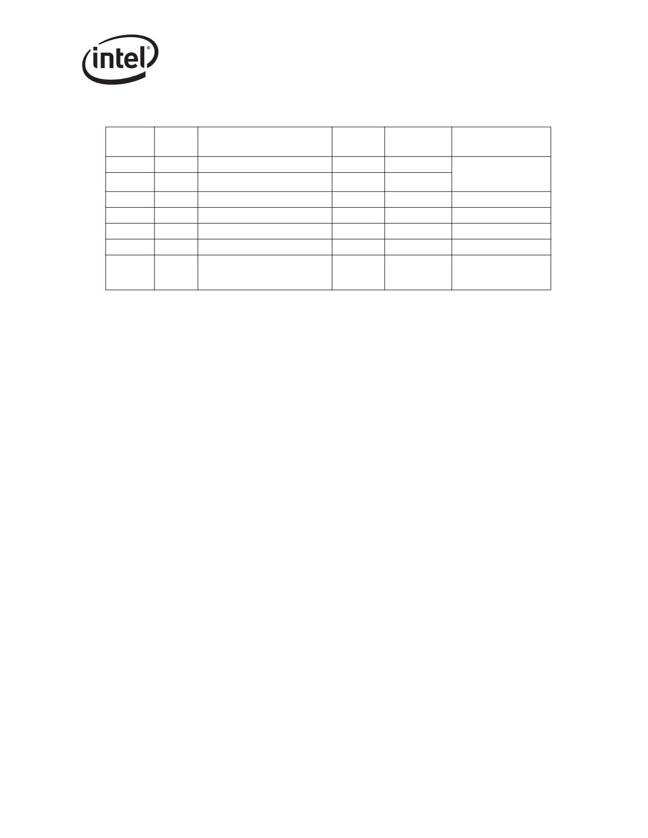
Power Management
# of
Offset
Field
Value
Action
Comment
bytes
0
6
Destination Address
Compare
MAC Header -
processed by main
6
6
Source Address
Skip
address filter
12a
8
Possible LLC/SNAP Header
Skip
12a
4
Possible VLAN Tag
Skip
12a
4
Type
Skip
any
6
Synchronizing Stream
FF*6+
Compare
Compared to Receive
any+6
96
16 copies of Node Address
A*16
Compare
Address Register 0
(RAH0, RAL0)
a.
Not applicable to the 82541PI/GI/EI and 82547GI/EI.
A Magic Packet’s destination address must match the address filtering enabled in the configuration
registers with the exception that broadcast packets are considered to match even if the Broadcast
Accept bit of the Receive Control Register (RCTL.BAM) is 0b. If APM Wakeup is enabled in the
EEPROM, Ethernet controller starts up with the Receive Address Register 0 (RAH0, RAL0)
loaded from the EEPROM. This is enables it to accept packets with the matching IEEE address
before the driver comes up.
Note: Accepting broadcast magic packets for wakeup purposes when the Broadcast Accept bit of the
Receive Control Register (RCTL.BAM) is 0b is a change from the 82544GC/EI Ethernet
controller, which initialized RCTL.BAM to 1b if APM was enabled in the EEPROM, but then
required that bit to be 1b to accept broadcast Magic Packets, unless broadcast packets passed
another perfect or multicast filter.
147