FANUC I/O Unit–MODEL A CONNECTION AND MAINTENANCE MANUAL MARMGIOMA12801E REV. F (B-61813EN/06) - page 4
5.DIGITAL INPUT/OUTPUT
B-61813E/06
CONNECTION
MODULES
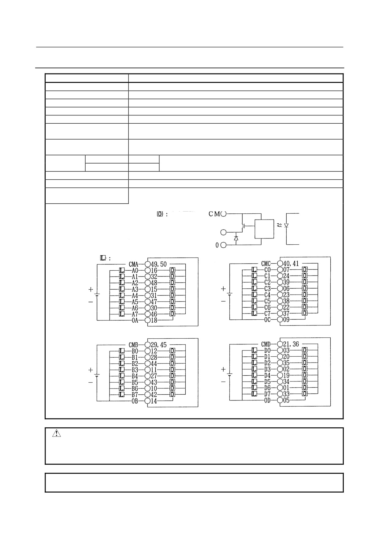
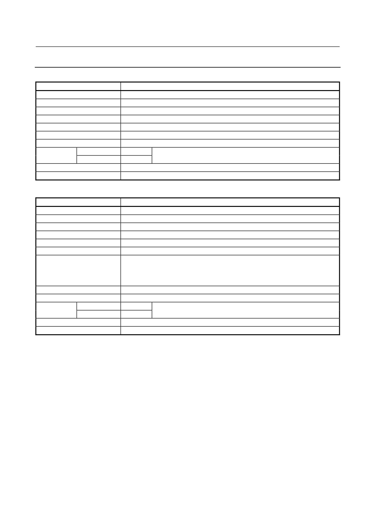
5.3.27 AOD32D1 - Output Module
Item
Specifications
Points/module
32 points
Points/common
8 points/common
Sink/source current
Source current type
Rated load voltage
12 to 24VDC +20%, −15%
Maximum load current
0.3A (however 2A/common)
Maximum voltage drop when
0.24V (load current ×0.8Ω)
ON
Maximum leak current when
0.1mA
OFF
Response time
OFF→ON
Max.2ms
This is the value from input to output in the module. The actual value is
ON→OFF
Max.2ms
determined by adding it to the scanning time depending on each system.
Output display
Not provided
External connection
Connector (HONDA TSUSHIN MR-50RMA) (male)
Terminal connection and
circuitry
Output circuit
Internal
circuit
Load
CAUTION
Be sure to wire pins 5, 9, 14, and 18 as shown above. Keeping the pin open
prevents this module from operating normally, possibly leading to a serious
accident.
NOTE
For the common (CMA, CMB, CMC, CMD), make sure to use both of them.
- 65 -
5. DIGITAL INPUT/OUTPUT
MODULES
CONNECTION
B-61813E/06
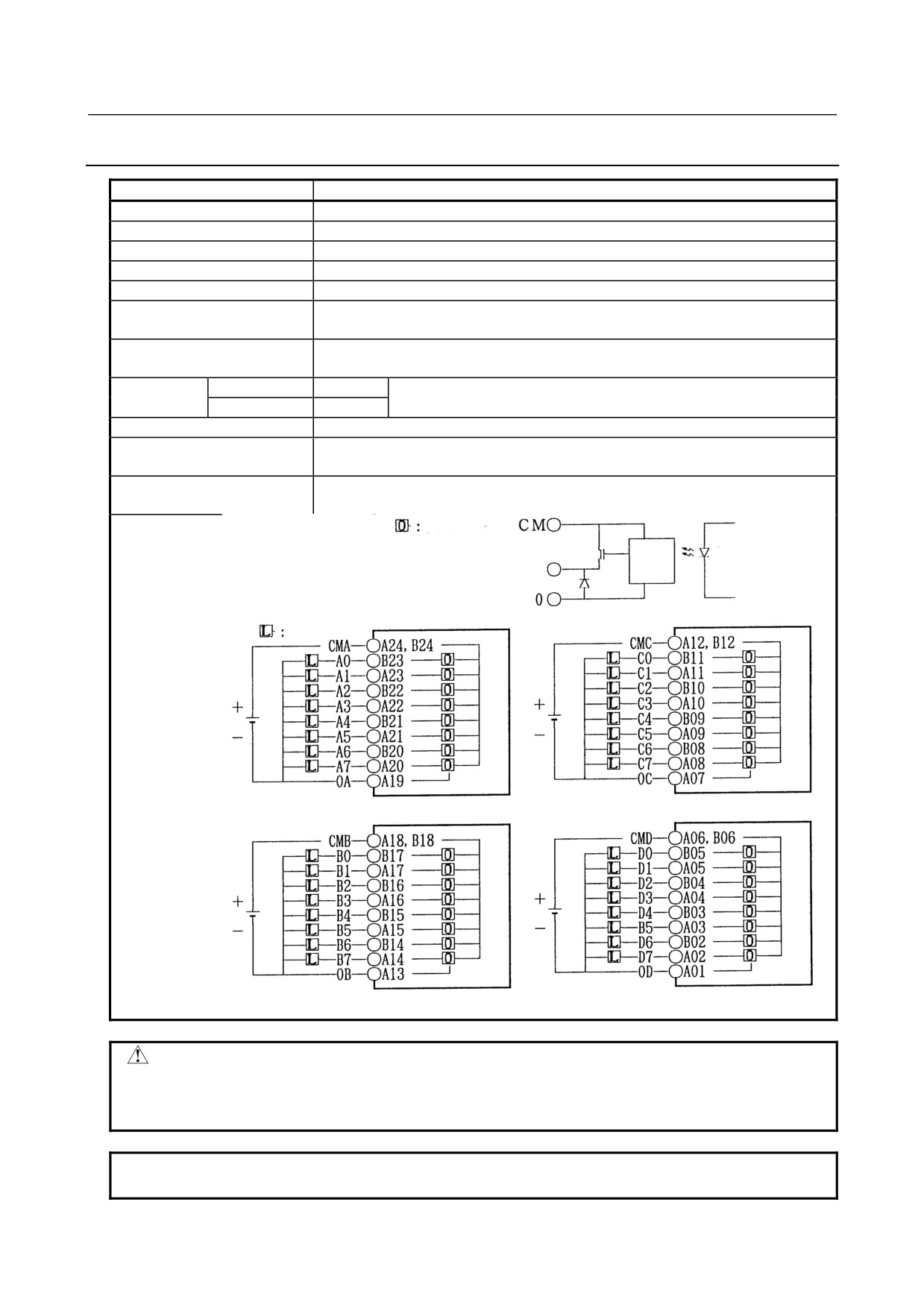
5.3.28 AOD32D2 - Output Module
Item
Specifications
Points/module
32 points
Points/common
8 points/common
Sink/source current
Source current type
Rated load voltage
12 to 24VDC +20%, −15%
Maximum load current
0.3A (however 2A/common)
Maximum voltage drop when
0.24V (load current ×0.8Ω)
ON
Maximum leak current when
0.1mA
OFF
Response time
OFF→ON
Max.2ms
This is the value from input to output in the module. The actual value is
ON→OFF
Max.2ms
determined by adding it to the scanning time depending on each system.
Output display
Not provided
External connection
Connector (HIROSE ELECTRIC HIF3BB-50PA-2.54DS in accordance with MIL
standard)
Terminal connection and
circuitry
Output circuit
Internal
circuit
Load
CAUTION
Be sure to wire pins A01, A07, A13, and A19 as shown above. Keeping the pin
open prevents this module from operating normally, possibly leading to a serious
accident.
NOTE
For the common (CMA, CMB, CMC, CMD), make sure to use both of them.
- 66 -
5.DIGITAL INPUT/OUTPUT
B-61813E/06
CONNECTION
MODULES
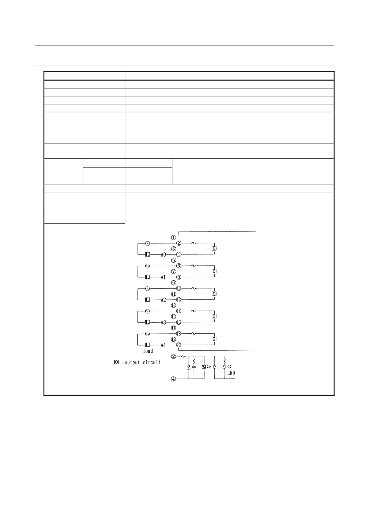
5.3.29 AOA05E - Output Module
Item
Specifications
Points/module
5 points
Points/common
1 points/common
Rated load voltage
100 to 230VAC ±15%, 47 to 63Hz
Maximum load current
2A/point (however 5A/module)
Maximum rush current
25A ( 1 period)
Limit of load
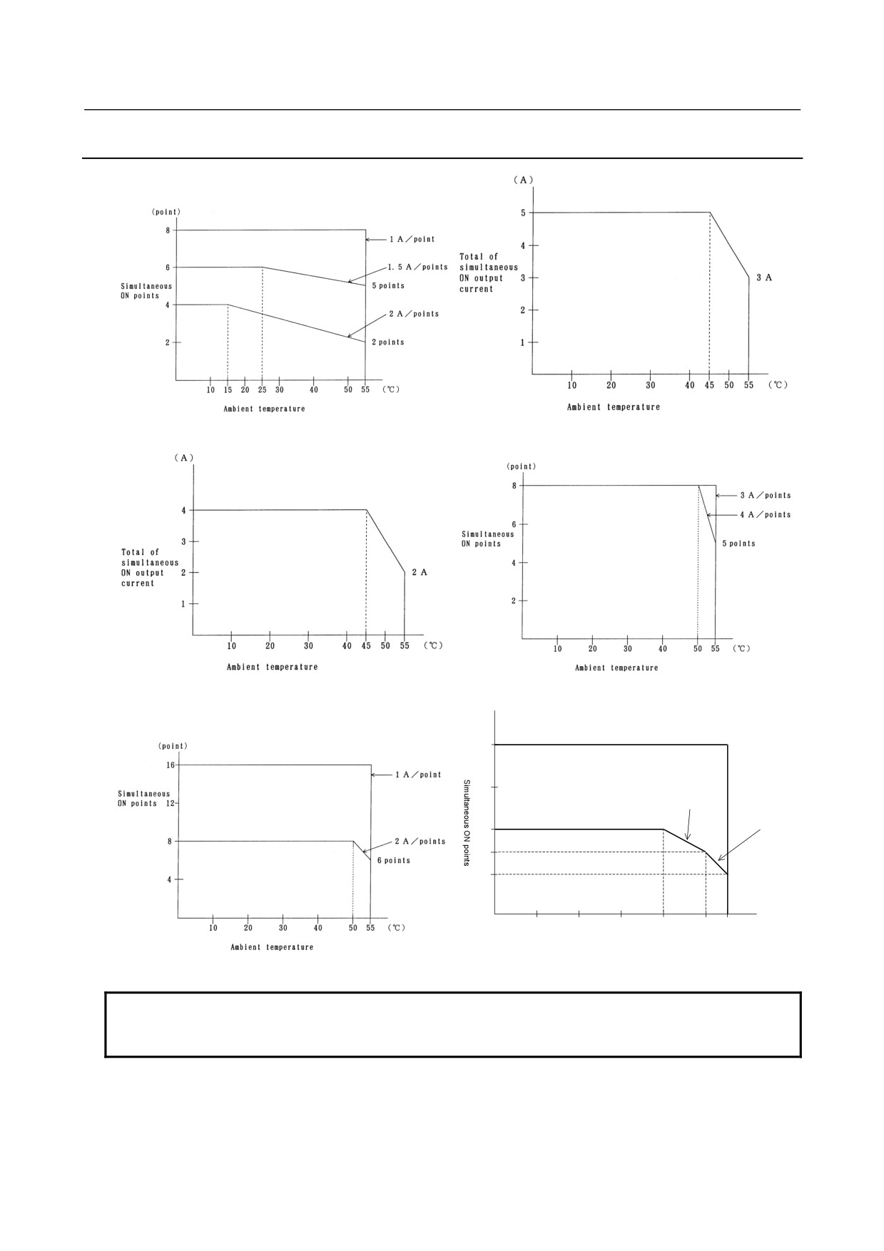
Refer to load reduction curve (Fig. 5.3 (b))
Maximum voltage drop when
1.5Vrms
ON
Maximum leak current when
3.0mA (115VAC), 6.0mA (230VAC)
OFF
Response time
OFF→ON
Max.1ms
This is the value from input to output in the module. The actual
ON→OFF
Half of the load
value is determined by adding it to the scanning time depending
frequency or less
on each system.
Output display
LED display
External connection
Terminal block connector (20 terminals, M3.5 screw terminal)
Fuse
3.2A, 1 piece for each output A0 to A4
Terminal connection and
circuitry
- 67 -
5. DIGITAL INPUT/OUTPUT
MODULES
CONNECTION
B-61813E/06
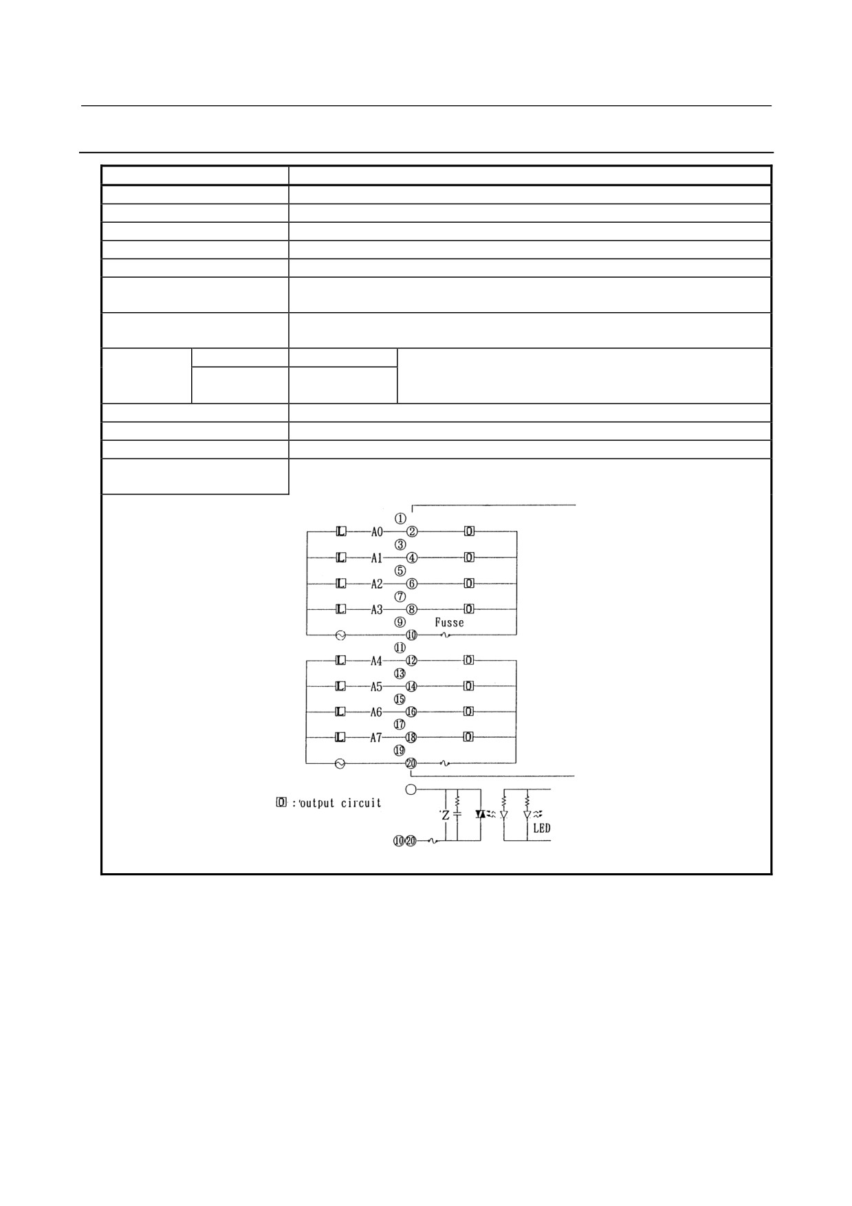
5.3.30 AOA08E - Output Module
Item
Specifications
Points/module
8 points
Points/common
4 points/common
Rated load voltage
100 to 230VAC ±15%, 47 to 63Hz
Maximum load current
1A/point (however 2A/common)
Maximum in rush current
10A (1 period)
Maximum voltage drop when
1.5Vrms
ON
Maximum leak current when
3.0mA (115VAC), 6.0mA (230VAC)
OFF
Response time
OFF→ON
Max.1ms
This is the value from input to output in the module. The actual
ON→OFF
Half of the load
value is determined by adding it to the scanning time depending
frequency or less
on each system.
Output display
LED display
External connection
Terminal block connector (20 terminals, M3.5 screw terminal)
Fuse
3.2A, 1 piece for each output A0 to A3 and A4 to A7
Terminal connection and
circuitry
Load
- 68 -
5.DIGITAL INPUT/OUTPUT
B-61813E/06
CONNECTION
MODULES
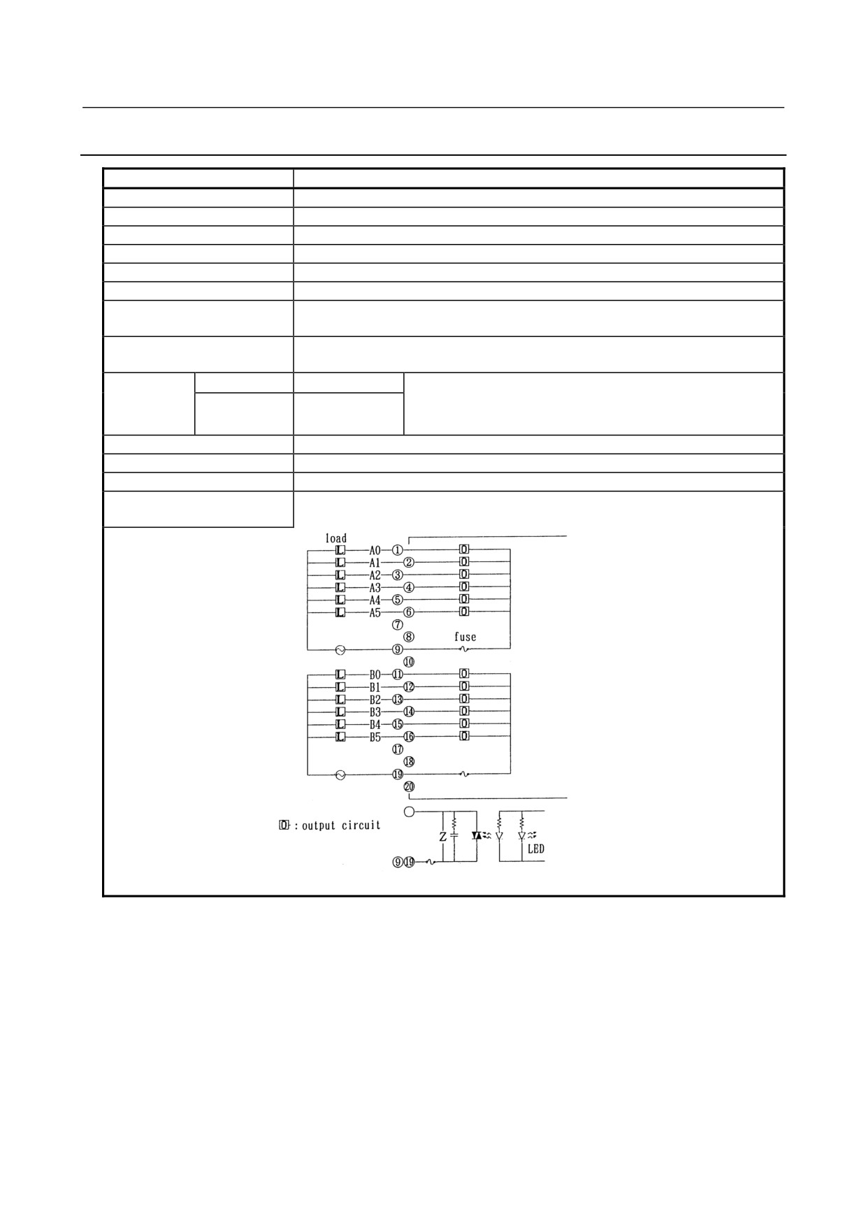
5.3.31 AOA12F - Output Module
Item
Specifications
Points/module
12 points
Points/common
6 points/common
Rated load voltage
100 to 115VAC ±15%, 47 to 63Hz
Maximum load current
0.5A/point (however, 2A/common)
Maximum in rush current
5A (1 period)
Limit of load
Refer to load reduction curve (Fig. 5.3 (c))
Maximum voltage drop when
1.5Vrms
ON
Maximum leak current when
1.5mA (115VAC)
OFF
Response time
OFF→ON
Max.1ms
This is the value from input to output in the module. The actual
ON→OFF
Half of the load
value is determined by adding it to the scanning time depending
frequency or less
on each system.
Output display
LED display
External connection
Terminal block connector (20 terminals, M3.5 screw terminal)
Fuse
3.2A, 1 piece for each output A0 to A5 and B0 to B5
Terminal connection and
circuitry
- 69 -
5. DIGITAL INPUT/OUTPUT
MODULES
CONNECTION
B-61813E/06
5.3.32 AOR08G - Output Module
Item
Specifications
Points/module
8 points
Points/common
1 points/common
Maximum load
30VDC/250VAC, 4A (resistance load)
Minimum load
5VDC, 10mA
Limit of load
Refer to load reduction curve (Fig. 5.3 (d))
Response time
OFF→ON
Max.15ms
This is the value from input to output in the module. The actual value is
ON→OFF
Max.15ms
determined by adding it to the scanning time depending on each
system.
Output display
LED display
External connection
Terminal block connector (20 terminals, M3.5 screw terminal)
Relay life
Mechanical
Min. 20,000,000 times
Electrical
Min. 100,000 times (resistance load)
Terminal connection and
circuitry
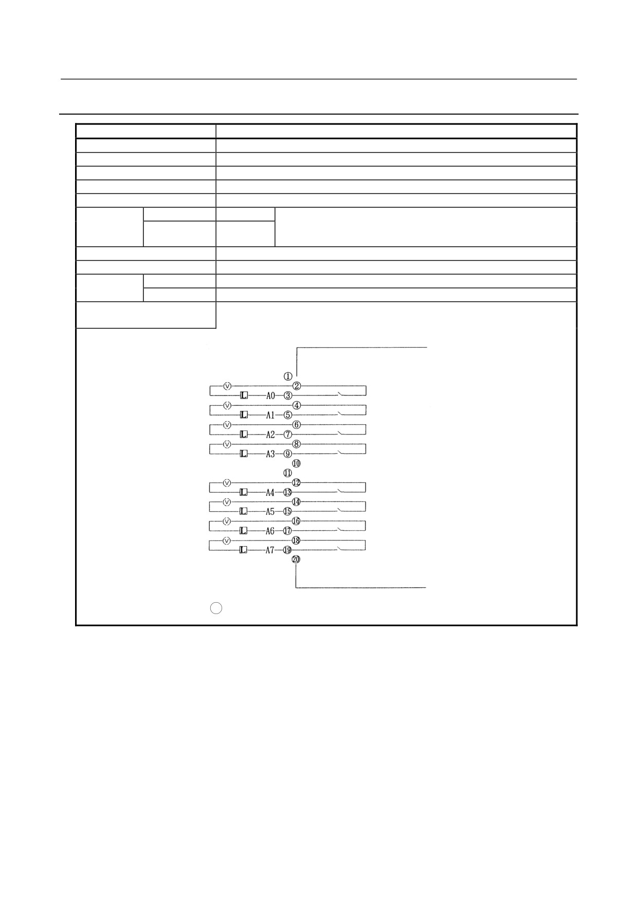
V : Direct current power or alternating current power
- 70 -
5.DIGITAL INPUT/OUTPUT
B-61813E/06
CONNECTION
MODULES
5.3.33 AOR16G - Output Module
Item
Specifications
Points/module
16 points
Points/common
4 points/common
Maximum load
30VDC/250VAC, 2A (resistance load)
Minimum load
5VDC, 10mA
Maximum current
4A/common
Limit of load
Refer to load reduction curve (Fig. 5.3 (e))
Response time
OFF→ON
Max.15ms
This is the value from input to output in the module. The actual value is
ON→OFF
Max.15ms
determined by adding it to the scanning time depending on each system.
Output display
LED display
External connection
Terminal block connector (20 terminals, M3.5 screw terminal)
Relay life
Mechanical
Min. 20,000,000 times
Electrical
Min. 100,000 times (resistance load)
Terminal connection and
circuitry
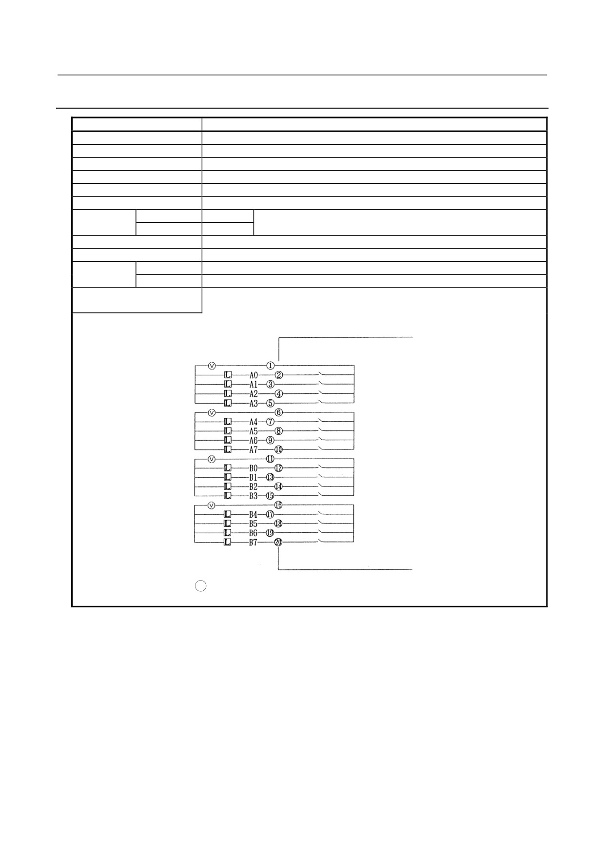
Load
V : Direct current power or alternating current power
- 71 -
5. DIGITAL INPUT/OUTPUT
MODULES
CONNECTION
B-61813E/06
5.3.34 AOR16H2 - Output Module
Item
Specifications
Points/module
16 points
Points/common
4 points/common
Maximum load
30VDC, 2A (resistance load)
Minimum load
5VDC, 10mA
Maximum current
4A/common
Limit of load
Refer to load reduction curve (Fig. 5.3 (e))
Response time
OFF→ON
Max.15ms
This is the value from input to output in the module. The actual value is
ON→OFF
Max.15ms
determined by adding it to the scanning time depending on each system.
Output display
LED display
External connection
Connector (HIROSE ELECTRIC HIF3BB-50PA-2.54DS in accordance with MIL
standard)
Relay life
Mechanical
Min. 20,000,000 times
Electrical
Min. 100,000 times (resistance load)
Terminal connection and
circuitry
- 72 -
5.DIGITAL INPUT/OUTPUT
B-61813E/06
CONNECTION
MODULES
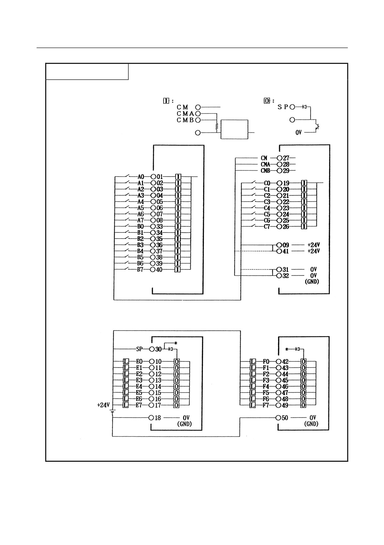
5.3.35 AIO40A - Input/output Module
-
Input specifications
Item
Specifications
Points/module
24 points
Points/common
24 points/common
Sink/source current
Both directions
Input voltage
24VDC +10%, −20%
Input current
7.5mA (average)
ON voltage, current
Min. 18VDC, min. 6mA
OFF voltage, current
Max. 6VDC, max. 1.5mA
Response time
OFF→ON
Max.20ms
This is the value from input to output in the module. The actual value is
ON→OFF
Max.20ms
determined by adding it to the scanning time depending on each system.
Input display
Not provided
External connection
Connector (HONDA TSUSHIN MR-50RMA, shared by output signals) (male)
-
Output specifications
Item
Specifications
Points/module
16 points
Points/common
16 points/common
Sink/source current
Sink current type
Rated load voltage
24VDC +20%, −15%
Maximum load current
0.2A (however 2A/common)
Maximum in rush current
0.2A
Limit of load
• If the output current per point is 0.1 A or lower, all of the 16 points E0 to E7 and F0 to
F7 can be turned on at a time.
• If the output current per point is higher than 0.1 A but not higher than 0.2 A, do not
turn on more than 3 points at a time.
Maximum voltage drop when ON
1.5V
Maximum leak current when OFF
1.0mA (30VDC)
Response time
OFF→ON
Max.1ms
This is the value from input to output in the module. The actual value is
ON→OFF
Max.1ms
determined by adding it to the scanning time depending on each system.
Output display
Not provided
External connection
Connector (HONDA TSUSHIN MR-50RMA, shared by input signals) (male)
- 73 -
5. DIGITAL INPUT/OUTPUT
MODULES
CONNECTION
B-61813E/06
•Input/output module
Terminal connection and
circuitry
To the automatic
Input circuit
polarity
Output circuit
discrimination
circuit
Input section
Internal
circuit
Either 24 V or 0 V can be selected as an input common potential as shown above.
(Solid line: 24-V common. Dotted line: 0-V common.)
Output section
- 74 -
5.DIGITAL INPUT/OUTPUT
B-61813E/06
CONNECTION
MODULES
5.4
CAUTIONS REGARDING EACH INPUT/OUTPUT MODULE
5.4.1
Cautions Regarding Input Modules
1
Quick response type input modules have a low input filter time constant. So, contact chattering may
cause these input modules to read incorrect inputs. Restrict their use to connection with no-contact
devices and pay attention to noise sufficiently.
2
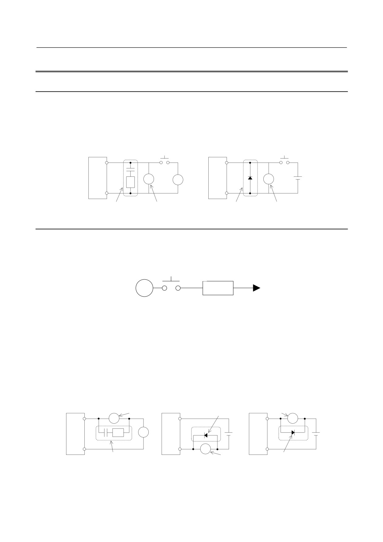
If an input contact is connected to an input module and inductive load in parallel, a surge voltage that
occurs across the load when the contact becomes off may cause the input module to malfunction. If
this is the case, attach a surge arrester to the load in parallel to suppress the surge voltage.
AC input
DC input
module
module
L
L
~
Surge arrester (like snubber circuit)
Inductive load
Diode
Inductive load
5.4.2
Cautions Regarding Output Modules
1
Even if the sequence program has turned off an output module, its internal stray capacity may cause an
output current to flow instantaneously through it when a voltage is applied abruptly to the load. In
order to evade this symptom, use the configuration that the load power is turned on/off on the primary
side, as shown below.
Primary side
Secondary side
Load power
~
2
Be sure to connect the power supply and common pins. Otherwise, current flow may get in the output
circuit, resulting in the output being turned on.
3
Measures for inductive loads
•
Do not turn on/off the output module repeatedly within a short period of time. The maximum
permissible ON/OFF frequency is: ON for at least 1 second and OFF for at least 1 second.
•
If the output load is inductive, connect a protection circuit like a surge killer or diode to the load
in parallel. Note, however, that, connection of a protection circuit may cause a delay in recovery
time. If this is a problem, use a CR snubber circuit instead of a surge killer or diode.
•
If the output module is used to control an inductive load like a lamp load, it is likely that output
turn-on rush current may damage the output element. Do not even instantaneously fail to observe
the current and voltage ratings.
Inductive load
Inductive load
Diode
AC output
DC output
DC output
module
L
module
module
L
Source type
Sink type
~
L
Surge arrester (like snubber circuit)
Inductive load
Diode
4
The number of output points that can be turned on at the same time varies depending on the output
voltage and ambient temperature. Getting out of the specification range may cause a module failure or
smoke. See the load reduction curve charts (Subsection 5.4.4) for each output module.
- 75 -
5. DIGITAL INPUT/OUTPUT
MODULES
CONNECTION
B-61813E/06
5.4.3
Cautions Regarding Relay Modules
1
Relays have a limited service life because their contacts are worn away. The service life of relays
varies depending on the environment in which they are used. Pay attention to the environment and
avoid exceeding the service life. If it is anticipated that the service life of a relay in a module will
expire, replace the module. If the service life of a relay expires, the module output becomes abnormal
because of a poor connection, leading to a possible machine breakdown and accident.
2
If a high open/close frequency is involved, use a DC or AC output module.
3
Cause the contacts of each relay to open at least once a year.
4
Provide a contact protection circuit for each relay in order to extend their contact life, suppress noise,
and prevent chars or nitric acid from developing due to arcs. An incorrect contact protection circuit
leads to an adverse result and causes contacts to be welded readily.
5
When connecting a capacitive load on the machine side, be sure to connect a current limiting resistor to
the capacitive load in series to observe the current and voltage ratings always
(not even
instantaneously fail).
6
Providing a contact protection circuit may cause a delay in a recovery time.
7
Even if a rush current lasts for a relatively long time, avoid shutting off a relay when the rush current is
flowing. Otherwise, its contacts may be welded.
8
When a lamp having a high amperage, in particular, is turned on or off, it is recommended to
previously perform a confirmation test on a real load.
9
When using a relay output to control an inductive or capacitive load, for example, directly to light a
lamp, provide a protective resistor between the output terminals in order to observe the current and
voltage ratings always (not even instantaneously fail). Otherwise, a rush current may damage the
relay.
10
The relay output module incorporates no fuse. In order to prevent burnout, it is recommended to use a
fuse rated twice the output rating at every external terminal.
11
Transfer phenomenon of relay contacts
•
An arc that occurs when a contact is opened and closed causes the materials of the contact poles
to melt, resulting in the molten material of one pole transferred to the other pole. As the number
of times that the contact is opened and closed increases, concave and convex portions develop on
the poles and eventually lock with one another, causing the contact to behave as if contact
welding had occurred.
•
Transfer phenomenon of relay contacts can occur even if the relay is used within the contact
rating. Check for a surge voltage and rush current. Consider using, for example, a surge killer or
current limiting resistor to suppress any surge voltage or rush current.
12
Using the relay module in an atmosphere containing silicon gas, sulfidizing gas, or organic gas may
cause contact surfaces to corrode or be covered with film that develops on them, leading to a poor
connection. Do not use the relay module in such an atmosphere. Take an effective measure for such an
atmosphere, for example, by replacing the relay module with a DC or AC module.
- 76 -
5.DIGITAL INPUT/OUTPUT
B-61813E/06
CONNECTION
MODULES
5.4.4
Derating
Fig.5.3 (a) AOD08D Load reduction curve
Fig.5.3 (b) AOA05E Load reduction curve
Fig.5.3 (c) AOA12F Load reduction curve
Fig.5.3 (d) AOR08G Load reduction curve
(Point)
0.3A /points
16
12
0.5A /points (1.5A/common)
0.5A /points
0.5A /points (2A/common)
(1A/common)
8
6
4
10
20
30
40
50
55
(°C)
Ambient temperature
Fig.5.3 (e) AOR16G, AOR16H2 Load reduction curve
Fig.5.3 (f) AOD16DP Load reduction curve
NOTE
Ambient temperature means the temperature surrounding the I/O Unit and not that
surrounding the cabinet containing the I/O Unit.
- 77 -
5. DIGITAL INPUT/OUTPUT
MODULES
CONNECTION
B-61813E/06
5.5
DETAILS OF I/O Unit CONNECTORS (HONDA
TSUSHIN/HIROSE ELECTRIC) AND TERMINAL BLOCK
(WEIDMÜLLER)
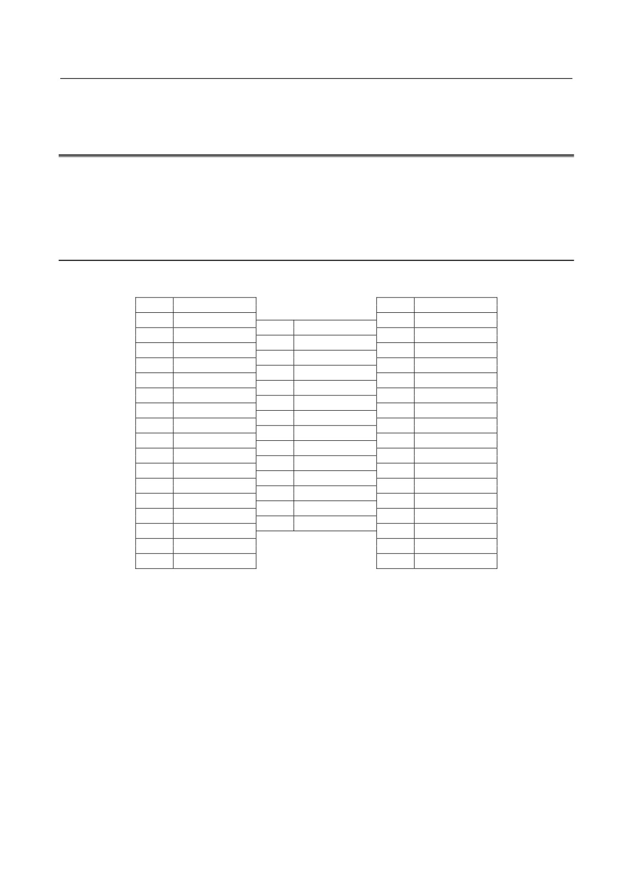
Given below are the details (signal arrangement diagrams as viewed from the front of the module) of the
connector pins and AOD16D3 terminal block for the I/O Units (32-point input module, 32-point output
module, and 24-point input/16-point output hybrid module) explained in Section 5.3.
5.5.1
Modules Using the MR-50RMA Connector Manufactured by
Honda Tsushin
• AID32A1/AID32B1/AID32H1 (32-point DC input module)
33
D7
01
D6
34
D5
02
D3
19
D4
35
D2
03
D0
20
D1
36
CMC
04
+24V
21
CMC
37
C7
05
GND
22
C6
38
C5
06
C3
23
C4
39
C2
07
C0
24
C1
40
CMC
08
+24V
25
41
CMC
09
GND
26
42
B7
10
B6
27
B4
43
B5
11
B3
28
B1
44
B2
12
B0
29
CMA
45
CMA
13
+24V
30
A6
46
A7
14
GND
31
A4
47
A5
15
A3
32
A1
48
A2
16
A0
49
CMA
17
+24V
50
CMA
18
GND
- 78 -
5.DIGITAL INPUT/OUTPUT
B-61813E/06
CONNECTION
MODULES
•
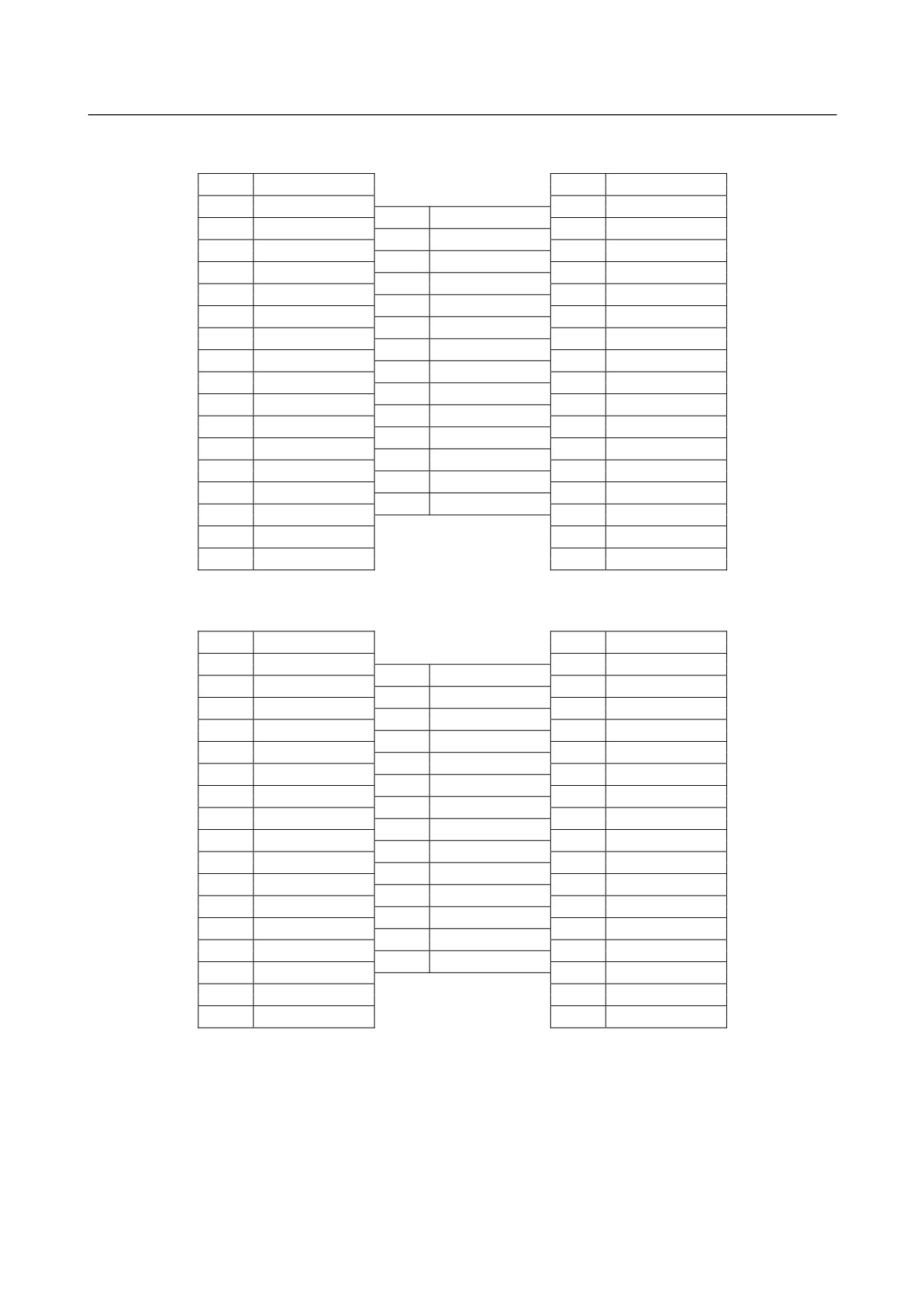
AID32E1/AID32F1 (32-point DC input module)
33
D7
01
D6
34
D5
02
D3
19
D4
35
D2
03
D0
20
D1
36
CMD
04
21
CMD
37
C7
05
22
C6
38
C5
06
C3
23
C4
39
C2
07
C0
24
C1
40
CMC
08
25
41
CMC
09
26
42
B7
10
B6
27
B4
43
B5
11
B3
28
B1
44
B2
12
B0
29
CMB
45
CMB
13
30
A6
46
A7
14
31
A4
47
A5
15
A3
32
A1
48
A2
16
A0
49
CMA
17
50
CMA
18
•
AOD32A1/AOD32C1 (32-point DC output module)
33
D7
01
D6
34
D5
02
D3
19
D4
35
D2
03
D0
20
D1
36
CMD
04
+24V-D
21
CMD
37
C7
05
22
C6
38
C5
06
C3
23
C4
39
C2
07
C0
24
C1
40
CMC
08
+24V-C
25
41
CMC
09
26
42
B7
10
B6
27
B4
43
B5
11
B3
28
B1
44
B2
12
B0
29
CMB
45
CMB
13
+24V-B
30
A6
46
A7
14
31
A4
47
A5
15
A3
32
A1
48
A2
16
A0
49
CMA
17
+24V-A
50
CMA
18
- 79 -
5. DIGITAL INPUT/OUTPUT
MODULES
CONNECTION
B-61813E/06
•
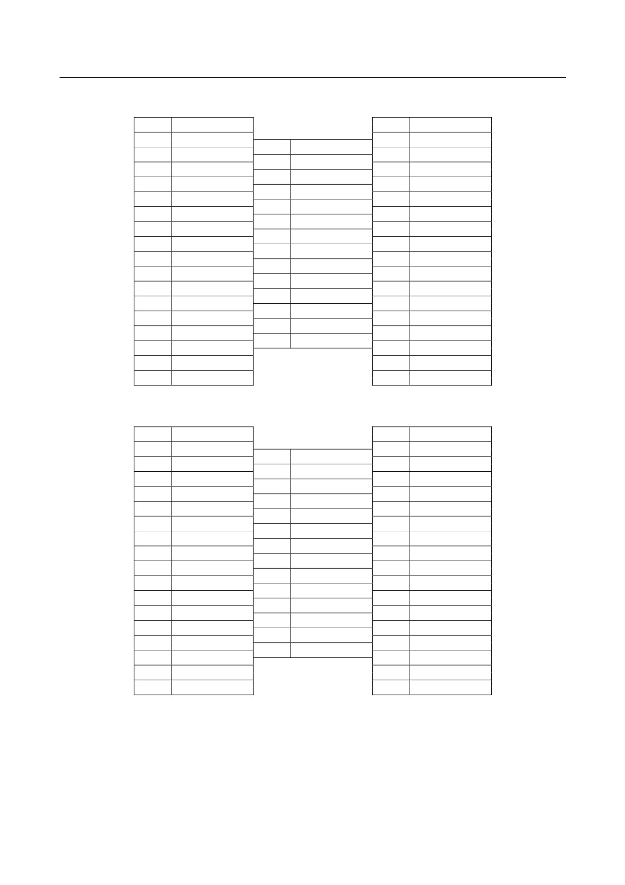
AOD32D1 (32-point DC output module)
33
D7
01
D6
34
D5
02
D3
19
D4
35
D2
03
D0
20
D1
36
CMD
04
21
CMD
37
C7
05
0V-D
22
C6
38
C5
06
C3
23
C4
39
C2
07
C0
24
C1
40
CMC
08
25
41
CMC
09
0V-C
26
42
B7
10
B6
27
B4
43
B5
11
B3
28
B1
44
B2
12
B0
29
CMB
45
CMB
13
30
A6
46
A7
14
0V-B
31
A4
47
A5
15
A3
32
A1
48
A2
16
A0
49
CMA
17
50
CMA
18
0V-A
•
AIO40A (24-point DC input/16-point DC output hybrid module)
33
B0
01
A0
34
B1
02
A1
19
C0
35
B2
03
A2
20
C1
36
B3
04
A3
21
C2
37
B4
05
A4
22
C3
38
B5
06
A5
23
C4
39
B6
07
A6
24
C5
40
B7
08
A7
25
C6
41
+24V
09
+24V
26
C7
42
F0
10
E0
27
CM
43
F1
11
E1
28
CMA
44
F2
12
E2
29
CMA
45
F3
13
E3
30
SP
46
F4
14
E4
31
0V
47
F5
15
E5
32
0V
48
F6
16
E6
49
F7
17
E7
50
0V
18
0V
- 80 -
5.DIGITAL INPUT/OUTPUT
B-61813E/06
CONNECTION
MODULES
5.5.2
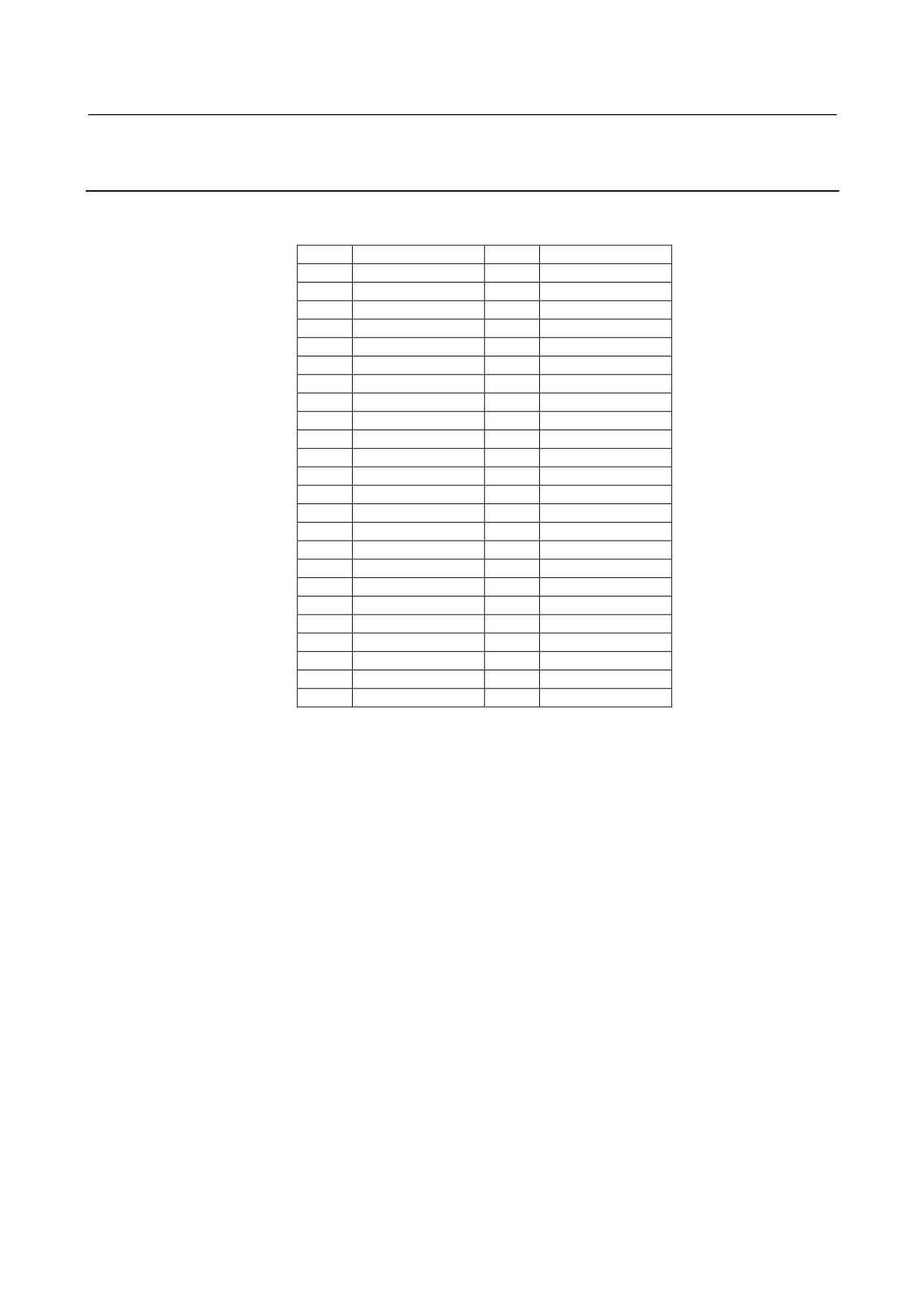
Modules Using the HIF3BB-50PA-2.54DS Connector
Manufactured by Hirose Electric
•
AID32E2/AID32F2 (32-point DC input module)
A01
B01
A02
D7
B02
D6
A03
D5
B03
D4
A04
D3
B04
D2
A05
D1
B05
D0
A06
CMD
B06
CMD
A07
B07
A08
C7
B08
C6
A09
C5
B09
C4
A10
C3
B10
C2
A11
C1
B11
C0
A12
CMC
B12
CMC
A13
B13
A14
B7
B14
B6
A15
B5
B15
B4
A16
B3
B16
B2
A17
B1
B17
B0
A18
CMB
B18
CMB
A19
B19
A20
A7
B20
A6
A21
A5
B21
A4
A22
A3
B22
A2
A23
A1
B23
A0
A24
CMA
B24
CMA
A25
B25
- 81 -
5. DIGITAL INPUT/OUTPUT
MODULES
CONNECTION
B-61813E/06
•
AOD32C2 (32-point DC output module)
A01
B01
+24V-D
A02
D7
B02
D6
A03
D5
B03
D4
A04
D3
B04
D2
A05
D1
B05
D0
A06
CMD
B06
CMD
A07
B07
+24V-C
A08
C7
B08
C6
A09
C5
B09
C4
A10
C3
B10
C2
A11
C1
B11
C0
A12
CMC
B12
CMC
A13
B13
+24V-B
A14
B7
B14
B6
A15
B5
B15
B4
A16
B3
B16
B2
A17
B1
B17
B0
A18
CMB
B18
CMB
A19
B19
+24V-A
A20
A7
B20
A6
A21
A5
B21
A4
A22
A3
B22
A2
A23
A1
B23
A0
A24
CMA
B24
CMA
A25
B25
•
AOD32D2 (32-point DC output module)
A01
0V-D
B01
A02
D7
B02
D6
A03
D5
B03
D4
A04
D3
B04
D2
A05
D1
B05
D0
A06
CMD
B06
CMD
A07
0V-C
B07
A08
C7
B08
C6
A09
C5
B09
C4
A10
C3
B10
C2
A11
C1
B11
C0
A12
CMC
B12
CMC
A13
0V-B
B13
A14
B7
B14
B6
A15
B5
B15
B4
A16
B3
B16
B2
A17
B1
B17
B0
A18
CMB
B18
CMB
A19
0V-A
B19
A20
A7
B20
A6
A21
A5
B21
A4
A22
A3
B22
A2
A23
A1
B23
A0
A24
CMA
B24
CMA
A25
B25
- 82 -
5.DIGITAL INPUT/OUTPUT
B-61813E/06
CONNECTION
MODULES
•
AOR16H2 (16-point relay output module)
A01
CMA
B01
CMA
A02
CMA
B02
CMA
A03
A0
B03
A0
A04
A1
B04
A1
A05
A2
B05
A2
A06
A3
B06
A3
A07
CMB
B07
CMB
A08
CMB
B08
CMB
A09
A4
B09
A4
A10
A5
B10
A5
A11
A6
B11
A6
A12
A7
B12
A7
A13
CMC
B13
CMC
A14
CMC
B14
CMC
A15
B0
B15
B0
A16
B1
B16
B1
A17
B2
B17
B2
A18
B3
B18
B3
A19
CMD
B19
CMD
A20
CMD
B20
CMD
A21
B4
B21
B4
A22
B5
B22
B5
A23
B6
B23
B6
A24
B7
B24
B7
A25
B25
5.5.3
Modules Using the HIF4-40P-3.18DS Connector Manufactured
by Hirose Electric
• AOD16D2 (16-point DC output module)
A01
A0
B01
0V-A
A02
A1
B02
0V-A
A03
A2
B03
CMA
A04
A3
B04
CMA
A05
CMA
B05
CMA
A06
A4
B06
0V-B
A07
A5
B07
0V-B
A08
A6
B08
CMB
A09
A7
B09
CMB
A10
CMB
B10
CMB
A11
CMC
B11
CMC
A12
B0
B12
CMC
A13
B1
B13
CMC
A14
B2
B14
0V-C
A15
B3
B15
0V-C
A16
CMD
B16
CMD
A17
B4
B17
CMD
A18
B5
B18
CMD
A19
B6
B19
0V-D
A20
B7
B20
0V-D
- 83 -
5. DIGITAL INPUT/OUTPUT
MODULES
CONNECTION
B-61813E/06
5.5.4
Modules Using the Terminal Block BL3.5/24/90F Manufactured
by Weidmüller
•
AOD16D3 (16-point DC output module)
01
CMA
02
A0
03
A1
04
A2
05
A3
06
0V-A
07
CMB
08
A4
09
A5
10
A6
11
A7
12
0V-B
13
CMC
14
B0
15
B1
16
B2
17
B3
18
0V-C
19
CMD
20
B4
21
B5
22
B6
23
B7
24
0V-D
- 84 -
B-61813E/06
CONNECTION
6.ANALOG INPUT MODULE
6 ANALOG INPUT MODULE
6.1
12-BIT ANALOG INPUT MODULE (AAD04A)
6.1.1
Specifications
Item
Specifications
Number of input channel
4 channel/module
Analog input
• Voltage input
-10VDC to+10VDC(input resistance 4.7MΩ)
• Current input
-20mADC to+20mADC(input resistance 250Ω)
Caution) Which method to use, voltage input or current input, can be selected by
connecting the corresponding input to the terminal block.
Digital output
12 bit binary (complementary representation of "2".)
Input/output correspondence
Analog input
Digital output
+10V
+2000
+5V or + 20mA
+1000
0V or 0mA
0
-5V or -20mA
-1000
-10V
-2000
Resolution
5mV or 20μA
Total precision
Voltage input ±0.5%(For full scale)
Current input ±1%(For full scale)
Conversionary time
Max.2ms (Note)
Maximum input voltage/current
±15V, ±30mA
Isolation
Photocoupler isolated (between the input signal and the base)
However, not isolated between input channels
Output connecting
Removable terminal block (20 terminals, M3.5 screw terminal)
Required input points
64 points
NOTE
Conversion time means that only in a module. Actual response speed is
determined by adding the scanning time depending on each system to this
conversion time.
- 85 -
6.ANALOG INPUT MODULE
CONNECTION
B-61813E/06
6.1.2
Correspondence between Input Signals and Addresses in a
Module
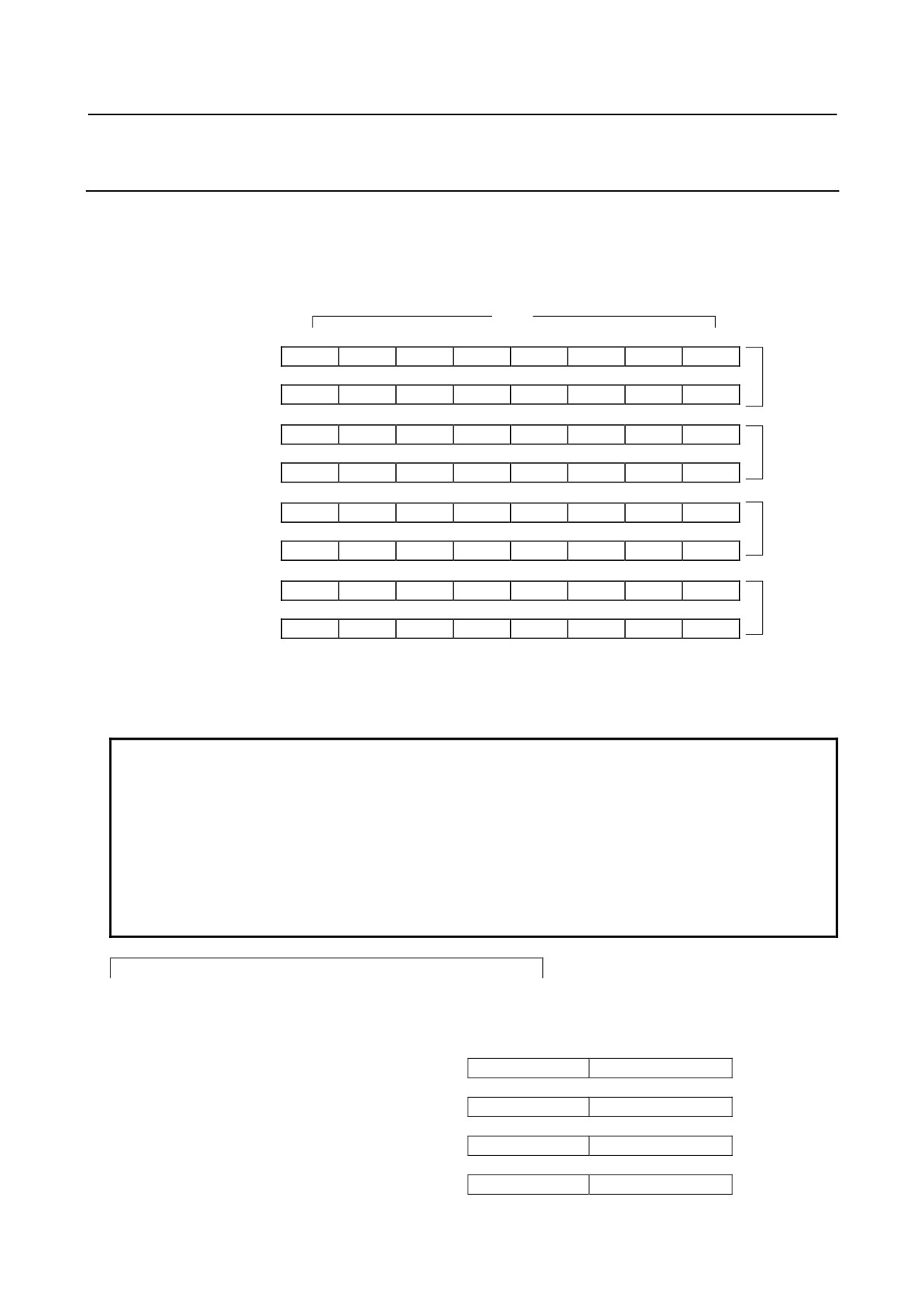
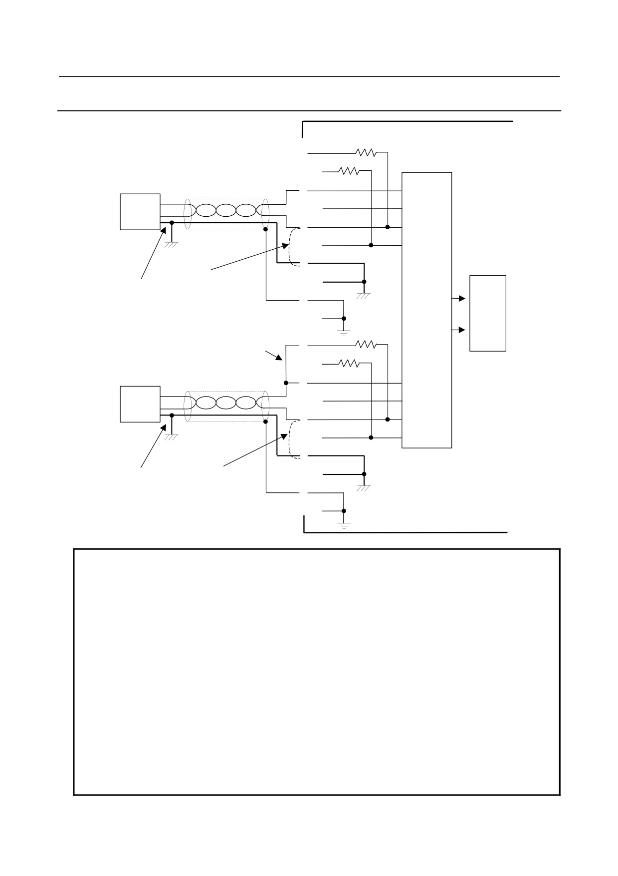
In the analog input module AAD04A, the 4-channel analog input signals are cyclically A-D converted in
order, and the converted digital data are written in the following addresses. Therefore, in the PMC program,
it is possible at any time to know the values for the analog input signals by referring to the following
addresses.
Address
Bits
in module
7
6
5
4
3
2
1
0
0
D07-0
D06-0
D05-0
D04-0
D03-0
D02-0
D01-0
D00-0
Channel 0
1
X-0
X-0
X-0
X-0
D11-0
D10-0
D09-0
D08-0
2
D07-1
D06-1
D05-1
D04-1
D03-1
D02-1
D01-1
D00-1
Channel 1
3
X-1
X-1
X-1
X-1
D11-1
D10-1
D09-1
D08-1
4
D07-2
D06-2
D05-2
D04-2
D03-2
D02-2
D01-2
D00-2
Channel 2
5
X-2
X-2
X-2
X-2
D11-2
D10-2
D09-2
D08-2
6
D07-3
D06-3
D05-3
D04-3
D03-3
D02-3
D01-3
D00-3
Channel 3
7
X-3
X-3
X-3
X-3
D11-3
D10-3
D09-3
D08-3
D00-n and D11-n correspond to the weights of 20 and 211 respectively. Here, D11-n corresponds to the sign
bit in the complementary representation of "2."
In addition, in X-n is written the same value as that in D11-n.
NOTE
1 I/O Link requires that the start address of each I/O module be even-numbered.
Moreover, when an A-D converted value is referred to in a PMC program, make
sure to read the data in unit of a word (16 bits).
2 I/O Link i does not care whether the start address of this module is even- or
odd-numbered.
3 Note that on the PMC-N, -NA, and -QA (PMC for the Series 15 (Series 15
preceding the i series) and F-D Mate), the high-order one byte and low-order one
byte of a word (16 bits) are interchanged with each other as described below.
Addresses for word-unit operation in the PMC-N, NA, and QA
Analog input module → PMC
Address in the module High-order byte
Low-order byte
Channel 0
0
D07-0 to D00-0
X-0,D11-0 to D08-0
Channel 1
+2
D07-1 to D00-1
X-1,D11-1 to D08-1
Channel 2
+4
D07-2 to D00-2
X-2,D11-2 to D08-2
Channel 3
+6
D07-3 to D00-3
X-3,D11-3 to D08-3
- 86 -
B-61813E/06
CONNECTION
6.ANALOG INPUT MODULE
6.1.3
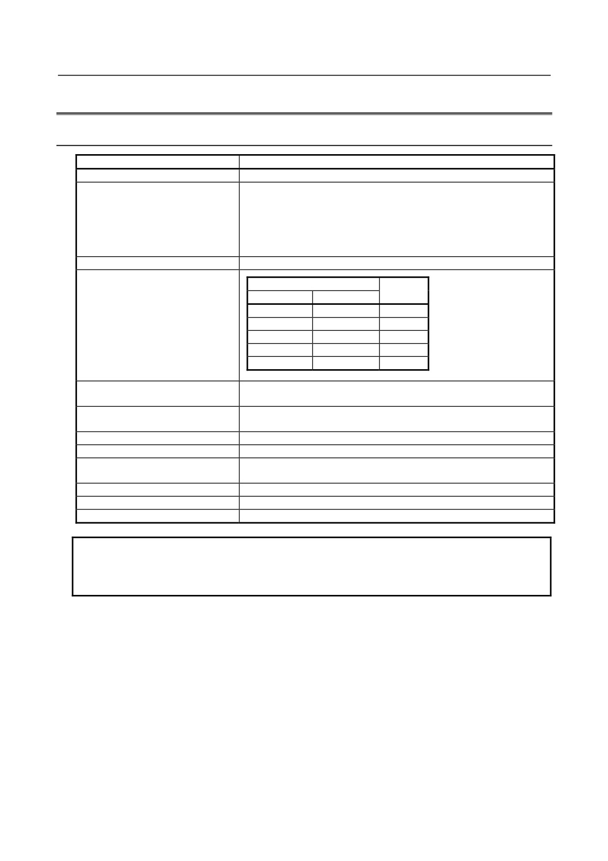
Connecting with Analog Input Module
Analog input module (AAD04A)
I0+
①
I1+
250Ω
②
V0+
Voltage input (channel0)
③
+
V1+
Voltage
supply
④
-
V0-
GND
⑤
V1-
Multi
⑥
processor
COM0
⑦
Note
COM1
Note
4-2
⑧
AD
4-1
FG0
converter
⑨
FG1
⑩
I2+
250Ω
Note 2
⑪
I3+
⑫
V2+
Current input (channel 2)
⑬
Current
+
V3+
supply
-
⑭
V2-
GND
⑮
V3-
⑯
COM2
⑰
COM3
Note
Note
⑱
4-1
4-2
FG2
⑲
FG3
⑳
NOTE
1 Though the example above shows the connection of channels 0 and 2, it is just the
same with the channel 1 (I1+, V1+, V1-, COM1 and FG1) and the channel 3 (I3+,
V3+, V3-, COM3 and FG3).
2 Either voltage input or current input can be specified for each channel. When
current input is specified, make sure to short-circuit in + and Vn+ (n: 0 to 3).
3 Use shielded cables of twisted pair for connecting.
4 Fix a reference voltage by connecting the COMn (where n is 0, 1, 2, or 3) terminal
of this module to the common line (GND) of the voltage or current source to be
used as shown above.
5 If the voltage or current source has a terminal shared by the external output
(terminal OUT-) and ground (GND), the Vn- and COMn (where n is 0, 1, 2, or 3) of
this module can be connected to each other as shown above.
6 The shielding wires are ground in the AAD04A. However, both ends grounding or
both ends opening may be more effective depending on the environment where
the unit is used. Select one of the grounding types, whichever is appropriate,
depending on what the ambient noise is like.
- 87 -
6.ANALOG INPUT MODULE
CONNECTION
B-61813E/06
6.2
16-BIT ANALOG INPUT MODULE (AAD04B)
6.2.1
Specifications
Item
Specifications
Number of input channel
4 channel/module
Analog input
• Voltage input
-10VDC to+10VDC(input resistance 4.7MΩ)
• Current input
-20mADC to+20mADC(input resistance 250Ω)
Caution) Which method to use, voltage input or current input, can be selected
by connecting the corresponding input to the terminal block.
Digital output
16 bit binary (complementary representation of "2".)
Input/output correspondence
Analog input
Digital
Voltage input
Current input
output
+10V
-
+32000
+5V
+20mA
+16000
0
0
0
-5V
-20mA
-16000
-10V
-
-32000
Resolution
Voltage input: 0.3125mV
Current input: 1.25μA
Total precision
Voltage input: ±0.5%(For full scale)
Current input: ±1%(For full scale)
Conversionary time
Max.2ms (Note)
Maximum input voltage/current
±15V, ±30mA
Isolation
Photocoupler isolated (between the input signal and the base)
However, not isolated between input channels
Output connecting
Removable terminal block(20 terminals, M3.5 screw terminal)
Required input points
64 points
Name assigned to module
“AD04A” or “/8”
NOTE
Conversion time means that only in a module. Actual response speed is
determined by adding the scanning time depending on each system to this
conversion time.
- 88 -
B-61813E/06
CONNECTION
6.ANALOG INPUT MODULE
6.2.2
Correspondence between Input Signals and Addresses in a
Module
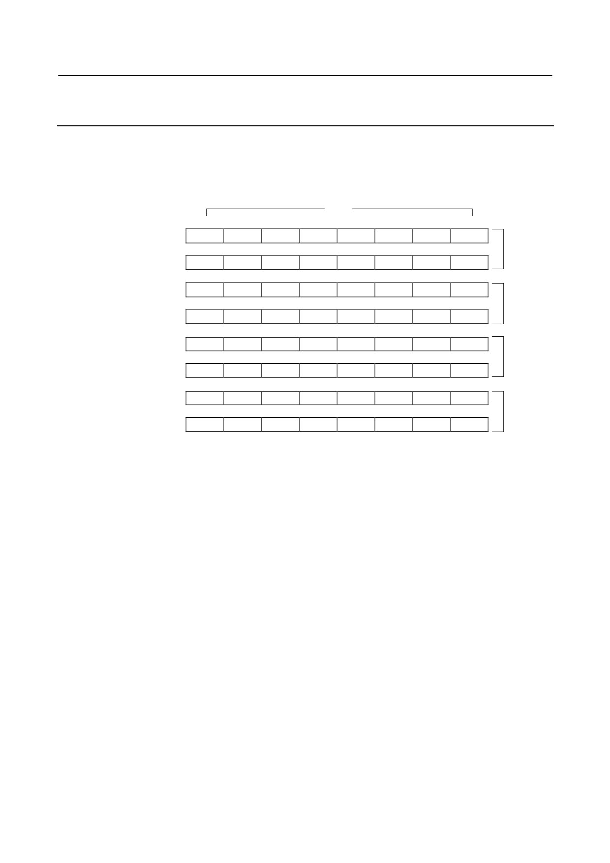
In the analog input module AAD04B, the 4-channel analog input signals are cyclically A-D converted in
order, and the converted digital data are written in the following addresses. Therefore, in the PMC program,
it is possible at any time to know the values for the analog input signals by referring to the following
addresses.
Address
Bits
in module
7
6
5
4
3
2
1
0
0
D07-0
D06-0
D05-0
D04-0
D03-0
D02-0
D01-0
D00-0
Channel 0
1
D15-0
D14-0
D13-0
D12-0
D11-0
D10-0
D09-0
D08-0
2
D07-1
D06-1
D05-1
D04-1
D03-1
D02-1
D01-1
D00-1
Channel 1
3
D15-1
D14-1
D13-1
D12-1
D11-1
D10-1
D09-1
D08-1
4
D07-2
D06-2
D05-2
D04-2
D03-2
D02-2
D01-2
D00-2
Channel 2
5
D15-2
D14-2
D13-2
D12-2
D11-2
D10-2
D09-2
D08-2
6
D07-3
D06-3
D05-3
D04-3
D03-3
D02-3
D01-3
D00-3
Channel 3
7
D15-3
D14-3
D13-3
D12-3
D11-3
D10-3
D09-3
D08-3
D00-n and D15-n correspond to the weights of 20 and 215 respectively. Here, D15-n corresponds to the sign
bit in the complementary representation of "2." (where n represents one of the channel numbers 0 to 3)
- 89 -
6.ANALOG INPUT MODULE
CONNECTION
B-61813E/06
NOTE
1 I/O Link requires that the start address of each I/O module be even-numbered.
Moreover, when an A-D converted value is referred to in a PMC program, make
sure to read the data in unit of a word (16 bits).
2 I/O Link i does not care whether the start address of this module is even- or
odd-numbered.
3 This module has a very high resolution. When A-D converted values are input to
a system for reference by the PMC program, they may disperse largely depending
on the system. If this is the case, the dispersion of input values can be suppressed
by obtaining their moving average in the PMC program or lowering the resolution
by masking the lowest-order bit if possible.
4 Note that on the PMC-N, -NA, and -QA (PMC for the Series 15 (Series 15
preceding the i series) and F-D Mate), the high-order one byte and low-order one
byte of a word (16 bits) are interchanged with each other as described below.
Addresses for word-unit operation in the PMC-N, NA, and QA
Analog input module → PMC
Address in the module High-order byte
Low-order byte
Channel 0
0
D07-0 to D00-0
D15-0 to D08-0
Channel 1
+2
D07-1 to D00-1
D15-1 to D08-1
Channel 2
+4
D07-2 to D00-2
,D15-2 to D08-2
Channel 3
+6
D07-3 to D00-3
D15-3 to D08-3
- 90 -
B-61813E/06
CONNECTION
6.ANALOG INPUT MODULE
6.2.3
Connecting with Analog Input Module
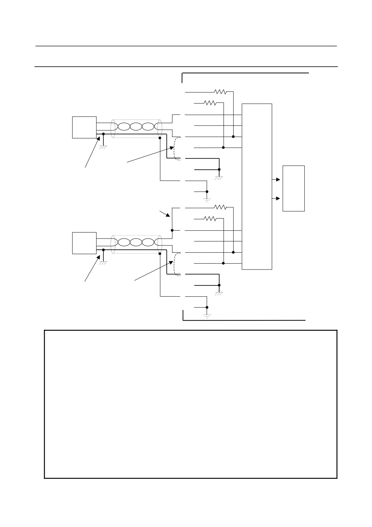
Analog input module (AAD04B)
I0+
①
I1+
250Ω
②
V0+
Voltage input (channel0)
③
+
V1+
Voltage
supply
④
-
V0-
GND
⑤
V1-
Multi
⑥
processor
COM0
⑦
Note
COM1
Note
4-2
⑧
AD
4-1
FG0
converter
⑨
FG1
⑩
I2+
250Ω
Note 2
⑪
I3+
⑫
V2+
Current input (channel 2)
⑬
Current
+
V3+
supply
-
⑭
V2-
GND
⑮
V3-
⑯
COM2
⑰
COM3
Note
Note
⑱
4-1
4-2
FG2
⑲
FG3
⑳
NOTE
1 Though the example above shows the connection of channels 0 and 2, it is just the
same with the channel 1 (I1+, V1+, V1-, COM1 and FG1) and the channel 3 (I3+,
V3+, V3-, COM3 and FG3).
2 Either voltage input or current input can be specified for each channel. When
current input is specified, make sure to short-circuit in + and Vn+ (n: 0 to 3).
3 Use shielded cables of twisted pair for connecting.
4 Fix a reference voltage by connecting the COMn (where n is 0, 1, 2, or 3) terminal
of this module to the common line (GND) of the voltage or current source to be
used as shown above.
5 If the voltage or current source has a terminal shared by the external output
(terminal OUT-) and ground (GND), the Vn- and COMn (where n is 0, 1, 2, or 3) of
this module can be connected to each other as shown above.
6 The shielding wires are ground in the AAD04B. However, both ends grounding or
both ends opening may be more effective depending on the environment where
the unit is used. Select one of the grounding types, whichever is appropriate,
depending on what the ambient noise is like.
- 91 -
7.ANALOG OUTPUT MODULE
CONNECTION
B-61813E/06
7 ANALOG OUTPUT MODULE
7.1
12-BIT ANALOG OUTPUT MODULE (ADA02A)
7.1.1
Specification
Item
Specification
Number of output channels
2 channels/module
Digital input
12-bit binary (2's complement representation)
Analog output
-10VDC to +10VDC(external load resistance: 10KΩ or more) (Note 1)
0mADC to +20mADC(external load resistance: 400Ω or less)
Input/output correspondence
Digital input
Analog output
+2000
+10V
+1000
+5V or +20mA
0
0V or 0mA
-1000
-5V
-2000
-10V
Resolution
5mV or 20μA
Comprehensive accuracy
Voltage output: ±0.5% (For the full scale)
Current output: ±1% (For the full scale)
Converting time
1msec or less (Note 2)
Insulation
Photocoupler insulation (between output signal and base).
However, non-insulation between output channels.
External connection
At removable terminal block (20 terminals, M3.5 screw terminals)
Number of occupied output points
32 points
NOTE
1 Which method to use, voltage input or current input, can be selected by
connecting the corresponding input to the terminal block.
2 The converting time is the one only inside the module. The actual response time is
added a scan time that is determined by the system.
3 If this module is connected to any unit that requires a separate power supply, turn
on the I/O Unit-A before that unit. Turning on that unit before the I/O Unit-A may
lead to an accident dew to incorrect output or malfunction.
- 92 -
B-61813E/06
CONNECTION
7.ANALOG OUTPUT MODULE
7.1.2
Correspondence between Output Signals and Addresses in a
Module
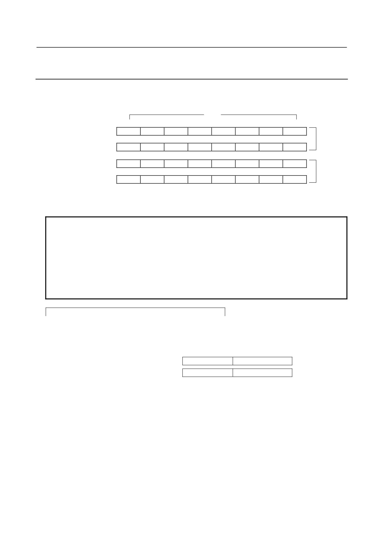
In the analog output module ADA02A, a 12-bit digital value is written into each of the following addresses
to output the desired voltage/current to its corresponding analog output.
Address
Bits
in module
7
6
5
4
3
2
1
0
0
D07-0
D06-0
D05-0
D04-0
D03-0
D02-0
D01-0
D00-0
Channel 0
1
-
-
-
-
D11-0
D10-0
D09-0
D08-0
2
D07-1
D06-1
D05-1
D04-1
D03-1
D02-1
D01-1
D00-1
Channel 1
3
-
-
-
-
D11-1
D10-1
D09-1
D08-1
D00-n corresponds to the 20 weight, while D11-n corresponds to the 211 weight.
However, D11-n corresponds to the code bit 2's complement representation.
NOTE
1 I/O Link requires that the start address of each I/O module be even-numbered. To
write a value that is to be converted from digital to analog into a PMC program, be
sure to write it in words (16 bits).
2 I/O Link i does not care whether the start address of this module is even- or
odd-numbered.
3 Note that on the PMC-N, -NA, and -QA (PMC for the Series 15 (Series 15
preceding the i series) and F-D Mate), the high-order one byte and low-order one
byte of a word (16 bits) are interchanged with each other as described below.
Addresses for word-unit operation in the PMC-N, NA, and QA
PMC → 12-bit analog output module
Module in
address
High-order byte
Low-order byte
Channel 0
0
D07-0 to D00-0
D11-0 to D08-0
Channel 1
+2
D07-1 to D00-1
D11-1 to D08-1
- 93 -
7.ANALOG OUTPUT MODULE
CONNECTION
B-61813E/06
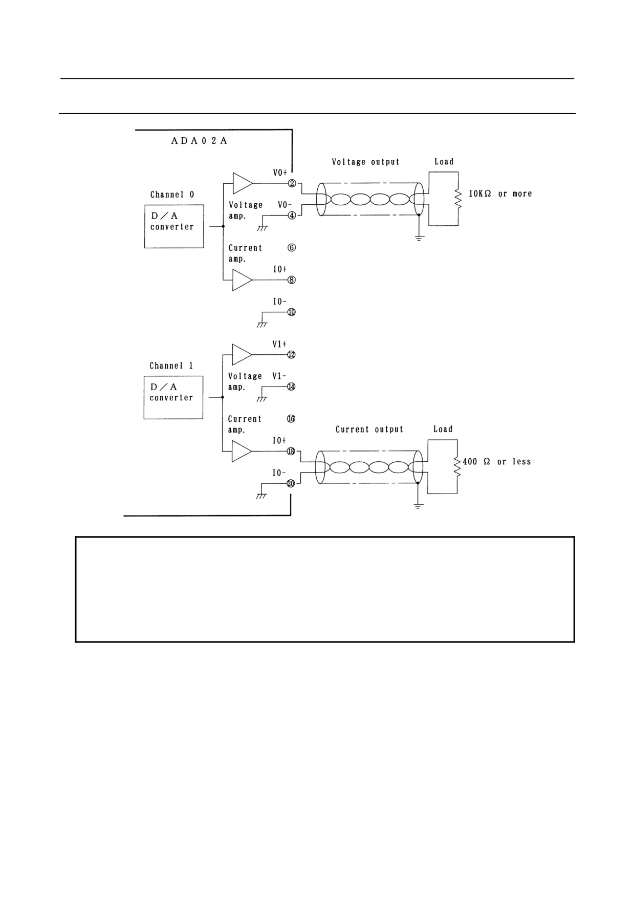
7.1.3
Connection to Analog Output Module
NOTE
1 Use a 2-core twisted shielded cable as the connection cable
2 Ground the shielding wire of the cable only at one point on the load side
(single-point grounding). However, both ends grounding or both ends opening
may be more effective depending on the environment where the unit is used.
Select one of the grounding types, whichever is appropriate, depending on what
the ambient noise is like.
- 94 -