Loongson 3A3000/3B3000 processor user manual. Part ii GS464E processor core V1.2 - page 1
Loongson 3A3000/3B3000 processor
user manual
Part ii
GS464E processor core V1.2
In December 2017
Loongson Zhongke Technology Co. LTD
The godson 3 A3000/3B3000 ChuLiQiYongHuShouCe
vol.6
Copyright statement
The copyright of this document belongs to Loongson Technology Co., LTD., and all rights are reserved. No
company or individual may publish, reprint or otherwise distribute any part of this document to third parties
without written permission. Otherwise, it will be investigated for legal responsibility.
disclaimer
This document only provides phased information. The contents can be updated according to the actual situation of
the product at any time without prior notice. The Company shall not be liable for any direct or indirect losses
caused by improper use of documents.
Loongson Zhongke Technology Co. LTD
Loongson Technology Corporation Limited
Address: Loongson Industrial Park, Building No.2, Loongson Industrial Park, Zhongguancun Environmental
Protection Technology Demonstration Park, Haidian District, Beijing
Zhongguancun Environmental Protection Park, Haidian District, Beijing
Tel: 010-62546668 Fax: 010-62600826
Reading guide
The User manual of Loongson 3A3000/3B3000 processor is divided into the first and the second volumes.
The second volume of The User's Manual of The 3A300/3B3000 processor introduces in detail the GS464E high-
performance processor core used by the 3A300/3B3000 processor from the perspective of system software
developers.
Special format meaning introduction
1. When the description of a Field of CP0 control register is involved in this document, the format of reg. Field is
adopted, in which Reg is the mnemonic of the control register and Field is the mnemonic of the Field to be
described in the storage. For example, Ebase.cpunum represents the CPUNum field of the EBase control register.
2. The description of data content interception in this document is in the format of [m:n] or, indicating that the NTH
bit to m of the content to be intercepted is selected m..n
position M, n starts at 0, m is greater than or equal to n.
Version history
Loongson 3A3000/3B3000 processor
Document update record
The
user manual
document
- part ii
name:
The
V1.2
version
number
The
Chip R&d Department
founders:
Date created:
2017-12-20
Update history
The
Updated
Update one
The
Update
serial
date
version
the
num
numbe
content
ber
r
1
2017/04/07
Chip R&d
V1.0
The first draft is complete.
Department
1. Fixed an error in the instruction list in Chapter 2.
2
2017/11/29
Chip R&d
V1.1
Department
2. Section 2.3.1 adds the list of "DSP instructions no longer
supported by MIPS"
3
2017/12/20
Chip R&d
V1.2
Fixed 8 instructions in the instruction list in Chapter 2.
Department
Technical support
You can submit the problems of product use to our company through email or
problem feedback website, and obtain technical support. After-sales Service
Email: service@loongson.cn
Question feedback web site: http://bugs.loongnix.org/
directory
目录
1
Overview of processor core structure
12
1.1 Speed overview of processor core structure parameters
15
2
Instruction set Overview
5
2.1
MIPS64 compatible General instruction list
5
2.1.1
To fetch instruction
5
2.1.2
Operation instruction
7
2.1.3
Jump and branch instructions
9
2.1.4
Coprocessor 0 instruction
11
2.2
MIPS64 is compatible with floating point instruction set overview
14
2.2.1
FPU data type
14
2.2.2
Floating point register
17
2.2.3
Floating point control register
17
2.2.4
Floating-point exception
17
2.2.5
MIPS64 is compatible with floating point instruction list
21
2.3
An overview of THE MIPS64 DSP instruction set
26
2.3.1
MIPS64 DSP ASE compatible instruction list
27
2.3.2
Supplementary instructions to MIPS DSP instruction manual
47
2.4
MIPS64 compatible instruction implementation definition
47
2.4.1
The load instruction that targets the no. 0 general purpose register
47
2.4.2
PREF instruction
47
2.4.3
RDHWR instruction
47
2.4.4
PREFX instruction
47
2.4.5
WAIT instruction
49
2.4.6
SYNC instructions
49
2.4.7
SYNCI instruction
49
2.4.8
TLBINV and TLBINVF directives
49
2.4.9
CACHE directives
50
2.4.10
Madd.fmt, Msub.fmt, Nmadd.fmt, Nmsub.fMT instruction
52
2.4.11
EHB, SSNOP instructions
53
2.4.12
DI and EI instructions
53
2.5
Loong core expansion command set
53
3
Processor running mode
72
3.1
Processor run mode definition
72
3.1.1
Debug mode
72
3.1.2
The root-core pattern
72
3.1.3
Root-user mode
73
4
Memory management
47
4.1
The basic concept
47
4.1.1
Address space
47
4.1.2
Segment and segment size (SEGBITS)
47
4.1.3
Physical Address size (PABITS)
47
4.1.4
Mapped Address and Unmapped Address
47
4.2
Host virtual address space
47
4.2.1
Host address space division and access control
47
I
4.2.2
The address translation, cacheability and cache consistency of host address space Kseg0 segment and Kseg1
segment
50
4.2.3
The address translation and cacheability of the host address space Xkphys segment are consistent with the cache
properties
50
4.2.4
Address translation of the kusEG segment of the host address space when status.erl =1
50
4.2.5
Special treatment of host address space kseg3 when debug.dm =1
51
4.2.6
Special handling of data access to virtual addresses when status.ux =0 in user mode
51
4.3
TLB - based virtual and real address mapping
50
4.3.1
TLB hierarchy
50
4.3.2
JTLB structure
51
4.3.3
JTLB table item
52
4.3.4
TLB software management
53
4.3.5
TLB initialization and clearing
53
4.3.6
TLB - based virtual address translation process
54
5
Organization and management of caches
59
5.1
Processor storage hierarchy and cache hierarchy
59
5.1.1
Processor storage hierarchy
59
5.1.2
Level 1 instruction Cache (I-cache)
61
5.1.3
Level 1 data Cache (D-Cache)
63
5.1.4
Level 2 Sacrifice Cache (V-Cache)
64
5.1.5
Level 3 Shared Cache (S-Cache)
66
5.2
The cache algorithm has the same properties as the cache
68
5.2.1
Non-cache algorithm
68
5.2.2
Consistent caching algorithm
68
5.2.3
Non-cache acceleration algorithm
68
5.3
Cache consistency
69
5.4
Cache management
70
5.4.1
CACHE directives
70
5.4.2
Cache initialization
67
5.4.3
Maintain consistency between level 1 instruction cache and level 1 data cache
70
5.4.4
Maintain cache consistency between processor and DMA device
70
5.4.5
Cache alias and page coloring
70
6
Processor exceptions and interrupts
72
6.1
Processor exception
72
6.1.1
Exception priority
72
6.1.2
Exception entry vector position
72
6.1.3
The processor hardware responds to the exception's generic processing
74
6.1.4
Cold reset exception
75
6.1.5
Non-masking interrupt
76
6.1.6
Interrupt exception
76
6.1.7
Wrong address exception
76
6.1.8
TLB rewrites the exception
78
6.1.9
XTLB rewrites the exception
78
6.1.10
TLB is not an exception
80
6.1.11
TLB modification exceptions
76
6.1.12
TLB performs blocking exceptions
76
6.1.13
TLB reads prevent exceptions
78
6.1.14
Cache error exception
78
6.1.15
Exception for integer overflow
78
II
6.1.16
Trap exceptions
78
6.1.17
System call exception
78
6.1.18
Breakpoint exception
78
6.1.19
Reservation instruction exception
79
6.1.20
No exceptions can be made to the coprocessor
80
6.1.21
Floating-point exception
80
6.1.22
Floating point stack exception
80
6.2
interrupt
80
6.2.1
Requirements for interrupt response
80
6.2.2
Interrupt mode
80
6.2.3
Additional notes on interrupt handling
84
7
Coprocessor register 0
86
7.1
Root coprocessor 0 register overview
86
7.2
Index Register (CP0 Register 0, Select 0)
85
7.3
Random Register (CP0 Register 1, Select 0)
86
7.4
EntryLo0 and EntryLo1 registers (CP0 Register 2 and 3, Select 0)
87
7.5
Context Register (CP0 Register 4, Select 0)
90
7.6
UserLocal Register (CP0 Register 4, Selelct 2)
91
7.7
PageMask Register (CP0 Register 5, Select 0)
92
7.8
PageGrain Register (CP0 Register 5, Select 1)
94
7.9
PWBase Register (CP0 Register 5, Select 5)
96
7.10
PWField Register (CP0 Register 5, Select 6)
98
7.11
PWSize Register 5, Select 6
100
7.12
Wired Register (CP0 Register 6, Select 0)
102
7.13
PWCtl Register 6, Select 6
103
7.14
Trade characters for a Register (CP0 Register 7, Select 0)
104
7.15
BadVAddr Register (CP0 Register 8, Select 0)
105
7.16
Count Register 9, Select 0
106
7.17
GSEBase Register (CP0 Register 9, Select 6)
107
7.18
PGD Register (CP0 Register 9, Select 7)
108
7.19
EntryHi Register (CP0 Register 10, Select 0)
109
7.20
Compare Register (CP0 Register 11, Select 0)
106
7.21
Status Register (CP0 Register 12, Select 0)
107
7.22
IntCtl Register (CP0 Register 12, Select 1)
109
7.23
SRSCtl Register (CP0 Register 12, Select 2)
110
7.24
Cause Register (CP0 Register 13, Select 0)
111
7.25
EPC Register (CP0 Register 14, Select 0)
113
7.26
PRId Register (CP0 Register 15, Select 0)
114
7.27
EBase Register (CP0 Register 15, Select 1)
115
7.28
Config Register (CP0 Register 16, Select 0)
116
7.29
Config1 Register (CP0 Register 16, Select 1)
117
7.30
Config2 Register (CP0 Register 16, Select 2)
118
7.31
Config3 Register (CP0 Register 16, Select 3)
119
7.32
Config4 Register (CP0 Register 16, Select 4)
121
7.33
Config5 Register (CP0 Register 16, Select 5)
123
7.34
GSConfig Register (CP0 Register 16, Select 6)
124
7.35
LLAddr Register (CP0 Register 17, Select 0)
127
7.36
XContext Register (CP0 Register 20, Select 0)
128
7.37
Diag Register (CP0 Register 22, Select 0)
130
III
7.38
GSCause Register (CP0 Register 22, Select 1)
131
7.39
VPID Register (CP0 Register 22, Select 2)
132
7.40
Debug Register (CP0 Register 23, Select 0)
133
7.41
DEPC Register (CP0 Register 24, Select 0)
134
7.42
PerfCnt Register (CP0 Register 25, Select 0~7)
135
7.43
ErrCtl Register (CP0 Register 26, Select 0)
137
7.44
CacheErr Register (CP0 Register 27, Select 0)
138
7.45
CacheErr1 Register (CP0 Register 27, Select 1)
140
7.46
TagLo register (CP0 Register28, Select 0)
141
7.47
DataLo Register (CP0 Register 28, Select 1)
144
7.48
TagHi Register (CP0 Register 29, Select 0)
145
7.49
DataHi Register (CP0 Register 29, Select 1)
146
7.50
ErrorEPC Register (CP0 Register 30, Select 0)
147
7.51
DESAVE Register (CP0 Register 31, Select 0)
148
7.52
KScratch1~6 registers (CP0 Register 31, Select 2~7)
149
8
Analysis and optimization of processor performance
150
8.1
Organization and access method of performance counters
150
8.1.1
Processor core performance counter
150
8.1.2
Shared cache performance counters
150
8.2
Processor performance count events
151
8.2.1
Processor core performance count event definition
151
8.2.2
Shared cache performance count event definition
167
IV
Figure directory
Figure 2-1 FPU floating point data format 11
Figure 2-2 FPU fixed-point data format 13
Figure 2-3 FIR register format 13
Figure 2-4. FCSR register format 14
Figure 2-5 FCCR register format 15
Figure 2-6 FEXR register format 16
Figure 2-7 FENR register format 16
Figure 2-8. Address resolution format of the Index class CACHE instruction 34
Figure 4-1 Xkphys segment virtual address resolution method 49
Figure 5-1 Longson 3A3000 chip processor storage level 59
Figure 5-2. Structure of level 1 instruction cache line is 60
Figure 5-3 The row structure of the first-level data cache is 61
Figure 5-4 Shows the second-level sacrifice cache row structure for 62
Figure 5-5 Shows the three-level Shared cache row structure for 64
Figure 5-6 Cache state transition under conformance protocol 65
Figure 7-1. Index register format 85
Figure 7-2. Random register format 86
Figure 7-3 Register format 87 for THE DMFC0/DMTC0 instruction access for EntryLo0 and EntryLo1
Figure 7-4 Register format 88 for EntryLo0 and EntryLo1 when accessed by the MFC0/MTC0 instructions
Figure 7-5 Context register format 90
Figure 7-6 UserLocal register format 91
Figure 7-7 PageMask register format 92
Figure 7-8 PageGrain register format 93
Figure 7-9 Page table access process 94 supported by PWBase,PWField,PWSize and PWCtl .
Figure 7-10. PWBase register format 94
Figure 7-11. PWField register format 95
Figure 7-12. PWSize register format 96
Figure 7-13 Fixed table entry and random replacement table entry boundary in VTLB 97 .
Figure 7-14 Wired register format 97
Figure 7-15 PWCtl register format 98
Figure 7-16 For trade A register format 99
Figure 7-17 BadVAddr register format 100
Figure 7-18. Count register format 101
Figure 7-19 GSEBase register format 102
Figure 7-20 PGD register format 103
Figure 7-21. EntryHi register format 104
Figure 7-22 Compare register format 106
Figure 7-23 Status register format 107
Figure 7-24 IntCtl register format 109
Figure 7-25 SRSCtl register format 110
Figure 7-26 Cause register format 111
V
Figure 7-27 EPC register format 113
VI
Figure 7-28 PRId register format 114
Figure 7-29 EBase register format 115
Figure 7-30. Config register format 116
Figure 7-31 Config1 register format 117
Figure 7-32 Config2 register format 118
Figure 7-33 Config3 register format 119
Figure 7-34 Config4 register format 121
Figure 7-35. Config5 register format 123
Figure 7-36 GSConfig register format 124
Figure 7-37. LLAddr register format 127
Figure 7-38 XContext register format 128
Figure 7-39 Diag register format 129
Figure 7-40 GSCause register format 131
Figure 7-41 VPID register format 132
Figure 7-42 DEPC register format 134
Figure 7-43 PerfCnt Control register format 135
Figure 7-44 PerfCnt Counter register format 136
Figure 7-45 ErrCtl register format 137
Figure 7-46 CacheErr register format 138 when used for I-Cache error-checking information
Figure 7-47 CacheErr register format 138 when used for D-Cache error-checking information
Figure
7-48 CacheErr1 register format 140
Figure
7-49 The TagLo register is used to access the I-Cache Tag in format 141
Figure
7-50 TagLo register is used for format 141 when accessing the D-Cache Tag
Figure
7-51 TagLo register in format 142 for accessing the V-Cache Tag
Figure
7-52 The TagLo register is used to access the S-Cache Tag in format 142
Figure 7-53. The TagLo register is in format 143 for accessing each level of Cache Data
Figure 7-54 The DataLo register is used for i-Cache access in format 144
Figure 7-55 Shows the format 145 of the TagHi register used to access the various Cache tags
Figure 7-56 The TagHi register is in format 145 for accessing each level of Cache Data .
Figure 7-57 DataHi registers are used for i-Cache access in format 146
Figure 7-58. ErrorEPC register format 147
Figure 7-59 DESAVE register format 148
Figure 7-60 KScratchn register format 149
VII
The table directory
Table
2-1 CPU instruction set: access instruction 5
Table
2-2 Operation instruction: arithmetic instruction (ALU immediate number) 6
Table
2-3 Operation instruction: arithmetic instruction (3 operands) 6
Table
2-4 Operation instruction: arithmetic instruction (2 operands) 7
Table
2-5 Operation instruction: multiplication and division instruction 7
Table
2-6 Operation instruction: shift instruction 7
Table
2-7 Jump and branch instructions 8
Table
2-8 Coprocessor instruction 0 9
Table
2-9 Other instructions: Special instruction 10
Table
2-10 Other instructions: Exceptions fall into instruction 10
Table
2-11 Other instructions: Conditional move instruction 10
Table
2-12 Other instructions: Prefetch instruction 10
Table
2-13 Floating point format related parameters 12
Table
2-14 Calculation method of floating point value V 12
Table
2-15 Maximum and minimum values of floating point Numbers 12
Table 2-16 FIR register fields describe 13
Table 2-17 Describes the FCSR register field 14
Table
2-18 Codes for rounding mode (RM) 15
Table
2-19 Default handling for floating point exceptions: 17
Table
2-20 Float branch jump instructions 19
Table
2-21 Floating point operation instructions 19
Table
2-22 Floating-point branch jump instruction 20
Table
2-23 Floating-point branch jump instruction 20
Table
2-24 Floating-point branch jump instruction 20
Table
2-25 Floating-point branch jump instruction 21
Table
2-26 CACHE instruction OP [1:0] corresponds to the CACHE hierarchy 34
Table
2-27 Instruction of longson extended access class 35
Table
2-28 Instructions for extended arithmetic and logic operations of the Godson 37
Table
2-29 Longson extension X86 binary translation acceleration instruction 38
Table
2-30 Acceleration instruction of ARM BINARY translation extension
Table
2-31 Loong core extension 64 bit multimedia instruction 42
Table
2-32 Godson expansion miscellaneous instruction 44
Table
3-1 Processor mode determination is based on 45
Table
4-1 Host address space division and access control
Table
4-2 TLB management related CP0 register 52
Table
4-3 TLB manages related privileges instruction 52
Table
5-1 Cache parameter 60
Table
5-2 Tertiary Shared cache body selection bit and index address 63
Table
5-3 CACHE instruction 66 in root mode
Table
6-1 Exception priority 71
Table
6-2 Exception vector base address 72
Table
6-3 Exception vector offset 72
VIII
Table 6-4 Each interrupt request generates 81 in compatible interrupt mode
Table 6-5 Priority relationship among interrupts in vector interrupt mode 81
Table 6-6 Interrupt mode decision 81
Table 7-1 List of coprocessor zero registers 83
Table 7-2 Index register field description 85
Table 7-3 Description of Random register field 86
Table 7-4 The register fields for EntryLo0 and EntryLo1 are described as 87 for DMFC0/DMTC0
instruction access
Table 7-5 The register fields for EntryLo0 and EntryLo1 at the time of MFC0/MTC0 instruction access
are described as 88
Table
7-6 Cache attribute encoding Table 89
Table
7-7 Context register fields describe 90
Table
7-8 UserLocal register field description 91
Table
7-9 PageMask register field description 92
Table
7-10 Mask domain codes and page sizes 92
Table
7-11 The PageGrain register field is described in 93
Table
7-12 PWBase register fields describe 94
Table
7-13 PWField register fields describe 95
Table
7-14 PWSize register fields describe 96
Table
7-15 Description of Wired register Field
Table
7-16 PWCtl register fields describe 98
Table
7-17 Trade A register field describes 99
Table
7-18 BadVAddr register fields describe 100
Table
7-19 Count register fields describe 101
Table
7-20 GSEBase register fields describe 102
Table
7-21 PGD register field description 103
Table
7-22 The EntryHi register field is described in 104
Table
7-23 Compare register field describes 106
Table
7-24 Description of the Status register field 107
Table
7-25 IntCtl register field description 109
Table
7-26 SRSCtl register field description 110
Table
7-27 Describes 111 for the Cause register field
Table
7-28 ExcCode code and its corresponding exception type 111
Table
7-29 EPC register fields describe 113
Table
7-30 PRId register fields describe 114
Table
7-31 EBase register fields describe 115
Table
7-32 Config register field description 116
Table
7-33 Config1 register field description 117
Table
7-34 Config2 register field description 118
Table
7-35 Config3 register field describes 119
Table
7-36 Config4 register field describes 121
Table
7-37 Config5 register field describes 123
Table
7-38 GSConfig register field description 124
Table
7-39 The LLAddr register field describes 127
IX
Table 7-40 XContext register field description 128
Table 7-41 Diag register fields are described in 129
X
Table 7-42 GSCause register fields describe 131
Table 7-43 GSExcCode codes and their corresponding exception types 131
Table 7-44 VPID register field description 132
Table 7-45 DEPC register field description 134
Table 7-46 PerfCnt register Select assigns 135
Table 7-47 PerfCnt Control register field describes 135
Table 7-48 PerfCnt Counter register field describes 136
Table 7-49 The ErrCtl register field is described 137
Table 7-50 Describes the field 138 when the CacheErr register is used to check the i-Cache error
information
Table 7-51 CacheErr register field description 138 when used for D-Cache error-checking information
Table 7-52 CacheErr1 register field description 140
Table 7-53 The field description 141 for accessing the I-Cache Tag in the TagLo register
Table 7-54 The field description 141 is used to access the D-Cache Tag in the TagLo register
Table 7-55 TagLo register describes the field 142 when accessing the V-Cache Tag
Table 7-56 The field description for accessing the S-Cache Tag in the TagLo register is 142
Table 7-57 TagLo registers describe the fields 143 when accessing each level of Cache Data
Table 7-58 The field description of the DataLo register for i-Cache access is 144
Table 7-59 The field description of the TagHi register for accessing the various Cache tags is 145
Table 7-60 Describes the field 145 when the TagHi register is used to access all levels of Cache
Data
Table 7-61 DataHi registers describe 146 fields used for i-Cache access
Table 7-62 Description of the ErrorEPC register fields 147
Table 7-63 DESAVE register field description 148
Table 7-64 KScratchn register fields are described in 149
Table 8-1 Shared cache performance counter register address offset 150
Table 8-2 Processor core performance counter event definition 151
Table 8-3 Shared cache performance counter event definition 160
XI
龙芯 3A3000/3B3000 处理器用户手册 y 下册
1 Overview of processor core structure
The Loongson GS464E processor core (hereinafter referred to as "GS464E") is a general-purpose RISC
processor core that implements the LoongsonISA instruction set and is a performance optimized and upgraded
version of the Loongson GS464 processor core. The instruction pipeline of GS464E takes four instructions for
decoding in each clock cycle and dynamically transmits them to six functional parts of the whole flow. Instructions
can be executed in random order on the premise of ensuring dependency. All instructions are submitted in the order
in the program to ensure accurate exception and access sequence execution.
Instruction correlation and data correlation are the primary factors that affect the performance of multi-
emission deep flow processor. Therefore, GS464E adopts out-of-sequence execution technology and radical storage
system design to improve the efficiency of pipeline.
The techniques of out-of-order execution include register renaming, dynamic scheduling and transfer
prediction. Register renaming addresses the correlation between WAR (read after write) and WAW (write after
write) and is used for precise field recovery due to exception and error transition prediction. GS464E rennames
fixed-point and floating point registers with two 128-item physical register heaps, and rennames HI/LO registers,
DSP Control registers and floating point Control registers with 16-item, 32-item and 32-item physical register
heaps, respectively. Dynamic scheduling executes instructions according to the order in which the instruction
operands are prepared, rather than the order in which the instruction appears in the program, reducing raw-related
blocking. GS464E USES a 16-item fixed-point reserve station, a 24-item floating-point reserve station and a 32-
item access reserve station for out-of-order emission, and implements out-of-order instructions to be submitted
according to program order through a 128-item Reorder queue (ROQ). Transition prediction reduces congestion
due to control correlation by predicting whether the transition instruction will jump successfully. GS464E USES
8K Global Branch History Table (GBHT), 8K Local Branch History Table (LBHT), 8K Global Branch Select
Table (GBSEL), and 13-bit Global Histiry Registor,GHR (for short), Branch Target Buffer (BTB) of 1K items and
Return Address Stack (RAS) of 16 items are used for transfer prediction. A 24-branch queue (BRQ) is used for all
Branch instructions to realize accurate cancellation of subsequent instructions when Branch instructions are
mispredicted.
GS464E advanced storage system design can effectively improve the efficiency of the pipeline. The GS464E
contains two fully functional accessors. Each accessor can perform Load and Store operations independently and
smoothly. GS464E solves address dependency dynamically by means of 64-item access Queue (CP0 Queue), and
realizes out-of-order execution of access operations and non-blocking Cache. GS464E adopts three-level Cache
structure, in which the first-level Cache consists of 64KB instruction Cache and 64KB data Cache. Each processor
core contains private 256KB second-level instruction data Shared Cache, and adopts 64-byte Cache line and 16-
way group connection structure. Each of the four cores shares 4MB of three-level Cache. GS464E adopts a two-
stage TLB structure, in which the first-level TLB is divided into 64-item fully linked instruction TLB (referred to as
ITLB) and 32-item fully linked data TLB (referred to as DTLB), and the second-level TLB contains a 64-item fully
linked TLB of variable page size
(VTLB) and a fixed page size TLB (FTLB) with a 1024-item 8-way group linkage structure, each of which
can map to an odd and an even page, varying in size from 4KB to 1GB.
The GS464E has two fully functional fixed-point features and two fully functional floating point features.
Each fixed-point unit can execute branch instructions and perform fixed-point multiplication and all DSP
operations in full flow. Each floating-point component can perform
64-bit double-precision floating-point
12
龙芯 3A3000/3B3000 处理器用户手册 y 下册
multiplication and addition operations in full stream, and 32-bit and 64-bit fixed-point instructions through the
extension of the FMT field of floating-point instructions.
GS464E supports MIPS EJTAG debugging specification and USES standard AXI interface. Its instruction
Cache realizes parity and data Cache realizes ECC.
The basic pipeline of GS464E includes 12 levels, including PC, pointing, pre-decoding, decoding I, decoding
II, register renaming, scheduling, transmitting, reading register, executing, submitting I, submitting II, etc. Each
level of pipeline includes the following operations.
y
The PC pipelinelevel is used to generate the program counter PC value required for the next tap finger.
y
To access the instruction Cache and TLB with the value of program counter PC, if both instruction Cache
and TLB hit, eight new instructions are fetched to the instruction register IR.
y
The pre-decoder pipelining mainly decodes the transfer instruction and predicts the direction of the jump.
y
Decoding I Pipelining saves the pre-decoded results to the instruction queue.
y
Decoding II pipelining transforms four instructions in IR into the processor's internal instruction format and sends
them to the register rename module.
y
Register renames the flow-level to assign a new physical register to the logical destination register and
map the logical source register to the physical register recently assigned to the logical register.
y
The scheduling flow level assigns the renamed instruction to the fixed point or floating point reserve
station for execution and sends it to the ROQ for sequential submission after execution. In addition, the
transfer instruction and access instruction are sent to the transfer queue and access queue respectively.
y
The stream stage selects an instruction prepared by all operands for each feature from a fixed point or
floating point reserve station; Instructions whose operands are not ready at rename wait for their operands
to be ready by listening for the result bus and the forward bus.
y
Read register flow-level is the emitted instruction that reads the corresponding source operands from the physical
register heap to the corresponding functional unit.
y
The flow-level executes the instruction according to the instruction type and writes the calculated result
back to the register heap; The resulting bus is also sent to the reserve station and the register rename table
to notify that the corresponding register value is available.
y
In accordance with the order of the program recorded in the Reorder queue, the instructions that can be
submitted can be selected from the instructions that have been executed. GS464E can submit up to four
instructions per beat.
y
The commit II pipeline sends the selected commit instruction to the register renaming table to confirm the
renaming relationship of its destination register and frees the physical registers originally assigned to the
same logical register and sends them to the access queue to allow those committed memory instructions
to be written to the Cache or memory.
13
龙芯 3A3000/3B3000 处理器用户手册 y 下册
The above is the flow-level of the basic instruction. For some more complicated instructions, such as fixed-
point multiplication and division instruction, floating-point instruction and access instruction, multiple beats are
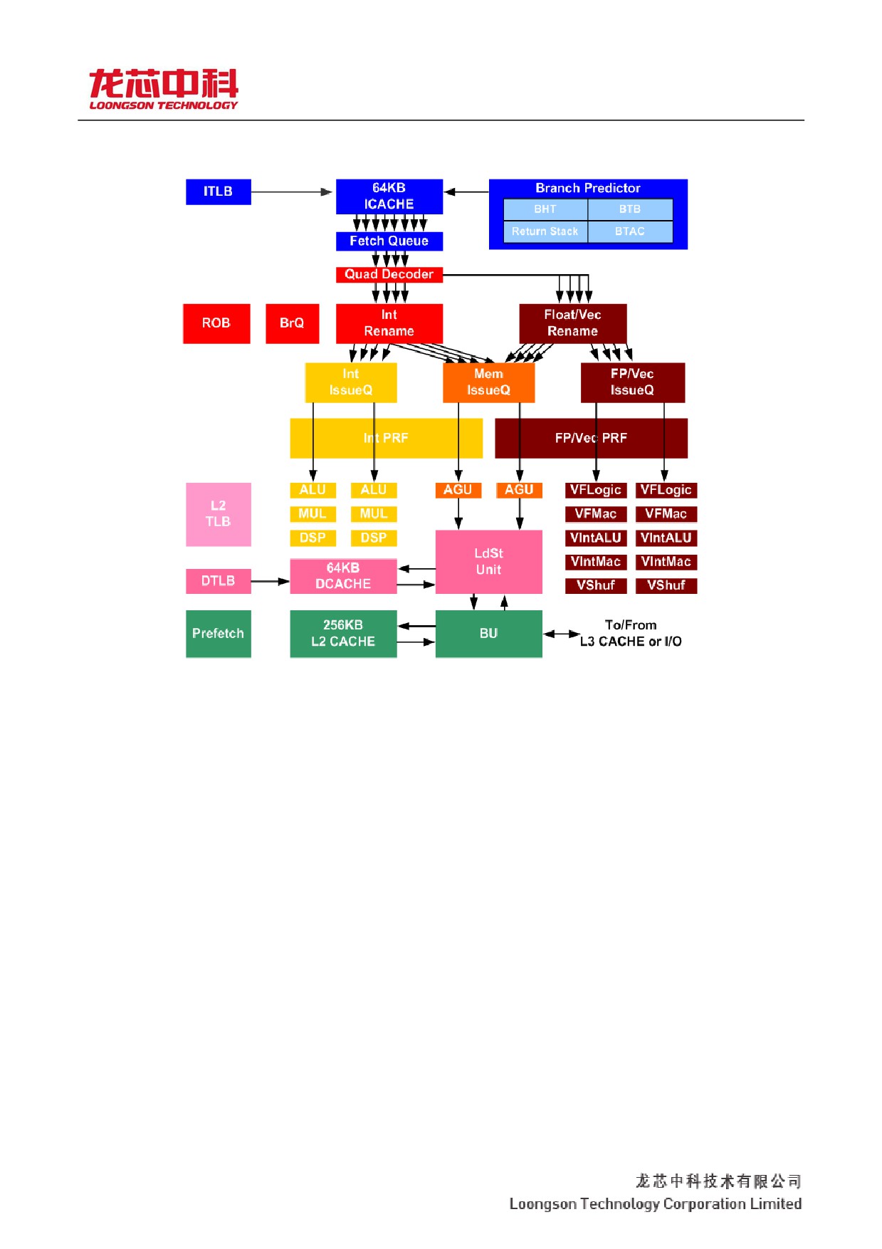
required in the execution stage. The basic structure of GS464E is shown in the figure below.
14
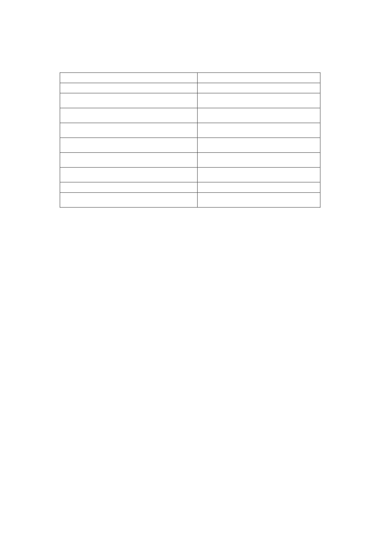
1.1 Speed overview of processor core structure parameters
Instruction set
MIPS64r2 compatible LoongISA instruction set
Flow depth
Grade 12
Take refers to the
8 instructions/cycles
width
Launch the width
(2 fixed point +2 floating point +2 access)/
period
Level 1 instruction
Private per core, 4 x 16KB/ channel
Cache specification
Level 1 data Cache
Private per core, 4 x 16KB/ channel
specification
Secondary Cache
Private per core, 16 channels ×16KB/ channel
specification
Three level Cache
Multi-core sharing, 16 channels ×128KB/
specifications
channel
TLB capacity
64 VTLB+2048 FTLB
TLB supports page
4KB (I =1, 2... i , 10)
sizes
龙芯 3A3000/3B3000 处理器用户手册 y 下册
2 Instruction set Overview
GS464E realized LoongISA v1.00 version of MIPS64 compatible basic part, MIPS64 DSP instruction
(MIPS64 DSP Module) and 64 common extension instruction (LoongEXT64).
2.1 MIPS64 compatible General instruction list
GS464E implements all of the MIPS64 specifications required to implement and a few optional
implementations of the generic instructions, its implementation of MIPS64 compatible generic instructions are
divided into the following categories by function:
y To fetch instruction
y Operation instruction
y Transfer instruction
y Other instructions
y Coprocessor 0 instruction
These instructions are listed class by class below.
2.1.1 To fetch instruction
MIPS architecture adopts load/ Store architecture. All operations are performed on registers, and only access
instructions can access the data in main memory. Access instruction includes read and write, unsigned read,
unaligned access and atomic access of various width data.
Table 2-1 CPU instruction set: access instruction
Instruction
Instruction
ISA
mnemonic
function
Compatible
description
Category
LB
In bytes
MIPS32
LBU
Takes an unsigned byte
MIPS32
LH
Take half word
MIPS32
LHU
Take the unsigned half word
MIPS32
LW
Take the word
MIPS32
LWU
Take the unsigned word
MIPS32
LWL
Take words left
MIPS32
LWR
Take the words right
MIPS32
LD
Take double word
MIPS64
LDL
Take the left part of the double word
MIPS64
LDR
Take the right part of the double word
MIPS64
LL
Take the address of the sign
MIPS32
LLD
Take the two-character address at the sign
MIPS64
SB
Remaining bytes
MIPS32
SH
Save half word
MIPS32
SW
characters
MIPS32
5
龙芯 3A3000/3B3000 处理器用户手册 y 下册
SWL
Characters left
MIPS32
SWR
To save words right
MIPS32
6
龙芯 3A3000/3B3000 处理器用户手册 y 下册
Instruction
Instruction
ISA
mnemonic
function
Compatible
description
Category
SD
Save double word
MIPS64
SDL
Save the left part of double characters
MIPS64
The SDR
Save the right part of double characters
MIPS64
SC
If I can save it
MIPS32
SCD
Meet the conditions to save double characters
MIPS64
2.1.2 Operation instruction
Operational instructions perform arithmetic, logic, shift, multiplication, and division operations on register
values. The operational instruction contains the register instruction format
(R-type, where the operands and
operation results are stored in the register) and the immediate instruction format (i-type, where one operand is a 16-
bit immediate number)
Table 2-2 Operation instruction: arithmetic instruction (ALU immediate number)
Instruction
Instruction
ISA
mnemonic
function
Compatible
description
Category
ADDI
Add number immediately
MIPS32
DADDI
Add double word number immediately
MIPS64
ADDIU
Add an unsigned immediate number
MIPS32
DADDIU
Add an unsigned double word number immediately
MIPS64
SLTI
Less than immediate Settings
MIPS32
SLTIU
Unsigned less than immediate number setting
MIPS32
ANDI
And immediately
MIPS32
ORI
Or the number immediately
MIPS32
XORI
Xor immediate number
MIPS32
LUI
Take immediate count to high
MIPS32
Table 2-3 Operation instruction: Arithmetic instruction (3 operands)
Instruction
Instruction
ISA
mnemonic
function
Compatible
description
Category
The ADD
add
MIPS32
DADD
Double word plus
MIPS64
ADDU
Unsigned add
MIPS32
DADDU
Unsigned double word plus
MIPS64
SUB
Reduction of
MIPS32
DSUB
Double word cut
MIPS64
SUBU
Unsigned reduction
MIPS32
DSUBU
Unsigned double word subtraction
MIPS64
SLT
Less than the set
MIPS32
SLTU
Unsigned less than set
MIPS32
The AND
with
MIPS32
7
龙芯 3A3000/3B3000 处理器用户手册 y 下册
The OR
or
MIPS32
XOR
Exclusive or
MIPS32
NOR
Or not
MIPS32
Table 2-4 Operation instruction: Arithmetic instruction (2 operands)
Instruction
Instruction
ISA
mnemonic
function
Compatible
description
Category
CLO
Word leading 1 number
MIPS32
DCLO
Double word leading 1 number
MIPS64
CLZ
The number of 0 word precursors
MIPS32
DCLZ
Double word leading 0 number
MIPS64
WSBH
Byte exchange in half word
MIPS32 R2
DSHD
Half-word exchange between words
MIPS64 R2
DSBH
Byte exchange in half word
MIPS64 R2
SEB
Byte symbol extension
MIPS32 R2
SEH
Half character extension
MIPS32 R2
INS
An insert
MIPS32 R2
EXT
An extract
MIPS32 R2
DINS
Double word bit insertion
MIPS64 R2
DINSM
Double word bit insertion
MIPS64 R2
DINSU
Double word bit insertion
MIPS64 R2
DEXT
Double word bit extraction
MIPS64 R2
DEXTM
Double word bit extraction
MIPS64 R2
DEXTU
Double word bit extraction
MIPS64 R2
Table 2-5 Operation instructions: multiplication and division instructions
Instruction
Instruction
ISA
mnemonic
function
Compatible
description
Category
The MUL
Multiply by the general register
MIPS32
MULT
take
MIPS32
DMULT
Double word by
MIPS64
MULTU
Unsigned by
MIPS32
DMULTU
Unsigned double word multiplication
MIPS64
MADD
By adding
MIPS32
MADDU
Unsigned multiplication plus
MIPS32
MSUB
By reducing
MIPS32
MSUBU
Unsigned times minus
MIPS32
DIV
In addition to
MIPS32
DDIV
Double word except
MIPS64
DIVU
Unsigned except
MIPS32
DDIVU
Unsigned double word division
MIPS64
MFHI
Take the number from the HI register to the general register
MIPS32
MTHI
From general purpose register to HI register
MIPS32
8
龙芯 3A3000/3B3000 处理器用户手册 y 下册
MFLO
Fetch from register LO to general purpose register
MIPS32
MTLO
From General Purpose register to LO register
MIPS32
Table 2-6 Operation instruction: shift instruction
Instruction
Instruction
ISA
mnemonic
function
Compatible
description
Category
SSL
The logical left
MIPS32
SRL
Logic moves to the right
MIPS32
SRA
Arithmetic moves to the right
MIPS32
SLLV
Variable logic moves left
MIPS32
SRLV
Variable logic moves to the right
MIPS32
SRAV
Variable arithmetic shift to the right
MIPS32
ROTR
Cycle moves to the right
MIPS32 R2
ROTRV
A variable loop moves to the right
MIPS32 R2
DSLL
Two-word logic moved left
MIPS64
DSRL
Two-word logic right shift
MIPS64
DSRA
Two-word arithmetic shift to the right
MIPS64
DSLLV
Variable two-word logic moves left
MIPS64
DSRLV
Variable two-word logic moves right
MIPS64
DSRAV
Variable two-word arithmetic shift to the right
MIPS64
DSLL32
Shift amount plus 32 double word logic to the left
MIPS64
DSRL32
Shift + 32 double word logic moves right
MIPS64
DSRA32
Shift amount plus 32 double word arithmetic shift to the right
MIPS64
DROTR
Double word loop right shift
MIPS64 R2
DROTR32
Shift amount plus 32 double word cycle right shift
MIPS64 R2
DROTRV
Double-word variable loop right shift
MIPS64 R2
2.1.3
Jump and branch instructions
Jump and branch instructions can change the control flow of a program, including the following four types:
y PC relative conditional branch
y PC unconditional jump
y Register absolute jump
y Procedure call
In MIPS architecture, all transfer instructions are followed by a delay slot instruction. Delay slots for Likely
transfer instructions are only executed when the transfer is successful; delay slots for non-likely transfer
instructions are always executed. The return address of a procedure call instruction is saved in register 31 by
default, and a jump based on register 31 is considered to be returned from the called procedure.
Table 2-7 Jump and branch instructions
Instruction
Instruction
ISA
mnemonic
function
Compatible
Category
description
9
龙芯 3A3000/3B3000 处理器用户手册 y 下册
J
jump
MIPS32
JAL
Call the procedure immediately
MIPS32
JR,
Jump to the instruction that the register points to
MIPS32
JR. HB
Jump to the instruction that the register points to
MIPS32 R2
JALR
Register call procedure
MIPS32
JALR. HB
Register call procedure
MIPS32 R2
BEQ
Equal jump
MIPS32
BNE
Unequal jump
MIPS32
10
龙芯 3A3000/3B3000 处理器用户手册 y 下册
Instruction
Instruction
ISA
mnemonic
function
Compatible
description
Category
BLEZ
Less than or equal to 0 jump
MIPS32
BGTZ
Jump greater than 0
MIPS32
BLTZ
Jump less than 0
MIPS32
BGEZ
A jump greater than or equal to 0
MIPS32
BLTZAL
Less than 0 calls the procedure
MIPS32
BGEZAL
Greater than or equal to 0 calls the procedure
MIPS32
BEQL
Equal is Likely to jump
MIPS32
BNEL
Not Likely to jump
MIPS32
BLEZL
Less than or equal to 0 is Likely to jump
MIPS32
BGTZL
Greater than 0 is Likely to jump
MIPS32
BLTZL
Less than 0 is Likely to jump
MIPS32
BGEZL
Greater than or equal to 0 is Likely to jump
MIPS32
BLTZALL
Less than 0 is Likely to call the procedure
MIPS32
BGEZALL
Greater than or equal to 0 is Likely to call the procedure
MIPS32
2.1.4 Coprocessor 0 instruction
The processor USES the Zero Coprocessor (CP0) register to manage memory and handle exceptions.
Table 2-8 Coprocessor 0 instructions
Instruction
Instruction
ISA
mnemonic
function
Compatible
description
Category
DMFC0
Take a double word from register CP0
MIPS64
DMTC0
Write double characters to register CP0
MIPS64
MFC0
Fetch the word from the CP0 register
MIPS32
MTC0
Write into register CP0
MIPS32
TLBR
Read the TLB entry of the index
MIPS32
TLBWI
Write the TLB entry for the index
MIPS32
TLBWR
Let me write the random TLB terms
MIPS32
TLBP
Search for matches in TLB
MIPS32
TLBINV
Invalid TLB table entry specified
MIPS32
TLBINVF
Invalid all TLB table entries
MIPS32
The CACHE
Cache operation
MIPS32
ERET
Abnormal return
MIPS32
DERET
Debug exception return
MIPS32
DMFGC0
Fetch a double word from the VIRTUAL machine REGISTER CP0
MIPS64
DMTGC0
Write double characters to the VIRTUAL machine CP0 register
MIPS64
MFGC0
Fetch from the VIRTUAL machine CP0 register
MIPS32
MTGC0
Write to the VIRTUAL machine CP0 register
MIPS32
DI 1
Disabling interrupts
MIPS32 R2
EI 2
Allow the interrupt
MIPS32 R2
11
龙芯 3A3000/3B3000 处理器用户手册 y 下册
Other instructions
In THE MIPS64, there are several other instructions in addition to those listed above.
Table 2-9 Other instructions: Special instructions
Instruction
Instruction
ISA
Compatible
mnemonic
function
Category
description
The SYSCALL
The system calls
MIPS32
BREAK
The breakpoint
MIPS32
HYPCALL
Virtual machine system call
MIPS32
The SYNC
synchronous
MIPS32
SYNCI
Synchronous instruction cache
MIPS32 R2
RDPGPR
Read shadow register
MIPS32
WRPGPR
Write shadow register
MIPS32
SDBBP
Debugging breakpoints
MIPS32
RDHWR
User mode reads machine state
MIPS32
WAIT
Waiting for instructions
MIPS32
Table 2-10 Other instructions: Exception trapped instruction
Instruction
Instruction
ISA
mnemonic
function
Compatible
description
Category
TGE
Greater than or equal to trapped
MIPS32
TGEU
The unsigned number is greater than or equal to trapped
MIPS32
TLT
Less than a
MIPS32
TLTU
The unsigned number is less than trapped
MIPS32
TEQ
Is equal to a
MIPS32
TNE
Differ in
MIPS32
TGEI
Greater than or equal to the immediate number trapped
MIPS32
TGEIU
Greater than or equal to unsigned immediate number trapped
MIPS32
TLTI
Less than immediate number trapped
MIPS32
TLTIU
Less than an unsigned immediate number is trapped
MIPS32
TEQI
Is equal to the number immediately trapped
MIPS32
TNEI
Does not equal to immediately number into
MIPS32
Table 2-11 Other instructions: conditional move instructions
Instruction
Instruction
ISA
mnemonic
function
Compatible
description
Category
MOVF
Condition moves when floating point condition is false
MIPS32
MOVT
The condition moves when the floating point condition is true
MIPS32
MOVN
Condition moves when the general register is not 0
MIPS32
MOVZ
The condition moves when the general register is 0
MIPS32
12
龙芯 3A3000/3B3000 处理器用户手册 y 下册
Table 2-12 Other instructions: Prefetch instructions
Instruction
Instruction
ISA
mnemonic
function
Compatible
description
Category
PREF
Prefetching instructions
MIPS32
13
龙芯 3A3000/3B3000 处理器用户手册 y 下册
Instruction
Instruction
ISA
mnemonic
function
Compatible
description
Category
PREFX
Prefetching instructions
MIPS32
2.2 MIPS64 is compatible with floating point instruction set overview
The floating-point instructions implemented in GS464E are compatible with the MIPS64 specification, and all
floating-point instructions are implemented in the Floting Point Unit (FPU). 1
2.2.1 FPU data type
The floating-point coprocessor supports both floating-point
and fixed-point data types.
Floating point data type
Floating-point data types supported by the floating-point coprocessor are:
y Single-precisions, S)
y Double-precisions, D)
y
64-bit Paired Single-Precisions (PS)
The floating-point coprocessor operates on single-precision floating-point Numbers (including pairs of single-
precision floating-point Numbers for each single precision number) and double-precision floating-point Numbers in
accordance with the ANSI/IEEE 754-1985 binary floating-point standards. The 32-bit single-precision format
includes a 24-bit decimal field (S+F) represented by a "symbol + amplitude" and an 8-bit exponential field (E); 64-
bit double format includes a 53-bit "symbol + amplitude"
Represents the decimal domain (S+F) and an 11-bit exponential domain (E); The 64-bit double precision (PS)
format contains two single-precision floating point formats.
The three types of data formats are shown in Figure 2-1.
Figure 2-1 FPU floating point data format
0
14
///////////////////////////////////////