Intel 64 and IA-32 Architectures. Software Developer’s Manual (Collection, 2023) - page 138
INSTRUCTION SET REFERENCE, A-Z
VPMADD52HUQ-Packed Multiply of Unsigned 52-Bit Integers and Add the High 52-Bit
Products to Qword Accumulators
Opcode/
Op/
64/32
CPUID Feature
Description
Instruction
En
bit Mode
Flag
Support
VEX.128.66.0F38.W1 B5 /r
A
V/V
AVX-IFMA
Multiply unsigned 52-bit integers in xmm2 and
xmm3/m128 and add the high 52 bits of the
VPMADD52HUQ xmm1, xmm2,
104-bit product to the qword unsigned
xmm3/m128
integers in xmm1.
VEX.256.66.0F38.W1 B5 /r
A
V/V
AVX-IFMA
Multiply unsigned 52-bit integers in ymm2 and
ymm3/m256 and add the high 52 bits of the
VPMADD52HUQ ymm1, ymm2,
104-bit product to the qword unsigned
ymm3/m256
integers in ymm1.
Instruction Operand Encoding
Op/En
Tuple
Operand 1
Operand 2
Operand 3
Operand 4
A
N/A
ModRM:reg (r, w)
VEX.vvvv (r)
ModRM:r/m (r)
N/A
Description
Multiplies packed unsigned 52-bit integers in each qword element of the first source operand (the second operand)
with the packed unsigned 52-bit integers in the corresponding elements of the second source operand (the third
operand) to form packed 104-bit intermediate results. The high 52-bit, unsigned integer of each 104-bit product is
added to the corresponding qword unsigned integer of the destination operand (the first operand).
Operation
VPMADDHUQ srcdest, src1, src2 (VEX version)
VL = (128,256)
KL = VL/64
FOR i in 0 .. KL-1:
temp128 := zeroextend64(src1.qword[i][51:0]) *zeroextend64(src2.qword[i][51:0])
srcdest.qword[i] := srcdest.qword[i] +zeroextend64(temp128[103:52])
srcdest[MAXVL:VL] := 0
SIMD Floating-Point Exceptions
None.
Other Exceptions
See Exceptions Type 4.
Document Number: 319433-050
2-51
INSTRUCTION SET REFERENCE, A-Z
VPMADD52LUQ-Packed Multiply of Unsigned 52-Bit Integers and Add the Low 52-Bit Products
to Qword Accumulators
Opcode/
Op/
64/32
CPUID Feature
Description
Instruction
En
bit Mode
Flag
Support
VEX.128.66.0F38.W1 B4 /r
A
V/V
AVX-IFMA
Multiply unsigned 52-bit integers in xmm2 and
xmm3/m128 and add the low 52 bits of the
VPMADD52LUQ xmm1, xmm2,
104-bit product to the qword unsigned
xmm3/m128
integers in xmm1.
VEX.256.66.0F38.W1 B4 /r
A
V/V
AVX-IFMA
Multiply unsigned 52-bit integers in ymm2 and
ymm3/m256 and add the low 52 bits of the
VPMADD52LUQ ymm1, ymm2,
104-bit product to the qword unsigned
ymm3/m256
integers in ymm1.
Instruction Operand Encoding
Op/En
Tuple
Operand 1
Operand 2
Operand 3
Operand 4
A
N/A
ModRM:reg (r, w)
VEX.vvvv (r)
ModRM:r/m (r)
N/A
Description
Multiplies packed unsigned 52-bit integers in each qword element of the first source operand (the second operand)
with the packed unsigned 52-bit integers in the corresponding elements of the second source operand (the third
operand) to form packed 104-bit intermediate results. The low 52-bit, unsigned integer of each 104-bit product is
added to the corresponding qword unsigned integer of the destination operand (the first operand).
Operation
VPMADDLUQ srcdest, src1, src2 (VEX version)
VL = (128,256)
KL = VL/64
FOR i in 0 .. KL-1:
temp128 := zeroextend64(src1.qword[i][51:0]) *zeroextend64(src2.qword[i][51:0])
srcdest.qword[i] := srcdest.qword[i] +zeroextend64(temp128[51:0])
srcdest[MAXVL:VL] := 0
SIMD Floating-Point Exceptions
None.
Other Exceptions
See Exceptions Type 4.
2-52
Document Number: 319433-050
INSTRUCTION SET REFERENCE, A-Z
VSHA512MSG1-Perform an Intermediate Calculation for the Next Four SHA512 Message
Qwords
Opcode/
Op/
64/32
CPUID Feature
Description
Instruction
En
bit Mode
Flag
Support
VEX.256.F2.0F38.W0 CC 11:rrr:bbb
A
V/V
AVX
Performs an intermediate calculation for the
next four SHA512 message qwords using
VSHA512MSG1 ymm1, xmm2
SHA512
previous message qwords from ymm1 and
xmm2, storing the result in ymm1.
Instruction Operand Encoding
Op/En
Tuple
Operand 1
Operand 2
Operand 3
Operand 4
A
N/A
ModRM:reg (r, w)
ModRM:r/m (r)
N/A
N/A
Description
The VSHA512MSG1 instruction is one of the two SHA512 message scheduling instructions. The instruction
performs an intermediate calculation for the next four SHA512 message qwords.
See https://nvlpubs.nist.gov/nistpubs/FIPS/NIST.FIPS.180-4.pdf for more information on the SHA512 standard.
Operation
define ROR64(qword, n):
count := n % 64
dest := (qword >> count) | (qword << (64-count))
return dest
define SHR64(qword, n):
return qword >> n
define s0(qword):
return ROR64(qword,1) ^ ROR64(qword, 8) ^ SHR64(qword, 7)
VSHA512MSG1 SRCDEST, SRC1
W[4] := SRC1.qword[0]
W[3] := SRCDEST.qword[3]
W[2] := SRCDEST.qword[2]
W[1] := SRCDEST.qword[1]
W[0] := SRCDEST.qword[0]
SRCDEST.qword[3] := W[3] + s0(W[4])
SRCDEST.qword[2] := W[2] + s0(W[3])
SRCDEST.qword[1] := W[1] + s0(W[2])
SRCDEST.qword[0] := W[0] + s0(W[1])
Flags Affected
None.
SIMD Floating-Point Exceptions
None.
Other Exceptions
See Exceptions Type 6.
Document Number: 319433-050
2-53
INSTRUCTION SET REFERENCE, A-Z
VSHA512MSG2-Perform a Final Calculation for the Next Four SHA512 Message Qwords
Opcode/
Op/
64/32
CPUID Feature
Description
Instruction
En
bit Mode
Flag
Support
VEX.256.F2.0F38.W0 CD 11:rrr:bbb
A
V/V
AVX
Performs the final calculation for the next four
SHA512 message qwords using previous
VSHA512MSG2 ymm1, ymm2
SHA512
message qwords from ymm1 and ymm2,
storing the result in ymm1.
Instruction Operand Encoding
Op/En
Tuple
Operand 1
Operand 2
Operand 3
Operand 4
A
N/A
ModRM:reg (r, w)
ModRM:r/m (r)
N/A
N/A
Description
The VSHA512MSG2 instruction is one of the two SHA512 message scheduling instructions. The instruction
performs the final calculation for the next four SHA512 message qwords.
See https://nvlpubs.nist.gov/nistpubs/FIPS/NIST.FIPS.180-4.pdf for more information on the SHA512 standard.
Operation
define ROR64(qword, n):
count := n % 64
dest := (qword >> count) | (qword << (64-count))
return dest
define SHR64(qword, n):
return qword >> n
define s1(qword):
return ROR64(qword,19) ^ ROR64(qword, 61) ^ SHR64(qword, 6)
VSHA512MSG2 SRCDEST, SRC1
W[14] := SRC1.qword[2]
W[15] := SRC1.qword[3]
W[16] := SRCDEST.qword[0] + s1(W[14])
W[17] := SRCDEST.qword[1] + s1(W[15])
W[18] := SRCDEST.qword[2] + s1(W[16])
W[19] := SRCDEST.qword[3] + s1(W[17])
SRCDEST.qword[3] := W[19]
SRCDEST.qword[2] := W[18]
SRCDEST.qword[1] := W[17]
SRCDEST.qword[0] := W[16]
Flags Affected
None.
SIMD Floating-Point Exceptions
None.
Other Exceptions
See Exceptions Type 6.
2-54
Document Number: 319433-050
INSTRUCTION SET REFERENCE, A-Z
VSHA512RNDS2-Perform Two Rounds of SHA512 Operation
Opcode/
Op/
64/32
CPUID Feature
Description
Instruction
En
bit Mode
Flag
Support
VEX.256.F2.0F38.W0 CB 11:rrr:bbb
A
V/V
AVX
Perform 2 rounds of SHA512 operation using
an initial SHA512 state (C,D,G,H) from ymm1,
VSHA512RNDS2 ymm1, ymm2,
SHA512
an initial SHA512 state (A,B,E,F) from ymm2,
xmm3
and a pre-computed sum of the next 2 round
message qwords and the corresponding round
constants from xmm3, storing the updated
SHA512 state (A,B,E,F) result in ymm1.
Instruction Operand Encoding
Op/En
Tuple
Operand 1
Operand 2
Operand 3
Operand 4
A
N/A
ModRM:reg (r, w)
VEX.vvvv (r)
ModRM:r/m (r)
N/A
Description
The VSHA512RNDS2 instruction performs two rounds of SHA512 operation using initial SHA512 state (C,D,G,H)
from the first operand, an initial SHA512 state (A,B,E,F) from the second operand, and a pre-computed sum of the
next two round message qwords and the corresponding round constants from the third operand (only the two
lower qwords of the third operand). The updated SHA512 state (A,B,E,F) is written to the first operand, and the
second operand can be used as the updated state (C,D,G,H) in later rounds.
See https://nvlpubs.nist.gov/nistpubs/FIPS/NIST.FIPS.180-4.pdf for more information on the SHA512 standard.
Operation
define ROR64(qword, n):
count := n % 64
dest := (qword >> count) | (qword << (64-count))
return dest
define SHR64(qword, n):
return qword >> n
define cap_sigma0(qword):
return ROR64(qword,28) ^ ROR64(qword, 34) ^ ROR64(qword, 39)
define cap_sigma1(qword):
return ROR64(qword,14) ^ ROR64(qword, 18) ^ ROR64(qword, 41)
define MAJ(a,b,c):
return (a & b) ^ (a & c) ^ (b & c)
define CH(e,f,g):
return (e & f) ^ (g & ~e)
Document Number: 319433-050
2-55
INSTRUCTION SET REFERENCE, A-Z
VSHA512RNDS2 SRCDEST, SRC1, SRC2
A[0] := SRC1.qword[3]
B[0] := SRC1.qword[2]
C[0] := SRCDEST.qword[3]
D[0] := SRCDEST.qword[2]
E[0] := SRC1.qword[1]
F[0] := SRC1.qword[0]
G[0] := SRCDEST.qword[1]
H[0] := SRCDEST.qword[0]
WK[0]:= SRC2.qword[0]
WK[1]:= SRC2.qword[1]
FOR i in 0..1:
A[i+1] := CH(E[i], F[i], G[i]) +
cap_sigma1(E[i]) + WK[i] + H[i] +
MAJ(A[i], B[i], C[i]) +
cap_sigma0(A[i])
B[i+1] := A[i]
C[i+1] := B[i]
D[i+1] := C[i]
E[i+1] := CH(E[i], F[i], G[i]) +
cap_sigma1(E[i]) + WK[i] + H[i] + D[i]
F[i+1] := E[i]
G[i+1] := F[i]
H[i+1] := G[i]
SRCDEST.qword[3] = A[2]
SRCDEST.qword[2] = B[2]
SRCDEST.qword[1] = E[2]
SRCDEST.qword[0] = F[2]
Flags Affected
None.
SIMD Floating-Point Exceptions
None.
Other Exceptions
See Exceptions Type 6.
2-56
Document Number: 319433-050
INSTRUCTION SET REFERENCE, A-Z
VSM3MSG1-Perform Initial Calculation for the Next Four SM3 Message Words
Opcode/
Op/
64/32
CPUID Feature
Description
Instruction
En
bit Mode
Flag
Support
VEX.128.NP.0F38.W0 DA /r
A
V/V
AVX
Performs an initial calculation for the next four
SM3 message words using previous message
VSM3MSG1 xmm1, xmm2,
SM3
words from xmm2 and xmm3/m128, storing
xmm3/m128
the result in xmm1.
Instruction Operand Encoding
Op/En
Tuple
Operand 1
Operand 2
Operand 3
Operand 4
A
N/A
ModRM:reg (r, w)
VEX.vvvv (r)
ModRM:r/m (r)
N/A
Description
The VSM3MSG1 instruction is one of the two SM3 message scheduling instructions. The instruction performs an
initial calculation for the next four SM3 message words.
Operation
define ROL32(dword, n):
count := n % 32
dest := (dword << count) | (dword >> (32-count))
return dest
define P1(x):
return x ^ ROL32(x, 15) ^ ROL32(x, 23)
VSM3MSG1 SRCDEST, SRC1, SRC2
W[0] := SRC2.dword[0]
W[1] := SRC2.dword[1]
W[2] := SRC2.dword[2]
W[3] := SRC2.dword[3]
W[7] := SRCDEST.dword[0]
W[8] := SRCDEST.dword[1]
W[9] := SRCDEST.dword[2]
W[10] := SRCDEST.dword[3]
W[13] := SRC1.dword[0]
W[14] := SRC1.dword[1]
W[15] := SRC1.dword[2]
TMP0 := W[7] ^ W[0] ^ ROL32(W[13], 15)
TMP1 := W[8] ^ W[1] ^ ROL32(W[14], 15)
TMP2 := W[9] ^ W[2] ^ ROL32(W[15], 15)
TMP3 := W[10] ^ W[3]
SRCDEST.dword[0] := P1(TMP0)
SRCDEST.dword[1] := P1(TMP1)
SRCDEST.dword[2] := P1(TMP2)
SRCDEST.dword[3] := P1(TMP3)
Document Number: 319433-050
2-57
INSTRUCTION SET REFERENCE, A-Z
Flags Affected
None.
SIMD Floating-Point Exceptions
None.
Other Exceptions
See Exceptions Type 4.
2-58
Document Number: 319433-050
INSTRUCTION SET REFERENCE, A-Z
VSM3MSG2-Perform Final Calculation for the Next Four SM3 Message Words
Opcode/
Op/
64/32
CPUID Feature
Description
Instruction
En
bit Mode
Flag
Support
VEX.128.66.0F38.W0 DA /r
A
V/V
AVX
Performs the final calculation for the next four
SM3 message words using previous message
VSM3MSG2 xmm1, xmm2,
SM3
words from xmm2 and xmm3/m128, storing
xmm3/m128
the result in xmm1.
Instruction Operand Encoding
Op/En
Tuple
Operand 1
Operand 2
Operand 3
Operand 4
A
N/A
ModRM:reg (r, w)
VEX.vvvv (r)
ModRM:r/m (r)
N/A
Description
The VSM3MSG2 instruction is one of the two SM3 message scheduling instructions. The instruction performs the
final calculation for the next four SM3 message words.
Operation
//see the VSM3MSG1 instruction for definition of ROL32()
VSM3MSG2 SRCDEST, SRC1, SRC2
WTMP[0] := SRCDEST.dword[0]
WTMP[1] := SRCDEST.dword[1]
WTMP[2] := SRCDEST.dword[2]
WTMP[3] := SRCDEST.dword[3]
// Dword array W[] has indices are based on the SM3 specification.
W[3] := SRC1.dword[0]
W[4] := SRC1.dword[1]
W[5] := SRC1.dword[2]
W[6] := SRC1.dword[3]
W[10] := SRC2.dword[0]
W[11] := SRC2.dword[1]
W[12] := SRC2.dword[2]
W[13] := SRC2.dword[3]
W[16] := ROL32(W[3], 7) ^ W[10] ^ WTMP[0]
W[17] := ROL32(W[4], 7) ^ W[11] ^ WTMP[1]
W[18] := ROL32(W[5], 7) ^ W[12] ^ WTMP[2]
W[19] := ROL32(W[6], 7) ^ W[13] ^ WTMP[3]
W[19] := W[19] ^ ROL32(W[16], 6) ^ ROL32(W[16], 15) ^ ROL32(W[16], 30)
SRCDEST.dword[0] := W[16]
SRCDEST.dword[1] := W[17]
SRCDEST.dword[2] := W[18]
SRCDEST.dword[3] := W[19]
Flags Affected
None.
Document Number: 319433-050
2-59
INSTRUCTION SET REFERENCE, A-Z
SIMD Floating-Point Exceptions
None.
Other Exceptions
See Exceptions Type 4.
2-60
Document Number: 319433-050
INSTRUCTION SET REFERENCE, A-Z
VSM3RNDS2-Perform Two Rounds of SM3 Operation
Opcode/
Op/
64/32
CPUID Feature
Description
Instruction
En
bit Mode
Flag
Support
VEX.128.66.0F3A.W0 DE /r /ib
A
V/V
AVX
Performs two rounds of SM3 operation using
the initial SM3 states from xmm1 and xmm2,
VSM3RNDS2 xmm1, xmm2,
SM3
and pre-computed words from xmm3/m128,
xmm3/m128, imm8
storing the result in xmm1.
Instruction Operand Encoding
Op/En
Tuple
Operand 1
Operand 2
Operand 3
Operand 4
A
N/A
ModRM:reg (r, w)
VEX.vvvv (r)
ModRM:r/m (r)
imm8
Description
The VSM3RNDS2 instruction performs two rounds of SM3 operation using initial SM3 state (C, D, G, H) from the
first operand, an initial SM3 states (A, B, E, F) from the second operand and a pre-computed words from the third
operand. The first operand with initial SM3 state of (C, D, G, H) assumes input of non-rotated left variables from
previous state. The updated SM3 state (A, B, E, F) is written to the first operand.
The imm8 should contain the even round number for the first of the two rounds computed by this instruction. The
computation masks the imm8 value by AND’ing it with 0x3E so that only even round numbers from 0 through 62
are used for this operation.
Operation
//see the VSM3MSG1 instruction for definition of ROL32()
define P0(dword):
return dword ^ ROL32(dword, 9) ^ ROL32(dword, 17)
define FF(x,y,z, round):
if round < 16:
return (x ^ y ^ z)
else:
return (x & y) | (x & z) | (y & z)
define GG(x,y,z, round):
if round < 16:
return (x ^ y ^ z)
else:
return (x & y) | (~x & z)
VSM3RNDS2 SRCDEST, SRC1, SRC2, IMM8
A[0] := SRC1.dword[3]
B[0] := SRC1.dword[2]
C[0] := SRCDEST.dword[3]
D[0] := SRCDEST.dword[2]
E[0] := SRC1.dword[1]
F[0] := SRC1.dword[0]
G[0] := SRCDEST.dword[1]
H[0] := SRCDEST.dword[0]
W[0] := SRC2.dword[0]
W[1] := SRC2.dword[1]
W[4] := SRC2.dword[2]
Document Number: 319433-050
2-61
INSTRUCTION SET REFERENCE, A-Z
W[5] := SRC2.dword[3]
C[0] := ROL32(C[0], 9)
D[0] := ROL32(D[0], 9)
G[0] := ROL32(G[0], 19)
H[0] := ROL32(H[0], 19)
ROUND := IMM8 & 0x3E // even numbers 0...62
IF ROUND < 16:
CONST := 0x79cc4519
ELSE:
CONST := 0x7a879d8a
CONST := ROL32(CONST,ROUND)
FOR i in 0..1:
S1 := ROL32((ROL32(A[i], 12) + E[i] + CONST), 7)
S2 := S1 ^ ROL32(A[i],12)
T1 := FF(A[i], B[i], C[i], ROUND) + D[i] + S2 + (W[i]^W[i+4])
T2 := GG(E[i], F[i], G[i], ROUND) + H[i] + S1 + W[i]
D[i+1] := C[i]
C[i+1] := ROL32(B[i],9)
B[i+1] := A[i]
A[i+1] := T1
H[i+1] := G[i]
G[i+1] := ROL32(F[i], 19)
F[i+1] := E[i]
E[i+1] := P0(T2)
CONST := ROL32(CONST, 1)
SRCDEST.dword[3] := A[2]
SRCDEST.dword[2] := B[2]
SRCDEST.dword[1] := E[2]
SRCDEST.dword[0] := F[2]
Flags Affected
None.
SIMD Floating-Point Exceptions
None.
Other Exceptions
See Exceptions Type 4.
2-62
Document Number: 319433-050
INSTRUCTION SET REFERENCE, A-Z
VSM4KEY4-Perform Four Rounds of SM4 Key Expansion
Opcode/
Op/
64/32
CPUID Feature
Description
Instruction
En
bit Mode
Flag
Support
VEX.128.F3.0F38.W0 DA /r
A
V/V
AVX
Performs four rounds of SM4 key expansion.
VSM4KEY4 xmm1, xmm2,
SM4
xmm3/m128
VEX.256.F3.0F38.W0 DA /r
A
V/V
AVX
Performs four rounds of SM4 key expansion.
VSM4KEY4 ymm1, ymm2,
SM4
ymm3/m256
Instruction Operand Encoding
Op/En
Tuple
Operand 1
Operand 2
Operand 3
Operand 4
A
N/A
ModRM:reg (w)
VEX.vvvv (r)
ModRM:r/m (r)
N/A
Description
The VSM4KEY4 instruction performs four rounds of SM4 key expansion. The instruction operates on independent
128-bit lanes.
Additional details can be found at: https://tools.ietf.org/html/draft-ribose-cfrg-sm4-10.
Both SM4 instructions use a common sbox table:
BYTE sbox[256] = {
0xD6, 0x90, 0xE9, 0xFE, 0xCC, 0xE1, 0x3D, 0xB7, 0x16, 0xB6, 0x14, 0xC2, 0x28, 0xFB, 0x2C, 0x05,
0x2B, 0x67, 0x9A, 0x76, 0x2A, 0xBE, 0x04, 0xC3, 0xAA, 0x44, 0x13, 0x26, 0x49, 0x86, 0x06, 0x99,
0x9C, 0x42, 0x50, 0xF4, 0x91, 0xEF, 0x98, 0x7A, 0x33, 0x54, 0x0B, 0x43, 0xED, 0xCF, 0xAC, 0x62,
0xE4, 0xB3, 0x1C, 0xA9, 0xC9, 0x08, 0xE8, 0x95, 0x80, 0xDF, 0x94, 0xFA, 0x75, 0x8F, 0x3F, 0xA6,
0x47, 0x07, 0xA7, 0xFC, 0xF3, 0x73, 0x17, 0xBA, 0x83, 0x59, 0x3C, 0x19, 0xE6, 0x85, 0x4F, 0xA8,
0x68, 0x6B, 0x81, 0xB2, 0x71, 0x64, 0xDA, 0x8B, 0xF8, 0xEB, 0x0F, 0x4B, 0x70, 0x56, 0x9D, 0x35,
0x1E, 0x24, 0x0E, 0x5E, 0x63, 0x58, 0xD1, 0xA2, 0x25, 0x22, 0x7C, 0x3B, 0x01, 0x21, 0x78, 0x87,
0xD4, 0x00, 0x46, 0x57, 0x9F, 0xD3, 0x27, 0x52, 0x4C, 0x36, 0x02, 0xE7, 0xA0, 0xC4, 0xC8, 0x9E,
0xEA, 0xBF, 0x8A, 0xD2, 0x40, 0xC7, 0x38, 0xB5, 0xA3, 0xF7, 0xF2, 0xCE, 0xF9, 0x61, 0x15, 0xA1,
0xE0, 0xAE, 0x5D, 0xA4, 0x9B, 0x34, 0x1A, 0x55, 0xAD, 0x93, 0x32, 0x30, 0xF5, 0x8C, 0xB1, 0xE3,
0x1D, 0xF6, 0xE2, 0x2E, 0x82, 0x66, 0xCA, 0x60, 0xC0, 0x29, 0x23, 0xAB, 0x0D, 0x53, 0x4E, 0x6F,
0xD5, 0xDB, 0x37, 0x45, 0xDE, 0xFD, 0x8E, 0x2F, 0x03, 0xFF, 0x6A, 0x72, 0x6D, 0x6C, 0x5B, 0x51,
0x8D, 0x1B, 0xAF, 0x92, 0xBB, 0xDD, 0xBC, 0x7F, 0x11, 0xD9, 0x5C, 0x41, 0x1F, 0x10, 0x5A, 0xD8,
0x0A, 0xC1, 0x31, 0x88, 0xA5, 0xCD, 0x7B, 0xBD, 0x2D, 0x74, 0xD0, 0x12, 0xB8, 0xE5, 0xB4, 0xB0,
0x89, 0x69, 0x97, 0x4A, 0x0C, 0x96, 0x77, 0x7E, 0x65, 0xB9, 0xF1, 0x09, 0xC5, 0x6E, 0xC6, 0x84,
0x18, 0xF0, 0x7D, 0xEC, 0x3A, 0xDC, 0x4D, 0x20, 0x79, 0xEE, 0x5F, 0x3E, 0xD7, 0xCB, 0x39, 0x48
}
Operation
define ROL32(dword, n):
count := n % 32
dest := (dword << count) | (dword >> (32-count))
return dest
define SBOX_BYTE(dword, i):
// sbox[] array defined in introduction
return sbox[dword.byte[i]]
define lower_t(dword):
tmp.byte[0] := SBOX_BYTE(dword, 0)
Document Number: 319433-050
2-63
INSTRUCTION SET REFERENCE, A-Z
tmp.byte[1] := SBOX_BYTE(dword, 1)
tmp.byte[2] := SBOX_BYTE(dword, 2)
tmp.byte[3] := SBOX_BYTE(dword, 3)
return tmp
define L_KEY(dword):
return dword ^ ROL32(dword, 13) ^ ROL32(dword, 23)
define T_KEY(dword):
return L_KEY(lower_t(dword))
define F_KEY(X0, X1, X2, X3, round_key):
return X0 ^ T_KEY(X1 ^ X2 ^ X3 ^ round_key)
VSM4KEY4 DEST, SRC1, SRC2
VL = (128, 256)
KL := VL/128
for i in 0..KL-1:
P[0] := SRC1.xmm[i].dword[0]
P[1] := SRC1.xmm[i].dword[1]
P[2] := SRC1.xmm[i].dword[2]
P[3] := SRC1.xmm[i].dword[3]
C[0] := F_KEY(P[0], P[1], P[2], P[3], SRC2.xmm[i].dword[0])
C[1] := F_KEY(P[1], P[2], P[3], C[0], SRC2.xmm[i].dword[1])
C[2] := F_KEY(P[2], P[3], C[0], C[1], SRC2.xmm[i].dword[2])
C[3] := F_KEY(P[3], C[0], C[1], C[2], SRC2.xmm[i].dword[3])
DEST.xmm[i].dword[0] := C[0]
DEST.xmm[i].dword[1] := C[1]
DEST.xmm[i].dword[2] := C[2]
DEST.xmm[i].dword[3] := C[3]
DEST[MAXVL-1:VL] := 0
Flags Affected
None.
SIMD Floating-Point Exceptions
None.
Other Exceptions
See Exceptions Type 6.
2-64
Document Number: 319433-050
INSTRUCTION SET REFERENCE, A-Z
VSM4RNDS4-Performs Four Rounds of SM4 Encryption
Opcode/
Op/
64/32
CPUID Feature
Description
Instruction
En
bit Mode
Flag
Support
VEX.128.F2.0F38.W0 DA /r
A
V/V
AVX
Performs four rounds of SM4 encryption.
VSM4RNDS4 xmm1, xmm2,
SM4
xmm3/m128
VEX.256.F2.0F38.W0 DA /r
A
V/V
AVX
Performs four rounds of SM4 encryption.
VSM4RNDS4 ymm1, ymm2,
SM4
ymm3/m256
Instruction Operand Encoding
Op/En
Tuple
Operand 1
Operand 2
Operand 3
Operand 4
A
N/A
ModRM:reg (w)
VEX.vvvv (r)
ModRM:r/m (r)
N/A
Description
The SM4RNDS4 instruction performs four rounds of SM4 encryption. The instruction operates on independent 128-
bit lanes.
Additional details can be found at: https://tools.ietf.org/html/draft-ribose-cfrg-sm4-10.
See “VSM4KEY4-Perform Four Rounds of SM4 Key Expansion” for the sbox table.
Operation
// see the VSM4KEY4 instruction for the definition of ROL32, lower_t
define L_RND(dword):
tmp := dword
tmp := tmp ^ ROL32(dword, 2)
tmp := tmp ^ ROL32(dword, 10)
tmp := tmp ^ ROL32(dword, 18)
tmp := tmp ^ ROL32(dword, 24)
return tmp
define T_RND(dword):
return L_RND(lower_t(dword))
define F_RND(X0, X1, X2, X3, round_key):
return X0 ^ T_RND(X1 ^ X2 ^ X3 ^ round_key)
Document Number: 319433-050
2-65
INSTRUCTION SET REFERENCE, A-Z
VSM4RNDS4 DEST, SRC1, SRC2
VL = (128,256)
KL := VL/128
for i in 0..KL-1:
P[0] := SRC1.xmm[i].dword[0]
P[1] := SRC1.xmm[i].dword[1]
P[2] := SRC1.xmm[i].dword[2]
P[3] := SRC1.xmm[i].dword[3]
C[0] := F_RND(P[0], P[1], P[2], P[3], SRC2.xmm[i].dword[0])
C[1] := F_RND(P[1], P[2], P[3], C[0], SRC2.xmm[i].dword[1])
C[2] := F_RND(P[2], P[3], C[0], C[1], SRC2.xmm[i].dword[2])
C[3] := F_RND(P[3], C[0], C[1], C[2], SRC2.xmm[i].dword[3])
DEST.xmm[i].dword[0] := C[0]
DEST.xmm[i].dword[1] := C[1]
DEST.xmm[i].dword[2] := C[2]
DEST.xmm[i].dword[3] := C[3]
DEST[MAXVL-1:VL] := 0
Flags Affected
None.
SIMD Floating-Point Exceptions
None.
Other Exceptions
See Exceptions Type 6.
2-66
Document Number: 319433-050
INSTRUCTION SET REFERENCE, A-Z
WRMSRLIST-Write List of Model Specific Registers
Opcode /
Op/
64/32 bit
CPUID Feature Flag
Description
Instruction
En
Mode
Support
F3 0F 01 C6
ZO
V/N.E.
MSRLIST
Write requested list of MSRs with the values
specified in memory.
WRMSRLIST
Instruction Operand Encoding
Op/En
Operand 1
Operand 2
Operand 3
Operand 4
ZO
N/A
N/A
N/A
N/A
Description
This instruction writes a software-provided list of up to 64 MSRs with values loaded from memory.
WRMSRLIST takes three implied input operands:
• RSI: Linear address of a table of MSR addresses (8 bytes per address)1.
• RDI: Linear address of a table from which MSR data is loaded (8 bytes per MSR).
• RCX: 64-bit bitmask of valid bits for the MSRs. Bit 0 is the valid bit for entry 0 in each table, etc.
For each RCX bit [n] from 0 to 63, if RCX[n] is 1, WRMSRLIST will write the MSR specified at entry [n] in the RSI
table with the value read from memory at the entry [n] in the RDI table.
This implies a maximum of 64 MSRs that can be processed by this instruction. The processor will clear RCX[n] after
it finishes handling that MSR. Similar to repeated string operations, WRMSRLIST supports partial completion for
interrupts, exceptions, and traps. In these situations, the RIP register saved will point to the MSRLIST instruction
while the RCX register will have cleared bits corresponding to all completed iterations.
This instruction must be executed at privilege level 0; otherwise, a general protection exception #GP(0) is gener-
ated. This instruction performs MSR specific checks and respects the VMX MSR VM-execution controls in the same
manner as WRMSR.
Like WRMSRNS (and unlike WRMSR), WRMSRLIST is not defined as a serializing instruction (see “Serializing
Instructions” in Chapter 9 of the Intel® 64 and IA-32 Architectures Software Developer’s Manual, Volume 3A). This
means that software should not rely on WRMSRLIST to drain all buffered writes to memory before the next instruc-
tion is fetched and executed. For implementation reasons, some processors may serialize when writing certain
MSRs, even though that is not guaranteed.
Like WRMSR and WRMSRNS, WRMSRLIST will ensure that all operations before the WRMSRLIST do not use the new
MSR value and that all operations after the WRMSRLIST do use the new value. An exception to this rule is certain
store-related performance monitor events that only count when those stores are drained to memory. Since
WRMSRLIST is not a serializing instruction, if software is using WRMSRLIST to change the controls for such perfor-
mance monitor events, then stores before the WRMSRLIST may be counted with new MSR values written by
WRMSRLIST. Software can insert the SERIALIZE instruction before the WRMSRLIST if so desired.
Those MSRs that cause a TLB invalidation when they are written via WRMSR (e.g., MTRRs) will also cause the same
TLB invalidation when written by WRMSRLIST.
In places where WRMSR is being used as a proxy for a serializing instruction, a different serializing instruction can
be used (e.g., SERIALIZE).
WRMSRLIST writes MSRs in order, which means the processor will ensure that an MSR in iteration “n” will be
written only after previous iterations (“n-1”). If the older MSR writes had a side effect that affects the behavior of
the next MSR, the processor will ensure that side effect is honored.
The processor is allowed to (but not required to) “load ahead” in the list. Examples:
• Use old memory type or TLB translation for loads from list memory despite an MSR written by a previous
iteration changing MTRR or invalidating TLBs.
1. Since MSR addresses are only 32-bits wide, bits 63:32 of each MSR address table entry is reserved.
Document Number: 319433-050
2-67
INSTRUCTION SET REFERENCE, A-Z
• Cause a page fault or EPT violation for a memory access to an entry > “n” in MSR address or data tables,
despite the processor only having read or written “n” MSRs.1
Virtualization Behavior-VM Exit Causes
Like WRMSR, the WRMSRLIST instruction executed in VMX non-root operation causes a VM exit if any of the
following are true:
• The “use MSR bitmaps” VM-execution control is 0.
• The value of MSR address is not in the ranges 00000000H-00001FFFH and C0000000H-C0001FFFH.
• The value of MSR address is in the range 00000000H-00001FFFH and bit n in read bitmap for low MSRs is 1,
where n is the value of the MSR address.
• The value of MSR address is in the range C0000000H-C0001FFFH and bit n in read bitmap for high MSRs is 1,
where n is the value of the MSR address & 00001FFFH.
A VM exit for the above reasons for the WRMSRLIST instruction will specify exit reason 79 (decimal). The exit qual-
ification is set to the MSR address causing the VM exit if the “use MSR bitmaps” VM-execution control is 1. If the
“use MSR bitmaps” VM-execution control is 0, then the VM-exit qualification will be 0.
VM exits due to attempts to write, with WRMSRLIST, an MSR that is blocked by the MSR bitmaps will provide in a
new VMCS field (called “MSR data”) the 64-bit data that WRMSRLIST would have written to the MSR had the VM
exit not occurred. This field is undefined for VM exits that do not define it. The encoding for this field is
2402H/2403H.
Software handling a VM exit by WRMSRLIST can emulate a single iteration of the instruction using the MSR index
in the exit qualification and the data provided in the new “MSR data” VMCS field.
Virtualization Behavior-Changed Behavior in Non-Root Operation
The previous section identifies when executions of the WRMSRLIST instruction cause VM exits. Under the following
situations, a #UD will occur instead of a VM exit or a fault due to CPL 0:
• The “enable MSR-list instructions” VM-execution control (tertiary processor-based VM-execution control 6) is 0.
• The “Activate tertiary controls” VM-execution control is 0.
If that does not occur and there is no fault due to CPL > 0 nor a VM exit, the instruction’s behavior may be modified
for certain values of MSR address in the same manner as WRMSR for a read of the same MSR.
Operation
DO WHILE RCX != 0
MSR_index := position of least significant bit set in RCX;
Load MSR_address_table_entry from 8 bytes at the linear address RSI + (MSR_index * 8);
Load MSR_data from 8 bytes at the linear address RDI + (MSR_index * 8);
IF MSR_address_table_entry[63:32] != 0 THEN #GP(0); FI;
MSR_address := MSR_address_table_entry[31:0];
IF WRMSR of MSR_data to the MSR with address MSR_address would #GP THEN #GP(0); FI;
Load the MSR with address MSR_address with MSR_data;
RCX[MSR_index] := 0;
Allow delivery of any pending interrupts or traps;
OD;
Flags Affected
None.
Protected Mode Exceptions
#UD
The WRMSRLIST instruction is not recognized in protected mode.
1. For example, the processor may take a page fault due to a linear address for the 10th entry in the MSR address table despite only
having completed the MSR writes up to entry 5.
2-68
Document Number: 319433-050
INSTRUCTION SET REFERENCE, A-Z
Real-Address Mode Exceptions
#UD
The WRMSRLIST instruction is not recognized in real-address mode.
Virtual-8086 Mode Exceptions
#UD
The WRMSRLIST instruction is not recognized in virtual-8086 mode.
Compatibility Mode Exceptions
#UD
The WRMSRLIST instruction is not recognized in compatibility mode.
64-Bit Mode Exceptions
#GP(0)
If the current privilege level is not 0.
If RSI [2:0] ≠ 0, RDI [2:0] ≠ 0, or bits 63:32 of an MSR-address table entry are not all zero.
If an execution of WRMSR to a specified MSR with a specified value would generate a general-
protection exception (#GP(0)).
#UD
If the LOCK prefix is used.
If not in 64-bit mode.
If CPUID.(EAX=07H, ECX=01H):EAX.MSRLIST[bit 27] = 0.
Document Number: 319433-050
2-69
INSTRUCTION SET REFERENCE, A-Z
WRMSRNS-Non-Serializing Write to Model Specific Register
Opcode/
Op/
64/32 Bit
CPUID Feature
Description
Instruction
En
Mode
Flag
Support
NP 0F 01 C6
ZO
V/V
WRMSRNS
Write the value in EDX:EAX to MSR specified by
ECX.
WRMSRNS
Instruction Operand Encoding
Op/En
Operand 1
Operand 2
Operand 3
Operand 4
ZO
N/A
N/A
N/A
N/A
Description
WRMSRNS is an instruction that behaves exactly like WRMSR, with the only difference being that it is not a serial-
izing instruction by default.
Writes the contents of registers EDX:EAX into the 64-bit model specific register (MSR) specified in the ECX register.
The contents of the EDX register are copied to the high-order 32 bits of the selected MSR and the contents of the
EAX register are copied to the low-order 32 bits of the MSR. The high-order 32 bits of RAX, RCX, and RDX are
ignored.
This instruction must be executed at privilege level 0 or in real-address mode; otherwise, a general protection
exception #GP(0) is generated.
Unlike WRMSR, WRMSRNS is not defined as a serializing instruction (see “Serializing Instructions” in Chapter 9 of
the Intel® 64 and IA-32 Architectures Software Developer’s Manual, Volume 3A). This means that software should
not rely on it to drain all buffered writes to memory before the next instruction is fetched and executed. For imple-
mentation reasons, some processors may serialize when writing certain MSRs, even though that is not guaranteed.
Like WRMSR, WRMSRNS will ensure that all operations before it do not use the new MSR value and that all opera-
tions after the WRMSRNS do use the new value. An exception to this rule is certain store related performance
monitor events that only count when those stores are drained to memory. Since WRMSRNS is not a serializing
instruction, if software is using WRMSRNS to change the controls for such performance monitor events, then stores
before the WRMSRMS may be counted with new MSR values written by WRMSRNS. Software can insert the SERI-
ALIZE instruction before the WRMSRNS if so desired.
Those MSRs that cause a TLB invalidation when they are written via WRMSR (e.g., MTRRs) will also cause the same
TLB invalidation when written by WRMSRNS.
In order to improve performance, software may replace WRMSR with WRMSRNS. In places where WRMSR is being
used as a proxy for a serializing instruction, a different serializing instruction can be used (e.g., SERIALIZE).
Operation
MSR[ECX] := EDX:EAX;
Flags Affected
None.
Exceptions
Same exceptions as WRMSR.
#UD
If CPUID.(EAX=07H, ECX=01H):EAX.WRMSRNS[bit 19] = 0.
2-70
Document Number: 319433-050
INTEL® AMX INSTRUCTION SET REFERENCE, A-Z
CHAPTER 3
INTEL® AMX INSTRUCTION SET REFERENCE, A-Z
NOTES
The following Intel® AMX instructions have moved to the Intel® 64 and IA-32 Architectures
Software Developer’s Manual: LDTILECFG, STTILECFG, TDPBF16PS,
TDPBSSD/TDPBSUD/TDPBUSD/TDPBUUD, TILELOADD/TILELOADDT1, TILERELEASE,
TILESTORED, and TILEZERO.
The Intel Advanced Matrix Extensions introductory material and helper functions will be maintained
here, as well as in the Intel® 64 and IA-32 Architectures Software Developer’s Manual, for the
reader’s convenience. For information on Intel AMX and the XSAVE feature set, and recommenda-
tions for system software, see the latest version of the Intel® 64 and IA-32 Architectures Software
Developer’s Manual.
3.1
INTRODUCTION
Intel® Advanced Matrix Extensions (Intel® AMX) is a new 64-bit programming paradigm consisting of two compo-
nents: a set of 2-dimensional registers (tiles) representing sub-arrays from a larger 2-dimensional memory image,
and an accelerator able to operate on tiles, the first implementation is called TMUL (tile matrix multiply unit).
An Intel AMX implementation enumerates to the programmer how the tiles can be programmed by providing a
palette of options. Two palettes are supported; palette 0 represents the initialized state, and palette 1 consists of
8 KB of storage spread across 8 tile registers named TMM0..TMM7. Each tile has a maximum size of 16 rows x 64
bytes, (1 KB), however the programmer can configure each tile to smaller dimensions appropriate to their algo-
rithm. The tile dimensions supplied by the programmer (rows and bytes_per_row, i.e., colsb) are metadata that
drives the execution of tile and accelerator instructions. In this way, a single instruction can launch autonomous
multi-cycle execution in the tile and accelerator hardware. The palette value (palette_id) and metadata are held
internally in a tile related control register (TILECFG). The TILECFG contents will be commensurate with that
reported in the palette_table (see “CPUID-CPU Identification” in Chapter 1 for a description of the available
parameters).
Intel AMX is an extensible architecture. New accelerators can be added, or the TMUL accelerator may be enhanced
to provide higher performance. In these cases, the state (TILEDATA) provided by tiles may need to be made larger,
either in one of the metadata dimensions (more rows or colsb) and/or by supporting more tile registers (names).
The extensibility is carried out by adding new palette entries describing the additional state. Since execution is
driven through metadata, an existing Intel AMX binary could take advantage of larger storage sizes and higher
performance TMUL units by selecting the most powerful palette indicated by CPUID and adjusting loop and pointer
updates accordingly.
Figure 3-1 shows a conceptual diagram of the Intel AMX architecture. An Intel architecture host drives the algo-
rithm, the memory blocking, loop indices and pointer arithmetic. Tile loads and stores and accelerator commands
are sent to multi-cycle execution units. Status, if required, is reported back. Intel AMX instructions are synchro-
nous in the Intel architecture instruction stream and the memory loaded and stored by the tile instructions is
coherent with respect to the host’s memory accesses. There are no restrictions on interleaving of Intel architecture
and Intel AMX code or restrictions on the resources the host can use in parallel with Intel AMX (e.g., Intel AVX-
512). There is also no architectural requirement on the Intel architecture compute capability of the Intel architec-
ture host other than it supports 64-bit mode.
Document Number: 319433-050
3-1
INTEL® AMX INSTRUCTION SET REFERENCE, A-Z
Tiles and
Accelerator 1 (TMUL)
IA Host
Accelerator
Commands
tmm0 += tmm1*tmm2
TILECFG
tmm0
Coherent Memory
Accelerator 2
Interface
tmm1
tmm[n-1]
New state to be managed by the OS.
Commands and status delivered synchronously via tile/accelerator instructions.
Dataflow; accelerators communicate to host through memory.
Figure 3-1. Intel® AMX Architecture
Intel AMX instructions use new registers and inherit basic behavior from Intel architecture in the same manner that
Intel SSE and Intel AVX did. Tile instructions include loads and stores using the traditional Intel architecture
register set as pointers. The TMUL instruction set (defined to be CPUID bits AMX-BF16 and AMX-INT8) only
supports reg-reg operations.
TILECFG is programmed using the LDTILECFG instruction. The selected palette defines the available storage and
general configuration while the rest of the memory data specifies the number of rows and column bytes for each
tile. Consistency checks are performed to ensure the TILECFG matches the restrictions of the palette. A General
Protection fault (#GP) is reported if the LDTILECFG fails consistency checks. A successful load of
TILECFG with a palette_id other than 0 is represented in this document with TILES_CONFIGURED = 1. When the
TILECFG is initialized (palette_id = 0), it is represented in the document as TILES_CONFIGURED = 0. Nearly all
Intel AMX instructions will generate a #UD exception if TILES_CONFIGURED is not equal to 1; the exceptions are
those that do TILECFG maintenance: LDTILECFG, STTILECFG and TILERELEASE.
If a tile is configured to contain M rows by N column bytes, LDTILECFG will ensure that the metadata values are
appropriate to the palette (e.g., that M ≤ 16 and N ≤ 64 for palette 1). The four M and N values can all be different
as long as they adhere to the restrictions of the palette. Further dynamic checks are done in the tile and the TMUL
instruction set to deal with cases where a legally configured tile may be inappropriate for the instruction operation.
Tile registers can be set to ‘invalid’ by configuring the rows and colsb to ‘0’.
Tile loads and stores are strided accesses from the application memory to packed rows of data. Algorithms are
expressed assuming row major data layout. Column major users should translate the terms according to their
orientation.
TILELOAD* and TILESTORE* instructions are restartable and can handle (up to) 2*rows page faults per instruction.
Restartability is provided by a start_row parameter in the TILECFG register.
The TMUL unit is conceptually a grid of fused multiply-add units able to read and write tiles. The dimensions of the
TMUL unit (tmul_maxk and tmul_maxn) are enumerated similar to the maximum dimensions of the tiles (see
“CPUID-CPU Identification” in Chapter 1 for details).
The matrix multiplications in the TMUL instruction set compute C[M][N] += A[M][K] * B[K][N]. The M, N, and K
values will cause the TMUL instruction set to generate a #UD exception if the dimensions do not match for matrix
multiply or do not match the palette.
In Figure 3-2, the number of rows in tile B matches the K dimension in the matrix multiplication pseudocode. K
dimensions smaller than that enumerated in the TMUL grid are also possible and any additional computation the
TMUL unit can support will not affect the result.
3-2
Document Number: 319433-050
INTEL® AMX INSTRUCTION SET REFERENCE, A-Z
The number of elements specified by colsb of the B matrix is also less than or equal to tmul_maxn. Any remaining
values beyond that specified by the metadata will be set to zero.
C[M][N]
C[m][0]
C[m][1]
C[m][n-1]
A[m][0]
FMA.
0.0
FMA.0
.1
FMA.0.N-1
B[0][:N]
A[m-1][1]
FMA.
1.0
FMA.1.1
FMA.1.N-1
B[1][:N]
A[M][K]
B[K][N]
A[m-K+1][K-1]
FMA.K
-1.0
FMA.K-1.1
FMA.K-1.N-1
B[K-1][:N]
C[m-K+1][0]
C[m-K+1][1]
C[m-K+1][n-1]
for m < M:
// time steps
for k < K:
// grid height
for n < N:
// SIMD dimension
C[m][n] += VNNI_MUL(A[m][k], B[k][n])
Figure 3-2. The TMUL Unit
The XSAVE feature sets supports context management of the new state defined for Intel AMX. This support is
described in Section 3.2.
3.1.1
Tile Architecture Details
The supported parameters for the tile architecture are reported via CPUID; this includes information about how the
number of tile registers (max_names) can be configured (the palette). Configuring the tile architecture is intended
to be done once when entering a region of tile code using the LDTILECFG instruction specifying the selected palette
and describing in detail the configuration for each tile. Incorrect assignments will result in a General Protection fault
(#GP). Successful LDTILECFG initializes (zeroes) TILEDATA.
Exiting a tile region is done with the TILERELEASE instruction. It takes no parameters and invalidates all tiles (indi-
cating that the data no longer needs any saving or restoring). Essentially, it is an optimization of LDTILECFG with
an implicit palette of 0.
For applications that execute consecutive Intel AMX regions with differing configurations, TILERELEASE is not
required between them since the second LDTILECFG will clear all the data while loading the new configuration.
There is no instruction set support for automatic nesting of tile regions, though with sufficient effort software can
accomplish this by saving and restoring TILEDATA and TILECFG either through the XSAVE architecture or the Intel
AMX instructions.
The tile architecture boots in its INIT state, with TILECFG and TILEDATA set to zero. A successfully executing LDTI-
LECFG instruction to a non-zero palette sets the TILES_CONFIGURED=1, indicating the TILECFG is not in the INIT
state. The TILERELEASE instruction sets TILES_CONFIGURED = 0 and initializes (zeroes) TILEDATA.
Document Number: 319433-050
3-3
INTEL® AMX INSTRUCTION SET REFERENCE, A-Z
To facilitate handling of tile configuration data, there is a STTILECFG instruction. If the tile configuration is in the
INIT state (TILES_CONFIGURED == 0), then STTILECFG will write 64 bytes of zeros. Otherwise STTILECFG will
store the TILECFG to memory in the format used by LDTILECFG.
3.1.2
TMUL Architecture Details
The supported parameters for the TMUL architecture are reported via CPUID; see “CPUID-CPU Identification” in
Chapter 1, page 1-25, for details. These parameters include a maximum height (tmul_maxk) and a maximum
SIMD dimension (tmul_maxn). The metadata that accompanies the srcdest, src1 and src2 tiles to the TMUL unit
will be dynamically checked to see that they match the TMUL unit support for the data type and match the require-
ments of a meaningful matrix multiplication.
Figure 3-3 shows an example of the inner loop of an algorithm of using the TMUL architecture to compute a matrix
multiplication. In this example, we use two result tiles, tmm0 and tmm1, from matrix C to accumulate the interme-
diate results. One tile from the A matrix (tmm2) is re-used twice as we multiply it by two tiles from the B matrix.
The algorithm then advances pointers to load a new A tile and two new B tiles from the directions indicated by the
arrows. An outer loop, not shown, adjusts the pointers for the C tiles.
C
A
B
LDTILECFG [rax]
// assume some outer loops driving the cache tiling (not shown)
{
TILELOADD tmm0, [rsi+rdi]
// srcdst, RSI points to C, RDI is strided value
TILELOADD tmm1, [rsi+rdi+N]
// second tile of C, unrolling in SIMD dimension N
MOV r14, 0
LOOP:
TILELOADD tmm2, [r8+r9]
// src2 is strided load of A, reused for 2 TMUL instr.
TILELOADD tmm3, [r10+r11]
// src1 is strided load of B
TDPBUSD tmm0, tmm2, tmm3 // update left tile of C
TILELOADD tmm3, [r10+r11+N]
// src1 loaded with B from next rightmost tile
TDPBUSD tmm1, tmm2, tmm3 // update right tile of C
ADD r8, K
// update pointers by constants known outside of loop
ADD r10, K*r11
ADD r14, K
CMP r14, LIMIT
JNE LOOP
TILESTORED [rsi+rdi], tmm0 // update the C matrix in memory
TILESTORED [rsi+rdi+M], tmm1
} // end of outer loop
TILERELEASE
// return tiles to INIT state
Figure 3-3. Matrix Multiply C+= A*B
3-4
Document Number: 319433-050
INTEL® AMX INSTRUCTION SET REFERENCE, A-Z
3.1.3
Handling of Tile Row and Column Limits
Intel AMX operations will zero any rows and any columns beyond the dimensions specified by TILECFG. Tile opera-
tions will zero the data beyond the configured number of column bytes as each row is written. For example, with
64-byte rows and a tile configured with 10 rows and 48 columns, an operation writing dword elements would write
each of the first 10 rows with 48 bytes of output/result data and zero the remaining 16 bytes in each row. Tile oper-
ations also fully zero any rows after the first 10 configured rows. When using a 1 KByte tile with 64-byte rows,
there would be 16 rows, so in this example, the last 6 rows would also be zeroed.
Intel AMX instructions will always obey the metadata on reads and the zeroing rules on writes, and so a subsequent
XSAVE would see zeros in the appropriate locations. Tiles that are not written by Intel AMX instructions between
XRSTOR and XSAVE will write back with the same image they were loaded with regardless of the value of TILECFG.
3.1.4
Exceptions and Interrupts
Tile instructions are restartable so that operations that access strided memory can restart after page faults. To
support restarting instructions after these events, the instructions store information in the TILECFG.start_row
register. TILECFG.start_row indicates the row that should be used for restart; i.e., it indicates next row after the
rows that have already been successfully loaded (on a TILELOAD) or written to memory (on a TILESTORE) and
prevents repeating work that was successfully done.
The TMUL instruction set is not sensitive to the TILECFG.start_row value; this is due to there not being TMUL
instructions with memory operands or any restartable faults.
3.2
OPERAND RESTRICTIONS
Floating-point exceptions, denormal handling, and floating-point rounding: some of the Intel AMX instructions
operate on floating-point values. These instructions all function as if floating-point exceptions are masked, and use
the round-to-nearest-even (RNE) rounding mode. They also do not set any of the floating-point exception flags in
MXCSR. Table 3-1 describes the treatment of denormal inputs and outputs for Intel AMX operations.
Table 3-1. Intel® AMX Treatment of Denormal Inputs and Outputs
Data Type
Denormal Input
Denormal Output
FP16
Allowed
N/A
FP32
Treated as zero
Flushed to zero
BF16
Treated as zero
N/A
3.3
IMPLEMENTATION PARAMETERS
The parameters are reported via CPUID leaf 1DH. Index 0 reports all zeros for all fields.
define palette_table[id]:
uint16_t total_tile_bytes
uint16_t bytes_per_tile
uint16_t bytes_per_row
uint16_t max_names
uint16_t max_rows
Document Number: 319433-050
3-5
INTEL® AMX INSTRUCTION SET REFERENCE, A-Z
The tile parameters are set by LDTILECFG or XRSTOR* of TILECFG:
define tile[tid]:
byte rows
word colsb // bytes_per_row
bool valid
3.4
HELPER FUNCTIONS
The helper functions used in Intel AMX instructions are defined below.
define write_row_and_zero(treg, r, data, nbytes):
for j in 0 ... nbytes-1:
treg.row[r].byte[j] := data.byte[j]
// zero the rest of the row
for j in nbytes ... palette_table[tilecfg.palette_id].bytes_per_row-1:
treg.row[r].byte[j] := 0
define zero_upper_rows(treg, r):
for i in r ... palette_table[tilecfg.palette_id].max_rows-1:
for j in 0 ... palette_table[tilecfg.palette_id].bytes_per_row-1:
treg.row[i].byte[j] := 0
define zero_tilecfg_start():
tilecfg.start_row :=0
define zero_all_tile_data():
if XCR0[TILEDATA]:
b := CPUID(0xD,TILEDATA).EAX // size of feature
for j in 0 ... b:
TILEDATA.byte[j] := 0
3-6
Document Number: 319433-050
INTEL® AMX INSTRUCTION SET REFERENCE, A-Z
define xcr0_supports_palette(palette_id):
if palette_id == 0:
return 1
elif palette_id == 1:
if XCR0[TILECFG] and XCR0[TILEDATA]:
return 1
return 0
3.5
NOTATION
Instructions described in this chapter follow the general documentation convention established in Intel® 64 and IA-
32 Architectures Software Developer’s Manual Volume 2A. Additionally, Intel® Advanced Matrix Extensions use
notation conventions as described below.
In the instruction encoding boxes, sibmem is used to denote an encoding where a MODRM byte and SIB byte are
used to indicate a memory operation where the base and displacement are used to point to memory, and the index
register (if present) is used to denote a stride between memory rows. The index register is scaled by the sib.scale
field as usual. The base register is added to the displacement, if present.
In the instruction encoding, the MODRM byte is represented several ways depending on the role it plays. The
MODRM byte has 3 fields: 2-bit MODRM.MOD field, a 3-bit MODRM.REG field and a 3-bit MODRM.RM field. When all
bits of the MODRM byte have fixed values for an instruction, the 2-hex nibble value of that byte is presented after
the opcode in the encoding boxes on the instruction description pages. When only some fields of the MODRM byte
must contain fixed values, those values are specified as follows:
• If only the MODRM.MOD must be 0b11, and MODRM.REG and MODRM.RM fields are unrestricted, this is
denoted as 11:rrr:bbb. The rrr correspond to the 3-bits of the MODRM.REG field and the bbb correspond to
the 3-bits of the MODMR.RM field.
• If the MODRM.MOD field is constrained to be a value other than 0b11, i.e., it must be one of 0b00, 0b01, or
0b10, then we use the notation !(11).
• If the MODRM.REG field had a specific required value, e.g., 0b101, that would be denoted as mm:101:bbb.
NOTE
Historically the Intel® 64 and IA-32 Architectures Software Developer’s Manual only specified the
MODRM.REG field restrictions with the notation /0 ... /7 and did not specify restrictions on the
MODRM.MOD and MODRM.RM fields in the encoding boxes.
3.6
EXCEPTION CLASSES
Alignment exceptions: The Intel AMX instructions that access memory will never generate #AC exceptions.
Document Number: 319433-050
3-7

INTEL® AMX INSTRUCTION SET REFERENCE, A-Z
Table 3-2. Intel® AMX Exception Classes
Class
Description
• #UD if preceded by LOCK, 66H, F2H, F3H or REX prefixes.
• #UD if CR4.OSXSAVE ≠ 1.
• #UD if XCR0[18:17] ≠ 0b11.
• #UD if IA32_EFER.LMA ≠ 1 OR CS.L ≠ 1.
• #UD if VVVV ≠ 0b1111.
AMX-E1
• #GP based on palette and configuration checks (see pseudocode).
• #GP if the memory address is in a non-canonical form.
• #SS(0) if the memory address referencing the SS segment is in a non-canonical form.
• #PF if a page fault occurs.
• #UD if preceded by LOCK, 66H, F2H, F3H or REX prefixes.
• #UD if CR4.OSXSAVE ≠ 1.
• #UD if XCR0[18:17] ≠ 0b11.
• #UD if IA32_EFER.LMA ≠ 1 OR CS.L ≠ 1.
AMX-E2
• #UD if VVVV ≠ 0b1111.
• #GP if the memory address is in a non-canonical form.
• #SS(0) if the memory address referencing the SS segment is in a non-canonical form.
• #PF if a page fault occurs.
• #UD if preceded by LOCK, 66H, F2H, F3H or REX prefixes.
• #UD if CR4.OSXSAVE ≠ 1.
• #UD if XCR0[18:17] ≠ 0b11.
• #UD if IA32_EFER.LMA ≠ 1 OR CS.L ≠ 1.
• #UD if VVVV ≠ 0b1111.
• #UD if not using SIB addressing.
• #UD if TILES_CONFIGURED == 0.
• #UD if tsrc or tdest are not valid tiles.
AMX-E3
• #UD if tsrc/tdest are ≥ palette_table[tilecfg.palette_id].max_names.
• #UD if tsrc.colbytes mod 4 ≠ 0 OR tdest.colbytes mod 4 ≠ 0.
• #UD if tilecfg.start_row ≥ tsrc.rows OR tilecfg.start_row ≥ tdest.rows.
• #GP if the memory address is in a non-canonical form.
• #SS(0) if the memory address referencing the SS segment is in a non-canonical form.
• #PF if any memory operand causes a page fault.
• #NM if XFD[18] == 1.
3-8
Document Number: 319433-050
INTEL® AMX INSTRUCTION SET REFERENCE, A-Z
Table 3-2. Intel® AMX Exception Classes (Continued)
Class
Description
• #UD if preceded by LOCK, 66H, F2H, F3H or REX prefixes.
• #UD if CR4.OSXSAVE ≠ 1.
• #UD if XCR0[18:17] ≠ 0b11.
• #UD if IA32_EFER.LMA ≠ 1 OR CS.L ≠ 1.
• #UD if srcdest == src1 OR src1 == src2 OR srcdest == src2.
• #UD if TILES_CONFIGURED == 0.
• #UD if srcdest.colbytes mod 4 ≠ 0.
• #UD if src1.colbytes mod 4 ≠ 0.
• #UD if src2.colbytes mod 4 ≠ 0.
AMX-E4
• #UD if srcdest/src1/src2 are not valid tiles.
• #UD if srcdest/src1/src2 are ≥ palette_table[tilecfg.palette_id].max_names.
• #UD if srcdest.colbytes ≠ src2.colbytes.
• #UD if srcdest.rows ≠ src1.rows.
• #UD if src1.colbytes / 4 ≠ src2.rows.
• #UD if srcdest.colbytes > tmul_maxn.
• #UD if src2.colbytes > tmul_maxn.
• #UD if src1.colbytes/4 > tmul_maxk.
• #UD if src2.rows > tmul_maxk.
• #NM if XFD[18] == 1.
• #UD if preceded by LOCK, 66H, F2H, F3H or REX prefixes.
• #UD if CR4.OSXSAVE ≠ 1.
• #UD if XCR0[18:17] ≠ 0b11.
• #UD if IA32_EFER.LMA ≠ 1 OR CS.L ≠ 1.
AMX-E5
• #UD if VVVV ≠ 0b1111.
• #UD if TILES_CONFIGURED == 0.
• #UD if tdest is not a valid tile.
• #UD if tdest is ≥ palette_table[tilecfg.palette_id].max_names.
• #NM if XFD[18] == 1.
• #UD if preceded by LOCK, 66H, F2H, F3H or REX prefixes.
• #UD if CR4.OSXSAVE ≠ 1.
AMX-E6
• #UD if XCR0[18:17] ≠ 0b11.
• #UD if IA32_EFER.LMA ≠ 1 OR CS.L ≠ 1.
• #UD if VVVV ≠ 0b1111.
3.7
INSTRUCTION SET REFERENCE
Document Number: 319433-050
3-9
INTEL® AMX INSTRUCTION SET REFERENCE, A-Z
TCMMIMFP16PS/TCMMRLFP16PS-Matrix Multiplication of Complex Tiles Accumulated into
Packed Single Precision Tile
Opcode/
Op/
64/32
CPUID Feature
Description
Instruction
En
bit Mode
Flag
Support
VEX.128.66.0F38.W0 6C 11:rrr:bbb
A
V/N.E.
AMX-COMPLEX
Matrix multiply complex elements from tmm2 and
TCMMIMFP16PS tmm1, tmm2, tmm3
tmm3, and accumulate the imaginary part into
single precision elements in tmm1.
VEX.128.NP.0F38.W0 6C 11:rrr:bbb
A
V/N.E.
AMX-COMPLEX
Matrix multiply complex elements from tmm2 and
TCMMRLFP16PS tmm1, tmm2,
tmm3, and accumulate the real part into single
tmm3
precision elements in tmm1.
Instruction Operand Encoding
Op/En
Tuple
Operand 1
Operand 2
Operand 3
Operand 4
A
N/A
ModRM:reg (r, w)
ModRM:r/m (r)
VEX.vvvv (r)
N/A
Description
These instructions perform matrix multiplication of two tiles containing complex elements and accumulate the
results into a packed single precision tile. Each dword element in input tiles tmm2 and tmm3 is interpreted as a
complex number with FP16 real part and FP16 imaginary part.
TCMMRLFP16PS calculates the real part of the result. For each possible combination of (row of tmm2, column of
tmm3), the instruction performs a set of multiplication and accumulations on all corresponding complex numbers
(one from tmm2 and one from tmm3). The real part of the tmm2 element is multiplied with the real part of the
corresponding tmm3 element, and the negated imaginary part of the tmm2 element is multiplied with the imagi-
nary part of the corresponding tmm3 elements. The two accumulated results are added, and then accumulated into
the corresponding row and column of tmm1.
TCMMIMFP16PS calculates the imaginary part of the result. For each possible combination of (row of tmm2, column
of tmm3), the instruction performs a set of multiplication and accumulations on all corresponding complex
numbers (one from tmm2 and one from tmm3). The imaginary part of the tmm2 element is multiplied with the real
part of the corresponding tmm3 element, and the real part of the tmm2 element is multiplied with the imaginary
part of the corresponding tmm3 elements. The two accumulated results are added, and then accumulated into the
corresponding row and column of tmm1.
“Round to nearest even” rounding mode is used when doing each accumulation of the FMA. Output denormals are
always flushed to zero but FP16 input denormals are not treated as zero.
MXCSR is not consulted nor updated.
Any attempt to execute these instructions inside an Intel TSX transaction will result in a transaction abort.
Operation
TCMMIMFP16PS tsrcdest, tsrc1, tsrc2
// C = m x n (tsrcdest), A = m x k (tsrc1), B = k x n (tsrc2)
# src1 and src2 elements are pairs of fp16
elements_src1 := tsrc1.colsb / 4
elements_dest := tsrcdest.colsb / 4
elements_temp := tsrcdest.colsb / 2 // Count is in fp16 prior to horizontal
for m in 0 ... tsrcdest.rows-1:
temp1[ 0 ... elements_temp-1] := 0
for k in 0 ... elements_src1-1:
for n in 0 ... elements_dest-1:
3-10
Document Number: 319433-050
INTEL® AMX INSTRUCTION SET REFERENCE, A-Z
s1e = cvt_fp16_to_fp32(tsrc1.row[m].fp16[2*k+0])
// real
s2e = cvt_fp16_to_fp32(tsrc2.row[k].fp16[2*n+0])
// real
s1o = cvt_fp16_to_fp32(tsrc1.row[m].fp16[2*k+1])
// imaginary
s2o = cvt_fp16_to_fp32(tsrc2.row[k].fp16[2*n+1])
// imaginary
// FP32 FMA with DAZ=FTZ=1, RNE rounding.
// MXCSR is neither consulted nor updated.
// No exceptions raised or denoted.
temp1.fp32[2*n+0] = fma32(temp1.fp32[2*n+0], s1o, s2e, daz=1, ftz=1, sae=1, rc=RNE)
temp1.fp32[2*n+1] = fma32(temp1.fp32[2*n+1], s1e, s2o, daz=1, ftz=1, sae=1, rc=RNE)
for n in 0 ... elements_dest-1:
// DAZ=FTZ=1, RNE rounding.
// MXCSR is neither consulted nor updated.
// No exceptions raised or denoted.
tmpf32 := temp1.fp32[2*n] + temp1.fp32[2*n+1]
srcdest.row[m].fp32[n] := srcdest.row[m].fp32[n] + tmpf32
write_row_and_zero(tsrcdest, m, tmp, tsrcdest.colsb)
zero_upper_rows(tsrcdest, tsrcdest.rows)
zero_tileconfig_start()
TCMMRLFP16PS tsrcdest, tsrc1, tsrc2
// C = m x n (tsrcdest), A = m x k (tsrc1), B = k x n (tsrc2)
# src1 and src2 elements are pairs of fp16
elements_src1 := tsrc1.colsb / 4
elements_dest := tsrcdest.colsb / 4
elements_temp := tsrcdest.colsb / 2 // Count is in fp16 prior to horizontal
for m in 0 ... tsrcdest.rows-1:
temp1[ 0 ... elements_temp-1 ] := 0
for k in 0 ... elements_src1-1:
for n in 0 ... elements_dest-1:
s1e = cvt_fp16_to_fp32(tsrc1.row[m].fp16[2*k+0])
// real
s2e = cvt_fp16_to_fp32(tsrc2.row[k].fp16[2*n+0])
// real
s1o = cvt_fp16_to_fp32(-tsrc1.row[m].fp16[2*k+1])
// imaginary: “-” is for imaginary*imaginary
s2o = cvt_fp16_to_fp32(tsrc2.row[k].fp16[2*n+1])
// imaginary
// FP32 FMA with DAZ=FTZ=1, RNE rounding.
// MXCSR is neither consulted nor updated.
// No exceptions raised or denoted.
temp1.fp32[2*n+0] = fma32(temp1.fp32[2*n+0], s1e, s2e, daz=1, ftz=1, sae=1, rc=RNE)
// real
temp1.fp32[2*n+1] = fma32(temp1.fp32[2*n+1], s1o, s2o, daz=1, ftz=1, sae=1, rc=RNE)
// imaginary
for n in 0 ... elements_dest-1:
// DAZ=FTZ=1, RNE rounding.
// MXCSR is neither consulted nor updated.
// No exceptions raised or denoted.
tmpf32 := temp1.fp32[2*n] + temp1.fp32[2*n+1]
Document Number: 319433-050
3-11
INTEL® AMX INSTRUCTION SET REFERENCE, A-Z
srcdest.row[m].fp32[n] := srcdest.row[m].fp32[n] + tmpf32
write_row_and_zero(tsrcdest, m, tmp, tsrcdest.colsb)
zero_upper_rows(tsrcdest, tsrcdest.rows)
zero_tileconfig_start()
Flags Affected
None.
Exceptions
AMX-E4; see Section 3.6, “Exception Classes” for details.
3-12
Document Number: 319433-050
INTEL® AMX INSTRUCTION SET REFERENCE, A-Z
TDPFP16PS-Dot Product of FP16 Tiles Accumulated into Packed Single Precision Tile
Opcode/
Op/
64/32
CPUID Feature
Description
Instruction
En
bit Mode
Flag
Support
VEX.128.F2.0F38.W0 5C 11:rrr:bbb
A
V/N.E.
AMX-FP16
Matrix multiply FP16 elements from tmm2 and
TDPFP16PS tmm1, tmm2, tmm3
tmm3, and accumulate the packed single precision
elements in tmm1.
Instruction Operand Encoding
Op/En
Tuple
Operand 1
Operand 2
Operand 3
Operand 4
A
N/A
ModRM:reg (r, w)
ModRM:r/m (r)
VEX.vvvv (r)
N/A
Description
This instruction performs a set of SIMD dot-products of two FP16 elements and accumulates the results into a
packed single precision tile. Each dword element in input tiles tmm2 and tmm3 is interpreted as a FP16 pair. For
each possible combination of (row of tmm2, column of tmm3), the instruction performs a set of SIMD dot-products
on all corresponding FP16 pairs (one pair from tmm2 and one pair from tmm3), adds the results of those dot-prod-
ucts, and then accumulates the result into the corresponding row and column of tmm1.
“Round to nearest even” rounding mode is used when doing each accumulation of the Fused Multiply-Add (FMA).
Output FP32 denormals are always flushed to zero. Input FP16 denormals are always handled and not treated as
zero.
MXCSR is not consulted nor updated.
Any attempt to execute the TDPFP16PS instruction inside an Intel TSX transaction will result in a transaction abort.
Operation
TDPFP16PS tsrcdest, tsrc1, tsrc2
// C = m x n (tsrcdest), A = m x k (tsrc1), B = k x n (tsrc2)
# src1 and src2 elements are pairs of fp16
elements_src1 := tsrc1.colsb / 4
elements_src2 := tsrc2.colsb / 4
elements_dest := tsrcdest.colsb / 4
elements_temp := tsrcdest.colsb / 2 // Count is in fp16 prior to horizontal
for m in 0 ... tsrcdest.rows-1:
temp1[ 0 ... elements_temp-1 ] := 0
for k in 0 ... elements_src1-1:
for n in 0 ... elements_dest-1:
// For this operation:
// Handle FP16 denorms. Not forcing input FP16 denorms to 0.
// FP32 FMA with DAZ=FTZ=1, RNE rounding.
// MXCSR is neither consulted nor updated.
// No exceptions raised or denoted.
temp1.fp32[2*n+0] += cvt_fp16_to_fp32(tsrc1.row[m].fp16[2*k+0]) *cvt_fp16_to_fp32(tsrc2.row[k].fp16[2*n+0])
temp1.fp32[2*n+1] += cvt_fp16_to_fp32(tsrc1.row[m].fp16[2*k+1]) *cvt_fp16_to_fp32(tsrc2.row[k].fp16[2*n+1])
for n in 0 ... elements_dest-1:
// DAZ=FTZ=1, RNE rounding.
// MXCSR is neither consulted nor updated.
Document Number: 319433-050
3-13
INTEL® AMX INSTRUCTION SET REFERENCE, A-Z
// No exceptions raised or denoted.
tmpf32 := temp1.fp32[2*n] + temp1.fp32[2*n+1]
srcdest.row[m].fp32[n] := srcdest.row[m].fp32[n] + tmpf32
write_row_and_zero(tsrcdest, m, tmp, tsrcdest.colsb)
zero_upper_rows(tsrcdest, tsrcdest.rows)
zero_tileconfig_start()
Flags Affected
None.
Exceptions
AMX-E4; see Section 3.6, “Exception Classes” for details.
3-14
Document Number: 319433-050
UC-LOCK DISABLE
CHAPTER 4
UC-LOCK DISABLE
4.1
FEATURES TO DISABLE BUS LOCKS
Processors will assert a bus lock for a locked access in either of the following situations: (1) the access is to
multiple cache lines (a split lock); or (2) the access with a memory type other than WB (a UC lock)1. Because bus
locks may adversely affect performance in certain situations, processors may support two features that system
software can use to disable bus locking. These are called split-lock disable and UC-lock disable.
A processor enumerates support for split-lock disable by setting bit 5 of the IA32_CORE_CAPABILITIES MSR (MSR
index CFH). If this bit is read as 1, software can enable split-lock disable by setting bit 29 of the MSR_MEMO-
RY_CTRL MSR (MSR index 33H). When this bit is set, a locked access to multiple cache lines causes an alignment-
check exception (#AC) with a zero error code.2 The locked access does not occur.
While MSR_MEMORY_CTRL is not an architectural MSR, the behavior split-lock disable is consistent across
processor models that enumerate support for it in the IA32_CORE_CAPABILITIES MSR.
Support for UC-lock disable is detailed in Section 4.2.
4.2
UC-LOCK DISABLE
A processor enumerates support for UC-lock disable either by setting IA32_CORE_CAPABILITIES[4] or by enumer-
ating CPUID.(EAX=07H, ECX=2):EDX[bit 6] as 1. The latter form of enumeration (CPUID) is used beginning with
processors based on Sierra Forest microarchitecture or Grand Ridge microarchitecture; earlier processors may use
the former form (IA32_CORE_CAPABILITIES).
NOTE
No processor will both set IA32_CORE_CAPABILITIES[4] and enumerate
CPUID.(EAX=07H, ECX=2):EDX[bit 6] as 1.
If a processor enumerates support for UC-lock disable (in either way), software can enable UC-lock disable by
setting MSR_MEMORY_CTRL[28]. When this bit is set, a locked access using a memory type other than WB causes
a fault. The locked access does not occur. The specific fault that occurs depends on how UC-lock disable is enumer-
ated:
• If IA32_CORE_CAPABILITIES[4] is read as 1, the UC lock results in a general-protection exception (#GP) with
a zero error code.
• If CPUID.(EAX=07H, ECX=2):EDX[bit 6] is enumerated as 1, the UC lock results in an #AC with an error code
with value 4.
1. The term “UC lock” is used because the most common situation regards accesses to UC memory. Despite the name, locked accesses
to WC, WP, and WT memory also cause bus locks.
2. Other alignment-check exceptions occur only if CR0.AM = 1, EFLAGS.AC = 1, and CPL = 3. The alignment-check exceptions resulting
from split-lock disable may occur even if CR0.AM = 0, EFLAGS.AC = 0, or CPL < 3.
Document Number: 319433-050
4-1
UC-LOCK DISABLE
Table 4-1. MEMORY_CTRL MSR
Register Address
Architectural MSR Name / Bit Fields
Description
Hex
Decimal
33H
51
MSR_MEMORY_CTRL
Memory Control Register
27:0
Reserved
28
UC_LOCK_DISABLE
If set to 1 and CPUID.(EAX=07H, ECX=2):EDX[6] = 0, a UC lock
will cause a #GP(0) exception.
If set to 1 and CPUID.(EAX=07H, ECX=2):EDX[6] = 1, a UC lock
will cause an #AC(4) exception.
29
SPLIT_LOCK_DISABLE
If set to 1, a split lock will cause an #AC(0) exception.
31:30
Reserved
4-2
Document Number: 319433-050
INTEL® RESOURCE DIRECTOR TECHNOLOGY FEATURE UPDATES
CHAPTER 5
INTEL® RESOURCE DIRECTOR TECHNOLOGY FEATURE UPDATES
Intel® Resource Director Technology (Intel® RDT) provides several monitoring and control capabilities for shared
resources in multiprocessor systems. This chapter covers updates to the Cache Bandwidth Allocation feature of
Intel RDT.
Previous versions of this document contained additional information on Intel RDT. This information can now be
found in the Intel® 64 and IA-32 Architectures Software Developer’s Manual, Volume 3B, as well as in a new docu-
ment titled “Intel® Resource Director Technology Architecture Specification,” available here:
https://cdrdv2.intel.com/v1/dl/getContent/789566.
5.1
CACHE BANDWIDTH ALLOCATION (CBA)
5.1.1
Introduction to Cache Bandwidth Allocation
The Cache Bandwidth Allocation (CBA) feature provides control over bandwidth available between Level 1 (L1)
caches, Level 2 (L2) Caches, and Level 3 (L3) Caches (as applicable) for each of the logical processors. Since
reducing upstream bandwidth can also reduce bandwidth to external memory, this also provides an indirect control
of memory bandwidth. The CBA feature, along with the MBA, provides a mechanism to control the bandwidth of
different applications.
A given CLOS used for L3 CAT, for instance, means the same thing as a CLOS used for CBA. Infrastructure such as
the MSR used to associate a logical processor with a CLOS (the IA32_PQR_ASSOC_MSR) and some elements of the
CPUID enumeration (such as CPUID leaf 10H (Cache Allocation Technology Enumeration Leaf)) are shared. For
more information, refer to the “Intel® Resource Director Technology Architecture Specification.”
The following sections describe the CPUID enumeration and configuration interfaces (Model-Specific Registers)
applicable to the Cache Bandwidth Allocation feature.
5.1.2
Cache Bandwidth Allocation Enumeration
As with certain other Intel RDT features, enumeration of the presence and details of the CBA feature is provided via
a sub-leaf of the CPUID instruction.
Key components of the enumeration include support for the CBA feature on the processor, and if CBA is supported,
the following details:
• Number of supported Classes of Service for the processor.
• Scope of the CBA feature MSRs.
• The maximum CBA throttle Level supported.
• An indication of whether the throttle values that can be programmed are linearly spaced or not.
The presence of any of the Intel RDT features that enable control over shared platform resources is enumerated by
executing CPUID instruction with EAX = 07H and ECX = 0H as input. If CPUID.(EAX=07H, ECX=0H):EBX.PQE[bit
15] reports 1, the processor supports software control over shared processor resources. Software may then use
CPUID leaf 10H to enumerate additional details on the specific controls provided.
Using CPUID leaf 10H, software may determine whether CBA is supported on the platform. Specifically, as shown
in Figure 17-31, bit 5 of the EBX register indicates whether CBA is supported on the processor, and the bit position
(5) constitutes a Resource ID (ResID), which allows the enumeration of CBA details. For instance, if bit 5 is
supported, this implies the presence of CPUID.10H.[ResID=5] as shown in CPUID.(EAX=10H, ECX=5H), CBA
Feature Details Identification, which provides the following details (this information can also be found in Table 1-3,
“Information Returned by CPUID Instruction”):
Document Number: 319433-050
5-1
INTEL® RESOURCE DIRECTOR TECHNOLOGY FEATURE UPDATES
• CPUID.(EAX=10H, ECX=ResID=5):EAX
- EAX[7:0] reports the maximum CBA throttling value supported.
- EAX[11:8] reports the scope of CBA IA32_QoS_Core_BW_Thrtl_n MSRs. If EAX[11:8]=1, this indicates the
logical processor scope of the MSRs.
- EAX[31:12] is reserved.
• CPUID.(EAX=10H, ECX=ResID=5):EBX
- EBX[31:0] is reserved.
• CPUID.(EAX=10H, ECX=ResID=5):ECX
- ECX[3] reports whether the response of the bandwidth control is approximately linear. If ECX[3] is 1, the
response of the bandwidth control is approximately linear. If ECX[3] is 0, the response of the bandwidth
control is non-linear.
- ECX[2:0] and ECX[31:4] are reserved.
• CPUID.(EAX=10H, ECX=ResID=5):EDX
- EDX[15:0] reports the number of Classes of Service supported for the feature. Add one to the return value
to get the result. For instance, a reported value of 15 implies a maximum of 16 supported CBA CLOS.
- EDX[31:16] is reserved.
CPUID.(EAX = 10H, ECX = ResID = 5) Output:
31
12 11
8 7
0
Scope of
EAX
Reserved
CBA_MAX_Throttle_Level
CBA MSRs
31
0
EBX
Reserved
31
3
2
0
ECX
Reserved
CBA_Lin_Rsp
31
16 15
0
EDX
Reserved
CLOS_MAX
Figure 5-1. CPUID.(EAS=10H, ECX=5H), CBA Feature Details Identification
5-2
Document Number: 319433-050
INTEL® RESOURCE DIRECTOR TECHNOLOGY FEATURE UPDATES
5.1.3
Cache Bandwidth Allocation Configuration
The configuration of CBA consists of two processes once enumeration is complete:
• The association of logical processors to Classes of Service (CLOS) is accomplished commonly across Intel RDT
features through the IA32_PQR_ASSOC MSR. Software may update the CLOS field of the PQR MSR dynami-
cally, including at context swap time, to maintain the proper association of logical processors to Classes of
Service on the hardware.
• A new set of architectural MSRs is added to enable software to communicate the memory bandwidth QoS
requirements of the application running on the logical processor. The scope of these MSRs,
IA32_QoS_Core_BW_Thrtl_n, is per logical processor. Each MSR encodes packed 8-bit fields indexed by Class
of Service, which specify the Throttle Level for each CLOS.
The CLOS field value of the IA32_PQR_ASSOC MSR is used to index into the MSRs and select the software-specified
Throttle Level. Each logical processor uses this level to control the bandwidth across the cache hierarchy. The hard-
ware ensures coordination with the MBA feature (where present). The reset value of the CLOS[i].Level=0 indicates
unthrottled bandwidth. This field may be programmed from 0 to CBA_MAX_Throttle_Level (see Figure 5-1). Any
values outside this range will generate a #GP(0). A higher value of CLOS[i].Level implies a higher level of band-
width throttling, and a lower number indicates lesser throttling. The number of supported CLOS for a given logical
processor is enumerated in CPUID.(EAX=10H, ECX=5H):EDX. In an example where a logical processor supports 16
CLOS, two 64-bit MSRs with packed Throttling Levels (TLs) are defined, IA32_QoS_Core_BW_Thrtl_0 (defining
packed TLs for CLOS[7:0]) and IA32_QoS_Core_BW_Thrtl_1 (defining TLs for CLOS[15:8]). For example, within
the MSR IA32_QoS_Core_BW_Thrtl_0, bits [7:0] define the TL field for CLOS 0 (see Figure 5-2).
Advanced versions of the MBA feature may manage the external memory bandwidth associated with the CLOS by
dynamically increasing or decreasing the bandwidth, under software guidance, to maintain throttling priorities
while maximizing system performance as described in the Intel Software Developer's Manual and the Intel RDT
Architecture Specification. The CBA feature, along with the MBA, provides a mechanism to control the bandwidth
of different applications. Software should understand that the effective throttling of an application may be which-
ever of the CBA or MBA specifies more throttling. Software may use CBA, MBA, or a combination to achieve band-
width and performance management goals if supported on a processor.
Table 5-1. Cache Bandwidth Allocation (CBA) MSRs
Delay Value MSR
Address
IA32_QoS_Core_BW_Thrtl_0
E00H
IA32_QoS_Core_BW_Thrtl_1
E01H
IA32_QoS_Core_BW_Thrtl_2
E02H
IA32_QoS_Core_BW_Thrtl _'(((COS_MAX+1)/8) - 1)'
E00H + ((COS_MAX from CPUID.10H.5 + 1)/8 - 1)
Document Number: 319433-050
5-3
INTEL® RESOURCE DIRECTOR TECHNOLOGY FEATURE UPDATES
Base MSR Address = E00H
63
0
IA32_QoS_Core_BW_Thrtl_0 MSR
[63:56]
[55:48]
[47:40]
[39:32]
[31:24]
[23:16]
[15:8]
[7:0]
CLOS[7].Level
CLOS[6].Level
CLOS[5].Level
CLOS[4].Level
CLOS[3].Level
CLOS[2].Level
CLOS[1].Level
CLOS[0].Level
Base MSR Address = E01H
63
0
IA32_QoS_Core_BW_Thrtl_1 MSR
[63:56]
[55:48]
[47:40]
[39:32]
[31:24]
[23:16]
[15:8]
[7:0]
CLOS[15].Level
CLOS[14].Level
CLOS[13].Level
CLOS[12].Level
CLOS[11].Level
CLOS[10].Level
CLOS[9].Level
CLOS[8].Level
Figure 5-2. IA32_QoS_Core_BW_Thrtl_n MSR Definition
Note that the throttling values provided to the software are calibrated through specific traffic patterns; however, as
workload characteristics may vary, the response precision and linearity of the bandwidth threshold values will vary
across products and should be treated as approximate values only.
5.1.4
Cache Bandwidth Allocation Usage Considerations
Cache Bandwidth Allocation has various software usage considerations and improves efficiency over product gener-
ations. See the “Intel® Resource Director Technology Architecture Specification” for additional details.
5-4
Document Number: 319433-050
LINEAR ADDRESS MASKING (LAM)
CHAPTER 6
LINEAR ADDRESS MASKING (LAM)
This chapter describes a new feature called linear-address masking (LAM). LAM modifies the checking that is
applied to 64-bit linear addresses, allowing software to use of the untranslated address bits for metadata.
In 64-bit mode, linear address have 64 bits and are translated either with 4-level paging, which translates the low
48 bits of each linear address, or with 5-level paging, which translates 57 bits. The upper linear-address bits are
reserved through the concept of canonicality. A linear address is 48-bit canonical if bits 63:47 of the address are
identical; it is 57-bit canonical if bits 63:56 are identical. (Clearly, any linear address that is 48-bit canonical is also
57-bit canonical.) When 4-level paging is active, the processor requires all linear addresses used to access memory
to be 48-bit canonical; similarly, 5-level paging ensures that all linear addresses are 57-bit canonical.
Software usages that associate metadata with a pointer might benefit from being able to place metadata in the
upper (untranslated) bits of the pointer itself. However, the canonicality enforcement mentioned earlier implies
that software would have to mask the metadata bits in a pointer (making it canonical) before using it as a linear
address to access memory. LAM allows software to use pointers with metadata without having to mask the meta-
data bits. With LAM enabled, the processor masks the metadata bits in a pointer before using it as a linear address
to access memory.
LAM is supported only in 64-bit mode and applies only addresses used for data accesses. LAM does not apply to
addresses used for instruction fetches or to those being loaded into the RIP register (e.g., as targets of jump and
call instructions).
6.1
ENUMERATION, ENABLING, AND CONFIGURATION
LAM support by the processor is enumerated by the CPUID feature flag CPUID.(EAX=07H, ECX=01H):EAX.LAM[bit
26]. Enabling and configuration of LAM is controlled by the following new bits in control registers: CR3[62]
(LAM_U48), CR3[61] (LAM_U57), and CR4[28] (LAM_SUP). The use of these control bit is explained below.
LAM supports configurations that differ regarding which pointer bits are masked and can be used for metadata.
With LAM48, pointer bits in positions 62:48 are masked (resulting in a LAM width of 15); with LAM57, pointer
bits in positions 62:57 are masked (a LAM width of 6). The LAM width may be configured differently for user and
supervisor pointers. LAM identifies pointer as a user pointer if bit 63 of the pointer is 0 and as a supervisor pointer
if bit 63 of the pointer is 1.
CR3.LAM_U48 and CR3.LAM_U57 enable and configure LAM for user pointers:
• If CR3.LAM_U48 = CR3.LAM_U57 = 0, LAM is not enabled for user pointers.
• If CR3.LAM_U48 = 1 and CR3.LAM_U57 = 0, LAM48 is enabled for user pointers (a LAM width of 15).
• If CR3.LAM_U57 = 1, LAM57 applies to user pointers (a LAM width of 6; CR3.LAM_U48 is ignored).
CR4.LAM_SUP enables and configures LAM for supervisor pointers:
• If CR3.LAM_SUP = 0, LAM is not enabled for supervisor pointers.
• If CR3.LAM_SUP = 1, LAM is enabled for supervisor pointers with a width determined by the paging mode:
- If 4-level paging is enabled, LAM48 is enabled for supervisor pointers (a LAM width of 15).
- If 5-level paging is enabled, LAM57 is enabled for supervisor pointers (a LAM width of 6).
Note that the LAM identification of a pointer as user or supervisor is based solely on the value of pointer bit 63 and
does not, for the purposes of LAM, depend on the CPL.
6.2
TREATMENT OF DATA ACCESSES WITH LAM ACTIVE FOR USER POINTERS
Recall that, without LAM, canonicality checks are defined so that 4-level paging requires bits 63:47 of each pointer
to be identical, while 5-level paging requires bits 63:56 to be identical. LAM allows some of these bits to be used as
metadata by modifying canonicality checking.
Document Number: 319433-050
6-1
LINEAR ADDRESS MASKING (LAM)
When LAM48 is enabled for user pointers (see Section 6.1), the processor allows bits 62:48 of a user pointer to be
used as metadata. Regardless of the paging mode, the processor performs a modified canonicality check that
enforces that bit 47 of the pointer matches bit 63. As illustrated in Figure 6-1, bits 62:48 are not checked and are
thus available for software metadata. After this modified canonicality check is performed, bits 62:48 are masked by
sign-extending the value of bit 47 (0), and the resulting (48-bit canonical) address is then passed on for translation
by paging.
(Note also that, without LAM, canonicality checking with 5-level paging does not apply to bit 47 of a user pointer;
when LAM48 is enabled for user pointers, bit 47 of a user pointer must be 0. Note also that linear-address
bits 56:47 are translated by 5-level paging. When LAM48 is enabled for user pointers, these bits are always 0 in
any linear address derived from a user pointer: bits 56:48 of the pointer contained metadata, while bit 47 is
required to be 0.)
63 62
48 47 46
0
0
SW Metadata
0
==
Figure 6-1. Canonicality Check When LAM48 is Enabled for User Pointers
When LAM57 is enabled for user pointers, the processor allows bits 62:57 of a user pointer to be used as metadata.
With 5-level paging, the processor performs a modified canonicality check that enforces only that bit 56 of the
pointer matches bit 63. As illustrated in Figure 6-2, bits 62:57 are not checked and are thus available for software
metadata. After this modified canonicality check is performed, bits 62:57 are masked by sign-extending the value
of bit 56 (0), and the resulting (57-bit canonical) address is then passed on for translation by 5-level paging.
63 62
57 56 55
0
0
SW Metadata
0
==
Figure 6-2. Canonicality Check When LAM57 is Enabled for User Pointers with 5-Level Paging
When LAM57 is enabled for user pointers with 4-level paging, the processor performs a modified canonicality check
that enforces only that bits 56:47 of a user pointer match bit 63. As illustrated in Figure 6-3, bits 62:57 are not
checked and are thus available for software metadata. After this modified canonicality check is performed, bits
62:57 are masked by sign-extending the value of bit 56 (0), and the resulting (48-bit canonical) address is then
passed on for translation by 4-level paging.
6-2
Document Number: 319433-050
LINEAR ADDRESS MASKING (LAM)
63 62
57 56
47 46
0
0
SW Metadata
0
==
Figure 6-3. Canonicality Check When LAM57 is Enabled for User Pointers with 4-Level Paging
6.3
TREATMENT OF DATA ACCESSES WITH LAM ACTIVE FOR SUPERVISOR
POINTERS
As with user pointers (Section 6.2), LAM can be configured to modify canonicality checking to allow use of meta-
data in supervisor pointers. For supervisor pointers, the number of metadata bits (the LAM width) available
depends on the paging mode active: with 5-level paging, enabling LAM for supervisor pointers results in LAM57;
with 4-level paging, it results in LAM48 (see Section 6.1).
When LAM57 is enabled for supervisor pointers (5-level paging), the processor performs a modified canonicality
check that enforces only that bit 56 of a supervisor pointer matches bit 63. As illustrated in Figure 6-4, bits 62:57
are not checked and are thus available for software metadata. After this modified canonicality check is performed,
bits 62:57 are masked by sign-extending the value of bit 56 (1), and the resulting (57-bit canonical) address is
then passed on for translation by 5-level paging.
63 62
57 56 55
0
1
SW Metadata
1
==
Figure 6-4. Canonicality Check When LAM57 is Enabled for Supervisor Pointers with 5-Level Paging
When LAM48 is enabled for supervisor pointers (4-level paging), the processor performs a modified canonicality
check that enforces only that bit 47 of a supervisor pointer matches bit 63. As illustrated in Figure 6-5, bits 62:48
are not checked and are thus available for software metadata. After this modified canonicality check is performed,
bits 62:48 are masked by sign-extending the value of bit 47 (1), and the resulting (48-bit canonical) address is
then passed on for translation by 4-level paging.
Document Number: 319433-050
6-3
LINEAR ADDRESS MASKING (LAM)
63 62
48 47 46
0
1
SW Metadata
1
==
Figure 6-5. Canonicality Check When LAM48 is Enabled for Supervisor Pointers with 4-Level Paging
6.4
CANONICALITY CHECKING FOR DATA ADDRESSES WRITTEN TO CONTROL
REGISTERS AND MSRS
Processors that support LAM continue to require the addresses written to control registers or MSRs to be 57-bit
canonical if the processor supports 5-level paging or 48-bit canonical if it supports only 4-level paging; LAM
masking is not performed on these writes. Similarly, LAM masking does not apply to loads of the SSP register, nor
does it apply to loads of GDTR, IDTR, LDTR, and TR by LGDT, LIDT, LLDT, and LTR. When the contents of such regis-
ters are used as pointers to access memory, the processor performs canonicality checking and masking based on
paging mode and LAM mode configuration active at the time of access.
6.5
PAGING INTERACTIONS
As explained in Section 6.2 and Section 6.3, LAM masks certain bits in a pointer by sign-extension, resulting in a
linear address to be translated by paging.
In most cases, the address bits in the masked positions are not used by address translation. However, if 5-level
paging is active and LAM48 is enabled for user pointers, bit 47 of a user pointer must be zero and is extended over
bits 62:48 to form a linear address - even though bits 56:48 are used by 5-level paging. This implies that, when
LAM48 is enabled for user pointers, bits 56:47 are 0 in any linear address translated for a user pointer.
Page faults report the faulting linear address in CR2. Because LAM masking (by sign-extension) applies before
paging, the faulting linear address recorded in CR2 does not contain the masked metadata.
The INVLPG instruction is used to invalidate any translation lookaside buffer (TLB) entries for a memory address
specified with the source operand. LAM does not apply to the specified memory address. Thus, in 64-bit mode, if
the memory address specified is in non-canonical form then the INVLPG is the same as a NOP.
The INVPCID instruction invalidates mappings in the TLB and paging structure caches based on the processor
context identifier (PCID). The INVPCID descriptor provides the memory address to invalidate when the descriptor
is of type 0 (individual-address invalidation). LAM does not apply to the specified memory address, and in 64-bit
mode if this memory address is in non-canonical form then the processor generates a #GP(0) exception.
6.6
VMX INTERACTIONS
6.6.1
Guest Linear Address
Certain VM exits save in a VMCS field the guest linear address pertaining to the VM exit. Because such a linear
address results from masking the original pointer, the processor does not report the masked metadata in the
VMCS. The guest linear address saved is always the result of the sign-extension described in Section 6.2 and
Section 6.3.
6-4
Document Number: 319433-050
LINEAR ADDRESS MASKING (LAM)
6.6.2
VM-Entry Checking of Values of CR3 and CR4
VM entry checks the values of the CR3 and CR4 fields in the guest-area and host-state area of the VMCS. In partic-
ular, the bits in these fields that correspond to bits reserved in the corresponding register are checked and must be
0.
On processors that enumerate support for LAM (Section 6.1), VM entry allows bits 62:61 to be set in either CR3
field and allows bit 28 to be set in either CR4 field.
6.6.3
CR3-Target Values
If the “CR3-load exiting” VM-execution control is 1, execution of MOV to CR3 in VMX non-root operation causes a
VM exit unless the value of the instruction’s source operand is equal to one of the CR3-target values specified in the
VMCS.
Processor support for LAM does not change this behavior. The comparison of the instruction source operand to each
of the CR3-target values considers all 64 bits, including the two new bits that determine LAM enabling for user
pointers (see Section 6.1).
6.6.4
Hypervisor-Managed Linear Address Translation (HLAT)
Hypervisor-managed linear-address translation (HLAT) is enabled when the “enable HLAT” tertiary processor-
based VM-execution control is 1.
When HLAT is enabled for a guest, the processor translates a linear address using HLAT paging structures (instead
of guest paging structures) if the address matches the Protected Linear Range (PLR). When LAM is active, it is the
linear address (derived from a pointer by masking) that is checked for a PLR match.
The hierarchy of HLAT paging structures is located using a guest-physical address in the VMCS (instead of the
guest-physical address in CR3). Nevertheless, LAM enabling and configuration for user pointers is based on the
value of CR3[62:61] (see Section 6.1) even when the guest-physical address in CR3 is not used for translating the
linear addresses derived from user pointers.
6.7
DEBUG AND TRACING INTERACTIONS
6.7.1
Debug Registers
Debug registers DR0-DR3 can be programmed with linear addresses that are matched against memory accesses
for data breakpoints or instruction breakpoints. When LAM is active, it is the linear address (derived from a pointer
by masking) that is checked for matching the contents of the debug registers.
6.7.2
Intel® Processor Trace
Intel Processor Trace supports a CR3-filtering mechanism by which generation of packets containing architectural
states can be enabled or disabled based on the value of CR3 matching the contents of the IA32_RTIT_CR3_MATCH
MSR. On processors that support LAM, bits 62:61 of the CR3 (see Section 6.1) must also match bits 62:61 of this
MSR to enable tracing.
6.8
INTEL® SGX INTERACTIONS
Memory operands of ENCLS, ENCLU, and ENCLV that are data pointers follow the LAM architecture and mask suit-
ably. Code pointers continue to not mask metadata bits. ECREATE does not mask BASEADDR specified in SECS,
and the unmasked BASEADDR must be canonical.
Two new SECS attribute bits are defined for LAM support in enclave mode:
Document Number: 319433-050
6-5
LINEAR ADDRESS MASKING (LAM)
• ATTRIBUTES.LAM_U48 (bit 9) - Activate LAM for user data pointers and use of bits 62:48 as masked metadata
in enclave mode. This bit can be set if CPUID.(EAX=12H, ECX=01H):EAX[9] is 1.
• ATTRIBUTES.LAM_U57 (bit 8) - Activate LAM for user data pointers and use of bits 62:57 as masked metadata
in enclave mode. This bit can be set if CPUID.(EAX=12H, ECX=01H):EAX[8] is 1.
ECREATE causes #GP(0) if ATTRIBUTE.LAM_U48 bit is 1 and CPUID.(EAX=12H, ECX=01H):EAX[9] is 0, or if
ATTRIBUTE.LAM_U57 bit is 1 and CPUID.(EAX=12H, ECX=01H):EAX[8] is 0.
During enclave execution, accesses using linear addresses are treated as if CR3.LAM_U48 =
SECS.ATTRIBUTES.LAM_U48, CR3.LAM_U57 = SECS.ATTRIBUTES.LAM_U57, and CR3.LAM_SUP = 0. The actual
value of CR3 is not changed. This implies that, during enclave execution, if SECS.ATTRIBUTES.LAM_U57 = 1,
LAM57 is enabled for user pointers during enclave execution and, if SECS.ATTRIBUTES.LAM_U57 = 0 and
SECS.ATTRIBUTES. LAM_U48 = 1, then LAM48 is enabled for user pointers. If SECS.ATTRIBUTES.LAM_U57 =
SECS.ATTRIBUTES. LAM_U48 = 0, LAM is not enabled for user pointers.
When in enclave mode, supervisor data pointers are not subject to any masking.
The following ENCLU leaf functions check for linear addresses to be within the ELRANGE. When LAM is active, this
check is performed on the linear addresses that result from masking metadata bits in user pointers used by the leaf
functions.
• EACCEPT
• EACCEPTCOPY
• EGETKEY
• EMODPE
• EREPORT
The following linear address fields in the Intel SGX data structures hold linear addresses that are either loaded into
the EPCM or are written out from the EPCM and do not contain any metadata.
• SECS.BASEADDR
• PAGEINFO.LINADDR
6.9
SYSTEM MANAGEMENT MODE (SMM) INTERACTIONS
On processors that enumerate support for LAM (Section 6.1), RSM allows restoring CR3 with a value that sets
either or both bit 62 and bit 61 and restoring a value of CR4 with a value that sets bit 28.
6-6
Document Number: 319433-050

CODE PREFETCH INSTRUCTION UPDATES
CHAPTER 7
CODE PREFETCH INSTRUCTION UPDATES
All changes to existing operation are highlighted in violet.
PREFETCHh-Prefetch Data or Code Into Caches
Opcode/
Op/
64/32 Bit
Description
Instruction
En
Mode
Support
0F 18 /1
M
V/V
Move data from m8 closer to the processor using T0 hint.
PREFETCHT0 m8
0F 18 /2
M
V/V
Move data from m8 closer to the processor using T1 hint.
PREFETCHT1 m8
0F 18 /3
M
V/V
Move data from m8 closer to the processor using T2 hint.
PREFETCHT2 m8
0F 18 /0
M
V/V
Move data from m8 closer to the processor using NTA hint.
PREFETCHNTA m8
0F 18 /7
M
V/I
Move code from relative address closer to the processor using IT0 hint.
PREFETCHIT0 m8
0F 18 /6
M
V/I
Move code from relative address closer to the processor using IT1 hint.
PREFETCHIT1 m8
Instruction Operand Encoding
Op/En
Operand 1
Operand 2
Operand 3
Operand 4
M
ModRM:r/m (r)
N/A
N/A
N/A
Description
Fetches the line of data or code (instructions’ bytes) from memory that contains the byte specified with the source
operand to a location in the cache hierarchy specified by a locality hint:
• T0 (temporal data)-prefetch data into all levels of the cache hierarchy.
• T1 (temporal data with respect to first level cache misses)-prefetch data into level 2 cache and higher.
• T2 (temporal data with respect to second level cache misses)-prefetch data into level 3 cache and higher, or
an implementation-specific choice.
• NTA (non-temporal data with respect to all cache levels)-prefetch data into non-temporal cache structure and
into a location close to the processor, minimizing cache pollution.
• IT0 (temporal code)-prefetch code into all levels of the cache hierarchy.
• IT1 (temporal code with respect to first level cache misses)-prefetch code into all but the first-level of the
cache hierarchy.
The source operand is a byte memory location. (The locality hints are encoded into the machine level instruction
using bits 3 through 5 of the ModR/M byte.) Some locality hints may prefetch only for RIP-relative memory
addresses; see additional details below. The address to prefetch is NextRIP + 32-bit displacement, where NextRIP
is the first byte of the instruction that follows the prefetch instruction itself.
If the line selected is already present in the cache hierarchy at a level closer to the processor, no data movement
occurs. Prefetches from uncacheable or WC memory are ignored.
Document Number: 319433-050
7-1
CODE PREFETCH INSTRUCTION UPDATES
The PREFETCHh instruction is merely a hint and does not affect program behavior. If executed, this instruction
moves data closer to the processor in anticipation of future use.
The implementation of prefetch locality hints is implementation-dependent, and can be overloaded or ignored by a
processor implementation. The amount of data or code lines prefetched is also processor implementation-depen-
dent. It will, however, be a minimum of 32 bytes. Additional details of the implementation-dependent locality hints
are described in Section 7.4 of Intel® 64 and IA-32 Architectures Optimization Reference Manual.
It should be noted that processors are free to speculatively fetch and cache data from system memory regions that
are assigned a memory-type that permits speculative reads (that is, the WB, WC, and WT memory types). A
PREFETCHh instruction is considered a hint to this speculative behavior. Because this speculative fetching can occur
at any time and is not tied to instruction execution, a PREFETCHh instruction is not ordered with respect to the
fence instructions (MFENCE, SFENCE, and LFENCE) or locked memory references. A PREFETCHh instruction is also
unordered with respect to CLFLUSH and CLFLUSHOPT instructions, other PREFETCHh instructions, or any other
general instruction. It is ordered with respect to serializing instructions such as CPUID, WRMSR, OUT, and MOV CR.
PREFETCHIT0/1 apply when in 64-bit mode with RIP-relative addressing; they stay NOPs otherwise. For optimal
performance, the addresses used with these instructions should be the starting byte of a real instruction.
PREFETCHIT0/1 instructions are enumerated by CPUID.(EAX=07H, ECX=01H).EDX.PREFETCHI[bit 14].The encod-
ings stay NOPs in processors that do not enumerate these instructions.
Operation
FETCH (m8);
Intel C/C++ Compiler Intrinsic Equivalent
void _mm_prefetch(char *p, int i)
The argument “*p” gives the address of the byte (and corresponding cache line) to be prefetched. The value “i”
gives a constant (_MM_HINT_T0, _MM_HINT_T1, _MM_HINT_T2, or _MM_HINT_NTA, _MM_HINT_IT0,
_MM_HINT_IT1) that specifies the type of prefetch operation to be performed.
Numeric Exceptions
None.
Exceptions (All Operating Modes)
#UD
If the LOCK prefix is used.
7-2
Document Number: 319433-050
NEXT GENERATION PERFORMANCE MONITORING UNIT (PMU)
CHAPTER 8
NEXT GENERATION PERFORMANCE MONITORING UNIT (PMU)
The next generation Performance Monitoring Unit (PMU)1 offers additional enhancements beyond what is available
in both the 12th generation Intel® Core™ processor based on Alder Lake performance hybrid architecture and the
13th generation Intel® Core™ processor:
• Timed PEBS
• New True-View Enumeration Architecture
- General-Purpose Counters
- Fixed-Function Counters
- Architectural Performance Monitoring Events
- Non-Architectural Capabilities
• Architectural Performance Monitoring Events
- Topdown Microarchitecture Analysis (TMA) Level 1
- LBR Inserts
• Counters Snapshotting and PEBS Format 6
• Performance Monitoring MSR Enhancements
- MSR Aliasing
- UnitMask2
- EQ-bit
• RDPMC Metrics Clear Mode
• Auto Counter Reload
8.1
NEW ENUMERATION ARCHITECTURE
A new Architectural Performance Monitoring Extended (ArchPerfmonExt) Leaf 23H is added to the CPUID instruc-
tion for enhanced enumeration of PMU architectural features; see Chapter 1, “Architectural Performance Moni-
toring Extended Main Leaf (Initial EAX Value = 23H, ECX = 0)” on page 27 for details. Additionally, the
IA32_PERF_CAPABILITIES MSR enhances enumeration for PMU non-architectural features.
NOTE
CPUID leaf 0AH continues to report useful attributes, such as architectural performance monitoring
version ID and counter width (# bits).
CPUID leaf 23H enhances previous enumeration of PMU capabilities:
• Employs CPUID sub-leafing to accommodate future PMU extensions.
• Exposes true-view resources per logical processor.
• Introduces a bitmap (true-view) enumeration of general-purpose counters availability.
• A bitmap (true-view) enumeration of fixed-function counters availability.
• A bitmap (true-view) enumeration of architectural performance monitoring events.
Processors that support this enhancement set CPUID.(EAX=07H, ECX=01H):EAX.ArchPerfmonExt[bit 8].
1. The next generation PMU incorporates PEBS_FMT=5h as described in Section 20.6.2.4.2 of the Intel® 64 and IA-32 Architectures
Software Developer’s Manual, Volume 3B.
Document Number: 319433-050
8-1
NEXT GENERATION PERFORMANCE MONITORING UNIT (PMU)
Additionally, the IA32_PERF_CAPABILITIES MSR enhances enumeration for PMU non-architectural features (see
Section 8.1.6).
8.1.1
CPUID Sub-Leafing
CPUID leaf 23H contains additional architectural PMU capabilities. This leaf supports sub-leafing, providing each
distinct PMU feature with an individual sub-leaf for enumerating its details.
The availability of sub-leaves is enumerated via CPUID.(EAX=23H, ECX=0H):EAX. For each bit n set in this field,
sub-leaf n under CPUID leaf 23H is supported.
8.1.2
Reporting Per Logical Processor
CPUID leaf 23H provides a true-view of per logical processor PMU capabilities. This leaf reports the actual support
of the individual logical processor that the CPUID instruction was executed on; this applies to all sub-leaves.
Software must not make assumptions that CPUID leaf 23H would report any value the same on another logical
processor. It is required to read CPUID leaf 23H on every logical processor and program that logical processor only
according to the values returned by the CPUID leaf 23H directly executed upon it. It is a requirement of software to
compare and determine common features between logical processors if required by iterating over each logical
processor’s CPUID leaf 23H.
Conversely, CPUID leaf 0AH provides a maximum common set of capabilities across logical processors when a
feature is not supported by all logical processors.
NOTE
Locating a PMU feature under CPUID leaf 023H alerts software that the features may not be
supported uniformly across all logical processors.
8.1.3
General-Purpose Counters Bitmap
CPUID.(EAX=23H, ECX=01H):EAX reports a bitmap for available general-purpose counters. (CPUID leaf 0AH
reports only the total number of common programmable counters).
This capability enables a virtual-machine monitor to reserve lower-index counters for its own use, while exposing
higher-index counters to guest software. This is especially important should the general-purpose counters not be
fully homogeneous.
Software should utilize the new bitmap reporting, including for detecting the number of available general-purpose
counters. To facilitate this transition, the number of general-purpose counters in CPUID leaf 0AH will not go beyond
eight, even if the processor has support for more than eight general-purpose counters.
Note that programmable counters that are exclusively enumerated in CPUID.(EAX=23H, ECX=01H):EAX may not
support the legacy MSR address range; see Section 8.5.1, “Performance Monitoring MSR Aliasing,” for details.
8.1.4
Fixed-Function Counters True-View Bitmap
CPUID.(EAX=23H, ECX=01H):EBX reports a bitmap for available fixed-function counters. (CPUID leaf 0AH reports
the common number of contiguous fixed-function counters in addition to a common bitmap of fixed-function
counters availability.)
This capability enables privileged software to expose per logical processor enumeration of fixed-function counters.
This is especially important should the fixed-function counters not be available on all logical processors.
Note that programmable counters that are exclusively enumerated in CPUID.(EAX=23H, ECX=01H):EAX may not
support the legacy MSR address range; see Section 8.5.1, “Performance Monitoring MSR Aliasing,” for details.
8-2
Document Number: 319433-050

NEXT GENERATION PERFORMANCE MONITORING UNIT (PMU)
8.1.5
Architectural Performance Monitoring Events Bitmap
CPUID.(EAX=23H, ECX=03H):EAX provides a true-view of per logical processor available architectural perfor-
mance monitoring events. For each bit n set in this field, the processor supports Architectural Performance Moni-
toring Event of index n (positive polarity).
Conversely, CPUID leaf 0AH provides a maximum common set of architectural performance monitoring events
supported by all logical processors, where if bit n is set, it denotes the processor does not necessarily support
Architectural Performance Monitoring Event of index n on all logical processors (negative polarity).
8.1.6
Non-Architectural Performance Capabilities
The IA32_PERF_CAPABILITIES MSR provides enumeration of non-architectural PMU features. With next generation
PMU, the documentation is updated with a per-field attribute to indicate whether the reporting is common or true-
view. That is, some IA32_PERF_CAPABILITIES fields report the actual support of the individual logical processor
the RDMSR instruction was executed on. The IA32_PERF_CAPABILITIES fields are shown in Table 8-1.
Table 8-1. IA32_PERF_CAPABILITIES True-View Enumeration
Field Name
Bits1
Type
Field Description
LBR FMT
5:0
Common
LBR format prior to Architectural LBRs.
PEBS Trap
6
Common
Trap/Fault-like indicator of PEBS recording assist.
PEBS Arch Regs
7
Common
Indicator of PEBS assist save architectural registers.
PEBS FMT
11:8
Common
PEBS format.
Freeze while SMM
12
Common
Indicates IA32_DEBUGCTL.FREEZE_WHILE_SMM is supported if 1.
Full Write
13
Common
Full width counter writeable.
PEBS Baseline
14
Common
See Section 20.8 in the Intel® 64 and IA-32 Architectures Software
Developer’s Manual, Volume 3B.
Perf Metrics Available
15
True-View
If set, indicates that the architecture provides built in support for
TMA L1 metrics through the PERF_METRICS MSR.
PEBS Output PT Available
16
True-View
PEBS output via Intel® Processor Trace.
PEBS Timing Info
17
Common
Timed PEBS capability is supported if 1.
RDPMC Clear Metrics
19
True-View
RDPMC Metric Clear Mode is supported if 1.
NOTES:
1. For more information on bit 17, see Section 8.4.1.
8.2
NEW ARCHITECTURAL EVENTS
Next generation PMU introduces additional architectural performance monitoring events with details summarized
in Table 8-2. Descriptions are provided in the sub-sections that follow.
Table 8-2. New Architectural Performance Monitoring Events
Bit Position in
Event Name
Event Select
UMask
CPUID.0AH.EBX and
CPUID.023H.03H.EAX
8
Topdown Backend Bound
A4H
02H
9
Topdown Bad Speculation
73H
00H
10
Topdown Frontend Bound
9CH
01H
11
Topdown Retiring
C2H
02H
Document Number: 319433-050
8-3
NEXT GENERATION PERFORMANCE MONITORING UNIT (PMU)
Table 8-2. New Architectural Performance Monitoring Events (Contd.)
12
LBR Inserts
E4H
01H
8.2.1
Topdown Microarchitecture Analysis Level 1
8.2.1.1
Topdown Backend Bound-Event Select A4H, Umask 02H
This event counts a subset of the Topdown Slots event that was not consumed by the back-end pipeline due to lack
of back-end resources, as a result of memory subsystem delays, execution unit limitations, or other conditions.
The count may be distributed among unhalted logical processors that share the same physical core, in processors
that support Intel® Hyper-Threading Technology.
Software can use this event as the numerator for the Backend Bound metric (or top-level category) of the Topdown
Microarchitecture Analysis method.
8.2.1.2
Topdown Bad Speculation-Event Select 73H, Umask 00H
This event counts a subset of the Topdown Slots event that was wasted due to incorrect speculation as a result of
incorrect control-flow or data speculation. Common examples include branch mispredictions and memory ordering
clears.
The count may be distributed among impacted logical processors that share the same physical core, for some
processors that support Intel Hyper-Threading Technology.
Software can use this event as the numerator for the Bad Speculation metric (or top-level category) of the Topdown
Microarchitecture Analysis method.
8.2.1.3
Topdown Frontend Bound-Event Select 9CH, Umask 01H
This event counts a subset of the Topdown Slots event that had no operation delivered to the back-end pipeline due
to instruction fetch limitations when the back-end could have accepted more operations. Common examples
include instruction cache misses and x86 instruction decode limitations.
The count may be distributed among unhalted logical processors that share the same physical core, in processors
that support Intel Hyper-Threading Technology.
Software can use this event as the numerator for the Frontend Bound metric (or top-level category) of the Topdown
Microarchitecture Analysis method.
8.2.1.4
Topdown Retiring-Event Select C2H, Umask 02H
This event counts a subset of the Topdown Slots event that is utilized by operations that eventually get retired
(committed) by the processor pipeline. Usually, this event positively correlates with higher performance as
measured by the instructions-per-cycle metric.
Software can use this event as the numerator for the Retiring metric (or top-level category) of the Topdown
Microarchitecture Analysis method.
8.2.2
LBR Inserts
8.2.2.1
LBR Inserts-Event Select E4H, Umask 01H
This event counts when an LBR (Last Branch Record1) entry is inserted or removed. Inserted means an actual LBR
buffer update has occurred, considering LBR configuration and filtering. An LBR entry is removed when a RET
instruction is retired in LBR Call-stack mode.
1. Refer to Chapter 19, “Last Branch Records,” of the Intel® 64 and IA-32 Architectures Software Developer’s Manual, Volume 3B.
8-4
Document Number: 319433-050
NEXT GENERATION PERFORMANCE MONITORING UNIT (PMU)
Software may use this event in usages like profile-guided optimization (PGO) for profiling collections across Intel
processors and in virtualized environments.
8.3
RDPMC ENHANCEMENTS
8.3.1
Metrics Clear Mode
Processors that support performance metrics may also support clearing them on read if the
IA32_PERF_CAPABILITIES.RDPMC_CLEAR_METRICS[bit 19] is set.
When the IA32_FIXED_CTR_CTRL.METRICS_CLEAR_EN[bit 14] is set, an RDPMC instruction for PERF_METRICS
(that is, when ECX=0x2000'0000) clears PERF_METRICS-related resources as well as fixed-function performance
monitoring counter 3 after the read is performed. When METRICS_CLEAR_EN is clear, the RDPMC instruction only
reads PERF_METRICS.
8.4
PROCESSOR EVENT BASED SAMPLING (PEBS) ENHANCEMENTS
8.4.1
Timed Processor Event Based Sampling
Timed Processor Event Based Sampling (Timed PEBS) enables recording of time in every PEBS record. It extends
all PEBS records with timing information in a new “Retire Latency” field that is placed in the Basic Info group of the
PEBS record as shown in Table 8-3.
Table 8-3. PEBS Basic Info Group
Offset
Field Name
Bits
Record Format
[31:0]
0x0
Retire Latency
[47:32]
Record Size
[63:48]
0x8
Instruction Pointer
[63:0]
0x10
Applicable Counters
[63:0]
0x18
TSC
[63:0]
The Retire Latency field reports the number of Unhalted Core Cycles between the retirement of the current instruc-
tion (as indicated by the Instruction Pointer field of the PEBS record) and the retirement of the prior instruction. All
ones are reported when the number exceeds 16 bits.
Processors that support this enhancement set a new bit: IA32_PERF_CAPABILITIES.PEBS_TIMING_INFO[bit 17].
NOTE
Timed PEBS is not supported when PEBS is programmed on fixed-function counter 0. The Retire
Latency field of such record is undefined.
8.4.2
Counters Snapshotting
Counters Snapshotting extends Adaptive PEBS with the PEBS Counters and Metrics group. This extension enables
software to capture programmable counters, fixed-function counters, and performance metrics in the PEBS record.
Document Number: 319433-050
8-5
NEXT GENERATION PERFORMANCE MONITORING UNIT (PMU)
This section assumes that the reader is familiar with Adaptive PEBS, which is documented in Section 20.9, “PEBS
Facility,” in the Intel® 64 and IA-32 Architectures Software Developer’s Manual, Volume 3B.
8.4.2.1
Updated PEBS_DATA_CFG MSR
Bits in MSR_PEBS_DATA_CFG can be set to include data field blocks/groups into adaptive records. Specifically:
• The Basic Info group is always included in the record.
• The number of LBR entries included in the record is configurable.
• Which counters are included in the Counters group is configurable.
Reserved
Available in Next Generation PMU
31
23
15
7
0
Incl
ude_Fixed_CTRx
Include_PMCx
55
47
39
32
63
MSR_PEBS_DATA_CFG
Address: 3F2H
Figure 8-1. Layout of the MSR_PEBS_DATA_CFG Register
8-6
Document Number: 319433-050

NEXT GENERATION PERFORMANCE MONITORING UNIT (PMU)
Table 8-4. MSR_PEBS_CFG Programming1
Bit Name
Bit Index
Description
Availability
Memory Info
0
Setting this bit will capture memory information such as the
PEBS_FMT=4 and later
linear address, data source, and latency of the memory access
in the PEBS record.
GPRs
1
Setting this bit will capture the contents of the general-
PEBS_FMT=4 and later
purpose registers in the PEBS record.
XMMs
2
Setting this bit will capture the contents of the XMM registers
PEBS_FMT=4 and later
in the PEBS record.
LBRs
3
Setting this bit will capture LBR TO, FROM, and INFO in the
PEBS_FMT=4 and later
PEBS record.
Counters
4
Setting this bit will allow recording of the IA32_PMCx MSRs
PEBS_FMT=62
and the IA32_FIXED_CTRx counters. The Include_PMCx and
Include_Fixed_CTRx bits are also set.
Metrics
5
Setting this bit will allow recording and clearing of the
PEBS_FMT=62 &&
MSR_PERF_METRICS register (when the Include_Fixed_CTR3
PERF_METRICS_AVAILABLE=1
bit is also set).
Reserved3
23:6
Reserved.
LBR Entries
31:24
Set the field to the desired number of entries minus 1. For
PEBS_FMT=4 and later
example, if the LBR_Entries field is 0, a single entry will be
included in the record. To include 32 LBR entries, set the
LBR_Entries field to 31 (0x1F). To ensure all PEBS records are
16-byte aligned, it is recommended to select an even number
of LBR entries (programmed into LBR_Entries as an odd
number).
Include_PMCx
47:32
A bit mask of the programmable counters that are allowed to
PEBS_FMT=62
be captured into the PEBS record. Note that only bits that
match reporting of CPUID.(EAX=23H, ECX=01H):EAX are
writable.
Include_FIXED_CTRx
55:48
A bit mask of the fixed-function counters that are allowed to
PEBS_FMT=62
be captured into the PEBS record. Note that only bits that
match reporting of CPUID.(EAX=23H, ECX=01H):EBX are
writable.
Reserved
63:56
Reserved.
NOTES:
1. A write to the MSR will be ignored when IA32_MISC_ENABLE.PERFMON_AVAILABLE is zero (default).
2. These fields are available starting with the IA32_PERF_CAPABILITIES.PEBS_FMT of 6. Additionally, these fields are also available in a
subset of processors with a CPUID signature value of DisplayFamily_DisplayModel 06_C5H or 06_C6H (though they report
IA32_PERF_CAPABILITIES.PEBS_FMT as 5).
3. Writing to the reserved bits will generate a general-protection exception #GP(0).
8.4.2.2
Counters and Metrics Group
To capture the counters group, either the COUNTERS bit or the METRICS bit must be enabled in
MSR_PEBS_DATA_CFG. The group allows recording of the IA32_PMCx MSRs, IA32_FIXED_CTRx MSRs, and the
Performance Metrics.
The counters group first captures a 128-bit header with the bit vector of the counters that are captured later. The
format of the counters header and the payload is shown in Table 8-5.
The group is available starting with IA32_PERF_CAPABILITIES.PEBS_FMT of 6. Additionally, the group is available
in a subset of processors with a CPUID signature value of DisplayFamily_DisplayModel 06_C5H or 06_C6H (though
they report IA32_PERF_CAPABILITIES.PEBS_FMT as 5).
Document Number: 319433-050
8-7

NEXT GENERATION PERFORMANCE MONITORING UNIT (PMU)
Table 8-5. Counters Group
Field Name
Sub-Field Name
Bit Width
Description
PMC BitVector
[31:0]
Bit vector of IA32_PMCx MSRs. IA32_PMCx is recorded if bit x is
set.
Counters Group
FIXED_CTR BitVector
[31:0]
Bit vector of IA32_FIXED_CTRx MSRs. IA32_FIXED_CTRx is
recorded if bit x is set.
Header
Metrics BitVector
[31:0]
Bit vector of the performance metrics counters.
Reserved
[31:0]
Reserved.
Counters/Metrics
PMCx
[63:0]
PMCx will be captured if PMC BitVector x is set.
Values
FIXED CTRx
[63:0]
FIXED_CTRx will be captured if FIXED_CTRx BitVector x is set.
Metrics Base
[63:0]
The performance metrics base, mapped to IA32_FIXED_CTR3, if
Metrics BitVector bit 0 is set.
Metrics Data
[63:0]
MSR_PERF_METRICS, if Metrics BitVector bit 1 is set.
IA32_PMCx will be captured if both Counters and MSR_PEBS_DATA_CFG bit 32 + x are set. In this case, the PMC
BitVector field bit x will be set too.
IA32_FIXED_CTRx will be captured if both Counters and MSR_PEBS_DATA_CFG bit 48 + x are set. In this case, the
FIXED_CTR BitVector field bit x will be set too.
The performance metrics will be recorded if both Metrics and MSR_PEBS_DATA_CFG bit 51 (the bit used for
IA32_FIXED_CTR3) are set. The Metrics record will have two 64-bit fields, MSR_PERF_METRICS and the
PERF_METRICS_BASE that is derived from IA32_FIXED_CTR3. In this case, the Metrics BitVector will be 3. Note
that MSR_PERF_METRICS and the IA32_FIXED_CTR3 MSR will be cleared after they are recorded.
Size of the group can be calculated in bytes by: 16 + popcount(BitVectors[127:0]) * 8.
8.5
PERFORMANCE MONITORING MSR ENHANCEMENTS
A non-zero write of a field that is introduced after the initial implementation of architectural performance moni-
toring (Version 1) results in #GP if that field is not supported.
8.5.1
Performance Monitoring MSR Aliasing
Architectural performance monitoring version 6 includes a new range for the counters' MSRs in the 19xxH address
range1. The new MSR range allows for scaling the number of general-purpose and fixed-function counters beyond
the quantities in current products. Additionally, it banks registers of the same counter closer to each other.
All legacy and new counters, i.e., those enumerated in CPUID.(EAX = 23H, ECX = 01H), will be supported in this
new address range. Moving forward, newer counters may be supported in the new address range, but not in the
legacy one.
1. This feature is also available in a subset of processors with a CPUID signature value of DisplayFamily_DisplayModel 06_C5H or
06_C6H (though they report IA32_PERF_CAPABILITIES.PEBS_FMT as 5).
8-8
Document Number: 319433-050
NEXT GENERATION PERFORMANCE MONITORING UNIT (PMU)
Table 8-6. New Performance Monitoring MSR Naming Details
Register
General Counter n
Fixed Counter m
Counter
IA32_PMC_GPn_CTR
IA32_PMC_FXm_CTR
Event-Select
IA32_PMC_GPn_CFG_A
N/A
Reload Config
IA32_PMC_GPn_CFG_B
IA32_PMC_FXm_CFG_B
Event-Select Extended
IA32_PMC_GPn_CFG_C
IA32_PMC_FXm_CFG_C
An IA32_PMC_GPn_CTR MSR can be used to access the counter value for a GP (general-purpose) counter ‘n.’ On
processors that support CPUID leaf 23H, a GP counter ‘n’ that is enumerated in both CPUID leaf 23H and leaf 0AH
can be accessed through either IA32_PMC_GPn_CTR or the legacy MSR addresses (IA32_PMCn, IA32_A_PMCn). In
contrast, a counter ‘n’ that is only enumerated in CPUID leaf 23H can only be accessed through
IA32_PMC_GPn_CTR. This guideline also applies to the other MSR aliases described in this section (i.e.,
IA32_PMC_GPn_CFG_A and IA32_PERFEVTSELn, IA32_PMC_FXm_CTR and IA32_FIXED_CTRm). The
IA32_PMC_GPn_CTR MSR address1 for counter ‘n’ is 1900H + 4 * n, and this MSR has full-width write support.
The IA32_PMC_GPn_CFG_A MSR can be used to access the performance event select register for a GP counter ‘n’
and is at address2 1901H + 4 * n. The reload configuration MSRs for GP counter ‘n,’ IA32_PMC_GPn_CFG_B, is at
MSR address 1902H + 4 * n. There is no legacy MSR alias to this reload configuration register. Thus, the register
only exists when enumerated in CPUID leaf 23H. Similarly, no legacy MSR alias exists for the event-select extended
registers, IA32_PMC_GPn_CFG_C, which are at MSR address 1903H + 4 * n for GP counter ‘n.’
An IA32_PMC_FXm_CTR MSR can be used to access the counter value for a fixed-function counter ‘m’ if that
counter is enumerated in CPUID leaf 23H. The IA32_PMC_FXm_CTR MSR address for fixed-function counter ‘m’ is
1980H + 4 * m. There is no alias for the fixed-function counters' reload configuration or event select extended
registers (IA32_PMC_FXm_CFG_B at MSR addresses 1982H + 4 * m and IA32_PMC_FXm_CFG_C at MSR address
1983H + 4 * m, respectively).
The available general-purpose and fixed-function counters are reported by CPUID.(EAX = 23H, ECX = 01H):EAX
and CPUID.(EAX = 23H, ECX = 01H):EBX, respectively. Note that not all counters enumerated in CPUID leaf 23H
may have corresponding IA32_PMC_GPn_CFG_B, IA32_PMC_GPn_CFG_C, IA32_PMC_FXm_CFG_B, or IA32_P-
MC_FXm_CFG_C MSRs. The enumeration and usage of these MSRs are described in Section 8.7, “Auto Counter
Reload.” The enumeration in CPUID leaf 23H is true-view, and thus, the enumeration may only be set on (and the
MSRs/counters they enumerate only supported on) a subset of the logical processors of the system.
8.5.2
Unit Mask 2
Architectural performance monitoring version 6 introduces a new Unit Mask 2 (UMASK2) field in the
IA32_PERFEVTSELx MSRs. It is supported if enumerated by CPUID.(EAX=23H, ECX=0):EBX[bit 0].
• UMASK2 field (bits 40 through 47): These bits qualify the condition that the selected event logic unit detects.
Valid UMASK2 values for each event logic unit are specific to the unit. The new UMASK2 field may also be used
in conjunction with UMASK.
The architectural performance monitoring version 6 enhanced layout of the IA32_PERFEVTSELx MSRs is shown in
Figure 8-2.
1. As an example, the IA32_PMC_GP1_CTR MSR has MSR address 1904H. Note that the legacy full-width MSR addresses for the
counters, IA32_A_PMCn MSRs, remains at MSR address 4C1H + n.
2. As an example, the IA32_PMC_GP1_CFG_A MSR has MSR address 1905H. Note that the legacy MSR address for the event select
registers, IA32_PERFEVTSELn MSRs, remain at MSR address 186H + n.
Document Number: 319433-050
8-9
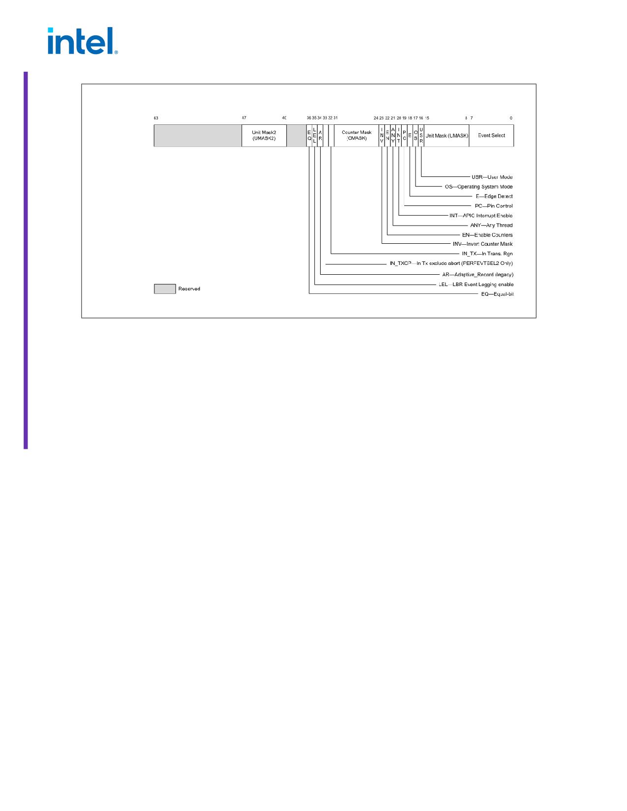
NEXT GENERATION PERFORMANCE MONITORING UNIT (PMU)
Figure 8-2. Layout of IA32_PERFEVTSELx Supporting Architectural Performance Monitoring Version 6
8.5.3
Equal Flag
Architectural performance monitoring version 6 introduces a new Equal (EQ) flag in the IA32_PERFEVTSELx MSRs.
It is supported if enumerated by CPUID.(EAX=23H, ECX=0):EBX[bit 1].
• EQ flag (bit 36): When the EQ flag is set and the INV flag is clear, the comparison evaluates to true if the
selected performance monitoring event (the event) is equal to the specified Counter Mask value (CMask). When
the EQ flag is set and the INV flag is set, the comparison evaluates to true if the event is less than the CMask
value and the event is not zero. Note that if the CMask is zero, the EQ flag is ignored.
8.6
LBR ENHANCEMENTS
Next generation PMU introduces additional enhancements to Last Branch Records (LBRs) with details provided in
the sub-sections that follow.
8.6.1
LBR Event Logging
LBR Event Logging provides a means to log PMU event data in LBRs. This event data can be used to provide some
causality information for the Cycle Time metadata currently recorded in the LBRs' IA32_LBR_x_INFO.CYC_CNT
field (also known as Timed LBR).
When a programmable counter is enabled for a precise event and LBR is enabled, setting EN_LBR_LOG (bit 35) in
the associated IA32_PERFEVTSELx MSR enables occurrences of the chosen event to be additionally logged in a new
IA32_LBR_INFO.PMCx_CNT field. This two-bit field represents the number of occurrences of the event since retire-
ment of the operation that last recorded an LBR entry, saturating at a value of 3. For example, this field is called
PMC0_CNT at bits 33:32 of the IA32_LBR_x_INFO MSR for programmable counter 0. The same bits in the
IA32_LER_x_INFO MSRs continue to be reserved.
If the event chosen in the IA32_PERFEVTSELx is MSR not precise, no counts will be logged in LBRs. The events that
are precise on a given platform can be found in the online event list: https://perfmon-events.intel.com/.
When using LBR Event Logging, software should keep consistent CPL filtering settings between LBR and PerfMon.
Keeping the OS/USR bits in the IA32_LBR_CTL MSR and in the IA32_PERFEVTSELx MSR consistent ensures that
only events that occur in one or more chosen modes are logged. Similarly, software should keep
8-10
Document Number: 319433-050
NEXT GENERATION PERFORMANCE MONITORING UNIT (PMU)
FREEZE_LBRS_ON_PMI and FREEZE_PERFMON_ON_PMI in the IA32_DEBUGCTL MSR consistent. Other counter
filtering in the IA32_PERFEVTSELx MSRs (e.g., INV, CMASK, EDGE, and IN_TX) should be cleared; otherwise the
behavior and PMCx_CNT values are undefined.
Per-counter support for LBR Event Logging is indicated by the “Event Logging Supported” bitmap in
CPUID.(EAX=01CH, ECX=0).ECX[19:16].
8.7
AUTO COUNTER RELOAD
Auto Counter Reload (ACR) provides a means for software to specify that, for each supported counter, the hard-
ware should automatically reload the counter to a specified initial value upon overflow of chosen counters. This
mechanism enables software to sample based on the relative rate of two (or more) events, such that a sample (PMI
or PEBS) is taken only if the rate of one event exceeds some threshold relative to the rate of another event. Taking
a PMI or PEBS only when the relative rate of perfmon events crosses a threshold can have significantly less perfor-
mance overhead than other techniques (e.g., taking a PMI every 1000 instructions in order to check the number of
mispredicts since the last PMI).
8.7.1
Discovery and Interface
CPUID.(EAX=23H, ECX=2):EAX indicates which programmable counters [n:0] support ACR. If a programmable
counter (PMC_GPn) supports ACR, an associated IA32_PMC_GPn_CFG_B MSR and an IA32_PMC_GPn_CFG_C MSR
are supported. Similarly, CPUID.(EAX=23H, ECX=2):EBX indicates which fixed-function counters [m:0] support
ACR. If a fixed-function counter (PMC_FXm) supports ACR, an associated IA32_PMC_FXm_CFG_B MSR and an
IA32_PMC_FXm_CFG_C MSR are supported.
See Table 8-7 for details about the following MSRs: IA32_PMC_GPn_CFG_B, IA32_PMC_GPn_CFG_C,
IA32_PMC_FXm_CFG_B, and IA32_PMC_FXm_CFG_C.
8.7.2
Configuration and Behavior
For a given counter IA32_PMC_GPn_CTR, bit fields in the IA32_PMC_GPn_CFG_B MSR indicate which counter(s)
can cause a reload of that counter:
• If GP counter ‘n’ is configured to do a reload when GP counter ‘x’ overflows (IA32_PMC_GPn_CFG_B.PMC[x] =
1) and counter ‘x’ isn't configured to avoid being monitored by ACR (IA32_PMC_GPx-
_CFG_B.PREVENT_RELOAD = 0), then that GP counter ‘n’ will be written with its reload value (in IA32_PMC_G-
Pn_CFG_C[31:0]) when counter ‘x’ (IA32_PMC_GPx_CTR) overflows.
• If GP counter ‘n’ is configured to do a reload when fixed-function counter ‘x’ overflows
(IA32_PMC_GPn_CFG_B.FIXED_CTR[x] = 1) and counter ‘x’ isn't configured to avoid being monitored by ACR
(IA32_PMC_FXx_CFG_B.PREVENT_RELOAD = 0), then that GP counter ‘n’ will be written with its reload value
(in IA32_PMC_GPn_CFG_C[31:0]) when fixed counter ‘x’ (IA32_PMC_FXx_CTR) overflows.
• If IA32_PMC_GPn_CFG.PREVENT_RELOAD=1, do not allow any counters to reload based on the overflow of
IA32_PMC_GPn_CTR even if PMCn=1 set in any IA32_PMC_*_CFG_B MSRs.
ACR will not reload IA32_PMC_GPn_CTR if counters are frozen (IA32_PERF_GLOBAL_STATUS.COUNTERS_FROZEN
= 1) or if IA32_PMC_GPn_CTR has already overflowed (IA32_PERF_GLOBAL_STATUS.PMCn_OVF = 1). If a PMI or
PEBS is taken due to a counter overflow, the PMI ISR or PEBS record can record the unmodified counter value
before reloading the counter. In race conditions, where IA32_PMC_GPn_CTR overflows in the same cycle as a
counter configured to reload the IA32_PMC_GPn_CTR on overflow, IA32_PMC_GPn_CTR will not be reloaded, and
IA32_PERF_GLOBAL_STATUS.PMCn_OVF will be set.
For counters that reload themselves (i.e., IA32_PMC_GPn_CFG_B.PMCn = 1), the overflow bit
(IA32_PERF_GLOBAL_STATUS.PMCn_OVF) will never be set. Instead, upon overflow, the counter will be immedi-
ately reloaded; thus, it is never in an overflowed state. There is an exception associated with PEBS; see Section
8.7.2.2.
The behavior is similar for reloading of fixed-function counters. For IA32_PMC_FXm_CTR, the reload value is stored
in IA32_PMC_FXm_CFG_C[31:0], and which counters cause reload of IA32_PMC_FXm_CTR is configured in
Document Number: 319433-050
8-11
NEXT GENERATION PERFORMANCE MONITORING UNIT (PMU)
IA32_PMC_FXm_CFG_B. PREVENT_RELOAD checks are also applied similar to the IA32_PMC_GPn CTRs explained
above.
8.7.2.1
Reload Precision
ACR reload is not guaranteed to be precise; in some cases, a small number of events may be lost during the time
between counter overflow and counter reload. However, when the reload happens, hardware will reload all config-
ured counters simultaneously.
8.7.2.2
PEBS Interaction
If a counter is configured to reload other counters with ACR and to take PEBS on overflow, the counter reload
actions will be taken only after the PEBS record has been written. This ensures that any counter values captured in
the PEBS record reflect the value before the reload occurs. Because the reload actions are taken after the PEBS
records are written, reloaded counter value will not account for the events which occurred during the process of
writing the PEBS record.
For a counter configured to reload itself and to take PEBS on overflow, the overflow bit associated with the counter
(in IA32_PERF_GLOBAL_STATUS) will be set from the time the counter overflows to the time the PEBS record is
written. This is required to ensure the PEBS record is not lost due to a VM exit taken during record generation. Once
the record is written, the overflow bit will be cleared, and the counter reloaded.
8.7.2.3
Precise Distribution (PDIST) Interaction
Precise distribution of PEBS events (PDIR) is not supported when such a counter is reloaded by ACR. For details on
PDIST, see Chapter 20, “Performance Monitoring,” of the Intel® 64 and IA-32 Architectures Software Developer’s
Manual, Volume 3B.
8-12
Document Number: 319433-050