Intel 64 and IA-32 Architectures. Software Developer’s Manual (Collection, 2023) - page 6
ARCHITECTURE COMPATIBILITY
23.18.7.3 FPREM1 Instruction
The 32-bit x87 FPUs compute a partial remainder according to IEEE Standard 754. This instruction does not exist
on the 16-bit IA-32 math coprocessors. The availability of the FPREM1 instruction has is no impact on existing soft-
ware.
23.18.7.4 FPREM Instruction
On the 32-bit x87 FPUs, the condition code flags C0, C3, C1 in the status word correctly reflect the three low-order
bits of the quotient following execution of the FPREM instruction. On the 16-bit IA-32 math coprocessors, the
quotient bits are incorrect when performing a reduction of (64N + M) when (N ≥ 1) and M is 1 or 2. This difference
does not affect existing software; software that works around the bug should not be affected.
23.18.7.5 FUCOM, FUCOMP, and FUCOMPP Instructions
When executing the FUCOM, FUCOMP, and FUCOMPP instructions, the 32-bit x87 FPUs perform unordered compare
according to IEEE Standard 754. These instructions do not exist on the 16-bit IA-32 math coprocessors. The avail-
ability of these new instructions has no impact on existing software.
23.18.7.6 FPTAN Instruction
On the 32-bit x87 FPUs, the range of the operand for the FPTAN instruction is much less restricted (| ST(0) | < 263)
than on earlier math coprocessors. The instruction reduces the operand internally using an internal π/4 constant
that is more accurate. The range of the operand is restricted to (| ST(0) | < π/4) on the 16-bit IA-32 math copro-
cessors; the operand must be reduced to this range using FPREM. This change has no impact on existing software.
See also sections 8.3.8 and section 8.3.10 of the Intel® 64 and IA-32 Architectures Software Developer’s Manual,
Volume 1, for more information on the accuracy of the FPTAN instruction.
23.18.7.7 Stack Overflow
On the 32-bit x87 FPUs, if an FPU stack overflow occurs when the invalid-operation exception is masked, the FPU
returns the real, integer, or BCD-integer indefinite value to the destination operand, depending on the instruction
being executed. On the 16-bit IA-32 math coprocessors, the original operand remains unchanged following a stack
overflow, but it is loaded into register ST(1). This difference has no impact on existing software.
23.18.7.8 FSIN, FCOS, and FSINCOS Instructions
On the 32-bit x87 FPUs, these instructions perform three common trigonometric functions. These instructions do
not exist on the 16-bit IA-32 math coprocessors. The availability of these instructions has no impact on existing
software, but using them provides a performance upgrade. See also sections 8.3.8 and section 8.3.10 of the Intel®
64 and IA-32 Architectures Software Developer’s Manual, Volume 1, for more information on the accuracy of the
FSIN, FCOS, and FSINCOS instructions.
23.18.7.9 FPATAN Instruction
On the 32-bit x87 FPUs, the range of operands for the FPATAN instruction is unrestricted. On the 16-bit IA-32 math
coprocessors, the absolute value of the operand in register ST(0) must be smaller than the absolute value of the
operand in register ST(1). This difference has impact on existing software.
23.18.7.10 F2XM1 Instruction
The 32-bit x87 FPUs support a wider range of operands (-1 < ST (0) < + 1) for the F2XM1 instruction. The
supported operand range for the 16-bit IA-32 math coprocessors is (0 ≤ ST(0) ≤ 0.5). This difference has no impact
on existing software.
Vol. 3B
23-13
ARCHITECTURE COMPATIBILITY
23.18.7.11 FLD Instruction
On the 32-bit x87 FPUs, when using the FLD instruction to load an extended-real value, a denormal-operand excep-
tion is not generated because the instruction is not arithmetic. The 16-bit IA-32 math coprocessors do report a
denormal-operand exception in this situation. This difference does not affect existing software.
On the 32-bit x87 FPUs, loading a denormal value that is in single- or double-real format causes the value to be
converted to extended-real format. Loading a denormal value on the 16-bit IA-32 math coprocessors causes the
value to be converted to an unnormal. If the next instruction is FXTRACT or FXAM, the 32-bit x87 FPUs will give a
different result than the 16-bit IA-32 math coprocessors. This change was made for IEEE Standard 754 compati-
bility.
On the 32-bit x87 FPUs, loading an SNaN that is in single- or double-real format causes the FPU to generate an
invalid-operation exception. The 16-bit IA-32 math coprocessors do not raise an exception when loading a signaling
NaN. The invalid-operation exception handler for 16-bit math coprocessor software needs to be updated to handle
this condition when porting software to 32-bit FPUs. This change was made for IEEE Standard 754 compatibility.
23.18.7.12 FXTRACT Instruction
On the 32-bit x87 FPUs, if the operand is 0 for the FXTRACT instruction, the divide-by-zero exception is reported
and -∞ is delivered to register ST(1). If the operand is +∞, no exception is reported. If the operand is 0 on the 16-
bit IA-32 math coprocessors, 0 is delivered to register ST(1) and no exception is reported. If the operand is +∞, the
invalid-operation exception is reported. These differences have no impact on existing software. Software usually
bypasses 0 and ∞. This change is due to the IEEE Standard 754 recommendation to fully support the “logb” func-
tion.
23.18.7.13 Load Constant Instructions
On 32-bit x87 FPUs, rounding control is in effect for the load constant instructions. Rounding control is not in effect
for the 16-bit IA-32 math coprocessors. Results for the FLDPI, FLDLN2, FLDLG2, and FLDL2E instructions are the
same as for the 16-bit IA-32 math coprocessors when rounding control is set to round to nearest or round to +∞.
They are the same for the FLDL2T instruction when rounding control is set to round to nearest, round to -∞, or
round to zero. Results are different from the 16-bit IA-32 math coprocessors in the least significant bit of the
mantissa if rounding control is set to round to -∞ or round to 0 for the FLDPI, FLDLN2, FLDLG2, and FLDL2E instruc-
tions; they are different for the FLDL2T instruction if round to +∞ is specified. These changes were implemented for
compatibility with IEEE Standard 754 for Floating-Point Arithmetic recommendations.
23.18.7.14 FXAM Instruction
With the 32-bit x87 FPUs, if the FPU encounters an empty register when executing the FXAM instruction, it not
generate combinations of C0 through C3 equal to 1101 or 1111. The 16-bit IA-32 math coprocessors may generate
these combinations, among others. This difference has no impact on existing software; it provides a performance
upgrade to provide repeatable results.
23.18.7.15 FSAVE and FSTENV Instructions
With the 32-bit x87 FPUs, the address of a memory operand pointer stored by FSAVE or FSTENV is undefined if the
previous floating-point instruction did not refer to memory
23.18.8 Transcendental Instructions
The floating-point results of the P6 family and Pentium processors for transcendental instructions in the core range
may differ from the Intel486 processors by about 2 or 3 ulps (see “Transcendental Instruction Accuracy” in Chapter
8, “Programming with the x87 FPU,” of the Intel® 64 and IA-32 Architectures Software Developer’s Manual, Volume
1). Condition code flag C1 of the status word may differ as a result. The exact threshold for underflow and overflow
will vary by a few ulps. The P6 family and Pentium processors’ results will have a worst case error of less than 1 ulp
when rounding to the nearest-even and less than 1.5 ulps when rounding in other modes. The transcendental
23-14
Vol. 3B
ARCHITECTURE COMPATIBILITY
instructions are guaranteed to be monotonic, with respect to the input operands, throughout the domain supported
by the instruction.
Transcendental instructions may generate different results in the round-up flag (C1) on the 32-bit x87 FPUs. The
round-up flag is undefined for these instructions on the 16-bit IA-32 math coprocessors. This difference has no
impact on existing software.
23.18.9 Obsolete Instructions and Undefined Opcodes
The 8087 math coprocessor instructions FENI and FDISI, and the Intel 287 math coprocessor instruction FSETPM
are treated as integer NOP instructions in the 32-bit x87 FPUs. If these opcodes are detected in the instruction
stream, no specific operation is performed and no internal states are affected. FSETPM informed the Intel 287 math
coprocessor that the processor was in protected mode. The 32-bit x87 FPUs handle all addressing and exception-
pointer information, whether in protected mode or not.
For compatibility with prior generations there are a few reserved x87 opcodes which do not result in an invalid-
opcode (#UD) exception, but rather result in the same behavior as existing defined x87 instructions. In the interest
of standardization, it is recommended that the opcodes defined in the Intel® 64 and IA-32 Architectures Software
Developer’s Manual, Volumes 2A, 2B, 2C, & 2D, be used for these operations for standardization.
• DCD0H through DCD7H - Behaves the same as FCOM, D8D0H through D8D7H.
• DCD8H through DCDFH - Behaves the same as FCOMP, D8D8H through D8DFH.
• DDC8H through DDCFH - Behaves the same as FXCH, D9C8H through D9CFH.
• DED0H through DED7H - Behaves the same as FCOMP, D8D8H through D8DFH.
• DFD0H through DFD7H - Behaves the same as FSTP, DDD8H through DDDFH.
• DFC8H through DFCFH - Behaves the same as FXCH, D9C8H through D9CFH.
• DFD8H through DFDFH - Behaves the same as FSTP, DDD8H through DDDFH.
There are a few reserved x87 opcodes which provide unique behavior but do not provide capabilities which are not
already available in the main instructions defined in the Intel® 64 and IA-32 Architectures Software Developer’s
Manual, Volumes 2A, 2B, 2C, & 2D.
• D9D8H through D9DFH - Behaves the same as FSTP (DDD8H through DDDFH) but won't cause a stack
underflow exception.
• DFC0H through DFC7H - Behaves the same as FFREE (DDC0H through DDD7H) with the addition of an x87
stack POP.
23.18.10 WAIT/FWAIT Prefix Differences
On the Intel486 processor, when a WAIT/FWAIT instruction precedes a floating-point instruction (one which itself
automatically synchronizes with the previous floating-point instruction), the WAIT/FWAIT instruction is treated as
a no-op. Pending floating-point exceptions from a previous floating-point instruction are processed not on the
WAIT/FWAIT instruction but on the floating-point instruction following the WAIT/FWAIT instruction. In such a case,
the report of a floating-point exception may appear one instruction later on the Intel486 processor than on a P6
family or Pentium FPU, or on Intel 387 math coprocessor.
23.18.11 Operands Split Across Segments and/or Pages
On the P6 family, Pentium, and Intel486 processor FPUs, when the first half of an operand to be written is inside a
page or segment and the second half is outside, a memory fault can cause the first half to be stored but not the
second half. In this situation, the Intel 387 math coprocessor stores nothing.
23.18.12 FPU Instruction Synchronization
On the 32-bit x87 FPUs, all floating-point instructions are automatically synchronized; that is, the processor auto-
matically waits until the previous floating-point instruction has completed before completing the next floating-point
Vol. 3B
23-15
ARCHITECTURE COMPATIBILITY
instruction. No explicit WAIT/FWAIT instructions are required to assure this synchronization. For the 8087 math
coprocessors, explicit waits are required before each floating-point instruction to ensure synchronization. Although
8087 programs having explicit WAIT instructions execute perfectly on the 32-bit IA-32 processors without reas-
sembly, these WAIT instructions are unnecessary.
23.19 SERIALIZING INSTRUCTIONS
Certain instructions have been defined to serialize instruction execution to ensure that modifications to flags, regis-
ters, and memory are completed before the next instruction is executed (or in P6 family processor terminology
“committed to machine state”). Because the P6 family processors use branch-prediction and out-of-order execu-
tion techniques to improve performance, instruction execution is not generally serialized until the results of an
executed instruction are committed to machine state (see Chapter 2, “Intel® 64 and IA-32 Architectures,” in the
Intel® 64 and IA-32 Architectures Software Developer’s Manual, Volume 1).
As a result, at places in a program or task where it is critical to have execution completed for all previous instruc-
tions before executing the next instruction (for example, at a branch, at the end of a procedure, or in multipro-
cessor dependent code), it is useful to add a serializing instruction. See Section 9.3, “Serializing Instructions,” for
more information on serializing instructions.
23.20 FPU AND MATH COPROCESSOR INITIALIZATION
Table 10-1 shows the states of the FPUs in the P6 family, Pentium, Intel486 processors and of the Intel 387 math
coprocessor and Intel 287 coprocessor following a power-up, reset, or INIT, or following the execution of an
FINIT/FNINIT instruction. The following is some additional compatibility information concerning the initialization of
x87 FPUs and math coprocessors.
23.20.1 Intel® 387 and Intel® 287 Math Coprocessor Initialization
Following an Intel386 processor reset, the processor identifies its coprocessor type (Intel® 287 or Intel® 387 DX
math coprocessor) by sampling its ERROR# input some time after the falling edge of RESET# signal and before
execution of the first floating-point instruction. The Intel 287 coprocessor keeps its ERROR# output in inactive
state after hardware reset; the Intel 387 coprocessor keeps its ERROR# output in active state after hardware
reset.
Upon hardware reset or execution of the FINIT/FNINIT instruction, the Intel 387 math coprocessor signals an error
condition. The P6 family, Pentium, and Intel486 processors, like the Intel 287 coprocessor, do not.
23.20.2 Intel486 SX Processor and Intel 487 SX Math Coprocessor Initialization
When initializing an Intel486 SX processor and an Intel 487 SX math coprocessor, the initialization routine should
check the presence of the math coprocessor and should set the FPU related flags (EM, MP, and NE) in control
register CR0 accordingly (see Section 2.5, “Control Registers,” for a complete description of these flags). Table 23-2
gives the recommended settings for these flags when the math coprocessor is present. The FSTCW instruction will
give a value of FFFFH for the Intel486 SX microprocessor and 037FH for the Intel 487 SX math coprocessor.
23-16
Vol. 3B
ARCHITECTURE COMPATIBILITY
Table 23-2. Recommended Values of the EM, MP, and NE Flags for Intel486 SX Microprocessor/Intel 487 SX Math
Coprocessor System
CR0 Flags
Intel486 SX Processor Only
Intel 487 SX Math Coprocessor Present
EM
1
0
MP
0
1
NE
1
0, for MS-DOS* systems
1, for user-defined exception handler
The EM and MP flags in register CR0 are interpreted as shown in Table 23-3.
Table 23-3. EM and MP Flag Interpretation
EM
MP
Interpretation
0
0
Floating-point instructions are passed to FPU; WAIT/FWAIT and other waiting-type instructions
ignore TS.
0
1
Floating-point instructions are passed to FPU; WAIT/FWAIT and other waiting-type instructions
test TS.
1
0
Floating-point instructions trap to emulator; WAIT/FWAIT and other waiting-type instructions
ignore TS.
1
1
Floating-point instructions trap to emulator; WAIT/FWAIT and other waiting-type instructions
test TS.
Following is an example code sequence to initialize the system and check for the presence of Intel486 SX
processor/Intel 487 SX math coprocessor.
fninit
fstcw mem_loc
mov ax, mem_loc
cmp ax, 037fh
jz Intel487_SX_Math_CoProcessor_present
;ax=037fh
jmp Intel486_SX_microprocessor_present
;ax=ffffh
If the Intel 487 SX math coprocessor is not present, the following code can be run to set the CR0 register for the
Intel486 SX processor.
mov eax, cr0
and eax, fffffffdh ;make MP=0
or eax, 0024h
;make EM=1, NE=1
mov cr0, eax
This initialization will cause any floating-point instruction to generate a device not available exception (#NM), inter-
rupt 7. The software emulation will then take control to execute these instructions. This code is not required if an
Intel 487 SX math coprocessor is present in the system. In that case, the typical initialization routine for the
Intel486 SX microprocessor will be adequate.
Also, when designing an Intel486 SX processor based system with an Intel 487 SX math coprocessor, timing loops
should be independent of frequency and clocks per instruction. One way to attain this is to implement these loops
in hardware and not in software (for example, BIOS).
23.21 CONTROL REGISTERS
The following sections identify the new control registers and control register flags and fields that were introduced
to the 32-bit IA-32 in various processor families. See Figure 2-7 for the location of these flags and fields in the
control registers.
Vol. 3B
23-17
ARCHITECTURE COMPATIBILITY
The Pentium III processor introduced one new control flag in control register CR4:
• OSXMMEXCPT (bit 10) - The OS will set this bit if it supports unmasked SIMD floating-point exceptions.
The Pentium II processor introduced one new control flag in control register CR4:
• OSFXSR (bit 9) - The OS supports saving and restoring the Pentium III processor state during context
switches.
The Pentium Pro processor introduced three new control flags in control register CR4:
• PAE (bit 5) - Physical address extension. Enables paging mechanism to reference extended physical addresses
when set; restricts physical addresses to 32 bits when clear (see also: Section 23.22.1.1, “Physical Memory
Addressing Extension”).
• PGE (bit 7) - Page global enable. Inhibits flushing of frequently-used or shared pages on CR3 writes (see also:
Section 23.22.1.2, “Global Pages”).
• PCE (bit 8) - Performance-monitoring counter enable. Enables execution of the RDPMC instruction at any
protection level.
The content of CR4 is 0H following a hardware reset.
Control register CR4 was introduced in the Pentium processor. This register contains flags that enable certain new
extensions provided in the Pentium processor:
• VME - Virtual-8086 mode extensions. Enables support for a virtual interrupt flag in virtual-8086 mode (see
Section 21.3, “Interrupt and Exception Handling in Virtual-8086 Mode”).
• PVI - Protected-mode virtual interrupts. Enables support for a virtual interrupt flag in protected mode (see
Section 21.4, “Protected-Mode Virtual Interrupts”).
• TSD - Time-stamp disable. Restricts the execution of the RDTSC instruction to procedures running at
privileged level 0.
• DE - Debugging extensions. Causes an undefined opcode (#UD) exception to be generated when debug
registers DR4 and DR5 are references for improved performance (see Section 23.23.3, “Debug Registers DR4
and DR5”).
• PSE - Page size extensions. Enables 4-MByte pages with 32-bit paging when set (see Section 4.3, “32-Bit
Paging”).
• MCE - Machine-check enable. Enables the machine-check exception, allowing exception handling for certain
hardware error conditions (see Chapter 16, “Machine-Check Architecture”).
The Intel486 processor introduced five new flags in control register CR0:
• NE - Numeric error. Enables the normal mechanism for reporting floating-point numeric errors.
• WP - Write protect. Write-protects read-only pages against supervisor-mode accesses.
• AM - Alignment mask. Controls whether alignment checking is performed. Operates in conjunction with the AC
(Alignment Check) flag.
• NW - Not write-through. Enables write-throughs and cache invalidation cycles when clear and disables invali-
dation cycles and write-throughs that hit in the cache when set.
• CD - Cache disable. Enables the internal cache when clear and disables the cache when set.
The Intel486 processor introduced two new flags in control register CR3:
• PCD - Page-level cache disable. The state of this flag is driven on the PCD# pin during bus cycles that are not
paged, such as interrupt acknowledge cycles, when paging is enabled. The PCD# pin is used to control caching
in an external cache on a cycle-by-cycle basis.
• PWT - Page-level write-through. The state of this flag is driven on the PWT# pin during bus cycles that are not
paged, such as interrupt acknowledge cycles, when paging is enabled. The PWT# pin is used to control write
through in an external cache on a cycle-by-cycle basis.
23-18
Vol. 3B
ARCHITECTURE COMPATIBILITY
23.22 MEMORY MANAGEMENT FACILITIES
The following sections describe the new memory management facilities available in the various IA-32 processors
and some compatibility differences.
23.22.1 New Memory Management Control Flags
The Pentium Pro processor introduced three new memory management features: physical memory addressing
extension, the global bit in page-table entries, and general support for larger page sizes. These features are only
available when operating in protected mode.
23.22.1.1 Physical Memory Addressing Extension
The new PAE (physical address extension) flag in control register CR4, bit 5, may enable additional address lines
on the processor, allowing extended physical addresses. This option can only be used when paging is enabled,
using a new page-table mechanism provided to support the larger physical address range (see Section 4.1, “Paging
Modes and Control Bits”).
23.22.1.2 Global Pages
The new PGE (page global enable) flag in control register CR4, bit 7, provides a mechanism for preventing
frequently used pages from being flushed from the translation lookaside buffer (TLB). When this flag is set,
frequently used pages (such as pages containing kernel procedures or common data tables) can be marked global
by setting the global flag in a page-directory or page-table entry.
On a task switch or a write to control register CR3 (which normally causes the TLBs to be flushed), the entries in
the TLB marked global are not flushed. Marking pages global in this manner prevents unnecessary reloading of the
TLB due to TLB misses on frequently used pages. See Section 4.10, “Caching Translation Information,” for a
detailed description of this mechanism.
23.22.1.3 Larger Page Sizes
The P6 family processors support large page sizes. For 32-bit paging, this facility is enabled with the PSE (page size
extension) flag in control register CR4, bit 4. When this flag is set, the processor supports either 4-KByte or 4-
MByte page sizes. PAE paging and 4-level paging1 support 2-MByte pages regardless of the value of CR4.PSE (see
Section 4.4, “PAE Paging,” and Section 4.5, “4-Level Paging and 5-Level Paging”). See Chapter 4, “Paging,” for
more information about large page sizes.
23.22.2 CD and NW Cache Control Flags
The CD and NW flags in control register CR0 were introduced in the Intel486 processor. In the P6 family and
Pentium processors, these flags are used to implement a writeback strategy for the data cache; in the Intel486
processor, they implement a write-through strategy. See Table 12-5 for a comparison of these bits on the P6 family,
Pentium, and Intel486 processors. For complete information on caching, see Chapter 12, “Memory Cache Control.”
23.22.3 Descriptor Types and Contents
Operating-system code that manages space in descriptor tables often contains an invalid value in the access-rights
field of descriptor-table entries to identify unused entries. Access rights values of 80H and 00H remain invalid for
the P6 family, Pentium, Intel486, Intel386, and Intel 286 processors. Other values that were invalid on the Intel
286 processor may be valid on the 32-bit processors because uses for these bits have been defined.
1. Earlier versions of this manual used the term “IA-32e paging” to identify 4-level paging.
Vol. 3B
23-19
ARCHITECTURE COMPATIBILITY
23.22.4 Changes in Segment Descriptor Loads
On the Intel386 processor, loading a segment descriptor always causes a locked read and write to set the accessed
bit of the descriptor. On the P6 family, Pentium, and Intel486 processors, the locked read and write occur only if the
bit is not already set.
23.23 DEBUG FACILITIES
The P6 family and Pentium processors include extensions to the Intel486 processor debugging support for break-
points. To use the new breakpoint features, it is necessary to set the DE flag in control register CR4.
23.23.1 Differences in Debug Register DR6
It is not possible to write a 1 to reserved bit 12 in debug status register DR6 on the P6 family and Pentium proces-
sors; however, it is possible to write a 1 in this bit on the Intel486 processor. See Table 10-1 for the different setting
of this register following a power-up or hardware reset.
23.23.2 Differences in Debug Register DR7
The P6 family and Pentium processors determines the type of breakpoint access by the R/W0 through R/W3 fields
in debug control register DR7 as follows:
00
Break on instruction execution only.
01
Break on data writes only.
10
Undefined if the DE flag in control register CR4 is cleared; break on I/O reads or writes but not instruction
fetches if the DE flag in control register CR4 is set.
11
Break on data reads or writes but not instruction fetches.
On the P6 family and Pentium processors, reserved bits 11, 12, 14, and 15 are hard-wired to 0. On the Intel486
processor, however, bit 12 can be set. See Table 10-1 for the different settings of this register following a power-up
or hardware reset.
23.23.3 Debug Registers DR4 and DR5
Although the DR4 and DR5 registers are documented as reserved, previous generations of processors aliased refer-
ences to these registers to debug registers DR6 and DR7, respectively. When debug extensions are not enabled
(the DE flag in control register CR4 is cleared), the P6 family and Pentium processors remain compatible with
existing software by allowing these aliased references. When debug extensions are enabled (the DE flag is set),
attempts to reference registers DR4 or DR5 will result in an invalid-opcode exception (#UD).
23.24 RECOGNITION OF BREAKPOINTS
For the Pentium processor, it is recommended that debuggers execute the LGDT instruction before returning to the
program being debugged to ensure that breakpoints are detected. This operation does not need to be performed
on the P6 family, Intel486, or Intel386 processors.
The implementation of test registers on the Intel486 processor used for testing the cache and TLB has been rede-
signed using MSRs on the P6 family and Pentium processors. (Note that MSRs used for this function are different
on the P6 family and Pentium processors.) The MOV to and from test register instructions generate invalid-opcode
exceptions (#UD) on the P6 family processors.
23-20
Vol. 3B
ARCHITECTURE COMPATIBILITY
23.25 EXCEPTIONS AND/OR EXCEPTION CONDITIONS
This section describes the new exceptions and exception conditions added to the 32-bit IA-32 processors and
implementation differences in existing exception handling. See Chapter 6, “Interrupt and Exception Handling,” for
a detailed description of the IA-32 exceptions.
The Pentium III processor introduced new state with the XMM registers. Computations involving data in these regis-
ters can produce exceptions. A new MXCSR control/status register is used to determine which exception or excep-
tions have occurred. When an exception associated with the XMM registers occurs, an interrupt is generated.
• SIMD floating-point exception (#XM, interrupt 19) - New exceptions associated with the SIMD floating-point
registers and resulting computations.
No new exceptions were added with the Pentium Pro and Pentium II processors. The set of available exceptions is
the same as for the Pentium processor. However, the following exception condition was added to the IA-32 with the
Pentium Pro processor:
• Machine-check exception (#MC, interrupt 18) - New exception conditions. Many exception conditions have
been added to the machine-check exception and a new architecture has been added for handling and reporting
on hardware errors. See Chapter 16, “Machine-Check Architecture,” for a detailed description of the new
conditions.
The following exceptions and/or exception conditions were added to the IA-32 with the Pentium processor:
• Machine-check exception (#MC, interrupt 18) - New exception. This exception reports parity and other
hardware errors. It is a model-specific exception and may not be implemented or implemented differently in
future processors. The MCE flag in control register CR4 enables the machine-check exception. When this bit is
clear (which it is at reset), the processor inhibits generation of the machine-check exception.
• General-protection exception (#GP, interrupt 13) - New exception condition added. An attempt to write a 1 to
a reserved bit position of a special register causes a general-protection exception to be generated.
• Page-fault exception (#PF, interrupt 14) - New exception condition added. When a 1 is detected in any of the
reserved bit positions of a page-table entry, page-directory entry, or page-directory pointer during address
translation, a page-fault exception is generated.
The following exception was added to the Intel486 processor:
• Alignment-check exception (#AC, interrupt 17) - New exception. Reports unaligned memory references when
alignment checking is being performed.
The following exceptions and/or exception conditions were added to the Intel386 processor:
• Divide-error exception (#DE, interrupt 0)
- Change in exception handling. Divide-error exceptions on the Intel386 processors always leave the saved
CS:IP value pointing to the instruction that failed. On the 8086 processor, the CS:IP value points to the next
instruction.
- Change in exception handling. The Intel386 processors can generate the largest negative number as a
quotient for the IDIV instruction (80H and 8000H). The 8086 processor generates a divide-error exception
instead.
• Invalid-opcode exception (#UD, interrupt 6) - New exception condition added. Improper use of the LOCK
instruction prefix can generate an invalid-opcode exception.
• Page-fault exception (#PF, interrupt 14) - New exception condition added. If paging is enabled in a 16-bit
program, a page-fault exception can be generated as follows. Paging can be used in a system with 16-bit tasks
if all tasks use the same page directory. Because there is no place in a 16-bit TSS to store the PDBR register,
switching to a 16-bit task does not change the value of the PDBR register. Tasks ported from the Intel 286
processor should be given 32-bit TSSs so they can make full use of paging.
• General-protection exception (#GP, interrupt 13) - New exception condition added. The Intel386 processor
sets a limit of 15 bytes on instruction length. The only way to violate this limit is by putting redundant prefixes
before an instruction. A general-protection exception is generated if the limit on instruction length is violated.
The 8086 processor has no instruction length limit.
Vol. 3B
23-21

ARCHITECTURE COMPATIBILITY
23.25.1 Machine-Check Architecture
The Pentium Pro processor introduced a new architecture to the IA-32 for handling and reporting on machine-check
exceptions. This machine-check architecture (described in detail in Chapter 16, “Machine-Check Architecture”)
greatly expands the ability of the processor to report on internal hardware errors.
23.25.2 Priority of Exceptions
The priority of exceptions are broken down into several major categories:
1. Traps on the previous instruction
2. External interrupts
3. Faults on fetching the next instruction
4. Faults in decoding the next instruction
5. Faults on executing an instruction
There are no changes in the priority of these major categories between the different processors, however, excep-
tions within these categories are implementation dependent and may change from processor to processor.
23.25.3 Exception Conditions of Legacy SIMD Instructions Operating on MMX Registers
MMX instructions and a subset of SSE, SSE2, SSSE3 instructions operate on MMX registers. The exception condi-
tions of these instructions are described in the following tables.
Table 23-4. Exception Conditions for Legacy SIMD/MMX Instructions with FP Exception and 16-Byte Alignment
Exception
Cause of Exception
X
X
X
X
If an unmasked SIMD floating-point exception and CR4.OSXMMEXCPT[bit 10] = 0.
If CR0.EM[bit 2] = 1.
Invalid Opcode,
X
X
X
X
If CR4.OSFXSR[bit 9] = 0.
#UD
X
X
X
X
If preceded by a LOCK prefix (F0H)
X
X
X
X
If any corresponding CPUID feature flag is ‘0’
#MF
X
X
X
X
If there is a pending X87 FPU exception
#NM
X
X
X
X
If CR0.TS[bit 3]=1
X
For an illegal address in the SS segment
Stack, SS(0)
X
If a memory address referencing the SS segment is in a non-canonical form
X
X
X
X
Legacy SSE: Memory operand is not 16-byte aligned
General Protec-
X
For an illegal memory operand effective address in the CS, DS, ES, FS or GS segments.
tion, #GP(0)
X
If the memory address is in a non-canonical form.
X
X
If any part of the operand lies outside the effective address space from 0 to FFFFH
#PF(fault-code)
X
X
X
For a page fault
#XM
X
X
X
X
If an unmasked SIMD floating-point exception and CR4.OSXMMEXCPT[bit 10] = 1
Applicable
CVTPD2PI, CVTTPD2PI
Instructions
23-22
Vol. 3B

ARCHITECTURE COMPATIBILITY
Table 23-5. Exception Conditions for Legacy SIMD/MMX Instructions with XMM and FP Exception
Exception
Cause of Exception
X
X
X
X
If an unmasked SIMD floating-point exception and CR4.OSXMMEXCPT[bit 10] = 0.
If CR0.EM[bit 2] = 1.
X
X
X
X
Invalid Opcode, #UD
If CR4.OSFXSR[bit 9] = 0.
X
X
X
X
If preceded by a LOCK prefix (F0H)
X
X
X
X
If any corresponding CPUID feature flag is ‘0’
#MF
X
X
X
X
If there is a pending X87 FPU exception
#NM
X
X
X
X
If CR0.TS[bit 3]=1
X
For an illegal address in the SS segment
Stack, SS(0)
X
If a memory address referencing the SS segment is in a non-canonical form
For an illegal memory operand effective address in the CS, DS, ES, FS or GS seg-
X
ments.
General Protection,
X
If the memory address is in a non-canonical form.
#GP(0)
If any part of the operand lies outside the effective address space from 0 to
X
X
FFFFH
#PF(fault-code)
X
X
X
For a page fault
Alignment Check
If alignment checking is enabled and an unaligned memory reference is made while
X
X
X
#AC(0)
the current privilege level is 3.
SIMD Floating-point
X
X
X
X
If an unmasked SIMD floating-point exception and CR4.OSXMMEXCPT[bit 10] = 1
Exception, #XM
Applicable Instruc-
CVTPI2PS, CVTPS2PI, CVTTPS2PI
tions
Vol. 3B
23-23

ARCHITECTURE COMPATIBILITY
Table 23-6. Exception Conditions for Legacy SIMD/MMX Instructions with XMM and without FP Exception
Exception
Cause of Exception
If CR0.EM[bit 2] = 1.
X
X
X
X
If CR4.OSFXSR[bit 9] = 0.
Invalid Opcode, #UD
X
X
X
X
If preceded by a LOCK prefix (F0H)
X
X
X
X
If any corresponding CPUID feature flag is ‘0’
#MF1
X
X
X
X
If there is a pending X87 FPU exception
#NM
X
X
X
X
If CR0.TS[bit 3]=1
X
For an illegal address in the SS segment
Stack, SS(0)
X
If a memory address referencing the SS segment is in a non-canonical form
For an illegal memory operand effective address in the CS, DS, ES, FS or GS seg-
X
ments.
General Protection,
X
If the memory address is in a non-canonical form.
#GP(0)
If any part of the operand lies outside the effective address space from 0 to
X
X
FFFFH
#PF(fault-code)
X
X
X
For a page fault
Alignment Check
If alignment checking is enabled and an unaligned memory reference is made
X
X
X
#AC(0)
while the current privilege level is 3.
Applicable Instruc-
CVTPI2PD
tions
NOTES:
1. Applies to “CVTPI2PD xmm, mm” but not “CVTPI2PD xmm, m64”.
23-24
Vol. 3B

ARCHITECTURE COMPATIBILITY
Table 23-7. Exception Conditions for SIMD/MMX Instructions with Memory Reference
Exception
Cause of Exception
X
X
X
X
If CR0.EM[bit 2] = 1.
Invalid Opcode, #UD
X
X
X
X
If preceded by a LOCK prefix (F0H)
X
X
X
X
If any corresponding CPUID feature flag is ‘0’
#MF
X
X
X
X
If there is a pending X87 FPU exception
#NM
X
X
X
X
If CR0.TS[bit 3]=1
X
For an illegal address in the SS segment
Stack, SS(0)
X
If a memory address referencing the SS segment is in a non-canonical form
For an illegal memory operand effective address in the CS, DS, ES, FS or GS seg-
X
ments.
General Protection,
#GP(0)
X
If the memory address is in a non-canonical form.
X
X
If any part of the operand lies outside the effective address space from 0 to FFFFH
#PF(fault-code)
X
X
X
For a page fault
Alignment Check
If alignment checking is enabled and an unaligned memory reference is made while
X
X
X
#AC(0)
the current privilege level is 3.
PABSB, PABSD, PABSW, PACKSSWB, PACKSSDW, PACKUSWB, PADDB, PADDD, PADDQ, PADDW, PADDSB,
PADDSW, PADDUSB, PADDUSW, PALIGNR, PAND, PANDN, PAVGB, PAVGW, PCMPEQB, PCMPEQD, PCMPEQW,
PCMPGTB, PCMPGTD, PCMPGTW, PHADDD, PHADDW, PHADDSW, PHSUBD, PHSUBW, PHSUBSW, PINSRW,
Applicable Instruc-
PMADDUBSW, PMADDWD, PMAXSW, PMAXUB, PMINSW, PMINUB, PMULHRSW, PMULHUW, PMULHW, PMULLW,
tions
PMULUDQ, PSADBW, PSHUFB, PSHUFW, PSIGNB PSIGND PSIGNW, PSLLW, PSLLD, PSLLQ, PSRAD, PSRAW,
PSRLW, PSRLD, PSRLQ, PSUBB, PSUBD, PSUBQ, PSUBW, PSUBSB, PSUBSW, PSUBUSB, PSUBUSW,
PUNPCKHBW, PUNPCKHWD, PUNPCKHDQ, PUNPCKLBW, PUNPCKLWD, PUNPCKLDQ, PXOR
Vol. 3B
23-25

ARCHITECTURE COMPATIBILITY
Table 23-8. Exception Conditions for Legacy SIMD/MMX Instructions without FP Exception
Exception
Cause of Exception
If CR0.EM[bit 2] = 1.
X
X
X
X
If ModR/M.mod ≠ 11b1
Invalid Opcode, #UD
X
X
X
X
If preceded by a LOCK prefix (F0H)
X
X
X
X
If any corresponding CPUID feature flag is ‘0’
#MF
X
X
X
X
If there is a pending X87 FPU exception
#NM
X
X
X
X
If CR0.TS[bit 3]=1
X
For an illegal address in the SS segment
Stack, SS(0)
X
If a memory address referencing the SS segment is in a non-canonical form
For an illegal memory operand effective address in the CS, DS, ES, FS or GS seg-
ments.
X
If the destination operand is in a non-writable segment.2
#GP(0)
If the DS, ES, FS, or GS register contains a NULL segment selector.3
X
If the memory address is in a non-canonical form.
X
X
If any part of the operand lies outside the effective address space from 0 to FFFFH
#PF(fault-code)
X
X
X
For a page fault
If alignment checking is enabled and an unaligned memory reference is made while
#AC(0)
X
X
X
the current privilege level is 3.
Applicable Instruc-
MASKMOVQ, MOVNTQ, “MOVQ (mmreg)”
tions
NOTES:
1. Applies to MASKMOVQ only.
2. Applies to MASKMOVQ and MOVQ (mmreg) only.
3. Applies to MASKMOVQ only.
23-26
Vol. 3B

ARCHITECTURE COMPATIBILITY
Table 23-9. Exception Conditions for Legacy SIMD/MMX Instructions without Memory Reference
Exception
Cause of Exception
X
X
X
X
If CR0.EM[bit 2] = 1.
Invalid Opcode, #UD
X
X
X
X
If preceded by a LOCK prefix (F0H)
X
X
X
X
If any corresponding CPUID feature flag is ‘0’
#MF
X
X
X
X
If there is a pending X87 FPU exception
#NM
X
X
If CR0.TS[bit 3]=1
Applicable Instruc-
PEXTRW, PMOVMSKB
tions
23.26 INTERRUPTS
The following differences in handling interrupts are found among the IA-32
processors.
23.26.1 Interrupt Propagation Delay
External hardware interrupts may be recognized on different instruction boundaries on the P6 family, Pentium,
Intel486, and Intel386 processors, due to the superscaler designs of the P6 family and Pentium processors. There-
fore, the EIP pushed onto the stack when servicing an interrupt may be different for the P6 family, Pentium,
Intel486, and Intel386 processors.
23.26.2 NMI Interrupts
After an NMI interrupt is recognized by the P6 family, Pentium, Intel486, Intel386, and Intel 286 processors, the
NMI interrupt is masked until the first IRET instruction is executed, unlike the 8086 processor.
23.26.3 IDT Limit
The LIDT instruction can be used to set a limit on the size of the IDT. A double-fault exception (#DF) is generated
if an interrupt or exception attempts to read a vector beyond the limit. Shutdown then occurs on the 32-bit IA-32
processors if the double-fault handler vector is beyond the limit. (The 8086 processor does not have a shutdown
mode nor a limit.)
23.27 ADVANCED PROGRAMMABLE INTERRUPT CONTROLLER (APIC)
The Advanced Programmable Interrupt Controller (APIC), referred to in this book as the local APIC, was intro-
duced into the IA-32 processors with the Pentium processor (beginning with the 735/90 and 815/100 models) and
is included in the Pentium 4, Intel Xeon, and P6 family processors. The features and functions of the local APIC are
derived from the Intel 82489DX external APIC, which was used with the Intel486 and early Pentium processors.
Additional refinements of the local APIC architecture were incorporated in the Pentium 4 and Intel Xeon processors.
Vol. 3B
23-27
ARCHITECTURE COMPATIBILITY
23.27.1 Software Visible Differences Between the Local APIC and the 82489DX
The following features in the local APIC features differ from those found in the 82489DX external APIC:
• When the local APIC is disabled by clearing the APIC software enable/disable flag in the spurious-interrupt
vector MSR, the state of its internal registers are unaffected, except that the mask bits in the LVT are all set to
block local interrupts to the processor. Also, the local APIC ceases accepting IPIs except for INIT, SMI, NMI, and
start-up IPIs. In the 82489DX, when the local unit is disabled, all the internal registers including the IRR, ISR,
and TMR are cleared and the mask bits in the LVT are set. In this state, the 82489DX local unit will accept only
the reset deassert message.
• In the local APIC, NMI and INIT (except for INIT deassert) are always treated as edge triggered interrupts, even
if programmed otherwise. In the 82489DX, these interrupts are always level triggered.
• In the local APIC, IPIs generated through the ICR are always treated as edge triggered (except INIT Deassert).
In the 82489DX, the ICR can be used to generate either edge or level triggered IPIs.
• In the local APIC, the logical destination register supports 8 bits; in the 82489DX, it supports 32 bits.
• In the local APIC, the APIC ID register is 4 bits wide; in the 82489DX, it is 8 bits wide.
• The remote read delivery mode provided in the 82489DX and local APIC for Pentium processors is not
supported in the local APIC in the Pentium 4, Intel Xeon, and P6 family processors.
• For the 82489DX, in the lowest priority delivery mode, all the target local APICs specified by the destination
field participate in the lowest priority arbitration. For the local APIC, only those local APICs which have free
interrupt slots will participate in the lowest priority arbitration.
23.27.2 New Features Incorporated in the Local APIC for the P6 Family and Pentium
Processors
The local APIC in the Pentium and P6 family processors have the following new features not found in the 82489DX
external APIC.
• Cluster addressing is supported in logical destination mode.
• Focus processor checking can be enabled/disabled.
• Interrupt input signal polarity can be programmed for the LINT0 and LINT1 pins.
• An SMI IPI is supported through the ICR and I/O redirection table.
• An error status register is incorporated into the LVT to log and report APIC errors.
In the P6 family processors, the local APIC incorporates an additional LVT register to handle performance moni-
toring counter interrupts.
23.27.3 New Features Incorporated in the Local APIC of the Pentium 4 and Intel Xeon
Processors
The local APIC in the Pentium 4 and Intel Xeon processors has the following new features not found in the P6 family
and Pentium processors and in the 82489DX.
• The local APIC ID is extended to 8 bits.
• An thermal sensor register is incorporated into the LVT to handle thermal sensor interrupts.
• The the ability to deliver lowest-priority interrupts to a focus processor is no longer supported.
• The flat cluster logical destination mode is not supported.
23.28 TASK SWITCHING AND TSS
This section identifies the implementation differences of task switching, additions to the TSS and the handling of
TSSs and TSS segment selectors.
23-28
Vol. 3B
ARCHITECTURE COMPATIBILITY
23.28.1 P6 Family and Pentium Processor TSS
When the virtual mode extensions are enabled (by setting the VME flag in control register CR4), the TSS in the P6
family and Pentium processors contain an interrupt redirection bit map, which is used in virtual-8086 mode to redi-
rect interrupts back to an 8086 program.
23.28.2 TSS Selector Writes
During task state saves, the Intel486 processor writes 2-byte segment selectors into a 32-bit TSS, leaving the
upper 16 bits undefined. For performance reasons, the P6 family and Pentium processors write 4-byte segment
selectors into the TSS, with the upper 2 bytes being 0. For compatibility reasons, code should not depend on the
value of the upper 16 bits of the selector in the TSS.
23.28.3 Order of Reads/Writes to the TSS
The order of reads and writes into the TSS is processor dependent. The P6 family and Pentium processors may
generate different page-fault addresses in control register CR2 in the same TSS area than the Intel486 and
Intel386 processors, if a TSS crosses a page boundary (which is not recommended).
23.28.4 Using A 16-Bit TSS with 32-Bit Constructs
Task switches using 16-bit TSSs should be used only for pure 16-bit code. Any new code written using 32-bit
constructs (operands, addressing, or the upper word of the EFLAGS register) should use only 32-bit TSSs. This is
due to the fact that the 32-bit processors do not save the upper 16 bits of EFLAGS to a 16-bit TSS. A task switch
back to a 16-bit task that was executing in virtual mode will never re-enable the virtual mode, as this flag was not
saved in the upper half of the EFLAGS value in the TSS. Therefore, it is strongly recommended that any code using
32-bit constructs use a 32-bit TSS to ensure correct behavior in a multitasking environment.
23.28.5 Differences in I/O Map Base Addresses
The Intel486 processor considers the TSS segment to be a 16-bit segment and wraps around the 64K boundary.
Any I/O accesses check for permission to access this I/O address at the I/O base address plus the I/O offset. If the
I/O map base address exceeds the specified limit of 0DFFFH, an I/O access will wrap around and obtain the permis-
sion for the I/O address at an incorrect location within the TSS. A TSS limit violation does not occur in this situation
on the Intel486 processor. However, the P6 family and Pentium processors consider the TSS to be a 32-bit segment
and a limit violation occurs when the I/O base address plus the I/O offset is greater than the TSS limit. By following
the recommended specification for the I/O base address to be less than 0DFFFH, the Intel486 processor will not
wrap around and access incorrect locations within the TSS for I/O port validation and the P6 family and Pentium
processors will not experience general-protection exceptions (#GP). Figure 23-1 demonstrates the different areas
accessed by the Intel486 and the P6 family and Pentium processors.
Vol. 3B
23-29
ARCHITECTURE COMPATIBILITY
Intel486 Processor
P6 family and Pentium Processors
FFFFH + 10H = Outside Segment
for I/O Validation
FFFFH
FFFFH
I/O Map
I/O Map
FFFFH
FFFFH
Base Addres
Base Addres
FFFFH + 10H = FH
for I/O Validation
0H
0H
I/O access at port 10H checks
I/O access at port 10H checks
bitmap at I/O map base address
bitmap at I/O address FFFFH + 10H,
FFFFH + 10H = offset 10H.
which exceeds segment limit.
Offset FH from beginning of
Wrap around does not occur,
TSS segment results because
general-protection exception (#GP)
wraparound occurs.
occurs.
Figure 23-1. I/O Map Base Address Differences
23.29 CACHE MANAGEMENT
The P6 family processors include two levels of internal caches: L1 (level 1) and L2 (level 2). The L1 cache is divided
into an instruction cache and a data cache; the L2 cache is a general-purpose cache. See Section 12.1, “Internal
Caches, TLBs, and Buffers,” for a description of these caches. (Note that although the Pentium II processor L2
cache is physically located on a separate chip in the cassette, it is considered an internal cache.)
The Pentium processor includes separate level 1 instruction and data caches. The data cache supports a writeback
(or alternatively write-through, on a line by line basis) policy for memory updates.
The Intel486 processor includes a single level 1 cache for both instructions and data.
The meaning of the CD and NW flags in control register CR0 have been redefined for the P6 family and Pentium
processors. For these processors, the recommended value (00B) enables writeback for the data cache of the
Pentium processor and for the L1 data cache and L2 cache of the P6 family processors. In the Intel486 processor,
setting these flags to (00B) enables write-through for the cache.
External system hardware can force the Pentium processor to disable caching or to use the write-through cache
policy should that be required. In the P6 family processors, the MTRRs can be used to override the CD and NW flags
(see Table 12-6).
The P6 family and Pentium processors support page-level cache management in the same manner as the Intel486
processor by using the PCD and PWT flags in control register CR3, the page-directory entries, and the page-table
entries. The Intel486 processor, however, is not affected by the state of the PWT flag since the internal cache of the
Intel486 processor is a write-through cache.
23.29.1 Self-Modifying Code with Cache Enabled
On the Intel486 processor, a write to an instruction in the cache will modify it in both the cache and memory. If the
instruction was prefetched before the write, however, the old version of the instruction could be the one executed.
To prevent this problem, it is necessary to flush the instruction prefetch unit of the Intel486 processor by coding a
jump instruction immediately after any write that modifies an instruction. The P6 family and Pentium processors,
however, check whether a write may modify an instruction that has been prefetched for execution. This check is
based on the linear address of the instruction. If the linear address of an instruction is found to be present in the
23-30
Vol. 3B
ARCHITECTURE COMPATIBILITY
prefetch queue, the P6 family and Pentium processors flush the prefetch queue, eliminating the need to code a
jump instruction after any writes that modify an instruction.
Because the linear address of the write is checked against the linear address of the instructions that have been
prefetched, special care must be taken for self-modifying code to work correctly when the physical addresses of the
instruction and the written data are the same, but the linear addresses differ. In such cases, it is necessary to
execute a serializing operation to flush the prefetch queue after the write and before executing the modified
instruction. See Section 9.3, “Serializing Instructions,” for more information on serializing instructions.
NOTE
The check on linear addresses described above is not in practice a concern for compatibility. Appli-
cations that include self-modifying code use the same linear address for modifying and fetching the
instruction. System software, such as a debugger, that might possibly modify an instruction using
a different linear address than that used to fetch the instruction must execute a serializing
operation, such as IRET, before the modified instruction is executed.
23.29.2 Disabling the L3 Cache
A unified third-level (L3) cache in processors based on Intel NetBurst microarchitecture (see Section 12.1,
“Internal Caches, TLBs, and Buffers”) provides the third-level cache disable flag, bit 6 of the IA32_MISC_ENABLE
MSR. The third-level cache disable flag allows the L3 cache to be disabled and enabled, independently of the L1 and
L2 caches (see Section 12.5.4, “Disabling and Enabling the L3 Cache”). The third-level cache disable flag applies
only to processors based on Intel NetBurst microarchitecture. Processors with L3 and based on other microarchi-
tectures do not support the third-level cache disable flag.
23.30 PAGING
This section identifies enhancements made to the paging mechanism and implementation differences in the paging
mechanism for various IA-32 processors.
23.30.1 Large Pages
The Pentium processor extended the memory management/paging facilities of the IA-32 to allow large (4 MBytes)
pages sizes (see Section 4.3, “32-Bit Paging”). The first P6 family processor (the Pentium Pro processor) added a
2 MByte page size to the IA-32 in conjunction with the physical address extension (PAE) feature (see Section 4.4,
“PAE Paging”).
The availability of large pages with 32-bit paging on any IA-32 processor can be determined via feature bit 3 (PSE)
of register EDX after the CPUID instruction has been execution with an argument of 1. (Large pages are always
available with PAE paging and 4-level paging.) Intel processors that do not support the CPUID instruction support
only 32-bit paging and do not support page size enhancements. (See “CPUID-CPU Identification” in Chapter 3,
“Instruction Set Reference, A-L,” in the Intel® 64 and IA-32 Architectures Software Developer’s Manual, Volume
2A, for more information on the CPUID instruction.)
23.30.2 PCD and PWT Flags
The PCD and PWT flags were introduced to the IA-32 in the Intel486 processor to control the caching of pages:
• PCD (page-level cache disable) flag-Controls caching on a page-by-page basis.
• PWT (page-level write-through) flag-Controls the write-through/writeback caching policy on a page-by-page
basis. Since the internal cache of the Intel486 processor is a write-through cache, it is not affected by the state
of the PWT flag.
Vol. 3B
23-31
ARCHITECTURE COMPATIBILITY
23.30.3 Enabling and Disabling Paging
Paging is enabled and disabled by loading a value into control register CR0 that modifies the PG flag. For backward
and forward compatibility with all IA-32 processors, Intel recommends that the following operations be performed
when enabling or disabling paging:
1. Execute a MOV CR0, REG instruction to either set (enable paging) or clear (disable paging) the PG flag.
2. Execute a near JMP instruction.
The sequence bounded by the MOV and JMP instructions should be identity mapped (that is, the instructions should
reside on a page whose linear and physical addresses are identical).
For the P6 family processors, the MOV CR0, REG instruction is serializing, so the jump operation is not required.
However, for backwards compatibility, the JMP instruction should still be included.
23.31 STACK OPERATIONS AND SUPERVISOR SOFTWARE
This section identifies the differences in the stack mechanism for the various IA-32 processors.
23.31.1 Selector Pushes and Pops
When pushing a segment selector onto the stack, the Pentium 4, Intel Xeon, P6 family, and Intel486 processors
decrement the ESP register by the operand size and then write 2 bytes. If the operand size is 32-bits, the upper two
bytes of the write are not modified. The Pentium processor decrements the ESP register by the operand size and
determines the size of the write by the operand size. If the operand size is 32-bits, the upper two bytes are written
as 0s.
When popping a segment selector from the stack, the Pentium 4, Intel Xeon, P6 family, and Intel486 processors
read 2 bytes and increment the ESP register by the operand size of the instruction. The Pentium processor deter-
mines the size of the read from the operand size and increments the ESP register by the operand size.
It is possible to align a 32-bit selector push or pop such that the operation generates an exception on a Pentium
processor and not on an Pentium 4, Intel Xeon, P6 family, or Intel486 processor. This could occur if the third and/or
fourth byte of the operation lies beyond the limit of the segment or if the third and/or fourth byte of the operation
is locate on a non-present or inaccessible page.
For a POP-to-memory instruction that meets the following conditions:
• The stack segment size is 16-bit.
• Any 32-bit addressing form with the SIB byte specifying ESP as the base register.
• The initial stack pointer is FFFCH (32-bit operand) or FFFEH (16-bit operand) and will wrap around to 0H as a
result of the POP operation.
The result of the memory write is implementation-specific. For example, in P6 family processors, the result of the
memory write is SS:0H plus any scaled index and displacement. In Pentium processors, the result of the memory
write may be either a stack fault (real mode or protected mode with stack segment size of 64 KByte), or write to
SS:10000H plus any scaled index and displacement (protected mode and stack segment size exceeds 64 KByte).
23.31.2 Error Code Pushes
The Intel486 processor implements the error code pushed on the stack as a 16-bit value. When pushed onto a 32-
bit stack, the Intel486 processor only pushes 2 bytes and updates ESP by 4. The P6 family and Pentium processors’
error code is a full 32 bits with the upper 16 bits set to zero. The P6 family and Pentium processors, therefore, push
4 bytes and update ESP by 4. Any code that relies on the state of the upper 16 bits may produce inconsistent
results.
23-32
Vol. 3B
ARCHITECTURE COMPATIBILITY
23.31.3 Fault Handling Effects on the Stack
During the handling of certain instructions, such as CALL and PUSHA, faults may occur in different sequences for
the different processors. For example, during far calls, the Intel486 processor pushes the old CS and EIP before a
possible branch fault is resolved. A branch fault is a fault from a branch instruction occurring from a segment limit
or access rights violation. If a branch fault is taken, the Intel486 and P6 family processors will have corrupted
memory below the stack pointer. However, the ESP register is backed up to make the instruction restartable. The
P6 family processors issue the branch before the pushes. Therefore, if a branch fault does occur, these processors
do not corrupt memory below the stack pointer. This implementation difference, however, does not constitute a
compatibility problem, as only values at or above the stack pointer are considered to be valid. Other operations
that encounter faults may also corrupt memory below the stack pointer and this behavior may vary on different
implementations.
23.31.4 Interlevel RET/IRET From a 16-Bit Interrupt or Call Gate
If a call or interrupt is made from a 32-bit stack environment through a 16-bit gate, only 16 bits of the old ESP can
be pushed onto the stack. On the subsequent RET/IRET, the 16-bit ESP is popped but the full 32-bit ESP is updated
since control is being resumed in a 32-bit stack environment. The Intel486 processor writes the SS selector into the
upper 16 bits of ESP. The P6 family and Pentium processors write zeros into the upper 16 bits.
23.32 MIXING 16- AND 32-BIT SEGMENTS
The features of the 16-bit Intel 286 processor are an object-code compatible subset of those of the 32-bit IA-32
processors. The D (default operation size) flag in segment descriptors indicates whether the processor treats a
code or data segment as a 16-bit or 32-bit segment; the B (default stack size) flag in segment descriptors indicates
whether the processor treats a stack segment as a 16-bit or 32-bit segment.
The segment descriptors used by the Intel 286 processor are supported by the 32-bit IA-32 processors if the Intel-
reserved word (highest word) of the descriptor is clear. On the 32-bit IA-32 processors, this word includes the
upper bits of the base address and the segment limit.
The segment descriptors for data segments, code segments, local descriptor tables (there are no descriptors for
global descriptor tables), and task gates are the same for the 16- and 32-bit processors. Other 16-bit descriptors
(TSS segment, call gate, interrupt gate, and trap gate) are supported by the 32-bit processors.
The 32-bit processors also have descriptors for TSS segments, call gates, interrupt gates, and trap gates that
support the 32-bit architecture. Both kinds of descriptors can be used in the same system.
For those segment descriptors common to both 16- and 32-bit processors, clear bits in the reserved word cause the
32-bit processors to interpret these descriptors exactly as an Intel 286 processor does, that is:
• Base Address - The upper 8 bits of the 32-bit base address are clear, which limits base addresses to 24 bits.
• Limit - The upper 4 bits of the limit field are clear, restricting the value of the limit field to 64 KBytes.
• Granularity bit - The G (granularity) flag is clear, indicating the value of the 16-bit limit is interpreted in units
of 1 byte.
• Big bit - In a data-segment descriptor, the B flag is clear in the segment descriptor used by the 32-bit
processors, indicating the segment is no larger than 64 KBytes.
• Default bit - In a code-segment descriptor, the D flag is clear, indicating 16-bit addressing and operands are
the default. In a stack-segment descriptor, the D flag is clear, indicating use of the SP register (instead of the
ESP register) and a 64-KByte maximum segment limit.
For information on mixing 16- and 32-bit code in applications, see Chapter 22, “Mixing 16-Bit and 32-Bit Code.”
23.33 SEGMENT AND ADDRESS WRAPAROUND
This section discusses differences in segment and address wraparound between the P6 family, Pentium, Intel486,
Intel386, Intel 286, and 8086 processors.
Vol. 3B
23-33
ARCHITECTURE COMPATIBILITY
23.33.1 Segment Wraparound
On the 8086 processor, an attempt to access a memory operand that crosses offset 65,535 or 0FFFFH or offset 0
(for example, moving a word to offset 65,535 or pushing a word when the stack pointer is set to 1) causes the
offset to wrap around modulo 65,536 or 010000H. With the Intel 286 processor, any base and offset combination
that addresses beyond 16 MBytes wraps around to the 1 MByte of the address space. The P6 family, Pentium,
Intel486, and Intel386 processors in real-address mode generate an exception in these cases:
• A general-protection exception (#GP) if the segment is a data segment (that is, if the CS, DS, ES, FS, or GS
register is being used to address the segment).
• A stack-fault exception (#SS) if the segment is a stack segment (that is, if the SS register is being used).
An exception to this behavior occurs when a stack access is data aligned, and the stack pointer is pointing to the
last aligned piece of data that size at the top of the stack (ESP is FFFFFFFCH). When this data is popped, no
segment limit violation occurs and the stack pointer will wrap around to 0.
The address space of the P6 family, Pentium, and Intel486 processors may wraparound at 1 MByte in real-address
mode. An external A20M# pin forces wraparound if enabled. On Intel 8086 processors, it is possible to specify
addresses greater than 1 MByte. For example, with a selector value FFFFH and an offset of FFFFH, the effective
address would be 10FFEFH (1 MByte plus 65519 bytes). The 8086 processor, which can form addresses up to 20
bits long, truncates the uppermost bit, which “wraps” this address to FFEFH. However, the P6 family, Pentium, and
Intel486 processors do not truncate this bit if A20M# is not enabled.
If a stack operation wraps around the address limit, shutdown occurs. (The 8086 processor does not have a shut-
down mode or a limit.)
The behavior when executing near the limit of a 4-GByte selector (limit = FFFFFFFFH) is different between the
Pentium Pro and the Pentium 4 family of processors. On the Pentium Pro, instructions which cross the limit -- for
example, a two byte instruction such as INC EAX that is encoded as FFH C0H starting exactly at the limit faults for
a segment violation (a one byte instruction at FFFFFFFFH does not cause an exception). Using the Pentium 4 micro-
processor family, neither of these situations causes a fault.
Segment wraparound and the functionality of A20M# is used primarily by older operating systems and not used by
modern operating systems. On newer Intel 64 processors, A20M# may be absent.
23.34 STORE BUFFERS AND MEMORY ORDERING
The Pentium 4, Intel Xeon, and P6 family processors provide a store buffer for temporary storage of writes (stores)
to memory (see Section 12.10, “Store Buffer”). Writes stored in the store buffer(s) are always written to memory
in program order, with the exception of “fast string” store operations (see Section 9.2.4, “Fast-String Operation and
Out-of-Order Stores”).
The Pentium processor has two store buffers, one corresponding to each of the pipelines. Writes in these buffers
are always written to memory in the order they were generated by the processor core.
It should be noted that only memory writes are buffered and I/O writes are not. The Pentium 4, Intel Xeon, P6
family, Pentium, and Intel486 processors do not synchronize the completion of memory writes on the bus and
instruction execution after a write. An I/O, locked, or serializing instruction needs to be executed to synchronize
writes with the next instruction (see Section 9.3, “Serializing Instructions”).
The Pentium 4, Intel Xeon, and P6 family processors use processor ordering to maintain consistency in the order
that data is read (loaded) and written (stored) in a program and the order the processor actually carries out the
reads and writes. With this type of ordering, reads can be carried out speculatively and in any order, reads can pass
buffered writes, and writes to memory are always carried out in program order. (See Section 9.2, “Memory
Ordering,” for more information about processor ordering.) The Pentium III processor introduced a new instruction
to serialize writes and make them globally visible. Memory ordering issues can arise between a producer and a
consumer of data. The SFENCE instruction provides a performance-efficient way of ensuring ordering between
routines that produce weakly-ordered results and routines that consume this data.
No re-ordering of reads occurs on the Pentium processor, except under the condition noted in Section 9.2.1,
“Memory Ordering in the Intel® Pentium® and Intel486™ Processors,” and in the following paragraph describing
the Intel486 processor.
23-34
Vol. 3B
ARCHITECTURE COMPATIBILITY
Specifically, the store buffers are flushed before the IN instruction is executed. No reads (as a result of cache miss)
are reordered around previously generated writes sitting in the store buffers. The implication of this is that the
store buffers will be flushed or emptied before a subsequent bus cycle is run on the external bus.
On both the Intel486 and Pentium processors, under certain conditions, a memory read will go onto the external
bus before the pending memory writes in the buffer even though the writes occurred earlier in the program execu-
tion. A memory read will only be reordered in front of all writes pending in the buffers if all writes pending in the
buffers are cache hits and the read is a cache miss. Under these conditions, the Intel486 and Pentium processors
will not read from an external memory location that needs to be updated by one of the pending writes.
During a locked bus cycle, the Intel486 processor will always access external memory, it will never look for the
location in the on-chip cache. All data pending in the Intel486 processor's store buffers will be written to memory
before a locked cycle is allowed to proceed to the external bus. Thus, the locked bus cycle can be used for elimi-
nating the possibility of reordering read cycles on the Intel486 processor. The Pentium processor does check its
cache on a read-modify-write access and, if the cache line has been modified, writes the contents back to memory
before locking the bus. The P6 family processors write to their cache on a read-modify-write operation (if the
access does not split across a cache line) and does not write back to system memory. If the access does split across
a cache line, it locks the bus and accesses system memory.
I/O reads are never reordered in front of buffered memory writes on an IA-32 processor. This ensures an update of
all memory locations before reading the status from an I/O device.
23.35 BUS LOCKING
The Intel 286 processor performs the bus locking differently than the Intel P6 family, Pentium, Intel486, and
Intel386 processors. Programs that use forms of memory locking specific to the Intel 286 processor may not run
properly when run on later processors.
A locked instruction is guaranteed to lock only the area of memory defined by the destination operand, but may
lock a larger memory area. For example, typical 8086 and Intel 286 configurations lock the entire physical memory
space. Programmers should not depend on this.
On the Intel 286 processor, the LOCK prefix is sensitive to IOPL. If the CPL is greater than the IOPL, a general-
protection exception (#GP) is generated. On the Intel386 DX, Intel486, and Pentium, and P6 family processors, no
check against IOPL is performed.
The Pentium processor automatically asserts the LOCK# signal when acknowledging external interrupts. After
signaling an interrupt request, an external interrupt controller may use the data bus to send the interrupt vector to
the processor. After receiving the interrupt request signal, the processor asserts LOCK# to ensure that no other
data appears on the data bus until the interrupt vector is received. This bus locking does not occur on the P6 family
processors.
23.36 BUS HOLD
Unlike the 8086 and Intel 286 processors, but like the Intel386 and Intel486 processors, the P6 family and Pentium
processors respond to requests for control of the bus from other potential bus masters, such as DMA controllers,
between transfers of parts of an unaligned operand, such as two words which form a doubleword. Unlike the
Intel386 processor, the P6 family, Pentium, and Intel486 processors respond to bus hold during reset initialization.
23.37 MODEL-SPECIFIC EXTENSIONS TO THE IA-32
Certain extensions to the IA-32 are specific to a processor or family of IA-32 processors and may not be imple-
mented or implemented in the same way in future processors. The following sections describe these model-specific
extensions. The CPUID instruction indicates the availability of some of the model-specific features.
Vol. 3B
23-35
ARCHITECTURE COMPATIBILITY
23.37.1 Model-Specific Registers
The Pentium processor introduced a set of model-specific registers (MSRs) for use in controlling hardware functions
and performance monitoring. To access these MSRs, two new instructions were added to the IA-32 architecture:
read MSR (RDMSR) and write MSR (WRMSR). The MSRs in the Pentium processor are not guaranteed to be dupli-
cated or provided in the next generation IA-32 processors.
The P6 family processors greatly increased the number of MSRs available to software. See Chapter 2, “Model-
Specific Registers (MSRs)‚” in the Intel® 64 and IA-32 Architectures Software Developer’s Manual, Volume 4, for a
complete list of the available MSRs. The new registers control the debug extensions, the performance counters, the
machine-check exception capability, the machine-check architecture, and the MTRRs. These registers are acces-
sible using the RDMSR and WRMSR instructions. Specific information on some of these new MSRs is provided in the
following sections. As with the Pentium processor MSR, the P6 family processor MSRs are not guaranteed to be
duplicated or provided in the next generation IA-32 processors.
23.37.2 RDMSR and WRMSR Instructions
The RDMSR (read model-specific register) and WRMSR (write model-specific register) instructions recognize a
much larger number of model-specific registers in the P6 family processors. (See “RDMSR-Read from Model
Specific Register” and “WRMSR-Write to Model Specific Register” in the Intel® 64 and IA-32 Architectures Soft-
ware Developer’s Manual, Volumes 2A, 2B, 2C, & 2D, for more information.)
23.37.3 Memory Type Range Registers
Memory type range registers (MTRRs) are a new feature introduced into the IA-32 in the Pentium Pro processor.
MTRRs allow the processor to optimize memory operations for different types of memory, such as RAM, ROM, frame
buffer memory, and memory-mapped I/O.
MTRRs are MSRs that contain an internal map of how physical address ranges are mapped to various types of
memory. The processor uses this internal memory map to determine the cacheability of various physical memory
locations and the optimal method of accessing memory locations. For example, if a memory location is specified in
an MTRR as write-through memory, the processor handles accesses to this location as follows. It reads data from
that location in lines and caches the read data or maps all writes to that location to the bus and updates the cache
to maintain cache coherency. In mapping the physical address space with MTRRs, the processor recognizes five
types of memory: uncacheable (UC), uncacheable, speculatable, write-combining (WC), write-through (WT),
write-protected (WP), and writeback (WB).
Earlier IA-32 processors (such as the Intel486 and Pentium processors) used the KEN# (cache enable) pin and
external logic to maintain an external memory map and signal cacheable accesses to the processor. The MTRR
mechanism simplifies hardware designs by eliminating the KEN# pin and the external logic required to drive it.
See Chapter 10, “Processor Management and Initialization,” and Chapter 2, “Model-Specific Registers (MSRs)‚” in
the Intel® 64 and IA-32 Architectures Software Developer’s Manual, Volume 4, for more information on the MTRRs.
23.37.4 Machine-Check Exception and Architecture
The Pentium processor introduced a new exception called the machine-check exception (#MC, interrupt 18). This
exception is used to detect hardware-related errors, such as a parity error on a read cycle.
The P6 family processors extend the types of errors that can be detected and that generate a machine-check
exception. It also provides a new machine-check architecture for recording information about a machine-check
error and provides extended recovery capability.
The machine-check architecture provides several banks of reporting registers for recording machine-check errors.
Each bank of registers is associated with a specific hardware unit in the processor. The primary focus of the
machine checks is on bus and interconnect operations; however, checks are also made of translation lookaside
buffer (TLB) and cache operations.
23-36
Vol. 3B
ARCHITECTURE COMPATIBILITY
The machine-check architecture can correct some errors automatically and allow for reliable restart of instruction
execution. It also collects sufficient information for software to use in correcting other machine errors not corrected
by hardware.
See Chapter 16, “Machine-Check Architecture,” for more information on the machine-check exception and the
machine-check architecture.
23.37.5 Performance-Monitoring Counters
The P6 family and Pentium processors provide two performance-monitoring counters for use in monitoring internal
hardware operations. The number of performance monitoring counters and associated programming interfaces
may be implementation specific for Pentium 4 processors, Pentium M processors. Later processors may have
implemented these as part of an architectural performance monitoring feature. The architectural and non-architec-
tural performance monitoring interfaces for different processor families are described in Chapter 20, “Performance
Monitoring.” https://perfmon-events.intel.com/ lists all the events that can be counted for architectural perfor-
mance monitoring events and non-architectural events. The counters are set up, started, and stopped using two
MSRs and the RDMSR and WRMSR instructions. For the P6 family processors, the current count for a particular
counter can be read using the new RDPMC instruction.
The performance-monitoring counters are useful for debugging programs, optimizing code, diagnosing system fail-
ures, or refining hardware designs. See Chapter 20, “Performance Monitoring,” for more information on these
counters.
23.38 TWO WAYS TO RUN INTEL 286 PROCESSOR TASKS
When porting 16-bit programs to run on 32-bit IA-32 processors, there are two approaches to consider:
• Porting an entire 16-bit software system to a 32-bit processor, complete with the old operating system, loader,
and system builder. Here, all tasks will have 16-bit TSSs. The 32-bit processor is being used as if it were a faster
version of the 16-bit processor.
• Porting selected 16-bit applications to run in a 32-bit processor environment with a 32-bit operating system,
loader, and system builder. Here, the TSSs used to represent 286 tasks should be changed to 32-bit TSSs. It is
possible to mix 16 and 32-bit TSSs, but the benefits are small and the problems are great. All tasks in a 32-bit
software system should have 32-bit TSSs. It is not necessary to change the 16-bit object modules themselves;
TSSs are usually constructed by the operating system, by the loader, or by the system builder. See Chapter 22,
“Mixing 16-Bit and 32-Bit Code,” for more detailed information about mixing 16-bit and 32-bit code.
Because the 32-bit processors use the contents of the reserved word of 16-bit segment descriptors, 16-bit
programs that place values in this word may not run correctly on the 32-bit processors.
23.39 INITIAL STATE OF PENTIUM, PENTIUM PRO AND PENTIUM 4 PROCESSORS
Table 23-10 shows the state of the flags and other registers following power-up for the Pentium, Pentium Pro and
Pentium 4 processors. The state of control register CR0 is 60000010H (see Figure 10-1 “Contents of CR0 Register
after Reset” in the Intel® 64 and IA-32 Architectures Software Developer’s Manual, Volume 3A). This places the
processor in real-address mode with paging disabled.
Table 23-10. Processor State Following Power-up/Reset/INIT for Pentium, Pentium Pro and Pentium 4 Processors
Register
Pentium 4 Processor
Pentium Pro Processor
Pentium Processor
EFLAGS1
00000002H
00000002H
00000002H
EIP
0000FFF0H
0000FFF0H
0000FFF0H
CR0
60000010H2
60000010H2
60000010H2
CR2, CR3, CR4
00000000H
00000000H
00000000H
Vol. 3B
23-37

ARCHITECTURE COMPATIBILITY
Table 23-10. Processor State Following Power-up/Reset/INIT for Pentium, Pentium Pro and Pentium 4 Processors
Register
Pentium 4 Processor
Pentium Pro Processor
Pentium Processor
CS
Selector = F000H
Selector = F000H
Selector = F000H
Base = FFFF0000H
Base = FFFF0000H
Base = FFFF0000H
Limit = FFFFH
Limit = FFFFH
Limit = FFFFH
AR = Present, R/W, Accessed
AR = Present, R/W, Accessed
AR = Present, R/W, Accessed
SS, DS, ES, FS, GS
Selector = 0000H
Selector = 0000H
Selector = 0000H
Base = 00000000H
Base = 00000000H
Base = 00000000H
Limit = FFFFH
Limit = FFFFH
Limit = FFFFH
AR = Present, R/W, Accessed
AR = Present, R/W, Accessed
AR = Present, R/W, Accessed
EDX
00000FxxH
000n06xxH3
000005xxH
EAX
04
04
04
EBX, ECX, ESI, EDI, EBP,
00000000H
00000000H
00000000H
ESP
ST0 through ST75
Pwr up or Reset: +0.0
Pwr up or Reset: +0.0
Pwr up or Reset: +0.0
FINIT/FNINIT: Unchanged
FINIT/FNINIT: Unchanged
FINIT/FNINIT: Unchanged
x87 FPU Control
Pwr up or Reset: 0040H
Pwr up or Reset: 0040H
Pwr up or Reset: 0040H
Word5
FINIT/FNINIT: 037FH
FINIT/FNINIT: 037FH
FINIT/FNINIT: 037FH
x87 FPU Status Word5
Pwr up or Reset: 0000H
Pwr up or Reset: 0000H
Pwr up or Reset: 0000H
FINIT/FNINIT: 0000H
FINIT/FNINIT: 0000H
FINIT/FNINIT: 0000H
x87 FPU Tag Word5
Pwr up or Reset: 5555H
Pwr up or Reset: 5555H
Pwr up or Reset: 5555H
FINIT/FNINIT: FFFFH
FINIT/FNINIT: FFFFH
FINIT/FNINIT: FFFFH
x87 FPU Data
Pwr up or Reset: 0000H
Pwr up or Reset: 0000H
Pwr up or Reset: 0000H
Operand and CS Seg.
FINIT/FNINIT: 0000H
FINIT/FNINIT: 0000H
FINIT/FNINIT: 0000H
Selectors5
x87 FPU Data
Pwr up or Reset:
Pwr up or Reset:
Pwr up or Reset:
Operand and Inst.
00000000H
00000000H
00000000H
Pointers5
FINIT/FNINIT: 00000000H
FINIT/FNINIT: 00000000H
FINIT/FNINIT: 00000000H
MM0 through MM75
Pwr up or Reset:
Pentium II and Pentium III
Pentium with MMX Technology
0000000000000000H
Processors Only-
Only-
INIT or FINIT/FNINIT:
Pwr up or Reset:
Pwr up or Reset:
Unchanged
0000000000000000H
0000000000000000H
INIT or FINIT/FNINIT:
INIT or FINIT/FNINIT:
Unchanged
Unchanged
XMM0 through XMM7
Pwr up or Reset: 0H
If CPUID.01H:SSE is 1 -
NA
INIT: Unchanged
Pwr up or Reset: 0H
INIT: Unchanged
MXCSR
Pwr up or Reset: 1F80H
Pentium III processor only-
NA
INIT: Unchanged
Pwr up or Reset: 1F80H
INIT: Unchanged
GDTR, IDTR
Base = 00000000H
Base = 00000000H
Base = 00000000H
Limit = FFFFH
Limit = FFFFH
Limit = FFFFH
AR = Present, R/W
AR = Present, R/W
AR = Present, R/W
LDTR, Task Register
Selector = 0000H
Selector = 0000H
Selector = 0000H
Base = 00000000H
Base = 00000000H
Base = 00000000H
Limit = FFFFH
Limit = FFFFH
Limit = FFFFH
AR = Present, R/W
AR = Present, R/W
AR = Present, R/W
DR0, DR1, DR2, DR3
00000000H
00000000H
00000000H
DR6
FFFF0FF0H
FFFF0FF0H
FFFF0FF0H
23-38
Vol. 3B

ARCHITECTURE COMPATIBILITY
Table 23-10. Processor State Following Power-up/Reset/INIT for Pentium, Pentium Pro and Pentium 4 Processors
Register
Pentium 4 Processor
Pentium Pro Processor
Pentium Processor
DR7
00000400H
00000400H
00000400H
Time-Stamp Counter
Power up or Reset: 0H
Power up or Reset: 0H
Power up or Reset: 0H
INIT: Unchanged
INIT: Unchanged
INIT: Unchanged
Perf. Counters and
Power up or Reset: 0H
Power up or Reset: 0H
Power up or Reset: 0H
Event Select
INIT: Unchanged
INIT: Unchanged
INIT: Unchanged
All Other MSRs
Pwr up or Reset:
Pwr up or Reset:
Pwr up or Reset:
Undefined
Undefined
Undefined
INIT: Unchanged
INIT: Unchanged
INIT: Unchanged
Data and Code Cache,
Invalid6
Invalid6
Invalid6
TLBs
Fixed MTRRs
Pwr up or Reset: Disabled
Pwr up or Reset: Disabled
Not Implemented
INIT: Unchanged
INIT: Unchanged
Variable MTRRs
Pwr up or Reset: Disabled
Pwr up or Reset: Disabled
Not Implemented
INIT: Unchanged
INIT: Unchanged
Machine-Check
Pwr up or Reset:
Pwr up or Reset:
Not Implemented
Architecture
Undefined
Undefined
INIT: Unchanged
INIT: Unchanged
APIC
Pwr up or Reset: Enabled
Pwr up or Reset: Enabled
Pwr up or Reset: Enabled
INIT: Unchanged
INIT: Unchanged
INIT: Unchanged
R8-R157
0000000000000000H
0000000000000000H
N.A.
XMM8-XMM157
Pwr up or Reset: 0H
Pwr up or Reset: 0H
N.A.
INIT: Unchanged
INIT: Unchanged
NOTES:
1. The 10 most-significant bits of the EFLAGS register are undefined following a reset. Software should not depend on the states of
any of these bits.
2. The CD and NW flags are unchanged, bit 4 is set to 1, all other bits are cleared.
3. Where “n” is the Extended Model Value for the respective processor.
4. If Built-In Self-Test (BIST) is invoked on power up or reset, EAX is 0 only if all tests passed. (BIST cannot be invoked during an INIT.)
5. The state of the x87 FPU and MMX registers is not changed by the execution of an INIT.
6. Internal caches are invalid after power-up and RESET, but left unchanged with an INIT.
7. If the processor supports IA-32e mode.
Vol. 3B
23-39
ARCHITECTURE COMPATIBILITY
23-40
Vol. 3B
15.Updates to Chapter 25, Volume 3C
Change bars and violet text show changes to Chapter 25 of the Intel® 64 and IA-32 Architectures Software
Developer’s Manual, Volume 3C: System Programming Guide, Part 3.
------------------------------------------------------------------------------------------
Changes to this chapter:
• Updated Section 25.9.1, “Basic VM-Exit Information,” to add bits 25 and 26 to the VMCS Exit Reason field.
Intel® 64 and IA-32 Architectures Software Developer’s Manual Documentation Changes
14
CHAPTER 25
VIRTUAL MACHINE CONTROL STRUCTURES
25.1
OVERVIEW
A logical processor uses virtual-machine control data structures (VMCSs) while it is in VMX operation. These
manage transitions into and out of VMX non-root operation (VM entries and VM exits) as well as processor behavior
in VMX non-root operation. This structure is manipulated by the new instructions VMCLEAR, VMPTRLD, VMREAD,
and VMWRITE.
A VMM can use a different VMCS for each virtual machine that it supports. For a virtual machine with multiple
logical processors (virtual processors), the VMM can use a different VMCS for each virtual processor.
A logical processor associates a region in memory with each VMCS. This region is called the VMCS region.1 Soft-
ware references a specific VMCS using the 64-bit physical address of the region (a VMCS pointer). VMCS pointers
must be aligned on a 4-KByte boundary (bits 11:0 must be zero). These pointers must not set bits beyond the
processor’s physical-address width.2,3
A logical processor may maintain a number of VMCSs that are active. The processor may optimize VMX operation
by maintaining the state of an active VMCS in memory, on the processor, or both. At any given time, at most one
of the active VMCSs is the current VMCS. (This document frequently uses the term “the VMCS” to refer to the
current VMCS.) The VMLAUNCH, VMREAD, VMRESUME, and VMWRITE instructions operate only on the current
VMCS.
The following items describe how a logical processor determines which VMCSs are active and which is current:
• The memory operand of the VMPTRLD instruction is the address of a VMCS. After execution of the instruction,
that VMCS is both active and current on the logical processor. Any other VMCS that had been active remains so,
but no other VMCS is current.
• The VMCS link pointer field in the current VMCS (see Section 25.4.2) is itself the address of a VMCS. If VM entry
is performed successfully with the 1-setting of the “VMCS shadowing” VM-execution control, the VMCS
referenced by the VMCS link pointer field becomes active on the logical processor. The identity of the current
VMCS does not change.
• The memory operand of the VMCLEAR instruction is also the address of a VMCS. After execution of the
instruction, that VMCS is neither active nor current on the logical processor. If the VMCS had been current on
the logical processor, the logical processor no longer has a current VMCS.
The VMPTRST instruction stores the address of the logical processor’s current VMCS into a specified memory loca-
tion (it stores the value FFFFFFFF_FFFFFFFFH if there is no current VMCS).
The launch state of a VMCS determines which VM-entry instruction should be used with that VMCS: the
VMLAUNCH instruction requires a VMCS whose launch state is “clear”; the VMRESUME instruction requires a VMCS
whose launch state is “launched”. A logical processor maintains a VMCS’s launch state in the corresponding VMCS
region. The following items describe how a logical processor manages the launch state of a VMCS:
• If the launch state of the current VMCS is “clear”, successful execution of the VMLAUNCH instruction changes
the launch state to “launched”.
• The memory operand of the VMCLEAR instruction is the address of a VMCS. After execution of the instruction,
the launch state of that VMCS is “clear”.
• There are no other ways to modify the launch state of a VMCS (it cannot be modified using VMWRITE) and there
is no direct way to discover it (it cannot be read using VMREAD).
1. The amount of memory required for a VMCS region is at most 4 KBytes. The exact size is implementation specific and can be deter-
mined by consulting the VMX capability MSR IA32_VMX_BASIC to determine the size of the VMCS region (see Appendix A.1).
2. Software can determine a processor’s physical-address width by executing CPUID with 80000008H in EAX. The physical-address
width is returned in bits 7:0 of EAX.
3. If IA32_VMX_BASIC[48] is read as 1, these pointers must not set any bits in the range 63:32; see Appendix A.1.
Vol. 3C
25-1
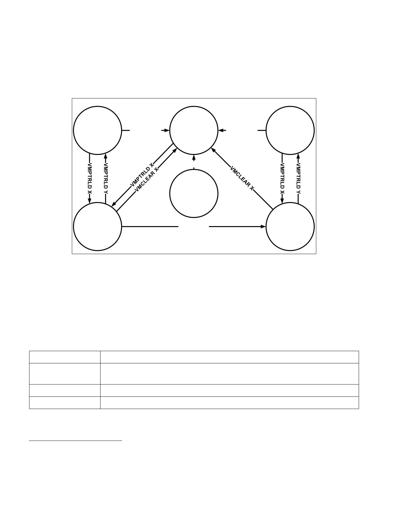
VIRTUAL MACHINE CONTROL STRUCTURES
Figure 25-1 illustrates the different states of a VMCS. It uses “X” to refer to the VMCS and “Y” to refer to any other
VMCS. Thus: “VMPTRLD X” always makes X current and active; “VMPTRLD Y” always makes X not current (because
it makes Y current); VMLAUNCH makes the launch state of X “launched” if X was current and its launch state was
“clear”; and VMCLEAR X always makes X inactive and not current and makes its launch state “clear”.
The figure does not illustrate operations that do not modify the VMCS state relative to these parameters (e.g.,
execution of VMPTRLD X when X is already current). Note that VMCLEAR X makes X “inactive, not current, and
clear,” even if X’s current state is not defined (e.g., even if X has not yet been initialized). See Section 25.11.3.
Active
Inactive
Active
Not Current
VMCLEAR X
Not Current
VMCLEAR X
Not Current
Clear
Clear
Launched
VMCLEAR X
Anything
Else
Active
Active
Current
VMLAUNCH
Current
Clear
Launched
Figure 25-1. States of VMCS X
Because a shadow VMCS (see Section 25.10) cannot be used for VM entry, the launch state of a shadow VMCS is
not meaningful. Figure 25-1 does not illustrate all the ways in which a shadow VMCS may be made active.
25.2
FORMAT OF THE VMCS REGION
A VMCS region comprises up to 4-KBytes.1 The format of a VMCS region is given in Table 25-1.
Table 25-1. Format of the VMCS Region
Byte Offset
Contents
0
Bits 30:0: VMCS revision identifier
Bit 31: shadow-VMCS indicator (see Section 25.10)
4
VMX-abort indicator
8
VMCS data (implementation-specific format)
1. The exact size is implementation specific and can be determined by consulting the VMX capability MSR IA32_VMX_BASIC to deter-
mine the size of the VMCS region (see Appendix A.1).
25-2
Vol. 3C
VIRTUAL MACHINE CONTROL STRUCTURES
The first 4 bytes of the VMCS region contain the VMCS revision identifier at bits 30:0.1 Processors that maintain
VMCS data in different formats (see below) use different VMCS revision identifiers. These identifiers enable soft-
ware to avoid using a VMCS region formatted for one processor on a processor that uses a different format.2 Bit 31
of this 4-byte region indicates whether the VMCS is a shadow VMCS (see Section 25.10).
Software should write the VMCS revision identifier to the VMCS region before using that region for a VMCS. The
VMCS revision identifier is never written by the processor; VMPTRLD fails if its operand references a VMCS region
whose VMCS revision identifier differs from that used by the processor. (VMPTRLD also fails if the shadow-VMCS
indicator is 1 and the processor does not support the 1-setting of the “VMCS shadowing” VM-execution control; see
Section 25.6.2) Software can discover the VMCS revision identifier that a processor uses by reading the VMX capa-
bility MSR IA32_VMX_BASIC (see Appendix A.1).
Software should clear or set the shadow-VMCS indicator depending on whether the VMCS is to be an ordinary
VMCS or a shadow VMCS (see Section 25.10). VMPTRLD fails if the shadow-VMCS indicator is set and the processor
does not support the 1-setting of the “VMCS shadowing” VM-execution control. Software can discover support for
this setting by reading the VMX capability MSR IA32_VMX_PROCBASED_CTLS2 (see Appendix A.3.3).
The next 4 bytes of the VMCS region are used for the VMX-abort indicator. The contents of these bits do not
control processor operation in any way. A logical processor writes a non-zero value into these bits if a VMX abort
occurs (see Section 28.7). Software may also write into this field.
The remainder of the VMCS region is used for VMCS data (those parts of the VMCS that control VMX non-root
operation and the VMX transitions). The format of these data is implementation-specific. VMCS data are discussed
in Section 25.3 through Section 25.9. To ensure proper behavior in VMX operation, software should maintain the
VMCS region and related structures (enumerated in Section 25.11.4) in writeback cacheable memory. Future
implementations may allow or require a different memory type3. Software should consult the VMX capability MSR
IA32_VMX_BASIC (see Appendix A.1).
25.3
ORGANIZATION OF VMCS DATA
The VMCS data are organized into six logical groups:
• Guest-state area. Processor state is saved into the guest-state area on VM exits and loaded from there on
VM entries.
• Host-state area. Processor state is loaded from the host-state area on VM exits.
• VM-execution control fields. These fields control processor behavior in VMX non-root operation. They
determine in part the causes of VM exits.
• VM-exit control fields. These fields control VM exits.
• VM-entry control fields. These fields control VM entries.
• VM-exit information fields. These fields receive information on VM exits and describe the cause and the
nature of VM exits. On some processors, these fields are read-only.4
The VM-execution control fields, the VM-exit control fields, and the VM-entry control fields are sometimes referred
to collectively as VMX controls.
1. Earlier versions of this manual specified that the VMCS revision identifier was a 32-bit field. For all processors produced prior to this
change, bit 31 of the VMCS revision identifier was 0.
2. Logical processors that use the same VMCS revision identifier use the same size for VMCS regions.
3. Alternatively, software may map any of these regions or structures with the UC memory type. Doing so is strongly discouraged
unless necessary as it will cause the performance of transitions using those structures to suffer significantly. In addition, the pro-
cessor will continue to use the memory type reported in the VMX capability MSR IA32_VMX_BASIC with exceptions noted in Appen-
dix A.1.
4. Software can discover whether these fields can be written by reading the VMX capability MSR IA32_VMX_MISC (see Appendix A.6).
Vol. 3C
25-3
VIRTUAL MACHINE CONTROL STRUCTURES
25.4
GUEST-STATE AREA
This section describes fields contained in the guest-state area of the VMCS. VM entries load processor state from
these fields and VM exits store processor state into these fields. See Section 27.3.2 and Section 28.3 for details.
25.4.1 Guest Register State
The following fields in the guest-state area correspond to processor registers:
• Control registers CR0, CR3, and CR4 (64 bits each; 32 bits on processors that do not support Intel 64 archi-
tecture).
• Debug register DR7 (64 bits; 32 bits on processors that do not support Intel 64 architecture).
• RSP, RIP, and RFLAGS (64 bits each; 32 bits on processors that do not support Intel 64 architecture).1
• The following fields for each of the registers CS, SS, DS, ES, FS, GS, LDTR, and TR:
- Selector (16 bits).
- Base address (64 bits; 32 bits on processors that do not support Intel 64 architecture). The base-address
fields for CS, SS, DS, and ES have only 32 architecturally-defined bits; nevertheless, the corresponding
VMCS fields have 64 bits on processors that support Intel 64 architecture.
- Segment limit (32 bits). The limit field is always a measure in bytes.
- Access rights (32 bits). The format of this field is given in Table 25-2 and detailed as follows:
• The low 16 bits correspond to bits 23:8 of the upper 32 bits of a 64-bit segment descriptor. While bits
19:16 of code-segment and data-segment descriptors correspond to the upper 4 bits of the segment
limit, the corresponding bits (bits 11:8) are reserved in this VMCS field.
• Bit 16 indicates an unusable segment. Attempts to use such a segment fault except in 64-bit mode.
In general, a segment register is unusable if it has been loaded with a null selector.2
• Bits 31:17 are reserved.
Table 25-2. Format of Access Rights
Bit Position(s)
Field
3:0
Segment type
4
S - Descriptor type (0 = system; 1 = code or data)
6:5
DPL - Descriptor privilege level
7
P - Segment present
11:8
Reserved
12
AVL - Available for use by system software
1. This chapter uses the notation RAX, RIP, RSP, RFLAGS, etc. for processor registers because most processors that support VMX oper-
ation also support Intel 64 architecture. For processors that do not support Intel 64 architecture, this notation refers to the 32-bit
forms of those registers (EAX, EIP, ESP, EFLAGS, etc.). In a few places, notation such as EAX is used to refer specifically to lower 32
bits of the indicated register.
2. There are a few exceptions to this statement. For example, a segment with a non-null selector may be unusable following a task
switch that fails after its commit point; see “Interrupt 10-Invalid TSS Exception (#TS)” in Section 6.14, “Exception and Interrupt
Handling in 64-bit Mode,” of the Intel® 64 and IA-32 Architectures Software Developer’s Manual, Volume 3A. In contrast, the TR reg-
ister is usable after processor reset despite having a null selector; see Table 11-1 in the Intel® 64 and IA-32 Architectures Software
Developer’s Manual, Volume 3A.
25-4
Vol. 3C
VIRTUAL MACHINE CONTROL STRUCTURES
Table 25-2. Format of Access Rights (Contd.)
Bit Position(s)
Field
13
Reserved (except for CS)
L - 64-bit mode active (for CS only)
14
D/B - Default operation size (0 = 16-bit segment; 1 = 32-bit segment)
15
G - Granularity
16
Segment unusable (0 = usable; 1 = unusable)
31:17
Reserved
The base address, segment limit, and access rights compose the “hidden” part (or “descriptor cache”) of each
segment register. These data are included in the VMCS because it is possible for a segment register’s descriptor
cache to be inconsistent with the segment descriptor in memory (in the GDT or the LDT) referenced by the
segment register’s selector.
The value of the DPL field for SS is always equal to the logical processor’s current privilege level (CPL).1
On some processors, executions of VMWRITE ignore attempts to write non-zero values to any of bits 11:8 or
bits 31:17. On such processors, VMREAD always returns 0 for those bits, and VM entry treats those bits as if
they were all 0 (see Section 27.3.1.2).
•
The following fields for each of the registers GDTR and IDTR:
- Base address (64 bits; 32 bits on processors that do not support Intel 64 architecture).
- Limit (32 bits). The limit fields contain 32 bits even though these fields are specified as only 16 bits in the
architecture.
•
The following MSRs:
- IA32_DEBUGCTL (64 bits)
- IA32_SYSENTER_CS (32 bits)
- IA32_SYSENTER_ESP and IA32_SYSENTER_EIP (64 bits; 32 bits on processors that do not support Intel 64
architecture)
- IA32_PERF_GLOBAL_CTRL (64 bits). This field is supported only on processors that support the 1-setting
of the “load IA32_PERF_GLOBAL_CTRL” VM-entry control.
- IA32_PAT (64 bits). This field is supported only on processors that support either the 1-setting of the “load
IA32_PAT” VM-entry control or that of the “save IA32_PAT” VM-exit control.
- IA32_EFER (64 bits). This field is supported only on processors that support either the 1-setting of the “load
IA32_EFER” VM-entry control or that of the “save IA32_EFER” VM-exit control.
- IA32_BNDCFGS (64 bits). This field is supported only on processors that support either the 1-setting of the
“load IA32_BNDCFGS” VM-entry control or that of the “clear IA32_BNDCFGS” VM-exit control.
- IA32_RTIT_CTL (64 bits). This field is supported only on processors that support either the 1-setting of the
“load IA32_RTIT_CTL” VM-entry control or that of the “clear IA32_RTIT_CTL” VM-exit control.
- IA32_LBR_CTL (64 bits). This field is supported only on processors that support either the 1-setting of the
“load guest IA32_LBR_CTL” VM-entry control or that of the “clear IA32_LBR_CTL” VM-exit control.
- IA32_S_CET (64 bits; 32 bits on processors that do not support Intel 64 architecture). This field is
supported only on processors that support the 1-setting of the “load CET state” VM-entry control.
- IA32_INTERRUPT_SSP_TABLE_ADDR (64 bits; 32 bits on processors that do not support Intel 64 archi-
tecture). This field is supported only on processors that support the 1-setting of the “load CET state” VM-
entry control.
1.
In protected mode, CPL is also associated with the RPL field in the CS selector. However, the RPL fields are not meaningful in real-
address mode or in virtual-8086 mode.
Vol. 3C
25-5
VIRTUAL MACHINE CONTROL STRUCTURES
- IA32_PKRS (64 bits). This field is supported only on processors that support the 1-setting of the “load
PKRS” VM-entry control.
• The shadow-stack pointer register SSP (64 bits; 32 bits on processors that do not support Intel 64 archi-
tecture). This field is supported only on processors that support the 1-setting of the “load CET state” VM-entry
control.
• The register SMBASE (32 bits). This register contains the base address of the logical processor’s SMRAM image.
25.4.2 Guest Non-Register State
In addition to the register state described in Section 25.4.1, the guest-state area includes the following fields that
characterize guest state but which do not correspond to processor registers:
• Activity state (32 bits). This field identifies the logical processor’s activity state. When a logical processor is
executing instructions normally, it is in the active state. Execution of certain instructions and the occurrence
of certain events may cause a logical processor to transition to an inactive state in which it ceases to execute
instructions.
The following activity states are defined:1
- 0: Active. The logical processor is executing instructions normally.
- 1: HLT. The logical processor is inactive because it executed the HLT instruction.
- 2: Shutdown. The logical processor is inactive because it incurred a triple fault2 or some other serious
error.
- 3: Wait-for-SIPI. The logical processor is inactive because it is waiting for a startup-IPI (SIPI).
Future processors may include support for other activity states. Software should read the VMX capability MSR
IA32_VMX_MISC (see Appendix A.6) to determine what activity states are supported.
• Interruptibility state (32 bits). The IA-32 architecture includes features that permit certain events to be
blocked for a period of time. This field contains information about such blocking. Details and the format of this
field are given in Table 25-3.
Table 25-3. Format of Interruptibility State
Bit
Bit Name
Notes
Position(s)
0
Blocking by STI
See the “STI-Set Interrupt Flag” section in Chapter 4 of the Intel® 64 and IA-32 Architectures
Software Developer’s Manual, Volume 2B.
Execution of STI with RFLAGS.IF = 0 blocks maskable interrupts on the instruction boundary
following its execution.1 Setting this bit indicates that this blocking is in effect.
1
Blocking by
See Section 6.8.3, “Masking Exceptions and Interrupts When Switching Stacks,” in the Intel® 64
MOV SS
and IA-32 Architectures Software Developer’s Manual, Volume 3A.
Execution of a MOV to SS or a POP to SS blocks or suppresses certain debug exceptions as well
as interrupts (maskable and nonmaskable) on the instruction boundary following its execution.
Setting this bit indicates that this blocking is in effect.2 This document uses the term “blocking
by MOV SS,” but it applies equally to POP SS.
2
Blocking by SMI
See Section 32.2, “System Management Interrupt (SMI).” System-management interrupts
(SMIs) are disabled while the processor is in system-management mode (SMM). Setting this bit
indicates that blocking of SMIs is in effect.
1. Execution of the MWAIT instruction may put a logical processor into an inactive state. However, this VMCS field never reflects this
state. See Section 28.1.
2. A triple fault occurs when a logical processor encounters an exception while attempting to deliver a double fault.
25-6
Vol. 3C

VIRTUAL MACHINE CONTROL STRUCTURES
Table 25-3. Format of Interruptibility State (Contd.)
Bit
Bit Name
Notes
Position(s)
3
Blocking by NMI
See Section 6.7.1, “Handling Multiple NMIs,” in the Intel® 64 and IA-32 Architectures Software
Developer’s Manual, Volume 3A and Section 32.8, “NMI Handling While in SMM.”
Delivery of a non-maskable interrupt (NMI) or a system-management interrupt (SMI) blocks
subsequent NMIs until the next execution of IRET. See Section 26.3 for how this behavior of
IRET may change in VMX non-root operation. Setting this bit indicates that blocking of NMIs is
in effect. Clearing this bit does not imply that NMIs are not (temporarily) blocked for other
reasons.
If the “virtual NMIs” VM-execution control (see Section 25.6.1) is 1, this bit does not control the
blocking of NMIs. Instead, it refers to “virtual-NMI blocking” (the fact that guest software is not
ready for an NMI).
4
Enclave
Set to 1 if the VM exit occurred while the logical processor was in enclave mode.
interruption
Such VM exits includes those caused by interrupts, non-maskable interrupts, system-
management interrupts, INIT signals, and exceptions occurring in enclave mode as well as
exceptions encountered during the delivery of such events incident to enclave mode.
A VM exit that is incident to delivery of an event injected by VM entry leaves this bit
unmodified.
31:5
Reserved
VM entry will fail if these bits are not 0. See Section 27.3.1.5.
NOTES:
1. Nonmaskable interrupts and system-management interrupts may also be inhibited on the instruction boundary following such an
execution of STI.
2. System-management interrupts may also be inhibited on the instruction boundary following such an execution of MOV or POP.
• Pending debug exceptions (64 bits; 32 bits on processors that do not support Intel 64 architecture). IA-32
processors may recognize one or more debug exceptions without immediately delivering them.1 This field
contains information about such exceptions. This field is described in Table 25-4.
Table 25-4. Format of Pending-Debug-Exceptions
Bit
Bit Name
Notes
Position(s)
3:0
B3 - B0
When set, each of these bits indicates that the corresponding breakpoint condition was met.
Any of these bits may be set even if the corresponding enabling bit in DR7 is not set.
10:4
Reserved
VM entry fails if these bits are not 0. See Section 27.3.1.5.
11
BLD
When set, this bit indicates that a bus lock was asserted while OS bus-lock detection was
enabled and CPL > 0 (see Section 18.3.1.6, “OS Bus-Lock Detection”).1
12
Enabled
When set, this bit indicates that at least one data or I/O breakpoint was met and was enabled in
breakpoint
DR7; the XBEGIN instruction was executed immediately before the VM exit and advanced
debugging of RTM transactional regions had been enabled; or a bus lock was asserted while
CPL > 0 and OS bus-lock detection had been enabled.
13
Reserved
VM entry fails if this bit is not 0. See Section 27.3.1.5.
1. For example, execution of a MOV to SS or a POP to SS may inhibit some debug exceptions for one instruction. See Section 6.8.3 of
Intel® 64 and IA-32 Architectures Software Developer’s Manual, Volume 3A. In addition, certain events incident to an instruction
(for example, an INIT signal) may take priority over debug traps generated by that instruction. See Table 6-2 in the Intel® 64 and
IA-32 Architectures Software Developer’s Manual, Volume 3A.
Vol. 3C
25-7
VIRTUAL MACHINE CONTROL STRUCTURES
Table 25-4. Format of Pending-Debug-Exceptions (Contd.)
Bit
Bit Name
Notes
Position(s)
14
BS
When set, this bit indicates that a debug exception would have been triggered by single-step
execution mode.
15
Reserved
VM entry fails if this bit is not 0. See Section 27.3.1.5.
16
RTM
When set, this bit indicates that a debug exception (#DB) or a breakpoint exception (#BP)
occurred inside an RTM region while advanced debugging of RTM transactional regions was
enabled (see Section 16.3.7, “RTM-Enabled Debugger Support,” of Intel® 64 and IA-32
Architectures Software Developer’s Manual, Volume 1).2
63:17
Reserved
VM entry fails if these bits are not 0. See Section 27.3.1.5. Bits 63:32 exist only on processors
that support Intel 64 architecture.
NOTES:
1. In general, the format of this field matches that of DR6. However, DR6 clears bit 11 to indicate detection of a bus lock, while this field
sets the bit to indicate that condition.
2. In general, the format of this field matches that of DR6. However, DR6 clears bit 16 to indicate an RTM-related exception, while this
field sets the bit to indicate that condition.
• VMCS link pointer (64 bits). If the “VMCS shadowing” VM-execution control is 1, the VMREAD and VMWRITE
instructions access the VMCS referenced by this pointer (see Section 25.10). Otherwise, software should set
this field to FFFFFFFF_FFFFFFFFH to avoid VM-entry failures (see Section 27.3.1.5).
• VMX-preemption timer value (32 bits). This field is supported only on processors that support the 1-setting
of the “activate VMX-preemption timer” VM-execution control. This field contains the value that the VMX-
preemption timer will use following the next VM entry with that setting. See Section 26.5.1 and Section 27.7.4.
• Page-directory-pointer-table entries (PDPTEs; 64 bits each). These four (4) fields (PDPTE0, PDPTE1,
PDPTE2, and PDPTE3) are supported only on processors that support the 1-setting of the “enable EPT” VM-
execution control. They correspond to the PDPTEs referenced by CR3 when PAE paging is in use (see Section
4.4 in the Intel® 64 and IA-32 Architectures Software Developer’s Manual, Volume 3A). They are used only if
the “enable EPT” VM-execution control is 1.
• Guest interrupt status (16 bits). This field is supported only on processors that support the 1-setting of the
“virtual-interrupt delivery” VM-execution control. It characterizes part of the guest’s virtual-APIC state and
does not correspond to any processor or APIC registers. It comprises two 8-bit subfields:
- Requesting virtual interrupt (RVI). This is the low byte of the guest interrupt status. The processor
treats this value as the vector of the highest priority virtual interrupt that is requesting service. (The value
0 implies that there is no such interrupt.)
- Servicing virtual interrupt (SVI). This is the high byte of the guest interrupt status. The processor treats
this value as the vector of the highest priority virtual interrupt that is in service. (The value 0 implies that
there is no such interrupt.)
See Chapter 30 for more information on the use of this field.
• PML index (16 bits). This field is supported only on processors that support the 1-setting of the “enable PML”
VM-execution control. It contains the logical index of the next entry in the page-modification log. Because the
page-modification log comprises 512 entries, the PML index is typically a value in the range 0-511. Details of
the page-modification log and use of the PML index are given in Section 29.3.6.
25.5
HOST-STATE AREA
This section describes fields contained in the host-state area of the VMCS. As noted earlier, processor state is
loaded from these fields on every VM exit (see Section 28.5).
All fields in the host-state area correspond to processor registers:
25-8
Vol. 3C
VIRTUAL MACHINE CONTROL STRUCTURES
• CR0, CR3, and CR4 (64 bits each; 32 bits on processors that do not support Intel 64 architecture).
• RSP and RIP (64 bits each; 32 bits on processors that do not support Intel 64 architecture).
• Selector fields (16 bits each) for the segment registers CS, SS, DS, ES, FS, GS, and TR. There is no field in the
host-state area for the LDTR selector.
• Base-address fields for FS, GS, TR, GDTR, and IDTR (64 bits each; 32 bits on processors that do not support
Intel 64 architecture).
• The following MSRs:
- IA32_SYSENTER_CS (32 bits)
- IA32_SYSENTER_ESP and IA32_SYSENTER_EIP (64 bits; 32 bits on processors that do not support Intel 64
architecture).
- IA32_PERF_GLOBAL_CTRL (64 bits). This field is supported only on processors that support the 1-setting
of the “load IA32_PERF_GLOBAL_CTRL” VM-exit control.
- IA32_PAT (64 bits). This field is supported only on processors that support the 1-setting of the “load
IA32_PAT” VM-exit control.
- IA32_EFER (64 bits). This field is supported only on processors that support the 1-setting of the “load
IA32_EFER” VM-exit control.
- IA32_S_CET (64 bits; 32 bits on processors that do not support Intel 64 architecture). This field is
supported only on processors that support the 1-setting of the “load CET state” VM-exit control.
- IA32_INTERRUPT_SSP_TABLE_ADDR (64 bits; 32 bits on processors that do not support Intel 64 archi-
tecture). This field is supported only on processors that support the 1-setting of the “load CET state” VM-
exit control.
- IA32_PKRS (64 bits). This field is supported only on processors that support the 1-setting of the “load
PKRS” VM-exit control.
• The shadow-stack pointer register SSP (64 bits; 32 bits on processors that do not support Intel 64 archi-
tecture). This field is supported only on processors that support the 1-setting of the “load CET state” VM-exit
control.
In addition to the state identified here, some processor state components are loaded with fixed values on every
VM exit; there are no fields corresponding to these components in the host-state area. See Section 28.5 for details
of how state is loaded on VM exits.
25.6
VM-EXECUTION CONTROL FIELDS
The VM-execution control fields govern VMX non-root operation. These are described in Section 25.6.1 through
Section 25.6.8.
25.6.1 Pin-Based VM-Execution Controls
The pin-based VM-execution controls constitute a 32-bit vector that governs the handling of asynchronous events
(for example: interrupts).1 Table 25-5 lists the controls. See Chapter 28 for how these controls affect processor
behavior in VMX non-root operation.
1. Some asynchronous events cause VM exits regardless of the settings of the pin-based VM-execution controls (see Section 26.2).
Vol. 3C
25-9

VIRTUAL MACHINE CONTROL STRUCTURES
Table 25-5. Definitions of Pin-Based VM-Execution Controls
Bit Position(s)
Name
Description
0
External-interrupt
If this control is 1, external interrupts cause VM exits. Otherwise, they are delivered normally
exiting
through the guest interrupt-descriptor table (IDT). If this control is 1, the value of RFLAGS.IF
does not affect interrupt blocking.
3
NMI exiting
If this control is 1, non-maskable interrupts (NMIs) cause VM exits. Otherwise, they are
delivered normally using descriptor 2 of the IDT. This control also determines interactions
between IRET and blocking by NMI (see Section 26.3).
5
Virtual NMIs
If this control is 1, NMIs are never blocked and the “blocking by NMI” bit (bit 3) in the
interruptibility-state field indicates “virtual-NMI blocking” (see Table 25-3). This control also
interacts with the “NMI-window exiting” VM-execution control (see Section 25.6.2).
6
Activate VMX-
If this control is 1, the VMX-preemption timer counts down in VMX non-root operation; see
preemption timer
Section 26.5.1. A VM exit occurs when the timer counts down to zero; see Section 26.2.
7
Process posted
If this control is 1, the processor treats interrupts with the posted-interrupt notification vector
interrupts
(see Section 25.6.8) specially, updating the virtual-APIC page with posted-interrupt requests
(see Section 30.6).
All other bits in this field are reserved, some to 0 and some to 1. Software should consult the VMX capability MSRs
IA32_VMX_PINBASED_CTLS and IA32_VMX_TRUE_PINBASED_CTLS (see Appendix A.3.1) to determine how to set
reserved bits. Failure to set reserved bits properly causes subsequent VM entries to fail (see Section 27.2.1.1).
The first processors to support the virtual-machine extensions supported only the 1-settings of bits 1, 2, and 4. The
VMX capability MSR IA32_VMX_PINBASED_CTLS will always report that these bits must be 1. Logical processors
that support the 0-settings of any of these bits will support the VMX capability MSR IA32_VMX_TRUE_PIN-
BASED_CTLS MSR, and software should consult this MSR to discover support for the 0-settings of these bits. Soft-
ware that is not aware of the functionality of any one of these bits should set that bit to 1.
25.6.2 Processor-Based VM-Execution Controls
The processor-based VM-execution controls constitute three vectors that govern the handling of synchronous
events, mainly those caused by the execution of specific instructions.1 These are the primary processor-based
VM-execution controls (32 bits), the secondary processor-based VM-execution controls (32 bits), and the
tertiary VM-execution controls (64 bits).
Table 25-6 lists the primary processor-based VM-execution controls. See Chapter 26 for more details of how these
controls affect processor behavior in VMX non-root operation.
Table 25-6. Definitions of Primary Processor-Based VM-Execution Controls
Bit Position(s)
Name
Description
2
Interrupt-window
If this control is 1, a VM exit occurs at the beginning of any instruction if RFLAGS.IF = 1 and
exiting
there are no other blocking of interrupts (see Section 25.4.2).
3
Use TSC offsetting
This control determines whether executions of RDTSC, executions of RDTSCP, and executions
of RDMSR that read from the IA32_TIME_STAMP_COUNTER MSR return a value modified by
the TSC offset field (see Section 25.6.5 and Section 26.3).
7
HLT exiting
This control determines whether executions of HLT cause VM exits.
9
INVLPG exiting
This determines whether executions of INVLPG cause VM exits.
10
MWAIT exiting
This control determines whether executions of MWAIT cause VM exits.
11
RDPMC exiting
This control determines whether executions of RDPMC cause VM exits.
1. Some instructions cause VM exits regardless of the settings of the processor-based VM-execution controls (see Section 26.1.2), as
do task switches (see Section 26.2).
25-10
Vol. 3C

VIRTUAL MACHINE CONTROL STRUCTURES
Table 25-6. Definitions of Primary Processor-Based VM-Execution Controls (Contd.)
Bit Position(s)
Name
Description
12
RDTSC exiting
This control determines whether executions of RDTSC and RDTSCP cause VM exits.
15
CR3-load exiting
In conjunction with the CR3-target controls (see Section 25.6.7), this control determines
whether executions of MOV to CR3 cause VM exits. See Section 26.1.3.
The first processors to support the virtual-machine extensions supported only the 1-setting
of this control.
16
CR3-store exiting
This control determines whether executions of MOV from CR3 cause VM exits.
The first processors to support the virtual-machine extensions supported only the 1-setting
of this control.
17
Activate tertiary
This control determines whether the tertiary processor-based VM-execution controls are
controls
used. If this control is 0, the logical processor operates as if all the tertiary processor-based
VM-execution controls were also 0.
19
CR8-load exiting
This control determines whether executions of MOV to CR8 cause VM exits.
20
CR8-store exiting
This control determines whether executions of MOV from CR8 cause VM exits.
21
Use TPR shadow
Setting this control to 1 enables TPR virtualization and other APIC-virtualization features. See
Chapter 30.
22
NMI-window
If this control is 1, a VM exit occurs at the beginning of any instruction if there is no virtual-
exiting
NMI blocking (see Section 25.4.2).
23
MOV-DR exiting
This control determines whether executions of MOV DR cause VM exits.
24
Unconditional I/O
This control determines whether executions of I/O instructions (IN, INS/INSB/INSW/INSD, OUT,
exiting
and OUTS/OUTSB/OUTSW/OUTSD) cause VM exits.
25
Use I/O bitmaps
This control determines whether I/O bitmaps are used to restrict executions of I/O instructions
(see Section 25.6.4 and Section 26.1.3).
For this control, “0” means “do not use I/O bitmaps” and “1” means “use I/O bitmaps.” If the I/O
bitmaps are used, the setting of the “unconditional I/O exiting” control is ignored.
27
Monitor trap flag
If this control is 1, the monitor trap flag debugging feature is enabled. See Section 26.5.2.
28
Use MSR bitmaps
This control determines whether MSR bitmaps are used to control execution of the RDMSR
and WRMSR instructions (see Section 25.6.9 and Section 26.1.3).
For this control, “0” means “do not use MSR bitmaps” and “1” means “use MSR bitmaps.” If the
MSR bitmaps are not used, all executions of the RDMSR and WRMSR instructions cause
VM exits.
29
MONITOR exiting
This control determines whether executions of MONITOR cause VM exits.
30
PAUSE exiting
This control determines whether executions of PAUSE cause VM exits.
31
Activate secondary
This control determines whether the secondary processor-based VM-execution controls are
controls
used. If this control is 0, the logical processor operates as if all the secondary processor-based
VM-execution controls were also 0.
All other bits in this field are reserved, some to 0 and some to 1. Software should consult the VMX capability MSRs
IA32_VMX_PROCBASED_CTLS and IA32_VMX_TRUE_PROCBASED_CTLS (see Appendix A.3.2) to determine how
to set reserved bits. Failure to set reserved bits properly causes subsequent VM entries to fail (see Section
27.2.1.1).
The first processors to support the virtual-machine extensions supported only the 1-settings of bits 1, 4-6, 8, 13-
16, and 26. The VMX capability MSR IA32_VMX_PROCBASED_CTLS will always report that these bits must be 1.
Logical processors that support the 0-settings of any of these bits will support the VMX capability MSR IA32_VMX-
_TRUE_PROCBASED_CTLS MSR, and software should consult this MSR to discover support for the 0-settings of
these bits. Software that is not aware of the functionality of any one of these bits should set that bit to 1.
Bit 31 of the primary processor-based VM-execution controls determines whether the secondary processor-based
VM-execution controls are used. If that bit is 0, VM entry and VMX non-root operation function as if all the
secondary processor-based VM-execution controls were 0. Processors that support only the 0-setting of bit 31 of
Vol. 3C
25-11

VIRTUAL MACHINE CONTROL STRUCTURES
the primary processor-based VM-execution controls do not support the secondary processor-based VM-execution
controls.
Table 25-7 lists the secondary processor-based VM-execution controls. See Chapter 26 for more details of how
these controls affect processor behavior in VMX non-root operation.
Table 25-7. Definitions of Secondary Processor-Based VM-Execution Controls
Bit Position(s)
Name
Description
0
Virtualize APIC
If this control is 1, the logical processor treats specially accesses to the page with the APIC-
accesses
access address. See Section 30.4.
1
Enable EPT
If this control is 1, extended page tables (EPT) are enabled. See Section 29.3.
2
Descriptor-table
This control determines whether executions of LGDT, LIDT, LLDT, LTR, SGDT, SIDT, SLDT, and
exiting
STR cause VM exits.
3
Enable RDTSCP
If this control is 0, any execution of RDTSCP causes an invalid-opcode exception (#UD).
4
Virtualize x2APIC
If this control is 1, the logical processor treats specially RDMSR and WRMSR to APIC MSRs (in
mode
the range 800H-8FFH). See Section 30.5.
5
Enable VPID
If this control is 1, cached translations of linear addresses are associated with a virtual-
processor identifier (VPID). See Section 29.1.
6
WBINVD exiting
This control determines whether executions of WBINVD and WBNOINVD cause VM exits.
7
Unrestricted guest
This control determines whether guest software may run in unpaged protected mode or in real-
address mode.
8
APIC-register
If this control is 1, the logical processor virtualizes certain APIC accesses. See Section 30.4 and
virtualization
Section 30.5.
9
Virtual-interrupt
This controls enables the evaluation and delivery of pending virtual interrupts as well as the
delivery
emulation of writes to the APIC registers that control interrupt prioritization.
10
PAUSE-loop exiting
This control determines whether a series of executions of PAUSE can cause a VM exit (see
Section 25.6.13 and Section 26.1.3).
11
RDRAND exiting
This control determines whether executions of RDRAND cause VM exits.
12
Enable INVPCID
If this control is 0, any execution of INVPCID causes a #UD.
13
Enable
Setting this control to 1 enables use of the VMFUNC instruction in VMX non-root operation. See
VM functions
Section 26.5.6.
14
VMCS shadowing
If this control is 1, executions of VMREAD and VMWRITE in VMX non-root operation may access
a shadow VMCS (instead of causing VM exits). See Section 25.10 and Section 31.3.
15
Enable ENCLS
If this control is 1, executions of ENCLS consult the ENCLS-exiting bitmap to determine whether
exiting
the instruction causes a VM exit. See Section 25.6.16 and Section 26.1.3.
16
RDSEED exiting
This control determines whether executions of RDSEED cause VM exits.
17
Enable PML
If this control is 1, an access to a guest-physical address that sets an EPT dirty bit first adds an
entry to the page-modification log. See Section 29.3.6.
18
EPT-violation #VE
If this control is 1, EPT violations may cause virtualization exceptions (#VE) instead of VM exits.
See Section 26.5.7.
19
Conceal VMX from
If this control is 1, Intel Processor Trace suppresses from PIPs an indication that the processor
PT
was in VMX non-root operation and omits a VMCS packet from any PSB+ produced in VMX non-
root operation (see Chapter 33).
20
Enable
If this control is 0, any execution of XSAVES or XRSTORS causes a #UD.
XSAVES/XRSTORS
21
PASID translation
If this control is 1, PASID translation is performed for executions of ENQCMD and ENQCMDS. See
Section 26.5.8.
22
Mode-based
If this control is 1, EPT execute permissions are based on whether the linear address being
execute control for
accessed is supervisor mode or user mode. See Chapter 29.
EPT
25-12
Vol. 3C

VIRTUAL MACHINE CONTROL STRUCTURES
Table 25-7. Definitions of Secondary Processor-Based VM-Execution Controls (Contd.)
Bit Position(s)
Name
Description
23
Sub-page write
If this control is 1, EPT write permissions may be specified at the granularity of 128 bytes. See
permissions for
Section 29.3.4.
EPT
24
Intel PT uses guest
If this control is 1, all output addresses used by Intel Processor Trace are treated as guest-
physical addresses
physical addresses and translated using EPT. See Section 26.5.4.
25
Use TSC scaling
This control determines whether executions of RDTSC, executions of RDTSCP, and executions
of RDMSR that read from the IA32_TIME_STAMP_COUNTER MSR return a value modified by the
TSC multiplier field (see Section 25.6.5 and Section 26.3).
26
Enable user wait
If this control is 0, any execution of TPAUSE, UMONITOR, or UMWAIT causes a #UD.
and pause
27
Enable PCONFIG
If this control is 0, any execution of PCONFIG causes a #UD.
28
Enable ENCLV
If this control is 1, executions of ENCLV consult the ENCLV-exiting bitmap to determine whether
exiting
the instruction causes a VM exit. See Section 25.6.17 and Section 26.1.3.
30
VMM bus-lock
This control determines whether assertion of a bus lock causes a VM exit. See Section 26.2.
detection
31
Instruction timeout
If this control is 1, a VM exit occurs if certain operations prevent the processor from reaching an
instruction boundary within a specified amount of time. See Section 25.6.25 and Section 26.2.
All other bits in this field are reserved to 0. Software should consult the VMX capability MSR IA32_VMX_PROC-
BASED_CTLS2 (see Appendix A.3.3) to determine which bits may be set to 1. Failure to clear reserved bits causes
subsequent VM entries to fail (see Section 27.2.1.1).
Bit 17 of the primary processor-based VM-execution controls determines whether the tertiary processor-based
VM-execution controls are used. If that bit is 0, VM entry and VMX non-root operation function as if all the tertiary
processor-based VM-execution controls were 0. Processors that support only the 0-setting of bit 17 of the primary
processor-based VM-execution controls do not support the tertiary processor-based VM-execution controls.
Table 25-8 lists the tertiary processor-based VM-execution controls. See Chapter 26 for more details of how these
controls affect processor behavior in VMX non-root operation.
Table 25-8. Definitions of Tertiary Processor-Based VM-Execution Controls
Bit Position(s)
Name
Description
0
LOADIWKEY exiting
This control determines whether executions of LOADIWKEY cause VM exits.
1
Enable HLAT
This control enables hypervisor-managed linear-address translation. See Section 4.5.1.
2
EPT paging-write
If this control is 1, EPT permissions can be specified to allow writes only for paging-related
control
updates. See Section 29.3.3.2.
3
Guest-paging
If this control is 1, EPT permissions can be specified to prevent accesses using linear addresses
verification
whose translation has certain properties. See Section 29.3.3.2.
4
IPI virtualization
If this control is 1, virtualization of interprocessor interrupts (IPIs) is enabled. See Section
30.1.6.
7
Virtualize
If this control is 1, the operation of the RDMSR and WRMSR instructions is changed when
IA32_SPEC_CTRL
accessing the IA32_SPEC_CTRL MSR. See Section 26.3.
All other bits in this field are reserved to 0. Software should consult the VMX capability MSR IA32_VMX_PROC-
BASED_CTLS3 (see Appendix A.3.4) to determine which bits may be set to 1. Failure to clear reserved bits causes
subsequent VM entries to fail (see Section 27.2.1.1).
Vol. 3C
25-13
VIRTUAL MACHINE CONTROL STRUCTURES
25.6.3 Exception Bitmap
The exception bitmap is a 32-bit field that contains one bit for each exception. When an exception occurs, its
vector is used to select a bit in this field. If the bit is 1, the exception causes a VM exit. If the bit is 0, the exception
is delivered normally through the IDT, using the descriptor corresponding to the exception’s vector.
Whether a page fault (exception with vector 14) causes a VM exit is determined by bit 14 in the exception bitmap
as well as the error code produced by the page fault and two 32-bit fields in the VMCS (the page-fault error-code
mask and page-fault error-code match). See Section 26.2 for details.
25.6.4 I/O-Bitmap Addresses
The VM-execution control fields include the 64-bit physical addresses of I/O bitmaps A and B (each of which are
4 KBytes in size). I/O bitmap A contains one bit for each I/O port in the range 0000H through 7FFFH; I/O bitmap B
contains bits for ports in the range 8000H through FFFFH.
A logical processor uses these bitmaps if and only if the “use I/O bitmaps” control is 1. If the bitmaps are used,
execution of an I/O instruction causes a VM exit if any bit in the I/O bitmaps corresponding to a port it accesses is
1. See Section 26.1.3 for details. If the bitmaps are used, their addresses must be 4-KByte aligned.
25.6.5 Time-Stamp Counter Offset and Multiplier
The VM-execution control fields include a 64-bit TSC-offset field. If the “RDTSC exiting” control is 0 and the “use
TSC offsetting” control is 1, this field controls executions of the RDTSC and RDTSCP instructions. It also controls
executions of the RDMSR instruction that read from the IA32_TIME_STAMP_COUNTER MSR. For all of these, the
value of the TSC offset is added to the value of the time-stamp counter, and the sum is returned to guest software
in EDX:EAX.
Processors that support the 1-setting of the “use TSC scaling” control also support a 64-bit TSC-multiplier field.
If this control is 1 (and the “RDTSC exiting” control is 0 and the “use TSC offsetting” control is 1), this field also
affects the executions of the RDTSC, RDTSCP, and RDMSR instructions identified above. Specifically, the contents
of the time-stamp counter is first multiplied by the TSC multiplier before adding the TSC offset.
See Chapter 26 for a detailed treatment of the behavior of RDTSC, RDTSCP, and RDMSR in VMX non-root operation.
25.6.6 Guest/Host Masks and Read Shadows for CR0 and CR4
VM-execution control fields include guest/host masks and read shadows for the CR0 and CR4 registers. These
fields control executions of instructions that access those registers (including CLTS, LMSW, MOV CR, and SMSW).
They are 64 bits on processors that support Intel 64 architecture and 32 bits on processors that do not.
In general, bits set to 1 in a guest/host mask correspond to bits “owned” by the host:
• Guest attempts to set them (using CLTS, LMSW, or MOV to CR) to values differing from the corresponding bits
in the corresponding read shadow cause VM exits.
• Guest reads (using MOV from CR or SMSW) return values for these bits from the corresponding read shadow.
Bits cleared to 0 correspond to bits “owned” by the guest; guest attempts to modify them succeed and guest reads
return values for these bits from the control register itself.
See Chapter 28 for details regarding how these fields affect VMX non-root operation.
25.6.7 CR3-Target Controls
The VM-execution control fields include a set of 4 CR3-target values and a CR3-target count. The CR3-target
values each have 64 bits on processors that support Intel 64 architecture and 32 bits on processors that do not. The
CR3-target count has 32 bits on all processors.
25-14
Vol. 3C
VIRTUAL MACHINE CONTROL STRUCTURES
An execution of MOV to CR3 in VMX non-root operation does not cause a VM exit if its source operand matches one
of these values. If the CR3-target count is n, only the first n CR3-target values are considered; if the CR3-target
count is 0, MOV to CR3 always causes a VM exit.
There are no limitations on the values that can be written for the CR3-target values. VM entry fails (see Section
27.2) if the CR3-target count is greater than 4.
Future processors may support a different number of CR3-target values. Software should read the VMX capability
MSR IA32_VMX_MISC (see Appendix A.6) to determine the number of values supported.
25.6.8 Controls for APIC Virtualization
There are three mechanisms by which software accesses registers of the logical processor’s local APIC:
• If the local APIC is in xAPIC mode, it can perform memory-mapped accesses to addresses in the 4-KByte page
referenced by the physical address in the IA32_APIC_BASE MSR (see Section 11.4.4, “Local APIC Status and
Location,” in the Intel® 64 and IA-32 Architectures Software Developer’s Manual, Volume 3A, and the Intel® 64
Architecture Processor Topology Enumeration Technical Paper).1
• If the local APIC is in x2APIC mode, it can accesses the local APIC’s registers using the RDMSR and WRMSR
instructions (see the Intel® 64 Architecture Processor Topology Enumeration Technical Paper).
• In 64-bit mode, it can access the local APIC’s task-priority register (TPR) using the MOV CR8 instruction.
Several processor-based VM-execution controls (see Section 25.6.2) control such accesses. These are “use TPR
shadow”, “virtualize APIC accesses”, “virtualize x2APIC mode”, “virtual-interrupt delivery”, “APIC-register virtual-
ization”, and “IPI virtualization”. These controls interact with the following fields:
•
APIC-access address (64 bits). This field contains the physical address of the 4-KByte APIC-access page.
If the “virtualize APIC accesses” VM-execution control is 1, access to this page may cause VM exits or be
virtualized by the processor. See Section 30.4.
The APIC-access address exists only on processors that support the 1-setting of the “virtualize APIC accesses”
VM-execution control.
•
Virtual-APIC address (64 bits). This field contains the physical address of the 4-KByte virtual-APIC page.
The processor uses the virtual-APIC page to virtualize certain accesses to APIC registers and to manage virtual
interrupts; see Chapter 30.
Depending on the setting of the controls indicated earlier, the virtual-APIC page may be accessed by the
following operations:
- The MOV CR8 instructions (see Section 30.3).
- Accesses to the APIC-access page if, in addition, the “virtualize APIC accesses” VM-execution control is 1
(see Section 30.4).
- The RDMSR and WRMSR instructions if, in addition, the value of ECX is in the range 800H-8FFH (indicating
an APIC MSR) and the “virtualize x2APIC mode” VM-execution control is 1 (see Section 30.5).
If the “use TPR shadow” VM-execution control is 1, VM entry ensures that the virtual-APIC address is 4-KByte
aligned. The virtual-APIC address exists only on processors that support the 1-setting of the “use TPR shadow”
VM-execution control.
•
TPR threshold (32 bits). Bits 3:0 of this field determine the threshold below which bits 7:4 of VTPR (see
Section 30.1.1) cannot fall. If the “virtual-interrupt delivery” VM-execution control is 0, a VM exit occurs after
an operation (e.g., an execution of MOV to CR8) that reduces the value of those bits below the TPR threshold.
See Section 30.1.2.
The TPR threshold exists only on processors that support the 1-setting of the “use TPR shadow” VM-execution
control.
•
EOI-exit bitmap (4 fields; 64 bits each). These fields are supported only on processors that support the 1-
setting of the “virtual-interrupt delivery” VM-execution control. They are used to determine which virtualized
writes to the APIC’s EOI register cause VM exits:
1.
If the local APIC does not support x2APIC mode, it is always in xAPIC mode.
Vol. 3C
25-15
VIRTUAL MACHINE CONTROL STRUCTURES
- EOI_EXIT0 contains bits for vectors from 0 (bit 0) to 63 (bit 63).
- EOI_EXIT1 contains bits for vectors from 64 (bit 0) to 127 (bit 63).
- EOI_EXIT2 contains bits for vectors from 128 (bit 0) to 191 (bit 63).
- EOI_EXIT3 contains bits for vectors from 192 (bit 0) to 255 (bit 63).
See Section 30.1.4 for more information on the use of this field.
• Posted-interrupt notification vector (16 bits). This field is supported only on processors that support the 1-
setting of the “process posted interrupts” VM-execution control. Its low 8 bits contain the interrupt vector that
is used to notify a logical processor that virtual interrupts have been posted. See Section 30.6 for more
information on the use of this field.
• Posted-interrupt descriptor address (64 bits). This field is supported only on processors that support the 1-
setting of the “process posted interrupts” VM-execution control. It is the physical address of a 64-byte aligned
posted interrupt descriptor. See Section 30.6 for more information on the use of this field.
• PID-pointer table address (64 bits). This field contains the physical address of the PID-pointer table. If the
“IPI virtualization” VM-execution control is 1, the logical processor uses entries in this table to virtualize IPIs.
See Section 30.1.6.
• Last PID-pointer index (16 bits). This field contains the index of the last entry in the PID-pointer table.
25.6.9 MSR-Bitmap Address
On processors that support the 1-setting of the “use MSR bitmaps” VM-execution control, the VM-execution control
fields include the 64-bit physical address of four contiguous MSR bitmaps, which are each 1-KByte in size. This
field does not exist on processors that do not support the 1-setting of that control. The four bitmaps are:
• Read bitmap for low MSRs (located at the MSR-bitmap address). This contains one bit for each MSR address
in the range 00000000H to 00001FFFH. The bit determines whether an execution of RDMSR applied to that
MSR causes a VM exit.
• Read bitmap for high MSRs (located at the MSR-bitmap address plus 1024). This contains one bit for each
MSR address in the range C0000000H toC0001FFFH. The bit determines whether an execution of RDMSR
applied to that MSR causes a VM exit.
• Write bitmap for low MSRs (located at the MSR-bitmap address plus 2048). This contains one bit for each
MSR address in the range 00000000H to 00001FFFH. The bit determines whether an execution of WRMSR
applied to that MSR causes a VM exit.
• Write bitmap for high MSRs (located at the MSR-bitmap address plus 3072). This contains one bit for each
MSR address in the range C0000000H toC0001FFFH. The bit determines whether an execution of WRMSR
applied to that MSR causes a VM exit.
A logical processor uses these bitmaps if and only if the “use MSR bitmaps” control is 1. If the bitmaps are used, an
execution of RDMSR or WRMSR causes a VM exit if the value of RCX is in neither of the ranges covered by the
bitmaps or if the appropriate bit in the MSR bitmaps (corresponding to the instruction and the RCX value) is 1. See
Section 26.1.3 for details. If the bitmaps are used, their address must be 4-KByte aligned.
25.6.10 Executive-VMCS Pointer
The executive-VMCS pointer is a 64-bit field used in the dual-monitor treatment of system-management interrupts
(SMIs) and system-management mode (SMM). SMM VM exits save this field as described in Section 32.15.2.
VM entries that return from SMM use this field as described in Section 32.15.4.
25-16
Vol. 3C
VIRTUAL MACHINE CONTROL STRUCTURES
25.6.11 Extended-Page-Table Pointer (EPTP)
The extended-page-table pointer (EPTP) contains the address of the base of EPT PML4 table (see Section
29.3.2), as well as other EPT configuration information. The format of this field is shown in Table 25-9.
Table 25-9. Format of Extended-Page-Table Pointer
Bit
Field
Position(s)
2:0
EPT paging-structure memory type (see Section 29.3.7):
0 = Uncacheable (UC)
6 = Write-back (WB)
Other values are reserved.1
5:3
This value is 1 less than the EPT page-walk length (see Section 29.3.2)
6
Setting this control to 1 enables accessed and dirty flags for EPT (see Section 29.3.5)2
7
Setting this control to 1 enables enforcement of access rights for supervisor shadow-stack pages (see Section
29.3.3.2)3
11:8
Reserved
N-1:12
Bits N-1:12 of the physical address of the 4-KByte aligned EPT paging-structure (an EPT PML4 table with 4-level
EPT and an EPT PML5 table with 5-level EPT)4
63:N
Reserved
NOTES:
1. Software should read the VMX capability MSR IA32_VMX_EPT_VPID_CAP (see Appendix A.10) to determine what EPT paging-struc-
ture memory types are supported.
2. Not all processors support accessed and dirty flags for EPT. Software should read the VMX capability MSR IA32_VMX_EPT_VPID_-
CAP (see Appendix A.10) to determine whether the processor supports this feature.
3. Not all processors enforce access rights for shadow-stack pages. Software should read the VMX capability MSR IA32_VMX-
_EPT_VPID_CAP (see Appendix A.10) to determine whether the processor supports this feature.
4. N is the physical-address width supported by the logical processor. Software can determine a processor’s physical-address width by
executing CPUID with 80000008H in EAX. The physical-address width is returned in bits 7:0 of EAX.
The EPTP exists only on processors that support the 1-setting of the “enable EPT” VM-execution control.
25.6.12 Virtual-Processor Identifier (VPID)
The virtual-processor identifier (VPID) is a 16-bit field. It exists only on processors that support the 1-setting
of the “enable VPID” VM-execution control. See Section 29.1 for details regarding the use of this field.
25.6.13 Controls for PAUSE-Loop Exiting
On processors that support the 1-setting of the “PAUSE-loop exiting” VM-execution control, the VM-execution
control fields include the following 32-bit fields:
• PLE_Gap. Software can configure this field as an upper bound on the amount of time between two successive
executions of PAUSE in a loop.
• PLE_Window. Software can configure this field as an upper bound on the amount of time a guest is allowed to
execute in a PAUSE loop.
These fields measure time based on a counter that runs at the same rate as the timestamp counter (TSC). See
Section 26.1.3 for more details regarding PAUSE-loop exiting.
Vol. 3C
25-17
VIRTUAL MACHINE CONTROL STRUCTURES
25.6.14 VM-Function Controls
The VM-function controls constitute a 64-bit vector that governs use of the VMFUNC instruction in VMX non-root
operation. This field is supported only on processors that support the 1-settings of both the “activate secondary
controls” primary processor-based VM-execution control and the “enable VM functions” secondary processor-
based VM-execution control.
Table 25-10 lists the VM-function controls. See Section 26.5.6 for more details of how these controls affect
processor behavior in VMX non-root operation.
Table 25-10. Definitions of VM-Function Controls
Bit Position(s)
Name
Description
0
EPTP switching
The EPTP-switching VM function changes the EPT pointer to a value chosen from the EPTP list.
See Section 26.5.6.3.
All other bits in this field are reserved to 0. Software should consult the VMX capability MSR IA32_VMX_VMFUNC
(see Appendix A.11) to determine which bits are reserved. Failure to clear reserved bits causes subsequent
VM entries to fail (see Section 27.2.1.1).
Processors that support the 1-setting of the “EPTP switching” VM-function control also support a 64-bit field called
the EPTP-list address. This field contains the physical address of the 4-KByte EPTP list. The EPTP list comprises
512 8-Byte entries (each an EPTP value) and is used by the EPTP-switching VM function (see Section 26.5.6.3).
25.6.15 VMCS Shadowing Bitmap Addresses
On processors that support the 1-setting of the “VMCS shadowing” VM-execution control, the VM-execution control
fields include the 64-bit physical addresses of the VMREAD bitmap and the VMWRITE bitmap. Each bitmap is 4
KBytes in size and thus contains 32 KBits. The addresses are the VMREAD-bitmap address and the VMWRITE-
bitmap address.
If the “VMCS shadowing” VM-execution control is 1, executions of VMREAD and VMWRITE may consult these
bitmaps (see Section 25.10 and Section 31.3).
25.6.16 ENCLS-Exiting Bitmap
The ENCLS-exiting bitmap is a 64-bit field. If the “enable ENCLS exiting” VM-execution control is 1, execution of
ENCLS causes a VM exit if the bit in this field corresponding to the value of EAX is 1. If the bit is 0, the instruction
executes normally. See Section 26.1.3 for more information.
25.6.17 ENCLV-Exiting Bitmap
The ENCLV-exiting bitmap is a 64-bit field. If the “enable ENCLV exiting” VM-execution control is 1, execution of
ENCLV causes a VM exit if the bit in this field corresponding to the value of EAX is 1. If the bit is 0, the instruction
executes normally. See Section 26.1.3 for more information.
25.6.18 PCONFIG-Exiting Bitmap
The PCONFIG-exiting bitmap is a 64-bit field. If the “enable PCONFIG” VM-execution control is 1, execution of
PCONFIG causes a VM exit if the bit in this field corresponding to the value of EAX is 1. If the control is 0, any
execution of PCONFIG causes a #UD. See Section 26.1.3 for more information.
25-18
Vol. 3C
VIRTUAL MACHINE CONTROL STRUCTURES
25.6.19 Control Field for Page-Modification Logging
The PML address is a 64-bit field. It is the 4-KByte aligned address of the page-modification log. The page-
modification log consists of 512 64-bit entries. It is used for the page-modification logging feature. Details of the
page-modification logging are given in Section 29.3.6.
If the “enable PML” VM-execution control is 1, VM entry ensures that the PML address is 4-KByte aligned. The PML
address exists only on processors that support the 1-setting of the “enable PML” VM-execution control.
25.6.20 Controls for Virtualization Exceptions
On processors that support the 1-setting of the “EPT-violation #VE” VM-execution control, the VM-execution
control fields include the following:
• Virtualization-exception information address (64 bits). This field contains the physical address of the
virtualization-exception information area. When a logical processor encounters a virtualization exception,
it saves virtualization-exception information at the virtualization-exception information address; see Section
26.5.7.2.
• EPTP index (16 bits). When an EPT violation causes a virtualization exception, the processor writes the value
of this field to the virtualization-exception information area. The EPTP-switching VM function updates this field
(see Section 26.5.6.3).
25.6.21 XSS-Exiting Bitmap
On processors that support the 1-setting of the “enable XSAVES/XRSTORS” VM-execution control, the VM-execu-
tion control fields include a 64-bit XSS-exiting bitmap. If the “enable XSAVES/XRSTORS” VM-execution control is
1, executions of XSAVES and XRSTORS may consult this bitmap (see Section 26.1.3 and Section 26.3).
25.6.22 Sub-Page-Permission-Table Pointer (SPPTP)
If the sub-page write-permission feature of EPT is enabled, EPT write permissions may be determined at a 128-
byte granularity (see Section 29.3.4). These permissions are determined using a hierarchy of sub-page-permission
structures in memory.
The root of this hierarchy is referenced by a VM-execution control field called the sub-page-permission-table
pointer (SPPTP). The SPPTP contains the address of the base of the root SPP table (see Section 29.3.4.2). The
format of this field is shown in Table 25-9.
Table 25-11. Format of Sub-Page-Permission-Table Pointer
Bit
Field
Position(s)
11:0
Reserved
N-1:12
Bits N-1:12 of the physical address of the 4-KByte aligned root SPP table
63:N1
Reserved
NOTES:
1. N is the processor’s physical-address width. Software can determine this width by executing CPUID with 80000008H in EAX. The
physical-address width is returned in bits 7:0 of EAX.
The SPPTP exists only on processors that support the 1-setting of the “sub-page write permissions for EPT” VM-
execution control.
Vol. 3C
25-19
VIRTUAL MACHINE CONTROL STRUCTURES
25.6.23 Fields Related to Hypervisor-Managed Linear-Address Translation
Two fields are used when the “enable HLAT” VM-execution control is 1, enabling HLAT paging:
• The hypervisor-managed linear-address translation pointer (HLAT pointer or HLATP) is used by HLAT
paging to locate and access the first paging structure used for linear-address translation (see Section 4.5). The
format of this field is shown in Table 25-12.
Table 25-12. Format of Hypervisor-Managed Linear-Address Translation Pointer
Bit
Field
Position(s)
2:0
Reserved
3 (PWT)
Page-level write-through; indirectly determines the memory type used to access the first HLAT paging structure
during linear-address translation.
4 (PCD)
Page-level cache disable; indirectly determines the memory type used to access the first HLAT paging structure
during linear-address translation.
11:5
Reserved
N-1:12
Guest-physical address (4KB-aligned) of the first HLAT paging structure during linear-address translation.1
63:N
Reserved
NOTES:
1. N is the physical-address width supported by the logical processor. Software can determine a processor’s physical-address width by
executing CPUID with 80000008H in EAX. The physical-address width is returned in bits 7:0 of EAX.
• The HLAT prefix size. The value of this field determines which linear address are subject to HLAT paging. See
Section 4.5.1.
These fields exist only on processors that support the 1-setting of the “enable HLAT” VM-execution control.
25.6.24 Fields Related to PASID Translation
Two 64-bit VM-execution control fields are used when the “PASID translation” VM-execution control is 1, enabling
translation of PASIDs for executions of ENQCMD and ENQCMDS: the low PASID directory address and the high
PASID directory address. These are the physical addresses of the low PASID directory and the high PASID direc-
tory, respectively. These fields exist only on processors that support the 1-setting of the “PASID translation” VM-
execution control.
See Section 26.5.8 for information on the PASID-translation process for ENQCMD and ENQCMDS.
25.6.25 Instruction-Timeout Control
On processors that support the 1-setting of the “instruction timeout” VM-execution control, the VM-execution
control fields include a 32-bit instruction-timeout control. The processor interprets the value of this field as an
amount of time as measured in units of crystal clock cycles.1 If the “instruction timeout” VM-execution control is 1,
a VM exit occurs if certain operations prevent the processor from reaching an instruction boundary within this
amount of time.
1. CPUID.15H:ECX enumerates the nominal frequency of the core crystal clock in Hz.
25-20
Vol. 3C
VIRTUAL MACHINE CONTROL STRUCTURES
25.6.26 Fields Controlling Virtualization of the IA32_SPEC_CTRL MSR
On processors that support the 1-setting of the “virtualize IA32_SPEC_CTRL” VM-execution control, the VM-execu-
tion control fields include the following 64-bit fields:
• IA32_SPEC_CTRL mask. Setting a bit in this field prevents guest software from modifying the corresponding
bit in the IA32_SPEC_CTRL MSR.
• IA32_SPEC_CTRL shadow. This field contains the value that guest software expects to be in the
IA32_SPEC_CTRL MSR.
Section 26.3 discusses how these fields are used in VMX non-root operation.
25.7
VM-EXIT CONTROL FIELDS
The VM-exit control fields govern the behavior of VM exits. They are discussed in Section 25.7.1 and Section
25.7.2.
25.7.1 VM-Exit Controls
The VM-exit controls constitute two vectors that govern the basic operation of VM exits. These are the primary
VM-exit controls (32 bits) and the secondary VM-exits controls (64 bits).
Table 25-13 lists the primary VM-exit controls. See Chapter 28 for complete details of how these controls affect
VM exits.
Table 25-13. Definitions of Primary VM-Exit Controls
Bit Position(s)
Name
Description
2
Save debug controls
This control determines whether DR7 and the IA32_DEBUGCTL MSR are saved on
VM exit.
The first processors to support the virtual-machine extensions supported only the 1-
setting of this control.
9
Host address-space size
On processors that support Intel 64 architecture, this control determines whether a
logical processor is in 64-bit mode after the next VM exit. Its value is loaded into CS.L,
IA32_EFER.LME, and IA32_EFER.LMA on every VM exit.1
This control must be 0 on processors that do not support Intel 64 architecture.
12
Load
This control determines whether the IA32_PERF_GLOBAL_CTRL MSR is loaded on
IA32_PERF_GLOBAL_CTRL
VM exit.
15
Acknowledge interrupt on
This control affects VM exits due to external interrupts:
exit
• If such a VM exit occurs and this control is 1, the logical processor acknowledges the
interrupt controller, acquiring the interrupt’s vector. The vector is stored in the
VM-exit interruption-information field, which is marked valid.
• If such a VM exit occurs and this control is 0, the interrupt is not acknowledged and
the VM-exit interruption-information field is marked invalid.
18
Save IA32_PAT
This control determines whether the IA32_PAT MSR is saved on VM exit.
19
Load IA32_PAT
This control determines whether the IA32_PAT MSR is loaded on VM exit.
20
Save IA32_EFER
This control determines whether the IA32_EFER MSR is saved on VM exit.
21
Load IA32_EFER
This control determines whether the IA32_EFER MSR is loaded on VM exit.
22
Save VMX-preemption
This control determines whether the value of the VMX-preemption timer is saved on
timer value
VM exit.
23
Clear IA32_BNDCFGS
This control determines whether the IA32_BNDCFGS MSR is cleared on VM exit.
24
Conceal VMX from PT
If this control is 1, Intel Processor Trace does not produce a paging information packet
(PIP) on a VM exit or a VMCS packet on an SMM VM exit (see Chapter 33).
Vol. 3C
25-21
VIRTUAL MACHINE CONTROL STRUCTURES
Table 25-13. Definitions of Primary VM-Exit Controls (Contd.)
Bit Position(s)
Name
Description
25
Clear IA32_RTIT_CTL
This control determines whether the IA32_RTIT_CTL MSR is cleared on VM exit.
26
Clear IA32_LBR_CTL
This control determines whether the IA32_LBR_CTL MSR is cleared on VM exit.
27
Clear UINV
This control determines whether UINV is cleared on VM exit.
28
Load CET state
This control determines whether CET-related MSRs and SSP are loaded on VM exit.
29
Load PKRS
This control determines whether the IA32_PKRS MSR is loaded on VM exit.
30
Save
This control determines whether the IA32_PERF_GLOBAL_CTL MSR is saved on VM
IA32_PERF_GLOBAL_CTL
exit.
31
Activate secondary
This control determines whether the secondary VM-exit controls are used. If this
controls
control is 0, the logical processor operates as if all the secondary VM-exit controls were
also 0.
NOTES:
1. Since the Intel 64 architecture specifies that IA32_EFER.LMA is always set to the logical-AND of CR0.PG and IA32_EFER.LME, and
since CR0.PG is always 1 in VMX root operation, IA32_EFER.LMA is always identical to IA32_EFER.LME in VMX root operation.
All other bits in this field are reserved, some to 0 and some to 1. Software should consult the VMX capability MSRs
IA32_VMX_EXIT_CTLS and IA32_VMX_TRUE_EXIT_CTLS (see Appendix A.4) to determine how it should set the
reserved bits. Failure to set reserved bits properly causes subsequent VM entries to fail (see Section 27.2.1.2).
The first processors to support the virtual-machine extensions supported only the 1-settings of bits 0-8, 10, 11,
13, 14, 16, and 17. The VMX capability MSR IA32_VMX_EXIT_CTLS always reports that these bits must be 1.
Logical processors that support the 0-settings of any of these bits will support the VMX capability MSR IA32_VMX-
_TRUE_EXIT_CTLS MSR, and software should consult this MSR to discover support for the 0-settings of these bits.
Software that is not aware of the functionality of any one of these bits should set that bit to 1.
Bit 31 of the primary processor-based VM-exit controls determines whether the secondary VM-exit controls are
used. If that bit is 0, VM entries and VM exits function as if all the secondary VM-exit controls were 0. Processors
that support only the 0-setting of bit 31 of the primary VM-exit controls do not support the secondary VM-exit
controls.
Table 25-14 lists the secondary VM-exit controls. See Chapter 28 for more details of how these controls affect
VM exits.
Table 25-14. Definitions of Secondary VM-Exit Controls
Bit Position(s)
Name
Description
3
Prematurely busy
If this control is 1, VM exits that cause a shadow stack to become prematurely busy (see
shadow stack
Section 17.2.3, “Supervisor Shadow Stack Token,” in the Intel® 64 and IA-32 Architectures
Software Developer’s Manual, Volume 1) indicate this fact and save additional information into
the VMCS.
All other bits in this field are reserved to 0. Software should consult the VMX capability MSR IA32_VMX_EX-
IT_CTLS2 (see Appendix A.4.2) to determine which bits may be set to 1. Failure to clear reserved bits causes
subsequent VM entries to fail (see Section 27.2.1.2).
25.7.2 VM-Exit Controls for MSRs
A VMM may specify lists of MSRs to be stored and loaded on VM exits. The following VM-exit control fields deter-
mine how MSRs are stored on VM exits:
• VM-exit MSR-store count (32 bits). This field specifies the number of MSRs to be stored on VM exit. It is
recommended that this count not exceed 512.1 Otherwise, unpredictable processor behavior (including a
machine check) may result during VM exit.
25-22
Vol. 3C
VIRTUAL MACHINE CONTROL STRUCTURES
• VM-exit MSR-store address (64 bits). This field contains the physical address of the VM-exit MSR-store area.
The area is a table of entries, 16 bytes per entry, where the number of entries is given by the VM-exit MSR-
store count. The format of each entry is given in Table 25-15. If the VM-exit MSR-store count is not zero, the
address must be 16-byte aligned.
Table 25-15. Format of an MSR Entry
Bit Position(s)
Contents
31:0
MSR index
63:32
Reserved
127:64
MSR data
See Section 28.4 for how this area is used on VM exits.
The following VM-exit control fields determine how MSRs are loaded on VM exits:
• VM-exit MSR-load count (32 bits). This field contains the number of MSRs to be loaded on VM exit. It is
recommended that this count not exceed 512. Otherwise, unpredictable processor behavior (including a
machine check) may result during VM exit.1
• VM-exit MSR-load address (64 bits). This field contains the physical address of the VM-exit MSR-load area.
The area is a table of entries, 16 bytes per entry, where the number of entries is given by the VM-exit MSR-load
count (see Table 25-15). If the VM-exit MSR-load count is not zero, the address must be 16-byte aligned.
See Section 28.6 for how this area is used on VM exits.
25.8
VM-ENTRY CONTROL FIELDS
The VM-entry control fields govern the behavior of VM entries. They are discussed in Sections 25.8.1 through
25.8.3.
25.8.1 VM-Entry Controls
The VM-entry controls constitute a 32-bit vector that governs the basic operation of VM entries. Table 25-16 lists
the controls supported. See Chapter 25 for how these controls affect VM entries.
Table 25-16. Definitions of VM-Entry Controls
Bit Position(s)
Name
Description
2
Load debug
This control determines whether DR7 and the IA32_DEBUGCTL MSR are loaded on VM entry.
controls
The first processors to support the virtual-machine extensions supported only the 1-setting of
this control.
9
IA-32e mode guest
On processors that support Intel 64 architecture, this control determines whether the logical
processor is in IA-32e mode after VM entry. Its value is loaded into IA32_EFER.LMA as part of
VM entry.1
This control must be 0 on processors that do not support Intel 64 architecture.
10
Entry to SMM
This control determines whether the logical processor is in system-management mode (SMM)
after VM entry. This control must be 0 for any VM entry from outside SMM.
11
Deactivate dual-
If set to 1, the default treatment of SMIs and SMM is in effect after the VM entry (see Section
monitor treatment
32.15.7). This control must be 0 for any VM entry from outside SMM.
1. Future implementations may allow more MSRs to be stored reliably. Software should consult the VMX capability MSR IA32_VMX_-
MISC to determine the number supported (see Appendix A.6).
1. Future implementations may allow more MSRs to be loaded reliably. Software should consult the VMX capability MSR IA32_VMX_-
MISC to determine the number supported (see Appendix A.6).
Vol. 3C
25-23
VIRTUAL MACHINE CONTROL STRUCTURES
Table 25-16. Definitions of VM-Entry Controls (Contd.)
Bit Position(s)
Name
Description
13
Load
This control determines whether the IA32_PERF_GLOBAL_CTRL MSR is loaded on VM entry.
IA32_PERF_GLOBA
L_CTRL
14
Load IA32_PAT
This control determines whether the IA32_PAT MSR is loaded on VM entry.
15
Load IA32_EFER
This control determines whether the IA32_EFER MSR is loaded on VM entry.
16
Load
This control determines whether the IA32_BNDCFGS MSR is loaded on VM entry.
IA32_BNDCFGS
17
Conceal VMX from
If this control is 1, Intel Processor Trace does not produce a paging information packet (PIP) on
PT
a VM entry or a VMCS packet on a VM entry that returns from SMM (see Chapter 33).
18
Load
This control determines whether the IA32_RTIT_CTL MSR is loaded on VM entry.
IA32_RTIT_CTL
19
Load UINV
This control determines whether UINV is loaded on VM entry.
20
Load CET state
This control determines whether CET-related MSRs and SSP are loaded on VM entry.
21
Load guest
This control determines whether the IA32_LBR_CTL MSR is loaded on VM entry.
IA32_LBR_CTL
22
Load PKRS
This control determines whether the IA32_PKRS MSR is loaded on VM entry.
NOTES:
1. Bit 5 of the IA32_VMX_MISC MSR is read as 1 on any logical processor that supports the 1-setting of the “unrestricted guest” VM-
execution control. If it is read as 1, every VM exit stores the value of IA32_EFER.LMA into the “IA-32e mode guest” VM-entry control
(see Section 28.2).
All other bits in this field are reserved, some to 0 and some to 1. Software should consult the VMX capability MSRs
IA32_VMX_ENTRY_CTLS and IA32_VMX_TRUE_ENTRY_CTLS (see Appendix A.5) to determine how it should set
the reserved bits. Failure to set reserved bits properly causes subsequent VM entries to fail (see Section 27.2.1.3).
The first processors to support the virtual-machine extensions supported only the 1-settings of bits 0-8 and 12.
The VMX capability MSR IA32_VMX_ENTRY_CTLS always reports that these bits must be 1. Logical processors that
support the 0-settings of any of these bits will support the VMX capability MSR IA32_VMX_TRUE_ENTRY_CTLS
MSR, and software should consult this MSR to discover support for the 0-settings of these bits. Software that is not
aware of the functionality of any one of these bits should set that bit to 1.
25.8.2 VM-Entry Controls for MSRs
A VMM may specify a list of MSRs to be loaded on VM entries. The following VM-entry control fields manage this
functionality:
• VM-entry MSR-load count (32 bits). This field contains the number of MSRs to be loaded on VM entry. It is
recommended that this count not exceed 512. Otherwise, unpredictable processor behavior (including a
machine check) may result during VM entry.1
• VM-entry MSR-load address (64 bits). This field contains the physical address of the VM-entry MSR-load
area. The area is a table of entries, 16 bytes per entry, where the number of entries is given by the VM-entry
MSR-load count. The format of entries is described in Table 25-15. If the VM-entry MSR-load count is not zero,
the address must be 16-byte aligned.
See Section 27.4 for details of how this area is used on VM entries.
25.8.3 VM-Entry Controls for Event Injection
1. Future implementations may allow more MSRs to be loaded reliably. Software should consult the VMX capability MSR IA32_VMX_-
MISC to determine the number supported (see Appendix A.6).
25-24
Vol. 3C
VIRTUAL MACHINE CONTROL STRUCTURES
VM entry can be configured to conclude by delivering an event through the IDT (after all guest state and MSRs have
been loaded). This process is called event injection and is controlled by the following three VM-entry control
fields:
• VM-entry interruption-information field (32 bits). This field provides details about the event to be injected.
Table 25-17 describes the field.
Table 25-17. Format of the VM-Entry Interruption-Information Field
Bit Position(s)
Content
7:0
Vector of interrupt or exception
10:8
Interruption type:
0: External interrupt
1: Reserved
2: Non-maskable interrupt (NMI)
3: Hardware exception (e.g,. #PF)
4: Software interrupt (INT n)
5: Privileged software exception (INT1)
6: Software exception (INT3 or INTO)
7: Other event
11
Deliver error code (0 = do not deliver; 1 = deliver)
30:12
Reserved
31
Valid
- The vector (bits 7:0) determines which entry in the IDT is used or which other event is injected.
- The interruption type (bits 10:8) determines details of how the injection is performed. In general, a VMM
should use the type hardware exception for all exceptions other than the following:
• breakpoint exceptions (#BP; a VMM should use the type software exception);
• overflow exceptions (#OF a VMM should use the use type software exception); and
• those debug exceptions (#DB) that are generated by INT1 (a VMM should use the use type privileged
software exception).1
The type other event is used for injection of events that are not delivered through the IDT.2
- For exceptions, the deliver-error-code bit (bit 11) determines whether delivery pushes an error code on
the guest stack.
- VM entry injects an event if and only if the valid bit (bit 31) is 1. The valid bit in this field is cleared on
every VM exit (see Section 28.2).
• VM-entry exception error code (32 bits). This field is used if and only if the valid bit (bit 31) and the deliver-
error-code bit (bit 11) are both set in the VM-entry interruption-information field.
• VM-entry instruction length (32 bits). For injection of events whose type is software interrupt, software
exception, or privileged software exception, this field is used to determine the value of RIP that is pushed on
the stack.
See Section 27.6 for details regarding the mechanics of event injection, including the use of the interruption type
and the VM-entry instruction length.
VM exits clear the valid bit (bit 31) in the VM-entry interruption-information field.
25.9
VM-EXIT INFORMATION FIELDS
The VMCS contains a section of fields that contain information about the most recent VM exit.
1. The type hardware exception should be used for all other debug exceptions.
2. INT1 and INT3 refer to the instructions with opcodes F1 and CC, respectively, and not to INT n with values 1 or 3 for n.
Vol. 3C
25-25
VIRTUAL MACHINE CONTROL STRUCTURES
On some processors, attempts to write to these fields with VMWRITE fail (see “VMWRITE-Write Field to Virtual-
Machine Control Structure” in Chapter 31).1
25.9.1 Basic VM-Exit Information
The following VM-exit information fields provide basic information about a VM exit:
• Exit reason (32 bits). This field encodes the reason for the VM exit and has the structure given in Table 25-18.
Table 25-18. Format of Exit Reason
Bit Position(s)
Contents
15:0
Basic exit reason.
16
Always cleared to 0.
24:17
Not currently defined.
25
A VM exit saves this bit as 1 to indicate that the VM exit caused a shadow stack to become prematurely busy.
26
A VM exit saves this bit as 1 to indicate that the VM exit occurred after assertion of a bus lock while the “VMM
bus-lock detection” VM-execution control was 1.
27
A VM exit saves this bit as 1 to indicate that the VM exit was incident to enclave mode.
28
Pending MTF VM exit.
29
VM exit from VMX root operation.
30
Not currently defined.
31
VM-entry failure (0 = true VM exit; 1 = VM-entry failure)
- Bits 15:0 provide basic information about the cause of the VM exit (if bit 31 is clear) or of the VM-entry
failure (if bit 31 is set). Appendix C enumerates the basic exit reasons.
- Bit 16 is always cleared to 0.
- Bit 25 is set to 1 if the “prematurely busy shadow stack” VM-exit control is 1 and the VM exit caused a
shadow stack to become prematurely busy (see Section 26.4.3). Otherwise, the bit is cleared.
- Bit 26 is set to 1 if the VM exit occurred after assertion of a bus lock while the “VMM bus-lock detection” VM-
execution control was 1. Such VM exits include those that occur due to the 1-setting of that control as well
as others that might occur during execution of an instruction that asserted a bus lock.
- Bit 27 is set to 1 if the VM exit occurred while the logical processor was in enclave mode.
A VM exit also sets this bit if it is incident to delivery of an event injected by VM entry and the guest inter-
ruptibility-state field indicates an enclave interrupt (bit 4 of the field is 1). See Section 28.2.1 for details.
- Bit 28 is set only by an SMM VM exit (see Section 32.15.2) that took priority over an MTF VM exit (see
Section 26.5.2) that would have occurred had the SMM VM exit not occurred. See Section 32.15.2.3.
- Bit 29 is set if and only if the processor was in VMX root operation at the time the VM exit occurred. This can
happen only for SMM VM exits. See Section 32.15.2.
- Because some VM-entry failures load processor state from the host-state area (see Section 27.8), software
must be able to distinguish such cases from true VM exits. Bit 31 is used for that purpose.
• Exit qualification (64 bits; 32 bits on processors that do not support Intel 64 architecture). This field contains
additional information about the cause of VM exits due to the following: debug exceptions; page-fault
exceptions; start-up IPIs (SIPIs); task switches; INVEPT; INVLPG;INVVPID; LGDT; LIDT; LLDT; LTR; SGDT;
SIDT; SLDT; STR; VMCLEAR; VMPTRLD; VMPTRST; VMREAD; VMWRITE; VMXON; XRSTORS; XSAVES; control-
1. Software can discover whether these fields can be written by reading the VMX capability MSR IA32_VMX_MISC (see Appendix A.6).
25-26
Vol. 3C
VIRTUAL MACHINE CONTROL STRUCTURES
register accesses; MOV DR; I/O instructions; and MWAIT. The format of the field depends on the cause of the
VM exit. See Section 28.2.1 for details.
• Guest-linear address (64 bits; 32 bits on processors that do not support Intel 64 architecture). This field is
used in the following cases:
- VM exits due to attempts to execute LMSW with a memory operand.
- VM exits due to attempts to execute INS or OUTS.
- VM exits due to system-management interrupts (SMIs) that arrive immediately after retirement of I/O
instructions.
- Certain VM exits due to EPT violations
See Section 28.2.1 and Section 32.15.2.3 for details of when and how this field is used.
• Guest-physical address (64 bits). This field is used by VM exits due to EPT violations and EPT misconfigura-
tions. See Section 28.2.1 for details of when and how this field is used.
25.9.2 Information for VM Exits Due to Vectored Events
Event-specific information is provided for VM exits due to the following vectored events: exceptions (including
those generated by the instructions INT3, INTO, INT1, BOUND, UD0, UD1, and UD2); external interrupts that occur
while the “acknowledge interrupt on exit” VM-exit control is 1; and non-maskable interrupts (NMIs). This informa-
tion is provided in the following fields:
• VM-exit interruption information (32 bits). This field receives basic information associated with the event
causing the VM exit. Table 25-19 describes this field.
Table 25-19. Format of the VM-Exit Interruption-Information Field
Bit Position(s)
Content
7:0
Vector of interrupt or exception
10:8
Interruption type:
0: External interrupt
1: Not used
2: Non-maskable interrupt (NMI)
3: Hardware exception
4: Not used
5: Privileged software exception
6: Software exception
7: Not used
11
Error code valid (0 = invalid; 1 = valid)
12
NMI unblocking due to IRET
30:13
Not currently defined
31
Valid
• VM-exit interruption error code (32 bits). For VM exits caused by hardware exceptions that would have
delivered an error code on the stack, this field receives that error code.
Section 28.2.2 provides details of how these fields are saved on VM exits.
25.9.3 Information for VM Exits That Occur During Event Delivery
Additional information is provided for VM exits that occur during event delivery in VMX non-root operation.1 This
information is provided in the following fields:
1. This includes cases in which the event delivery was caused by event injection as part of VM entry; see Section 27.6.1.2.
Vol. 3C
25-27
VIRTUAL MACHINE CONTROL STRUCTURES
• IDT-vectoring information (32 bits). This field receives basic information associated with the event that was
being delivered when the VM exit occurred. Table 25-20 describes this field.
Table 25-20. Format of the IDT-Vectoring Information Field
Bit Position(s)
Content
7:0
Vector of interrupt or exception
10:8
Interruption type:
0: External interrupt
1: Not used
2: Non-maskable interrupt (NMI)
3: Hardware exception
4: Software interrupt
5: Privileged software exception
6: Software exception
7: Not used
11
Error code valid (0 = invalid; 1 = valid)
30:12
Not currently defined
31
Valid
• IDT-vectoring error code (32 bits). For VM exits the occur during delivery of hardware exceptions that would
have delivered an error code on the stack, this field receives that error code.
See Section 28.2.4 provides details of how these fields are saved on VM exits.
25.9.4 Information for VM Exits Due to Instruction Execution
The following fields are used for VM exits caused by attempts to execute certain instructions in VMX non-root oper-
ation:
• VM-exit instruction length (32 bits). For VM exits resulting from instruction execution, this field receives the
length in bytes of the instruction whose execution led to the VM exit.1 See Section 28.2.5 for details of when
and how this field is used.
• VM-exit instruction information (32 bits). This field is used for VM exits due to attempts to execute INS,
INVEPT, INVVPID, LIDT, LGDT, LLDT, LTR, OUTS, SIDT, SGDT, SLDT, STR, VMCLEAR, VMPTRLD, VMPTRST,
VMREAD, VMWRITE, or VMXON.2 The format of the field depends on the cause of the VM exit. See Section
28.2.5 for details.
The following fields (64 bits each; 32 bits on processors that do not support Intel 64 architecture) are used only for
VM exits due to SMIs that arrive immediately after retirement of I/O instructions. They provide information about
that I/O instruction:
• I/O RCX. The value of RCX before the I/O instruction started.
• I/O RSI. The value of RSI before the I/O instruction started.
• I/O RDI. The value of RDI before the I/O instruction started.
• I/O RIP. The value of RIP before the I/O instruction started (the RIP that addressed the I/O instruction).
1. This field is also used for VM exits that occur during the delivery of a software interrupt or software exception.
2. Whether the processor provides this information on VM exits due to attempts to execute INS or OUTS can be determined by consult-
ing the VMX capability MSR IA32_VMX_BASIC (see Appendix A.1).
25-28
Vol. 3C
VIRTUAL MACHINE CONTROL STRUCTURES
25.9.5 VM-Instruction Error Field
The 32-bit VM-instruction error field does not provide information about the most recent VM exit. In fact, it is
not modified on VM exits. Instead, it provides information about errors encountered by a non-faulting execution of
one of the VMX instructions.
25.10 VMCS TYPES: ORDINARY AND SHADOW
Every VMCS is either an ordinary VMCS or a shadow VMCS. A VMCS’s type is determined by the shadow-VMCS
indicator in the VMCS region (this is the value of bit 31 of the first 4 bytes of the VMCS region; see Table 25-1): 0
indicates an ordinary VMCS, while 1 indicates a shadow VMCS. Shadow VMCSs are supported only on processors
that support the 1-setting of the “VMCS shadowing” VM-execution control (see Section 25.6.2).
A shadow VMCS differs from an ordinary VMCS in two ways:
• An ordinary VMCS can be used for VM entry but a shadow VMCS cannot. Attempts to perform VM entry when
the current VMCS is a shadow VMCS fail (see Section 27.1).
• The VMREAD and VMWRITE instructions can be used in VMX non-root operation to access a shadow VMCS but
not an ordinary VMCS. This fact results from the following:
- If the “VMCS shadowing” VM-execution control is 0, execution of the VMREAD and VMWRITE instructions in
VMX non-root operation always cause VM exits (see Section 26.1.3).
- If the “VMCS shadowing” VM-execution control is 1, execution of the VMREAD and VMWRITE instructions in
VMX non-root operation can access the VMCS referenced by the VMCS link pointer (see Section 31.3).
- If the “VMCS shadowing” VM-execution control is 1, VM entry ensures that any VMCS referenced by the
VMCS link pointer is a shadow VMCS (see Section 27.3.1.5).
In VMX root operation, both types of VMCSs can be accessed with the VMREAD and VMWRITE instructions.
Software should not modify the shadow-VMCS indicator in the VMCS region of a VMCS that is active. Doing so may
cause the VMCS to become corrupted (see Section 25.11.1). Before modifying the shadow-VMCS indicator, soft-
ware should execute VMCLEAR for the VMCS to ensure that it is not active.
25.11 SOFTWARE USE OF THE VMCS AND RELATED STRUCTURES
This section details guidelines that software should observe when using a VMCS and related structures. It also
provides descriptions of consequences for failing to follow guidelines.
25.11.1 Software Use of Virtual-Machine Control Structures
To ensure proper processor behavior, software should observe certain guidelines when using an active VMCS.
No VMCS should ever be active on more than one logical processor. If a VMCS is to be “migrated” from one logical
processor to another, the first logical processor should execute VMCLEAR for the VMCS (to make it inactive on that
logical processor and to ensure that all VMCS data are in memory) before the other logical processor executes
VMPTRLD for the VMCS (to make it active on the second logical processor).1 A VMCS that is made active on more
than one logical processor may become corrupted (see below).
Software should not modify the shadow-VMCS indicator (see Table 25-1) in the VMCS region of a VMCS that is
active. Doing so may cause the VMCS to become corrupted. Before modifying the shadow-VMCS indicator, software
should execute VMCLEAR for the VMCS to ensure that it is not active.
Software should use the VMREAD and VMWRITE instructions to access the different fields in the current VMCS (see
Section 25.11.2). Software should never access or modify the VMCS data of an active VMCS using ordinary
1. As noted in Section 25.1, execution of the VMPTRLD instruction makes a VMCS is active. In addition, VM entry makes active any
shadow VMCS referenced by the VMCS link pointer in the current VMCS. If a shadow VMCS is made active by VM entry, it is neces-
sary to execute VMCLEAR for that VMCS before allowing that VMCS to become active on another logical processor.
Vol. 3C
25-29
VIRTUAL MACHINE CONTROL STRUCTURES
memory operations, in part because the format used to store the VMCS data is implementation-specific and not
architecturally defined, and also because a logical processor may maintain some VMCS data of an active VMCS on
the processor and not in the VMCS region. The following items detail some of the hazards of accessing VMCS data
using ordinary memory operations:
• Any data read from a VMCS with an ordinary memory read does not reliably reflect the state of the VMCS.
Results may vary from time to time or from logical processor to logical processor.
• Writing to a VMCS with an ordinary memory write is not guaranteed to have a deterministic effect on the VMCS.
Doing so may cause the VMCS to become corrupted (see below).
(Software can avoid these hazards by removing any linear-address mappings to a VMCS region before executing a
VMPTRLD for that region and by not remapping it until after executing VMCLEAR for that region.)
If a logical processor leaves VMX operation, any VMCSs active on that logical processor may be corrupted (see
below). To prevent such corruption of a VMCS that may be used either after a return to VMX operation or on
another logical processor, software should execute VMCLEAR for that VMCS before executing the VMXOFF instruc-
tion or removing power from the processor (e.g., as part of a transition to the S3 and S4 power states).
This section has identified operations that may cause a VMCS to become corrupted. These operations may cause
the VMCS’s data to become undefined. Behavior may be unpredictable if that VMCS used subsequently on any
logical processor. The following items detail some hazards of VMCS corruption:
• VM entries may fail for unexplained reasons or may load undesired processor state.
• The processor may not correctly support VMX non-root operation as documented in Chapter 26 and may
generate unexpected VM exits.
• VM exits may load undesired processor state, save incorrect state into the VMCS, or cause the logical processor
to transition to a shutdown state.
25.11.2 VMREAD, VMWRITE, and Encodings of VMCS Fields
Every field of the VMCS is associated with a 32-bit value that is its encoding. The encoding is provided in an
operand to VMREAD and VMWRITE when software wishes to read or write that field. These instructions fail if given,
in 64-bit mode, an operand that sets an encoding bit beyond bit 32. See Chapter 31 for a description of these
instructions.
The structure of the 32-bit encodings of the VMCS components is determined principally by the width of the fields
and their function in the VMCS. See Table 25-21.
Table 25-21. Structure of VMCS Component Encoding
Bit Position(s)
Contents
0
Access type (0 = full; 1 = high); must be full for 16-bit, 32-bit, and natural-width fields
9:1
Index
11:10
Type:
0: control
1: VM-exit information
2: guest state
3: host state
12
Reserved (must be 0)
14:13
Width:
0: 16-bit
1: 64-bit
2: 32-bit
3: natural-width
31:15
Reserved (must be 0)
25-30
Vol. 3C
VIRTUAL MACHINE CONTROL STRUCTURES
The following items detail the meaning of the bits in each encoding:
• Field width. Bits 14:13 encode the width of the field.
- A value of 0 indicates a 16-bit field.
- A value of 1 indicates a 64-bit field.
- A value of 2 indicates a 32-bit field.
- A value of 3 indicates a natural-width field. Such fields have 64 bits on processors that support Intel 64
architecture and 32 bits on processors that do not.
Fields whose encodings use value 1 are specially treated to allow 32-bit software access to all 64 bits of the
field. Such access is allowed by defining, for each such field, an encoding that allows direct access to the high
32 bits of the field. See below.
• Field type. Bits 11:10 encode the type of VMCS field: control, guest-state, host-state, or VM-exit information.
(The last category also includes the VM-instruction error field.)
• Index. Bits 9:1 distinguish components with the same field width and type.
• Access type. Bit 0 must be 0 for all fields except for 64-bit fields (those with field-width 1; see above). A
VMREAD or VMWRITE using an encoding with this bit cleared to 0 accesses the entire field. For a 64-bit field
with field-width 1, a VMREAD or VMWRITE using an encoding with this bit set to 1 accesses only the high 32 bits
of the field.
Appendix B gives the encodings of all fields in the VMCS.
The following describes the operation of VMREAD and VMWRITE based on processor mode, VMCS-field width, and
access type:
•
16-bit fields:
- A VMREAD returns the value of the field in bits 15:0 of the destination operand; other bits of the destination
operand are cleared to 0.
- A VMWRITE writes the value of bits 15:0 of the source operand into the VMCS field; other bits of the source
operand are not used.
•
32-bit fields:
- A VMREAD returns the value of the field in bits 31:0 of the destination operand; in 64-bit mode, bits 63:32
of the destination operand are cleared to 0.
- A VMWRITE writes the value of bits 31:0 of the source operand into the VMCS field; in 64-bit mode,
bits 63:32 of the source operand are not used.
•
64-bit fields and natural-width fields using the full access type outside IA-32e mode.
- A VMREAD returns the value of bits 31:0 of the field in its destination operand; bits 63:32 of the field are
ignored.
- A VMWRITE writes the value of its source operand to bits 31:0 of the field and clears bits 63:32 of the field.
•
64-bit fields and natural-width fields using the full access type in 64-bit mode (only on processors that support
Intel 64 architecture).
- A VMREAD returns the value of the field in bits 63:0 of the destination operand
- A VMWRITE writes the value of bits 63:0 of the source operand into the VMCS field.
•
64-bit fields using the high access type.
- A VMREAD returns the value of bits 63:32 of the field in bits 31:0 of the destination operand; in 64-bit
mode, bits 63:32 of the destination operand are cleared to 0.
- A VMWRITE writes the value of bits 31:0 of the source operand to bits 63:32 of the field; in 64-bit mode,
bits 63:32 of the source operand are not used.
Software seeking to read a 64-bit field outside IA-32e mode can use VMREAD with the full access type (reading
bits 31:0 of the field) and VMREAD with the high access type (reading bits 63:32 of the field); the order of the two
VMREAD executions is not important. Software seeking to modify a 64-bit field outside IA-32e mode should first
Vol. 3C
25-31
VIRTUAL MACHINE CONTROL STRUCTURES
use VMWRITE with the full access type (establishing bits 31:0 of the field while clearing bits 63:32) and then use
VMWRITE with the high access type (establishing bits 63:32 of the field).
25.11.3 Initializing a VMCS
Software should initialize fields in a VMCS (using VMWRITE) before using the VMCS for VM entry. Failure to do so
may result in unpredictable behavior; for example, a VM entry may fail for unexplained reasons, or a successful
transition (VM entry or VM exit) may load processor state with unexpected values.
It is not necessary to initialize fields that the logical processor will not use. (For example, it is not necessary to
initialize the MSR-bitmap address if the “use MSR bitmaps” VM-execution control is 0.)
A processor maintains some VMCS information that cannot be modified with the VMWRITE instruction; this includes
a VMCS’s launch state (see Section 25.1). Such information may be stored in the VMCS data portion of a VMCS
region. Because the format of this information is implementation-specific, there is no way for software to know,
when it first allocates a region of memory for use as a VMCS region, how the processor will determine this informa-
tion from the contents of the memory region.
In addition to its other functions, the VMCLEAR instruction initializes any implementation-specific information in the
VMCS region referenced by its operand. To avoid the uncertainties of implementation-specific behavior, software
should execute VMCLEAR on a VMCS region before making the corresponding VMCS active with VMPTRLD for the
first time. (Figure 25-1 illustrates how execution of VMCLEAR puts a VMCS into a well-defined state.)
The following software usage is consistent with these limitations:
• VMCLEAR should be executed for a VMCS before it is used for VM entry for the first time.
• VMLAUNCH should be used for the first VM entry using a VMCS after VMCLEAR has been executed for that
VMCS.
• VMRESUME should be used for any subsequent VM entry using a VMCS (until the next execution of VMCLEAR
for the VMCS).
It is expected that, in general, VMRESUME will have lower latency than VMLAUNCH. Since “migrating” a VMCS from
one logical processor to another requires use of VMCLEAR (see Section 25.11.1), which sets the launch state of the
VMCS to “clear”, such migration requires the next VM entry to be performed using VMLAUNCH. Software devel-
opers can avoid the performance cost of increased VM-entry latency by avoiding unnecessary migration of a VMCS
from one logical processor to another.
25.11.4 Software Access to Related Structures
In addition to data in the VMCS region itself, VMX non-root operation can be controlled by data structures that are
referenced by pointers in a VMCS (for example, the I/O bitmaps). While the pointers to these data structures are
parts of the VMCS, the data structures themselves are not. They are not accessible using VMREAD and VMWRITE
but by ordinary memory writes.
Software should ensure that each such data structure is modified only when no logical processor with a current
VMCS that references it is in VMX non-root operation. Doing otherwise may lead to unpredictable behavior
(including behaviors identified in Section 25.11.1). Exceptions are made for the following data structures (subject
to detailed discussion in the sections indicated): EPT paging structures and the data structures used to locate SPP
vectors (Section 29.4.3); the virtual-APIC page (Section 30.1); the posted interrupt descriptor (Section 30.6); and
the virtualization-exception information area (Section 26.5.7.2).
25.11.5 VMXON Region
Before executing VMXON, software allocates a region of memory (called the VMXON region)1 that the logical
processor uses to support VMX operation. The physical address of this region (the VMXON pointer) is provided in an
operand to VMXON. The VMXON pointer is subject to the limitations that apply to VMCS pointers:
1. The amount of memory required for the VMXON region is the same as that required for a VMCS region. This size is implementation
specific and can be determined by consulting the VMX capability MSR IA32_VMX_BASIC (see Appendix A.1).
25-32
Vol. 3C
VIRTUAL MACHINE CONTROL STRUCTURES
• The VMXON pointer must be 4-KByte aligned (bits 11:0 must be zero).
• The VMXON pointer must not set any bits beyond the processor’s physical-address width.1,2
Before executing VMXON, software should write the VMCS revision identifier (see Section 25.2) to the VMXON
region. (Specifically, it should write the 31-bit VMCS revision identifier to bits 30:0 of the first 4 bytes of the
VMXON region; bit 31 should be cleared to 0.) It need not initialize the VMXON region in any other way. Software
should use a separate region for each logical processor and should not access or modify the VMXON region of a
logical processor between execution of VMXON and VMXOFF on that logical processor. Doing otherwise may lead to
unpredictable behavior (including behaviors identified in Section 25.11.1).
1. Software can determine a processor’s physical-address width by executing CPUID with 80000008H in EAX. The physical-address
width is returned in bits 7:0 of EAX.
2. If IA32_VMX_BASIC[48] is read as 1, the VMXON pointer must not set any bits in the range 63:32; see Appendix A.1.
Vol. 3C
25-33
VIRTUAL MACHINE CONTROL STRUCTURES
25-34
Vol. 3C
16.Updates to Chapter 27, Volume 3C
Change bars and violet text show changes to Chapter 27 of the Intel® 64 and IA-32 Architectures Software
Developer’s Manual, Volume 3C: System Programming Guide, Part 3.
------------------------------------------------------------------------------------------
Changes to this chapter:
• Added information regarding user interrupts to Section 27.3.21, “Loading Guest Control Registers, Debug
Registers, and MSRs.”
Intel® 64 and IA-32 Architectures Software Developer’s Manual Documentation Changes
14
CHAPTER 27
VM ENTRIES
Software can enter VMX non-root operation using either of the VM-entry instructions VMLAUNCH and VMRESUME.
VMLAUNCH can be used only with a VMCS whose launch state is clear and VMRESUME can be used only with a
VMCS whose the launch state is launched. VMLAUNCH should be used for the first VM entry after VMCLEAR; VMRE-
SUME should be used for subsequent VM entries with the same VMCS.
Each VM entry performs the following steps in the order indicated:
1. Basic checks are performed to ensure that VM entry can commence (Section 27.1).
2. The control and host-state areas of the VMCS are checked to ensure that they are proper for supporting VMX
non-root operation and that the VMCS is correctly configured to support the next VM exit (Section 27.2).
3. The following may be performed in parallel or in any order (Section 27.3):
• The guest-state area of the VMCS is checked to ensure that, after the VM entry completes, the state of the
logical processor is consistent with IA-32 and Intel 64 architectures.
• Processor state is loaded from the guest-state area and based on controls in the VMCS.
• Address-range monitoring is cleared.
4. MSRs are loaded from the VM-entry MSR-load area (Section 27.4).
5. If VMLAUNCH is being executed, the launch state of the VMCS is set to “launched.”
6. If the “Intel PT uses guest physical addresses” VM-execution control is 1, trace-address pre-translation (TAPT)
may occur (see Section 26.5.4 and Section 27.5).
7. An event may be injected in the guest context (Section 27.6).
Steps 1-4 above perform checks that may cause VM entry to fail. Such failures occur in one of the following three
ways:
• Some of the checks in Section 27.1 may generate ordinary faults (for example, an invalid-opcode exception).
Such faults are delivered normally.
• Some of the checks in Section 27.1 and all the checks in Section 27.2 cause control to pass to the instruction
following the VM-entry instruction. The failure is indicated by setting RFLAGS.ZF1 (if there is a current VMCS)
or RFLAGS.CF (if there is no current VMCS). If there is a current VMCS, an error number indicating the cause of
the failure is stored in the VM-instruction error field. See Chapter 31 for the error numbers.
• The checks in Section 27.3 and Section 27.4 cause processor state to be loaded from the host-state area of the
VMCS (as would be done on a VM exit). Information about the failure is stored in the VM-exit information fields.
See Section 27.8 for details.
EFLAGS.TF = 1 causes a VM-entry instruction to generate a single-step debug exception only if failure of one of the
checks in Section 27.1 and Section 27.2 causes control to pass to the following instruction. A VM-entry does not
generate a single-step debug exception in any of the following cases: (1) the instruction generates a fault; (2)
failure of one of the checks in Section 27.3 or in loading MSRs causes processor state to be loaded from the host-
state area of the VMCS; or (3) the instruction passes all checks in Section 27.1, Section 27.2, and Section 27.3 and
there is no failure in loading MSRs.
Section 32.15 describes the dual-monitor treatment of system-management interrupts (SMIs) and system-
management mode (SMM). Under this treatment, code running in SMM returns using VM entries instead of the RSM
instruction. A VM entry returns from SMM if it is executed in SMM and the “entry to SMM” VM-entry control is 0.
VM entries that return from SMM differ from ordinary VM entries in ways that are detailed in Section 32.15.4.
1. This chapter uses the notation RAX, RIP, RSP, RFLAGS, etc. for processor registers because most processors that support VMX oper-
ation also support Intel 64 architecture. For IA-32 processors, this notation refers to the 32-bit forms of those registers (EAX, EIP,
ESP, EFLAGS, etc.). In a few places, notation such as EAX is used to refer specifically to lower 32 bits of the indicated register.
Vol. 3C
27-1
VM ENTRIES
27.1
BASIC VM-ENTRY CHECKS
Before a VM entry commences, the current state of the logical processor is checked in the following order:
1. If the logical processor is in virtual-8086 mode or compatibility mode, an invalid-opcode exception is
generated.
2. If the current privilege level (CPL) is not zero, a general-protection exception is generated.
3. If there is no current VMCS, RFLAGS.CF is set to 1 and control passes to the next instruction.
4. If there is a current VMCS but the current VMCS is a shadow VMCS (see Section 25.10), RFLAGS.CF is set to 1
and control passes to the next instruction.
5. If there is a current VMCS that is not a shadow VMCS, the following conditions are evaluated in order; any of
these cause VM entry to fail:
a. If there is MOV-SS blocking (see Table 25-3).
b. If the VM entry is invoked by VMLAUNCH and the VMCS launch state is not clear.
c. If the VM entry is invoked by VMRESUME and the VMCS launch state is not launched.
If any of these checks fail, RFLAGS.ZF is set to 1 and control passes to the next instruction. An error number
indicating the cause of the failure is stored in the VM-instruction error field. See Chapter 31 for the error
numbers.
27.2
CHECKS ON VMX CONTROLS AND HOST-STATE AREA
If the checks in Section 27.1 do not cause VM entry to fail, the control and host-state areas of the VMCS are
checked to ensure that they are proper for supporting VMX non-root operation, that the VMCS is correctly config-
ured to support the next VM exit, and that, after the next VM exit, the processor’s state is consistent with the Intel
64 and IA-32 architectures.
VM entry fails if any of these checks fail. When such failures occur, control is passed to the next instruction,
RFLAGS.ZF is set to 1 to indicate the failure, and the VM-instruction error field is loaded with an error number that
indicates whether the failure was due to the controls or the host-state area (see Chapter 31).
These checks may be performed in any order. Thus, an indication by error number of one cause (for example, host
state) does not imply that there are not also other errors. Different processors may thus give different error
numbers for the same VMCS. Some checks prevent establishment of settings (or combinations of settings) that are
currently reserved. Future processors may allow such settings (or combinations) and may not perform the corre-
sponding checks. The correctness of software should not rely on VM-entry failures resulting from the checks docu-
mented in this section.
The checks on the controls and the host-state area are presented in Section 27.2.1 through Section 27.2.4. These
sections reference VMCS fields that correspond to processor state. Unless otherwise stated, these references are to
fields in the host-state area.
27.2.1 Checks on VMX Controls
This section identifies VM-entry checks on the VMX control fields.
27.2.1.1 VM-Execution Control Fields
VM entries perform the following checks on the VM-execution control fields:1
• Reserved bits in the pin-based VM-execution controls must be set properly. Software may consult the VMX
capability MSRs to determine the proper settings (see Appendix A.3.1).
1. If the “activate secondary controls” primary processor-based VM-execution control is 0, VM entry operates as if each secondary pro-
cessor-based VM-execution control were 0. Similarly, if the “activate tertiary controls” primary processor-based VM-execution con-
trol is 0, VM entry operates as if each tertiary processor-based VM-execution control were 0. See Section 25.6.2.
27-2
Vol. 3C
VM ENTRIES
•
Reserved bits in the primary processor-based VM-execution controls must be set properly. Software may
consult the VMX capability MSRs to determine the proper settings (see Appendix A.3.2).
•
If the “activate secondary controls” primary processor-based VM-execution control is 1, reserved bits in the
secondary processor-based VM-execution controls must be cleared. Software may consult the VMX capability
MSRs to determine which bits are reserved (see Appendix A.3.3).
If the “activate secondary controls” primary processor-based VM-execution control is 0 (or if the processor
does not support the 1-setting of that control), no checks are performed on the secondary processor-based
VM-execution controls. The logical processor operates as if all the secondary processor-based VM-execution
controls were 0.
•
If the “activate tertiary controls” primary processor-based VM-execution control is 1, reserved bits in the
tertiary processor-based VM-execution controls must be cleared. Software may consult the VMX capability
MSRs to determine which bits are reserved (see Appendix A.3.4).
If the “activate tertiary controls” primary processor-based VM-execution control is 0 (or if the processor does
not support the 1-setting of that control), no checks are performed on the tertiary processor-based VM-
execution controls. The logical processor operates as if all the tertiary processor-based VM-execution controls
were 0.
•
The CR3-target count must not be greater than 4. Future processors may support a different number of CR3-
target values. Software should read the VMX capability MSR IA32_VMX_MISC to determine the number of
values supported (see Appendix A.6).
•
If the “use I/O bitmaps” VM-execution control is 1, bits 11:0 of each I/O-bitmap address must be 0. Neither
address should set any bits beyond the processor’s physical-address width.1,2
•
If the “use MSR bitmaps” VM-execution control is 1, bits 11:0 of the MSR-bitmap address must be 0. The
address should not set any bits beyond the processor’s physical-address width.3
•
If the “use TPR shadow” VM-execution control is 1, the virtual-APIC address must satisfy the following checks:
- Bits 11:0 of the address must be 0.
- The address should not set any bits beyond the processor’s physical-address width.4
If all of the above checks are satisfied and the “use TPR shadow” VM-execution control is 1, bytes 3:1 of VTPR
(see Section 30.1.1) may be cleared (behavior may be implementation-specific).
The clearing of these bytes may occur even if the VM entry fails. This is true either if the failure causes control
to pass to the instruction following the VM-entry instruction or if it causes processor state to be loaded from
the host-state area of the VMCS.
•
If the “use TPR shadow” VM-execution control is 1 and the “virtual-interrupt delivery” VM-execution control is
0, bits 31:4 of the TPR threshold VM-execution control field must be 0.
•
The following check is performed if the “use TPR shadow” VM-execution control is 1 and the “virtualize APIC
accesses” and “virtual-interrupt delivery” VM-execution controls are both 0: the value of bits 3:0 of the TPR
threshold VM-execution control field should not be greater than the value of bits 7:4 of VTPR (see Section
30.1.1).
•
If the “NMI exiting” VM-execution control is 0, the “virtual NMIs” VM-execution control must be 0.
•
If the “virtual NMIs” VM-execution control is 0, the “NMI-window exiting” VM-execution control must be 0.
•
If the “virtualize APIC-accesses” VM-execution control is 1, the APIC-access address must satisfy the following
checks:
- Bits 11:0 of the address must be 0.
- The address should not set any bits beyond the processor’s physical-address width.5
1.
Software can determine a processor’s physical-address width by executing CPUID with 80000008H in EAX. The physical-address
width is returned in bits 7:0 of EAX.
2.
If IA32_VMX_BASIC[48] is read as 1, these addresses must not set any bits in the range 63:32; see Appendix A.1.
3.
If IA32_VMX_BASIC[48] is read as 1, this address must not set any bits in the range 63:32; see Appendix A.1.
4.
If IA32_VMX_BASIC[48] is read as 1, this address must not set any bits in the range 63:32; see Appendix A.1.
5.
If IA32_VMX_BASIC[48] is read as 1, this address must not set any bits in the range 63:32; see Appendix A.1.
Vol. 3C
27-3
VM ENTRIES
•
If the “use TPR shadow” VM-execution control is 0, the following VM-execution controls must also be 0:
“virtualize x2APIC mode”, “APIC-register virtualization”, “virtual-interrupt delivery”, and “IPI virtualization”.
•
If the “virtualize x2APIC mode” VM-execution control is 1, the “virtualize APIC accesses” VM-execution control
must be 0.
•
If the “virtual-interrupt delivery” VM-execution control is 1, the “external-interrupt exiting” VM-execution
control must be 1.
•
If the “process posted interrupts” VM-execution control is 1, the following must be true:
- The “virtual-interrupt delivery” VM-execution control is 1.
- The “acknowledge interrupt on exit” VM-exit control is 1.
- The posted-interrupt notification vector has a value in the range 0-255 (bits 15:8 are all 0).
- Bits 5:0 of the posted-interrupt descriptor address are all 0.
- The posted-interrupt descriptor address does not set any bits beyond the processor's physical-address
width.1
•
If the “IPI virtualization” VM-execution control is 1, the following must be true:
- Bits 2:0 of the PID-pointer table address are all 0.
- The PID-pointer table address does not set any bits beyond the processor’s physical-address width.
- The address of the last entry in the PID-pointer table does not set any bits beyond the processor’s physical-
address width. (This address is the PID-pointer table address plus 8 times the last PID-pointer index.)
•
If the “enable VPID” VM-execution control is 1, the value of the VPID VM-execution control field must not be
0000H.
•
If the “enable EPT” VM-execution control is 1, the EPTP VM-execution control field (see Table 25-9 in Section
25.6.11) must satisfy the following checks:
- The EPT memory type (bits 2:0) must be a value supported by the processor as indicated in the
IA32_VMX_EPT_VPID_CAP MSR (see Appendix A.10).
- Bits 5:3 must contain a value 1 less than an EPT page-walk length supported by the processor as indicated
in the IA32_VMX_EPT_VPID_CAP MSR (see Section 29.3.2 and Appendix A.10).
- Bit 6 (enable bit for accessed and dirty flags for EPT) must be 0 if bit 21 of the IA32_VMX_EPT_VPID_CAP
MSR (see Appendix A.10) is read as 0, indicating that the processor does not support accessed and dirty
flags for EPT.
- Reserved bits 11:7 and 63:N (where N is the processor’s physical-address width) must all be 0.
•
The “enable EPT” VM-execution control must be 1 if any of the following VM-execution controls is 1: “enable
PML,” “unrestricted guest,” “mode-based execute control for EPT,” “sub-page write permissions for EPT,” “Intel
PT uses guest physical addresses,” “enable HLAT,” “EPT paging-write control,” or “guest-paging verification.”
•
If the “enable PML” VM-execution control is 1, the PML address must satisfy the following checks:
- Bits 11:0 of the address must be 0.
- The address should not set any bits beyond the processor’s physical-address width.
•
If the “sub-page write permissions for EPT” VM-execution control is 1, the SPPTP VM-execution control field
(see Table 25-11 in Section 25.6.22) must satisfy the following checks:
- Bits 11:0 of the address must be 0.
- The address should not set any bits beyond the processor’s physical-address width.
•
If the “enable VM functions” processor-based VM-execution control is 1, reserved bits in the VM-function
controls must be clear. Software may consult the VMX capability MSRs to determine which bits are reserved
(see Appendix A.11). In addition, the following check is performed based on the setting of bits in the VM-
function controls (see Section 25.6.14):
1. If IA32_VMX_BASIC[48] is read as 1, this address must not set any bits in the range 63:32; see Appendix A.1.
27-4
Vol. 3C
VM ENTRIES
- If “EPTP switching” VM-function control is 1, the “enable EPT” VM-execution control must also be 1. In
addition, the EPTP-list address must satisfy the following checks:
• Bits 11:0 of the address must be 0.
• The address must not set any bits beyond the processor’s physical-address width.
If the “enable VM functions” processor-based VM-execution control is 0, no checks are performed on the VM-
function controls.
•
If the “VMCS shadowing” VM-execution control is 1, the VMREAD-bitmap and VMWRITE-bitmap addresses
must each satisfy the following checks:
- Bits 11:0 of the address must be 0.
- The address must not set any bits beyond the processor’s physical-address width.
•
If the “EPT-violation #VE” VM-execution control is 1, the virtualization-exception information address must
satisfy the following checks:
- Bits 11:0 of the address must be 0.
- The address must not set any bits beyond the processor’s physical-address width.
•
If the logical processor is operating with Intel PT enabled (if IA32_RTIT_CTL.TraceEn = 1) at the time of
VM entry, the “load IA32_RTIT_CTL” VM-entry control must be 0.
•
If the “Intel PT uses guest physical addresses” VM-execution control is 1, the “load IA32_RTIT_CTL” VM-entry
control and the “clear IA32_RTIT_CTL” VM-exit control must both be 1.
•
If the “use TSC scaling” VM-execution control is 1, the TSC-multiplier must not be zero.
•
If the “enable HLAT” VM-execution control is 1, the following bits in the HLATP VM-execution control field (see
Table 25-12 in Section 25.6.23) must be zero: bits 2:0, bits 11:5, and bits beyond the processor’s physical-
address width.
•
If the “PASID translation” VM-execution control is 1, the low PASID directory address and the high PASID
directory address must each satisfy the following checks:
- Bits 11:0 of the address must be 0.
- The address must not set any bits beyond the processor’s physical-address width.
27.2.1.2 VM-Exit Control Fields
VM entries perform the following checks on the VM-exit control fields.
• Reserved bits in the primary VM-exit controls must be set properly. Software may consult the VMX capability
MSRs to determine the proper settings (see Appendix A.4.1).
• If the “activate secondary controls” primary VM-exit control is 1, reserved bits in the secondary VM-exit
controls must be cleared. Software may consult the VMX capability MSRs to determine which bits are reserved
(see Appendix A.4.2).
• If the “activate secondary controls” primary VM-exit control is 0 (or if the processor does not support the 1-
setting of that control), no checks are performed on the secondary VM-exit controls. The logical processor
operates as if all the secondary VM-exit controls were 0.
• If the “activate VMX-preemption timer” VM-execution control is 0, the “save VMX-preemption timer value” VM-
exit control must also be 0.
• The following checks are performed for the VM-exit MSR-store address if the VM-exit MSR-store count field is
non-zero:
- The lower 4 bits of the VM-exit MSR-store address must be 0. The address should not set any bits beyond
the processor’s physical-address width.1
1. Software can determine a processor’s physical-address width by executing CPUID with 80000008H in EAX. The physical-address
width is returned in bits 7:0 of EAX.
Vol. 3C
27-5
VM ENTRIES
- The address of the last byte in the VM-exit MSR-store area should not set any bits beyond the processor’s
physical-address width. The address of this last byte is VM-exit MSR-store address + (MSR count * 16) - 1.
(The arithmetic used for the computation uses more bits than the processor’s physical-address width.)
If IA32_VMX_BASIC[48] is read as 1, neither address should set any bits in the range 63:32; see Appendix
A.1.
• The following checks are performed for the VM-exit MSR-load address if the VM-exit MSR-load count field is
non-zero:
- The lower 4 bits of the VM-exit MSR-load address must be 0. The address should not set any bits beyond
the processor’s physical-address width.
- The address of the last byte in the VM-exit MSR-load area should not set any bits beyond the processor’s
physical-address width. The address of this last byte is VM-exit MSR-load address + (MSR count * 16) - 1.
(The arithmetic used for the computation uses more bits than the processor’s physical-address width.)
If IA32_VMX_BASIC[48] is read as 1, neither address should set any bits in the range 63:32; see Appendix
A.1.
27.2.1.3 VM-Entry Control Fields
VM entries perform the following checks on the VM-entry control fields.
•
Reserved bits in the VM-entry controls must be set properly. Software may consult the VMX capability MSRs to
determine the proper settings (see Appendix A.5).
•
Fields relevant to VM-entry event injection must be set properly. These fields are the VM-entry interruption-
information field (see Table 25-17 in Section 25.8.3), the VM-entry exception error code, and the VM-entry
instruction length. If the valid bit (bit 31) in the VM-entry interruption-information field is 1, the following must
hold:
- The field’s interruption type (bits 10:8) is not set to a reserved value. Value 1 is reserved on all logical
processors; value 7 (other event) is reserved on logical processors that do not support the 1-setting of the
“monitor trap flag” VM-execution control.
- The field’s vector (bits 7:0) is consistent with the interruption type:
• If the interruption type is non-maskable interrupt (NMI), the vector is 2.
• If the interruption type is hardware exception, the vector is at most 31.
• If the interruption type is other event, the vector is 0 (pending MTF VM exit).
- The field's deliver-error-code bit (bit 11) is 1 if each of the following holds: (1) the interruption type is
hardware exception; (2) bit 0 (corresponding to CR0.PE) is set in the CR0 field in the guest-state area;
(3) IA32_VMX_BASIC[56] is read as 0 (see Appendix A.1); and (4) the vector indicates one of the following
exceptions: #DF (vector 8), #TS (10), #NP (11), #SS (12), #GP (13), #PF (14), or #AC (17).
- The field's deliver-error-code bit is 0 if any of the following holds: (1) the interruption type is not hardware
exception; (2) bit 0 is clear in the CR0 field in the guest-state area; or (3) IA32_VMX_BASIC[56] is read as
0 and the vector is in one of the following ranges: 0-7, 9, 15, 16, or 18-31.
- Reserved bits in the field (30:12) are 0.
- If the deliver-error-code bit (bit 11) is 1, bits 31:16 of the VM-entry exception error-code field are 0.
- If the interruption type is software interrupt, software exception, or privileged software exception, the
VM-entry instruction-length field is in the range 0-15. A VM-entry instruction length of 0 is allowed only if
IA32_VMX_MISC[30] is read as 1; see Appendix A.6.
•
The following checks are performed for the VM-entry MSR-load address if the VM-entry MSR-load count field is
non-zero:
- The lower 4 bits of the VM-entry MSR-load address must be 0. The address should not set any bits beyond
the processor’s physical-address width.1
1.
Software can determine a processor’s physical-address width by executing CPUID with 80000008H in EAX. The physical-address
width is returned in bits 7:0 of EAX.
27-6
Vol. 3C
VM ENTRIES
- The address of the last byte in the VM-entry MSR-load area should not set any bits beyond the processor’s
physical-address width. The address of this last byte is VM-entry MSR-load address + (MSR count * 16) -
1. (The arithmetic used for the computation uses more bits than the processor’s physical-address width.)
If IA32_VMX_BASIC[48] is read as 1, neither address should set any bits in the range 63:32; see Appendix
A.1.
• If the processor is not in SMM, the “entry to SMM” and “deactivate dual-monitor treatment” VM-entry controls
must be 0.
• The “entry to SMM” and “deactivate dual-monitor treatment” VM-entry controls cannot both be 1.
27.2.2 Checks on Host Control Registers, MSRs, and SSP
The following checks are performed on fields in the host-state area that correspond to control registers and MSRs:
• The CR0 field must not set any bit to a value not supported in VMX operation (see Section 24.8).1
• The CR4 field must not set any bit to a value not supported in VMX operation (see Section 24.8).
• If bit 23 in the CR4 field (corresponding to CET) is 1, bit 16 in the CR0 field (WP) must also be 1.
• On processors that support Intel 64 architecture, the CR3 field must be such that bits 63:52 and bits in the
range 51:32 beyond the processor’s physical-address width must be 0.2,3
• On processors that support Intel 64 architecture, the IA32_SYSENTER_ESP field and the IA32_SYSENTER_EIP
field must each contain a canonical address.
• If the “load IA32_PERF_GLOBAL_CTRL” VM-exit control is 1, bits reserved in the IA32_PERF_GLOBAL_CTRL
MSR must be 0 in the field for that register (see Figure 20-3).
• If the “load IA32_PAT” VM-exit control is 1, the value of the field for the IA32_PAT MSR must be one that could
be written by WRMSR without fault at CPL 0. Specifically, each of the 8 bytes in the field must have one of the
values 0 (UC), 1 (WC), 4 (WT), 5 (WP), 6 (WB), or 7 (UC-).
• If the “load IA32_EFER” VM-exit control is 1, bits reserved in the IA32_EFER MSR must be 0 in the field for that
register. In addition, the values of the LMA and LME bits in the field must each be that of the “host address-
space size” VM-exit control.
• If the “load CET state” VM-exit control is 1, the IA32_S_CET field must not set any bits reserved in the
IA32_S_CET MSR, and bit 10 (corresponding to SUPPRESS) and bit 11 (TRACKER) in the field cannot both be
set.
• If the “load CET state” VM-exit control is 1, bits 1:0 must be 0 in the SSP field.
• If the “load PKRS” VM-exit control is 1, bits 63:32 must be 0 in the IA32_PKRS field.
27.2.3 Checks on Host Segment and Descriptor-Table Registers
The following checks are performed on fields in the host-state area that correspond to segment and descriptor-
table registers:
• In the selector field for each of CS, SS, DS, ES, FS, GS, and TR, the RPL (bits 1:0) and the TI flag (bit 2) must
be 0.
• The selector fields for CS and TR cannot be 0000H.
• The selector field for SS cannot be 0000H if the “host address-space size” VM-exit control is 0.
• On processors that support Intel 64 architecture, the base-address fields for FS, GS, GDTR, IDTR, and TR must
contain canonical addresses.
1. The bits corresponding to CR0.NW (bit 29) and CR0.CD (bit 30) are never checked because the values of these bits are not changed
by VM exit; see Section 28.5.1.
2. Software can determine a processor’s physical-address width by executing CPUID with 80000008H in EAX. The physical-address
width is returned in bits 7:0 of EAX.
3. Bit 63 of the CR3 field in the host-state area must be 0. This is true even though, If CR4.PCIDE = 1, bit 63 of the source operand to
MOV to CR3 is used to determine whether cached translation information is invalidated.
Vol. 3C
27-7
VM ENTRIES
27.2.4 Checks Related to Address-Space Size
On processors that support Intel 64 architecture, the following checks related to address-space size are performed
on VMX controls and fields in the host-state area:
• If the logical processor is outside IA-32e mode (if IA32_EFER.LMA = 0) at the time of VM entry, the following
must hold:
- The “IA-32e mode guest” VM-entry control is 0.
- The “host address-space size” VM-exit control is 0.
• If the logical processor is in IA-32e mode (if IA32_EFER.LMA = 1) at the time of VM entry, the “host address-
space size” VM-exit control must be 1.
• If the “host address-space size” VM-exit control is 0, the following must hold:
- The “IA-32e mode guest” VM-entry control is 0.
- Bit 17 of the CR4 field (corresponding to CR4.PCIDE) is 0.
- Bits 63:32 in the RIP field are 0.
- If the “load CET state” VM-exit control is 1, bits 63:32 in the IA32_S_CET field and in the SSP field are 0.
• If the “host address-space size” VM-exit control is 1, the following must hold:
- Bit 5 of the CR4 field (corresponding to CR4.PAE) is 1.
- The RIP field contains a canonical address.
- If the “load CET state” VM-exit control is 1, the IA32_S_CET field and the SSP field contain canonical
addresses.
• If the “load CET state” VM-exit control is 1, the IA32_INTERRUPT_SSP_TABLE_ADDR field contains a canonical
address.
On processors that do not support Intel 64 architecture, checks are performed to ensure that the “IA-32e mode
guest” VM-entry control and the “host address-space size” VM-exit control are both 0.
27.3 CHECKING AND LOADING GUEST STATE
If all checks on the VMX controls and the host-state area pass (see Section 27.2), the following operations take
place concurrently: (1) the guest-state area of the VMCS is checked to ensure that, after the VM entry completes,
the state of the logical processor is consistent with IA-32 and Intel 64 architectures; (2) processor state is loaded
from the guest-state area or as specified by the VM-entry control fields; and (3) address-range monitoring is
cleared.
Because the checking and the loading occur concurrently, a failure may be discovered only after some state has
been loaded. For this reason, the logical processor responds to such failures by loading state from the host-state
area, as it would for a VM exit. See Section 27.8.
27.3.1 Checks on the Guest State Area
This section describes checks performed on fields in the guest-state area. These checks may be performed in any
order. Some checks prevent establishment of settings (or combinations of settings) that are currently reserved.
Future processors may allow such settings (or combinations) and may not perform the corresponding checks. The
correctness of software should not rely on VM-entry failures resulting from the checks documented in this section.
The following subsections reference fields that correspond to processor state. Unless otherwise stated, these refer-
ences are to fields in the guest-state area.
27.3.1.1 Checks on Guest Control Registers, Debug Registers, and MSRs
The following checks are performed on fields in the guest-state area corresponding to control registers, debug
registers, and MSRs:
27-8
Vol. 3C
VM ENTRIES
•
The CR0 field must not set any bit to a value not supported in VMX operation (see Section 24.8). The following
are exceptions:
- Bit 0 (corresponding to CR0.PE) and bit 31 (PG) are not checked if the “unrestricted guest” VM-execution
control is 1.1
- Bit 29 (corresponding to CR0.NW) and bit 30 (CD) are never checked because the values of these bits are
not changed by VM entry; see Section 27.3.2.1.
•
If bit 31 in the CR0 field (corresponding to PG) is 1, bit 0 in that field (PE) must also be 1.2
•
The CR4 field must not set any bit to a value not supported in VMX operation (see Section 24.8).
•
If bit 23 in the CR4 field (corresponding to CET) is 1, bit 16 in the CR0 field (WP) must also be 1.
•
If the “load debug controls” VM-entry control is 1, bits reserved in the IA32_DEBUGCTL MSR must be 0 in the
field for that register. The first processors to support the virtual-machine extensions supported only the 1-
setting of this control and thus performed this check unconditionally.
•
The following checks are performed on processors that support Intel 64 architecture:
- If the “IA-32e mode guest” VM-entry control is 1, bit 31 in the CR0 field (corresponding to CR0.PG) and
bit 5 in the CR4 field (corresponding to CR4.PAE) must each be 1.3
- If the “IA-32e mode guest” VM-entry control is 0, bit 17 in the CR4 field (corresponding to CR4.PCIDE)
must be 0.
- The CR3 field must be such that bits 63:52 and bits in the range 51:32 beyond the processor’s physical-
address width are 0.4,5
- If the “load debug controls” VM-entry control is 1, bits 63:32 in the DR7 field must be 0. The first
processors to support the virtual-machine extensions supported only the 1-setting of this control and thus
performed this check unconditionally (if they supported Intel 64 architecture).
- The IA32_SYSENTER_ESP field and the IA32_SYSENTER_EIP field must each contain a canonical address.
- If the “load CET state” VM-entry control is 1, the IA32_S_CET field and the
IA32_INTERRUPT_SSP_TABLE_ADDR field must contain canonical addresses.
•
If the “load IA32_PERF_GLOBAL_CTRL” VM-entry control is 1, bits reserved in the IA32_PERF_GLOBAL_CTRL
MSR must be 0 in the field for that register (see Figure 20-3).
•
If the “load IA32_PAT” VM-entry control is 1, the value of the field for the IA32_PAT MSR must be one that could
be written by WRMSR without fault at CPL 0. Specifically, each of the 8 bytes in the field must have one of the
values 0 (UC), 1 (WC), 4 (WT), 5 (WP), 6 (WB), or 7 (UC-).
•
If the “load IA32_EFER” VM-entry control is 1, the following checks are performed on the field for the
IA32_EFER MSR:
- Bits reserved in the IA32_EFER MSR must be 0.
- Bit 10 (corresponding to IA32_EFER.LMA) must equal the value of the “IA-32e mode guest” VM-entry
control. It must also be identical to bit 8 (LME) if bit 31 in the CR0 field (corresponding to CR0.PG) is 1.6
1. “Unrestricted guest” is a secondary processor-based VM-execution control. If bit 31 of the primary processor-based VM-execution
controls is 0, VM entry functions as if the “unrestricted guest” VM-execution control were 0. See Section 25.6.2.
2. If the capability MSR IA32_VMX_CR0_FIXED0 reports that CR0.PE must be 1 in VMX operation, bit 0 in the CR0 field must be 1
unless the “unrestricted guest” VM-execution control and bit 31 of the primary processor-based VM-execution controls are both 1.
3. If the capability MSR IA32_VMX_CR0_FIXED0 reports that CR0.PG must be 1 in VMX operation, bit 31 in the CR0 field must be 1
unless the “unrestricted guest” VM-execution control and bit 31 of the primary processor-based VM-execution controls are both 1.
4. Software can determine a processor’s physical-address width by executing CPUID with 80000008H in EAX. The physical-address
width is returned in bits 7:0 of EAX.
5. Bit 63 of the CR3 field in the guest-state area must be 0. This is true even though, If CR4.PCIDE = 1, bit 63 of the source operand to
MOV to CR3 is used to determine whether cached translation information is invalidated.
6. If the capability MSR IA32_VMX_CR0_FIXED0 reports that CR0.PG must be 1 in VMX operation, bit 31 in the CR0 field must be 1
unless the “unrestricted guest” VM-execution control and bit 31 of the primary processor-based VM-execution controls are both 1.
Vol. 3C
27-9
VM ENTRIES
• If the “load IA32_BNDCFGS” VM-entry control is 1, the following checks are performed on the field for the
IA32_BNDCFGS MSR:
- Bits reserved in the IA32_BNDCFGS MSR must be 0.
- The linear address in bits 63:12 must be canonical.
• If the “load IA32_RTIT_CTL” VM-entry control is 1, bits reserved in the IA32_RTIT_CTL MSR must be 0 in the
field for that register (see Table 33-6).
• If the “load CET state” VM-entry control is 1, the IA32_S_CET field must not set any bits reserved in the
IA32_S_CET MSR, and bit 10 (corresponding to SUPPRESS) and bit 11 (TRACKER) of the field cannot both be
set.
• If the “load guest IA32_LBR_CTL” VM-entry control is 1, bits reserved in the IA32_LBR_CTL MSR must be 0 in
the field for that register.
• If the “load PKRS” VM-entry control is 1, bits 63:32 must be 0 in the IA32_PKRS field.
• If the “load UINV” VM-entry control is 1, bits 15:8 must be 0 in the guest UINV field.
27.3.1.2 Checks on Guest Segment Registers
This section specifies the checks on the fields for CS, SS, DS, ES, FS, GS, TR, and LDTR. The following terms are
used in defining these checks:
• The guest will be virtual-8086 if the VM flag (bit 17) is 1 in the RFLAGS field in the guest-state area.
• The guest will be IA-32e mode if the “IA-32e mode guest” VM-entry control is 1. (This is possible only on
processors that support Intel 64 architecture.)
• Any one of these registers is said to be usable if the unusable bit (bit 16) is 0 in the access-rights field for that
register.
The following are the checks on these fields:
• Selector fields.
- TR. The TI flag (bit 2) must be 0.
- LDTR. If LDTR is usable, the TI flag (bit 2) must be 0.
- SS. If the guest will not be virtual-8086 and the “unrestricted guest” VM-execution control is 0, the RPL
(bits 1:0) must equal the RPL of the selector field for CS.1
• Base-address fields.
- CS, SS, DS, ES, FS, GS. If the guest will be virtual-8086, the address must be the selector field shifted left
4 bits (multiplied by 16).
- The following checks are performed on processors that support Intel 64 architecture:
• TR, FS, GS. The address must be canonical.
• LDTR. If LDTR is usable, the address must be canonical.
• CS. Bits 63:32 of the address must be zero.
• SS, DS, ES. If the register is usable, bits 63:32 of the address must be zero.
• Limit fields for CS, SS, DS, ES, FS, GS. If the guest will be virtual-8086, the field must be 0000FFFFH.
• Access-rights fields.
- CS, SS, DS, ES, FS, GS.
• If the guest will be virtual-8086, the field must be 000000F3H. This implies the following:
- Bits 3:0 (Type) must be 3, indicating an expand-up read/write accessed data segment.
- Bit 4 (S) must be 1.
1. “Unrestricted guest” is a secondary processor-based VM-execution control. If bit 31 of the primary processor-based VM-execution
controls is 0, VM entry functions as if the “unrestricted guest” VM-execution control were 0. See Section 25.6.2.
27-10
Vol. 3C
VM ENTRIES
- Bits 6:5 (DPL) must be 3.
- Bit 7 (P) must be 1.
- Bits 11:8 (reserved), bit 12 (software available), bit 13 (reserved/L), bit 14 (D/B), bit 15 (G),
bit 16 (unusable), and bits 31:17 (reserved) must all be 0.
• If the guest will not be virtual-8086, the different sub-fields are considered separately:
- Bits 3:0 (Type).
• CS. The values allowed depend on the setting of the “unrestricted guest” VM-execution
control:
- If the control is 0, the Type must be 9, 11, 13, or 15 (accessed code segment).
- If the control is 1, the Type must be either 3 (read/write accessed expand-up data
segment) or one of 9, 11, 13, and 15 (accessed code segment).
• SS. If SS is usable, the Type must be 3 or 7 (read/write, accessed data segment).
• DS, ES, FS, GS. The following checks apply if the register is usable:
- Bit 0 of the Type must be 1 (accessed).
- If bit 3 of the Type is 1 (code segment), then bit 1 of the Type must be 1 (readable).
- Bit 4 (S). If the register is CS or if the register is usable, S must be 1.
- Bits 6:5 (DPL).
• CS.
- If the Type is 3 (read/write accessed expand-up data segment), the DPL must be 0. The
Type can be 3 only if the “unrestricted guest” VM-execution control is 1.
- If the Type is 9 or 11 (non-conforming code segment), the DPL must equal the DPL in the
access-rights field for SS.
- If the Type is 13 or 15 (conforming code segment), the DPL cannot be greater than the
DPL in the access-rights field for SS.
• SS.
- If the “unrestricted guest” VM-execution control is 0, the DPL must equal the RPL from the
selector field.
- The DPL must be 0 either if the Type in the access-rights field for CS is 3 (read/write
accessed expand-up data segment) or if bit 0 in the CR0 field (corresponding to CR0.PE) is
0.1
• DS, ES, FS, GS. The DPL cannot be less than the RPL in the selector field if (1) the
“unrestricted guest” VM-execution control is 0; (2) the register is usable; and (3) the Type in
the access-rights field is in the range 0 - 11 (data segment or non-conforming code segment).
- Bit 7 (P). If the register is CS or if the register is usable, P must be 1.
- Bits 11:8 (reserved). If the register is CS or if the register is usable, these bits must all be 0.
- Bit 14 (D/B). For CS, D/B must be 0 if the guest will be IA-32e mode and the L bit (bit 13) in the
access-rights field is 1.
- Bit 15 (G). The following checks apply if the register is CS or if the register is usable:
• If any bit in the limit field in the range 11:0 is 0, G must be 0.
• If any bit in the limit field in the range 31:20 is 1, G must be 1.
- Bits 31:17 (reserved). If the register is CS or if the register is usable, these bits must all be 0.
1. The following apply if either the “unrestricted guest” VM-execution control or bit 31 of the primary processor-based VM-execution
controls is 0: (1) bit 0 in the CR0 field must be 1 if the capability MSR IA32_VMX_CR0_FIXED0 reports that CR0.PE must be 1 in VMX
operation; and (2) the Type in the access-rights field for CS cannot be 3.
Vol. 3C
27-11
VM ENTRIES
- TR. The different sub-fields are considered separately:
• Bits 3:0 (Type).
- If the guest will not be IA-32e mode, the Type must be 3 (16-bit busy TSS) or 11 (32-bit busy
TSS).
- If the guest will be IA-32e mode, the Type must be 11 (64-bit busy TSS).
• Bit 4 (S). S must be 0.
• Bit 7 (P). P must be 1.
• Bits 11:8 (reserved). These bits must all be 0.
• Bit 15 (G).
- If any bit in the limit field in the range 11:0 is 0, G must be 0.
- If any bit in the limit field in the range 31:20 is 1, G must be 1.
• Bit 16 (Unusable). The unusable bit must be 0.
• Bits 31:17 (reserved). These bits must all be 0.
- LDTR. The following checks on the different sub-fields apply only if LDTR is usable:
• Bits 3:0 (Type). The Type must be 2 (LDT).
• Bit 4 (S). S must be 0.
• Bit 7 (P). P must be 1.
• Bits 11:8 (reserved). These bits must all be 0.
• Bit 15 (G).
- If any bit in the limit field in the range 11:0 is 0, G must be 0.
- If any bit in the limit field in the range 31:20 is 1, G must be 1.
• Bits 31:17 (reserved). These bits must all be 0.
27.3.1.3 Checks on Guest Descriptor-Table Registers
The following checks are performed on the fields for GDTR and IDTR:
• On processors that support Intel 64 architecture, the base-address fields must contain canonical addresses.
• Bits 31:16 of each limit field must be 0.
27.3.1.4 Checks on Guest RIP, RFLAGS, and SSP
The following checks are performed on fields in the guest-state area corresponding to RIP, RFLAGS, and SSP
(shadow-stack pointer):
• RIP. The following checks are performed on processors that support Intel 64 architecture:
- Bits 63:32 must be 0 if the “IA-32e mode guest” VM-entry control is 0 or if the L bit (bit 13) in the access-
rights field for CS is 0.
- If the processor supports N < 64 linear-address bits, bits 63:N must be identical if the “IA-32e mode guest”
VM-entry control is 1 and the L bit in the access-rights field for CS is 1.1 (No check applies if the processor
supports 64 linear-address bits.) The guest RIP value is not required to be canonical; the value of bit N-1
may differ from that of bit N.
• RFLAGS.
- Reserved bits 63:22 (bits 31:22 on processors that do not support Intel 64 architecture), bit 15, bit 5 and
bit 3 must be 0 in the field, and reserved bit 1 must be 1.
1. Software can determine the number N by executing CPUID with 80000008H in EAX. The number of linear-address bits supported is
returned in bits 15:8 of EAX.
27-12
Vol. 3C
VM ENTRIES
- The VM flag (bit 17) must be 0 either if the “IA-32e mode guest” VM-entry control is 1 or if bit 0 in the CR0
field (corresponding to CR0.PE) is 0.1
- The IF flag (RFLAGS[bit 9]) must be 1 if the valid bit (bit 31) in the VM-entry interruption-information field
is 1 and the interruption type (bits 10:8) is external interrupt.
• SSP. The following checks are performed if the “load CET state” VM-entry control is 1
- Bits 1:0 must be 0.
- If the processor supports the Intel 64 architecture, bits 63:N must be identical, where N is the CPU’s
maximum linear-address width. (This check does not apply if the processor supports 64 linear-address
bits.) The guest SSP value is not required to be canonical; the value of bit N-1 may differ from that of bit N.
27.3.1.5 Checks on Guest Non-Register State
The following checks are performed on fields in the guest-state area corresponding to non-register state:
•
Activity state.
- The activity-state field must contain a value in the range 0 - 3, indicating an activity state supported by the
implementation (see Section 25.4.2). Future processors may include support for other activity states.
Software should read the VMX capability MSR IA32_VMX_MISC (see Appendix A.6) to determine what
activity states are supported.
- The activity-state field must not indicate the HLT state if the DPL (bits 6:5) in the access-rights field for SS
is not 0.2
- The activity-state field must indicate the active state if the interruptibility-state field indicates blocking by
either MOV-SS or by STI (if either bit 0 or bit 1 in that field is 1).
- If the valid bit (bit 31) in the VM-entry interruption-information field is 1, the interruption to be delivered
(as defined by interruption type and vector) must not be one that would normally be blocked while a logical
processor is in the activity state corresponding to the contents of the activity-state field. The following
items enumerate the interruptions (as specified in the VM-entry interruption-information field) whose
injection is allowed for the different activity states:
• Active. Any interruption is allowed.
• HLT. The only events allowed are the following:
- Those with interruption type external interrupt or non-maskable interrupt (NMI).
- Those with interruption type hardware exception and vector 1 (debug exception) or vector 18
(machine-check exception).
- Those with interruption type other event and vector 0 (pending MTF VM exit).
See Table 25-17 in Section 25.8.3 for details regarding the format of the VM-entry interruption-
information field.
• Shutdown. Only NMIs and machine-check exceptions are allowed.
• Wait-for-SIPI. No interruptions are allowed.
- The activity-state field must not indicate the wait-for-SIPI state if the “entry to SMM” VM-entry control is 1.
•
Interruptibility state.
- The reserved bits (bits 31:5) must be 0.
- The field cannot indicate blocking by both STI and MOV SS (bits 0 and 1 cannot both be 1).
- Bit 0 (blocking by STI) must be 0 if the IF flag (bit 9) is 0 in the RFLAGS field.
1. If the capability MSR IA32_VMX_CR0_FIXED0 reports that CR0.PE must be 1 in VMX operation, bit 0 in the CR0 field must be 1
unless the “unrestricted guest” VM-execution control and bit 31 of the primary processor-based VM-execution controls are both 1.
2. As noted in Section 25.4.1, SS.DPL corresponds to the logical processor’s current privilege level (CPL).
Vol. 3C
27-13
VM ENTRIES
- Bit 0 (blocking by STI) and bit 1 (blocking by MOV-SS) must both be 0 if the valid bit (bit 31) in the
VM-entry interruption-information field is 1 and the interruption type (bits 10:8) in that field has value 0,
indicating external interrupt, or value 2, indicating non-maskable interrupt (NMI).
- Bit 2 (blocking by SMI) must be 0 if the processor is not in SMM.
- Bit 2 (blocking by SMI) must be 1 if the “entry to SMM” VM-entry control is 1.
- Bit 3 (blocking by NMI) must be 0 if the “virtual NMIs” VM-execution control is 1, the valid bit (bit 31) in the
VM-entry interruption-information field is 1, and the interruption type (bits 10:8) in that field has value 2
(indicating NMI).
- If bit 4 (enclave interruption) is 1, bit 1 (blocking by MOV-SS) must be 0 and the processor must support
for SGX by enumerating CPUID.(EAX=07H,ECX=0):EBX.SGX[bit 2] as 1.
NOTE
If the “virtual NMIs” VM-execution control is 0, there is no requirement that bit 3 be 0 if the valid bit
in the VM-entry interruption-information field is 1 and the interruption type in that field has value 2.
•
Pending debug exceptions.
- Bits 11:4, bit 13, bit 15, and bits 63:17 (bits 31:17 on processors that do not support Intel 64 architecture)
must be 0.
- The following checks are performed if any of the following holds: (1) the interruptibility-state field indicates
blocking by STI (bit 0 in that field is 1); (2) the interruptibility-state field indicates blocking by MOV SS
(bit 1 in that field is 1); or (3) the activity-state field indicates HLT:
• Bit 14 (BS) must be 1 if the TF flag (bit 8) in the RFLAGS field is 1 and the BTF flag (bit 1) in the
IA32_DEBUGCTL field is 0.
• Bit 14 (BS) must be 0 if the TF flag (bit 8) in the RFLAGS field is 0 or the BTF flag (bit 1) in the
IA32_DEBUGCTL field is 1.
- The following checks are performed if bit 16 (RTM) is 1:
• Bits 11:0, bits 15:13, and bits 63:17 (bits 31:17 on processors that do not support Intel 64 archi-
tecture) must be 0; bit 12 must be 1.
• The processor must support for RTM by enumerating CPUID.(EAX=07H,ECX=0):EBX[bit 11] as 1.
• The interruptibility-state field must not indicate blocking by MOV SS (bit 1 in that field must be 0).
•
VMCS link pointer. The following checks apply if the field contains a value other than FFFFFFFF_FFFFFFFFH:
- Bits 11:0 must be 0.
- Bits beyond the processor’s physical-address width must be 0.1,2
- The 4 bytes located in memory referenced by the value of the field (as a physical address) must satisfy the
following:
• Bits 30:0 must contain the processor’s VMCS revision identifier (see Section 25.2).3
• Bit 31 must contain the setting of the “VMCS shadowing” VM-execution control.4 This implies that the
referenced VMCS is a shadow VMCS (see Section 25.10) if and only if the “VMCS shadowing” VM-
execution control is 1.
1. Software can determine a processor’s physical-address width by executing CPUID with 80000008H in EAX. The physical-address
width is returned in bits 7:0 of EAX.
2. If IA32_VMX_BASIC[48] is read as 1, this field must not set any bits in the range 63:32; see Appendix A.1.
3. Earlier versions of this manual specified that the VMCS revision identifier was a 32-bit field. For all processors produced prior to this
change, bit 31 of the VMCS revision identifier was 0.
4. “VMCS shadowing” is a secondary processor-based VM-execution control. If bit 31 of the primary processor-based VM-execution
controls is 0, VM entry functions as if the “VMCS shadowing” VM-execution control were 0. See Section 25.6.2.
27-14
Vol. 3C
VM ENTRIES
- If the processor is not in SMM or the “entry to SMM” VM-entry control is 1, the field must not contain the
current VMCS pointer.
- If the processor is in SMM and the “entry to SMM” VM-entry control is 0, the field must differ from the
executive-VMCS pointer.
27.3.1.6
Checks on Guest Page-Directory-Pointer-Table Entries
If CR0.PG =1, CR4.PAE = 1, and IA32_EFER.LME = 0, the logical processor uses PAE paging (see Section 4.4 in
the Intel® 64 and IA-32 Architectures Software Developer’s Manual, Volume 3A).1 When PAE paging is in use, the
physical address in CR3 references a table of page-directory-pointer-table entries (PDPTEs). A MOV to CR3
when PAE paging is in use checks the validity of the PDPTEs.
A VM entry is to a guest that uses PAE paging if (1) bit 31 (corresponding to CR0.PG) is set in the CR0 field in the
guest-state area; (2) bit 5 (corresponding to CR4.PAE) is set in the CR4 field; and (3) the “IA-32e mode guest”
VM-entry control is 0. Such a VM entry checks the validity of the PDPTEs:
• If the “enable EPT” VM-execution control is 0, VM entry checks the validity of the PDPTEs referenced by the CR3
field in the guest-state area if either (1) PAE paging was not in use before the VM entry; or (2) the value of CR3
is changing as a result of the VM entry. VM entry may check their validity even if neither (1) nor (2) hold.2
• If the “enable EPT” VM-execution control is 1, VM entry checks the validity of the PDPTE fields in the guest-
state area (see Section 25.4.2).
A VM entry to a guest that does not use PAE paging does not check the validity of any PDPTEs.
A VM entry that checks the validity of the PDPTEs uses the same checks that are used when CR3 is loaded with
MOV to CR3 when PAE paging is in use.3 If MOV to CR3 would cause a general-protection exception due to the
PDPTEs that would be loaded (e.g., because a reserved bit is set), the VM entry fails.
27.3.2
Loading Guest State
Processor state is updated on VM entries in the following ways:
• Some state is loaded from the guest-state area.
• Some state is determined by VM-entry controls.
• The page-directory pointers are loaded based on the values of certain control registers.
This loading may be performed in any order and in parallel with the checking of VMCS contents (see Section
27.3.1).
The loading of guest state is detailed in Section 27.3.2.1 to Section 27.3.2.4. These sections reference VMCS fields
that correspond to processor state. Unless otherwise stated, these references are to fields in the guest-state area.
In addition to the state loading described in this section, VM entries may load MSRs from the VM-entry MSR-load
area (see Section 27.4). This loading occurs only after the state loading described in this section and the checking
of VMCS contents described in Section 27.3.1.
27.3.2.1 Loading Guest Control Registers, Debug Registers, and MSRs
The following items describe how guest control registers, debug registers, and MSRs are loaded on VM entry:
1. On processors that support Intel 64 architecture, the physical-address extension may support more than 36 physical-address bits.
Software can determine the number physical-address bits supported by executing CPUID with 80000008H in EAX. The physical-
address width is returned in bits 7:0 of EAX.
2. “Enable EPT” is a secondary processor-based VM-execution control. If bit 31 of the primary processor-based VM-execution controls
is 0, VM entry functions as if the “enable EPT” VM-execution control were 0. See Section 25.6.2.
3. This implies that (1) bits 11:9 in each PDPTE are ignored; and (2) if bit 0 (present) is clear in one of the PDPTEs, bits 63:1 of that
PDPTE are ignored.
Vol. 3C
27-15
VM ENTRIES
•
CR0 is loaded from the CR0 field with the exception of the following bits, which are never modified on VM entry:
ET (bit 4); reserved bits 15:6, 17, and 28:19; NW (bit 29) and CD (bit 30).1 The values of these bits in the CR0
field are ignored.
•
CR3 and CR4 are loaded from the CR3 field and the CR4 field, respectively.
•
If the “load debug controls” VM-entry control is 1, DR7 is loaded from the DR7 field with the exception that
bit 12 and bits 15:14 are always 0 and bit 10 is always 1. The values of these bits in the DR7 field are ignored.
The first processors to support the virtual-machine extensions supported only the 1-setting of the “load
debug controls” VM-entry control and thus always loaded DR7 from the DR7 field.
•
The following describes how certain MSRs are loaded using fields in the guest-state area:
- If the “load debug controls” VM-entry control is 1, the IA32_DEBUGCTL MSR is loaded from the
IA32_DEBUGCTL field. The first processors to support the virtual-machine extensions supported only the 1-
setting of this control and thus always loaded the IA32_DEBUGCTL MSR from the IA32_DEBUGCTL field.
- The IA32_SYSENTER_CS MSR is loaded from the IA32_SYSENTER_CS field. Since this field has only 32 bits,
bits 63:32 of the MSR are cleared to 0.
- The IA32_SYSENTER_ESP and IA32_SYSENTER_EIP MSRs are loaded from the IA32_SYSENTER_ESP field
and the IA32_SYSENTER_EIP field, respectively. On processors that do not support Intel 64 architecture,
these fields have only 32 bits; bits 63:32 of the MSRs are cleared to 0.
- The following are performed on processors that support Intel 64 architecture:
• The MSRs FS.base and GS.base are loaded from the base-address fields for FS and GS, respectively
(see Section 27.3.2.2).
• If the “load IA32_EFER” VM-entry control is 0, bits in the IA32_EFER MSR are modified as follows:
- IA32_EFER.LMA is loaded with the setting of the “IA-32e mode guest” VM-entry control.
- If CR0 is being loaded so that CR0.PG = 1, IA32_EFER.LME is also loaded with the setting of the
“IA-32e mode guest” VM-entry control.2 Otherwise, IA32_EFER.LME is unmodified.
See below for the case in which the “load IA32_EFER” VM-entry control is 1
- If the “load IA32_PERF_GLOBAL_CTRL” VM-entry control is 1, the IA32_PERF_GLOBAL_CTRL MSR is loaded
from the IA32_PERF_GLOBAL_CTRL field.
- If the “load IA32_PAT” VM-entry control is 1, the IA32_PAT MSR is loaded from the IA32_PAT field.
- If the “load IA32_EFER” VM-entry control is 1, the IA32_EFER MSR is loaded from the IA32_EFER field.
- If the “load IA32_BNDCFGS” VM-entry control is 1, the IA32_BNDCFGS MSR is loaded from the
IA32_BNDCFGS field.
- If the “load IA32_RTIT_CTL” VM-entry control is 1, the IA32_RTIT_CTL MSR is loaded from the
IA32_RTIT_CTL field.
- If the “load CET” VM-entry control is 1, the IA32_S_CET and IA32_INTERRUPT_SSP_TABLE_ADDR MSRs
are loaded from the IA32_S_CET field and the IA32_INTERRUPT_SSP_TABLE_ADDR field, respectively. On
processors that do not support Intel 64 architecture, these fields have only 32 bits; bits 63:32 of the MSRs
are cleared to 0.
- If the “load guest IA32_LBR_CTL” VM-entry control is 1, the IA32_LBR_CTL MSR is loaded from the
IA32_LBR_CTL guest state field.
- If the “load PKRS” VM-entry control is 1, the IA32_PKRS MSR is loaded from the IA32_PKRS field.
- If the “load UINV” VM-entry control is 1, UINV is loaded with the low 8 bits of the UINV field. UINV is
represented in bits 39:32 of the IA32_UINTR_MISC MSR. The remainder of the MSR is not modified.
1.
Bits 15:6, bit 17, and bit 28:19 of CR0 and CR0.ET are unchanged by executions of MOV to CR0. Bits 15:6, bit 17, and bit 28:19 of
CR0 are always 0 and CR0.ET is always 1.
2.
If the capability MSR IA32_VMX_CR0_FIXED0 reports that CR0.PG must be 1 in VMX operation, VM entry must be loading CR0 so
that CR0.PG = 1 unless the “unrestricted guest” VM-execution control and bit 31 of the primary processor-based VM-execution con-
trols are both 1.
27-16
Vol. 3C