HV480 Series Frequency Inverter. User Manual (Jun 2021 V0.2 version) - page 6
Appendix A Introduction of Communication
Appendix A Introduction of Communication
HV480 provides standard RS485 communication interface and realizes communication link through MODBUS
communication protocol. Through PC / PLC and other upper computers, network control of " single / Multi-Agent "
can be realized ( setting frequency inverter control command and operating frequency, modifying functional
parameters, monitoring frequency inverter operating status and fault information ) to adapt to specific application
requirements.
1 Basic communication settings
1.1 Select communication protocol
MODBUS is only supported by default for standard products that choose communication protocols. If other
communication protocols are required, you need to purchase another communication card and set FD - 00 and
related parameters..
FD - 00 communication protocol
0~3[0]
0: MODBUS protocol
1.2 Setting data transmission rate
Data transmission rate refers to the data transmission rate between
the frequency inverter
and the
upper
computer.
FD - 01 communication baud rate
0~0005[0005]
Protocol baud rate of MODBUS bits 0: 300 bps
1:600BPS
2:1200BPS
3:2400BPS
4:4800BPS
5:9600BPS
6:19200BPS
7:38400BPS
8:57600BPS
9:115200BPS
1.3 Set data format
FD - 02 data format
0~3[0]
0: No check: data format < 8,N,2 > (1 - bit start bit, 8 - bit data bit, 2 - bit stop bit, no check)
1: Even check: data format < 8, E, 1 > ( 1 bit start bit, 8 bit data bit, 1 bit stop bit, even check )
2: Odd check: data format < 8, O, 1 > ( 1 bit start bit, 8 bit data bit, 1 bit stop bit, odd check )
3. No check: data format < 8 - N - 1 > ( 1 - bit start bit, 8 - bit data bit, 1 - bit stop bit, no check )
Note: The data format of the frequency inverter and the master station must be the same, otherwise normal
communication will not be possible.
1.4 Set the local address
In Modbus communication, a maximum of 247 units can be connected to the network. The address of each
frequency inverter must be unique.
1.5 communication timeout and response
FD - 05 communication timeout
0.1~60.0s[0.0s]
When FD - 05 = 0.0, the communication timeout detection is invalid.
- 149 -
Appendix A Introduction of Communication
When FD - 05 is non - zero, then the time between the current command and the next communication command
exceeds the FD - 05 setting, then the frequency inverter will fail to communicate and the operation panel will display
cof.
2 Modbus protocol description
2.1 protocol description
Protocol brief introduction
① Modbus master slave protocol. Only one device can send commands in the network at any time.
② The master station exchanges management information by polling the slave stations. No slave station can
send messages without the approval of the master station. If there is an error in data exchange, if the master station
does not receive a response, the slave station absent from the poll will be interrogated again.
③ If the slave station cannot recognize the information sent by the master station, it will send an abnormal
response to the master station.
④ If there is no direct communication between the slave station and the slave station, one slave station's data
must be read out through the master station's software and sent to another slave station Two types of dialogues can
be realized between the master station and the slave station:
The master station sends a request to the slave station and waits for the slave station to respond.
The master station sends requests to all slave stations without waiting for their response broadcast mode.
Transfer
The transmission mode is RTU (remote terminal unit) mode, and the frame does not contain any message
header bytes or message word segment terminators. The classic RTU frame format is shown in the following table:
Slave address
Function code
Data
CRC
1 byte
1 byte
0 ... 252 bytes
CRC low bit
① Address 0 (reserved), used for broadcasting.
② All slave nodes must identify the broadcast address of the write function but do not need to respond.
③ The master node does not have a specific address, only the slave node must configure the address.
RTU transmission method has four character formats, as follows:
① 1 - bit start bit, 8 - bit data bit, 1 - bit stop bit, no check
② 1 - bit start bit, 8 - bit data bit, 1 - bit stop bit, even check
③ 1 - bit start bit, 8 - bit data bit, 1 - bit stop bit, odd check
④ 1 - bit start bit, 8 - bit data bit, 2 - bit stop bit, no check
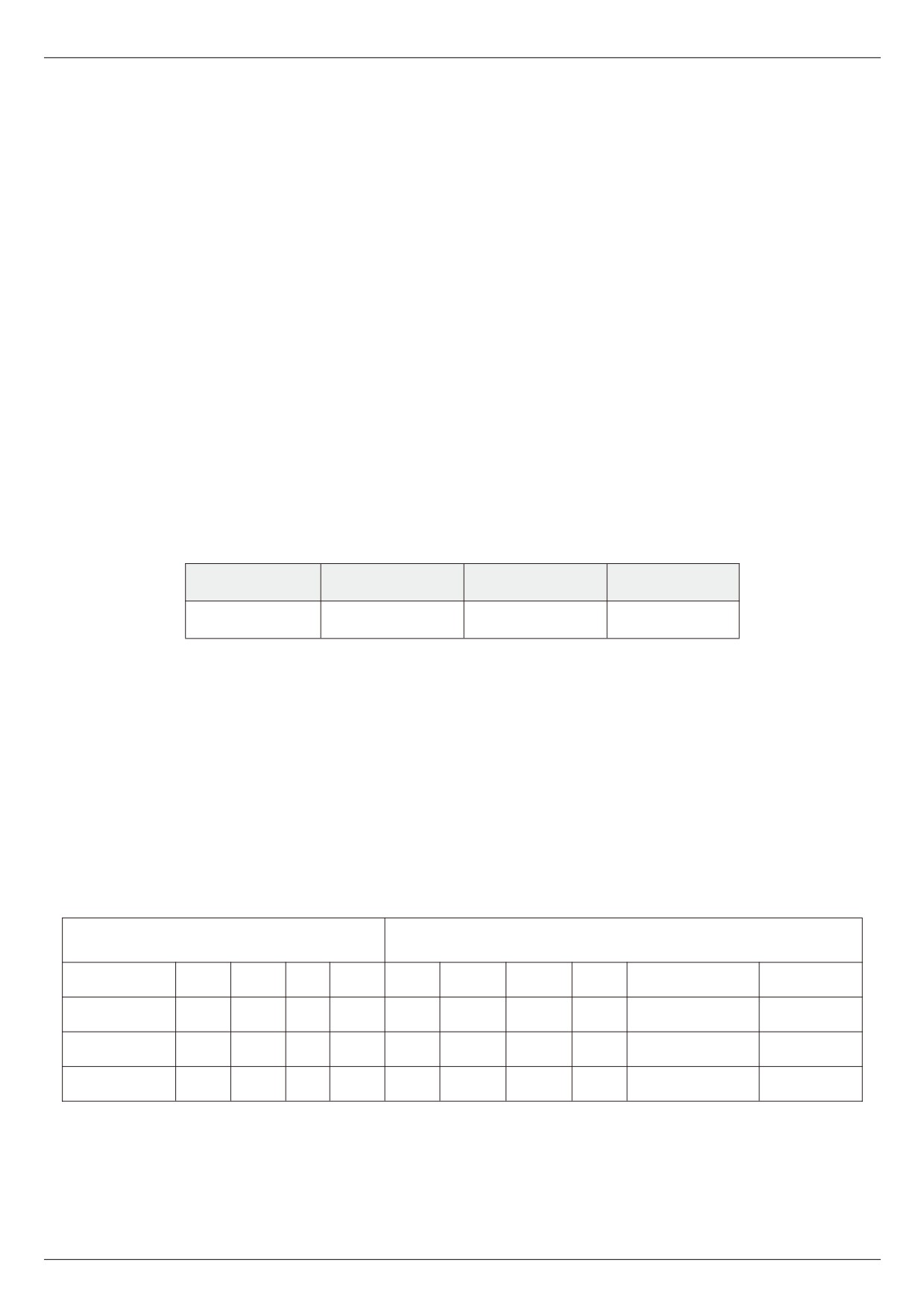
Characters or bytes are transmitted from left to right, as shown in the following table:
< - least significant bit ( LSB )
Most significant bit ( msb ) - >
Starting bit
1
2
3
4
5
6
7
8
Stop bit
-
Starting bit
1
2
3
4
5
6
7
8
Even check
Stop bit
Starting bit
1
2
3
4
5
6
7
8
Odd check
Stop bit
Starting bit
1
2
3
4
5
6
7
8
Stop bit
Stop bit
The above table shows that RTU transmission mode
Information frames are separated by at least at static interval of 3.5 bytes. The entire frame must be transmitted
in a continuous stream of bytes. If the interval between more than two frames is less than 3.5 bytes, the receiving
device will mistakenly assume that the slave station address of the second frame is the continuation of the previous
- 150 -
Appendix A Introduction of Communication
frame. CRC check failed due to frame disorder, resulting in communication failure. If the rest interval between two
bytes exceeds 1.5 bytes, the receiving device will consider the information frame incomplete and discard it.
2.2 MODBUS communication interface
Modbus realizes communication through RS485 interface, that is, through 485 + / 485 - link on the control panel.
2.3 MODBUS function and information format
Modbus's main function is to read (read) and modify (write) parameters. Different function instructions determine
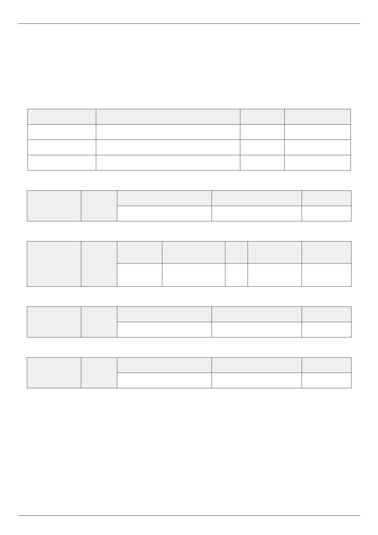
different operation requests. The MODBUS function of HV480 is shown in the following table:
Functional instruction
Function name
Broadcasting
Maximum value of N
0x03
Reading N register words
No
16
0x06
Modify a register ( power down save )
Yes
1
0x05
Modify a register ( power down does not save )
Yes
1
Different function commands determine different Modbus information formats, as follows:
Starting word address
Word number
CRC16
Slave number
0x03
High | low
High | low
Low | high
Function instruction 3 _ host request
Bytes
Starting word value
-
Last word value
CRC16
Slave number
0x03
High | low
High | low
-
High | low
Low | high
Function command 3 _ host response
Starting word address
Data
CRC16
Slave number
0x06
High | low
High | low
Low | high
Function instruction 6 _ host request and slave response (same format)
Starting word address
Data
CRC16
Slave number
0x05
High | low
High | low
Low | high
Function instruction 5 _ host request and slave response (same format)
Function example
Function 0x03: read n register words, read range 1 ~ 16
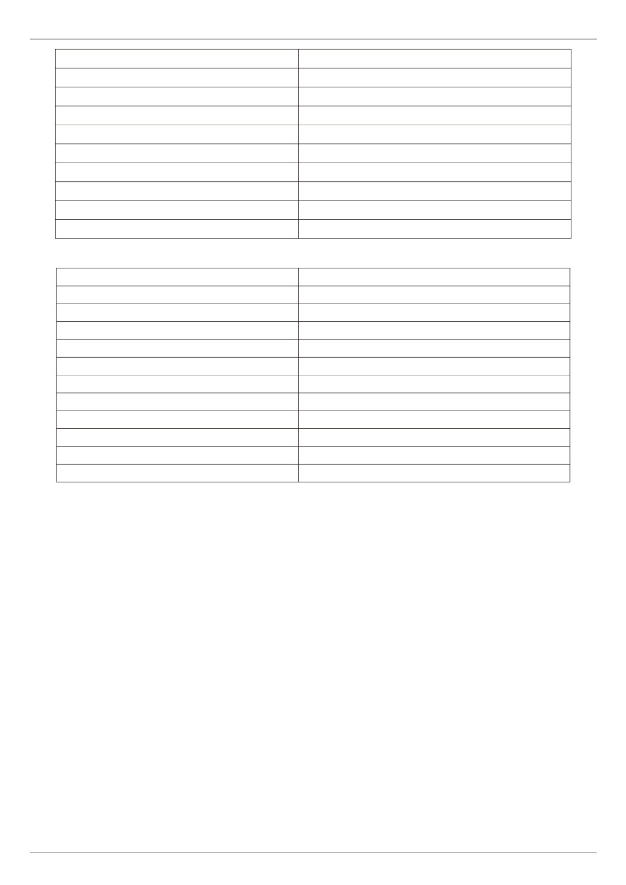
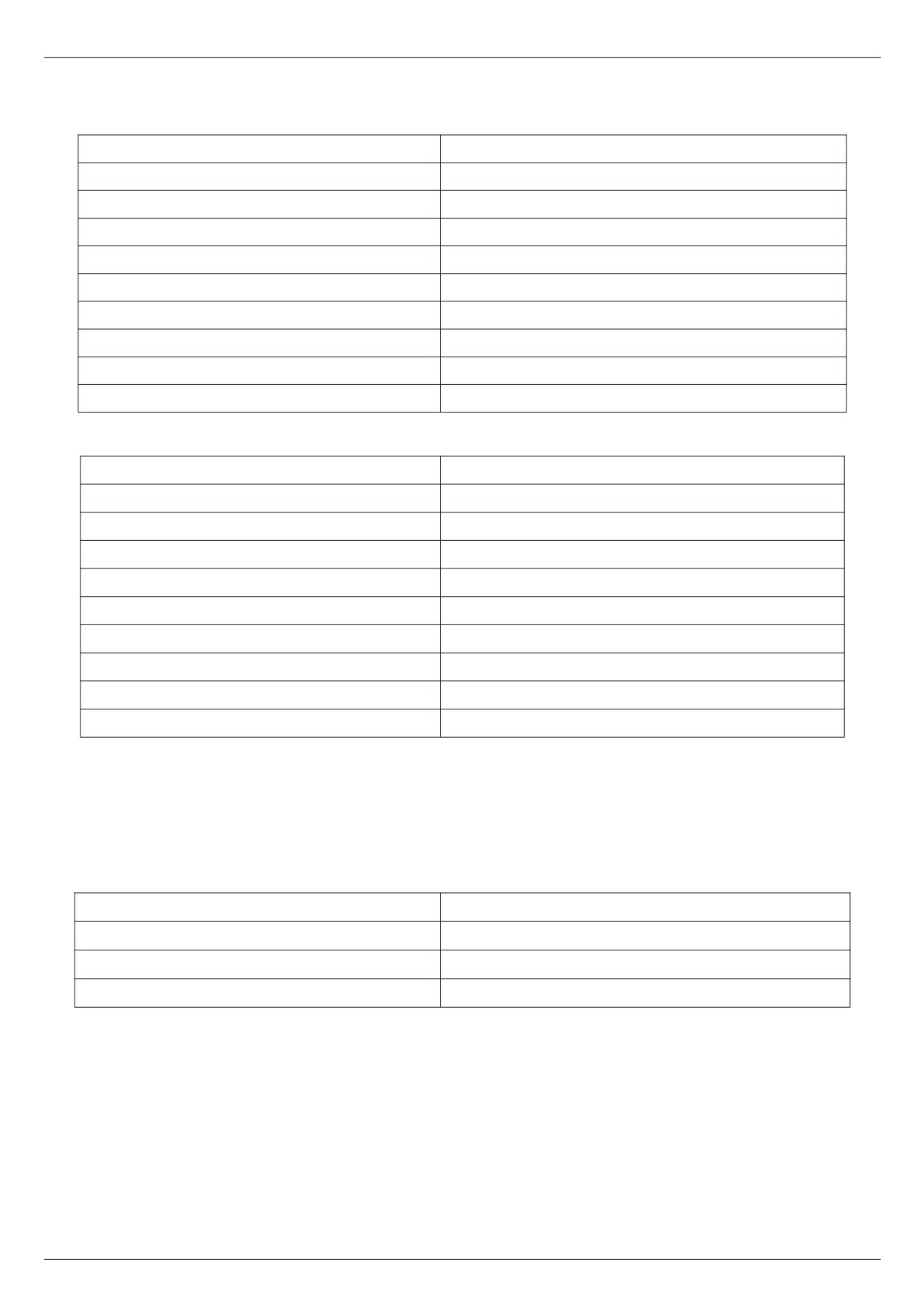
The slave address is 01h, and two consecutive data words are read first. The starting address is F000H of the
communication parameter register. The structure of the frame is described as follows:
- 151 -
Appendix A Introduction of Communication
Message start
3.5 bytes of transmission time
Slave address
0 1H
Modbus function code
0 3H
Starting address high byte
F 0H
Starting address low byte
0 0H
High byte of data
0 0H
Low byte of data
0 2H
CRC low byte
F 7H
CRC high byte
0 BH
End of message
3.5 bytes of transmission time
Function instruction 0x03 requests frame
Message start
3.5 bytes of transmission time
Slave address
0 1H
Modbus function code
0 3H
High number of data bytes
0 0H
Low number of data bytes
0 4H
Register F000H data high byte
0 0H
Register F000H data high byte
0 BH
Register F000H data high byte
0 0H
Register F000H data high byte
0 0H
CRC low byte
CRC high byte
End of message
3.5 bytes of transmission time
Function instruction 0x03 slave responds to frame
Function
0x06: modify a register word.
Note: frequent write operations can damage internal memory!
① Execute the write command, and the data will be written into the internal register. The memory has a limit on
the number of write operations. If the limit is exceeded, the memory address will be destroyed. Please avoid frequent
write operations.
② If it is necessary to write to an address frequently, it is recommended to use function instruction 0x05.
- 152 -
Appendix A Introduction of Communication
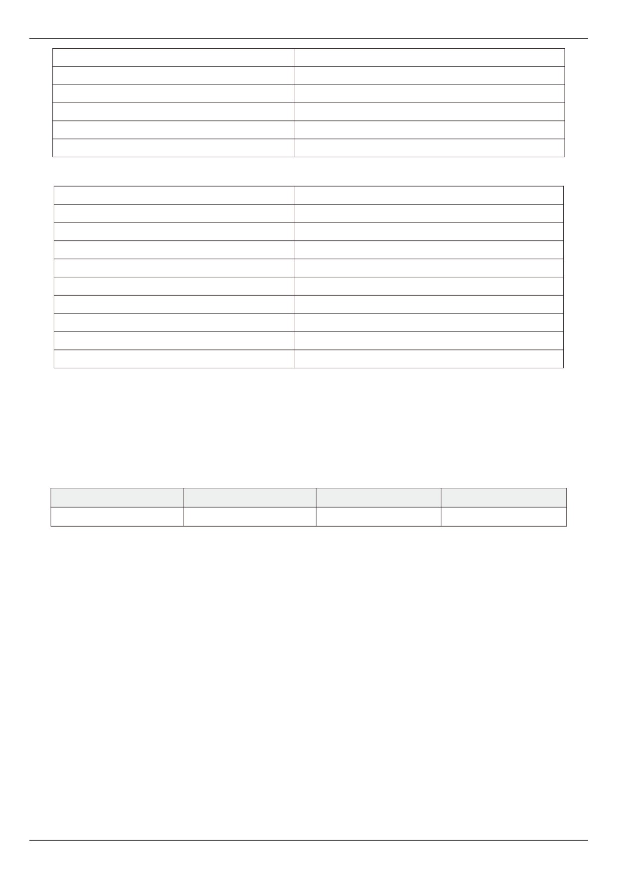
Example: slave address is 01h. Now modify the contents of a register. Its communication register address is
f08h, and the written content is 1388 H. The structure of the frame is described as follows:
Message start
3.5 bytes of transmission time
Slave address
01H
Modbus function code
06H
Starting address high byte
F0H
Starting address low byte
08H
High byte of data
00H
Low byte of data
01H
CRC low byte
FAH
CRC high byte
C8H
End of message
3.5 bytes of transmission time
Function
0x06 host requests
Message start
3.5 bytes of transmission time
Slave address
01H
Modbus function code
06H
Starting address high byte
F0H
Starting address low byte
08H
High byte of data
00H
Low byte of data
01H
CRC low byte
CFH
CRC high byte
C8H
End of message
3.5 bytes of transmission time
Function
0x06 slave responds.
Function
0x05: modify a register word and write it into ram.
Note: the write operation instruction only modifies ram, does not store internal memory, and does not
save when power fails!
Example: slave address is 01h, now modify the contents of a register whose communication register address is
f08h, written in the content is 01h. The structure of the frame is described as follows:
Message start
3.5 bytes of transmission time
Slave address
01H
Modbus function code
05H
Starting address high byte
F0H
- 153 -
Appendix A Introduction of Communication
Starting address low byte
08H
High byte of data
00H
Low byte of data
01H
CRC low byte
BEH
CRC high byte
C8H
End of message
3.5 bytes of transmission time
Function
0x05 host requests
Message start
3.5 bytes of transmission time
Slave address
01H
Modbus function code
05H
Starting address high byte
F0H
Starting address low byte
08H
High byte of data
00H
Low byte of data
01H
CRC low byte
BEH
CRC high byte
C8H
End of message
3.5 bytes of transmission time
Function
0x05 slave responds.
Fault code and exception code
If the slave successfully receives a request but cannot execute it, the slave will return an exception response
containing the fault code and the exception generation code, informing the host of the error message.
The fault code format is in two formats:
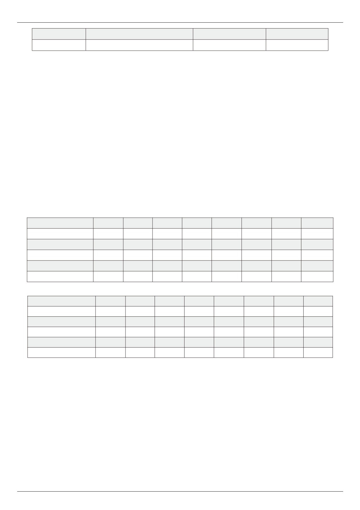
When FD - 06 = 0, the exception code is shown in the following table:
Slave code
Fault code
Exception code
CRC16
8000H
Low | high
The HV480 exception code is as follows:
① 1 = parameter cannot be modified because password protection is turned on.
② 2 = slave cannot recognize the requested function instruction. That is(not 3, 5, 6)
③ 3 = CRC check error.
④ 4 = slave does not contain the requested word address.
⑤ 5 = this parameter is invalid and out of range.
⑥ 6 = parameter is read-only and cannot be modified.
⑦ 7 = the system locks this parameter.
When FD - 06 = 1, the exception code is shown in the following table:
- 154 -
Appendix A Introduction of Communication
Slave code
Fault code
Exception code
CRC16
Function instruction + 0x80
Low | high
① 1 = Parameter cannot be modified because password protection is turned on.
② 2 = Slave cannot recognize the requested function instruction. That is(not 3, 5, 6).
③ 3 = CRC check error.
④ 4 = Slave does not contain the requested word address.
⑤ 5 = This parameter is invalid and out of range.
⑥ 6 = Parameter is read-only and cannot be modified.
⑦ 7 = The system locks this parameter.
2.4 Communication mapping register address distribution
Frequency inverter parameter register set and function code one-to-one correspondence. Read and write
frequency inverter parameter registers via Modbus communication the contents in the can realize the read-write
operation of the corresponding function code. The read-write characteristics and scope of the function codes follow
the definition of the function parameters of the frequency inverter. The address of the frequency inverter parameter
register consists of a high byte and a low byte. The high byte code function code group number and the low byte
represent the function code serial number in the corresponding function code group. The corresponding relationship
is shown in the following table:
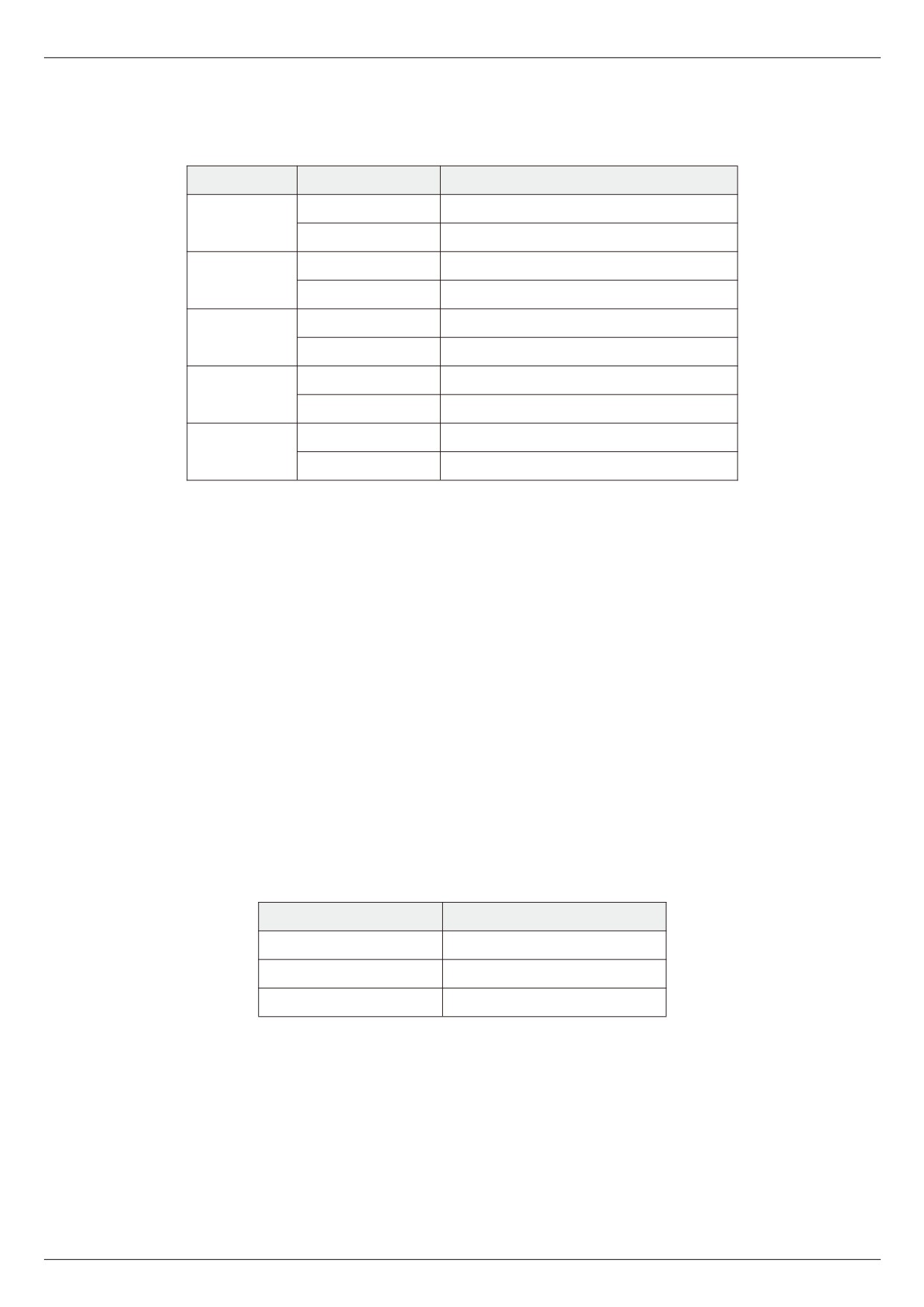
Read operation and write EEPROM operation (write saved by power failure) address mapping table:
Address high byte
0xF0
0x F1
0x F2
0x F3
0x F4
0x F5
0x F6
0x F7
Parameter group
F0 group
F1 group
F2 group
F3 group
F4 group
F5 group
F6 group
F7 group
Address high byte
0x F8
0x F9
0x FA
0x FB
0x FC
0x FD
0x FE
0x FF
Parameter group
F8 group
F9 group
FA group
FB group
FC group
FD group
FE group
FF group
Address high byte
0x 1F
0x A0
0x A1
0x A2
0 x 70
0x AF
Parameter group
FH group
Po group
P1 group
P2 group
U0 group
E0 group
Write only ram operation (write without saving when power fails) address mapping table:
Address high byte
0x00
0 x 01
0 x 02
0 x 03
0 x 04
0 x 05
0 x 06
0 x 07
Parameter group
F0 group
F1 group
F2 group
F3 group
F4 group
F5 group
F6 group
F7 group
Address high byte
0 x 08
0 x 09
0x 0A
0x 0B
0x 0C
0x 0D
0x 0E
0x 0F
Parameter group
F8 group
F9 group
FA group
FB group
FC group
FD group
FE group
FF group
Address high byte
0x 2F
0 x 40
0 x 41
0 x 42
Parameter group
FH group
Po group
P1 group
P2 group
Note: frequent write operations can damage internal memory!
① Execute the write command, and the data will be written into the internal register. The memory has a limit on
the number of write operations. If the limit is exceeded, the memory address will be destroyed. Please avoid frequent
write operations.
② If it is necessary to write to an address frequently, it is recommended to use the function instruction 0x05 or
the address of the write ram operation.
Communication control frequency / torque special register address 1000 h (readable / writable)
When frequency source F0 - 03 = 9, the setting frequency of the frequency inverter can be modified by writing
data to this address. Scope of data - 10,000 - 10,000, corresponding to a given value of - 100.00 % - 100.00 %.
The communication reads the 1000 h register value, and the response data word is the communication setting
value.
- 155 -

Appendix A Introduction of Communication
Common monitoring address (read - only)
Communication address
Address description
1001H
Operating frequency ( unit: 0.01 Hz )
1002H
Bus voltage ( unit: 1v )
1003H
Output voltage ( unit: 1v )
1004H
Output current ( unit: 1v )
1005H
Output frequency ( unit: 0.1 kw )
1006H
Output torque ( unit: 0.1 % )
1007H
running speed
1008H
X input terminal status
1009H
Output terminal status
100AH
AI1 voltage ( unit: 0.01 v )
100BH
AI2 voltage ( unit: 0.01 v )
100CH
AI3 voltage ( unit: 0.01 v )
100EH
loading speed
1013H
Feedback frequency ( unit: 0.1 Hz )
101EH
Encoder feedback frequency ( unit: 0.01 Hz )
- 156 -
Appendix A Introduction of Communication
Communication control output terminal special register address 2001 H (write only)
When the terminal output function is set to 20, the state of the output terminal can be controlled by writing a
response value to the register through communication. The specific definitions of each are shown in the following
table:
Position
value
Description
0
DO1 output is invalid
0
1
DO1 output is valid
0
Reserve
1
1
Reserve
0
Relay 1 output is invalid
2
1
Relay 1 output is valid
0
Reserve
3
1
Reserve
0
FM output is invalid
4
1
FM output valid
Communication control AO1 output special register 2002H (write only)
When the analog output AO1 output function is selected to be 12: communication setting, the communication
address can be used to realize the right the analog ao1 control of the frequency inverter defines a quantization
relation of 0 ~ 7 FFF representing 0 % ~ 100 %.
Communication control AO2 output special register 2003H (write only)
When the analog output AO2 output function is selected to be 12: communication setting, the communication
address can be used to realize the right the analog ao2 control of the frequency inverter defines a quantization
relation of 0 ~ 7 FFF representing 0 % ~ 100 %.
Communication control FMP output special register 2004 H (write only)
When the pulse output FMP output function is selected to be
12: communication setting, through this
communication address, it is possible to realize the right the frequency inverter pulse quantity FMP is controlled, and
the defined quantization relation is 0 ~ 7 FFF, which represents 0 % ~ 100 %.
Communication status feedback special register address 3000 H (read - only).
Reading this register can monitor the current running status of the frequency inverter. This register is read - only.
Each value. Define the following table:
value
Description
1
Forward running
2
Reverse operation
3
Stop
Communication read fault code special register address 8000 h (read - only).
By reading this register, the current fault code of the frequency inverter can be monitored. When there is no fault, the
read data word is 0.
Communication control special register address 2000 h (write only)
- 157 -

Appendix A Introduction of Communication
value
Description
1
Forward running
2
Reverse operation
3
Forward jog
4
Reverse JOG
5
Free stop
6
Deceleration shutdown
7
Fault reset
The control mode is F0 - 02 = 2. By writing the corresponding data word into the communication control command
word 2000 H, the operation / stop / jog / reset of the frequency inverter can be controlled.
2.5 CRC 16 check method:
CRC (cyclic redundancy check) uses RTU frame format, and the message includes error detection domain
based on CRC method. The CRC field detects the content of the entire message. The CRC field is two bytes and
contains 16 - bit binary values. It is calculated by the transmission device and added to the message. The receiving
device recalculates the CRC of the received message and compares it with the value in the received CRC field. If the
two CRC values are not equal, then there is an error in the transmission.
CRC is stored in 0xffff first, and then calls a procedure to process the consecutive 8 - bit bytes in the message with
the value in the current register. Only 8bit data in each character is valid for CRC, and neither start bit nor stop bit nor
parity bit is valid.
During CRC generation, each 8 - bit character is exclusive or (xor) different from the register contents. The result
is shifted toward the least significant bit and the most significant bit is filled with 0. LSB is extracted and detected. If
LSB is 1, the register is different from the preset value or if LSB is 0, it will not be carried out. The whole process has
to be repeated eight times. After the last bit (bit 8) is completed, the next 8 - bit byte differs from the current value of
the register or separately. The value in the final register is the CRC value after all bytes in the message are executed.
When CRC is added to the message, the low byte is added first and then the high byte. The CRC simple
function is as follows:
unsigned int crc_chk_value(unsigned char *data_value,unsigned char length){
unsigned int crc_value=0xFFFF;
int i;
while(length--)
{
crc_value^=*data_value++;
for(i=0;i<8;i++)
{
if(crc_value&0x0001)
{
crc_value=(crc_value>>1)^0xa001;
}
else
{
crc_value=crc_value>>1;
}
}
}
return(crc_value);
}
- 158 -
Appendix A Introduction of Communication
2.6 Set up of communication network
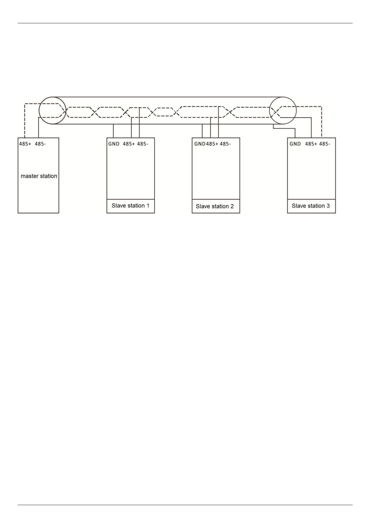
Communication network as shown in the figure below, the main station is PC, PLC or other communication
equipment, and the frequency inverters are slave station, sampling shielded twisted cable shall be connected. The
slave station of the network terminal needs external terminal resistance, which is recommended to be 120 ohms and
0.25 W.
Network topology map.
Notes:
Only when the frequency inverter is powered OFF can it be connected.
Networking suggestion
① connect RS485 link with cable shielded by double glue.
② Modbus cable should be far away from power drive line (at least 30cm).
③ avoid crossing Modbus cable and power line. If it cannot be avoided, please cross vertically.
④ connect the cable shielding layer to the protective ground, or connect the cable shielding layer to the
equipment ground if the equipment ground is already connected to the protective ground. Do not connect RS485
network directly to ground at any point.
⑤ Under any circumstances, avoid grounding wires forming a loop.
- 159 -
Appendix B Technical specification for HV480 series frequency inverters
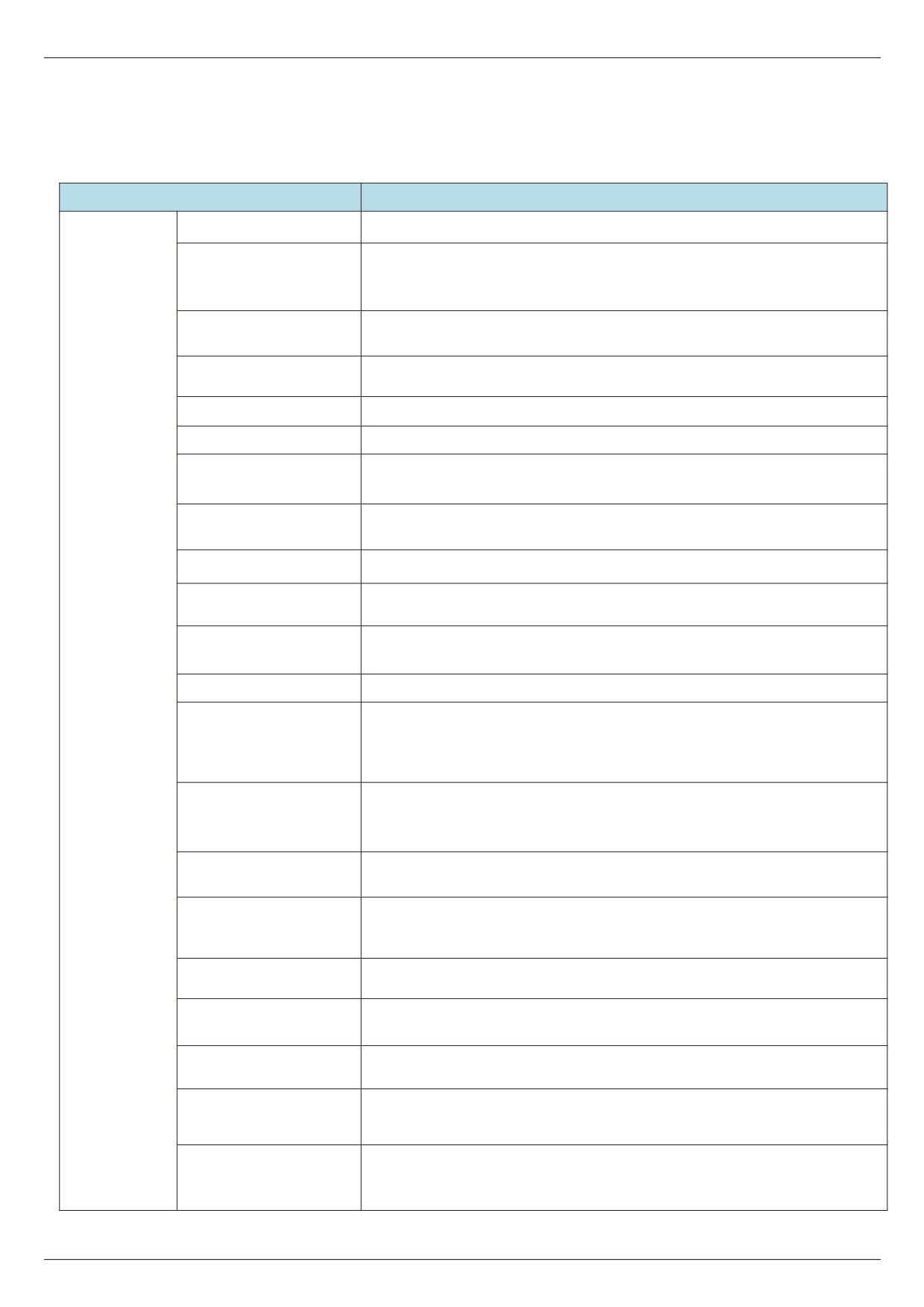
Appendix B Technical specification for HV480 series frequency inverters
Item
Specifications
Highest frequency
Vector control: 0 ~ 300 Hz V/F control: 0:3200Hz
0.5kHz~16kHz
Carrier frequency
The carrier frequency can be automatically adjusted according to the
load characteristics.
Input frequency
Digital setting: 0.01 Hz analog setting: highest frequency * 0.025 %
resolution
Open loop vector control
Control mode
V/F control
Pull-in torque
Model G machine: 0.5 Hz / 150 %
Speed control range
1:100
Speed stabilization
±0.5%
accuracy
Torque control
±5%
accuracy
Overload capacity
G: 150 % rated current 60s; 180 % rated current 3s.
Automatic torque increase; The manual torque is increased by 0.1
%-
Torque increase
30.0 %
Three ways: linear; Multipoint type; N - power V/F curve
V/F curve
( power 1.2, power 1.4, power 1.6, power 1.8, power 2 )
V/F separation
Two methods: full separation and half separation
Basic
Functionalities
Straight line or S curve acceleration and deceleration mode.
Acceleration and
Four kinds of acceleration and deceleration times,
deceleration curve
The acceleration and deceleration time range is 0.0 to 6500.0 S.
DC braking frequency: 0.00 Hz ~ maximum frequency
DC brake
Braking time: 0.0s ~ 36.0s
Brake action current value: 0.0 % - 100.0 %
JOG frequency range: 0.00 Hz ~ 50.00 Hz. JOG acceleration and
JOG
deceleration time 0.0s ~ 6500.0 s.
Simple PLC,
multi-stage speed
Up to 16 - speed operation via built-in PLC or control terminal
operation
Closed-loop control system capable of conveniently realize process
Built - in PID
control
Automatic voltage
When the grid voltage changes, the output voltage can be automatically
regulation ( AVR )
kept constant.
Over - voltage and
Automatically limit the current and voltage during operation to prevent
over-loss rate control
frequent over current and Over voltage trips.
Fast current limiting
Minimize over-current faults and protect the normal operation of the
function
frequency inverter
The " excavator" feature automatically limits the torque during operation
Torque limitation and
to prevent frequent over current trips; Open loop vector mode can
control
realize torque control
- 160 -
Appendix B Technical specification for HV480 series frequency inverters
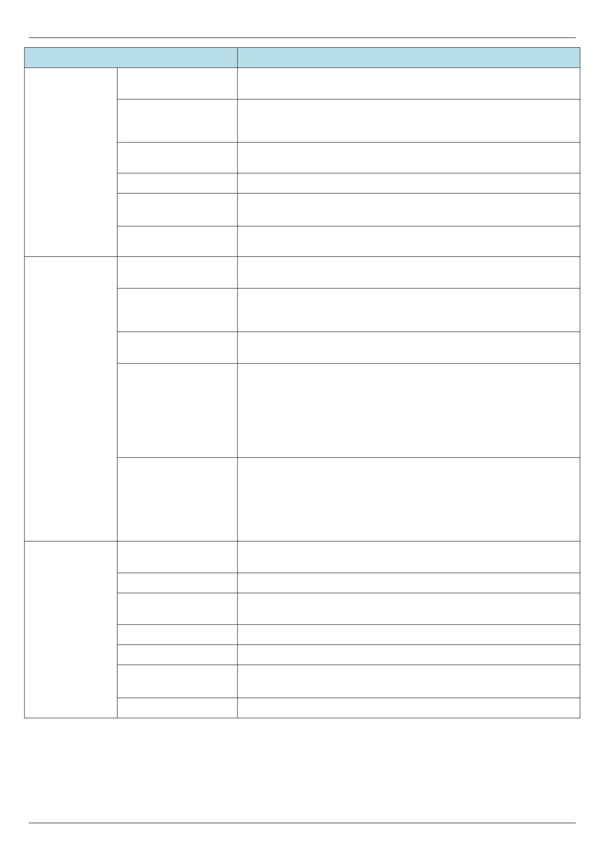
Item
Specifications
Outstanding
Using high performance current vector control technology to realize
performance
asynchronous motor control
When the instantaneous power failure occurs, the load feedback
Stop at once
energy compensates for the voltage drop and the frequency inverter
will continue to operate for a short period of time.
Individualized
Fast current limiting
Avoiding frequent over current faults of the frequency inverter
performance
Timing control
Timing control function: set the time range from 0.0 min to 6500.0 min
Switch between two
Two sets of motor parameters can realize switching control of two
motors
motors
Multithreaded bus
Supports a variety of fieldbus: RS - 485, CANopen
support
Operation panel setting, control terminal setting, serial communication
Command source
port setting. Can be switched in various ways
Multiple frequency sources: digital setting, analog voltage setting,
frequency source
analog current setting, pulse setting, serial port setting. Can be
switched in various ways
Auxiliary frequency
Various auxiliary frequency sources. Can flexibly realize auxiliary
source
frequency fine tuning and frequency synthesis
Standard 8 digital input terminals, of which 1 supports high-speed
Running
pulse input of up to 100 khz; Three analog input terminals, one
Input terminal
supporting only 0 ~ 10v voltage input, one supporting 0 ~ 10v voltage
input or 4 ~20mA current input,
1 analog input terminal, supporting DC±10V or ±(4~20mA)
1 high-speed pulse output terminal ( optional open collector type ),
supporting square wave signal output of 0 ~ 100 khz
1 digital output terminal
Output terminals
1 relay output terminal
2 analog output terminals to support 0 ~ 20ma current output or 0 ~
10v voltage output
Dust - free, metal dust, corrosive gases, flammable gases, oil fog, salt
Place of use
fog, water vapor, dripping direct sunlight - free indoor
Altitude
Below 1,000 meters
Ambient temperature
-10℃~40℃
Environment
Humidity
Less than 90 % RH without condensation
Vibration
Less than 0.5g.
Storage temperature
-25℃~65℃
Protection grade
IP20
- 161 -
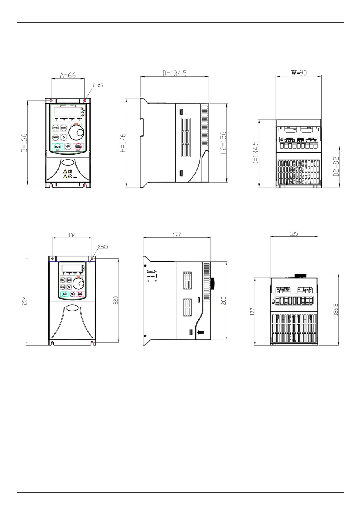
Appendix C External dimensions and installation dimensions
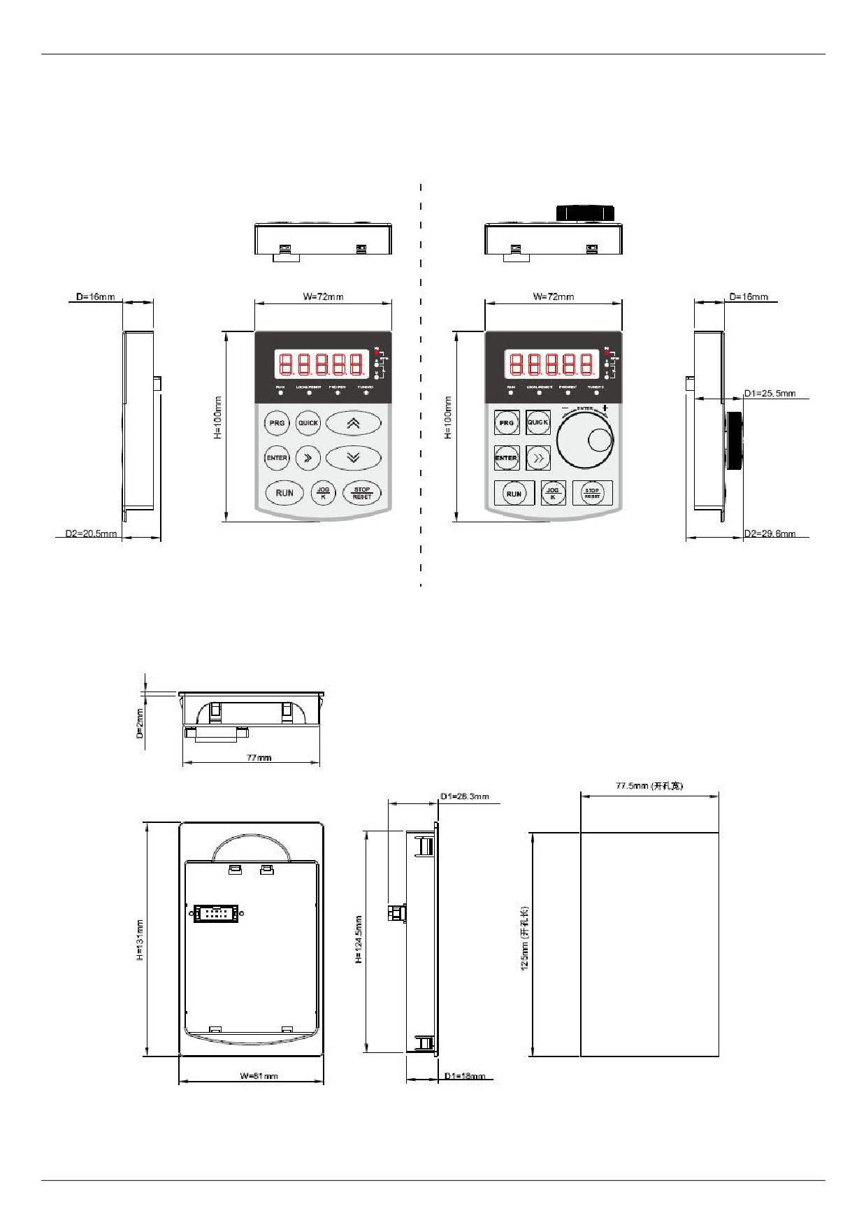
Appendix 1 general purpose keyboard dimensions and mounting dimensions
Fig a (keyboard operation in two ways)
Fig. b (keyboard bracket and hole size drawing)
- 162 -
Appendix C External dimensions and installation dimensions
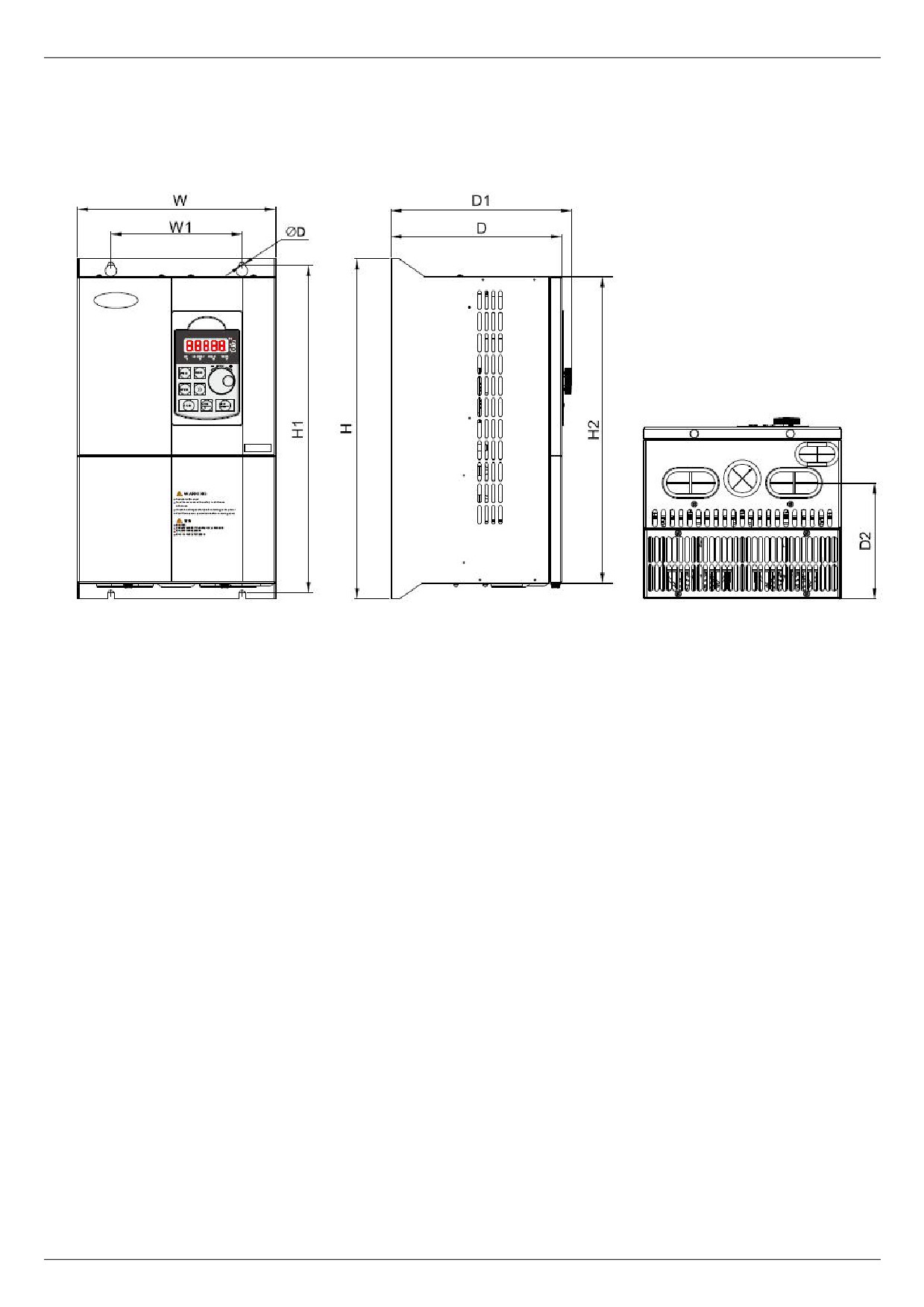
Appendix II Plastic shell dimensions and mounting dimensions
Fig 1(R75G3-2R2G3)
Fig 2(004G3-7R5G3)
- 163 -
Appendix C External dimensions and installation dimensions
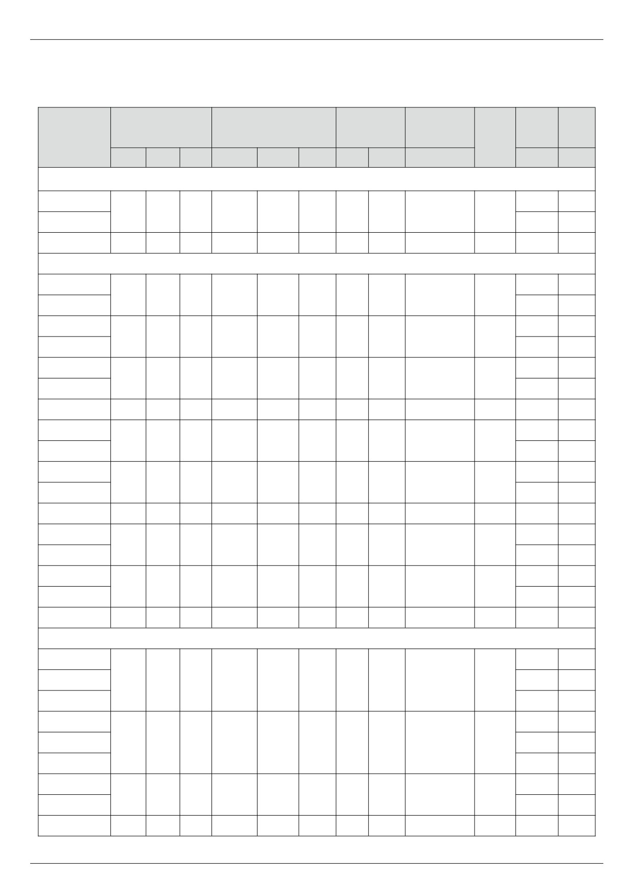
Appendix III dimensions and mounting dimensions of sheet metal machines
Fig 3(011G3-200G3)
- 164 -
Appendix C External dimensions and installation dimensions
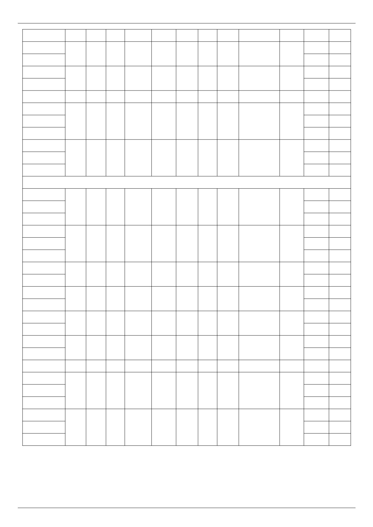
List of dimensions and mounting dimensions
Mounting
External dimension
Installation hole location
N.W
G.W
aperture
( mm )
( mm )
(kg)
(kg)
Model
Figure
( mm )
W
H
D
W1
H1
D1
H2
D2
d
G1 input voltage range: Single-phase AC220V±15%, 50 / 60 Hz
HV480-R75G1
1
1.3
80
130
128
70
120
140
4.5
1
HV480-1R5G1
1
1.3
HV480-2R2G1
125
220
166
110
205
177
124
6.5
1
2.3
2.8
G2 input voltage range: Three-phase AC220V±15%,
50
/
60 Hz
HV480-R75G2
1
1.3
90
176
134
66
166
145
156
82
5
1
HV480-1R5G2
1
1.3
HV480-2R2G2
2.3
2.8
125
234
177
104
220
188
205
/
5
2
HV480-004G2
2.3
2.8
HV480-5R5G2
6.4
7
170
301
188
110
285
193
264
128
5
3
HV480-7R5G2
6.4
7
HV480-011G2
195
330
185
150
315
197
284
130
6
3
7.6
8.7
HV480-015G2
11
12
227
388
196
150
375
206
350
133
7
3
HV480-018G2
11
12
HV480-022G2
18.5
20
275
498
210
180
477
220
459
157
7
3
HV480-030G2
18.5
20
HV480-037G2
307
557
266
230
537
278
501
204
9
3
30
41
HV480-045G2
37
50
377
628
280
240
600
292
568
228
9
3
HV480-055G2
37
50
HV480-075G2
60
82
500
788
350
270
762
357
728
226
13
3
HV480-093G2
60
82
HV480-110G2
540
900
348
320
867
358
828
278
13
3
84
110
G3
input voltage range: Three-phase AC
380~440 (-15%~+10%), 50 /
60
Hz
HV480-R75G3
1
1.3
HV480-1R5G3
90
176
134
66
166
145
156
82
5
1
1
1.3
HV480-2R2G3
1
1.3
HV480-004G3
2.3
2.8
HV480-5R5G3
125
234
177
104
220
188
205
/
5
2
2.3
2.8
HV480-7R5G3
2.3
2.8
HV480-011G3
6.4
7
170
301
188
110
285
193
264
128
5
3
HV480-015G3
6.4
7
HV480-018G3
195
330
185
150
315
197
284
130
6
3
7.6
8.7
- 165 -
Appendix C External dimensions and installation dimensions
HV480-022G3
7.6
8.7
HV480-030G3
11
12
227
388
196
150
375
206
350
133
7
3
HV480-037G3
11
12
HV480-045G3
18.5
20
275
498
210
180
477
220
459
157
7
3
HV480-055G3
18.5
20
HV480-075G3
307
557
266
230
537
278
501
204
9
3
30
41
HV480-093G3
37
50
HV480-110G3
377
628
280
240
600
292
568
228
9
3
37
50
HV480-132G3
37
50
HV480-160G3
60
82
HV480-185G3
500
788
350
270
762
357
728
226
13
3
60
82
HV480-200G3
60
82
G4 input voltage range: Three-phase AC
460~480
(-15%~+10%),
50
/
60 Hz
HV480-R75G4
1
1.3
HV480-1R5G4
90
176
134
66
166
145
156
82
5
1
1
1.3
HV480-2R2G4
1
1.3
HV480-004G4
2.3
2.8
HV480-5R5G4
125
234
177
104
220
188
205
/
5
2
2.3
2.8
HV480-7R5G4
2.3
2.8
HV480-011G4
6.4
7
170
301
188
110
285
193
264
128
5
3
HV480-015G4
6.4
7
HV480-018G4
7.6
8.7
195
330
185
150
315
197
284
130
6
3
HV480-022G4
7.6
8.7
HV480-030G4
11
12
227
388
196
150
375
206
350
133
7
3
HV480-037G4
11
12
HV480-045G4
18.5
20
275
498
210
180
477
220
459
157
7
3
HV480-055G4
18.5
20
HV480-075G4
307
557
266
230
537
278
501
204
9
3
30
41
HV480-093G4
37
50
HV480-110G4
377
628
280
240
600
292
568
228
9
3
37
50
HV480-132G4
37
50
HV480-160G4
60
82
HV480-185G4
500
788
350
270
762
357
728
226
13
3
60
82
HV480-200G4
60
82
- 166 -
Appendix D HV480 series inverter specifications
Appendix D HV480 series inverter specifications
Input current
Output current
Adaptive motor
Power supply capacity
Frequency inverter model
(A)
(A)
(KW)
(HP)
(KVA)
G1
input voltage range: Single-phase AC220V±15%, 50 / 60
Hz
HV480-R75G1
11.0
4.0
0.75
1
3.0
HV480-1R5G1
18.0
7.0
1.5
2
4.8
HV480-2R2G1
27.0
9.6
2.2
3
7.1
G2
input voltage range: Three-phase AC220V±15%, 50 /
60
Hz
HV480-R75G2
5
3.8
0.75
1
3
HV480-1R5G2
5.8
5.1
1.5
2
4.0
HV480-2R2G2
10.5
9.0
2.2
3
5.9
HV480-004G2
14.6
13.0
3.7
5
8.9
HV480-5R5G2
26.0
25.0
5.5
7.5
17
HV480-7R5G2
35.0
32.0
7.5
10
21
HV480-011G2
46.5
45
11
15
30
HV480-015G2
62
60
15
20
40
HV480-018G2
76
75
18
25
57
HV480-022G2
92
91
22
30
69
HV480-030G2
113
112
30
40
85
HV480-037G2
157
150
37
50
114
HV480-045G2
180
176
45
60
134
HV480-055G2
214
210
55
75
160
HV480-075G2
307
304
75
100
231
HV480-093G2
385
377
90
125
250
HV480-110G2
430
426
110
150
280
G3
input voltage range: Three-phase AC
380~440
(-15%~+10%),
50
/
60
Hz
HV480-R75G3
3.4
2.1
0.75
1
1.5
HV480-1R5G3
5.0
3.8
1.5
2
3.0
HV480-2R2G3
5.8
5.1
2.2
3
4.0
HV480-004G3
10.5
9.0
4.0
5
5.9
HV480-5R5G3
14.6
13.0
5.5
7.5
8.9
HV480-7R5G3
20.5
17.0
7.5
10
11
HV480-011G3
26.0
25.0
11
15
17
HV480-015G3
35.0
32.0
15
20
21
HV480-018G3
42
37
18.5
25
45
HV480-022G3
50
45
22
30
54
- 167 -
Appendix D HV480 series inverter specifications
HV480-030G3
68
60
30
40
65
HV480-037G3
83
75
37
50
63
HV480-045G3
102
91
45
60
81
HV480-055G3
124
112
55
75
97
HV480-075G3
169
150
75
100
127
HV480-093G3
203
176
90
125
150
HV480-110G3
248
210
110
150
179
HV480-132G3
256
253
132
175
192
HV480-160G3
307
304
160
220
231
HV480-185G3
350
340
185
245
242
HV480-200G3
385
377
200
270
250
G4
input voltage range: Three-phase AC 460~480 (-15%~+10%),
50
/ 60
Hz
HV480-R75G4
3.4
2.1
0.75
1
1.5
HV480-1R5G4
5.0
3.8
1.5
2
3.0
HV480-2R2G4
5.8
5.1
2.2
3
4.0
HV480-004G4
10.5
9.0
4.0
5
5.9
HV480-5R5G4
14.6
13.0
5.5
7.5
8.9
HV480-7R5G4
20.5
17.0
7.5
10
11
HV480-011G4
26.0
25.0
11
15
17
HV480-015G4
35.0
32.0
15
20
21
HV480-018G4
42
37
18.5
25
45
HV480-022G4
50
45
22
30
54
HV480-030G4
68
60
30
40
65
HV480-037G4
83
75
37
50
63
HV480-045G4
102
91
45
60
81
HV480-055G4
124
112
55
75
97
HV480-075G4
169
150
75
100
127
HV480-093G4
203
176
90
125
150
HV480-110G4
248
210
110
150
179
HV480-132G4
256
253
132
175
192
HV480-160G4
307
304
160
220
231
HV480-185G4
350
340
185
245
242
HV480-200G4
385
377
200
270
250
- 168 -
Attachment 1
Constant pressure control solution Case V0.1 for water pump and fan
1.1. Overview
The process PID closed-loop control regulates the rotation speed of the motor and indirectly controls the water
pressure or air pressure of the pipeline to be constant.
2.1 Two types of pressure sensors for pump and fan control
Type 1: 0 ~ 10v remote pressure gauge
Type 2: 4 ~ 20ma pressure transmitter
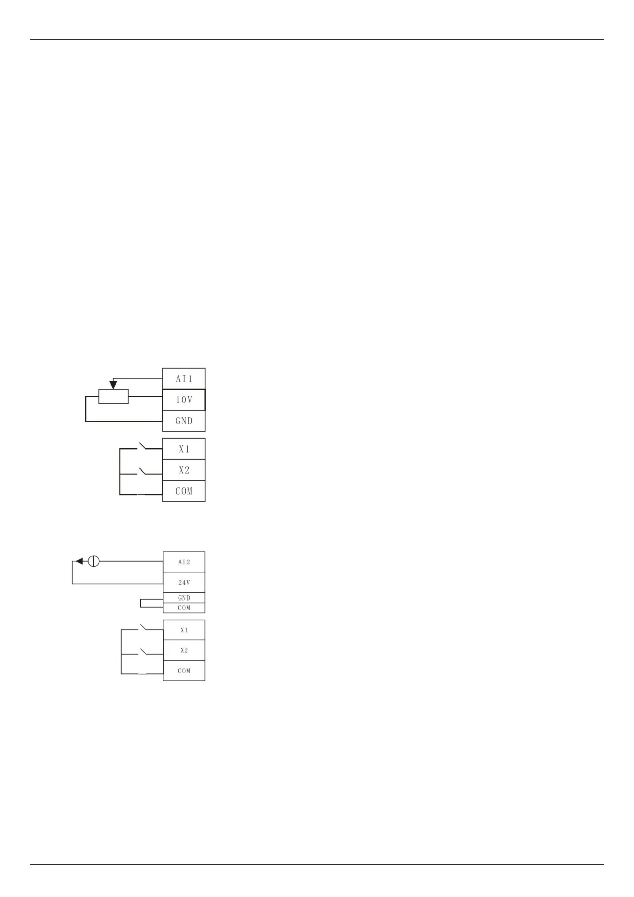
3.1 Control wiring diagram
Type 1: pressure sensor is 0 ~ 10v remote pressure gauge
Remote transmission pressure gauge signal 0 ~ 10v
Forward run
Reverse run
Type 2: the pressure sensor is a 4 ~ 20mA
Pressure transmitter
Pressure transmitter 4 ~ 20mA
Note: the control board AI2 jumper is shorted to the current input side
Forward run
Reverse run
- 169 -
Attachment 1
3.2 Setting parameters
Type 1: 0 ~ 10v remote transmission pressure gauge
Name
Function code
Numerical
Description
Control mode
F0-01
2
V/F control
Main frequency source
F0-03
8
PID constant pressure water supply
PID given source
FA-00
0
Pressure setting is set by FA - 01 parameter
PID value given
FA-01
25%
The set pressure is 2.5kg.
PID feedback source
FA-02
0
The pressure gauge is fed back to AI1 ( 0 ~ 10v input )
Name
Function code
Numerical
Description
PID feedback range
FA-04
1000
The measuring range of pressure gauge is 10kg
Proportional gain
FA-05
30
Integration time
FA-06
1
Selection of PID shutdown
FA-28
1
Continue calculation when shutdown
operation
Stress wake-up option
FA-29
1
Pressure wake-up is valid during sleep
Percentage of wake-up
It will be awakened when pipeline pressure is lower than 2.5 * 80
%
FA-30
80%
pressure
= 2kg
Wake - up delay time
FA-31
1s
Percentage of dormant
FA-32
100%
When the pipeline pressure is greater than the set pressure of 2.5kg,
pressure
it goes to sleep after 60s.
Pressure sleep delay time
FA-33
60s
Type 2: The 4 ~ 20ma pressure transmitter
Modifies the following parameters based on the type 1 parameters, and the control board AI2 jumper is shorted to the
current input side
Name
Function code
Numerical
Description
AI2 minimum input
F5-29
2.00
2v correspond to 4mA
PID feedback source
FA-02
1
The feedback source is AI2 ( 4 ~ 20ma current signal )
4.1 The sleep wake-up function
Has two sleep modes. During the control process, one of them can be selected according to actual needs.
1) Sleep according to pressure, that is, after the pressure reaches the sleep pressure threshold, the frequency
inverter stops outputting after a delay time.
Stress wake-up option
FA-29
1
Pressure wake-up is valid during sleep
Percentage of wake-up
It will be awakened when pipeline pressure is lower than 2.5 * 80 %
FA-30
80%
pressure
= 2kg
Wake - up delay time
FA-31
1s
Percentage of dormant
When the pipeline pressure is greater than the set pressure of 2.5kg,
FA-32
100%
pressure
it goes to sleep after 60s.
2) Sleep according to the frequency, that is, the frequency is lower than the sleep frequency threshold. After the
delay time, the frequency inverter stops outputting.
- 170 -

Attachment 1
Pressure wake-up is invalid during sleep ( according to wake-up
Stress wake-up option
FA-29
0
frequency )
When the set frequency is greater than 40hz, the frequency inverter wakes
Wakeup frequency
F8-14
40hz
up
Wake - up delay time
F8-15
1s
When the set frequency is lower than 25hz, enter the sleep state after 60
Sleep frequency
F8-16
25hz
seconds between F8 and 17 hours
3) No need to sleep
Stress wake-up option
FA-29
0
Pressure wake-up is invalid during sleep
Wakeup frequency
F8-14
0
Wake - up delay time
F8-15
0
Sleep frequency
F8-16
0
- 171 -
Attachment 2
Inquiry method of state parameters
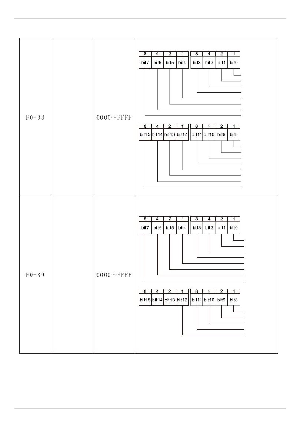
In the shutdown or running state, the > > shift key ON the operation panel switches the contents corresponding
to each byte of the function code F0 - 37 / 38 / 39 and can display multiple status parameters. There are 32 operating
state parameters in the operating state, and the function code F0 - 37 / 38 selects whether each corresponding
parameter is displayed according to the binary bit.
There are 13 shutdown state parameters under shutdown state, and the functional codes F0 - 39 select whether
each corresponding parameter is displayed according to the binary bit.
Correspondence between decimal system and hexadecimal system:
Decimal system
0123456789
10
11
12
13
14
15
Hexadecimal
0123456789
A
B
C
D
E
F
Examples:
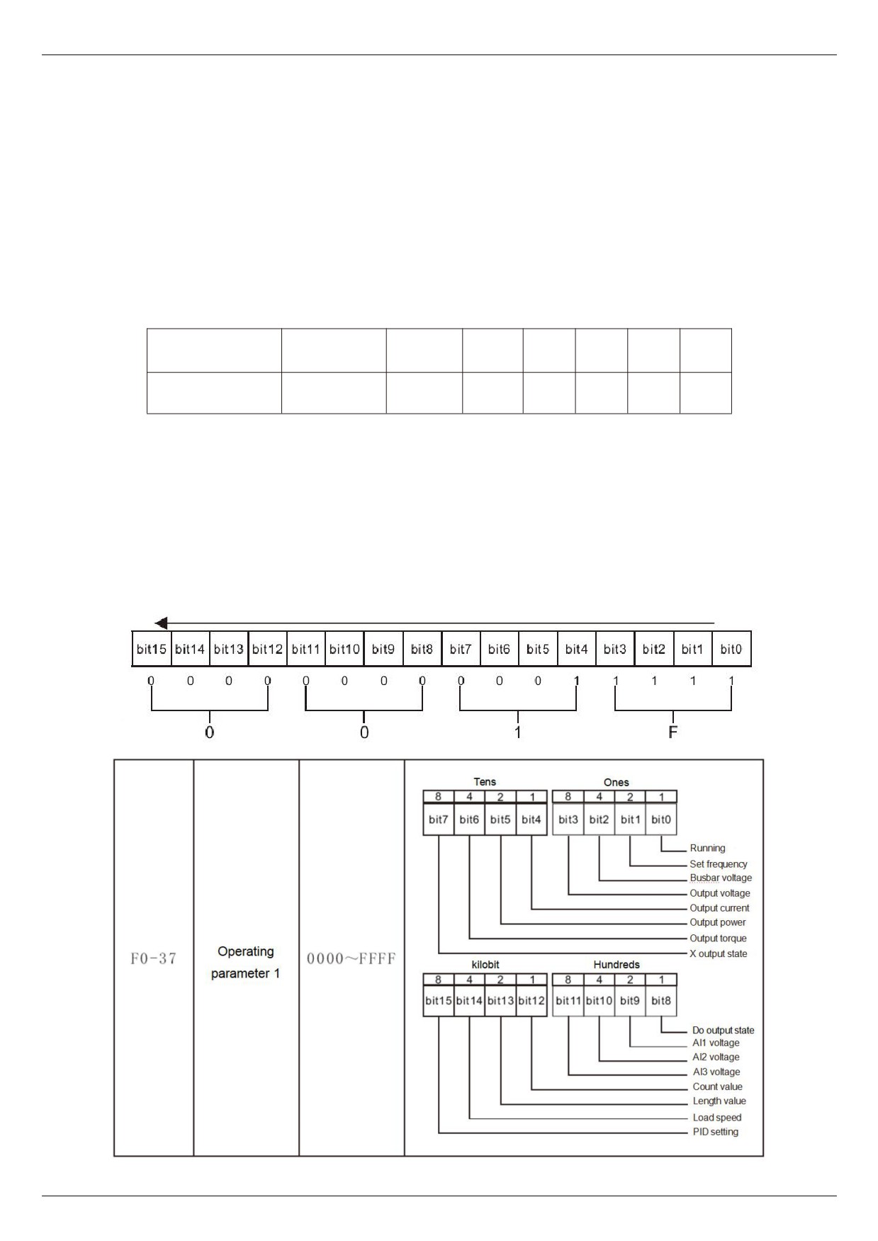
Check the parameters in the running state through the panel: (running frequency, bus voltage, output voltage,
output current,Output power, PID setting).
1. According to the correspondence between each byte in the function code F0 - 37 and the above parameters,
the corresponding bit is set to 1.
2. Set this binary number to F0 - 37 after converting it to hexadecimal. Keyboard setting value: h 001f.
3. Use the > > key on the operation panel to switch the corresponding contents of each byte of the function code
F0 - 37 in turn, and you can check the values of relevant parameters. Set as shown in the figure below:
High position
Low position
F0-37
Binary
hexadecimal
- 172 -
Attachment 2
Tens
Ones
PID feedback
PLC stage
PULSE input pulse frequency
Synchronous frequency
Remaining operating time
AI1 voltage before calibration
AI2 voltage before calibration
Operating
AI3 voltage before calibration
kilobit
Hundreds
parameter 2
Linear velocity
Current power-on time
Current run time
Input pulse frequency Hz
Communication settings value
Encoder feedback speed
Main frequency x
Secondary frequency y
Tens
Ones
Set frequency
Busbar voltage
X terminal input status
Do output state
AI1 voltage
AI2 voltage
Shutdown
AI3 voltage
parameter
Count value
kilobit
Hundreds
Length value
PLC stage
Loading speed
PID setting
X5 input frequency
- 173 -
Warranty agreement
The quality assurance of the product shall be handled according to the following regulations:
The warranty scope only refers to the drive body, and the warranty period starts from the Company's delivery
date.
The warranty period of the product is 18 months after purchase,If the failure is caused by the following reasons,
even within the warranty period, it will be paid maintenance:
z
Problems caused by incorrect operation or unauthorized self-repair and renovation;
z
Problems caused by using drivers beyond standard specification requirements;
z
Damage caused by falling or rough handling after purchase;
z
Aging or failure of devices caused by use in environments that do not meet the requirements of this
specification;
z
Drive damage caused by wrong connection line;
z
Failures caused by earthquakes, fires, geomantic disasters, lightning strikes, abnormal voltages or other
natural disasters and disasters.
The Company has the right to entrust others to take care of the warranty of the faulty products.
The quality assurance content that is truly the responsibility of the Company:
z
Return, exchange and warranty within one month of shipment;
z
Replacement and warranty within three months of shipment;
z
Warranty will be 18 months after shipment
Relevant service fees shall be calculated based on actual fees. If there is any agreement, the principle of
agreement first shall be applied.
The Company's sales, production and agency agencies throughout the country can provide after-sales service
to the product.
The power of interpretation of this agreement is vested in HNC
- 174 -