HV590 Series Frequency Inverter. User Manual (Version: 3.1.14) - page 6
Appendix I H5RS485 Card & RS485Communication Protocol
host query
/ command. Host refers to a personal computer
(PC), industrial control
equipment, or programmable logic controller (PLC), etc. The slave indicates HV590 inverter.
Host can not only communicate separately with the slave, but also broadcast messages
tothe lower machine. For separate access to the host query / command, the slave should
return a message (called the response), and for broadcast information issued by host
machine , feedback needs not to be responded to the host.
Communication data structure HV590 series inverter Modbus protocol communication
data format is as follows: using RTU mode, messages are sent at least at interval of 3.5
bytes times pause. In a variety of bytes in the network baud rate of time, this could be most
easily achieved (see below T1-T2-T3-T4 shown). The transmission of a do main is the
device address.
Transmission characters are hexadecimal 0...9, A...F. Network equipment continue to
detect the network bus, including a pause interval of time. When the first field (the address
field) is received, each device decodes it to determine whether sent to their own. At least
3.5 bytes times pause after the last transmitted character, a calibration of the end of the
message. A new message may start after this pause.
The entire message frame must be used as a continuous stream. If the pause time
frame prior to the completion of more than 1.5 byte times, the receiving device will refresh
the incomplete message and assumes thatthe nextbytewill be the address field ofa
newmessage. Similarly, if a new message starts in less than 3.5 bytes times following the
previous message, the receiving device will consider it a continuationof thepreviousmessage.
Thiswillsetanerror,
asthevaluein
thefinalCRCfieldwillnotbevalidforthecombinedmessages.A
typical message frame is shownbelow.
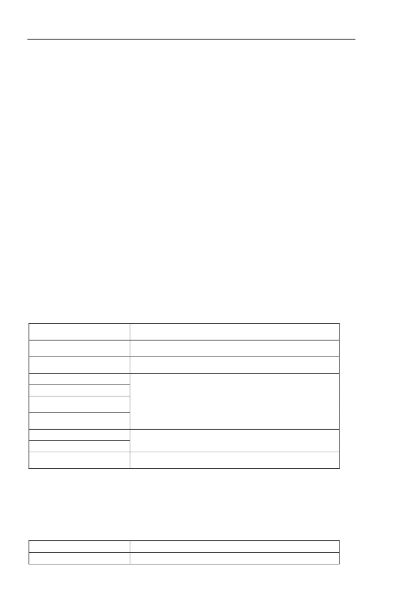
RTU frame format:
START
3.5-character time
Slave address ADDR
Communication address:1~247
Command code CMD
03:Read slaveparameters;06:Writeslaveparameters
DATA(N-1)
DATA(N-2)
Function code parameter address,function code parameter
………………………
number,function code parameter value,etc.
DATA0
CRC CHK loworder
Detection value:CRC value。
CRC CHK highorder
END
Atleast 3.5-character time
CMD(command instructions) and DATA(material words description)
Commandcode:03H,readsNwords(Thereare12characterscanberead atmost). For example:
the inverter start address F0.02 of the slave machine address 01 continuously reads two
consecutive values.
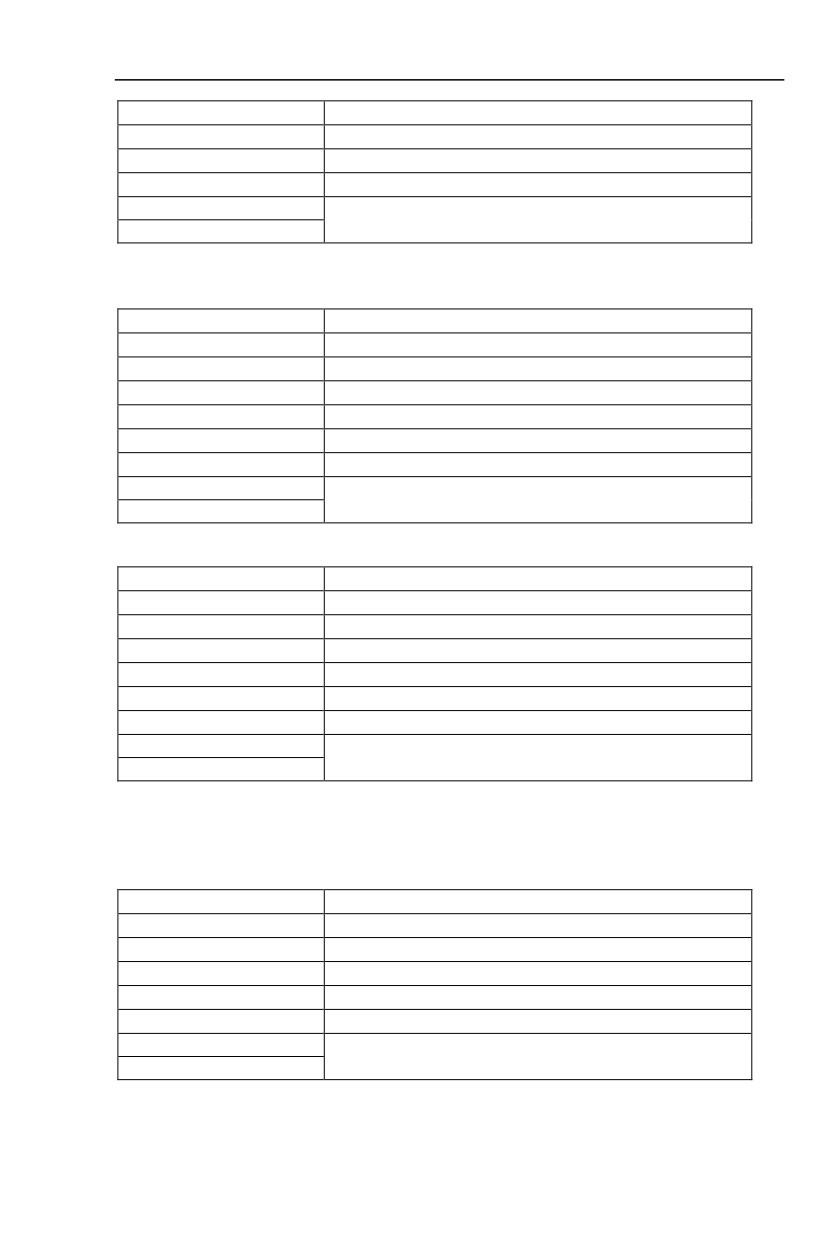
Host command
ADR
01H
CMD
03H
150
Appendix I
H5RS485 Card & RS485Communication Protocol
Start address highorder
F0H
Start address loworder
02H
Register number highorder
00H
Register number loworder
02H
CRC CHK low order
CRC CHK values to be calculated
CRC CHK high order
Slave response
PD.05=0:
ADR
01H
CMD
03H
Byte number high order
00H
Byte number low order
04H
Data P002H high order
00H
Data P002H low order
00H
Data P003H high order
01H
CRC CHK low order
CRC CHK values to be calculated
CRC CHK high order
PD.05=1:
ADR
01H
CMD
03H
Byte number
04H
Data F002H high order
00H
Data F002H low order
00H
Data F003H high order
00H
Data F003H low order
01H
CRC CHK low order
CRC CHK values to be calculated
CRC CHK high order
Command code:06H write a word
For example: Write 5000(1388H) into F00AH which slave address is 02H.
Master command information
ADR
02H
CMD
06H
Data address high order
F0H
Data address low order
0AH
Data content high order
13H
Data content low order
88H
CRC CHK low order
CRC CHK values to be calculated
CRC CHK high order
151

Appendix I H5RS485 Card & RS485Communication Protocol
Slave response
ADR
02H
CMD
06H
Data address high order
F0H
Data address low order
0AH
Data content high order
13H
Data content low order
88H
CRC CHK low order
CRC CHK values to be calculated
CRC CHK high order
I.4 Cyclical Redundancy Check
Cyclical Redundancy Check—CRC mode:CRC(Cyclical Redundancy Check) is in RTU
frame format, message contains an error-checking field that is based on a CRC method. The
CRC field checks the contents of the entire message. The CRC field is two bytes, containing a
16-bit binary value. The CRC value is calculated by the transmitting device, which appends the
CRC to the message. The receiving device recalculates a CRC during receipt of the message,
and compares the calculated value to the actual value it received in the CRC field. If the two
values are not equal, an error results. The CRC is started by 0xFFFF. Then a process begins of
applying successive 8-bit bytes of the message to the current contents of the register. Only the
eight bits of data in each character are used for generating the CRC. Start and stop bits, and the
parity bit, do not apply to the CRC.
During generation of the CRC, each eight-bit character is exclusive XOR with the register
contents. Then the result is shifted in the direction of the least significant bit (LSB), with a ZERO
filled into the most significant bit (MSB) position. The LSB extracted and examined. If the LSB
was 1, the register then exclusive XOR with a preset, fixed value. If the LSB was 0, no exclusive
XOR takes place. This process is repeated until 8 shifts have been performed. After the last (8)
shift, the next eight-bit byte is exclusive XOR with the register’s current value, and the process
repeats for 8 more shifts as described above. The final contents of the register, after all the
bytes of the message have been applied, is the CRC value.
When CRC appended to the message, the low byte is appended first, and then the high
byte.
CRC calculation program:
unsigned int cal_crc16
(unsigned char *data, unsigned int length)
{
unsigned int i,crc_result=0xffff;
while(length--)
{
crc_result^=*data++;
for(i=0;i<8;i++)
{
if(crc_result&0x01)
152
Appendix I H5RS485 Card & RS485Communication Protocol
crc_result=(crc_result>>1)^0xa001;
else
crc_result=crc_result>>1;
}
}
crc_result=((crc_result&0xff)<<8)|(crc_result>>8);
return(crc_result);
153
Appendix I H5RS485 Card & RS485Communication Protocol
I.5 Communication parameter address
The chapter is about communication contents, it’s used to control the inverter operation, the
status of the inverter and related parameter setup. Read and write functioncode parameters
(Some function codesare not able to be changed, only for the manufacturer use.). The mark
rules of function code parameters address:
The group number and mark of function codesare parameter address for indication rules.
High byte:F0~FF(P group), A0~AF(A group), 70~F(U group)Low byte:00~FF
For example: P3.12, the address indicates F30C
Caution:
Group PF: Parameters could not be read or be modified.
Group U: Parameters could be read but not be modified.
Some parameters can not be changed during operation, some parameters regardless of
the kind of state the inverter in, the parameters can not be changed. Change the function code
parameters, pay attention to the scope of the parameters, units, and relative instructions.
Besides, if EEPROM is frequently stored, it will reduce the service life of EEPROM. In some
communication mode, function code need to be stored as long as changing the RAM value.
Group P: to achieve this function, change high order F of the function code address into 0.
Group A: to achieve this function, change high order A of the function code address to be 4.
Corresponding function code address are indicated below:
High byte: 00~0F(P group), 40~4F(A group)Low byte: 00~FF
For example:
Function code P3.12 can not be stored into EEPROM, address indicates to be
030C,function code A0-05 can not be stored in EEPROM, address indicates to be 4005;This
address can only act writing RAM, it can not act reading, when act reading, it is invalid address.
For all parameters, command code 07H can be used to achieve this function.
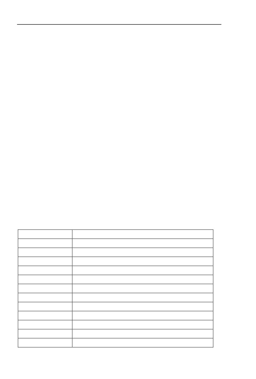
Stop/running parameter:
Parameter addr.
Parameter description
1000
* Communication setup value(-10000~10000)(Decimal)
1001
Running frequency
1002
Bus voltage
1003
Output voltage
1004
Output current
1005
Output power
1006
Output torque
1007
Running speed
1008
DI input status
1009
DO output status
100A
AI1voltage
100B
AI2 voltage
154
Appendix I H5RS485 Card & RS485Communication Protocol
100C
AI3 voltage
100D
Counting value input
100E
Length value input
100F
Load speed
1010
PID setup
1011
PID feedback
1012
PLC process
1013
PULSE input pulse frequency, unit 0.01kHz
1014
Feedback speed, unit 0.1Hz
1015
Rest running time
1016
AI1 voltage before correction
1017
AI2 voltage before correction
1018
AI3 voltage before correction
1019
Line speed
101A
Current power on time
101B
Current running time
101C
PULSE input pulse frequency, unit 1Hz
101D
Communication setup value
101E
Actual feedback speed
101F
Main frequency X display
1020
Auxiliary frequency Y display
Caution:
The communication setup value is percentage of the relative value, 10000 corresponds
to
100.00% , -10000 correspondsto
-100.00%.For data of dimensional frequency,the
percentage value is the percentage of the maximum frequency.For data of dimensional
torque, the percentage is P2.10, A2.48, A3.48, A4.48
(Torque upper digital setup,
corresponding to the first, second, third, fourth motor).
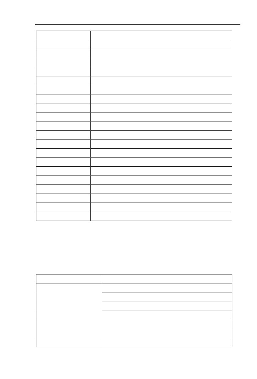
Control command input to the inverter (write-only)
Command word address
Command function
0001:Forward operation
0002:Reverse operation
0003:Forward jog
2000
0004:Reverse jog
0005:Free stop
0006:Speed-Down stop
0007:Fault reset
155
Appendix I H5RS485 Card & RS485Communication Protocol
Read inverter status:(read-only)
Status word address
Status word function
0001:Forward operation
3000
0002:Reverse operation
0003:Stop
Parameters lock password check:(if the return is the 8888H, it indicates the password
checksum pass)
Password address
Contents of input password
1F00
*****
Digital output terminal control:(write-only)
Command address
Command content
BIT0:DO1 Output control
BIT1:DO2 Output control
BIT2 RELAY1 Output control
BIT3:RELAY2 Output control
BIT4:Y1R Output control
2001
BIT5:VY1
BIT6:VY2
BIT7:VY3
BIT8:VY4
BIT9:VY5
Analog output AO1 control:(write-only)
Command address
Command content
2002
0~7FFF indicates 0%~100%
Analog output AO2control:(write-only)
Command address
Command content
2003
0~7FFFindicates 0%~100%
(PULSE)output control :(write-only)
Command address
Command content
2004
0~7FFFindicates 0%~100%
Inverter fault description:
Inverter fault address
Inverter fault information
0000:No fault
0001:Reserved
8000
0002:Speed-up over current
0003:Speed-down over current
156

Appendix I
H5RS485 Card & RS485Communication Protocol
0004:Constant speed over current
0005:Speed-up over voltage
0006:Speed-DOWN over voltage
0007:Constant speed over voltage
0008:Buffer resistance overload fault
0009:Under-voltage fault
000A:Inverter overload
000B:Motor overload
000C:Input phase lost
000D:Output phase lost
000E:Module overheating
000F:External fault
0010:Communication fault
0011:Contactor fault
0012:Current detection fault
0013:Motor tuning fault
0014:Encoder/PG card fault
0015:Parameter read and write fault
0016:Inverter hardware fault
0017:Motor earthing short-circuit fault
0018:Reserved
0019:Reserved
001A:Running time arrive fault
001B:User defined fault 1
001C:User defined fault 2
001D:Power on time arrive fault
001E:Load off
001F:PID feedback lost during operation
0028:Fast current limit timeout fault
0029:Motor shifting fault during operation
002A:Excessive speed deviation
002B:Motor over speed
002D:Motor over-temperature
005A:Encoder line number setup fault
005B:Encoder not connected
005C:Initial position error
005E:Speed feedback fault
Communication fault information describing data (fault code):
Communication fault address
Fault function description
0000:No fault
0001:Password error
0002:Command code error
0003:CRC check error
8001
0004:Invalid address
0005:Invalid parameter
0006:Parameter change invalid
0007:The system is locked
0008:Operating EEPROM
Pd group communication parameters description
Baud rate
Factory default value
6005
1 bit:MODUBS baud rate
0:300BPS
1:600BPS
Pd.00
2:1200BPS
3:2400BPS
Setup range
4:4800BPS
5:9600BPS
6:19200BPS
7:38400BPS
8:57600BPS
9:115200BPS
157
Appendix I H5RS485 Card & RS485Communication Protocol
This parameter is used to set the data transfer rate between the host computer and the
inverter. Caution:The baud rate of the position machine and the inverter must be consistent.
Or,communication is impossible.The higher the baud rate is,the faster the communication is.
Data format
Factory default value
0
0:No check:data format <8,N,2>
Pd.01
1:Even parity check:data format <8,E,1>
Setup range
2:Odd parity check:data format <8,O,1>
3:No check:data format <8-N-1>
The data format of the position machine and the inverter setup must be consistent,
Otherwise communication is impossible.
Local address
Factory default value
1
Pd.02
Setup range
1~247,0 is broadcast address.
When the local address is set to 0, that is the broadcast address, achieve position
machine’s broadcast function. The local address is unique (except for the broadcast address),
which is the basis for the position machine and the inverter point to point communication.
Response delay
Factory default value
2ms
Pd.03
Setup range
0~20ms
Response delay: It refers to the interval time from the inverter finishes receiving data to
sending data to the position machine. If the response delay is less than the system processing
time, then the response based on the time delay of the system processing time. If the response
delay is more than the system processing time, after the system process the data, it should be
delayed to wait until the response delay time is up, then sending data to host machine.
Communication
Factory default value
0.0 s
Overtime
Pd.04
0.0 s (Invalid)
Setup range
0.1~60.0s
When the function set to 0.0s, the communication overtime parameter is invalid.
When the function code is set to valid value, if the interval time between one
communication with the next communication exceeded the communications overtime, the
system will report communication fault error
(fault serial
16= E.CoF1) . Under normal
circumstances, it will be set to invalid value. If the system of continuous communication, setting
parameters, you can monitor the communication status.
Communication
Factory default value
0
protocol selection
Pd.05
0:Non standard Modbus protocol
Setup range
1:Standard Modbus protocol
158

Appendix I H5RS485 Card & RS485Communication Protocol
Pd.05=1:Select Standard Modbus protocol.
Pd.05=0:Reading command, the slave returns the number of bytes which has one more byte
than the standard Modbus protocol, for specific please refer to the protocol, the part of the "5
communication data structure”.
Communication
read the current
Factory default value
0
Pd.06
resolution
0:0.01A
Setup range
1:0.1A
To determine when the communication reads the output current, what the output current
value unit is.
159
Appendix II Parameter Settings List
Parameters factory default values are shown as below:
Code
Description/Display
Factory setting
Set value 1
Set value 2
U0
Monitor function group: U0.00-U0.61
U0.00
Running frequency
0.01Hz
U0.01
Set frequency
0.01Hz
U0.02
DC bus voltage
0.1V
U0.03
The output voltage
1V
U0.04
Motor output current
0.01A
U0.05
The output power
0.1kW
U0.06
Output torque
0.1%
U0.07
DI input status
1
U0.08
Y output status
1
U0.09
AI1 voltage
0.01V
U0.10
AI2 voltage
0.01V
U0.11
AI3 voltage
0.01V
U0.12
Count value
1
U0.13
Length value
1
U0.14
Load speed display
1
U0.15
PID set point
1
U0.16
PID feedback
1
U0.17
PLC stage
1
U0.18
PULSE pulse input frequency
0.01kHz
U0.19
Speed feedback
0.1Hz
U0.20
Surplus running time
0.1Min
U0.21
AI1 voltage before correction
0.001V
U0.22
AI2 voltage before correction
0.001V
U0.23
AI3 voltage before correction
0.001V
U0.24
Linear velocity
1m/Min
U0.25
Current power on time
1Min
U0.26
Current running time
0.1Min
U0.27
PULSE pulse input frequency
1Hz
U0.28
Communication set value
0.01%
U0.29
Encoder feedback speed
0.01Hz
160
Appendix II
Parameter Settings List
U0.30
Main frequency X display
0.01Hz
U0.31
Auxiliary frequency Y display
0.01Hz
U0.32
View arbitrary memory address
1
U0.33
Synchronous motor rotor position
0.0°
U0.34
Motor temperature
1ć
U0.35
Target torque
0.1%
U0.36
Rotary variable position
1
U0.37
Power factor angle
0.1
U0.38
ABZ position
0.0
U0.39
VF target voltage separation
1V
U0.40
VF output voltage separation
1V
U0.41
DI input status intuitive display
-
U0.42
DO output status intuitive display
-
U0.43
DI function status intuitive display1
1
U0.44
DI function status intuitive display2
1
U0.45
Fault information
0
U0.46
Reserved
-
U0.47
Reserved
-
U0.48
Reserved
-
U0.58
Z signal counter
-
U0.59
Set frequency
0.01%
U0.60
Running frequency
0.01%
U0.61
Inverter status
1
U0.62
Current fault code
1
U0.63
Point to point communication
0.01%
U0.64
number of Slave
1
U0.65
Torque limit
0.01%
P0
Basic function group:P0.00-P0.28
P0.00
GP type display
-
P0.01
Motor 1 control mode
0
P0.02
Command source selection
0
P0.03
Main frequency source X selection
4
P0.04
Auxiliary frequencysource Y selection
0
P0.05
Auxiliary frequency source Y range selection
0
P0.06
Auxiliary frequency source Y range
100%
161
Appendix II Parameter Settings List
P0.07
Frequency source stacking selection
00
P0.08
Preset frequency
50.00Hz
P0.09
Running direction
0
P0.10
Maximum frequency
50.00Hz
P0.11
Frequency source upper limit
0
P0.12
Frequency upper limit
50.00Hz
P0.13
Frequency upper limit offset
0.00Hz
P0.14
Frequency lower limit
0.00Hz
P0.15
Carrier frequency
-
P0.16
Carrier frequency adjusting with temperature
0
P0.17
Acceleration time 1
-
P0.18
Deceleration time 1
-
P0.19
Acc./ dec. time unit
1
P0.21
Auxiliary frequency source offset frequency
0.00Hz
P0.22
Frequency command resolution
2
P0.23
Digital setup frequency memory selection upon stop
0
P0.24
Motor selection
0
P0.25
Acceleration / deceleration reference frequency
0
P0.26
Frequency UP/DOWNreference upon running
0
P0.27
Command source& frequency source binding
000
P0.28
Communication expansion card
0
P1
Parameters for motor 1: P1.00-P0.37
P1.00
Motor type selection
0
P1.01
Rated power
-
P1.02
Rated voltage
-
P1.03
Rated current
-
P1.04
Rated frequency
-
P1.05
Rated revolving speed
-
P1.06
Asynchronous motor stator resistance
-
P1.07
Asynchronous motor rotor resistance
-
P1.08
Asynchronous motor leakage inductance
-
P1.09
Asynchronous motor mutual inductance
-
P1.10
Asynchronous motor no load current
-
P1.27
Encoder pulses number
2500
P1.28
Encoder type
0
162
Appendix II Parameter Settings List
P1.30
ABZ incremental encoder AB phase
0
P1.31
Encoder installation angle
0.00
P1.32
UVW phase sequence
0
P1.33
UVW encoder offset angle
0.00
P1.34
Rotary transformer pole pairs
1
P1.35
UVW pole-pairs
4
P1.36
PG dropped inspection time
0.0s
P1.37
Tuning selection
0
P2
Vector control function group: P2.00-P2.22
P2.00
Speed loop proportional gain 1
30
P2.01
Speed loop integration time1
0.50s
P2.02
Switching frequency1
5.00Hz
P2.03
Speed loop proportional gain 2
20
P2.04
Speed loop integration time 2
1.00s
P2.05
Switching frequency 2
10.00Hz
P2.06
Vector control slip gain
100%
P2.07
Speed-loop filter time
28
P2.08
Vector control over-excitation gain
64
P2.09
Torque upper limit source in speed control mode
0
Torque upper limit digital setup in speed control
P2.10
150.0%
mode
P2.13
Excitation regulation proportional gain
2000
P2.14
Excitation regulation integration gain
1300
P2.15
Torque regulation proportional gain
2000
P2.16
Torque regulation integration gain
1300
P2.17
Speed loop integration attribute
0
P2.18
Synchronous motor field weakening mode
1
P2.19
Synchronous motor field weakening depth
100%
P2.20
Maximum field weakening current
50%
P2.21
Field weakening auto regulation gain
100%
P2.22
Field weakening integration multiples
2
P3
V/F control group: P3.00-P3.15
P3.00
V/F curve setup
0
P3.01
Torque boost value
-
163
Appendix II
Parameter Settings List
P3.02
Torque boost cut-off frequency
50.00Hz
P3.03
Multi-point V/F frequency point F1
0.00Hz
P3.04
Multi-point V/F voltage point V1
0.0%
P3.05
Multi-point V/F frequency point F2
0.00Hz
P3.06
Multi-point V/F voltage point V2
0.0%
P3.07
Multi-point V/F frequency point F3
0.00Hz
P3.08
Multi-point V/F voltage point V3
0.0%
P3.09
V/F slip compensation gain
0.0%
P3.10
VF over-excitation gain
64
P3.11
VF oscillation suppression gain
-
P3.13
VF separation voltage source
0
P3.14
VF separation voltage digital setup
0V
P3.15
VF separation voltage rise time
0.0s
P4
Input Terminal: P4.00-P4.39
P4.00
DI1terminal function selection
1
P4.01
DI2 terminal function selection
4
P4.02
DI3 terminal function selection
9
P4.03
DI4 terminal function selection
12
P4.04
DI5 terminal function selection
0
P4.05
DI6 terminal function selection
0
0
P4.06
DI7 terminal function selection
0
P4.07
DI8 terminal function selection
0
P4.08
DI9 terminal function selection
0
P4.09
DI10 terminal function selection
P4.10
DI filter time
0.010s
P4.11
Terminal command mode
0
P4.12
Terminal UP/DN variation rate
1.00Hz/s
P4.13
AI curve 1 minimum input
0.00V
P4.14
AI curve 1 minimum input corresponding setup
0.0%
P4.15
AI curve 1 maximum input
10.00V
P4.16
AI curve 1 maximum input corresponding setup
100.0%
P4.17
AI1 filter time
0.10s
P4.18
AI curve 2 minimum input
0.00V
164
Appendix II Parameter Settings List
P4.19
AI curve 2 minimum input corresponding setup
0.0%
P4.20
AI curve 2 maximum input
10.00V
P4.21
AI curve 2 maximum input corresponding setup
100.0%
P4.22
AI2 filter time
0.10s
P4.23
AI curve 3 minimum input
0.10V
P4.24
AI curve 3 minimum input corresponding setup
0.0%
P4.25
AI curve3 maximum input
4.00V
P4.26
AI curve 3 maximum input corresponding setup
100.0%
P4.27
AI3filter time
0.10s
P4.28
PULSE minimum input
0.00kHz
P4.29
PULSE minimum input corresponding setup
0.0%
P4.30
PULSE maximum input
50.00
P4.31
PULSE maximum input corresponding setup
100.0%
P4.32
PULSE filter time
0.10s
P4.33
AI curve selection
321
P4.34
AI below minimum input setup selection
000
P4.35
DI1 delay time
0.0s
P4.36
DI2 delay time
0.0s
P4.37
DI3 delay time
0.0s
P4.38
DI terminal effective mode selection 1
00000
P4.39
DI terminal effective mode selection 2
00000
P5
Output terminal: P5.00-P5.22
P5.00
Y1 terminal output mode selection
0
P5.01
Y1R selection (open collector output terminal )
0
P5.02
Relay output selection(TA1.TB1.TC1)
2
P5.03
Expansion card relay output selection(TA2.TB2.TC2)
0
P5.04
DO1 output selection(open collector output terminal)
1
P5.05
Expansion cardDO2 output selection
4
P5.06
Y1P output selection (pulse output terminal)
0
P5.07
AO1 output selection
0
P5.08
AO2 output selection
1
P5.09
Y1P maximum output frequency
50.00kHz
P5.10
AO1 zero offset
0.0%
165
Appendix II Parameter Settings List
P5.11
AO1 gain
1.00
P5.12
AO2 zero offset
0.00%
P5.13
AO2 gain
1.00
P5.17
Y1R output delay time
0.0s
P5.18
RELAY1 output delay time
0.0s
P5.19
RELAY2 output delay time
0.0s
P5.20
DO1 output delay time
0.0s
P5.21
DO2 output delay time
0.0s
P5.22
DO output terminal valid state selection
00000
P6
Start/stop control: P6.00-P6.15
P6.00
Start mode
0
P6.01
Revolving speed tracking mode
0
P6.02
Revolving speed tracking speed
20
P6.03
Start frequency
0.00Hz
P6.04
Start frequency holding time
0.0s
P6.05
Start dc braking current /pre-excitation current
0%
P6.06
Start dc braking time /pre-excitation time
0.0s
P6.07
Acceleration/deceleration mode
0
P6.08
S-curve initial-segment time proportion
30.0%
P6.09
S-curve end-segment time proportion
30.0%
P6.10
Stop mode
0
P6.11
DC braking initial frequency at stop
0.00Hz
P6.12
DC braking waiting time at stop
0.0s
P6.13
DC braking current at stop
0%
P6.14
DC braking time at stop
0.0s
P6.15
Brake utilization ratio
100%
P7
Keyboard and display: P7.00-P7.14
P7.01
MF/REV key function selection
0
P7.02
STOP/RESET function
1
P7.03
LED running display parameter 1
1F
P7.04
LED running display parameter 2
0
P7.05
LED stop display parameter
0
P7.06
Load speed coefficient
1.0000
P7.07
Inverter module radiator temperature
166
Appendix II
Parameter Settings List
P7.08
product ID
P7.09
Accumulative running time
0h
P7.10
Performance version number
-
P7.11
Software version No.
-
P7.12
Load speed display decimal digits
1
P7.13
Accumulative power-on time
-
P7.14
Accumulative power consumption
-
P8
Auxiliary Function: P8.00-P8.53
P8.00
Jog running frequency
2.00Hz
P8.01
Jog acceleration time
20.0s
P8.02
Jog deceleration time
20.0s
P8.03
Acceleration time 2
10.0s
P8.04
Deceleration time 2
10.0s
P8.05
Acceleration time 3
10.0s
P8.06
Deceleration time 3
10.0s
P8.07
Acceleration time 4
10.0s
P8.08
Deceleration time 4
10.0s
P8.09
Hopping frequency 1
0.00Hz
P8.10
Hopping frequency 2
0.00Hz
P8.11
Hopping frequency amplitude
0.00Hz
P8.12
Dead zone time of forward & reverse rotations
0.0s
P8.13
Reverse rotation control
0
P8.14
Set frequency below lower limit running mode
0
P8.15
Droop control
0.00Hz
P8.16
Accumulative power-on time arrival setup
0h
P8.17
Accumulative running time arrival setup
0h
P8.18
Start protection selection
0
P8.19
Frequency detection value (FDT1)
50.00Hz
P8.20
Frequency detection hysteresis value (FDT1)
5.0%
P8.21
Frequency arrival detection amplitude
0.0%
P8.22
Acc./dec. hopping frequency validity
0
P8.25
Acc. time1 & acc. time 2 frequency switching point
0.00Hz
P8.26
Dec. time1 & dec. time 2 frequency switching point
0.00Hz
P8.27
Terminal jog priority
0
167
Appendix II Parameter Settings List
P8.28
Frequency detection value(FDT2)
50.00Hz
P8.29
Frequency detection hysteresis value(FDT2)
5.0%
P8.30
Random frequency arrival detection value1
50.00Hz
P8.31
Random frequency arrival detection range1
0.0%
P8.32
Random frequency arrival detection value2
50.00Hz
P8.33
Random frequency arrival detection range2
0.0%
P8.34
Zero-current detection level
5.0%
P8.35
Zero-current detection delay time
0.10s
P8.36
Output current overlimit value
200.0%
P8.37
Output current overlimit detection delay time
0.00s
P8.38
Random current arrival 1
100.0%
P8.39
Random current arrival range1
0.0%
P8.40
Random current arrival 2
100.0%
P8.41
Random current arrival range2
0.0%
P8.42
Timing function selection
0
P8.43
Running time timing selection
0
P8.44
Timing running time
0.0Min
P8.45
AI1 input voltage protection value lower limit
3.10V
6.80V
P8.46
AI1 input voltage protection value upper limit
P8.47
Module temperature arrival
75ć
P8.48
Cooling fan control
0
P8.49
Wake-up frequency
0.00Hz
P8.50
Wake-up delay time
0.0s
P8.51
Sleep frequency
0.00Hz
P8.52
Sleep delay time
0.0s
P8.53
The running time arrival
0.0Min
P9
Overload and Protection: P9.00-P9.70
P9.00
Motor overload protection selection
1
P9.01
Motor overload protection gain
1.00
P9.02
Motor overload pre-alarm coefficient
80%
P9.03
Over-voltage stall gain
0
P9.04
Over-voltage stall protection voltage
130%
P9.05
Over current stall gain
20
168
Appendix II Parameter Settings List
P9.06
Over current stall protection current
150%
P9.07
Ground short circuit protection upon power-on
1
P9.09
Fault auto reset times
0
P9.10
Fault auto reset FAULT DO selection
0
P9.11
Fault auto reset interval
1.0s
P9.12
Input phase lack protection selection
11
P9.13
Output phase lack protection selection
1
P9.14
The first fault type
-
P9.15
The second fault type
-
P9.16
The latest fault type
-
P9.17
Third fault frequency
-
P9.18
Third fault current
-
P9.19
Third fault bus voltage
-
P9.20
Third fault input terminal
-
P9.21
Third fault output terminal
-
P9.22
Third fault inverter state
-
P9.23
Third fault power-on time
-
P9.24
Third fault running time
-
P9.27
Second fault frequency
-
P9.28
Second fault current
-
P9.29
Second fault bus voltage
-
P9.30
Second fault input terminal
-
P9.31
Second fault output terminal
-
P9.32
Second fault inverter state
-
P9.33
Second fault power-on time
-
P9.34
Second fault running time
-
P9.37
First fault frequency
-
P9.38
First fault current
-
P9.39
First fault bus voltage
-
P9.40
First fault input terminal
-
P9.41
First fault output terminal
-
P9.42
First fault inverter state
-
P9.43
First fault power-on time
-
P9.44
First fault running time
-
169
Appendix II Parameter Settings List
P9.47
Fault protection action selection 1
00000
P9.48
Fault protection action selection 2
00000
P9.49
Fault protection action selection 3
00000
P9.50
Fault protection action selection 4
00000
P9.54
Continued to run when fault frequency selection
0
P9.55
Abnormal backup frequency
100.0%
P9.56
Motor temperature sensor
0
P9.57
Motor overheating protection threshold
110ć
P9.58
Motor overheating pre-alarm threshold
90ć
P9.59
Transient stop selection
0
P9.60
Transient stop action pause protection voltage
90.0%
P9.61
Transient stop voltage recovery judgment time
0.50s
P9.62
Transient stop action judgment voltage
80.0%
P9.63
Load-off protection selection
0
P9.64
Load-off detection level
10.0%
P9.65
Load-off detection time
1.0s
P9.67
Over speed detection value
20.0%
P9.68
Over speed detection time
1.0s
P9.69
Excessive speed deviation detection value
20.0%
P9.70
Excessive speed deviation detection time
5.0s
PA
PID Function group: PA.00-PA.28
PA.00
PID reference source
0
PA.01
PID reference value
50.0%
PA.02
PID feedback source
0
PA.03
PID action direction
0
PA.04
PID reference feedback range
1000
PA.05
Proportional gain Kp1
20.0
PA.06
Integration time Ti1
2.00s
PA.07
Differential time Td1
0.000s
PA.08
PID cutoff frequency of reverse rotation
2.00Hz
PA.09
PID deviation limit
0.0%
PA.10
PID differential amplitude limit
0.10%
PA.11
PID reference change duration
0.00s
PA.12
PID feedback filter time
0.00s
170
Appendix II Parameter Settings List
PA.13
PID output filter time
0.00s
PA.14
Reserved
-
PA.15
Proportional gain Kp2
20.0
PA.16
Integration time Ti2
2.00s
PA.17
Differential time Td2
0.000s
PA.18
PID parameter switching condition
0
PA.19
PID parameter switching deviation1
20.0%
PA.20
PID parameter switching deviation2
80.0%
PA.21
PID initial value
0.0%
PA.22
PID initial value retention time
0.00s
PA.23
Output deviation forward maximum value
1.00%
PA.24
Output deviation reverse maximum value
1.00%
PA.25
PID integration attribute
00
PA.26
PID feedback loss detection value
0.0%
PA.27
PID feedback loss detection time
0s
PA.28
PID stop operation
0
Pb
Swing Frequency, Fixed Length and Counting: Pb.00-Pb.09
Pb.00
Swing setup mode
0
Pb.01
Swing frequency amplitude
0.0%
Pb.02
Jump frequency amplitude
0.0%
Pb.03
Swing frequency cycle
10.0s
Pb.04
Triangle wave rise time coefficient
50.0%
Pb.05
Setup length
1000m
Pb.06
Actual length
0m
Pb.07
Pulse number per meter
100.0
Pb.08
Counting value setup
1000
Pb.09
Designated counting value
1000
PC
MS Speed Function & Simple PLC Function: PC.00-PC.51
PC.00
MS command 0
0.0%
PC.01
MS command 1
0.0%
PC.02
MS command 2
0.0%
PC.03
MS command 3
0.0%
PC.04
MS command 4
0.0%
171
Appendix II
Parameter Settings List
PC.05
MS command 5
0.0%
PC.06
MS command 6
0.0%
PC.07
MS command 7
0.0%
PC.08
MS command 8
0.0%
PC.09
MS command 9
0.0%
PC.10
MS command 10
0.0%
PC.11
MS command 11
0.0%
PC.12
MS command 12
0.0%
PC.13
MS command 13
0.0%
PC.14
MS command 14
0.0%
PC.15
MS command 15
0.0%
PC.16
PLC running mode
0
PC.17
PLC power off memory selection
00
PC.18
PLC 0segment running time
0.0s(h)
PC.19
PLC 0segment acc./dec. time
0
PC.20
PLC 1segment running time
0.0s(h)
PC.21
PLC 1segment acc./dec. time
0
PC.22
PLC 2 segment running time
0.0s(h)
PC.23
PLC 2 segment acc./dec. time
0
PC.24
PLC 3 segment running time
0.0s(h)
PC.25
PLC 3 segment acc./dec. time
0
PC.26
PLC 4 segment running time
0.0s(h)
PC.27
PLC 4 segment acc./dec. time
0
PC.28
PLC 5 segment running time
0.0s(h)
PC.29
PLC 5 segment acc./dec. time
0
PC.30
PLC 6 segment running time
0.0s(h)
PC.31
PLC 6 segment acc./dec. time
0
PC.32
PLC 7 segment running time
0.0s(h)
PC.33
PLC 7 segment acc./dec. time
0
PC.34
PLC 8 segment running time
0.0s(h)
PC.35
PLC 8 segment acc./dec. time
0
PC.36
PLC 9 segment running time
0.0s(h)
PC.37
PLC 9 segment acc./dec. time
0
172
Appendix II Parameter Settings List
PC.38
PLC 10 segment running time
0.0s(h)
PC.39
PLC 10 segment acc./dec. time
0
PC.40
PLC 11 segment running time
0.0s(h)
PC.41
PLC 11 segment acc./dec. time
0
PC.42
PLC 12 segment running time
0.0s(h)
PC.43
PLC 12 segment acc./dec. time
0
PC.44
PLC 13 segment running time
0.0s(h)
PC.45
PLC 13 segment acc./dec. time
0
PC.46
PLC 14 segment running time
0.0s(h)
PC.47
PLC 14 segment acc./dec. time
0
PC.48
PLC 15 segment running time
0.0s(h)
PC.49
PLC 15 segment acc./dec. time
0
PC.50
Running time unit
0
PC.51
MS command 0 reference mode
0
Pd
Communication function group:Pd.00-Pd.29
Pd.00
Baud rate
6005
Pd.01
Data format
0
Pd.02
Local address
1
Pd.03
Response delay
2
Pd.04
Excessive communication time
0.0
Pd.05
Data transformat selection
30
Pd.06
Communication read current resolution
0
PE
User customization function code: PE.00-PE.29
PE.00
User function code 0
P0.01
PE.01
User function code 1
P0.02
PE.02
User function code 2
P0.03
PE.03
User function code 3
P0.07
PE.04
User function code 4
P0.08
PE.05
User function code 5
P0.17
PE.06
User function code 6
P0.18
PE.07
User function code 7
P3.00
PE.08
User function code 8
P3.01
PE.09
User function code 9
P4.00
173
Appendix II
Parameter Settings List
PE.10
User function code 10
P4.01
PE.11
User function code 11
P4.02
PE.12
User function code 12
P5.04
PE.13
User function code 13
P5.07
PE.14
User function code 14
P6.00
PE.15
User function code 15
P6.10
PE.16
User function code 16
P0.00
PE.17
User function code 17
P0.00
PE.18
User function code 18
P0.00
PE.19
User function code 19
P0.00
PE.20
User function code 20
P0.00
PE.21
User function code 21
P0.00
PE.22
User function code 22
P0.00
PE.23
User function code 23
P0.00
PE.24
User function code 24
P0.00
PE.25
User function code 25
P0.00
PE.26
User function code 26
P0.00
PE.27
User function code 27
P0.00
PE.28
User function code 28
P0.00
PE.29
User function code 29
P0.00
PP
Function code management: PP.00-PP.04
PP.00
User password
0
PP.01
Parameter initialization
0
PP.02
Parameter display attribute
11
PP.03
Personalized parameter display selection
00
PP.04
Function codes modification attribute
0
A0
Torque control group: A0.00-A0.08
A0.00
Speed/ torque control mode selection
0
A0.01
Torque setup source selection in torque control mode
0
A0.03
Torque digital setup in torque control mode
150%
A0.05
Torque control forward maximum frequency
50.00Hz
A0.06
Torque control reverse maximum frequency
50.00Hz
A0.07
Torque control acc. time
0.00s
A0.08
Torque control dec. time
0.00s
174
Appendix II Parameter Settings List
A1
Virtual IO: A1.00-A1.21
A1.00
Virtual VDI1 function selection
0
A1.01
Virtual VDI2 function selection
0
A1.02
Virtual VDI3 function selection
0
A1.03
Virtual VDI4 function selection
0
A1.04
Virtual VDI5 function selection
0
A1.05
Virtual VD1 terminal valid state set mode
00000
A1.06
Virtual VD1 terminal state
00000
A1.07
AI1 as DI function selection
0
A1.08
AI2 as DI function selection
0
A1.09
AI3 as DI function selection
0
A1.10
AI as DI valid mode selection
000
A1.11
Virtual VDO1 output function
0
A1.12
Virtual VDO2 output function
0
A1.13
Virtual VDO3 output function
0
A1.14
Virtual VDO4 output function
0
A1.15
Virtual VDO5 output function
0
A1.16
VDO1 output delay time
0.0s
A1.17
VDO2 output delay time
0.0s
A1.18
VDO3 output delay time
0.0s
A1.19
VDO4 output delay time
0.0s
A1.20
VDO5 output delay time
0.0s
A1.21
VDO output terminal valid state selection
00000
A2
The second motor control: A2.00-A2.65
A2.00
Motor type selection
0
A2.01
Rated power
-
A2.02
Rated voltage
-
A2.03
Rated current
-
A2.04
Rated frequency
-
A2.05
Rated revolving speed
-
A2.06
Asynchronous motor stator resistance
-
A2.07
Asynchronous motor rotor resistance
-
A2.08
Asynchronous motor leakage inductance
-
175
Appendix II Parameter Settings List
A2.09
Asynchronous motor mutual inductance
-
A2.10
Asynchronous motor no load current
-
A2.16
Synchronous motor stator resistance
-
A2.17
Synchronous motor D-axis inductance
-
A2.18
Synchronous motor Q-axis inductance
-
Synchronous motor
A2.19
0
inductance resistance unit
Synchronous motor back electromotive force
A2.20
0.1V
coefficient.
Synchronous motor output phase lack
A2.21
0
detection time
A2.27
Encoder pulses number
2500
A2.28
Encoder type
0
A2.29
Speed feedback PG selection
0
A2.30
ABZ incremental encoder AB phase
0
A2.31
Encoder installation angle
0
A2.32
UVW phase sequence
0
A2.33
UVW encoder offset angle
0.00
A2.34
Rotary transformer pole pairs
1
A2.35
UVW pole-pairs
4
A2.36
PG dropped inspection time
0.0s
A2.37
Tuning selection
0
A2.38
Speed loop proportional gain 1
30
A2.39
Speed loop integration time1
0.50s
A2.40
Switching frequency1
5.00Hz
A2.41
Speed loop proportional gain 2
20
A2.42
Speed loop integration time 2
1.00s
A2.43
Switching frequency 2
10.00Hz
A2.44
Vector control slip gain
150%
A2.45
Speed-loop filtering time
0.000s
A2.46
Vector control over-excitation gain
64
Torque upper limit source in speed control
A2.47
0
mode
Torque upper limit digital setup in speed
A2.48
150.0%
control mode
A2.51
Excitation regulation proportional gain
2000
176
Appendix II Parameter Settings List
A2.52
Excitation regulation integration gain
1300
A2.53
Torque regulation proportional gain
2000
A2.54
Torque regulation integration gain
1300
A2.55
Speed loop integration attribute
0
A2.56
Synchronous motor field weakening mode
1
A2.57
Synchronous motor field weakening depth
100%
A2.58
Maximum field weakening current
50%
A2.59
Field weakening auto regulation gain
100%
A2.60
Field weakening integration multiples
2
A2.61
Motor2 control mode
0
A2.62
Motor 2 acc./dec. time selection
0
A2.63
Motor 2 torque hoist
-
A2.65
Motor 2 oscillation suppression gain
-
A5
Control optimization group:A5.00-A5.09
A5.00
DPWM switching frequency upper limit
12.00Hz
A5.01
PWM modulation mode
0
A5.02
Dead-zone compensation mode selection
1
A5.03
Random PWM depth
0
A5.04
Rapid current-limiting enable
1
A5.05
Current detection compensation
5
A5.06
Under-voltage point setup
100.0%
A5.07
SVC optimization mode selection
1
A5.08
Dead zone time adjustment
150%
A5.09
Over-voltage point setup
Model determination
A6
AI curve setup: A6.00-A6.29
A6.00
AI curve 4 minimum input
0.00V
AI curve 4 minimum input corresponding
A6.01
0.0%
setup
A6.02
AI curve 4inflection point 1 input
3.00V
AI curve 4 inflection point 1 input
A6.03
30.0%
corresponding setup
A6.04
AI curve 4 inflection point 2 input
6.00V
AI curve 4 inflection point 2 input
A6.05
60.0%
corresponding setup
A6.06
AI curve 4 maximum input
10.00V
AI curve 4 maximum input corresponding
A6.07
100.0%
setup
177
Appendix II Parameter Settings List
A6.08
AI curve 4 minimum input
-10.00V
AI curve 5 minimum input corresponding
A6.09
-100.0%
setup
A6.10
AI curve 5 inflection point 1 input
-3.00V
AI curve 5 inflection point 1 input
A6.11
-30.0%
corresponding setup
A6.12
AI curve 5 inflection point 2 input
3.00V
AI curve 5 inflection point 2 input
A6.13
30.0%
corresponding setup
A6.14
AI curve 5 maximum input
10.00V
AI curve 5 maximum input corresponding
A6.15
100.0%
setup
A6.24
AI1 set hopping point
0.0%
A6.25
AI1 set hopping amplitude
0.5%
A6.26
AI2 set hopping point
0.0%
A6.27
AI2 set hopping amplitude
0.5%
A6.28
AI3 set hopping point
0.0%
A6.29
AI3 set hopping amplitude
0.5%
A7
User programmable card parameters: A7.00-A7.09
A7.00
User programmable function selection
0
Control board output terminal control mode
A7.01
-
selection
Programmable card expansion AI3x function
A7.02
-
configuration
A7.03
Y1P output
0.0%
A7.04
AO1 output
0.0%
A7.05
Switch output
000
A7.06
Programmable card frequency setup
0.0%
A7.07
Programmable card torque setup
0.0%
A7.08
Programmable card command setup
0
A7.09
Programmable card fault setup
0
A8
Point to point communication:A8.00-8.11
A8.00
Master slave control function selection
0
A8.01
Master slave selection
0
A8.02
Master slave information exchange
011
A8.03
Message frame selection
0
A8.04
Receive data zero offset torque
0.00%
A8.05
Receive data gain torque
1.00
A8.06
Communication interrupt detection time
1.0s
178
Appendix II Parameter Settings List
Communication Master data transmission
A8.07
0.001s
cycle
A8.08
Receive data zero offset frequency
0.00%
A8.09
Receive data gain frequency
1.00
A8.10
Reverse
A8.11
view
0.5Hz
A9
Extended function group:A9.00-A9.09
A9.00
0
A9.01
0
A9.02
0
A9.03
0
A9.04
0
A9.05
0
A9.06
0
A9.07
0
A9.08
0
A9.09
0
AC
AIAO correction: AC.00-AC.19
AC.00
AI1measured voltage 1
Factory calibration
AC.01
AI1 display voltage 1
Factory calibration
AC.02
AI1 measured voltage 2
Factory calibration
AC.03
AI1 display voltage 2
Factory calibration
AC.04
AI2 measured voltage 1
Factory calibration
AC.05
AI2 display voltage 1
Factory calibration
AC.06
AI2 measured voltage 2
Factory calibration
AC.07
AI2 display voltage 2
Factory calibration
AC.08
AI3 measured voltage 1
Factory calibration
AC.09
AI3 display voltage 1
Factory calibration
AC.10
AI3 measured voltage 2
Factory calibration
AC.11
AI3 display voltage 2
Factory calibration
AC.12
A01 target voltage 1
Factory calibration
AC.13
A01 measured voltage 1
Factory calibration
AC.14
A01 target voltage 2
Factory calibration
AC.15
A01 measured voltage 2
Factory calibration
AC.16
A02 target voltage 1
Factory calibration
179

Appendix II Parameter Settings List
AC.17
A02 measured voltage 1
Factory calibration
AC.18
A02 target voltage 2
Factory calibration
AC.19
A02 measured voltage 2
Factory calibration
180