HV610-DP card. User manual
(86)
1. Overview
Thank you for using HV610 series inverter and choosing HV610-DP card!
The HV610-DP card is a Profibus-DP fieldbus adapter card, which conforms to the internationally
accepted Profibus fieldbus standard. The card is installed on the HV610 inverter to improve
communication efficiency and facilitate the networking function of the inverter. Make the inverter a
slave of the fieldbus and accept the control of the fieldbus master.
HV610-DP card can realize Profibus-DP communication.
Please read this manual carefully before using this product.
2. Installation and wiring
The HV610-DPcard is designed to be used in HV610 series inverters. Please turn off the power
supply to the inverter before installation. Wait for about 10 minutes before the inverter's charging
indicator goes out before installation. After the HV610-DP card is inserted into the inverter, please
fix the corresponding screws to prevent the signal socket between the boards from being damaged
by the external signal cable.
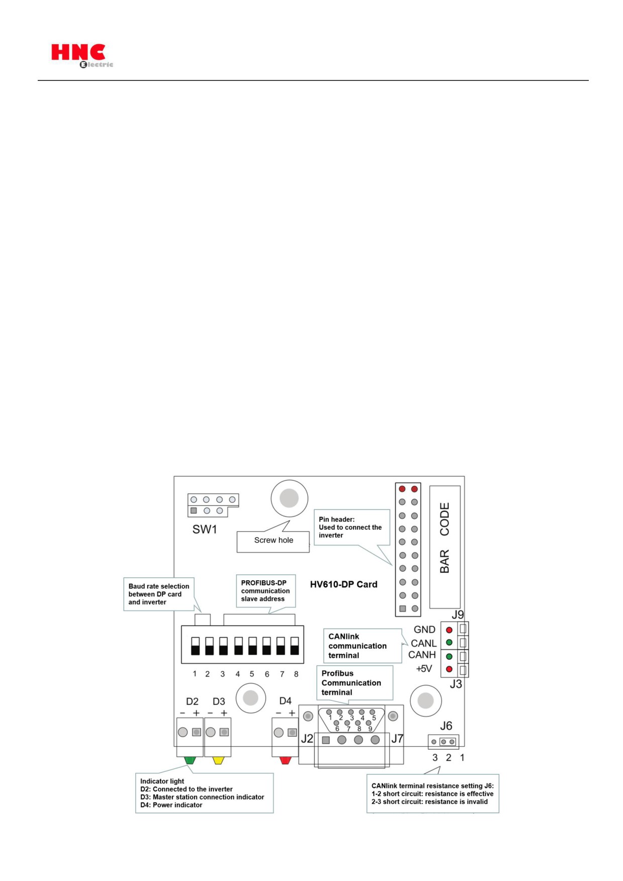
Card hardware layout
Figure 1 Terminal distribution of HV610-DP card
(86)
DIP switch description
Bit
Function
Description
1
DP card ON/OFF
OFF: HV610-DP is invalid
ON: HV610-DP is valid
2
Reserved
Reserved
3~8
Profibus-DP
Bit 3 ~ Bit 8 six-digit binary DIP switch can set station address 0~63.
communication
Example:
Bit 3 ~ Bit 8
Local Address
slave address
00 0000
Fd-02 decision
00 0111
07
01 0100
20
(Note: When the DIP switch is set to 0, the local address is set by the HV610
inverter function code Fd-03)
Note:
This HV610-DP only supports a communication rate of 115.2K with the inverter, that is, the tens
digit of Fd-01 needs to be set to 0; the version information of the card cannot be viewed when using
HV610-DP; changing the dial bit number 1, you need to power on again the inverter to take effect.
Interface Description
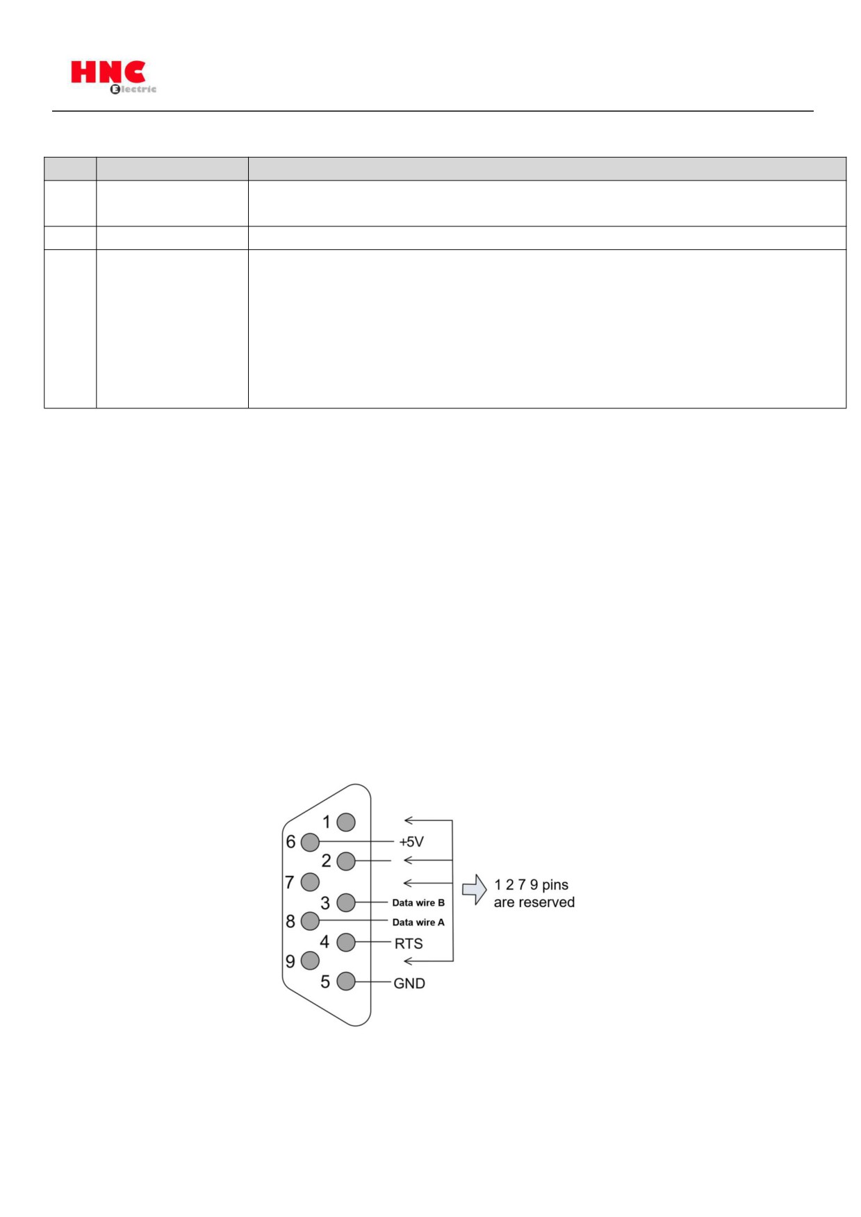
Profibus DB9 interface description
The HV610-DP card uses a standard DB9 socket to connect to the Profibus master station, and its
pin signal definition is in accordance with the DB9 socket standard distribution of SIEMENS.
As shown below:
Figure 2 DB9 interface pin function description
(86)
Control terminal function description
Type
Terminal
Terminal name
Function
1/2/7/9
NC
No connect (reserved)
3
Data wire B
Data wire B (+)
Profibus-DP
4
RTS
Request to send a signal
Communication
5
GND
Isolated 5V Power Ground
terminal (J2)
6
+5V
Isolated 5V Power +5V
8
Data wire A
Data wire A (-)
Manufacturer debugging interface, users should
Factory reserved
SWI
Reserved
not use
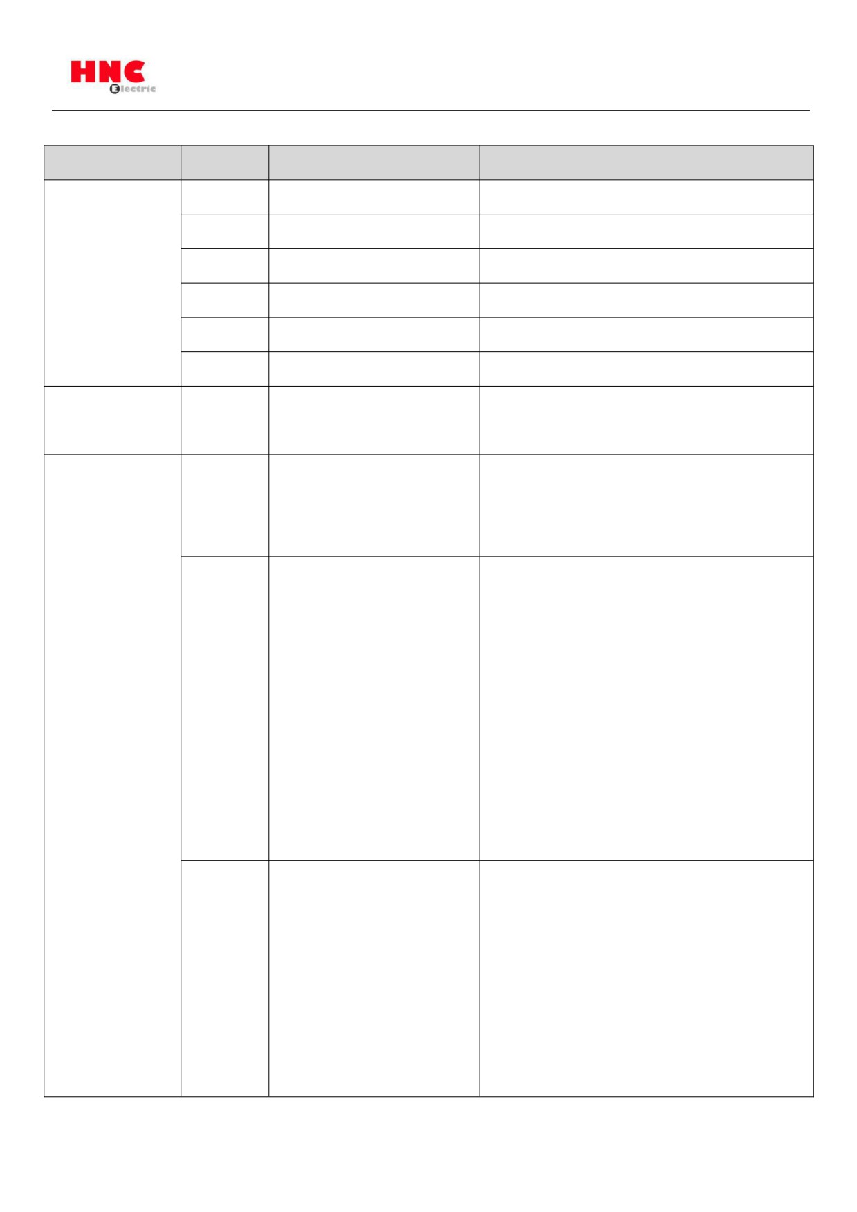
D4
red
Power Indicator
ON: The inverter is powered on;
OFF: The inverter is not connected to power or
the DP card is not installed properly.
D3
yellow
DP card and master station
ON: The DP card communicates with the
communication indicator
Profibus master station normally;
OFF: The DP card and the Profibus master
station failed to communicate (you can check
the slave address, data format, and connection
with the Profibus cable);
Indicator
Blinking: Indicates that there is interference
between the DP card and the Profibus master
station, intermittent.
D2
green
DP card and inverter
ON: The communication between the DP card
communication indicator
and the inverter is normal;
OFF: Communication between the DP card and
the inverter is unsuccessful (check whether the
baud rate setting is correct);
Blinking: There is interference between the DP
card and the inverter.
(86)
3. DP card and HV610 inverter communication configuration instructions
After the HV610-DP card is correctly installed on the HV610 inverter, the relevant communication
configuration needs to be completed before the DP card can establish communication with the
inverter.
Inverter communication card type setting
The function code Fd-00 needs to be set to 1, and Profibus-DP is selected as the serial
communication protocol of the inverter, as shown in the following table.
Parameter
Name
Set range
Set value
Description
Fd-00
Serial communication
0: Modbus
1
Serial communication with
protocol selection
1: Profibus-DP
DP card using
Profibus-DP protocol
4. DP card and Profibus master communication configuration instructions
After the DP card communicates with the HV610 inverter, it needs to be correctly wired with the
Profibus master station. Setting the relevant communication configuration can realize the
communication between the DP card and the Profibus master station, thereby achieving the
inverter networking function.
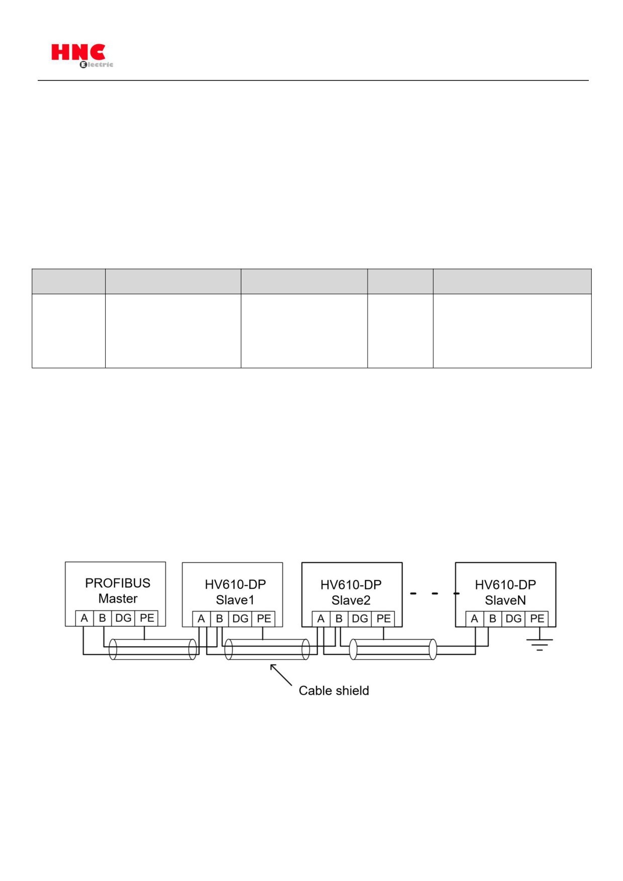
Wiring of DP card and Profibus master
The connection diagram between the DP card and the Profibus master station is shown below:
Figure 3 Schematic diagram of the connection between the DP card and the Profibus master station
In the Profibus bus terminal, it is necessary to access the terminal matching resistor, and the dialing
code can be dialed according to the indication on the terminal. The PE level of the system must be
reliably grounded.
(86)
According to the setting of the communication baud rate of the master station, the length of the
communication cable between the DP card and the Profibus master station is also required. The
length of the communication data cable must be restricted in strict accordance with the SIEMENS
DB9 wiring standard.
The baud rate and wire length requirements are shown in the following table:
Baud rate (Kbps)
Data wire A maximum length (m)
Data wire B maximum length (m)
9.6
1200
1200
19.2
1200
1200
187.5
600
600
500
200
200
1500
100
100
6000
100
100
12000
100
100
HV610 Profibus-DP slave address configuration
To realize the function of Profibus master-slave control inverter, HV610 Profibus-DP communication
slave address must be set. The slave address can be set by the DIP switch on the DP card, or by
the inverter function code Fd-03. The slave address of the HV610-DP card is set by the 3 to 8 bits
of the DIP switch, as shown in the following table:
DIP switch
Slave address
Profibus-DP
Bit 3 ~ Bit 8 six-digit binary DIP switch can set station address 0~63.
communication
Example:
Bit 3 ~ Bit 8
Local Address
slave address
00 0000
Fd-02 decision
00 0111
07
01 0100
20
(Note: When the DIP switch is set to 0, the local address is set by the HV610
inverter function code Fd-03)
When the HV610-DP DIP switch selection address is set to 0, the communication slave address is
set by the inverter function code Fd-03, as shown in the following table.
Parameter
Name
Set range
Default value
Description
Fd-03
Local address
0: broadcast address
1
DP support slave
1 ~ 249
station number is
1~125
(86)
Communication timeout detection setting
In order to determine whether the communication between the HV610-DP communication card and
the master station is interrupted, it is necessary to set the function code communication timeout
period (Fd-05). If the interval between one communication and the next communication exceeds
the communication timeout time, the inverter will report a communication failure error (COF).
Parameter
Name
Set range
Default value
Fd-05
Communication timeout
1
0.0s:Invalid
0.1s~60.0s
PPO data format selection
The PPO type is used as the data transmission format in the PROFIDRIVE (variable speed drive)
protocol. For details, see the description of the data format definition in the subsequent
communication protocol section. HV610 Profibus-DP protocol supports 4 data formats, PPO1,
PPO2, PPO3, PPO5 are set by the ten digits of the function code Fd-06, as shown in below table:
Parameter
Name
Set range
Default value
Fd-06
Modbus, Profibus-DP
Single digit: Modbus
30
communication data format
Tens digit: Profibus-DP
0: PPO1 format
1: PPO2 format
2: PPO3 format
3: PPO5 format
After the above information is configured, the inverter needs to be powered on again to take effect.
5. Profibus-DP communication protocol description
Data transfer format
In the PROFIDRIVE protocol, the PPO type is used as the data transmission format. There are five
types of PPO types: PPO1, PPO2, PPO3, PPO4, and PPO5. The HV610-DP card supports four
types of data formats: PPO1, PPO2, PPO3, and PPO5.
The functions that each data format can complete are as follows:
(86)
Data type
Function
Data type
Function
PPO1
◆ Single function parameter operation
PPO3
◆ Inverter command, frequency control
◆ Inverter command, frequency control
◆ Inverter status, running frequency reading
◆ Inverter status, running frequency reading
PPO2
◆ Single function parameter operation
PPO5
◆ Single function parameter operation
◆ Inverter command, frequency control
◆ Inverter command, frequency control
◆ Inverter status, running frequency reading
◆ Inverter status, running frequency reading
◆ 4 function parameters are written periodically
◆ 10 function parameters are written periodically
◆ 4 function parameters are be read periodically
◆ 10 function parameters are be read periodically
The data block contained in the PPO type data format is divided into two areas, namely the PKW
area (parameter area) and the PZD area (process data area). The HV610-DP card supports four
types of PPO data formats as shown below:
Figure 4 PPO type data format description
PKW area data description
The data in the PKW area mainly implements the reading and writing of the single function code of
the inverter by the master station, and the communication address of the inverter function code is
directly given by the communication data. The functions implemented are as follows:a) Read the
function parameters of the inverterb) Change of inverter function parameters.
◆ Data format
The data in the PKW area contains three sets of array areas, namely PKE, IND, and PWE. The
PKE data byte length is 2 bytes, IND is 2 bytes, and PWE is 4 bytes. The data format is shown in
the following table:
(86)
Master station sends data PKW
Write : parameter value
Command
Function code address
Reserved
Read: None
PKE
PKE
IND
IND
PWE
PWE
PWE
PWE
Inverter response data PKW
Success: return value
Command
Function code address
Reserved
Failed: error message
PKE
PKE
IND
IND
PWE
PWE
PWE
PWE
◆ Data description
Master sends data PKW description
Inverter response data PKW description
PKE
High 4 digits: command code
PKE
High 4 digits: Response code
0: No request
0: No request
1: Read function code parameter data
1: Function code parameter operation
2: Change function code parameter
is correct
data
7: Unable to execute
14: Change function code parameter
Low 8 bits: function code parameter
data and store it in EEPROM
address high bits
(The above command code is decimal
data)
Low 4 bits: reserved
Low 8 bits: function code parameter
address high bits
IND
High 8 bits: Function code parameter
IND
High 8 bits: Function code parameter
address lower bits
address lower bits
Low 8 bits: reserved
Low 8 bits: reserved
PWE
High 16 bits: reserved
PWE
When the request is successful:
Low 16 bits: Not used when read
parameter value
request; indicates parameter value
When the request fails: Error code
when write request
(consistent with MODBUS):
(86)
1: Incorrect password
2: Read and write command error
3: CRC check error
4: Invalid address
5: invalid parameter
6: Parameter change is invalid
7: System lock
8: Parameter is being stored
◆ Application examples
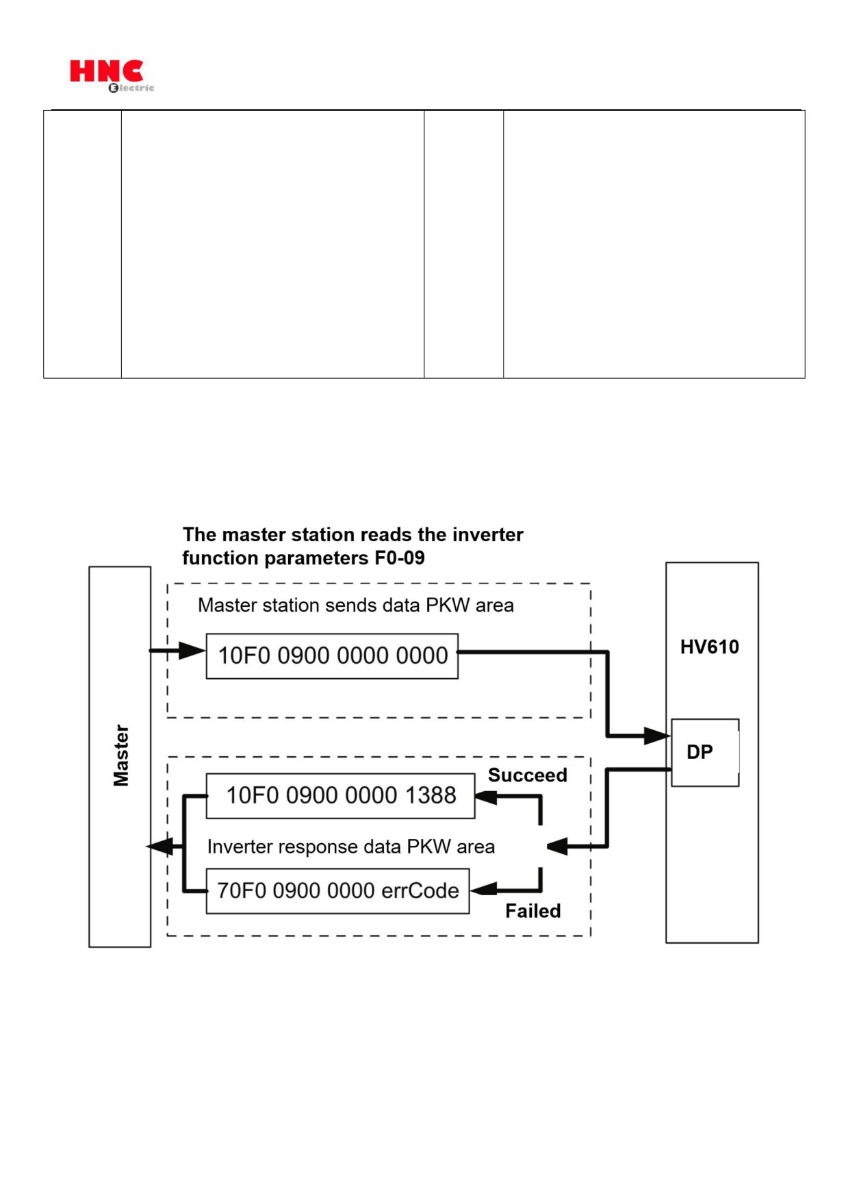
The master station reads the send data PKW area of the inverter function parameter F0-09 and the
drive response data PKW area as shown below:
Figure 5 Example of master station reading inverter parameters and sending PKW data
(86)
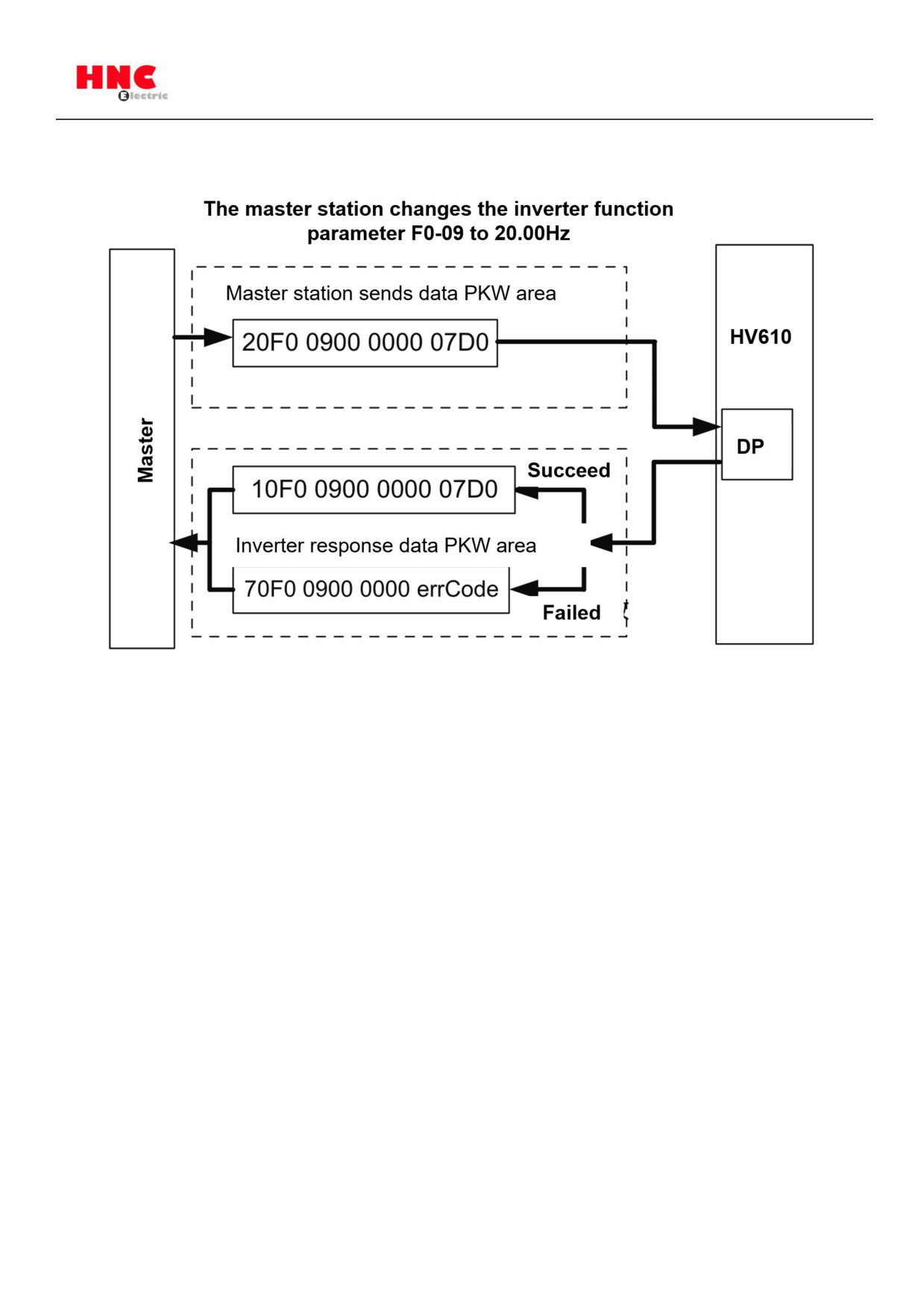
The master station changes the send data PKW area of the inverter function parameter F0-09 and
the inverter response data PKW area as shown below:
Figure 6 Example of master station writing inverter parameters and sending PKW data
The PKW data will interact with the inverter in a cyclic execution manner. If you use a write
command (PKE = 0x20xx) to continuously operate the EEPROM, the life of the inverter's main
control chip will be greatly reduced. If you need to change the parameters of the inverter's function
code, it is recommended to use PKW In the operation of the RAM address, the corresponding RAM
address of the function code F0 ~ FF group is 0x00 ~ 0x0F; the corresponding address of the A0 ~
AF group is 0x40 ~ 0x4F. For example, the corresponding RAM address of F0-10 is 0x000A.
PZD area data description
The data in the PZD area enables the master station to change and read the inverter data in real
time and perform periodic data interaction. The communication address of the data is directly
configured by the inverter. It mainly includes the following:a) Inverter control command and target
frequency given in real timeb) Real-time reading of inverter's current status and operating
frequencyc) Function parameter and monitoring parameter data real-time interaction between
inverter and PROFIBUS master stationThe PZD process data mainly completes the periodic data
exchange between the master station and the inverter. The interaction data is as follows:
(86)
Master station sends data PZD area
Commands
Inverter target frequency
Inverter function parameters change in real time
PZD1
PZD2
PZD3~PZD12
Inverter response data PZD area
Commands
Inverter running frequency
Inverter function parameters reading in real time
PZD1
PZD2
PZD3~PZD12
◆ Master sends data description
PZD1 and PZD2 are fixed configurations and cannot be modified by the user. PZD3 ~ PZD12 are
user-defined periodic data interactions, corresponding to the HV610 series inverter FE group
function code parameters. This group of parameters are user-defined parameters. The master
station sends data PZD3 ~ PZD12 corresponding to FE-00 ~ FE-09, and the inverter response data
PZD3 ~ PZD12 corresponds to FE-10 ~ FE-19. Modify the setting value of the FE group parameter
to exchange data with the master station. Setting the FE group parameter value to F0.00 means
skipping the data area.
◆ Application examples
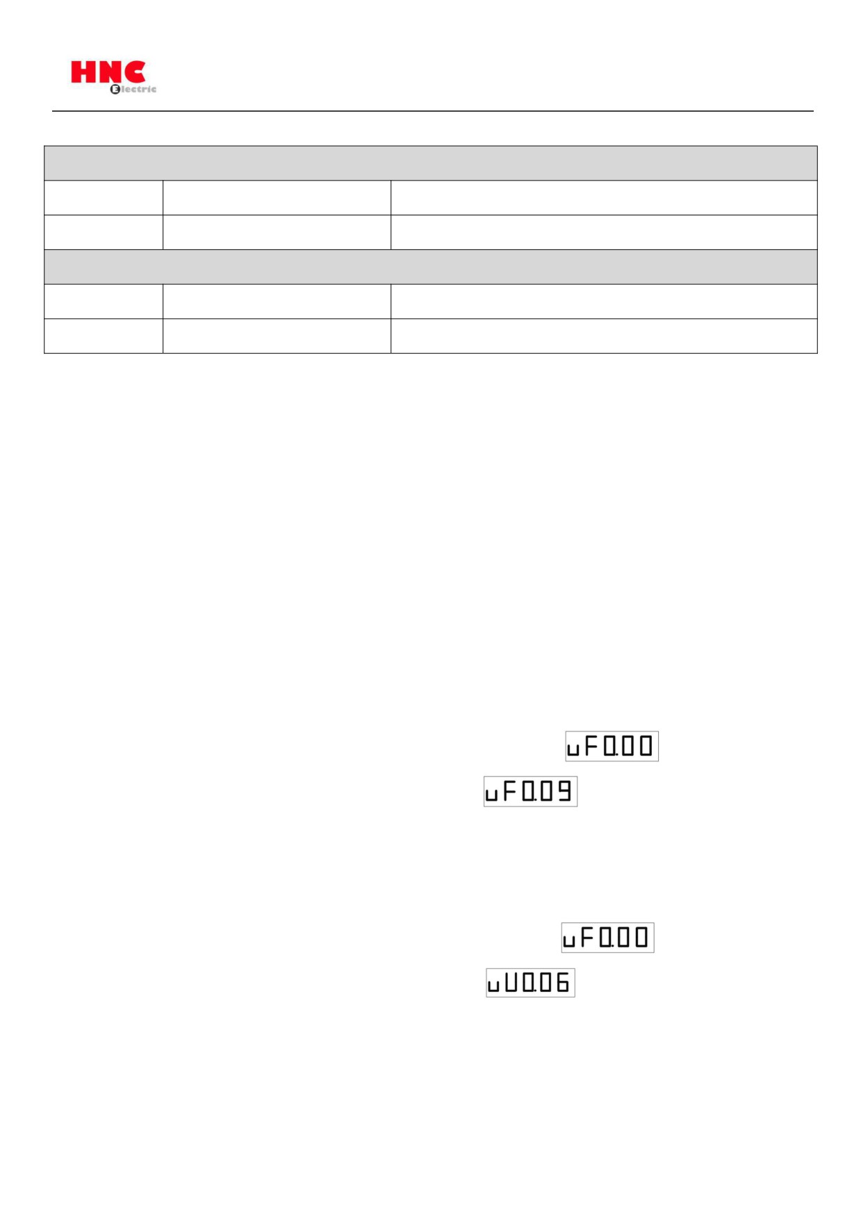
The master station periodically change the inverter's function parameter F0-09 through PZD3:
1. Enter FE-00, the initial keyboard display is shown in the figure:
2. Modified to F0-09, the keyboard display is as follows:
3. The master station periodically change the F0-09 function code by filling PZD3 data (do not write
EEPROM):
The master station periodically reads the inverter’s function parameter U0-06 through PZD3:
1. Enter FE-10. The initial keyboard display is shown in the figure.
2. Modified to U0-06, the keyboard display is as follows:
3. The master station reads the PZD3 data to realize U0-06: periodic reading output torque.
(86)
6. Configure GSD on the S7-300 master
When using the PROFIBUS master, you must first configure the .GSD file of the slave so that the
corresponding slave device is added to the system of the master .GSD files can be obtained from
HNC agents or manufacturers. The specific operations are as follows:
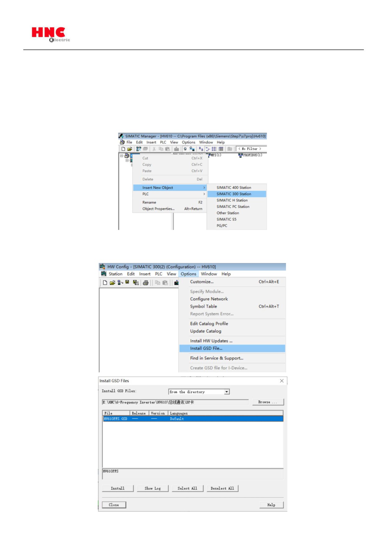
1. Build a project in STEP7, add the S7-300 master station to the project, as shown below:
2. Double-click the hardware logo to enter the HW config configuration, and add the
MD38PFS.GSD file in the HW config configuration screen, as follows:
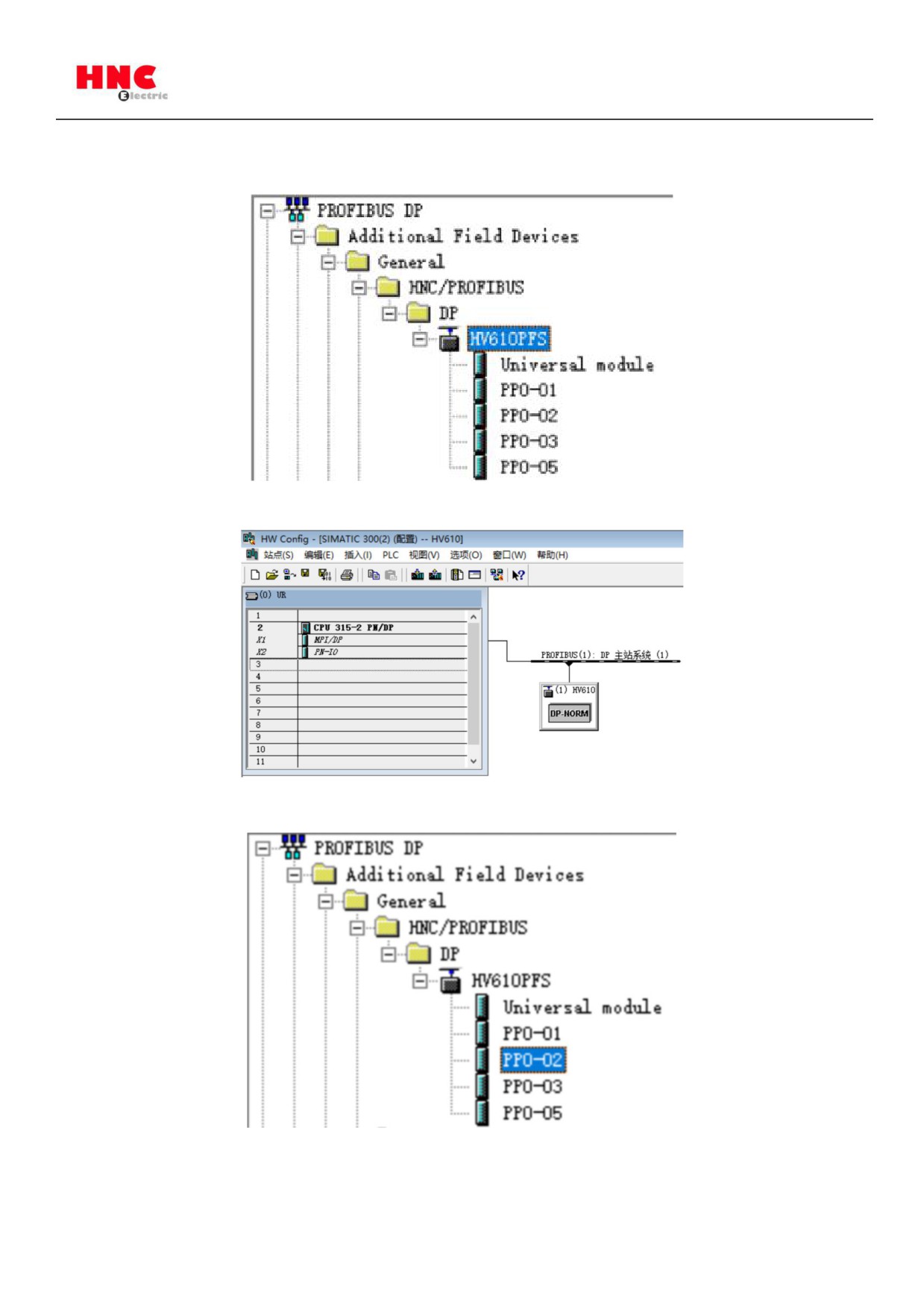
(86)
3. Click Install. After the installation is completed, there will be a PROFIBUS-DP module of
MD38PFS in the system.
4. The actual hardware system of the configuration system is shown below:
5. Configure the data characteristics of the slave:
All the above operations complete the operation of the PROFIBUS slave. You can control the
inverter by writing the corresponding program in S7-300.

(86)
7. Fault description and processing
Indicator
Fault state
Fault description
Troubleshoot
D4
Red
OFF
DP card is not powered on
Please check whether the DP card
and inverter interface are connected
well
D2
Green
Flicker
Intermittent connection
Please check whether the grounding
between DP card and inverter
is good and eliminate the interference
on site
D2
Green
OFF
The connection between the
Please check whether the setting of
DP card and the inverter is not
Profibus-DP baud rate function code
successful
(ten digits of Fd-01) is consistent with
the baud rate of the DIP switch.
D3
Yellow
Flicker
Intermittent connection
Please check whether the grounding
between DP card and Profibus
is good and eliminate the interference
master
on site
D2
Yellow
OFF
DP card and Profibus master
Please check if the slave address and
connection failed
data format are correct, if the Profibus
cable connection is normal, if the
slave address and data format are
configured correctly